KR950002274B1 - Mos vlsi device having shallow junctions and method of making the same - Google Patents
Mos vlsi device having shallow junctions and method of making the same Download PDFInfo
- Publication number
- KR950002274B1 KR950002274B1 KR1019860009058A KR860009058A KR950002274B1 KR 950002274 B1 KR950002274 B1 KR 950002274B1 KR 1019860009058 A KR1019860009058 A KR 1019860009058A KR 860009058 A KR860009058 A KR 860009058A KR 950002274 B1 KR950002274 B1 KR 950002274B1
- Authority
- KR
- South Korea
- Prior art keywords
- layer
- gate
- source
- drain regions
- silicon
- Prior art date
- Legal status (The legal status is an assumption and is not a legal conclusion. Google has not performed a legal analysis and makes no representation as to the accuracy of the status listed.)
- Expired - Lifetime
Links
Images



Classifications
-
- H—ELECTRICITY
- H10—SEMICONDUCTOR DEVICES; ELECTRIC SOLID-STATE DEVICES NOT OTHERWISE PROVIDED FOR
- H10D—INORGANIC ELECTRIC SEMICONDUCTOR DEVICES
- H10D62/00—Semiconductor bodies, or regions thereof, of devices having potential barriers
- H10D62/10—Shapes, relative sizes or dispositions of the regions of the semiconductor bodies; Shapes of the semiconductor bodies
- H10D62/13—Semiconductor regions connected to electrodes carrying current to be rectified, amplified or switched, e.g. source or drain regions
- H10D62/149—Source or drain regions of field-effect devices
- H10D62/151—Source or drain regions of field-effect devices of IGFETs
-
- H—ELECTRICITY
- H10—SEMICONDUCTOR DEVICES; ELECTRIC SOLID-STATE DEVICES NOT OTHERWISE PROVIDED FOR
- H10D—INORGANIC ELECTRIC SEMICONDUCTOR DEVICES
- H10D30/00—Field-effect transistors [FET]
- H10D30/01—Manufacture or treatment
- H10D30/021—Manufacture or treatment of FETs having insulated gates [IGFET]
- H10D30/027—Manufacture or treatment of FETs having insulated gates [IGFET] of lateral single-gate IGFETs
- H10D30/0275—Manufacture or treatment of FETs having insulated gates [IGFET] of lateral single-gate IGFETs forming single crystalline semiconductor source or drain regions resulting in recessed gates, e.g. forming raised source or drain regions
-
- H—ELECTRICITY
- H10—SEMICONDUCTOR DEVICES; ELECTRIC SOLID-STATE DEVICES NOT OTHERWISE PROVIDED FOR
- H10D—INORGANIC ELECTRIC SEMICONDUCTOR DEVICES
- H10D64/00—Electrodes of devices having potential barriers
- H10D64/01—Manufacture or treatment
- H10D64/011—Manufacture or treatment of electrodes ohmically coupled to a semiconductor
- H10D64/0111—Manufacture or treatment of electrodes ohmically coupled to a semiconductor to Group IV semiconductors
- H10D64/0112—Manufacture or treatment of electrodes ohmically coupled to a semiconductor to Group IV semiconductors using conductive layers comprising silicides
-
- H—ELECTRICITY
- H10—SEMICONDUCTOR DEVICES; ELECTRIC SOLID-STATE DEVICES NOT OTHERWISE PROVIDED FOR
- H10D—INORGANIC ELECTRIC SEMICONDUCTOR DEVICES
- H10D64/00—Electrodes of devices having potential barriers
- H10D64/20—Electrodes characterised by their shapes, relative sizes or dispositions
- H10D64/23—Electrodes carrying the current to be rectified, amplified, oscillated or switched, e.g. sources, drains, anodes or cathodes
- H10D64/251—Source or drain electrodes for field-effect devices
- H10D64/258—Source or drain electrodes for field-effect devices characterised by the relative positions of the source or drain electrodes with respect to the gate electrode
Landscapes
- Insulated Gate Type Field-Effect Transistor (AREA)
- Thin Film Transistor (AREA)
- Electrodes Of Semiconductors (AREA)
Abstract
내용 없음.No content.
Description
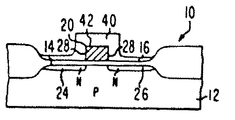
제 1 도 내지 5도는 본 발명의 기술에 대한 하나의 실시예를 보인 반도체 장치의 일부를 여러 단계의 완성으로 도시한 개략 단면도.1 through 5 are schematic cross-sectional views showing a part of a semiconductor device showing one embodiment of the technology of the present invention in several stages of completion;
제 6 도 내지 10도는 본 발명의 또 다른 실시예를 도시한 제1 내지 5도와 유사한 단면도.6 through 10 are cross-sectional views similar to the first through fifth views showing yet another embodiment of the present invention.
* 도면의 주요부분에 대한 부호의 설명* Explanation of symbols for main parts of the drawings
10, 100 : 반도체 장치 12 : 본체10, 100: semiconductor device 12: main body
20, 100 : 게이트 24 : 소오스 영역20, 100: gate 24: source region
26 : 드레인 영역 40 : 보호층26
50 : 에피택셜층 54 : 내화금속 규소화물층50: epitaxial layer 54: refractory metal silicide layer
112 : 실리콘 질화물층112: silicon nitride layer
본 발명은 MOS VLSI 장치의 매우 얕은(shallow) PN 접합부에 관한 것이다.The present invention relates to a very shallow PN junction of a MOS VLSI device.
집적회로 장치의 높은 패킹(packing) 밀도가 일반적으로 각각의 성분 크기를 줄이고 이와 대응하여 접합부 깊이 및 다른 디멘젼의 성분 요소를 줄이는 것에 의해 실현된다. FET 크기를 비율에 따라 줄일 경우, 접합부 깊이는 잘 알려진 펀치-관통 현상의 바람직하지 못한 발생을 방지하기 위해 매우 얕게 형성되어야 한다. 여러 성분 요소들의 차원에 대한 이러한 감소 때문에 이 요소들의 시이트 저항이 증가된다. 이러한 것은 MOS 피일드 이펙트 트랜지스터(MOSFET)의 소오스 및 드레인 영역과 같은 비교적 협소하고 얕게 도우핑된 영역들에 대해, 이 영역들을 상호접속으로 사용하는데 어려움이 있고 소오스 및 드레인의 높은 시리즈 저항이 구동전류를 감소시키며 이에 의해 장치 수행의 능력을 떨어뜨린다는 점에서 심각한 문제를 발생시킨다.High packing densities of integrated circuit devices are generally realized by reducing each component size and correspondingly reducing the component depth of the junction depth and other dimensions. When the FET size is reduced proportionally, the junction depth should be made very shallow to prevent the undesirable occurrence of the well-known punch-through phenomenon. This reduction in the dimensions of the various component elements increases the sheet resistance of these elements. This makes it difficult to use these regions as interconnects for relatively narrow and shallowly doped regions, such as source and drain regions of MOS feed effect transistors (MOSFETs) and the high series resistance of the source and drain leads to drive current. A serious problem arises in that it reduces the performance of the device and thereby decreases the performance of the device.
이 문제에 대한 하나의 해결책은 상기 전기 저항을 감소시키기 위해 소오스 및 드레인 영역 표면을 규소화하는 것이다. 이러한 해결책이 1983년 5월17일자 Tasch, jr. 등에 허여된 미합중국 특허 제4,384,301호에 기재되어 있다. 여기에는 소오스와 드레인의 접촉표면이 금속 규소화물을 구비하는 MOSFET가 기재되어 있다. 그러나, 이러한 구조에 전혀 문제점이 없는 것은 아니다.One solution to this problem is to siliconize the source and drain region surfaces to reduce the electrical resistance. This solution is described in Tasch, jr. US Patent No. 4,384,301 to et al. Here, a MOSFET is described in which the contact surface between the source and the drain includes a metal silicide. However, this structure is not without any problem.
어느 내화금속 또는 이 금속의 규소화물과 도우핑된 실리콘 사이의 접촉저항은 실리콘 경계면에 대한 규소화물의 도우핑 농도에 강하게 의존한다. 통상, 작은 저항을 갖는 접촉을 얻기 위해, 경계면에서의 실리콘은 약 1020원자/㎤의 도우핑 농도를 가져야 한다. 이러한 높은 도우핑 레벨을 갖는 매우 얕은 소오스 및 드레인 영역을 제조하는 것은 실질상 불가능하다.The contact resistance between any refractory metal or its silicide and doped silicon is strongly dependent on the doping concentration of the silicide on the silicon interface. Typically, to obtain a contact with a small resistance, the silicon at the interface should have a doping concentration of about 10 20 atoms / cm 3. It is practically impossible to produce very shallow source and drain regions with such high doping levels.
본 발명에 따라서, MOSFET 장치 및 그 제조방법이 기재 되었다. 이 FET는 표면과, 이 표면상에 형성된 절연 게이트와, 이 게이트의 측벽에 인접하여 형성되고 상기 표면으로부터 100nm 보다 작은 깊이까지 아래로 연장하는 소오스와 드레인 영역을 포함한다. 상기 방법은 (a) 절연 게이트를 형성하고, (b) 이 게이트의 측벽에 인접하여 소오스 및 드레인 영역을 형성하여 이 영역들이 상기 표면으로부터 100nm 보다 작은 깊이까지 연장하게 하고, (c) 전체 게이트를 걸쳐서 보호층을 형성하며, (d) 소오스 및 드레인 영역의 표면에 단결정 실리콘층을 형성하고, (e) 이 실리콘층을 그층 두께와 대략 같은 깊이로 도우핑하며, (f) 실리콘층에 금속 규소화 물층을 형성하는 단계들을 포함한다. 이하 도면을 참조로하여 본 발명을 상세히 설명하기로 한다.According to the present invention, a MOSFET device and a method of manufacturing the same have been described. The FET includes a surface, an insulating gate formed on the surface, and source and drain regions formed adjacent to the sidewalls of the gate and extending down to a depth less than 100 nm from the surface. The method comprises (a) forming an insulated gate, (b) forming source and drain regions adjacent the sidewalls of the gate such that these regions extend to a depth less than 100 nm from the surface, and (c) (D) forming a single crystal silicon layer on the surface of the source and drain regions, (e) doping the silicon layer to a depth approximately equal to its thickness, and (f) forming a metal layer on the silicon layer. Forming a layer of extinguishing water. Hereinafter, the present invention will be described in detail with reference to the accompanying drawings.
이하 기재 및 제 1 도 내지 제10도에 도시된 바와 같이, 특정한 p 및 N 전도형 물질과 영역들이 보여진다. 이것은 본 발명의 실시예에 의해서 보여지며 본 발명의 기술의 범위를 제한한다고 생각되지 않을 것이다. 서로 마주보는 p 및 N 정렬을 갖는 장치가 본 명세서에 기재된 장치에 관하여 모든 것에서 동일하게 고려된 것이 이해 될 것이다.Specific p and N conducting materials and regions are shown, as shown below in the substrate and FIGS. 1-10. This is shown by the embodiments of the present invention and will not be considered to limit the scope of the present technology. It will be understood that devices with p and N alignments facing each other are considered equally in all respects with respect to the devices described herein.
플라나 표면(14)을 갖는 제 1 전도형 물질의 본체(12)를 포함하는 반도체 장치(10)의 일부분이 제 1 도에서 제 5 도를 통하여 도시되어 있고, 상기 물질은 본 발명의 실시예에서 저도우핑된 p형인 실리콘과 같은 것이다. 실리콘 산화물과 같은 절연체의 비교적 얇은 층(16)이 제 1 도에 도시된 바와 같이 플라나 표면(14)에 증착된다.A portion of a
다결정 실리콘으로 되어 있고 본 발명의 실시예에서 고도우핑 된 N형이며 약 1㎛의 길이를 갖는 절연게이트(20)가 기술상 잘 알려진 방법으로 층(16)에 형성된다.
상기 장치(10)는 이어서 제 1 도의 부호(22)에 도시된 바와 같이 약 1012이온/㎤의 농도에서 대략 10kev인 비교적 낮은 에너지의 비소 이식을 받는다. 이 낮은 에너지 이식은 매우 얕은 소오스 및 드레인 영역(24, 26)이 게이트(20)의 측벽(28)에 인접하여 형성되는 것을 초래할 것이다. 상기 영역들(24, 26)이 표면(14)으로부터 본체(12)안으로 연장하는 깊이는 약 100nm 보다 작게 되어야 한다. 산화물의 보호층(40)이 이어서 약 800-900℃ 온도의 증기 주위 분위기에서 성장된다. 이 산화 처리가 고도우핑된 실리콘 표면에는 산화물의 비교적 두꺼운 층을, 저도우핑된 실리콘 표면에는 산화물의 상기 두꺼운 층보다 얇은 층을 성장시킬 것이기 때문에, 산화물의 보호층(40)은 상기 얇은 층(16)보다는 실질상 두껍다. 상기 층(40)이 약 200-500nm의 두께로 성장해야 하는 반면에, 소오스 및 드레인 영역(24, 26)을 걸쳐서 표면에 증착된 산화물층(16)이 제 2 도에 도시된 바와 같이 약 40-100nm 보다 두껍지는 않을 것이다(제 2 도 참조). 상기 장치(10)는 이어서 플라즈마 비등방성 에칭을 받으며, 층(16)의 모든 산화물이 소오스 및 드레인 영역(24, 26)을 걸쳐서 직접 표면으로부터 제거될 때까지 계속된다. 게이트(20) 상부의 두께가 제 3 도에 도시된 바와 같이 다소 감소될 지라도, 이 게이트 (20)의 측벽(28) 및 상부(42)의 산화물이 본래대로 남게될 것이고 이에 의해 게이트를 완전히 덮을 것이다.The
단결정 실리콘의 에피택셜층(50)이 통상의 방법으로 소오스 및 드레인 영역(24, 26)을 걸쳐서 직접 실리콘의 표면으로부터 선택적으로 성장된다(제 4 도 참조). 상기 층(50)은 게이트 전극(20)의 두께 보다 크지 않은 두께로 성장되어야 한다. 이 층(50)은 이어서 제 4 도의 부호(52)로 도시된 비교적 높은 에너지의 비소이식을 받게 되어 그 층 두께와 대략 같거나 약간 작은 깊이까지 아래로 상기 층(50)을 고도우핑하게 한다. 소오스 및 드레인 영역(24, 26)의 불순물중 약간이 에피택셜층(50)안으로 위쪽을 향하여 짧은 거리로 확산할 것이다. 그러므로, 이온 이식제가 이러한 위쪽으로 확산된 영역안의 웰(well) 깊이에 오직 도착할 필요가 있다. 상기 이온 이식이 소오스 및 드레인 영역(24, 26)의 깊이 보다 더 깊게 연장하지 않도록 주의해야 한다. 내화금속 규소화물층(54)이 이어서 티타늄 또는 텅스텐과 같은 내화금속층을 증착시키는 것에 의해, 고도우핑된 에피택셜층에 형성되고, 이어서 상기 장치(10)를 충분히 가열하여 내화금속이 표면(14)에서 실리콘과 배합하여 이에 의해 금속 규소화물을 형성할 때까지 계속 가열한다. 이 층(54)은 매우 얕은 소오스 및 드레인 영역(24, 26)에 대해 소정의 저 저항 접촉을 형성한다.The
본 발명의 또 다른 실시예가 제 6 도에서 제10도를 통하여 도시되어 있다. 여기에는, 장치(10)의 특징에 유사한 구조적 특징을 갖고 유사하게 동일한 번호가 도시된 반도체 장치(100)의 일부분이 도시되어 있다. 이러한 유사한 특징은 다시는 기재되지 않을 것이다. 이 두 장치들(10, 100)사이의 중요한 차이점은 장치(100)가 적당한 금속 또는 금속 규소화물로 구성된 게이트(110)를 갖고 있다는 점이다. 산화물의 보호층(40)이 금속 게이트상에 성장될 수 없고 금소 규소화물 게이트가 저도우핑된 실리콘과 유사한 속도로 산화할 수 있기 때문에, 다른 수단이 에피택셜층(50)의 성장기간 동안 게이트 전극을 절연시키는데 사용되어야 한다. 이러한 목적을 위해서, 실리콘 질화물층(112)이 어느 적당한 방법으로 게이트(110)의 상부 표면(42)에 형성된다. 약 200nm에서 약 500nm까지의 두께를 갖는 적합한 산화물층(114)이 이어서 통상의 방법, 예를 들어 CVD 처리에 의해 상기 장치(100)에 형성된다(제 7 도 참조).Another embodiment of the present invention is shown in FIGS. 6 through 10. Here, a portion of the
상기 장치(100)는 이어서 층(16, 114)의 모든 산화물이 제 8 도에 도시된 바와 같이 소오스 및 드레인 영역(24, 26)을 걸쳐서 직접 표면(14)으로부터 제저될 때까지 프라즈마 비등방성 에칭을 받는다. 제 8 도, 9도 및 10도에 도시된 바와 같이, 산화물층(116)이 게이트(110)의 측벽(28)에 남게될 것이고, 실리콘 질화물층(112) 상부로 짧은 거리내에서 위쪽으로 연장할 것이다. 장치(10)에서와 같이, 에피택셜층(50)이 장치(100)의 소오스 및 드레인 영역(24, 26)에서 성장되고, 상기 층(50)이 이어서 이온 이식제(52)를 받으며, 이어서 내화금속 규소화물층(54)이 제 9 도 및 10도에 도시된 바와 같이 상기 영역에 형성된다. 실리콘 질화물층(112)은 통상의 방법으로 임의로 제거될 수도 있다.The
본 발명의 중요한 잇점은 단지 100nm 또는 그 보다 작은 깊이를 갖는 얕은 소오스 및 드레인 영역에 대해 매우 낮은 시이트 저항을 얻는 다는 점이다. 또한, 이 처리방법은 MOSFET의 채널 영역안으로 불순물의 측방향 확산을 유도하지 않고, 이에 의해 최종 채널 깊이의 제조상 제어를 보장하는 것을 돕니다. 게이트 측벽상의 산화물의 보호층이 비교적 두껍게 형성될 수도 있으며, 이 게이트 측벽의 커패시턴스가 종래의 MOSFET 보다 크지 않도록 제어될 수 있다. 또 다른 잇점은 설명된 처리 방법에서 가지고 있는 게이트 전극의 부분적 매몰에 의해 상기 장치의 표면 형태가 상당히 편평하다는 점이다.An important advantage of the present invention is that very low sheet resistance is obtained for shallow source and drain regions having only a depth of 100 nm or less. In addition, this method does not induce lateral diffusion of impurities into the MOSFET's channel region, thereby helping to ensure manufacturing control of the final channel depth. A protective layer of oxide on the gate sidewall may be formed relatively thick and can be controlled so that the capacitance of the gate sidewall is not greater than a conventional MOSFET. Another advantage is that the surface morphology of the device is quite flat due to the partial embedding of the gate electrode with the described processing method.
Claims (19)
Applications Claiming Priority (2)
| Application Number | Priority Date | Filing Date | Title |
|---|---|---|---|
| US792,789 | 1985-10-30 | ||
| US06/792,789 US4841347A (en) | 1985-10-30 | 1985-10-30 | MOS VLSI device having shallow junctions and method of making same |
Publications (2)
| Publication Number | Publication Date |
|---|---|
| KR870004518A KR870004518A (en) | 1987-05-11 |
| KR950002274B1 true KR950002274B1 (en) | 1995-03-15 |
Family
ID=25158076
Family Applications (1)
| Application Number | Title | Priority Date | Filing Date |
|---|---|---|---|
| KR1019860009058A Expired - Lifetime KR950002274B1 (en) | 1985-10-30 | 1986-10-29 | Mos vlsi device having shallow junctions and method of making the same |
Country Status (5)
| Country | Link |
|---|---|
| US (1) | US4841347A (en) |
| JP (1) | JPH07120796B2 (en) |
| KR (1) | KR950002274B1 (en) |
| DE (1) | DE3636249A1 (en) |
| SE (1) | SE8604541L (en) |
Families Citing this family (23)
| Publication number | Priority date | Publication date | Assignee | Title |
|---|---|---|---|---|
| JPS63283161A (en) * | 1987-05-15 | 1988-11-21 | Toshiba Corp | Semiconductor device and manufacture thereof |
| US4786609A (en) * | 1987-10-05 | 1988-11-22 | North American Philips Corporation, Signetics Division | Method of fabricating field-effect transistor utilizing improved gate sidewall spacers |
| CA1308496C (en) | 1988-02-18 | 1992-10-06 | Rajiv V. Joshi | Deposition of tungsten on silicon in a non-self-limiting cvd process |
| JP2870757B2 (en) * | 1988-05-31 | 1999-03-17 | ソニー株式会社 | Method for manufacturing MIS transistor |
| US4998150A (en) * | 1988-12-22 | 1991-03-05 | Texas Instruments Incorporated | Raised source/drain transistor |
| EP0410390A3 (en) * | 1989-07-27 | 1993-02-24 | Seiko Instruments Inc. | Method of producing semiconductor device |
| JPH0671073B2 (en) * | 1989-08-29 | 1994-09-07 | 株式会社東芝 | Semiconductor device and manufacturing method thereof |
| US5006911A (en) * | 1989-10-02 | 1991-04-09 | Motorola, Inc. | Transistor device with high density contacts |
| JP3431647B2 (en) | 1992-10-30 | 2003-07-28 | 株式会社半導体エネルギー研究所 | Semiconductor device, method for manufacturing same, method for manufacturing memory device, and method for laser doping |
| EP0709880A3 (en) * | 1994-10-31 | 1996-10-23 | Sgs Thomson Microelectronics | Method for forming projecting source / drain regions in an integrated circuit |
| US5683924A (en) * | 1994-10-31 | 1997-11-04 | Sgs-Thomson Microelectronics, Inc. | Method of forming raised source/drain regions in a integrated circuit |
| US5682055A (en) * | 1995-06-07 | 1997-10-28 | Sgs-Thomson Microelectronics, Inc. | Method of forming planarized structures in an integrated circuit |
| US6043129A (en) * | 1997-06-09 | 2000-03-28 | Integrated Device Technology, Inc. | High density MOSFET with raised source and drain regions |
| US6063676A (en) * | 1997-06-09 | 2000-05-16 | Integrated Device Technology, Inc. | Mosfet with raised source and drain regions |
| US6121120A (en) * | 1997-08-07 | 2000-09-19 | Nec Corporation | Method for manufacturing semiconductor device capable of flattening surface of selectively-grown silicon layer |
| US5998248A (en) * | 1999-01-25 | 1999-12-07 | International Business Machines Corporation | Fabrication of semiconductor device having shallow junctions with tapered spacer in isolation region |
| US6025242A (en) * | 1999-01-25 | 2000-02-15 | International Business Machines Corporation | Fabrication of semiconductor device having shallow junctions including an insulating spacer by thermal oxidation creating taper-shaped isolation |
| US5998273A (en) * | 1999-01-25 | 1999-12-07 | International Business Machines Corporation | Fabrication of semiconductor device having shallow junctions |
| US6022771A (en) * | 1999-01-25 | 2000-02-08 | International Business Machines Corporation | Fabrication of semiconductor device having shallow junctions and sidewall spacers creating taper-shaped isolation where the source and drain regions meet the gate regions |
| US6187617B1 (en) | 1999-07-29 | 2001-02-13 | International Business Machines Corporation | Semiconductor structure having heterogeneous silicide regions and method for forming same |
| US7831518B2 (en) * | 2001-11-20 | 2010-11-09 | Psi Systems, Inc. | Systems and methods for detecting postage fraud using an indexed lookup procedure |
| DE10212914A1 (en) * | 2002-03-22 | 2003-10-16 | Infineon Technologies Ag | Manufacturing method for a contact in a semiconductor structure and corresponding contact |
| US7414277B1 (en) * | 2005-04-22 | 2008-08-19 | Spansion, Llc | Memory cell having combination raised source and drain and method of fabricating same |
Family Cites Families (8)
| Publication number | Priority date | Publication date | Assignee | Title |
|---|---|---|---|---|
| JPS5664467A (en) * | 1979-10-31 | 1981-06-01 | Chiyou Lsi Gijutsu Kenkyu Kumiai | Mos type semiconductor device |
| US4384301A (en) * | 1979-11-07 | 1983-05-17 | Texas Instruments Incorporated | High performance submicron metal-oxide-semiconductor field effect transistor device structure |
| JPS584924A (en) * | 1981-07-01 | 1983-01-12 | Hitachi Ltd | Forming method for semiconductor device electrode |
| US4476475A (en) * | 1982-11-19 | 1984-10-09 | Northern Telecom Limited | Stacked MOS transistor |
| JPS59115562A (en) * | 1982-12-22 | 1984-07-04 | Toshiba Corp | Manufacture of mosfet |
| JPS6014461A (en) * | 1983-07-04 | 1985-01-25 | Hitachi Ltd | Complementary insulated gate field-effect transistor |
| JPS613461A (en) * | 1984-06-18 | 1986-01-09 | Nec Corp | Manufacturing method of semiconductor device |
| JPS6161463A (en) * | 1984-09-03 | 1986-03-29 | Oki Electric Ind Co Ltd | Semiconductor integrated circuit device and its manufacturing method |
-
1985
- 1985-10-30 US US06/792,789 patent/US4841347A/en not_active Expired - Fee Related
-
1986
- 1986-10-23 SE SE8604541A patent/SE8604541L/en not_active Application Discontinuation
- 1986-10-24 DE DE19863636249 patent/DE3636249A1/en not_active Withdrawn
- 1986-10-28 JP JP61258053A patent/JPH07120796B2/en not_active Expired - Fee Related
- 1986-10-29 KR KR1019860009058A patent/KR950002274B1/en not_active Expired - Lifetime
Also Published As
| Publication number | Publication date |
|---|---|
| JPH07120796B2 (en) | 1995-12-20 |
| DE3636249A1 (en) | 1987-05-07 |
| JPS63115376A (en) | 1988-05-19 |
| KR870004518A (en) | 1987-05-11 |
| SE8604541L (en) | 1987-05-01 |
| US4841347A (en) | 1989-06-20 |
| SE8604541D0 (en) | 1986-10-23 |
Similar Documents
| Publication | Publication Date | Title |
|---|---|---|
| KR950002274B1 (en) | Mos vlsi device having shallow junctions and method of making the same | |
| US4038107A (en) | Method for making transistor structures | |
| EP0094891B1 (en) | Method of fabricating a vertical power mosfet structure | |
| US6614075B2 (en) | Semiconductor device and method of manufacturing the same | |
| US4931408A (en) | Method of fabricating a short-channel low voltage DMOS transistor | |
| US6043126A (en) | Process for manufacture of MOS gated device with self aligned cells | |
| KR100440840B1 (en) | Method of manufacturing semiconductor device and semiconductor device | |
| JP3704164B2 (en) | Method for forming shallow semiconductor junction | |
| US5382536A (en) | Method of fabricating lateral DMOS structure | |
| JP2002520851A (en) | Method for manufacturing power semiconductor device | |
| JPH0846200A (en) | Integrated structure MOS technology high-speed power device and manufacturing method thereof | |
| US5932913A (en) | MOS transistor with controlled shallow source/drain junction, source/drain strap portions, and source/drain electrodes on field insulation layers | |
| KR970011641B1 (en) | Semiconductor device and method of manufacturing the same | |
| US4826782A (en) | Method of fabricating aLDD field-effect transistor | |
| US4994881A (en) | Bipolar transistor | |
| US7208383B1 (en) | Method of manufacturing a semiconductor component | |
| KR950008257B1 (en) | MOS transistor and its manufacturing method | |
| KR100300892B1 (en) | Method of manufacturing a semiconductor device whereby a laterally bounded semiconductor zone is formed in a semiconductor body in a self-aligning manner | |
| KR100257074B1 (en) | Mosfet and method for manufacturing the same | |
| JPH11330439A (en) | Method of forming ultra-thin SOI electrostatic discharge protection element | |
| JP2002057118A (en) | Semiconductor device and manufacturing method thereof | |
| JPS6225457A (en) | Manufacturing method of vertical semiconductor device | |
| JPS6246570A (en) | Vertical type semiconductor device and manufacture thereof | |
| JPH0541516A (en) | Semiconductor device and its manufacture | |
| JPH04255233A (en) | Semiconductor device and manufacture thereof |
Legal Events
| Date | Code | Title | Description |
|---|---|---|---|
| PA0109 | Patent application |
St.27 status event code: A-0-1-A10-A12-nap-PA0109 |
|
| R17-X000 | Change to representative recorded |
St.27 status event code: A-3-3-R10-R17-oth-X000 |
|
| PG1501 | Laying open of application |
St.27 status event code: A-1-1-Q10-Q12-nap-PG1501 |
|
| A201 | Request for examination | ||
| PA0201 | Request for examination |
St.27 status event code: A-1-2-D10-D11-exm-PA0201 |
|
| G160 | Decision to publish patent application | ||
| PG1605 | Publication of application before grant of patent |
St.27 status event code: A-2-2-Q10-Q13-nap-PG1605 |
|
| E701 | Decision to grant or registration of patent right | ||
| PE0701 | Decision of registration |
St.27 status event code: A-1-2-D10-D22-exm-PE0701 |
|
| NORF | Unpaid initial registration fee | ||
| PC1904 | Unpaid initial registration fee |
St.27 status event code: A-2-2-U10-U13-oth-PC1904 St.27 status event code: N-2-6-B10-B12-nap-PC1904 |
|
| P22-X000 | Classification modified |
St.27 status event code: A-2-2-P10-P22-nap-X000 |
|
| P22-X000 | Classification modified |
St.27 status event code: A-2-2-P10-P22-nap-X000 |
|
| P22-X000 | Classification modified |
St.27 status event code: A-2-2-P10-P22-nap-X000 |