KR20240002442A - Light emitting display device and repair method of the same - Google Patents
Light emitting display device and repair method of the same Download PDFInfo
- Publication number
- KR20240002442A KR20240002442A KR1020220079653A KR20220079653A KR20240002442A KR 20240002442 A KR20240002442 A KR 20240002442A KR 1020220079653 A KR1020220079653 A KR 1020220079653A KR 20220079653 A KR20220079653 A KR 20220079653A KR 20240002442 A KR20240002442 A KR 20240002442A
- Authority
- KR
- South Korea
- Prior art keywords
- line
- metal layer
- branch
- light emitting
- display device
- Prior art date
- Legal status (The legal status is an assumption and is not a legal conclusion. Google has not performed a legal analysis and makes no representation as to the accuracy of the status listed.)
- Pending
Links
Images


Classifications
-
- G—PHYSICS
- G09—EDUCATION; CRYPTOGRAPHY; DISPLAY; ADVERTISING; SEALS
- G09G—ARRANGEMENTS OR CIRCUITS FOR CONTROL OF INDICATING DEVICES USING STATIC MEANS TO PRESENT VARIABLE INFORMATION
- G09G3/00—Control arrangements or circuits, of interest only in connection with visual indicators other than cathode-ray tubes
- G09G3/20—Control arrangements or circuits, of interest only in connection with visual indicators other than cathode-ray tubes for presentation of an assembly of a number of characters, e.g. a page, by composing the assembly by combination of individual elements arranged in a matrix no fixed position being assigned to or needed to be assigned to the individual characters or partial characters
- G09G3/22—Control arrangements or circuits, of interest only in connection with visual indicators other than cathode-ray tubes for presentation of an assembly of a number of characters, e.g. a page, by composing the assembly by combination of individual elements arranged in a matrix no fixed position being assigned to or needed to be assigned to the individual characters or partial characters using controlled light sources
- G09G3/30—Control arrangements or circuits, of interest only in connection with visual indicators other than cathode-ray tubes for presentation of an assembly of a number of characters, e.g. a page, by composing the assembly by combination of individual elements arranged in a matrix no fixed position being assigned to or needed to be assigned to the individual characters or partial characters using controlled light sources using electroluminescent panels
- G09G3/32—Control arrangements or circuits, of interest only in connection with visual indicators other than cathode-ray tubes for presentation of an assembly of a number of characters, e.g. a page, by composing the assembly by combination of individual elements arranged in a matrix no fixed position being assigned to or needed to be assigned to the individual characters or partial characters using controlled light sources using electroluminescent panels semiconductive, e.g. using light-emitting diodes [LED]
- G09G3/3208—Control arrangements or circuits, of interest only in connection with visual indicators other than cathode-ray tubes for presentation of an assembly of a number of characters, e.g. a page, by composing the assembly by combination of individual elements arranged in a matrix no fixed position being assigned to or needed to be assigned to the individual characters or partial characters using controlled light sources using electroluminescent panels semiconductive, e.g. using light-emitting diodes [LED] organic, e.g. using organic light-emitting diodes [OLED]
- G09G3/3225—Control arrangements or circuits, of interest only in connection with visual indicators other than cathode-ray tubes for presentation of an assembly of a number of characters, e.g. a page, by composing the assembly by combination of individual elements arranged in a matrix no fixed position being assigned to or needed to be assigned to the individual characters or partial characters using controlled light sources using electroluminescent panels semiconductive, e.g. using light-emitting diodes [LED] organic, e.g. using organic light-emitting diodes [OLED] using an active matrix
- G09G3/3233—Control arrangements or circuits, of interest only in connection with visual indicators other than cathode-ray tubes for presentation of an assembly of a number of characters, e.g. a page, by composing the assembly by combination of individual elements arranged in a matrix no fixed position being assigned to or needed to be assigned to the individual characters or partial characters using controlled light sources using electroluminescent panels semiconductive, e.g. using light-emitting diodes [LED] organic, e.g. using organic light-emitting diodes [OLED] using an active matrix with pixel circuitry controlling the current through the light-emitting element
- G09G3/3241—Control arrangements or circuits, of interest only in connection with visual indicators other than cathode-ray tubes for presentation of an assembly of a number of characters, e.g. a page, by composing the assembly by combination of individual elements arranged in a matrix no fixed position being assigned to or needed to be assigned to the individual characters or partial characters using controlled light sources using electroluminescent panels semiconductive, e.g. using light-emitting diodes [LED] organic, e.g. using organic light-emitting diodes [OLED] using an active matrix with pixel circuitry controlling the current through the light-emitting element the current through the light-emitting element being set using a data current provided by the data driver, e.g. by using a two-transistor current mirror
-
- H—ELECTRICITY
- H10—SEMICONDUCTOR DEVICES; ELECTRIC SOLID-STATE DEVICES NOT OTHERWISE PROVIDED FOR
- H10K—ORGANIC ELECTRIC SOLID-STATE DEVICES
- H10K59/00—Integrated devices, or assemblies of multiple devices, comprising at least one organic light-emitting element covered by group H10K50/00
- H10K59/10—OLED displays
- H10K59/12—Active-matrix OLED [AMOLED] displays
- H10K59/131—Interconnections, e.g. wiring lines or terminals
-
- H—ELECTRICITY
- H10—SEMICONDUCTOR DEVICES; ELECTRIC SOLID-STATE DEVICES NOT OTHERWISE PROVIDED FOR
- H10K—ORGANIC ELECTRIC SOLID-STATE DEVICES
- H10K59/00—Integrated devices, or assemblies of multiple devices, comprising at least one organic light-emitting element covered by group H10K50/00
- H10K59/80—Constructional details
- H10K59/88—Dummy elements, i.e. elements having non-functional features
-
- H—ELECTRICITY
- H10—SEMICONDUCTOR DEVICES; ELECTRIC SOLID-STATE DEVICES NOT OTHERWISE PROVIDED FOR
- H10K—ORGANIC ELECTRIC SOLID-STATE DEVICES
- H10K71/00—Manufacture or treatment specially adapted for the organic devices covered by this subclass
-
- H—ELECTRICITY
- H10—SEMICONDUCTOR DEVICES; ELECTRIC SOLID-STATE DEVICES NOT OTHERWISE PROVIDED FOR
- H10K—ORGANIC ELECTRIC SOLID-STATE DEVICES
- H10K71/00—Manufacture or treatment specially adapted for the organic devices covered by this subclass
- H10K71/861—Repairing
-
- G—PHYSICS
- G09—EDUCATION; CRYPTOGRAPHY; DISPLAY; ADVERTISING; SEALS
- G09G—ARRANGEMENTS OR CIRCUITS FOR CONTROL OF INDICATING DEVICES USING STATIC MEANS TO PRESENT VARIABLE INFORMATION
- G09G2300/00—Aspects of the constitution of display devices
- G09G2300/04—Structural and physical details of display devices
- G09G2300/0404—Matrix technologies
- G09G2300/0413—Details of dummy pixels or dummy lines in flat panels
-
- G—PHYSICS
- G09—EDUCATION; CRYPTOGRAPHY; DISPLAY; ADVERTISING; SEALS
- G09G—ARRANGEMENTS OR CIRCUITS FOR CONTROL OF INDICATING DEVICES USING STATIC MEANS TO PRESENT VARIABLE INFORMATION
- G09G2300/00—Aspects of the constitution of display devices
- G09G2300/04—Structural and physical details of display devices
- G09G2300/0421—Structural details of the set of electrodes
- G09G2300/0426—Layout of electrodes and connections
-
- G—PHYSICS
- G09—EDUCATION; CRYPTOGRAPHY; DISPLAY; ADVERTISING; SEALS
- G09G—ARRANGEMENTS OR CIRCUITS FOR CONTROL OF INDICATING DEVICES USING STATIC MEANS TO PRESENT VARIABLE INFORMATION
- G09G2300/00—Aspects of the constitution of display devices
- G09G2300/04—Structural and physical details of display devices
- G09G2300/0421—Structural details of the set of electrodes
- G09G2300/043—Compensation electrodes or other additional electrodes in matrix displays related to distortions or compensation signals, e.g. for modifying TFT threshold voltage in column driver
-
- G—PHYSICS
- G09—EDUCATION; CRYPTOGRAPHY; DISPLAY; ADVERTISING; SEALS
- G09G—ARRANGEMENTS OR CIRCUITS FOR CONTROL OF INDICATING DEVICES USING STATIC MEANS TO PRESENT VARIABLE INFORMATION
- G09G2330/00—Aspects of power supply; Aspects of display protection and defect management
- G09G2330/08—Fault-tolerant or redundant circuits, or circuits in which repair of defects is prepared
-
- G—PHYSICS
- G09—EDUCATION; CRYPTOGRAPHY; DISPLAY; ADVERTISING; SEALS
- G09G—ARRANGEMENTS OR CIRCUITS FOR CONTROL OF INDICATING DEVICES USING STATIC MEANS TO PRESENT VARIABLE INFORMATION
- G09G2330/00—Aspects of power supply; Aspects of display protection and defect management
- G09G2330/10—Dealing with defective pixels
Landscapes
- Engineering & Computer Science (AREA)
- Manufacturing & Machinery (AREA)
- Physics & Mathematics (AREA)
- Computer Hardware Design (AREA)
- General Physics & Mathematics (AREA)
- Theoretical Computer Science (AREA)
- Microelectronics & Electronic Packaging (AREA)
- Devices For Indicating Variable Information By Combining Individual Elements (AREA)
- Electroluminescent Light Sources (AREA)
Abstract
Description
본 발명은 발광표시장치 및 이의 리페어 방법에 관한 것이다.The present invention relates to a light emitting display device and a repair method thereof.
정보화 기술이 발달함에 따라 사용자와 정보간의 연결 매체인 표시장치의 시장이 커지고 있다. 이에 따라, 발광표시장치(Light Emitting Display Device: LED), 양자점표시장치(Quantum Dot Display Device; QDD), 액정표시장치(Liquid Crystal Display Device: LCD) 등과 같은 표시장치의 사용이 증가하고 있다.As information technology develops, the market for display devices, which are a connecting medium between users and information, is growing. Accordingly, the use of display devices such as Light Emitting Display Device (LED), Quantum Dot Display Device (QDD), and Liquid Crystal Display Device (LCD) is increasing.
앞서 설명한 표시장치들은 서브 픽셀들을 포함하는 표시패널, 표시패널을 구동하는 구동 신호를 출력하는 구동부 및 표시패널 또는 구동부에 공급할 전원을 생성하는 전원 공급부 등이 포함된다.The display devices described above include a display panel including subpixels, a driver that outputs a driving signal to drive the display panel, and a power supply that generates power to be supplied to the display panel or the driver.
위와 같은 표시장치들은 표시패널에 형성된 서브 픽셀들에 구동 신호 예컨대, 스캔신호 및 데이터신호 등이 공급되면, 선택된 서브 픽셀이 빛을 투과시키거나 빛을 직접 발광을 하게 됨으로써 영상을 표시할 수 있다.The above display devices can display images by transmitting light or directly emitting light through the selected subpixels when driving signals, such as scan signals and data signals, are supplied to the subpixels formed on the display panel.
본 발명은 스캔라인의 단선이나 스캔라인을 형성하기 위한 게이트금속층과 다른 금속층 간의 쇼트 발생시 개구영역으로부터 이격된 영역을 웰딩하여 개구영역을 확보함과 더불어 웰딩 횟수를 최소화여 리페어 공정에 소비되는 시간을 절감하는 것이다.The present invention secures the opening area by welding the area away from the opening area when a scan line disconnection or a short circuit between the gate metal layer and another metal layer for forming the scan line occurs, and the time consumed in the repair process is reduced by minimizing the number of welding operations. It's about saving money.
본 발명은 기판 상에 위치하는 다수의 서브 픽셀; 상기 기판 상에 제1방향으로 배치된 레퍼런스라인; 상기 기판 상에 상기 제1방향으로 배치된 전원라인; 상기 기판 상에 상기 제1방향과 교차하는 제2방향으로 배치된 스캔라인; 상기 레퍼런스라인에 연결되고 상기 제2방향으로 배치된 레퍼런스브랜치라인; 및 상기 기판 상에 위치하며 상기 스캔라인과 중첩하는 영역과 상기 레퍼런스브랜치라인과 중첩하는 영역을 갖는 더미 금속층을 포함하는 발광표시장치를 포함할 수 있다.The present invention provides a plurality of subpixels located on a substrate; a reference line disposed in a first direction on the substrate; a power line disposed in the first direction on the substrate; a scan line disposed on the substrate in a second direction intersecting the first direction; a reference branch line connected to the reference line and disposed in the second direction; and a dummy metal layer located on the substrate and having an area overlapping the scan line and an area overlapping the reference branch line.
상기 더미 금속층은 상기 기판 상의 바로 위에 위치하는 하부 금속층으로 선택되고, 상기 스캔라인과 상기 레퍼런스브랜치라인은 상기 하부 금속층보다 상층에 위치하는 게이트금속층으로 선택될 수 있다.The dummy metal layer may be selected as a lower metal layer located immediately above the substrate, and the scan line and the reference branch line may be selected as a gate metal layer located above the lower metal layer.
상기 더미 금속층은 상기 스캔라인과 전기적으로 분리된 상태를 갖고, 상기 레퍼런스브랜치라인과 전기적으로 연결된 상태를 가질 수 있다.The dummy metal layer may be electrically separated from the scan line and electrically connected to the reference branch line.
상기 더미 금속층은 웰딩 공정에 의해 상기 스캔라인과 전기적으로 연결된 상태를 가질 수 있다.The dummy metal layer may be electrically connected to the scan line through a welding process.
상기 더미 금속층과 상기 스캔라인이 전기적으로 연결된 상태를 갖는 경우, 상기 레퍼런스라인과 상기 레퍼런스브랜치라인은 전기적으로 분리된 상태를 가질 수 있다.When the dummy metal layer and the scan line are electrically connected, the reference line and the reference branch line may be electrically separated.
상기 더미 금속층과 상기 스캔라인이 전기적으로 연결되고, 상기 레퍼런스라인과 상기 레퍼런스브랜치라인이 전기적으로 분리된 상태를 갖는 경우, 상기 레퍼런스브랜치라인은 상기 스캔라인을 통해 인가되는 스캔신호를 우회하여 전달하는 우회신호라인으로 기능할 수 있다.When the dummy metal layer and the scan line are electrically connected, and the reference line and the reference branch line are electrically separated, the reference branch line bypasses and transmits the scan signal applied through the scan line. It can function as a bypass signal line.
상기 더미 금속층은 상기 전원라인과 인접하는 영역에 배치될 수 있다.The dummy metal layer may be disposed in an area adjacent to the power line.
상기 스캔라인은 상기 전원라인과 교차하는 영역을 제외하고 일자형(또는 I자형)으로 배치될 수 있다.The scan line may be arranged in a straight line (or I-shape) except for the area where it intersects the power line.
상기 레퍼런스브랜치라인은 상기 제1방향으로 배치된 레퍼런스연결라인에 의해 상기 레퍼런스라인에 전기적으로 연결되고, 상기 레퍼런스브랜치라인이 상기 우회신호라인으로 기능할 경우, 상기 레퍼런스연결라인은 라인커팅 공정에 의해 상기 레퍼런스라인으로부터 전기적으로 분리된 상태를 가질 수 있다.The reference branch line is electrically connected to the reference line by a reference connection line disposed in the first direction, and when the reference branch line functions as the bypass signal line, the reference connection line is cut by a line cutting process. It may be electrically isolated from the reference line.
상기 레퍼런스브랜치라인은 제1서브 픽셀에 접속되는 제1브랜치부분과, 상기 제1서브 픽셀에 인접하는 제2서브 픽셀에 접속되는 제2브랜치부분과, 상기 제2서브 픽셀에 인접하는 제3서브 픽셀에 접속되는 제3브랜치부분과, 상기 제3서브 픽셀에 인접하는 제4서브 픽셀에 접속되는 제4브랜치부분을 포함할 수 있다.The reference branch line includes a first branch portion connected to a first sub-pixel, a second branch portion connected to a second sub-pixel adjacent to the first sub-pixel, and a third sub-pixel adjacent to the second sub-pixel. It may include a third branch part connected to a pixel, and a fourth branch part connected to a fourth subpixel adjacent to the third subpixel.
상기 제2브랜치부분과 상기 제3브랜치부분은 상기 제1방향으로 배치되고, 상기 제1브랜치부분은 상기 제2브랜치부분의 중간영역으로부터 수직방향으로 연장되어 배선되고 상기 제1서브 픽셀이 위치하는 영역까지 수평방향으로 배선되고, 상기 제4브랜치부분은 상기 제3브랜치부분의 중간영역으로부터 수직방향으로 연장되어 배선되고 상기 제4서브 픽셀이 위치하는 영역까지 수평방향으로 배선될 수 있다.The second branch portion and the third branch portion are arranged in the first direction, the first branch portion is wired to extend in the vertical direction from the middle area of the second branch portion, and the first subpixel is located. The fourth branch part may be wired in a vertical direction from the middle area of the third branch part and be wired in a horizontal direction to the area where the fourth sub-pixel is located.
상기 제1브랜치부분과 상기 제2브랜치부분 그리고 상기 제3브랜치부분과 상기 제4브랜치부분은 상기 레퍼런스라인을 기준으로 좌우 대칭할 수 있다.The first branch portion, the second branch portion, the third branch portion, and the fourth branch portion may be left and right symmetrical with respect to the reference line.
다른 측면에서 본 발명은 상기 제1항 내지 제12항 중 어느 한 항에 의해 제작된 발광표시장치의 리페어 방법으로서, 상기 스캔라인의 일측과 상기 레퍼런스브랜치라인의 일측이 전기적으로 연결되고 상기 스캔라인의 타측과 상기 레퍼런스브랜치라인의 타측이 전기적으로 연결되도록 상기 스캔라인의 단선 구간 주변에 위치하는 일측 서브 픽셀의 더미 금속층과 상기 일측 서브 픽셀로부터 이격된 타측 서브 픽셀의 더미 금속층을 웰딩하는 단계; 및 상기 레퍼런스라인과 상기 레퍼런스브랜치라인이 전기적으로 분리되도록 커팅하는 단계를 포함할 수 있다.In another aspect, the present invention is a repair method for a light emitting display device manufactured according to any one of claims 1 to 12, wherein one side of the scan line and one side of the reference branch line are electrically connected, and the scan line welding a dummy metal layer of one subpixel located around a disconnection section of the scan line and a dummy metal layer of the other subpixel spaced apart from the one subpixel so that the other side of the reference branch line is electrically connected to the other side of the reference branch line; And it may include cutting the reference line and the reference branch line to electrically separate them.
본 발명은 스캔라인의 단선이나 스캔라인을 형성하기 위한 게이트금속층과 다른 금속층 간의 쇼트 발생시 개구영역으로부터 이격된 영역을 웰딩하여 개구영역을 확보함과 더불어 웰딩 횟수를 최소화여 리페어 공정에 소비되는 시간을 절감할 수 있는 효과가 있다. 또한, 본 발명은 스캔라인들의 전반(거의 모든 구간)을 일자형(또는 I자형)으로 배치 가능하므로 배선이나 전극 등의 밀집도를 더욱 증가시킬 수 있고 그 결과 개구영역을 향상시킬 수 있는 효과가 있다. 또한, 본 발명은 기존 대비 단순화된 포인트 리페어 방식을 기반으로 스캔라인의 단선을 리페어할 수 있는 효과가 있다.The present invention secures the opening area by welding the area away from the opening area when a scan line disconnection or a short circuit between the gate metal layer and another metal layer for forming the scan line occurs, and the time consumed in the repair process is reduced by minimizing the number of welding operations. There is a saving effect. In addition, the present invention can arrange the entire scan line (almost all sections) in a straight (or I-shaped) shape, so the density of wiring or electrodes can be further increased, and as a result, the opening area can be improved. In addition, the present invention has the effect of repairing disconnection of the scan line based on a point repair method that is simplified compared to the existing method.
도 1은 본 발명의 실시예에 따른 유기전계발광표시장치를 개략적으로 나타낸 블록도이고, 도 2는 도 1에 도시된 서브 픽셀을 개략적으로 나타낸 구성도이다.
도 3은 본 발명의 실시예에 따른 서브 픽셀을 나타낸 등가 회로도이고, 도 4는 도 3을 기반으로 구현된 픽셀들을 개략적으로 나타낸 회로도이다.
도 5는 본 발명의 실시예에 따른 리페어 구조 및 방법을 개략적으로 설명하기 위한 회로도이고, 도 6은 실시예에 따른 리페어 이용시 제1스캔라인에 형성된 우회 신호 패스를 나타낸 회로도이다.
도 7은 본 발명의 실시예에 따른 픽셀을 나타낸 평면도이고, 도 8은 도 7에 도시된 제1서브 픽셀의 일부를 보다 상세히 나타낸 평면도이고, 도 9는 도 8의 일부를 더욱 상세히 나타낸 확대도이고, 도 10은 도 9에 도시된 A1-A2 영역의 단면도이고, 도 11 내지 도 14는 실시예에 따른 리페어 방법을 설명하기 위한 도면들이다.
도 15 및 도 16은 본 발명의 실시예에 따른 제1레퍼런스브랜치라인의 구조 그리고 그에 따른 리페어 마진을 설명하기 위한 도면들이다.
도 17 및 도 18은 본 발명의 다른 실시예에 따른 스캔라인의 배치 구조를 설명하기 위한 도면들이다.FIG. 1 is a block diagram schematically showing an organic light emitting display device according to an embodiment of the present invention, and FIG. 2 is a configuration diagram schematically showing the subpixel shown in FIG. 1.
FIG. 3 is an equivalent circuit diagram showing a subpixel according to an embodiment of the present invention, and FIG. 4 is a circuit diagram schematically showing pixels implemented based on FIG. 3.
FIG. 5 is a circuit diagram schematically illustrating a repair structure and method according to an embodiment of the present invention, and FIG. 6 is a circuit diagram showing a bypass signal path formed on the first scan line when using repair according to an embodiment of the present invention.
FIG. 7 is a plan view showing a pixel according to an embodiment of the present invention, FIG. 8 is a plan view showing a part of the first subpixel shown in FIG. 7 in more detail, and FIG. 9 is an enlarged view showing a part of FIG. 8 in more detail. , FIG. 10 is a cross-sectional view of the area A1-A2 shown in FIG. 9, and FIGS. 11 to 14 are drawings for explaining a repair method according to an embodiment.
Figures 15 and 16 are diagrams for explaining the structure of the first reference branch line and the resulting repair margin according to an embodiment of the present invention.
Figures 17 and 18 are diagrams for explaining the arrangement structure of scan lines according to another embodiment of the present invention.
본 발명에 따른 표시장치는 텔레비전, 영상 플레이어, 개인용 컴퓨터(PC), 홈시어터, 자동차 전기장치, 스마트폰 등으로 구현될 수 있으며, 이에 한정되는 것은 아니다. 본 발명에 따른 표시장치는 발광표시장치(Light Emitting Display Apparatus: LED), 양자점표시장치(Quantum Dot Display Apparatus; QDD), 액정표시장치(Liquid Crystal Display Apparatus: LCD) 등으로 구현될 수 있다. 이하에서는 설명의 편의를 위해 빛을 직접 발광하는 방식으로 영상을 표현하는 발광표시장치를 일례로 한다. 발광표시장치는 무기 발광다이오드를 기반으로 구현되거나 유기 발광다이오드를 기반으로 구현될 수 있다. 이하에서는 설명의 편의를 위해 유기 발광다이오드를 기반으로 구현된 것을 일례로 설명한다.The display device according to the present invention can be implemented in a television, video player, personal computer (PC), home theater, automobile electric device, smartphone, etc., but is not limited thereto. The display device according to the present invention may be implemented as a light emitting display device (LED), a quantum dot display device (QDD), a liquid crystal display device (LCD), etc. Below, for convenience of explanation, a light-emitting display device that expresses images by directly emitting light is taken as an example. A light emitting display device may be implemented based on an inorganic light emitting diode or an organic light emitting diode. Below, for convenience of explanation, an implementation based on an organic light emitting diode will be described as an example.
아울러, 이하에서 설명되는 서브 픽셀은 n 타입 박막 트랜지스터를 포함하는 것을 일례로 설명하지만 이는 p 타입 박막 트랜지스터 또는 n 타입과 p 타입이 함께 존재하는 형태로 구현될 수도 있다. 박막 트랜지스터는 게이트(gate), 소스(source) 및 드레인(drain)을 포함한 3 전극 소자이다. 소스는 캐리어(carrier)를 트랜지스터에 공급하는 전극이다. 박막 트랜지스터 내에서 캐리어는 소스로부터 흐르기 시작한다. 드레인은 박막 트랜지스터에서 캐리어가 외부로 나가는 전극이다. 즉, 박막 트랜지스터에서 캐리어의 흐름은 소스로부터 드레인으로 흐른다.In addition, the subpixel described below includes an n-type thin film transistor as an example, but it may also be implemented as a p-type thin film transistor or a combination of n-type and p-type. A thin film transistor is a three-electrode device including a gate, source, and drain. The source is an electrode that supplies carriers to the transistor. Within a thin film transistor, carriers begin to flow from a source. The drain is the electrode through which carriers go out in a thin film transistor. That is, in a thin film transistor, carriers flow from the source to the drain.
n 타입 박막 트랜지스터의 경우, 캐리어가 전자(electron)이기 때문에 소스에서 드레인으로 전자가 흐를 수 있도록 소스 전압이 드레인 전압보다 낮은 전압을 가진다. n 타입 박막 트랜지스터에서 전자가 소스로부터 드레인 쪽으로 흐르기 때문에 전류의 방향은 드레인으로부터 소스 쪽으로 흐른다. 이와 달리, p 타입 박막 트랜지스터의 경우, 캐리어가 정공(hole)이기 때문에 소스로부터 드레인으로 정공이 흐를 수 있도록 소스 전압이 드레인 전압보다 높다. p 타입 박막 트랜지스터에서 정공이 소스로부터 드레인 쪽으로 흐르기 때문에 전류가 소스로부터 드레인 쪽으로 흐른다. 그러나 박막 트랜지스터의 소스와 드레인은 인가된 전압에 따라 변경될 수 있다. 이를 반영하여, 이하의 설명에서는 소스와 드레인 중 어느 하나를 제1전극, 소스와 드레인 중 나머지 하나를 제2전극으로 설명한다.In the case of an n-type thin film transistor, because the carriers are electrons, the source voltage has a lower voltage than the drain voltage so that electrons can flow from the source to the drain. In an n-type thin film transistor, since electrons flow from the source to the drain, the direction of current flows from the drain to the source. In contrast, in the case of a p-type thin film transistor, since the carrier is a hole, the source voltage is higher than the drain voltage so that holes can flow from the source to the drain. In a p-type thin film transistor, current flows from the source to the drain because holes flow from the source to the drain. However, the source and drain of a thin film transistor can change depending on the applied voltage. Reflecting this, in the following description, one of the source and drain will be described as the first electrode, and the other one of the source and drain will be described as the second electrode.
도 1은 본 발명의 실시예에 따른 유기전계발광표시장치를 개략적으로 나타낸 블록도이고, 도 2는 도 1에 도시된 서브 픽셀을 개략적으로 나타낸 구성도이다.FIG. 1 is a block diagram schematically showing an organic light emitting display device according to an embodiment of the present invention, and FIG. 2 is a configuration diagram schematically showing the subpixel shown in FIG. 1.
도 1 및 도 2에 도시된 바와 같이, 본 발명의 실시예에 따른 유기전계발광표시장치에는 영상 공급부(110), 타이밍 제어부(120), 스캔 구동부(130), 데이터 구동부(140), 표시패널(150) 및 전원 공급부(180) 등이 포함될 수 있다.As shown in Figures 1 and 2, the organic light emitting display device according to an embodiment of the present invention includes an
영상 공급부(110)(또는 호스트시스템)는 외부로부터 공급된 영상 데이터신호 또는 내부 메모리에 저장된 영상 데이터신호와 더불어 각종 구동신호를 출력할 수 있다. 영상 공급부(110)는 데이터신호와 각종 구동신호를 타이밍 제어부(120)에 공급할 수 있다.The image supply unit 110 (or host system) may output various driving signals in addition to image data signals supplied from the outside or image data signals stored in internal memory. The
타이밍 제어부(120)는 스캔 구동부(130)의 동작 타이밍을 제어하기 위한 게이트 타이밍 제어신호(GDC), 데이터 구동부(140)의 동작 타이밍을 제어하기 위한 데이터 타이밍 제어신호(DDC) 및 각종 동기신호(수직 동기신호인 Vsync, 수평 동기신호인 Hsync) 등을 출력할 수 있다.The
타이밍 제어부(120)는 데이터 타이밍 제어신호(DDC)와 함께 영상 공급부(110)로부터 공급된 데이터신호(DATA)를 데이터 구동부(140)에 공급할 수 있다. 타이밍 제어부(120)는 IC(Integrated Circuit) 형태로 형성되어 인쇄회로기판 상에 실장될 수 있으나 이에 한정되지 않는다.The
스캔 구동부(130)는 타이밍 제어부(120)로부터 공급된 게이트 타이밍 제어신호(GDC) 등에 응답하여 스캔신호(또는 스캔전압)를 출력할 수 있다. 스캔 구동부(130)는 스캔라인들(SL1~SLm)을 통해 표시패널(150)에 포함된 서브 픽셀들에 스캔신호를 공급할 수 있다. 스캔 구동부(130)는 IC 형태로 형성되거나 게이트인패널(Gate In Panel) 방식으로 표시패널(150) 상에 직접 형성될 수 있으나 이에 한정되지 않는다.The
데이터 구동부(140)는 타이밍 제어부(120)로부터 공급된 데이터 타이밍 제어신호(DDC) 등에 응답하여 데이터신호(DATA)를 샘플링 및 래치하고 감마 기준전압을 기반으로 디지털 형태의 데이터신호를 아날로그 형태의 데이터전압으로 변환하여 출력할 수 있다.The
데이터 구동부(140)는 데이터라인들(DL1~DLn)을 통해 표시패널(150)에 포함된 서브 픽셀들에 데이터전압을 공급할 수 있다. 데이터 구동부(140)는 IC 형태로 형성되어 표시패널(150) 상에 실장되거나 인쇄회로기판 상에 실장될 수 있으나 이에 한정되지 않는다.The
전원 공급부(180)는 외부로부터 공급되는 외부 입력전압을 기반으로 고전위의 제1전원(EVDD)과 저전위의 제2전원(EVSS)을 생성 및 출력할 수 있다. 전원 공급부(180)는 제1전원 및 제2전원(EVDD, EVSS)뿐만아니라 스캔 구동부(130)의 구동에 필요한 전압(예: 스캔하이전압, 스캔로우전압)이나 데이터 구동부(140)의 구동에 필요한 전압(드레인전압, 하프드레인전압) 등을 생성 및 출력할 수 있다.The
표시패널(150)은 스캔 구동부(130)와 데이터 구동부(140)를 포함하는 구동부로부터 출력된 스캔신호와 데이터전압을 포함하는 구동신호 그리고 전원 공급부(180)로부터 출력된 전원(EVDD, EVSS)을 기반으로 영상을 표시할 수 있다. 표시패널(150)은 다수의 서브 픽셀(SP)로 이루어진 픽셀을 기반으로 영상을 표시할 수 있다. 픽셀은 적색, 녹색 및 청색 서브 픽셀을 포함하거나 적색, 녹색, 청색 및 백색 서브 픽셀을 포함할 수 있으나 이에 한정되지 않는다.The
한편, 위의 설명에서는 타이밍 제어부(120), 스캔 구동부(130), 데이터 구동부(140) 등을 각각 개별적인 구성인 것처럼 설명하였다. 그러나 발광표시장치의 구현 방식에 따라 타이밍 제어부(120), 스캔 구동부(130), 데이터 구동부(140) 중 하나 이상은 하나의 IC 내에 통합될 수 있다.Meanwhile, in the above description, the
도 3은 본 발명의 실시예에 따른 서브 픽셀을 나타낸 등가 회로도이고, 도 4는 도 3을 기반으로 구현된 픽셀들을 개략적으로 나타낸 회로도이다.FIG. 3 is an equivalent circuit diagram showing a subpixel according to an embodiment of the present invention, and FIG. 4 is a circuit diagram schematically showing pixels implemented based on FIG. 3.
도 3에 도시된 바와 같이, 하나의 서브 픽셀은 스위칭 트랜지스터(SW), 센싱 트랜지스터(ST), 구동 트랜지스터(DT), 커패시터(CST), 및 유기 발광다이오드(OLED)를 포함할 수 있다.As shown in FIG. 3, one subpixel may include a switching transistor (SW), a sensing transistor (ST), a driving transistor (DT), a capacitor (CST), and an organic light emitting diode (OLED).
구동 트랜지스터(DT)는 커패시터(CST)의 제1전극에 게이트전극이 연결되고 제1전원라인(EVDD)에 제1전극이 연결되고 유기 발광다이오드(OLED)의 애노드전극에 제2전극이 연결될 수 있다. 커패시터(CST)는 구동 트랜지스터(DT)의 게이트전극에 제1전극이 연결되고 유기 발광다이오드(OLED)의 애노드전극에 제2전극이 연결될 수 있다. 유기 발광다이오드(OLED)는 구동 트랜지스터(DT)의 제2전극에 애노드전극이 연결되고 제2전원라인(EVSS)에 캐소드전극이 연결될 수 있다.The driving transistor (DT) may have a gate electrode connected to the first electrode of the capacitor (CST), a first electrode connected to the first power line (EVDD), and a second electrode connected to the anode electrode of the organic light emitting diode (OLED). there is. The capacitor CST may have a first electrode connected to the gate electrode of the driving transistor DT and a second electrode connected to the anode electrode of the organic light emitting diode (OLED). The organic light emitting diode (OLED) may have an anode connected to the second electrode of the driving transistor (DT) and a cathode connected to the second power line (EVSS).
스위칭 트랜지스터(SW)는 제1스캔라인(SL1)에 게이트전극이 연결되고 제1데이터라인(DL1)에 제1전극이 연결되고 구동 트랜지스터(DT)의 게이트전극에 제2전극이 연결될 수 있다. 센싱 트랜지스터(ST)는 제1스캔라인(SL1)에 게이트전극이 연결되고 제1레퍼런스라인(REF1)에 제1전극이 연결되고 센싱노드인 유기 발광다이오드(OLED)의 애노드전극에 제2전극이 연결될 수 있다.The switching transistor SW may have a gate electrode connected to the first scan line SL1, a first electrode connected to the first data line DL1, and a second electrode connected to the gate electrode of the driving transistor DT. The sensing transistor (ST) has a gate electrode connected to the first scan line (SL1), a first electrode connected to the first reference line (REF1), and a second electrode to the anode electrode of the organic light-emitting diode (OLED), which is a sensing node. can be connected
센싱 트랜지스터(ST)는 구동 트랜지스터(DT)와 유기 발광다이오드(OLED)의 열화나 문턱전압 등을 보상하기 위해 추가된 보상회로일 수 있다. 센싱 트랜지스터(ST)는 구동 트랜지스터(DT)와 유기 발광다이오드(OLED) 사이에 정의된 센싱노드를 통해 센싱값을 취득할 수 있다. 센싱 트랜지스터(ST)로부터 취득된 센싱값은 제1레퍼런스라인(REF1)을 통해 서브 픽셀의 외부에 마련된 외부 보상 회로로 전달될 수 있다.The sensing transistor (ST) may be a compensation circuit added to compensate for the deterioration or threshold voltage of the driving transistor (DT) and the organic light emitting diode (OLED). The sensing transistor (ST) can acquire a sensing value through a sensing node defined between the driving transistor (DT) and the organic light emitting diode (OLED). The sensing value obtained from the sensing transistor (ST) may be transmitted to an external compensation circuit provided outside the subpixel through the first reference line (REF1).
도 4에 도시된 바와 같이, 하나의 픽셀은 제1서브 픽셀(SP1), 제2서브 픽셀(SP2), 제3서브 픽셀(SP3) 및 제4서브 픽셀(SP4)을 포함할 수 있다. 제1서브 픽셀(SP1)은 적색의 빛을 발광할 수 있고, 제2서브 픽셀(SP2)은 백색의 빛을 발광할 수 있고, 제3서브 픽셀(SP3)은 청색의 빛을 발광할 수 있고, 제4서브 픽셀(SP4)은 녹색의 빛을 발광할 수 있으나 이에 한정되지 않는다.As shown in FIG. 4, one pixel may include a first subpixel (SP1), a second subpixel (SP2), a third subpixel (SP3), and a fourth subpixel (SP4). The first subpixel (SP1) can emit red light, the second subpixel (SP2) can emit white light, and the third subpixel (SP3) can emit blue light. , the fourth subpixel (SP4) may emit green light, but is not limited thereto.
제1서브 픽셀(SP1)에 포함된 스위칭 트랜지스터(SW)의 제1전극은 제1데이터라인(DL1)에 연결될 수 있고, 제2서브 픽셀(SP2)에 포함된 스위칭 트랜지스터(SW)의 제1전극은 제2데이터라인(DL2)에 연결될 수 있고, 제3서브 픽셀(SP3)에 포함된 스위칭 트랜지스터(SW)의 제1전극은 제3데이터라인(DL1)에 연결될 수 있고, 제4서브 픽셀(SP4)에 포함된 스위칭 트랜지스터(SW)의 제1전극은 제4데이터라인(DL4)에 연결될 수 있다.The first electrode of the switching transistor SW included in the first subpixel SP1 may be connected to the first data line DL1, and the first electrode of the switching transistor SW included in the second subpixel SP2 may be connected to the first data line DL1. The electrode may be connected to the second data line DL2, the first electrode of the switching transistor SW included in the third subpixel SP3 may be connected to the third data line DL1, and the fourth subpixel SP3 may be connected to the second data line DL2. The first electrode of the switching transistor (SW) included in (SP4) may be connected to the fourth data line (DL4).
제1서브 픽셀(SP1), 제2서브 픽셀(SP2), 제3서브 픽셀(SP3) 및 제4서브 픽셀(SP4)에 포함된 구동 트랜지스터(DT)의 제1전극은 제1전원라인(EVDD)에 공통으로 접속될 수 있다. 더 구체적으로 설명하면, 제1서브 픽셀(SP1), 제2서브 픽셀(SP2), 제3서브 픽셀(SP3) 및 제4서브 픽셀(SP4)에 포함된 구동 트랜지스터(DT)의 제1전극은 제1전원라인(EVDD)의 제1전원브래치라인(EB)에 공통으로 접속될 수 있다.The first electrode of the driving transistor DT included in the first subpixel SP1, the second subpixel SP2, the third subpixel SP3, and the fourth subpixel SP4 is connected to the first power line EVDD. ) can be commonly connected to. To be more specific, the first electrode of the driving transistor DT included in the first subpixel SP1, the second subpixel SP2, the third subpixel SP3, and the fourth subpixel SP4 is It may be commonly connected to the first power break line (EB) of the first power line (EVDD).
제1서브 픽셀(SP1), 제2서브 픽셀(SP2), 제3서브 픽셀(SP3) 및 제4서브 픽셀(SP4)에 포함된 스위칭 트랜지스터(SW)와 센싱 트랜지스터(ST)의 게이트전극은 제1스캔라인(SL1)에 공통으로 접속될 수 있다. 제1스캔라인(SL1)의 다음 라인에는 제2스캔라인(SL2)이 위치할 수 있다.The gate electrodes of the switching transistor (SW) and the sensing transistor (ST) included in the first subpixel (SP1), second subpixel (SP2), third subpixel (SP3), and fourth subpixel (SP4) are It can be commonly connected to 1 scan line (SL1). The second scan line (SL2) may be located on the line following the first scan line (SL1).
제1서브 픽셀(SP1), 제2서브 픽셀(SP2), 제3서브 픽셀(SP3) 및 제4서브 픽셀(SP4)에 포함된 센싱 트랜지스터(ST)의 제1전극은 제1레퍼런스라인(REF1)에 공통으로 접속될 수 있다. 더 구체적으로 설명하면, 제1서브 픽셀(SP1), 제2서브 픽셀(SP2), 제3서브 픽셀(SP3) 및 제4서브 픽셀(SP4)에 포함된 센싱 트랜지스터(ST)의 제1전극은 제1레퍼런스라인(REF1)의 제1레퍼런스브랜치라인(BR)에 공통으로 접속될 수 있다. 제1레퍼런스라인(REF1)은 제3데이터라인(DL3)과 제4데이터라인(DL4)의 사이에 위치할 수 있다. 제1레퍼런스라인(REF1)과 제1레퍼런스브랜치라인(BR)은 제1레퍼런스연결라인(CN)에 의해 전기적으로 연결될 수 있다.The first electrode of the sensing transistor (ST) included in the first subpixel (SP1), second subpixel (SP2), third subpixel (SP3), and fourth subpixel (SP4) is connected to the first reference line (REF1). ) can be commonly connected to. To be more specific, the first electrode of the sensing transistor (ST) included in the first subpixel (SP1), second subpixel (SP2), third subpixel (SP3), and fourth subpixel (SP4) is It may be commonly connected to the first reference branch line (BR) of the first reference line (REF1). The first reference line (REF1) may be located between the third data line (DL3) and the fourth data line (DL4). The first reference line (REF1) and the first reference branch line (BR) may be electrically connected to the first reference connection line (CN).
도 5는 본 발명의 실시예에 따른 리페어 구조 및 방법을 개략적으로 설명하기 위한 회로도이고, 도 6은 실시예에 따른 리페어 이용시 제1스캔라인에 형성된 우회 신호 패스를 나타낸 회로도이다.FIG. 5 is a circuit diagram schematically illustrating a repair structure and method according to an embodiment of the present invention, and FIG. 6 is a circuit diagram showing a bypass signal path formed on the first scan line when using repair according to an embodiment of the present invention.
도 5에 도시된 바와 같이, 제1스캔라인(SL1) 및 제2스캔라인(SL2) 등은 박막 공정에 이용되는 게이트금속층을 기반으로 형성될 수 있다. 그런데, 박막 공정을 진행하다보면, 다양한 원인에 의해 스캔라인의 일부가 단선 되는 불량이 발생할 수 있다. 이처럼, 스캔라인의 일부가 단선되면 단선된 지점의 이후로 스캔신호의 전달이 불가한 상태가 되므로 표시패널의 표시불량으로 이어질 수 있다. 따라서, 표시패널 제작시 이를 수리하기 위한 리페어 구조 및 리페어 방법이 필요하다.As shown in FIG. 5, the first scan line SL1 and the second scan line SL2 may be formed based on a gate metal layer used in a thin film process. However, during thin film processing, defects such as disconnection of part of the scan line may occur due to various reasons. In this way, if part of the scan line is disconnected, the scan signal cannot be transmitted beyond the disconnected point, which may lead to poor display of the display panel. Therefore, when manufacturing a display panel, a repair structure and repair method are needed to repair it.
실시예에 따른 리페어 구조 및 리페어 방법은 제1레퍼런스브랜치라인(BR)과 제1레퍼런스연결라인(CN) 등을 기반으로 구현될 수 있다. 이하, 제2서브 픽셀(SP2)을 지나는 제1스캔라인(SL1)의 일부가 단선된 게이트 오픈(Gate Open) 불량을 일례로 실시예에 따른 리페어 구조 및 방법을 설명한다.The repair structure and repair method according to the embodiment may be implemented based on the first reference branch line (BR) and the first reference connection line (CN). Hereinafter, a repair structure and method according to an embodiment will be described using a gate open defect in which a portion of the first scan line SL1 passing through the second subpixel SP2 is disconnected as an example.
제2서브 픽셀(SP2)을 지나는 제1스캔라인(SL1)의 일부가 단선된 경우, 제1스캔라인(SL1)과 제1레퍼런스브랜치라인(BR)이 전기적으로 연결되도록 웰딩(Welding) 공정을 수행할 수 있다. 웰딩(Welding) 공정은 제1스캔라인(SL1)과 제1레퍼런스브랜치라인(BR) 간의 전기적인 연결이 가능한 제1서브 픽셀(SP1)의 센싱 트랜지스터(ST)의 주변과 제4서브 픽셀(SP4)의 센싱 트랜지스터(ST)의 주변에서 수행될 수 있다.If a portion of the first scan line (SL1) passing through the second subpixel (SP2) is disconnected, a welding process is performed to electrically connect the first scan line (SL1) and the first reference branch line (BR). It can be done. The welding process is performed around the sensing transistor (ST) of the first sub-pixel (SP1) and the fourth sub-pixel (SP4), which enables electrical connection between the first scan line (SL1) and the first reference branch line (BR). ) can be performed around the sensing transistor (ST).
실시예는 제1서브 픽셀(SP1)의 센싱 트랜지스터(ST)의 주변과 제4서브 픽셀(SP4)의 센싱 트랜지스터(ST)의 주변 이상 2 곳만 웰딩하면 제2서브 픽셀(SP2)을 지나는 제1스캔라인(SL1)의 일부가 단선된 문제를 해결할 수 있다. 즉, 실시예는 개구영역으로부터 이격된 영역을 웰딩하므로 개구영역을 향상시킬 수 있고 또한 웰딩 횟수를 최소화여 리페어 공정에 소비되는 시간을 절감할 수 있다.In the embodiment, by welding only two places around the sensing transistor (ST) of the first subpixel (SP1) and the surrounding of the sensing transistor (ST) of the fourth subpixel (SP4), the first welding device passing through the second subpixel (SP2) is welded. This can solve the problem of a part of the scan line (SL1) being disconnected. That is, the embodiment welds an area spaced apart from the opening area, so the opening area can be improved and the time consumed in the repair process can be reduced by minimizing the number of welding operations.
다음, 제1레퍼런스라인(REF1)과 제1레퍼런스브랜치라인(BR)이 전기적으로 분리되도록 라인커팅(Line Cutting) 공정을 수행할 수 있다. 라인커팅(Line Cutting) 공정은 제1레퍼런스라인(REF1)과 제1레퍼런스브랜치라인(BR)을 전기적으로 연결하기 위해 마련된 제1레퍼런스연결라인(CN) 상에서 수행될 수 있다.Next, a line cutting process may be performed to electrically separate the first reference line (REF1) and the first reference branch line (BR). The line cutting process may be performed on the first reference connection line (CN) provided to electrically connect the first reference line (REF1) and the first reference branch line (BR).
웰딩(Welding) 공정과 라인커팅(Line Cutting) 공정을 완료하면, 제1스캔라인(SL1)에 연결된 제1서브 픽셀(SP1), 제2서브 픽셀(SP2), 제3서브 픽셀(SP3) 및 제4서브 픽셀(SP4)은 제1레퍼런스라인(REF1)과 비접속된 상태(전기적으로 분리된 상태)를 가질 수 있다. 대신, 제1스캔라인(SL1)과 제1레퍼런스브랜치라인(BR)이 새롭게 전기적으로 연결됨에 따라 도 6과 같이 새로운 신호 패스(Path)가 구성될 수 있다. 새로운 신호 패스(Path)는 제1스캔라인(SL1)의 일부 구간의 단선을 리페어할 수 있는 우회 신호 패스(우회신호라인)로 정의될 수도 있다.When the welding process and line cutting process are completed, the first subpixel (SP1), the second subpixel (SP2), the third subpixel (SP3) connected to the first scan line (SL1), and The fourth subpixel SP4 may be unconnected (electrically separated) from the first reference line REF1. Instead, as the first scan line SL1 and the first reference branch line BR are newly electrically connected, a new signal path may be formed as shown in FIG. 6. The new signal path (Path) may be defined as a bypass signal path (bypass signal line) that can repair a disconnection in a portion of the first scan line (SL1).
이하, 실시예에 따른 리페어 구조 및 리페어 방법과 관련된 부분을 더욱 구체적으로 설명한다.Hereinafter, parts related to the repair structure and repair method according to the embodiment will be described in more detail.
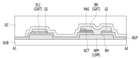
도 7은 본 발명의 실시예에 따른 픽셀을 나타낸 평면도이고, 도 8은 도 7에 도시된 제1서브 픽셀의 일부를 보다 상세히 나타낸 평면도이고, 도 9는 도 8의 일부를 더욱 상세히 나타낸 확대도이고, 도 10은 도 9에 도시된 A1-A2 영역의 단면도이고, 도 11 내지 도 14는 실시예에 따른 리페어 방법을 설명하기 위한 도면들이다.FIG. 7 is a plan view showing a pixel according to an embodiment of the present invention, FIG. 8 is a plan view showing a part of the first subpixel shown in FIG. 7 in more detail, and FIG. 9 is an enlarged view showing a part of FIG. 8 in more detail. , FIG. 10 is a cross-sectional view of the area A1-A2 shown in FIG. 9, and FIGS. 11 to 14 are drawings for explaining a repair method according to an embodiment.
도 7에 도시된 바와 같이, 제1서브 픽셀(SP1), 제2서브 픽셀(SP2), 제3서브 픽셀(SP3) 및 제4서브 픽셀(SP4)은 수직방향(제1방향)으로 배치된 두 개의 제1전원라인(EVDD), 네 개의 데이터라인(DL1~DL4), 한 개의 제1레퍼런스라인(REF1) 그리고 수평방향(제2방향)으로 배치된 한 개의 제1스캔라인(SL1)에 의해 정의될 수 있다.As shown in FIG. 7, the first subpixel SP1, the second subpixel SP2, the third subpixel SP3, and the fourth subpixel SP4 are arranged in the vertical direction (first direction). Two first power lines (EVDD), four data lines (DL1 to DL4), one first reference line (REF1), and one first scan line (SL1) arranged in the horizontal direction (second direction) It can be defined by
제1서브 픽셀(SP1), 제2서브 픽셀(SP2), 제3서브 픽셀(SP3) 및 제4서브 픽셀(SP4)은 발광영역(EMA)을 각각 포함할 수 있다. 발광영역(EMA)은 빛을 발광하는 영역으로서, 유기발광다이오드를 포함할 수 있다.The first subpixel (SP1), the second subpixel (SP2), the third subpixel (SP3), and the fourth subpixel (SP4) may each include an emission area (EMA). The light emitting area (EMA) is an area that emits light and may include an organic light emitting diode.
한편, 도 7에서는 발광영역(EMA)의 크기가 각기 다름에 따라 제1전원라인(EVDD), 제1데이터라인(DL1) 및 제2데이터라인(DL2)이 직선형을 갖지 않고 발광영역(EMA)의 주변에서 좌측으로 일부 돌출된 구조를 갖는 것을 일례로 하였으나 본 발명은 이에 한정되지 않는다. 즉, 제1서브 픽셀(SP1), 제2서브 픽셀(SP2), 제3서브 픽셀(SP3) 및 제4서브 픽셀(SP4)은 각기 다른 크기의 발광영역(EMA)을 가지며, 이에 따라 일부 라인들이 비직선형을 갖는 것을 일례로 하였으나 본 발명은 이에 한정되지 않는다.Meanwhile, in FIG. 7, as the sizes of the light emitting areas (EMA) are different, the first power line (EVDD), the first data line (DL1), and the second data line (DL2) do not have a straight line, but the light emitting areas (EMA) do not have straight lines. As an example, there is a structure that partially protrudes to the left around the periphery, but the present invention is not limited to this. That is, the first sub-pixel (SP1), the second sub-pixel (SP2), the third sub-pixel (SP3), and the fourth sub-pixel (SP4) have different sized emission areas (EMA), and accordingly, some lines Although it is an example that they have a non-linear shape, the present invention is not limited to this.
발광영역(EMA)의 하측(평면 상의 아래)에는 회로영역(또는 비발광영역)이 위치할 수 있다. 회로영역에는 구동 트랜지스터(DT), 커패시터(CST), 스위칭 트랜지스터(SW), 센싱 트랜지스터(ST)가 위치할 수 있다. 또한, 회로영역에는 수평방향으로 배치된 제1전원브래치라인(EB), 제1스캔라인(SL1), 제1레퍼런스브랜치라인(BR)과 수직방향으로 배치된 제1레퍼런스연결라인(CN)이 위치할 수 있다.A circuit area (or non-emission area) may be located below the light emitting area (EMA) (below the plane). A driving transistor (DT), a capacitor (CST), a switching transistor (SW), and a sensing transistor (ST) may be located in the circuit area. In addition, in the circuit area, a first power branch line (EB), a first scan line (SL1), and a first reference branch line (BR) arranged in the horizontal direction and a first reference connection line (CN) arranged in the vertical direction. This location can be
한편, 제1레퍼런스브랜치라인(BR)은 제1서브 픽셀(SP1), 제2서브 픽셀(SP2), 제3서브 픽셀(SP3) 및 제4서브 픽셀(SP4)에 포함된 센싱 트랜지스터(ST)와 전기적인 접속점을 가질 수 있다. 따라서, 제1레퍼런스브랜치라인(BR)은 수평방향으로만 배치되지 않고, 센싱 트랜지스터(ST)와 인접한 영역에서 수직방향으로 배치된 영역을 가질 수 있다. 또한, 제1레퍼런스브랜치라인(BR)은 주변 전극 또는 라인의 배치를 고려하여 일부 구간에 사선방향으로 배치된 영역을 가질 수 있다.Meanwhile, the first reference branch line (BR) is a sensing transistor (ST) included in the first subpixel (SP1), the second subpixel (SP2), the third subpixel (SP3), and the fourth subpixel (SP4). It may have an electrical connection point. Accordingly, the first reference branch line BR may not be arranged only horizontally, but may have a vertically arranged area in an area adjacent to the sensing transistor ST. Additionally, the first reference branch line (BR) may have an area arranged diagonally in some sections in consideration of the arrangement of peripheral electrodes or lines.
도 8 내지 도 10에 도시된 바와 같이, 회로영역에 위치하는 구동 트랜지스터(DT), 커패시터(CST), 스위칭 트랜지스터(SW), 센싱 트랜지스터(ST), 제1전원브래치라인(EB), 제1스캔라인(SL1) 및 제1레퍼런스브랜치라인(BR) 등은 하부 금속층(LSM), 반도체층(ACT), 게이트금속층(GAT), 픽셀전극층(PXL) 등을 기반으로 형성될 수 있다. 그리고 회로영역에 위치하는 전극과 전극 또는 라인과 전극은 콘택홀들(GH, PH, BH)을 통해 전기적으로 접속될 수 있다.8 to 10, the driving transistor (DT), capacitor (CST), switching transistor (SW), sensing transistor (ST), first power bracket line (EB), and The first scan line (SL1) and the first reference branch line (BR) may be formed based on a lower metal layer (LSM), a semiconductor layer (ACT), a gate metal layer (GAT), and a pixel electrode layer (PXL). And electrodes and electrodes or lines and electrodes located in the circuit area may be electrically connected through contact holes (GH, PH, BH).
GH는 게이트금속층(GAT)과 반도체층(ACT)을 전기적으로 연결하기 위한 콘택홀로 정의될 수 있고, PH는 게이트금속층(GAT)과 픽셀전극층(PXL)을 전기적으로 연결하기 위한 콘택홀로 정의될 수 있고, BH는 하부 금속층(LSM)과 게이트금속층(GAT)을 전기적으로 연결하기 위한 콘택홀로 정의될 수 있다.GH can be defined as a contact hole for electrically connecting the gate metal layer (GAT) and the semiconductor layer (ACT), and PH can be defined as a contact hole for electrically connecting the gate metal layer (GAT) and the pixel electrode layer (PXL). and BH can be defined as a contact hole for electrically connecting the lower metal layer (LSM) and the gate metal layer (GAT).
기판(SUB) 상의 회로영역에는 더미 금속층(WM)이 위치할 수 있다. 더미 금속층(WM)은 제1전원라인(EVDD) 및 하부 금속층(LSM)과 동일한 층 및 동일한 재료로 선택될 수 있다. 하부 금속층(LSM)은 구동 트랜지스터(DT)의 반도체층(ACT)으로 외부광이 유입되는 것을 차단하기 위해 형성됨은 물론이고 전극과 전극 또는 라인과 전극을 전기적으로 연결하기 위해 기판(SUB)의 바로 위에 형성되는 층일 수 있다.A dummy metal layer WM may be located in the circuit area on the substrate SUB. The dummy metal layer WM may be selected as the same layer and material as the first power line EVDD and the lower metal layer LSM. The lower metal layer (LSM) is formed not only to block external light from entering the semiconductor layer (ACT) of the driving transistor (DT), but also directly on the substrate (SUB) to electrically connect electrodes to electrodes or lines to electrodes. It may be a layer formed on top.
기판(SUB) 상에는 더미 금속층(WM)을 덮는 버퍼층(BUF)이 위치할 수 있다. 버퍼층(BUF)은 단층으로 형성된 것을 일례로 하였으나, 이는 복층으로 형성될 수도 있다. 버퍼층(BUF) 상에는 반도체층(ACT)이 위치하지 않는 영역과 반도체층(ACT)이 위치하는 영역을 포함할 수 있다. 반도체층(ACT)이 위치하지 않는 영역은 제1스캔라인(SL1)과 더미 금속층(WM)의 일단이 중첩하는 영역일 수 있고, 반도체층(ACT)이 위치하는 영역은 센싱 트랜지스터(ST)의 제1전극과 더미 금속층(WM)의 타단이 중첩하는 영역일 수 있다.A buffer layer (BUF) covering the dummy metal layer (WM) may be located on the substrate (SUB). As an example, the buffer layer (BUF) is formed as a single layer, but it may also be formed as a multiple layer. The buffer layer BUF may include a region where the semiconductor layer ACT is not located and a region where the semiconductor layer ACT is located. The area where the semiconductor layer (ACT) is not located may be an area where the first scan line (SL1) and one end of the dummy metal layer (WM) overlap, and the area where the semiconductor layer (ACT) is located is the area where the sensing transistor (ST) is located. This may be an area where the first electrode and the other end of the dummy metal layer (WM) overlap.
버퍼층(BUF) 및 센싱 트랜지스터(ST)의 반도체층(ACT) 상에는 게이트절연층(GI)이 위치할 수 있다. 게이트절연층(GI) 상에는 제1스캔라인(SL1)과 제1레퍼런스브랜치라인(BR)이 위치할 수 있다. 제1스캔라인(SL1)과 제1레퍼런스브랜치라인(BR)은 게이트금속층(GAT)에 의해 형성되지만, 패턴 공정에 의해 서로 이격됨은 물론이고 전기적으로 분리된 상태를 가질 수 있다.A gate insulating layer (GI) may be located on the buffer layer (BUF) and the semiconductor layer (ACT) of the sensing transistor (ST). A first scan line (SL1) and a first reference branch line (BR) may be located on the gate insulating layer (GI). The first scan line SL1 and the first reference branch line BR are formed by the gate metal layer GAT, but may be spaced apart from each other and electrically separated by a patterning process.
버퍼층(BUF) 상에는 게이트금속층(GAT)으로 이루어진 제1스캔라인(SL1)과 제1레퍼런스브랜치라인(BR)을 덮는 보호층(PAS)이 위치할 수 있다. 보호층(PAS) 상에는 오버코트층(또는 유기층)(OC)이 위치할 수 있다.A protective layer (PAS) covering the first scan line (SL1) and the first reference branch line (BR) made of a gate metal layer (GAT) may be located on the buffer layer (BUF). An overcoat layer (or organic layer) (OC) may be located on the protective layer (PAS).
더미 금속층(WM)의 일단은 제1스캔라인(SL1)과 중첩할 수 있지만, 더미 금속층(WM)의 일단과 제1스캔라인(SL1)은 전기적으로 분리된 상태일 수 있다. 반면, 더미 금속층(WM)의 타단은 제1레퍼런스브랜치라인(BR)과 중첩할 수 있지만, 더미 금속층(WM)의 타단과 제1레퍼런스브랜치라인(BR)은 전기적으로 연결된 상태일 수 있다. 더미 금속층(WM)의 타단은 제1레퍼런스브랜치라인(BR)에 의해 센싱 트랜지스터(ST)의 제1전극이 되는 반도체층(ACT)과 전기적으로 연결된 상태일 수 있다.One end of the dummy metal layer WM may overlap the first scan line SL1, but one end of the dummy metal layer WM and the first scan line SL1 may be electrically separated. On the other hand, the other end of the dummy metal layer (WM) may overlap the first reference branch line (BR), but the other end of the dummy metal layer (WM) and the first reference branch line (BR) may be electrically connected. The other end of the dummy metal layer (WM) may be electrically connected to the semiconductor layer (ACT), which becomes the first electrode of the sensing transistor (ST), by the first reference branch line (BR).
더미 금속층(WM)은 센싱 트랜지스터(ST)의 주변에 위치하며, 이는 웰딩(Welding) 공정에 이용되는 금속층으로 정의될 수 있다. 따라서, 더미 금속층(WM)의 일단을 통해 웰딩(Welding) 공정을 수행할 경우, 버퍼층(BUF), 게이트절연층(GI) 및 제1스캔라인(SL1)은 도 11과 같이, 용융되어 녹을 수 있다. 그리고, 제1스캔라인(SL1)과 제1레퍼런스브랜치라인(BR)은 더미 금속층(WM)에 의해 전기적으로 연결된 상태를 가질 수 있다.The dummy metal layer (WM) is located around the sensing transistor (ST), and can be defined as a metal layer used in the welding process. Therefore, when performing a welding process through one end of the dummy metal layer (WM), the buffer layer (BUF), gate insulating layer (GI), and first scan line (SL1) may melt and melt, as shown in FIG. 11. there is. Additionally, the first scan line SL1 and the first reference branch line BR may be electrically connected to each other through the dummy metal layer WM.
한편, 도 5에서 설명한 바와 같이, 더미 금속층(WM)은 제1서브 픽셀(SP1)뿐만 아니라 이와 대칭하고 있는 제4서브 픽셀(SP4)에도 위치할 수 있다. 달리 설명하면, 더미 금속층(WM)은 일측 제1전원라인(EVDD)과 제1서브 픽셀(SP1)에 포함된 센싱 트랜지스터(ST)의 사이(또는 일측 제1전원라인과 인접하는 영역) 그리고 타측 제1전원라인(EVDD)과 제4서브 픽셀(SP4)에 포함된 센싱 트랜지스터(ST)의 사이(또는 타측 제1전원라인과 인접하는 영역)에 위치할 수 있다.Meanwhile, as described in FIG. 5 , the dummy metal layer WM may be located not only in the first subpixel SP1 but also in the fourth subpixel SP4 that is symmetrical thereto. In other words, the dummy metal layer (WM) is between the first power line (EVDD) on one side and the sensing transistor (ST) included in the first sub-pixel (SP1) (or an area adjacent to the first power line on one side) and on the other side. It may be located between the first power line EVDD and the sensing transistor ST included in the fourth subpixel SP4 (or in an area adjacent to the first power line on the other side).
따라서, 도 5에서 설명한 바와 같이, 제1서브 픽셀(SP1)에 포함된 센싱 트랜지스터(ST)의 주변에 위치하는 더미 금속층(WM)은 물론이고 제4서브 픽셀(SP4)의 센싱 트랜지스터(ST)의 주변에 위치하는 더미 금속층(WM)에 대해서도 동일하게 웰딩(Welding) 공정을 수행할 수 있다.Therefore, as described in FIG. 5, the dummy metal layer WM located around the sensing transistor ST included in the first subpixel SP1 as well as the sensing transistor ST of the fourth subpixel SP4 The same welding process can be performed on the dummy metal layer WM located around .
웰딩(Welding) 공정을 수행한 후, 도 12와 같이, 제1레퍼런스라인(REF1)과 비중첩하는 제1레퍼런스연결라인(CN) 상에 라인커팅(Line Cutting) 공정을 수행할 경우, 제1레퍼런스라인(REF1)과 제1레퍼런스브랜치라인(BR)은 전기적으로 완전히 분리될 수 있다. 그 결과, 도 13 및 도 14와 같이, 제1스캔라인(SL1)과 제1레퍼런스브랜치라인(BR)은 새롭게 전기적으로 연결되고, 제1스캔라인(SL1)의 일부 구간의 단선을 리페어할 수 있는 우회 신호 패스(우회신호라인)(Path)가 마련될 수 있다.After performing the welding process, as shown in FIG. 12, when performing the line cutting process on the first reference connection line (CN) that does not overlap the first reference line (REF1), the first The reference line (REF1) and the first reference branch line (BR) can be completely electrically separated. As a result, as shown in FIGS. 13 and 14, the first scan line (SL1) and the first reference branch line (BR) are newly electrically connected, and disconnection in some sections of the first scan line (SL1) can be repaired. A bypass signal path (bypass signal line) may be provided.
도 15 및 도 16은 본 발명의 실시예에 따른 제1레퍼런스브랜치라인의 구조 그리고 그에 따른 리페어 마진을 설명하기 위한 도면들이다.Figures 15 and 16 are diagrams for explaining the structure of the first reference branch line and the resulting repair margin according to an embodiment of the present invention.
도 7, 도 15 및 도 16에 도시된 바와 같이, 제1레퍼런스브랜치라인(BR)은 제1레퍼런스연결라인(CN)을 기반으로 제1레퍼런스라인(REF1)과 전기적으로 연결될 수 있다. 제1레퍼런스브랜치라인(BR)은 제1서브 픽셀(SP1)에 접속되는 제1브랜치부분(SP1A), 제2서브 픽셀(SP2)에 접속되는 제2브랜치부분(SP2A), 제3서브 픽셀(SP3)에 접속되는 제3브랜치부분(SP3A), 제4서브 픽셀(SP4)에 접속되는 제4브랜치부분(SP4A)을 포함할 수 있다.As shown in FIGS. 7, 15, and 16, the first reference branch line (BR) may be electrically connected to the first reference line (REF1) based on the first reference connection line (CN). The first reference branch line (BR) includes a first branch part (SP1A) connected to the first subpixel (SP1), a second branch part (SP2A) connected to the second subpixel (SP2), and a third subpixel ( It may include a third branch part (SP3A) connected to SP3) and a fourth branch part (SP4A) connected to the fourth subpixel (SP4).
제2브랜치부분(SP2A)과 제3브랜치부분(SP3A)은 수평방향으로 배치될 수 있고, 각 말단에는 센싱 트랜지스터(ST)와 전기적인 접속점을 형성하기 위해 다른 영역 대비 넓은 면적을 가질 수 있다. 제2브랜치부분(SP2A)과 제3브랜치부분(SP3A)은 상호 인접하는 제2서브 픽셀(SP2)과 제3서브 픽셀(SP3)에 포함된 센싱 트랜지스터(ST)에 연결되므로 제1브랜치부분(SP1A) 및 제4브랜치부분(SP4A) 대비 짧은 배선 길이를 가질 수 있다.The second branch portion (SP2A) and the third branch portion (SP3A) may be arranged in a horizontal direction, and each end may have a larger area than other areas to form an electrical connection point with the sensing transistor (ST). The second branch portion (SP2A) and the third branch portion (SP3A) are connected to the sensing transistor (ST) included in the adjacent second sub-pixel (SP2) and third sub-pixel (SP3), so that the first branch portion ( It can have a shorter wiring length compared to SP1A) and the fourth branch part (SP4A).
제1브랜치부분(SP1A)은 제2브랜치부분(SP2A)의 중간영역으로부터 수직방향으로 연장되어 배선되고 제1서브 픽셀(SP1)이 위치하는 영역까지 수평방향으로 배선될 수 있다. 제4브랜치부분(SP4A)은 제3브랜치부분(SP3A)의 중간영역으로부터 수직방향으로 연장되어 배선되고 제4서브 픽셀(SP4)이 위치하는 영역까지 수평방향으로 배선될 수 있다. 제1브랜치부분(SP1A)과 제2브랜치부분(SP2A) 그리고 제3브랜치부분(SP3A)과 제4브랜치부분(SP4A)은 제1레퍼런스라인(REF1)을 기준으로 좌우 대칭하는 형태로 형성될 수 있다.The first branch portion SP1A may be wired to extend vertically from the middle area of the second branch part SP2A and may be wired horizontally to the area where the first subpixel SP1 is located. The fourth branch portion SP4A may be wired to extend vertically from the middle area of the third branch part SP3A and may be wired horizontally to the area where the fourth subpixel SP4 is located. The first branch part (SP1A), the second branch part (SP2A), the third branch part (SP3A), and the fourth branch part (SP4A) can be formed in a left-right symmetrical shape with respect to the first reference line (REF1). there is.
실시예에 따른 제1레퍼런스브랜치라인(BR)은 총 4개의 브랜치부분(SP1A~SP4A)을 가지고 있고, 제1레퍼런스라인(REF1)을 기준으로 좌우 대칭하는 형태로 4개의 서브커팅라인(CL1~CL4)을 형성할 수 있다. 4개의 서브커팅라인(CL1~CL4)은 4개의 서브 픽셀(SP1~SP4)에 대한 개별적인 리페어 진행시 이용될 수 있다.The first reference branch line (BR) according to the embodiment has a total of four branch parts (SP1A to SP4A) and is symmetrical left and right with respect to the first reference line (REF1) and has four subcutting lines (CL1 to SP4A). CL4) can be formed. The four subcutting lines (CL1 to CL4) can be used when performing individual repairs on the four subpixels (SP1 to SP4).
제1브랜치부분(SP1A)은 제1스캔라인(SL1)이 지나는 영역과의 사이에 제1서브커팅라인(CL1)에 대한 제1리페어 마진(RM1)을 가질 수 있다. 제2브랜치부분(SP2A)은 제1레퍼런스라인(REF1)이 지나는 영역과의 사이에 제2서브커팅라인(CL2)에 대한 제2리페어 마진(RM2)을 가질 수 있다. 그리고 제1브랜치부분(SP1A)과 제2브랜치부분(SP2A)은 제1서브커팅라인(CL1)과 제2서브커팅라인(CL2)에 의한 공유 마진(RMC)을 가질 수 있다.The first branch portion SP1A may have a first repair margin RM1 for the first subcutting line CL1 between the area through which the first scan line SL1 passes. The second branch portion SP2A may have a second repair margin RM2 for the second subcutting line CL2 between the area through which the first reference line REF1 passes. And the first branch part (SP1A) and the second branch part (SP2A) may have a shared margin (RMC) by the first sub-cutting line (CL1) and the second sub-cutting line (CL2).
제3브랜치부분(SP3A)은 제1레퍼런스라인(REF1)이 지나는 영역과의 사이에 제3서브커팅라인(CL3)에 대한 제3리페어 마진(RM3)을 가질 수 있다. 제4브랜치부분(SP4A)은 제1스캔라인(SL1)이 지나는 영역과의 사이에 제4서브커팅라인(CL4)에 대한 제4리페어 마진(RM4)을 가질 수 있다. 그리고 제3브랜치부분(SP3A)과 제4브랜치부분(SP4A)은 제3서브커팅라인(CL3)과 제4서브커팅라인(CL4)에 의한 공유 마진(RMC)을 가질 수 있다.The third branch portion SP3A may have a third repair margin RM3 for the third subcutting line CL3 between the area through which the first reference line REF1 passes. The fourth branch portion SP4A may have a fourth repair margin RM4 for the fourth subcutting line CL4 between the area through which the first scan line SL1 passes. And the third branch part (SP3A) and the fourth branch part (SP4A) may have a shared margin (RMC) by the third sub-cutting line (CL3) and the fourth sub-cutting line (CL4).
브랜치부분들(SP1A~SP4A)이 기역자(ㄱ) 형상을 이루는 영역에 형성된 공유 마진(RMC)은 제1서브커팅라인(CL1)과 제2서브커팅라인(CL2) 또는 제3서브커팅라인(CL3)과 제4서브커팅라인(CL4)을 통한 커팅 공정시 공통적으로 점유 및 공유할 수 있는 마진을 의미한다.The shared margin (RMC) formed in the area where the branch portions (SP1A to SP4A) form an inverted letter (ㄱ) shape is formed at the first sub-cutting line (CL1), the second sub-cutting line (CL2), or the third sub-cutting line (CL3). ) and the fourth sub-cutting line (CL4) refers to a margin that can be commonly occupied and shared during the cutting process.
이처럼, 브랜치부분들(SP1A~SP4A)이 공유 마진(RMC)을 갖는 경우, 다른 영역으로 리페어 마진이 확장되거나 넓은 영역을 차지하는 문제를 방지할 수 있다. 그 결과, 리페어 마진 설정에 의해 상하 인접하는 서브 픽셀들의 개구영역(또는 발광영역)이 축소되지 않고 기 설정된 개구영역을 확보(유지)할 수 있는 이점을 제공할 수 있다.In this way, when the branch parts (SP1A to SP4A) have a shared margin (RMC), the problem of the repair margin expanding to other areas or occupying a large area can be prevented. As a result, it is possible to provide the advantage of securing (maintaining) a preset aperture area without reducing the opening area (or light emitting area) of the upper and lower adjacent subpixels by setting the repair margin.
한편, 제1레퍼런스라인(REF1)과 제1레퍼런스연결라인(CN)이 중첩하는 영역은 이들 간의 전기적인 연결을 도모하기 위한 콘택홀(BH)이 형성됨에 따라 도면의 우측으로 돌출된 영역을 갖는 것을 일례로 하였으나 이는 하나의 예시로 해석되어야 한다.Meanwhile, the area where the first reference line (REF1) and the first reference connection line (CN) overlap has an area that protrudes to the right of the drawing as a contact hole (BH) is formed to facilitate electrical connection between them. Although this is an example, it should be interpreted as just one example.
도 17 및 도 18은 본 발명의 다른 실시예에 따른 스캔라인의 배치 구조를 설명하기 위한 도면들이다.Figures 17 and 18 are diagrams for explaining the arrangement structure of scan lines according to another embodiment of the present invention.
도 17 및 도 18에 도시된 바와 같이, 제1스캔라인(SL1)은 기판(SUB) 상에 위치하는 데이터라인들(DL3, DL4)을 덮고 있는 버퍼층(BUF) 그리고 버퍼층(BUF) 상의 게이트절연층(GI) 상에 위치할 수 있다. 그리고 제1스캔라인(SL1)은 보호층(PAS)과 오버코트층(OC)에 의해 보호될 수 있다.As shown in FIGS. 17 and 18, the first scan line (SL1) is a buffer layer (BUF) covering the data lines (DL3 and DL4) located on the substrate (SUB) and a gate insulation on the buffer layer (BUF). It may be located on the layer (GI). And the first scan line SL1 may be protected by a protective layer (PAS) and an overcoat layer (OC).
실시예에 따르면, 스캔라인들은 제1전원라인(EVDD)과 교차하는 브랜치 영역을 제외하고 모두 동일한 선폭을 갖도록 일자형(또는 I자형)으로 배치될 수 있다. 이는 제1스캔라인(SL1)을 참고하면 알 수 있다.According to an embodiment, the scan lines may be arranged in a straight line (or I-shape) so that all scan lines have the same line width except for the branch area that intersects the first power line EVDD. This can be seen by referring to the first scan line (SL1).
이처럼, 스캔라인들의 전반(거의 모든 구간)을 일자형(또는 I자형)으로 배치할 수 있는 이유는 스캔라인의 단선이나 스캔라인을 형성하기 위한 게이트금속층(GAT)과 다른 금속층 간의 쇼트 발생시 제1레퍼런스브랜치라인(BR) 등을 기반으로 리페어할 수 있기 때문이다. 아울러, 스캔라인들의 전반(거의 모든 구간)을 일자형(또는 I자형)으로 배치할 경우, 배선이나 전극 등의 밀집도를 더욱 증가시킬 수 있어 개구영역을 넓힐 수 있는 이점이 있다.In this way, the reason why the entire scan line (almost all sections) can be arranged in a straight line (or I-shape) is that in the event of a break in the scan line or a short circuit between the gate metal layer (GAT) to form the scan line and another metal layer, the first reference This is because repairs can be made based on branch lines (BR), etc. In addition, when the entire scan line (almost all sections) is arranged in a straight (or I-shaped) shape, the density of wiring or electrodes can be further increased, which has the advantage of widening the opening area.
이상 본 발명은 스캔라인의 단선이나 스캔라인을 형성하기 위한 게이트금속층과 다른 금속층 간의 쇼트 발생시 개구영역으로부터 이격된 영역을 웰딩하여 개구영역을 확보함과 더불어 웰딩 횟수를 최소화여 리페어 공정에 소비되는 시간을 절감할 수 있는 효과가 있다. 또한, 본 발명은 스캔라인들의 전반(거의 모든 구간)을 일자형(또는 I자형)으로 배치 가능하므로 배선이나 전극 등의 밀집도를 더욱 증가시킬 수 있고 그 결과 개구영역을 향상시킬 수 있는 효과가 있다. 또한, 본 발명은 기존 대비 단순화된 포인트 리페어 방식을 기반으로 스캔라인의 단선을 리페어할 수 있는 효과가 있다.The present invention secures the opening area by welding the area away from the opening area when a scan line is disconnected or a short circuit occurs between the gate metal layer and another metal layer to form the scan line, and the time consumed in the repair process is minimized by minimizing the number of welding operations. There is an effect of saving. In addition, the present invention can arrange the entire scan line (almost all sections) in a straight (or I-shaped) shape, so the density of wiring or electrodes can be further increased, and as a result, the opening area can be improved. In addition, the present invention has the effect of repairing disconnection of the scan line based on a point repair method that is simplified compared to the existing method.
SUB: 기판
SP1~SP4: 제1 내지 제4서브 픽셀
EVDD: 제1전원라인
ST: 센싱 트랜지스터
SL1: 스캔라인
REF1: 제1레퍼런스라인
WM: 더미 금속층
BR: 레퍼런스브랜치라인
BUF: 버퍼층
GI: 게이트절연층
GAT: 게이트금속층
PAS: 보호층SUB: Substrate SP1 to SP4: First to fourth subpixels
EVDD: 1st power line ST: Sensing transistor
SL1: Scan line REF1: First reference line
WM: Dummy metal layer BR: Reference branch line
BUF: buffer layer GI: gate insulation layer
GAT: Gate metal layer PAS: Protection layer
Claims (13)
상기 기판 상에 제1방향으로 배치된 레퍼런스라인;
상기 기판 상에 상기 제1방향으로 배치된 전원라인;
상기 기판 상에 상기 제1방향과 교차하는 제2방향으로 배치된 스캔라인;
상기 레퍼런스라인에 연결되고 상기 제2방향으로 배치된 레퍼런스브랜치라인; 및
상기 기판 상에 위치하며 상기 스캔라인과 중첩하는 영역과 상기 레퍼런스브랜치라인과 중첩하는 영역을 갖는 더미 금속층을 포함하는 발광표시장치.A plurality of subpixels located on a substrate;
a reference line disposed in a first direction on the substrate;
a power line disposed in the first direction on the substrate;
a scan line disposed on the substrate in a second direction intersecting the first direction;
a reference branch line connected to the reference line and disposed in the second direction; and
A light emitting display device comprising a dummy metal layer located on the substrate and having an area overlapping the scan line and an area overlapping the reference branch line.
상기 더미 금속층은 상기 기판 상의 바로 위에 위치하는 하부 금속층으로 선택되고,
상기 스캔라인과 상기 레퍼런스브랜치라인은 상기 하부 금속층보다 상층에 위치하는 게이트금속층으로 선택되는 발광표시장치.According to paragraph 1,
The dummy metal layer is selected as a lower metal layer located immediately above the substrate,
The scan line and the reference branch line are selected from a gate metal layer located above the lower metal layer.
상기 더미 금속층은
상기 스캔라인과 전기적으로 분리된 상태를 갖고, 상기 레퍼런스브랜치라인과 전기적으로 연결된 상태를 갖는 발광표시장치.According to paragraph 1,
The dummy metal layer is
A light emitting display device electrically separated from the scan line and electrically connected to the reference branch line.
상기 더미 금속층은
웰딩 공정에 의해 상기 스캔라인과 전기적으로 연결된 상태를 갖는 발광표시장치.According to paragraph 1,
The dummy metal layer is
A light emitting display device electrically connected to the scan line through a welding process.
상기 더미 금속층과 상기 스캔라인이 전기적으로 연결된 상태를 갖는 경우,
상기 레퍼런스라인과 상기 레퍼런스브랜치라인은 전기적으로 분리된 상태를 갖는 발광표시장치.According to clause 4,
When the dummy metal layer and the scan line are electrically connected,
A light emitting display device in which the reference line and the reference branch line are electrically separated.
상기 더미 금속층과 상기 스캔라인이 전기적으로 연결되고, 상기 레퍼런스라인과 상기 레퍼런스브랜치라인이 전기적으로 분리된 상태를 갖는 경우,
상기 레퍼런스브랜치라인은 상기 스캔라인을 통해 인가되는 스캔신호를 우회하여 전달하는 우회신호라인으로 기능하는 발광표시장치.According to clause 5,
When the dummy metal layer and the scan line are electrically connected, and the reference line and the reference branch line are electrically separated,
The reference branch line is a light emitting display device that functions as a bypass signal line that bypasses and transmits the scan signal applied through the scan line.
상기 더미 금속층은
상기 전원라인과 인접하는 영역에 배치된 발광표시장치.According to paragraph 1,
The dummy metal layer is
A light emitting display device disposed in an area adjacent to the power line.
상기 스캔라인은
상기 전원라인과 교차하는 영역을 제외하고 일자형(또는 I자형)으로 배치된 발광표시장치.According to paragraph 1,
The scan line is
A light emitting display device arranged in a straight line (or I-shape) except for the area intersecting the power line.
상기 레퍼런스브랜치라인은
상기 제1방향으로 배치된 레퍼런스연결라인에 의해 상기 레퍼런스라인에 전기적으로 연결되고,
상기 레퍼런스브랜치라인이 상기 우회신호라인으로 기능할 경우, 상기 레퍼런스연결라인은 라인커팅 공정에 의해 상기 레퍼런스라인으로부터 전기적으로 분리된 상태를 갖는 발광표시장치.According to clause 6,
The reference branch line is
electrically connected to the reference line by a reference connection line disposed in the first direction,
When the reference branch line functions as the bypass signal line, the reference connection line is electrically separated from the reference line by a line cutting process.
상기 레퍼런스브랜치라인은
제1서브 픽셀에 접속되는 제1브랜치부분과,
상기 제1서브 픽셀에 인접하는 제2서브 픽셀에 접속되는 제2브랜치부분과,
상기 제2서브 픽셀에 인접하는 제3서브 픽셀에 접속되는 제3브랜치부분과,
상기 제3서브 픽셀에 인접하는 제4서브 픽셀에 접속되는 제4브랜치부분을 포함하는 발광표시장치.According to paragraph 1,
The reference branch line is
A first branch portion connected to the first subpixel,
a second branch portion connected to a second sub-pixel adjacent to the first sub-pixel;
a third branch portion connected to a third sub-pixel adjacent to the second sub-pixel;
A light emitting display device comprising a fourth branch portion connected to a fourth sub-pixel adjacent to the third sub-pixel.
상기 제2브랜치부분과 상기 제3브랜치부분은 상기 제1방향으로 배치되고,
상기 제1브랜치부분은 상기 제2브랜치부분의 중간영역으로부터 수직방향으로 연장되어 배선되고 상기 제1서브 픽셀이 위치하는 영역까지 수평방향으로 배선되고,
상기 제4브랜치부분은 상기 제3브랜치부분의 중간영역으로부터 수직방향으로 연장되어 배선되고 상기 제4서브 픽셀이 위치하는 영역까지 수평방향으로 배선된 발광표시장치.According to clause 10,
The second branch portion and the third branch portion are arranged in the first direction,
The first branch portion is wired to extend vertically from the middle area of the second branch portion and is wired horizontally to the area where the first sub-pixel is located,
The fourth branch portion is wired to extend vertically from the middle area of the third branch portion and is wired horizontally to the area where the fourth sub-pixel is located.
상기 제1브랜치부분과 상기 제2브랜치부분 그리고 상기 제3브랜치부분과 상기 제4브랜치부분은 상기 레퍼런스라인을 기준으로 좌우 대칭하는 발광표시장치.According to clause 11,
A light emitting display device wherein the first branch portion, the second branch portion, the third branch portion, and the fourth branch portion are left and right symmetrical with respect to the reference line.
상기 스캔라인의 일측과 상기 레퍼런스브랜치라인의 일측이 전기적으로 연결되고 상기 스캔라인의 타측과 상기 레퍼런스브랜치라인의 타측이 전기적으로 연결되도록 상기 스캔라인의 단선 구간 주변에 위치하는 일측 서브 픽셀의 더미 금속층과 상기 일측 서브 픽셀로부터 이격된 타측 서브 픽셀의 더미 금속층을 웰딩하는 단계; 및
상기 레퍼런스라인과 상기 레퍼런스브랜치라인이 전기적으로 분리되도록 커팅하는 단계를 포함하는 발광표시장치의 리페어 방법.In the repair method of a light emitting display device manufactured according to any one of claims 1 to 12,
A dummy metal layer of one sub-pixel located around a disconnection section of the scan line so that one side of the scan line and one side of the reference branch line are electrically connected and the other side of the scan line and the other side of the reference branch line are electrically connected. and welding a dummy metal layer of the other subpixel spaced apart from the one subpixel; and
A repair method for a light emitting display device comprising the step of cutting the reference line and the reference branch line to electrically separate them.
Priority Applications (3)
| Application Number | Priority Date | Filing Date | Title |
|---|---|---|---|
| KR1020220079653A KR20240002442A (en) | 2022-06-29 | 2022-06-29 | Light emitting display device and repair method of the same |
| US18/206,641 US12288521B2 (en) | 2022-06-29 | 2023-06-07 | Light emitting display apparatus and method of repairing the same |
| CN202310747829.7A CN117320497A (en) | 2022-06-29 | 2023-06-21 | Display panel and repair method thereof, light-emitting display device including display panel |
Applications Claiming Priority (1)
| Application Number | Priority Date | Filing Date | Title |
|---|---|---|---|
| KR1020220079653A KR20240002442A (en) | 2022-06-29 | 2022-06-29 | Light emitting display device and repair method of the same |
Publications (1)
| Publication Number | Publication Date |
|---|---|
| KR20240002442A true KR20240002442A (en) | 2024-01-05 |
Family
ID=89241452
Family Applications (1)
| Application Number | Title | Priority Date | Filing Date |
|---|---|---|---|
| KR1020220079653A Pending KR20240002442A (en) | 2022-06-29 | 2022-06-29 | Light emitting display device and repair method of the same |
Country Status (3)
| Country | Link |
|---|---|
| US (1) | US12288521B2 (en) |
| KR (1) | KR20240002442A (en) |
| CN (1) | CN117320497A (en) |
Families Citing this family (1)
| Publication number | Priority date | Publication date | Assignee | Title |
|---|---|---|---|---|
| KR20240100933A (en) * | 2022-12-23 | 2024-07-02 | 엘지디스플레이 주식회사 | Display device and display panel |
Family Cites Families (3)
| Publication number | Priority date | Publication date | Assignee | Title |
|---|---|---|---|---|
| KR102157894B1 (en) * | 2014-03-11 | 2020-09-22 | 삼성디스플레이 주식회사 | Liquid crystal display panel |
| KR102885297B1 (en) * | 2019-01-11 | 2025-11-12 | 삼성디스플레이 주식회사 | Organic light emitting display device |
| KR102656012B1 (en) * | 2019-03-19 | 2024-04-11 | 삼성전자주식회사 | Led display panel and repairing method |
-
2022
- 2022-06-29 KR KR1020220079653A patent/KR20240002442A/en active Pending
-
2023
- 2023-06-07 US US18/206,641 patent/US12288521B2/en active Active
- 2023-06-21 CN CN202310747829.7A patent/CN117320497A/en active Pending
Also Published As
| Publication number | Publication date |
|---|---|
| CN117320497A (en) | 2023-12-29 |
| US12288521B2 (en) | 2025-04-29 |
| US20240005865A1 (en) | 2024-01-04 |
Similar Documents
| Publication | Publication Date | Title |
|---|---|---|
| JP3608614B2 (en) | Display device | |
| JP5971735B2 (en) | Organic light emitting display device repair method | |
| KR102123979B1 (en) | Organic light emitting display device having repair structure | |
| US20220069044A1 (en) | Display device | |
| KR102592010B1 (en) | Display apparatus | |
| KR20180035966A (en) | Display device | |
| CN110571238B (en) | Organic light emitting display panel and organic light emitting display device including same | |
| CN113724651A (en) | Array substrate and display panel | |
| US11818929B2 (en) | Display device with repair patterns | |
| KR20240002442A (en) | Light emitting display device and repair method of the same | |
| KR20220095451A (en) | Display device | |
| KR20220086860A (en) | Light emitting display apparatus | |
| KR20230101011A (en) | Display device | |
| KR20240002447A (en) | Light emitting display device and repair method of the same | |
| KR102089336B1 (en) | Organic Light Emitting Display Device | |
| KR102937610B1 (en) | Light emitting display device | |
| KR102913454B1 (en) | Light Emitting Display Device | |
| JP2012104497A (en) | Display device | |
| KR102670408B1 (en) | Display Device | |
| KR102885780B1 (en) | Display device | |
| US20240074285A1 (en) | Display device and method for repairing the same | |
| KR102840211B1 (en) | Light emitting display device | |
| JP5179806B2 (en) | Display device | |
| KR102618594B1 (en) | Display Device and Manufacturing Method of the same | |
| KR20240106135A (en) | Display device |
Legal Events
| Date | Code | Title | Description |
|---|---|---|---|
| PA0109 | Patent application |
St.27 status event code: A-0-1-A10-A12-nap-PA0109 |
|
| P22-X000 | Classification modified |
St.27 status event code: A-2-2-P10-P22-nap-X000 |
|
| P22-X000 | Classification modified |
St.27 status event code: A-2-2-P10-P22-nap-X000 |
|
| PG1501 | Laying open of application |
St.27 status event code: A-1-1-Q10-Q12-nap-PG1501 |
|
| A201 | Request for examination | ||
| D21 | Rejection of application intended |
Free format text: ST27 STATUS EVENT CODE: A-1-2-D10-D21-EXM-PE0902 (AS PROVIDED BY THE NATIONAL OFFICE) |
|
| PE0902 | Notice of grounds for rejection |
St.27 status event code: A-1-2-D10-D21-exm-PE0902 |