KR20230144470A - Semiconductor apparatus and semicondcutor system having independent data input/output period, and an operating method of the semiconductor system - Google Patents
Semiconductor apparatus and semicondcutor system having independent data input/output period, and an operating method of the semiconductor system Download PDFInfo
- Publication number
- KR20230144470A KR20230144470A KR1020230038593A KR20230038593A KR20230144470A KR 20230144470 A KR20230144470 A KR 20230144470A KR 1020230038593 A KR1020230038593 A KR 1020230038593A KR 20230038593 A KR20230038593 A KR 20230038593A KR 20230144470 A KR20230144470 A KR 20230144470A
- Authority
- KR
- South Korea
- Prior art keywords
- command
- semiconductor device
- data
- memory die
- address signal
- Prior art date
- Legal status (The legal status is an assumption and is not a legal conclusion. Google has not performed a legal analysis and makes no representation as to the accuracy of the status listed.)
- Pending
Links
Images


Classifications
-
- G—PHYSICS
- G11—INFORMATION STORAGE
- G11C—STATIC STORES
- G11C16/00—Erasable programmable read-only memories
- G11C16/02—Erasable programmable read-only memories electrically programmable
- G11C16/06—Auxiliary circuits, e.g. for writing into memory
- G11C16/08—Address circuits; Decoders; Word-line control circuits
-
- G—PHYSICS
- G06—COMPUTING OR CALCULATING; COUNTING
- G06F—ELECTRIC DIGITAL DATA PROCESSING
- G06F13/00—Interconnection of, or transfer of information or other signals between, memories, input/output devices or central processing units
- G06F13/14—Handling requests for interconnection or transfer
- G06F13/20—Handling requests for interconnection or transfer for access to input/output bus
-
- G—PHYSICS
- G06—COMPUTING OR CALCULATING; COUNTING
- G06F—ELECTRIC DIGITAL DATA PROCESSING
- G06F13/00—Interconnection of, or transfer of information or other signals between, memories, input/output devices or central processing units
- G06F13/14—Handling requests for interconnection or transfer
- G06F13/16—Handling requests for interconnection or transfer for access to memory bus
- G06F13/1605—Handling requests for interconnection or transfer for access to memory bus based on arbitration
- G06F13/1652—Handling requests for interconnection or transfer for access to memory bus based on arbitration in a multiprocessor architecture
-
- G—PHYSICS
- G06—COMPUTING OR CALCULATING; COUNTING
- G06F—ELECTRIC DIGITAL DATA PROCESSING
- G06F13/00—Interconnection of, or transfer of information or other signals between, memories, input/output devices or central processing units
- G06F13/14—Handling requests for interconnection or transfer
- G06F13/16—Handling requests for interconnection or transfer for access to memory bus
- G06F13/1668—Details of memory controller
-
- G—PHYSICS
- G11—INFORMATION STORAGE
- G11C—STATIC STORES
- G11C16/00—Erasable programmable read-only memories
- G11C16/02—Erasable programmable read-only memories electrically programmable
- G11C16/06—Auxiliary circuits, e.g. for writing into memory
- G11C16/10—Programming or data input circuits
-
- G—PHYSICS
- G11—INFORMATION STORAGE
- G11C—STATIC STORES
- G11C16/00—Erasable programmable read-only memories
- G11C16/02—Erasable programmable read-only memories electrically programmable
- G11C16/06—Auxiliary circuits, e.g. for writing into memory
- G11C16/32—Timing circuits
-
- G—PHYSICS
- G11—INFORMATION STORAGE
- G11C—STATIC STORES
- G11C7/00—Arrangements for writing information into, or reading information out from, a digital store
- G11C7/10—Input/output [I/O] data interface arrangements, e.g. I/O data control circuits, I/O data buffers
- G11C7/1048—Data bus control circuits, e.g. precharging, presetting, equalising
Landscapes
- Engineering & Computer Science (AREA)
- Theoretical Computer Science (AREA)
- Physics & Mathematics (AREA)
- General Engineering & Computer Science (AREA)
- General Physics & Mathematics (AREA)
- Dram (AREA)
Abstract
Description
본 발명은 집적 회로 기술에 관한 것으로, 더 상세하게는 데이터 입출력 구간을 갖는 반도체 장치 및 반도체 시스템에 관한 것이다. The present invention relates to integrated circuit technology, and more specifically to semiconductor devices and semiconductor systems having data input/output sections.
전자장치는 많은 전자 구성요소를 포함하고 있고, 그 중 컴퓨터 시스템은 반도체로 구성된 많은 반도체 장치들을 포함할 수 있다. 컴퓨터 시스템을 구성하는 반도체 장치들은 마스터 장치로 동작하는 프로세서 또는 메모리 컨트롤러와 슬레이브 장치로 동작하는 메모리 장치 또는 스토리지 장치를 포함할 수 있다. 상기 마스터 장치는 상기 슬레이브 장치로 커맨드 어드레스 신호를 제공할 수 있고, 상기 슬레이브 장치는 상기 커맨드 어드레스 신호에 기초하여 다양한 동작을 수행할 수 있다. 또한, 상기 마스터 장치 및 상기 슬레이브 장치는 서로 데이터를 전송 및 수신할 수 있다. Electronic devices include many electronic components, and among them, computer systems may include many semiconductor devices made of semiconductors. Semiconductor devices constituting a computer system may include a processor or memory controller operating as a master device and a memory device or storage device operating as a slave device. The master device can provide a command address signal to the slave device, and the slave device can perform various operations based on the command address signal. Additionally, the master device and the slave device can transmit and receive data from each other.
낸드 플래시 메모리 시스템에서 낸드 플래시 메모리 장치는 메모리 컨트롤러와 다양한 인터페이스 방식으로 통신을 수행할 수 있다. 낸드 인터페이스 방식은 커맨드 어드레스 신호와 데이터가 동일한 입출력 버스를 통해 전송될 수 있다. 낸드 플래시 메모리 시스템의 동작 주파수가 상승하면서, 상기 낸드 인터페이스 방식은 커맨드 오버헤드(command overhead)가 증가하여 메모리 시스템의 성능 저하를 발생시킬 수 있다. SCA (Serial Command Address) 인터페이스 방식은 커맨드 어드레스 신호와 데이터가 서로 다른 입출력 버스를 통해 전송될 수 있다. 상기 SCA 인터페이스 방식은 상기 커맨드 오버헤드를 일부 감소시킬 수 있지만 복수의 낸드 플래시 메모리 장치의 동작이 병렬적으로 수행되기 어렵다.In a NAND flash memory system, a NAND flash memory device can communicate with a memory controller through various interface methods. In the NAND interface method, command address signals and data can be transmitted through the same input/output bus. As the operating frequency of the NAND flash memory system increases, the command overhead of the NAND interface method increases, which may cause performance degradation of the memory system. The SCA (Serial Command Address) interface method allows command address signals and data to be transmitted through different input/output buses. Although the SCA interface method can partially reduce the command overhead, it is difficult for the operations of a plurality of NAND flash memory devices to be performed in parallel.
본 발명의 실시 예는 독립적인 데이터 입출력 구간을 정의하는 커맨드 어드레스 신호를 사용하는 반도체 장치, 반도체 시스템 및 반도체 시스템의 동작 방법을 제공할 수 있다.Embodiments of the present invention can provide a semiconductor device, a semiconductor system, and a method of operating the semiconductor system using a command address signal that defines an independent data input/output section.
본 발명의 실시 예에 따른 반도체 시스템은 칩 인에이블 신호 및 제 1 커맨드 어드레스 신호 세트를 제공한 후 데이터 입출력 구간을 정의하는 제 2 커맨드 어드레스 신호 세트를 제공하는 제 1 반도체 장치; 및 상기 칩 인에이블 신호 및 상기 제 1 커맨드 어드레스 신호 세트에 기초하여 내부 동작을 수행하고, 상기 제 2 커맨드 어드레스 신호 세트에 기초하여 데이터 버스를 통해 상기 제 1 반도체 장치와 연결되는 제 2 반도체 장치를 포함할 수 있다.A semiconductor system according to an embodiment of the present invention includes a first semiconductor device that provides a chip enable signal and a first command address signal set and then provides a second command address signal set defining a data input/output section; and a second semiconductor device that performs an internal operation based on the chip enable signal and the first command address signal set and is connected to the first semiconductor device through a data bus based on the second command address signal set. It can be included.
본 발명의 실시 예에 따른 반도체 시스템의 동작 방법은 제 1 반도체 장치에 의해 데이터 입력 커맨드 및 데이터 출력 커맨드 중 하나와 칩 인에이블 신호를 상기 제 2 반도체 장치로 제공하는 단계; 제 2 반도체 장치에 의해 상기 칩 인에이블 신호 및 제 1 커맨드 어드레스 신호 세트에 기초하여 내부 동작을 수행하는 단계; 상기 제 1 반도체 장치에 의해 선택 칩 인에이블 커맨드를 상기 제 2 반도체 장치로 제공하는 단계; 및 상기 제 1 반도체 장치에 의해 데이터를 상기 제 2 반도체 장치로 전송하거나, 상기 제 2 반도체 장치에 의해 상기 데이터를 상기 제 1 반도체 장치로 전송하는 단계를 포함할 수 있다.A method of operating a semiconductor system according to an embodiment of the present invention includes providing, by a first semiconductor device, one of a data input command and a data output command and a chip enable signal to the second semiconductor device; performing an internal operation based on the chip enable signal and the first command address signal set by a second semiconductor device; providing a select chip enable command to the second semiconductor device by the first semiconductor device; and transmitting the data to the second semiconductor device by the first semiconductor device, or transmitting the data to the first semiconductor device by the second semiconductor device.
본 발명의 실시 예에 따른 반도체 시스템은 제 1 칩 인에이블 신호, 제 2 칩 인에이블 신호, 제 1 커맨드 어드레스 신호 세트, 제 2 커맨드 어드레스 신호 세트 및 제 3 커맨드 어드레스 신호 세트를 제공하고, 데이터 버스와 연결되는 반도체 장치; 상기 제 1 칩 인에이블 신호 및 상기 제 1 커맨드 어드레스 신호 세트에 기초하여 내부 동작을 수행하고, 상기 제 2 커맨드 어드레스 신호 세트에 기초하여 상기 데이터 버스와 연결되는 1 메모리 다이; 및 상기 제 2 칩 인에이블 신호 및 상기 제 1 커맨드 어드레스 신호 세트에 기초하여 내부 동작을 수행하고, 상기 제 3 커맨드 어드레스 신호 세트에 기초하여 상기 데이터 버스와 연결되는 제 2 메모리 다이를 포함할 수 있다.A semiconductor system according to an embodiment of the present invention provides a first chip enable signal, a second chip enable signal, a first command address signal set, a second command address signal set, and a third command address signal set, and a data bus. a semiconductor device connected to; one memory die that performs an internal operation based on the first chip enable signal and the first command address signal set and is connected to the data bus based on the second command address signal set; and a second memory die that performs an internal operation based on the second chip enable signal and the first command address signal set and is connected to the data bus based on the third command address signal set. .
본 발명의 실시 예에 따른 반도체 시스템의 동작 방법은 반도체 장치에 의해 제 1 메모리 다이로 제 1 칩 인에이블 신호 및 커맨드를 어드레스 신호 세트를 제공하는 단계; 상기 반도체 장치에 의해 상기 제 1 메모리 다이로 제 1 선택 칩 인에이블 커맨드를 제공하는 단계; 상기 반도체 장치에 의해 상기 제 1 메모리 다이로부터 데이터를 수신하거나 상기 제 1 메모리 다이로 상기 데이터를 전송하는 단계; 및 상기 반도체 장치에 의해 상기 제 1 메모리 다이로 제 1 선택 칩 디스에이블 커맨드 및 제 1 선택 칩 종료 커맨드 중 하나를 제공하는 단계를 포함할 수 있다.A method of operating a semiconductor system according to an embodiment of the present invention includes providing a first chip enable signal and a command address signal set to a first memory die by a semiconductor device; providing a first select chip enable command to the first memory die by the semiconductor device; receiving data from or transmitting the data to the first memory die by the semiconductor device; and providing one of a first selected chip disable command and a first selected chip end command to the first memory die by the semiconductor device.
본 발명의 실시 예는 복수의 다이의 인터리브드 (interleaved) 동작을 가능하게 하여 반도체 시스템의 성능을 향상시킬 수 있다. Embodiments of the present invention can improve the performance of a semiconductor system by enabling interleaved operation of a plurality of dies.
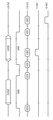
도 1은 본 발명의 실시 예에 따른 반도체 시스템의 구성을 보여주는 도면이다.
도 2a는 본 발명의 실시 예에 따른 반도체 시스템의 동작을 보여주는 도면이다.
도 2b는 본 발명의 실시 예에 따른 반도체 시스템의 동작을 보여주는 도면이다.
도 3a는 본 발명의 실시 예에 따른 반도체 시스템의 동작을 보여주는 도면이다.
도 3b는 본 발명의 실시 예에 따른 반도체 시스템의 동작을 보여주는 도면이다.
도 4는 본 발명의 실시 예에 따른 반도체 시스템의 동작을 보여주는 도면이다.
도 5는 본 발명의 실시 예에 따른 반도체 시스템의 동작을 보여주는 도면이다.
도 6은 본 발명의 실시 예에 따른 커맨드 어드레스 신호의 구성을 보여주는 도면이다.
도 7은 본 발명의 실시 예에 따른 커맨드 어드레스 신호 세트를 보여주는 테이블이다.
도 8a는 본 발명의 실시 예에 따른 선택 칩 인에이블 커맨드의 구성을 예시적으로 보여주는 도면이다.
도 8b는 본 발명의 실시 예에 따른 선택 칩 디스에이블 커맨드의 구성을 예시적으로 보여주는 도면이다.1 is a diagram showing the configuration of a semiconductor system according to an embodiment of the present invention.
FIG. 2A is a diagram showing the operation of a semiconductor system according to an embodiment of the present invention.
Figure 2b is a diagram showing the operation of a semiconductor system according to an embodiment of the present invention.
FIG. 3A is a diagram showing the operation of a semiconductor system according to an embodiment of the present invention.
Figure 3b is a diagram showing the operation of a semiconductor system according to an embodiment of the present invention.
Figure 4 is a diagram showing the operation of a semiconductor system according to an embodiment of the present invention.
5 is a diagram showing the operation of a semiconductor system according to an embodiment of the present invention.
Figure 6 is a diagram showing the configuration of a command address signal according to an embodiment of the present invention.
Figure 7 is a table showing a command address signal set according to an embodiment of the present invention.
FIG. 8A is a diagram illustrating the configuration of a select chip enable command according to an embodiment of the present invention.
FIG. 8B is a diagram illustrating the configuration of a select chip disable command according to an embodiment of the present invention.
도 1은 본 발명의 실시 예에 따른 반도체 시스템(1)의 구성을 보여주는 도면이다. 도 1에서, 상기 반도체 시스템(1)은 제 1 반도체 장치(110) 및 제 2 반도체 장치(120)를 포함할 수 있다. 상기 제 1 반도체 장치(110)는 상기 제 2 반도체 장치(120)가 동작하는데 사용되는 다양한 제어 신호를 제공할 수 있다. 상기 제 1 반도체 장치(110)는 다양한 종류의 마스터 장치를 포함할 수 있다. 예를 들어, 상기 제 1 반도체 장치(110)는 중앙처리장치(CPU), 그래픽 처리 장치(Graphic Processing Unit, GPU), 멀티미디어 프로세서(Multi-Media Processor, MMP), 디지털 신호 프로세서(Digital Signal Processor), 어플리케이션 프로세서(AP) 및 메모리 컨트롤러와 같은 호스트 장치일 수 있다. 상기 제 2 반도체 장치(120)는 상기 제 1 반도체 장치(110)의 제어에 따라 다양한 동작을 수행하는 슬레이브 장치일 수 있고, 예를 들어, 메모리 장치일 수 있다. 상기 메모리 장치는 휘발성 메모리와 비휘발성 메모리를 포함할 수 있다. 상기 휘발성 메모리는 SRAM (Static RAM), DRAM (Dynamic RAM), SDRAM (Synchronous DRAM)을 포함할 수 있고, 상기 비휘발성 메모리는 ROM (Read Only Memory), PROM (Programmable ROM), EEPROM (Electrically Erase and Programmable ROM), EPROM (Electrically Programmable ROM), 플래시 메모리, PRAM (Phase change RAM), MRAM (Magnetic RAM), RRAM (Resistive RAM) 및 FRAM (Ferroelectric RAM) 등을 포함할 수 있다.1 is a diagram showing the configuration of a
상기 제 1 반도체 장치(110)는 복수의 버스를 통해 상기 제 2 반도체 장치(120)와 연결될 수 있다. 상기 복수의 버스는 신호를 전송하기 위한 신호 전송 경로, 링크 또는 채널일 수 있다. 상기 복수의 버스는 커맨드 어드레스 버스(101), 칩 인에이블 버스(102), 커맨드 클럭 버스(103) 및 데이터 버스(104)상기 커맨드 어드레스 버스(101), 상기 칩 인에이블 버스(102) 및 상기 클럭 커맨드 버스(103)는 상기 제 1 반도체 장치(110)로부터 상기 제 2 반도체 장치(120)로의 단방향 버스일 수 있고, 상기 데이터 버스(104)는 양방향 버스일 수 있다. 상기 제 1 반도체 장치(110)는 상기 커맨드 어드레스 버스(101)를 통해 커맨드 어드레스 신호(CA<0:1>)를 상기 제 2 반도체 장치(120)로 제공할 수 있다. 상기 제 1 반도체 장치(110)가 전송하는 상기 커맨드 어드레스 신호(CA<0:1>)는 커맨드 신호 및 어드레스 신호를 포함할 수 있다. 상기 커맨드 신호는 상기 제 2 반도체 장치(120)가 수행하는 동작을 특정하는 커맨드 정보를 포함할 수 있다. 상기 어드레스 신호(ADD)는 상기 제 2 반도체 장치(120)의 저장 영역을 액세스하기 위한 주소 정보를 포함할 수 있다. 예를 들어, 상기 커맨드 신호는 데이터 입력 커맨드, 데이터 출력 커맨드, 선택 칩 인에이블 커맨드 및 선택 칩 디스에이블 커맨드를 포함할 수 있다. 일 실시 예에서, 상기 커맨드 신호는 선택 칩 종료 커맨드를 더 포함할 수 있다. 상기 제 1 반도체 장치(110)는 상기 커맨드 어드레스 버스(101)를 통해 단위 사이클마다 2비트의 상기 커맨드 어드레스 신호(CA<0:1>)를 상기 제 2 반도체 장치(120)로 전송할 수 있다. 복수의 사이클 동안 전송되는 상기 커맨드 어드레스 신호들(CA<0:1>)이 하나의 커맨드 어드레스 신호 세트를 구성할 수 있다. 상기 제 1 반도체 장치(110)는 상기 칩 인에이블 버스(102)를 통해 상기 제 2 반도체 장치(120)로 칩 인에이블 신호(CE#<0:1>)를 전송할 수 있다. 도 1에서, 상기 칩 인에이블 신호는 2비트를 포함하는 것으로 도시되었지만, 상기 제 2 반도체 장치(120)가 포함하는 메모리 다이 또는 메모리 칩의 개수에 따라, 상기 칩 인에이블 신호(CE#<0:1>)의 비트의 개수는 변경될 수 있을 것이다. 예를 들어, 상기 제 2 반도체 장치(110)가 2개의 메모리 다이 또는 메모리 칩을 포함할 때, 상기 제 1 반도체 장치(120)는 제 1 칩 인에이블 신호(CE#<0>) 및 제 2 칩 인에이블 신호(CE#<1>)를 상기 칩 인에이블 버스(102)를 통해 상기 제 2 반도체 장치(120)로 제공할 수 있다. 상기 제 1 및 제 2 칩 인에이블 신호(CE#<0>, CE#<1>)는 상기 커맨드 어드레스 신호(CA<0:1>)와 함께 제공될 수 있다. 예를 들어, 상기 제 1 반도체 장치(110)는 상기 제 2 반도체 장치(120)의 제 1 메모리 다이(DIE1)를 동작시키기 위해 상기 커맨드 어드레스 신호(CA<0:1>)와 상기 제 1 칩 인에이블 신호(CE#<0>)를 함께 제공할 수 있다. 상기 제 1 반도체 장치(110)는 상기 제 2 반도체 장치(120)의 제 2 메모리 다이(DIE2)를 동작시키기 위해 상기 커맨드 어드레스 신호(CA<0:1>)와 상기 제 2 칩 인에이블 신호(CE#<1>)를 함께 전송할 수 있다. The
상기 제 1 반도체 장치(110)는 상기 커맨드 클럭 버스(103)를 통해 커맨드 클럭 신호(CCK)를 상기 제 2 반도체 장치(120)로 제공할 수 있다. 상기 커맨드 클럭 버스(103)는 상기 커맨드 어드레스 신호(CA<0:1>)와 동기되는 신호로서 상기 제 2 반도체 장치(120)가 상기 커맨드 어드레스 신호(CA<0:1>)를 유효한 신호로서 수신하는 구간을 정의하는 신호일 수 있다. 예를 들어, 상기 커맨드 클럭 신호(CCK)가 토글하는 구간에서 상기 제 2 반도체 장치(120)는 상기 제 1 반도체 장치(110)로부터 전송된 상기 커맨드 어드레스 신호(CA<0:1>)를 유효한 신호로 샘플링할 수 있다. 상기 제 1 반도체 장치(110)는 상기 데이터 버스(104)를 통해 상기 제 2 반도체 장치(120)로 데이터(DQ<0:7>)를 제공하거나 상기 제 2 반도체 장치(120)로부터 상기 데이터(DQ<0:7>)를 수신할 수 있다. 상기 제 1 반도체 장치(110)로부터 상기 제 2 반도체 장치(120)로 상기 데이터(DQ<0:7>)가 전송되는 동작은 데이터 입력 동작일 수 있고, 상기 제 2 반도체 장치(120)로부터 상기 제 1 반도체 장치(110)로 상기 데이터(DQ<0:7>)가 전송되는 동작은 데이터 출력 동작일 수 있다. The
상기 제 1 반도체 장치(110)는 커맨드 어드레스 생성 회로(111) 및 데이터 입출력 회로(112)를 포함할 수 있다. 상기 커맨드 어드레스 생성 회로(111)는 사용자의 리퀘스트(REQ)에 기초하여 상기 커맨드 어드레스 신호(CA<0:1>) 및 상기 칩 인에이블 신호(CE#<0:1>)를 생성할 수 있다. 상기 커맨드 어드레스 생성 회로(111)는 상기 커맨드 어드레스 신호(CA<0:1>)를 상기 커맨드 어드레스 버스(101)를 통해 상기 제 2 반도체 장치(120)로 전송하고, 상기 칩 인에이블 버스(102)를 통해 상기 칩 인에이블 신호(CE#<0:1>)를 상기 제 2 반도체 장치(120)로 전송할 수 있다. 상기 커맨드 어드레스 생성 회로(111)는 상기 커맨드 어드레스 신호 세트의 길이 및/또는 총 비트 수에 따라 복수의 사이클 동안 상기 커맨드 어드레스 신호(CA<0:1>)를 상기 제 2 반도체 장치(120)로 전송할 수 있다. 상기 커맨드 어드레스 생성 회로(111)는 상기 제 2 반도체 장치(120)가 적어도 하나의 특정 동작을 수행할 수 있도록 제 1 커맨드 어드레스 신호 세트와, 제 2 커맨드 어드레스 신호 세트 및 제 3 커맨드 어드레스 신호 세트 중 하나를 순차적으로 전송할 수 있다. 상기 제 1 커맨드 어드레스 신호 세트는 상기 제 2 반도체 장치(120)가 수행하는 동작의 종류를 특정할 수 있는 커맨드를 포함할 수 있다. 상기 제 2 및 제 3 커맨드 어드레스 신호 세트는 상기 제 2 반도체 장치(120)의 데이터 입출력 구간을 정의할 수 있다. 상기 커맨드 어드레스 생성 회로(111)는 상기 칩 인에이블 신호(CE#<0:1>)와 함께 상기 제 1 커맨드 어드레스 신호 세트를 상기 제 2 반도체 장치(120)로 전송할 수 있다. 상기 커맨드 어드레스 생성 회로(111)는 상기 제 2 및 제 3 커맨드 어드레스 신호 세트를 상기 제 2 반도체 장치(120)로 전송할 때 상기 칩 인에이블 신호(CE#<0:1>)를 전송하지 않을 수 있다. 상기 제 2 및 제 3 커맨드 어드레스 신호 세트는 각각 제 2 반도체 장치(120)가 포함하는 복수의 메모리 다이 중 하나를 선택하기 위한 선택 정보를 포함할 수 있다. The
상기 제 1 커맨드 어드레스 신호 세트는 상기 데이터 출력 커맨드(CMD1) 및 상기 데이터 입력 커맨드(CMD2) 중 적어도 하나를 포함할 수 있다. 일 실시 예에서, 상기 데이터 출력 커맨드(CMD1)는 랜덤 데이터 출력 커맨드일 수 있다. 상기 랜덤 데이터 출력 커맨드는 상기 제 2 반도체 장치(120)의 페이지 리드 동작이 수행된 이후 컬럼 어드레스 신호를 변경하고 변경된 컬럼 어드레스 신호에 기초하여 상기 제 2 반도체 장치(120)에서 리드된 데이터를 상기 데이터(DQ)로서 상기 제 1 반도체 장치(110)로 전송하는 동작을 지시하는 커맨드 신호일 수 있다. 상기 데이터 입력 커맨드(CMD2)는 랜덤 데이터 입력 커맨드일 수 있다. 상기 랜덤 데이터 입력 커맨드는 상기 제 2 반도체 장치(120)의 페이지 프로그램 동작이 수행되기 전에 상기 페이지 프로그램 동작에 사용되기 위한 상기 데이터(DQ)를 상기 제 1 반도체 장치(110)로부터 상기 제 2 반도체 장치(120)로 전송하는 동작을 지시하는 커맨드 신호일 수 있다. The first command address signal set may include at least one of the data output command (CMD1) and the data input command (CMD2). In one embodiment, the data output command (CMD1) may be a random data output command. The random data output command changes the column address signal after the page read operation of the
상기 제 2 반도체 장치(120)가 상기 제 1 및 제 2 메모리 다이(DIE1, DIE2)를 포함할 때, 상기 제 2 커맨드 어드레스 신호 세트는 적어도 제 1 선택 칩 인에이블 커맨드(SCE1) 및 제 1 선택 칩 디스에이블 커맨드(SCD1)를 포함할 수 있다. 상기 제 3 커맨드 어드레스 신호 세트는 적어도 제 2 선택 칩 인에이블 커맨드(SCE2) 및 제 2 선택 칩 디스에이블 커맨드(SCD2)를 포함할 수 있다. 상기 제 1 선택 칩 인에이블 커맨드(SCE1) 및 상기 제 1 선택 칩 디스에이블 커맨드(SCD1)는 상기 제 1 메모리 다이(DIE1)의 데이터 입출력 구간 및/또는 상기 제 1 메모리 다이(DIE1)가 상기 데이터 버스(104)와 연결되는 구간을 정의할 수 있다. 상기 제 2 선택 칩 인에이블 커맨드(SCE2) 및 상기 제 2 선택 칩 인에이블 커맨드(SCD2)는 상기 제 2 메모리 다이(DIE2)의 데이터 입출력 구간 및/또는 상기 제 2 메모리 다이(DIE2)가 상기 데이터 버스(104)와 연결되는 구간을 정의할 수 있다. 상기 제 1 메모리 다이(DIE1)의 데이터 입출력 구간과 상기 제 2 메모리 다이(DIE2)의 데이터 입출력 구간은 중첩되지 않을 수 있고, 서로 독립적으로 설정될 수 있다. 상기 커맨드 어드레스 생성 회로(111)는 상기 제 1 및 제 2 메모리 다이(DIE1, DIE2)의 데이터 입출력 구간이 중첩되는 것을 방지하기 위해, 상기 제 1 및 제 2 선택 칩 디스에이블 커맨드(SCD1, SCD21) 중 하나가 전송된 후 상기 제 2 및 제 1 선택 칩 인에이블 커맨드(SCE2, SCE1) 중 하나를 전송할 수 있다. 일 실시 예에서, 상기 제 2 커맨드 어드레스 신호 세트는 제 1 선택 칩 종료 커맨드를 더 포함할 수 있고, 상기 제 3 커맨드 어드레스 신호 세트는 제 2 선택 칩 종료 커맨드를 더 포함할 수 있다. 상기 제 1 및 제 2 선택 칩 종료 커맨드는 상기 제 1 및 제 2 선택 칩 디스에이블 커맨드(SCD1, SCD2)를 대체할 수 있다. 상기 제 1 및 제 2 선택 칩 종료 커맨드에 대해서는 후술하기로 한다.When the
상기 데이터 입출력 회로(112)는 상기 데이터 버스(101)와 연결되고, 상기 데이터 버스(101)를 통해 상기 데이터(DQ<0:7>)를 전송 및 수신할 수 있다. 상기 데이터 출력 동작 중에, 상기 데이터 입출력 회로(112)는 상기 제 2 반도체 장치(120)로부터 전송된 상기 데이터(DQ<0:7>)를 수신하여 상기 내부 데이터(DATA1)를 생성할 수 있다. 상기 데이터 입력 동작 중에, 상기 데이터 입출력 회로(112)는 상기 내부 데이터(DATA1)로부터 상기 데이터(DQ<0:7>)를 생성하고, 상기 데이터(DQ<0:7>)를 상기 제 2 반도체 장치(120)로 전송할 수 있다. 상기 데이터 입출력 회로(112)는 상기 데이터 출력 동작 중에 상기 커맨드 어드레스 생성 회로(111)에 의해 상기 제 2 커맨드 어드레스 신호 세트 또는 상기 제 3 커맨드 어드레스 신호 세트가 전송된 후, 상기 제 2 반도체 장치(120)로부터 상기 데이터(DQ<0:7>)를 수신할 수 있다. 상기 데이터 입출력 회로(112)는 상기 데이터 입력 동작 중에 상기 커맨드 어드레스 생성 회로(111)에 의해 상기 제 2 커맨드 어드레스 신호 세트 또는 상기 제 3 커맨드 어드레스 신호 세트가 전송된 후, 상기 제 2 반도체 장치(120)로 상기 데이터(DQ<0:7>)를 전송할 수 있다. The data input/
상기 제 2 반도체 장치(120)는 복수의 메모리 다이를 포함할 수 있다. 상기 복수의 메모리 다이는 각각 상기 제 1 반도체 장치(110)와 독립적으로 데이터 입출력 동작을 수행할 수 있다. 예를 들어, 상기 제 2 반도체 장치(120)는 적어도 제 1 메모리 다이(DIE1) 및 제 2 메모리 다이(DIE2)를 포함할 수 있다. 상기 제 1 메모리 다이(121) 및 제 2 메모리 다이(122)는 실질적으로 동일한 구성을 가질 수 있다. 상기 제 1 및 제 2 메모리 다이(DIE1, DIE2)는 각각 메모리 셀 어레이(131, 141)를 포함할 수 있다. 상기 메모리 셀 어레이(131, 141) 각각은 복수의 플레인을 포함할 수 있다. 상기 복수의 플레인 각각은 복수의 블록을 포함할 수 있다. 하나의 블록은 한번에 소거될 수 있는 단위를 의미할 수 있다. 상기 복수의 블록 각각은 복수의 페이지를 포함할 수 있다. 상기 페이지는 한번에 프로그램되거나 리드될 수 있는 단위를 의미할 수 있다. 상기 복수의 블록 각각은 상기 복수의 페이지와 복수의 스트링으로 구성되며, 상기 복수의 페이지와 상기 복수의 스트링이 교차하는 지점에 복수의 메모리 셀이 연결될 수 있다. 상기 복수의 페이지 중 특정 페이지와 상기 복수의 스트링 중 특정 스트링이 선택되면 선택된 페이지와 선택된 스트링 사이에 연결된 메모리 셀이 액세스될 수 있다. 도시되지는 않았지만, 상기 메모리 셀 어레이(131, 141)는 로우 어드레스 신호에 기초하여 특정 페이지를 선택하는 위한 로우 디코딩 회로와 컬럼 어드레스 신호에 기초하여 특정 스트링을 선택하는 컬럼 디코딩 회로를 포함할 수 있다. The
상기 제 1 메모리 다이(DIE1)는 제어 회로(132), 데이터 입출력 회로(133) 및 페이지 버퍼 그룹(134)을 포함할 수 있다. 상기 제어 회로(132)는 상기 커맨드 어드레스 버스(101), 상기 칩 인에이블 버스(102) 및 상기 커맨드 클럭 버스(103)와 연결되고, 상기 커맨드 어드레스 버스(101), 상기 칩 인에이블 버스(102) 및 상기 커맨드 클럭 버스(103)를 통해 상기 제 1 반도체 장치(110)로부터 상기 커맨드 어드레스 신호(CA<0:1>), 상기 칩 인에이블 신호(CE#<0:1>) 및 상기 커맨드 클럭 신호(CCK)를 수신할 수 있다. 상기 제어 회로(132)는 상기 커맨드 어드레스 신호(CA<0:1>), 상기 칩 인에이블 신호(CE#<0:1>) 및 상기 커맨드 클럭 신호(CCK)에 기초하여 메모리 셀 어레이 제어 신호(MCS) 및 버퍼 제어 신호(BCS)를 생성할 수 있다. 상기 제어 회로(132)는 상기 메모리 셀 제어 신호(MCS)를 상기 메모리 셀 어레이(131)로 제공하고, 상기 버퍼 제어 신호(BCS)를 상기 페이지 버퍼 그룹(134)으로 제공할 수 있다. 상기 제어 회로(132)는 상기 제 1 칩 인에이블 신호(CE#<0>)를 수신할 수 있다. 상기 제어 회로(132)는 상기 제 1 칩 인에이블 신호(CE#<0>)와 함께 수신되는 상기 커맨드 어드레스 신호(CA<0:1>)에 기초하여 상기 메모리 셀 어레이 제어 신호(MCS) 및 상기 버퍼 제어 신호(BCS)를 생성할 수 있다. 예를 들어, 상기 제어 회로(132)는 상기 제 1 칩 인에이블 신호(CE#<0>)가 인에이블되었을 때 상기 제 1 커맨드 어드레스 신호 세트에 따라 상기 메모리 셀 어레이 제어 신호(MCS) 및 상기 버퍼 제어 신호(BCS)를 생성할 수 있다. 상기 제어 회로(132)는 상기 제 1 칩 인에이블 신호(CE#<0>)가 디스에이블되었을 때 상기 제 1 커맨드 어드레스 신호 세트가 입력되더라도 상기 메모리 셀 어레이 제어 신호(MCS) 및 상기 버퍼 제어 신호(BCS)를 생성하지 않을 수 있다. 한정하는 것은 아니지만, 상기 메모리 셀 어레이 제어 신호(MCS)는 로우 전압, 상기 로우 어드레스 신호, 상기 컬럼 어드레스 신호 등을 포함할 수 있다. 상기 로우 전압은 상기 제 1 메모리 다이(DIE1)가 수행하는 동작의 종류에 따라 다양한 전압 레벨을 가질 수 있다. 예를 들어, 상기 로우 전압은 복수의 프로그램 전압, 복수의 검증 전압, 복수의 리드 전압, 소거 전압 또는 복수의 패스 전압을 포함할 수 있다. 상기 로우 전압은 상기 로우 어드레스 신호에 의해 선택된 페이지로 인가될 수 있다. 상기 로우 어드레스 신호 및 상기 컬럼 어드레스 신호는 상기 커맨드 어드레스 신호(CA<0:1>)에 포함된 어드레스 신호에 기초하여 생성될 수 있다. 상기 버퍼 제어 신호(BCS)는 상기 페이지 버퍼 그룹(134)이 상기 메모리 셀 어레이(131)에 대한 라이트 및 리드 동작을 수행할 수 있도록 복수의 제어 신호를 포함할 수 있다. The first memory die DIE1 may include a
상기 제어 회로(132)는 상기 커맨드 어드레스 신호(CA<0:1>)에 기초하여 제 1 데이터 인에이블 신호(EN#1)를 생성할 수 있다. 상기 제어 회로(132)는 상기 제 1 데이터 인에이블 신호(EN#1)는 상기 데이터 입출력 회로(133)로 제공할 수 있다. 상기 제어 회로(132)는 상기 제 2 커맨드 어드레스 신호 세트를 수신했을 때, 상기 제 2 커맨드 어드레스 신호 세트에 기초하여 상기 제 1 데이터 인에이블 신호(EN#1)를 인에이블시킬 수 있다. 상기 제 1 데이터 인에이블 신호(EN#1)의 인에이블 구간은 상기 제 2 커맨드 어드레스 신호 세트에 기초하여 정의될 수 있다. 예를 들어, 상기 제어 회로(132)는 상기 제 1 선택 칩 인에이블 신호(SCE1)에 기초하여 상기 제 1 데이터 인에이블 신호(EN#1)를 인에이블시키고, 상기 제 1 선택 칩 디스에이블 커맨드(SCD1)에 기초하여 상기 제 1 데이터 인에이블 신호(EN#1)를 디스에이블시킬 수 있다. The
상기 데이터 입출력 회로(133)는 상기 데이터 버스(104)와 연결되고, 상기 데이터 버스(104)를 통해 상기 제 1 반도체 장치(110)와 연결될 수 있다. 상기 제 1 메모리 다이(DIE1)가 상기 데이터 출력 커맨드(CMD1)에 기초하여 상기 데이터 출력 동작을 수행할 때, 상기 데이터 입출력 회로(133)는 상기 제 1 메모리 다이(DIE1)의 내부 데이터(DATA21)를 상기 페이지 버퍼 그룹(134)으로부터 수신할 수 있다. 상기 데이터 입출력 회로(133)는 상기 제 1 메모리 다이(DIE1)의 내부 데이터(DATA21)에 기초하여 상기 데이터(DQ<0:7>)를 생성하고, 상기 데이터(DQ<0:7>)를 상기 데이터 버스(104)를 통해 상기 제 1 반도체 장치(110)로 전송할 수 있다. 상기 제 1 메모리 다이(DIE1)가 상기 데이터 입력 커맨드(CMD2)에 기초하여 상기 데이터 입력 동작을 수행할 때, 상기 데이터 입출력 회로(133)는 상기 데이터 버스(104)를 통해 상기 제 1 반도체 장치(110)로부터 전송된 상기 데이터(DQ<0:7>)를 수신하고, 상기 데이터(DQ<0:7>)에 기초하여 상기 제 1 메모리 다이(DIE1)의 내부 데이터(DATA21)를 생성할 수 있다. 상기 데이터 입출력 회로(133)는 상기 제 1 메모리 다이(DIE1)의 내부 데이터(DATA21)를 상기 페이지 버퍼 그룹(134)으로 제공할 수 있다. 상기 데이터 입출력 회로(133)는 상기 제 1 메모리 다이(DIE1)의 내부 데이터(DATA21)를 직렬화하여 상기 데이터(DQ<0:7>)를 생성하거나 상기 데이터(DQ<0:7>)를 병렬화하여 상기 내부 데이터(DATA21)를 생성하는 직병렬화기 (Serializer-Desrializaer, SERDES)를 포함할 수 있다. 상기 데이터 입출력 회로(133)는 상기 제어 회로(132)로부터 상기 제 1 데이터 인에이블 신호(EN#1)를 수신할 수 있다. 상기 데이터 입출력 회로(133)는 상기 제 1 데이터 인에이블 신호(EN#1)에 기초하여 상기 데이터 버스(104)와 선택적으로 연결될 수 있다. 예를 들어, 상기 제 1 데이터 인에이블 신호(EN#1)가 인에이블되었을 때 상기 데이터 입출력 회로(133)는 상기 데이터 버스(104)와 연결되고, 상기 제 1 데이터 인에이블 신호(EN#1)가 디스에이블되었을 때 상기 데이터 입출력 회로(133)와 상기 데이터 버스(104)의 연결이 차단될 수 있다. The data input/
상기 페이지 버퍼 그룹(134)은 상기 제어 회로(132)로부터 상기 버퍼 제어 신호(BCS)를 수신하고, 상기 컬럼 어드레스 신호에 의해 선택된 스트링과 연결될 수 있다. 상기 페이지 버퍼 그룹(134)은 상기 메모리 셀 어레이(210)에 구비되는 복수의 스트링과 동일한 개수의 페이지 버퍼를 포함하고, 상기 복수의 페이지 버퍼는 상기 복수의 스트링과 1대 1로 연결될 수 있다. 상기 페이지 버퍼 그룹(134)은 상기 버퍼 제어 신호(BCS)에 기초하여 상기 복수의 스트링의 전압 레벨을 셋업 할 수 있다. 상기 페이지 버퍼 그룹(134)은 상기 버퍼 제어 신호(BCS)에 기초하여 상기 메모리 셀 어레이(131)에 저장된 데이터를 리드하고, 리드된 데이터로부터 상기 제 1 메모리 다이(DIE1)의 상기 내부 데이터(DATA21)를 생성할 수 있다. 상기 페이지 버퍼 그룹(134)은 상기 버퍼 제어 신호(BCS)에 기초하여 상기 제 1 메모리 다이(DIE1)의 상기 내부 데이터(DATA21)를 상기 메모리 셀 어레이(131)에 라이트 및/또는 프로그래밍할 수 있다. The
상기 제 1 메모리 다이(DIE1)가 상기 데이터 출력 커맨드(CMD1)에 기초하여 상기 데이터 출력 동작을 수행할 때, 상기 페이지 버퍼 그룹(134)은 상기 버퍼 제어 신호(BCS)에 기초하여 상기 메모리 셀 어레이(210)에 저장된 데이터를 리드하고, 리드된 데이터를 상기 제 1 메모리 다이(DIE1)의 내부 데이터(DATA21)로 출력할 수 있다. 상기 제어 회로(132)는 상기 내부 데이터(DATA21)를 직렬화하고 상기 데이터(DQ<0:7>)를 생성할 수 있다. 상기 데이터 입출력 회로(133)는 상기 제 1 데이터 인에이블 신호(EN#1)가 인에이블되었을 때 상기 데이터(DQ<0:7>)를 상기 데이터 버스(104)를 통해 상기 제 1 반도체 장치(110)로 전송할 수 있다. 상기 제 1 메모리 다이(DIE1)가 상기 데이터 입력 커맨드(CMD2)에 기초하여 상기 데이터 입력 동작을 수행할 때, 상기 페이지 버퍼 그룹(134)은 상기 버퍼 제어 신호(BCS)에 기초하여 상기 복수의 페이지 버퍼에 구비되는 래치 회로들의 래치 값을 초기화시킬 수 있다. 상기 데이터 입출력 회로(133)는 상기 제 1 데이터 인에이블 신호(EN#1)가 인에이블되었을 때, 상기 데이터 버스(104)를 통해 상기 제 1 반도체 장치(110)로부터 전송된 상기 데이터(DQ<0:7>)를 수신하고, 상기 데이터(DQ<0:7>)를 병렬화하여 상기 내부 데이터(DATA21)를 생성할 수 있다. 상기 페이지 버퍼 그룹(134)은 상기 내부 데이터(DATA21)에 대응하는 래치 값을 설정할 수 있다. When the first memory die DIE1 performs the data output operation based on the data output command CMD1, the
상기 제 2 메모리 다이(DIE2)는 제어 회로(142), 데이터 입출력 회로(143) 및 페이지 버퍼 그룹(144)을 포함할 수 있다. 상기 제어 회로(142), 상기 데이터 입출력 회로(143) 및 상기 페이지 버퍼 그룹(144)은 상기 제 1 메모리 다이(DIE1)의 상기 제어 회로(132), 상기 데이터 입출력 회로(133) 및 상기 페이지 버퍼 그룹(134)과 실질적으로 동일한 구성을 갖고 실질적으로 동일한 기능을 수행할 수 있다. 실질적으로 동일한 구성요소가 수행하는 실질적으로 동일한 기능에 대한 중복되는 설명은 생략하기로 한다. 상기 제어 회로(142)는 상기 제 2 칩 인에이블 신호(CE#<1>)를 수신할 수 있다. 상기 제어 회로(142)는 상기 제 2 칩 인에이블 신호(CE#<1>)와 함께 수신되는 상기 커맨드 어드레스 신호(CA<0:1>)에 기초하여 상기 메모리 셀 어레이 제어 신호(MCS) 및 상기 버퍼 제어 신호(BCS)를 생성할 수 있다. 예를 들어, 상기 제어 회로(142)는 상기 제 2 칩 인에이블 신호(CE#<1>)가 인에이블되었을 때 상기 제 1 커맨드 어드레스 신호 세트에 따라 상기 메모리 셀 어레이 제어 신호(MCS) 및 상기 버퍼 제어 신호(BCS)를 생성할 수 있다. 상기 제어 회로(142)는 상기 제 2 칩 인에이블 신호(CE#<1>)가 디스에이블되었을 때 상기 제 1 커맨드 어드레스 신호 세트가 입력되더라도 상기 메모리 셀 어레이 제어 신호(MCS) 및 상기 버퍼 제어 신호(BCS)를 생성하지 않을 수 있다.The second memory die DIE2 may include a
상기 제어 회로(142)는 상기 커맨드 어드레스 신호(CA<0:1>)에 기초하여 제 2 데이터 인에이블 신호(EN#2)를 생성할 수 있다. 상기 제어 회로(142)는 상기 제 2 데이터 인에이블 신호(EN#2)를 상기 데이터 입출력 회로(143)로 제공할 수 있다. 상기 제어 회로(142)는 상기 제 3 커맨드 어드레스 신호 세트를 수신했을 때, 상기 제 3 커맨드 어드레스 신호 세트에 기초하여 상기 제 2 데이터 인에이블 신호(EN#2)를 인에이블시킬 수 있다. 상기 제 2 데이터 인에이블 신호(EN#2)의 인에이블 구간은 상기 제 3 커맨드 어드레스 신호 세트에 기초하여 정의될 수 있다. 예를 들어, 상기 제어 회로(142)는 상기 제 2 선택 칩 인에이블 신호(SCE2)에 기초하여 상기 제 2 데이터 인에이블 신호(EN#2)를 인에이블시키고, 상기 제 2 선택 칩 디스에이블 커맨드(SCD2)에 기초하여 상기 제 2 데이터 인에이블 신호(EN#2)를 디스에이블시킬 수 있다. The
상기 데이터 입출력 회로(143)는 상기 데이터 버스(104)와 연결되고, 상기 데이터 버스(104)를 통해 상기 제 1 반도체 장치(110)와 연결될 수 있다. 상기 제 2 메모리 다이(DIE2)가 상기 데이터 출력 커맨드(CMD1)에 기초하여 상기 데이터 출력 동작을 수행할 때, 상기 데이터 입출력 회로(143)는 상기 제 2 메모리 다이(DIE2)의 내부 데이터(DATA22)를 상기 페이지 버퍼 그룹(144)으로부터 수신할 수 있다. 상기 데이터 입출력 회로(143)는 상기 내부 데이터(DATA22)에 기초하여 상기 데이터(DQ<0:7>)를 생성하고, 상기 데이터(DQ<0:7>)를 상기 데이터 버스(104)를 통해 상기 제 1 반도체 장치(110)로 전송할 수 있다. 상기 제 2 메모리 다이(DIE2)가 상기 데이터 입력 커맨드(CMD2)에 기초하여 상기 데이터 입력 동작을 수행할 때, 상기 데이터 입출력 회로(143)는 상기 데이터 버스(104)를 통해 상기 제 1 반도체 장치(110)로부터 전송된 상기 데이터(DQ<0:7>)를 수신하고, 상기 데이터(DQ<0:7>)에 기초하여 상기 내부 데이터(DATA22)를 생성할 수 있다. 상기 데이터 입출력 회로(143)는 상기 내부 데이터(DATA22)를 상기 페이지 버퍼 그룹(144)으로 제공할 수 있다. 상기 데이터 입출력 회로(143)는 상기 내부 데이터(DATA22)를 직렬화하여 상기 데이터(DQ<0:7>)를 생성하거나 상기 데이터(DQ<0:7>)를 병렬화하여 상기 내부 데이터(DATA22)를 생성하는 직병렬화기 (Serializer-Desrializaer, SERDES)를 포함할 수 있다. 상기 데이터 입출력 회로(143)는 상기 제어 회로(142)로부터 상기 제 2 데이터 인에이블 신호(EN#2)를 수신할 수 있다. 상기 데이터 입출력 회로(143)는 상기 제 2 데이터 인에이블 신호(EN#2)에 기초하여 상기 데이터 버스(104)와 선택적으로 연결될 수 있다. 예를 들어, 상기 제 2 데이터 인에이블 신호(EN#2)가 인에이블되었을 때 상기 데이터 입출력 회로(143)는 상기 데이터 버스(104)와 연결되고, 상기 제 2 데이터 인에이블 신호(EN#2)가 디스에이블되었을 때 상기 데이터 입출력 회로(143)와 상기 데이터 버스(104)의 연결이 차단될 수 있다. The data input/
상기 제 2 메모리 다이(DIE2)가 상기 데이터 출력 커맨드(CMD1)에 기초하여 상기 데이터 출력 동작을 수행할 때, 상기 페이지 버퍼 그룹(144)은 상기 버퍼 제어 신호(BCS)에 기초하여 상기 메모리 셀 어레이(141)에 저장된 데이터를 리드하고, 리드된 데이터를 상기 제 2 메모리 다이(DIE2)의 상기 내부 데이터(DATA22)로 출력할 수 있다. 상기 데이터 입출력 회로(143)는 상기 내부 데이터(DATA22)를 직렬화하고 상기 데이터(DQ<0:7>)를 생성할 수 있다. 상기 데이터 입출력 회로(143)는 상기 제 2 데이터 인에이블 신호(EN#2)가 인에이블되었을 때 상기 데이터(DQ<0:7>)를 상기 데이터 버스(104)를 통해 상기 제 1 반도체 장치(110)로 전송할 수 있다. 상기 제 2 메모리 다이(DIE2)가 상기 데이터 입력 커맨드(CMD1)에 기초하여 상기 데이터 입력 동작을 수행할 때, 상기 페이지 버퍼 그룹(144)은 상기 버퍼 제어 신호(BCS)에 기초하여 상기 복수의 페이지 버퍼에 구비되는 래치 회로들의 래치 값을 초기화시킬 수 있다. 상기 데이터 입출력 회로(143)는 상기 제 2 데이터 인에이블 신호(EN#2)가 인에이블되었을 때, 상기 데이터 버스(104)를 통해 상기 제 1 반도체 장치(110)로부터 전송된 상기 데이터(DQ<0:7>)를 수신하고, 상기 데이터(DQ<0:7>)를 직렬화하여 상기 내부 데이터(DATA22)를 생성할 수 있다. 상기 페이지 버퍼 그룹(144)은 상기 내부 데이터(DATA22)에 대응하는 래치 값을 설정할 수 있다. When the second memory die DIE2 performs the data output operation based on the data output command CMD1, the
도 2a는 본 발명의 실시 예에 따른 반도체 시스템(100)의 동작을 보여주는 도면이다. 도 2a는 도 1의 상기 제 1 메모리 다이(DIE1)가 수행하는 상기 데이터 출력 동작을 도시할 수 있다. 도 1 및 도 2a를 참조하면, 상기 제 1 반도체 장치(110)는 상기 제 1 메모리 다이(DIE1)가 상기 데이터 출력 동작을 수행하는 것을 지시하기 위해 상기 제 1 칩 인에이블 신호(CE#<0>)와 상기 제 1 커맨드 어드레스 신호 세트에 대응하는 상기 커맨드 어드레스 신호(CA<0:1>)를 상기 제 2 반도체 장치(120)로 제공할 수 있다. 상기 제 1 커맨드 어드레스 신호 세트는 상기 데이터 출력 커맨드(CMD1)를 포함할 수 있다. 상기 제 1 메모리 다이(DIE1)는 상기 인에이블된 상기 제 1 칩 인에이블 신호(CE#<0>)에 기초하여 상기 데이터 출력 커맨드(CMD1)를 유효한 커맨드로서 수신하고, 상기 데이터 출력 커맨드(CMD1)에 기초하여 내부 동작을 수행할 수 있다. 상기 제 1 메모리 다이(DIE1)의 상기 제어 회로(132)는 상기 데이터 출력 커맨드(CMD1)에 기초하여 상기 메모리 셀 어레이 제어 신호(MCS) 및 상기 버퍼 제어 신호(BCS)를 생성하고, 상기 페이지 버퍼 그룹(134)은 상기 메모리 셀 어레이(131)에 저장된 데이터를 리드하여 상기 제 1 메모리 다이(DIE1)의 내부 데이터(DATA21)를 생성할 수 있다. 상기 데이터 입출력 회로(133)는 상기 제 1 메모리 다이(DIE)의 내부 데이터(DATA21)를 직렬화하여 상기 데이터(DQ<0:7>, DOUT)를 생성할 수 있다.FIG. 2A is a diagram showing the operation of the
상기 제 1 반도체 장치(110)는 상기 제 1 칩 인에이블 신호(CE#<0>) 및 상기 제 1 커맨드 어드레스 신호 세트를 상기 제 2 반도체 장치(120)로 제공한 후, 상기 제 2 커맨드 어드레스 신호 세트에 대응하는 상기 커맨드 어드레스 신호(CA<0:7>)를 상기 제 2 반도체 장치(120)로 제공할 수 있다. 상기 제 2 커맨드 어드레스 신호 세트를 제공할 때, 상기 제 1 반도체 장치(110)는 상기 제 1 칩 인에이블 신호(CE#<0>)를 제공하지 않을 수 있다. 상기 제 1 반도체 장치(110)는 상기 제 1 칩 인에이블 신호(CE#<0>)를 디스에이블 상태로 유지시킬 수 있다. 상기 제 2 커맨드 어드레스 신호 세트는 상기 제 1 메모리 다이(DIE1)를 선택하는 선택 정보를 포함할 수 있고, 제 1 선택 칩 인에이블 커맨드(SCE1) 및 제 1 선택 칩 디스에이블 커맨드(SCD1)를 포함할 수 있다. 상기 제 1 반도체 장치(110)는 상기 제 1 칩 인에이블 신호(CE#<0>) 및 상기 제 1 커맨드 어드레스 신호 세트를 상기 제 2 반도체 장치(120)로 제공한 후, 상기 제 1 선택 칩 인에이블 커맨드(SCE1)를 상기 제 2 반도체 장치(120)로 제공할 수 있다. 상기 제어 회로(132)는 상기 제 1 선택 칩 인에이블 커맨드(SCE1)에 기초하여 상기 제 1 데이터 인에이블 신호(EN#1)를 인에이블시킬 수 있다. 상기 제 1 데이터 인에이블 신호(EN#1)가 인에이블되었을 때, 상기 데이터 입출력 회로(133)는 상기 데이터 버스(104)와 연결되고 상기 데이터(DOUT)를 상기 데이터 버스(104)를 통해 상기 제 1 반도체 장치(110)로 전송할 수 있다. 상기 제 1 반도체 장치(110)는 상기 제 1 선택 칩 인에이블 커맨드(SCE1)를 제공한 후 상기 제 1 선택 칩 디스에이블 커맨드(SCD1)를 상기 제 2 반도체 장치(120)로 제공할 수 있다. 일 실시 예에서, 상기 제 1 반도체 장치(110)는 상기 제 2 반도체 장치(120)로부터 상기 데이터(DOUT)의 전송이 완료된 시점에 상기 제 1 선택 칩 디스에이블 커맨드(SCD1)를 상기 제 2 반도체 장치(120)로 제공할 수 있다. 일 실시 예에서, 상기 제 1 반도체 장치(110)는 상기 제 1 선택 칩 인에이블 커맨드(SCE1)를 제공하고 소정 시간이 경과되었을 때 상기 제 1 선택 칩 디스에이블 커맨드(SCD1)를 상기 제 2 반도체 장치(120)로 제공할 수 있다. 상기 제어 회로(132)는 상기 제 1 선택 칩 디스에이블 커맨드(SCD1)에 기초하여 상기 제 1 데이터 인에이블 신호(EN#1)를 디스에이블시킬 수 있다. 상기 제 1 데이터 인에이블 신호(EN#1)가 디스에이블되면, 상기 데이터 입출력 회로(133)와 상기 데이터 버스(104) 사이의 연결이 차단될 수 있다. The
도 2b는 본 발명의 실시 예에 따른 반도체 시스템(100)의 동작을 보여주는 도면이다. 도 2b는 도 1의 상기 제 1 메모리 다이(DIE1)가 수행하는 상기 데이터 입력 동작을 도시할 수 있다. 도 1 및 도 2b를 참조하면, 상기 제 1 반도체 장치(110)는 상기 제 1 메모리 다이(DIE1)가 상기 데이터 입력 동작을 수행하는 것을 지시하기 위해 상기 제 1 칩 인에이블 신호(CE#<0>)와 상기 제 1 커맨드 어드레스 신호 세트에 대응하는 상기 커맨드 어드레스 신호(CA<0:7>)를 상기 제 2 반도체 장치(120)로 제공할 수 있다. 상기 제 1 커맨드 어드레스 신호 세트는 상기 데이터 입력 커맨드(CMD2)를 포함할 수 있다. 상기 제 1 메모리 다이(DIE1)는 상기 인에이블된 상기 제 1 칩 인에이블 신호(CE#<0>)에 기초하여 상기 데이터 입력 커맨드(CMD2)를 유효한 커맨드로서 수신하고, 상기 데이터 입력 커맨드(CMD2)에 기초하여 내부 동작을 수행할 수 있다. 상기 제 1 메모리 다이(DIE1)의 상기 제어 회로(132)는 상기 데이터 입력 커맨드(CMD2)에 기초하여 상기 메모리 셀 어레이 제어 신호(MCS) 및 상기 버퍼 제어 신호(BCS)를 생성하고, 상기 페이지 버퍼 그룹(134)은 상기 래치 회로들의 래치 값을 초기화시킬 수 있다.FIG. 2B is a diagram showing the operation of the
상기 제 1 반도체 장치(110)는 상기 제 1 칩 인에이블 신호(CE#<0>) 및 상기 제 1 커맨드 어드레스 신호 세트를 상기 제 2 반도체 장치(120)로 제공한 후, 상기 제 2 커맨드 어드레스 신호 세트에 대응하는 상기 커맨드 어드레스 신호(CA<0:1>)를 상기 제 2 반도체 장치(120)로 제공할 수 있다. 상기 제 2 커맨드 어드레스 신호 세트를 제공할 때, 상기 제 1 반도체 장치(110)는 상기 제 1 칩 인에이블 신호(CE#<0>)를 제공하지 않을 수 있다. 상기 제 1 반도체 장치(110)는 상기 제 1 칩 인에이블 신호(CE#<0>)를 디스에이블 상태로 유지시킬 수 있다. 상기 제 2 커맨드 어드레스 신호 세트는 상기 제 1 메모리 다이(DIE1)를 선택하는 선택 정보를 포함할 수 있고, 제 1 선택 칩 인에이블 커맨드(SCE1) 및 제 1 선택 칩 디스에이블 커맨드(SCD1)를 포함할 수 있다. 상기 제 1 반도체 장치(110)는 상기 제 1 칩 인에이블 신호(CE#<0>) 및 상기 제 1 커맨드 어드레스 신호 세트를 상기 제 2 반도체 장치(120)로 제공한 후, 상기 제 1 선택 칩 인에이블 커맨드(SCE1)를 상기 제 2 반도체 장치(120)로 제공할 수 있다. 상기 제어 회로(132)는 상기 제 1 선택 칩 인에이블 커맨드(SCE1)에 기초하여 상기 제 1 데이터 인에이블 신호(EN#1)를 인에이블시킬 수 있다. 상기 제 1 데이터 인에이블 신호(EN#1)가 인에이블되었을 때, 상기 데이터 입출력 회로(133)는 상기 데이터 버스(104)와 연결될 수 있다. 상기 제 1 반도체 장치(110)는 상기 제 1 선택 칩 인에이블 커맨드(SCE1)를 제공한 후, 상기 데이터(DQ<0:7>, DIN)를 상기 데이터 버스(104)를 통해 상기 제 2 반도체 장치(120)로 제공할 수 있다. 상기 데이터 입출력 회로(133)는 상기 데이터 버스(104)를 통해 상기 데이터(DIN)를 수신하고, 상기 데이터(DIN)를 병렬화하여 상기 제 1 메모리 다이(DIE1)의 내부 데이터(DATA21)를 생성할 수 있다. 상기 데이터 입출력 회로(133)는 상기 내부 데이터(DATA22)를 상기 페이지 버퍼 그룹(134)으로 제공할 수 있다. 상기 제 1 반도체 장치(110)는 상기 데이터(DIN)를 제공한 후 상기 제 1 선택 칩 디스에이블 커맨드(SCE1)를 상기 제 2 반도체 장치(120)로 제공할 수 있다. 일 실시 예에서, 상기 제 1 반도체 장치(110)는 상기 제 2 반도체 장치(120)로 상기 데이터(DIN)의 전송이 완료된 시점에 상기 제 1 선택 칩 디스에이블 커맨드(SCD1)를 상기 제 2 반도체 장치(120)로 제공할 수 있다. 일 실시 예에서, 상기 제 1 반도체 장치(110)는 상기 제 1 선택 칩 인에이블 커맨드(SCE1)를 제공하고 소정 시간이 경과되었을 때 상기 제 1 선택 칩 디스에이블 커맨드(SCD1)를 상기 제 2 반도체 장치(120)로 제공할 수 있다. 상기 제어 회로(132)는 상기 제 1 선택 칩 디스에이블 커맨드(SCD1)에 기초하여 상기 제 1 데이터 인에이블 신호(EN#1)를 디스에이블시킬 수 있다. 상기 제 1 데이터 인에이블 신호(EN#1)가 디스에이블되면, 상기 데이터 입출력 회로(133)와 상기 데이터 버스(104) 사이의 연결이 차단될 수 있다. The
도 3a는 본 발명의 실시 예에 따른 반도체 시스템(100)의 동작을 보여주는 도면이다. 도 3a는 도 1의 상기 제 1 및 제 2 메모리 다이(DIE1, DIE2)가 인터리브드(interleaved) 데이터 출력 동작을 수행하는 것을 도시할 수 있다. 도 1 및 도 3a를 참조하면, 상기 제 1 반도체 장치(110)는 상기 제 1 메모리 다이(DIE1)가 상기 데이터 출력 동작을 수행하는 것을 지시하기 위해 상기 제 1 칩 인에이블 신호(CE#<0>) 및 상기 제 1 커맨드 어드레스 신호 세트에 대응하는 상기 커맨드 어드레스 신호(CA<0:1>)를 상기 제 2 반도체 장치(120)로 제공할 수 있다. 상기 제 1 커맨드 어드레스 신호 세트는 상기 데이터 출력 커맨드(CMD1)를 포함할 수 있다. 상기 제 1 메모리 다이(DIE1)는 상기 인에이블된 상기 제 1 칩 인에이블 신호(CE#<0>)에 기초하여 상기 데이터 출력 커맨드(CMD1)를 유효한 커맨드로서 수신하고, 상기 데이터 출력 커맨드(CMD1)에 기초하여 내부 동작을 수행할 수 있다. 상기 제 1 메모리 다이(DIE1)의 상기 제어 회로(132)는 상기 데이터 출력 커맨드(CMD1)에 기초하여 상기 메모리 셀 어레이 제어 신호(MCS) 및 상기 버퍼 제어 신호(BCS)를 생성하고, 상기 페이지 버퍼 그룹(134)은 상기 메모리 셀 어레이(131)에 저장된 데이터를 리드하여 상기 제 1 메모리 다이(DIE1)의 내부 데이터(DATA21)를 생성할 수 있다. 상기 데이터 입출력 회로(133)는 상기 내부 데이터(DATA21)를 직렬화하여 상기 데이터(DQ<0:7>)를 생성할 수 있다.FIG. 3A is a diagram showing the operation of the
상기 제 1 반도체 장치(110)는 상기 제 1 칩 인에이블 신호(CE#<0>) 및 상기 제 1 커맨드 어드레스 신호 세트를 상기 제 2 반도체 장치(120)로 제공한 후, 상기 제 2 커맨드 어드레스 신호 세트에 대응하는 상기 커맨드 어드레스 신호(CA<0:1>)를 상기 제 2 반도체 장치(120)로 제공할 수 있다. 상기 제 2 커맨드 어드레스 신호 세트를 제공할 때, 상기 제 1 반도체 장치(110)는 상기 제 1 칩 인에이블 신호(CE#<0>)를 제공하지 않을 수 있다. 상기 제 1 반도체 장치(110)는 상기 제 1 칩 인에이블 신호(CE#<0>)를 디스에이블 상태로 유지시킬 수 있다. 상기 제 2 커맨드 어드레스 신호 세트는 상기 제 1 메모리 다이(DIE1)를 선택하는 선택 정보를 포함할 수 있고, 제 1 선택 칩 인에이블 커맨드(SCE1) 및 제 1 선택 칩 디스에이블 커맨드(SCD1)를 포함할 수 있다. 상기 제 1 반도체 장치(110)는 상기 제 1 칩 인에이블 신호(CE#<0>) 및 상기 제 1 커맨드 어드레스 신호 세트를 상기 제 2 반도체 장치(120)로 제공한 후, 상기 제 1 선택 칩 인에이블 커맨드(SCE1)를 상기 제 2 반도체 장치(120)로 제공할 수 있다. 상기 제어 회로(132)는 상기 제 1 선택 칩 인에이블 커맨드(SCE1)에 기초하여 상기 제 1 데이터 인에이블 신호(EN#1)를 인에이블시킬 수 있다. 상기 제 1 데이터 인에이블 신호(EN#1)가 인에이블되었을 때, 상기 데이터 입출력 회로(133)는 상기 데이터 버스(104)와 연결되고 상기 데이터(DQ<0:7>, DOUT1)를 상기 데이터 버스(104)를 통해 상기 제 1 반도체 장치(110)로 전송할 수 있다.The
상기 제 1 반도체 장치(110)는 상기 제 2 메모리 다이(DIE2)의 상기 데이터 출력 동작을 병렬적으로 수행시키기 위해, 상기 제 1 칩 인에이블 신호(CE#<0>) 및 상기 제 1 커맨드 어드레스 신호 세트를 상기 제 2 반도체 장치(120)로 제공한 후, 상기 제 2 메모리 다이(DIE2)가 상기 데이터 출력 동작을 수행하는 것을 지시하는 상기 제 2 칩 인에이블 신호(CE#<1>) 및 상기 제 1 커맨드 어드레스 신호 세트에 대응하는 상기 커맨드 어드레스 신호(CA<0:1>)를 상기 제 2 반도체 장치(120)로 제공할 수 있다. 상기 제 1 커맨드 어드레스 신호 세트는 상기 데이터 출력 커맨드(CMD1)를 포함할 수 있다. 상기 제 2 메모리 다이(DIE2)는 상기 인에이블된 상기 제 2 칩 인에이블 신호(CE#<1>)에 기초하여 상기 데이터 출력 커맨드(CMD1)를 유효한 커맨드로서 수신하고, 상기 데이터 출력 커맨드(CMD1)에 기초하여 내부 동작을 수행할 수 있다. 도 3a에서, 상기 제 2 칩 인에이블 신호(CE#<1>) 및 상기 데이터 출력 커맨드(CMD1)는 상기 제 1 선택 칩 인에이블 커맨드(SCE1)보다 늦은 시점에 전송되는 것으로 예시하였으나, 상기 제 1 반도체 장치(110)가 상기 제 2 칩 인에이블 신호(CE#<1>) 및 상기 데이터 출력 커맨드(CMD1)를 상기 제 2 반도체 장치(120)로 제공하는 시점은 상기 제 1 반도체 장치(110)가 상기 제 1 선택 칩 인에이블 커맨드(SCE1)를 제공하는 시점보다 빠를 수도 있고 늦을 수도 있다. 상기 제 1 반도체 장치(110)로부터 상기 제 2 칩 인에이블 신호(CE#<1>) 및 상기 데이터 출력 커맨드(CMD1)가 제 2 반도체 장치(120)로 전송되는 시점은 상기 제 2 반도체 장치(120)가 상기 데이터 버스(104)를 통해 상기 데이터(DQ<0:7>)를 상기 제 1 반도체 장치(110)로 전송하는 시점과 중첩되어도 무방할 수 있다. 상기 데이터 출력 커맨드(CMD1)가 전송될 때 상기 제 2 칩 인에이블 신호(CE#<1>)가 인에이블되므로, 상기 제 1 메모리 다이(DIE1)는 상기 데이터 출력 커맨드(CMD1)를 유효한 커맨드로서 수신하지 않을 수 있다. 또한, 상기 제 2 메모리 다이(DIE2)는 상기 데이터 버스(104)와 연결되지 않은 상태일 수 있다.The
상기 제 1 반도체 장치(110)는 상기 제 1 선택 칩 인에이블 커맨드(SCE1)를 제공한 후 상기 제 1 선택 칩 디스에이블 커맨드(SCD1)를 상기 제 2 반도체 장치(120)로 제공할 수 있다. 상기 제어 회로(132)는 상기 제 1 선택 칩 디스에이블 커맨드(SCD1)에 기초하여 상기 제 1 데이터 인에이블 신호(EN#1)를 디스에이블시킬 수 있다. 상기 제 1 데이터 인에이블 신호(EN#1)가 디스에이블되면, 상기 데이터 입출력 회로(133)와 상기 데이터 버스(104)의 연결이 차단될 수 있다. The
상기 제 1 반도체 장치(110)는 상기 제 1 선택 칩 디스에이블 커맨드(SCD1)를 제공한 후 제 3 커맨드 어드레스 신호 세트에 대응하는 상기 커맨드 어드레스 신호(CA<0:1>)를 상기 제 2 반도체 장치(120)로 제공할 수 있다. 상기 제 3 커맨드 어드레스 신호 세트를 제공할 때, 상기 제 1 반도체 장치(110)는 상기 제 2 칩 인에이블 신호(CE#<1>)를 제공하지 않을 수 있다. 상기 제 3 커맨드 어드레스 신호 세트는 상기 제 2 메모리 다이(DIE2)를 선택하는 선택 정보를 포함할 수 있고, 제 2 선택 칩 인에이블 커맨드(SCE2) 및 제 2 선택 칩 디스에이블 커맨드(SCD2)를 포함할 수 있다. 상기 제 1 반도체 장치(110)는 상기 제 1 선택 칩 인에이블 커맨드(SCE2)를 상기 제 2 반도체 장치(120)로 제공한 후, 상기 제 2 선택 칩 인에이블 커맨드(SCD2)를 상기 제 2 반도체 장치(120)로 제공할 수 있다. 상기 제 2 다이(DIE2)의 상기 제어 회로(142)는 상기 제 2 선택 칩 인에이블 커맨드(SCE2)에 기초하여 상기 제 2 데이터 인에이블 신호(EN#2)를 인에이블시킬 수 있다. 상기 제 2 데이터 인에이블 신호(EN#2)가 인에이블되었을 때, 상기 데이터 입출력 회로(143)는 상기 데이터 버스(104)와 연결되고 상기 데이터(DQ<0:7>, DOUT2)를 상기 데이터 버스(104)를 통해 상기 제 1 반도체 장치(110)로 전송할 수 있다.After providing the first selection chip disable command (SCD1), the
상기 제 1 반도체 장치(110)는 상기 제 2 선택 칩 인에이블 커맨드(SCE2)를 제공한 후 상기 제 2 선택 칩 디스에이블 커맨드(SCD2)를 상기 제 2 반도체 장치(120)로 제공할 수 있다. 상기 제어 회로(142)는 상기 제 2 선택 칩 디스에이블 커맨드(SCD2)에 기초하여 상기 제 2 데이터 인에이블 신호(EN#2)를 디스에이블시킬 수 있다. 상기 제 2 데이터 인에이블 신호(EN#2)가 디스에이블되면, 상기 데이터 입출력 회로(143)와 상기 데이터 버스(104) 사이의 연결이 차단될 수 있다. 상기 제 1 반도체 장치(110)는 상기 제 2 반도체 장치(120)로 상기 제 1 및 제 2 선택 칩 인에이블 커맨드(SCE1, SCE2)와 상기 제 1 및 제 2 선택 칩 디스에이블 커맨드(SCD1, SCD2)를 제공하여 상기 제 1 및 제 2 메모리 다이(DIE1, DIE2)의 데이터 출력 구간을 독립적으로 설정할 수 있으므로, 상기 제 1 및 제 2 메모리 다이(DIE1, DIE2)가 병렬적으로 상기 데이터 출력 동작을 수행하는 것을 가능하게 할 수 있다. The
도 3b는 본 발명의 실시 예에 따른 반도체 시스템(100)의 동작을 보여주는 도면이다. 도 3b는 도 1의 상기 제 1 및 제 2 메모리 다이(DIE1, DIE2)가 인터리브드(interleaved) 데이터 입력 동작을 수행하는 것을 도시할 수 있다. 도 1 및 도 3b를 참조하면, 상기 제 1 반도체 장치(110)는 상기 제 1 메모리 다이(DIE1)가 상기 데이터 입력 동작을 수행하는 것을 지시하기 위해 상기 제 1 칩 인에이블 신호(CE#<0>) 및 상기 제 1 커맨드 어드레스 신호 세트에 대응하는 상기 커맨드 어드레스 신호(CA<0:1>)를 상기 제 2 반도체 장치(120)로 제공할 수 있다. 상기 제 1 커맨드 어드레스 신호 세트는 상기 데이터 입력 커맨드(CMD2)를 포함할 수 있다. 상기 제 1 메모리 다이(DIE1)는 상기 인에이블된 상기 제 1 칩 인에이블 신호(CE#<0>)에 기초하여 상기 데이터 입력 커맨드(CMD2)를 유효한 커맨드로서 수신하고, 상기 데이터 입력 커맨드(CMD2)에 기초하여 내부 동작을 수행할 수 있다. 상기 제 1 메모리 다이(DIE1)의 상기 제어 회로(132)는 상기 데이터 입력 커맨드(CMD2)에 기초하여 상기 메모리 셀 어레이 제어 신호(MCS) 및 상기 버퍼 제어 신호(BCS)를 생성하고, 상기 페이지 버퍼 그룹(134)은 상기 래치 회로들의 래치 값을 초기화시킬 수 있다.FIG. 3B is a diagram showing the operation of the
상기 제 1 반도체 장치(110)는 상기 제 1 칩 인에이블 신호(CE#<0>) 및 상기 제 1 커맨드 어드레스 신호 세트를 상기 제 2 반도체 장치(120)로 제공한 후, 상기 제 2 커맨드 어드레스 신호 세트에 대응하는 상기 커맨드 어드레스 신호(CA<0:1>)를 상기 제 2 반도체 장치(120)로 제공할 수 있다. 상기 제 2 커맨드 어드레스 신호 세트를 제공할 때, 상기 제 1 반도체 장치(110)는 상기 제 1 칩 인에이블 신호(CE#<0>)를 디스에이블 상태로 유지시킬 수 있다. 상기 제 2 커맨드 어드레스 신호 세트는 상기 제 1 메모리 다이(DIE1)를 선택하는 선택 정보를 포함할 수 있고, 제 1 선택 칩 인에이블 커맨드(SCE1) 및 제 1 선택 칩 디스에이블 커맨드(SCD1)를 포함할 수 있다. 상기 제 1 반도체 장치(110)는 상기 제 1 칩 인에이블 신호(CE#<0>) 및 상기 제 1 커맨드 어드레스 신호 세트를 상기 제 2 반도체 장치(120)로 제공한 후, 상기 제 1 선택 칩 인에이블 커맨드(SCE1)를 상기 제 2 반도체 장치(120)로 제공할 수 있다. 상기 제어 회로(132)는 상기 제 1 선택 칩 인에이블 커맨드(SCE1)에 기초하여 상기 제 1 데이터 인에이블 신호(EN#1)를 인에이블시킬 수 있다. 상기 제 1 데이터 인에이블 신호(EN#1)가 인에이블되었을 때, 상기 데이터 입출력 회로(133)는 상기 데이터 버스(104)와 연결될 수 있다. 상기 제 1 반도체 장치(110)는 상기 제 1 선택 칩 인에이블 커맨드(SCE1)를 상기 제 2 반도체 장치(120)로 제공한 후 상기 데이터(DQ<0:7>, DIN1)를 상기 제 2 반도체 장치(120)로 제공할 수 있다. 상기 데이터 입출력 회로(133)는 상기 데이터 버스(104)를 통해 상기 데이터(DIN1)를 수신하고, 상기 데이터(DIN1)를 병렬화하여 상기 제 1 메모리 다이(DIE1)의 내부 데이터(DATA21)를 생성할 수 있다. The
상기 제 1 반도체 장치(110)는 상기 제 2 메모리 다이(DIE2)의 상기 데이터 입력 동작을 병렬적으로 수행시키기 위해, 상기 제 1 칩 인에이블 신호(CE#<0>) 및 상기 제 1 커맨드 어드레스 신호 세트를 상기 제 2 반도체 장치(120)로 제공한 후, 상기 제 2 메모리 다이(DIE2)가 상기 데이터 입력 동작을 수행하는 것을 지시하는 상기 제 2 칩 인에이블 신호(CE#<1>) 및 상기 제 1 커맨드 어드레스 신호 세트에 대응하는 상기 커맨드 어드레스 신호(CA<0:1>)를 상기 제 2 반도체 장치(120)로 제공할 수 있다. 상기 제 1 커맨드 어드레스 신호 세트는 상기 데이터 입력 커맨드(CMD2)를 포함할 수 있다. 상기 제 2 메모리 다이(DIE2)는 상기 인에이블된 상기 제 2 칩 인에이블 신호(CE#<1>)에 기초하여 상기 데이터 입력 커맨드(CMD2)를 유효한 커맨드로서 수신하고, 상기 데이터 입력 커맨드(CMD2)에 기초하여 내부 동작을 수행할 수 있다. 도 3b에서, 상기 제 2 칩 인에이블 신호(CE#<1>) 및 상기 데이터 입력 커맨드(CMD2)는 상기 제 1 선택 칩 인에이블 커맨드(SCE1)보다 늦은 시점에 전송되는 것으로 예시하였으나, 상기 제 1 반도체 장치(110)가 상기 제 2 칩 인에이블 신호(CE#<1>) 및 상기 데이터 입력 커맨드(CMD2)를 상기 제 2 반도체 장치(120)로 제공하는 시점은 상기 제 1 반도체 장치(110)가 상기 제 1 선택 칩 인에이블 커맨드(SCE1)를 제공하는 시점보다 빠를 수도 있고 늦을 수도 있다. 상기 제 1 반도체 장치(110)로부터 상기 제 2 칩 인에이블 신호(CE#<1>) 및 상기 데이터 입력 커맨드(CMD2)가 제 2 반도체 장치(120)로 전송되는 시점은 상기 제 1 반도체 장치(110)가 상기 데이터 버스(104)를 통해 상기 데이터(DIN1)를 상기 제 2 반도체 장치(120)로 전송하는 시점과 중첩되어도 무방할 수 있다. 상기 데이터 입력 커맨드(CMD2)가 전송될 때 상기 제 2 칩 인에이블 신호(CE#<1>)가 인에이블되므로, 상기 제 1 메모리 다이(DIE1)는 상기 데이터 입력 커맨드(CMD2)를 유효한 커맨드로서 수신하지 않을 수 있다. 또한, 상기 제 2 메모리 다이(DIE2)는 상기 데이터 버스(104)와 연결되지 않은 상태이므로, 상기 제 1 반도체 장치(110)로부터 전송되는 상기 데이터(DIN1)를 수신하지 않을 수 있다.The
상기 제 1 반도체 장치(110)는 상기 데이터(DIN1)를 상기 제 2 반도체 장치로 제공한 후 상기 제 1 선택 칩 디스에이블 커맨드(SCD1)를 상기 제 2 반도체 장치(120)로 제공할 수 있다. 상기 제어 회로(132)는 상기 제 1 선택 칩 디스에이블 커맨드(SCD1)에 기초하여 상기 제 1 데이터 인에이블 신호(EN#1)를 디스에이블시킬 수 있다. 상기 제 1 데이터 인에이블 신호(EN#1)가 디스에이블되면, 상기 데이터 입출력 회로(133)와 상기 데이터 버스(104) 사이의 연결이 차단될 수 있다. The
상기 제 1 반도체 장치(110)는 상기 제 1 선택 칩 디스에이블 커맨드(SCD1)를 제공한 후 제 3 커맨드 어드레스 신호 세트에 대응하는 상기 커맨드 어드레스 신호(CA<0:1>)를 상기 제 2 반도체 장치(120)로 제공할 수 있다. 상기 제 3 커맨드 어드레스 신호 세트를 제공할 때, 상기 제 1 반도체 장치(110)는 상기 제 2 칩 인에이블 신호(CE#<1>)를 디스에이블 상태로 유지시킬 수 있다. 상기 제 3 커맨드 어드레스 신호 세트는 상기 제 2 메모리 다이(DIE2)를 선택하는 선택 정보를 포함할 수 있고, 제 2 선택 칩 인에이블 커맨드(SCE2) 및 제 2 선택 칩 디스에이블 커맨드(SCD2)를 포함할 수 있다. 상기 제 1 반도체 장치(110)는 상기 제 2 선택 칩 인에이블 커맨드(SCE2)를 상기 제 2 반도체 장치(120)로 제공한 후, 상기 제 2 선택 칩 디스에이블 커맨드(SCD2)를 상기 제 2 반도체 장치(120)로 제공할 수 있다. 상기 제어 회로(142)는 상기 제 2 선택 칩 인에이블 커맨드(SCE2)에 기초하여 상기 제 2 데이터 인에이블 신호(EN#2)를 인에이블시킬 수 있다. 상기 제 2 데이터 인에이블 신호(EN#2)가 인에이블되었을 때, 상기 데이터 입출력 회로(143)는 상기 데이터 버스(104)와 연결될 수 있다. After providing the first selection chip disable command (SCD1), the
상기 제 1 반도체 장치(110)는 상기 제 2 선택 칩 인에이블 커맨드(SCE2)를 상기 제 2 반도체 장치(120)를 제공한 후, 상기 데이터(DQ<0:7>, DIN2)를 상기 제 2 반도체 장치(120)로 제공할 수 있다. 상기 데이터 입출력 회로(144)는 상기 데이터(DIN2)를 상기 데이터 버스(104)를 통해 수신하고, 상기 데이터(DIN2)를 병렬화하여 상기 제 2 메모리 다이(DIE2)의 내부 데이터(DATA22)를 생성할 수 있다. 상기 제 1 반도체 장치(110)는 상기 데이터(DIN2)를 제공한 후 상기 제 2 선택 칩 디스에이블 커맨드(SCD2)를 상기 제 2 반도체 장치(120)로 제공할 수 있다. 상기 제어 회로(142)는 상기 제 2 선택 칩 디스에이블 커맨드(SCD2)에 기초하여 상기 제 2 데이터 인에이블 신호(EN#2)를 디스에이블시킬 수 있다. 상기 제 2 데이터 인에이블 신호(EN#2)가 디스에이블되면, 상기 데이터 입출력 회로(143)와 상기 데이터 버스(104)의 연결이 차단될 수 있다. 상기 제 1 반도체 장치(110)는 상기 제 2 반도체 장치(120)로 상기 제 1 및 제 2 선택 칩 인에이블 커맨드(SCE1, SCE2)와 상기 제 1 및 제 2 선택 칩 디스에이블 커맨드(SCD1, SCD2)를 제공하여 상기 제 1 및 제 2 메모리 다이(DIE1, DIE2)의 데이터 입력 구간을 독립적으로 설정할 수 있으므로, 상기 제 1 및 제 2 메모리 다이(DIE1, DIE2)가 병렬적으로 상기 데이터 입력 동작을 수행하는 것을 가능하게 할 수 있다. After providing the second select chip enable command (SCE2) to the
도 4는 본 발명의 실시 예에 따른 반도체 시스템(100)의 동작을 보여주는 도면이다. 도 4는 도 1의 상기 제 1 메모리 다이(DIE1)가 상기 데이터 출력 동작을 수행하는 것을 도시할 수 있다. 도 1 및 도 4를 참조하면, 상기 제 1 반도체 장치(110)는 상기 제 1 메모리 다이(DIE1)가 상기 데이터 출력 동작을 수행하는 것을 지시하기 위해 상기 제 1 칩 인에이블 신호(CE#<0>) 및 상기 제 1 커맨드 어드레스 신호 세트에 대응하는 상기 커맨드 어드레스 신호(CA<0:1>)를 상기 제 2 반도체 장치(120)로 제공할 수 있다. 상기 제 1 커맨드 어드레스 신호 세트는 상기 데이터 출력 커맨드(CMD1)를 포함할 수 있다. 상기 제 1 메모리 다이(DIE1)의 상기 제어 회로(132)는 상기 인에이블된 제 1 칩 인에이블 신호(CE#<0>)에 기초하여 상기 데이터 출력 커맨드(CMD1)를 유효한 커맨드로서 수신하고, 상기 데이터 출력 커맨드(CMD1)에 기초하여 내부 동작을 수행할 수 있다. 상기 제 1 반도체 장치(110)는 상기 제 1 칩 인에이블 신호(CE#<0>) 및 상기 제 1 커맨드 어드레스 신호 세트를 제공한 후, 상기 제 2 커맨드 어드레스 신호 세트를 상기 제 2 반도체 장치(120)로 제공할 수 있다. 상기 제 2 커맨드 어드레스 신호 세트를 제공할 때, 상기 제 1 반도체 장치(110)는 상기 제 1 칩 인에이블 신호(CE#<0>)를 디스에이블 상태로 유지시킬 수 있다. 상기 제 2 커맨드 어드레스 신호 세트는 상기 제 1 메모리 다이(DIE1)를 선택하는 선택 정보를 포함할 수 있고, 제 1 선택 칩 인에이블 커맨드(SCE1) 및 제 1 선택 칩 종료 커맨드(SCT1)를 포함할 수 있다. 상기 제 1 반도체 장치(110)는 상기 제 1 칩 인에이블 신호(CE#<0>) 및 상기 데이터 출력 커맨드(CMD1)를 상기 제 2 반도체 장치(120)로 제공한 후, 상기 제 1 선택 칩 인에이블 커맨드(SCE1)를 상기 제 2 반도체 장치(120)로 제공할 수 있다. 상기 제어 회로(132)는 상기 제 1 선택 칩 인에이블 커맨드(SCE1)에 기초하여 상기 제 1 데이터 인에이블 신호(EN#1)를 인에이블시킬 수 있다. 상기 제 1 데이터 인에이블 신호(EN#1)가 인에이블되었을 때, 상기 데이터 입출력 회로(133)는 상기 데이터 버스(104)와 연결되고 상기 데이터(DQ<0:7>, DOUT)를 상기 데이터 버스(104)를 통해 상기 제 1 반도체 장치(110)로 전송할 수 있다. 상기 제 1 반도체 장치(110)는 상기 제 1 선택 칩 인에이블 커맨드(SCE1)를 제공한 후 상기 제 1 선택 칩 종료 커맨드(SCT1)를 상기 제 2 반도체 장치(120)로 제공할 수 있다. 상기 제 1 반도체 장치(110)는 상기 제 1 메모리 다이(DIE1)가 상기 데이터 출력 커맨드(CMD1)에 의해 지시된 상기 데이터 출력 동작 이외에 또 다른 동작을 수행할 필요가 없을 때, 도 2a의 상기 제 1 선택 칩 디스에이블 커맨드(SCD1) 대신에 상기 제 1 선택 칩 종료 커맨드(SCT1)를 상기 제 2 반도체 장치(120)로 제공할 수 있다. 일 실시 예에서, 상기 제 1 반도체 장치(110)는 상기 제 2 반도체 장치(120)로부터 상기 데이터(DOUT)의 전송이 완료된 시점에 상기 제 1 선택 칩 종료 커맨드(SCT1)를 상기 제 2 반도체 장치(120)로 제공할 수 있다. 일 실시 예에서, 상기 제 1 반도체 장치(110)는 상기 제 1 선택 칩 인에이블 커맨드(SCE1)를 제공하고 소정 시간이 경과되었을 때 상기 제 1 선택 칩 종료 커맨드(SCT1)를 상기 제 2 반도체 장치(120)로 제공할 수 있다. 상기 제어 회로(132)는 상기 제 1 선택 칩 종료 커맨드(SCT1)에 기초하여 상기 제 1 데이터 인에이블 신호(EN#1)를 디스에이블시킬 수 있다. 상기 제 1 데이터 인에이블 신호(EN#1)가 디스에이블되면, 상기 데이터 입출력 회로(133)와 상기 데이터 버스(104)의 연결이 차단될 수 있다. 또한, 상기 제 1 메모리 다이(DIE1)는 상기 제 1 선택 칩 종료 커맨드(SCT1)에 기초하여 저전력 모드로 진입할 수 있다. 상기 저전력 모드는 노멀 동작을 수행하지 않는 스탠바이 모드일 수 있으며, 파워 다운 모드, 딥 파워 다운 모드, 슬립 모드 등을 포함할 수 있다. 도 2a에서, 상기 제 1 반도체 장치(110)가 상기 제 1 선택 칩 디스에이블 커맨드(SCD1)를 제공하는 경우, 상기 제 1 메모리 다이(DIE1)는 상기 저전력 모드가 아닌 레디 상태가 되고, 상기 제 1 다이(DIE1)는 또 다른 동작을 수행하기 위해 활성화된 상태를 유지할 수 있다. 상기 제 1 메모리 다이(DIE1)가 또 다른 동작을 수행할 필요가 없는 경우, 상기 제 1 반도체 장치(110)는 통상적으로 저전력 모드 진입 커맨드를 제공하여 상기 제 1 메모리 다이(DIE1)를 상기 저전력 모드로 진입시킬 필요가 있다. 상기 제 1 반도체 장치(110)는 상기 제 1 선택 칩 종료 커맨드(SCT1)를 제공하여 상기 제 1 메모리 다이(110)와 상기 데이터 버스(104)의 연결을 차단시키는 것과 함께 상기 제 1 메모리 다이(DIE1)가 상기 저전력 진입 모드로 진입하는 것을 지시할 수 있다. 따라서, 상기 제 1 메모리 다이(DIE1)가 상기 저전력 모드로 진입하는데 사용되는 커맨드의 개수와 커맨드 오버헤드(overhead)를 감소시킬 수 있고, 상기 반도체 시스템(100)의 성능을 향상시킬 수 있다. FIG. 4 is a diagram showing the operation of the
도 5는 본 발명의 실시 예에 따른 반도체 시스템(100)의 동작을 보여주는 도면이다. 도 5는 도 1의 상기 제 1 및 제 2 메모리 다이(DIE1, DIE2)가 인터리브드(interleaved) 데이터 출력 동작을 수행하는 것을 도시할 수 있다. 도 1 및 도 5를 참조하면, 상기 제 1 반도체 장치(110)는 상기 제 1 메모리 다이(DIE1)가 상기 데이터 출력 동작을 수행하는 것을 지시하기 위해 상기 제 1 칩 인에이블 신호(CE#<0>) 및 상기 제 1 커맨드 어드레스 신호 세트에 대응하는 상기 커맨드 어드레스 신호(CA<0:1>)를 상기 제 2 반도체 장치(120)로 제공할 수 있다. 상기 제 1 커맨드 어드레스 신호 세트는 상기 데이터 출력 커맨드(CMD1)를 포함할 수 있다. 상기 제 1 메모리 다이(DIE1)는 상기 인에이블된 상기 제 1 칩 인에이블 신호(CE#<0>)에 기초하여 상기 데이터 출력 커맨드(CMD1)를 유효한 커맨드로서 수신하고, 상기 데이터 출력 커맨드(CMD1)에 기초하여 내부 동작을 수행할 수 있다.Figure 5 is a diagram showing the operation of the
상기 제 1 반도체 장치(110)는 상기 제 1 칩 인에이블 신호(CE#<0>) 및 상기 제 1 커맨드 어드레스 신호 세트를 상기 제 2 반도체 장치(120)로 제공한 후, 상기 제 1 선택 칩 인에이블 커맨드(SCE1)를 상기 제 2 반도체 장치(120)로 제공할 수 있다. 상기 제어 회로(132)는 상기 제 1 선택 칩 인에이블 커맨드(SCE1)에 기초하여 상기 제 1 데이터 인에이블 신호(EN#1)를 인에이블시킬 수 있다. 상기 제 1 데이터 인에이블 신호(EN#1)가 인에이블되었을 때, 상기 데이터 입출력 회로(133)는 상기 데이터 버스(104)와 연결되고 상기 데이터(DQ<0:7>, DOUT1)를 상기 데이터 버스(104)를 통해 상기 제 1 반도체 장치(110)로 전송할 수 있다.The
상기 제 1 반도체 장치(110)는 상기 제 2 메모리 다이(DIE2)의 상기 데이터 출력 동작을 병렬적으로 수행시키기 위해, 상기 제 1 칩 인에이블 신호(CE#<0>) 및 상기 제 1 커맨드 어드레스 신호 세트를 상기 제 2 반도체 장치로 제공한 후, 상기 제 2 메모리 다이(DIE2)가 상기 데이터 출력 동작을 수행하는 것을 지시하는 상기 제 2 칩 인에이블 신호(CE#<1>) 및 상기 제 1 커맨드 어드레스 신호 세트에 대응하는 상기 커맨드 어드레스 신호(CA<0:7>)를 상기 제 2 반도체 장치(120)로 제공할 수 있다. 상기 제 1 커맨드 어드레스 신호 세트는 상기 데이터 출력 커맨드(CMD1)를 포함할 수 있다. 상기 제 2 메모리 다이(DIE2)는 상기 인에이블된 상기 제 2 칩 인에이블 신호(CE#<1>)에 기초하여 상기 데이터 출력 커맨드(CMD1)를 유효한 커맨드로서 수신하고, 상기 데이터 출력 커맨드(CMD1)에 기초하여 내부 동작을 수행할 수 있다. The
상기 제 1 반도체 장치(110)는 상기 제 1 선택 칩 인에이블 커맨드(SCE1)를 제공한 후 상기 제 1 선택 칩 디스에이블 커맨드(SCD1)를 상기 제 2 반도체 장치(120)로 제공할 수 있다. 상기 제어 회로(132)는 상기 제 1 선택 칩 디스에이블 커맨드(SCD1)에 기초하여 상기 제 1 데이터 인에이블 신호(EN#1)를 디스에이블시킬 수 있다. 상기 제 1 데이터 인에이블 신호(EN#1)가 디스에이블되면, 상기 데이터 입출력 회로(133)와 상기 데이터 버스(104) 사이의 연결이 차단되고, 상기 제 1 메모리 다이(DIE1)는 또 다른 동작을 수행할 수 있는 레디 상태가 될 수 있다. 일 실시 예에서, 상기 제 1 메모리 다이(DIE1)가 또 다른 동작을 수행할 필요가 없을 때, 상기 제 1 반도체 장치(110)는 상기 제 1 선택 칩 디스에이블 커맨드(SCD1) 대신에 도 4에 도시된 상기 제 1 선택 칩 종료 커맨드(SCT1)를 상기 제 2 반도체 장치(120)로 제공할 수 있다. 상기 제 1 반도체 장치(110)로부터 상기 제 1 선택 칩 종료 커맨드(SCT1)가 제공되면, 상기 제 1 메모리 다이(DIE1)는 저전력 모드로 진입할 수 있다. The
상기 제 1 반도체 장치(110)는 상기 제 1 선택 칩 디스에이블 커맨드(SCD1)를 제공한 후, 상기 제 2 선택 칩 인에이블 커맨드(SCE2)를 상기 제 2 반도체 장치(120)로 제공할 수 있다. 상기 제어 회로(142)는 상기 제 2 선택 칩 인에이블 커맨드(SCE2)에 기초하여 상기 제 2 데이터 인에이블 신호(EN#2)를 인에이블시킬 수 있다. 상기 제 2 데이터 인에이블 신호(EN#2)가 인에이블되었을 때, 상기 데이터 입출력 회로(143)는 상기 데이터 버스(104)와 연결되고 상기 데이터(DQ<0:7>, DOUT2)를 상기 데이터 버스(104)를 통해 상기 제 1 반도체 장치(110)로 전송할 수 있다.The
상기 제 1 반도체 장치(110)는 상기 제 2 선택 칩 인에이블 커맨드(SCE2)를 제공한 후 상기 제 2 선택 칩 종료 커맨드(SCT2)를 상기 제 2 반도체 장치(120)로 제공할 수 있다. 상기 제어 회로(142)는 상기 제 2 선택 칩 종료 커맨드(SCT2)에 기초하여 상기 제 2 데이터 인에이블 신호(EN#2)를 디스에이블시킬 수 있다. 상기 제 2 데이터 인에이블 신호(EN#2)가 디스에이블되면, 상기 데이터 입출력 회로(143)와 상기 데이터 버스(104)의 연결이 차단될 수 있다. 또한, 상기 제 2 선택 칩 종료 커맨드(SCT2)에 기초하여 상기 제 2 메모리 다이(DIE2)는 상기 저전력 모드로 진입할 수 있다. 일 실시 예에서, 상기 제 2 메모리 다이(DIE2)가 또 다른 동작을 수행할 필요가 있을 때, 상기 제 1 반도체 장치(110)는 상기 제 2 선택 칩 종료 커맨드(SCT2) 대신에 도 3a에 도시된 상기 제 2 선택 칩 디스에이블 커맨드(SCD2)를 상기 제 2 반도체 장치(120)로 제공할 수 있다. 상기 제 1 반도체 장치(110)로부터 상기 제 2 선택 칩 디스에이블 커맨드(SCD2)가 제공되면, 상기 제 2 메모리 다이(DIE2)는 상기 저전력 모드로 진입하지 않고 또 다른 동작을 수행할 수 있는 레디 상태가 될 수 있다. The
도 6은 본 발명의 실시 예에 따른 커맨드 어드레스 신호(CA<0>, CA<1>)의 구성을 보여주는 도면이다. 도 6을 참조하면서, 단위 사이클 동안 전송되는 상기 커맨드 어드레스 신호(CA<0>, CA<1>)는 2비트를 포함할 수 있고, 6개의 단위 사이클 동안 전송되는 총 12비트의 커맨드 어드레스 신호가 하나의 커맨드 어드레스 신호 세트를 구성할 수 있다. 제 1 단위 사이클(UC1) 및 제 2 단위 사이클(UC2)에서 상기 커맨드 어드레스 신호 세트의 제 1 헤더 및 제 2 헤더가 전송될 수 있다. 상기 제 1 단위 사이클(UC1) 중에 상기 제 1 헤더의 제 1 및 제 2 비트들(CA<0>, CA<1>)이 전송될 수 있고, 상기 제 2 단위 사이클(UC2) 중에 상기 제 2 헤더의 제 1 및 제 2 비트들(CA<0>, CA<1>)이 전송될 수 있다. 제 3 단위 사이클(UC3), 제 4 단위 사이클(UC4), 제 5 단위 사이클(UC5) 및 제 6 단위 사이클(UC6)에서 상기 커맨드 어드레스 신호 세트의 제 1 바디, 제 2 바디, 제 3 바디 및 제 4 바디가 전송될 수 있다. 상기 제 3 단위 사이클(US3) 중에 상기 제 1 바디의 제 1 및 제 2 비트(CA<0>, CA<1>)들이 전송될 수 있고, 상기 제 4 단위 사이클(UC4) 중에 상기 제 2 바디의 제 1 및 제 2 비트들(CA<0>, CA<1>)이 전송될 수 있다. 상기 제 5 단위 사이클(UC5) 중에 상기 제 3 바디의 제 1 및 제 2 비트들(CA<0>, CA<1>)이 전송될 수 있고, 상기 제 6 단위 사이클(UC6) 중에 상기 제 4 바디의 제 1 및 제 2 비트들(CA<0>, CA<1>)이 전송될 수 있다. 상기 커맨드 어드레스 신호 세트는 커맨드 클럭 신호(CCK)에 동기되어 전송될 수 있다. 상기 커맨드 어드레스 신호(CA<0>, CA<1>)는 상기 커맨드 클럭 신호(CCK)의 라이징 에지 및 폴링 에지에 동기되어 전송될 수 있다. 예를 들어, 상기 제 1 단위 사이클(UC1)은 상기 커맨드 클럭 신호(CCK)의 첫 번째 라이징 에지에 동기될 수 있고, 상기 제 1 헤더의 제 1 및 제 2 비트들(CA<0>, CA<1>)은 상기 커맨드 클럭 신호(CCK)의 첫 번째 라이징 에지에 동기되어 전송될 수 있다. 상기 제 2 단위 사이클(UC2)은 상기 커맨드 클럭 신호(CCK)의 첫 번째 폴링 에지에 동기될 수 있고, 상기 제 2 헤더의 제 1 및 제 2 비트들(CA<0>, CA<1>)은 상기 커맨드 클럭 신호(CCK)의 첫 번째 폴링 에지에 동기되어 전송될 수 있다. 상기 제 3 단위 사이클(UC3)은 상기 커맨드 클럭 신호(CCK의 두 번째 라이징 에지에 동기될 수 있고, 상기 제 1 바디의 제 1 및 제 2 비트들(CA<0>, CA<1>)은 상기 커맨드 클럭 신호(CCK)의 두 번째 라이징 에지에 동기되어 전송될 수 있다. 상기 제 4 단위 사이클(UC4)은 상기 커맨드 클럭 신호(CCK)의 두 번째 폴링 에지에 동기될 수 있고, 상기 제 2 바디의 제 1 및 제 2 비트들(CA<0>, CA<1>)은 상기 커맨드 클럭 신호(CCK)의 두 번째 폴링 에지에 동기되어 전송될 수 있다. 상기 제 5 단위 사이클(UC5)은 상기 커맨드 클럭 신호(CCK)의 세 번째 라이징 에지에 동기될 수 있고, 상기 제 3 바디의 제 1 및 제 2 비트들(CA<0>, CA<1>)은 상기 커맨드 클럭 신호(CCK)의 세 번째 라이징 에지에 동기되어 전송될 수 있다. 상기 제 6 단위 사이클(UC6)은 상기 커맨드 클럭 신호(CCK)의 세 번째 폴링 에지에 동기될 수 있고, 상기 제 4 바디의 제 1 및 제 2 비트들(CA<0>, CA<1>)은 상기 커맨드 클럭 신호(CCK)의 세 번째 폴링 에지에 동기되어 전송될 수 있다.Figure 6 is a diagram showing the configuration of command address signals (CA<0>, CA<1>) according to an embodiment of the present invention. Referring to FIG. 6, the command address signals (CA<0>, CA<1>) transmitted during a unit cycle may include 2 bits, and a total of 12 bits of command address signals transmitted during 6 unit cycles may be One command address signal set can be configured. The first header and the second header of the command address signal set may be transmitted in the first unit cycle (UC1) and the second unit cycle (UC2). During the first unit cycle (UC1), the first and second bits (CA<0>, CA<1>) of the first header may be transmitted, and during the second unit cycle (UC2), the second bits (CA<0>, CA<1>) of the first header may be transmitted. The first and second bits (CA<0>, CA<1>) of the header may be transmitted. The first body, second body, third body and A fourth body may be transmitted. The first and second bits (CA<0>, CA<1>) of the first body may be transmitted during the third unit cycle (US3), and the second body may be transmitted during the fourth unit cycle (UC4) The first and second bits (CA<0>, CA<1>) may be transmitted. The first and second bits (CA<0>, CA<1>) of the third body may be transmitted during the fifth unit cycle (UC5), and the fourth bits (CA<0>, CA<1>) may be transmitted during the sixth unit cycle (UC6). The first and second bits (CA<0>, CA<1>) of the body may be transmitted. The command address signal set may be transmitted in synchronization with the command clock signal (CCK). The command address signals CA<0> and CA<1> may be transmitted in synchronization with the rising edge and falling edge of the command clock signal CCK. For example, the first unit cycle (UC1) may be synchronized to the first rising edge of the command clock signal (CCK), and the first and second bits (CA<0>, CA) of the first header <1>) may be transmitted in synchronization with the first rising edge of the command clock signal (CCK). The second unit cycle (UC2) may be synchronized to the first falling edge of the command clock signal (CCK), and the first and second bits (CA<0>, CA<1>) of the second header may be transmitted in synchronization with the first falling edge of the command clock signal (CCK). The third unit cycle (UC3) may be synchronized to the second rising edge of the command clock signal (CCK), and the first and second bits (CA<0>, CA<1>) of the first body are It may be transmitted in synchronization with the second rising edge of the command clock signal (CCK). The fourth unit cycle (UC4) may be synchronized with the second falling edge of the command clock signal (CCK), and the second The first and second bits (CA<0>, CA<1>) of the body may be transmitted in synchronization with the second falling edge of the command clock signal (CCK). The fifth unit cycle (UC5) is It may be synchronized to the third rising edge of the command clock signal (CCK), and the first and second bits (CA<0>, CA<1>) of the third body are of the command clock signal (CCK). The sixth unit cycle UC6 may be synchronized to the third falling edge of the command clock signal CCK, and the first and second bits of the fourth body may be transmitted in synchronization with the third rising edge. CA<0>, CA<1> may be transmitted in synchronization with the third falling edge of the command clock signal CCK.
도 7은 본 발명의 실시 예에 따른 커맨드 어드레스 신호 세트를 보여주는 테이블이다. 도 7을 참조하면, 상기 커맨드 어드레스 신호 세트는 제 1 및 제 2 헤더의 비트들(CA<0>, CA<1>)의 로직 레벨에 따라 상기 커맨드 어드레스 신호 세트의 특성 및/또는 종류를 특정할 수 있다. 상기 제 1 헤더 및 제 2 헤더의 제 1 및 제 2 비트들(CA<0>, CA<1>)이 로우 로직 레벨일 때, 상기 커맨드 어드레스 신호 세트는 데이터 출력 커맨드(Data Output)에 대응할 수 있다. 상기 제 1 헤더의 제 1 및 제 2 비트들(CA<0>, CA<1>)이 모두 로우 로직 레벨이고 상기 제 2 헤더의 제 1 비트(CA<0>)가 로우 로직 레벨이며 상기 제 2 헤더의 제 2 비트(CA<1>)가 하이 로직 레벨일 때, 상기 커맨드 어드레스 신호 세트는 상기 데이터 입력 커맨드(Data Input)에 대응할 수 있다. 상기 제 1 헤더의 제 1 비트(CA<0>)가 하이 로직 레벨이고 상기 제 1 헤더의 제 2 비트(CA<1>)가 로우 로직 레벨이며 상기 제 2 헤더의 제 1 및 제 2 비트들(CA0>, CA<1>)이 모두 로우 로직 레벨일 때, 상기 커맨드 어드레스 신호 세트는 어드레스 입력(Address Input)에 대응할 수 있고, 상기 제 1 및 제 2 헤더 이후에 전송되는 바디들은 어드레스 신호로 제공될 수 있다. 상기 제 1 헤더의 제 1 비트(CA<0>)가 로우 로직 레벨이고 상기 제 1 헤더의 제 2 비트(CA<1>)가 하이 로직 레벨이며 상기 제 2 헤더의 제 1 및 제 2 비트들(CA<0>, CA<1>)이 모두 로우 로직 레벨일 때, 상기 커맨드 어드레스 신호 세트는 커맨드 입력(Command Input)에 대응할 수 있고, 상기 제 1 및 제 2 헤더 이후에 전송되는 바디들은 상기 커맨드 어드레스 신호 세트가 정의하는 커맨드의 종류에 관한 정보를 포함할 수 있다. Figure 7 is a table showing a command address signal set according to an embodiment of the present invention. Referring to FIG. 7, the command address signal set specifies the characteristics and/or type of the command address signal set according to the logic levels of the bits (CA<0>, CA<1>) of the first and second headers. can do. When the first and second bits (CA<0>, CA<1>) of the first header and the second header are at a low logic level, the command address signal set may correspond to a data output command (Data Output). there is. The first and second bits (CA<0>, CA<1>) of the first header are all at a low logic level, the first bit (CA<0>) of the second header is at a low logic level, and the first bit (CA<0>) of the second header is at a low logic level. 2 When the second bit (CA<1>) of the header is at a high logic level, the command address signal set may correspond to the data input command (Data Input). The first bit (CA<0>) of the first header is at a high logic level, the second bit (CA<1>) of the first header is at a low logic level, and the first and second bits of the second header When (CA0>, CA<1>) are both low logic levels, the command address signal set may correspond to an address input, and the bodies transmitted after the first and second headers are converted to an address signal. can be provided. The first bit (CA<0>) of the first header is at a low logic level, the second bit (CA<1>) of the first header is at a high logic level, and the first and second bits of the second header are When (CA<0>, CA<1>) are both low logic levels, the command address signal set may correspond to a command input, and the bodies transmitted after the first and second headers are the The command address signal set may contain information about the type of command defined.
상기 제 1 헤더의 제 1 및 제 2 비트들(CA<0>, CA<1>)이 모두 하이 로직 레벨이고 제 2 헤더의 제 1 비트(CA<0>)가 하이 로직 레벨이며 상기 제 2 헤더의 제 2 비트(CA<1>)가 로우 로직 레벨일 때, 상기 커맨드 어드레스 신호 세트는 상기 선택 칩 인에이블 커맨드(SCE)에 대응할 수 있다. 상기 제 1 및 제 2 헤더 이후에 전송되는 바디들은 상기 선택 칩 인에이블 커맨드(SCE)를 수신하는 메모리 다이를 선택하는 선택 정보를 포함할 수 있다. 상기 제 1 헤더의 제 1 및 제 2 비트들(CA<0>, CA<1>)이 모두 하이 로직 레벨이고 상기 제 2 헤더의 제 1 비트(CA<0>)가 로우 로직 레벨이며 상기 제 2 헤더의 제 2 비트(CA<1>)가 하이 로직 레벨일 때, 상기 커맨드 어드레스 신호 세트는 상기 선택 칩 디스에이블 커맨드(SCD)에 대응할 수 있다. 상기 제 1 및 제 2 헤더 이후에 전송되는 바디들은 상기 선택 칩 디스에이블 커맨드(SCD)를 수신하는 메모리 다이를 선택하는 선택 정보를 포함할 수 있다. 상기 제 1 헤더의 제 1 및 제 2 비트들(CA<0>, CA<1>)과 제 2 헤더의 제 1 및 제 2 비트들(CA<0>, CA<1>)이 모두 하이 로직 레벨일 때, 상기 커맨드 어드레스 신호 세트는 상기 선택 칩 종료 커맨드(SCT)에 대응할 수 있다. 상기 제 1 및 제 2 헤더 이후에 전송되는 바디들은 상기 선택 칩 종료 커맨드(SCT)를 수신하는 메모리 다이를 선택하는 선택 정보를 포함할 수 있다. 상기 제 1 헤더의 제 1 및 제 2 비트들(CA<0>, CA<1>)이 모두 하이 로직 레벨이고 제 2 헤더의 제 1 및 제 2 비트들(CA<0>, CA<1>)이 모두 로우 로직 레벨일 때, 상기 커맨드 어드레스 신호 세트는 LUN (Logical Unit Number) 선택 커맨드(LUN Selection)에 대응할 수 있다. 상기 제 1 및 제 2 헤더 이후에 전송되는 바디들은 상기 LUN 선택 커맨드(LUN Selection)를 수신하는 메모리 다이를 선택하는 선택 정보를 포함할 수 있다.The first and second bits (CA<0>, CA<1>) of the first header are both at a high logic level, the first bit (CA<0>) of the second header is at a high logic level, and the second bit (CA<0>) is at a high logic level. When the second bit (CA<1>) of the header is at a low logic level, the command address signal set may correspond to the select chip enable command (SCE). Bodies transmitted after the first and second headers may include selection information for selecting a memory die that receives the select chip enable command (SCE). The first and second bits (CA<0>, CA<1>) of the first header are all at a high logic level, the first bit (CA<0>) of the second header is at a low logic level, and the first bit (CA<0>) of the second header is at a low logic level. 2 When the second bit (CA<1>) of the header is at a high logic level, the command address signal set may correspond to the select chip disable command (SCD). Bodies transmitted after the first and second headers may include selection information for selecting a memory die that receives the select chip disable command (SCD). The first and second bits (CA<0>, CA<1>) of the first header and the first and second bits (CA<0>, CA<1>) of the second header are all high logic. When level, the command address signal set may correspond to the select chip end command (SCT). Bodies transmitted after the first and second headers may include selection information for selecting a memory die that receives the select chip termination command (SCT). The first and second bits (CA<0>, CA<1>) of the first header are all at high logic level, and the first and second bits (CA<0>, CA<1>) of the second header are at a high logic level. ) are all at a low logic level, the command address signal set may correspond to a LUN (Logical Unit Number) selection command (LUN Selection). Bodies transmitted after the first and second headers may include selection information for selecting a memory die that receives the LUN selection command (LUN Selection).
상기 선택 칩 인에이블 커맨드(SCE), 상기 선택 칩 디스에이블 커맨드(SCD), 상기 선택 칩 종료 커맨드(SCT) 및 상기 LUN 선택 커맨드(LUN Selection)의 상기 제 1 및 제 2 헤더 이후에 전송되는 제 1 내지 제 4 바디의 제 1 및 제 2 비트들(CA<0>, CA<1>)은 복수의 메모리 다이를 선택하는 정보로 활용될 수 있다. 상기 제 1 및 제 4 바디의 상기 제 1 및 제 2 비트들(CA<0>, CA<1>)은 서로 다른 메모리 다이를 선택하는 정보로 사용될 수 있고, 상기 바디 비트들의 로직 값에 의해 256개의 서로 다른 메모리 다이가 독립적으로 선택될 수 있다. 예를 들어, 상기 제 1 바디의 제 1 비트 내지 제 4 바디의 제 2 비트(S0, S1, S2, S3, S4, S5, S6, S7)가 모두 로우 로직 레벨일 때, 제 1 메모리 다이가 선택될 수 있다. 제 1 바디의 제 1 비트(S0)가 하이 로직 레벨이고, 제 1 바디의 제 2 비트 내지 제 4 바디의 제 2 비트(S1, S2, S3, S4, S5, S6, S7)가 모두 로우 로직 레벨일 때, 제 2 메모리 다이가 선택될 수 있다. 상기 제 1 바디의 제 2 비트(S1)가 하이 로직 레벨이고, 제 1 바디의 제 1 비트(S0), 제 2 바디의 제 1 비트 내지 제 4 바디의 제 2 비트(S2, S3, S4, S5, S6, S7)가 로우 로직 레벨일 때, 제 3 메모리 다이가 선택될 수 있다. 상기 제 1 바디의 제 1 비트 내지 제 4 바디의 제 2 비트(S0, S1, S2, S3, S4, S5, S6, S7)가 모두 하이 로직 레벨일 때, 제 256 메모리 다이가 선택될 수 있다. 제 도 1에 도시된 상기 제어 회로들(132, 142)은 상기 커맨드 어드레스 신호 세트를 구성하는 헤더 비트들과 바디 비트들의 로직 레벨을 판정하여 상기 커맨드 어드레스 신호 세트를 상기 데이터 출력 커맨드(CMD1), 상기 데이터 입력 커맨드(CMD2), 상기 제 1 선택 칩 인에이블 커맨드(SCE1), 상기 제 1 선택 칩 디스에이블 커맨드(SCD1), 상기 제 1 선택 칩 종료 커맨드(SCT1), 상기 제 2 선택 칩 인에이블 커맨드(SCE2), 상기 제 2 선택 칩 디스에이블 커맨드(SCD2) 및 상기 제 2 선택 칩 종료 커맨드(SCT2)로서 수신할 수 있다. The first and second headers transmitted after the first and second headers of the selection chip enable command (SCE), the selection chip disable command (SCD), the selection chip end command (SCT), and the LUN selection command (LUN Selection) The first and second bits (CA<0>, CA<1>) of the first to fourth bodies may be used as information to select a plurality of memory dies. The first and second bits (CA<0>, CA<1>) of the first and fourth bodies can be used as information to select different memory dies, and are 256 by the logic values of the body bits. Different memory dies can be selected independently. For example, when the first bit of the first body to the second bit (S0, S1, S2, S3, S4, S5, S6, S7) of the fourth body are all low logic level, the first memory die can be selected The first bit (S0) of the first body is at a high logic level, and the second bits (S1, S2, S3, S4, S5, S6, S7) of the second to fourth bodies of the first body are all at low logic. When level, a second memory die may be selected. The second bit (S1) of the first body is at a high logic level, the first bit (S0) of the first body, the first bit of the second body to the second bits (S2, S3, S4, When S5, S6, and S7) are at a low logic level, a third memory die may be selected. When the first bit of the first body to the second bit (S0, S1, S2, S3, S4, S5, S6, S7) of the fourth body are all at a high logic level, the 256th memory die may be selected. . The
도 8a는 본 발명의 실시 예에 따른 선택 칩 인에이블 커맨드의 구성을 예시적으로 보여주는 도면이다. 상기 커맨드 어드레스 신호 세트의 제 1 헤더의 제 1 및 제 2 비트들(CA<0>, CA<1>)은 모두 하이 로직 레벨이고 제 2 헤더의 제 1 비트(CA<0>)는 하이 로직 레벨이며 상기 제 2 헤더의 제 2 비트(CA<1>)는 로우 로직 레벨일 때, 상기 커맨드 어드레스 신호 세트는 도 7의 상기 선택 칩 인에이블 커맨드(SCE)에 대응할 수 있다. 모든 바디 비트들은 로우 로직 레벨이므로, 상기 커맨드 어드레스 신호 세트는 제 1 메모리 다이(DIE1)를 선택하는 선택 정보를 포함할 수 있다. 따라서, 상기 커맨드 어드레스 신호 세트는 도 2a 내지 도 5에 도시된 상기 제 1 선택 칩 인에이블 커맨드(SCE1)에 대응할 수 있다. FIG. 8A is a diagram illustrating the configuration of a select chip enable command according to an embodiment of the present invention. The first and second bits (CA<0>, CA<1>) of the first header of the command address signal set are both at high logic level, and the first bit (CA<0>) of the second header is at high logic level. level and the second bit (CA<1>) of the second header is at a low logic level, the command address signal set may correspond to the select chip enable command (SCE) of FIG. 7. Since all body bits are at a low logic level, the command address signal set may include selection information for selecting the first memory die (DIE1). Accordingly, the command address signal set may correspond to the first select chip enable command (SCE1) shown in FIGS. 2A to 5.
도 8b는 본 발명의 실시 예에 따른 선택 칩 디스에이블 커맨드의 구성을 예시적으로 보여주는 도면이다. 상기 커맨드 어드레스 신호 세트의 제 1 헤더의 제 1 및 제 2 비트들(CA<0>, CA<1>)은 모두 하이 로직 레벨이고 제 2 헤더의 제 1 비트(CA<0>)는 로우 로직 레벨이며 상기 제 2 헤더의 제 2 비트(CA<1>)는 하이 로직 레벨일 때, 상기 커맨드 어드레스 신호 세트는 도 7의 상기 선택 칩 디스에이블 커맨드(SCD)에 대응할 수 있다. 상기 제 1 바디의 제 1 비트(CA<0>)는 하이 로직 레벨이고 나머지 바디 비트들은 모두 로우 로직 레벨이므로, 상기 커맨드 어드레스 신호 세트는 제 2 메모리 다이(DIE2)를 선택하는 선택 정보를 포함할 수 있다. 따라서, 상기 커맨드 어드레스 신호 세트는 도 3a, 도 3b 및 도 5에 도시된 상기 제 2 선택 칩 디스에이블 커맨드(SCD2)에 대응할 수 있다.FIG. 8B is a diagram illustrating the configuration of a select chip disable command according to an embodiment of the present invention. The first and second bits (CA<0>, CA<1>) of the first header of the command address signal set are all at high logic level, and the first bit (CA<0>) of the second header is at low logic level. level and the second bit (CA<1>) of the second header is at a high logic level, the command address signal set may correspond to the select chip disable command (SCD) of FIG. 7. Since the first bit (CA<0>) of the first body is at a high logic level and all remaining body bits are at a low logic level, the command address signal set may include selection information for selecting the second memory die (DIE2). You can. Accordingly, the command address signal set may correspond to the second select chip disable command (SCD2) shown in FIGS. 3A, 3B, and 5.
본 발명이 속하는 기술분야의 당업자는 본 발명이 그 기술적 사상이나 필수적 특징을 변경하지 않고서 다른 구체적인 형태로 실시될 수 있으므로, 이상에서 기술한 실시예들은 모든 면에서 예시적인 것이며 한정적인 것이 아닌 것으로서 이해해야만 한다. 본 발명의 범위는 상기 상세한 설명보다는 후술하는 특허청구범위에 의하여 나타내어지며, 특허청구범위의 의미 및 범위 그리고 그 등가개념으로부터 도출되는 모든 변경 또는 변형된 형태가 본 발명의 범위에 포함되는 것으로 해석되어야 한다.Those skilled in the art to which the present invention pertains should understand that the present invention can be implemented in other specific forms without changing its technical idea or essential features, and that the embodiments described above are illustrative in all respects and not restrictive. Just do it. The scope of the present invention is indicated by the claims described below rather than the detailed description above, and all changes or modified forms derived from the meaning and scope of the claims and their equivalent concepts should be interpreted as being included in the scope of the present invention. do.
Claims (39)
상기 칩 인에이블 신호 및 상기 제 1 커맨드 어드레스 신호 세트에 기초하여 내부 동작을 수행하고, 상기 제 2 커맨드 어드레스 신호 세트에 기초하여 데이터 버스를 통해 상기 제 1 반도체 장치와 연결되는 제 2 반도체 장치를 포함하는 반도체 시스템.A first semiconductor device that provides a chip enable signal and a first command address signal set and then provides a second command address signal set defining a data input/output section; and
A second semiconductor device performs an internal operation based on the chip enable signal and the first command address signal set, and is connected to the first semiconductor device through a data bus based on the second command address signal set. semiconductor system.
상기 제 1 커맨드 어드레스 신호 세트는 데이터 출력 커맨드 및 데이터 입력 커맨드 중 적어도 하나를 포함하는 반도체 시스템.According to claim 1,
The first command address signal set includes at least one of a data output command and a data input command.
상기 제 2 커맨드 어드레스 신호는 선택 칩 인에이블 커맨드를 포함하고,
상기 제 2 반도체 장치는 상기 선택 칩 인에이블 커맨드에 기초하여 상기 데이터 버스와 연결되는 반도체 시스템.According to claim 1,
The second command address signal includes a select chip enable command,
The second semiconductor device is connected to the data bus based on the select chip enable command.
상기 제 2 커맨드 어드레스 신호는 선택 칩 디스에이블 커맨드를 더 포함하고,
상기 제 2 반도체 장치는 상기 선택 칩 디스에이블 커맨드에 기초하여 상기 데이터 버스와 연결이 차단되는 반도체 시스템.According to claim 3,
The second command address signal further includes a select chip disable command,
A semiconductor system wherein the second semiconductor device is disconnected from the data bus based on the select chip disable command.
상기 제 1 반도체 장치는 상기 선택 칩 인에이블 커맨드를 상기 제 2 반도체 장치로 제공한 후 상기 데이터 버스를 통해 상기 제 2 반도체 장치로부터 데이터를 수신하고, 상기 데이터가 수신된 후 상기 선택 칩 디스에이블 커맨드를 상기 제 2 반도체 장치로 제공하는 반도체 시스템.According to claim 4,
The first semiconductor device provides the selection chip enable command to the second semiconductor device and then receives data from the second semiconductor device through the data bus, and after receiving the data, sends the selection chip disable command. A semiconductor system providing the second semiconductor device.
상기 제 1 반도체 장치는 상기 선택 칩 인에이블 커맨드를 상기 제 2 반도체 장치로 제공한 후 상기 데이터 버스를 통해 상기 제 2 반도체 장치로 데이터를 제공하고, 상기 데이터가 제공된 후 상기 선택 칩 디스에이블 커맨드를 상기 제 2 반도체 장치로 제공하는 반도체 시스템.According to claim 4,
The first semiconductor device provides data to the second semiconductor device through the data bus after providing the select chip enable command to the second semiconductor device, and provides the select chip disable command after the data is provided. A semiconductor system provided by the second semiconductor device.
상기 제 2 커맨드 어드레스 신호 세트는 선택 칩 인에이블 커맨드와 선택 칩 종료 커맨드를 포함하고,
상기 제 2 반도체 장치는 상기 선택 칩 인에이블 커맨드에 기초하여 상기 데이터 버스와 연결되고, 상기 선택 칩 종료 커맨드에 기초하여 저전력 모드로 진입하는 반도체 시스템.According to claim 1,
The second command address signal set includes a select chip enable command and a select chip end command,
A semiconductor system wherein the second semiconductor device is connected to the data bus based on the select chip enable command and enters a low power mode based on the select chip end command.
상기 제 1 반도체 장치는 상기 선택 칩 인에이블 커맨드를 상기 제 2 반도체 장치로 전송한 후 상기 데이터 버스를 통해 상기 제 2 반도체 장치로부터 데이터를 수신하고, 상기 데이터가 수신된 후 상기 선택 칩 종료 커맨드를 상기 제 2 반도체 장치로 제공하는 반도체 시스템.According to claim 7,
The first semiconductor device transmits the selection chip enable command to the second semiconductor device, receives data from the second semiconductor device through the data bus, and sends the selection chip end command after the data is received. A semiconductor system provided by the second semiconductor device.
상기 제 1 반도체 장치는 상기 선택 칩 인에이블 커맨드를 상기 제 2 반도체 장치로 제공한 후 상기 데이터 버스를 통해 상기 제 2 반도체 장치로 상기 데이터를 제공하고, 상기 데이터가 제공된 후 상기 선택 칩 종료 커맨드를 상기 제 2 반도체 장치로 전송하는 반도체 시스템.According to claim 7,
The first semiconductor device provides the data to the second semiconductor device through the data bus after providing the selection chip enable command to the second semiconductor device, and provides the selection chip end command after the data is provided. A semiconductor system transmitting to the second semiconductor device.
제 2 반도체 장치에 의해 상기 칩 인에이블 신호 및 제 1 커맨드 어드레스 신호 세트에 기초하여 내부 동작을 수행하는 단계;
상기 제 1 반도체 장치에 의해 선택 칩 인에이블 커맨드를 상기 제 2 반도체 장치로 제공하는 단계; 및
상기 제 1 반도체 장치에 의해 데이터를 상기 제 2 반도체 장치로 전송하거나, 상기 제 2 반도체 장치에 의해 상기 데이터를 상기 제 1 반도체 장치로 전송하는 단계를 포함하는 반도체 시스템의 동작 방법.providing, by a first semiconductor device, one of a data input command and a data output command and a chip enable signal to the second semiconductor device;
performing an internal operation based on the chip enable signal and the first command address signal set by a second semiconductor device;
providing a select chip enable command to the second semiconductor device by the first semiconductor device; and
A method of operating a semiconductor system comprising transmitting data to the second semiconductor device by the first semiconductor device, or transmitting the data to the first semiconductor device by the second semiconductor device.
상기 제 2 반도체 장치는 상기 선택 칩 인에이블 커맨드에 기초하여 데이터 버스를 통해 상기 제 1 반도체 장치와 연결되는 반도체 시스템의 동작 방법.According to claim 10,
A method of operating a semiconductor system wherein the second semiconductor device is connected to the first semiconductor device through a data bus based on the select chip enable command.
상기 데이터를 전송하는 단계 이후에, 상기 제 1 반도체 장치에 의해 선택 칩 디스에이블 커맨드를 상기 제 2 반도체 장치로 제공하는 단계를 더 포함하고,
상기 제 2 반도체 장치는 상기 선택 칩 디스에이블 커맨드에 기초하여 상기 데이터가 전송되는 데이터 버스와 연결이 차단되는 반도체 시스템의 동작 방법.According to claim 10,
After transmitting the data, providing a select chip disable command to the second semiconductor device by the first semiconductor device,
A method of operating a semiconductor system in which the second semiconductor device is disconnected from a data bus through which the data is transmitted based on the selection chip disable command.
상기 데이터를 전송하는 단계 이후에, 상기 제 1 반도체 장치에 의해 선택 칩 종료 커맨드를 상기 제 2 반도체 장치로 제공하는 단계를 더 포함하고,
상기 제 2 반도체 장치는 상기 선택 칩 종료 커맨드에 기초하여 저전력 모드로 진입하는 반도체 시스템의 동작 방법.According to clause 9,
After the step of transmitting the data, providing a select chip end command to the second semiconductor device by the first semiconductor device,
A method of operating a semiconductor system in which the second semiconductor device enters a low power mode based on the selected chip end command.
상기 제 1 칩 인에이블 신호 및 상기 제 1 커맨드 어드레스 신호 세트에 기초하여 내부 동작을 수행하고, 상기 제 2 커맨드 어드레스 신호 세트에 기초하여 상기 데이터 버스와 연결되는 1 메모리 다이; 및
상기 제 2 칩 인에이블 신호 및 상기 제 1 커맨드 어드레스 신호 세트에 기초하여 내부 동작을 수행하고, 상기 제 3 커맨드 어드레스 신호 세트에 기초하여 상기 데이터 버스와 연결되는 제 2 메모리 다이를 포함하는 반도체 시스템.A semiconductor device that provides a first chip enable signal, a second chip enable signal, a first command address signal set, a second command address signal set, and a third command address signal set, and is connected to a data bus;
one memory die that performs an internal operation based on the first chip enable signal and the first command address signal set and is connected to the data bus based on the second command address signal set; and
A semiconductor system comprising a second memory die that performs an internal operation based on the second chip enable signal and the first command address signal set, and is connected to the data bus based on the third command address signal set.
상기 제 1 커맨드 어드레스 신호 세트는 데이터 입력 커맨드 및 데이터 출력 커맨드 중 적어도 하나를 포함하는 반도체 시스템.According to claim 14,
The first command address signal set includes at least one of a data input command and a data output command.
상기 제 2 커맨드 어드레스 신호 세트는 상기 제 1 메모리 다이를 선택하는 선택 정보를 포함하고,
상기 제 3 커맨드 어드레스 신호 세트는 상기 제 2 메모리 다이를 선택하는 선택 정보를 포함하는 반도체 시스템.According to claim 14,
the second command address signal set includes selection information for selecting the first memory die,
The third command address signal set includes selection information for selecting the second memory die.
상기 제 2 커맨드 어드레스 신호 세트는 제 1 선택 칩 인에이블 커맨드 및 제 1 선택 칩 디스에이블 커맨드를 포함하고,
상기 제 1 메모리 다이는 상기 제 1 선택 칩 인에이블 커맨드에 기초하여 상기 데이터 버스와 연결되고, 상기 제 1 선택 칩 디스에이블 커맨드에 기초하여 상기 데이터 버스와 연결이 차단되는 반도체 시스템.According to claim 14,
The second command address signal set includes a first select chip enable command and a first select chip disable command,
The semiconductor system wherein the first memory die is connected to the data bus based on the first select chip enable command and disconnected from the data bus based on the first select chip disable command.
상기 제 3 커맨드 어드레스 신호 세트는 제 2 선택 칩 인에이블 커맨드 및 제 2 선택 칩 디스에이블 커맨드를 포함하고,
상기 제 2 메모리 다이는 상기 제 2 선택 칩 인에이블 커맨드에 기초하여 상기 데이터 버스와 연결되고, 상기 제 2 선택 칩 디스에이블 커맨드에 기초하여 상기 데이터 버스와 연결이 차단되는 반도체 시스템.According to claim 17,
The third command address signal set includes a second select chip enable command and a second select chip disable command,
The semiconductor system wherein the second memory die is connected to the data bus based on the second select chip enable command and disconnected from the data bus based on the second select chip disable command.
상기 반도체 장치는 상기 제 1 칩 인에이블 신호 및 상기 제 1 커맨드 어드레스 신호 세트를 제공한 후 상기 제 1 선택 칩 인에이블 커맨드를 상기 제 1 메모리 다이로 제공하는 반도체 시스템.According to claim 17,
The semiconductor device provides the first chip enable signal and the first command address signal set and then provides the first selection chip enable command to the first memory die.
상기 반도체 장치는 상기 데이터 버스를 통해 상기 제 1 메모리 다이로 데이터를 제공하거나 상기 제 1 메모리 다이로부터 상기 데이터를 수신한 후 상기 제 1 선택 칩 디스에이블 커맨드를 상기 제 1 메모리 다이로 제공하는 반도체 시스템.According to claim 17,
The semiconductor device provides data to the first memory die through the data bus or receives the data from the first memory die and then provides the first selection chip disable command to the first memory die. .
상기 반도체 장치는 상기 제 2 칩 인에이블 신호 및 상기 제 1 커맨드 어드레스 신호 세트를 제공한 후 상기 제 2 칩 선택 칩 인에이블 커맨드를 상기 제 2 메모리 다이로 제공하는 반도체 시스템.According to claim 18,
The semiconductor device provides the second chip enable signal and the first command address signal set and then provides the second chip select chip enable command to the second memory die.
상기 반도체 장치는 상기 데이터 버스를 통해 상기 제 2 메모리 다이로 데이터를 제공하거나 상기 제 2 메모리 다이로부터 상기 데이터를 수신한 후 상기 제 2 선택 칩 디스에이블 커맨드를 상기 제 2 메모리 다이로 제공하는 반도체 시스템.According to claim 18,
The semiconductor device provides data to the second memory die through the data bus or receives the data from the second memory die and then provides the second selection chip disable command to the second memory die. .
상기 제 1 반도체 장치는 상기 제 1 칩 인에이블 신호 및 상기 제 1 커맨드 어드레스 신호 세트를 제 1 메모리 다이로 제공한 후 상기 제 2 칩 인에이블 신호 및 상기 제 1 커맨드 어드레스 신호 세트를 제 2 메모리 다이로 제공하는 반도체 시스템.According to claim 18,
The first semiconductor device provides the first chip enable signal and the first command address signal set to the first memory die and then provides the second chip enable signal and the first command address signal set to the second memory die. Semiconductor system provided by .
상기 제 1 반도체 장치는 상기 제 1 선택 칩 디스에이블 커맨드를 상기 제 1 메모리 다이로 제공한 후 상기 제 2 선택 칩 인에이블 커맨드를 상기 제 2 메모리 다이로 제공하는 반도체 시스템.According to claim 23,
The first semiconductor device provides the first select chip disable command to the first memory die and then provides the second select chip enable command to the second memory die.
상기 제 2 커맨드 어드레스 신호 세트는 제 1 선택 칩 인에이블 커맨드 및 제 1 선택 칩 종료 커맨드를 포함하고,
상기 제 1 메모리 다이는 상기 제 1 선택 칩 인에이블 커맨드에 기초하여 상기 데이터 버스와 연결되고, 상기 제 1 선택 칩 종료 커맨드에 기초하여 저전력 모드로 진입하는 반도체 시스템.According to claim 14,
The second command address signal set includes a first select chip enable command and a first select chip end command,
The semiconductor system wherein the first memory die is connected to the data bus based on the first selected chip enable command and enters a low power mode based on the first selected chip end command.
상기 제 3 커맨드 어드레스 신호 세트는 제 2 선택 칩 인에이블 커맨드 및 제 2 선택 칩 종료 커맨드를 포함하고,
상기 제 2 메모리 다이는 상기 제 2 선택 칩 인에이블 커맨드에 기초하여 상기 데이터 버스와 연결되고, 상기 제 2 선택 칩 종료 커맨드에 기초하여 상기 저전력 모드로 진입하는 반도체 시스템.According to claim 25,
The third command address signal set includes a second select chip enable command and a second select chip end command,
The semiconductor system wherein the second memory die is connected to the data bus based on the second select chip enable command and enters the low power mode based on the second select chip end command.
상기 제 1 메모리 다이는 상기 제 2 커맨드 어드레스 신호 세트에 기초하여 데이터 인에이블 신호를 생성하는 제어 회로; 및
상기 데이터 인에이블 신호에 기초하여 상기 데이터 버스와 연결되어 상기 반도체 장치로 데이터를 전송하거나 상기 반도체 장치로부터 전송된 상기 데이터를 수신하는 데이터 입출력 회로를 포함하는 반도체 시스템.According to claim 14,
The first memory die includes a control circuit that generates a data enable signal based on the second command address signal set; and
A semiconductor system comprising a data input/output circuit connected to the data bus to transmit data to the semiconductor device or receive the data transmitted from the semiconductor device based on the data enable signal.
상기 제 2 커맨드 어드레스 신호 세트는 제 1 선택 칩 인에이블 커맨드 및 제 1 선택 칩 디스에이블 커맨드를 포함하고,
상기 제어 회로는 상기 제 1 선택 칩 인에이블 커맨드에 기초하여 상기 데이터 인에이블 신호를 인에이블시키고, 상기 제 1 선택 칩 디스에이블 커맨드에 기초하여 상기 데이터 인에이블 신호를 디스에이블시키는 반도체 시스템.According to clause 27,
The second command address signal set includes a first select chip enable command and a first select chip disable command,
The control circuit enables the data enable signal based on the first select chip enable command and disables the data enable signal based on the first select chip disable command.
상기 제 2 메모리 다이는 상기 제 3 커맨드 어드레스 신호 세트에 기초하여 데이터 인에이블 신호를 생성하는 제어 회로; 및
상기 데이터 인에이블 신호에 기초하여 상기 데이터 버스와 연결되어 상기 반도체 장치로 데이터를 전송하거나 상기 반도체 장치로부터 전송된 상기 데이터를 수신하는 데이터 입출력 회로를 포함하는 반도체 시스템.According to claim 14,
The second memory die includes a control circuit that generates a data enable signal based on the third command address signal set; and
A semiconductor system comprising a data input/output circuit connected to the data bus to transmit data to the semiconductor device or receive the data transmitted from the semiconductor device based on the data enable signal.
상기 제 3 커맨드 어드레스 신호 세트는 제 2 선택 칩 인에이블 커맨드 및 제 2 선택 칩 디스에이블 커맨드를 포함하고,
상기 제어 회로는 상기 제 2 선택 칩 인에이블 커맨드에 기초하여 상기 데이터 인에이블 신호를 인에이블시키고, 상기 제 2 선택 칩 디스에이블 커맨드에 기초하여 상기 데이터 인에이블 신호를 디스에이블시키는 반도체 시스템.According to clause 29,
The third command address signal set includes a second select chip enable command and a second select chip disable command,
The control circuit enables the data enable signal based on the second select chip enable command and disables the data enable signal based on the second select chip disable command.
상기 반도체 장치에 의해 상기 제 1 메모리 다이로 제 1 선택 칩 인에이블 커맨드를 제공하는 단계;
상기 반도체 장치에 의해 상기 제 1 메모리 다이로부터 데이터를 수신하거나 상기 제 1 메모리 다이로 상기 데이터를 전송하는 단계; 및
상기 반도체 장치에 의해 상기 제 1 메모리 다이로 제 1 선택 칩 디스에이블 커맨드 및 제 1 선택 칩 종료 커맨드 중 하나를 제공하는 단계를 포함하는 반도체 시스템의 동작 방법.providing a first chip enable signal and a set of command address signals to a first memory die by a semiconductor device;
providing a first select chip enable command to the first memory die by the semiconductor device;
receiving data from or transmitting the data to the first memory die by the semiconductor device; and
A method of operating a semiconductor system comprising providing one of a first selected chip disable command and a first selected chip shutdown command to the first memory die by the semiconductor device.
상기 제 1 칩 인에이블 신호 및 상기 커맨드 어드레스 신호 세트를 제공하는 단계 이후에, 상기 제 1 메모리 다이에 의해 내부 동작을 수행하는 단계를 더 포함하는 반도체 시스템의 동작 방법.According to claim 31,
A method of operating a semiconductor system further comprising performing an internal operation by the first memory die after providing the first chip enable signal and the command address signal set.
상기 제 1 메모리 다이는 상기 제 1 선택 칩 디스에이블 커맨드에 기초하여 레디 상태가 되고,
상기 제 1 선택 칩 종료 커맨드에 기초하여 저전력 모드로 진입하는 반도체 시스템의 동작 방법.According to claim 31,
The first memory die is in a ready state based on the first select chip disable command,
A method of operating a semiconductor system entering a low power mode based on the first selected chip shutdown command.
상기 제 1 칩 인에이블 신호 및 커맨드 어드레스 신호 세트를 제공하는 단계 이후에, 상기 반도체 장치에 의해 제 2 메모리 다이로 제 2 칩 인에이블 신호 및 상기 커맨드 어드레스 신호 세트를 제공하는 단계를 더 포함하는 반도체 시스템의 동작 방법.According to claim 31,
After providing the first chip enable signal and the command address signal set, the semiconductor device further includes providing a second chip enable signal and the command address signal set to a second memory die by the semiconductor device. How the system works.
상기 제 2 칩 인에이블 신호 및 상기 커맨드 어드레스 신호 세트를 제공하는 단계 이후에, 상기 제 2 메모리 다이에 의해 내부 동작을 수행하는 단계를 더 포함하는 반도체 시스템의 동작 방법.According to claim 34,
A method of operating a semiconductor system further comprising performing an internal operation by the second memory die after providing the second chip enable signal and the command address signal set.
상기 제 1 선택 칩 디스에이블 커맨드 및 상기 제 1 선택 칩 종료 커맨드 중 하나를 제공하는 단계 이후에, 상기 반도체 장치에 의해 상기 제 2 메모리 다이로 제 2 선택 칩 인에이블 커맨드를 제공하는 단계를 더 포함하는 반도체 시스템의 동작 방법. According to claim 34,
After providing one of the first select chip disable command and the first select chip shutdown command, providing a second select chip enable command to the second memory die by the semiconductor device. A method of operating a semiconductor system.
상기 제 2 선택 칩 인에이블 커맨드를 제공하는 단계 이후에, 상기 반도체 장치에 의해 상기 제 2 메모리 다이로부터 상기 데이터를 수신하거나 상기 제 2 메모리 다이로 상기 데이터를 전송하는 단계를 포함하는 반도체 시스템의 동작 방법.According to claim 32,
After providing the second select chip enable command, operation of a semiconductor system comprising receiving the data from the second memory die or transmitting the data to the second memory die by the semiconductor device. method.
상기 제 2 메모리 다이로부터 데이터를 수신하거나 상기 제 2 메모리 다이로 상기 데이터를 전송하는 단계 이후에, 상기 반도체 장치에 의해 상기 제 2 메모리 다이로 제 2 선택 칩 디스에이블 커맨드를 제공하는 단계를 더 포함하고,
상기 제 2 메모리 다이는 상기 제 2 선택 칩 디스에이블 커맨드에 기초하여 레디 상태가 되는 반도체 시스템의 동작 방법.According to clause 37,
After receiving data from or transmitting the data to the second memory die, providing a second select chip disable command to the second memory die by the semiconductor device. do,
A method of operating a semiconductor system in which the second memory die is in a ready state based on the second select chip disable command.
상기 제 2 메모리 다이로부터 상기 데이터를 수신하거나 상기 제 2 메모리 다이로 상기 데이터를 전송하는 단계 이후에, 상기 반도체 장치에 의해 상기 제 2 메모리 다이로 제 2 선택 칩 종료 커맨드를 제공하는 단계를 더 포함하고,
상기 제 2 메모리 다이는 상기 제 2 선택 칩 종료 커맨드에 기초하여 저전력 모드로 진입하는 반도체 시스템의 동작 방법.
According to clause 37,
After receiving the data from or transmitting the data to the second memory die, providing a second select chip termination command to the second memory die by the semiconductor device. do,
A method of operating a semiconductor system in which the second memory die enters a low power mode based on the second selected chip end command.
Priority Applications (4)
| Application Number | Priority Date | Filing Date | Title |
|---|---|---|---|
| US18/297,277 US12424250B2 (en) | 2022-04-07 | 2023-04-07 | Semiconductor apparatus and semiconductor system having independent data input/output period, and operating method of the semiconductor system |
| TW112147599A TW202439155A (en) | 2023-03-24 | 2023-12-07 | Semiconductor apparatus and semiconductor system, and operating method of the semiconductor system |
| DE102023135217.2A DE102023135217A1 (en) | 2023-03-24 | 2023-12-14 | Semiconductor device and semiconductor system, and operating method of the semiconductor system |
| US19/334,507 US20260018195A1 (en) | 2022-04-07 | 2025-09-19 | Semiconductor apparatus and semiconductor system having independent data input/output period, and operating method of the semiconductor system |
Applications Claiming Priority (2)
| Application Number | Priority Date | Filing Date | Title |
|---|---|---|---|
| US202263328558P | 2022-04-07 | 2022-04-07 | |
| US63/328,558 | 2022-04-07 |
Publications (1)
| Publication Number | Publication Date |
|---|---|
| KR20230144470A true KR20230144470A (en) | 2023-10-16 |
Family
ID=88506365
Family Applications (2)
| Application Number | Title | Priority Date | Filing Date |
|---|---|---|---|
| KR1020230038600A Pending KR20230144471A (en) | 2022-04-07 | 2023-03-24 | Semiconductor apparatus and semicondcutor system having independent data input/output period, and an operating method of the semiconductor system |
| KR1020230038593A Pending KR20230144470A (en) | 2022-04-07 | 2023-03-24 | Semiconductor apparatus and semicondcutor system having independent data input/output period, and an operating method of the semiconductor system |
Family Applications Before (1)
| Application Number | Title | Priority Date | Filing Date |
|---|---|---|---|
| KR1020230038600A Pending KR20230144471A (en) | 2022-04-07 | 2023-03-24 | Semiconductor apparatus and semicondcutor system having independent data input/output period, and an operating method of the semiconductor system |
Country Status (1)
| Country | Link |
|---|---|
| KR (2) | KR20230144471A (en) |
Cited By (1)
| Publication number | Priority date | Publication date | Assignee | Title |
|---|---|---|---|---|
| EP4685656A1 (en) * | 2024-07-24 | 2026-01-28 | Samsung Electronics Co., Ltd. | Memory device including on-die termination circuit, storage controller, and storage device including the same |
-
2023
- 2023-03-24 KR KR1020230038600A patent/KR20230144471A/en active Pending
- 2023-03-24 KR KR1020230038593A patent/KR20230144470A/en active Pending
Cited By (1)
| Publication number | Priority date | Publication date | Assignee | Title |
|---|---|---|---|---|
| EP4685656A1 (en) * | 2024-07-24 | 2026-01-28 | Samsung Electronics Co., Ltd. | Memory device including on-die termination circuit, storage controller, and storage device including the same |
Also Published As
| Publication number | Publication date |
|---|---|
| KR20230144471A (en) | 2023-10-16 |
Similar Documents
| Publication | Publication Date | Title |
|---|---|---|
| US10365703B2 (en) | Power management | |
| US9977731B2 (en) | Bridging device having a configurable virtual page size | |
| TWI765932B (en) | A data alignment circuit of a semiconductor memory device and a method of aligning data thereof | |
| US20050228962A1 (en) | Non-volatile storage device | |
| CN110083554A (en) | For configuring the device and method of the I/O of the memory of mixing memory module | |
| US20250182802A1 (en) | Semiconductor device and memory system including the same | |
| CN106354671A (en) | Semiconductor memory device and memory system including the same | |
| EP4018446A1 (en) | Power management in semiconductor memories | |
| US11004531B2 (en) | Test control circuit, semiconductor memory apparatus and semiconductor system using the test control circuit | |
| US20250364037A1 (en) | Semiconductor apparatus and semiconductor system having lun selection cycle, and operating method of semiconductor system | |
| US20220317932A1 (en) | Semiconductor memory device | |
| KR20230144470A (en) | Semiconductor apparatus and semicondcutor system having independent data input/output period, and an operating method of the semiconductor system | |
| US12106819B2 (en) | Processing-in-memory (PIM) device | |
| KR102432849B1 (en) | Data control circuit, semiconductor memory apparatus and semiconductor system including the same | |
| US12424250B2 (en) | Semiconductor apparatus and semiconductor system having independent data input/output period, and operating method of the semiconductor system | |
| US12518807B2 (en) | Semiconductor apparatus and semiconductor system having independent data input/output period, and operating method of the semiconductor system | |
| CN110827882B (en) | Semiconductor memory device and refresh method of the same | |
| US12073918B2 (en) | Memory device deserializer circuit with a reduced form factor | |
| TW202439155A (en) | Semiconductor apparatus and semiconductor system, and operating method of the semiconductor system | |
| CN118689381A (en) | Semiconductor device, semiconductor system, and method for operating semiconductor system | |
| US20250139024A1 (en) | Memory system and a method for transmitting data through a command address bus | |
| KR20240139437A (en) | Power gating control circuit, a semiconductor apparatus and a semiconductor system using the same | |
| CN115798535A (en) | Operation method and device of flash memory |
Legal Events
| Date | Code | Title | Description |
|---|---|---|---|
| PA0109 | Patent application |
St.27 status event code: A-0-1-A10-A12-nap-PA0109 |
|
| PG1501 | Laying open of application |
St.27 status event code: A-1-1-Q10-Q12-nap-PG1501 |
|
| P11 | Amendment of application requested |
Free format text: ST27 STATUS EVENT CODE: A-2-2-P10-P11-NAP-X000 (AS PROVIDED BY THE NATIONAL OFFICE) |
|
| P11-X000 | Amendment of application requested |
St.27 status event code: A-2-2-P10-P11-nap-X000 |