KR20220131815A - image sensor - Google Patents
image sensor Download PDFInfo
- Publication number
- KR20220131815A KR20220131815A KR1020210185402A KR20210185402A KR20220131815A KR 20220131815 A KR20220131815 A KR 20220131815A KR 1020210185402 A KR1020210185402 A KR 1020210185402A KR 20210185402 A KR20210185402 A KR 20210185402A KR 20220131815 A KR20220131815 A KR 20220131815A
- Authority
- KR
- South Korea
- Prior art keywords
- gate electrode
- semiconductor substrate
- disposed
- semiconductor pattern
- transfer gate
- Prior art date
- Legal status (The legal status is an assumption and is not a legal conclusion. Google has not performed a legal analysis and makes no representation as to the accuracy of the status listed.)
- Pending
Links
Images


Classifications
-
- H—ELECTRICITY
- H10—SEMICONDUCTOR DEVICES; ELECTRIC SOLID-STATE DEVICES NOT OTHERWISE PROVIDED FOR
- H10F—INORGANIC SEMICONDUCTOR DEVICES SENSITIVE TO INFRARED RADIATION, LIGHT, ELECTROMAGNETIC RADIATION OF SHORTER WAVELENGTH OR CORPUSCULAR RADIATION
- H10F39/00—Integrated devices, or assemblies of multiple devices, comprising at least one element covered by group H10F30/00, e.g. radiation detectors comprising photodiode arrays
- H10F39/80—Constructional details of image sensors
- H10F39/803—Pixels having integrated switching, control, storage or amplification elements
- H10F39/8037—Pixels having integrated switching, control, storage or amplification elements the integrated elements comprising a transistor
- H10F39/80373—Pixels having integrated switching, control, storage or amplification elements the integrated elements comprising a transistor characterised by the gate of the transistor
-
- H01L27/14614—
-
- H01L27/14603—
-
- H01L27/14616—
-
- H01L27/14627—
-
- H01L27/14636—
-
- H01L27/14647—
-
- H—ELECTRICITY
- H10—SEMICONDUCTOR DEVICES; ELECTRIC SOLID-STATE DEVICES NOT OTHERWISE PROVIDED FOR
- H10F—INORGANIC SEMICONDUCTOR DEVICES SENSITIVE TO INFRARED RADIATION, LIGHT, ELECTROMAGNETIC RADIATION OF SHORTER WAVELENGTH OR CORPUSCULAR RADIATION
- H10F39/00—Integrated devices, or assemblies of multiple devices, comprising at least one element covered by group H10F30/00, e.g. radiation detectors comprising photodiode arrays
- H10F39/10—Integrated devices
- H10F39/12—Image sensors
- H10F39/18—Complementary metal-oxide-semiconductor [CMOS] image sensors; Photodiode array image sensors
- H10F39/182—Colour image sensors
- H10F39/1825—Multicolour image sensors having stacked structure, e.g. NPN, NPNPN or multiple quantum well [MQW] structures
-
- H—ELECTRICITY
- H10—SEMICONDUCTOR DEVICES; ELECTRIC SOLID-STATE DEVICES NOT OTHERWISE PROVIDED FOR
- H10F—INORGANIC SEMICONDUCTOR DEVICES SENSITIVE TO INFRARED RADIATION, LIGHT, ELECTROMAGNETIC RADIATION OF SHORTER WAVELENGTH OR CORPUSCULAR RADIATION
- H10F39/00—Integrated devices, or assemblies of multiple devices, comprising at least one element covered by group H10F30/00, e.g. radiation detectors comprising photodiode arrays
- H10F39/80—Constructional details of image sensors
- H10F39/802—Geometry or disposition of elements in pixels, e.g. address-lines or gate electrodes
-
- H—ELECTRICITY
- H10—SEMICONDUCTOR DEVICES; ELECTRIC SOLID-STATE DEVICES NOT OTHERWISE PROVIDED FOR
- H10F—INORGANIC SEMICONDUCTOR DEVICES SENSITIVE TO INFRARED RADIATION, LIGHT, ELECTROMAGNETIC RADIATION OF SHORTER WAVELENGTH OR CORPUSCULAR RADIATION
- H10F39/00—Integrated devices, or assemblies of multiple devices, comprising at least one element covered by group H10F30/00, e.g. radiation detectors comprising photodiode arrays
- H10F39/80—Constructional details of image sensors
- H10F39/803—Pixels having integrated switching, control, storage or amplification elements
- H10F39/8037—Pixels having integrated switching, control, storage or amplification elements the integrated elements comprising a transistor
- H10F39/80377—Pixels having integrated switching, control, storage or amplification elements the integrated elements comprising a transistor characterised by the channel of the transistor, e.g. channel having a doping gradient
-
- H—ELECTRICITY
- H10—SEMICONDUCTOR DEVICES; ELECTRIC SOLID-STATE DEVICES NOT OTHERWISE PROVIDED FOR
- H10F—INORGANIC SEMICONDUCTOR DEVICES SENSITIVE TO INFRARED RADIATION, LIGHT, ELECTROMAGNETIC RADIATION OF SHORTER WAVELENGTH OR CORPUSCULAR RADIATION
- H10F39/00—Integrated devices, or assemblies of multiple devices, comprising at least one element covered by group H10F30/00, e.g. radiation detectors comprising photodiode arrays
- H10F39/80—Constructional details of image sensors
- H10F39/806—Optical elements or arrangements associated with the image sensors
- H10F39/8063—Microlenses
-
- H—ELECTRICITY
- H10—SEMICONDUCTOR DEVICES; ELECTRIC SOLID-STATE DEVICES NOT OTHERWISE PROVIDED FOR
- H10F—INORGANIC SEMICONDUCTOR DEVICES SENSITIVE TO INFRARED RADIATION, LIGHT, ELECTROMAGNETIC RADIATION OF SHORTER WAVELENGTH OR CORPUSCULAR RADIATION
- H10F39/00—Integrated devices, or assemblies of multiple devices, comprising at least one element covered by group H10F30/00, e.g. radiation detectors comprising photodiode arrays
- H10F39/80—Constructional details of image sensors
- H10F39/811—Interconnections
Landscapes
- Photoreceptors In Electrophotography (AREA)
- Air Bags (AREA)
- Inspection Of Paper Currency And Valuable Securities (AREA)
Abstract
이미지 센서가 개시된다. 이미지 센서는 서로 대향하는 제1 면과 제2 면을 포함하는 반도체 기판; 상기 반도체 기판의 상기 제1 면 상에 배치되고, 상기 제1 면에 수직한 제1 방향으로 연장되는 반도체 패턴; 상기 반도체 기판의 상기 제1 면으로부터 상기 반도체 기판 내부로 연장되는 전송 게이트 트렌치 내에 배치되는 매립 전송 게이트 전극; 상기 반도체 패턴의 측벽을 둘러싸며 링 형상의 수평 단면을 갖는 제1 게이트 전극; 및 상기 반도체 기판의 상기 제2 면 상에 배치되는 컬러 필터를 포함한다.An image sensor is disclosed. The image sensor includes: a semiconductor substrate including first and second surfaces facing each other; a semiconductor pattern disposed on the first surface of the semiconductor substrate and extending in a first direction perpendicular to the first surface; a buried transfer gate electrode disposed in a transfer gate trench extending from the first surface of the semiconductor substrate into the semiconductor substrate; a first gate electrode surrounding a sidewall of the semiconductor pattern and having a ring-shaped horizontal cross-section; and a color filter disposed on the second surface of the semiconductor substrate.
Description
본 발명의 기술적 사상은 이미지 센서에 관한 것으로, 더욱 상세하게는, 포토다이오드(photodiode)를 포함하는 이미지 센서에 관한 것이다.The technical idea of the present invention relates to an image sensor, and more particularly, to an image sensor including a photodiode.
이미지 센서는 광학 이미지 신호를 전기 신호로 변환시키는 장치이다. 이미지 센서는 복수의 픽셀들을 가지며, 각각의 픽셀은 입사되는 빛을 수광하여 전기 신호로 전환하며 포토다이오드 영역과, 포토다이오드 영역에서 생성된 전하를 이용하여 픽셀 신호를 출력하는 픽셀 회로를 포함한다. 이미지 센서의 집적도가 증가됨에 따라 각각의 픽셀의 크기가 작아지고 픽셀 회로의 각각의 구성요소들의 크기 또한 작아지므로, 픽셀 회로를 통한 누설 전류 등이 발생하여 이미지 센서의 품질이 저하되는 문제가 있다.An image sensor is a device that converts an optical image signal into an electrical signal. The image sensor has a plurality of pixels, and each pixel receives incident light, converts it into an electric signal, and includes a photodiode region and a pixel circuit for outputting a pixel signal using electric charges generated in the photodiode region. As the degree of integration of the image sensor increases, the size of each pixel decreases and the size of each component of the pixel circuit also decreases, so that leakage current through the pixel circuit occurs, thereby degrading the quality of the image sensor.
본 발명의 기술적 사상이 이루고자 하는 기술적 과제는 픽셀 회로의 리드 노이즈가 감소되어 향상된 이미지 품질을 갖는 이미지 센서를 제공하는 것이다. An object of the present invention is to provide an image sensor having improved image quality by reducing read noise of a pixel circuit.
상기 기술적 과제를 달성하기 위한 본 발명의 기술적 사상에 따른 이미지 센서는, 서로 대향하는 제1 면과 제2 면을 포함하는 반도체 기판; 상기 반도체 기판의 상기 제1 면 상에 배치되고, 상기 제1 면에 수직한 제1 방향으로 연장되는 반도체 패턴; 상기 반도체 기판의 상기 제1 면으로부터 상기 반도체 기판 내부로 연장되는 전송 게이트 트렌치 내에 배치되는 매립 전송 게이트 전극; 및 상기 반도체 패턴의 측벽을 둘러싸며 링 형상의 수평 단면을 갖는 제1 게이트 전극을 포함한다.According to an aspect of the present invention, there is provided an image sensor, comprising: a semiconductor substrate including a first surface and a second surface facing each other; a semiconductor pattern disposed on the first surface of the semiconductor substrate and extending in a first direction perpendicular to the first surface; a buried transfer gate electrode disposed in a transfer gate trench extending from the first surface of the semiconductor substrate into the semiconductor substrate; and a first gate electrode surrounding a sidewall of the semiconductor pattern and having a ring-shaped horizontal cross-section.
상기 기술적 과제를 달성하기 위한 본 발명의 기술적 사상에 따른 이미지 센서는, 서로 대향하는 제1 면과 제2 면을 포함하는 반도체 기판; 상기 반도체 기판의 상기 제1 면으로부터 상기 반도체 기판 내부로 연장되는 전송 게이트 트렌치 내에 배치되는 매립 전송 게이트 전극; 상기 반도체 기판의 상기 제1 면 상에 배치되고, 상기 제1 면에 수직한 제1 방향으로 연장되는 반도체 패턴; 및 상기 반도체 패턴의 측벽 상에 배치되는 제1 게이트 전극으로서, 상기 제1 방향으로 연장되는 메인 전극부와, 상기 메인 전극부에 연결되어 상기 반도체 기판의 상기 제1 면 상으로 연장되는 연장부를 갖는, 제1 게이트 전극을 포함한다.According to an aspect of the present invention, there is provided an image sensor, comprising: a semiconductor substrate including a first surface and a second surface facing each other; a buried transfer gate electrode disposed in a transfer gate trench extending from the first surface of the semiconductor substrate into the semiconductor substrate; a semiconductor pattern disposed on the first surface of the semiconductor substrate and extending in a first direction perpendicular to the first surface; and a first gate electrode disposed on a sidewall of the semiconductor pattern, the main electrode extending in the first direction, and an extension connected to the main electrode and extending on the first surface of the semiconductor substrate; , a first gate electrode.
상기 기술적 과제를 달성하기 위한 본 발명의 기술적 사상에 따른 이미지 센서는, 서로 대향하는 제1 면과 제2 면을 포함하는 반도체 기판; 상기 반도체 기판의 상기 제1 면 상에 배치되고, 상기 제1 면에 수직한 제1 방향으로 연장되는 반도체 패턴; 상기 반도체 기판의 상기 제1 면 상에 제공되며, 활성 영역을 정의하는 소자 분리막; 상기 반도체 기판의 상기 제1 면에 평행한 제2 방향으로 상기 반도체 패턴으로부터 이격되어 배치되고 상기 반도체 기판 내부로 연장되는 전송 게이트 트렌치 내에 배치되는 매립 전송 게이트 전극; 상기 반도체 패턴의 측벽을 둘러싸는 제1 게이트 절연층; 상기 제1 게이트 절연층 상에서 상기 반도체 패턴의 상기 측벽을 둘러싸며, 링 형상의 수평 단면을 갖는 메인 전극부를 포함하는, 제1 게이트 전극; 상기 반도체 패턴 하부의 상기 반도체 기판 내부에 배치되는 제1 소스/드레인 영역; 및 상기 반도체 패턴의 상측에 배치되는 제2 소스/드레인 영역을 포함한다.According to an aspect of the present invention, there is provided an image sensor, comprising: a semiconductor substrate including a first surface and a second surface facing each other; a semiconductor pattern disposed on the first surface of the semiconductor substrate and extending in a first direction perpendicular to the first surface; a device isolation layer provided on the first surface of the semiconductor substrate and defining an active region; a buried transfer gate electrode spaced apart from the semiconductor pattern in a second direction parallel to the first surface of the semiconductor substrate and arranged in a transfer gate trench extending into the semiconductor substrate; a first gate insulating layer surrounding a sidewall of the semiconductor pattern; a first gate electrode surrounding the sidewall of the semiconductor pattern on the first gate insulating layer and including a main electrode part having a ring-shaped horizontal cross-section; a first source/drain region disposed inside the semiconductor substrate under the semiconductor pattern; and a second source/drain region disposed above the semiconductor pattern.
본 발명의 기술적 사상에 따르면, 이미지 센서는 반도체 기판 내부로 연장되는 매립 전송 게이트 전극과, 반도체 기판의 상면 상에 배치되는 반도체 패턴과, 반도체 패턴의 측벽을 둘러싸는 제1 게이트 전극을 포함할 수 있다. 제1 게이트 전극이 반도체 패턴의 측벽을 둘러싸는 게이트 어라운드 타입의 트랜지스터를 구성하므로, 픽셀 회로의 리드 노이즈가 감소할 수 있고, 이에 따라 이미지 센서는 우수한 품질을 가질 수 있다.According to the inventive concept, an image sensor may include a buried transfer gate electrode extending into the semiconductor substrate, a semiconductor pattern disposed on the upper surface of the semiconductor substrate, and a first gate electrode surrounding the sidewall of the semiconductor pattern. have. Since the first gate electrode constitutes a gate-around type transistor surrounding the sidewall of the semiconductor pattern, read noise of the pixel circuit may be reduced, and thus the image sensor may have excellent quality.
도 1은 예시적인 실시예들에 따른 이미지 센서를 나타내는 레이아웃도이다.
도 2는 도 1의 II 부분의 확대 레이아웃이다.
도 3은 도 2의 A1-A1' 선 및 A2-A2' 선을 따른 단면도이다.
도 4는 도 3의 CX2 부분의 확대도이다.
도 5a 및 도 5b는 예시적인 실시예들에 따른 제1 게이트 전극의 레이아웃도이다.
도 6은 예시적인 실시예들에 따른 이미지 센서의 픽셀의 등가 회로도이다.
도 7은 예시적인 실시예들에 따른 이미지 센서를 나타내는 레이아웃도이다.
도 8은 예시적인 실시예들에 따른 이미지 센서를 나타내는 레이아웃도이다.
도 9는 도 8의 A1-A1' 선 및 A2-A2' 선을 따른 단면도이다.
도 10은 예시적인 실시예들에 따른 이미지 센서를 나타내는 레이아웃도이다.
도 11은 예시적인 실시예들에 따른 이미지 센서를 나타내는 레이아웃도이다.
도 12는 예시적인 실시예들에 따른 이미지 센서를 나타내는 레이아웃도이다.
도 13은 예시적인 실시예들에 따른 이미지 센서를 나타내는 레이아웃도이다.
도 14는 도 13의 A3-A3' 선을 따른 단면도이다.
도 15는 예시적인 실시예들에 따른 이미지 센서를 나타내는 레이아웃도이다.
도 16은 예시적인 실시예들에 따른 이미지 센서를 나타내는 단면도이다.
도 17은 예시적인 실시예들에 따른 이미지 센서를 나타내는 단면도이다.
도 18은 예시적인 실시예들에 따른 이미지 센서를 나타내는 단면도이다.
도 19는 예시적인 실시예들에 따른 이미지 센서를 나타내는 개략도이다.
도 20은 예시적인 실시예에 따른 이미지 센서의 구성을 나타내는 블록도이다. 1 is a layout diagram illustrating an image sensor according to example embodiments.
FIG. 2 is an enlarged layout of a portion II of FIG. 1 .
3 is a cross-sectional view taken along lines A1-A1' and A2-A2' of FIG. 2;
4 is an enlarged view of a portion CX2 of FIG. 3 .
5A and 5B are layout views of a first gate electrode according to example embodiments.
6 is an equivalent circuit diagram of a pixel of an image sensor according to example embodiments.
7 is a layout diagram illustrating an image sensor according to example embodiments.
8 is a layout diagram illustrating an image sensor according to example embodiments.
9 is a cross-sectional view taken along lines A1-A1' and A2-A2' of FIG. 8 .
10 is a layout diagram illustrating an image sensor according to example embodiments.
11 is a layout diagram illustrating an image sensor according to example embodiments.
12 is a layout diagram illustrating an image sensor according to example embodiments.
13 is a layout diagram illustrating an image sensor according to example embodiments.
14 is a cross-sectional view taken along line A3-A3' of FIG. 13 .
15 is a layout diagram illustrating an image sensor according to example embodiments.
16 is a cross-sectional view illustrating an image sensor according to example embodiments.
17 is a cross-sectional view illustrating an image sensor according to example embodiments.
18 is a cross-sectional view illustrating an image sensor according to example embodiments.
19 is a schematic diagram illustrating an image sensor according to example embodiments.
Fig. 20 is a block diagram showing the configuration of an image sensor according to an exemplary embodiment.
이하, 첨부된 도면을 참조하여 본 발명의 기술적 사상의 바람직한 실시예를 상세히 설명하기로 한다.Hereinafter, preferred embodiments of the technical idea of the present invention will be described in detail with reference to the accompanying drawings.
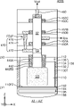
도 1은 예시적인 실시예들에 따른 이미지 센서(100)를 나타내는 레이아웃도이다. 도 2는 도 1의 II 부분의 확대 레이아웃이다. 도 3은 도 2의 A1-A1' 선 및 A2-A2' 선을 따른 단면도이다. 도 4는 도 3의 CX2 부분의 확대도이다. 도 5a 및 도 5b는 예시적인 실시예들에 따른 제1 게이트 전극(150)의 레이아웃도이다. 도 1 및 도 2에는 편의상 이미지 센서(100)의 일부 구성만이 도시된다. 1 is a layout diagram illustrating an
도 1 내지 도 5b를 참조하면, 이미지 센서(100)는 반도체 기판(110)에 형성된 액티브 픽셀 영역(APR), 주변 회로 영역(PCR), 및 패드 영역(PDR)을 포함할 수 있다.1 to 5B , the
액티브 픽셀 영역(APR)은 반도체 기판(110)의 중앙부에 배치될 수 있고, 액티브 픽셀 영역(APR)의 양 측 상에는 주변 회로 영역(PCR)이 배치될 수 있다. 반도체 기판(110)의 에지부에는 패드 영역(PDR)이 배치될 수 있다.The active pixel region APR may be disposed in a central portion of the
액티브 픽셀 영역(APR)은 복수의 픽셀(PX)을 포함하며, 복수의 픽셀(PX) 내에 각각 복수의 광전 변환 영역(120)이 배치될 수 있다. 액티브 픽셀 영역(APR)에서, 복수의 픽셀(PX)이 반도체 기판(110)의 상면에 평행한 제1 방향(X)과, 상기 제1 방향에 수직하여 반도체 기판(110)의 상면에 평행한 제2 방향(Y)을 따라 열과 행을 이루며 매트릭스 형상으로 배열될 수 있다. The active pixel region APR includes a plurality of pixels PX, and a plurality of
주변 회로 영역(PCR)은 평면적으로 액티브 픽셀 영역(APR)의 양 측 상에 배치된 것으로 예시적으로 도시되었지만, 이에 한정되는 것은 아니고 액티브 픽셀 영역(APR)의 전체를 둘러싸도록 배치될 수도 있다. 또는 도 19에 도시된 것과 같이 주변 회로 영역(PCR)은 다른 기판에 형성되어 액티브 픽셀 영역(APR)이 형성된 기판에 스택 형태로 연결될 수도 있다. 패드 영역(PDR)에는 도전 패드(PAD)가 배치될 수 있다. 도전 패드(PAD)는 반도체 기판(110)의 에지부 상에 배치될 수 있다.Although the peripheral circuit region PCR is exemplarily illustrated as being disposed on both sides of the active pixel region APR in a plan view, the present invention is not limited thereto, and the peripheral circuit region PCR may be disposed to surround the entire active pixel region APR. Alternatively, as shown in FIG. 19 , the peripheral circuit region PCR may be formed on another substrate and connected to the substrate on which the active pixel region APR is formed in a stack form. A conductive pad PAD may be disposed in the pad region PDR. The conductive pad PAD may be disposed on the edge portion of the
반도체 기판(110)은 서로 반대되는 제1 면(110F1) 및 제2 면(110F2)을 포함할 수 있다. 여기서는, 편의상 상부에 컬러 필터(186)가 배치되는 반도체 기판(110)의 표면을 제2 면(110F2)으로, 제2 면(110F2)에 반대되는 면을 제1 면(110F1)으로 지칭하였다. 그러나, 본 발명의 기술적 사상이 이에 한정되는 것은 아니다. The
예시적인 실시예들에 있어서, 반도체 기판(110)은 p형 반도체 기판을 포함할 수 있다. 예를 들면, 반도체 기판(110)은 Si, Ge, SiGe, SiC, GaAs, InAs, 및 InP 중 어느 하나를 포함할 수 있다. 예를 들어, 반도체 기판(110)은 p형 실리콘 기판으로 이루어질 수 있다. 예시적인 실시예들에서, 반도체 기판(110)은 p형 벌크 기판과 그 위에 성장된 p형 또는 n형 에피택셜층을 포함할 수 있다. 다른 실시예들에서, 반도체 기판(110)은 n형 벌크 기판과, 그 위에 성장된 p 형 또는 n형 에피택셜층을 포함할 수 있다. 또는, 반도체 기판(110)은 유기(organic) 플라스틱 기판으로 이루어질 수 있다. 반도체 기판(110)의 제1 면(110F1)에 인접한 반도체 기판(110)의 내부에는 웰 영역(114)이 배치될 수 있다. 웰 영역(114)은 p형 불순물이 도핑된 영역일 수 있다. In example embodiments, the
액티브 픽셀 영역(APR)에서 반도체 기판(110) 내에 복수의 픽셀(PX)이 매트릭스 형태로 배열될 수 있다. 복수의 픽셀(PX) 내에는 각각 복수의 광전 변환 영역(120)이 배치될 수 있다. 복수의 광전 변환 영역(120)은 반도체 기판(110)의 제2 면(110F2)으로부터 입사된 광이 전기적 신호로 변환되는 영역일 수 있다. A plurality of pixels PX may be arranged in a matrix in the
액티브 픽셀 영역(APR)에서 반도체 기판(110) 내에 픽셀 소자 분리막(130)이 배치되고, 픽셀 소자 분리막(130)에 의해 복수의 픽셀(PX)이 정의될 수 있다. 픽셀 소자 분리막(130)은 복수의 광전 변환 영역(120) 중 하나와 이에 인접한 광전 변환 영역(120) 사이에 배치될 수 있다. 하나의 광전 변환 영역(120)과 이와 이웃하는 다른 하나의 광전 변환 영역(120)은, 픽셀 소자 분리막(130)에 의해 물리적으로, 그리고 전기적으로 분리될 수 있다. 픽셀 소자 분리막(130)은 매트릭스 형태로 배열된 복수의 광전 변환 영역(120) 각각 사이에 배치되며, 평면도에서 그리드 또는 메쉬 형상을 가질 수 있다. A pixel
픽셀 소자 분리막(130)은 반도체 기판(110)의 제1 면(110F1)으로부터 제2 면(110F2)까지 반도체 기판(110)을 관통하는 픽셀 트렌치(130T) 내부에 형성될 수 있다. 픽셀 소자 분리막(130)은 픽셀 트렌치(130T) 측벽 상에 콘포말하게 형성되는 절연층(132)과, 절연층(132) 상에서 픽셀 트렌치(130T) 내부를 채우는 도전층(134)과, 상부 절연층(136)을 포함할 수 있다. 상부 절연층(136)은 반도체 기판(110)의 제1 면(110F1)에 인접한 픽셀 트렌치(130T)의 일부분 내에 상부 절연층(136)이 배치될 수 있다. 예시적인 실시예들에서, 상부 절연층(136)은 픽셀 트렌치(130T)의 입구에 배치되는 절연층(132) 및 도전층(134) 일부분을 에치백하고 남은 공간을 절연 물질로 채움에 의해 형성될 수 있다. The pixel
예시적인 실시예들에서, 절연층(132)은 하프늄 산화물, 알루미늄 산화물, 탄탈륨 산화물 등과 같은 금속 산화물을 포함할 수 있다. 이러한 경우에, 절연층(132)은 음의 고정 전하층(negative fixed charge layer)으로 작용할 수 있으나, 본 발명의 기술적 사상이 이에 한정되는 것은 아니다. 다른 실시예들에서, 절연층(132)은 실리콘 산화물, 실리콘 질화물, 실리콘 산질화물 등의 절연 물질을 포함할 수 있다. 도전층(134)은 도핑된 폴리실리콘, 금속, 금속 실리사이드, 금속 질화물, 또는 금속 함유막 중 적어도 하나를 포함할 수 있다.In example embodiments, the insulating
도 3에서는 픽셀 소자 분리막(130)이 반도체 기판(110)의 제1 면(110F1)으로부터 제2 면(110F2)까지 반도체 기판(110)을 관통하여 연장되는 것을 예시적으로 도시하였으나, 다른 실시예들에서, 도 3에 도시된 것과 달리 픽셀 소자 분리막(130)은 반도체 기판(110)의 제2 면(110F2)으로부터 반도체 기판(110)의 내부를 향해 연장되고 반도체 기판(110)의 제1 면(110F1)에 노출되지 않을 수 있다. 이러한 경우에, 반도체 기판(110)의 제1 면(110F1)과 인접한 픽셀 소자 분리막(130)의 일단과 제1 면(110F1) 사이에는 배리어 도핑 영역(도시 생략)이 형성될 수 있고, 상기 배리어 도핑 영역은 p형 불순물이 고농도로 도핑된 영역일 수 있다. In FIG. 3 , the pixel
도 3에 예시적으로 도시된 바와 같이, 반도체 기판(110)의 제1 면(110F1) 상에는 활성 영역(도시 생략)을 정의하는 소자 분리막(112)이 형성될 수 있다. 소자 분리막(112)은 반도체 기판(110)의 제1 면(110F1)에 소정의 깊이로 형성된 소자 분리 트렌치(도시 생략) 내에 배치되고, 절연 물질을 포함할 수 있다. 소자 분리막(112)은 픽셀 소자 분리막(130)의 상부 측벽(예를 들어, 상부 절연층(136)의 측벽)을 둘러싸도록 배치될 수 있다. 3 , a
상기 활성 영역 상에는 픽셀 회로(도시 생략)를 구성하는 트랜지스터들이 배치될 수 있다. 상기 활성 영역은 그 상부에 전송 게이트(TG), 소스 팔로워 게이트(SF), 선택 게이트(SEL), 리셋 게이트(RG)가 배치되는 반도체 기판(110)의 일부분일 수 있다. 예를 들어, 상기 활성 영역은 그라운드 영역(GND), 플로팅 확산(floating diffusion) 영역(FD) 및 제1 소스/드레인 영역(SD1)을 포함할 수 있다. 그라운드 영역(GND), 플로팅 확산 영역(FD) 및 제1 소스/드레인 영역(SD1)은 소자 분리막(112)에 의해 서로 이격되어 배치될 수 있다. Transistors constituting a pixel circuit (not shown) may be disposed on the active region. The active region may be a portion of the
일부 예시적인 실시예들에서, 도 2에 도시된 것과 같이, 제1 픽셀(PX-1), 제2 픽셀(PX-2), 제3 픽셀(PX-3), 및 제4 픽셀(PX-4)이 매트릭스 형상으로 배치될 수 있고, 제2 방향(Y)으로 나란히 배치되는 제1 픽셀(PX-1)과 제3 픽셀(PX-3)은 서로 거울 대칭 형상을 가질 수 있고, 제1 방향(X)으로 나란히 배치되는 제1 픽셀(PX-1)과 제2 픽셀(PX-2)은 서로 거울 대칭 형상을 가질 수 있다. In some example embodiments, as shown in FIG. 2 , the first pixel PX-1, the second pixel PX-2, the third pixel PX-3, and the fourth pixel PX- 4) may be disposed in a matrix shape, and the first pixel PX-1 and the third pixel PX-3 disposed side by side in the second direction Y may have a mirror-symmetric shape with each other. The first pixel PX-1 and the second pixel PX-2 arranged side by side in the direction X may have a mirror-symmetrical shape.
일부 예시적인 실시예들에서, 제1 픽셀(PX-1) 및 제2 픽셀(PX-2)은 전송 게이트(TG) 및 소스 팔로워 게이트(SF)를 포함할 수 있고, 제3 픽셀(PX-3)은 전송 게이트(TG) 및 리셋 게이트(RG)를 포함할 수 있고, 제4 픽셀(PX-4)은 전송 게이트(TG) 및 선택 게이트(SEL)를 포함할 수 있다. 그러나 도 2에 도시된 것은 일부 실시예들에 따른 트랜지스터들의 레이아웃에 해당하며, 트랜지스터들의 레이아웃 또는 활성 영역(ACT)의 형상이 이에 한정되는 것은 아니다. In some example embodiments, the first pixel PX-1 and the second pixel PX-2 may include a transfer gate TG and a source follower gate SF, and the third pixel PX- 3) may include a transfer gate TG and a reset gate RG, and the fourth pixel PX-4 may include a transfer gate TG and a selection gate SEL. However, the layout of the transistors illustrated in FIG. 2 corresponds to the layout of the transistors according to some embodiments, and the layout of the transistors or the shape of the active region ACT is not limited thereto.
예시적인 실시예들에서, 전송 게이트(TG)는 전송 트랜지스터(TX)(도 6 참조)를 구성할 수 있고, 전송 트랜지스터(TX)는 광전 변환 영역(120)에서 생성된 전하를 플로팅 확산 영역(FD)에 전송하도록 구성될 수 있다. 리셋 게이트(RG)는 리셋 트랜지스터(RX)(도 6 참조)를 구성할 수 있고, 리셋 트랜지스터(RX)는 플로팅 확산 영역(FD)에 저장되어 있는 전하를 주기적으로 리셋시키도록 구성될 수 있다. 소스 팔로워 게이트(SF)는 드라이브 트랜지스터(DX)(도 6 참조)를 구성할 수 있고, 드라이브 트랜지스터(DX)는 소스 팔로워 버퍼 증폭기(source follower buffer amplifier) 역할을 하며 상기 플로팅 확산 영역에 충전된 전하에 따른 신호를 버퍼링하도록 구성될 수 있다. 선택 게이트(SEL)는 선택 트랜지스터(SX)(도 6 참조)를 구성할 수 있고, 선택 트랜지스터(SX)는 픽셀(PX)을 선택하기 위한 스위칭 및 어드레싱 역할을 할 수 있다. In exemplary embodiments, the transfer gate TG may constitute a transfer transistor TX (see FIG. 6 ), and the transfer transistor TX transfers charges generated in the
도 3에 예시적으로 도시된 것과 같이, 전송 게이트(TG)는 매립 전송 게이트 전극(140)으로 지칭될 수 있고, 매립 전송 게이트 전극(140)은 반도체 기판(110)의 제1 면(110F1)으로부터 반도체 기판(110) 내부로 연장되는 전송 게이트 트렌치(140T) 내부에 배치될 수 있다. 전송 게이트 트렌치(140T) 내벽 상에는 전송 게이트 절연층(142)이 콘포말하게 배치될 수 있고, 매립 전송 게이트 전극(140)은 전송 게이트 절연층(142) 상에서 전송 게이트 트렌치(140T) 내부를 채울 수 있다. As exemplarily illustrated in FIG. 3 , the transfer gate TG may be referred to as a buried
예를 들어, 매립 전송 게이트 전극(140)의 상면은 반도체 기판(110)의 제1 면(110F1)보다 높은 레벨에 배치될 수 있고, 매립 전송 게이트 전극(140)의 측벽 상에는 전송 게이트 스페이서(144)가 배치될 수 있다. For example, the top surface of the buried
예시적인 실시예들에서, 매립 전송 게이트 전극(140)은 도핑된 폴리실리콘, 금속, 금속 실리사이드, 금속 질화물, 또는 금속 함유막 중 적어도 하나를 포함할 수 있다. 전송 게이트 절연층(142)은 실리콘 산화물, 또는 금속 산화물을 포함할 수 있고, 전송 게이트 스페이서(144)는 실리콘 질화물, 실리콘 산질화물, 또는 실리콘 산화물을 포함할 수 있다. In example embodiments, the buried
리셋 게이트(RG), 소스 팔로워 게이트(SF) 및 선택 게이트(SEL)는 제1 게이트 전극(150)으로 지칭될 수 있고, 제1 게이트 전극(150)은 반도체 기판(110)의 제1 면(110F1) 상에 배치되는 반도체 패턴(AP)의 측벽(APS)을 둘러싸도록 배치될 수 있다. 반도체 패턴(AP)과 이를 둘러싸는 제1 게이트 전극(150)은 게이트-올-어라운드(gate-all-around) 타입의 트랜지스터를 구성할 수 있다.The reset gate RG, the source follower gate SF, and the selection gate SEL may be referred to as a
반도체 패턴(AP)은 반도체 기판(110)의 제1 면(110F1)으로부터 수직 방향(Z)을 따라 연장될 수 있다. 예를 들어, 반도체 패턴(AP)은 Si, Ge, SiGe, SiC, GaAs, InAs, 및 InP 중 어느 하나를 포함할 수 있다. The semiconductor pattern AP may extend along the vertical direction Z from the first surface 110F1 of the
예시적인 실시예들에서, 반도체 패턴(AP)은 반도체 기판(110)의 제1 면(110F1)을 시드층으로 하여 에피택셜 성장된 물질층을 포함할 수 있다. 다른 실시예들에서, 반도체 패턴(AP)은 반도체 기판(110)의 일부분이고, 반도체 기판(110)의 제1 면(110F1) 상에 마스크 패턴(도시 생략)을 형성한 후 반도체 기판(110)을 소정의 두께만큼 식각함에 의해 형성될 수 있고, 반도체 기판(110)의 제1 면으로부터 수직 방향(Z)으로 돌출하도록 잔류하는 반도체 기판(110)의 일부분일 수 있다. In example embodiments, the semiconductor pattern AP may include a material layer epitaxially grown using the first surface 110F1 of the
예를 들어, 반도체 기판(110)의 제2 면(110F2)이 제1 수직 레벨(LV1)에 배치되고, 반도체 기판(110)의 제1 면(110F1)이 제2 수직 레벨(LV2)에 배치된다. 제1 수직 레벨(LV1)을 기준으로 할 때, 반도체 패턴(AP)의 상면은 제2 수직 레벨(LV2)보다 더 높은 제3 수직 레벨(LV3)에 배치될 수 있다. 예를 들어, 반도체 패턴(AP)의 상면으로부터 반도체 기판(110)의 제2 면(110F2)까지의 거리가 반도체 기판(110)의 제1 면(110F1)으로부터 반도체 기판(110)의 제2 면(110F2)까지의 거리(즉, 반도체 기판(110)의 높이)보다 더 클 수 있다. For example, the second surface 110F2 of the
도 3에 도시된 것과 같이, 반도체 패턴(AP)은 수직 방향(Z)을 따라 제1 높이(h11)를 가질 수 있고, 제1 높이(h11)는 약 10 내지 500 nm의 범위일 수 있으나, 이에 한정되는 것은 아니다. As shown in FIG. 3 , the semiconductor pattern AP may have a first height h11 in the vertical direction Z, and the first height h11 may be in a range of about 10 to 500 nm, The present invention is not limited thereto.
도 3에서, 반도체 패턴(AP)은 반도체 기판(110)의 제1 면(110F1)에 수직한 측벽(APS)을 가지며 전체 높이(h11)에 걸쳐 제1 방향(X)에 따른 폭이 실질적으로 동일한 것으로 예시적으로 도시되었다. 그러나 반도체 패턴(AP)의 형성 공정에 따라 반도체 패턴(AP)의 측벽 기울기는 달라질 수 있다. 예를 들어, 반도체 기판(110)의 제1 면(110F1) 상에 개구부(도시 생략)를 갖는 몰드층(도시 생략)을 형성하고, 상기 몰드층 내에 에피택셜 공정에 의해 반도체 패턴(AP)을 형성할 수 있고, 이러한 경우에 반도체 패턴(AP)의 상면 폭이 반도체 패턴(AP)의 바닥면 폭보다 더 클 수도 있다. 이와는 반대로, 반도체 패턴(AP)의 제1 면(110F1)으로부터 소정의 두께를 식각하여 반도체 패턴(AP)을 형성하는 경우, 반도체 패턴(AP)의 상면 폭이 반도체 패턴(AP)의 바닥면 폭보다 더 작을 수도 있다.In FIG. 3 , the semiconductor pattern AP has a sidewall APS perpendicular to the first surface 110F1 of the
도 2에서, 반도체 패턴(AP)은 실질적으로 원형인 수평 단면을 가진 것으로 도시된다. 그러나 다른 실시예들에서, 도 5a에 도시된 것과 같이, 반도체 패턴(AP)은 타원형의 수평 단면을 가질 수 있고, 예를 들어, 제1 방향(X)에 따른 폭이 제2 방향(Y)에 따른 폭보다 더 클 수 있다(또는 이와는 반대로, 제1 방향(X)에 따른 폭이 제2 방향(Y)에 따른 폭보다 더 작을 수도 있다). 다른 실시예들에서, 도 5b에 도시된 것과 같이, 반도체 패턴(AP)은 직사각형의 수평 단면을 가질 수 있으나, 반도체 패턴(AP)의 수평 단면 형상이 이에 한정되는 것은 아니다.In FIG. 2 , the semiconductor pattern AP is illustrated as having a substantially circular horizontal cross-section. However, in other embodiments, as shown in FIG. 5A , the semiconductor pattern AP may have an elliptical horizontal cross-section, and for example, a width along the first direction X may increase in the second direction Y. (or conversely, the width along the first direction (X) may be smaller than the width along the second direction (Y)). In other embodiments, as illustrated in FIG. 5B , the semiconductor pattern AP may have a rectangular horizontal cross-section, but the horizontal cross-sectional shape of the semiconductor pattern AP is not limited thereto.
제1 게이트 전극(150)은 반도체 기판(110)의 제1 면(110F1) 상에서 반도체 패턴(AP)의 측벽(APS)을 둘러쌀 수 있다. 예를 들어, 제1 게이트 전극(150)은 반도체 패턴(AP)의 측벽(APS)을 둘러싸는 메인 전극부(MP)와, 메인 전극부(MP)로부터 수평 방향으로 연장되어 반도체 기판(110)의 제1 면(110F1) 상에 배치되는 연장부(EXP)를 포함할 수 있다. 예를 들어, 메인 전극부(MP)는 반도체 패턴(AP)의 측벽(APS) 상에서 반도체 패턴(AP)의 상면보다 낮은 제4 수직 레벨(LV4)까지 수직 방향(Z)으로 연장될 수 있다. 평면도에서 메인 전극부(MP)는 링 형상을 가질 수 있고, 메인 전극부(MP)의 측벽(APS) 전체를 포위할 수 있다. The
연장부(EXP)는 반도체 기판(110)의 제1 면(110F1) 상에서 평탄한 상면 레벨을 가지며 소정의 폭으로 형성될 수 있다. 연장부(EXP)의 상부에 콘택(162)(예를 들어, 제2 콘택(CA2))이 배치될 수 있고, 이에 따라 콘택(162)을 통해 제1 게이트 전극(150)에 전기적 신호가 인가될 수 있다. 제1 게이트 전극(150)이 메인 전극부(MP)로부터 연장되는 평탄한 상면을 갖는 연장부(EXP)를 포함함에 따라 제1 게이트 전극(150)에 대한 콘택(162)을 형성하기 위한 공정 불량이 방지될 수 있다. 예시적인 실시예들에서, 연장부(EXP)의 상면은 매립 전송 게이트 전극(140)의 상면과 동일한 레벨에 배치될 수 있으나, 이에 한정되는 것은 아니다.The extension EXP may be formed on the first surface 110F1 of the
제1 게이트 절연층(152)은 반도체 패턴(AP)과 제1 게이트 전극(150) 사이에 개재될 수 있고, 반도체 패턴(AP)의 측벽(APS)을 둘러쌀 수 있다. 제1 게이트 절연층(152)은 반도체 패턴(AP)의 측벽(APS) 상으로부터 반도체 기판(110)의 제1 면(110F1) 상으로 연장될 수 있으나, 이에 한정되는 것은 아니다. 제1 게이트 절연층(152)은 전송 게이트 트렌치(140T) 내부까지 연장되어 전송 게이트 절연층(142)과 연결되는 연속적인 물질층으로 형성될 수도 있다. 이와는 달리 제1 게이트 절연층(152)은 반도체 기판(110)의 제1 면(110F1) 상으로 연장되되 전송 게이트 트렌치(140T) 내부까지 연장되지 않을 수 있고, 전송 게이트 절연층(142)과는 별개의 물질층으로 형성될 수도 있다.The first
반도체 패턴(AP)은 제1 소스/드레인 영역(SD1) 상에 배치될 수 있고, 반도체 패턴(AP)의 상측은 메인 전극부(MP)에 의해 커버되지 않을 수 있고, 반도체 패턴(AP)의 상측에 제2 소스/드레인 영역(SD2)이 배치될 수 있다. 제1 소스/드레인 영역(SD1) 및 제2 소스/드레인 영역(SD2)은 불순물이 고농도로 도핑된 영역일 수 있다. 예를 들어, 반도체 패턴(AP)과, 제1 게이트 전극(150)의 메인 전극부(MP), 제1 소스/드레인 영역(SD1) 및 제2 소스/드레인 영역(SD2)은 게이트-올-어라운드 타입 트랜지스터를 구성할 수 있다. The semiconductor pattern AP may be disposed on the first source/drain region SD1 , and an upper side of the semiconductor pattern AP may not be covered by the main electrode part MP, and A second source/drain region SD2 may be disposed on the upper side. The first source/drain region SD1 and the second source/drain region SD2 may be regions doped with a high concentration of impurities. For example, the semiconductor pattern AP, the main electrode part MP of the
예시적인 실시예들에서, 제1 게이트 전극(150)은 도핑된 폴리실리콘, 금속, 금속 실리사이드, 금속 질화물, 또는 금속 함유막 중 적어도 하나를 포함할 수 있다. 제1 게이트 절연층(152)은 실리콘 산화물, 또는 금속 산화물을 포함할 수 있으나, 이에 한정되는 것은 아니다.In example embodiments, the
반도체 기판(110)의 제1 면(110F1) 상에는 매립 절연층(160)이 배치될 수 있다. 매립 절연층(160)은 그라운드 영역(GND), 플로팅 확산 영역(FD), 소자 분리막(112), 매립 전송 게이트 전극(140), 반도체 패턴(AP), 및 제1 게이트 전극(150)을 커버할 수 있다. 매립 절연층(160)은 반도체 패턴(AP) 및 제1 게이트 전극(150)의 상면을 덮기에 충분한 높이로 형성될 수 있다. A buried insulating
예시적인 실시예들에서, 매립 절연층(160)은 실리콘 질화물, 실리콘 산질화물을 포함할 수 있다. 일부 예시들에서, 매립 절연층(160)은 제1 절연층(도시 생략)과 제2 절연층(도시 생략)의 적층 구조로 형성될 수 있다. 다른 예시들에서, 매립 절연층(160)과 반도체 기판(110)의 제1 면(110F1) 사이에 식각 정지층(도시 생략)이 개재될 수도 있고, 상기 식각 정지층은 매립 절연층(160)에 대하여 식각 선택비를 갖는 물질을 포함할 수 있다.In example embodiments, the buried insulating
반도체 기판(110)의 제1 면(110F1) 상에는 매립 절연층(160)을 관통하는 콘택(162)이 배치될 수 있다. 예를 들어, 콘택(162)은 매립 절연층(160)을 관통하여 활성 영역(도시 생략), 매립 전송 게이트 전극(140), 및 제1 게이트 전극(150)에 전기적으로 연결될 수 있다. 콘택(162)은 제1 콘택(CA1), 제2 콘택(CA2), 및 제3 콘택(CA3)을 포함할 수 있다. A
제1 콘택(CA1)은 매립 절연층(160)을 관통하는 제1 콘택홀(CA1H) 내에 배치될 수 있다. 제1 콘택홀(CA1H)은 반도체 기판(110)의 제1 면(110F1)의 상면을 노출할 수 있고, 예를 들어 그라운드 영역(GND) 및 플로팅 확산 영역(FD)을 노출할 수 있다. 제1 콘택(CA1)은 제1 콘택홀(CA1H) 내부를 채우며 그라운드 영역(GND) 및 플로팅 확산 영역(FD)과 연결될 수 있다.The first contact CA1 may be disposed in the first contact hole CA1H passing through the buried insulating
제2 콘택(CA2)은 매립 절연층(160)을 관통하는 제2 콘택홀(CA2H) 내에 배치될 수 있다. 제2 콘택홀(CA2H)은 매립 전송 게이트 전극(140)의 상면 및 제1 게이트 전극(150)의 상면을 노출할 수 있다. 예를 들어, 제2 콘택홀(CA2H)은 제1 게이트 전극(150)의 연장부(EXP)의 상면을 노출할 수 있다. 제2 콘택(CA2)은 제2 콘택홀(CA2H) 내부를 채우며 매립 전송 게이트 전극(140)의 상면 및 제1 게이트 전극(150)의 연장부(EXP)의 상면과 연결될 수 있다. The second contact CA2 may be disposed in the second contact hole CA2H passing through the buried insulating
제3 콘택(CA3)은 매립 절연층(160)을 관통하는 제3 콘택홀(CA3H) 내에 배치될 수 있다. 제3 콘택홀(CA3H)은 반도체 패턴(AP)의 상면, 또는 제2 소스/드레인 영역(SD2)의 상면을 노출할 수 있다. 제3 콘택(CA3)은 제3 콘택홀(CA3H) 내부를 채우며 제2 소스/드레인 영역(SD2)과 연결될 수 있다. The third contact CA3 may be disposed in the third contact hole CA3H passing through the buried insulating
매립 절연층(160) 상에는 상부 배선 구조물(170)이 배치될 수 있다. 상부 배선 구조물(170)은 복수의 층들의 적층 구조로 형성될 수 있다. 상부 배선 구조물(170)은 배선층(172) 및 배선층(172)을 둘러싸는 절연층(174)을 포함할 수 있다. 배선층(172)은 불순물이 도핑되거나 도핑되지 않은 폴리실리콘, 금속, 금속 실리사이드, 금속 질화물, 또는 금속 함유막 중 적어도 하나를 포함할 수 있다. 예를 들어, 배선층(172)은 텅스텐, 알루미늄, 구리, 텅스텐 실리사이드, 티타늄 실리사이드, 텅스텐 질화물, 티타늄 질화물, 도핑된 폴리실리콘 등을 포함할 수 있다. 절연층(174)은 실리콘 산화물, 실리콘 질화물, 실리콘 산질화물 등의 절연 물질을 포함할 수 있다.An
반도체 기판(110)의 제2 면(110F2) 상에는 후면 절연층(182)이 배치될 수 있다. 후면 절연층(182)은 반도체 기판(110)의 제2 면(110F2)의 실질적으로 전체 면적 상에 배치될 수 있고, 후면 절연층(182)이 반도체 기판(110)의 제2 면(110F2)과 동일 레벨에 배치되는 픽셀 소자 분리막(130)의 상면과 접촉할 수 있다. 예시적인 실시예들에서, 후면 절연층(182)은 하프늄 산화물, 알루미늄 산화물, 탄탈륨 산화물 등과 같은 금속 산화물을 포함할 수 있다. 다른 실시예들에서, 후면 절연층(182)은 실리콘 산화물, 실리콘 질화물, 실리콘 산질화물, 저유전율 물질 등의 절연 물질을 포함할 수 있다.A rear insulating
후면 절연층(182) 상에 패시베이션층(184)이 배치될 수 있고, 패시베이션층(184) 상에는 컬러 필터(186)와 마이크로렌즈(188)가 배치될 수 있다. 선택적으로, 반도체 기판(110)의 제1 면(110F1) 상에는 지지 기판(도시 생략)이 더 배치될 수 있다.A
일반적으로 픽셀(PX)에 배치되는 리셋 게이트(RG), 선택 게이트(SEL), 및 소스 팔로워 게이트(SF)와 같은 픽셀 회로들은 픽셀 내에서 수평 방향으로 서로 이격되어 배치된다. 이미지 센서의 집적도가 증가함에 따라 단위 픽셀의 크기가 작아지고 픽셀 회로의 각각의 구성요소들의 크기 또한 작아지므로, 픽셀 회로를 통한 누설 전류 또는 픽셀 회로의 리드 노이즈(read noise) 등이 발생하여 이미지 센서의 품질이 저하되는 문제가 있다. In general, pixel circuits such as a reset gate RG, a selection gate SEL, and a source follower gate SF disposed in the pixel PX are horizontally spaced apart from each other in the pixel. As the degree of integration of the image sensor increases, the size of the unit pixel decreases and the size of each component of the pixel circuit also decreases, so that leakage current through the pixel circuit or read noise of the pixel circuit occurs, and thus the image sensor There is a problem that the quality of
그러나 예시적인 실시예들에 따르면, 반도체 패턴(AP)이 수직 방향(Z)으로 연장되고, 제1 게이트 전극(150)이 반도체 패턴(AP)의 측벽을 둘러싸는 게이트-올-어라운드 구조를 가질 수 있다. 이에 따라 리셋 게이트(RG), 선택 게이트(SEL), 및 소스 팔로워 게이트(SF)와 같은 픽셀 회로들의 누설 전류가 감소하고 리드 노이즈 발생이 방지될 수 있다. 따라서 이미지 센서(100)는 우수한 이미지 품질을 가질 수 있다. 또한 반도체 패턴(AP)과 제1 게이트 전극(150)이 수직 방향(Z)으로 연장됨에 따라 단위 픽셀의 면적이 감소될 수 있고, 이미지 센서(100)의 소형화가 구현될 수 있다. However, according to example embodiments, the semiconductor pattern AP may extend in the vertical direction Z and the
도 6은 예시적인 실시예들에 따른 이미지 센서(100)의 픽셀(PX)의 등가 회로도이다. 6 is an equivalent circuit diagram of a pixel PX of the
도 6을 참조하면, 복수의 픽셀(PX)는 매트릭스 형태로 배열될 수 있다. 복수의 픽셀(PX) 각각은 전송 트랜지스터(TX)와 로직 트랜지스터들을 포함할 수 있다. 여기서, 로직 트랜지스터들은 리셋 트랜지스터(RX), 선택 트랜지스터(SX), 및 드라이브 트랜지스터(DX)(또는 소스 팔로워 트랜지스터)를 포함할 수 있다. 리셋 트랜지스터(RX)는 리셋 게이트(RG)를 포함하고, 선택 트랜지스터(SX)는 선택 게이트(SEL)를 포함하며, 드라이브 트랜지스터(DX)는 소스 팔로워 게이트(SF)를 포함하고, 전송 트랜지스터(TX)는 전송 게이트(TG)를 포함할 수 있다. Referring to FIG. 6 , the plurality of pixels PX may be arranged in a matrix form. Each of the plurality of pixels PX may include a transfer transistor TX and logic transistors. Here, the logic transistors may include a reset transistor RX, a selection transistor SX, and a drive transistor DX (or a source follower transistor). The reset transistor RX includes a reset gate RG, the selection transistor SX includes a selection gate SEL, the drive transistor DX includes a source follower gate SF, and the transfer transistor TX ) may include a transfer gate TG.
복수의 픽셀(PX) 각각은 광전 변환 소자(PD) 및 플로팅 확산 영역(FD)을 더 포함할 수 있다. 광전 변환 소자(PD)는 도 1 내지 도 4에서 설명한 광전 변환 영역(120)에 대응될 수 있다. 광전 변환 소자(PD)는 외부에서 입사된 빛의 양에 비례하여 광전하들을 생성 및 축적할 수 있고, 포토 다이오드, 포토 트랜지스터(photo transistor), 포토 게이트, 핀드 포토 다이오드(Pinned Photo Diode; PPD) 및 이들의 조합이 사용될 수 있다. Each of the plurality of pixels PX may further include a photoelectric conversion element PD and a floating diffusion region FD. The photoelectric conversion device PD may correspond to the
전송 게이트(TG)는 상기 광전 변환 소자에서 생성된 전하를 플로팅 확산 영역(FD)으로 전송할 수 있다. 플로팅 확산 영역(FD)은 광전 변환 소자(PD)에서 생성된 전하를 전송받아 누적으로 저장할 수 있다. 플로팅 확산 영역(FD)에 축적된 광전하들의 양에 따라 드라이브 트랜지스터(DX)가 제어될 수 있다.The transfer gate TG may transfer charges generated by the photoelectric conversion element to the floating diffusion region FD. The floating diffusion region FD may receive and accumulate charges generated by the photoelectric conversion device PD. The drive transistor DX may be controlled according to the amount of photocharges accumulated in the floating diffusion region FD.
리셋 트랜지스터(RX)는 플로팅 확산 영역(FD)에 축적된 전하들을 주기적으로 리셋시킬 수 있다. 리셋 트랜지스터(RX)의 드레인 전극은 플로팅 확산 영역(FD)와 연결되며 소스 전극은 전원 전압(VDD1)에 연결된다. 리셋 트랜지스터(RX)가 턴-온(turn-on)되면, 리셋 트랜지스터(RX)의 소스 전극과 연결된 전원 전압(VDD1)이 상기 플로팅 확산 영역(FD)로 전달된다. 리셋 트랜지스터(RX)가 턴-온될 때 플로팅 확산 영역(FD)에 축적된 전하들이 배출되어 플로팅 확산 영역(FD)이 리셋될 수 있다.The reset transistor RX may periodically reset charges accumulated in the floating diffusion region FD. The drain electrode of the reset transistor RX is connected to the floating diffusion region FD, and the source electrode is connected to the power supply voltage V DD1 . When the reset transistor RX is turned on, the power voltage V DD1 connected to the source electrode of the reset transistor RX is transferred to the floating diffusion region FD. When the reset transistor RX is turned on, charges accumulated in the floating diffusion region FD may be discharged to reset the floating diffusion region FD.
드라이브 트랜지스터(DX)는 복수의 픽셀(PX) 외부에 위치하는 전류원(도시 생략)과 연결되어 소스 팔로워 버퍼 증폭기(source follower buffer amplifier)로 기능하고, 플로팅 확산 영역(FD)에서의 전위 변화를 증폭하고 이를 출력 라인(VOUT)으로 출력한다.The drive transistor DX is connected to a current source (not shown) positioned outside the plurality of pixels PX to function as a source follower buffer amplifier, and amplifies a change in potential in the floating diffusion region FD. and output it to the output line (V OUT ).
선택 트랜지스터(SX)는 행 단위로 복수의 픽셀(PX)를 선택할 수 있고, 선택 트랜지스터(SX)가 턴-온될 때 전원 전압(VDD2)이 드라이브 트랜지스터(DX)의 소스 전극으로 전달될 수 있다.The selection transistor SX may select the plurality of pixels PX in a row unit, and when the selection transistor SX is turned on, the power voltage V DD2 may be transferred to the source electrode of the drive transistor DX. .
도 7은 예시적인 실시예들에 따른 이미지 센서(100A)를 나타내는 레이아웃도이다. 도 7에서, 도 1 내지 도 6에서와 동일한 참조부호는 동일한 구성요소를 의미한다.7 is a layout diagram illustrating an
도 7을 참조하면, 이미지 센서(100A)는 듀얼 게이트 구조를 갖는 전송 게이트(TG)를 포함할 수 있다. 도 7에서는 매립 전송 게이트 전극(140)(도 2 참조) 대신 한 쌍의 매립 전송 게이트 전극(140A)을 포함할 수 있고, 한 쌍의 매립 전송 게이트 전극(140A)은 서로 소정의 거리로 이격되어 플로팅 확산 영역(FD)에 인접하게 배치될 수 있다. Referring to FIG. 7 , the
도 8은 예시적인 실시예들에 따른 이미지 센서(100B)를 나타내는 레이아웃도이고, 도 9는 도 8의 A1-A1' 선 및 A2-A2' 선을 따른 단면도이다. 도 8 및 도 9에서, 도 1 내지 도 7에서와 동일한 참조부호는 동일한 구성요소를 의미한다.8 is a layout diagram illustrating an
도 8을 참조하면, 이미지 센서(100B)는 링 형상의 게이트 구조를 갖는 전송 게이트(TG)를 포함할 수 있다. 전송 게이트 트렌치(140TB)는 플로팅 확산 영역(FD)을 둘러싸도록 배치되고, 평면도에서 링 형상을 가질 수 있다. 매립 전송 게이트 전극(140B)은 전송 게이트 트렌치(140TB) 내에 배치되고 플로팅 확산 영역(FD)을 둘러싸도록 배치될 수 있다. Referring to FIG. 8 , the
예시적인 실시예들에서, 매립 전송 게이트 전극(140B)은 메인 전극부(140MP)와 연장부(140EX)를 포함할 수 있고, 메인 전극부(140MP)는 전송 게이트 트렌치(140TB) 내에 배치되며 평면도에서 링 형상을 가질 수 있다. 연장부(140EX)는 메인 전극부(140MP)로부터 반도체 기판(110)의 제1 면(110F1) 상으로 연장될 수 있다. 연장부(140EX) 상에 콘택(162)(예를 들어, 제2 콘택(CA2))이 배치될 수 있고, 콘택(162)을 통해 매립 전송 게이트 전극(140B)에 전기적 신호가 인가될 수 있다.In example embodiments, the buried
매립 전송 게이트 전극(140B)이 메인 전극부(140MP)로부터 연장되는 평탄한 상면을 갖는 연장부(140EX)를 포함함에 따라 매립 전송 게이트 전극(140B)에 대한 콘택(162)을 형성하기 위한 공정에서의 불량이 방지될 수 있다. 예시적인 실시예들에서, 연장부(140EX)의 상면은 제1 게이트 전극(150)의 연장부(EXP)의 상면과 동일한 레벨에 배치될 수 있으나, 이에 한정되는 것은 아니다.In the process for forming the
예시적인 실시예들에 따르면, 매립 전송 게이트 전극(140B)이 플로팅 확산 영역(FD)을 둘러싸도록 배치됨에 따라 전하 이동 경로가 반도체 기판(110)의 제1 면(110F1)에 수직한 방향을 따라 형성될 수 있다. 따라서 매립 전송 게이트 전극(140B)의 형상에 따라 쉽게 열화될 수 있는 저조도 특성 민감도가 개선될 수 있고, 이미지 센서(100B)는 우수한 품질을 가질 수 있다.According to example embodiments, as the buried
도 10은 예시적인 실시예들에 따른 이미지 센서(100C)를 나타내는 레이아웃도이다. 도 10에서, 도 1 내지 도 9에서와 동일한 참조부호는 동일한 구성요소를 의미한다.10 is a layout diagram illustrating an
도 10을 참조하면, 이미지 센서(100C)는 각각의 픽셀(PX-1, PX-2, PX-3, PX-4) 내에 서로 이격된 2개의 반도체 패턴(AP)을 포함할 수 있고, 각각의 반도체 패턴(AP)의 측벽 상에 제1 게이트 전극(150C1)과 제2 게이트 전극(150C2)이 배치될 수 있다. 예를 들어, 제1 게이트 전극(150C1)과 제2 게이트 전극(150C2) 각각은 메인 전극부(MP)와 연장부(EXP)를 포함할 수 있다. Referring to FIG. 10 , the
일부 예시들에서, 제1 게이트 전극(150C1)은 소스 팔로워 게이트(SF)(도 6 참조)일 수 있고, 제2 게이트 전극(150C2)은 선택 게이트(SEL)(도 6 참조)일 수 있다. 다른 예시들에서, 제1 게이트 전극(150C1)은 리셋 게이트(RG)(도 6 참조)일 수 있고, 제2 게이트 전극(150C2)은 선택 게이트(SEL)일 수 있다. 또 다른 예시들에서, 제1 게이트 전극(150C1)은 리셋 게이트(RG)일 수 있고, 제2 게이트 전극(150C2)은 소스 팔로워 게이트(SF)일 수 있다.In some examples, the first gate electrode 150C1 may be a source follower gate SF (see FIG. 6 ), and the second gate electrode 150C2 may be a selection gate SEL (see FIG. 6 ). In other examples, the first gate electrode 150C1 may be a reset gate RG (refer to FIG. 6 ), and the second gate electrode 150C2 may be a selection gate SEL. In still other examples, the first gate electrode 150C1 may be a reset gate RG, and the second gate electrode 150C2 may be a source follower gate SF.
도 10에는 제1 내지 제4 픽셀(PX-1, PX-2, PX-3, PX-4) 모두가 제1 게이트 전극(150C1)과 제2 게이트 전극(150C2)를 포함하는 것이 예시적으로 도시되었으나, 이와는 달리 제1 내지 제4 픽셀(PX-1, PX-2, PX-3, PX-4) 중 적어도 하나에서 제1 게이트 전극(150C1)과 제2 게이트 전극(150C2) 중 어느 하나가 생략될 수도 있다.10 , it is exemplarily illustrated that all of the first to fourth pixels PX-1, PX-2, PX-3, and PX-4 include a first gate electrode 150C1 and a second gate electrode 150C2. Although illustrated, unlike this, at least one of the first gate electrode 150C1 and the second gate electrode 150C2 in at least one of the first to fourth pixels PX-1, PX-2, PX-3, and PX-4. may be omitted.
도 11은 예시적인 실시예들에 따른 이미지 센서(200)를 나타내는 레이아웃도이다. 도 11에서, 도 1 내지 도 10에서와 동일한 참조부호는 동일한 구성요소를 의미한다.11 is a layout diagram illustrating an
도 11을 참조하면, 평면도에서 픽셀 소자 분리막(130A)은 픽셀(PX-1, PX-2, PX-3, PX-4) 각각을 완전히 둘러싸도록 배치되지 않을 수 있다. 픽셀 소자 분리막(130A)이 픽셀(PX-1, PX-2, PX-3, PX-4)을 둘러싸지 않는 반도체 기판(110)의 부분을 공유 영역(130XE)으로 지칭할 수 있다. 공유 영역(130XE) 내에는 그라운드 영역(GNDA)이 배치될 수 있고, 예를 들어, 그라운드 영역(GNDA)이 제1 픽셀(PX-1)과 제2 픽셀(PX-2)에 의해 공유되거나, 제3 픽셀(PX-3)과 제4 픽셀(PX-4)에 의해 공유될 수 있다.Referring to FIG. 11 , in a plan view, the
도 11에는 링 형상의 수평 단면을 갖는 매립 전송 게이트 전극(140B)이 도시되었으나, 매립 전송 게이트 전극(140B) 대신에 매립 전송 게이트 전극(140)(도 1 내지 도 4 참조), 또는 매립 전송 게이트 전극(140A)(도 7 참조)이 제공될 수도 있다.11 shows a buried
도 12는 예시적인 실시예들에 따른 이미지 센서(200A)를 나타내는 레이아웃도이다. 도 12에서, 도 1 내지 도 11에서와 동일한 참조부호는 동일한 구성요소를 의미한다.12 is a layout diagram illustrating an
도 12를 참조하면, 평면도에서 픽셀 소자 분리막(130A)은 픽셀(PX-1, PX-2, PX-3, PX-4) 각각을 완전히 둘러싸도록 배치되지 않을 수 있다. 픽셀 소자 분리막(130A)이 픽셀(PX-1, PX-2, PX-3, PX-4)을 둘러싸지 않는 반도체 기판(110)의 부분을 공유 영역(130XE)으로 지칭할 수 있다. 예를 들어 픽셀(PX-1, PX-2, PX-3, PX-4) 각각이 두 개의 공유 영역(130XE)에 연결될 수 있고, 하나의 공유 영역(130XE) 내에는 그라운드 영역(GNDA)이 배치되고 다른 하나의 공유 영역(130XE) 내에는 플로팅 확산 영역(FDA)이 배치될 수 있다. Referring to FIG. 12 , in a plan view, the
예를 들어, 제1 픽셀(PX-1), 제2 픽셀(PX-2), 제3 픽셀(PX-3), 및 제4 픽셀(PX-4)이 만나는 반도체 기판(110)의 영역 내에 플로팅 확산 영역(FDA)이 배치될 수 있고, 제1 픽셀(PX-1), 제2 픽셀(PX-2), 제3 픽셀(PX-3), 및 제4 픽셀(PX-4) 내에 플로팅 확산 영역(FDA)에 인접하게 매립 전송 게이트 전극(140)이 각각 배치될 수 있다. 플로팅 확산 영역(FDA)은 제1 픽셀(PX-1), 제2 픽셀(PX-2), 제3 픽셀(PX-3), 및 제4 픽셀(PX-4)에 의해 공유될 수 있다. For example, in the region of the
도 13은 예시적인 실시예들에 따른 이미지 센서(300)를 나타내는 레이아웃도이고, 도 14는 도 13의 A3-A3' 선을 따른 단면도이다. 도 13 및 도 14에서, 도 1 내지 도 11에서와 동일한 참조부호는 동일한 구성요소를 의미한다. 13 is a layout diagram illustrating an
도 12 및 도 13을 참조하면, 이미지 센서(300)는 오토포커스(AF) 기능을 구현하기 위한 픽셀(PX-1, PX-2, PX-3, PX-4)을 포함할 수 있다. 예를 들어, 제1 내지 제4 픽셀(PX-1, PX-2, PX-3, PX-4)은 하나의 마이크로렌즈(188A)에 의해 커버될 수 있다. 12 and 13 , the
제1 내지 제4 픽셀(PX-1, PX-2, PX-3, PX-4)은 위상 검출 픽셀일 수 있고, 이미지들 사이의 위상 차를 산출하기 위해 이용되는 위상 신호들을 생성할 수 있다. 제1 내지 제4 픽셀(PX-1, PX-2, PX-3, PX-4)은 객체에 대한 초점을 맞추기 위해 이용될 수 있고, 위상 신호들은 이미지 센서(300)에 맺힌 이미지들의 위치들에 관한 정보를 포함할 수 있고, 위상 신호들은 이미지들 사이의 위상 차들을 산출하기 위해 이용될 수 있다. 산출된 위상 차들에 기초하여, 이미지 센서(300)가 구비된 전자 장치의 렌즈의 초점 위치가 산출될 수 있다. The first to fourth pixels PX-1, PX-2, PX-3, and PX-4 may be phase detection pixels, and may generate phase signals used to calculate a phase difference between images. . The first to fourth pixels PX-1, PX-2, PX-3, and PX-4 may be used to focus on an object, and phase signals are positions of images formed on the
도 15는 예시적인 실시예들에 따른 이미지 센서(300A)를 나타내는 레이아웃도이다. 도 15에서, 도 1 내지 도 14에서와 동일한 참조부호는 동일한 구성요소를 의미한다.15 is a layout diagram illustrating an
도 15를 참조하면, 이미지 센서(300A)는 오토포커스(AF) 기능을 구현하기 위한 픽셀(PX-1, PX-2)을 포함할 수 있다. 제1 픽셀(PX-1)은 전송 게이트(TG) 및 리셋 게이트(RG)를 포함할 수 있고, 제2 픽셀(PX-2)은 전송 게이트(TG) 및 선택 게이트(SEL)를 포함할 수 있으며, 리셋 게이트(RG) 및 선택 게이트(SEL)는 제1 게이트 전극(150)을 포함할 수 있다. 제1 픽셀(PX-1)과 제2 픽셀(PX-2)은 하나의 마이크로렌즈(188A)에 의해 커버될 수 있다.Referring to FIG. 15 , the
평면도에서 픽셀 소자 분리막(130A)은 제1 픽셀(PX-1)과 제2 픽셀(PX-2)을 완전히 둘러싸지 않는 공유 영역(130XE)이 배치될 수 있고, 공유 영역(130XE) 내에는 오버플로우 영역(310)이 배치될 수 있다. 오버플로우 영역(310)은 반도체 기판(110)의 제1 면(110F1)에 인접한 반도체 기판(110) 내에 배치될 수 있고, 제1 픽셀(PX-1) 및 제2 픽셀(PX-2) 중 어느 하나에 입사된 광전하의 강도가 상대적으로 클 때 오버플로우 영역(310)을 통해 광전하가 인접한 픽셀로 이동할 수 있는 경로를 제공할 수 있다. In a plan view, in the pixel
도 16은 예시적인 실시예들에 따른 이미지 센서(400)를 나타내는 단면도이다. 도 16에서, 도 1 내지 도 15에서와 동일한 참조부호는 동일한 구성요소를 의미한다.16 is a cross-sectional view illustrating an
도 16을 참조하면, 이미지 센서(400)는 매립 전송 게이트 전극(440)과, 반도체 패턴(AP)의 측벽 상에 수직 방향(Z)으로 서로 이격되어 배치되는 제1 게이트 전극(450A), 제2 게이트 전극(450B), 및 제3 게이트 전극(450C)을 포함할 수 있다. Referring to FIG. 16 , the
전송 게이트 트렌치(440T)는 반도체 기판(110)의 제1 면(110F1)으로부터 반도체 기판(110)의 내부로 연장될 수 있고, 전송 게이트 트렌치(440T) 내에 매립 전송 게이트 전극(440)이 배치될 수 있다. 전송 게이트 트렌치(440T) 내벽 상에는 전송 게이트 절연층(442)이 더 배치될 수 있고, 전송 게이트 절연층(442) 상에서 매립 전송 게이트 전극(440)이 전송 게이트 트렌치(440T) 내부를 채울 수 있다. 매립 전송 게이트 전극(440)에 인접한 반도체 기판(110) 내부에 플로팅 확산 영역(FD)이 배치될 수 있다.The
반도체 패턴(AP)은 매립 전송 게이트 전극(440)으로부터 수평 방향(예를 들어, X 방향)으로 이격되어 배치될 수 있다. 반도체 패턴(AP)의 측벽 상에는 서로 다른 수직 레벨에 제1 게이트 전극(450A), 제2 게이트 전극(450B), 및 제3 게이트 전극(450C)이 순차적으로 배치될 수 있다. 제1 게이트 전극(450A), 제2 게이트 전극(450B), 및 제3 게이트 전극(450C)은 각각 링 형상의 수평 단면을 가지며 서로에 대하여 수직으로 오버랩될 수 있다. The semiconductor pattern AP may be disposed to be spaced apart from the buried
제1 게이트 전극(450A)과 반도체 패턴(AP) 사이에는 제1 게이트 절연층(452A)이 배치되고, 제2 게이트 전극(450B)과 반도체 패턴(AP) 사이에는 제2 게이트 절연층(452B)이 배치되고 제3 게이트 전극(450C)과 반도체 패턴(AP) 사이에는 제3 게이트 절연층(452C)이 배치될 수 있다. 다른 실시예들에서, 제1 내지 제3 게이트 절연층(452A, 452B, 452C)은 서로 연결되어 반도체 패턴(AP)의 전체 측벽을 완전히 커버할 수 있다. A first
반도체 기판(110)의 제1 면(110F1) 상에는 매립 전송 게이트 전극(440) 및 반도체 패턴(AP), 제1 내지 제3 게이트 전극(450A, 450B, 450C)을 커버하는 상부 배선 구조물(470)이 배치될 수 있다. 상부 배선 구조물(470)은 배선층(472) 및 배선층(472)을 둘러싸는 절연층(474), 절연층(474)을 관통하여 수직 방향(Z)으로 연장되는 비아 콘택(476)을 포함할 수 있다. An
플로팅 확산 영역(FD)과 제2 게이트 전극(450B)은 점퍼 구조물(FDJP)에 의해 서로 전기적으로 연결될 수 있다. 예를 들어, 점퍼 구조물(FDJP)은 배선층(472) 및 비아 콘택(476)을 통해 플로팅 확산 영역(FD)과 제2 게이트 전극(450B) 사이의 전기적 연결을 제공할 수 있다. 도시되지는 않았지만, 추가적인 점퍼 구조물(FDJP)이 제1 게이트 전극(450A)과 플로팅 확산 영역(FD)을 전기적으로 연결하고, 및/또는 제3 게이트 전극(450C)과 플로팅 확산 영역(FD)을 전기적으로 연결하도록 배치될 수 있다. The floating diffusion region FD and the
예시적인 실시예들에서, 제1 게이트 전극(450A)은 리셋 게이트(RG)일 수 있고, 제2 게이트 전극(450B)은 소스 팔로워 게이트(SF)일 수 있고, 제3 게이트 전극(450C)은 선택 게이트(SEL)일 수 있다. 그러나 제1 내지 제3 게이트 전극(450A, 450B, 450C)이 이에 한정되는 것은 아니다. In example embodiments, the
예시적인 실시예들에서, 반도체 패턴(AP)의 상면 및 측벽 상에 콘택(460) 및 배선층(472)이 배치되어, 이미지 센서(400)의 픽셀 회로의 구현에 필요한 전기적 연결을 제공할 수 있다. 예를 들어, 제1 게이트 전극(450A)은 리셋 게이트(RG)일 수 있고, 제2 게이트 전극(450B)은 소스 팔로워 게이트(SF)일 수 있고, 제3 게이트 전극(450C)은 선택 게이트(SEL)인 경우에, 반도체 패턴(AP)의 상측에 배치되는 소스/드레인 영역(SD2)에 출력 신호(Vout)가 제공될 수 있고, 소스 팔로워 게이트(SF)와 리셋 게이트(RG) 사이의 반도체 패턴(AP)의 일부분에 입력 신호(Vpix)가 제공될 수 있다. In example embodiments, the
예시적인 실시예들에 따르면, 수직 방향(Z)으로 연장되는 반도체 패턴(AP)의 측벽 상에 제1 내지 제3 게이트 전극(450A, 450B, 450C)이 수직 방향으로 이격되어 배치되며, 제1 내지 제3 게이트 전극(450A, 450B, 450C)은 게이트-올-어라운드 구조를 가질 수 있다. 이에 따라 리셋 게이트(RG), 선택 게이트(SEL), 및 소스 팔로워 게이트(SF)와 같은 픽셀 회로들의 누설 전류가 감소하고 리드 노이즈 발생이 방지될 수 있다. 따라서 이미지 센서(400)는 우수한 이미지 품질을 가질 수 있다. 또한 픽셀 회로들이 수직 방향(Z)으로 적층되어 배치될 수 있으므로, 단위 픽셀의 면적이 감소될 수 있고, 이미지 센서(400)의 소형화가 구현될 수 있다. In example embodiments, the first to
도 17은 예시적인 실시예들에 따른 이미지 센서(400A)를 나타내는 단면도이다. 도 17에서, 도 1 내지 도 16에서와 동일한 참조부호는 동일한 구성요소를 의미한다.17 is a cross-sectional view illustrating an
도 17을 참조하면, 전송 게이트 트렌치(440TA)는 반도체 기판(110)의 제1 면(110F1)으로부터 반도체 기판(110)의 내부로 연장될 수 있고, 전송 게이트 트렌치(440TA) 내에 매립 전송 게이트 전극(440A)이 배치될 수 있다. 매립 전송 게이트 전극(440A)은 반도체 패턴(AP)의 하부 측벽을 커버하도록 배치될 수 있고, 매립 전송 게이트 전극(440A)의 적어도 일부분이 제1 내지 제3 게이트 전극(450A, 450B, 450C)과 수직 오버랩되도록 배치될 수 있다. 매립 전송 게이트 전극(440A)은 정사각형, 직사각형, 원형, 타원형, 등의 수평 단면을 가질 수 있다. Referring to FIG. 17 , the transfer gate trench 440TA may extend from the first surface 110F1 of the
도 17에 도시된 바와 같이, 플로팅 확산 영역(FD)은 반도체 패턴(AP)의 일부분 내에 배치될 수 있고, 예를 들어 제1 게이트 전극(450A)의 바닥면보다 낮은 수직 레벨에 및 매립 전송 게이트 전극(440A)의 상면보다 높은 수직 레벨에 배치될 수 있다. 17 , the floating diffusion region FD may be disposed within a portion of the semiconductor pattern AP, for example, at a lower vertical level than the bottom surface of the
도 18은 예시적인 실시예들에 따른 이미지 센서(400B)를 나타내는 단면도이다. 도 18에서, 도 1 내지 도 17에서와 동일한 참조부호는 동일한 구성요소를 의미한다.18 is a cross-sectional view illustrating an
도 18을 참조하면, 전송 게이트 트렌치(440TB)는 링 형상의 수평 단면을 가질 수 있고, 반도체 패턴(AP)의 하부 측벽이 전송 게이트 트렌치(440TB)의 내측벽까지 연장될 수 있다. 예를 들어, 매립 전송 게이트 전극(440B)은 전송 게이트 트렌치(440TB) 내에서 반도체 패턴(AP)의 하부 측벽을 커버하도록 배치될 수 있다. 매립 전송 게이트 전극(440A)은 제1 내지 제3 게이트 전극(450A, 450B, 450C)과 수직 오버랩되도록 배치될 수 있다. Referring to FIG. 18 , the transfer gate trench 440TB may have a ring-shaped horizontal cross-section, and a lower sidewall of the semiconductor pattern AP may extend to an inner wall of the transfer gate trench 440TB. For example, the buried transfer gate electrode 440B may be disposed to cover the lower sidewall of the semiconductor pattern AP in the transfer gate trench 440TB. The buried
도 18에 도시된 바와 같이, 플로팅 확산 영역(FD)은 반도체 패턴(AP)의 일부분 내에 배치될 수 있고, 예를 들어 제1 게이트 전극(450A)의 바닥면보다 낮은 수직 레벨에 및 매립 전송 게이트 전극(440B)의 상면보다 높은 수직 레벨에 배치될 수 있다. 18 , the floating diffusion region FD may be disposed within a portion of the semiconductor pattern AP, for example, at a lower vertical level than the bottom surface of the
도 19는 예시적인 실시예들에 따른 이미지 센서(500)를 나타내는 개략도이다.19 is a schematic diagram illustrating an
도 19를 참조하면, 이미지 센서(500)는 수직 방향으로 적층된 제1 칩(C1)과 제2 칩(C2)을 포함하는 적층형 이미지 센서일 수 있다. 제1 칩(C1)은 액티브 픽셀 영역(APR) 및 제1 패드 영역(PDR1)을 포함하고, 제2 칩(C2)은 주변 회로 영역(PCR) 및 제2 패드 영역(PDR2)을 포함할 수 있다.Referring to FIG. 19 , the
제1 패드 영역(PDR1)의 복수의 제1 패드들(PAD1)은 외부 장치 등과 전기적 신호를 송수신하도록 구성될 수 있다. 주변 회로 영역(PCR)은 로직 회로 블록(LC)을 포함할 수 있으며, 복수의 CMOS 트랜지스터들을 포함할 수 있다. 주변 회로 영역(PCR)은 액티브 픽셀 영역(APR)의 각 액티브 픽셀(PX)에 일정한 신호를 제공하거나 각 액티브 픽셀(PX)에서의 출력 신호를 제어할 수 있다. 제1 패드 영역(PDR1) 내의 제1 패드들(PAD1)은 제2 패드 영역(PDR2) 내의 제2 패드들(PAD2) 비아 구조물(VS)에 의해 전기적으로 연결될 수 있다.The plurality of first pads PAD1 of the first pad region PDR1 may be configured to transmit and receive electrical signals to and from an external device. The peripheral circuit region PCR may include a logic circuit block LC and may include a plurality of CMOS transistors. The peripheral circuit region PCR may provide a constant signal to each active pixel PX of the active pixel region APR or control an output signal from each active pixel PX. The first pads PAD1 in the first pad region PDR1 may be electrically connected to the second pads PAD2 in the second pad region PDR2 by the via structure VS.
도 20은 예시적인 실시예에 따른 이미지 센서(1100)의 구성을 나타내는 블록도이다. 20 is a block diagram showing the configuration of an
도 20을 참조하면, 이미지 센서(1100)는 픽셀 어레이(1110), 컨트롤러(1130), 로우 드라이버(1120) 및 픽셀 신호 처리부(1140)를 포함할 수 있다. 이미지 센서(1100)는 도 1 내지 도 19에서 설명한 이미지 센서(100, 100A, 100B, 100C, 200, 200A, 300, 300A, 400, 400A, 400B, 500) 중 적어도 하나를 포함한다. Referring to FIG. 20 , the
픽셀 어레이(1110)는 2차원적으로 배열된 복수의 단위 픽셀들을 포함할 수 있고, 각 단위 픽셀은 유기 광전 변환 소자를 포함할 수 있다. 광전 변환 소자는 빛을 흡수하여 전하를 생성하고, 생성된 전하에 따른 전기적 신호(출력 전압)는 수직 신호 라인을 통해서 픽셀 신호 처리부(1140)로 제공될 수 있다. 픽셀 어레이(1110)가 포함하는 단위 화소들은 로우(row) 단위로 한번에 하나씩 출력 전압을 제공할 수 있고, 이에 따라 픽셀 어레이(1110)의 하나의 로우에 속하는 단위 픽셀들은 로우 드라이버(1120)가 출력하는 선택 신호에 의해 동시에 활성화될 수 있다. 선택된 로우에 속하는 단위 픽셀들은 흡수한 빛에 따른 출력 전압을 대응하는 컬럼의 출력 라인에 제공할 수 있다.The
컨트롤러(1130)는 픽셀 어레이(1110)가 빛을 흡수하여 전하를 축적하게 하거나, 축적된 전하를 임시로 저장하게 하고, 저장된 전하에 따른 전기적 신호를 픽셀 어레이(1110)의 외부로 출력하게 하도록, 로우 드라이버(1120)를 제어할 수 있다. 또한, 컨트롤러(1130)는 픽셀 어레이(1110)가 제공하는 출력 전압을 측정하도록, 픽셀 신호 처리부(1140)를 제어할 수 있다.The
픽셀 신호 처리부(1140)는 상관 이중 샘플러(CDS, 1142), 아날로그-디지털 컨버터(ADC, 1144) 및 버퍼(1146)를 포함할 수 있다. 상관 이중 샘플러(1142)는 픽셀 어레이(1110)에서 제공한 출력 전압을 샘플링 및 홀드할 수 있다. 상관 이중 샘플러(1142)는 특정한 잡음 레벨과 생성된 출력 전압에 따른 레벨을 이중으로 샘플링하여, 그 차이에 해당하는 레벨을 출력할 수 있다. 또한, 상관 이중 샘플러(1142)는 램프 신호 생성기(1148)가 생성한 램프 신호를 입력받아 서로 비교하여 비교 결과를 출력할 수 있다.The pixel
아날로그-디지털 컨버터(1144)는 상관 이중 샘플러(1142)로부터 수신하는 레벨에 대응하는 아날로그 신호를 디지털 신호로 변환할 수 있다. 버퍼(1146)는 디지털 신호를 래치(latch)할 수 있고, 래치된 신호는 순차적으로 이미지 센서(1100)의 외부로 출력되어 이미지 프로세서(도시 생략)로 전달될 수 있다.The analog-to-
이상에서와 같이 도면과 명세서에서 예시적인 실시예들이 개시되었다. 본 명세서에서 특정한 용어를 사용하여 실시예들을 설명되었으나, 이는 단지 본 개시의 기술적 사상을 설명하기 위한 목적에서 사용된 것이지 의미 한정이나 특허청구범위에 기재된 본 개시의 범위를 제한하기 위하여 사용된 것은 아니다. 그러므로 본 기술분야의 통상의 지식을 가진 자라면 이로부터 다양한 변형 및 균등한 타 실시예가 가능하다는 점을 이해할 것이다. 따라서, 본 개시의 진정한 기술적 보호범위는 첨부된 특허청구범위의 기술적 사상에 의해 정해져야 할 것이다.Exemplary embodiments have been disclosed in the drawings and specification as described above. Although the embodiments have been described using specific terms in the present specification, these are used only for the purpose of explaining the technical idea of the present disclosure and not used to limit the meaning or the scope of the present disclosure described in the claims. . Therefore, it will be understood by those skilled in the art that various modifications and equivalent other embodiments are possible therefrom. Accordingly, the true technical protection scope of the present disclosure should be defined by the technical spirit of the appended claims.
100: 이미지 센서
AP: 반도체 패턴
120: 광전 변환 영역
130: 픽셀 소자 분리막
140: 매립 전송 게이트 전극
150: 제1 게이트 전극
MP: 메인 전극부
EXP: 연장부100: image sensor AP: semiconductor pattern
120: photoelectric conversion region 130: pixel element isolation film
140: buried transfer gate electrode 150: first gate electrode
MP: Main electrode part EXP: Extension part
Claims (20)
상기 반도체 기판의 상기 제1 면 상에 배치되고, 상기 제1 면에 수직한 제1 방향으로 연장되는 반도체 패턴;
상기 반도체 기판의 상기 제1 면으로부터 상기 반도체 기판 내부로 연장되는 전송 게이트 트렌치 내에 배치되는 매립 전송 게이트 전극; 및
상기 반도체 패턴의 측벽을 둘러싸며 링 형상의 수평 단면을 갖는 제1 게이트 전극을 포함하는 이미지 센서.a semiconductor substrate comprising a first surface and a second surface opposite to each other;
a semiconductor pattern disposed on the first surface of the semiconductor substrate and extending in a first direction perpendicular to the first surface;
a buried transfer gate electrode disposed in a transfer gate trench extending from the first surface of the semiconductor substrate into the semiconductor substrate; and
and a first gate electrode surrounding a sidewall of the semiconductor pattern and having a ring-shaped horizontal cross-section.
상기 제1 게이트 전극은 상기 매립 전송 게이트 전극으로부터 상기 제1 면에 평행한 제2 방향으로 이격되어 배치되는 것을 특징으로 하는 이미지 센서. According to claim 1,
and the first gate electrode is spaced apart from the buried transfer gate electrode in a second direction parallel to the first surface.
상기 제1 게이트 전극은,
상기 반도체 패턴의 상기 측벽 상에서 상기 제1 방향으로 연장되는 메인 전극부; 및
상기 반도체 기판의 상기 제1 면 상에 배치되고 상기 메인 전극부로부터 수평 방향으로 연장되는 연장부를 포함하는 것을 특징으로 하는 이미지 센서.According to claim 1,
The first gate electrode is
a main electrode part extending in the first direction on the sidewall of the semiconductor pattern; and
and an extension portion disposed on the first surface of the semiconductor substrate and extending in a horizontal direction from the main electrode portion.
상기 반도체 패턴 하부의 상기 반도체 기판 내부에 배치되는 제1 소스/드레인 영역; 및
상기 반도체 패턴의 상측에 배치되는 제2 소스/드레인 영역을 더 포함하는 이미지 센서.4. The method of claim 3,
a first source/drain region disposed inside the semiconductor substrate under the semiconductor pattern; and
The image sensor further comprising a second source/drain region disposed above the semiconductor pattern.
상기 반도체 기판의 상기 제1 면 상에 배치되고 상기 제1 소스/드레인 영역과 전기적으로 연결되는 제1 콘택;
상기 제1 게이트 전극의 상기 연장부 상에 배치되는 제2 콘택; 및
상기 반도체 패턴의 상면 상에 배치되고 상기 제2 소스/드레인 영역과 전기적으로 연결되는 제3 콘택을 더 포함하는 이미지 센서.5. The method of claim 4,
a first contact disposed on the first surface of the semiconductor substrate and electrically connected to the first source/drain region;
a second contact disposed on the extension portion of the first gate electrode; and
and a third contact disposed on an upper surface of the semiconductor pattern and electrically connected to the second source/drain region.
상기 반도체 기판의 내부에서 상기 전송 게이트 트렌치에 인접하게 배치되는 플로팅 확산 영역을 더 포함하고,
상기 전송 게이트 트렌치는 링 형상의 수평 단면을 가지며, 평면적으로 상기 플로팅 확산 영역을 둘러싸는 것을 특징으로 하는 이미지 센서. According to claim 1,
a floating diffusion region disposed adjacent to the transfer gate trench in the semiconductor substrate;
and the transmission gate trench has a ring-shaped horizontal cross-section and surrounds the floating diffusion region in a planar manner.
상기 반도체 패턴의 상면이 상기 매립 전송 게이트 전극의 상면보다 높은 레벨에 배치되는 것을 특징으로 하는 이미지 센서. According to claim 1,
and an upper surface of the semiconductor pattern is disposed at a level higher than an upper surface of the buried transfer gate electrode.
상기 반도체 패턴의 상기 측벽을 둘러싸며 상기 제1 게이트 전극으로부터 상기 제1 방향으로 이격되어 배치되는 제2 게이트 전극을 더 포함하는 것을 특징으로 하는 이미지 센서. According to claim 1,
and a second gate electrode surrounding the sidewall of the semiconductor pattern and spaced apart from the first gate electrode in the first direction.
상기 제1 게이트 전극과 상기 제2 게이트 전극은 링 형상의 수평 단면을 가지고,
상기 제1 게이트 전극과 상기 제2 게이트 전극은 서로 수직으로 오버랩되는 것을 특징으로 하는 이미지 센서.9. The method of claim 8,
The first gate electrode and the second gate electrode have a ring-shaped horizontal cross section,
and the first gate electrode and the second gate electrode vertically overlap each other.
상기 전송 게이트 트렌치는 링 형상의 수평 단면을 가지며,
상기 반도체 패턴의 측벽 하측이 상기 전송 게이트 트렌치의 내측벽까지 연장되는 것을 특징으로 하는 이미지 센서. 9. The method of claim 8,
The transmission gate trench has a ring-shaped horizontal cross-section,
A lower side of the sidewall of the semiconductor pattern extends to an inner wall of the transfer gate trench.
상기 반도체 패턴 내부에 배치되고, 상기 제1 게이트 전극의 바닥면보다 낮고 상기 매립 전송 게이트 전극의 상면보다 높은 레벨에 배치되는 플로팅 확산 영역을 더 포함하는 것을 특징으로 하는 이미지 센서. 9. The method of claim 8,
and a floating diffusion region disposed inside the semiconductor pattern and disposed at a level lower than a bottom surface of the first gate electrode and higher than a top surface of the buried transfer gate electrode.
상기 반도체 기판의 상기 제1 면으로부터 상기 반도체 기판 내부로 연장되는 전송 게이트 트렌치 내에 배치되는 매립 전송 게이트 전극;
상기 반도체 기판의 상기 제1 면 상에 배치되고, 상기 제1 면에 수직한 제1 방향으로 연장되는 반도체 패턴; 및
상기 반도체 패턴의 측벽 상에 배치되는 제1 게이트 전극으로서, 상기 제1 방향으로 연장되는 메인 전극부와, 상기 메인 전극부에 연결되어 상기 반도체 기판의 상기 제1 면 상으로 연장되는 연장부를 갖는, 제1 게이트 전극을 포함하는 이미지 센서.a semiconductor substrate comprising a first surface and a second surface opposite to each other;
a buried transfer gate electrode disposed in a transfer gate trench extending from the first surface of the semiconductor substrate into the semiconductor substrate;
a semiconductor pattern disposed on the first surface of the semiconductor substrate and extending in a first direction perpendicular to the first surface; and
A first gate electrode disposed on a sidewall of the semiconductor pattern, the main electrode extending in the first direction and an extension connected to the main electrode and extending on the first surface of the semiconductor substrate; An image sensor comprising a first gate electrode.
상기 반도체 패턴 하부의 상기 반도체 기판 내부에 배치되는 제1 소스/드레인 영역;
상기 반도체 패턴의 상측에 배치되는 제2 소스/드레인 영역;
상기 반도체 기판의 상기 제1 면 상에 배치되고 상기 제1 소스/드레인 영역과 전기적으로 연결되는 제1 콘택;
상기 제1 게이트 전극의 상기 연장부 상에 배치되는 제2 콘택; 및
상기 반도체 패턴의 상면 상에 배치되고 상기 제2 소스/드레인 영역과 전기적으로 연결되는 제3 콘택을 더 포함하는 이미지 센서. 13. The method of claim 12,
a first source/drain region disposed inside the semiconductor substrate under the semiconductor pattern;
a second source/drain region disposed above the semiconductor pattern;
a first contact disposed on the first surface of the semiconductor substrate and electrically connected to the first source/drain region;
a second contact disposed on the extension portion of the first gate electrode; and
and a third contact disposed on an upper surface of the semiconductor pattern and electrically connected to the second source/drain region.
상기 반도체 기판의 내부에서 상기 전송 게이트 트렌치에 인접하게 배치되는 플로팅 확산 영역을 더 포함하고,
상기 제1 게이트 전극은 상기 매립 전송 게이트 전극으로부터 상기 제1 면에 평행한 제2 방향으로 이격되어 배치되는 것을 특징으로 하는 이미지 센서.13. The method of claim 12,
a floating diffusion region disposed adjacent to the transfer gate trench in the semiconductor substrate;
and the first gate electrode is spaced apart from the buried transfer gate electrode in a second direction parallel to the first surface.
상기 전송 게이트 트렌치는 링 형상의 수평 단면을 가지며, 평면적으로 상기 플로팅 확산 영역을 둘러싸는 것을 특징으로 하는 이미지 센서. 15. The method of claim 14,
and the transmission gate trench has a ring-shaped horizontal cross-section and surrounds the floating diffusion region in a planar manner.
상기 반도체 패턴의 상기 측벽을 둘러싸며 상기 제1 게이트 전극으로부터 상기 제1 방향으로 이격되어 배치되는 제2 게이트 전극; 및
상기 반도체 패턴의 상기 측벽을 둘러싸며 상기 제2 게이트 전극으로부터 상기 제1 방향으로 이격되어 배치되는 제3 게이트 전극을 더 포함하는 것을 특징으로 하는 이미지 센서. 13. The method of claim 12,
a second gate electrode surrounding the sidewall of the semiconductor pattern and spaced apart from the first gate electrode in the first direction; and
and a third gate electrode surrounding the sidewall of the semiconductor pattern and spaced apart from the second gate electrode in the first direction.
상기 제2 게이트 전극과 상기 제3 게이트 전극은 링 형상의 수평 단면을 가지고,
상기 제1 게이트 전극, 상기 제2 게이트 전극, 및 상기 제3 게이트 전극은 서로 수직으로 오버랩되는 것을 특징으로 하는 이미지 센서.17. The method of claim 16,
The second gate electrode and the third gate electrode have a ring-shaped horizontal cross section,
and the first gate electrode, the second gate electrode, and the third gate electrode vertically overlap each other.
상기 반도체 패턴 내부에 배치되고, 상기 제1 게이트 전극의 바닥면보다 낮고 상기 매립 전송 게이트 전극의 상면보다 높은 레벨에 배치되는 플로팅 확산 영역을 더 포함하는 이미지 센서.13. The method of claim 12,
and a floating diffusion region disposed inside the semiconductor pattern and disposed at a level lower than a bottom surface of the first gate electrode and higher than a top surface of the buried transfer gate electrode.
상기 전송 게이트 트렌치는 링 형상의 수평 단면을 가지며,
상기 반도체 패턴의 측벽 하측이 상기 전송 게이트 트렌치의 내측벽까지 연장되는 것을 특징으로 하는 이미지 센서. 13. The method of claim 12,
The transmission gate trench has a ring-shaped horizontal cross-section,
A lower side of the sidewall of the semiconductor pattern extends to an inner wall of the transfer gate trench.
상기 반도체 기판의 상기 제1 면 상에 배치되고, 상기 제1 면에 수직한 제1 방향으로 연장되는 반도체 패턴;
상기 반도체 기판의 상기 제1 면 상에 제공되며, 활성 영역을 정의하는 소자 분리막;
상기 반도체 기판의 상기 제1 면에 평행한 제2 방향으로 상기 반도체 패턴으로부터 이격되어 배치되고 상기 반도체 기판 내부로 연장되는 전송 게이트 트렌치 내에 배치되는 매립 전송 게이트 전극;
상기 반도체 패턴의 측벽을 둘러싸는 제1 게이트 절연층;
상기 제1 게이트 절연층 상에서 상기 반도체 패턴의 상기 측벽을 둘러싸며, 링 형상의 수평 단면을 갖는 메인 전극부를 포함하는, 제1 게이트 전극;
상기 반도체 패턴 하부의 상기 반도체 기판 내부에 배치되는 제1 소스/드레인 영역; 및
상기 반도체 패턴의 상측에 배치되는 제2 소스/드레인 영역을 포함하는 이미지 센서.a semiconductor substrate comprising a first surface and a second surface opposite to each other;
a semiconductor pattern disposed on the first surface of the semiconductor substrate and extending in a first direction perpendicular to the first surface;
a device isolation layer provided on the first surface of the semiconductor substrate and defining an active region;
a buried transfer gate electrode spaced apart from the semiconductor pattern in a second direction parallel to the first surface of the semiconductor substrate and arranged in a transfer gate trench extending into the semiconductor substrate;
a first gate insulating layer surrounding a sidewall of the semiconductor pattern;
a first gate electrode surrounding the sidewall of the semiconductor pattern on the first gate insulating layer and including a main electrode part having a ring-shaped horizontal cross-section;
a first source/drain region disposed inside the semiconductor substrate under the semiconductor pattern; and
and a second source/drain region disposed above the semiconductor pattern.
Priority Applications (4)
| Application Number | Priority Date | Filing Date | Title |
|---|---|---|---|
| JP2022044590A JP7846546B2 (en) | 2021-03-22 | 2022-03-18 | Image sensor |
| TW111110381A TWI896865B (en) | 2021-03-22 | 2022-03-21 | Image sensor having a gate electrode on a semiconductor pattern side wall |
| US17/655,582 US12166049B2 (en) | 2021-03-22 | 2022-03-21 | Image sensor having a gate electrode on a semiconductor pattern side wall |
| CN202210285566.8A CN115117103A (en) | 2021-03-22 | 2022-03-22 | Image sensor having gate electrode on sidewalls of semiconductor pattern |
Applications Claiming Priority (2)
| Application Number | Priority Date | Filing Date | Title |
|---|---|---|---|
| KR1020210036918 | 2021-03-22 | ||
| KR20210036918 | 2021-03-22 |
Publications (1)
| Publication Number | Publication Date |
|---|---|
| KR20220131815A true KR20220131815A (en) | 2022-09-29 |
Family
ID=83462066
Family Applications (1)
| Application Number | Title | Priority Date | Filing Date |
|---|---|---|---|
| KR1020210185402A Pending KR20220131815A (en) | 2021-03-22 | 2021-12-22 | image sensor |
Country Status (1)
| Country | Link |
|---|---|
| KR (1) | KR20220131815A (en) |
-
2021
- 2021-12-22 KR KR1020210185402A patent/KR20220131815A/en active Pending
Similar Documents
| Publication | Publication Date | Title |
|---|---|---|
| JP7846546B2 (en) | Image sensor | |
| US12278251B2 (en) | Image sensor | |
| US20250151434A1 (en) | Image sensor having pixels with different light receiving areas | |
| US12170298B2 (en) | Image sensor including a photodiode | |
| US12514006B2 (en) | Image sensors | |
| US12588304B2 (en) | Image sensor including a buried gate | |
| US12243892B2 (en) | Image sensors including a photodiode | |
| US12402430B2 (en) | Image sensor | |
| US20240234453A9 (en) | Image sensor | |
| US20240204015A1 (en) | Image sensor | |
| KR20250029462A (en) | Image sensor | |
| KR20220131815A (en) | image sensor | |
| KR102929696B1 (en) | Image sensors | |
| US20240162257A1 (en) | Image sensor | |
| US20240321923A1 (en) | Image sensor | |
| US20240321921A1 (en) | Image sensor including device isolation structure | |
| US20240120351A1 (en) | Image sensors | |
| KR20250014283A (en) | Image sensors | |
| CN116564979A (en) | Image Sensor | |
| JP2024173730A (en) | Semiconductor Device | |
| KR20240143603A (en) | Image sensor including device isoltaion structure | |
| KR20240143528A (en) | Image sensors | |
| KR20220120044A (en) | Image sensors |
Legal Events
| Date | Code | Title | Description |
|---|---|---|---|
| PA0109 | Patent application |
St.27 status event code: A-0-1-A10-A12-nap-PA0109 |
|
| PG1501 | Laying open of application |
St.27 status event code: A-1-1-Q10-Q12-nap-PG1501 |
|
| A201 | Request for examination | ||
| PA0201 | Request for examination |
St.27 status event code: A-1-2-D10-D11-exm-PA0201 |
|
| P22-X000 | Classification modified |
St.27 status event code: A-2-2-P10-P22-nap-X000 |
|
| D13-X000 | Search requested |
St.27 status event code: A-1-2-D10-D13-srh-X000 |
|
| D14 | Search report completed |
Free format text: ST27 STATUS EVENT CODE: A-1-2-D10-D14-SRH-X000 (AS PROVIDED BY THE NATIONAL OFFICE) |
|
| D14-X000 | Search report completed |
St.27 status event code: A-1-2-D10-D14-srh-X000 |
|
| D21 | Rejection of application intended |
Free format text: ST27 STATUS EVENT CODE: A-1-2-D10-D21-EXM-PE0902 (AS PROVIDED BY THE NATIONAL OFFICE) |
|
| PE0902 | Notice of grounds for rejection |
St.27 status event code: A-1-2-D10-D21-exm-PE0902 |
|
| E13 | Pre-grant limitation requested |
Free format text: ST27 STATUS EVENT CODE: A-2-3-E10-E13-LIM-X000 (AS PROVIDED BY THE NATIONAL OFFICE) |
|
| E13-X000 | Pre-grant limitation requested |
St.27 status event code: A-2-3-E10-E13-lim-X000 |
|
| P11 | Amendment of application requested |
Free format text: ST27 STATUS EVENT CODE: A-2-2-P10-P11-NAP-X000 (AS PROVIDED BY THE NATIONAL OFFICE) |
|
| P11-X000 | Amendment of application requested |
St.27 status event code: A-2-2-P10-P11-nap-X000 |
|
| P13 | Application amended |
Free format text: ST27 STATUS EVENT CODE: A-2-2-P10-P13-NAP-X000 (AS PROVIDED BY THE NATIONAL OFFICE) |
|
| P13-X000 | Application amended |
St.27 status event code: A-2-2-P10-P13-nap-X000 |