KR20220117747A - Storage controller having data prefetching control function, operating method of storage controller, and operating method of storage device - Google Patents
Storage controller having data prefetching control function, operating method of storage controller, and operating method of storage device Download PDFInfo
- Publication number
- KR20220117747A KR20220117747A KR1020210021451A KR20210021451A KR20220117747A KR 20220117747 A KR20220117747 A KR 20220117747A KR 1020210021451 A KR1020210021451 A KR 1020210021451A KR 20210021451 A KR20210021451 A KR 20210021451A KR 20220117747 A KR20220117747 A KR 20220117747A
- Authority
- KR
- South Korea
- Prior art keywords
- prefetch
- data
- read
- performance
- storage controller
- Prior art date
- Legal status (The legal status is an assumption and is not a legal conclusion. Google has not performed a legal analysis and makes no representation as to the accuracy of the status listed.)
- Pending
Links
Images





Classifications
-
- G—PHYSICS
- G06—COMPUTING OR CALCULATING; COUNTING
- G06F—ELECTRIC DIGITAL DATA PROCESSING
- G06F12/00—Accessing, addressing or allocating within memory systems or architectures
- G06F12/02—Addressing or allocation; Relocation
- G06F12/08—Addressing or allocation; Relocation in hierarchically structured memory systems, e.g. virtual memory systems
- G06F12/0802—Addressing of a memory level in which the access to the desired data or data block requires associative addressing means, e.g. caches
- G06F12/0862—Addressing of a memory level in which the access to the desired data or data block requires associative addressing means, e.g. caches with prefetch
-
- G—PHYSICS
- G06—COMPUTING OR CALCULATING; COUNTING
- G06F—ELECTRIC DIGITAL DATA PROCESSING
- G06F12/00—Accessing, addressing or allocating within memory systems or architectures
- G06F12/02—Addressing or allocation; Relocation
- G06F12/08—Addressing or allocation; Relocation in hierarchically structured memory systems, e.g. virtual memory systems
- G06F12/0802—Addressing of a memory level in which the access to the desired data or data block requires associative addressing means, e.g. caches
- G06F12/0866—Addressing of a memory level in which the access to the desired data or data block requires associative addressing means, e.g. caches for peripheral storage systems, e.g. disk cache
- G06F12/0868—Data transfer between cache memory and other subsystems, e.g. storage devices or host systems
-
- G—PHYSICS
- G06—COMPUTING OR CALCULATING; COUNTING
- G06F—ELECTRIC DIGITAL DATA PROCESSING
- G06F3/00—Input arrangements for transferring data to be processed into a form capable of being handled by the computer; Output arrangements for transferring data from processing unit to output unit, e.g. interface arrangements
- G06F3/06—Digital input from, or digital output to, record carriers, e.g. RAID, emulated record carriers or networked record carriers
- G06F3/0601—Interfaces specially adapted for storage systems
- G06F3/0602—Interfaces specially adapted for storage systems specifically adapted to achieve a particular effect
- G06F3/061—Improving I/O performance
-
- G—PHYSICS
- G06—COMPUTING OR CALCULATING; COUNTING
- G06F—ELECTRIC DIGITAL DATA PROCESSING
- G06F3/00—Input arrangements for transferring data to be processed into a form capable of being handled by the computer; Output arrangements for transferring data from processing unit to output unit, e.g. interface arrangements
- G06F3/06—Digital input from, or digital output to, record carriers, e.g. RAID, emulated record carriers or networked record carriers
- G06F3/0601—Interfaces specially adapted for storage systems
- G06F3/0628—Interfaces specially adapted for storage systems making use of a particular technique
- G06F3/0653—Monitoring storage devices or systems
-
- G—PHYSICS
- G06—COMPUTING OR CALCULATING; COUNTING
- G06F—ELECTRIC DIGITAL DATA PROCESSING
- G06F3/00—Input arrangements for transferring data to be processed into a form capable of being handled by the computer; Output arrangements for transferring data from processing unit to output unit, e.g. interface arrangements
- G06F3/06—Digital input from, or digital output to, record carriers, e.g. RAID, emulated record carriers or networked record carriers
- G06F3/0601—Interfaces specially adapted for storage systems
- G06F3/0628—Interfaces specially adapted for storage systems making use of a particular technique
- G06F3/0655—Vertical data movement, i.e. input-output transfer; data movement between one or more hosts and one or more storage devices
- G06F3/0656—Data buffering arrangements
-
- G—PHYSICS
- G06—COMPUTING OR CALCULATING; COUNTING
- G06F—ELECTRIC DIGITAL DATA PROCESSING
- G06F3/00—Input arrangements for transferring data to be processed into a form capable of being handled by the computer; Output arrangements for transferring data from processing unit to output unit, e.g. interface arrangements
- G06F3/06—Digital input from, or digital output to, record carriers, e.g. RAID, emulated record carriers or networked record carriers
- G06F3/0601—Interfaces specially adapted for storage systems
- G06F3/0628—Interfaces specially adapted for storage systems making use of a particular technique
- G06F3/0655—Vertical data movement, i.e. input-output transfer; data movement between one or more hosts and one or more storage devices
- G06F3/0658—Controller construction arrangements
-
- G—PHYSICS
- G06—COMPUTING OR CALCULATING; COUNTING
- G06F—ELECTRIC DIGITAL DATA PROCESSING
- G06F2212/00—Indexing scheme relating to accessing, addressing or allocation within memory systems or architectures
- G06F2212/10—Providing a specific technical effect
- G06F2212/1016—Performance improvement
-
- G—PHYSICS
- G06—COMPUTING OR CALCULATING; COUNTING
- G06F—ELECTRIC DIGITAL DATA PROCESSING
- G06F2212/00—Indexing scheme relating to accessing, addressing or allocation within memory systems or architectures
- G06F2212/10—Providing a specific technical effect
- G06F2212/1016—Performance improvement
- G06F2212/1024—Latency reduction
-
- G—PHYSICS
- G06—COMPUTING OR CALCULATING; COUNTING
- G06F—ELECTRIC DIGITAL DATA PROCESSING
- G06F2212/00—Indexing scheme relating to accessing, addressing or allocation within memory systems or architectures
- G06F2212/10—Providing a specific technical effect
- G06F2212/1032—Reliability improvement, data loss prevention, degraded operation etc
-
- G—PHYSICS
- G06—COMPUTING OR CALCULATING; COUNTING
- G06F—ELECTRIC DIGITAL DATA PROCESSING
- G06F2212/00—Indexing scheme relating to accessing, addressing or allocation within memory systems or architectures
- G06F2212/21—Employing a record carrier using a specific recording technology
- G06F2212/214—Solid state disk
-
- G—PHYSICS
- G06—COMPUTING OR CALCULATING; COUNTING
- G06F—ELECTRIC DIGITAL DATA PROCESSING
- G06F2212/00—Indexing scheme relating to accessing, addressing or allocation within memory systems or architectures
- G06F2212/60—Details of cache memory
- G06F2212/602—Details relating to cache prefetching
-
- G—PHYSICS
- G06—COMPUTING OR CALCULATING; COUNTING
- G06F—ELECTRIC DIGITAL DATA PROCESSING
- G06F2212/00—Indexing scheme relating to accessing, addressing or allocation within memory systems or architectures
- G06F2212/60—Details of cache memory
- G06F2212/6022—Using a prefetch buffer or dedicated prefetch cache
-
- G—PHYSICS
- G06—COMPUTING OR CALCULATING; COUNTING
- G06F—ELECTRIC DIGITAL DATA PROCESSING
- G06F2212/00—Indexing scheme relating to accessing, addressing or allocation within memory systems or architectures
- G06F2212/60—Details of cache memory
- G06F2212/6028—Prefetching based on hints or prefetch instructions
-
- G—PHYSICS
- G06—COMPUTING OR CALCULATING; COUNTING
- G06F—ELECTRIC DIGITAL DATA PROCESSING
- G06F2212/00—Indexing scheme relating to accessing, addressing or allocation within memory systems or architectures
- G06F2212/72—Details relating to flash memory management
- G06F2212/7203—Temporary buffering, e.g. using volatile buffer or dedicated buffer blocks
Landscapes
- Engineering & Computer Science (AREA)
- Theoretical Computer Science (AREA)
- Physics & Mathematics (AREA)
- General Engineering & Computer Science (AREA)
- General Physics & Mathematics (AREA)
- Human Computer Interaction (AREA)
- Memory System Of A Hierarchy Structure (AREA)
Abstract
Description
본 개시의 기술적 사상은 스토리지 장치에 관한 것이며, 더욱 상세하게는, 데이터 프리페치 제어 기능을 갖는 스토리지 컨트롤러, 스토리지 컨트롤러의 동작 방법, 및 스토리지 장치의 동작 방법에 관한 것이다.The technical idea of the present disclosure relates to a storage device, and more particularly, to a storage controller having a data prefetch control function, an operating method of the storage controller, and an operating method of the storage device.
스토리지 시스템은 호스트와 스토리지 장치를 포함하고, 스토리지 장치는 예를 들어, 플래시 메모리와 같은 비휘발성 메모리 및 비휘발성 메모리를 제어하기 위한 스토리지 컨트롤러를 포함할 수 있다. 스토리지 장치는 호스트의 독출 요청에 따라 비휘발성 메모리에 저장된 데이터를 호스트에 제공할 수 있다. 스토리지 장치는 호스트로부터 연속적인 어드레스들에 대한 독출 요청들이 수신되는 경우, 비휘발성 메모리에 대한 시퀀셜 독출 동작을 수행할 수 있다. 이때, 스토리지 컨트롤러는 비휘발성 메모리로부터 데이터를 프리페치하여 독출 성능을 향상시킬 수 있다.The storage system includes a host and a storage device, and the storage device may include, for example, a non-volatile memory such as a flash memory and a storage controller for controlling the non-volatile memory. The storage device may provide data stored in the nonvolatile memory to the host in response to a read request from the host. When read requests for consecutive addresses are received from the host, the storage device may perform a sequential read operation on the nonvolatile memory. In this case, the storage controller may improve read performance by prefetching data from the nonvolatile memory.
본 개시의 기술적 사상은 데이터 독출 성능을 향상시키기 위한 프리페치 제어 기능을 갖는 스토리지 컨트롤러, 스토리지 컨트롤러의 동작 방법, 및 스토리지 장치의 동작 방법을 제공한다.SUMMARY The present disclosure provides a storage controller having a prefetch control function for improving data read performance, an operating method of the storage controller, and an operating method of a storage device.
본 개시의 기술적 사상에 따른 스토리지 컨트롤러는, 비휘발성 메모리를 제어하도록 구성된 스토리지 컨트롤러로서, 상기 비휘발성 메모리로부터 프리페칭된 프리페치 데이터를 버퍼링하도록 구성된 프리페치 버퍼, 상기 프리페치 데이터 또는 상기 비휘발성 메모리로부터 독출되는 노멀 데이터를 독출 데이터로서 출력하도록 구성된 판별기, 및 상기 비휘발성 메모리에 대한 시퀀셜(sequential) 독출 동작 시 프리페치 동작을 인에이블하고, 제1 시점에서 상기 프리페치 동작을 디스에이블하며, 상기 프리페치 동작이 디스에이블된 프리페치 서스펜드(suspend) 구간에서 상기 독출 데이터의 성능에 따라 상기 프리페치 동작을 인에이블 또는 디스에이블하는 프리페치 제어 회로를 포함한다.A storage controller according to the technical spirit of the present disclosure is a storage controller configured to control a nonvolatile memory, and a prefetch buffer configured to buffer prefetch data prefetched from the nonvolatile memory, the prefetch data, or the nonvolatile memory a discriminator configured to output normal data read from the read data as read data; and enabling a prefetch operation during a sequential read operation for the nonvolatile memory, and disabling the prefetch operation at a first time point, and a prefetch control circuit enabling or disabling the prefetch operation according to the performance of the read data in a prefetch suspend period in which the prefetch operation is disabled.
또한, 본 개시의 기술적 사상에 따른 스토리지 컨트롤러의 동작 방법은, 비휘발성 메모리를 제어하는 스토리지 컨트롤러의 동작 방법으로서, 호스트로부터 수신된 시퀀셜 독출 커맨드를 기초로, 상기 비휘발성 메모리로부터 프리페칭된 프리페치 데이터를 프리페치 버퍼에 버퍼링하는 단계, 상기 프리페치 데이터를 독출 데이터로서 출력하는 단계, 제1 시점에서, 상기 비휘발성 메모리로부터 독출되는 노멀 데이터를 상기 독출 데이터로서 출력하는 단계, 및 프리페치 서스펜드 구간에서, 상기 독출 데이터의 성능을 기초로 상기 프리페치 데이터 또는 상기 노멀 데이터를 상기 독출 데이터로서 출력하는 단계를 포함한다.In addition, the method of operating a storage controller according to the technical concept of the present disclosure is a method of operating a storage controller for controlling a nonvolatile memory, and based on a sequential read command received from a host, prefetching prefetched from the nonvolatile memory buffering data in a prefetch buffer, outputting the prefetch data as read data, outputting normal data read from the nonvolatile memory as the read data at a first time point, and a prefetch suspend period and outputting the prefetch data or the normal data as the read data based on the performance of the read data.
또한, 본 개시의 기술적 사상에 따른 스토리지 장치의 동작 방법은, 비휘발성 메모리 및 스토리지 컨트롤러를 포함하는 스토리지 장치의 동작 방법으로서, 호스트로부터 수신된 시퀀셜 독출 커맨드를 기초로, 상기 스토리지 컨트롤러에서 상기 비휘발성 메모리에 프리페치 커맨드를 전송하는 단계, 상기 프리페치 커맨드에 응답하여 상기 비휘발성 메모리로부터 수신된 프리페치 데이터를 프리페치 버퍼에 버퍼링하는 단계, 상기 시퀀셜 독출 커맨드를 기초로, 상기 스토리지 컨트롤러에서 상기 호스트로, 상기 프리페치 버퍼에 버퍼링된 상기 프리페치 데이터를 전달하는 단계, 제1 시간이 경과하면, 상기 스토리지 컨트롤러에서 상기 호스트로, 상기 프리페치 데이터 대신 상기 비휘발성 메모리로부터 수신되는 노멀 데이터를 전달하는 단계, 상기 노멀 데이터의 독출 성능이 제1 임계치 보다 크면, 상기 스토리지 컨트롤러에서 상기 호스트로, 상기 노멀 데이터를 전달하는 단계, 및 상기 노멀 데이터의 상기 독출 성능이 상기 제1 임계치 이하이면, 상기 스토리지 컨트롤러에서 상기 호스트로, 상기 프리페치 데이터를 전달하는 단계를 포함한다.In addition, the method of operating a storage device according to the inventive concept is a method of operating a storage device including a non-volatile memory and a storage controller. Based on a sequential read command received from a host, the storage controller performs the non-volatile transmitting a prefetch command to a memory; buffering the prefetch data received from the nonvolatile memory in a prefetch buffer in response to the prefetch command; based on the sequential read command, in the storage controller to the host transferring the prefetch data buffered in the prefetch buffer, and when a first time elapses, transferring normal data received from the nonvolatile memory instead of the prefetch data from the storage controller to the host step, when the read performance of the normal data is greater than a first threshold, transferring the normal data from the storage controller to the host, and when the read performance of the normal data is less than or equal to the first threshold, the storage controller and forwarding the prefetch data from to the host.
본 개시의 기술적 사상에 따르면, 시퀀셜 독출 동작 시, 프리페치 인에이블 모드를 디폴트 모드로 설정하고, 주기적으로 프리페치 동작을 서스펜드하고 독출 성능을 체크하며, 독출 성능에 따라 프리페치 동작을 리쥼 또는 인에이블하거나, 프리페치 동작을 계속하여 디스에이블함으로써, 다양한 QD들에서 시퀀셜 독출 성능을 전반적으로 향상시킬 수 있다. 또한, 본 개시의 기술적 사상에 따르면, 독출 성능을 주기적으로 모니터링함으로써, 프리페치가 불필요한 구간을 찾아내서 시퀀셜 독출 성능을 더욱 향상시킬 수 있다.According to the technical idea of the present disclosure, during a sequential read operation, the prefetch enable mode is set as a default mode, the prefetch operation is periodically suspended and read performance is checked, and the prefetch operation is resumed or turned in according to the read performance. By enabling or disabling the prefetch operation continuously, it is possible to improve overall sequential read performance in various QDs. Also, according to the technical idea of the present disclosure, by periodically monitoring the read performance, it is possible to find a section in which the prefetch is unnecessary, thereby further improving the sequential read performance.
도 1은 본 개시의 일 실시예에 따른 스토리지 시스템을 개략적으로 나타내는 블록도이다.
도 2는 본 개시의 일 실시예에 따른 스토리지 장치에서 프리페칭 동작을 인에이블한 경우, QD에 따른 시퀀셜 독출 성능을 예시적으로 나타낸다.
도 3은 본 개시의 일 실시예에 따라, 도 1의 스토리지 장치를 예시적으로 나타낸다.
도 4는 본 개시의 일 실시예에 따라, 스토리지 장치의 시간에 따른 독출 성능을 나타내는 그래프이다.
도 5는 본 개시의 일 실시예에 따른 스토리지 컨트롤러의 동작 방법을 나타내는 흐름도이다.
도 6은 본 개시의 일 실시예에 따른 스토리지 컨트롤러의 프리페치 제어 방법을 나타내는 흐름도이다.
도 7은 본 개시의 일 실시예에 따라, 도 6의 프리페치 제어 동작을 예시적으로 나타내는 그래프이다.
도 8은 본 개시의 일 실시예에 따른 스토리지 컨트롤러의 프리페치 제어 방법을 나타내는 흐름도이다.
도 9는 본 개시의 일 실시예에 따라, 도 8의 프리페치 제어 동작을 예시적으로 나타내는 그래프이다.
도 10은 본 개시의 일 실시예에 따른 스토리지 장치의 동작 방법을 나타내는 그래프이다.
도 11은 본 개시의 일 실시예에 따른 호스트와 스토리지 장치의 동작을 나타내는 흐름도이다.
도 12는 본 개시의 일 실시예에 따른 호스트와 스토리지 장치의 동작을 나타내는 흐름도이다.
도 13은 본 개시의 일 실시예에 따른 스토리지 컨트롤러와 비휘발성 메모리(220)의 동작을 나타내는 흐름도이다.
도 14는 본 개시의 일 실시예에 따른 스토리지 장치의 프리페치 제어 동작을 나타내는 그래프이다.
도 15는 본 발명의 일 실시예에 따른 스토리지 장치가 적용된 시스템을 도시한 도면이다.
도 16은 본 발명의 예시적인 실시예에 따른 호스트-스토리지 시스템을 나타내는 블록도이다.
도 17은 본 개시의 일 실시예에 따른 메모리 시스템을 나타내는 블록도이다.
도 18은 본 개시의 일 실시예에 따른 메모리 장치에 적용될 수 있는 BVNAND 구조에 대해 설명하기 위한 도면이다.1 is a block diagram schematically illustrating a storage system according to an embodiment of the present disclosure.
2 exemplarily illustrates sequential read performance according to QD when a prefetch operation is enabled in the storage device according to an embodiment of the present disclosure.
3 exemplarily illustrates the storage device of FIG. 1 , according to an embodiment of the present disclosure.
4 is a graph illustrating read performance according to time of a storage device, according to an embodiment of the present disclosure;
5 is a flowchart illustrating a method of operating a storage controller according to an embodiment of the present disclosure.
6 is a flowchart illustrating a prefetch control method of a storage controller according to an embodiment of the present disclosure.
7 is a graph exemplarily illustrating a prefetch control operation of FIG. 6 , according to an embodiment of the present disclosure.
8 is a flowchart illustrating a prefetch control method of a storage controller according to an embodiment of the present disclosure.
9 is a graph exemplarily illustrating a prefetch control operation of FIG. 8 , according to an embodiment of the present disclosure.
10 is a graph illustrating a method of operating a storage device according to an embodiment of the present disclosure.
11 is a flowchart illustrating operations of a host and a storage device according to an embodiment of the present disclosure.
12 is a flowchart illustrating operations of a host and a storage device according to an embodiment of the present disclosure.
13 is a flowchart illustrating operations of a storage controller and a
14 is a graph illustrating a prefetch control operation of a storage device according to an embodiment of the present disclosure.
15 is a diagram illustrating a system to which a storage device according to an embodiment of the present invention is applied.
16 is a block diagram illustrating a host-storage system according to an exemplary embodiment of the present invention.
17 is a block diagram illustrating a memory system according to an embodiment of the present disclosure.
18 is a diagram for describing a BVNAND structure applicable to a memory device according to an embodiment of the present disclosure.
이하, 첨부한 도면을 참조하여 본 발명의 실시 예에 대해 상세히 설명한다. Hereinafter, embodiments of the present invention will be described in detail with reference to the accompanying drawings.
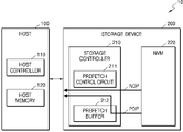
도 1은 본 개시의 일 실시예에 따른 스토리지 시스템(10)을 개략적으로 나타내는 블록도이다.1 is a block diagram schematically illustrating a
도 1을 참조하면, 스토리지 시스템(10)은 호스트(100) 및 스토리지 장치(200)를 포함할 수 있다. 스토리지 장치(200)는 스토리지 컨트롤러(210) 및 비휘발성 메모리(NVM)(220)를 포함할 수 있다. 실시예에 따라, 스토리지 컨트롤러(210)는 컨트롤러, 장치 컨트롤러 또는 메모리 컨트롤러로 지칭할 수도 있다. 실시예에 따라, 비휘발성 메모리(220)는 복수의 메모리 칩들 또는 복수의 메모리 다이들로 구현될 수 있다. 예를 들어, 복수의 메모리 칩들 각각은 DDP(Dual Die Package), QDP(Quadruple Die Package), 또는 ODP(Octuple Die Package)일 수 있다. 호스트(100)는 호스트 컨트롤러(110) 및 호스트 메모리(120)를 포함할 수 있다. 호스트 메모리(120)는 스토리지 장치(200)로 전송될 데이터, 혹은 스토리지 장치(200)로부터 전송된 데이터를 임시로 저장하기 위한 버퍼 메모리로서 기능할 수 있다.Referring to FIG. 1 , a
스토리지 장치(200)는 호스트(100)로부터의 요청에 따라 데이터를 저장하기 위한 저장 매체들을 포함할 수 있다. 일 예로서, 스토리지 장치(200)는 SSD(Solid State Drive), 임베디드(embedded) 메모리 및 착탈 가능한 외장(external) 메모리 중 적어도 하나를 포함할 수 있다. 스토리지 장치(200)가 SSD인 경우, 스토리지 장치(200)는 NVMe(non-volatile memory express) 표준을 따르는 장치일 수 있다. 스토리지 장치(200)가 임베디드 메모리 혹은 외장(external) 메모리인 경우, 스토리지 장치(200)는 UFS(universal flash storage) 혹은 eMMC(embedded multi-media card) 표준을 따르는 장치일 수 있다. 호스트(100)와 스토리지 장치(200)는 각각 채용된 표준 프로토콜에 따른 패킷을 생성하고 이를 전송할 수 있다.The
스토리지 장치(200)의 비휘발성 메모리(220)가 플래시 메모리를 포함할 때, 상기 플래시 메모리는 2D NAND 메모리 어레이 또는 3D(또는 수직형, Vertical) NAND(VNAND) 메모리 어레이를 포함할 수 있다. 다른 예로서, 스토리지 장치(200)는 다른 다양한 종류의 비휘발성 메모리들을 포함할 수도 있다. 예를 들어, 스토리지 장치(200)는 MRAM(Magnetic RAM), 스핀전달토크 MRAM(Spin-Transfer Torque MRAM), Conductive bridging RAM(CBRAM), FeRAM(Ferroelectric RAM), PRAM(Phase RAM), 저항 메모리(Resistive RAM) 및 다른 다양한 종류의 메모리가 적용될 수 있다. When the
스토리지 컨트롤러(210)는 호스트(100)로부터의 기입 요청에 응답하여 비휘발성 메모리(220)에 대한 데이터를 기입하도록 비휘발성 메모리(220)를 제어하거나, 또는 호스트(100)로부터의 독출 요청에 응답하여 비휘발성 메모리(220)에 저장된 데이터이 독출하도록 비휘발성 메모리(220)를 제어할 수 있다. 본 실시예에 따르면, 스토리지 컨트롤러(210)는 프리페치 제어 회로(211) 및 프리페치 버퍼(212)를 포함할 수 있다. 그러나, 본 발명은 이에 한정되지 않으며, 일부 실시예들에서, 프리페치 버퍼(212)는 스토리지 컨트롤러(210) 외부에 배치될 수도 있다.The
프리페치 제어 회로(211)는 비휘발성 메모리(220)에 대한 시퀀셜(sequential) 독출 동작 시, 데이터 프리페칭 동작을 동적으로 제어할 수 있다. 여기서, "시퀀셜 독출 동작"은 연속적인 어드레스들에 대응하는 독출 동작들을 나타낸다. 예를 들어, 스토리지 컨트롤러(210)가 호스트(100)로부터 제1 독출 커맨드 및 제1 어드레스를 수신하고, 이어서, 호스트(100)로부터 제2 독출 커맨드 및 제2 어드레스를 수신할 경우, 제2 어드레스의 시작점이 제1 어드레스의 마지막 LBA(Logical Block Address) 직후의 LBA에 대응할 수 있다. 이때, 스토리지 컨트롤러(210)는 제1 및 제2 독출 커맨드들에 대응하는 독출 동작을 시퀀셜 독출 동작이라고 판단할 수 있다. 여기서, "데이터 프리페칭 동작"은 호스트(100)로부터 아직 수신되지 않은 독출 커맨드 및 어드레스에 대응하는 데이터를 비휘발성 메모리(220)로부터 미리 독출하여 프리페치 버퍼(212)에 버퍼링하는 동작으로서, 시퀀셜 독출 동작 시, 데이터 프리페칭 동작을 통해 데이터 독출 성능을 향상시킬 수 있다.The
구체적으로, 프리페치 제어 회로(211)는 시퀀셜 독출 동작 시, 데이터 프리페칭 동작을 동적으로 제어함으로써, 비휘발성 메모리(220)로부터 호스트(100)로 제공되는 데이터의 전달 패쓰를, 노멀 데이터 패쓰(normal data path)(NDP) 또는 프리페치 데이터 패쓰(prefetch data path)(PDP)로 동적으로 선택할 수 있다. "노멀 데이터 패쓰(NDP)"는 호스트(100)로부터 수신되는 독출 커맨드 및 어드레스에 응답하여, 비휘발성 메모리(220)로부터 호스트(100)로 전달되는 데이터 전달 패쓰에 대응할 수 있다. "프리페치 데이터 패쓰(PDP)"는 스토리지 컨트롤러(210)에서 생성된 프리페치 커맨드에 응답하여, 비휘발성 메모리(220)로부터 프리페치 버퍼(212)로, 이어서 프리페치 버퍼(212)에서 호스트(100)로 전달되는 데이터 전달 패쓰에 대응할 수 있다. Specifically, the
도 2는 본 개시의 일 실시예에 따른 스토리지 장치(200)에서 프리페칭 동작을 인에이블한 경우, QD에 따른 시퀀셜 독출 성능을 예시적으로 나타낸다.2 exemplarily illustrates sequential read performance according to QD when a prefetch operation is enabled in the
도 1 및 도 2를 함께 참조하면, 가로축은 QD(Queueing Depth)를 나타내고, 세로축은 독출 성능을 나타낸다. 여기서, QD는 스토리지 컨트롤러(210)에서 동시에 대기 중인 입출력 요청들(I/O requests)의 개수를 나타낼 수 있다. 여기서, 독출 성능은, 단위 시간 동안 스토리지 장치(200)에서 호스트(100)로 전달되는 독출 데이터의 사이즈를 나타낼 수 있고, MB/s로 나타낼 수 있다. 일반적으로 시퀀셜 독출 동작 시, 프리페칭 동작의 인에이블을 통해 스토리지 장치(200)의 독출 성능을 향상시킬 수 있다. 이론적으로는, 독출 데이터의 사이즈가 커질수록 또는 QD가 높아질수록 프리페칭 동작의 인에이블을 통해 독출 성능이 선형적으로 증가할 수 있다. 그러나, 실제로는 프리페칭 동작의 인에이블 시, 특정 데이터 사이즈 또는 특정 QD 구간(21)에서는 독출 성능이 낮아질 수 있다.1 and 2 together, the horizontal axis represents queuing depth (QD), and the vertical axis represents read performance. Here, QD may indicate the number of input/output requests (I/O requests) waiting at the same time in the
본 실시예에 따르면, 프리페치 제어 회로(211)는 스토리지 장치(200)에서 호스트(100)로 전달되는 독출 데이터의 성능, 즉, 독출 성능에 기초하여, 프리페치 동작을 동적으로 인에이블 또는 디스에이블 시킴으로써 데이터 프리페칭 동작을 제어할 수 있다. 구체적으로, 프리페치 제어 회로(211)는 시퀀셜 독출 동작 시, 프리페치 동작을 인에이블 시키는 프리페치 인에이블 모드를 디폴트 모드로 결정하고, 주기적으로 프리페치 동작을 디스에이블 시킬 수 있다. 이때, 프리페치 제어 회로(211)는 프리페치 동작이 디스에이블된 프리페치 서스펜드(suspend) 모드에서의 독출 성능에 따라, 프리페치 서스펜드 모드를 유지하거나 프리페치 서스펜드 모드를 종료하고 프리페치 동작을 리쥼(resume)할 수 있다.According to the present embodiment, the
도 3은 본 개시의 일 실시예에 따라, 도 1의 스토리지 장치(200)를 예시적으로 나타낸다.3 exemplarily illustrates the
도 1 및 도 3을 함께 참조하면, 스토리지 컨트롤러(210)는 프리페치 제어 회로(211), 프리페치 버퍼(212), 판별기(213), 성능 모니터 회로(214), 인터벌 카운터(215), 호스트 인터페이스(interface, I/F)(216) 및 메모리 인터페이스(217)를 포함할 수 있다. 예를 들어, 프리페치 제어 회로(211), 성능 모니터 회로(214), 및 인터벌 카운터(215)는 하드웨어 로직으로 구현될 수 있다. 그러나, 본 발명은 이에 한정되지 않고, 프리페치 제어 회로(211), 성능 모니터 회로(214), 및 인터벌 카운터(215) 중 적어도 하나는 소프트웨어 또는 펌웨어로 구현될 수 있다. 도 1 및 도 2를 참조하여 상술된 내용은 본 실시예에도 적용될 수 있고, 중복된 설명은 생략하기로 한다.1 and 3 together, the
호스트 인터페이스(216)는 호스트(100)와 패킷(packet)을 송수신할 수 있다. 예를 들어, 호스트(100)로부터 호스트 인터페이스(216)로 전송되는 패킷은 독출 커맨드를 포함할 수 있으며, 호스트 인터페이스(216)로부터 호스트(100)로 전송되는 패킷은 비휘발성 메모리(220)로부터 독출된 데이터를 포함할 수 있다. 일 실시예에서, 호스트 인터페이스(216)는 호스트(100)로부터 복수의 패킷들을 순차적으로 수신할 수 있고, 각 패킷은 독출 커맨드 및 어드레스를 포함할 수 있다. 예를 들어, 스토리지 컨트롤러(210)는 복수의 패킷들 각각에 포함된 어드레스들에 따라, 독출 커맨드를 시퀀셜 독출 커맨드 또는 랜덤 독출 커맨드로 판단할 수 있다.The
스토리지 컨트롤러(210)는 독출 커맨드가 시퀀셜 독출 커맨드로 판단되면, 프리페치 제어 회로(211)의 프리페치 기능 또는 프리페치 동작을 인에이블 할 수 있다. 일 실시예에서, 스토리지 컨트롤러(210)는 연속된 독출 커맨드의 개수가 제1 기준치(REF1) 보다 크면 독출 커맨드를 시퀀셜 독출 커맨드로 판단할 수 있고, 연속된 독출 커맨드의 개수가 제1 기준치(REF1) 보다 크지 않으면 독출 커맨드를 랜덤 독출 커맨드로 판단할 수 있다. 예를 들어, 제1 기준치(REF1)는 2에 대응할 수 있고, 스토리지 컨트롤러(210)는 연속된 독출 커맨드의 개수가 2개보다 크면, 독출 커맨드를 시퀀셜 독출 커맨드로 판단할 수 있다. When it is determined that the read command is a sequential read command, the
일 실시예에서, 스토리지 컨트롤러(210)는 호스트(100)로부터 제1 독출 커맨드 및 제1 어드레스를 수신하고, 이어서, 제2 독출 커맨드 및 제2 어드레스를 수신하는 경우, 제1 및 제2 어드레스들에 따라 제1 및 제2 독출 커맨드들을 시퀀셜 독출 커맨드들 또는 랜덤 독출 커맨드들로 판단할 수 있다. 예를 들어, 제1 어드레스와 제2 어드레스가 연속하는 경우, 스토리지 컨트롤러(210)는 제1 및 제2 독출 커맨드들을 시퀀셜 독출 커맨드들로 판단할 수 있다. 일 실시예에서, 스토리지 컨트롤러(210)는 호스트(100)로부터 시퀀셜 독출 커맨드를 정의하는 플래그 및 독출 커맨드를 포함하는 커맨드 세트(set)를 수신할 수 있다. 이때, 스토리지 컨트롤러(210)는 수신된 독출 커맨드를 시퀀셜 독출 커맨드로 판단할 수 있다.In an embodiment, when the
독출 커맨드가 시퀀셜 독출 커맨드로 판단된 경우, 프리페치 제어 회로(211)는 프리패치 기능 또는 프리페치 동작을 인에이블할 수 있고, 프리페치 요청 신호(REQ_PRF)를 메모리 인터페이스(217)에 제공할 수 있다. 예를 들어, 프리페치 제어 회로(211)는 독출 커맨드가 시퀀셜 독출 커맨드로 판단되면, 프리페치 동작을 인에이블할 수 있고, 프리페치 요청 신호(REQ_PRF)를 메모리 인터페이스(217)에 제공할 수 있다. 예를 들어, 프리페치 제어 회로(211)는 독출 커맨드가 랜덤 독출 커맨드로 판단되면, 프리페치 동작을 디스에이블할 수 있고, 프리페치 요청 신호(REQ_PRF)를 메모리 인터페이스(217)에 제공하지 않을 수 있다.When it is determined that the read command is a sequential read command, the
일 실시예에서, 프리페치 제어 회로(211)는 호스트(100)로부터 수신된 독출 커맨드에 응답한 비휘발성 메모리(220)의 독출 동작 중에 또는 비휘발성 메모리(220)로부터 독출 데이터가 수신되는 동안에, 프리페치 요청 신호(REQ_PRF)를 메모리 인터페이스(217)에 제공할 수 있다. 일 실시예에서, 프리페치 제어 회로(211)는 이전 프리페치 요청 신호(REQ_PRF)에 응답한 비휘발성 메모리(220)의 프리페치 동작 중에 또는 비휘발성 메모리(220)로부터 프리페치 데이터가 수신되는 동안에, 다음 프리페치 요청 신호(REQ_PRF)를 메모리 인터페이스(217)에 제공할 수 있다. In an embodiment, the
메모리 인터페이스(217)는 비휘발성 메모리(220)에 기록될 데이터를 비휘발성 메모리(220)로 송신하거나, 비휘발성 메모리(220)의 메모리 셀 어레이(221)로부터 독출된 데이터를 수신할 수 있다. 이러한 메모리 인터페이스(217)는 토글(Toggle) 혹은 온파이(Open NAND Flash Interface; ONFI)와 같은 표준 규약을 준수하도록 구현될 수 있다. 메모리 인터페이스(217)는 복수의 데이터 라인들 또는 복수의 입출력 라인들을 통해 비휘발성 메모리(220)와 연결될 수 있다. 예를 들어, 복수의 데이터 라인들 또는 복수의 입출력 라인들은 하나의 채널에 대응할 수 있다. 예를 들어, 복수의 데이터 라인들의 개수는 8개일 수 있으나, 본 발명은 이에 한정되지 않는다.The
일 실시예에서, 메모리 인터페이스(217)는 호스트(100)로부터 수신한 독출 커맨드로부터 독출 커맨드를 생성할 수 있고, 생성된 독출 커맨드를 비휘발성 메모리(220)에 전송할 수 있다. 예를 들어, 메모리 인터페이스(217)는 복수의 데이터 라인들을 통해 독출 커맨드를 비휘발성 메모리(220)에 전송할 수 있다. 또한, 메모리 인터페이스(217)는 복수의 데이터 라인들을 통해 비휘발성 메모리(220)로부터 데이터를 수신할 수 있다. 이때, 독출 커맨드에 응답하여 수신되는 데이터는 "노멀 데이터(normal data)(D_N)"라고 지칭할 수 있다.In an embodiment, the
일 실시예에서, 메모리 인터페이스(217)는 프리페치 제어 회로(211)로부터 수신한 프리페치 요청 신호(REQ_PRF)로부터 프리페치 커맨드를 생성할 수 있고, 생성된 프리페치 커맨드를 비휘발성 메모리(220)에 전송할 수 있다. 예를 들어, 메모리 인터페이스(217)는 복수의 데이터 라인들을 통해 프리페치 커맨드를 비휘발성 메모리(220)에 전송할 수 있다. 또한, 메모리 인터페이스(217)는 복수의 데이터 라인들을 통해 비휘발성 메모리(220)로부터 데이터를 수신할 수 있다. 이때, 프리페치 요청 신호(REQ_PRF)에 응답하여 비휘발성 메모리(220)로부터 수신되는 데이터는 "프리페치 데이터(prefetched data)(D_P)"라고 지칭할 수 있다.In an embodiment, the
프리페치 버퍼(212)는 비휘발성 메모리(220)로부터 프리페치된 프리페치 데이터(D_P)를 버퍼링할 수 있다. 판별기(213)는 메모리 인터페이스(217)로부터 수신되는 노멀 데이터(D_N) 및 프리페치 버퍼(212)로부터 수신되는 프리페치 데이터(D_P) 중 하나를 독출 데이터(D_R)로 선택할 수 있고, 선택된 독출 데이터(D_R)를 호스트 인터페이스(216)에 제공할 수 있다. 예를 들어, 시퀀셜 독출 커맨드의 어드레스, 즉, 시퀀셜 독출 커맨드의 LBA(Logical Block Address)가, 프리페치 버퍼(212)에 버퍼링된 프리페치 데이터(D_P)의 어드레스, 즉, 프리페치 데이터(D_P)의 LBA에 대응하면, 판별기(213)는 프리페치 데이터(D_P)를 독출 데이터(D_R)로서 선택할 수 있다. 예를 들어, 시퀀셜 독출 커맨드의 LBA가 프리페치 버퍼(212)에 버퍼링된 프리페치 데이터(D_P)의 LBA에 대응하지 않으면, 판별기(213)는 노멀 데이터(D_N)를 독출 데이터(D_R)로서 선택할 수 있다.The
성능 모니터 회로(214)는 판별기(213)에서 호스트 인터페이스(216)로 전달되는 독출 데이터(D_R)의 성능을 모니터링함으로써 성능 신호(Performance Signal, PS)를 생성할 수 있고, 생성된 성능 신호(PS)를 프리페치 제어 회로(211)에 실시간으로 제공할 수 있다. 성능 신호(PS)는 독출 성능에 대응할 수 있고, 독출 성능은 단위 시간 당 전달되는 독출 데이터(D_R)의 사이즈에 대응할 수 있다.The
인터벌 카운터(215)는 미리 정의된 주기마다 인터벌 신호(Interval Signal)(IS)를 생성할 수 있고, 생성된 인터벌 신호(TS)를 프리페치 제어 회로(211)에 제공할 수 있다. 예를 들어, 인터벌 카운터(215)는 클럭 신호로부터 클럭 개수를 카운팅하고, 카운팅된 클럭 개수가 미리 정의된 주기에 대응하는 경우, 인터벌 신호(IS)를 활성화할 수 있다. 예를 들어, 인터벌 신호(IS)는 펄스 신호로 생성될 수 있다. 실시예에 따라, 인터벌 카운터(215)는 타이머 또는 인터벌 타이머로 지칭될 수 있다. The
독출 커맨드가 시퀀셜 독출 커맨드로 판단된 경우, 프리페치 제어 회로(211)는 프리페치 요청 신호(REQ_PRF)를 생성할 수 있다. 본 실시예에서, 프리페치 제어 회로(211)는 시퀀셜 독출 동작 시, 프리페치 요청 신호(REQ_PRF)를 인에이블 레벨로 생성하고, 이에 따라, 프리페치 인에이블 모드를 디폴트 모드로 결정할 수 있다. When it is determined that the read command is a sequential read command, the
프리페치 제어 회로(211)는 인터벌 카운터(215)로부터 수신된 인터벌 신호(IS)에 응답하여 프리페치 요청 신호(REQ_PRF)을 생성할 수 있다. 일 실시예에서, 프리페치 제어 회로(211)는 인터벌 카운터(215)로부터 수신된 인터벌 신호(IS)에 응답하여, 성능 신호(PS)가 제1 임계치(TH1) 이하이면 프리페치 요청 신호(REQ_PRF)를 인에이블 레벨로 생성할 수 있다. 일 실시예에서, 프리페치 제어 회로(211)는 인터벌 카운터(215)로부터 수신된 인터벌 신호(IS)에 응답하여, 성능 신호(PS)가 제1 임계치(TH1) 보다 크면 프리페치 요청 신호(REQ_PRF)를 디스에이블 레벨로 생성할 수 있다. 판별기(213)는 프리페치 버퍼(212)에 버퍼링된 프리페치 데이터(D_P)를 선택하고, 프리페치 데이터(D_P)를 독출 데이터(D_R)로서 출력할 수 있다.The
도 4는 본 개시의 일 실시예에 따라, 스토리지 장치(200)의 시간에 따른 독출 성능을 나타내는 그래프이다.4 is a graph illustrating read performance over time of the
도 4를 참조하면, 가로축은 시간을 나타내고, 세로축은 독출 성능을 나타낸다. 예를 들어, 독출 성능은 도 3의 성능 모니터 회로(214)에서 생성되는 성능 신호(PS)에 대응할 수 있다. 이하에서는, 도 3 및 도 4를 함께 참조하여 스토리지 장치(200)의 프리페치 제어 동작을 설명하기로 한다.Referring to FIG. 4 , the horizontal axis represents time, and the vertical axis represents read performance. For example, the read performance may correspond to the performance signal PS generated by the
프리페치 인에이블 구간(41)은 프리페치 동작인 인에이블된 구간을 나타내고, 프리페치 디스에이블 구간(42)은 프리페치 동작이 디스에이블된 구간을 나타낸다. 예를 들어, 프리페치 인에이블 구간(41)은 t1 시점에서 t4 시점까지의 시간 구간에 대응할 수 있고, 프리페치 디스에이블 구간(42)은 t4 시점부터의 시간 구간에 대응할 수 있다. 프리페치 제어 회로(211)는 시퀀셜 독출 동작 시, 프리페치 요청 신호(REQ_PRF)를 디폴트 레벨인 인에이블 레벨로 결정할 수 있다. 성능 신호(PS)가 제1 임계치(TH1) 보다 크면, 프리페치 제어 회로(211)는 프리페치 요청 신호(REQ_PRF)를 인에이블 레벨에서 디스에이블 레벨로 변경할 수 있다.The prefetch enable
일 실시예에서, 프리페치 제어 회로(211)는 인터벌 신호(IS)에 따라 프리페치 요청 신호(REQ_PRF)를 주기적으로 서스펜드할 수 있다. 인터벌 신호(IS)가 활성화되면, 프리페치 제어 회로(211)는 프리페치 요청 신호(REQ_PRF)를 디스에이블 레벨로 결정할 수 있고, 이에 따라, 프리페치 모드는 프리페치 인에이블 모드에서 프리페치 서스펜드 모드로 변경될 수 있다. 이에 따라, 판별기(213)는 메모리 인터페이스(217)로부터 수신되는 노멀 데이터(D_N)를 선택하고, 노멀 데이터(D_N)를 독출 데이터(D_R)로서 출력할 수 있다.In an embodiment, the
t2 시점에서, 인터벌 신호(IS)가 활성화되면, 프리페치 제어 회로(211)는 프리페치 요청 신호(REQ_PRF)를 디스에이블 레벨로 생성하고, 성능 신호(PS)를 제1 임계치(TH1)과 비교할 수 있다. 비교 결과, 성능 신호(PS)가 제1 임계치(TH1) 보다 크지 않으면, 프리페치 제어 회로(211)는 프리페치 서스펜드 모드를 종료하고, 프리페치 요청 신호(REQ_PRF)를 인에이블 레벨로 변경할 수 있다. 이에 따라, 판별기(213)는 프리페치 데이터(D_P)를 출력할 수 있다. At time t2, when the interval signal IS is activated, the
t3 시점에서, 인터벌 신호(IS)가 활성화되면, 프리페치 제어 회로(211)는 프리페치 요청 신호(REQ_PRF)를 디스에이블 레벨로 생성하고, 성능 신호(PS)를 제1 임계치(TH1)과 비교할 수 있다. 이때, t2 시점과 t3 시점 사이의 시간 간격은 제1 주기(PR1)에 대응할 수 있고, 인터벌 카운터(215)는 제1 주기(PR1)마다 인터벌 신호(IS)를 활성화시킬 수 있다. 이와 같이, 프리페치 인에이블 구간(41)에서, 프리페치 제어 회로(211)는 제1 주기(PR1)마다 프리페치 요청 신호(REQ_PRF)를 디스에이블 레벨로 생성하고, 성능 신호(PS)를 제1 임계치(TH1)과 비교할 수 있다. 비교 결과, 성능 신호(PS)가 제1 임계치(TH1) 보다 크면, 프리페치 디스에이블 구간(42)에 진입할 수 있다.At time t3, when the interval signal IS is activated, the
t4 시점에서, 프리페치 제어 회로(211)는 프리페치 요청 신호(REQ_PRF)를 디스에이블 레벨로 생성하고, 판별기(213)는 노멀 데이터(D_N)를 출력할 수 있다. 프리페치 디스에이블 구간(42)에서, 프리페치 제어 회로(211)는 제2 주기(PR2)마다 성능 신호(PS)를 제1 임계치(TH1)과 비교할 수 있다. 프리페치 제어 회로(211)는 t5 시점 및 t6 시점에서, 성능 신호(PS)를 제1 임계치(TH1)과 비교할 수 있다. 이때, t5 시점과 t6 시점 사이의 시간 간격은 제2 주기(PR2)에 대응할 수 있고, 인터벌 카운터(215)는 제2 주기(PR2)마다 인터벌 신호(IS)를 활성화시킬 수 있다. 예를 들어, 제1 주기(PR1)와 제2 주기(PR2)는 동일할 수 있다. 그러나, 본 발명은 이에 한정되지 않으며, 제1 주기(PR1)와 제2 주기(PR2)는 서로 다를 수도 있다.At time t4 , the
비교 결과, 성능 신호(PS)가 제1 임계치(TH1) 보다 크면, 프리페치 제어 회로(211)는 프리페치 디스에이블 구간(42)을 유지할 수 있다. 한편, 비교 결과, 성능 신호(PS)가 제1 임계치(TH1) 보다 크지 않으면, 프리페치 제어 회로(211)는 프리페치 모드를 프리페치 인에이블 모드로 변경하고, 프리페치 요청 신호(REQ_PRF)를 인에이블 레벨로 생성할 수 있다. 이때, 판별기(213)는 프리페치 데이터(D_P)를 출력할 수 있다.As a result of the comparison, if the performance signal PS is greater than the first threshold TH1 , the
일 실시예에서, 프리페치 제어 회로(211)는 프리페치 인에이블 구간(41)에서 성능 신호(PS)를 제2 임계치(예를 들어, 도 9의 TH2)과 주기적으로 비교할 수 있다. 여기서, 제2 임계치(TH2)는 제1 임계치(TH1) 보다 작을 수 있다. 비교 결과, 성능 신호(PS)가 제2 임계치(TH2) 보다 크면, 프리페치 제어 회로(211)는 프리페치 동작을 주기적으로 서스펜드할 수 있다. 다시 말해, 프리페치 제어 회로(211)는 성능 신호(PS)가 제2 임계치(TH2) 보다 큰 시점부터, 프리페치 동작을 주기적으로 서스펜드할 수 있다. 이에 대해, 도 8 및 도 9를 참조하여 더욱 상세하게 설명하기로 한다.In an embodiment, the
도 5는 본 개시의 일 실시예에 따른 스토리지 컨트롤러의 동작 방법을 나타내는 흐름도이다.5 is a flowchart illustrating a method of operating a storage controller according to an embodiment of the present disclosure.
도 5를 참조하면, 본 실시예에 따른 스토리지 컨트롤러의 동작 방법은 비휘발성 메모리에 대한 시퀀셜 독출 동작 시, 스토리지 컨트롤러가 데이터 프리페칭 동작을 제어하는 방법으로서, 예를 들어, 도 3의 스토리지 컨트롤러(210)에 의해 수행될 수 있다. 이하에서는, 도 1, 도 3 및 도 5를 함께 참조하여 설명하기로 한다. Referring to FIG. 5 , the method of operating the storage controller according to the present exemplary embodiment is a method in which the storage controller controls a data prefetching operation during a sequential read operation of a nonvolatile memory. For example, the storage controller ( 210) can be performed. Hereinafter, it will be described with reference to FIGS. 1, 3 and 5 together.
단계 S110에서, 스토리지 컨트롤러(210)는 시퀀셜 독출 커맨드를 기초로, 비휘발성 메모리(220)로부터 프리페칭된 프리페치 데이터(D_P)를 프리페치 버퍼(212)에 버퍼링한다. 단계 S120에서, 비휘발성 메모리(220)에 대한 시퀀셜 독출 동작 시, 스토리지 컨트롤러(210)는 프리페치 데이터(D_P)를 독출 데이터(D_R)로서 출력한다. 단계 S130에서, 스토리지 컨트롤러(210)는 제1 시점에서, 비휘발성 메모리(220)로부터 독출되는 노멀 데이터(D_N)를 독출 데이터(D_R)로서 출력한다. 단계 S140에서, 스토리지 컨트롤러(210)는 프리페치 서스펜드 구간에서, 독출 데이터(D_R)의 성능을 기초로 프리페치 데이터(D_P) 또는 노멀 데이터(D_N)를 독출 데이터(D_R)로서 출력한다.In operation S110 , the
도 6은 본 개시의 일 실시예에 따른 스토리지 컨트롤러의 프리페치 제어 방법을 나타내는 흐름도이다.6 is a flowchart illustrating a prefetch control method of a storage controller according to an embodiment of the present disclosure.
도 6을 참조하면, 본 실시예에 따른 스토리지 컨트롤러의 프리페치 제어 방법은 도 5의 단계 S130 및 S140의 일 구현 예에 대응할 수 있고, 예를 들어, 도 3의 프리페치 제어 회로(211)에서 수행되는 시계열적인 단계들을 포함할 수 있다. 이하에서는, 도 3 내지 도 6을 함께 참조하여 설명하기로 한다. 예를 들어, 단계 S210은 도 5의 S120 이후에 수행될 수 있다. Referring to FIG. 6 , the prefetch control method of the storage controller according to the present embodiment may correspond to an implementation example of steps S130 and S140 of FIG. 5 , and for example, in the
단계 S210에서, 스토리지 컨트롤러(210)는 미리 결정된 주기 시간의 경과 여부를 판단한다. 예를 들어, 미리 결정된 주기 시간은 도 4의 제1 주기(PR1)에 대응할 수 있다. 일 실시예에서, 스토리지 컨트롤러(210)는 프리페치 인에이블 구간(41)에 진입한 시점부터 주기 시간의 경과 여부를 판단할 수 있다. 일 실시예에서, 스토리지 컨트롤러(210)는 프리페치 인에이블 구간(41)에 진입한 이후, 성능 신호(PS)가 제2 임계치(TH2) 보다 큰 시점부터 주기 시간의 경과 여부를 판단할 수 있다.In step S210 , the
판단 결과, 주기 시간이 경과되면, 단계 S220에서, 스토리지 컨트롤러(210)는 프리페치 요청 신호(REQ_PRF)를 디스에이블 레벨로 생성하고, 데이터 프리페칭 동작을 디스에이블 시킨다. 이에 따라, 판별기(213)는 노멀 데이터(D_N)를 독출 데이터(D_R)로서 출력한다. 단계 S230에서, 스토리지 컨트롤러(210)는 독출 데이터(D_R)의 성능, 즉, 노멀 데이터(D_N)의 성능을 체크한다. 단계 S240에서, 스토리지 컨트롤러(210)는 성능이 제1 임계치(TH1) 보다 큰지 판단한다. 판단 결과, 성능이 제1 임계치(TH1) 보다 크지 않으면, 스토리지 컨트롤러(210)는 프리페치 요청 신호(REQ_PRF)를 인에이블 레벨로 생성하고, 데이터 프리페칭 동작을 인에이블 시킨다. As a result of the determination, when the cycle time has elapsed, in step S220 , the
도 7은 본 개시의 일 실시예에 따라, 도 6의 프리페치 제어 동작을 예시적으로 나타내는 그래프이다.7 is a graph exemplarily illustrating a prefetch control operation of FIG. 6 , according to an embodiment of the present disclosure.
도 7을 참조하면, 가로축은 시간을 나타내고, 세로축은 성능을 나타낸다. 도 7에서는, 제1 QD(QD_A)에서의 독출 성능 및 제2 QD(QD_B)에서의 독출 성능이 예시되었다. 제1 QD(QD_A)와 제2 QD(QD_B)는 서로 다른 임의의 QD들에 대응할 수 있다. 이하에서는, 도 3, 도 6 및 도 7을 함께 참조하여 설명하기로 한다.Referring to FIG. 7 , the horizontal axis represents time, and the vertical axis represents performance. 7 , the read performance in the first QD (QD_A) and the read performance in the second QD (QD_B) are exemplified. The first QD (QD_A) and the second QD (QD_B) may correspond to different random QDs. Hereinafter, it will be described with reference to FIGS. 3, 6 and 7 together.
제1 QD(QD_A)의 경우, t10 시점부터 t11 시점까지의 구간에서, 프리페치 요청 신호(REQ_PRF)는 인에이블 레벨일 수 있다. 예를 들어, t10 시점부터 t11 시점까지의 구간은 미리 결정된 주기(예를 들어, 도 4의 제1 주기(PR1))에 대응할 수 있다. t11 시점에서, 프리페치 제어 회로(211)는 프리페치 요청 신호(REQ_PRF)을 디스에이블 레벨로 변경할 수 있고, 판별기(213)는 노멀 데이터(D_N)를 독출 데이터(D_R)로서 출력할 수 있다. 이후 t12 시점에서, 프리페치 제어 회로(211)는 독출 데이터(D_R)의 독출 성능, 즉, 성능 신호(PS)를 체크할 수 있다. In the case of the first QD (QD_A), in a period from time t10 to time t11, the prefetch request signal REQ_PRF may be at an enable level. For example, a section from time t10 to time t11 may correspond to a predetermined period (eg, the first period PR1 of FIG. 4 ). At time t11 , the
성능 신호(PS)가 제1 임계치(TH1) 보다 크면, 프리페치 제어 회로(211)는 프리페치 요청 신호(REQ_PRF)를 디스에이블 레벨로 유지할 수 있다. 이어서, t13 시점 및 t15 시점에서, 프리페치 요청 신호(REQ_PRF)는 디스에이블 레벨일 수 있고, 판별기(213)는 노멀 데이터(D_N)를 독출 데이터(D_R)로서 출력할 수 있다. 이때, t14 시점 및 t16 시점에서, 프리페치 제어 회로(211)는 독출 데이터(D_R)의 독출 성능, 즉, 성능 신호(PS)를 체크할 수 있다. 예를 들어, t11 시점부터 t13 시점까지의 구간, t13 시점에서 t15 시점까지의 구간은 미리 결정된 주기(예를 들어, 도 4의 제2 주기(PR2))에 대응할 수 있다.When the performance signal PS is greater than the first threshold TH1 , the
제2 QD(QD_B)의 경우, t10 시점부터 t11 시점까지의 구간에서, 프리페치 요청 신호(REQ_PRF)는 인에이블 레벨일 수 있다. 예를 들어, t10 시점부터 t11 시점까지의 구간은 미리 결정된 주기에 대응할 수 있다. t11 시점에서, 프리페치 제어 회로(211)는 프리페치 요청 신호(REQ_PRF)를 디스에이블 레벨로 변경할 수 있고, 판별기(213)는 노멀 데이터(D_N)를 독출 데이터(D_R)로서 출력할 수 있다. 이때, 프리페치 제어 회로(211)는 독출 데이터(D_R)의 독출 성능, 즉, 성능 신호(PS)를 체크할 수 있다. In the case of the second QD (QD_B), in a period from time t10 to time t11, the prefetch request signal REQ_PRF may be at an enable level. For example, a section from time t10 to time t11 may correspond to a predetermined period. At time t11 , the
성능 신호(PS)가 제1 임계치(TH1) 보다 크지 않으면, t12 시점에, 프리페치 제어 회로(211)는 프리페치 요청 신호(REQ_PRF)를 인에이블 레벨로 변경할 수 있고, 판별기(213)는 프리페치 데이터(D_P)를 독출 데이터(D_R)로서 출력할 수 있다. 이어서, t13 시점에서, 프리페치 제어 회로(211)는 프리페치 요청 신호(REQ_PRF)를 디스에이블 레벨로 변경할 수 있고, 판별기(213)는 노멀 데이터(D_N)를 독출 데이터(D_R)로서 출력할 수 있다. 이때, 프리페치 제어 회로(211)는 독출 데이터(D_R)의 독출 성능, 즉, 성능 신호(PS)를 체크할 수 있다. 성능 신호(PS)가 제1 임계치(TH1) 보다 크지 않으면, t14 시점에, 프리페치 제어 회로(211)는 프리페치 요청 신호(REQ_PRF)를 인에이블 레벨로 변경할 수 있고, 판별기(213)는 프리페치 데이터(D_P)를 독출 데이터(D_R)로서 출력할 수 있다.If the performance signal PS is not greater than the first threshold TH1, at time t12, the
도 8은 본 개시의 일 실시예에 따른 스토리지 컨트롤러의 프리페치 제어 방법을 나타내는 흐름도이다.8 is a flowchart illustrating a prefetch control method of a storage controller according to an embodiment of the present disclosure.
도 8을 참조하면, 본 실시예에 따른 스토리지 컨트롤러의 프리페치 제어 방법은 도 5의 단계 S130 및 S140의 일 구현 예에 대응할 수 있고, 예를 들어, 도 3의 프리페치 제어 회로(211)에서 수행되는 시계열적인 단계들을 포함할 수 있다. 이하에서는, 도 3 및 도 8을 함께 참조하여 설명하기로 한다. 예를 들어, 단계 S310은 도 5의 S120 이후에 수행될 수 있다. Referring to FIG. 8 , the prefetch control method of the storage controller according to the present embodiment may correspond to an implementation example of steps S130 and S140 of FIG. 5 , and for example, in the
단계 S310에서, 스토리지 컨트롤러(210)는 독출 성능이 제2 임계치(TH2) 보다 큰지 판단한다. 일 실시예에서, 스토리지 컨트롤러(210)는 독출 성능이 제2 임계치(TH2) 보다 큰지 주기적으로 판단할 수 있다. 예를 들어, 스토리지 컨트롤러(210)는 프리페치 인에이블 구간(41)에 진입한 시점부터 주기적으로 독출 성능을 제2 임계치(TH2)와 비교할 수 있다.In operation S310 , the
판단 결과, 독출 성능이 제2 임계치(TH2) 보다 크면, 단계 S320에서, 스토리지 컨트롤러(210)는 프리페치 요청 신호(REQ_PRF)를 디스에이블 레벨로 생성하고, 데이터 프리페칭 동작을 디스에이블 시킨다. 이에 따라, 판별기(213)는 노멀 데이터(D_N)를 독출 데이터(D_R)로서 출력한다. 단계 S330에서, 스토리지 컨트롤러(210)는 독출 데이터(D_R)의 성능, 즉, 노멀 데이터(D_N)의 성능을 체크한다. 단계 S340에서, 스토리지 컨트롤러(210)는 성능이 제1 임계치(TH1) 보다 큰지 판단한다. 판단 결과, 성능이 제1 임계치(TH1) 보다 크지 않으면, 스토리지 컨트롤러(210)는 프리페치 요청 신호(REQ_PRF)을 인에이블 레벨로 생성하고, 데이터 프리페칭 동작을 인에이블 시킨다. As a result of the determination, if the read performance is greater than the second threshold TH2 , in operation S320 , the
도 9는 본 개시의 일 실시예에 따라, 도 8의 프리페치 제어 동작을 예시적으로 나타내는 그래프이다.9 is a graph exemplarily illustrating a prefetch control operation of FIG. 8 , according to an embodiment of the present disclosure.
도 9를 참조하면, 가로축은 시간을 나타내고, 세로축은 성능을 나타낸다. 도 9에서는, 제1 QD(QD_A)에서의 독출 성능 및 제2 QD(QD_B)에서의 독출 성능이 예시되었다. 제1 QD(QD_A)와 제2 QD(QD_B)는 서로 다른 임의의 QD들에 대응할 수 있다. 이하에서는, 도 3, 도 8 및 도 9를 함께 참조하여 설명하기로 한다.Referring to FIG. 9 , the horizontal axis represents time, and the vertical axis represents performance. In FIG. 9 , the read performance in the first QD (QD_A) and the read performance in the second QD (QD_B) are exemplified. The first QD (QD_A) and the second QD (QD_B) may correspond to different random QDs. Hereinafter, it will be described with reference to FIGS. 3, 8 and 9 together.
제1 QD(QD_A)의 경우, t20 시점부터 t21 시점까지의 구간에서, 프리페치 요청 신호(REQ_PRF)는 인에이블 레벨일 수 있고, 프리페치 제어 회로(211)는 독출 성능을 제2 임계치(TH2)와 주기적으로 비교할 수 있다. t21 시점에서, 독출 성능이 제2 임계치(TH2) 보다 크면, 프리페치 제어 회로(211)는 프리페치 요청 신호(REQ_PRF)를 디스에이블 레벨로 변경할 수 있고, 판별기(213)는 노멀 데이터(D_N)를 독출 데이터(D_R)로서 출력할 수 있다. 이때, 프리페치 제어 회로(211)는 독출 데이터(D_R)의 독출 성능, 즉, 성능 신호(PS)를 체크할 수 있다. In the case of the first QD (QD_A), in the period from time t20 to time t21, the prefetch request signal REQ_PRF may be at an enable level, and the
성능 신호(PS)가 제1 임계치(TH1) 보다 크면, 프리페치 제어 회로(211)는 프리페치 요청 신호(REQ_PRF)는 디스에이블 레벨로 유지할 수 있다. 이어서, t23 시점 및 t25 시점에서, 프리페치 요청 신호(REQ_PRF)는 디스에이블 레벨일 수 있고, 판별기(213)는 노멀 데이터(D_N)을 독출 데이터(D_R)로서 출력할 수 있다. 이때, t24 및 t26 시점에, 독출 데이터(D_R)의 독출 성능, 즉, 성능 신호(PS)를 체크할 수 있다. 예를 들어, t21 시점부터 t23 시점까지의 구간, t23 시점에서 t25 시점까지의 구간은 미리 결정된 주기에 대응할 수 있다.When the performance signal PS is greater than the first threshold TH1 , the
제2 QD(QD_B)의 경우, t20 시점부터 t21 시점까지의 구간에서, 프리페치 요청 신호(REQ_PRF)는 인에이블 레벨일 수 있고, 프리페치 제어 회로(211)는 독출 성능을 제2 임계치(TH2)와 주기적으로 비교할 수 있다. t21 시점에서, 독출 성능이 제2 임계치(TH2) 보다 크면, 프리페치 제어 회로(211)는 프리페치 요청 신호(REQ_PRF)를 디스에이블 레벨로 변경할 수 있고, 판별기(213)는 노멀 데이터(D_N)를 독출 데이터(D_R)로서 출력할 수 있다. 이때, 프리페치 제어 회로(211)는 독출 데이터(D_R)의 독출 성능, 즉, 성능 신호(PS)를 체크할 수 있다. In the case of the second QD (QD_B), in the period from time t20 to time t21, the prefetch request signal REQ_PRF may be at an enable level, and the
성능 신호(PS)가 제1 임계치(TH1) 보다 크지 않으면, t22 시점에, 프리페치 제어 회로(211)는 프리페치 요청 신호(REQ_PRF)를 인에이블 레벨로 변경할 수 있고, 판별기(213)는 프리페치 데이터(D_P)를 독출 데이터(D_R)로서 출력할 수 있다. 이어서, t23 시점에서, 프리페치 제어 회로(211)는 프리페치 요청 신호(REQ_PRF)를 디스에이블 레벨로 변경할 수 있고, 판별기(213)는 노멀 데이터(D_N)를 독출 데이터(D_R)로서 출력할 수 있다. 이때, t24 시점에 프리페치 제어 회로(211)는 독출 데이터(D_R)의 독출 성능, 즉, 성능 신호(PS)를 체크할 수 있다. 성능 신호(PS)가 제1 임계치(TH1) 보다 크지 않으면, 프리페치 제어 회로(211)는 프리페치 요청 신호(REQ_PRF)를 인에이블 레벨로 변경할 수 있고, 판별기(213)는 프리페치 데이터(D_P)를 독출 데이터(D_R)로서 출력할 수 있다.If the performance signal PS is not greater than the first threshold TH1, at time t22, the
도 10은 본 개시의 일 실시예에 따른 스토리지 장치의 동작 방법을 나타내는 그래프이다.10 is a graph illustrating a method of operating a storage device according to an embodiment of the present disclosure.
도 10을 참조하면, 본 실시예에 따른 스토리지 장치의 동작 방법은 비휘발성 메모리에 대한 시퀀셜 독출 동작 시 스토리지 장치가 데이터 프리페칭 동작을 제어함으로써 독출 동작을 수행하는 방법으로서, 예를 들어, 도 3의 스토리지 장치(200)에서 수행될 수 있다. 이하에서는, 도 1, 도 3 및 도 10을 함께 참조하여 설명하기로 한다.Referring to FIG. 10 , a method of operating a storage device according to the present exemplary embodiment is a method of performing a read operation by controlling a data prefetching operation by the storage device during a sequential read operation of a nonvolatile memory. For example, FIG. 3 . may be performed in the
단계 S400에서, 호스트(100)로부터 수신된 시퀀셜 독출 커맨드를 기초로, 스토리지 컨트롤러(210)에서 비휘발성 메모리(220)에 프리페치 커맨드를 전송한다. 단계 S410에서, 프리페치 커맨드에 응답하여 비휘발성 메모리(220)로부터 프리페칭된 프리페치 데이터(D_P)를 프리페치 버퍼(212)에 버퍼링한다. 단계 S420에서, 호스트(100)로부터 수신된 시퀀셜 독출 커맨드를 기초로, 스토리지 컨트롤러(210)에서 호스트(100)로, 프리페치 버퍼(212)에 버퍼링된 프리페치 데이터(D_P)를 전달한다. 단계 S430에서, 제1 시간이 경과하면, 스토리지 컨트롤러(210)에서 호스트(100)로, 비휘발성 메모리(220)로부터 수신되는 노멀 데이터(D_N)를 전달한다. 단계 S440에서, 노멀 데이터(D_N)의 독출 성능이 제1 임계치(TH1) 이하이면, 스토리지 컨트롤러(210)에서 호스트(100)로, 프리페치 데이터(D_P)를 전달한다. 실시예에 따라, 노멀 데이터(D_N)의 독출 성능이 제1 임계치(TH1) 보다 크면, 스토리지 컨트롤러(210)에서 호스트(100)로, 노멀 데이터(N_P)를 전달할 수 있다.In operation S400 , the
도 11은 본 개시의 일 실시예에 따른 호스트(100)와 스토리지 장치(200)의 동작을 나타내는 흐름도이다.11 is a flowchart illustrating operations of the
도 11을 참조하면, 단계 S510에서, 호스트(100)는 스토리지 장치(200)에 독출 커맨드를 전송한다. 예를 들어, 호스트(100)는 독출 커맨드 및 어드레스를 포함하는 패킷을 스토리지 장치(200)에 전송할 수 있다. 단계 S520에서, 스토리지 장치(200)는 독출 커맨드에 응답하여 독출 동작을 수행한다. 단계 S530에서, 스토리지 장치(200)는 노멀 데이터(D_N)를 호스트(100)에 전송한다. 예를 들어, 스토리지 장치(200)는 노멀 데이터(D_N)를 포함하는 패킷을 호스트(100)에 전송할 수 있다. 단계 S510 내지 S530은 반복적으로 수행될 수 있다. 예를 들어, 호스트(100)는 복수의 독출 커맨드들을 순차적으로 스토리지 장치(200)에 전송할 수 있다.Referring to FIG. 11 , in step S510 , the
단계 S540에서, 스토리지 장치(200)는 시퀀셜 독출 커맨드의 개수가 제1 기준치(REF1) 보다 큰지 판단한다. 시퀀셜 독출 커맨드의 개수가 제1 기준치(REF1) 보다 크면, 단계 S550에서, 스토리지 장치(200)는 프리페치 데이터(D_P)를 프리페치 버퍼(212)에 버퍼링한다. 단계 S520 내지 S550에 대해서는 도 13을 참조하여 더욱 상세하게 설명하기로 한다.In operation S540 , the
단계 S560에서, 스토리지 장치(200)는 시퀀셜 독출 커맨드의 어드레스가 버퍼링된 프리페치 데이터(D_P)의 어드레스에 대응하는지 판단한다. 다시 말해, 단계 S560에서, 스토리지 장치(200)는 시퀀셜 독출 커맨드의 어드레스를 기초로, 프리페치 버퍼(212)의 히트 여부를 판단한다. 시퀀셜 독출 커맨드의 어드레스가 버퍼링된 프리페치 데이터(D_P)의 어드레스에 대응하면, 단계 S570에서, 스토리지 장치(200)는 프리페치 버퍼(212)에 버퍼링된 프리페치 데이터(D_P)를 호스트(100)에 전송한다.In operation S560 , the
도 12는 본 개시의 일 실시예에 따른 호스트(100)와 스토리지 장치(200)의 동작을 나타내는 흐름도이다.12 is a flowchart illustrating operations of the
도 12를 참조하면, 단계 S610에서, 스토리지 장치(200)는 독출 데이터(D_R)의 성능을 모니터링한다. 예를 들어, 성능 모니터 회로(214)는 독출 데이터(D_R)의 성능을 모니터링함으로써 성능 신호(PS)를 생성할 수 있다. 예를 들어, 단계 S610은 도 11의 단계 S580 이후에 수행될 수 있다. 단계 S620에서, 스토리지 장치(200)는 미리 결정된 주기 시간의 경과 여부를 판단한다. 일 실시예에서, 스토리지 장치(200)는 프리페치 인에이블 시점부터 주기 시간의 경과 여부를 판단할 수 있다. 일 실시예에서, 스토리지 장치(200)는 프리페치 인에이블 구간에서, 성능 신호(PS)가 제2 임계치 보다 큰 시점부터 주기 시간의 경과 여부를 판단할 수 있다.Referring to FIG. 12 , in step S610 , the
판단 결과, 주기 시간이 경과되면, 단계 S630에서, 스토리지 장치(200)는 프리페치 요청 신호(REQ_PRF)를 디스에이블 레벨로 결정하고, 데이터 프리페칭 동작을 디스에이블 시킨다. 단계 S640에서, 스토리지 장치(200)는 노멀 데이터(D_N)를 독출 데이터(D_R)로서 호스트(100)에 전송한다. 단계 S650에서, 스토리지 장치(200)는 독출 데이터(D_R)의 성능, 즉, 노멀 데이터(D_N)의 성능을 체크한다. 단계 S660에서, 스토리지 장치(200)는 성능이 제1 임계치(TH1) 보다 큰지 판단한다. 판단 결과, 성능이 제1 임계치(TH1) 보다 크지 않으면, 단계 S670에서, 스토리지 장치(200)는 프리페치 요청 신호(REQ_PRF)를 인에이블 레벨로 생성하고, 데이터 프리페칭 동작을 인에이블 시킨다. 단계 S680에서, 스토리지 장치(200)는 프리페치 데이터(D_P)를 독출 데이터(D_R)로서 호스트(100)에 전송한다.As a result of the determination, when the cycle time elapses, in step S630 , the
도 13은 본 개시의 일 실시예에 따른 스토리지 컨트롤러(210)와 비휘발성 메모리(220)의 동작을 나타내는 흐름도이다.13 is a flowchart illustrating operations of the
도 3 및 도 13을 참조하면, 단계 S710에서, 스토리지 컨트롤러(210)는 독출 커맨드를 비휘발성 메모리(220)에 전송한다. 예를 들어, 단계 S710은 도 11의 단계 S510 이후에 수행될 수 있다. 단계 S720에서, 비휘발성 메모리(220)는 독출 커맨드에 응답하여 메모리 셀 어레이(221)에 대해 독출 동작을 수행한다. 단계 S730에서, 비휘발성 메모리(220)는 독출 동작에 따라 생성된 노멀 데이터(D_N)를 스토리지 컨트롤러(210)에 전송한다.3 and 13 , in operation S710 , the
단계 S740에서, 스토리지 컨트롤러(210)는 시퀀셜 독출 커맨드의 개수가 제1 기준치(REF1) 보다 큰지 판단한다. 판단 결과, 시퀀셜 독출 커맨드의 개수가 제1 기준치(REF1) 보다 크면, 스토리지 컨트롤러(210)는 프리페치 커맨드를 비휘발성 메모리(220)에 전송한다. 단계 S760에서, 비휘발성 메모리(220)는 프리페치 커맨드에 응답하여 메모리 셀 어레이(221)에 대해 독출 동작을 수행한다. 단계 S770에서, 비휘발성 메모리(220)는 독출 동작에 따라 생성된 프리페치 데이터(D_P)를 스토리지 컨트롤러(210)에 전송한다. 단계 S780에서, 스토리지 컨트롤러(210)는 프리페치 데이터를 프리페치 버퍼(212)에 버퍼링한다.In operation S740 , the
도 14는 본 개시의 일 실시예에 따른 스토리지 장치(200)의 프리페치 제어 동작을 나타내는 그래프이다.14 is a graph illustrating a prefetch control operation of the
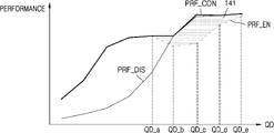
도 14를 참조하면, 가로축은 QD를 나타내고, 세로축은 성능을 나타낸다. 도 14에서는, 프리페치 인에이블(PRF_EN) 시 독출 성능, 프리페치 디스에이블(PRF_DIS) 시 독출 성능, 및 본 실시예에 따른 프리페치 제어(PRF_CON) 시 독출 성능이 예시되었다. 제1 QD(QD_a) 내지 제5 QD(QD_e)는 서로 다른 임의의 QD들에 대응할 수 있다. 이하에서는, 도 3, 도 6 및 도 14를 함께 참조하여 설명하기로 한다.Referring to FIG. 14 , the horizontal axis represents QD, and the vertical axis represents performance. In FIG. 14 , read performance when prefetch is enabled (PRF_EN), read performance when prefetch is disabled (PRF_DIS), and read performance when prefetch is controlled (PRF_CON) according to the present embodiment are exemplified. The first QDs (QD_a) to the fifth QDs (QD_e) may correspond to different random QDs. Hereinafter, it will be described with reference to FIGS. 3, 6 and 14 together.
비휘발성 메모리(220)에 대한 시퀀셜 독출 동작이 수행되는 경우, 제1 QD(QD_a)까지는 프리페치 인에이블(PRF_EN) 시 독출 성능이 프리페치 디스에이블(PRF_DIS) 시 독출 성능 보다 높을 수 있다. 그러나, QD가 제1 QD(QD_a) 보다 높아질 경우, 프리페치 디스에이블(PRF_DIS) 시 독출 성능이 프리페치 인에이블(PRF_EN) 시 독출 성능 보다 높아질 수 있다.When a sequential read operation on the
본 실시예에 따르면, 스토리지 장치(200)의 프리페치 제어 회로(211)는 프리페치 제어(PRF_CON)를 통해, 프리페치 인에이블(PRF_EN) 시의 독출 성능에 비해 성능 개선 구간(141)만큼 독출 성능을 향상시킬 수 있다. 프리페치 제어 회로(211)는 시퀀셜 독출 동작 시, 프리페치 요청 신호(REQ_PRF)를 인에이블 레벨로 생성하는 인에이블 모드를 디폴트 모드로 결정하고, 프리페치 요청 신호(REQ_PRF)를 주기적으로 디스에이블 레벨로 생성하고 독출 성능을 체크하여 프리페치 모드를 프리페치 인에이블 모드 또는 디스에이블 모드로 동적으로 결정할 수 있다. 이에 따라, QD가 제1 QD(QD_a) 보다 높은 경우에도, 프리페치 요청 신호(REQ_PRF)를 동적으로 제어함으로써 독출 성능을 전반적으로 향상시킬 수 있다.According to the present embodiment, the
도 15는 본 발명의 일 실시예에 따른 스토리지 장치가 적용된 시스템(1000)을 도시한 도면이다. 도 15의 시스템(1000)은 기본적으로 휴대용 통신 단말기(mobile phone), 스마트폰(smart phone), 태블릿 PC(tablet personal computer), 웨어러블 기기, 헬스케어 기기 또는 IOT(internet of things) 기기와 같은 모바일(mobile) 시스템일 수 있다. 하지만 도 15의 시스템(1000)은 반드시 모바일 시스템에 한정되는 것은 아니고, 개인용 컴퓨터(personal computer), 랩탑(laptop) 컴퓨터, 서버(server), 미디어 재생기(media player) 또는 내비게이션(navigation)과 같은 차량용 장비(automotive device) 등이 될 수도 있다.15 is a diagram illustrating a
도 15를 참조하면, 시스템(1000)은 메인 프로세서(main processor)(1100), 메모리(1200a, 1200b) 및 스토리지 장치(1300a, 1300b)를 포함할 수 있으며, 추가로 촬영 장치(image capturing device)(1410), 사용자 입력 장치(user input device)(1420), 센서(1430), 통신 장치(1440), 디스플레이(1450), 스피커(1460), 전력 공급 장치(power supplying device)(1470) 및 연결 인터페이스(connecting interface)(1480) 중 하나 이상을 포함할 수 있다.Referring to FIG. 15 , a
메인 프로세서(1100)는 시스템(1000)의 전반적인 동작, 보다 구체적으로는 시스템(1000)을 이루는 다른 구성 요소들의 동작을 제어할 수 있다. 이와 같은 메인 프로세서(1100)는 범용 프로세서, 전용 프로세서 또는 애플리케이션 프로세서(application processor) 등으로 구현될 수 있다. The
메인 프로세서(1100)는 하나 이상의 CPU 코어(1110)를 포함할 수 있으며, 메모리(1200a, 1200b) 및/또는 스토리지 장치(1300a, 1300b)를 제어하기 위한 컨트롤러(1120)를 더 포함할 수 있다. 실시예에 따라서는, 메인 프로세서(1100)는 AI(artificial intelligence) 데이터 연산 등 고속 데이터 연산을 위한 전용 회로인 가속기(accelerator)(1130)를 더 포함할 수 있다. 이와 같은 가속기(1130)는 GPU(Graphics Processing Unit), NPU(Neural Processing Unit) 및/또는 DPU(Data Processing Unit) 등을 포함할 수 있으며, 메인 프로세서(1100)의 다른 구성 요소와는 물리적으로 독립된 별개의 칩(chip)으로 구현될 수도 있다.The
메모리(1200a, 1200b)는 시스템(1000)의 주기억 장치로 사용될 수 있으며, SRAM 및/또는 DRAM 등의 휘발성 메모리를 포함할 수 있으나, 플래시 메모리, PRAM 및/또는 RRAM 등의 비휘발성 메모리를 포함할 수도 있다. 메모리(1200a, 1200b)는 메인 프로세서(1100)와 동일한 패키지 내에 구현되는 것도 가능하다.The
스토리지 장치(1300a, 1300b)는 전원 공급 여부와 관계 없이 데이터를 저장하는 비휘발성 저장 장치로서 기능할 수 있으며, 메모리(1200a, 1200b)에 비해 상대적으로 큰 저장 용량을 가질 수 있다. 스토리지 장치(1300a, 1300b)는 스토리지 컨트롤러(1310a, 1310b)와, 스토리지 컨트롤러(1310a, 1310b)의 제어 하에 데이터를 저장하는 비휘발성 메모리(non-volatile memory, NVM)(1320a, 1320b)를 포함할 수 있다. 비휘발성 메모리(1320a, 1320b)는 2D(2-dimensional) 구조 혹은 3D(3-dimensional) V-NAND(Vertical NAND) 구조의 플래시 메모리를 포함할 수 있으나, PRAM 및/또는 RRAM 등의 다른 종류의 비휘발성 메모리를 포함할 수도 있다. The
스토리지 장치(1300a, 1300b)는 메인 프로세서(1100)와는 물리적으로 분리된 상태로 시스템(1000)에 포함될 수도 있고, 메인 프로세서(1100)와 동일한 패키지 내에 구현될 수도 있다. 또한, 스토리지 장치(1300a, 1300b)는 SSD(solid state device) 혹은 메모리 카드(memory card)와 같은 형태를 가짐으로써, 후술할 연결 인터페이스(1480)와 같은 인터페이스를 통해 시스템(1000)의 다른 구성 요소들과 탈부착 가능하도록 결합될 수도 있다. 이와 같은 스토리지 장치(1300a, 1300b)는 UFS(Universal Flash Storage), eMMC(embedded multi-media card) 혹은 NVMe(non-volatile memory express)와 같은 표준 규약이 적용되는 장치일 수 있으나, 반드시 이에 한정되는 건 아니다.The
촬영 장치(1410)는 정지 영상 또는 동영상을 촬영할 수 있으며, 카메라(camera), 캠코더(camcorder) 및/또는 웹캠(webcam) 등일 수 있다. 사용자 입력 장치(1420)는 시스템(1000)의 사용자로부터 입력된 다양한 유형의 데이터를 수신할 수 있으며, 터치 패드(touch pad), 키패드(keypad), 키보드(keyboard), 마우스(mouse) 및/또는 마이크(microphone) 등일 수 있다. 센서(1430)는 시스템(1000)의 외부로부터 획득될 수 있는 다양한 유형의 물리량을 감지하고, 감지된 물리량을 전기 신호로 변환할 수 있다. 이와 같은 센서(1430)는 온도 센서, 압력 센서, 조도 센서, 위치 센서, 가속도 센서, 바이오 센서(biosensor) 및/또는 자이로스코프(gyroscope) 센서 등일 수 있다. 통신 장치(1440)는 다양한 통신 규약에 따라 시스템(1000) 외부의 다른 장치들과의 사이에서 신호의 송신 및 수신을 수행할 수 있다. 이와 같은 통신 장치(1440)는 안테나, 트랜시버(transceiver) 및/또는 모뎀(MODEM) 등을 포함하여 구현될 수 있다. The photographing
디스플레이(1450) 및 스피커(1460)는 시스템(1000)의 사용자에게 각각 시각적 정보와 청각적 정보를 출력하는 출력 장치로 기능할 수 있다. 전력 공급 장치(1470)는 시스템(1000)에 내장된 배터리(도시 안함) 및/또는외부 전원으로부터 공급되는 전력을 적절히 변환하여 시스템(1000)의 각 구성 요소들에게 공급할 수 있다. 연결 인터페이스(1480)는 시스템(1000)과, 시스템(1000)에 연결되어 시스템(1000과 데이터를 주고받을 수 있는 외부 장치 사이의 연결을 제공할 수 있다. 연결 인터페이스(1480)는 ATA(Advanced Technology Attachment), SATA(Serial ATA), e-SATA(external SATA), SCSI(Small Computer Small Interface), SAS(Serial Attached SCSI), PCI(Peripheral Component Interconnection), PCIe(PCI express), NVMe, IEEE 1394, USB(universal serial bus), SD(secure digital) 카드, MMC(multi-media card), eMMC, UFS, eUFS(embedded Universal Flash Storage), CF(compact flash) 카드 인터페이스 등과 같은 다양한 인터페이스 방식으로 구현될 수 있다.The
도 16은 본 발명의 예시적인 실시예에 따른 호스트-스토리지 시스템(2000)을 나타내는 블록도이다. 호스트-스토리지 시스템(2000)은 호스트(2100) 및 스토리지 장치(2200)를 포함할 수 있다. 또한, 스토리지 장치(2200)는 스토리지 컨트롤러(2210) 및 비휘발성 메모리(NVM)(2220)를 포함할 수 있다. 또한, 본 발명의 예시적인 실시예에 따라, 호스트(2100)는 호스트 컨트롤러(2110) 및 호스트 메모리(2120)를 포함할 수 있다. 호스트 메모리(2120)는 스토리지 장치(2200)로 전송될 데이터, 혹은 스토리지 장치(2200)로부터 전송된 데이터를 임시로 저장하기 위한 버퍼 메모리로서 기능할 수 있다. 예를 들어, 비휘발성 메모리(2220)는 도 1의 비휘발성 메모리(220)에 대응할 수 있고, 스토리지 컨트롤러(2210)는 도 1의 스토리지 컨트롤러(210)에 대응할 수 있고, 호스트(2100)는 도 1의 호스트(100)에 대응할 수 있다.16 is a block diagram illustrating a host-
스토리지 장치(2200)는 호스트(2100)로부터의 요청에 따라 데이터를 저장하기 위한 저장 매체들을 포함할 수 있다. 일 예로서, 스토리지 장치(2200)는 SSD(Solid State Drive), 임베디드(embedded) 메모리 및 착탈 가능한 외장(external) 메모리 중 적어도 하나를 포함할 수 있다. 스토리지 장치(2200)가 SSD인 경우, 스토리지 장치(2200)는 NVMe(non-volatile memory express) 표준을 따르는 장치일 수 있다. 스토리지 장치(2200)가 임베디드 메모리 혹은 외장(external) 메모리인 경우, 스토리지 장치(2200)는 UFS(universal flash storage) 혹은 eMMC(embedded multi-media card) 표준을 따르는 장치일 수 있다. 호스트(2100)와 스토리지 장치(2200)는 각각 채용된 표준 프로토콜에 따른 패킷을 생성하고 이를 전송할 수 있다.The
스토리지 장치(2200)의 비휘발성 메모리(2220)가 플래시 메모리를 포함할 때, 상기 플래시 메모리는 2D NAND 메모리 어레이나 3D(또는 수직형, Vertical) NAND(VNAND) 메모리 어레이를 포함할 수 있다. 다른 예로서, 스토리지 장치(2200)는 다른 다양한 종류의 비휘발성 메모리들을 포함할 수도 있다. 예를 들어, 스토리지 장치(2200)는 MRAM(Magnetic RAM), 스핀전달토크 MRAM(Spin-Transfer Torgue MRAM), Conductive bridging RAM(CBRAM), FeRAM(Ferroelectric RAM), PRAM(Phase RAM), 저항 메모리(Resistive RAM) 및 다른 다양한 종류의 메모리가 적용될 수 있다.When the
일 실시예에 따라, 호스트 컨트롤러(2110)와 호스트 메모리(2120)는 별도의 반도체 칩으로 구현될 수 있다. 또는, 일부 실시예들에서, 호스트 컨트롤러(2110)와 호스트 메모리(2120)는 동일한 반도체 칩에 집적될 수 있다. 일 예로서, 호스트 컨트롤러(2110)는 애플리케이션 프로세서(Application Processor)에 구비되는 다수의 모듈들 중 어느 하나일 수 있으며, 상기 애플리케이션 프로세서는 시스템 온 칩(System on Chip, SoC)으로 구현될 수 있다. 또한, 호스트 메모리(2120)는 상기 애플리케이션 프로세서 내에 구비되는 임베디드 메모리이거나, 또는 상기 애플리케이션 프로세서의 외부에 배치되는 비휘발성 메모리 또는 메모리 모듈일 수 있다.According to an embodiment, the
호스트 컨트롤러(2110)는 호스트 메모리(2120)의 버퍼 영역의 데이터(예컨대, 기록 데이터)를 비휘발성 메모리(2220)에 저장하거나, 비휘발성 메모리(2220)의 데이터(예컨대, 독출 데이터)를 버퍼 영역에 저장하는 동작을 관리할 수 있다.The
스토리지 컨트롤러(2210)는 호스트 인터페이스(2211), 메모리 인터페이스(2212) 및 CPU(central processing unit)(2213)를 포함할 수 있다. 또한, 스토리지 컨트롤러(2210)는 플래시 변환 레이어(Flash Translation Layer; FTL)(2214), 패킷 매니저(2215), 버퍼 메모리(2216), ECC(error correction code)(2217) 엔진 및 AES(advanced encryption standard) 엔진(2218)을 더 포함할 수 있다. 스토리지 컨트롤러(2210)는 플래시 변환 레이어(FTL)(2214)가 로딩되는 워킹 메모리(미도시)를 더 포함할 수 있으며, CPU(2213)가 플래시 변환 레이어를 실행하는 것에 의해 비휘발성 메모리(2220)에 대한 데이터 기록 및 독출 동작이 제어될 수 있다.The
호스트 인터페이스(2211)는 호스트(2100)와 패킷(packet)을 송수신할 수 있다. 호스트(2100)로부터 호스트 인터페이스(2211)로 전송되는 패킷은 커맨드(command) 혹은 비휘발성 메모리(2220)에 기록될 데이터 등을 포함할 수 있으며, 호스트 인터페이스(2211)로부터 호스트(2100)로 전송되는 패킷은 커맨드에 대한 응답(response) 혹은 비휘발성 메모리(2220)로부터 독출된 데이터 등을 포함할 수 있다. 메모리 인터페이스(2212)는 비휘발성 메모리(2220)에 기록될 데이터를 비휘발성 메모리(2220)로 송신하거나, 비휘발성 메모리(2220)로부터 독출된 데이터를 수신할 수 있다. 이러한 메모리 인터페이스(2212)는 토글(Toggle) 혹은 온파이(Open NAND Flash Interface; ONFI)와 같은 표준 규약을 준수하도록 구현될 수 있다.The
플래시 변환 계층(2214)은 어드레스 매핑(address mapping), 웨어-레벨링(wear-leveling), 가비지 콜렉션(garbage collection)과 같은 여러 기능을 수행할 수 있다. 어드레스 매핑 동작은 호스트(2100)로부터 수신한 논리 어드레스(logical address)를, 비휘발성 메모리(2220) 내에 데이터를 실제로 저장하는 데 사용되는 물리 어드레스(physical address)로 바꾸는 동작이다. 웨어-레벨링은 비휘발성 메모리(2220) 내의 블록(block)들이 균일하게 사용되도록 하여 특정 블록의 과도한 열화를 방지하기 위한 기술로, 예시적으로 물리 블록(physical block)들의 소거 카운트들을 밸런싱하는 펌웨어 기술을 통해 구현될 수 있다. 가비지 콜렉션은, 블록의 유효 데이터를 새 블록에 복사한 후 기존 블록을 소거(erase)하는 방식을 통해 비휘발성 메모리(2220) 내에서 사용 가능한 용량을 확보하기 위한 기술이다.The
패킷 매니저(2215)는 호스트(2100)와 협의된 인터페이스의 프로토콜에 따른 패킷(Packet)을 생성하거나, 호스트(2100)로부터 수신된 패킷(Packet)으로부터 각종 정보를 파싱할 수 있다. 또한, 버퍼 메모리(2216)는 비휘발성 메모리(2220)에 기록될 데이터 혹은 비휘발성 메모리(2220)로부터 독출될 데이터를 임시로 저장할 수 있다. 버퍼 메모리(2216)는 스토리지 컨트롤러(2210) 내에 구비되는 구성일 수 있으나, 스토리지 컨트롤러(2210)의 외부에 배치되어도 무방하다.The
ECC 엔진(2217)은 비휘발성 메모리(2220)로부터 독출되는 독출 데이터에 대한 오류 검출 및 정정 기능을 수행할 수 있다. 보다 구체적으로, ECC 엔진(2217)은 비휘발성 메모리(2220)에 기입될 기입 데이터에 대하여 패리티 비트(parity bit)들을 생성할 수 있으며, 이와 같이 생성된 패리티 비트들은 기입 데이터와 함께 비휘발성 메모리(2220) 내에 저장될 수 있다. 비휘발성 메모리(2220)로부터의 데이터 독출 시, ECC 엔진(2217)은 독출 데이터와 함께 비휘발성 메모리(2220)로부터 독출되는 패리티 비트들을 이용하여 독출 데이터의 에러를 정정하고, 에러가 정정된 독출 데이터를 출력할 수 있다.The
AES 엔진(2218)은, 스토리지 컨트롤러(2210)로 입력되는 데이터에 대한 암호화(encryption) 동작과 복호화(decryption) 동작 중 적어도 하나를, 대칭 키 알고리즘(symmetric-key algorithm)를 이용하여 수행할 수 있다.The
도 17은 본 개시의 일 실시예에 따른 메모리 시스템(3000)을 나타내는 블록도이다. 17 is a block diagram illustrating a
도 17을 참조하면, 메모리 시스템(3000)은 메모리 장치(3200) 및 메모리 컨트롤러(3100)를 포함할 수 있다. 메모리 장치(3200)는 복수의 채널들 중 하나를 기반으로 메모리 컨트롤러(3100)와 통신하는 비휘발성 메모리 장치들 중 하나에 대응할 수 있다. 예를 들어, 메모리 장치(3200)는 도 3의 비휘발성 메모리(220)에 대응할 수 있고, 메모리 컨트롤러(3100)는 도 3의 스토리지 컨트롤러(210)에 대응할 수 있다.Referring to FIG. 17 , the
메모리 장치(3200)는 제1 내지 제8 핀들(P11~P18), 메모리 인터페이스 회로(3210), 제어 로직 회로(3220), 및 메모리 셀 어레이(3230)를 포함할 수 있다. 메모리 인터페이스 회로(3210)는 제1 핀(P11)을 통해 메모리 컨트롤러(3100)로부터 칩 인에이블 신호(nCE)를 수신할 수 있다. 메모리 인터페이스 회로(3210)는 칩 인에이블 신호(nCE)에 따라 제2 내지 제8 핀들(P12~P18)을 통해 메모리 컨트롤러(3100)와 신호들을 송수신할 수 있다. 예를 들어, 칩 인에이블 신호(nCE)가 인에이블 상태(예를 들어, 로우 레벨)인 경우, 메모리 인터페이스 회로(3310)는 제2 내지 제8 핀들(P12~P18)을 통해 메모리 컨트롤러(3100)와 신호들을 송수신할 수 있다. The
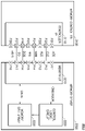
메모리 인터페이스 회로(3210)는 제2 내지 제4 핀들(P12~P14)을 통해 메모리 컨트롤러(3100)로부터 커맨드 래치 인에이블 신호(CLE), 어드레스 래치 인에이블 신호(ALE), 및 쓰기 인에이블 신호(nWE)를 수신할 수 있다. 메모리 인터페이스 회로(3210)는 제7 핀(P17)을 통해 메모리 컨트롤러(3100)로부터 데이터 신호(DQ)를 수신하거나, 메모리 컨트롤러(3100)로 데이터 신호(DQ)를 전송할 수 있다. 데이터 신호(DQ)를 통해 커맨드(CMD), 어드레스(ADDR), 및 데이터(DATA)가 전달될 수 있다. 예를 들어, 데이터 신호(DQ)는 복수의 데이터 신호 라인들을 통해 전달될 수 있다. 이 경우, 제7 핀(P17)은 복수의 데이터 신호들에 대응하는 복수개의 핀들을 포함할 수 있다.The
메모리 인터페이스 회로(3210)는 쓰기 인에이블 신호(nWE)의 토글 타이밍들에 기초하여 커맨드 래치 인에이블 신호(CLE)의 인에이블 구간(예를 들어, 하이 레벨 상태)에서 수신되는 데이터 신호(DQ)로부터 커맨드(CMD)를 획득할 수 있다. 메모리 인터페이스 회로(3210)는 쓰기 인에이블 신호(nWE)의 토글 타이밍들에 기초하여 어드레스 래치 인에이블 신호(ALE)의 인에이블 구간(예를 들어, 하이 레벨 상태)에서 수신되는 데이터 신호(DQ)로부터 어드레스(ADDR)를 획득할 수 있다.The
예시적인 실시 예에서, 쓰기 인에이블 신호(nWE)는 고정된(static) 상태(예를 들어, 하이(high) 레벨 또는 로우(low) 레벨)를 유지하다가 하이 레벨과 로우 레벨 사이에서 토글할 수 있다. 예를 들어, 쓰기 인에이블 신호(nWE)는 커맨드(CMD) 또는 어드레스(ADDR)가 전송되는 구간에서 토글할 수 있다. 이에 따라, 메모리 인터페이스 회로(3210)는 쓰기 인에이블 신호(nWE)의 토글 타이밍들에 기초하여 커맨드(CMD) 또는 어드레스(ADDR)를 획득할 수 있다.In an exemplary embodiment, the write enable signal nWE may be toggled between a high level and a low level while maintaining a static state (eg, a high level or a low level). have. For example, the write enable signal nWE may be toggled in a period in which the command CMD or the address ADDR is transmitted. Accordingly, the
메모리 인터페이스 회로(3210)는 제5 핀(P15)을 통해 메모리 컨트롤러(3100)로부터 읽기 인에이블 신호(nRE)를 수신할 수 있다. 메모리 인터페이스 회로(3210)는 제6 핀(P16)을 통해 메모리 컨트롤러(3100)로부터 데이터 스트로브 신호(DQS)를 수신하거나, 메모리 컨트롤러(3100)로 데이터 스트로브 신호(DQS)를 전송할 수 있다.The
메모리 장치(3200)의 데이터(DATA) 출력 동작에서, 메모리 인터페이스 회로(3210)는 데이터(DATA)를 출력하기 전에 제5 핀(P15)을 통해 토글하는 읽기 인에이블 신호(nRE)를 수신할 수 있다. 메모리 인터페이스 회로(3210)는 읽기 인에이블 신호(nRE)의 토글링에 기초하여 토글하는 데이터 스트로브 신호(DQS)를 생성할 수 있다. 예를 들어, 메모리 인터페이스 회로(3210)는 읽기 인에이블 신호(nRE)의 토글링 시작 시간을 기준으로 미리 정해진 딜레이(예를 들어, tDQSRE) 이후에 토글하기 시작하는 데이터 스트로브 신호(DQS)를 생성할 수 있다. 메모리 인터페이스 회로(310)는 데이터 스트로브 신호(DQS)의 토글 타이밍에 기초하여 데이터(DATA)를 포함하는 데이터 신호(DQ)를 전송할 수 있다. 이에 따라, 데이터(DATA)는 데이터 스트로브 신호(DQS)의 토글 타이밍에 정렬되어 메모리 컨트롤러(3100)로 전송될 수 있다.In the data output operation of the
메모리 장치(3200)의 데이터(DATA) 입력 동작에서, 메모리 컨트롤러(3100)로부터 데이터(DATA)를 포함하는 데이터 신호(DQ)이 수신되는 경우, 메모리 인터페이스 회로(3210)는 메모리 컨트롤러(3100)로부터 데이터(DATA)와 함께 토글하는 데이터 스트로브 신호(DQS)를 수신할 수 있다. 메모리 인터페이스 회로(3210)는 데이터 스트로브 신호(DQS)의 토글 타이밍에 기초하여 데이터 신호(DQ)로부터 데이터(DATA)를 획득할 수 있다. 예를 들어, 메모리 인터페이스 회로(3210)는 데이터 스트로브 신호(DQS)의 상승 에지 및 하강 에지에서 데이터 신호(DQ)를 샘플링함으로써 데이터(DATA)를 획득할 수 있다.In the data input operation of the
메모리 인터페이스 회로(3210)는 제8 핀(P18)을 통해 레디/비지 출력 신호(nR/B)를 메모리 컨트롤러(3100)로 전송할 수 있다. 메모리 인터페이스 회로(3210)는 레디/비지 출력 신호(nR/B)를 통해 메모리 장치(3200)의 상태 정보를 메모리 컨트롤러(3100)로 전송할 수 있다. 메모리 장치(3200)가 비지 상태인 경우(즉, 메모리 장치(3200) 내부 동작들이 수행 중인 경우), 메모리 인터페이스 회로(3210)는 비지 상태를 나타내는 레디/비지 출력 신호(nR/B)를 메모리 컨트롤러(3100)로 전송할 수 있다. 메모리 장치(3200)가 레디 상태인 경우(즉, 메모리 장치(3200) 내부 동작들이 수행되지 않거나 완료된 경우), 메모리 인터페이스 회로(3210)는 레디 상태를 나타내는 레디/비지 출력 신호(nR/B)를 메모리 컨트롤러(3100)로 전송할 수 있다. 예를 들어, 메모리 장치(3200)가 페이지 독출 명령에 응답하여 메모리 셀 어레이(3230)로부터 데이터(DATA)를 독출하는 동안, 메모리 인터페이스 회로(3210)는 비지 상태(예를 들어, 로우 레벨)를 나타내는 레디/비지 출력 신호(nR/B)를 메모리 컨트롤러(3100)로 전송할 수 있다. 예를 들어, 메모리 장치(3200)가 프로그램 명령에 응답하여 메모리 셀 어레이(3230)로 데이터(DATA)를 프로그램하는 동안, 메모리 인터페이스 회로(3210)는 비지 상태를 나타내는 레디/비지 출력 신호(nR/B)를 메모리 컨트롤러(3100)로 전송할 수 있다.The
제어 로직 회로(3220)는 메모리 장치(3200)의 각종 동작을 전반적으로 제어할 수 있다. 제어 로직 회로(3220)는 메모리 인터페이스 회로(3210)로부터 획득된 커맨드/어드레스(CMD/ADDR)를 수신할 수 있다. 제어 로직 회로(3220)는 수신된 커맨드/어드레스(CMD/ADDR)에 따라 메모리 장치(3200)의 다른 구성 요소들을 제어하기 위한 제어 신호들을 생성할 수 있다. 예를 들어, 제어 로직 회로(3220)는 메모리 셀 어레이(3230)에 데이터(DATA)를 프로그램하거나, 또는 메모리 셀 어레이(3230)로부터 데이터(DATA)를 독출하기 위한 각종 제어 신호들을 생성할 수 있다.The
메모리 셀 어레이(3230)는 제어 로직 회로(3220)의 제어에 따라 메모리 인터페이스 회로(3210)로부터 획득된 데이터(DATA)를 저장할 수 있다. 메모리 셀 어레이(3230)는 제어 로직 회로(3220)의 제어에 따라 저장된 데이터(DATA)를 메모리 인터페이스 회로(3210)로 출력할 수 있다.The
메모리 셀 어레이(3230)는 복수의 메모리 셀들을 포함할 수 있다. 예를 들어, 복수의 메모리 셀들은 플래시 메모리 셀들일 수 있다. 그러나, 본 발명은 이에 한정되지 않으며, 메모리 셀들은 RRAM(Resistive Random Access Memory) 셀, FRAM(Ferroelectric Random Access Memory) 셀, PRAM(Phase Change Random Access Memory) 셀, TRAM(Thyristor Random Access Memory) 셀, MRAM(Magnetic Random Access Memory) 셀들일 수 있다. 이하에서는, 메모리 셀들이 낸드(NAND) 플래시 메모리 셀들인 실시 예를 중심으로 본 발명의 실시 예들이 설명될 것이다.The
메모리 컨트롤러(3100)는 제1 내지 제8 핀들(P21~P28), 및 컨트롤러 인터페이스 회로(3110)를 포함할 수 있다. 제1 내지 제8 핀들(P21~P28)은 메모리 장치(3200)의 제1 내지 제8 핀들(P11~P18)에 대응할 수 있다. 컨트롤러 인터페이스 회로(3110)는 제1 핀(P21)을 통해 메모리 장치(3200)로 칩 인에이블 신호(nCE)를 전송할 수 있다. 컨트롤러 인터페이스 회로(3110)는 칩 인에이블 신호(nCE)를 통해 선택한 메모리 장치(3200)와 제2 내지 제8 핀들(P22~P28)을 통해 신호들을 송수신할 수 있다.The
컨트롤러 인터페이스 회로(3110)는 제2 내지 제4 핀들(P22~P24)을 통해 커맨드 래치 인에이블 신호(CLE), 어드레스 래치 인에이블 신호(ALE), 및 쓰기 인에이블 신호(nWE)를 메모리 장치(3200)로 전송할 수 있다. 컨트롤러 인터페이스 회로(3110)는 제7 핀(P27)을 통해 메모리 장치(3200)로 데이터 신호(DQ)를 전송하거나, 메모리 장치(3200)로부터 데이터 신호(DQ)를 수신할 수 있다.The
컨트롤러 인터페이스 회로(3110)는 토글하는 쓰기 인에이블 신호(nWE)와 함께 커맨드(CMD) 또는 어드레스(ADDR)를 포함하는 데이터 신호(DQ)를 메모리 장치(3200)로 전송할 수 있다. 컨트롤러 인터페이스 회로(3110)는 인에이블 상태를 가지는 커맨드 래치 인에이블 신호(CLE)를 전송함에 따라 커맨드(CMD)를 포함하는 데이터 신호(DQ)를 메모리 장치(3200)로 전송하고, 인에이블 상태를 가지는 어드레스 래치 인에이블 신호(ALE)를 전송함에 따라 어드레스(ADDR)를 포함하는 데이터 신호(DQ)를 메모리 장치(3200)로 전송할 수 있다.The
컨트롤러 인터페이스 회로(3110)는 제5 핀(P25)을 통해 메모리 장치(3200)로 읽기 인에이블 신호(nRE)를 전송할 수 있다. 컨트롤러 인터페이스 회로(3110)는 제6 핀(P26)을 통해 메모리 장치(3200)로부터 데이터 스트로브 신호(DQS)를 수신하거나, 메모리 장치(3200)로 데이터 스트로브 신호(DQS)를 전송할 수 있다.The
메모리 장치(3200)의 데이터(DATA) 출력 동작에서, 컨트롤러 인터페이스 회로(3110)는 토글하는 읽기 인에이블 신호(nRE)를 생성하고, 읽기 인에이블 신호(nRE)를 메모리 장치(3200)로 전송할 수 있다. 예를 들어, 컨트롤러 인터페이스 회로(3110)는 데이터(DATA)가 출력되기 전에 고정된 상태(예를 들어, 하이 레벨 또는 로우 레벨)에서 토글 상태로 변경되는 읽기 인에이블 신호(nRE)를 생성할 수 있다. 이에 따라, 메모리 장치(3200)에서 읽기 인에이블 신호(nRE)에 기초하여 토글하는 데이터 스트로브 신호(DQS)가 생성될 수 있다. 컨트롤러 인터페이스 회로(3110)는 메모리 장치(3200)로부터 토글하는 데이터 스트로브 신호(DQS)와 함께 데이터(DATA)를 포함하는 데이터 신호(DQ)를 수신할 수 있다. 컨트롤러 인터페이스 회로(3110)는 데이터 스트로브 신호(DQS)의 토글 타이밍에 기초하여 데이터 신호(DQ)로부터 데이터(DATA)를 획득할 수 있다.In the data output operation of the
메모리 장치(3200)의 데이터(DATA) 입력 동작에서, 컨트롤러 인터페이스 회로(3110)는 토글하는 데이터 스트로브 신호(DQS)를 생성할 수 있다. 예를 들어, 컨트롤러 인터페이스 회로(3110)는 데이터(DATA)를 전송하기 전에 고정된 상태(예를 들어, 하이 레벨 또는 로우 레벨)에서 토글 상태로 변경되는 데이터 스트로브 신호(DQS)를 생성할 수 있다. 컨트롤러 인터페이스 회로(3110)는 데이터 스트로브 신호(DQS)의 토글 타이밍들에 기초하여 데이터(DATA)를 포함하는 데이터 신호(DQ)를 메모리 장치(3200)로 전송할 수 있다. 컨트롤러 인터페이스 회로(3110)는 제8 핀(P28)을 통해 메모리 장치(3200)로부터 레디/비지 출력 신호(nR/B)를 수신할 수 있다. 컨트롤러 인터페이스 회로(3110)는 레디/비지 출력 신호(nR/B)에 기초하여 메모리 장치(3200)의 상태 정보를 판별할 수 있다.In a data input operation of the
도 18은 본 발명의 일 실시예에 따른 메모리 장치에 적용될 수 있는 B-VNAND 구조에 대해 설명하기 위한 도면이다. 메모리 장치에 포함되는 비휘발성 메모리가 B-VNAND(Bonding Vertical NAND) 타입의 플래시 메모리로 구현될 경우, 비휘발성 메모리는 도 18에 도시된 구조를 가질 수 있다.18 is a diagram for explaining a B-VNAND structure applicable to a memory device according to an embodiment of the present invention. When the nonvolatile memory included in the memory device is implemented as a B-VNAND (Bonding Vertical NAND) type flash memory, the nonvolatile memory may have the structure shown in FIG. 18 .
도 18을 참조하면, 메모리 장치(4000)는 C2C(chip to chip) 구조일 수 있다. C2C 구조는 제1 웨이퍼 상에 셀 영역(CELL)을 포함하는 상부 칩을 제작하고, 제1 웨이퍼와 다른 제2 웨이퍼 상에 주변 회로 영역(PERI)을 포함하는 하부 칩을 제작한 후, 상기 상부 칩과 상기 하부 칩을 본딩(bonding) 방식에 의해 서로 연결하는 것을 의미할 수 있다. 일례로, 상기 본딩 방식은 상부 칩의 최상부 메탈층에 형성된 본딩 메탈과 하부 칩의 최상부 메탈층에 형성된 본딩 메탈을 서로 전기적으로 연결하는 방식을 의미할 수 있다. 예컨대, 상기 본딩 메탈이 구리(Cu)로 형성된 경우, 상기 본딩 방식은 Cu-Cu 본딩 방식일 수 있으며, 상기 본딩 메탈은 알루미늄 혹은 텅스텐으로도 형성될 수 있다.Referring to FIG. 18 , the
메모리 장치(4000)의 주변 회로 영역(PERI)과 셀 영역(CELL) 각각은 외부 패드 본딩 영역(PA), 워드 라인 본딩 영역(WLBA), 및 비트 라인 본딩 영역(BLBA)을 포함할 수 있다. 주변 회로 영역(PERI)은 제1 기판(4110), 층간 절연층(4115), 제1 기판(4110)에 형성되는 복수의 회로 소자들(4120a, 4120b, 4120c), 복수의 회로 소자들(4120a, 4120b, 4120c) 각각과 연결되는 제1 메탈층(4130a, 4130b, 4130c), 제1 메탈층(4130a, 4130b, 4130c) 상에 형성되는 제2 메탈층(4140a, 4140b, 4140c)을 포함할 수 있다. 일 실시예에서, 제1 메탈층(4130a, 4130b, 4130c)은 상대적으로 저항이 높은 텅스텐으로 형성될 수 있고, 제2 메탈층(4140a, 4140b, 4140c)은 상대적으로 저항이 낮은 구리로 형성될 수 있다.Each of the peripheral circuit area PERI and the cell area CELL of the
본 명세서에서는 제1 메탈층(4130a, 4130b, 4130c)과 제2 메탈층(4140a, 4140b, 4140c)만 도시 되고 설명되나, 이에 한정되는 것은 아니고, 제2 메탈층(4140a, 4140b, 4140c) 상에 적어도 하나 이상의 메탈층이 더 형성될 수도 있다. 제2 메탈층(4140a, 4140b, 4140c)의 상부에 형성되는 하나 이상의 메탈층 중 적어도 일부는, 제2 메탈층(4140a, 4140b, 4140c)을 형성하는 구리보다 더 낮은 저항을 갖는 알루미늄 등으로 형성될 수 있다. 층간 절연층(4115)은 복수의 회로 소자들(4120a, 4120b, 4120c), 제1 메탈층(4130a, 4130b, 4130c), 및 제2 메탈층(4140a, 4140b, 4140c)을 커버하도록 제1 기판(4110) 상에 배치되며, 실리콘 산화물, 실리콘 질화물 등과 같은 절연 물질을 포함할 수 있다.In the present specification, only the
워드 라인 본딩 영역(WLBA)의 제2 메탈층(4140b) 상에 하부 본딩 메탈(4171b, 4172b)이 형성될 수 있다. 워드 라인 본딩 영역(WLBA)에서, 주변 회로 영역(PERI)의 하부 본딩 메탈(4171b, 4172b)은 셀 영역(CELL)의 상부 본딩 메탈(4271b, 4272b)과 본딩 방식에 의해 서로 전기적으로 연결될 수 있으며, 하부 본딩 메탈(4171b, 4172b)과 상부 본딩 메탈(4271b, 4272b)은 알루미늄, 구리, 혹은 텅스텐 등으로 형성될 수 있다.
셀 영역(CELL)은 적어도 하나의 메모리 블록을 제공할 수 있다. 셀 영역(CELL)은 제2 기판(4210)과 공통 소스 라인(4220)을 포함할 수 있다. 제2 기판(4210) 상에는, 제2 기판(4210)의 상면에 수직하는 방향(Z축 방향)을 따라 복수의 워드 라인들(4231-4238; 4230)이 적층될 수 있다. 워드 라인들(4230)의 상부 및 하부 각각에는 스트링 선택 라인들과 접지 선택 라인이 배치될 수 있으며, 스트링 선택 라인들과 접지 선택 라인 사이에 복수의 워드 라인들(4230)이 배치될 수 있다.The cell region CELL may provide at least one memory block. The cell region CELL may include a
비트 라인 본딩 영역(BLBA)에서, 채널 구조체(CH)는 제2 기판(4210)의 상면에 수직하는 방향으로 연장되어 워드 라인들(4230), 스트링 선택 라인들, 및 접지 선택 라인을 관통할 수 있다. 채널 구조체(CH)는 데이터 저장층, 채널층, 및 매립 절연층 등을 포함할 수 있으며, 채널층은 제1 메탈층(4250c) 및 제2 메탈층(4260c)과 전기적으로 연결될 수 있다. 예컨대, 제1 메탈층(4250c)은 비트 라인 컨택일 수 있고, 제2 메탈층(4260c)은 비트 라인일 수 있다. 일 실시예에서, 비트 라인(4260c)은 제2 기판(4210)의 상면에 평행한 제1 방향(Y축 방향)을 따라 연장될 수 있다. In the bit line bonding area BLBA, the channel structure CH may extend in a direction perpendicular to the top surface of the
도 18에 도시한 일 실시예에서, 채널 구조체(CH)와 비트 라인(4260c) 등이 배치되는 영역이 비트 라인 본딩 영역(BLBA)으로 정의될 수 있다. 비트 라인(4260c)은 비트 라인 본딩 영역(BLBA)에서 주변 회로 영역(PERI)에서 페이지 버퍼(4293)를 제공하는 회로 소자들(4120c)과 전기적으로 연결될 수 있다. 일례로, 비트 라인(4260c)은 주변 회로 영역(PERI)에서 상부 본딩 메탈(4271c, 4272c)과 연결되며, 상부 본딩 메탈(4271c, 4272c)은 페이지 버퍼(4293)의 회로 소자들(4120c)에 연결되는 하부 본딩 메탈(4171c, 4172c)과 연결될 수 있다.18 , an area in which the channel structure CH and the
워드 라인 본딩 영역(WLBA)에서, 워드 라인들(4230)은 제2 기판(4210)의 상면에 평행한 제2 방향(X축 방향)을 따라 연장될 수 있으며, 복수의 셀 컨택 플러그들(4241-4247; 4240)와 연결될 수 있다. 워드 라인들(4230)과 셀 컨택 플러그들(4240)은, 제2 방향을 따라 워드 라인들(4230) 중 적어도 일부가 서로 다른 길이로 연장되어 제공하는 패드들에서 서로 연결될 수 있다. 워드 라인들(4230)에 연결되는 셀 컨택 플러그들(4240)의 상부에는 제1 메탈층(4250b)과 제2 메탈층(4260b)이 차례로 연결될 수 있다. 셀 컨택 플러그들(4240)은 워드 라인 본딩 영역(WLBA)에서 셀 영역(CELL)의 상부 본딩 메탈(4271b, 4272b)과 주변 회로 영역(PERI)의 하부 본딩 메탈(4171b, 4172b)을 통해 주변 회로 영역(PERI)과 연결될 수 있다. In the word line bonding area WLBA, the
셀 컨택 플러그들(4240)은 주변 회로 영역(PERI)에서 로우 디코더(4294)를 제공하는 회로 소자들(4120b)과 전기적으로 연결될 수 있다. 일 실시예에서, 로우 디코더(4294)를 제공하는 회로 소자들(4120b)의 동작 전압은, 페이지 버퍼(4293)를 제공하는 회로 소자들(4120c)의 동작 전압과 다를 수 있다. 일례로, 페이지 버퍼(4293)를 제공하는 회로 소자들(4120c)의 동작 전압이 로우 디코더(4294)를 제공하는 회로 소자들(4120b)의 동작 전압보다 클 수 있다.The cell contact plugs 4240 may be electrically connected to the
외부 패드 본딩 영역(PA)에는 공통 소스 라인 컨택 플러그(4280)가 배치될 수 있다. 공통 소스 라인 컨택 플러그(4280)는 금속, 금속 화합물, 또는 폴리실리콘 등의 도전성 물질로 형성되며, 공통 소스 라인(4220)과 전기적으로 연결될 수 있다. 공통 소스 라인 컨택 플러그(4280) 상부에는 제1 메탈층(4250a)과 제2 메탈층(4260a)이 차례로 적층될 수 있다. 일례로, 공통 소스 라인 컨택 플러그(4280), 제1 메탈층(4250a), 및 제2 메탈층(4260a)이 배치되는 영역은 외부 패드 본딩 영역(PA)으로 정의될 수 있다.A common source
한편 외부 패드 본딩 영역(PA)에는 입출력 패드들(4105, 4205)이 배치될 수 있다. 도 18을 참조하면, 제1 기판(4110)의 하부에는 제1 기판(4110)의 하면을 덮는 하부 절연막(4101) 이 형성될 수 있으며, 하부 절연막(4101) 상에 제1 입출력 패드(4105)가 형성될 수 있다. 제1 입출력 패드(4105)는 제1 입출력 컨택 플러그(4103)를 통해 주변 회로 영역(PERI)에 배치되는 복수의 회로 소자들(4120a, 4120b, 4120c) 중 적어도 하나와 연결되며, 하부 절연막(4101)에 의해 제1 기판(4110)과 분리될 수 있다. 또한, 제1 입출력 컨택 플러그(4103)와 제1 기판(4110) 사이에는 측면 절연막이 배치되어 제1 입출력 컨택 플러그(4103)와 제1 기판(4110)을 전기적으로 분리할 수 있다.Meanwhile, input/
도 18을 참조하면, 제2 기판(4210)의 상부에는 제2 기판(4210)의 상면을 덮는 상부 절연막(4201)이 형성될 수 있으며, 상부 절연막(4201) 상에 제2 입출력 패드(4205)가 배치될 수 있다. 제2 입출력 패드(4205)는 제2 입출력 컨택 플러그(4203)를 통해 주변 회로 영역(PERI)에 배치되는 복수의 회로 소자들(4120a, 4120b, 4120c) 중 적어도 하나와 연결될 수 있다. Referring to FIG. 18 , an upper insulating
실시예들에 따라, 제2 입출력 컨택 플러그(4203)가 배치되는 영역에는 제2 기판(4210) 및 공통 소스 라인(4220) 등이 배치되지 않을 수 있다. 또한, 제2 입출력 패드(4205)는 제3 방향(Z축 방향)에서 워드 라인들(4230)과 오버랩되지 않을 수 있다. 도 18을 참조하면, 제2 입출력 컨택 플러그(4203)는 제2 기판(4210)의 상면에 평행한 방향에서 제2 기판(4210)과 분리되며, 셀 영역(CELL)의 층간 절연층(4215)을 관통하여 제2 입출력 패드(4205)에 연결될 수 있다. In some embodiments, the
실시예들에 따라, 제1 입출력 패드(4105)와 제2 입출력 패드(4205)는 선택적으로 형성될 수 있다. 일례로, 메모리 장치(4000)는 제1 기판(4110)의 상부에 배치되는 제1 입출력 패드(4105)만을 포함하거나, 또는 제2 기판(4210)의 상부에 배치되는 제2 입출력 패드(4205)만을 포함할 수 있다. 또는, 메모리 장치(4000)가 제1 입출력 패드(4105)와 제2 입출력 패드(4205)를 모두 포함할 수도 있다.In some embodiments, the first input/
셀 영역(CELL)과 주변 회로 영역(PERI) 각각에 포함되는 외부 패드 본딩 영역(PA)과 비트 라인 본딩 영역(BLBA) 각각에는 최상부 메탈층의 메탈 패턴이 더미 패턴(dummy pattern)으로 존재하거나, 최상부 메탈층이 비어있을 수 있다.In each of the external pad bonding area PA and the bit line bonding area BLBA included in the cell area CELL and the peripheral circuit area PERI, the metal pattern of the uppermost metal layer exists as a dummy pattern, or The uppermost metal layer may be empty.
메모리 장치(4000)는 외부 패드 본딩 영역(PA)에서, 셀 영역(CELL)의 최상부 메탈층에 형성된 상부 메탈 패턴(4272a)에 대응하여 주변 회로 영역(PERI)의 최상부 메탈층에 셀 영역(CELL)의 상부 메탈 패턴(4272a)과 동일한 형태의 하부 메탈 패턴(4176a)을 형성할 수 있다. 주변 회로 영역(PERI)의 최상부 메탈층에 형성된 하부 메탈 패턴(4176a)은 주변 회로 영역(PERI)에서 별도의 컨택과 연결되지 않을 수 있다. 이와 유사하게, 외부 패드 본딩 영역(PA)에서 주변 회로 영역(PERI)의 최상부 메탈층에 형성된 하부 메탈 패턴에 대응하여 셀 영역(CELL)의 상부 메탈층에 주변 회로 영역(PERI)의 하부 메탈 패턴과 동일한 형태의 상부 메탈 패턴을 형성할 수도 있다. In the external pad bonding area PA, the
워드 라인 본딩 영역(WLBA)의 제2 메탈층(4140b) 상에는 하부 본딩 메탈(4171b, 4172b)이 형성될 수 있다. 워드 라인 본딩 영역(WLBA)에서, 주변 회로 영역(PERI)의 하부 본딩 메탈(4171b, 4172b)은 셀 영역(CELL)의 상부 본딩 메탈(4271b, 4272b)과 본딩 방식에 의해 서로 전기적으로 연결될 수 있다. 또한, 비트 라인 본딩 영역(BLBA)에서, 주변 회로 영역(PERI)의 최상부 메탈층에 형성된 하부 메탈 패턴(4152)에 대응하여 셀 영역(CELL)의 최상부 메탈층에 주변 회로 영역(PERI)의 하부 메탈 패턴(4152)과 동일한 형태의 상부 메탈 패턴(4292)을 형성할 수 있다. 셀 영역(CELL)의 최상부 메탈층에 형성된 상부 메탈 패턴(4292) 상에는 컨택을 형성하지 않을 수 있다.
이상에서와 같이 도면과 명세서에서 예시적인 실시예들이 개시되었다. 본 명세서에서 특정한 용어를 사용하여 실시예들을 설명되었으나, 이는 단지 본 개시의 기술적 사상을 설명하기 위한 목적에서 사용된 것이지 의미 한정이나 특허청구범위에 기재된 본 개시의 범위를 제한하기 위하여 사용된 것은 아니다. 그러므로 본 기술분야의 통상의 지식을 가진 자라면 이로부터 다양한 변형 및 균등한 타 실시예가 가능하다는 점을 이해할 것이다. 따라서, 본 개시의 진정한 기술적 보호범위는 첨부된 특허청구범위의 기술적 사상에 의해 정해져야 할 것이다. Exemplary embodiments have been disclosed in the drawings and specification as described above. Although the embodiments have been described using specific terms in the present specification, these are used only for the purpose of explaining the technical idea of the present disclosure and not used to limit the meaning or the scope of the present disclosure described in the claims. . Therefore, it will be understood by those skilled in the art that various modifications and equivalent other embodiments are possible therefrom. Accordingly, the true technical protection scope of the present disclosure should be defined by the technical spirit of the appended claims.
Claims (20)
상기 비휘발성 메모리로부터 프리페칭된 프리페치 데이터를 버퍼링하도록 구성된 프리페치 버퍼;
상기 프리페치 데이터 또는 상기 비휘발성 메모리로부터 독출되는 노멀 데이터를 독출 데이터로서 출력하도록 구성된 판별기; 및
상기 비휘발성 메모리에 대한 시퀀셜(sequential) 독출 동작 시 프리페치 동작을 인에이블하고, 제1 시점에서 상기 프리페치 동작을 디스에이블하며, 상기 프리페치 동작이 디스에이블된 프리페치 서스펜드(suspend) 구간에서 상기 독출 데이터의 성능에 따라 상기 프리페치 동작을 인에이블 또는 디스에이블하는 프리페치 제어 회로를 포함하는 스토리지 컨트롤러.A storage controller configured to control non-volatile memory, comprising:
a prefetch buffer configured to buffer prefetch data prefetched from the non-volatile memory;
a discriminator configured to output the prefetch data or normal data read from the nonvolatile memory as read data; and
Enables a prefetch operation during a sequential read operation for the nonvolatile memory, disables the prefetch operation at a first time point, and in a prefetch suspend period in which the prefetch operation is disabled and a prefetch control circuit configured to enable or disable the prefetch operation according to performance of the read data.
호스트로부터 수신되는 시퀀셜 독출 커맨드의 어드레스가 상기 프리페치 버퍼에 버퍼링된 상기 프리페치 데이터의 어드레스에 대응하면, 상기 프리페치 데이터를 상기 독출 데이터로서 출력하는 특징으로 하는 스토리지 컨트롤러.According to claim 1, wherein the discriminator,
and outputting the prefetch data as the read data when the address of the sequential read command received from the host corresponds to the address of the prefetch data buffered in the prefetch buffer.
호스트로부터 수신되는 시퀀셜 독출 커맨드의 어드레스가 상기 프리페치 버퍼에 버퍼링된 상기 프리페치 데이터의 어드레스에 대응하지 않으면, 상기 노멀 데이터를 상기 독출 데이터로서 출력하는 특징으로 하는 스토리지 컨트롤러.According to claim 1, wherein the discriminator,
and outputting the normal data as the read data when the address of the sequential read command received from the host does not correspond to the address of the prefetch data buffered in the prefetch buffer.
호스트로부터 수신되는 연속된 독출 커맨드의 개수가 제1 기준치 보다 크면, 상기 연속된 독출 커맨드는 시퀀셜 독출 커맨드로 판단되는 것을 특징으로 하는 스토리지 컨트롤러.According to claim 1,
The storage controller of claim 1 , wherein when the number of consecutive read commands received from the host is greater than the first reference value, the consecutive read commands are determined as sequential read commands.
호스트로부터 제1 독출 커맨드 및 제1 어드레스가 수신되고, 이어서, 제2 독출 커맨드 및 제2 어드레스가 수신되는 경우, 상기 제1 및 제2 어드레스들에 따라 상기 제1 및 제2 독출 커맨드들은 시퀀셜 독출 커맨드들 또는 랜덤 독출 커맨드들로 판단되는 것을 특징으로 하는 스토리지 컨트롤러.According to claim 1,
When the first read command and the first address are received from the host, and then the second read command and the second address are received, the first and second read commands are sequentially read according to the first and second addresses. The storage controller, characterized in that it is determined as commands or random read commands.
호스트로부터 시퀀셜 독출 커맨드를 정의하는 플래그 및 독출 커맨드를 포함하는 커맨드 세트가 수신되는 경우, 상기 독출 커맨드는 시퀀셜 독출 커맨드로 판단되는 것을 특징으로 하는 스토리지 컨트롤러.According to claim 1,
The storage controller of claim 1 , wherein when a command set including a read command and a flag defining a sequential read command is received from the host, the read command is determined as a sequential read command.
상기 프리페치 제어 회로는, 상기 시퀀셜 독출 동작 시 인에이블 레벨을 갖는 프리페치 요청 신호에 따라 상기 비휘발성 메모리에 프리페치 커맨드를 전송하고,
상기 프리페치 버퍼는, 상기 프리페치 커맨드에 응답하여 상기 비휘발성 메모리가 제공하는 상기 프리페치 데이터를 버퍼링하는 것을 특징으로 하는 스토리지 컨트롤러.According to claim 1,
the prefetch control circuit transmits a prefetch command to the nonvolatile memory according to a prefetch request signal having an enable level during the sequential read operation;
The prefetch buffer is configured to buffer the prefetch data provided by the nonvolatile memory in response to the prefetch command.
상기 독출 데이터의 상기 성능을 모니터링함으로써 성능 신호를 생성하고, 생성된 상기 성능 신호를 상기 프리페치 제어 회로에 제공하는 프리페치 모니터 회로를 더 포함하는 것을 특징으로 하는 스토리지 컨트롤러.According to claim 1,
and a prefetch monitor circuit that generates a performance signal by monitoring the performance of the read data and provides the generated performance signal to the prefetch control circuit.
상기 프리페치 동작이 인에이블된 프리페치 인에이블 구간에서, 상기 성능 신호를 주기적으로 체크하거나,
상기 프리페치 서스펜드 구간에서, 상기 성능 신호를 주기적으로 체크하는 것을 특징으로 하는 스토리지 컨트롤러.9. The method of claim 8, wherein the prefetch control circuit comprises:
In the prefetch enable interval in which the prefetch operation is enabled, the performance signal is periodically checked;
The storage controller of claim 1, wherein the performance signal is periodically checked during the prefetch suspend period.
단위 시간 당 상기 스토리지 컨트롤러에서 호스트로 전달되는 상기 독출 데이터의 사이즈를 나타내는 독출 성능에 대응하는 것을 특징으로 하는 스토리지 컨트롤러.The method of claim 8, wherein the performance signal is:
The storage controller of claim 1 , wherein the storage controller corresponds to a read performance indicating a size of the read data transferred from the storage controller to the host per unit time.
상기 프리페치 서스펜드 구간에서, 상기 성능 신호가 제1 임계치 보다 크면, 프리페치 요청 신호를 디스에이블 레벨로 유지하고,
상기 프리페치 서스펜드 구간에서, 상기 성능 신호가 상기 제1 임계치 이하이면, 상기 프리페치 요청 신호를 인에이블 레벨로 변경하는 것을 특징으로 하는 스토리지 컨트롤러.9. The method of claim 8, wherein the prefetch control circuit comprises:
In the prefetch suspend period, if the performance signal is greater than a first threshold, maintaining the prefetch request signal at a disable level;
and changing the prefetch request signal to an enable level when the performance signal is equal to or less than the first threshold in the prefetch suspend period.
상기 프리페치 요청 신호가 상기 디스에이블 레벨로 유지되는 경우, 성능 체크 주기마다 상기 성능 신호를 상기 제1 임계치와 비교하고, 비교 결과에 따라 상기 프리페치 서스펜드 구간을 유지 또는 종료하는 것을 특징으로 하는 스토리지 컨트롤러.The method of claim 11 , wherein the prefetch control circuit comprises:
When the prefetch request signal is maintained at the disable level, the performance signal is compared with the first threshold every performance check period, and the prefetch suspend period is maintained or terminated according to the comparison result. controller.
상기 성능 신호가 제2 임계치 이상인 시점 이후의 시점에 대응하고,
상기 제2 임계치는 상기 제1 임계치 보다 낮은 것을 특징으로 하는 스토리지 컨트롤러.According to claim 11, wherein the first time point,
Corresponding to a time point after the point in time when the performance signal is equal to or greater than the second threshold,
wherein the second threshold is lower than the first threshold.
성능 체크 주기마다 상기 프리페치 요청 신호를 상기 디스에이블 레벨로 생성하는 것을 특징으로 하는 스토리지 컨트롤러.The method of claim 11 , wherein the prefetch control circuit comprises:
and generating the prefetch request signal at the disable level every performance check period.
상기 성능 체크 주기에 대응하는 인터벌 신호를 생성하는 인터벌 카운터를 더 포함하고,
상기 프리페치 제어 회로는,
상기 인터벌 신호에 따라 상기 프리페치 요청 신호를 상기 인에이블 레벨에서 상기 디스에이블 레벨로 변경하거나,상기 인터벌 신호에 따라 상기 성능 신호를 제1 임계치와 비교하는 것을 특징으로 하는 스토리지 컨트롤러.15. The method of claim 14,
Further comprising an interval counter for generating an interval signal corresponding to the performance check period,
The prefetch control circuit comprises:
and changing the prefetch request signal from the enable level to the disable level according to the interval signal, or comparing the performance signal with a first threshold according to the interval signal.
호스트로부터 수신된 시퀀셜 독출 커맨드를 기초로, 상기 비휘발성 메모리로부터 프리페칭된 프리페치 데이터를 프리페치 버퍼에 버퍼링하는 단계;
상기 프리페치 버퍼에 버퍼링된 상기 프리페치 데이터를 독출 데이터로서 출력하는 단계;
제1 시점에서, 상기 비휘발성 메모리로부터 독출되는 노멀 데이터를 상기 독출 데이터로서 출력하는 단계; 및
프리페치 서스펜드 구간에서, 상기 독출 데이터의 성능을 기초로 상기 프리페치 데이터 또는 상기 노멀 데이터를 상기 독출 데이터로서 출력하는 단계를 포함하는 방법.A method of operating a storage controller for controlling a non-volatile memory, comprising:
buffering the prefetch data prefetched from the nonvolatile memory in a prefetch buffer based on the sequential read command received from the host;
outputting the prefetch data buffered in the prefetch buffer as read data;
outputting normal data read from the non-volatile memory as the read data at a first time point; and
and outputting the prefetch data or the normal data as the read data based on the performance of the read data in a prefetch suspend period.
상기 프리페치 데이터를 상기 프리페치 버퍼에 버퍼링하는 단계는,
상기 호스트로부터 수신되는 연속된 독출 커맨드들의 개수가 제1 기준치 보다 크면, 상기 비휘발성 메모리에 프리페치 커맨드를 전송하는 단계; 및
상기 프리페치 커맨드에 응답하여 상기 비휘발성 메모리로부터 프리페칭된 상기 프리페치 데이터를 상기 프리페치 버퍼에 버퍼링하는 단계를 포함하는 것을 특징으로 하는 방법.17. The method of claim 16,
Buffering the prefetch data in the prefetch buffer comprises:
transmitting a prefetch command to the nonvolatile memory when the number of consecutive read commands received from the host is greater than a first reference value; and
and buffering the prefetch data prefetched from the non-volatile memory in the prefetch buffer in response to the prefetch command.
상기 프리페치 데이터를 상기 독출 데이터로서 출력하는 단계는,
호스트로부터 수신되는 시퀀셜 독출 커맨드의 어드레스가 상기 프리페치 버퍼에 버퍼링된 상기 프리페치 데이터의 어드레스에 대응하면, 상기 프리페치 데이터를 상기 독출 데이터로서 출력하는 것을 특징으로 하는 방법.17. The method of claim 16,
Outputting the prefetch data as the read data includes:
and outputting the prefetch data as the read data when the address of the sequential read command received from the host corresponds to the address of the prefetch data buffered in the prefetch buffer.
상기 프리페치 데이터 또는 상기 노멀 데이터를 상기 독출 데이터로서 출력하는 단계 이전에, 상기 독출 데이터의 상기 성능을 모니터링함으로써 성능 신호를 생성하는 단계를 더 포함하고,
상기 성능 신호는, 단위 시간 당 상기 스토리지 컨트롤러에서 호스트로 전달되는 상기 독출 데이터의 사이즈를 나타내는 독출 성능에 대응하는 것을 특징으로 하는 방법.17. The method of claim 16,
Before outputting the prefetch data or the normal data as the read data, the method further comprising: generating a performance signal by monitoring the performance of the read data;
The performance signal corresponds to a read performance indicating a size of the read data transmitted from the storage controller to the host per unit time.
호스트로부터 수신된 시퀀셜 독출 커맨드를 기초로, 상기 스토리지 컨트롤러에서 상기 비휘발성 메모리에 프리페치 커맨드를 전송하는 단계;
상기 프리페치 커맨드에 응답하여 상기 비휘발성 메모리로부터 수신된 프리페치 데이터를 프리페치 버퍼에 버퍼링하는 단계;
상기 시퀀셜 독출 커맨드를 기초로, 상기 스토리지 컨트롤러에서 상기 호스트로, 상기 프리페치 버퍼에 버퍼링된 상기 프리페치 데이터를 전달하는 단계;
제1 시간이 경과하면, 상기 스토리지 컨트롤러에서 상기 호스트로, 상기 프리페치 데이터 대신 상기 비휘발성 메모리로부터 수신되는 노멀 데이터를 전달하는 단계;
상기 노멀 데이터의 독출 성능이 제1 임계치 보다 크면, 상기 스토리지 컨트롤러에서 상기 호스트로, 상기 노멀 데이터를 전달하는 단계; 및
상기 노멀 데이터의 상기 독출 성능이 상기 제1 임계치 이하이면, 상기 스토리지 컨트롤러에서 상기 호스트로, 상기 프리페치 데이터를 전달하는 단계를 포함하는 방법.A method of operating a storage device comprising a non-volatile memory and a storage controller, the method comprising:
transmitting a prefetch command from the storage controller to the nonvolatile memory based on a sequential read command received from a host;
buffering the prefetch data received from the nonvolatile memory in a prefetch buffer in response to the prefetch command;
transferring the prefetch data buffered in the prefetch buffer from the storage controller to the host based on the sequential read command;
transferring normal data received from the nonvolatile memory instead of the prefetch data from the storage controller to the host when a first time period elapses;
transferring the normal data from the storage controller to the host when the reading performance of the normal data is greater than a first threshold; and
and transferring the prefetch data from the storage controller to the host when the read performance of the normal data is equal to or less than the first threshold.
Priority Applications (4)
| Application Number | Priority Date | Filing Date | Title |
|---|---|---|---|
| KR1020210021451A KR20220117747A (en) | 2021-02-17 | 2021-02-17 | Storage controller having data prefetching control function, operating method of storage controller, and operating method of storage device |
| US17/496,028 US11853219B2 (en) | 2021-02-17 | 2021-10-07 | Storage controller having data prefetching control function, operating method of storage controller, and operating method of storage device |
| DE102021127472.9A DE102021127472A1 (en) | 2021-02-17 | 2021-10-22 | Memory controller with a data prefetch control function, method of operation of the memory controller and method of operation of a storage device |
| CN202111372889.2A CN114942894A (en) | 2021-02-17 | 2021-11-18 | Storage controller, operation method thereof and operation method of storage device |
Applications Claiming Priority (1)
| Application Number | Priority Date | Filing Date | Title |
|---|---|---|---|
| KR1020210021451A KR20220117747A (en) | 2021-02-17 | 2021-02-17 | Storage controller having data prefetching control function, operating method of storage controller, and operating method of storage device |
Publications (1)
| Publication Number | Publication Date |
|---|---|
| KR20220117747A true KR20220117747A (en) | 2022-08-24 |
Family
ID=82610797
Family Applications (1)
| Application Number | Title | Priority Date | Filing Date |
|---|---|---|---|
| KR1020210021451A Pending KR20220117747A (en) | 2021-02-17 | 2021-02-17 | Storage controller having data prefetching control function, operating method of storage controller, and operating method of storage device |
Country Status (4)
| Country | Link |
|---|---|
| US (1) | US11853219B2 (en) |
| KR (1) | KR20220117747A (en) |
| CN (1) | CN114942894A (en) |
| DE (1) | DE102021127472A1 (en) |
Families Citing this family (7)
| Publication number | Priority date | Publication date | Assignee | Title |
|---|---|---|---|---|
| US12118236B2 (en) * | 2021-08-30 | 2024-10-15 | International Business Machines Corporation | Dynamically allocating memory controller resources for extended prefetching |
| US12197350B2 (en) | 2021-12-10 | 2025-01-14 | Samsung Electronics Co., Ltd. | Low-latency input data staging to execute kernels |
| US11989142B2 (en) * | 2021-12-10 | 2024-05-21 | Samsung Electronics Co., Ltd. | Efficient and concurrent model execution |
| US11966338B2 (en) * | 2022-07-19 | 2024-04-23 | International Business Machines Corporation | Prefetching management in database system based on number of pages being prefetched |
| KR20250058298A (en) * | 2023-10-23 | 2025-04-30 | 삼성전자주식회사 | Storage device based on flash memory and method for managing prefetch data thereof |
| US20250231880A1 (en) * | 2024-01-12 | 2025-07-17 | Arm Limited | Operational modes for prefetch generation circuitry |
| KR20260018422A (en) * | 2024-07-31 | 2026-02-09 | 에스케이하이닉스 주식회사 | Cxl stoarge device supporting speculative read operation |
Family Cites Families (24)
| Publication number | Priority date | Publication date | Assignee | Title |
|---|---|---|---|---|
| US5881254A (en) | 1996-06-28 | 1999-03-09 | Lsi Logic Corporation | Inter-bus bridge circuit with integrated memory port |
| US6381677B1 (en) * | 1998-08-19 | 2002-04-30 | International Business Machines Corporation | Method and system for staging data into cache |
| US7430641B2 (en) * | 2004-08-09 | 2008-09-30 | Xiv Ltd. | System method and circuit for retrieving into cache data from one or more mass data storage devices |
| TWI273409B (en) * | 2005-01-18 | 2007-02-11 | Sunplus Technology Co Ltd | Pre-fetch technology by read merge mechanism |
| US20060174228A1 (en) * | 2005-01-28 | 2006-08-03 | Dell Products L.P. | Adaptive pre-fetch policy |
| JP4915774B2 (en) * | 2006-03-15 | 2012-04-11 | 株式会社日立製作所 | Storage system and storage system control method |
| US7603526B2 (en) * | 2007-01-29 | 2009-10-13 | International Business Machines Corporation | Systems and methods for providing dynamic memory pre-fetch |
| US7917702B2 (en) | 2007-07-10 | 2011-03-29 | Qualcomm Incorporated | Data prefetch throttle |
| US8364901B2 (en) | 2009-02-13 | 2013-01-29 | Micron Technology, Inc. | Memory prefetch systems and methods |
| US8443151B2 (en) * | 2009-11-09 | 2013-05-14 | Intel Corporation | Prefetch optimization in shared resource multi-core systems |
| US9817761B2 (en) * | 2012-01-06 | 2017-11-14 | Sandisk Technologies Llc | Methods, systems, and computer readable media for optimization of host sequential reads or writes based on volume of data transfer |
| US9043579B2 (en) | 2012-01-10 | 2015-05-26 | International Business Machines Corporation | Prefetch optimizer measuring execution time of instruction sequence cycling through each selectable hardware prefetch depth and cycling through disabling each software prefetch instruction of an instruction sequence of interest |
| US20140108740A1 (en) * | 2012-10-17 | 2014-04-17 | Advanced Micro Devices, Inc. | Prefetch throttling |
| US9058277B2 (en) | 2012-11-08 | 2015-06-16 | Advanced Micro Devices, Inc. | Dynamic evaluation and reconfiguration of a data prefetcher |
| US9547459B1 (en) * | 2013-06-27 | 2017-01-17 | EMC IP Holding Company LLC | Techniques for data relocation based on access patterns |
| US9471510B2 (en) | 2013-12-20 | 2016-10-18 | Netapp, Inc. | System and method for cache monitoring in storage systems |
| US10146448B2 (en) * | 2014-05-30 | 2018-12-04 | Sandisk Technologies Llc | Using history of I/O sequences to trigger cached read ahead in a non-volatile storage device |
| US10001927B1 (en) * | 2014-09-30 | 2018-06-19 | EMC IP Holding Company LLC | Techniques for optimizing I/O operations |
| US10613983B2 (en) * | 2018-03-20 | 2020-04-07 | Advanced Micro Devices, Inc. | Prefetcher based speculative dynamic random-access memory read request technique |
| WO2019244904A1 (en) | 2018-06-19 | 2019-12-26 | 株式会社アドール | Activated carbon |
| US11550723B2 (en) * | 2018-08-27 | 2023-01-10 | Qualcomm Incorporated | Method, apparatus, and system for memory bandwidth aware data prefetching |
| US11275691B2 (en) * | 2019-04-11 | 2022-03-15 | EMC IP Holding Company LLC | Intelligent control of cache |
| US11194725B2 (en) * | 2019-11-15 | 2021-12-07 | Dell Products, L.P. | Method and apparatus for adjusting cache prefetch policies based on predicted cache pollution from dynamically evolving workloads |
| US11200169B2 (en) * | 2020-01-30 | 2021-12-14 | EMC IP Holding Company LLC | Cache management for sequential IO operations |
-
2021
- 2021-02-17 KR KR1020210021451A patent/KR20220117747A/en active Pending
- 2021-10-07 US US17/496,028 patent/US11853219B2/en active Active
- 2021-10-22 DE DE102021127472.9A patent/DE102021127472A1/en active Pending
- 2021-11-18 CN CN202111372889.2A patent/CN114942894A/en active Pending
Also Published As
| Publication number | Publication date |
|---|---|
| DE102021127472A1 (en) | 2022-08-18 |
| US20220261349A1 (en) | 2022-08-18 |
| CN114942894A (en) | 2022-08-26 |
| US11853219B2 (en) | 2023-12-26 |
Similar Documents
| Publication | Publication Date | Title |
|---|---|---|
| US11853219B2 (en) | Storage controller having data prefetching control function, operating method of storage controller, and operating method of storage device | |
| US11567685B2 (en) | Storage controller and storage device including the same | |
| US11531630B2 (en) | Memory controller, memory system and operating method of the memory system for scheduling data access across channels of memory chips within the memory system | |
| US12124710B2 (en) | Universal flash storage (UFS) device and method of writing data to a replay protected memory block (RPMB) region of a UFS | |
| US12230356B2 (en) | Memory device, memory system, and operating method of memory system | |
| CN112445732A (en) | Storage device and operation method thereof | |
| CN112286444B (en) | Controller and memory system including the same | |
| US20230135020A1 (en) | Controller, storage device and operation method of storage device | |
| US12314574B2 (en) | System, device, and method for writing data to protected region | |
| US12086433B2 (en) | Storage device and electronic system | |
| US11593031B2 (en) | Operating method of host device and storage device using credit | |
| JP2022176152A (en) | storage device | |
| US12197748B2 (en) | Storage device and operation method of electronic system | |
| CN113111024B (en) | Storage device, storage system, and method for operating a storage device | |
| EP4432102A1 (en) | Storage controller and operating method of the storage controller | |
| KR20220076803A (en) | Data storage device and operating method thereof | |
| KR20190023196A (en) | Data storage device | |
| EP4386556A1 (en) | Operation method of memory controller configured to control memory device | |
| US11609710B2 (en) | Host, data storage device, data processing system and data processing method | |
| EP4560454B1 (en) | Memory controller, storage device including memory controller, and operating method of memory controller | |
| KR102962674B1 (en) | An operating method of host device and storage device using a credit | |
| US11989451B2 (en) | Method of operating a memory controller in which commands are stored in urgent or normal queues based on priority. a nonvolatile memory device including a buffer selector and a storage device thereof | |
| US20240193041A1 (en) | Operation method of memory controller configured to control memory device | |
| EP4220374B1 (en) | Storage device and operating method of storage device | |
| US20250390229A1 (en) | Memory device, memory controller, and operating method of memory system including the memory device and the memory controller |
Legal Events
| Date | Code | Title | Description |
|---|---|---|---|
| PA0109 | Patent application |
Patent event code: PA01091R01D Comment text: Patent Application Patent event date: 20210217 |
|
| PG1501 | Laying open of application |