KR20220032916A - A laminate, a method of manufacturing the laminate and an image display device comprising the laminate - Google Patents
A laminate, a method of manufacturing the laminate and an image display device comprising the laminate Download PDFInfo
- Publication number
- KR20220032916A KR20220032916A KR1020200114852A KR20200114852A KR20220032916A KR 20220032916 A KR20220032916 A KR 20220032916A KR 1020200114852 A KR1020200114852 A KR 1020200114852A KR 20200114852 A KR20200114852 A KR 20200114852A KR 20220032916 A KR20220032916 A KR 20220032916A
- Authority
- KR
- South Korea
- Prior art keywords
- layer
- light
- refractive index
- laminate
- color conversion
- Prior art date
- Legal status (The legal status is an assumption and is not a legal conclusion. Google has not performed a legal analysis and makes no representation as to the accuracy of the status listed.)
- Granted
Links
Images



Classifications
-
- H01L51/50—
-
- G—PHYSICS
- G02—OPTICS
- G02F—OPTICAL DEVICES OR ARRANGEMENTS FOR THE CONTROL OF LIGHT BY MODIFICATION OF THE OPTICAL PROPERTIES OF THE MEDIA OF THE ELEMENTS INVOLVED THEREIN; NON-LINEAR OPTICS; FREQUENCY-CHANGING OF LIGHT; OPTICAL LOGIC ELEMENTS; OPTICAL ANALOGUE/DIGITAL CONVERTERS
- G02F1/00—Devices or arrangements for the control of the intensity, colour, phase, polarisation or direction of light arriving from an independent light source, e.g. switching, gating or modulating; Non-linear optics
- G02F1/01—Devices or arrangements for the control of the intensity, colour, phase, polarisation or direction of light arriving from an independent light source, e.g. switching, gating or modulating; Non-linear optics for the control of the intensity, phase, polarisation or colour
- G02F1/13—Devices or arrangements for the control of the intensity, colour, phase, polarisation or direction of light arriving from an independent light source, e.g. switching, gating or modulating; Non-linear optics for the control of the intensity, phase, polarisation or colour based on liquid crystals, e.g. single liquid crystal display cells
- G02F1/133—Constructional arrangements; Operation of liquid crystal cells; Circuit arrangements
- G02F1/1333—Constructional arrangements; Manufacturing methods
- G02F1/1335—Structural association of cells with optical devices, e.g. polarisers or reflectors
- G02F1/1336—Illuminating devices
- G02F1/133602—Direct backlight
- G02F1/133606—Direct backlight including a specially adapted diffusing, scattering or light controlling members
- G02F1/133607—Direct backlight including a specially adapted diffusing, scattering or light controlling members the light controlling member including light directing or refracting elements, e.g. prisms or lenses
-
- H—ELECTRICITY
- H10—SEMICONDUCTOR DEVICES; ELECTRIC SOLID-STATE DEVICES NOT OTHERWISE PROVIDED FOR
- H10K—ORGANIC ELECTRIC SOLID-STATE DEVICES
- H10K50/00—Organic light-emitting devices
- H10K50/80—Constructional details
- H10K50/85—Arrangements for extracting light from the devices
- H10K50/858—Arrangements for extracting light from the devices comprising refractive means, e.g. lenses
-
- B—PERFORMING OPERATIONS; TRANSPORTING
- B41—PRINTING; LINING MACHINES; TYPEWRITERS; STAMPS
- B41M—PRINTING, DUPLICATING, MARKING, OR COPYING PROCESSES; COLOUR PRINTING
- B41M5/00—Duplicating or marking methods; Sheet materials for use therein
- B41M5/0041—Digital printing on surfaces other than ordinary paper
- B41M5/0047—Digital printing on surfaces other than ordinary paper by ink-jet printing
-
- G—PHYSICS
- G02—OPTICS
- G02F—OPTICAL DEVICES OR ARRANGEMENTS FOR THE CONTROL OF LIGHT BY MODIFICATION OF THE OPTICAL PROPERTIES OF THE MEDIA OF THE ELEMENTS INVOLVED THEREIN; NON-LINEAR OPTICS; FREQUENCY-CHANGING OF LIGHT; OPTICAL LOGIC ELEMENTS; OPTICAL ANALOGUE/DIGITAL CONVERTERS
- G02F1/00—Devices or arrangements for the control of the intensity, colour, phase, polarisation or direction of light arriving from an independent light source, e.g. switching, gating or modulating; Non-linear optics
- G02F1/01—Devices or arrangements for the control of the intensity, colour, phase, polarisation or direction of light arriving from an independent light source, e.g. switching, gating or modulating; Non-linear optics for the control of the intensity, phase, polarisation or colour
- G02F1/13—Devices or arrangements for the control of the intensity, colour, phase, polarisation or direction of light arriving from an independent light source, e.g. switching, gating or modulating; Non-linear optics for the control of the intensity, phase, polarisation or colour based on liquid crystals, e.g. single liquid crystal display cells
- G02F1/133—Constructional arrangements; Operation of liquid crystal cells; Circuit arrangements
- G02F1/1333—Constructional arrangements; Manufacturing methods
- G02F1/1335—Structural association of cells with optical devices, e.g. polarisers or reflectors
- G02F1/1336—Illuminating devices
- G02F1/133621—Illuminating devices providing coloured light
-
- H01L51/5096—
-
- H01L51/5281—
-
- H01L51/5284—
-
- H01L51/56—
-
- H—ELECTRICITY
- H05—ELECTRIC TECHNIQUES NOT OTHERWISE PROVIDED FOR
- H05B—ELECTRIC HEATING; ELECTRIC LIGHT SOURCES NOT OTHERWISE PROVIDED FOR; CIRCUIT ARRANGEMENTS FOR ELECTRIC LIGHT SOURCES, IN GENERAL
- H05B33/00—Electroluminescent light sources
- H05B33/10—Apparatus or processes specially adapted to the manufacture of electroluminescent light sources
-
- H—ELECTRICITY
- H10—SEMICONDUCTOR DEVICES; ELECTRIC SOLID-STATE DEVICES NOT OTHERWISE PROVIDED FOR
- H10K—ORGANIC ELECTRIC SOLID-STATE DEVICES
- H10K50/00—Organic light-emitting devices
- H10K50/10—OLEDs or polymer light-emitting diodes [PLED]
- H10K50/18—Carrier blocking layers
-
- H—ELECTRICITY
- H10—SEMICONDUCTOR DEVICES; ELECTRIC SOLID-STATE DEVICES NOT OTHERWISE PROVIDED FOR
- H10K—ORGANIC ELECTRIC SOLID-STATE DEVICES
- H10K50/00—Organic light-emitting devices
- H10K50/80—Constructional details
- H10K50/86—Arrangements for improving contrast, e.g. preventing reflection of ambient light
- H10K50/865—Arrangements for improving contrast, e.g. preventing reflection of ambient light comprising light absorbing layers, e.g. light-blocking layers
-
- H—ELECTRICITY
- H10—SEMICONDUCTOR DEVICES; ELECTRIC SOLID-STATE DEVICES NOT OTHERWISE PROVIDED FOR
- H10K—ORGANIC ELECTRIC SOLID-STATE DEVICES
- H10K71/00—Manufacture or treatment specially adapted for the organic devices covered by this subclass
-
- H—ELECTRICITY
- H10—SEMICONDUCTOR DEVICES; ELECTRIC SOLID-STATE DEVICES NOT OTHERWISE PROVIDED FOR
- H10K—ORGANIC ELECTRIC SOLID-STATE DEVICES
- H10K2102/00—Constructional details relating to the organic devices covered by this subclass
- H10K2102/301—Details of OLEDs
- H10K2102/351—Thickness
Landscapes
- Physics & Mathematics (AREA)
- Nonlinear Science (AREA)
- Optics & Photonics (AREA)
- Crystallography & Structural Chemistry (AREA)
- Mathematical Physics (AREA)
- Chemical & Material Sciences (AREA)
- General Physics & Mathematics (AREA)
- Engineering & Computer Science (AREA)
- Manufacturing & Machinery (AREA)
- Laminated Bodies (AREA)
- Optical Elements Other Than Lenses (AREA)
- Optical Filters (AREA)
- Devices For Indicating Variable Information By Combining Individual Elements (AREA)
- Electroluminescent Light Sources (AREA)
Abstract
Description
본 발명은 적층체, 상기 적층체의 제조방법 및 상기 적층체를 포함하는 화상표시장치에 관한 것이다.The present invention relates to a laminate, a method for manufacturing the laminate, and an image display device including the laminate.
액정표시장치는 컬러 형성을 위해 컬러필터를 이용하고 있다. 그런데, 백색을 가지는 백라이트 광원으로부터 방출된 광이 적색, 녹색, 청색의 컬러필터를 통과할 때, 특정파장의 빛은 흡수하고 특정파장의 빛은 투과시켜 원하는 색상을 나타낸다. 이렇게 투과된 빛은 빛이 발생한 백라이트를 기준으로 비교하면, 흡수와 투과로 구별된 빛이기 때문에 많은 손실을 가지는 문제점이 있다.A liquid crystal display uses a color filter to form a color. However, when light emitted from a backlight light source having white color passes through the red, green, and blue color filters, the light of a specific wavelength is absorbed and the light of the specific wavelength is transmitted to display a desired color. The transmitted light has a problem in that it has a lot of loss because it is light that is divided into absorption and transmission when compared with the backlight in which the light is generated.
최근 색변환층을 사용하는 디스플레이에 대한 연구가 이뤄지고 있다. 일례로 청색을 발생하는 백라이트와 함께 색변환층으로 이루어지는 디스플레이 구조에서. 청색 화소는 백라이트의 청색을 그냥 사용하기 때문에 백라이트의 빛을 온전하게 사용할 수 있다. 또한, 색변환층 디스플레이에서 적색 내지 녹색을 표시하는 화소는 청색을 적색 내지 녹색으로 색변환하여 표시하기 때문에, 기존의 흡수와 투과를 사용하는 컬러필터 방식과 비교하여 빛의 손실이 적어 보다 우수한 광효율을 나타낼 수 있다.Recently, research on a display using a color conversion layer is being conducted. For example, in a display structure consisting of a color conversion layer together with a backlight that emits blue. Since the blue pixel simply uses the blue color of the backlight, the light of the backlight can be used intact. In addition, since the pixels displaying red to green in the color conversion layer display are displayed by converting blue to red to green, light loss is small compared to the conventional color filter method using absorption and transmission, so better light efficiency can indicate
일반적으로 색변환층용 색변환 화소를 제조하는데 사용되는 포토 공정의 경우 공정이 간단하고 동일한 제품을 대량으로 생산할 수 있는 이점이 있으나, 많은 양의 폐수가 발생하고, 소비되는 재료 대비하여 실제 사용되는 재료의 양이 적어 대부분이 버려지는 문제점이 있다. 최근 검토되는 화소의 제조 공정으로 잉크젯 공정이 있는데, 잉크젯 공정은 노즐이 움직이면서 원하는 위치에 재료를 충진하는 방식으로 폐수가 발생되지 않고, 버려지는 재료의 양을 줄일 수 있으며, 이는 값비싼 재료를 사용하는 경우 더 높은 이점을 가진다. 색변환 화소는 일반적으로 나노미터 수준의 크기를 가지는 재료가 사용되고 균일한 크기를 가지는 입자를 대량 생산하는 것은 매우 어렵기 때문에 재료 가격이 매우 높은 것이 특징이다. 이런 재료의 경우 일반적으로 사용되는 포토 공정 보다는 잉크젯 공정이 더 유리한 방식이 될 수 있다.In general, the photo process used to manufacture the color conversion pixel for the color conversion layer has the advantage that the process is simple and the same product can be mass-produced, but a large amount of wastewater is generated and the material actually used compared to the material consumed There is a problem that most of them are thrown away because of the small amount. As a pixel manufacturing process recently reviewed, there is an inkjet process. In the inkjet process, the nozzle is moved and the material is filled in the desired position, so wastewater is not generated and the amount of wasted material can be reduced, which uses expensive materials. If you do, you have a higher advantage. The color conversion pixel is characterized by a very high material price because a material having a size of a nanometer level is generally used and it is very difficult to mass-produce particles having a uniform size. For these materials, the inkjet process may be more advantageous than the commonly used photo process.
이러한 잉크젯 공정을 진행하는데 필요한 것이 격벽과 잉크이다. 격벽의 경우, 잉크를 넣기 위한 각 화소영역을 구획하는 둑과 같은 역할을 한다. 잉크의 경우, 둑이 형성된 상태에서 노즐을 통해 상기 화소영역에 잉크를 채워 색변환 화소를 형성하는 역할을 한다. 색변환 화소는 변환 효율로 인하여 약 7㎛ 내지 15㎛의 막 두께로 형성될 필요가 있으며, 기존의 약 1㎛ 내지 1.5㎛ 막 두께로 형성되는 컬러필터와는 차이가 있다. 따라서, 보다 적은 양의 잉크를 사용하여 색변환 화소를 형성하고, 형성된 색변환 화소의 박리를 방지하기 위한 개선이 필요하다.A barrier rib and ink are required to proceed with this inkjet process. In the case of the barrier rib, it acts like a weir that divides each pixel area for injecting ink. In the case of ink, it serves to form a color conversion pixel by filling the pixel area with ink through a nozzle in a state in which the weir is formed. The color conversion pixel needs to be formed with a film thickness of about 7 µm to 15 µm due to conversion efficiency, and is different from a color filter formed with a film thickness of about 1 µm to 1.5 µm in the related art. Accordingly, there is a need for improvement in forming color conversion pixels using a smaller amount of ink and preventing peeling of the formed color conversion pixels.
관련하여, 대한민국 공개특허 제10-2014-0093512호에는, 유기 발광층 형성을 위한 유기 발광 잉크 토출에 앞서 잉크 비반응성 용매를 토출하여 유기 발광 잉크의 두께를 균일하게 조절하는 것을 목적으로 하고 있으나, 상술된 문제를 충분한 개선하지 못하고 있는 실정이다.In relation to this, in Korean Patent Laid-Open No. 10-2014-0093512, the purpose of uniformly adjusting the thickness of the organic light emitting ink by discharging the ink non-reactive solvent prior to discharging the organic light emitting ink for forming the organic light emitting layer is, The problem has not been sufficiently improved.
본 발명은 상술한 종래의 기술적 문제점을 개선하기 위한 것으로, 잉크젯 공정을 통해 색변환 잉크층을 형성함에 있어서, 잉크젯 공정에서 발생하는 젯팅 불량 등의 문제점을 방지할 수 있는 적층체를 제공하는 것을 목적으로 한다.An object of the present invention is to improve the above-described conventional technical problems, and to provide a laminate capable of preventing problems such as jetting defects occurring in the inkjet process when the color conversion ink layer is formed through the inkjet process do it with
또한, 상기 형성된 색변환 잉크층이 적층체로부터 박리되는 문제점을 방지할 수 있으며, 우수한 휘도를 나타낼 수 있는 적층체를 제공하는 것을 목적으로 한다.In addition, an object of the present invention is to provide a laminate capable of preventing the formed color conversion ink layer from being peeled off from the laminate and exhibiting excellent luminance.
또한, 본 발명은 상기 적층체를 제조하는 방법 및 상기 적층체를 포함하는 화상표시장치를 제공하는 것을 목적으로 한다.Another object of the present invention is to provide a method for manufacturing the laminate and an image display device including the laminate.
본 발명은 기재; 상기 기재상에 형성된 광원; 상기 광원상에 형성된 광굴절층; 및 상기 광굴절층 상에 형성된 색변환 잉크층을 포함하고, 상기 광굴절층의 굴절률은 색변환 잉크층의 굴절률보다 0.3 이상 작으며, 상기 광굴절층과 색변환 잉크층의 굴절률 차이(제1 굴절률 차이)가 광원의 최상부층과 광굴절층의 굴절률 차이(제2 굴절률 차이)보다 더 큰 적층체를 제공한다.The present invention is a substrate; a light source formed on the substrate; a light refraction layer formed on the light source; and a color conversion ink layer formed on the light refractive layer, wherein the refractive index of the light refractive layer is 0.3 or more smaller than the refractive index of the color conversion ink layer, and the refractive index difference between the light refractive layer and the color conversion ink layer (first and provide a laminate in which the refractive index difference) is greater than the refractive index difference (second refractive index difference) between the uppermost layer of the light source and the light refractive layer.
또한, 본 발명은 기재상에 광원을 형성하는 단계; 상기 광원 상에 광굴절층을 형성하는 단계; 및 상기 광굴절층 상에 색변환 잉크층을 형성하는 단계를 포함하고, 상기 광굴절층의 굴절률은 색변환 잉크층의 굴절률보다 0.3 이상 작으며, 상기 광굴절층과 색변환 잉크층의 굴절률 차이(제1 굴절률 차이)가 광원의 최상부층과 광굴절층의 굴절률 차이(제2 굴절률 차이)보다 더 큰 적층체의 제조방법을 제공한다.In addition, the present invention comprises the steps of forming a light source on a substrate; forming a light refraction layer on the light source; and forming a color conversion ink layer on the light refractive layer, wherein the refractive index of the light refractive layer is 0.3 or more smaller than the refractive index of the color conversion ink layer, and the refractive index difference between the light refractive layer and the color conversion ink layer Provided is a method of manufacturing a laminate in which (first refractive index difference) is greater than the refractive index difference (second refractive index difference) between the uppermost layer of the light source and the light refractive layer.
또한, 본 발명은 상기 적층체를 포함하는 화상표시장치를 제공한다.In addition, the present invention provides an image display device including the laminate.
본 발명의 적층체는, 광원과 색변환 잉크층 사이에 색변환 잉크층보다 더 작은 굴절률을 가지는 광굴절층을 포함하고, 광굴절층과 색변환 잉크층의 굴절률 차이가 광원의 최상부층과 광굴절층의 굴절률 차이보다 더 크도록 조절함에 따라, 화상표시장치의 휘도를 보다 향상시키는 효과를 나타낸다.The laminate of the present invention includes a light refractive layer having a smaller refractive index than that of the color conversion ink layer between the light source and the color conversion ink layer, and the difference in refractive index between the light refractive layer and the color conversion ink layer is the uppermost layer of the light source and the light source. By adjusting the refractive index difference to be greater than the refractive index difference of the refractive layer, the luminance of the image display apparatus is further improved.
또한, 본 발명의 적층체는, 광굴절층의 표면 에너지를 특정 범위로 조정함에 따라, 잉크젯 공정에서 발생하는 젯팅 불량을 방지할 수 있고, 보다 적은 양의 잉크를 사용하여 색변환 잉크층을 형성할 수 있으며, 이와 같이 형성된 색변환 잉크층이 적층체로부터 박리되는 문제를 방지할 수 있는 효과를 나타낸다.In addition, in the laminate of the present invention, by adjusting the surface energy of the light refraction layer to a specific range, jetting defects occurring in the inkjet process can be prevented, and a color conversion ink layer is formed using a smaller amount of ink. and exhibits an effect of preventing the problem that the color conversion ink layer formed in this way is peeled off from the laminate.
또한, 본 발명에 따른 적층체는 화상표시장치에 효과적으로 적용될 수 있으며, 이에 따라 우수한 휘도를 가지고, 색변환 잉크층의 박리에 따른 불량이 없는 고품질의 화상표시장치를 제공할 수 있다.In addition, the laminate according to the present invention can be effectively applied to an image display device, and thus can provide a high-quality image display device having excellent luminance and free from defects due to peeling of the color conversion ink layer.
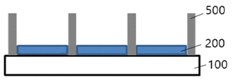
도 1 내지 4는 본 발명의 일 실시예에 따른 적층체를 설명하기 위한 단면도이다.
도 5는 본 발명의 다른 실시예에 따른 적층체를 설명하기 위한 단면도이다.
도 6은 본 발명의 실시예 20에 대한 잉크젯 공정특성을 평가한 사진이다.
도 7은 본 발명의 비교예 18에 대한 잉크젯 공정특성을 평가한 사진이다.
도 8은 본 발명의 비교예 16에 대한 화소 박리성을 평가한 사진이다.1 to 4 are cross-sectional views for explaining a laminate according to an embodiment of the present invention.
5 is a cross-sectional view for explaining a laminate according to another embodiment of the present invention.
6 is a photograph of evaluating inkjet process characteristics for Example 20 of the present invention.
7 is a photograph of evaluating inkjet process characteristics for Comparative Example 18 of the present invention.
8 is a photograph evaluating the pixel peelability of Comparative Example 16 of the present invention.
본 발명은 기재; 상기 기재상에 형성된 광원; 상기 광원상에 형성된 광굴절층; 및 상기 광굴절층 상에 형성된 색변환 잉크층을 포함하고, 상기 색변환 잉크층의 굴절률은 광굴절층의 굴절률보다 0.3 이상 작으며, 상기 광굴절층과 색변환 잉크층의 굴절률 차이(제1 굴절률 차이)가 광원의 최상부층과 광굴절층의 굴절률 차이(제2 굴절률 차이)보다 더 큰 적층체를 제공한다.The present invention is a substrate; a light source formed on the substrate; a light refractive layer formed on the light source; and a color conversion ink layer formed on the light refractive layer, wherein the refractive index of the color conversion ink layer is 0.3 or more smaller than the refractive index of the light refractive layer, and the refractive index difference between the light refractive layer and the color conversion ink layer (first and provide a laminate in which the refractive index difference) is greater than the refractive index difference (second refractive index difference) between the uppermost layer of the light source and the light refractive layer.
또한, 본 발명은 기재상에 광원을 형성하는 단계; 상기 광원 상에 광굴절층을 형성하는 단계; 및 상기 광굴절층 상에 색변환 잉크층을 형성하는 단계를 포함하고, 상기 상기 색변환 잉크층의 굴절률은 광굴절층의 굴절률보다 0.3 이상 작으며, 상기 광굴절층과 색변환 잉크층의 굴절률 차이(제1 굴절률 차이)가 광원의 최상부층과 광굴절층의 굴절률 차이(제2 굴절률 차이)보다 더 큰 적층체의 제조방법을 제공한다.In addition, the present invention comprises the steps of forming a light source on a substrate; forming a light refraction layer on the light source; and forming a color conversion ink layer on the light refractive layer, wherein the refractive index of the color conversion ink layer is 0.3 or more smaller than the refractive index of the light refractive layer, and the refractive index of the light refractive layer and the color conversion ink layer Provided is a method of manufacturing a laminate in which the difference (first refractive index difference) is greater than the refractive index difference (second refractive index difference) between the uppermost layer of the light source and the light refractive layer.
또한, 본 발명은 상기 적층체를 포함하는 화상표시장치를 제공한다.In addition, the present invention provides an image display device including the laminate.
본 발명의 적층체는 광원과 색변환 잉크층 사이에 색변환 잉크층과 일정한 굴절률 차이를 갖고, 상기 광굴절층과 색변환 잉크층의 굴절률 차이(제1 굴절률 차이)가 광원의 최상부층과 광굴절층의 굴절률 차이(제2 굴절률 차이)보다 더 크며, 특정 범위의 표면에너지를 갖는 광굴절층을 형성함으로써, 보다 적인 양의 잉크를 사용하여 색변환 잉크층을 형성할 수 있고, 상기 형성된 색변환 잉크층이 적층체로부터 박리되는 문제점을 방지할 수 있으며, 이를 포함하는 화상표시장치의 휘도를 향상시킬 수 있음을 실험적으로 확인하여 본 발명을 완성하였다.The laminate of the present invention has a certain refractive index difference with the color conversion ink layer between the light source and the color conversion ink layer, and the difference in refractive index between the light refractive layer and the color conversion ink layer (first refractive index difference) is the uppermost layer of the light source and the light The color conversion ink layer can be formed using a smaller amount of ink by forming the light refraction layer that is larger than the refractive index difference (second refractive index difference) of the refractive layer and has a surface energy in a specific range, and the formed color The present invention was completed by experimentally confirming that it is possible to prevent the conversion ink layer from being peeled off from the laminate and to improve the luminance of an image display device including the same.
본 발명의 장점 및 특징, 그리고 그것들을 달성하는 방법은 첨부한 도면과 함께 상세하게 후술되어 있는 실시예들을 참조하면 명확해질 것이다. 본 발명은 이하에서 개시되는 실시예들에 한정되는 것이 아니라 다양한 형태로 구현될 수 있다. 본 실시예들은 본 발명의 개시가 완전하도록 하며, 본 발명이 속하는 기술분야에서 통상의 지식을 가진 자에게 발명의 범주를 완전하게 알려주기 위해 제공한 것이다.Advantages and features of the present invention, and methods for achieving them, will become apparent with reference to the embodiments described below in detail in conjunction with the accompanying drawings. The present invention is not limited to the embodiments disclosed below, but may be implemented in various forms. The present embodiments are provided to complete the disclosure of the present invention, and to completely inform those of ordinary skill in the art to the scope of the present invention.
본 발명의 실시 예들을 설명하기 위한 도면에 개시된 형상, 크기, 비율, 각도, 개수 등은 예시적인 것이므로 본 발명이 도시된 사항에 한정되는 것은 아니다. 명세서 전체에 걸쳐 동일 참조 부호는 동일 구성 요소를 지칭한다.The shapes, sizes, proportions, angles, numbers, etc. disclosed in the drawings for explaining the embodiments of the present invention are exemplary, and thus the present invention is not limited to the illustrated matters. Like reference numerals refer to like elements throughout.
본 발명을 설명함에서, 관련된 공지 기능 혹은 구성에 대한 구체적인 설명이 본 발명의 요지를 불필요하게 흐릴 수 있다고 판단되는 경우, 그 상세한 설명을 생략한다. 본 명세서 상에서 언급된 '포함한다', '갖는다', '이루어진다' 등이 사용되는 경우 ' ~ 만'이 사용되지 않는 이상 다른 부분이 추가될 수 있다.In describing the present invention, if it is determined that a detailed description of a related known function or configuration may unnecessarily obscure the gist of the present invention, the detailed description thereof will be omitted. When 'including', 'having', 'consisting', etc. mentioned in this specification are used, other parts may be added unless 'only' is used.
구성 요소를 해석함에서, 위치 관계에 대한 설명일 경우, 예를 들어, ' ~ 상에', ' ~ 상부에', ' ~ 하부에', ' ~ 옆에' 등으로 두 부분의 위치 관계가 설명되는 경우, '바로' 또는 '직접'이 사용되지 않는 이상 두 부분 사이에 하나 이상의 다른 구성 요소가 위치할 수도 있다.In analyzing the components, in the case of a description of the positional relationship, for example, the positional relationship of the two parts is Where described, one or more other components may be positioned between two parts unless 'directly' or 'directly' is used.
본 발명의 여러 실시예들의 각각 특징들이 부분적으로 또는 전체적으로 서로 결합 또는 조합 가능하며, 기술적으로 다양한 연동 및 구동할 수 있다. 또한, 각 실시예들이 서로에 대하여 독립적으로 실시 가능할 수도 있고 연관 관계로 함께 실시 가능할 수도 있다.Each feature of the various embodiments of the present invention may be partially or wholly combined or combined with each other, and may be technically various interlocking and driving. In addition, each of the embodiments may be implemented independently of each other or may be implemented together in a related relationship.
이하, 도면을 참조하여 본 발명의 구체적인 실시형태를 설명하기로 한다. 다만, 본 명세서에 첨부되는 다음의 도면들은 본 발명의 바람직한 실시예를 예시하는 것이며, 전술한 발명의 내용과 함께 본 발명의 기술사상을 더욱 이해시키는 역할을 하는 것이므로, 본 발명은 그러한 도면에 기재된 사항에만 한정되어 해석되어서는 아니된다.Hereinafter, specific embodiments of the present invention will be described with reference to the drawings. However, the following drawings attached to the present specification illustrate preferred embodiments of the present invention, and serve to further understand the technical spirit of the present invention together with the above-described content of the present invention, so the present invention is described in such drawings It should not be construed as being limited only to the matters.
적층체laminate
본 발명의 적층체는 기재(100), 상기 기재상에 형성된 광원(200), 상기 광원상에 형성된 광굴절층(300) 및 상기 광굴절층 상에 형성된 색변환 잉크층(400)을 포함하며, 상기 기재상에 광원을 노출하는 개구부를 갖도록 형성된 격벽(500)을 포함할 수 있다. The laminate of the present invention includes a
상기 기재상에 형성된 광원(200)은, 광원이 기재의 상부 면에 형성된 구조와, 광원이 기재 내에 구비되어 기재의 상부면과 광원의 상부면이 일치하는 구조를 모두 포함하는 의미이다.The
도 4는 본 발명의 일 실시예에 따른 적층체를 설명하기 위한 단면도로, 기재(100), 상기 기재의 상부에 형성된 광원(200), 상기 광원상에 형성된 광굴절층(300) 및 상기 광굴절층 상에 형성된 색변환 잉크층(400)을 포함하고, 상기 기재상에 광원을 노출하는 개구부를 갖도록 형성된 격벽(500)을 포함한다.4 is a cross-sectional view for explaining a laminate according to an embodiment of the present invention, a
기재(100)는 화상표시장치 분야에서 사용되는 일반적인 기재가 사용될 수 있으며, 플렉서블한 소재가 바람직하게 사용될 수 있다. 예를 들면, 사이클로 올레핀 중합체(COP, cyclo olefine polymer), 폴리에틸렌테레프탈레이트(PET polyethyelene terepthalate), 폴리아크릴레이트(PAR, polyacrylate rubber), 폴리에테르이미드(PEI, polyether lmide), 폴리에틸렌나프탈레이트(PEN, poly(ethylene naphthalate)), 폴리페닐렌설파이드(PPS, polyphenylene sulfide), 폴리알릴레이트(polyallylate), 폴리이미드(PI, polyimide), 셀룰로오스 아세테이트 프로피오네이트(CAP, cellulose acetate propionate), 폴리에테르술폰(PES, polyethersulfone), 셀룰로오스 트리아세테이트(TAC, triacetate cellulose), 폴리카보네이트(PC, polycarbonate), 사이클로 올레핀 공중합체(COC, cyclo olefine copolymer), 폴리메틸메타크릴레이트(PMMA, polymethyl methacrylate) 등을 들 수 있으며, 바람직하게는 폴리에틸렌 테레프탈레이트(PET, polyethyelene terepthalate), 사이클로 올레핀 폴리머(COP, cyclo olefine polymer) 및 폴리이미드(PI, polyimide, 굴절율 1.72) 중 하나 이상으로 형성될 수 있다.As the
상기 기재의 두께는 10 내지 100㎛, 바람직하게는 20 내지 50㎛일 수 있다.The thickness of the substrate may be 10 to 100 μm, preferably 20 to 50 μm.
광원(200)은 상기 기재(100)상에 형성된다. 상기 광원(200)은 화상표시장치에 영상을 표시하는데 필요한 광을 발생시키는 것으로, 예를 들어, 냉음극 형광램프(cold cathode fluorescent lamp, CCFL), 외부전극 형광램프(external electrode fluorescent lamp, EEFL), 평판 형광램프(flat fluorescent lamp, FFL), 유기 발광 다이오드(organic light emitting diode, OLED), 발광 다이오드(light emitting diode, LED)일 수 있으나, 이에 한정되는 것은 아니다. 또한 광원은 광원의 상부에 다양한 층이 도입될 수 있으며, 일례로 유기 발광 다이오드의 경우, 음극과 양극 사이에 발광층이 위치하는 형태로 구성되나, 유기 발광 다이오드의 신뢰성을 확보하기 위하여 박막 봉지공정(Thin Film Encapsulation)을 진행한다. 박막 봉지공정은 외부환경(수분, 공기 등)으로부터 OLED 소자를 보호하기 위한 목적으로 적용하며, 이에 따른 대표적인 구조는 무기층과 유기층을 반복적으로 형성한 구조로, 최상부층에는 SiOx 무기층이 위치할 수 있다. The
광굴절층(300)은 상기 광원(200) 상에 형성된다. 상기 광굴절층(300)은 광원(200)과 후술할 색변환 잉크층(400) 사이에 형성되는 것을 특징으로 하며, 색변환 잉크층(400)을 형성함에 있어 잉크젯 공정특성을 향상시키고, 색변환 잉크층(400)에서 발생된 방출광 중 광원(200) 방향으로 향하는 광을 반사시켜 전체적인 휘도를 향상시키는 역할을 한다.The
상기 광굴절층(300)의 막두께는 1.0㎛ 이하인 것을 특징으로 할 수 있으며, 바람직하게는 0.05 내지 0.8㎛, 더욱 바람직하게는 0.1 내지 0.3㎛일 수 있다. 광굴절층(300)의 막두께가 상기 범위를 만족하는 경우, 색변환 잉크층(400)에서 발생된 방출광 중 광원(200) 방향으로 향하는 광을 효과적으로 반사시켜 전체적인 휘도를 더욱 향상시킬 수 있으므로 바람직하다.The
색변환 잉크층(400)은 상기 광굴절층(300)상에 형성된다. 상기 색변환 잉크층(400)은 광원(200)으로부터 입사된 빛의 파장을 다른 특정 파장의 빛으로 변환한다. 이와 같은 빛의 파장 변환을 위하여 색변환 잉크층(400)은 양자점을 포함하며, 상기 양자점은 광원으로부터의 빛을 녹색 또는 적색으로 변환하여 산란시킨다. The color
양자점을 포함하는 색변환 잉크층(400)은, 착색제를 포함하는 기존의 컬러필터와 달리, 색변환 효율을 고려하여 약 5㎛ 내지 15㎛의 두께로 형성될 필요가 있다. 이와 같이, 색변환 잉크층(400)의 두께가 두꺼워짐에 따라, 잉크젯 공정을 통해 색변환 잉크층(400)을 형성할 경우, 더 많은 양의 잉크를 젯팅해야하므로 공정특성이 저하되는 문제점이 있다. 또한, 색변환 잉크층(400)의 두께가 두꺼워질수록, 색변환 잉크층(400)이 하부층에 접촉하는 면적 대비 체적이 증가하게 되므로, 색변환 잉크층의 하부층에 대한 부착성이 저하되어 적층체로부터 색변환 잉크층(400)이 박리되는 문제점이 있다.Unlike a conventional color filter including a colorant, the color
본 발명의 적층체는 광굴절층(300)의 표면에너지가 24.9 내지 43.3 dyne/㎝인 것을 특징으로 할 수 있으며, 더욱 바람직하게는 28.8 내지 35.5 dyne/㎝일 수 있다. 광굴절층(300)의 표면에너지가 상기 범위를 갖도록 제어되는 경우, 잉크젯 공정을 통해 색변환 잉크층(400)을 형성함에 있어서, 보다 적은 양의 잉크를 사용하여 화소부를 모두 충진할 수 있어 공정속도를 향상시킬 수 있고, 젯팅 불량 등의 문제점을 방지할 수 있는 등 전반적으로 잉크젯 공정특성이 향상될 수 있으며, 형성된 색변환 잉크층(400)이 적층체로부터 박리되는 것을 방지할 수 있으므로 바람직하다.The laminate of the present invention may be characterized in that the surface energy of the
한편, 양자점으로부터 산란된 빛은 양자점이 가진 특성상 모든 방향을 향해 산란되며, 이들 중 기재(100) 방향으로 산란된 빛을 반사 내지 굴절시켜 화상표시장치의 영상 표시에 기여할 수 있도록 한다면 광 이용 효율을 향상시킬 수 있다.On the other hand, the light scattered from the quantum dots is scattered in all directions due to the characteristics of the quantum dots, and among them, the light use efficiency can be improved if the light scattered in the direction of the
본 발명의 적층체는 광굴절층(300)이 색변환 잉크층(400)보다 더 작은 굴절률을 가지는 것을 특징으로 할 수 있으며, 바람직하게는 광굴절층(300)이 색변환 잉크층(400)보다 0.3 이상 작은 굴절률을 가질 수 있다. 이와 같이 광굴절층(300)이 색변환 잉크층(400)보다 더 작은 굴절률을 가지는 경우, 색변환 잉크층의 양자점에 의해 산란된 빛 중 기재(100) 방향으로 산란된 빛을 반대 방향으로 반사 내지 굴절시킬 수 있으며, 이에 따라 화상표시장치의 휘도를 향상시킬 수 있으므로 바람직하다. The laminate of the present invention may be characterized in that the
상기 색변환 잉크층(400)은 굴절률이 1.8 내지 2.0일 수 있다. The color
또한, 상기 광굴절층(300)은 굴절률이 1.33 내지 1.5일 수 있으며, 바람직하게는 1.33 내지 1.4일 수 있다. 광굴절층(300)의 굴절률이 상기 범위를 만족하는 경우 색변환 잉크층(400)보다 더 작은 굴절률을 가지도록 조절할 수 있으며, 이에 따라 화상표시장치의 휘도를 향상시킬 수 있으므로 바람직하다.In addition, the refractive index of the light
또한, 본 발명의 적층체는 광굴절층(300)과 색변환 잉크층(400)의 굴절률 차이(이하, '제1 굴절률 차이'라고 한다)가 광원(200)의 최상부층과 광굴절층(300)의 굴절률 차이(이하, '제2 굴절률 차이'라고 한다)보다 더 큰 것을 특징으로 한다. 제1 굴절률 차이가 제2 굴절률 차이가 보다 더 큰 경우, 전반사 각도가 개선되어 제품의 휘도가 개선되는 효과를 극대화 할 수 있으므로 바람직하다.In addition, in the laminate of the present invention, the difference in refractive index between the light
상기 광원(200)의 최상부층은 굴절률이 1.45 내지 1.55일 수 있으며, 바람직하게는 1.48 내지 1.52일 수 있다. 광원(200)의 최상부층의 굴절률이 상기 범위를 만족하는 경우, 광원(200)의 최상부층이 광굴절층(300)보다 더 큰 굴절률을 가지도록 조절할 수 있으므로 바람직하다.The uppermost layer of the
격벽(500)은 색변환 잉크층을 채우기 위한 각 화소영역을 구획하는 둑과 같은 역할을 하며, 상기 기재(100)상에 광원(200)을 노출하는 개구부를 갖도록 형성된다. The
위에서 설명한 바와 같이, 색변환 잉크층(400)은 변환 효율로 인하여 약 5㎛ 내지 15㎛의 막 두께로 형성될 필요가 있으므로, 격벽(500) 역시 약 5㎛ 내지 15㎛의 막 두께로 형성될 필요가 있다.As described above, since the color
도 5는 본 발명의 다른 실시예에 따른 적층체를 설명하기 위한 단면도로, 광원(200)을 구비하는 기재(100), 상기 광원상에 형성된 광굴절층(300) 및 상기 광굴절층 상에 형성된 색변환 잉크층(400)을 포함하고, 상기 기재상에 광원을 노출하는 개구부를 갖도록 형성된 격벽(500)을 포함한다. 이 경우에도, 광굴절층(300)은 광원(200)의 최상부층과 맞닿는 구조를 갖는다. 따라서, 상기에서 설명된 제1 굴절률 차이 및 제2 굴절률 차이에 대한 설명은 해당 실시예의 구조에도 동일하게 적용될 수 있다.5 is a cross-sectional view for explaining a laminate according to another embodiment of the present invention. It includes the formed color
이와 같이, 본 발명의 적층체에 있어서, 광원(200)은 도 4에서와 같이 기재(100)의 상부 면에 형성되는 구조일 수 있고, 도 5에서와 같이 기재 내에 구비되어 기재의 상부면과 광원의 상부면이 일치하는 구조일 수 있으며, 이는 광원의 구체적인 종류 등에 따라 적절히 선택될 수 있다.As such, in the laminate of the present invention, the
광굴절층 형성용 조성물Composition for forming a light refractive layer
상기 광굴절층(300)은 광굴절층 형성용 조성물로부터 형성되며, 상기 광굴절층 형성용 조성물은 산란 입자를 포함할 수 있다. The
상기 산란 입자는 이 분야에 공지된 산란 입자를 특별한 제한 없이 선택하여 사용할 수 있으나, 예를 들어 Al2O3, SiO2, ZnO, ZrO2, BaTiO3, TiO2, Ta2O5, Ti3O5, ITO, IZO, ATO, ZnO-Al, Nb2O3, SnO 및 MgO로 이루어진 군에서 선택되는 1종 이상을 포함할 수 있으며, 필요에 따라 아크릴레이트와 같은 불포화 결합을 갖는 화합물로 표면 처리된 재질도 사용 가능하며, 바람직하게는 저굴절 실리콘 입자 및 내부가 비어있는 중공 입자 중 하나 이상을 사용할 수 있다. 상기 중공 입자는 중공실리카 중공 이산화티탄, 금-알루미늄-이산화티타늄-폴리메타아크릴레이트 중공 입자 등을 사용할 수 있다.As the scattering particles, scattering particles known in the art may be selected and used without particular limitation, for example, Al 2 O 3 , SiO 2 , ZnO, ZrO 2 , BaTiO 3 , TiO 2 , Ta 2 O 5 , Ti 3 O 5 , ITO, IZO, ATO, ZnO-Al, Nb 2 O 3 , may include at least one selected from the group consisting of SnO and MgO, and if necessary, a compound having an unsaturated bond such as acrylate. A treated material may also be used, and preferably, one or more of low-refractive silicon particles and hollow particles with an empty interior may be used. The hollow particles may include hollow silica hollow titanium dioxide, gold-aluminum-titanium dioxide-polymethacrylate hollow particles, and the like.
상기 산란 입자의 함량은, 특별히 한정되는 것은 아니나, 상기 광굴절층 형성용 조성물 중 고형분 총 중량에 대하여 0.1 내지 50 중량%, 바람직하게는 0.5 내지 20 중량%로 포함될 수 있다. 상기 산란 입자가 상기 범위 내로 포함될 경우 광굴절층(300)의 굴절률을 목적하는 범위 내로 조절하는데 유리할 수 있다. The content of the scattering particles is not particularly limited, but may be included in an amount of 0.1 to 50% by weight, preferably 0.5 to 20% by weight, based on the total weight of the solid content in the composition for forming the light refraction layer. When the scattering particles are included within the above range, it may be advantageous to adjust the refractive index of the
또한, 상기 광굴절층 형성용 조성물은 바인더 수지, 광중합성 화합물, 광중합 개시제 및 용제를 더 포함할 수 있다.In addition, the composition for forming the photorefractive layer may further include a binder resin, a photopolymerizable compound, a photopolymerization initiator, and a solvent.
상기 바인더 수지는 아크릴계 수지, 실록산계 수지, 폴리이소프렌, 비닐계 수지, 에폭시계 수지, 우레탄계 수지, 셀룰로오스계 수지 및 페릴렌계 수지 등으로 이루어질 수 있으며, 바람직하게는 아크릴계 수지 및 실록산계 수지를 함께 포함하는 것일 수 있다.The binder resin may be made of an acrylic resin, a siloxane-based resin, polyisoprene, a vinyl-based resin, an epoxy-based resin, a urethane-based resin, a cellulose-based resin, and a perylene-based resin, preferably including an acrylic resin and a siloxane-based resin. may be doing
상기 바인더 수지의 함량은, 특별히 한정되는 것은 아니나, 상기 광굴절층 형성용 조성물 중 고형분 총 중량에 대하여, 20 내지 70 중량%, 바람직하게는 30 내지 60 중량%로 포함될 수 있다. 상기 바인더 수지가 상기 범위 내로 포함될 경우 현상액에 대한 용해성이 충분하여 경화막 형성이 용이하며, 현상시에 노광부의 화소 부분의 막 감소가 방지되어 비노광부의 누락성이 양호해지므로 바람직하다. The content of the binder resin is not particularly limited, but may be included in an amount of 20 to 70% by weight, preferably 30 to 60% by weight, based on the total weight of the solid content in the composition for forming the light refraction layer. When the binder resin is contained within the above range, the solubility in the developer is sufficient to facilitate the formation of a cured film, and the film reduction of the pixel portion of the exposed portion is prevented during development, so that the omission property of the unexposed portion is improved.
상기 광중합성 화합물은, 광 및 후술할 광중합 개시제의 작용으로 중합할 수 있는 화합물로서, 당 업계에서 사용되는 것을 특별한 제한 없이 사용할 수 있으며, 예를 들면, 단관능 단량체, 2관능 단량체, 그 밖의 다관능 단량체 등을 들 수 있다. The photopolymerizable compound is a compound that can be polymerized by the action of light and a photopolymerization initiator to be described later, and those used in the art may be used without particular limitation, for example, monofunctional monomers, difunctional monomers, and other polyfunctional monomers. A functional monomer etc. are mentioned.
상기 단관능 단량체의 종류는 특별히 한정되지 않으며, 예를 들면 노닐페닐카르비톨아크릴레이트, 2-히드록시-3-페녹시프로필아크릴레이트, 2-에틸헥실카르비톨아크릴레이트, 2-히드록시에틸아크릴레이트, N-비닐피롤리돈 등을 들 수 있다.The type of the monofunctional monomer is not particularly limited, for example, nonylphenyl carbitol acrylate, 2-hydroxy-3-phenoxypropyl acrylate, 2-ethylhexyl carbitol acrylate, 2-hydroxyethyl acryl Late, N-vinylpyrrolidone, etc. are mentioned.
상기 2관능 단량체의 종류는 특별히 한정되지 않으며, 예를 들면, 1,6-헥산디올디(메타)아크릴레이트, 에틸렌글리콜디(메타)아크릴레이트, 네오펜틸글리콜디(메타)아크릴레이트, 트리에틸렌글리콜디(메타)아크릴레이트, 비스페놀 A의 비스(아크릴로일옥시에틸)에테르, 3-메틸펜탄디올디(메타)아크릴레이트, 비스페녹시에탄올 플루오렌계 화합물 등을 들 수 있다.The type of the bifunctional monomer is not particularly limited, and for example, 1,6-hexanediol di (meth) acrylate, ethylene glycol di (meth) acrylate, neopentyl glycol di (meth) acrylate, triethylene Glycol di(meth)acrylate, bis(acryloyloxyethyl)ether of bisphenol A, 3-methylpentanediol di(meth)acrylate, bisphenoxyethanol fluorene type compound, etc. are mentioned.
상기 다관능 단량체의 종류는 특별히 한정되지 않으며, 예를 들면, 트리메틸올프로판트리(메타)아크릴레이트, 에톡실레이티드트리메틸올프로판트리(메타)아크릴레이트, 프로폭실레이티드트리메틸올프로판트리(메타)아크릴레이트, 펜타에리스리톨트리(메타)아크릴레이트, 펜타에리스리톨테트라(메타)아크릴레이트, 디펜타에리스리톨트리(메타)아크릴레이트, 디펜타에리스리톨펜타(메타)아크릴레이트, 에톡실레이티드디펜타에리스리톨헥사(메타)아크릴레이트, 프로폭실레이티드디펜타에리스리톨헥사(메타)아크릴레이트, 디펜타에리스리톨헥사(메타)아크릴레이트 등을 들 수 있다. 이들 중에서 2관능 이상의 다관능 단량체가 바람직하게 사용될 수 있다.The type of the polyfunctional monomer is not particularly limited, and for example, trimethylolpropane tri(meth)acrylate, ethoxylated trimethylolpropane tri(meth)acrylate, propoxylated trimethylolpropane tri(meth) ) acrylate, pentaerythritol tri (meth) acrylate, pentaerythritol tetra (meth) acrylate, dipentaerythritol tri (meth) acrylate, dipentaerythritol penta (meth) acrylate, ethoxylated dipentaerythritol hexa (meth)acrylate, propoxylated dipentaerythritol hexa(meth)acrylate, dipentaerythritol hexa(meth)acrylate, etc. are mentioned. Among them, a polyfunctional monomer having a bifunctional or higher function may be preferably used.
상기 광중합성 화합물의 시판되는 예로는 신나카무라사의 A9550, 일본화학㈜사의 KAYARAD DPHA, 켐톤사의 CHTH-2553 등이 있으나, 이에 한정되지는 않는다.Commercially available examples of the photopolymerizable compound include A9550 from Shin-Nakamura, KAYARAD DPHA from Nippon Chemical Co., Ltd., CHTH-2553 from Kempton, and the like, but are not limited thereto.
상기 광중합성 화합물의 함량은, 특별히 한정되는 것은 아니나, 상기 광굴절층 형성용 조성물 중 고형분 총 중량에 대하여 20 내지 70 중량%, 바람직하게는 30 내지 60 중량%로 포함될 수 있다. 광중합성 화합물이 상기 범위 내로 포함될 경우 광굴절층의 강도나 평활성 측면에서 바람직하다.The content of the photopolymerizable compound is not particularly limited, but may be included in an amount of 20 to 70% by weight, preferably 30 to 60% by weight, based on the total weight of the solid content in the composition for forming a photorefractive layer. When the photopolymerizable compound is included within the above range, it is preferable in terms of strength or smoothness of the light-refractive layer.
상기 광중합 개시제는 이 분야에 공지된 광중합 개시제를 특별한 제한 없이 선택하여 사용할 수 있다. 예컨대 아세토페논계, 벤조페논계, 트리아진계, 티오크산톤계, 옥심계, 벤조인계, 비이미다졸계 화합물 등을 사용할 수 있다.As the photopolymerization initiator, a photopolymerization initiator known in the art may be selected and used without particular limitation. For example, acetophenone-based, benzophenone-based, triazine-based, thioxanthone-based, oxime-based, benzoin-based, biimidazole-based compounds and the like may be used.
예를 들면, 상기 옥심계 화합물로는 o-에톡시카르보닐-α-옥시이미노-1-페닐프로판-1-온 등을 사용할 수 있으며, 시판품으로 Basf사의 OXE-01, OXE-02, OXE-03 등이 있으나, 이에 한정되지는 않는다. 상기 광중합 개시제는 단독 또는 2종 이상을 혼합하여 사용할 수 있다.For example, as the oxime-based compound, o-ethoxycarbonyl-α-oxyimino-1-phenylpropan-1-one and the like may be used, and Basf's OXE-01, OXE-02, and OXE- are commercially available products. 03, but is not limited thereto. The photopolymerization initiator may be used alone or in combination of two or more.
상기 광중합 개시제의 함량은 감광성 수지 조성물 중 고형분 총 중량에 대하여 0.01 내지 10 중량%, 바람직하게는 0.01 내지 5 중량%로 포함될 수 있다. 광중합 개시제가 상기 범위 내로 포함되는 경우, 광중합 반응 속도가 적정하여 전체 공정 시간의 증가가 방지되고, 과반응에 의한 최종 경화막의 물성 저하를 방지할 수 있으므로 바람직하다.The content of the photopolymerization initiator may be 0.01 to 10 wt%, preferably 0.01 to 5 wt%, based on the total weight of the solid content in the photosensitive resin composition. When the photopolymerization initiator is included within the above range, it is preferable because the photopolymerization reaction rate is appropriate to prevent an increase in the overall process time and to prevent deterioration of physical properties of the final cured film due to overreaction.
상기 용제는 당 업계에서 사용되는 것을 특별한 제한 없이 사용할 수 있으며, 구체적으로 에틸렌글리콜 모노메틸에테르, 에틸렌글리콜 모노에틸 에테르, 에틸렌글리콜 모노프로필에테르, 에틸렌글리콜 모노부틸에테르 등의 에틸렌글리콜 모노알킬에테르류, 디에틸렌글리콜 디메틸에테르, 디에틸렌글리콜 디에틸에테르, 디에틸렌글리콜 디프로필에테르, 디에틸렌글리콜 디부틸에테르 등의 디에틸렌글리콜 디알킬에테르류; 메틸셀로솔브아세테이트, 에틸셀로솔브아세테이트 등의 에틸렌글리콜 알킬에테르아세테이트류; 프로필렌글리콜 모노메틸에테르아세테이트, 프로필렌글리콜 모노에틸에테르아세테이트, 프로필렌글리콜모노프로필에테르아세테이트, 등의 알킬렌글리콜 알킬에테르아세테이트류; 메톡시부틸아세테이트, 메톡시펜틸아세테이트 등의 알콕시알킬아세테이트류; 벤젠, 톨루엔, 크실렌, 메시틸렌 등의 방향족 탄화수소류; 메틸에틸케톤, 아세톤, 메틸아밀케톤, 메틸이소부틸케톤, 시클로헥사논 등의 케톤류, 에탄올, 프로판올, 부탄올, 헥산올, 시클로헥산올, 에틸렌글리콜, 글리세린 등의 알코올류; 3-에톡시프로피온산에틸, 3-메톡시프로피온산메틸 등의에스테르류; γ-부티롤락톤 등의 환상 에스테르류 등을 들 수 있다.The solvent can be used without any particular limitation to those used in the art, specifically ethylene glycol monoalkyl ethers such as ethylene glycol monomethyl ether, ethylene glycol monoethyl ether, ethylene glycol monopropyl ether, ethylene glycol monobutyl ether, diethylene glycol dialkyl ethers such as diethylene glycol dimethyl ether, diethylene glycol diethyl ether, diethylene glycol dipropyl ether, and diethylene glycol dibutyl ether; ethylene glycol alkyl ether acetates such as methyl cellosolve acetate and ethyl cellosolve acetate; alkylene glycol alkyl ether acetates such as propylene glycol monomethyl ether acetate, propylene glycol monoethyl ether acetate, and propylene glycol monopropyl ether acetate; alkoxyalkyl acetates such as methoxybutyl acetate and methoxypentyl acetate; aromatic hydrocarbons such as benzene, toluene, xylene, and mesitylene; ketones such as methyl ethyl ketone, acetone, methyl amyl ketone, methyl isobutyl ketone and cyclohexanone; alcohols such as ethanol, propanol, butanol, hexanol, cyclohexanol, ethylene glycol and glycerin; esters such as ethyl 3-ethoxypropionate and methyl 3-methoxypropionate; Cyclic esters, such as (gamma)-butyrolactone, etc. are mentioned.
상기 용제는 도포성 및 건조성면에서 바람직하게는 상기 용제 중에서 비점이 100℃ 내지 200℃인 유기 용제를 사용할 수 있고, 바람직하게는 프로필렌글리콜모노메틸에테르아세테이트를 사용할 수 있다. The solvent may be an organic solvent having a boiling point of 100°C to 200°C among the solvents, preferably propylene glycol monomethyl ether acetate, in terms of coatability and drying properties.
상기 용제의 함량은, 특별히 한정되는 것은 아니나, 광굴절층 형성용 조성물 총 중량에 대하여 60 내지 90 중량%, 바람직하게는 70 내지 85 중량%로 포함될 수 있다. 상기 용제가 상기 함량 범위 내로 포함되는 경우, 롤 코터, 스핀 코터, 슬릿 앤드 스핀 코터, 슬릿 코터(다이 코터라고도 하는 경우가 있음), 잉크젯 등의 도포 장치로 도포했을 때 도포성이 양호해지는 효과를 제공하므로 바람직하다.The content of the solvent is not particularly limited, but may be included in an amount of 60 to 90% by weight, preferably 70 to 85% by weight, based on the total weight of the composition for forming a photorefractive layer. When the solvent is contained within the above content range, the effect of improving the applicability when applied with an application device such as a roll coater, a spin coater, a slit and spin coater, a slit coater (sometimes referred to as a die coater), an inkjet, etc. It is preferable to provide
상기 광굴절층 형성용 조성물은 그 목적을 저해하지 않는 범위 내에서 첨가제를 더 포함할 수도 있다. 상기 첨가제는 사용자의 필요에 따라 더 포함될 수 있는 구성으로 그 종류를 본 발명에서 특별히 한정하는 것은 아니나, 예를 들면 광굴절층 형성용 조성물의 코팅성 또는 밀착성을 증진시키기 위한 밀착촉진제 또는 계면활성제 등을 들 수 있다.The composition for forming the light refraction layer may further include an additive within a range that does not impair its purpose. The additive is a configuration that can be further included according to the needs of the user, and the type is not particularly limited in the present invention, but for example, an adhesion promoter or surfactant for enhancing the coatability or adhesion of the composition for forming a light refraction layer, etc. can be heard
상기 밀착촉진제는 기판과의 밀착성을 높이기 위하여 첨가될 수 있는 것으로서 카르복실기, 메타크릴로일기, 이소시아네이트기, 에폭시기 및 이들의 조합으로 이루어진 군에서 선택되는 반응성 치환기를 갖는 실란 커플링제를 포함할 수 있으나 이에 한정되는 것은 아니다. 예컨대, 상기 실란 커플링제는 트리메톡시실릴 벤조산, γ-메타크릴 옥시프로필 트리메톡시 실란, 비닐트리아세톡시실란, 비닐 트리메톡시실란, γ-이소시아네이트 프로필트리에톡시실란, γ-글리시독시 프로필 트리메톡시실란, β-(3,4-에폭시시클로헥실)에틸트리메톡시실란 등을 들 수 있으며, 이것들은 단독 및 2종 이상 조합하여 사용할 수 있다.The adhesion promoter may include a silane coupling agent having a reactive substituent selected from the group consisting of a carboxyl group, a methacryloyl group, an isocyanate group, an epoxy group, and combinations thereof, which may be added to increase adhesion to the substrate. It is not limited. For example, the silane coupling agent is trimethoxysilyl benzoic acid, γ-methacryl oxypropyl trimethoxy silane, vinyltriacetoxysilane, vinyl trimethoxysilane, γ-isocyanate propyltriethoxysilane, γ-glycidoxy and propyl trimethoxysilane and β-(3,4-epoxycyclohexyl)ethyltrimethoxysilane, and these can be used alone or in combination of two or more.
상기 광굴절층 형성용 조성물이 상기 계면활성제를 포함하는 경우 코팅성이 보다 향상될 수 있는 이점이 있다. 예컨대 상기 계면활성제는 BM-1000, BM-1100(BM Chemie사 제), 프로라이드 FC-135/FC-170C/FC-430(스미토모 쓰리엠㈜ 제), SH-28PA/-190/SZ-6032(도레 시리콘㈜ 제), R-40, R-41, R-43, R-94, F-447, F-554, F-556(DIC사 제) 등의 불소계 계면활성제를 사용할 수 있으나, 이에 한정되지는 않는다.When the composition for forming the light refraction layer includes the surfactant, there is an advantage that coatability can be further improved. For example, the surfactant is BM-1000, BM-1100 (manufactured by BM Chemie), Proride FC-135/FC-170C/FC-430 (manufactured by Sumitomo 3M), SH-28PA/-190/SZ-6032 (manufactured by Sumitomo 3M) Toray Silicone Co., Ltd.), R-40, R-41, R-43, R-94, F-447, F-554, F-556 (manufactured by DIC), etc. not limited
색변환 잉크층 형성용 조성물Composition for forming a color conversion ink layer
상기 색변환 잉크층(400)은 색변환 잉크층 형성용 조성물로부터 형성되며, 상기 색변환 잉크층 형성용 조성물은 양자점을 포함할 수 있다.The color
상기 양자점은 전자가 전도대에서 가전자대로 전이하면서 특정한 색을 방출하는 입자상 물질일 수 있으며, 광 또는 전기에 의한 자극으로 발광할 수 있는 입자라면 특별히 한정되지 않으나, 예를 들어, II-VI족 반도체 화합물; III-V족 반도체 화합물; IV-VI족 반도체 화합물; IV족 원소 또는 이를 포함하는 화합물; 및 이들의 조합으로 이루어진 군에서 선택될 수 있으며, 이들은 단독 또는 2종 이상 혼합하여 사용할 수 있다. 본 발명의 일 실시예에서는 인듐포스파이드(InP)을 사용하였다. The quantum dot may be a particulate material that emits a specific color while electrons transition from the conduction band to the valence band, and is not particularly limited as long as it is a particle capable of emitting light when stimulated by light or electricity, for example, a group II-VI semiconductor compound; III-V semiconductor compounds; group IV-VI semiconductor compounds; Group IV element or a compound containing the same; And may be selected from the group consisting of combinations thereof, and these may be used alone or in mixture of two or more. In an embodiment of the present invention, indium phosphide (InP) was used.
상기 색변환 잉크층 형성용 조성물은 바인더 수지, 광중합성 화합물, 광중합 개시제 및 용제를 더 포함할 수 있으며, 상기 바인더 수지, 광중합성 화합물, 광중합 개시제 및 용제에 관한 설명은 상술한 광굴절층 형성용 조성물에서의 설명과 같다. The composition for forming the color conversion ink layer may further include a binder resin, a photopolymerizable compound, a photoinitiator and a solvent, and the description of the binder resin, the photopolymerizable compound, the photoinitiator and the solvent is for forming the photorefractive layer described above. As described in the composition.
또한, 상기 색변환 잉크층 형성용 조성물은 그 목적을 저해하지 않는 범위 내에서 첨가제를 더 포함할 수도 있다. 예를 들면 색변환 잉크층 형성용 조성물의 코팅성 또는 밀착성을 증진시키기 위한 밀착촉진제 또는 계면활성제 등을 들 수 있으며, 상기 밀착촉진제 및 계면활성제에 관한 설명은 상술한 광굴절층 형성용 조성물에서의 설명과 같다.In addition, the composition for forming the color conversion ink layer may further include an additive within a range that does not impair its purpose. For example, there may be mentioned an adhesion promoter or surfactant for enhancing the coatability or adhesion of the composition for forming a color conversion ink layer, and the description of the adhesion promoter and surfactant is described above in the composition for forming a light refraction layer. Same as description.
격벽 형성용 조성물Composition for forming barrier ribs
상기 격벽(500)은 격벽 형성용 조성물로부터 형성되며, 상기 격벽 형성용 조성물은 착색제를 포함할 수 있다.The
상기 착색제는 그 종류를 특별히 한정하는 것은 아니나, 백색 안료 및/또는 흑색 안료를 포함할 수 있다. 이와 같이, 백색 안료 및/또는 흑색 안료를 포함하는 격벽 형성용 조성물을 이용하여 격벽을 형성하는 경우, 흡광도는 낮추면서 투과율 및 반사율을 보다 향상시킬 수 있어 광효율이 우수한 이점이 있으므로 바람직하다.The type of the colorant is not particularly limited, but may include a white pigment and/or a black pigment. As described above, when the barrier rib is formed using the composition for forming barrier ribs including a white pigment and/or a black pigment, transmittance and reflectance can be further improved while reducing absorbance, and thus, it is preferable because the light efficiency is excellent.
상기 백색 안료는 그 종류를 특별히 한정하는 것은 아니나, C.I. 피그먼트 화이트 4, 5, 6, 6:1, 7, 18, 18:1, 19, 20, 22, 25, 26, 27 및 28으로 이루어진 군으로부터 선택되는 1종 이상을 포함할 수 있으며, 바람직하게는 C.I. 피그먼트 화이트 6을 포함할 수 있다.The type of the white pigment is not particularly limited, but C.I. Pigment White 4, 5, 6, 6:1, 7, 18, 18:1, 19, 20, 22, 25, 26, 27 and 28 may include at least one selected from the group consisting of, preferably Hage CI Pigment White 6 may be included.
상기 흑색 안료는 그 종류를 특별히 한정하는 것은 아니나, C.I. 피그먼트 블랙 1 및 7로부터 선택되는 1종 이상을 포함할 수 있고, 바람직하게는 C.I. 피그먼트 블랙 7을 포함할 수 있다.The type of the black pigment is not particularly limited, but C.I. It may include one or more selected from Pigment Black 1 and 7, preferably C.I. Pigment Black 7 may be included.
상기 착색제는, 필요에 따라 상기 백색 안료 또는 흑색 안료 외의 다른 안료 또는 염료를 포함할 수 있다. 상기 안료는 당해 분야에서 일반적으로 사용되는 유기 안료 또는 무기 안료를 사용할 수 있으며, 상기 염료는 유기용제에 대한 용해성을 가지는 것이라면 제한 없이 사용할 수 있다.The colorant may include other pigments or dyes other than the white pigment or the black pigment, if necessary. As the pigment, organic or inorganic pigments generally used in the art may be used, and the dye may be used without limitation as long as it has solubility in organic solvents.
본 발명에 따른 격벽 형성용 조성물은 바인더 수지, 광중합성 화합물, 광중합 개시제 및 용제를 더 포함할 수 있으며, 상기 바인더 수지, 광중합성 화합물, 광중합 개시제 및 용제에 관한 설명은 상술한 광굴절층 형성용 조성물에서의 설명과 같다. The composition for forming a barrier rib according to the present invention may further include a binder resin, a photopolymerizable compound, a photopolymerization initiator, and a solvent. As described in the composition.
또한, 상기 격벽 형성용 조성물은 그 목적을 저해하지 않는 범위 내에서 첨가제를 더 포함할 수도 있다. 예를 들면 격벽 형성용 조성물의 코팅성 또는 밀착성을 증진시키기 위한 밀착촉진제, 계면활성제 또는 발액제 등을 들 수 있으며, 상기 밀착촉진제 및 계면활성제에 관한 설명은 상술한 광굴절층 형성용 조성물에서의 설명과 같다.In addition, the composition for forming a barrier rib may further include an additive within a range that does not impair its purpose. For example, an adhesion promoter, a surfactant, or a liquid repellent agent for enhancing the coating property or adhesion of the composition for forming a barrier rib, etc. Same as description.
상기 발액제는 격벽의 표면에너지를 조절하기 위하여 첨가될 수 있는 것으로서, 불소계 내지 실리콘계 첨가제 등을 사용할 수 있으나 이에 한정되지 않는다.The liquid repellent may be added to control the surface energy of the barrier rib, and a fluorine-based or silicone-based additive may be used, but is not limited thereto.
적층체의 제조방법Method for manufacturing a laminate
본 발명은 기재상에 광원을 형성하는 단계; 상기 광원 상에 광굴절층을 형성하는 단계; 및 상기 광굴절층 상에 색변환 잉크층을 형성하는 단계를 포함하는 적층체의 제조방법을 제공한다. The present invention comprises the steps of forming a light source on a substrate; forming a light refraction layer on the light source; and forming a color conversion ink layer on the light refraction layer.
또한, 본 발명에 따른 적층체의 제조방법은, 상기 기재상에 광원을 형성하는 단계 이후, 상기 기재상에 광원을 노출하는 개구부를 갖는 격벽을 형성하는 단계를 더 포함하는 것을 특징으로 할 수 있다. In addition, the method for manufacturing a laminate according to the present invention may further include, after forming the light source on the substrate, forming a barrier rib having an opening for exposing the light source on the substrate. .
본 발명에 따른 적층체의 제조방법은, 광굴절층의 표면에너지가 24.9 내지 43.3 dyne/㎝인 것을 특징으로 할 수 있으며, 더욱 바람직하게는 28.8 내지 35.5 dyne/㎝일 수 있다. 광굴절층(300)의 표면에너지가 상기 범위를 갖도록 제어되는 경우, 잉크젯 공정을 통해 색변환 잉크층(400)을 형성함에 있어서, 보다 적은 양의 잉크를 사용하여 화소부를 모두 충진할 수 있어 공정속도를 향상시킬 수 있고, 젯팅 불량 등의 문제점을 방지할 수 있는 등 전반적으로 잉크젯 공정특성이 향상될 수 있으며, 형성된 색변환 잉크층(400)이 적층체로부터 박리되는 것을 방지할 수 있으므로 바람직하다.The method of manufacturing a laminate according to the present invention may be characterized in that the surface energy of the light refraction layer is 24.9 to 43.3 dyne/cm, and more preferably 28.8 to 35.5 dyne/cm. When the surface energy of the
또한, 본 발명에 따른 적층체의 제조방법은, 상기 광굴절층(300)의 굴절률이 색변환 잉크층(400)의 굴절률보다 작은 것을 특징으로 할 수 있으며, 바람직하게는 0.3 이상 작은 굴절률을 가질 수 있다. 이와 같이 광굴절층(300)이 색변환 잉크층(400)보다 더 작은 굴절률을 가지는 경우, 색변환 잉크층의 양자점에 의해 산란된 빛 중 기재(100) 방향으로 산란된 빛을 반대 방향으로 반사 내지 굴절시킬 수 있으며, 이에 따라 화상표시장치의 휘도를 향상시킬 수 있으므로 바람직하다.In addition, the method for manufacturing a laminate according to the present invention may be characterized in that the refractive index of the light
또한, 본 발명에 따른 적층체의 제조방법은, 광굴절층(300)과 색변환 잉크층(400)의 굴절률 차이(제1 굴절률 차이)가 광원(200)의 최상부층과 광굴절층(300)의 굴절률 차이(제2 굴절률 차이)보다 더 큰 것이 더욱 바람직하다. 제1 굴절률 차이가 제2 굴절률 차이가 보다 더 큰 경우, 전반사 각도가 개선되어 제품의 휘도가 개선되는 효과를 극대화 할 수 있으므로 바람직하다.In addition, in the manufacturing method of the laminate according to the present invention, the difference in refractive index (first refractive index difference) between the
화상표시장치image display device
본 발명의 다른 양태에 따른 화상표시장치는 전술한 적층체를 포함함으로써, 우수한 휘도를 가지고, 색변환 잉크층의 박리에 따른 불량이 없는 고품질의 화상표시장치를 제공할 수 있는 이점이 있다.The image display apparatus according to another aspect of the present invention has the advantage of providing a high-quality image display apparatus having excellent luminance and having no defects due to peeling of the color conversion ink layer by including the above-described laminate.
구체적으로, 상기 화상표시장치는 본 발명의 적층체 이외에도 광학 필름 등과 같이 통상적으로 화상표시장치에 포함될 수 있는 그 밖의 구성들을 포함할 수 있으며, 본 발명에서 이를 한정하지는 않는다. Specifically, the image display apparatus may include other components that may be included in an image display apparatus in general, such as an optical film, in addition to the laminate of the present invention, but the present invention is not limited thereto.
상기 화상표시장치는 구체적으로, 액정 디스플레이(액정표시장치; LCD), 유기 EL 디스플레이(유기 EL 표시장치, OLED 및 QLED 포함), 무기 발광다이오드 (LED) 디스플레이, 액정 프로젝터, 게임용 표시장치, 휴대전화 등의 휴대단말용 표시장치, 디지털 카메라용 표시장치, 카 네비게이션용 표시장치 등의 표시장치 등을 들 수 있으나, 이에 한정되는 것은 아니다.The image display device is specifically, a liquid crystal display (liquid crystal display device; LCD), an organic EL display (including an organic EL display device, OLED and QLED), an inorganic light emitting diode (LED) display, a liquid crystal projector, a game display device, a mobile phone display devices such as a display device for a portable terminal, such as a display device for a digital camera, a display device for a car navigation device, and the like, but are not limited thereto.
이하, 본 발명을 실시예에 기초하여 더욱 상세하게 설명하지만, 하기에 개시되는 본 발명의 실시 형태는 어디까지 예시로써, 본 발명의 범위는 이들의 실시 형태에 한정되지 않는다. 본 발명의 범위는 특허청구범위에 표시되었고, 더욱이 특허 청구범위 기록과 균등한 의미 및 범위 내에서의 모든 변경을 함유하고 있다. 또한, 이하의 실시예, 비교예에서 함유량을 나타내는 "%" 및 "부"는 특별히 언급하지 않는 한 질량 기준이다.Hereinafter, although this invention is demonstrated in more detail based on an Example, embodiment of this invention disclosed below is only an illustration to the last, and the scope of the present invention is not limited to these embodiments. The scope of the present invention is indicated in the claims, and moreover, it embraces all modifications within the meaning and scope equivalent to those recorded in the claims. In addition, in the following examples and comparative examples, "%" and "part" indicating the content are based on mass unless otherwise specified.
<실시예><Example>
합성예 1: 바인더 수지(B1)의 합성Synthesis Example 1: Synthesis of binder resin (B1)
교반기, 온도계 환류 냉각관, 적하 로트 및 질소 도입관을 구비한 플라스크를 준비하고, 한편, N-벤질말레이미드 15 중량부, 아크릴산 30 중량부, 사이클로헥실 메타크릴레이트 50 중량부, 메틸 메타크릴레이트 5 중량부, t-부틸퍼옥시-2-에틸헥사노에이트 4 중량부, 프로필렌글리콜모노메틸에테르아세테이트(이하, PGMEA라고도 함) 40 중량부를 투입 후 교반 혼합하여 모노머 적하 로트를 준비하고, n-도데칸디올 6 중량부, PGMEA 24 중량부를 넣고 교반 혼합하여 연쇄이동제 적하 로트를 준비했다.A flask equipped with a stirrer, a thermometer reflux cooling tube, a dropping funnel and a nitrogen introduction tube was prepared, while 15 parts by weight of N-benzylmaleimide, 30 parts by weight of acrylic acid, 50 parts by weight of cyclohexyl methacrylate, and methyl methacrylate 5 parts by weight, 4 parts by weight of t-butylperoxy-2-ethylhexanoate, and 40 parts by weight of propylene glycol monomethyl ether acetate (hereinafter also referred to as PGMEA) were added, stirred and mixed to prepare a monomer dropping lot, and n- 6 parts by weight of dodecanediol and 24 parts by weight of PGMEA were added and mixed with stirring to prepare a chain transfer agent dropping lot.
이후 플라스크에 PGMEA 395 중량부를 도입하고 플라스크내 분위기를 공기에서 질소로 치환한 후 교반하면서 플라스크의 온도를 90℃까지 승온하였다. 이어서 모노머 및 연쇄 이동제를 적하 로트로부터 적하를 개시했다. 적하는 90℃를 유지하면서 각각 2 시간 동안 진행하였고, 1 시간 후에 110℃로 승온하여 3 시간 유지한 뒤, 가스 도입관을 도입시켜, 산소/질소=5/95(v/v) 혼합 가스의 버블링을 개시하였다.Thereafter, 395 parts by weight of PGMEA was introduced into the flask, the atmosphere in the flask was substituted from air to nitrogen, and the temperature of the flask was raised to 90° C. while stirring. Then, the monomer and the chain transfer agent were started dripping from the dropping lot. The dripping was carried out for 2 hours while maintaining 90°C, and after 1 hour, the temperature was raised to 110°C and maintained for 3 hours, and then a gas introduction tube was introduced, and oxygen/nitrogen = 5/95 (v/v) mixed gas was produced. Bubbling was initiated.
이어서, 글리시딜메타크릴레이트 20 중량부, 2,2'-메틸렌비스(4-메틸-6-t-부틸페놀) 0.4 중량부, 트리에틸아민 0.8 중량부를 플라스크 내에 투입하여 110℃에서 6 시간 반응을 계속하고, 그 후 실온까지 냉각하면서 중량평균분자량 3,800, 고형분 기준 산가가 83 ㎎KOH/g인 바인더 수지 B1을 얻었다.Then, 20 parts by weight of glycidyl methacrylate, 0.4 parts by weight of 2,2'-methylenebis(4-methyl-6-t-butylphenol), and 0.8 parts by weight of triethylamine were put into the flask, and the mixture was heated at 110° C. for 6 hours. The reaction was continued, and then, while cooling to room temperature, binder resin B1 having a weight average molecular weight of 3,800 and an acid value based on solid content of 83 mgKOH/g was obtained.
바인더 수지의 중량평균분자량(Mw)의 측정은 GPC법을 이용하였으며, HLC-8120GPC(도소㈜ 제조) 장치를 사용하였다. 측정조건은 TSK-GELG4000HXL와 TSK-GELG2000HXL 컬럼을 직렬 연결하여 사용하였으며, 컬럼의 온도는 40℃로 하였다. 테트라히드로퓨란을 이동상 용매로 사용하였고, 1.0mL/분의 유속으로 흘려주며 측정하였다. 측정 시료의 농도는 0.6 중량%이며, 주입량은 50㎕이며, RI 검출기를 사용하여 분석하였다. 교정용 표준 물질로는 TSK STANDARD POLYSTYRENE F-40, F-4, F-1, A-2500, A-500(도소㈜ 제조)을 사용하였으며, 상기 조건으로 얻어진 알칼리 가용성 수지의 중량평균 분자량을 측정하였다.GPC method was used to measure the weight average molecular weight (Mw) of the binder resin, and HLC-8120GPC (manufactured by Tosoh Corporation) was used. For measurement conditions, TSK-GELG4000HXL and TSK-GELG2000HXL columns were connected in series, and the temperature of the column was set to 40°C. Tetrahydrofuran was used as a mobile phase solvent, and it was measured while flowing at a flow rate of 1.0 mL/min. The concentration of the measurement sample was 0.6% by weight, and the injection amount was 50 μl, and it was analyzed using an RI detector. TSK STANDARD POLYSTYRENE F-40, F-4, F-1, A-2500, A-500 (manufactured by Toso Co., Ltd.) was used as a standard material for calibration, and the weight average molecular weight of the alkali-soluble resin obtained under the above conditions was measured. did
제조예 1 및 2: 격벽 형성용 조성물의 제조Preparation Examples 1 and 2: Preparation of composition for forming barrier ribs
하기 표 1의 조성 및 함량에 따라 제조예 1 및 2의 격벽 형성용 조성물을 제조하였다. According to the composition and content of Table 1 below, the compositions for forming barrier ribs of Preparation Examples 1 and 2 were prepared.
- PBK(Carbon black): C.I. 피그먼트 black 7 (MA100, 미쯔비시사 제조)- PBK (Carbon black): C.I. Pigment black 7 (MA100, manufactured by Mitsubishi)
- White6(Pigment White 6): C.I. 피그먼트 White 6 (R-102, Dupont사 제조)- White6 (Pigment White 6): C.I. Pigment White 6 (R-102, manufactured by Dupont)
- 바인더: 합성예 1에 따른 바인더 수지 B1- Binder: binder resin B1 according to Synthesis Example 1
- 모노머: 디펜타에리트리톨헥사아크릴레이트(KAYARAD DPHA, 일본화학(주)사 제)- Monomer: dipentaerythritol hexaacrylate (KAYARAD DPHA, manufactured by Nippon Chemical Co., Ltd.)
- 개시제: IRGACURE OXE-03(BASF사 제)- Initiator: IRGACURE OXE-03 (manufactured by BASF)
- 첨가제: 실란커플링제(KBM-9007, 신에츠사 제)- Additive: Silane coupling agent (KBM-9007, manufactured by Shin-Etsu)
- 발액제: 반응성발액제(RS-90, DIC사 제)- Liquid repellent: Reactive liquid repellent (RS-90, manufactured by DIC)
- 용제: 프로필렌글리콜모노메틸에테르아세테이트(PGMEA)- Solvent: propylene glycol monomethyl ether acetate (PGMEA)
제조예 3~5: 광굴절층 형성용 조성물의 제조Preparation Examples 3-5: Preparation of a composition for forming a light refractive layer
하기 표 2의 조성 및 함량에 따라 제조예 3 내지 5의 광굴절층 형성용 조성물을 제조하였으며, 각 조성물의 450㎚ 파장에서의 굴절률을 측정하였다. Compositions for forming a light refraction layer of Preparation Examples 3 to 5 were prepared according to the composition and content of Table 2 below, and the refractive index of each composition at a wavelength of 450 nm was measured.
- 산란 입자: 중공 실리카 (Tosoh Silica사 제)- Scattering particles: hollow silica (manufactured by Tosoh Silica)
- 바인더 수지 B1: 합성예 1에 따른 바인더 수지 B1- Binder resin B1: Binder resin B1 according to Synthesis Example 1
- 바인더 수지 B2: 실록산계 바인더 수지 (VINYL TERMINATED (35-45% TRIFLUOROPROPYLMETHYLSILOXANE)-DIMETHYLSILOXANE COPOLYMER)- Binder resin B2: Siloxane-based binder resin (VINYL TERMINATED (35-45% TRIFLUOROPROPYLMETHYLSILOXANE)-DIMETHYLSILOXANE COPOLYMER)
- 모노머 C1: 디펜타에리트리톨헥사아크릴레이트(KAYARAD DPHA, 일본화학(주)사 제)-Monomer C1: dipentaerythritol hexaacrylate (KAYARAD DPHA, manufactured by Nippon Chemical Co., Ltd.)
- 모노머 C2: Bisphenoxy Ethanol Fluorene계 모노머 (CHTH-2553, 켐톤사 제)- Monomer C2: Bisphenoxy Ethanol Fluorene-based monomer (CHTH-2553, manufactured by Kempton)
- 개시제: IRGACURE OXE-03(BASF사 제)- Initiator: IRGACURE OXE-03 (manufactured by BASF)
- 첨가제: 실란커플링제(KBM-9007, 신에츠사 제)- Additive: Silane coupling agent (KBM-9007, manufactured by Shin-Etsu)
- 용제: 프로필렌글리콜모노메틸에테르아세테이트(PGMEA)- Solvent: propylene glycol monomethyl ether acetate (PGMEA)
제조예 6: 색변환 잉크층 형성용 조성물의 제조Preparation Example 6: Preparation of a composition for forming a color conversion ink layer
하기 표 3의 조성 및 함량에 따라 제조예 6의 색변환 잉크층 형성용 조성물을 제조하였다. According to the composition and content of Table 3 below, a composition for forming a color conversion ink layer of Preparation Example 6 was prepared.
- 양자점: InP/ZnS (파장 630㎚, FWHM= 35㎚, 나노시스사 제)- Quantum dots: InP/ZnS (wavelength 630 nm, FWHM = 35 nm, manufactured by Nanosys)
- 바인더 수지: 카도계 바인더 TSR-TB01 (굴절율 1.65, 타코마사 제)- Binder resin: Cardo-based binder TSR-TB01 (refractive index 1.65, manufactured by Tacoma)
- 모노머: 1,6-haxanediol diacrylate(HDDA)- Monomer: 1,6-haxanediol diacrylate (HDDA)
- 개시제: IRGACURE OXE-03(BASF사 제)- Initiator: IRGACURE OXE-03 (manufactured by BASF)
- 첨가제: 실란커플링제(KBM-9007, 신에츠사 제)- Additive: Silane coupling agent (KBM-9007, manufactured by Shin-Etsu)
실시예 1~45 및 비교예 1~19: 적층체의 제조Examples 1-45 and Comparative Examples 1-19: Preparation of a laminate
(1) 실시예 1~6 및 비교예 1~7(1) Examples 1 to 6 and Comparative Examples 1 to 7
도 1과 같이 최대파장 450nm의 30mW 청색 광원(최상부층이 박막봉지공정을 통해 형성된 5000Å 두께의 SiOx 무기층, 굴절율 1.49)이 형성된 기재상에, 제조예 1에 따른 격벽 형성용 조성물을 이용하여 도 2와 같이 광원이 노출된 개구부를 갖도록 흑색 격벽(500)을 형성하였다. 형성된 격벽의 두께는 11㎛로 측정되었다.1, using the composition for forming barrier ribs according to Preparation Example 1 on a substrate on which a 30mW blue light source having a maximum wavelength of 450 nm (a SiOx inorganic layer with a thickness of 5000 Å formed through a thin film encapsulation process, a refractive index of 1.49) is formed as shown in FIG. 1 As shown in 2, the
이어서, 상기 개구부를 통해 노출된 광원상에 제조예 3 내지 5에 따른 광굴절층 형성용 조성물을 하기 표 4에 기재된 함량비로 혼합한 조성물을 잉크젯 방식으로 젯팅하고, 90℃에서 90초간 방치하여 용매를 제거하여 도 3과 같이 광굴절층(300)을 형성하였다. 형성된 광굴절층의 두께는 0.5㎛로 측정되었다.Then, on the light source exposed through the opening, a composition obtained by mixing the composition for forming a light refraction layer according to Preparation Examples 3 to 5 in the content ratio shown in Table 4 below was jetted by an inkjet method, and left at 90° C. for 90 seconds to obtain a solvent. was removed to form the
그런 다음, 상기 형성된 광굴절층 상에 제조예 6에 따른 색변환 잉크층 형성용 조성물을 잉크젯 방식으로 젯팅하고, 365㎚ 파장을 사용하여 500mJ 노광공정을 진행하였다. 노광 공정을 통해 상기 색변환 잉크층 형성용 조성물의 광개시가 진행되어 경화가 일어나고, 도 4와 같이 색변환 잉크층(400)을 형성하여 실시예 1~6 및 비교예 1~7의 적층체를 제조하였다. 상기 형성된 색변환 잉크층의 두께는 10㎛ 굴절률은 1.85로 측정되었다.Then, the composition for forming a color conversion ink layer according to Preparation Example 6 was jetted on the formed photorefractive layer by an inkjet method, and a 500mJ exposure process was performed using a wavelength of 365 nm. Through the exposure process, photoinitiation of the composition for forming the color conversion ink layer proceeds to cure, and the color
(2) 실시예 7~12 및 비교예 8~14(2) Examples 7 to 12 and Comparative Examples 8 to 14
제조예 1에 따른 격벽 형성용 조성물을 대신하여 제조예 2에 따른 격벽 형성용 조성물을 사용하여 백색 격벽을 형성한 것을 제외하고는 상기 (1)과 동일한 방법에 따라 실시예 7~12 및 비교예 8~14의 적층체를 제조하였다.Examples 7 to 12 and Comparative Examples according to the same method as in (1) above, except that white barrier ribs were formed using the composition for forming barrier ribs according to Preparation Example 2 instead of the composition for forming barrier ribs according to Preparation Example 1 8 to 14 laminates were prepared.
(3) 실시예 13~24 및 비교예 15~19(3) Examples 13 to 24 and Comparative Examples 15 to 19
광굴절층 형성용 조성물에 불소계 첨가제인 R-40, R-43, F-447 및 F-556 (DIC사 제)를 하기 표 5에 기재된 함량으로 첨가하여 표면에너지를 조절한 것을 제외하고는, 상기 실시예 10과 동일한 방법에 따라 실시예 13~24 및 비교예 15~19의 적층체를 제조하였다. Except for adjusting the surface energy by adding the fluorine-based additives R-40, R-43, F-447 and F-556 (manufactured by DIC) to the composition for forming a light refraction layer in the amounts shown in Table 5 below, Laminates of Examples 13 to 24 and Comparative Examples 15 to 19 were prepared in the same manner as in Example 10.
(4) 실시예 25~45(4) Examples 25-45
광굴절층 및 색변환 잉크층의 두께를 하기 표 8에 기재된 바에 따라 조절한 것을 제외하고는, 상기 실시예 8과 동일한 방법에 따라 실시예 25~45의 적층체를 제조하였다.Laminates of Examples 25 to 45 were prepared in the same manner as in Example 8, except that the thickness of the photorefractive layer and the color conversion ink layer was adjusted as described in Table 8 below.
표면에너지 (dyne/㎝)of the light refraction layer
Surface energy (dyne/cm)
*불소계 첨가제 함량: 광굴절층 형성용 조성물 총 중량 대비*Fluorine-based additive content: compared to the total weight of the composition for forming a light refraction layer
- 불소계 첨가제: R-40, R-43, F-447 및 F-556 (DIC사 제)- Fluorine-based additives: R-40, R-43, F-447 and F-556 (manufactured by DIC)
실험예Experimental example
(1) 휘도 측정(1) Luminance measurement
상기 실시예 1~12, 25~45 및 비교예 1~14에 따른 적층체의 휘도를 측정(Digital Lux meter, Yato社)하였다. 상기 휘도는 총 100개(10개*10개)의 화소를 기준으로 측정하였으며, 그 결과를 하기 표 6 내지 표 8에 나타내었다.The luminance of the laminates according to Examples 1 to 12, 25 to 45 and Comparative Examples 1 to 14 was measured (Digital Lux meter, Yato Corporation). The luminance was measured based on a total of 100 (10 * 10) pixels, and the results are shown in Tables 6 to 8 below.
(2) 잉크젯 공정특성 평가(2) Evaluation of inkjet process characteristics
상기 실시예 10, 13 내지 24 및 비교예 15 내지 19에 따른 적층체의 제조과정에서, 색변환 잉크층(즉, 하부층인 광굴절층의 상면)을 전부 충진하는데 필요한 색변환 잉크층 형성용 조성물의 방울 수를 측정하여(1 방울에 10 pico-liter로 설정), 아래 평가기준에 따라 잉크젯 공정특성을 평가하였으며, 그 결과를 하기 표 9에 나타내었다. In the manufacturing process of the laminate according to Examples 10, 13 to 24 and Comparative Examples 15 to 19, the composition for forming a color conversion ink layer required to completely fill the color conversion ink layer (ie, the upper surface of the light refractive layer, which is the lower layer) By measuring the number of drops (set to 10 pico-liter per drop), the inkjet process characteristics were evaluated according to the following evaluation criteria, and the results are shown in Table 9 below.
<잉크젯 공정특성 평가기준><Evaluation criteria for inkjet process characteristics>
◎: 1 내지 3 방울 ◎: 1 to 3 drops
○: 4 내지 6 방울○: 4 to 6 drops
Δ: 7 내지 9 방울Δ: 7 to 9 drops
X: 10 방울 이상X: more than 10 drops
(3) 화소 박리성 평가(3) Evaluation of pixel peelability
상기 실시예 10, 13 내지 24 및 비교예 15 내지 19에 따른 적층체에 대하여, JIS Z 1522(또는 ASTM D3359) 규격에 따른 니찌방 테이프(Nichiban Tape, 상품명)으로 화소 박리성을 평가하였다. 유실된 화소의 개수를 가로 100개, 세로 100개 총 1만개 기준으로 아래 평가기준에 따라 평가하였으며, 그 결과를 하기 표 9에 나타내었다.For the laminates according to Examples 10, 13 to 24 and Comparative Examples 15 to 19, pixel peelability was evaluated using Nichiban Tape (trade name) according to JIS Z 1522 (or ASTM D3359) standard. The number of lost pixels was evaluated according to the following evaluation criteria on the basis of a total of 100 thousand horizontal and 100 vertical pixels, and the results are shown in Table 9 below.
<화소 박리성 평가기준><Evaluation Criteria for Pixel Peelability>
◎: 유실된 화소의 개수가 1개 이하 ◎: The number of lost pixels is 1 or less
○: 유실된 화소의 개수가 2개 이상 5개 이하○: The number of missing pixels is 2 or more and 5 or less
Δ: 유실된 화소의 개수가 6개 이상 50개 이하Δ: The number of missing pixels is 6 or more and 50 or less
X: 유실된 화소의 개수가 50개 초과X: The number of missing pixels exceeds 50
상기 표 6 및 7을 참조하면, 광굴절층의 굴절률이 색변환 잉크층의 굴절률보다 0.3 이상 작은 실시예 1 내지 12의 적층체 모두 우수한 휘도를 나타내고 있으며, 특히 제조예 2에 따른 격벽 형성용 조성물을 이용한 백색 격벽이 형성된 실시예 7 내지 12의 적층체가 보다 우수한 휘도를 나타내고 있음을 확인할 수 있다.Referring to Tables 6 and 7, the laminates of Examples 1 to 12, in which the refractive index of the photorefractive layer is 0.3 or more smaller than the refractive index of the color conversion ink layer, show excellent luminance, and in particular, the composition for forming barrier ribs according to Preparation Example 2 It can be seen that the laminates of Examples 7 to 12 in which white partition walls were formed using
이에 반하여, 광굴절층의 굴절률과 색변환 잉크층의 굴절률 차이가 0.3 미만인 비교예 1 내지 14의 적층체는 휘도가 현저히 저하되는 점을 확인할 수 있다.On the other hand, it can be seen that the luminance of the laminates of Comparative Examples 1 to 14, in which the difference between the refractive index of the light refraction layer and the refractive index of the color conversion ink layer is less than 0.3, is significantly lowered.
또한, 상기 표 8을 참조하면, 광굴절층의 막두께 변화에 따른 휘도의 변화를 확인할 수 있다. 즉, 광굴절층의 막두께가 1.0㎛ 이하인 경우 휘도가 향상되는 것을 확인할 수 있으며, 특히 광굴절층이 0.1 내지 0.3㎛의 막두께를 가질 때 가장 높은 휘도 향상의 효과를 확인할 수 있다.In addition, referring to Table 8, a change in luminance according to a change in the film thickness of the light refraction layer can be confirmed. That is, it can be confirmed that the luminance is improved when the film thickness of the light-refractive layer is 1.0 μm or less, and in particular, the highest luminance improvement effect can be confirmed when the light-refractive layer has a film thickness of 0.1 to 0.3 μm.
한편, 실시예 35 내지 45는 색변환 잉크층의 두께가 5㎛로 얇아짐에 따라 휘도가 감소하는 결과를 보인다. 하지만 역시 광굴절층의 두께에 따라 휘도 변화가 확인되며, 특히 광굴절층이 0.1 내지 0.3㎛의 막두께를 가질 때 가장 높은 휘도 향상의 효과를 확인할 수 있다 On the other hand, Examples 35 to 45 show a result that the luminance decreases as the thickness of the color conversion ink layer is reduced to 5 μm. However, the change in luminance is also confirmed depending on the thickness of the photorefractive layer, and in particular, when the photorefractive layer has a film thickness of 0.1 to 0.3 μm, the highest luminance improvement effect can be confirmed.
또한, 상기 표 9를 참조하면, 광굴절층의 표면에너지가 24.9 내지 43.3 dyne/㎝ 범위를 만족하는 실시예 10, 13 내지 24의 적층체는 잉크젯 공정특성 및 화소 박리성 평가에서 모두 우수한 효과를 나타내고 있으며, 특히 광굴절층의 표면에너지가 28.8 내지 35.5 dyne/㎝ 범위를 만족하는 실시예 16 내지 22의 적층체는 보다 우수한 잉크젯 공정특성을 나타내고 있음을 확인할 수 있다.In addition, referring to Table 9, the laminates of Examples 10 and 13 to 24, in which the surface energy of the light refraction layer satisfies the range of 24.9 to 43.3 dyne/cm, exhibited excellent effects in both inkjet process characteristics and pixel peelability evaluation. In particular, it can be seen that the laminates of Examples 16 to 22, in which the surface energy of the light refraction layer satisfies the range of 28.8 to 35.5 dyne/cm, exhibits superior inkjet process characteristics.
이에 반하여, 광굴절층의 표면에너지가 24.9 dyne/㎝ 미만인 비교예 15 내지 19의 적층체는 잉크젯 공정특성 및 화소 박리성 평가 결과가 현저히 저하되는 점을 확인할 수 있다.In contrast, in the laminates of Comparative Examples 15 to 19, in which the surface energy of the light refraction layer is less than 24.9 dyne/cm, it can be seen that the inkjet process characteristics and the pixel releasability evaluation results are significantly lowered.
관련하여, 도 6은 본원 실시예 20에 대한 잉크젯 공정특성을 평가한 사진으로, 색변환 잉크층 형성용 조성물 2 방울에서 하부층인 광굴절층의 상면을 모두 충진하였음을 확인할 수 있다. In relation to this, FIG. 6 is a photograph evaluating the inkjet process characteristics for Example 20 of the present application, and it can be confirmed that the upper surface of the photorefractive layer, which is the lower layer, was all filled in 2 drops of the composition for forming the color conversion ink layer.
반면, 도 7은 본원 비교예 18에 대한 잉크젯 공정특성을 평가한 사진으로, 색변환 잉크층 형성용 조성물 8 방울에서도 하부층인 광굴절층의 상면을 절반 이상 충진하지 못하였음을 확인할 수 있다.On the other hand, FIG. 7 is a photograph evaluating the inkjet process characteristics for Comparative Example 18 of the present application, and it can be confirmed that even 8 drops of the composition for forming a color conversion ink layer did not fill more than half of the upper surface of the lower photorefractive layer.
관련하여, 도 8은 본원 비교예 16에 대한 화소 박리성을 평가한 사진으로, 유실된 화소가 존재하는 부분을 확인할 수 있다. 이와 같이 화소부가 유실되는 경우, 화상표시장치의 화소 불량을 야기하기 때문에 리페어 공정을 통해 다시 화소부를 형성하는 추가 공정을 진행하여야 하는 문제점이 있다.In relation to this, FIG. 8 is a photograph evaluating the pixel peelability of Comparative Example 16 of the present application, and a portion in which a lost pixel is present can be identified. When the pixel unit is lost as described above, there is a problem in that an additional process of forming the pixel unit must be performed again through a repair process because pixel defects of the image display device are caused.
Claims (15)
상기 기재상에 형성된 광원;
상기 광원상에 형성된 광굴절층; 및
상기 광굴절층 상에 형성된 색변환 잉크층을 포함하고,
상기 광굴절층의 굴절률은 색변환 잉크층의 굴절률보다 0.3 이상 작으며,
상기 광굴절층과 색변환 잉크층의 굴절률 차이(제1 굴절률 차이)가 광원의 최상부층과 광굴절층의 굴절률 차이(제2 굴절률 차이)보다 더 큰 적층체.write;
a light source formed on the substrate;
a light refractive layer formed on the light source; and
A color conversion ink layer formed on the light refraction layer,
The refractive index of the light refractive layer is 0.3 or more smaller than the refractive index of the color conversion ink layer,
The difference in refractive index between the photorefractive layer and the color conversion ink layer (difference in first refractive index) is greater than the difference in refractive index between the uppermost layer of the light source and the photorefractive layer (difference in second refractive index).
상기 광굴절층은 굴절률이 1.33 내지 1.5인 적층체.The method according to claim 1,
The light-refractive layer is a laminate having a refractive index of 1.33 to 1.5.
상기 광굴절층은 막두께가 1.0㎛ 이하인 적층체.The method according to claim 1,
The light-refractive layer is a laminate having a film thickness of 1.0 μm or less.
상기 색변환 잉크층은 굴절률이 1.8 내지 2.0인 적층체.The method according to claim 1,
The color conversion ink layer is a laminate having a refractive index of 1.8 to 2.0.
상기 광원의 최상부층은 굴절률이 1.45 내지 1.55인 적층체.The method according to claim 1,
The uppermost layer of the light source has a refractive index of 1.45 to 1.55.
상기 광굴절층은 표면에너지가 24.9 내지 43.3 dyne/㎝인 적층체.The method according to claim 1,
The light-refractive layer is a laminate having a surface energy of 24.9 to 43.3 dyne/cm.
상기 색변환 잉크층의 두께는 5 내지 15 ㎛ 인 적층체.The method according to claim 1,
The color conversion ink layer has a thickness of 5 to 15 μm.
상기 광굴절층은 산란 입자를 포함하는 광굴절층 형성용 조성물로부터 형성되는 것인 적층체.The method according to claim 1,
The light-refractive layer is a laminate that is formed from a composition for forming a light-refractive layer comprising scattering particles.
상기 산란 입자는 중공 입자인 적층체.9. The method of claim 8,
The scattering particles are hollow particles.
상기 기재상에 광원을 노출하는 개구부를 갖도록 형성되는 격벽을 더 포함하는 것인 적층체.The method according to claim 1,
The laminate further comprising a barrier rib formed on the substrate to have an opening for exposing the light source.
상기 격벽은 착색제, 바인더 수지, 광중합성 모노머, 광중합 개시제 및 용제를 포함하는 격벽 형성용 조성물로부터 형성되는 것인 적층체.11. The method of claim 10,
The barrier rib is a laminate that is formed from a composition for forming barrier ribs including a colorant, a binder resin, a photopolymerizable monomer, a photoinitiator, and a solvent.
상기 격벽 형성용 조성물은 발액제를 더 포함하는 것인 적층체.12. The method of claim 11,
The composition for forming the partition wall is a laminate that further comprises a liquid repellent.
상기 광원 상에 광굴절층을 형성하는 단계; 및
상기 광굴절층 상에 색변환 잉크층을 형성하는 단계를 포함하고,
상기 광굴절층의 굴절률은 색변환 잉크층의 굴절률보다 0.3 이상 작으며,
상기 광굴절층과 색변환 잉크층의 굴절률 차이(제1 굴절률 차이)가 광원의 최상부층과 광굴절층의 굴절률 차이(제2 굴절률 차이)보다 더 큰 적층체의 제조방법.forming a light source on the substrate;
forming a light refraction layer on the light source; and
Comprising the step of forming a color conversion ink layer on the light refractive layer,
The refractive index of the light refractive layer is 0.3 or more smaller than the refractive index of the color conversion ink layer,
A method of manufacturing a laminate in which the difference in refractive index between the photorefractive layer and the color conversion ink layer (first refractive index difference) is greater than the refractive index difference (second refractive index difference) between the uppermost layer of the light source and the photorefractive layer.
상기 기재상에 광원을 형성하는 단계 이후,
상기 기재상에 광원을 노출하는 개구부를 갖는 격벽을 형성하는 단계를 더 포함하는 것인 적층체의 제조방법.14. The method of claim 13,
After forming a light source on the substrate,
The method of manufacturing a laminate further comprising the step of forming a barrier rib having an opening for exposing a light source on the substrate.
Priority Applications (3)
| Application Number | Priority Date | Filing Date | Title |
|---|---|---|---|
| KR1020200114852A KR102731962B1 (en) | 2020-09-08 | 2020-09-08 | A laminate, a method of manufacturing the laminate and an image display device comprising the laminate |
| CN202110867276.XA CN114153091A (en) | 2020-09-08 | 2021-07-29 | Laminate, method for producing laminate, and image display device comprising laminate |
| JP2021141400A JP7693466B2 (en) | 2020-09-08 | 2021-08-31 | LAMINATE, METHOD FOR PRODUCING LAMINATE, AND IMAGE DISPLAY DEVICE INCLUDING LAMINATE |
Applications Claiming Priority (1)
| Application Number | Priority Date | Filing Date | Title |
|---|---|---|---|
| KR1020200114852A KR102731962B1 (en) | 2020-09-08 | 2020-09-08 | A laminate, a method of manufacturing the laminate and an image display device comprising the laminate |
Publications (2)
| Publication Number | Publication Date |
|---|---|
| KR20220032916A true KR20220032916A (en) | 2022-03-15 |
| KR102731962B1 KR102731962B1 (en) | 2024-11-20 |
Family
ID=80462341
Family Applications (1)
| Application Number | Title | Priority Date | Filing Date |
|---|---|---|---|
| KR1020200114852A Active KR102731962B1 (en) | 2020-09-08 | 2020-09-08 | A laminate, a method of manufacturing the laminate and an image display device comprising the laminate |
Country Status (3)
| Country | Link |
|---|---|
| JP (1) | JP7693466B2 (en) |
| KR (1) | KR102731962B1 (en) |
| CN (1) | CN114153091A (en) |
Families Citing this family (2)
| Publication number | Priority date | Publication date | Assignee | Title |
|---|---|---|---|---|
| US12598863B2 (en) | 2022-04-21 | 2026-04-07 | Chengdu Boe Optoelectronics Technology Co., Ltd. | Display panel and display apparatus |
| JP2024137667A (en) * | 2023-03-23 | 2024-10-07 | 住友化学株式会社 | Curable Composition |
Citations (8)
| Publication number | Priority date | Publication date | Assignee | Title |
|---|---|---|---|---|
| KR20050072424A (en) * | 2002-10-01 | 2005-07-11 | 코닌클리케 필립스 일렉트로닉스 엔.브이. | Electroluminescent display with improved light outcoupling |
| KR20060103111A (en) * | 2005-03-25 | 2006-09-28 | 세이코 엡슨 가부시키가이샤 | Light emitting device |
| KR20140093512A (en) | 2013-01-18 | 2014-07-28 | 삼성디스플레이 주식회사 | Method of fabricating organic light emitting display device and inkjet print device used thereto |
| JP2015022794A (en) * | 2013-07-16 | 2015-02-02 | 東洋インキScホールディングス株式会社 | Resin composition for light scattering layer, light scattering layer, and organic electroluminescence device |
| KR20170039802A (en) * | 2015-10-01 | 2017-04-12 | 삼성디스플레이 주식회사 | Organic light-emitting display apparatus |
| KR20190114822A (en) * | 2018-03-30 | 2019-10-10 | 제이에스알 가부시끼가이샤 | Laminate for display device, and composition for forming partition |
| KR20200032294A (en) * | 2018-09-17 | 2020-03-26 | 삼성디스플레이 주식회사 | Display device |
| KR20200055846A (en) * | 2018-11-13 | 2020-05-22 | 삼성디스플레이 주식회사 | Display device |
Family Cites Families (19)
| Publication number | Priority date | Publication date | Assignee | Title |
|---|---|---|---|---|
| JP2003254810A (en) * | 2002-03-06 | 2003-09-10 | Canon Inc | Droplet amount measuring method and droplet amount measuring device |
| JP2007179950A (en) * | 2005-12-28 | 2007-07-12 | Tdk Corp | El panel |
| JP2008052950A (en) * | 2006-08-23 | 2008-03-06 | Sony Corp | Display device |
| JP2009122416A (en) * | 2007-11-15 | 2009-06-04 | Toppan Printing Co Ltd | Optical thin film |
| WO2010092694A1 (en) * | 2009-02-16 | 2010-08-19 | 富士電機ホールディングス株式会社 | Color conversion substrate and organic el display using same |
| JP5500952B2 (en) * | 2009-11-17 | 2014-05-21 | シャープ株式会社 | Organic EL display |
| CN102593369B (en) * | 2012-03-09 | 2015-12-02 | 青岛海信电器股份有限公司 | A kind of OLED lighting device and manufacture method |
| US20140061610A1 (en) * | 2012-08-31 | 2014-03-06 | Hyo-Young MUN | Organic light emitting device and manufacturing method thereof |
| JP6076041B2 (en) * | 2012-11-01 | 2017-02-08 | オリンパス株式会社 | Optical element and optical element manufacturing method |
| JP2015162280A (en) * | 2014-02-26 | 2015-09-07 | シャープ株式会社 | Color conversion substrate, display device using the same, and method for manufacturing color conversion substrate |
| TW201613086A (en) * | 2014-09-30 | 2016-04-01 | Ye Xin Technology Consulting Co Ltd | Display panel and manufacturing method thereof |
| KR102533078B1 (en) * | 2017-06-16 | 2023-05-16 | 삼성디스플레이 주식회사 | Optical member and display including the same |
| JP7047642B2 (en) * | 2017-09-05 | 2022-04-05 | Jsr株式会社 | Photosensitive composition for partition wall formation, partition wall and display element |
| KR102429116B1 (en) * | 2017-11-30 | 2022-08-03 | 엘지디스플레이 주식회사 | Self light emitting display device |
| KR102533686B1 (en) * | 2018-01-18 | 2023-05-17 | 삼성디스플레이 주식회사 | Display device and method of manufacturing the same |
| KR20190098300A (en) * | 2018-02-13 | 2019-08-22 | 삼성디스플레이 주식회사 | Display device and method for manufacturing display device |
| KR102518416B1 (en) * | 2018-07-31 | 2023-04-06 | 삼성디스플레이 주식회사 | Low refractive layer and electronic device including the same |
| KR102285669B1 (en) * | 2018-08-27 | 2021-08-04 | 동우 화인켐 주식회사 | A color filter, a method of making thereof, and an image display device comprising thereof |
| KR102717929B1 (en) * | 2018-12-07 | 2024-10-17 | 삼성디스플레이 주식회사 | Display device |
-
2020
- 2020-09-08 KR KR1020200114852A patent/KR102731962B1/en active Active
-
2021
- 2021-07-29 CN CN202110867276.XA patent/CN114153091A/en active Pending
- 2021-08-31 JP JP2021141400A patent/JP7693466B2/en active Active
Patent Citations (8)
| Publication number | Priority date | Publication date | Assignee | Title |
|---|---|---|---|---|
| KR20050072424A (en) * | 2002-10-01 | 2005-07-11 | 코닌클리케 필립스 일렉트로닉스 엔.브이. | Electroluminescent display with improved light outcoupling |
| KR20060103111A (en) * | 2005-03-25 | 2006-09-28 | 세이코 엡슨 가부시키가이샤 | Light emitting device |
| KR20140093512A (en) | 2013-01-18 | 2014-07-28 | 삼성디스플레이 주식회사 | Method of fabricating organic light emitting display device and inkjet print device used thereto |
| JP2015022794A (en) * | 2013-07-16 | 2015-02-02 | 東洋インキScホールディングス株式会社 | Resin composition for light scattering layer, light scattering layer, and organic electroluminescence device |
| KR20170039802A (en) * | 2015-10-01 | 2017-04-12 | 삼성디스플레이 주식회사 | Organic light-emitting display apparatus |
| KR20190114822A (en) * | 2018-03-30 | 2019-10-10 | 제이에스알 가부시끼가이샤 | Laminate for display device, and composition for forming partition |
| KR20200032294A (en) * | 2018-09-17 | 2020-03-26 | 삼성디스플레이 주식회사 | Display device |
| KR20200055846A (en) * | 2018-11-13 | 2020-05-22 | 삼성디스플레이 주식회사 | Display device |
Also Published As
| Publication number | Publication date |
|---|---|
| JP2022045339A (en) | 2022-03-18 |
| KR102731962B1 (en) | 2024-11-20 |
| CN114153091A (en) | 2022-03-08 |
| JP7693466B2 (en) | 2025-06-17 |
Similar Documents
| Publication | Publication Date | Title |
|---|---|---|
| TWI808137B (en) | Negative photosensitive coloring composition, cured film and manufacturing method thereof, patterned processed substrate, substrate with partition walls, display device, touch panel | |
| CN110669177B (en) | Curable composition containing quantum dots, resin layer using the same, and display device | |
| CN118978832A (en) | Quantum dot-containing curable composition, quantum dot-containing cured product, method for producing optical member, and method for producing display device | |
| US20150331165A1 (en) | Red pixel, green pixel and color filter and display device | |
| CN106084885B (en) | Coloring composition, colored cured film, display element, and solid-state imaging element | |
| CN105824196A (en) | Photosensitive resin composition and display device | |
| CN111367143A (en) | Black resin composition for light-shielding film, substrate with light-shielding film, color filter, and touch panel | |
| KR102837019B1 (en) | Substrate for display device, method for producing the same, and resin composition solution for making the antireflection layer of that substrate | |
| KR20110115082A (en) | Color composition, color filter, and color liquid crystal display element for color filters | |
| CN109244104B (en) | Optical filter for organic light-emitting device and organic light-emitting device including the same | |
| TWI807200B (en) | Solvent-free type curable composition, cured film using the same, color filter, and display device | |
| JP7693466B2 (en) | LAMINATE, METHOD FOR PRODUCING LAMINATE, AND IMAGE DISPLAY DEVICE INCLUDING LAMINATE | |
| KR102419207B1 (en) | Photosensitive resin composition, color filter and image display device produced using the same | |
| KR20190116255A (en) | Coloring composition, color filter substrate and display device using the same | |
| KR102360988B1 (en) | Curable composition including quantum dot, resin layer using the same and display device | |
| JP5958245B2 (en) | Color filter substrate and manufacturing method thereof | |
| JP5958244B2 (en) | Color filter substrate and manufacturing method thereof | |
| JP5849392B2 (en) | Color filter for white light emitting diode light source and display device | |
| JP5671991B2 (en) | Color filter for white light emitting diode light source and display device | |
| CN116323728B (en) | Methods for manufacturing liquids containing carboxyl-containing resins and methods for stabilizing carboxyl-containing resins. | |
| KR101325884B1 (en) | Photosensitive resin composition and black matrix thereof | |
| KR102773932B1 (en) | A photosensitive resin composition, a pixel-partition wall one-body structure prepared using the composition, and a display device comprising thereof | |
| KR102951452B1 (en) | Composition of partition wall for light conversion ink, partition wall structure manufactured using the same and display device comprising the same | |
| KR102287216B1 (en) | Curable composition including quantum dot, resin layer using the same and display device | |
| JP2025059326A (en) | Colored photosensitive resin composition, colored photosensitive resin substrate, color filter and element |
Legal Events
| Date | Code | Title | Description |
|---|---|---|---|
| PA0109 | Patent application |
St.27 status event code: A-0-1-A10-A12-nap-PA0109 |
|
| PG1501 | Laying open of application |
St.27 status event code: A-1-1-Q10-Q12-nap-PG1501 |
|
| R18-X000 | Changes to party contact information recorded |
St.27 status event code: A-3-3-R10-R18-oth-X000 |
|
| R18-X000 | Changes to party contact information recorded |
St.27 status event code: A-3-3-R10-R18-oth-X000 |
|
| P22-X000 | Classification modified |
St.27 status event code: A-2-2-P10-P22-nap-X000 |
|
| PA0201 | Request for examination |
St.27 status event code: A-1-2-D10-D11-exm-PA0201 |
|
| P22-X000 | Classification modified |
St.27 status event code: A-2-2-P10-P22-nap-X000 |
|
| D13-X000 | Search requested |
St.27 status event code: A-1-2-D10-D13-srh-X000 |
|
| D14-X000 | Search report completed |
St.27 status event code: A-1-2-D10-D14-srh-X000 |
|
| E902 | Notification of reason for refusal | ||
| PE0902 | Notice of grounds for rejection |
St.27 status event code: A-1-2-D10-D21-exm-PE0902 |
|
| R18-X000 | Changes to party contact information recorded |
St.27 status event code: A-3-3-R10-R18-oth-X000 |
|
| R18-X000 | Changes to party contact information recorded |
St.27 status event code: A-3-3-R10-R18-oth-X000 |
|
| E13-X000 | Pre-grant limitation requested |
St.27 status event code: A-2-3-E10-E13-lim-X000 |
|
| P11-X000 | Amendment of application requested |
St.27 status event code: A-2-2-P10-P11-nap-X000 |
|
| P13-X000 | Application amended |
St.27 status event code: A-2-2-P10-P13-nap-X000 |
|
| E701 | Decision to grant or registration of patent right | ||
| PE0701 | Decision of registration |
St.27 status event code: A-1-2-D10-D22-exm-PE0701 |
|
| PR0701 | Registration of establishment |
St.27 status event code: A-2-4-F10-F11-exm-PR0701 |
|
| PR1002 | Payment of registration fee |
St.27 status event code: A-2-2-U10-U11-oth-PR1002 Fee payment year number: 1 |
|
| PG1601 | Publication of registration |
St.27 status event code: A-4-4-Q10-Q13-nap-PG1601 |
|
| R18-X000 | Changes to party contact information recorded |
St.27 status event code: A-5-5-R10-R18-oth-X000 |
|
| R18-X000 | Changes to party contact information recorded |
St.27 status event code: A-5-5-R10-R18-oth-X000 |
|
| P22-X000 | Classification modified |
St.27 status event code: A-4-4-P10-P22-nap-X000 |