KR20220019186A - Semiconductor package and a method for manufacturing the same - Google Patents
Semiconductor package and a method for manufacturing the same Download PDFInfo
- Publication number
- KR20220019186A KR20220019186A KR1020200099253A KR20200099253A KR20220019186A KR 20220019186 A KR20220019186 A KR 20220019186A KR 1020200099253 A KR1020200099253 A KR 1020200099253A KR 20200099253 A KR20200099253 A KR 20200099253A KR 20220019186 A KR20220019186 A KR 20220019186A
- Authority
- KR
- South Korea
- Prior art keywords
- layer
- chip
- core
- wiring
- interposer chip
- Prior art date
- Legal status (The legal status is an assumption and is not a legal conclusion. Google has not performed a legal analysis and makes no representation as to the accuracy of the status listed.)
- Granted
Links
Images


Classifications
-
- H01L25/0657—
-
- H—ELECTRICITY
- H10—SEMICONDUCTOR DEVICES; ELECTRIC SOLID-STATE DEVICES NOT OTHERWISE PROVIDED FOR
- H10W—GENERIC PACKAGES, INTERCONNECTIONS, CONNECTORS OR OTHER CONSTRUCTIONAL DETAILS OF DEVICES COVERED BY CLASS H10
- H10W90/00—Package configurations
- H10W90/401—Package configurations characterised by multiple insulating or insulated package substrates, interposers or RDLs
-
- H—ELECTRICITY
- H10—SEMICONDUCTOR DEVICES; ELECTRIC SOLID-STATE DEVICES NOT OTHERWISE PROVIDED FOR
- H10W—GENERIC PACKAGES, INTERCONNECTIONS, CONNECTORS OR OTHER CONSTRUCTIONAL DETAILS OF DEVICES COVERED BY CLASS H10
- H10W20/00—Interconnections in chips, wafers or substrates
- H10W20/20—Interconnections within wafers or substrates, e.g. through-silicon vias [TSV]
-
- H01L23/31—
-
- H01L23/367—
-
- H01L23/481—
-
- H01L23/485—
-
- H01L23/49816—
-
- H01L23/49827—
-
- H01L23/525—
-
- H01L23/528—
-
- H01L24/20—
-
- H01L24/25—
-
- H—ELECTRICITY
- H10—SEMICONDUCTOR DEVICES; ELECTRIC SOLID-STATE DEVICES NOT OTHERWISE PROVIDED FOR
- H10P—GENERIC PROCESSES OR APPARATUS FOR THE MANUFACTURE OR TREATMENT OF DEVICES COVERED BY CLASS H10
- H10P72/00—Handling or holding of wafers, substrates or devices during manufacture or treatment thereof
- H10P72/70—Handling or holding of wafers, substrates or devices during manufacture or treatment thereof for supporting or gripping
- H10P72/74—Handling or holding of wafers, substrates or devices during manufacture or treatment thereof for supporting or gripping using temporarily an auxiliary support
-
- H—ELECTRICITY
- H10—SEMICONDUCTOR DEVICES; ELECTRIC SOLID-STATE DEVICES NOT OTHERWISE PROVIDED FOR
- H10W—GENERIC PACKAGES, INTERCONNECTIONS, CONNECTORS OR OTHER CONSTRUCTIONAL DETAILS OF DEVICES COVERED BY CLASS H10
- H10W20/00—Interconnections in chips, wafers or substrates
- H10W20/40—Interconnections external to wafers or substrates, e.g. back-end-of-line [BEOL] metallisations or vias connecting to gate electrodes
- H10W20/41—Interconnections external to wafers or substrates, e.g. back-end-of-line [BEOL] metallisations or vias connecting to gate electrodes characterised by their conductive parts
- H10W20/427—Power or ground buses
-
- H—ELECTRICITY
- H10—SEMICONDUCTOR DEVICES; ELECTRIC SOLID-STATE DEVICES NOT OTHERWISE PROVIDED FOR
- H10W—GENERIC PACKAGES, INTERCONNECTIONS, CONNECTORS OR OTHER CONSTRUCTIONAL DETAILS OF DEVICES COVERED BY CLASS H10
- H10W20/00—Interconnections in chips, wafers or substrates
- H10W20/40—Interconnections external to wafers or substrates, e.g. back-end-of-line [BEOL] metallisations or vias connecting to gate electrodes
- H10W20/49—Adaptable interconnections, e.g. fuses or antifuses
-
- H—ELECTRICITY
- H10—SEMICONDUCTOR DEVICES; ELECTRIC SOLID-STATE DEVICES NOT OTHERWISE PROVIDED FOR
- H10W—GENERIC PACKAGES, INTERCONNECTIONS, CONNECTORS OR OTHER CONSTRUCTIONAL DETAILS OF DEVICES COVERED BY CLASS H10
- H10W70/00—Package substrates; Interposers; Redistribution layers [RDL]
- H10W70/01—Manufacture or treatment
- H10W70/05—Manufacture or treatment of insulating or insulated package substrates, or of interposers, or of redistribution layers
- H10W70/093—Connecting or disconnecting other interconnections thereto or therefrom, e.g. connecting bond wires or bumps
-
- H—ELECTRICITY
- H10—SEMICONDUCTOR DEVICES; ELECTRIC SOLID-STATE DEVICES NOT OTHERWISE PROVIDED FOR
- H10W—GENERIC PACKAGES, INTERCONNECTIONS, CONNECTORS OR OTHER CONSTRUCTIONAL DETAILS OF DEVICES COVERED BY CLASS H10
- H10W70/00—Package substrates; Interposers; Redistribution layers [RDL]
- H10W70/01—Manufacture or treatment
- H10W70/05—Manufacture or treatment of insulating or insulated package substrates, or of interposers, or of redistribution layers
- H10W70/095—Manufacture or treatment of insulating or insulated package substrates, or of interposers, or of redistribution layers of vias therein
-
- H—ELECTRICITY
- H10—SEMICONDUCTOR DEVICES; ELECTRIC SOLID-STATE DEVICES NOT OTHERWISE PROVIDED FOR
- H10W—GENERIC PACKAGES, INTERCONNECTIONS, CONNECTORS OR OTHER CONSTRUCTIONAL DETAILS OF DEVICES COVERED BY CLASS H10
- H10W70/00—Package substrates; Interposers; Redistribution layers [RDL]
- H10W70/60—Insulating or insulated package substrates; Interposers; Redistribution layers
- H10W70/611—Insulating or insulated package substrates; Interposers; Redistribution layers for connecting multiple chips together
- H10W70/616—Insulating or insulated package substrates; Interposers; Redistribution layers for connecting multiple chips together package substrates, interposers or redistribution layers combined with bridge chips
- H10W70/618—Insulating or insulated package substrates; Interposers; Redistribution layers for connecting multiple chips together package substrates, interposers or redistribution layers combined with bridge chips the bridge chips being embedded in the package substrates, interposers or redistribution layers
-
- H—ELECTRICITY
- H10—SEMICONDUCTOR DEVICES; ELECTRIC SOLID-STATE DEVICES NOT OTHERWISE PROVIDED FOR
- H10W—GENERIC PACKAGES, INTERCONNECTIONS, CONNECTORS OR OTHER CONSTRUCTIONAL DETAILS OF DEVICES COVERED BY CLASS H10
- H10W70/00—Package substrates; Interposers; Redistribution layers [RDL]
- H10W70/60—Insulating or insulated package substrates; Interposers; Redistribution layers
- H10W70/67—Insulating or insulated package substrates; Interposers; Redistribution layers characterised by their insulating layers or insulating parts
- H10W70/68—Shapes or dispositions thereof
- H10W70/685—Shapes or dispositions thereof comprising multiple insulating layers
-
- H—ELECTRICITY
- H10—SEMICONDUCTOR DEVICES; ELECTRIC SOLID-STATE DEVICES NOT OTHERWISE PROVIDED FOR
- H10W—GENERIC PACKAGES, INTERCONNECTIONS, CONNECTORS OR OTHER CONSTRUCTIONAL DETAILS OF DEVICES COVERED BY CLASS H10
- H10W70/00—Package substrates; Interposers; Redistribution layers [RDL]
- H10W70/60—Insulating or insulated package substrates; Interposers; Redistribution layers
- H10W70/67—Insulating or insulated package substrates; Interposers; Redistribution layers characterised by their insulating layers or insulating parts
- H10W70/69—Insulating materials thereof
- H10W70/698—Semiconductor materials that are electrically insulating, e.g. undoped silicon
-
- H—ELECTRICITY
- H10—SEMICONDUCTOR DEVICES; ELECTRIC SOLID-STATE DEVICES NOT OTHERWISE PROVIDED FOR
- H10W—GENERIC PACKAGES, INTERCONNECTIONS, CONNECTORS OR OTHER CONSTRUCTIONAL DETAILS OF DEVICES COVERED BY CLASS H10
- H10W72/00—Interconnections or connectors in packages
-
- H—ELECTRICITY
- H10—SEMICONDUCTOR DEVICES; ELECTRIC SOLID-STATE DEVICES NOT OTHERWISE PROVIDED FOR
- H10W—GENERIC PACKAGES, INTERCONNECTIONS, CONNECTORS OR OTHER CONSTRUCTIONAL DETAILS OF DEVICES COVERED BY CLASS H10
- H10W72/00—Interconnections or connectors in packages
- H10W72/01—Manufacture or treatment
- H10W72/0198—Manufacture or treatment batch processes
-
- H—ELECTRICITY
- H10—SEMICONDUCTOR DEVICES; ELECTRIC SOLID-STATE DEVICES NOT OTHERWISE PROVIDED FOR
- H10W—GENERIC PACKAGES, INTERCONNECTIONS, CONNECTORS OR OTHER CONSTRUCTIONAL DETAILS OF DEVICES COVERED BY CLASS H10
- H10W72/00—Interconnections or connectors in packages
- H10W72/20—Bump connectors, e.g. solder bumps or copper pillars; Dummy bumps; Thermal bumps
-
- H—ELECTRICITY
- H10—SEMICONDUCTOR DEVICES; ELECTRIC SOLID-STATE DEVICES NOT OTHERWISE PROVIDED FOR
- H10W—GENERIC PACKAGES, INTERCONNECTIONS, CONNECTORS OR OTHER CONSTRUCTIONAL DETAILS OF DEVICES COVERED BY CLASS H10
- H10W74/00—Encapsulations, e.g. protective coatings
- H10W74/01—Manufacture or treatment
-
- H—ELECTRICITY
- H10—SEMICONDUCTOR DEVICES; ELECTRIC SOLID-STATE DEVICES NOT OTHERWISE PROVIDED FOR
- H10W—GENERIC PACKAGES, INTERCONNECTIONS, CONNECTORS OR OTHER CONSTRUCTIONAL DETAILS OF DEVICES COVERED BY CLASS H10
- H10W74/00—Encapsulations, e.g. protective coatings
- H10W74/10—Encapsulations, e.g. protective coatings characterised by their shape or disposition
- H10W74/111—Encapsulations, e.g. protective coatings characterised by their shape or disposition the semiconductor body being completely enclosed
- H10W74/114—Encapsulations, e.g. protective coatings characterised by their shape or disposition the semiconductor body being completely enclosed by a substrate and the encapsulations
- H10W74/117—Encapsulations, e.g. protective coatings characterised by their shape or disposition the semiconductor body being completely enclosed by a substrate and the encapsulations the substrate having spherical bumps for external connection
-
- H—ELECTRICITY
- H10—SEMICONDUCTOR DEVICES; ELECTRIC SOLID-STATE DEVICES NOT OTHERWISE PROVIDED FOR
- H10W—GENERIC PACKAGES, INTERCONNECTIONS, CONNECTORS OR OTHER CONSTRUCTIONAL DETAILS OF DEVICES COVERED BY CLASS H10
- H10W90/00—Package configurations
-
- H—ELECTRICITY
- H10—SEMICONDUCTOR DEVICES; ELECTRIC SOLID-STATE DEVICES NOT OTHERWISE PROVIDED FOR
- H10P—GENERIC PROCESSES OR APPARATUS FOR THE MANUFACTURE OR TREATMENT OF DEVICES COVERED BY CLASS H10
- H10P72/00—Handling or holding of wafers, substrates or devices during manufacture or treatment thereof
- H10P72/70—Handling or holding of wafers, substrates or devices during manufacture or treatment thereof for supporting or gripping
- H10P72/74—Handling or holding of wafers, substrates or devices during manufacture or treatment thereof for supporting or gripping using temporarily an auxiliary support
- H10P72/7424—Handling or holding of wafers, substrates or devices during manufacture or treatment thereof for supporting or gripping using temporarily an auxiliary support used as a support during the manufacture of self-supporting substrates
-
- H—ELECTRICITY
- H10—SEMICONDUCTOR DEVICES; ELECTRIC SOLID-STATE DEVICES NOT OTHERWISE PROVIDED FOR
- H10P—GENERIC PROCESSES OR APPARATUS FOR THE MANUFACTURE OR TREATMENT OF DEVICES COVERED BY CLASS H10
- H10P72/00—Handling or holding of wafers, substrates or devices during manufacture or treatment thereof
- H10P72/70—Handling or holding of wafers, substrates or devices during manufacture or treatment thereof for supporting or gripping
- H10P72/74—Handling or holding of wafers, substrates or devices during manufacture or treatment thereof for supporting or gripping using temporarily an auxiliary support
- H10P72/743—Handling or holding of wafers, substrates or devices during manufacture or treatment thereof for supporting or gripping using temporarily an auxiliary support used as a support during manufacture of interconnect decals or build up layers
-
- H—ELECTRICITY
- H10—SEMICONDUCTOR DEVICES; ELECTRIC SOLID-STATE DEVICES NOT OTHERWISE PROVIDED FOR
- H10W—GENERIC PACKAGES, INTERCONNECTIONS, CONNECTORS OR OTHER CONSTRUCTIONAL DETAILS OF DEVICES COVERED BY CLASS H10
- H10W70/00—Package substrates; Interposers; Redistribution layers [RDL]
- H10W70/60—Insulating or insulated package substrates; Interposers; Redistribution layers
- H10W70/62—Insulating or insulated package substrates; Interposers; Redistribution layers characterised by their interconnections
- H10W70/63—Vias, e.g. via plugs
- H10W70/635—Through-vias
-
- H—ELECTRICITY
- H10—SEMICONDUCTOR DEVICES; ELECTRIC SOLID-STATE DEVICES NOT OTHERWISE PROVIDED FOR
- H10W—GENERIC PACKAGES, INTERCONNECTIONS, CONNECTORS OR OTHER CONSTRUCTIONAL DETAILS OF DEVICES COVERED BY CLASS H10
- H10W70/00—Package substrates; Interposers; Redistribution layers [RDL]
- H10W70/60—Insulating or insulated package substrates; Interposers; Redistribution layers
- H10W70/62—Insulating or insulated package substrates; Interposers; Redistribution layers characterised by their interconnections
- H10W70/65—Shapes or dispositions of interconnections
- H10W70/652—Cross-sectional shapes
- H10W70/6528—Cross-sectional shapes of the portions that connect to chips, wafers or package parts
-
- H—ELECTRICITY
- H10—SEMICONDUCTOR DEVICES; ELECTRIC SOLID-STATE DEVICES NOT OTHERWISE PROVIDED FOR
- H10W—GENERIC PACKAGES, INTERCONNECTIONS, CONNECTORS OR OTHER CONSTRUCTIONAL DETAILS OF DEVICES COVERED BY CLASS H10
- H10W72/00—Interconnections or connectors in packages
- H10W72/01—Manufacture or treatment
- H10W72/012—Manufacture or treatment of bump connectors, dummy bumps or thermal bumps
- H10W72/01212—Manufacture or treatment of bump connectors, dummy bumps or thermal bumps at a different location than on the final device, e.g. forming as prepeg
-
- H—ELECTRICITY
- H10—SEMICONDUCTOR DEVICES; ELECTRIC SOLID-STATE DEVICES NOT OTHERWISE PROVIDED FOR
- H10W—GENERIC PACKAGES, INTERCONNECTIONS, CONNECTORS OR OTHER CONSTRUCTIONAL DETAILS OF DEVICES COVERED BY CLASS H10
- H10W72/00—Interconnections or connectors in packages
- H10W72/20—Bump connectors, e.g. solder bumps or copper pillars; Dummy bumps; Thermal bumps
- H10W72/221—Structures or relative sizes
-
- H—ELECTRICITY
- H10—SEMICONDUCTOR DEVICES; ELECTRIC SOLID-STATE DEVICES NOT OTHERWISE PROVIDED FOR
- H10W—GENERIC PACKAGES, INTERCONNECTIONS, CONNECTORS OR OTHER CONSTRUCTIONAL DETAILS OF DEVICES COVERED BY CLASS H10
- H10W74/00—Encapsulations, e.g. protective coatings
-
- H—ELECTRICITY
- H10—SEMICONDUCTOR DEVICES; ELECTRIC SOLID-STATE DEVICES NOT OTHERWISE PROVIDED FOR
- H10W—GENERIC PACKAGES, INTERCONNECTIONS, CONNECTORS OR OTHER CONSTRUCTIONAL DETAILS OF DEVICES COVERED BY CLASS H10
- H10W90/00—Package configurations
- H10W90/20—Configurations of stacked chips
-
- H—ELECTRICITY
- H10—SEMICONDUCTOR DEVICES; ELECTRIC SOLID-STATE DEVICES NOT OTHERWISE PROVIDED FOR
- H10W—GENERIC PACKAGES, INTERCONNECTIONS, CONNECTORS OR OTHER CONSTRUCTIONAL DETAILS OF DEVICES COVERED BY CLASS H10
- H10W90/00—Package configurations
- H10W90/20—Configurations of stacked chips
- H10W90/22—Configurations of stacked chips the stacked chips being on both top and bottom sides of a package substrate, interposer or RDL
-
- H—ELECTRICITY
- H10—SEMICONDUCTOR DEVICES; ELECTRIC SOLID-STATE DEVICES NOT OTHERWISE PROVIDED FOR
- H10W—GENERIC PACKAGES, INTERCONNECTIONS, CONNECTORS OR OTHER CONSTRUCTIONAL DETAILS OF DEVICES COVERED BY CLASS H10
- H10W90/00—Package configurations
- H10W90/20—Configurations of stacked chips
- H10W90/24—Configurations of stacked chips at least one of the stacked chips being laterally offset from a neighbouring stacked chip, e.g. chip stacks having a staircase shape
-
- H—ELECTRICITY
- H10—SEMICONDUCTOR DEVICES; ELECTRIC SOLID-STATE DEVICES NOT OTHERWISE PROVIDED FOR
- H10W—GENERIC PACKAGES, INTERCONNECTIONS, CONNECTORS OR OTHER CONSTRUCTIONAL DETAILS OF DEVICES COVERED BY CLASS H10
- H10W90/00—Package configurations
- H10W90/701—Package configurations characterised by the relative positions of pads or connectors relative to package parts
- H10W90/721—Package configurations characterised by the relative positions of pads or connectors relative to package parts of bump connectors
- H10W90/724—Package configurations characterised by the relative positions of pads or connectors relative to package parts of bump connectors between a chip and a stacked insulating package substrate, interposer or RDL
Landscapes
- Physics & Mathematics (AREA)
- Geometry (AREA)
- Production Of Multi-Layered Print Wiring Board (AREA)
Abstract
Description
본 발명은 반도체 패키지 및 그의 제조 방법에 관한 것이다.The present invention relates to a semiconductor package and a method for manufacturing the same.
전자 산업의 발달로 전자 부품의 고기능화, 고속화 및 소형화 요구가 증대되고 있다. 이러한 추세에 대응하여, 최근의 패키징 기술은 하나의 패키지 내에 복수의 반도체 칩들을 탑재하는 방향으로 진행되고 있다.With the development of the electronic industry, demands for high-functionality, high-speed, and miniaturization of electronic components are increasing. In response to this trend, a recent packaging technology is moving toward mounting a plurality of semiconductor chips in one package.
반도체 패키지는 집적회로 칩을 전자제품에 사용하기 적합한 형태로 구현한 것이다. 통상적으로 반도체 패키지는 인쇄회로기판(PCB) 상에 반도체 칩을 실장하고 본딩 와이어 또는 범프를 이용하여 이들을 전기적으로 연결하는 것이 일반적이다. 최근 전자산업이 발전함에 따라, 반도체 패키지는 소형화, 경량화, 제조비용의 절감에 목표를 두고 다양한 방향으로 발전해 가고 있다. 또한 그 응용분야가 대용량 저장수단 등으로 확장됨에 따라 다양한 종류의 반도체 패키지가 등장하고 있다.A semiconductor package is an integrated circuit chip implemented in a form suitable for use in electronic products. In general, in a semiconductor package, a semiconductor chip is mounted on a printed circuit board (PCB) and electrically connected thereto using bonding wires or bumps. With the recent development of the electronic industry, semiconductor packages are developing in various directions with the aim of miniaturization, weight reduction, and reduction of manufacturing cost. In addition, as the field of application is expanded to a mass storage means, various types of semiconductor packages are appearing.
본 발명이 해결하고자 하는 과제는 배선 자유도가 높은 반도체 패키지 및 그의 제조 방법을 제공하는데 있다.SUMMARY OF THE INVENTION An object of the present invention is to provide a semiconductor package having a high degree of freedom in wiring and a method for manufacturing the same.
본 발명이 해결하고자 하는 다른 과제는 열 방출 효율이 높은 반도체 패키지 및 그의 제조 방법을 제공하는데 있다.Another object of the present invention is to provide a semiconductor package having high heat dissipation efficiency and a method for manufacturing the same.
본 발명이 해결하고자 하는 또 다른 과제는 전기적 특성이 향상된 반도체 패키지 및 그의 제조 방법을 제공하는 데 있다.Another object to be solved by the present invention is to provide a semiconductor package having improved electrical characteristics and a method for manufacturing the same.
본 발명이 해결하고자 하는 과제는 이상에서 언급한 과제에 제한되지 않으며, 언급되지 않은 또 다른 과제들은 아래의 기재로부터 당업자에게 명확하게 이해될 수 있을 것이다.The problems to be solved by the present invention are not limited to the problems mentioned above, and other problems not mentioned will be clearly understood by those skilled in the art from the following description.
상술한 기술적 과제들을 해결하기 위한 본 발명의 실시예들에 따른 반도체 패키지는 기판, 상기 기판 상에 실장되는 제 1 반도체 칩 및 제 2 반도체 칩, 및 상기 기판 아래에 제공되는 외부 단자들을 포함할 수 있다. 상기 기판은 코어층, 상기 코어층의 상부면 및 하부면 상에 각각 제공되되 절연 패턴 및 배선 패턴을 각각 포함하는 제 1 주변부 및 제 2 주변부, 및 상기 코어층 내에 형성된 내장 영역에 제공되고, 상기 제 1 주변부 및 상기 제 2 주변부에 전기적으로 연결되는 인터포저 칩을 포함할 수 있다. 상기 인터포저 칩은 베이스층, 상기 베이스층의 제 1 면 상에 제공되는 재배선층, 및 상기 베이스층을 관통하여 상기 재배선층에 연결되고, 상기 베이스층의 제 2 면 상으로 노출되는 비아를 포함할 수 있다. 상기 재배선층은 상기 제 1 주변부의 배선 패턴과 연결되고, 상기 비아는 상기 제 2 주변부의 배선 패턴과 연결될 수 있다.A semiconductor package according to embodiments of the present invention for solving the above technical problems may include a substrate, first and second semiconductor chips mounted on the substrate, and external terminals provided under the substrate. there is. The substrate is provided on a core layer, first and second peripheral portions respectively provided on the upper surface and the lower surface of the core layer, each of which includes an insulating pattern and a wiring pattern, and an embedded region formed in the core layer; It may include an interposer chip electrically connected to the first peripheral portion and the second peripheral portion. The interposer chip includes a base layer, a redistribution layer provided on a first surface of the base layer, and a via connected to the redistribution layer through the base layer and exposed on a second surface of the base layer can do. The redistribution layer may be connected to the wiring pattern of the first peripheral part, and the via may be connected to the wiring pattern of the second peripheral part.
상술한 기술적 과제들을 해결하기 위한 본 발명의 실시예들에 따른 반도체 패키지는 제 1 배선층 및 상기 제 1 배선층 상의 제 2 배선층, 상기 제 1 배선층과 상기 제 2 배선층 사이의 인터포저 칩, 상기 제 1 배선층과 상기 제 2 배선층 사이에 제공되고, 상기 인터포저 칩을 둘러싸는 절연층, 상기 제 1 배선층과 상기 제 1 배선층 사이에서 상기 인터포저 칩과 이격되어 배치되고, 상기 제 1 배선층과 상기 제 2 배선층을 연결하는 도전부, 상기 제 2 배선층 상에 실장되는 제 1 반도체 칩 및 제 2 반도체 칩, 상기 제 2 배선층 상에서 제 1 및 제 2 반도체 칩들을 덮는 몰딩막, 및 상기 제 1 배선층 아래에 제공되는 외부 단자들을 포함할 수 있다. 상기 인터포저 칩은 베이스층, 상기 베이스층 상에서 상기 제 2 배선층에 접속되는 재배선층, 및 상기 베이스층 내에 제공되고, 상기 재배선층과 상기 제 1 배선층을 연결하는 비아를 포함할 수 있다. 상기 제 1 및 제 2 반도체 칩들은 상기 인터포저 칩을 통해 서로 전기적으로 연결될 수 있다.A semiconductor package according to embodiments of the present invention for solving the above technical problems includes a first wiring layer, a second wiring layer on the first wiring layer, an interposer chip between the first wiring layer and the second wiring layer, and the first An insulating layer provided between the wiring layer and the second wiring layer and surrounding the interposer chip, and disposed between the first wiring layer and the first wiring layer to be spaced apart from the interposer chip, the first wiring layer and the second wiring layer A conductive part connecting the wiring layers, the first semiconductor chip and the second semiconductor chip mounted on the second wiring layer, a molding film covering the first and second semiconductor chips on the second wiring layer, and provided under the first wiring layer It may include external terminals that become The interposer chip may include a base layer, a redistribution layer connected to the second wiring layer on the base layer, and a via provided in the base layer and connecting the redistribution layer and the first wiring layer. The first and second semiconductor chips may be electrically connected to each other through the interposer chip.
상술한 기술적 과제들을 해결하기 위한 본 발명의 실시예들에 따른 반도체 패키지의 제조 방법은 베이스층, 상기 베이스층의 제 1 면 상에 제공되는 재배선층, 및 상기 베이스층을 관통하여 상기 재배선층에 연결되고, 상기 베이스층의 제 2 면 상으로 노출되는 비아를 포함하는 인터포저 칩을 형성하는 것, 도전부를 포함하는 코어층 내에 상기 인터포저 칩을 제공하는 것, 상기 코어층의 상부면 및 상기 베이스층의 상기 제 1 면 상에 상기 도전부 및 상기 재배선층과 연결되는 제 1 주변부를 형성하는 것, 상기 코어층의 하부면 및 상기 베이스층의 상기 제 2 면 상에 상기 도전부 및 상기 비아와 연결되는 제 2 주변부를 형성하는 것, 상기 제 1 주변부에 반도체 칩들을 실장하는 것, 및 상기 제 1 주변부 상에 상기 반도체 칩들을 덮는 몰딩막을 형성하는 것을 포함할 수 있다. 상기 반도체 칩들은 상기 제 1 주변부 및 상기 인터포저 칩을 통해 서로 전기적으로 연결될 수 있다.In a method for manufacturing a semiconductor package according to embodiments of the present invention for solving the above technical problems, a base layer, a redistribution layer provided on a first surface of the base layer, and the redistribution layer passing through the base layer forming an interposer chip connected and including a via exposed on a second surface of the base layer; providing the interposer chip in a core layer including a conductive part; an upper surface of the core layer and the forming a first peripheral portion connected to the conductive portion and the redistribution layer on the first surface of the base layer, the conductive portion and the via on the lower surface of the core layer and the second surface of the base layer The method may include forming a second peripheral portion connected to , mounting semiconductor chips on the first peripheral portion, and forming a molding layer covering the semiconductor chips on the first peripheral portion. The semiconductor chips may be electrically connected to each other through the first peripheral portion and the interposer chip.
본 발명의 실시예들에 따른 반도체 패키지는 실리콘(Si)을 포함하는 인터포저 칩의 재배선층이 배선 밀도가 높을 수 있으며, 배선 기판의 배선 자유도가 높을 수 있다. 반도체 칩들에 제공되는 전력 신호 또는 접지 신호는 구동 신호가 전달되는 전기적 경로인 코어층과는 별개로 분리되어 있는 인터포저 칩을 통해 반도체 칩들에 전달될 수 있다. 이에 따라, 반도체 칩들에 전달되는 전력 신호 또는 접지 신호를 균일화하기 위하여 전력 회로 또는 접지 회로를 그룹화하기 용이할 수 있고, 구동 신호를 위한 배선 디자인 또는 전력 신호 및 접지 신호를 위한 배선 디자인이 용이하며, 배선 자유도가 높을 수 있다.In the semiconductor package according to the embodiments of the present invention, the wiring density of the redistribution layer of the interposer chip including silicon (Si) may be high, and the wiring freedom of the wiring board may be high. A power signal or a ground signal provided to the semiconductor chips may be transmitted to the semiconductor chips through an interposer chip that is separated from a core layer that is an electrical path through which a driving signal is transmitted. Accordingly, it may be easy to group power circuits or ground circuits in order to equalize the power signal or the ground signal transmitted to the semiconductor chips, and the wiring design for the driving signal or the wiring design for the power signal and the ground signal is easy, Wiring freedom may be high.
또한, 열 전도도가 높은 실리콘(Si) 및 수직으로 연장되는 비아들에 의해 배선 기판 상에 실장되는 반도체 칩들에서 발생하는 열이 하방으로 방출되기 용이할 수 있다. 즉, 열방출 효율이 높은 반도체 패키지가 제공될 수 있다.In addition, heat generated from semiconductor chips mounted on the wiring board may be easily dissipated downward due to silicon (Si) having high thermal conductivity and vias extending vertically. That is, a semiconductor package having high heat dissipation efficiency may be provided.
더하여, 반도체 칩들이 배선 밀도가 높은 인터포저 칩의 재배선층을 이용하여 서로 연결됨에 따라, 반도체 칩들 간의 전기적 연결 길이가 짧을 수 있으며, 전기적 특성이 향상된 반도체 패키지가 제공될 수 있다.In addition, as the semiconductor chips are connected to each other using the redistribution layer of the interposer chip having a high wiring density, an electrical connection length between the semiconductor chips may be short, and a semiconductor package with improved electrical characteristics may be provided.
도 1은 본 발명의 실시예들에 따른 반도체 패키지를 설명하기 위한 단면도이다.
도 2는 도 1의 A 영역을 확대 도시한 도면이다.
도 3 내지 도 5는 본 발명의 실시예들에 따른 반도체 패키지를 설명하기 위한 단면도들이다.
도 6 내지 도 11은 본 발명의 실시예들에 따른 인터포저 칩의 제조 방법을 설명하기 위한 단면도들이다.
도 12 내지 도 17은 본 발명의 실시예들에 따른 반도체 패키지의 제조 방법을 설명하기 위한 단면도들이다.
도 18 내지 도 21은 본 발명의 실시예들에 따른 반도체 패키지의 제조 방법을 설명하기 위한 단면도들이다.1 is a cross-sectional view for explaining a semiconductor package according to embodiments of the present invention.
FIG. 2 is an enlarged view of area A of FIG. 1 .
3 to 5 are cross-sectional views illustrating semiconductor packages according to embodiments of the present invention.
6 to 11 are cross-sectional views for explaining a method of manufacturing an interposer chip according to embodiments of the present invention.
12 to 17 are cross-sectional views illustrating a method of manufacturing a semiconductor package according to embodiments of the present invention.
18 to 21 are cross-sectional views for explaining a method of manufacturing a semiconductor package according to embodiments of the present invention.
도면들 참조하여 본 발명의 개념에 따른 반도체 패키지를 설명한다.A semiconductor package according to the concept of the present invention will be described with reference to the drawings.
도 1은 본 발명의 실시예들에 따른 반도체 패키지를 설명하기 위한 단면도이다. 도 2는 도 1의 A 영역을 확대 도시한 도면이다. 도 3은 본 발명의 실시예들에 따른 반도체 패키지를 설명하기 위한 단면도이다.1 is a cross-sectional view for explaining a semiconductor package according to embodiments of the present invention. FIG. 2 is an enlarged view of area A of FIG. 1 . 3 is a cross-sectional view illustrating a semiconductor package according to embodiments of the present invention.
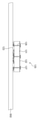
도 1 및 도 2를 참조하여, 반도체 패키지(1)는 배선 기판(100), 배선 기판(100) 상에 실장되는 제 1 및 제 2 반도체 칩들(200, 300), 및 배선 기판(100) 상에서 제 1 및 제 2 반도체 칩들(200, 300)을 덮는 몰딩막(400)을 포함할 수 있다.1 and 2 , a
배선 기판(100)이 제공될 수 있다. 배선 기판(100)은 코어층(core portion, 110), 코어층(110) 내부에 제공되는 인터포저 칩(120), 코어층(110)의 상부면에 배치되는 상부 주변부(upper buildup portion, 130), 및 코어층(110)의 하부면에 배치되는 하부 주변부(lower buildup portion, 140)을 포함할 수 있다.A
코어층(110)은 일 방향으로 연장될 수 있다. 코어층(110)은 평면적으로 일부분이 제거된 하나의 코어 패턴을 포함할 수 있다. 상기 일부분이 제거된 영역(CA)은 후술되는 인터포저 칩(120)이 배치되는 내장 영역(CA)에 해당할 수 있다. 내장 영역(CA)은 코어층(110)의 상부면 및 하부면을 연결하는 오픈 홀(open hole) 형태를 가질 수 있다. 본 발명의 실시예는 하나의 코어 패턴을 갖는 코어층(110)을 예시적으로 설명하고 있으나, 본 발명이 이에 한정되는 것은 아니다. 다른 실시예들에 따르면, 코어층(110)은 둘 혹은 그 이상의 코어 패턴을 포함할 수 있다. 즉, 배선 기판(100)은 평면적으로 이격된 복수의 코어 패턴들을 포함할 수 있다. 코어층(110)은 절연 물질을 포함할 수 있다. 예를 들어, 코어층(110)은 유리 섬유, 세라믹 판(ceramic plate), 에폭시 및 수지 중 어느 하나를 포함할 수 있다. 이와는 다르게, 코어층(110)은 스테인리스 스틸(stainless steel), 알루미늄(Al), 니켈(Ni), 마그네슘(Mg), 아연(Zn), 탄탈럼(Ta) 또는 이들의 조합 중에서 선택된 하나를 포함할 수 있다.The
코어층(110)은 코어 절연 패턴(112) 및 코어 절연 패턴(112) 내에 제공되는 배선 패턴인 코어 도전 패턴(114)을 포함할 수 있다. 예를 들어, 코어 절연 패턴(112)은 실리콘 산화물(SiO2)을 포함할 수 있다. 코어 도전 패턴(114)은 내장 영역(CA)으로부터 이격되어 배치될 수 있다. 일 예로, 코어 도전 패턴(114)은 내장 영역(CA)보다 코어층(110)의 외측에 배치될 수 있다. 코어 도전 패턴(114)은 상부 코어 패드들(115), 코어 배선들(116) 및 하부 코어 패드들(117)을 포함할 수 있다. 상부 코어 패드들(115)은 코어층(110)의 상부면 상에 제공될 수 있다. 상부 코어 패드들(115)은 후술되는 상부 주변부(130)와 전기적으로 연결될 수 있다. 하부 코어 패드들(117)은 코어층(110)의 하부에 제공될 수 있다. 하부 코어 패드들(117)은 후술되는 하부 주변부(140)와 전기적으로 연결될 수 있다. 상부 코어 패드들(115) 및 하부 코어 패드들(117)의 두께는 10um 내지 20um일 수 있다. 코어 배선들(116)은 상부 코어 패드들(115) 및 하부 코어 패드들(117)을 전기적으로 연결할 수 있다. 코어층(110)의 코어 절연 패턴(112)의 하부면 상에서 하부 코어 패드들(115)을 덮는 코어 보호층(119)을 더 포함할 수 있다. 다른 실시예들에 따르면, 코어 보호층(119)은 필요에 따라 제공되지 않을 수 있다. 즉, 이 경우 하부 코어 패드들(115)은 코어층(110)의 하부면 상에 노출될 수 있다.The
도 1에서는 복수로 적층된 코어 절연 패턴(112) 내에 매립되어 형성되는 코어 도전 패턴(114)의 구성을 도시하였으나, 본 발명이 이에 한정되는 것은 아니다. 도 3에 도시된 바와 같이, 코어층(110')의 코어 절연 패턴(112)은 하나의 층으로 제공될 수 있으며, 도 1에 도시된 코어 도전 패턴(114)을 대신하여 코어 절연 패턴(112)을 수직으로 관통하는 관통 전극들(114-1)이 제공될 수 있다. 관통 전극들(114-1)은 코어 전연 패턴(112)의 상부면으로부터 하부면까지 연장될 수 있다. 관통 전극들(114-1)의 상부면 상에는 상부 코어 패드들(115)이 접속될 수 있으며, 관통 전극들(114-1)의 하부면 상에는 하부 코어 패드들(117)이 접속될 수 있다. 이하 도 1 및 도 2의 실시예를 기준으로 계속 설명하도록 한다.Although FIG. 1 illustrates the configuration of the core
코어층(110)의 내장 영역(CA) 내에 인터포저 칩(120)이 제공될 수 있다. 내장 영역(CA)은 코어층(110)의 코어 패턴이 제거된 부분일 수 있다. 내장 영역(CA)은 코어층(110)의 상부면 및 하부면으로 노출될 수 있다. 즉, 내장 영역(CA)은 코어층(110)의 상부면으로부터 코어층(110)의 하부면을 향하여 연장된 관통 홀 형상을 가질 수 있다. 도시된 바와는 다르게, 내장 영역(CA)은 코어층(110)의 내부를 향하여 연장되는 리세스 형상을 가질 수 있다. 이 경우, 내장 영역(CA)의 바닥면은 코어 보호층(119)에 해당할 수 있다.The
인터포저 칩(120)은 베이스층(121), 베이스층(121) 상의 재배선층(123), 및 베이스층(121) 내의 비아들(126)을 포함할 수 있다.The
베이스층(121)은 실리콘(Si)을 포함할 수 있다. 베이스층(121)의 두께는 70um 내지 300um일 수 있다. 베이스층(121)의 하부면(121b)을 덮는 칩 보호층(122)이 제공될 수 있다. 칩 보호층(122)의 베이스층(121)의 하부의 일부일 수 있다. 예를 들어, 칩 보호층(122)은 베이스층(122)의 하부 일부가 산화되어 형성된 구성 요소일 수 있다.The
인터포저 칩(120)은 전면 및 후면을 가질 수 있다. 이하 본 명세서에서, 전면이라 함은, 인터포저 칩(120)의 배선 패턴들이 형성되는 면으로 정의되고, 후면이라 함은 상기 전면에 대향하는 반대면으로 정의될 수 있다. 예를 들어, 인터포저 칩(120)은 그의 전면에 제공되는 재배선층(123)을 포함할 수 있다. 재배선층(123)은 베이스층(121)의 상부면(121a) 상에 제공될 수 있다. 재배선층(123)은 인터포저 칩(120)의 전면에 배치되는 칩 도전 패턴(124) 및 칩 도전 패턴(124)을 덮는 칩 절연층(125)을 포함할 수 있다. 칩 도전 패턴(124) 중 칩 절연층(125)의 상부면 상으로 노출되는 칩 도전 패턴(124)의 일부는 상부 칩 패드들(124a, 124b, 124c)에 해당할 수 있다. 상부 칩 패드들(124a, 124b, 124c)의 노출된 면과 칩 절연층(125)의 일면은 공면(coplanar)을 이룰 수 있다. 칩 도전 패턴(124)은 금속과 같은 도전 물질을 이룰 수 있다. 예를 들어, 칩 도전 패턴(124)은 구리(Cu)를 포함할 수 있다. 칩 절연층(125)은 산화물을 포함할 수 있다. 예를 들어, 칩 절연층(125)은 실리콘 산화물(SiOx)를 포함할 수 있다.The
비아들(126)은 베이스층(121)을 수직으로 관통할 수 있다. 비아들(126)의 일단(126b)은 인터포저 칩(120)의 하부면 상에 노출될 수 있다. 이때, 비아들(126)의 하부면(126b)은 인터포저 칩(120)의 상기 후면(즉, 칩 보호층(122)의 하부면(121b)에 해당)과 공면(coplanar)을 이룰 수 있으며, 비아들(126)의 하부면(126b)과 인터포저 칩(120)의 상기 후면은 실질적으로 평탄(flat)할 수 있다. 비아들(126)의 다른 일단(126a)은 인터포저 칩(120)의 전면을 향하여 연장되어, 재배선층(123)과 접할 수 있다. 이때, 비아들(126)의 상부면(126a)은 베이스층(121)의 상부면(121a)과 동일한 레벨에 위치할 수 있으며, 비아들(126)의 다른 일단(126a)은 재배선층(123)의 하부면에 접할 수 있으며, 비아들(126)의 상부면(126a)은 재배선층(123)의 상기 하부면과 동일한 레벨에 배치될 수 있다. 즉, 재배선층(123)은 비아들(126)보다 위에 위치할 수 있다. 비아들(126)은 재배선층(123)의 칩 도전 패턴(124)에 접속될 수 있다. 비아들(126)의 폭은 50um 내지 150um일 수 있다.The
인터포저 칩(120)은 그의 후면(121b) 상에 제공되는 하부 칩 패드들(127)을 더 포함할 수 있다. 하부 칩 패드들(127)은 칩 보호층(122)의 하부면(121b) 상에 배치될 수 있다. 하부 칩 패드들(127)은 비아들(126)과 정렬될 수 있으며, 비아들(126)은 하부 칩 패드들(127)과 재배선층(123)의 칩 도전 패턴(124)을 연결시킬 수 있다. 하부 칩 패드들(127)은 그의 상부면 상에 시드막(128)이 제공될 수 있다. 시드막(128)은 하부 칩 패드들(127)과 비아들(126)의 사이 및 하부 칩 패드들(127)과 칩 보호층(122)의 사이에 개재될 수 있다.The
인터포저 칩(120)은 코어층(110)의 내장 영역(CA)의 내측면과 소정 거리로 이격되어 배치될 수 있으며, 코어층(110)의 내장 영역(CA)의 내측면으로 둘러쌀 수 있다. 즉, 평면적 관점에서 코어층(110)은 인터포저 칩(120)을 둘러싸는 형상을 가질 수 있다. 인터포저 칩(120)은 페이스-업(face-up)으로 제공될 수 있다. 즉, 인터포저 칩(120)은 재배선층(123)이 코어층(110)의 상부면을 향하도록 배치될 수 있다. 인터포저 칩(120)의 두께는 코어층(110)의 두께보다 작을 수 있다. 구체적으로, 인터포저 칩(120)의 두께는 코어층(110)의 두께와 같거나 작을 수 있다. 인터포저 칩(120)의 상부 칩 패드들(124a, 124b, 124c)의 상부면은 코어층(110)의 코어 절연 패턴(112)의 상부면보다 높은 레벨에 위치할 수 있다. 인터포저 칩(120)의 상부 칩 패드들(124a, 124b, 124c)은 코어층(110)의 상부 코어 패드들(117)과 동일한 레벨에 제공될 수 있다. 인터포저 칩(120)의 하부면은 코어층(110)의 하부면보다 높은 레벨에 위치할 수 있다. 예를 들어, 인터포저 칩(120)의 하부 칩 패드들(127)의 하부면은 코어 보호층(119)의 하부면보다 높을 레벨에 위치할 수 있다.The
다른 실시예들에서, 내장 영역(CA)이 코어층(110)의 내부를 향하여 연장되는 리세스 형상을 갖는 경우, 인터포저 칩(120)은 내장 영역(CA)의 바닥면 상에 안착될 수 있다. 이 경우, 인터포저 칩(120)은 접착제 또는 접착 필름 등을 이용하여 내장 영역(CA)의 바닥면에 접착될 수 있다.In other embodiments, when the embedded area CA has a recess shape extending toward the inside of the
인터포저 칩(120)은 별도의 직접 회로를 포함하지 않을 수 있다. 즉, 인터포저 칩(120)은 배선 기판(100)의 배선을 용이하게 하기 위하여 제공되는 구성 요소일 수 있다. 실리콘(Si)을 포함하는 인터포저 칩(120)은 반도체 집적(IC) 공정을 이용하여 재배선층(123)이 형성될 수 있으며, 이에 따라 인터포저 칩(120)의 재배선층(123)은 배선 밀도가 높을 수 있다. 이에 따라, 배선 기판(100)의 배선 자유도가 높을 수 있다. 더하여, 열 전도도가 높은 실리콘(Si) 및 수직으로 연장되는 비아들(126)에 의해 배선 기판(100) 상에 실장되는 제 1 반도체 칩(200) 및 제 2 반도체 칩(300)에서 발생하는 열이 하방으로 방출되기 용이할 수 있다. 즉, 열방출 효율이 높은 반도체 패키지(1)가 제공될 수 있다.The
이와는 다르게, 인터포저 칩(120)은 소정의 직접 회로를 포함할 수 있다. 이 경우, 상기 직접 회로는 인터포저 칩(120)의 전면에 형성될 수 있다. 상기 직접 회로는 접지(ground) 회로 또는 전력(power) 회로를 포함할 수 있다. 이와는 다르게, 상기 직접 회로는 메모리(memory) 회로, 로직(logic) 회로 또는 무선 주파수 직접 회로 등을 포함할 수 있다.Alternatively, the
내장 영역(CA) 내에서 코어층(110)과 인터포저 칩(120) 사이의 공간을 절연층(113)으로 채워질 수 있다. 절연층(113)은 인터포저 칩(120)의 아래 및 및 코어층(110)의 아래로 연장될 수 있다. 즉, 절연층(113)은 인터포저 칩(120)의 하부면 및 코어층(110)의 하부면을 덮을 수 있다. 그러나 도시된 바와는 다르게, 절연층(113)은 인터포저 칩(120)의 하부면 및 코어층(110)의 하부면을 노출시킬 수 있다. 절연층(113)은 절연성 고분자를 포함할 수 있다. 예를 들어, 절연층(113)은 에폭시 수지와 같은 열경화성 수지, 폴리이미드와 같은 열가소성 수지, 또는 이들에 무기 필러와 같은 보강재가 포함된 수지, 구체적으로 ABF, FR-4, BT, 수지 등을 포함할 수 있다. 또한, EMC와 같은 몰딩 물질 또는 PIE와 같은 감광성 재료가 사용될 수 있다.A space between the
상부 및 하부 저변부들(130, 140)은 각각 코어층(110)의 상부면 및 하부면을 덮을 수 있다. 상부 주변부(130)는 코어층(110)의 상부면 및 인터포저 칩(120)의 상부면을 덮을 수 있다. 하부 주변부(140)는 코어층(110)의 하부면 및 인터포저 칩(120)의 하부면을 덮을 수 있다.The upper and lower
상부 주변부(130)는 코어층(110)의 상부면 상에 순차적으로 적층되는 상부 절연 패턴들(132) 및 상부 배선 패턴들(134)을 포함할 수 있다. 상부 주변부(130)는 코어층(110)의 상부면 및 인터포저 칩(120)의 재배선층(123)을 덮을 수 있다. 하부 주변부(140)는 코어층(110)의 하부면 상에 순차적으로 적층되는 복수의 하부 절연 패턴들(142) 및 하부 배선 패턴들(144)을 포함할 수 있다. 하부 주변부(140)는 코어층(110)의 하부면 및 인터포저 칩(110)의 칩 절연층(125)을 덮을 수 있다. 상부 및 하부 절연 패턴들(132, 142)은 프리프레그(prepreg), ABF(Ajinomoto Build-up Film), FR-4 또는 BT(Bismaleimide Triazine)를 포함할 수 있다. 상부 및 하부 배선 패턴들(134, 144)은 회로 패턴(circuit pattern)을 포함할 수 있다. 상부 배선 패턴들(134)은 코어층(110)의 상부 코어 패드들(115) 및 인터포저 칩(120)의 상부 칩 패드들(124a, 124b, 124c)과 연결될 수 있다. 예를 들어, 상부 주변부(130)는 코어층(110)의 상부면 및 인터포저 칩(120)의 상부면과 접할 수 있으며, 상부 배선 패턴들(134)은 상부 코어 패드들(115) 및 상부 칩 패드들(124a, 124b, 124c)과 접할 수 있다. 하부 배선 패턴들(144)은 코어층(110)의 하부 코어 패드들(117) 및 인터포저 칩(120)의 하부 칩 패드들(127)과 연결될 수 있다. 예를 들어, 하부 주변부(140)는 절연층(113)의 하부면과 접할 수 있으며, 하부 배선 패턴들(144)은 절연층(113)을 관통하여 하부 칩 패드들(127) 및 하부 코어 패드들(117)과 접할 수 있다. 상부 및 하부 배선 패턴들(134, 144)은 구리(Cu), 알루미늄(Al), 은(Ag), 주석(Sn), 금(Au), 니켈(Ni), 납(Pb), 티타늄(Ti) 또는 이들의 조합 중에서 선택된 하나를 포함할 수 있다.The upper
하부 주변부(140) 아래에 외부 단자들(150)이 배치될 수 있다. 외부 단자들(150)은 하부 주변부(140)의 하부면에 제공될 수 있다. 예를 들어, 외부 단자들(140)은 하부 주변부(140)의 하부 절연 패턴들(142)을 관통하여 하부 배선 패턴들(144)에 접속될 수 있다. 또는, 외부 단자들(150)은 하부 주변부(140)의 하부면에 제공되는 기판 패드들 상에 배치될 수 있다. 이때, 상기 기판 패드들은 하부 주변부(140)의 하부 절연 패턴들(142)으로부터 노출되는 하부 배선 패턴들(144)의 일부이거나, 또는 하부 주변부(140)의 하부 절연 패턴들(142) 상에 배치되어 하부 배선 패턴들(144)과 연결되는 별도의 패드일 수 있다. 외부 단자들(150)은 하부 배선 패턴들(144)을 통해 인터포저 칩(120) 및 코어층(110)에 전기적으로 연결될 수 있다. 외부 단자들(150)은 솔더 볼(solder ball) 또는 솔더 범프(solder bump) 등을 포함할 수 있다.
배선 기판(100) 상에 제 1 반도체 칩(200) 및 제 2 반도체 칩(300)이 실장될 수 있다. 제 1 반도체 칩(200) 및 제 2 반도체 칩(300)은 서로 이격되어 배치될 수 있다. 제 1 반도체 칩(200) 및 제 2 반도체 칩(300)은 실리콘(Si)과 같은 반도체 물질을 포함할 수 있다. 제 1 반도체 칩(200) 및 제 2 반도체 칩(300)은 각각 제 1 회로층(210) 및 제 2 회로층(310)을 포함할 수 있다. 제 1 반도체 칩(200)의 제 1 회로층(210)은 로직 회로를 포함할 수 있다. 즉, 제 1 반도체 칩(200)은 로직 칩(logic chip)일 수 있다. 제 2 반도체 칩(300)의 제 2 회로층(310)은 메모리 회로를 포함할 수 있다. 즉, 제 2 반도체 칩(300)은 메모리 칩(memory chip)일 수 있다. 제 2 반도체 칩(300)은 복수로 제공될 수 있다. 이 경우, 복수의 제 2 반도체 칩(300)은 수직으로 적층되는 칩 스택(chip stack) 구조를 가질 수 있다. 제 1 반도체 칩(200) 및 제 2 반도체 칩(300)은 플립 칩(flip chip) 방식으로 배선 기판(100)에 실장될 수 있다. 예를 들어, 제 1 반도체 칩(200)의 제 1 회로층(210)의 일면 상에 배치되는 제 1 칩 패드들(220)에 제 1 칩 단자들(230)이 제공될 수 있다. 제 2 반도체 칩(300)의 제 2 회로층(310)의 일면 상에 배치되는 제 2 칩 패드들(320)에 제 2 칩 단자들(330)이 제공될 수 있다. 제 1 칩 단자들(230) 및 제 2 칩 단자들(330)은 상부 주변부(130)의 상부 배선 패턴들(134)에 접속될 수 있다. 예를 들어, 상부 배선 패턴들(134)의 일부는 상부 절연 패턴들(132)의 상부면 상으로 노출되는 패드일 수 있으며, 제 1 칩 단자들(230) 및 제 2 칩 단자들(330)은 상기 노출되는 상부 절연 패턴들(132)과 제 1 칩 패드들(220) 및 상기 노출되는 상부 절연 패턴들(132)과 제 2 칩 패드들(320)을 연결할 수 있다. 이때, 제 1 반도체 칩(200) 및 제 2 반도체 칩(300)은 인터포저 칩(120)을 통해 서로 연결될 수 있다. 예를 들어, 제 1 반도체 칩(200)은 상부 주변부(130)를 통해 인터포저 칩(120)의 재배선층(123)의 제 1 상부 칩 패드(124a)에 접속될 수 있다. 제 2 반도체 칩(300)은 상부 주변부(130)를 통해 인터포저 칩(120)의 재배선층(123)의 제 상부 칩 패드(124b)에 접속될 수 있다. 제 1 상부 칩 패드(124a) 및 제 2 상부 칩 패드(124b)는 재배선층(123) 내에서 서로 전기적으로 연결될 수 있다. 이에 따라, 제 1 반도체 칩(200)과 제 2 반도체 칩(300) 간의 chip to chip 연결이 형성될 수 있다. 제 1 반도체 칩(200)과 제 2 반도체 칩(300)이 배선 밀도가 높은 인터포저 칩(120)의 재배선층(123)을 이용하여 서로 연결됨에 따라, 제 1 반도체 칩(200)과 제 2 반도체 칩(300) 간의 전기적 연결 길이가 짧을 수 있으며, 전기적 특성이 향상된 반도체 패키지가 제공될 수 있다.The
제 1 반도체 칩(200)과 제 2 반도체 칩(300)을 서로 연결하는 제 1 및 제 2 상부 칩 패드들(124a, 124c)은 인터포저 칩(120)의 비아들(126)과 전기적으로 플로팅(floating)될 수 있다. 상부 칩 패드들(124a, 124b, 124c) 중 제 1 및 제 2 상부 칩 패드들(124a, 124b)을 제외한 제 3 상부 칩 패드들(124c)은 비아들(126)과 전기적으로 연결될 수 있다.The first and second
이와는 다르게, 제 1 반도체 칩(200)과 제 2 반도체 칩(300)을 서로 연결하는 제 1 및 제 2 상부 칩 패드들(124a, 124c)은 인터포저 칩(120)의 비아들(126)과 전기적으로 연결될 수 있다. 일 예로, 제 1 반도체 칩(200) 및 제 2 반도체 칩(300)은 하부 주변부(140), 비아들(126) 및 제 3 상부 칩 패드들(124c)을 통해 외부로부터 인가되는 전력 신호 또는 접지 신호를 전달받을 수 있다. 제 1 반도체 칩(200) 및 제 2 반도체 칩(300)에 제공되는 전력 신호 또는 접지 신호는 구동 신호가 전달되는 전기적 경로인 코어층(110)과는 별개로 분리되어 있는 인터포저 칩(120)을 통해 제 1 반도체 칩(200) 및 제 2 반도체 칩(300)에 전달될 수 있다. 이에 따라, 제 1 반도체 칩(200) 및 제 2 반도체 칩(300)에 전달되는 전력 신호 또는 접지 신호를 균일화하기 위하여 전력 회로 또는 접지 회로를 그룹화하기 용이할 수 있고, 구동 신호를 위한 배선 디자인 또는 전력 신호 및 접지 신호를 위한 배선 디자인이 용이하며, 배선 자유도가 높을 수 있다.Unlike this, the first and second
배선 기판(100) 상에 몰딩막(400)이 제공될 수 있다. 몰딩막(400)은 배선 기판(100)의 상부면 상에서 제 1 반도체 칩(200) 및 제 2 반도체 칩(300)을 덮을 수 있다. 몰딩막(400)은 절연 물질을 포함할 수 있다. 예를 들어, 몰딩막(400)은 에폭시 몰딩 컴파운드(EMC)를 포함할 수 있다.A
상기와 같이, 반도체 패키지(1)가 제공될 수 있다.As described above, the
도 4는 본 발명의 실시예들에 따른 반도체 패키지를 설명하기 위한 단면도이다. 이하의 실시예들에서는, 설명의 편의를 위하여 앞서 도 1 내지 도 3을 참조하여 설명한 것과 중복되는 기술적 특징에 대한 상세한 설명은 생략하고, 차이점에 대해 상세히 설명한다. 앞서 설명한 본 발명의 실시예들에 따른 반도체 장치와 동일한 구성에 대하여는 동일한 참조 번호가 제공될 수 있다.4 is a cross-sectional view illustrating a semiconductor package according to embodiments of the present invention. In the following embodiments, for convenience of description, detailed descriptions of technical features overlapping with those previously described with reference to FIGS. 1 to 3 will be omitted, and differences will be described in detail. The same reference numerals may be provided to the same components as those of the semiconductor devices according to the embodiments of the present invention described above.
도 4를 참조하여, 반도체 패키지(2)는 배선 기판(100), 배선 기판(100) 상에 실장되는 제 1 및 제 2 반도체 칩들(200, 300), 및 배선 기판(100) 상에서 제 1 및 제 2 반도체 칩들(200, 300)을 덮는 몰딩막(400)을 포함할 수 있다.Referring to FIG. 4 , a
배선 기판(100)이 제공될 수 있다. 배선 기판(100)은 인터포저 칩(120), 인터포저 칩(120) 상에 배치되는 상부 주변부(130), 및 인터포저 칩(120) 아래에 배치되는 하부 주변부(140)을 포함할 수 있다.A
인터포저 칩(120), 상부 주변부(130) 및 하부 주변부(140)는 도 1 내지 도 3을 참조하여 설명한 것과 실질적으로 동일 또는 유사할 수 있다.The
인터포저 칩(120)은 베이스층(121), 베이스층(121) 상의 재배선층(123), 및 베이스층(121) 내의 비아들(126)을 포함할 수 있다. 베이스층(121)은 실리콘(Si)을 포함할 수 있다. 재배선층(123)은 베이스층(121)의 상부면(121a) 상에 제공될 수 있다. 비아들(126)은 베이스층(121)을 수직으로 관통하여 재배선층(123)에 접속될 수 있다. 하부 칩 패드들(127)은 칩 보호층(122)의 하부면(121b) 상에 배치되어 비아들(126)과 정렬될 수 있다.The
상부 주변부(130)는 인터포저 칩(120) 상에 순차적으로 적층되는 상부 절연 패턴들(132) 및 상부 배선 패턴들(134)을 포함할 수 있다. 상부 배선 패턴들(134)은 인터포저 칩(120)의 상부 칩 패드들(124a, 124b, 124c)과 연결될 수 있다.The upper
하부 주변부(140)는 인터포저 칩(120) 아래에 순차적으로 적층되는 복수의 하부 절연 패턴들(142) 및 하부 배선 패턴들(144)을 포함할 수 있다. 하부 배선 패턴들(144)은 인터포저 칩(120)의 하부 칩 패드들(127)과 연결될 수 있다.The lower
절연층(113-1)은 하부 주변부(140)와 상부 주변부(130) 사이를 채울 수 있다. 절연층(113-1)은 하부 주변부(140)와 상부 주변부(130) 사이에서 인터포저 칩(120)을 매립할 수 있다. 즉, 인터포저 칩(120)은 평면적 관점에서 절연층(113-1)에 의해 둘러싸일 수 있다. 절연층(113-1)은 인터포저 칩(120)의 측면과 접할 수 있다. 절연층(113-1)의 일부는 인터포저 칩(120)의 하부면을 덮을 수 있다. 이에 따라, 인터포저 칩(120)의 하부 칩 패드들(127)은 노출되지 않을 수 있다. 절연층(113-1)은 에폭시 몰딩 컴파운드(EMC)와 같은 절연 물질을 포함할 수 있다. 또는, 절연층(113-1)은 절연성 고분자를 포함할 수 있다. 예를 들어, 절연층(113-1)은 에폭시 수지와 같은 열경화성 수지, 폴리이미드와 같은 열가소성 수지, 또는 이들에 무기 필러와 같은 보강재가 포함된 수지, 구체적으로 ABF, FR-4, BT, 수지 등을 포함할 수 있다. 또한, EMC와 같은 몰딩 물질 또는 PIE와 같은 감광성 재료가 사용될 수 있다.The insulating layer 113 - 1 may fill a space between the lower
절연층(113-1) 내부에 관통 전극(114-2)이 배치될 수 있다. 관통 전극(114-2)은 인터포저 칩(120)의 일측에서 절연층(113-1)을 수직으로 관통할 수 있다. 관통 전극(114-2)은 상부 주변부(130)를 향할수록 폭이 감소할 수 있다. 관통 전극(114-2)은 절연층(113-1)을 관통하여 절연층(113-1)의 상부면 상으로 노출될 수 있다. 상부 주변부(130)의 상부 배선 패턴들(134)은 상부 절연 패턴들(132)을 관통하여 관통 전극(114-2)의 상부면에 접할 수 있다. 관통 전극(114-2)은 절연층(113-1)을 관통하여 절연층(113-1)의 하부면 상으로 노출될 수 있다. 하부 주변부(140)의 하부 배선 패턴들(144)은 하부 절연 패턴들(142)을 관통하여 관통 전극(114-2)의 하부면에 접할 수 있다. 이때, 관통 전극(114-2)과 접하는 하부 배선 패턴들(144)의 일부는 관통 전극(114-2)과 일체로 이루어질 수 있다. 하부 배선 패턴들(144)은 또한 절연층(113-2)을 관통하여 하부 칩 패드들(127)에 접속될 수 있다.A through electrode 114 - 2 may be disposed inside the insulating layer 113 - 1 . The through electrode 114 - 2 may vertically penetrate the insulating layer 113 - 1 from one side of the
도 5는 본 발명의 실시예들에 따른 반도체 패키지를 설명하기 위한 단면도이다.5 is a cross-sectional view illustrating a semiconductor package according to embodiments of the present invention.
도 5를 참조하여, 반도체 패키지(3)는 배선 기판(100), 배선 기판(100) 상에 실장되는 제 1 및 제 2 반도체 칩들(200, 300), 및 배선 기판(100) 상에서 제 1 및 제 2 반도체 칩들(200, 300)을 덮는 몰딩막(400)을 포함할 수 있다.Referring to FIG. 5 , the
배선 기판(100), 제 1 및 제 2 반도체 칩들(200, 300) 및 몰딩막(400)은 도 1 내지 도 3을 참조하여 설명한 것과 실질적으로 동일 또는 유사할 수 있다. 예를 들어, 배선 기판(100)은 코어층(110), 코어층(110)의 내장 영역(CA) 내에 제공되는 인터포저 칩(120), 코어층(110) 상에 배치되는 상부 주변부(130), 및 코어층(110) 아래에 배치되는 하부 주변부(140)을 포함할 수 있다. 제 1 및 제 2 반도체 칩들(200, 300)은 배선 기판(100)의 상부 주변부(130) 상에 실장될 수 있다. 제 1 및 제 2 반도체 칩들(200, 300)은 상부 주변부(130) 및 인터포저 칩(120)의 재배선층(123)을 통해 서로 연결될 수 있다. 몰딩막(400)은 배선 기판(100) 상에서 제 1 및 제 2 반도체 칩들(200, 300)을 덮을 수 있다.The
반도체 패키지(3)은 몰딩막(400) 상에 제공되는 상부 패키지(500)를 더 포함할 수 있다. 즉, 반도체 패키지(3)는 패키지 온 패키지(package on package) 구조로 제공될 수 있다.The
상부 패키지(500)는 상부 기판(510), 상부 반도체 칩(520) 및 상부 몰딩막(530)을 포함할 수 있다.The
상부 기판(510)은 인쇄 회로 기판(PCB)일 수 있다. 또는 상부 기판(510)은 재배선 기판(redistribution layer)일 수 있다. 상부 기판(510)은 상부 기판(510)의 하부면 상에 제공되는 제 1 상부 기판 패드들(512) 및 상부 기판(510)의 상부면 상에 제공되는 제 2 상부 기판 패드들(514)을 가질 수 있다.The
상부 반도체 칩(520)은 상부 기판(510) 상에 실장될 수 있다. 예를 들어, 상부 반도체 칩(520)은 플립 칩(flip chip) 방식으로 상부 기판(510)에 실장될 수 있다. 상부 칩 패드들(522)과 제 2 상부 기판 패드들(514) 사이에 제공되는 제 3 칩 단자들(524)을 통해 상부 반도체 칩(520)이 상부 기판(510)에 실장될 수 있다. 상부 반도체 칩(520)은 메모리 칩(memory chip) 또는 로직 칩(logic chip)을 포함할 수 있다. 도 5에서는 하나의 상부 반도체 칩(520)이 제공되는 것을 도시하였으나, 본 발명이 이에 한정되는 것은 아니다. 상부 반도체 칩(520)은 복수로 제공될 수 있다. 이때, 복수의 상부 반도체 칩들(520)은 서로 적층되도록 제공되거나, 또는 상부 기판(510) 상에서 서로 수평적으로 이격되도록 제공될 수 있다.The
상부 몰딩막(530)이 상부 기판(510) 상에 제공될 수 있다. 상부 몰딩막(530)은 상부 기판 상에서 상부 반도체 칩(520)을 덮을 수 있다. 상부 몰딩막(530)은 에폭시 몰딩 컴파운드(EMC)와 같은 절연 물질을 포함할 수 있다.An
상부 패키지(500)는 배선 기판(100)에 실장될 수 있다. 상세하게는, 몰딩막(400) 내에 연결 단자들(410)이 제공될 수 있다. 연결 단자들(410)은 몰딩막(400)을 관통하여 상부 기판(510)의 제 1 상부 기판 패드(512)과 배선 기판(100)의 상부 주변부(130)의 상부 배선 패턴들(134)을 연결할 수 있다. 도 5에서는 연결 단자들(410)이 몰딩막(400)을 수직 관통하도록 형성되는 도전 포스트(post)인 것으로 도시하였으나, 본 발명이 이에 한정되는 것은 아니다. 연결 단자들(410)은 솔더 볼(solder ball) 또는 솔더 범프(solder bump)와 같은 솔더링 부재를 포함하거나, 제 1 상부 기판 패드(512)과 상부 배선 패턴들(134)을 기계적으로 연결할 수 있는 다양한 구조물을 포함할 수 있다. 상부 패키지(500)는 연결 단자(410) 및 배선 기판(100)을 통해 외부 단자(150)와 전기적으로 연결될 수 있다.The
상기와 같이 반도체 패키지(3)가 제공될 수 있다.As described above, the
도 6 내지 도 17은 본 발명의 실시예들에 따른 반도체 패키지의 제조 방법을 설명하기 위한 단면도들이다. 이중, 도 6 내지 도 11은 본 발명의 실시예들에 따른 인터포저 칩의 제조 방법을 설명하기 위한 단면도들이다.6 to 17 are cross-sectional views for explaining a method of manufacturing a semiconductor package according to embodiments of the present invention. Among them, FIGS. 6 to 11 are cross-sectional views for explaining a method of manufacturing an interposer chip according to embodiments of the present invention.
도 6을 참조하여, 베이스층(121)이 제공될 수 있다. 베이스층(121)은, 일 예로, 반도체 웨이퍼를 포함할 수 있다. 예를 들어, 베이스층(121)은 실리콘 웨이퍼일 수 있다. 베이스층(121)은 제 1 면(121a) 및 제 1 면(121a)에 대향하는 제 2 면(121c)을 가질 수 있다.Referring to FIG. 6 , a
베이스층(121)이 홀들(H)이 형성될 수 있다. 홀들(H)은 베이스층(121)의 제 1 면(121a) 상에 레이저 드릴링 등의 공정을 수행하여 형성될 수 있다. 또는, 베이스층(121)의 제 1 면(121a) 상에 마스크 패턴을 형성한 후, 상기 마스크 패턴을 식각 마스크로 이방성 식각 공정을 수행하여 홀들(H)이 형성될 수 있다. 홀들(H)은 베이스층(121)을 수직으로 완전히 관통하지는 않을 수 있다. 즉, 홀들(H)은 베이스층(121)의 제 2 면(121c)으로부터 이격되도록 형성될 수 있다.Holes H may be formed in the
도 7을 참조하여, 베이스층(121) 내부에 비아들(126)이 형성될 수 있다. 예를 들어, 베이스층(121)의 제 1 면(121a) 상에 도전 물질을 도포 또는 증착할 수 있다. 이때, 상기 도전 물질은 베이스층(121)의 홀들(H)을 채울 수 있다. 이후, 베이스층(121)의 제 1 면 (121a) 상에 위치하는 상기 도전 물질의 일부를 제거할 수 있으며, 상기 도전 물질은 홀들(H) 내에만 잔여할 수 있다.Referring to FIG. 7 , vias 126 may be formed in the
도 8을 참조하여, 베이스층(121)의 제 1 면(121a) 상에 재배선층(123)이 형성될 수 있다. 예를 들어, 베이스층(121)의 제 1 면(121a) 상에 실리콘 산화물과 같은 절연층을 형성한 후, 상기 절연층을 패터닝하여 칩 절연층(125)의 일부가 형성될 수 있다. 칩 절연층(125)에 의해 비아들(126)이 노출될 수 있다. 칩 절연층(125)의 상면 상에 도전츠응ㄹ 형성한 후, 상기 도전층을 패터닝하여 칩 도전 패턴(124)이 형성될 수 있다. 칩 도전 패턴(124)은 비아들(126)과 전기적으로 연결될 수 있다. 상기와 같이 절연층의 형성 및 패터닝 공정과 도전층의 형성 및 패터닝 공정을 반복하여 재배선층(123)이 형성될 수 있다.Referring to FIG. 8 , a
도 9를 참조하여, 베이스층(121)의 일부가 제거될 수 있다. 상세하게는, 비아들(126)이 노출되도록, 베이스층(121)이 박형화될 수 있다. 예를 들어, 베이스층(121)의 제 2 면(121c) 상에 화학 기계적 연마 공정(CMP) 또는 그라인딩 공정이 수행될 수 있다. 상기 박형화 공정이 수행되어 나타나는 베이스층(121)의 제 3 면(121b)은 비아들(126)의 일단과 공면을 이룰 수 있다. 즉, 베이스층(121)의 제 3 면(121b)과 비아들(126)의 일단은 실질적으로 평탄(flat)할 수 있다.Referring to FIG. 9 , a portion of the
도 10을 참조하여, 베이스층(121)의 제 3 면(121b) 측에 칩 보호층(122)을 형성할 수 있다. 상세하게는, 베이스층(121)의 노출되는 제 3 면(121b) 상에 산화 공정 또는 질화 공정이 수행될 수 있다. 이에 따라, 제 3 면(121b) 측의 베이스층(121)의 일부가 산화 또는 질화되어 칩 보호층(122)이 형성될 수 있다. 칩 보호층(122)의 상면은 비아들(126)의 일단과 공면을 이룰 수 있다.Referring to FIG. 10 , a
칩 보호층(122) 상에 하부 칩 패드들(127)이 형성될 수 있다. 상세하게는, 칩 보호층(122) 상에 시드막(128)이 형성될 수 있다. 시드막(128)은 칩 보호층(122)의 상면 및 비아들(126)의 상면들을 덮을 수 있다. 시드막(128) 상에 마스크 패턴(MP)이 형성될 수 있다. 마스크 패턴(MP)의 개구들은 비아들(126)과 오버랩될 수 있다. 이후, 시드막(128)을 시드로 도금 공정이 수행되어, 마스크 패턴(MP)의 상기 개구들을 채우는 하부 칩 패드들(127)이 형성될 수 있다. 하부 칩 패드들(127)은 각각 비아들(126) 상에 형성될 수 있다.
도 11을 참조하여, 마스크 패턴(MP)이 제거될 수 있다. 이후, 하부 칩 패드들(127)을 식각 마스크로 시드막(128)이 패터닝될 수 있다. 이에 따라, 시드막(128)은 하부 칩 패드들(127)과 칩 보호층(122) 사이 및 하부 칩 패드들(127)과 비아들(126) 사이에 잔여하도록 형성될 수 있다.Referring to FIG. 11 , the mask pattern MP may be removed. Thereafter, the
상기와 같이 인터포저 칩(120)이 형성될 수 있다.The
도 6 내지 도 11에서는 베이스층(121)에 하나의 인터포저 칩(120)이 형성되는 것을 도시하였으나, 본 발명이 이에 한정되는 것은 아니다. 실시예들에 따르면 하나의 베이스층(121)에 복수의 인터포저 칩(120)이 형성될 수 있으며, 이 경우 인터포저 칩들(120)의 형성 후 베이스층(121)에 쏘잉(sawing) 공정을 수행하여 인터포저 칩들(120)이 분리될 수 있다.6 to 11 illustrate that one
이하, 반도체 패키지의 제조 방법을 계속 설명하도록 한다.Hereinafter, a method of manufacturing a semiconductor package will be continuously described.
도 12를 참조하여, 코어층(110)이 제공될 수 있다. 코어층(110)은 코어 절연 패턴(112) 및 코어 절연 패턴(112) 내에 형성되는 코어 도전 패턴(114)을 포함할 수 있다. 코어 도전 패턴(114)은 상부 코어 패드들(115), 코어 배선들(116) 및 하부 코어 패드들(117)을 포함할 수 있다. 코어 절연 패턴(112)의 하부면 상에 코어 보호층(119)이 형성될 수 있다. 예를 들어, 코어 절연 패턴(112)의 하부면 상에 절연 물질을 도포하여 코어 보호층(119)이 형성될 수 있다.Referring to FIG. 12 , a
코어층(110)의 하부면 상에 제 1 캐리어 기판(900)이 부착될 수 있다. 제 1 캐리어 기판(900)은 유리 또는 폴리머를 포함한 절연 기판이거나, 금속을 포함하는 도전성 기판일 수 있다. 제 1 캐리어 기판(900)은 그의 상면 상에 제공되는 접착 부재(미도시)를 통해 코어층(110)의 코어 보호층(119)의 하면과 접착될 수 있다. 일 예로, 접착 부재(미도시)는 접착 테이프를 포함할 수 있다A
코어층(110) 상에는 보호층(910)이 형성될 수 있다.A
도 13을 참조하여, 코어층(110) 내에 내장 영역(CA)이 형성될 수 있다. 내장 영역(CA)은 코어층(110)을 관통하도록 코어층(110)의 일부 영역을 제거하여 형성될 수 있다. 예를 들어, 내장 영역(CA)을 형성하는 공정은 드릴링(drilling) 공정, 레이저 어블레이션(laser ablation) 공정 또는 레이저 커팅(laser cutting)과 같은 식각 공정을 통해 수행될 수 있다. 상기 제거되는 코어층(110)의 일부 영역은 후순되는 공정에서 인터포저 기판(120)이 제공되는 공간일 수 있다.Referring to FIG. 13 , an embedded region CA may be formed in the
도 14를 참조하여, 도 13의 결과물에서 제 1 캐리어 기판(900) 및 보호층(910)이 제거될 수 있다.Referring to FIG. 14 , the
제 2 캐리어 기판(920)이 코어층(110)에 부착될 수 있다. 제 2 캐리어 기판(920)은 유리 또는 폴리머를 포함한 절연 기판이거나, 금속을 포함하는 도전성 기판일 수 있다. 제 2 캐리어 기판(920)은 그의 상면 상에 제공되는 접착 부재(미도시)를 통해 코어층(110)과 접착될 수 있다. 일 예로, 접착 부재(미도시)는 접착 테이프를 포함할 수 있다. 이때, 코어층(110)은 상부 코어 패드들(115)이 제 2 캐리어 기판(920)을 향하도록 제 2 캐리어 기판(920)에 부착될 수 있다.A
인터포저 칩(120)이 제 2 캐리어 기판(920) 상에 제공될 수 있다. 인터포저 칩(120)은 코어층(110)의 내장 영역(CA) 내에 배치될 수 있다. 인터포저 칩(120)은 제 2 캐리어 기판(920) 상에 부착될 수 있다. 이때, 인터포저 칩(120)은 재배선층(123)이 제 2 캐리어 기판(920)을 향하도록 제 2 캐리어 기판(920)에 부착될 수 있다. 이에 따라, 인터포저 칩(120)의 재배선층(123)의 일면은 코어층(110)의 코어 절연 패턴(112)의 하면보다 낮은 레벨에 위치하고, 코어층(110)의 상부 코어 패드들(115)의 일면과 동일한 레벨에 위치할 수 있다.The
도 15를 참조하여, 절연층(113)이 제 2 캐리어 기판(920) 상에 형성될 수 있다. 절연층(113)은 코어층(110)과 인터포저 칩(120) 사이를 채울 수 있다. 예를 들면, 코어층(110)과 인터포저 칩(120) 사이에 절연 부재를 주입한 후, 상기 절연 부재를 경화시켜 절연층(113)이 형성될 수 있다. 실시예들에 따르면, 상기 절연 부재는 인터포저 칩(120)을 덮도록 형성될 수 있다. 이에 따라 인터포저 칩(120)의 하부 칩 패드들(127)은 노출되지 않을 수 있다. 또한, 상기 절연 부재의 일부는 코어층(110)의 상부면을 덮도록 제공될 수 있다. 이와는 다르게, 절연층(113)은 코어층(110)의 상부면을 덮지 않도록 형성되거나, 또는 인터포저 칩(110)의 상부면을 덮지 않도록 형성될 수 있다.Referring to FIG. 15 , an insulating
도 16을 참조하여, 제 3 캐리어 기판(930)이 절연층(113)에 부착될 수 있다. 제 3 캐리어 기판(930)은 유리 또는 폴리머를 포함한 절연 기판이거나, 금속을 포함하는 도전성 기판일 수 있다. 제 3 캐리어 기판(930)은 그의 상면 상에 제공되는 접착 부재(미도시)를 통해 절연층(113)과 접착될 수 있다. 일 예로, 접착 부재(미도시)는 접착 테이프를 포함할 수 있다. 이후 제 2 캐리어 기판(920)이 제거될 수 있다.Referring to FIG. 16 , a
제 2 캐리어 기판(920)이 제거되어 노출되는 코어층(110)의 상면 및 인터포저 칩(120)의 상면 상에 상부 주변부(130)가 형성될 수 있다. 예를 들어, 상부 절연 패턴들(132) 및 상부 배선 패턴들(134)이 코어층(110)의 상기 상면 및 인터포저 칩(120)의 상기 상면 상에 형성되어, 상부 주변부(130)가 형성될 수 있다. 코어층(110)의 상기 상면 및 인터포저 칩(120)의 상기 상면 상에 실리콘 산화물과 같은 절연층을 형성한 후, 상기 절연층을 패터닝하여 상부 절연 패턴들(132)의 일부가 형성될 수 있다. 상부 절연 패턴들(132)에 의해 인터포저 칩(120)의 재배선층(123)의 상부 칩 패드들(124a, 124b, 124c, 도 2 참조) 및 코어층(110)의 상부 코어 패드들(115)이 노출될 수 있다. 상부 절연 패턴들(132)의 상면 상에 도전층을 형성한 후, 상기 도전층을 패터닝하여 상부 배선 패턴들(134)이 형성될 수 있다. 상부 배선 패턴들(134)은 상부 칩 패드들(124a, 124b, 124c, 도 2 참조) 및 상부 코어 패드들(115) 중 어느 하나와 전기적으로 연결될 수 있다. 상부 배선 패턴들(134)의 상면 상에 절연층을 형성한 후, 상기 절연층을 패터닝하여 상부 절연 패턴들(132)의 다른 일부가 형성될 수 있다. 이때, 상부 배선 패턴들(134)의 일부는 상부 절연 패턴들(132) 상으로 노출될 수 있다.The upper
도 17을 참조하여, 제 4 캐리어 기판(940)이 상부 주변부(130)에 부착될 수 있다. 제 4 캐리어 기판(940)은 유리 또는 폴리머를 포함한 절연 기판이거나, 금속을 포함하는 도전성 기판일 수 있다. 제 4 캐리어 기판(940)은 그의 상면 상에 제공되는 접착 부재(미도시)를 통해 상부 주변부(130)과 접착될 수 있다. 일 예로, 접착 부재(미도시)는 접착 테이프를 포함할 수 있다. 이후 제 3 캐리어 기판(930)이 제거될 수 있다.Referring to FIG. 17 , a
제 3 캐리어 기판(930)이 제거되어 노출되는 코어층(110)의 하면 및 인터포저 칩(120)의 하면 상에 하부 주변부(140)가 형성될 수 있다. 예를 들어, 하부 절연 패턴들(142) 및 하부 배선 패턴들(144)이 코어층(110)의 상기 하면 및 인터포저 칩(120)의 상기 하면 상에 형성되어, 하부 주변부(140)가 형성될 수 있다. 인터포저 칩(120)의 하부 칩 패드들(127) 및 코어층(110)의 하부 코어 패드들(117)이 노출되도록 절연층(113)을 패터닝한 후, 절연층(113)의 하면 상에 도전층을 형성하고, 상기 도전층을 패터닝하여 하부 배선 패턴들(144)의 일부가 형성될 수 있다. 하부 배선 패턴들(144)은 하부 칩 패드들(127) 및 하부 코어 패드들(117) 중 어느 하나와 전기적으로 연결될 수 있다. 하부 배선 패턴들(144)의 하면 상에 절연층을 형성한 후, 상기 절연층을 패터닝하여 하부 절연 패턴들(142)의 다른 일부가 형성될 수 있다. 이때, 하부 배선 패턴들(144)의 일부는 하부 절연 패턴들(142) 상으로 노출될 수 있다.A lower
이후, 제 4 캐리어 기판(940)이 제거되어 배선 기판(100)이 형성될 수 있다.Thereafter, the
도 1을 다시 참조하여, 배선 기판(100) 상에 제 1 및 제 2 반도체 칩들(200, 300)이 실장될 수 있다. 제 1 및 제 2 반도체 칩들(200, 300)은 플립 칩(flip chip) 방식으로 실장될 수 있다.Referring back to FIG. 1 , the first and
배선 기판(100) 상에 몰딩막(400)이 형성될 수 있다. 예를 들어, 배선 기판(100) 상에 제 1 및 제 2 반도체 칩들(200, 300)을 덮도록 절연 물질을 도포한 후, 상기 절연 물질을 경화시켜 몰딩막(400)이 형성될 수 있다.A
배선 기판(100)의 하부면 상에 외부 단자들(150)이 제공될 수 있다. 외부 단자들(150)은 하부 절연 패턴들(142)을 패터닝하여 노출되는 하부 배선 패턴들(144)의 일면 상에 솔더 볼 또는 솔더 범프와 같은 솔더 부재를 제공하여 형성될 수 있다.
상기와 같이 반도체 패키지(1)가 형성될 수 있다.The
도 12 내지 도 17에서는 하나의 배선 기판(100)에 하나의 반도체 패키지가 형성되는 것을 도시하였으나, 본 발명이 이에 한정되는 것은 아니다. 실시예들에 따르면 하나의 배선 기판(100)에 복수의 반도체 패키지(1)가 형성될 수 있으며, 이 경우 반도체 패키지들(1)의 형성 후 배선 기판(100) 및 몰딩막(400)에 쏘잉(sawing) 공정을 수행하여 반도체 패키지들(1)이 분리될 수 있다.12 to 17 illustrate that one semiconductor package is formed on one
도 18 내지 도 21은 본 발명의 실시예들에 따른 반도체 패키지의 제조 방법을 설명하기 위한 단면도들이다.18 to 21 are cross-sectional views for explaining a method of manufacturing a semiconductor package according to embodiments of the present invention.
도 18을 참조하여, 인터포저 칩(120)이 제 5 캐리어 기판(950) 상에 제공될 수 있다. 인터포저 칩(120)은 제 5 캐리어 기판(950) 상에 부착ㄷ힐 수 있다. 이때, 인터포저 칩(120)은 재배선층(123)이 제 5 캐리어 기판(950)을 향하도록 제 5 캐리어 기판(950)에 부착될 수 있다.Referring to FIG. 18 , the
도 19를 참조하여, 제 5 캐리어 기판(950) 상에 절연층(113-1)이 형성될 수 있다. 절연층(113-1)은 제 5 캐리어 기판(950) 상에 절연 물질을 도포하여 형성될 수 있다. 상기 절연 물질은 제 5 캐리어 기판(950) 상에서 인터포저 칩(120)을 덮도록 도포될 수 있다. 절연층(113-1)은 인터포저 칩(120)의 측면을 덮고, 인터포저 칩(120)의 상부면(즉, 칩 보호층(122)의 상부면 및 하부 칩 패드들(127)의 상면)을 덮을 수 있다. 상기 절연 물질은 에폭시계 몰딩 컴파운드(EMC)와 같은 절연성 폴리머를 포함할 수 있다.Referring to FIG. 19 , an insulating layer 113 - 1 may be formed on the
도 21을 참조하여, 절연층(113-1)에 관통 전극들(114-2)이 형성될 수 있다. 예를 들어, 절연층(113-1)에 절연층(113-1)을 수직으로 관통하는 비아 홀들(VH)을 형성한 후, 비아 홀들(VH)에 도전 물질을 채워 관통 전극들(114-2)이 형성될 수 있다. 비아 홀들(VJ) 내에 상기 도전 물질을 채울 때, 상기 도전 물질은 절연층(113-1)의 상면을 덮도록 절연층(113-2) 상에 도포될 수 있으며, 절연층(113-1) 상의 상기 도전 물질은 패터닝되어 하부 주변부(140)의 하부 배선 패턴들(144)의 일부를 형성할 수 있다.Referring to FIG. 21 , through electrodes 114 - 2 may be formed in the insulating layer 113 - 1 . For example, after forming via-holes VH vertically penetrating the insulating layer 113-1 in the insulating layer 113-1, the via-holes VH are filled with a conductive material to form the through-electrodes 114- 2) can be formed. When the conductive material is filled in the via holes VJ, the conductive material may be applied on the insulating layer 113-2 to cover the upper surface of the insulating layer 113-1, and the insulating layer 113-1. The conductive material on the upper portion may be patterned to form a portion of the
절연층(113-1) 상에 하부 주변부(140)가 형성될 수 있다. 예를 들어, 하부 절연 패턴들(142) 및 하부 배선 패턴들(144)이 절연층(113-1)의 상부면 상에 형성되어, 하부 주변부(140)가 형성될 수 있다. 인터포저 칩(120)의 하부 칩 패드들(127) 및 관통 전극들(114-2)이 노출되도록 절연층(113-1)을 패터닝한 후, 절연층(113-1)의 상부면 상에 도전층을 형성하고, 상기 도전층을 패터닝하여 하부 배선 패턴들(144)의 일부가 형성될 수 있다. 하부 배선 패턴들(144)은 하부 칩 패드들(127) 및 관통 전극(114-2) 중 어느 하나와 전기적으로 연결될 수 있다. 하부 배선 패턴들(144)의 하면 상에 절연층을 형성한 후, 상기 절연층을 패터닝하여 하부 절연 패턴들(142)의 다른 일부가 형성될 수 있다. 이때, 하부 배선 패턴들(144)의 일부는 하부 절연 패턴들(142) 상으로 노출될 수 있다.A lower
도 21을 참조하여, 제 5 캐리어 기판(950)이 제거되어 노출되는 절연층(113-1)의 일면 및 인터포저 칩(120)의 일면 상에 상부 주변부(130)가 형성될 수 있다. 예를 들어, 상부 절연 패턴들(132) 및 상부 배선 패턴들(134)이 절연층(113-1)의 상기 일면 및 인터포저 칩(120)의 상기 일면 상에 형성되어, 상부 주변부(130)가 형성될 수 있다. 절연층(113-1)의 상기 일면 및 인터포저 칩(120)의 상기 일면 상에 실리콘 산화물과 같은 절연층을 형성한 후, 상기 절연층을 패터닝하여 상부 절연 패턴들(132)의 일부가 형성될 수 있다. 상부 절연 패턴들(132)에 의해 인터포저 칩(120)의 재배선층(123)의 상부 칩 패드들(124a, 124b, 124c, 도 2 참조) 및 절연층(113-1) 내의 관통 전극들(114-2)이 노출될 수 있다. 상부 절연 패턴들(132)의 상면 상에 도전층을 형성한 후, 상기 도전층을 패터닝하여 상부 배선 패턴들(134)이 형성될 수 있다. 상부 배선 패턴들(134)은 상부 칩 패드들(124a, 124b, 124c, 도 2 참조) 및 관통 전극들(114-2) 중 어느 하나와 전기적으로 연결될 수 있다. 상부 배선 패턴들(134)의 상면 상에 절연층을 형성한 후, 상기 절연층을 패터닝하여 상부 절연 패턴들(132)의 다른 일부가 형성될 수 있다. 이때, 상부 배선 패턴들(134)의 일부는 상부 절연 패턴들(132) 상으로 노출될 수 있다. 상기와 같이 도 4를 참조하여 설명한 배선 기판(100)이 형성될 수 있다.Referring to FIG. 21 , an upper
이후, 도 1을 참조하여 설명한 것과 동일 또는 유사한 공정이 수행될 수 있다. 예를 들어, 도 4에 도시된 바와 같이, 배선 기판(100) 상에 제 1 및 제 2 반도체 칩들(200, 300)이 실장될 수 있다. 배선 기판(100) 상에 제 1 및 제 2 반도체 칩들(200, 300)을 덮는 몰딩막(400)이 형성될 수 있다. 배선 기판(100)의 하부면 상에 외부 단자들(150)이 제공될 수 있다.Thereafter, the same or similar process as described with reference to FIG. 1 may be performed. For example, as shown in FIG. 4 , the first and
상기와 같이 도 4를 참조하여 설명한 반도체 패키지(2)가 형성될 수 있다.As described above, the
이상, 첨부된 도면들을 참조하여 본 발명의 실시예들을 설명하였지만, 본 발명이 속하는 기술분야에서 통상의 지식을 가진 자는 본 발명이 그 기술적 사상이나 필수적인 특징을 변경하지 않고서 다른 구체적인 형태로 실시될 수 있다는 것을 이해할 수 있을 것이다. 그러므로 이상에서 기술한 실시예들은 모든 면에서 예시적인 것이며 한정적이 아닌 것으로 이해해야만 한다.In the above, embodiments of the present invention have been described with reference to the accompanying drawings, but those of ordinary skill in the art to which the present invention pertains can practice the present invention in other specific forms without changing its technical spirit or essential features. You will understand that there is Therefore, it should be understood that the embodiments described above are illustrative in all respects and not restrictive.
100: 배선 기판
110: 코어층
120: 인터포저 칩
130: 상부 주변부
140: 하부 주변부
200, 300: 반도체 칩
400: 몰딩막100: wiring board 110: core layer
120: interposer chip 130: upper periphery
140: lower
400: molding film
Claims (20)
상기 기판 상에 실장되는 제 1 반도체 칩 및 제 2 반도체 칩; 및
상기 기판 아래에 제공되는 외부 단자들을 포함하되,
상기 기판은:
코어층;
상기 코어층의 상부면 및 하부면 상에 각각 제공되되 절연 패턴 및 배선 패턴을 각각 포함하는 제 1 주변부 및 제 2 주변부; 및
상기 코어층 내에 형성된 내장 영역에 제공되고, 상기 제 1 주변부 및 상기 제 2 주변부에 전기적으로 연결되는 인터포저 칩을 포함하고,
상기 인터포저 칩은:
베이스층;
상기 베이스층의 제 1 면 상에 제공되는 재배선층; 및
상기 베이스층을 관통하여 상기 재배선층에 연결되고, 상기 베이스층의 제 2 면 상으로 노출되는 비아를 포함하고,
상기 재배선층은 상기 제 1 주변부의 배선 패턴과 연결되고, 상기 비아는 상기 제 2 주변부의 배선 패턴과 연결되는 반도체 패키지.
Board;
a first semiconductor chip and a second semiconductor chip mounted on the substrate; and
Including external terminals provided under the substrate,
The substrate is:
core layer;
a first peripheral portion and a second peripheral portion respectively provided on an upper surface and a lower surface of the core layer and including an insulating pattern and a wiring pattern, respectively; and
an interposer chip provided in an embedded region formed in the core layer and electrically connected to the first periphery and the second periphery;
The interposer chip is:
base layer;
a redistribution layer provided on the first surface of the base layer; and
a via passing through the base layer and connected to the redistribution layer and exposed on a second surface of the base layer;
The redistribution layer is connected to the wiring pattern of the first peripheral portion, and the via is connected to the wiring pattern of the second peripheral portion.
상기 인터포저 칩은:
상기 베이스층의 상기 제 2 면을 덮고, 상기 비아를 노출시키는 보호층; 및
상기 보호층의 일면 상에 제공되어, 상기 비아와 상기 제 2 주변부의 상기 배선 패턴을 연결하는 패드를 더 포함하는 반도체 패키지.The method of claim 1,
The interposer chip is:
a protective layer covering the second surface of the base layer and exposing the via; and
and a pad provided on one surface of the protective layer to connect the via and the wiring pattern of the second peripheral portion.
상기 재배선층은 상기 비아 상에 위치하고,
상기 비아의 상부면은 상기 베이스층의 상기 제 1 면과 동일한 레벨에 배치되는 반도체 패키지.The method of claim 1,
the redistribution layer is located on the via;
and an upper surface of the via is disposed at the same level as the first surface of the base layer.
상기 인터포저 칩의 상기 재배선층의 상부면은 상기 코어층의 상부면과 동일한 레벨에 위치하는 반도체 패키지.The method of claim 1,
and an upper surface of the redistribution layer of the interposer chip is positioned at the same level as an upper surface of the core layer.
상기 내장 영역은 상기 코어층을 수직으로 관통하도록 형성되는 오픈 홀의 형상을 갖되,
상기 인터포저 칩은 상기 내장 영역의 내측벽으로부터 이격되는 반도체 패키지.The method of claim 1,
The embedded region has a shape of an open hole formed to vertically penetrate the core layer,
The interposer chip is spaced apart from an inner wall of the embedded region.
상기 내장 영역의 상기 내측벽과 상기 인터포저 칩 사이의 갭을 채우고, 상기 인터포저 칩의 하부면을 덮는 절연층을 더 포함하되,
상기 제 2 주변부의 상기 배선 패턴은 상기 절연층을 관통하여 상기 비아와 접속되는 반도체 패키지.6. The method of claim 5,
an insulating layer filling a gap between the inner wall of the embedded region and the interposer chip and covering a lower surface of the interposer chip,
The wiring pattern of the second peripheral portion penetrates the insulating layer and is connected to the via.
상기 코어층은 상기 내장 영역으로부터 이격되고, 상기 제 1 주변부 및 상기 제 2 주변부를 전기적으로 연결하는 코어 도전 패턴들을 더 포함하는 반도체 패키지.6. The method of claim 5,
The core layer may further include core conductive patterns spaced apart from the embedded region and electrically connecting the first peripheral portion and the second peripheral portion.
상기 코어층은 상기 인터포저 칩을 둘러싸되, 상기 인터포저 칩의 측면과 접하고,
상기 코어층은 상기 코어층을 수직으로 관통하여 상기 제 1 주변부의 상기 배선 패턴 및 상기 제 2 주변부의 상기 배선 패턴을 직접적으로 연결하는 관통 전극을 더 포함하는 반도체 패키지.The method of claim 1,
The core layer surrounds the interposer chip, and is in contact with a side surface of the interposer chip,
The core layer further includes a through electrode penetrating the core layer vertically to directly connect the wiring pattern of the first periphery and the wiring pattern of the second periphery.
상기 제 1 및 제 2 반도체 칩들은 상기 제 1 주변부 및 상기 인터포저 칩을 통해 서로 전기적으로 연결되는 반도체 패키지.The method of claim 1,
The first and second semiconductor chips are electrically connected to each other through the first peripheral portion and the interposer chip.
상기 실장 영역은 상기 코어층의 상부에 형성되고,
상기 인터포저 칩은 상기 코어층의 바닥면 상에 배치되며,
상기 제 2 주변부의 상비기 배선 패턴은 상기 코어층을 관통하여 상기 인터포저 칩의 상기 비아와 접하는 반도체 패키지.The method of claim 1,
The mounting region is formed on the core layer,
The interposer chip is disposed on the bottom surface of the core layer,
The standby interconnection pattern of the second peripheral portion penetrates the core layer and contacts the via of the interposer chip.
상기 인터포저 칩의 하부면은 상기 코어층의 하부면보다 높은 레벨에 위치하는 반도체 패키지.The method of claim 1,
A lower surface of the interposer chip is positioned at a higher level than a lower surface of the core layer.
상기 인터포저 칩의 베이스층은 실리콘(Si)을 포함하는 반도체 패키지.The method of claim 1,
The base layer of the interposer chip is a semiconductor package including silicon (Si).
상기 제 1 주변부 상에서 상기 제 1 및 제 2 반도체 칩들을 덮는 몰딩막;
상기 몰딩막 상에 제공되는 재배선 기판; 및
상기 몰딩막을 관통하여 상기 재배선 기판을 상기 제 1 주변부에 연결하는 연결 단자를 더 포함하는 반도체 패키지.
The method of claim 1,
a molding layer covering the first and second semiconductor chips on the first peripheral portion;
a redistribution substrate provided on the molding layer; and
and a connection terminal passing through the molding layer to connect the redistribution substrate to the first peripheral portion.
상기 제 1 배선층과 상기 제 2 배선층 사이의 인터포저 칩;
상기 제 1 배선층과 상기 제 1 배선층 사이에 제공되고, 상기 인터포저 칩을 둘러싸는 절연층;
상기 제 1 배선층과 상기 제 1 2 배선층 사이에서 상기 인터포저 칩과 이격되어 배치되고, 상기 제 1 배선층과 상기 제 2 배선층을 연결하는 도전부;
상기 제 2 배선층 상에 실장되는 제 1 반도체 칩 및 제 2 반도체 칩;
상기 제 2 배선층 상에서 제 1 및 제 2 반도체 칩들을 덮는 몰딩막; 및
상기 제 1 배선층 아래에 제공되는 외부 단자들을 포함하되,
상기 인터포저 칩은:
베이스층;
상기 베이스층 상에서 상기 제 2 배선층에 접속되는 재배선층; 및
상기 베이스층 내에 제공되고, 상기 재배선층과 상기 제 1 배선층을 연결하는 비아를 포함하고,
상기 제 1 및 제 2 반도체 칩들은 상기 인터포저 칩을 통해 서로 전기적으로 연결되는 반도체 패키지.
a first wiring layer and a second wiring layer on the first wiring layer;
an interposer chip between the first wiring layer and the second wiring layer;
an insulating layer provided between the first wiring layer and the first wiring layer and surrounding the interposer chip;
a conductive part disposed between the first wiring layer and the first second wiring layer to be spaced apart from the interposer chip and connecting the first wiring layer and the second wiring layer;
a first semiconductor chip and a second semiconductor chip mounted on the second wiring layer;
a molding layer covering the first and second semiconductor chips on the second wiring layer; and
including external terminals provided under the first wiring layer,
The interposer chip is:
base layer;
a redistribution layer connected to the second wiring layer on the base layer; and
a via provided in the base layer and connecting the redistribution layer and the first wiring layer;
The first and second semiconductor chips are electrically connected to each other through the interposer chip.
상기 비아는 상기 베이스층을 수직으로 관통하되, 상기 재배선층의 아래에 제공되고,
상기 비아는 상기 베이스층의 하부면으로 노출되는 반도체 패키지.15. The method of claim 14,
The via vertically penetrates through the base layer and is provided under the redistribution layer,
wherein the via is exposed through a lower surface of the base layer.
상기 인터포저 칩은:
상기 베이스층의 하부면을 덮고, 상기 비아를 노출시키는 보호층; 및
상기 보호층의 일면 상에 제공되어, 상기 비아와 상기 제 1 배선층을 연결하는 패드를 더 포함하는 반도체 패키지.15. The method of claim 14,
The interposer chip is:
a protective layer covering a lower surface of the base layer and exposing the via; and
and a pad provided on one surface of the protective layer to connect the via and the first wiring layer.
상기 재배선층은 상기 비아 상에 위치하고,
상기 비아의 상부면은 상기 베이스층의 상부면과 동일한 레벨에 배치되는 반도체 패키지.15. The method of claim 14,
the redistribution layer is located on the via;
The top surface of the via is disposed at the same level as the top surface of the base layer.
상기 제 1 배선층과 상기 제 2 배선층 사이에 배치되고, 그의 내부를 관통하는 오픈 홀 형상의 내장 영역을 갖는 코어층을 더 포함하되,
상기 절연층은 상기 내장 영역 내에서 상기 코어층과 상기 인터포저 칩의 사이를 채우고,
상기 도전부는 상기 코어층 내에 제공되는 코어 도전 패턴들을 포함하는 반도체 패키지.15. The method of claim 14,
Further comprising a core layer disposed between the first wiring layer and the second wiring layer and having an embedded region in the shape of an open hole penetrating the interior thereof,
the insulating layer fills a space between the core layer and the interposer chip in the embedded region;
The conductive portion may include core conductive patterns provided in the core layer.
상기 절연층은 상기 제 1 배선층 및 상기 제 2 배선층 사이의 공간을 채우고,
상기 도전부는 상기 절연층을 수직으로 관통하는 관통 전극을 포함하는 반도체 패키지.15. The method of claim 14,
the insulating layer fills a space between the first wiring layer and the second wiring layer;
The conductive part includes a through electrode penetrating the insulating layer vertically.
상기 반도체 칩들은 상기 제 2 배선층 및 상기 인터포저 칩을 통해 서로 전기적으로 연결되는 반도체 패키지.
15. The method of claim 14,
The semiconductor chips are electrically connected to each other through the second wiring layer and the interposer chip.
Priority Applications (6)
| Application Number | Priority Date | Filing Date | Title |
|---|---|---|---|
| KR1020200099253A KR102788001B1 (en) | 2020-08-07 | 2020-08-07 | Semiconductor package and a method for manufacturing the same |
| US17/183,562 US11784129B2 (en) | 2020-08-07 | 2021-02-24 | Semiconductor package and method of fabricating the same |
| TW110108934A TWI879914B (en) | 2020-08-07 | 2021-03-12 | Semiconductor package and method of fabricating the same |
| CN202110890563.2A CN114068514A (en) | 2020-08-07 | 2021-08-04 | Semiconductor package and method of manufacturing the same |
| US18/367,039 US12334445B2 (en) | 2020-08-07 | 2023-09-12 | Method of fabricating a semiconductor package |
| US19/209,877 US20250279366A1 (en) | 2020-08-07 | 2025-05-16 | Method of fabricating a semiconductor package |
Applications Claiming Priority (1)
| Application Number | Priority Date | Filing Date | Title |
|---|---|---|---|
| KR1020200099253A KR102788001B1 (en) | 2020-08-07 | 2020-08-07 | Semiconductor package and a method for manufacturing the same |
Publications (2)
| Publication Number | Publication Date |
|---|---|
| KR20220019186A true KR20220019186A (en) | 2022-02-16 |
| KR102788001B1 KR102788001B1 (en) | 2025-04-01 |
Family
ID=80114008
Family Applications (1)
| Application Number | Title | Priority Date | Filing Date |
|---|---|---|---|
| KR1020200099253A Active KR102788001B1 (en) | 2020-08-07 | 2020-08-07 | Semiconductor package and a method for manufacturing the same |
Country Status (4)
| Country | Link |
|---|---|
| US (3) | US11784129B2 (en) |
| KR (1) | KR102788001B1 (en) |
| CN (1) | CN114068514A (en) |
| TW (1) | TWI879914B (en) |
Cited By (1)
| Publication number | Priority date | Publication date | Assignee | Title |
|---|---|---|---|---|
| KR20240172806A (en) * | 2023-06-02 | 2024-12-10 | 한양대학교 산학협력단 | Semiconductor package and Method for manufacturing thereof |
Families Citing this family (26)
| Publication number | Priority date | Publication date | Assignee | Title |
|---|---|---|---|---|
| CN116666332A (en) * | 2017-09-28 | 2023-08-29 | 英特尔公司 | Power Delivery Using Trench Structured Embedded Bridge Die |
| TWI733569B (en) * | 2020-08-27 | 2021-07-11 | 矽品精密工業股份有限公司 | Electronic package and manufacturing method thereof |
| US12199025B2 (en) * | 2021-03-22 | 2025-01-14 | Chengdu ECHINT Technology Co., Ltd. | Interposer structure containing embedded silicon-less link chiplet |
| KR20220150093A (en) * | 2021-05-03 | 2022-11-10 | 삼성전자주식회사 | Semiconductor package |
| US11978697B2 (en) * | 2021-07-16 | 2024-05-07 | Taiwan Semiconductor Manufacturing Company, Ltd. | Package structure |
| KR20230025209A (en) * | 2021-08-13 | 2023-02-21 | 삼성전자주식회사 | Semiconductor package |
| US12051632B2 (en) * | 2021-08-30 | 2024-07-30 | Taiwan Semiconductor Manufacturing Company, Ltd. | Semiconductor package structure and method for forming semiconductor package structure |
| US12525497B2 (en) * | 2021-12-21 | 2026-01-13 | Intel Corporation | Microelectronic assemblies with adaptive multi-layer encapsulation materials |
| US12469769B2 (en) | 2022-02-18 | 2025-11-11 | Unimicron Technology Corp. | Electronic packaging structure and manufacturing method thereof |
| CN116666367A (en) * | 2022-02-18 | 2023-08-29 | 欣兴电子股份有限公司 | Electronic packaging structure and manufacturing method thereof |
| US12557711B2 (en) | 2022-02-18 | 2026-02-17 | Unimicron Technology Corp. | Electronic package structure and manufacturing method thereof |
| JP2023129959A (en) * | 2022-03-07 | 2023-09-20 | キオクシア株式会社 | semiconductor equipment |
| US12588525B2 (en) | 2022-03-23 | 2026-03-24 | Taiwan Semiconductor Manufacturing Company Limited | Packaging substrate including an underfill injection opening and methods of forming the same |
| US20230402380A1 (en) * | 2022-06-08 | 2023-12-14 | Qualcomm Incorporated | Package comprising a substrate with a bridge configured for a back side power distribution network |
| KR20240007840A (en) * | 2022-07-08 | 2024-01-17 | 삼성전자주식회사 | Semiconductor package and method of manufacturing the same |
| US20240071778A1 (en) * | 2022-08-31 | 2024-02-29 | Microsoft Technology Licensing, Llc | Semiconductor interconnect bridge packaging |
| US20240071937A1 (en) * | 2022-08-31 | 2024-02-29 | Microsoft Technology Licensing, Llc | Semiconductor interconnect bridge packaging |
| CN115312398A (en) * | 2022-09-09 | 2022-11-08 | 通富微电子股份有限公司 | Fan-out type packaging method |
| CN115411027A (en) * | 2022-09-09 | 2022-11-29 | 通富微电子股份有限公司 | Fan-out type packaging device |
| CN115483205A (en) * | 2022-09-09 | 2022-12-16 | 通富微电子股份有限公司 | A fan-out packaging device |
| CN115410926A (en) * | 2022-09-09 | 2022-11-29 | 通富微电子股份有限公司 | Fan-out type packaging method |
| EP4404256A1 (en) * | 2023-01-17 | 2024-07-24 | AT & S Austria Technologie & Systemtechnik Aktiengesellschaft | Electronic device with pads shifted towards a functionality |
| US20240250038A1 (en) * | 2023-01-19 | 2024-07-25 | Nanya Technology Corporation | Semiconductor package structure and method of manufacturing the same |
| US20240249988A1 (en) * | 2023-01-19 | 2024-07-25 | Advanced Semiconductor Engineering, Inc. | Semiconductor device package and method of manufacturing the same |
| US20250054926A1 (en) * | 2023-08-11 | 2025-02-13 | Taiwan Semiconductor Manufacturing Co., Ltd. | Semiconductor package and method |
| US20250062205A1 (en) * | 2023-08-16 | 2025-02-20 | Taiwan Semiconductor Manufacturing Company Limited | Shielded through substrate via structures for a silicon interconnect die and methods of forming the same |
Citations (4)
| Publication number | Priority date | Publication date | Assignee | Title |
|---|---|---|---|---|
| US20100081236A1 (en) * | 2008-10-01 | 2010-04-01 | Samsung Electronics Co., Ltd | Method of manufacturing semiconductor device with embedded interposer |
| US20180102311A1 (en) * | 2016-10-06 | 2018-04-12 | Micron Technology, Inc. | Semiconductor package utilizing embedded bridge through-silicon-via interconnect component |
| KR101942744B1 (en) * | 2017-11-03 | 2019-01-28 | 삼성전기 주식회사 | Fan-out semiconductor package |
| KR20190107985A (en) * | 2018-03-13 | 2019-09-23 | 삼성전자주식회사 | Fan-out semiconductor package |
Family Cites Families (21)
| Publication number | Priority date | Publication date | Assignee | Title |
|---|---|---|---|---|
| TWI418269B (en) | 2010-12-14 | 2013-12-01 | 欣興電子股份有限公司 | Package substrate with embedded perforation interposer and preparation method thereof |
| US9087701B2 (en) * | 2011-04-30 | 2015-07-21 | Stats Chippac, Ltd. | Semiconductor device and method of embedding TSV semiconductor die within substrate for vertical interconnect in POP |
| US8883561B2 (en) * | 2011-04-30 | 2014-11-11 | Stats Chippac, Ltd. | Semiconductor device and method of embedding TSV semiconductor die within encapsulant with TMV for vertical interconnect in POP |
| TWI476888B (en) | 2011-10-31 | 2015-03-11 | 欣興電子股份有限公司 | Package substrate with embedded perforation interposer and preparation method thereof |
| CN104364902B (en) * | 2012-05-25 | 2017-07-07 | Nepes 株式会社 | Semiconductor packages, its manufacture method and packaging body lamination |
| KR20140083657A (en) | 2012-12-26 | 2014-07-04 | 하나 마이크론(주) | Circuit board having embedded interposer, electronic module using the device, and method for manufacturing the same |
| JP6195995B2 (en) | 2014-02-26 | 2017-09-20 | インテル コーポレイション | Embedded multi-device bridge with through-bridge conductive via signal connection |
| US9418965B1 (en) | 2014-10-27 | 2016-08-16 | Altera Corporation | Embedded interposer with through-hole vias |
| US9768145B2 (en) | 2015-08-31 | 2017-09-19 | Taiwan Semiconductor Manufacturing Company, Ltd. | Methods of forming multi-die package structures including redistribution layers |
| US10068844B2 (en) | 2015-09-30 | 2018-09-04 | Taiwan Semiconductor Manufacturing Company, Ltd. | Integrated fan-out structure and method of forming |
| US10943869B2 (en) | 2017-06-09 | 2021-03-09 | Apple Inc. | High density interconnection using fanout interposer chiplet |
| KR102542617B1 (en) * | 2018-06-08 | 2023-06-14 | 삼성전자주식회사 | Semiconductor package, Package on Package device and method of fabricating the same |
| US10879183B2 (en) * | 2018-06-22 | 2020-12-29 | Taiwan Semiconductor Manufacturing Company, Ltd. | Semiconductor device and method of manufacture |
| KR102540829B1 (en) * | 2018-10-05 | 2023-06-08 | 삼성전자주식회사 | Semiconductor package, method for semiconductor package and method for re-distribution layer structure |
| US11289424B2 (en) * | 2018-11-29 | 2022-03-29 | Taiwan Semiconductor Manufacturing Company, Ltd. | Package and method of manufacturing the same |
| DE102019118480B4 (en) * | 2018-11-30 | 2022-06-09 | Taiwan Semiconductor Manufacturing Company, Ltd. | INTEGRATED CIRCUIT PACKAGE AND METHOD |
| US12341129B2 (en) * | 2019-06-13 | 2025-06-24 | Intel Corporation | Substrateless double-sided embedded multi-die interconnect bridge |
| CN113013125B (en) * | 2019-12-20 | 2024-07-09 | 奥特斯奥地利科技与系统技术有限公司 | Component carrier with embedded interposer laterally located between electrically conductive structures of a stack |
| US11239174B2 (en) * | 2019-12-27 | 2022-02-01 | Advanced Semiconductor Engineering, Inc. | Semiconductor package structure and method for manufacturing the same |
| US11309283B2 (en) * | 2019-12-31 | 2022-04-19 | Powertech Technology Inc. | Packaging structure and manufacturing method thereof |
| US11296032B2 (en) * | 2020-05-28 | 2022-04-05 | Taiwan Semiconductor Manufacturing Company Limited | Silicon interposer including through-silicon via structures with enhanced overlay tolerance and methods of forming the same |
-
2020
- 2020-08-07 KR KR1020200099253A patent/KR102788001B1/en active Active
-
2021
- 2021-02-24 US US17/183,562 patent/US11784129B2/en active Active
- 2021-03-12 TW TW110108934A patent/TWI879914B/en active
- 2021-08-04 CN CN202110890563.2A patent/CN114068514A/en active Pending
-
2023
- 2023-09-12 US US18/367,039 patent/US12334445B2/en active Active
-
2025
- 2025-05-16 US US19/209,877 patent/US20250279366A1/en active Pending
Patent Citations (4)
| Publication number | Priority date | Publication date | Assignee | Title |
|---|---|---|---|---|
| US20100081236A1 (en) * | 2008-10-01 | 2010-04-01 | Samsung Electronics Co., Ltd | Method of manufacturing semiconductor device with embedded interposer |
| US20180102311A1 (en) * | 2016-10-06 | 2018-04-12 | Micron Technology, Inc. | Semiconductor package utilizing embedded bridge through-silicon-via interconnect component |
| KR101942744B1 (en) * | 2017-11-03 | 2019-01-28 | 삼성전기 주식회사 | Fan-out semiconductor package |
| KR20190107985A (en) * | 2018-03-13 | 2019-09-23 | 삼성전자주식회사 | Fan-out semiconductor package |
Cited By (1)
| Publication number | Priority date | Publication date | Assignee | Title |
|---|---|---|---|---|
| KR20240172806A (en) * | 2023-06-02 | 2024-12-10 | 한양대학교 산학협력단 | Semiconductor package and Method for manufacturing thereof |
Also Published As
| Publication number | Publication date |
|---|---|
| US11784129B2 (en) | 2023-10-10 |
| US12334445B2 (en) | 2025-06-17 |
| US20250279366A1 (en) | 2025-09-04 |
| TWI879914B (en) | 2025-04-11 |
| KR102788001B1 (en) | 2025-04-01 |
| TW202207399A (en) | 2022-02-16 |
| US20220045008A1 (en) | 2022-02-10 |
| US20240006325A1 (en) | 2024-01-04 |
| CN114068514A (en) | 2022-02-18 |
Similar Documents
| Publication | Publication Date | Title |
|---|---|---|
| KR102788001B1 (en) | Semiconductor package and a method for manufacturing the same | |
| US9165878B2 (en) | Semiconductor packages and methods of packaging semiconductor devices | |
| US9691696B2 (en) | Interposers with circuit modules encapsulated by moldable material in a cavity, and methods of fabrication | |
| KR101681028B1 (en) | Semiconductor package and method of manufacturing the same | |
| JP5280014B2 (en) | Semiconductor device and manufacturing method thereof | |
| US12381169B2 (en) | Semiconductor package | |
| KR102852792B1 (en) | A semiconductor package and a method for manufacturing of the same | |
| US12094847B2 (en) | Semiconductor package and method of manufacturing the same | |
| CN113223971A (en) | Semiconductor device and method of manufacturing the same | |
| KR102809407B1 (en) | Semiconductor package | |
| CN110556354B (en) | Package substrate and manufacturing method thereof | |
| CN115910977A (en) | semiconductor package | |
| KR20190139491A (en) | Semiconductor package and a method for manufacturing the same | |
| KR20220026658A (en) | Semiconductor package | |
| CN114628340A (en) | Electronic package and manufacturing method thereof | |
| KR20250068035A (en) | Semiconductor package and method for manufacturing the same | |
| KR20240080228A (en) | Semiconductor package and method for manufacturing the same | |
| US12550747B2 (en) | Semiconductor package and method of fabricating the same | |
| US20250022859A1 (en) | Semiconductor package with glass core substrate and method of fabricating the same | |
| KR102948166B1 (en) | Semiconductor package and method fabricating of the same | |
| US20240387486A1 (en) | Semiconductor package | |
| US20250015062A1 (en) | Semiconductor package | |
| KR20250179130A (en) | Semiconductor package and method for manufacturing of the same | |
| KR20250072686A (en) | Semiconductor package | |
| JP2026028218A (en) | Semiconductor Package |
Legal Events
| Date | Code | Title | Description |
|---|---|---|---|
| PA0109 | Patent application |
St.27 status event code: A-0-1-A10-A12-nap-PA0109 |
|
| PG1501 | Laying open of application |
St.27 status event code: A-1-1-Q10-Q12-nap-PG1501 |
|
| PA0201 | Request for examination |
St.27 status event code: A-1-2-D10-D11-exm-PA0201 |
|
| E902 | Notification of reason for refusal | ||
| PE0902 | Notice of grounds for rejection |
St.27 status event code: A-1-2-D10-D21-exm-PE0902 |
|
| E13-X000 | Pre-grant limitation requested |
St.27 status event code: A-2-3-E10-E13-lim-X000 |
|
| P11-X000 | Amendment of application requested |
St.27 status event code: A-2-2-P10-P11-nap-X000 |
|
| P13-X000 | Application amended |
St.27 status event code: A-2-2-P10-P13-nap-X000 |
|
| E701 | Decision to grant or registration of patent right | ||
| PE0701 | Decision of registration |
St.27 status event code: A-1-2-D10-D22-exm-PE0701 |
|
| GRNT | Written decision to grant | ||
| PR0701 | Registration of establishment |
St.27 status event code: A-2-4-F10-F11-exm-PR0701 |
|
| PR1002 | Payment of registration fee |
St.27 status event code: A-2-2-U10-U11-oth-PR1002 Fee payment year number: 1 |
|
| PG1601 | Publication of registration |
St.27 status event code: A-4-4-Q10-Q13-nap-PG1601 |
|
| P22-X000 | Classification modified |
St.27 status event code: A-4-4-P10-P22-nap-X000 |
|
| P22-X000 | Classification modified |
St.27 status event code: A-4-4-P10-P22-nap-X000 |
|
| P22-X000 | Classification modified |
St.27 status event code: A-4-4-P10-P22-nap-X000 |