KR20220011582A - Plasma processing method and plasma processing apparatus - Google Patents
Plasma processing method and plasma processing apparatus Download PDFInfo
- Publication number
- KR20220011582A KR20220011582A KR1020210093207A KR20210093207A KR20220011582A KR 20220011582 A KR20220011582 A KR 20220011582A KR 1020210093207 A KR1020210093207 A KR 1020210093207A KR 20210093207 A KR20210093207 A KR 20210093207A KR 20220011582 A KR20220011582 A KR 20220011582A
- Authority
- KR
- South Korea
- Prior art keywords
- processing
- substrate
- gas
- film
- plasma
- Prior art date
- Legal status (The legal status is an assumption and is not a legal conclusion. Google has not performed a legal analysis and makes no representation as to the accuracy of the status listed.)
- Pending
Links
Images


Classifications
-
- H—ELECTRICITY
- H01—ELECTRIC ELEMENTS
- H01J—ELECTRIC DISCHARGE TUBES OR DISCHARGE LAMPS
- H01J37/00—Discharge tubes with provision for introducing objects or material to be exposed to the discharge, e.g. for the purpose of examination or processing thereof
- H01J37/32—Gas-filled discharge tubes
- H01J37/32431—Constructional details of the reactor
- H01J37/32458—Vessel
- H01J37/32477—Vessel characterised by the means for protecting vessels or internal parts, e.g. coatings
-
- C—CHEMISTRY; METALLURGY
- C23—COATING METALLIC MATERIAL; COATING MATERIAL WITH METALLIC MATERIAL; CHEMICAL SURFACE TREATMENT; DIFFUSION TREATMENT OF METALLIC MATERIAL; COATING BY VACUUM EVAPORATION, BY SPUTTERING, BY ION IMPLANTATION OR BY CHEMICAL VAPOUR DEPOSITION, IN GENERAL; INHIBITING CORROSION OF METALLIC MATERIAL OR INCRUSTATION IN GENERAL
- C23C—COATING METALLIC MATERIAL; COATING MATERIAL WITH METALLIC MATERIAL; SURFACE TREATMENT OF METALLIC MATERIAL BY DIFFUSION INTO THE SURFACE, BY CHEMICAL CONVERSION OR SUBSTITUTION; COATING BY VACUUM EVAPORATION, BY SPUTTERING, BY ION IMPLANTATION OR BY CHEMICAL VAPOUR DEPOSITION, IN GENERAL
- C23C16/00—Chemical coating by decomposition of gaseous compounds, without leaving reaction products of surface material in the coating, i.e. chemical vapour deposition [CVD] processes
- C23C16/44—Chemical coating by decomposition of gaseous compounds, without leaving reaction products of surface material in the coating, i.e. chemical vapour deposition [CVD] processes characterised by the method of coating
- C23C16/4401—Means for minimising impurities, e.g. dust, moisture or residual gas, in the reaction chamber
- C23C16/4404—Coatings or surface treatment on the inside of the reaction chamber or on parts thereof
-
- C—CHEMISTRY; METALLURGY
- C23—COATING METALLIC MATERIAL; COATING MATERIAL WITH METALLIC MATERIAL; CHEMICAL SURFACE TREATMENT; DIFFUSION TREATMENT OF METALLIC MATERIAL; COATING BY VACUUM EVAPORATION, BY SPUTTERING, BY ION IMPLANTATION OR BY CHEMICAL VAPOUR DEPOSITION, IN GENERAL; INHIBITING CORROSION OF METALLIC MATERIAL OR INCRUSTATION IN GENERAL
- C23C—COATING METALLIC MATERIAL; COATING MATERIAL WITH METALLIC MATERIAL; SURFACE TREATMENT OF METALLIC MATERIAL BY DIFFUSION INTO THE SURFACE, BY CHEMICAL CONVERSION OR SUBSTITUTION; COATING BY VACUUM EVAPORATION, BY SPUTTERING, BY ION IMPLANTATION OR BY CHEMICAL VAPOUR DEPOSITION, IN GENERAL
- C23C16/00—Chemical coating by decomposition of gaseous compounds, without leaving reaction products of surface material in the coating, i.e. chemical vapour deposition [CVD] processes
- C23C16/44—Chemical coating by decomposition of gaseous compounds, without leaving reaction products of surface material in the coating, i.e. chemical vapour deposition [CVD] processes characterised by the method of coating
- C23C16/4401—Means for minimising impurities, e.g. dust, moisture or residual gas, in the reaction chamber
- C23C16/4405—Cleaning of reactor or parts inside the reactor by using reactive gases
-
- H—ELECTRICITY
- H01—ELECTRIC ELEMENTS
- H01J—ELECTRIC DISCHARGE TUBES OR DISCHARGE LAMPS
- H01J37/00—Discharge tubes with provision for introducing objects or material to be exposed to the discharge, e.g. for the purpose of examination or processing thereof
- H01J37/32—Gas-filled discharge tubes
- H01J37/32431—Constructional details of the reactor
- H01J37/3244—Gas supply means
-
- H—ELECTRICITY
- H01—ELECTRIC ELEMENTS
- H01J—ELECTRIC DISCHARGE TUBES OR DISCHARGE LAMPS
- H01J37/00—Discharge tubes with provision for introducing objects or material to be exposed to the discharge, e.g. for the purpose of examination or processing thereof
- H01J37/32—Gas-filled discharge tubes
- H01J37/32431—Constructional details of the reactor
- H01J37/32733—Means for moving the material to be treated
- H01J37/32743—Means for moving the material to be treated for introducing the material into processing chamber
-
- H—ELECTRICITY
- H01—ELECTRIC ELEMENTS
- H01J—ELECTRIC DISCHARGE TUBES OR DISCHARGE LAMPS
- H01J37/00—Discharge tubes with provision for introducing objects or material to be exposed to the discharge, e.g. for the purpose of examination or processing thereof
- H01J37/32—Gas-filled discharge tubes
- H01J37/32431—Constructional details of the reactor
- H01J37/32733—Means for moving the material to be treated
- H01J37/32788—Means for moving the material to be treated for extracting the material from the process chamber
-
- H—ELECTRICITY
- H01—ELECTRIC ELEMENTS
- H01J—ELECTRIC DISCHARGE TUBES OR DISCHARGE LAMPS
- H01J37/00—Discharge tubes with provision for introducing objects or material to be exposed to the discharge, e.g. for the purpose of examination or processing thereof
- H01J37/32—Gas-filled discharge tubes
- H01J37/32431—Constructional details of the reactor
- H01J37/32798—Further details of plasma apparatus not provided for in groups H01J37/3244 - H01J37/32788; special provisions for cleaning or maintenance of the apparatus
- H01J37/32853—Hygiene
- H01J37/32862—In situ cleaning of vessels and/or internal parts
-
- H—ELECTRICITY
- H10—SEMICONDUCTOR DEVICES; ELECTRIC SOLID-STATE DEVICES NOT OTHERWISE PROVIDED FOR
- H10P—GENERIC PROCESSES OR APPARATUS FOR THE MANUFACTURE OR TREATMENT OF DEVICES COVERED BY CLASS H10
- H10P50/00—Etching of wafers, substrates or parts of devices
- H10P50/20—Dry etching; Plasma etching; Reactive-ion etching
- H10P50/28—Dry etching; Plasma etching; Reactive-ion etching of insulating materials
- H10P50/282—Dry etching; Plasma etching; Reactive-ion etching of insulating materials of inorganic materials
- H10P50/283—Dry etching; Plasma etching; Reactive-ion etching of insulating materials of inorganic materials by chemical means
-
- H—ELECTRICITY
- H10—SEMICONDUCTOR DEVICES; ELECTRIC SOLID-STATE DEVICES NOT OTHERWISE PROVIDED FOR
- H10P—GENERIC PROCESSES OR APPARATUS FOR THE MANUFACTURE OR TREATMENT OF DEVICES COVERED BY CLASS H10
- H10P50/00—Etching of wafers, substrates or parts of devices
- H10P50/73—Etching of wafers, substrates or parts of devices using masks for insulating materials
-
- H—ELECTRICITY
- H01—ELECTRIC ELEMENTS
- H01J—ELECTRIC DISCHARGE TUBES OR DISCHARGE LAMPS
- H01J2237/00—Discharge tubes exposing object to beam, e.g. for analysis treatment, etching, imaging
- H01J2237/32—Processing objects by plasma generation
- H01J2237/33—Processing objects by plasma generation characterised by the type of processing
- H01J2237/332—Coating
-
- H—ELECTRICITY
- H01—ELECTRIC ELEMENTS
- H01J—ELECTRIC DISCHARGE TUBES OR DISCHARGE LAMPS
- H01J2237/00—Discharge tubes exposing object to beam, e.g. for analysis treatment, etching, imaging
- H01J2237/32—Processing objects by plasma generation
- H01J2237/33—Processing objects by plasma generation characterised by the type of processing
- H01J2237/334—Etching
- H01J2237/3341—Reactive etching
Landscapes
- Chemical & Material Sciences (AREA)
- Engineering & Computer Science (AREA)
- Physics & Mathematics (AREA)
- Plasma & Fusion (AREA)
- Analytical Chemistry (AREA)
- Health & Medical Sciences (AREA)
- Epidemiology (AREA)
- Public Health (AREA)
- General Chemical & Material Sciences (AREA)
- Chemical Kinetics & Catalysis (AREA)
- Materials Engineering (AREA)
- Mechanical Engineering (AREA)
- Metallurgy (AREA)
- Organic Chemistry (AREA)
- Drying Of Semiconductors (AREA)
- Plasma Technology (AREA)
- Chemical Vapour Deposition (AREA)
Abstract
배치대의 배치면에 대한 반응 생성물의 부착을 저감시킨다. 플라즈마 처리 방법은, 처리 용기 내로 기판을 반입하여 처리 용기 내의 배치대의 배치면 상에 배치하는 공정과, 처리 용기 내에서 제 1 가스를 플라즈마화함으로써, 기판에 대한 플라즈마 처리를 실행하는 공정과, 처리 용기 내에서 제 2 가스를 플라즈마화함으로써, 플라즈마 처리의 실행 시에 처리 용기 내의 부재의 표면에 부착한 반응 생성물의 표면을 피복하는 막을 형성하는 공정과, 처리 용기 내의 부재의 표면에 막이 형성된 상태에서, 배치대의 배치면 상의 기판을 처리 용기 내로부터 반출하는 공정을 포함한다.It reduces adhesion of reaction products to the placement surface of the placement table. The plasma processing method includes the steps of: carrying a substrate into a processing container and arranging it on a mounting surface of a mounting table in the processing container; and performing plasma processing on the substrate by turning a first gas into plasma in the processing container; a step of forming a film covering the surface of a reaction product adhering to the surface of a member in the processing container when plasma processing is performed by plasmaizing the second gas in the container, and a film formed on the surface of the member in the processing container and discharging the substrate on the mounting surface of the mounting table from the inside of the processing vessel.
Description
본 개시는 플라즈마 처리 방법 및 플라즈마 처리 장치에 관한 것이다.The present disclosure relates to a plasma processing method and a plasma processing apparatus.
종래, 플라즈마를 이용하여 반도체 웨이퍼 등의 기판에 플라즈마 처리를 행하는 플라즈마 처리 장치가 알려져 있다. 이러한 플라즈마 처리 장치는, 예를 들면, 진공 공간을 구성 가능한 처리 용기 내에, 기판을 배치하기 위한 배치대를 가진다. 배치대의 내부에는, 리프터 핀이 수용되어 있다. 플라즈마 처리 장치에서는, 플라즈마 처리가 실시된 기판을 처리 용기 내로부터 반출하는 경우에, 구동 기구에 의해 배치대로부터 리프터 핀을 돌출시켜, 리프터 핀으로 배치대의 배치면으로부터 기판을 상승시킨다. 또한, 플라즈마 처리 장치에서는, 배치대가 0℃ 이하의 온도까지 냉각된 상태에서 플라즈마 처리가 행해지는 경우가 있다.DESCRIPTION OF RELATED ART Conventionally, the plasma processing apparatus which performs plasma processing on board|substrates, such as a semiconductor wafer, using plasma is known. Such a plasma processing apparatus has, for example, a mounting table for arranging a substrate in a processing vessel capable of forming a vacuum space. Inside the mounting table, lifter pins are accommodated. In a plasma processing apparatus, when a substrate subjected to plasma processing is unloaded from a processing container, a lifter pin is protruded from the mounting table by a drive mechanism, and the substrate is raised from the mounting surface of the mounting table by the lifter pin. Moreover, in a plasma processing apparatus, plasma processing may be performed in the state which the mounting table was cooled to the temperature of 0 degreeC or less.
본 개시는, 배치대의 배치면에 대한 반응 생성물의 부착을 저감시킬 수 있는 기술을 제공한다.The present disclosure provides a technique capable of reducing adhesion of reaction products to the placement surface of the placement table.
본 개시의 일태양에 따른 플라즈마 처리 방법은, 처리 용기 내로 기판을 반입하여 상기 처리 용기 내의 배치대의 배치면 상에 배치하는 공정과, 상기 처리 용기 내에서 제 1 가스를 플라즈마화함으로써, 상기 기판에 대한 플라즈마 처리를 실행하는 공정과, 상기 처리 용기 내에서 제 2 가스를 플라즈마화함으로써, 상기 플라즈마 처리의 실행 시에 상기 처리 용기 내의 부재의 표면에 부착한 반응 생성물의 표면을 피복하는 막을 형성하는 공정과, 상기 처리 용기 내의 부재의 표면에 상기 막이 형성된 상태에서, 상기 배치대의 배치면 상의 기판을 상기 처리 용기 내로부터 반출하는 공정을 포함한다.A plasma processing method according to an aspect of the present disclosure includes the steps of loading a substrate into a processing container and arranging it on a mounting surface of a mounting table in the processing container; a step of performing a plasma treatment on the surface of the substrate, and a step of forming a film covering the surface of a reaction product adhering to a surface of a member in the processing vessel during execution of the plasma treatment by plasmaizing the second gas in the processing vessel and unloading the substrate on the mounting surface of the mounting table from the inside of the processing vessel while the film is formed on the surface of the member in the processing vessel.
본 개시에 따르면, 배치대의 배치면에 대한 반응 생성물의 부착을 저감시킬 수 있다고 하는 효과를 나타낸다.ADVANTAGE OF THE INVENTION According to this indication, the effect that adhesion of the reaction product to the mounting surface of a mounting table can be reduced is shown.
도 1은 일실시 형태에 따른 플라즈마 처리 방법의 흐름의 일례를 나타내는 순서도이다.
도 2a는 일실시 형태에 따른 플라즈마 처리 방법이 실행되는 경우의 처리 용기 내의 상태의 일례에 대하여 설명하기 위한 도이다.
도 2b는 일실시 형태에 따른 플라즈마 처리 방법이 실행되는 경우의 처리 용기 내의 상태의 일례에 대하여 설명하기 위한 도이다.
도 2c는 일실시 형태에 따른 플라즈마 처리 방법이 실행되는 경우의 처리 용기 내의 상태의 일례에 대하여 설명하기 위한 도이다.
도 2d는 일실시 형태에 따른 플라즈마 처리 방법이 실행되는 경우의 처리 용기 내의 상태의 일례에 대하여 설명하기 위한 도이다.
도 3은 가스종마다, 플라즈마에 놓여진 기판 상의 노출된 막의 상태를 비교한 결과의 일례를 나타내는 도이다.
도 4는 비교예 1에 따른 처리 후의 기판 상의 노출된 막의 상태와, 실험예 1에 따른 처리 후의 기판 상의 노출된 막의 상태를 비교한 결과의 일례를 나타내는 도이다.
도 5는 보호막의 두께와 처리 용기 내의 클리닝 시의 트러블의 유무와의 관계를 조사한 실험 결과의 일례를 나타내는 도이다.
도 6은 일실시 형태에 따른 플라즈마 처리 방법의 실행에 이용되는 플라즈마 처리 장치(10)의 일례를 나타내는 도이다.1 is a flowchart illustrating an example of a flow of a plasma processing method according to an embodiment.
2A is a diagram for explaining an example of a state in a processing container when the plasma processing method according to the embodiment is executed.
2B is a diagram for explaining an example of a state in a processing container when the plasma processing method according to the embodiment is executed.
2C is a diagram for explaining an example of a state in a processing container when the plasma processing method according to the embodiment is executed.
2D is a diagram for explaining an example of a state in a processing container when the plasma processing method according to the embodiment is executed.
3 is a diagram showing an example of a result of comparing the state of an exposed film on a substrate placed in plasma for each gas type.
4 is a view showing an example of a result of comparing the state of the exposed film on the substrate after the treatment according to Comparative Example 1 with the state of the exposed film on the substrate after the treatment according to Experimental Example 1. FIG.
5 is a diagram showing an example of the experimental result of examining the relationship between the thickness of the protective film and the presence or absence of a trouble at the time of cleaning in the processing container.
6 is a diagram illustrating an example of the
이하, 도면을 참조하여 각종 실시 형태에 대하여 상세하게 설명한다. 또한, 각 도면에 있어서 동일 또는 상당한 부분에 대해서는 동일한 부호를 부여하는 것으로 한다.Hereinafter, various embodiments will be described in detail with reference to the drawings. In addition, in each figure, the same code|symbol shall be attached|subjected about the same or equivalent part.
그런데, 플라즈마 처리 장치에서는, 기판에 대한 플라즈마 처리가 행해질 시에, 반응 생성물이 생성되고, 처리 용기의 내벽 등에 부착하여 퇴적된다. 처리 용기의 내벽 등에 퇴적된 반응 생성물의 일부는, 반응 생성물로부터 휘발(이탈)하여 가스로서 처리 용기 내를 부유하고, 배치대의 배치면에 다시 부착하는 경우가 있다. 예를 들면, 플라즈마 처리 장치에서는, 플라즈마 처리가 실시된 기판이 처리 용기 내로부터 반출되면, 처리 용기 내에서 배치대의 배치면이 노출되므로, 노출된 배치대의 배치면에 반응 생성물이 부착하는 경우가 있다. 특히, 배치대가 0℃ 이하의 온도까지 냉각된 상태에서 플라즈마 처리가 행해지는 경우, 휘발성 가스로서 부유하는 반응 생성물의 응축이 일어나기 쉽기 때문에, 반응 생성물이 배치대의 배치면에 부착하기 쉬워진다. 배치대의 배치면에 대한 반응 생성물의 부착은, 배치대의 배치면에 대한 기판의 흡착 불량 등의 이상을 일으키는 요인이 되어, 바람직하지 않다.By the way, in the plasma processing apparatus, when plasma processing is performed on a substrate, a reaction product is generated and deposited by adhering to the inner wall of the processing vessel or the like. A part of the reaction product deposited on the inner wall of the processing vessel may volatilize (desorb) from the reaction product, float in the processing vessel as a gas, and adhere again to the mounting surface of the mounting table. For example, in a plasma processing apparatus, when a substrate subjected to plasma processing is unloaded from the processing vessel, the mounting surface of the mounting table is exposed in the processing vessel, and thus the reaction product may adhere to the exposed mounting surface of the mounting table. . In particular, when the plasma treatment is performed while the mounting table is cooled to a temperature of 0° C. or less, condensation of the reaction product floating as a volatile gas tends to occur, so that the reaction product tends to adhere to the mounting surface of the mounting table. Adhesion of the reaction product to the mounting surface of the mounting table causes abnormalities such as poor adsorption of the substrate to the mounting surface, which is not preferable.
[일실시 형태에 따른 플라즈마 처리 방법의 흐름의 일례][Example of flow of plasma processing method according to one embodiment]
도 1은 일실시 형태에 따른 플라즈마 처리 방법의 흐름의 일례를 나타내는 순서도이다.1 is a flowchart illustrating an example of a flow of a plasma processing method according to an embodiment.
먼저, 처리 용기 내로 기판을 반입한다(단계(S101)). 예를 들면, 처리 용기 내로 기판을 반입하여 처리 용기 내의 배치대의 배치면 상에 배치한다.First, a substrate is loaded into the processing container (step S101). For example, the substrate is loaded into the processing container and placed on the mounting surface of the mounting table in the processing container.
이어서, 처리 용기 내에서 제 1 가스를 플라즈마화함으로써, 기판에 대한 플라즈마 처리를 실행한다(단계(S102)). 기판에 대한 플라즈마 처리는, 예를 들면, 배치대의 온도가 0℃ 이하로 유지된 상태에서, 실행된다. 기판에 대한 플라즈마 처리는, 예를 들면, 에칭 처리이다. 기판에 대한 플라즈마 처리가 실행됨으로써, 처리 용기 내의 부재의 표면에 반응 생성물이 부착한다. 처리 용기 내의 부재란, 예를 들면, 처리 용기의 내벽 등을 포함하는 부재이다.Then, plasma processing is performed on the substrate by plasmaizing the first gas in the processing chamber (step S102). Plasma treatment for the substrate is performed, for example, in a state where the temperature of the mounting table is maintained at 0° C. or lower. The plasma treatment for the substrate is, for example, an etching treatment. Plasma treatment is performed on the substrate, whereby the reaction product adheres to the surface of the member in the processing vessel. The member in the processing container is, for example, a member including the inner wall of the processing container.
이어서, 처리 용기 내에서 제 2 가스를 플라즈마화함으로써, 처리 용기 내의 부재의 표면에 보호막을 형성한다(단계(S103)). 보호막은, 플라즈마 처리의 실행 시에 처리 용기 내의 부재의 표면에 부착한 반응 생성물의 표면을 피복한다. 이 때, 배치대의 배치면 상의 기판의 표면이 반응 생성물의 표면과 함께 보호막으로 피복된다.Then, a protective film is formed on the surface of the member in the processing vessel by plasmaizing the second gas in the processing vessel (step S103). The protective film covers the surface of the reaction product adhering to the surface of the member in the processing container when the plasma treatment is performed. At this time, the surface of the substrate on the mounting surface of the mounting table is covered with a protective film together with the surface of the reaction product.
이어서, 처리 용기 내의 부재의 표면에 보호막이 형성된 상태에서, 배치대의 배치면 상의 기판을 처리 용기 내로부터 반출한다(단계(S104)).Next, with the protective film formed on the surface of the member in the processing vessel, the substrate on the mounting surface of the mounting table is unloaded from the processing vessel (step S104).
처리 용기 내로부터 기판이 반출되면, 처리 용기 내를 클리닝한다(단계(S105)). 클리닝에서는, 예를 들면, 처리 용기 내로 더미 기판을 반입하여 배치대의 배치면 상에 배치하고, 처리 용기 내에서 제 3 가스를 플라즈마화함으로써, 처리 용기 내의 부재의 표면에 부착한 반응 생성물을 보호막과 함께 제거한다.When the substrate is taken out from the processing container, the inside of the processing container is cleaned (step S105). In cleaning, for example, a dummy substrate is brought into the processing chamber, placed on the placement surface of the placement table, and the third gas is converted into plasma in the processing chamber, whereby the reaction product adhering to the surface of the member in the processing chamber is combined with the protective film. Remove together.
처리 용기 내로부터 반출된 기판은, 애싱 처리 또는 웨트 에칭 처리를 실행 가능한 다른 장치의 처리 용기 내로 반입된다. 그리고, 다른 장치의 처리 용기 내에서 애싱 처리 또는 웨트 에칭 처리를 실행함으로써, 기판의 표면을 피복하는 보호막을 제거한다(단계(S106)). 이 때, 기판 상의 마스크로서, 레지스트 또는 아몰퍼스 카본 등의 탄소 함유 마스크가 이용되고 있는 경우, 기판의 표면을 피복하는 보호막과 함께 기판 상의 마스크를 제거한다.The substrate carried out from the processing container is carried into the processing container of another apparatus capable of performing an ashing process or a wet etching process. Then, the protective film covering the surface of the substrate is removed by performing an ashing treatment or a wet etching treatment in the processing chamber of another apparatus (step S106). At this time, when a carbon-containing mask such as resist or amorphous carbon is used as the mask on the substrate, the mask on the substrate is removed together with the protective film covering the surface of the substrate.
이 후, 처리를 종료할지 여부를 판정한다(단계(S107)). 처리를 종료하지 않는다고 판정한 경우(단계(S107) : No), 단계(S101)로 돌아와, 다음의 기판을 처리 용기 내로 반입하고, 단계(S106)까지의 처리를 반복한다. 한편, 처리를 종료한다고 판정한 경우(단계(S107) : Yes), 처리를 종료한다.After this, it is determined whether or not to end the process (step S107). If it is determined that the process is not to be ended (step S107: No), the flow returns to step S101, the next substrate is loaded into the processing container, and the process up to step S106 is repeated. On the other hand, when it is determined that the process is to be ended (step S107: Yes), the process is ended.
또한 단계(S107)에 있어서의 판정은, 예를 들면, 플라즈마 처리가 실시된 기판의 매수가 정해진 매수에 달했는지 여부에 기초하여 행한다.In addition, the determination in step S107 is made based on whether or not the number of the board|substrates to which the plasma processing was performed has reached|attained the predetermined number, for example.
[일실시 형태에 따른 플라즈마 처리 방법이 실행되는 경우의 처리 용기 내의 상태][State in the processing container when the plasma processing method according to the embodiment is executed]
도 2a ~ 도 2d는 일실시 형태에 따른 플라즈마 처리 방법이 실행되는 경우의 처리 용기 내의 상태의 일례에 대하여 설명하기 위한 도이다. 도 2a ~ 도 2d를 참조하여, 일실시 형태에 따른 플라즈마 처리 방법에 대하여 더 설명한다.2A to 2D are diagrams for explaining an example of a state in a processing container when the plasma processing method according to the embodiment is executed. A plasma processing method according to an embodiment will be further described with reference to FIGS. 2A to 2D .
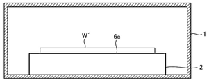
도 2a는 단계(S102)의 플라즈마 처리가 실행됨으로써, 처리 용기(1) 내의 부재의 표면에 반응 생성물(201)이 부착한 상태를 나타낸다. 도 2a에 있어서는, 처리 용기(1) 내의 부재인, 처리 용기(1)의 내벽 및 처리 용기(1) 내의 배치대(2)의 측벽의 표면에 반응 생성물(201)이 부착하고 있다. 또한, 처리 용기(1) 내의 부재에 부착한 반응 생성물(201)의 일부는, 휘발(이탈)하여 휘발성 가스(201a)로서 처리 용기(1) 내를 부유하고 있다. 도 2a의 상태인 채로, 플라즈마 처리가 실시된 기판(W)이 처리 용기(1) 내로부터 반출되면, 처리 용기(1) 내에서 배치대(2)의 배치면(6e)이 노출되고, 노출된 배치대(2)의 배치면(6e)을 향해 휘발성 가스(201a)가 끌어당겨진다. 이 때문에, 노출된 배치대(2)의 배치면(6e)에 휘발성 가스(201a)에 기초하는 반응 생성물이 부착할 가능성이 있다. 특히, 배치대(2)가 0℃ 이하의 온도까지 냉각된 상태에서 단계(S102)의 플라즈마 처리가 행해지는 경우, 휘발성 가스(201a)로서 부유하는 반응 생성물의 응축이 일어나기 쉽기 때문에, 휘발성 가스(201a)에 기초하는 반응 생성물이 배치대(2)의 배치면(6e)에 부착하기 쉬워진다. 배치대(2)의 배치면(6e)으로의 반응 생성물의 부착은, 배치대(2)의 배치면(6e)에 대한 기판(W)의 흡착 불량 등의 이상을 일으키는 요인이 되어, 바람직하지 않다.FIG. 2A shows a state in which the
따라서, 일실시 형태에서는, 단계(S102)의 플라즈마 처리의 실행 후에, 처리 용기(1) 내의 부재의 표면에, 반응 생성물(201)의 표면을 피복하는 보호막(211)을 형성한다(단계(S103), 도 2b). 즉, 처리 용기(1) 내에서 제 2 가스를 플라즈마화함으로써, 처리 용기(1) 내의 부재의 표면에 보호막(211)을 형성한다. 보호막(211)은, 반응 생성물(201)의 표면과 함께 배치대(2)의 배치면(6e) 상의 기판(W)의 표면을 피복한다. 그리고, 처리 용기(1) 내의 부재의 표면에 보호막(211)이 형성된 상태에서, 배치대(2)의 배치면(6e) 상의 기판(W)을 처리 용기(1) 내로부터 반출한다(단계(S104)).Accordingly, in one embodiment, after the plasma treatment in step S102 is performed, a
이와 같이, 단계(S102)의 플라즈마 처리의 실행 후에, 처리 용기(1) 내의 부재의 표면에, 반응 생성물(201)의 표면을 피복하는 보호막(211)을 형성함으로써, 기판(W)의 반출 시에 노출되는 배치대(2)의 배치면(6e)에 대한 반응 생성물의 부착을 저감시킬 수 있다. 예를 들면, 배치대(2)의 배치면(6e) 상의 기판(W)이 처리 용기(1) 내로부터 반출되면, 도 2c에 나타내는 바와 같이, 처리 용기(1) 내에서 배치대(2)의 배치면(6e)이 노출된다. 그러나 도 2c에 있어서는, 반응 생성물(201)의 표면을 피복하는 보호막(211)이 형성되어 있기 때문에, 반응 생성물(201)로부터 휘발(이탈)하는 휘발성 가스(201a)(도 2a 참조)가 보호막(211)에 의해 차단된다. 이에 의해, 처리 용기(1) 내에서의 휘발성 가스(201a)의 부유를 억제할 수 있고, 결과로서, 배치대(2)의 배치면(6e)에 대한 반응 생성물의 부착을 저감시킬 수 있다.In this way, after the plasma treatment in step S102 is performed, the
처리 용기(1) 내로부터 기판(W)이 반출된 후에, 처리 용기(1) 내를 클리닝한다(단계(S105), 도 2d). 클리닝에서는, 예를 들면, 처리 용기(1) 내로 더미 기판(W′)을 반입하여 배치대(2)의 배치면(6e) 상에 배치하고, 처리 용기(1) 내에서 제 3 가스를 플라즈마화함으로써, 처리 용기(1) 내의 부재의 표면에 부착한 반응 생성물(201)을 보호막(211)과 함께 제거한다. 또한, 처리 용기(1) 내로 더미 기판(W′)을 반입하지 않고, 처리 용기(1) 내에서 제 3 가스를 플라즈마화함으로써, 클리닝을 행해도 된다. 한편, 처리 용기(1) 내로부터 기판(W)이 반출된 후에, 기판(W)의 표면을 피복하는 보호막(211)을 제거한다(단계(S106)). 이 때, 기판(W) 상의 마스크로서, 레지스트 또는 아몰퍼스 카본 등의 탄소 함유 마스크가 이용되고 있는 경우, 기판(W)의 표면을 피복하는 보호막(211)과 함께 기판(W) 상의 마스크도 제거한다.After the substrate W is taken out from the inside of the
[보호막의 형성에 이용하는 제 2 가스의 선정][Selection of a second gas to be used for forming a protective film]
보호막의 형성에 이용하는 제 2 가스는, 단계(S102)의 기판에 대한 플라즈마 처리를 실행함으로써 노출된 기판 상의 막의 표면(상면, 측면)에 대하여 에천트로서 기능하지 않는 가스인 것이 바람직하다. 따라서, 본 발명자들은, 각종의 가스에 관하여, 기판 상의 노출된 막의 표면에 대한 에천트로서의 기능의 유무에 대하여 조사했다. 실험에서는, 실리콘 기판 상에 적층된 실리콘 산화막(이하 'SiO2막'이라 칭함)을 기판 상의 노출된 막으로서 가지는 기판을 CF4, CH4 및 C4F8 각각의 플라즈마에 노출시켰다. SiO2막에는, 패턴이 형성되어 있다. 도 3은 가스종마다, 플라즈마에 노출된 기판 상의 에칭 대상막의 상태를 비교한 결과의 일례를 나타내는 도이다. 도 3에 있어서, 'Initial'은, 단계(S102)의 플라즈마 처리를 실행함으로써 SiO2막 상에 형성된 개구부를 가지는 마스크를 통하여, SiO2막에 홀 형상의 패턴을 에칭 가공한 후의 기판을 나타낸다. 또한, 실험의 효과를 알기 쉽게 하기 위하여, 에칭 가공 후, 마스크를 제거한 것을 이용하고 있으며, SiO2막의 상면과 측면이 노출되어 있다.The second gas used for forming the protective film is preferably a gas that does not function as an etchant with respect to the surface (top surface, side surface) of the film on the substrate exposed by performing plasma processing on the substrate in step S102. Therefore, the present inventors investigated the presence or absence of a function as an etchant for the surface of the exposed film on the substrate with respect to various gases. In the experiment, a substrate having a silicon oxide film (hereinafter referred to as 'SiO 2 film') laminated on a silicon substrate as an exposed film on the substrate was exposed to plasma of each of CF 4 , CH 4 and C 4 F 8 . A pattern is formed in the SiO 2 film. 3 is a diagram showing an example of a result of comparing the state of the etching target film on the substrate exposed to plasma for each gas type. In FIG. 3 , 'Initial' denotes a substrate after etching a hole-shaped pattern on the SiO 2 film through a mask having an opening formed on the SiO 2 film by performing the plasma processing of step S102. In addition, in order to make it easy to understand the effect of the experiment, the mask removed after etching is used, and the top and side surfaces of the SiO 2 film are exposed.
도 3에 나타내는 바와 같이, CF4 또는 C4F8를 이용하는 경우, 기판 상의 노출된 막인 SiO2막이 깎여, 그 막 두께가 감소하고 있다. 이에 대하여, CH4를 이용하는 경우, 기판 상의 SiO2막의 상면 및 SiO2막의 패턴 저부에 퇴적물이 퇴적되어 있다. 이와 같이, 도 3의 결과로부터, 할로겐을 포함하지 않는 탄소 함유 가스를 이용함으로써, 기판 상의 노출된 막의 패턴 형상을 유지할 수 있는 것을 알 수 있다. 즉, 보호막의 형성에 이용하는 제 2 가스는, 할로겐을 포함하지 않는 탄소 함유 가스인 것이 바람직하며, 탄화수소 가스인 것이 보다 바람직하다.As shown in FIG. 3 , when CF 4 or C 4 F 8 is used, the SiO 2 film that is an exposed film on the substrate is scraped, and the film thickness thereof is decreasing. In contrast, when CH 4 is used, deposits are deposited on the upper surface of the SiO 2 film on the substrate and on the bottom of the pattern of the SiO 2 film. As described above, from the results of FIG. 3 , it is understood that the pattern shape of the exposed film on the substrate can be maintained by using the halogen-free carbon-containing gas. That is, it is preferable that it is a carbon containing gas which does not contain a halogen, and, as for the 2nd gas used for formation of a protective film, it is more preferable that it is a hydrocarbon gas.
또한 상기 실시 형태에서는, 단계(S102)의 기판에 대한 플라즈마 처리를 에칭 처리라 하고, 에칭 대상막 및 에칭 처리 후에 노출된 기판 상의 막을 SiO2막이라 했지만, 개시 기술은 임의의 에칭 대상막에 채용될 수 있다. 예를 들면, 에칭 대상막은, 실리콘 질화막(SiN막), 실리콘 탄화막(SiC막) 등의 단층막, 또는 실리콘 산화막과 실리콘 질화막이 교호로 적층된 적층막(ON 적층막)이어도 된다. 또한, 단결정 실리콘(Si), 다결정 실리콘(Poly-Si), 아몰퍼스 실리콘(αSi) 등의 실리콘막이어도 되고, 실리콘 산화막과 다결정 실리콘이 교호로 적층된 적층막(OP적층막)이어도 된다. 또한, SiOCH 구조를 가지는 저유전율막이어도 된다. 이들을 총괄하여, '실리콘 함유막'이라 칭한다. 또한, 에칭 대상막이 에칭되어, 하지막까지 도달했을 때, 하지막이 노출된다. 하지막으로서는, 티탄(Ti) 또는 텅스텐(W), 구리(Cu) 등의 금속막 또는 실리콘막이 이용된다. 에칭의 마스크로서, 질화 티탄(TiN) 또는 텅스텐(W) 등의 금속막 또는 실리콘막이 이용되고 있고, 에칭 처리 후, 기판 상에서 노출된 상태가 된다.Further, in the above embodiment, the plasma treatment on the substrate in step S102 is referred to as an etching treatment, and the film to be etched and the film on the substrate exposed after the etching treatment is referred to as a SiO 2 film. can be For example, the etching target film may be a single-layer film such as a silicon nitride film (SiN film) or a silicon carbide film (SiC film), or a laminate film (ON lamination film) in which a silicon oxide film and a silicon nitride film are alternately stacked. Further, a silicon film such as single crystal silicon (Si), polycrystalline silicon (Poly-Si), or amorphous silicon (αSi) may be used, or a laminate film (OP laminate film) in which a silicon oxide film and polycrystalline silicon are alternately laminated may be used. Moreover, the low-dielectric-constant film|membrane which has a SiOCH structure may be sufficient. These are collectively referred to as a 'silicon-containing film'. Further, when the etching target film is etched to reach the underlying film, the underlying film is exposed. As the base film, a metal film such as titanium (Ti), tungsten (W), copper (Cu), or a silicon film is used. As a mask for etching, a metal film or silicon film such as titanium nitride (TiN) or tungsten (W) is used, and is exposed on the substrate after the etching process.
이들 실리콘 함유막 및 금속막에 대하여, SiO2막과 마찬가지로, 보호막의 형성에 이용하는 제 2 가스는, 에천트로서 기능하지 않는 가스인 것이 바람직하다. 또한, 실리콘 함유막 및 금속막은 할로겐이 포함되는 환경 하에서는 깎이기 쉬운 것은 알려져 있기 때문에, 기판 상의 노출된 막이 실리콘 함유막 및 금속막인 경우도, SiO2막인 경우와 마찬가지로, 보호막의 형성에 이용하는 제 2 가스는, 할로겐을 포함하지 않는 탄소 함유 가스인 것이 바람직하며, 탄화수소 가스인 것이 보다 바람직하다.For these silicon-containing films and metal films, like the SiO 2 film, the second gas used to form the protective film is preferably a gas that does not function as an etchant. In addition, since it is known that the silicon-containing film and the metal film are easy to be scraped under an environment containing a halogen, when the exposed films on the substrate are the silicon-containing film and the metal film, as in the case of the SiO 2 film, the agent used for forming the protective film It is preferable that it is a carbon-containing gas which does not contain a halogen, and, as for 2 gas, it is more preferable that it is a hydrocarbon gas.
[보호막의 제거][Removal of the protective film]
상기와 같이, 기판의 표면을 피복하는 보호막은, 처리 용기 내로부터 기판이 반출된 후에 제거된다(단계(S106)). 또한, 기판 상의 마스크로서 탄소 함유 마스크를 이용한 경우, 기판의 표면을 피복하는 보호막과 동시에 기판 상의 마스크도 제거된다. 본 발명자들은, 일실시 형태에 따른 플라즈마 처리 방법으로 기판을 에칭 처리하고, 마스크의 제거 후의 에칭 대상막의 패턴 형상, 즉, 기판 상의 노출된 막의 패턴 형상을 조사했다. 도 4는 비교예 1에 따른 처리 후의 기판 상의 에칭 대상막의 상태와, 실험예 1에 따른 처리 후의 기판 상의 에칭 대상막의 상태를 비교한 결과의 일례를 나타내는 도이다. 도 4에 있어서, 'Etch → Depo → Ash'는, 실험예 1의 결과이며, 일실시 형태에 따른 플라즈마 처리 방법으로 기판을 에칭 처리하고, 마스크를 제거한 경우이다. 또한, 'Etch → Ash'는, 비교예 1의 결과이며, 보호막을 형성하지 않고 기판을 에칭 처리하고, 마스크를 제거한 경우이다. 또한, 실험에서는, 실리콘 기판 상에 SiO2막을 에칭 대상막으로서 가지는 기판이 이용되었다. 또한, 기판 상의 마스크는, 탄소 함유 마스크이며, 단계(S106)에 있어서 산소의 플라즈마를 이용하여 제거되었다.As described above, the protective film covering the surface of the substrate is removed after the substrate is taken out from the processing container (step S106). In addition, when a carbon-containing mask is used as the mask on the substrate, the mask on the substrate is removed simultaneously with the protective film covering the surface of the substrate. The present inventors etched the substrate by the plasma processing method according to the embodiment, and investigated the pattern shape of the etching target film after removal of the mask, that is, the pattern shape of the exposed film on the substrate. 4 is a diagram showing an example of a result of comparing the state of the etching target film on the substrate after the treatment according to Comparative Example 1 and the etching target film on the substrate after the treatment according to Experimental Example 1. FIG. In FIG. 4 , 'Etch → Depo → Ash' is a result of Experimental Example 1, in which the substrate is etched by the plasma processing method according to the embodiment and the mask is removed. In addition, 'Etch → Ash' is the result of the comparative example 1, It is a case where the board|substrate was etched without forming a protective film, and the mask was removed. In addition, in the experiment, a substrate having a SiO 2 film as an etching target film on a silicon substrate was used. In addition, the mask on the substrate is a carbon-containing mask and is removed by using plasma of oxygen in step S106.
도 4에 나타내는 바와 같이, 실험예 1에 의한 처리 후의 에칭 대상막의 패턴 형상, 즉, 기판 상의 노출된 막의 패턴 형상은, 비교예 1에 의한 처리 후의 에칭 대상막의 패턴 형상과 거의 동등했다. 이와 같이, 도 4의 결과로부터, 기판의 표면을 피복하는 보호막은, 기판 상의 마스크(즉, 탄소 함유 마스크)와 동시에 적절하게 제거되는 것이 확인되었다.As shown in FIG. 4 , the pattern shape of the etching target film after the treatment according to Experimental Example 1, that is, the pattern shape of the exposed film on the substrate, was substantially the same as the pattern shape of the etching target film after the treatment according to Comparative Example 1. As described above, it was confirmed from the results of FIG. 4 that the protective film covering the surface of the substrate was appropriately removed simultaneously with the mask on the substrate (that is, the carbon-containing mask).
[보호막의 최소 막 두께][Minimum film thickness of the protective film]
처리 용기 내의 부재의 표면에 보호막이 형성되었다 하더라도, 보호막이 얇은 경우에는, 반응 생성물로부터 이탈하는 휘발성 가스가 보호막을 투과하여 처리 용기 내를 부유하기 때문에, 휘발성 가스에 기초하는 반응 생성물이 노출된 배치대의 배치면에 부착할 가능성이 있다. 따라서, 보호막의 두께와 처리 용기 내의 클리닝 시의 트러블의 유무와의 관계에 대하여 조사했다.Even if a protective film is formed on the surface of a member in the processing container, when the protective film is thin, the volatile gas leaving the reaction product passes through the protective film and floats in the processing container, so that the reaction product based on the volatile gas is exposed. There is a possibility of attaching to the arrangement surface of the stand. Therefore, the relationship between the thickness of a protective film and the presence or absence of the trouble at the time of cleaning in a processing container was investigated.
도 5는 보호막의 두께와 처리 용기 내의 클리닝 시의 트러블의 유무와의 관계를 조사한 실험 결과의 일례를 나타내는 도이다. 도 5에 나타내는 실험에서는, 단계(S103)에서 형성되는 보호막의 두께를 5 종류로 설정하고, 단계(S105)의 클리닝의 실행 중에, 배치대의 배치면과 더미 기판과의 사이로 공급되는 전열 가스(He 가스)의 리크량을 측정함으로써, 트러블의 유무를 조사했다. 보호막의 두께를 0(nm), 25(nm), 50(nm), 100(nm), 150(nm)의 5 종류로 설정했다. 또한, 단계(S104)의 배치대의 배치면 상의 기판을 처리 용기 내로부터 반출하여, 단계(S105)의 처리 용기 내로 더미 기판을 반입하여 배치대의 배치면 상에 배치할 때까지의 동안, 600초의 간격을 두고 있다. 이는, 통상의 기판의 반출, 및 더미 기판의 반입에 걸리는 시간보다 충분히 길다. 그리고, 배치대의 배치면과 더미 기판과의 사이로 공급되는 전열 가스의 리크량이 미리 정해진 허용 스펙을 초과하는 경우, 트러블의 발생이 있다고 판단되었다. 한편, 전열 가스의 리크량이 허용 스펙 이하인 경우, 트러블의 발생이 없다고 판단되었다. 또한, 배치대의 배치면에 반응 생성물이 부착함으로써, 배치대의 배치면에 대한 더미 기판의 흡착력이 저하되고, 결과로서, 전열 가스의 리크량이 증대하는 것이라고 상정된다.5 is a diagram showing an example of the experimental result of examining the relationship between the thickness of the protective film and the presence or absence of a trouble at the time of cleaning in the processing container. In the experiment shown in Fig. 5, the thickness of the protective film formed in step S103 is set to five, and the heat transfer gas (He) supplied between the mounting surface of the mounting table and the dummy substrate during the cleaning in step S105 is performed The presence or absence of a trouble was investigated by measuring the leak amount of gas). The thickness of the protective film was set to 5 types of 0 (nm), 25 (nm), 50 (nm), 100 (nm), and 150 (nm). In addition, an interval of 600 seconds between unloading the substrate on the mounting surface of the mounting table in step S104 from the inside of the processing container and loading the dummy substrate into the processing vessel in step S105 to placing it on the mounting surface of the mounting table is putting This is sufficiently longer than the time taken for carrying out the normal substrate and carrying in the dummy substrate. And, when the leakage amount of the heat transfer gas supplied between the mounting surface of the mounting table and the dummy substrate exceeds a predetermined allowable specification, it was determined that a trouble occurred. On the other hand, when the leak amount of the heat transfer gas was below an allowable specification, it was judged that there was no generation|occurrence|production of a trouble. Further, it is assumed that the adhesion of the reaction product to the mounting surface of the mounting table lowers the adsorption force of the dummy substrate with respect to the mounting surface of the mounting table, and as a result, the amount of leakage of the heat transfer gas increases.
도 5에 나타내는 바와 같이, 보호막의 두께가 100(nm) 이상인 경우, 처리 용기 내의 클리닝 시의 트러블의 발생이 없었다. 즉, 도 5의 결과로부터, 보호막이 100(nm) 이상의 두께인 경우, 휘발성 가스가 보호막을 투과하기 어려워져, 휘발성 가스에 기초하는 반응 생성물이 배치대의 배치면에 부착하는 것이 억제되는 것이 확인되었다. 따라서, 보호막은, 100 nm 이상의 두께로 형성되는 것이 바람직하다.As shown in FIG. 5 , when the thickness of the protective film was 100 (nm) or more, there was no occurrence of trouble during cleaning in the processing container. That is, from the results of FIG. 5 , it was confirmed that, when the protective film had a thickness of 100 (nm) or more, it was difficult for volatile gases to permeate through the protective film, and it was confirmed that the adhesion of reaction products based on volatile gases to the mounting surface of the mounting table was suppressed. . Therefore, it is preferable that the protective film be formed to a thickness of 100 nm or more.
[일실시 형태에 따른 플라즈마 처리 장치의 일례][Example of plasma processing apparatus according to an embodiment]
도 6은 일실시 형태에 따른 플라즈마 처리 방법의 실행에 이용되는 플라즈마 처리 장치(10)의 일례를 나타내는 도이다. 플라즈마 처리 장치(10)는, 기밀하게 구성되고, 전기적으로 접지 전위가 된 처리 용기(1)를 가지고 있다. 이 처리 용기(1)는, 원통 형상이 되고, 예를 들면 알루미늄 등으로 구성되어 있다. 처리 용기(1)는, 플라즈마가 생성되는 처리 공간을 구획 형성한다. 처리 용기(1) 내에는, 반도체 웨이퍼 등의 기판(W)을 수평으로 지지하는 배치대(2)가 마련되어 있다. 배치대(2)는, 기재(베이스)(2a) 및 정전 척(ESC : Electrostatic chuck)(6)을 포함하여 구성되어 있다. 기재(2a)는, 도전성의 금속, 예를 들면 알루미늄 등으로 구성되어 있고, 하부 전극으로서의 기능을 가진다. 정전 척(6)은, 기판(W)을 정전 흡착하기 위한 기능을 가진다. 배치대(2)는, 지지대(4)에 지지되어 있다. 지지대(4)는, 예를 들면 석영 등으로 이루어지는 지지 부재(3)에 지지되어 있다. 또한, 배치대(2)의 상방의 외주에는, 예를 들면 단결정 실리콘으로 형성된 포커스 링(5)이 마련되어 있다. 또한, 처리 용기(1) 내에는, 배치대(2) 및 지지대(4)의 주위를 둘러싸도록, 예를 들면 석영 등으로 이루어지는 원통 형상의 내벽 부재(3a)가 마련되어 있다.6 is a diagram illustrating an example of the
기재(2a)에는, 제 1 정합기(11a)를 개재하여 제 1 RF 전원(10a)이 접속되고, 또한, 제 2 정합기(11b)를 개재하여 제 2 RF 전원(10b)이 접속되어 있다. 제 1 RF 전원(10a)은, 플라즈마 발생용의 것이며, 이 제 1 RF 전원(10a)으로부터는 정해진 주파수의 고주파 전력이 배치대(2)의 기재(2a)에 공급되도록 구성되어 있다. 또한, 제 2 RF 전원(10b)은, 이온 인입용(바이어스용)의 것이며, 이 제 2 RF 전원(10b)으로부터는 제 1 RF 전원(10a)보다 낮은 정해진 주파수의 고주파 전력이 배치대(2)의 기재(2a)에 공급되도록 구성되어 있다. 이와 같이, 배치대(2)는 전압 인가 가능하게 구성되어 있다. 한편, 배치대(2)의 상방에는, 배치대(2)와 평행하게 대향하도록, 상부 전극으로서의 기능을 가지는 샤워 헤드(16)가 마련되어 있다. 샤워 헤드(16)와 배치대(2)는, 한 쌍의 전극(상부 전극과 하부 전극)으로서 기능한다.A first
정전 척(6)은, 상면이 평탄한 원반 형상으로 형성되고, 당해 상면이 기판(W)이 배치되는 배치면(6e)으로 되어 있다. 정전 척(6)은, 해당 절연체(6b)의 사이에 전극(6a)을 개재시켜 구성되어 있고, 전극(6a)에는 직류 전원(12)이 접속되어 있다. 그리고 전극(6a)에 직류 전원(12)으로부터 직류 전압이 인가됨으로써, 쿨롱력에 의해 기판(W)이 흡착되도록 구성되어 있다.The
배치대(2)의 내부에는, 냉매 유로(2d)가 형성되어 있고, 냉매 유로(2d)에는, 냉매 입구 배관(2b), 냉매 출구 배관(2c)이 접속되어 있다. 그리고, 냉매 유로(2d) 내에 적절한 냉매, 예를 들면 냉각수 등을 순환시킴으로써, 배치대(2)를 정해진 온도로 제어 가능하게 구성되어 있다. 또한, 배치대(2) 등을 관통하도록, 기판(W)의 이면으로 헬륨 가스 등의 냉열 전달용 가스(백 사이드 가스)를 공급하기 위한 가스 공급관(30)이 마련되어 있고, 가스 공급관(30)은, 도시하지 않는 가스 공급원에 접속되어 있다. 이들 구성에 의해, 배치대(2)의 상면에 정전 척(6)에 의해 흡착 유지된 기판(W)을, 정해진 온도로 제어한다.A
배치대(2)에는, 복수, 예를 들면 3 개의 핀용 관통홀(200)이 마련되어 있고(도 6에는 1 개만 나타냄), 이들 핀용 관통홀(200)의 내부에는, 각각 리프터 핀(61)이 배치되어 있다. 리프터 핀(61)은, 승강 기구(62)에 접속되어 있다. 승강 기구(62)는, 리프터 핀(61)을 승강시켜, 배치대(2)의 배치면(6e)에 대하여 리프터 핀(61)을 출몰 가능하게 동작시킨다. 리프터 핀(61)을 상승시킨 상태에서는, 리프터 핀(61)의 선단이 배치대(2)의 배치면(6e)으로부터 돌출하여, 배치대(2)의 배치면(6e)의 상방에 기판(W)을 유지한 상태가 된다. 한편, 리프터 핀(61)을 하강시킨 상태에서는, 리프터 핀(61)의 선단이 핀용 관통홀(200) 내에 수용되고, 기판(W)이 배치대(2)의 배치면(6e)에 배치된다. 이와 같이, 승강 기구(62)는, 리프터 핀(61)에 의해 배치대(2)의 배치면(6e)에 대하여 기판(W)을 승강시킨다. 또한, 승강 기구(62)는, 리프터 핀(61)을 상승시킨 상태에서는, 리프터 핀(61)에 의해 배치대(2)의 배치면(6e)의 상방에 기판(W)을 유지한다.The mounting table 2 is provided with a plurality of, for example, three through-
상기한 샤워 헤드(16)는, 처리 용기(1)의 천벽 부분에 마련되어 있다. 샤워 헤드(16)는, 본체부(16a)와 전극판을 이루는 상부 천판(16b)을 구비하고 있고, 절연성 부재(95)를 개재하여 처리 용기(1)의 상부에 지지된다. 본체부(16a)는, 도전성 재료, 예를 들면 표면이 양극 산화 처리된 알루미늄으로 이루어지고, 그 하부에 상부 천판(16b)을 착탈 가능하게 지지할 수 있도록 구성되어 있다.The above-described
본체부(16a)는, 내부에 가스 확산실(16c)이 마련되어 있다. 또한, 본체부(16a)는, 가스 확산실(16c)의 하부에 위치하도록, 저부에, 다수의 가스 통류홀(16d)이 형성되어 있다. 또한, 상부 천판(16b)은, 당해 상부 천판(16b)을 두께 방향으로 관통하도록 가스 도입홀(16e)이, 상기한 가스 통류홀(16d)과 중첩되도록 마련되어 있다. 이러한 구성에 의해, 가스 확산실(16c)로 공급된 처리 가스는, 가스 통류홀(16d) 및 가스 도입홀(16e)을 거쳐 처리 용기(1) 내에 샤워 형상으로 분산되어 공급된다.The
본체부(16a)에는, 가스 확산실(16c)로 처리 가스를 도입하기 위한 가스 도입구(16g)가 형성되어 있다. 가스 도입구(16g)에는, 가스 공급 배관(15a)의 일단이 접속되어 있다. 이 가스 공급 배관(15a)의 타단에는, 처리 가스를 공급하는 처리 가스 공급원(가스 공급부)(15)이 접속된다. 가스 공급 배관(15a)에는, 상류측으로부터 차례로 매스 플로우 컨트롤러(MFC)(15b), 및 개폐 밸브(V2)가 마련되어 있다. 가스 확산실(16c)에는, 가스 공급 배관(15a)을 거쳐, 처리 가스 공급원(15)으로부터 각종 처리 가스가 공급된다. 처리 가스 공급원(15)은, 복수의 가스 소스를 가지고 있다. 복수의 가스 소스는, 탄화수소 가스의 가스 소스, 산소 원자를 가지는 가스(산소 가스 등)의 소스, 및 불활성 가스의 소스 등의 각종의 가스의 소스를 포함할 수 있다. 불활성 가스로서는, 질소 가스, Ar 가스, He 가스와 같은 임의의 가스가 이용될 수 있다. 따라서, 플라즈마 처리 장치(10)는, 처리 가스 공급원(15)의 복수의 가스 소스 중 선택된 하나 이상의 가스 소스로부터의 가스를, 개별로 조정된 유량으로, 처리 용기(1) 내에 공급하는 것이 가능하다.A
상기한 상부 전극으로서의 샤워 헤드(16)에는, 로우패스 필터(LPF)(71)를 개재하여 가변 직류 전원(72)이 전기적으로 접속되어 있다. 이 가변 직류 전원(72)은, 온·오프 스위치(73)에 의해 급전의 온·오프가 가능하게 구성되어 있다. 가변 직류 전원(72)의 전류·전압 그리고 온·오프 스위치(73)의 온·오프는, 후술하는 제어부(100)에 의해 제어된다. 또한, 후술하는 바와 같이, 제 1 RF 전원(10a), 제 2 RF 전원(10b)으로부터 고주파가 배치대(2)에 인가되어 처리 공간에 플라즈마가 발생할 시에는, 필요에 따라 제어부(100)에 의해 온·오프 스위치(73)가 온이 되어, 상부 전극으로서의 샤워 헤드(16)에 정해진 직류 전압이 인가된다.A variable
처리 용기(1)의 측벽으로부터 샤워 헤드(16)의 높이 위치보다 상방으로 연장되도록 원통 형상의 접지 도체(1a)가 마련되어 있다. 이 원통 형상의 접지 도체(1a)는, 그 상부에 천벽을 가지고 있다.A
처리 용기(1)의 저부에는, 배기구(81)가 형성되어 있다. 배기구(81)에는, 배기관(82)을 개재하여 배기 장치(83)가 접속되어 있다. 배기 장치(83)는, 진공 펌프를 가지고 있고, 이 진공 펌프를 작동시킴으로써 처리 용기(1) 내를 정해진 진공도까지 감압할 수 있도록 구성되어 있다. 한편, 처리 용기(1) 내의 측벽에는, 기판(W)의 반입반출구(84)가 마련되어 있고, 이 반입반출구(84)에는, 당해 반입반출구(84)를 개폐하는 게이트 밸브(85)가 마련되어 있다.An
처리 용기(1)의 측부 내측에는, 내벽면을 따라 퇴적물 실드(86)가 마련되어 있다. 퇴적물 실드(86)는, 처리 용기(1)에 에칭 부생성물(퇴적물)이 부착하는 것을 방지한다. 이 퇴적물 실드(86)의 기판(W)과 대략 동일한 높이 위치에는, 그라운드에 대한 전위가 제어 가능하게 접속된 도전성 부재(GND 블록)(89)가 마련되어 있고, 이에 의해 이상 방전이 방지된다. 또한, 퇴적물 실드(86)의 하단부에는, 내벽 부재(3a)를 따라 연장되는 퇴적물 실드(87)가 마련되어 있다. 퇴적물 실드(86, 87)는 착탈 가능하게 되어 있다.On the inner side of the side of the
또한, 플라즈마 처리 장치(10)는, 예를 들면 도 6에 나타내는 바와 같이, 프로세서 및 메모리 등을 포함하는 제어부(100)를 구비한다. 제어부(100)는, 플라즈마 처리 장치(10)의 각 부를 제어한다. 제어부(100)는, 구체적으로, 제어 신호를 이용하여, 처리 가스 공급원(15)으로부터의 가스의 선택 및 유량, 배기 장치(83)의 배기, 제 1 RF 전원(10a) 및 제 2 RF 전원(10b)으로부터의 전력 공급, 가변 직류 전원(72)으로부터의 전압 인가, 리프터 핀(61)의 승강 등을 제어한다. 또한, 본 명세서에 있어서 개시되는 플라즈마 처리 방법의 각 공정은, 제어부(100)에 의한 제어에 의해 플라즈마 처리 장치(10)의 각 부를 동작시킴으로써 실행될 수 있다. 제어부(100)의 메모리에는, 일실시 형태에 따른 플라즈마 처리 방법을 실행하기 위한 컴퓨터 프로그램, 및, 당해 방법의 실행에 이용되는 각종의 데이터가, 읽어내기 가능하게 저장되어 있다.Further, the
[실시 형태의 효과][Effect of embodiment]
실시 형태에 따른 플라즈마 처리 방법은, 처리 용기 내로 기판을 반입하여 처리 용기 내의 배치대의 배치면 상에 배치하는 공정과, 처리 용기 내에서 제 1 가스를 플라즈마화함으로써, 기판에 대한 플라즈마 처리를 실행하는 공정과, 처리 용기 내에서 제 2 가스를 플라즈마화함으로써, 플라즈마 처리의 실행 시에 처리 용기 내의 부재의 표면에 부착한 반응 생성물의 표면을 피복하는 막을 형성하는 공정과, 처리 용기 내의 부재의 표면에 막이 형성된 상태에서, 배치대의 배치면 상의 기판을 처리 용기 내로부터 반출하는 공정을 포함한다. 이에 의해, 배치대의 배치면에 대한 반응 생성물의 부착을 저감시킬 수 있다.A plasma processing method according to an embodiment includes a step of loading a substrate into a processing container and arranging it on a mounting surface of a mounting table in the processing container, and plasma processing of a substrate by converting a first gas into plasma in the processing container. A process comprising: forming a film covering the surface of a reaction product adhering to a surface of a member in the processing container when plasma processing is performed by plasmaizing the second gas in the processing container; and discharging the substrate on the mounting surface of the mounting table from the inside of the processing vessel in a state in which the film is formed. Thereby, adhesion of the reaction product to the mounting surface of the mounting table can be reduced.
또한, 실시 형태에 있어서, 반출하는 공정 후에, 처리 용기 내에서 제 3 가스를 플라즈마화함으로써, 반응 생성물을 막과 함께 제거하는 공정을 더 포함해도 된다. 이에 의해, 반응 생성물의 표면을 피복하는 보호막을 반응 생성물과 동시에 제거할 수 있다.Moreover, in an embodiment, after the process of carrying out, you may further include the process of removing a reaction product together with a film|membrane by converting a 3rd gas into plasma in a processing container. Thereby, the protective film covering the surface of the reaction product can be removed simultaneously with the reaction product.
또한, 실시 형태에 있어서의 막을 형성하는 공정에 있어서, 기판의 표면이 반응 생성물의 표면과 함께 막으로 피복되어도 된다. 또한, 실시 형태에 있어서, 반출하는 공정 후에, 반출된 기판의 표면을 피복하는 막과 함께 기판 상의 마스크를 제거하는 공정을 더 포함해도 된다. 이에 의해, 기판의 표면을 피복하는 보호막을 기판 상의 마스크와 함께 적절히 제거할 수 있고, 결과로서, 마스크 아래의 패턴 형상을 유지 가능하다.Further, in the step of forming the film in the embodiment, the surface of the substrate may be coated with the film together with the surface of the reaction product. Moreover, in embodiment, after the process of carrying out, you may further include the process of removing the mask on a board|substrate together with the film|membrane which coat|covers the surface of the board|substrate carried out. Thereby, the protective film covering the surface of the substrate can be appropriately removed together with the mask on the substrate, and as a result, the pattern shape under the mask can be maintained.
또한, 실시 형태에 있어서, 제 2 가스는, 기판 상의 노출된 막에 대하여 에천트로서 기능하지 않는 가스여도 된다. 이에 의해, 보호막의 형성 시에 기판 상의 노출된 막의 패턴 형상을 유지 가능하다.In the embodiment, the second gas may be a gas that does not function as an etchant for an exposed film on the substrate. Thereby, the pattern shape of the film|membrane exposed on a board|substrate at the time of formation of a protective film can be maintained.
또한, 실시 형태에 있어서, 기판 상의 노출된 막은, 실리콘 산화막(SiO2막)이며, 제 2 가스는, 할로겐을 포함하지 않는 탄소 함유 가스여도 된다. 또한, 실시 형태에 있어서, 제 2 가스는, 탄화수소 가스여도 된다. 이에 의해, 보호막의 형성 시에 기판 상의 노출된 막인 SiO2막의 패턴 형상을 유지 가능하다.In the embodiment, the exposed film on the substrate is a silicon oxide film (SiO 2 film), and the second gas may be a halogen-free carbon-containing gas. In addition, in embodiment, hydrocarbon gas may be sufficient as 2nd gas. As a result, it is possible to keep the SiO 2 film, a film-like pattern exposed on the substrate in the formation of the protective film.
또한, 실시 형태에 있어서의 막을 형성하는 공정에 있어서, 막은, 100 nm 이상의 두께로 처리 용기 내의 부재의 표면에 형성되어도 된다. 이에 의해, 반응 생성물로부터 이탈하는 휘발성 가스가 보호막을 투과하기 어려워지고, 결과로서, 휘발성 가스에 기초하는 반응 생성물이 배치대의 배치면에 부착하는 것을 억제할 수 있다.Further, in the step of forming the film in the embodiment, the film may be formed on the surface of the member in the processing container to a thickness of 100 nm or more. This makes it difficult for the volatile gas to escape from the reaction product to permeate the protective film, and as a result, it is possible to suppress adhering of the reaction product based on the volatile gas to the mounting surface of the mounting table.
또한, 실시 형태에 있어서, 처리 용기 내의 부재의 표면 온도는, 플라즈마 처리의 실행 시의 배치대의 온도 이하이며, 막으로부터 이탈하는 가스는, 처리 용기 내의 부재의 표면에 부착하지 않는 성질을 가져도 된다. 이에 의해, 처리 용기 내의 부재의 표면 온도가 낮은 경우라도, 막으로부터 이탈하는 가스가 처리 용기 내의 부재의 표면에 부착하는 것을 억제할 수 있다.Further, in an embodiment, the surface temperature of the member in the processing container is equal to or less than the temperature of the mounting table when plasma processing is performed, and the gas leaving the film may have a property that does not adhere to the surface of the member in the processing container. . Accordingly, even when the surface temperature of the member in the processing container is low, it is possible to suppress the gas leaving the film from adhering to the surface of the member in the processing container.
또한, 금회 개시된 실시 형태는 모든 점에서 예시로 제한적인 것은 아니라고 생각되어야 한다. 상기의 실시 형태는, 첨부한 청구의 범위 및 그 주지를 일탈하지 않고, 다양한 형태로 생략, 치환, 변경되어도 된다.In addition, it should be thought that embodiment disclosed this time is not restrictive by an illustration in all points. Said embodiment may be abbreviate|omitted, substituted, and may be changed in various forms, without deviating from the attached claim and the main point.
예를 들면, 상기의 실시 형태에서는, 플라즈마 처리 장치(10)는, 용량 결합형의 플라즈마 처리 장치(10)였지만, 임의의 플라즈마 처리 장치(10)에 채용될 수 있다. 예를 들면, 플라즈마 처리 장치(10)는, 유도 결합형의 플라즈마 처리 장치(10), 마이크로파와 같은 표면파에 의해 가스를 여기시키는 플라즈마 처리 장치(10)와 같이, 임의의 타입의 플라즈마 처리 장치(10)여도 된다.For example, in the above embodiment, the
Claims (9)
상기 처리 용기 내에서 제 1 가스를 플라즈마화함으로써, 상기 기판에 대한 플라즈마 처리를 실행하는 공정과,
상기 처리 용기 내에서 제 2 가스를 플라즈마화함으로써, 상기 플라즈마 처리의 실행 시에 상기 처리 용기 내의 부재의 표면에 부착한 반응 생성물의 표면을 피복하는 막을 형성하는 공정과,
상기 처리 용기 내의 부재의 표면에 상기 막이 형성된 상태에서, 상기 배치대의 배치면 상의 기판을 상기 처리 용기 내로부터 반출하는 공정
을 포함하는, 플라즈마 처리 방법.a step of loading a substrate into a processing container and arranging it on a mounting surface of a mounting table in the processing container;
performing plasma processing on the substrate by converting a first gas into plasma in the processing chamber;
forming a film covering the surface of a reaction product adhering to a surface of a member in the processing chamber during execution of the plasma processing by plasmaizing the second gas in the processing chamber;
a step of unloading the substrate on the mounting surface of the mounting table from the inside of the processing vessel while the film is formed on the surface of the member in the processing vessel
A plasma treatment method comprising a.
상기 반출하는 공정 후에, 상기 처리 용기 내에서 제 3 가스를 플라즈마화함으로써, 상기 반응 생성물을 상기 막과 함께 제거하는 공정을 더 포함하는, 플라즈마 처리 방법.The method of claim 1,
The plasma processing method further comprising a step of removing the reaction product together with the film by plasmaizing the third gas in the processing container after the step of carrying out the carrying out process.
상기 막을 형성하는 공정에 있어서,
상기 기판의 표면이 상기 반응 생성물의 표면과 함께 상기 막으로 피복되고,
상기 반출하는 공정 후에, 반출된 상기 기판의 표면을 피복하는 상기 막을 제거하는 공정을 더 포함하는, 플라즈마 처리 방법.3. The method of claim 1 or 2,
In the process of forming the film,
the surface of the substrate is covered with the film together with the surface of the reaction product;
The plasma processing method further comprising the process of removing the said film|membrane which coat|covers the surface of the said board|substrate which was carried out after the said carrying out process.
상기 제 2 가스는, 플라즈마 처리를 실행하는 공정에 의해 상기 기판 상에서 노출되는 막의 표면에 대하여 에천트로서 기능하지 않는 가스인, 플라즈마 처리 방법.4. The method according to any one of claims 1 to 3,
The second gas is a gas that does not function as an etchant with respect to a surface of a film exposed on the substrate by the step of performing plasma processing.
상기 기판 상에서 노출되는 막은, 실리콘 함유막 또는 금속막이며,
상기 제 2 가스는, 할로겐을 포함하지 않는 탄소 함유 가스인, 플라즈마 처리 방법.5. The method of claim 4,
The film exposed on the substrate is a silicon-containing film or a metal film,
The second gas is a carbon-containing gas that does not contain a halogen.
상기 제 2 가스는, 탄화수소 가스인, 플라즈마 처리 방법.6. The method of claim 5,
The second gas is a hydrocarbon gas.
상기 막을 형성하는 공정에 있어서,
상기 막은, 100 nm 이상의 두께로 상기 처리 용기 내의 부재의 표면에 형성되는, 플라즈마 처리 방법.7. The method according to any one of claims 1 to 6,
In the process of forming the film,
wherein the film is formed on a surface of a member in the processing vessel to a thickness of 100 nm or more.
상기 막으로부터 이탈하는 가스는, 상기 배치대의 온도가 상기 플라즈마 처리의 실행 시의 온도일 때의 상기 배치대의 표면에는 부착하지 않는 성질을 가지는, 플라즈마 처리 방법.8. The method according to any one of claims 1 to 7,
The gas leaving the film has a property of not adhering to the surface of the mounting table when the temperature of the mounting table is the temperature at the time of execution of the plasma processing.
상기 처리 용기 내에 마련되고, 기판을 배치 가능한 배치면을 가지는 배치대와,
상기 처리 용기 내로 처리 가스를 공급하기 위한 가스 공급부와,
제어부
를 가지고,
상기 제어부는,
처리 용기 내로 기판을 반입하여 상기 처리 용기 내의 배치대의 배치면 상에 배치하는 공정과,
상기 처리 용기 내에서 제 1 가스를 플라즈마화함으로써, 상기 기판에 대한 플라즈마 처리를 실행하는 공정과,
상기 처리 용기 내에서 제 2 가스를 플라즈마화함으로써, 상기 플라즈마 처리의 실행 시에 상기 처리 용기 내의 부재의 표면에 부착한 반응 생성물의 표면을 피복하는 막을 형성하는 공정과,
상기 처리 용기 내의 부재의 표면에 상기 막이 형성된 상태에서, 상기 배치대의 배치면 상의 기판을 상기 처리 용기 내로부터 반출하는 공정
을 포함하는 플라즈마 처리 방법을 각 부에 실행시키는, 플라즈마 처리 장치.a processing vessel providing a processing space;
a mounting table provided in the processing vessel and having a mounting surface on which a substrate can be placed;
a gas supply unit for supplying a processing gas into the processing vessel;
control
have,
The control unit is
a step of loading a substrate into a processing container and arranging it on a mounting surface of a mounting table in the processing container;
performing plasma processing on the substrate by converting a first gas into plasma in the processing chamber;
forming a film covering the surface of a reaction product adhering to a surface of a member in the processing chamber during execution of the plasma processing by plasmaizing the second gas in the processing chamber;
a step of unloading the substrate on the mounting surface of the mounting table from the inside of the processing vessel while the film is formed on the surface of the member in the processing vessel
A plasma processing apparatus that causes each unit to perform a plasma processing method comprising a.
Applications Claiming Priority (2)
| Application Number | Priority Date | Filing Date | Title |
|---|---|---|---|
| JP2020124701A JP7595431B2 (en) | 2020-07-21 | 2020-07-21 | Plasma processing method and plasma processing apparatus |
| JPJP-P-2020-124701 | 2020-07-21 |
Publications (1)
| Publication Number | Publication Date |
|---|---|
| KR20220011582A true KR20220011582A (en) | 2022-01-28 |
Family
ID=79460426
Family Applications (1)
| Application Number | Title | Priority Date | Filing Date |
|---|---|---|---|
| KR1020210093207A Pending KR20220011582A (en) | 2020-07-21 | 2021-07-16 | Plasma processing method and plasma processing apparatus |
Country Status (4)
| Country | Link |
|---|---|
| US (1) | US20220028670A1 (en) |
| JP (1) | JP7595431B2 (en) |
| KR (1) | KR20220011582A (en) |
| CN (1) | CN113964010A (en) |
Families Citing this family (1)
| Publication number | Priority date | Publication date | Assignee | Title |
|---|---|---|---|---|
| US20240274407A1 (en) * | 2023-02-13 | 2024-08-15 | Applied Materials, Inc. | Processing system and methods to co-strike plasma to enhance tungsten growth incubation delay |
Citations (2)
| Publication number | Priority date | Publication date | Assignee | Title |
|---|---|---|---|---|
| JP2016207840A (en) | 2015-04-22 | 2016-12-08 | 東京エレクトロン株式会社 | Etching method |
| JP2017103388A (en) | 2015-12-03 | 2017-06-08 | 東京エレクトロン株式会社 | Plasma etching method |
Family Cites Families (18)
| Publication number | Priority date | Publication date | Assignee | Title |
|---|---|---|---|---|
| EP0648858A1 (en) * | 1993-10-15 | 1995-04-19 | Applied Materials, Inc. | Methods of coating plasma etch chambers and apparatus for plasma etching workpieces |
| US6573167B2 (en) * | 2000-08-10 | 2003-06-03 | Texas Instruments Incorporated | Using a carbon film as an etch hardmask for hard-to-etch materials |
| US20040040662A1 (en) * | 2002-08-28 | 2004-03-04 | Manabu Edamura | Plasma processing method and apparatus for etching nonvolatile material |
| US7354631B2 (en) | 2003-11-06 | 2008-04-08 | Micron Technology, Inc. | Chemical vapor deposition apparatus and methods |
| US7079740B2 (en) * | 2004-03-12 | 2006-07-18 | Applied Materials, Inc. | Use of amorphous carbon film as a hardmask in the fabrication of optical waveguides |
| JP2007234770A (en) * | 2006-02-28 | 2007-09-13 | Tokyo Electron Ltd | Plasma etching method and computer-readable storage medium |
| US7514125B2 (en) * | 2006-06-23 | 2009-04-07 | Applied Materials, Inc. | Methods to improve the in-film defectivity of PECVD amorphous carbon films |
| JP2009188257A (en) | 2008-02-07 | 2009-08-20 | Tokyo Electron Ltd | Plasma etching method, plasma etching apparatus, and storage medium |
| US7803715B1 (en) * | 2008-12-29 | 2010-09-28 | Shai Haimson | Lithographic patterning for sub-90nm with a multi-layered carbon-based hardmask |
| JP2011066291A (en) | 2009-09-18 | 2011-03-31 | Panasonic Corp | Method of manufacturing semiconductor device |
| JP2011151263A (en) * | 2010-01-22 | 2011-08-04 | Tokyo Electron Ltd | Etching method, etching device, and ring member |
| KR101307463B1 (en) * | 2012-07-13 | 2013-09-11 | 주식회사 기가레인 | Plasma processing apparatus |
| JP5956933B2 (en) * | 2013-01-15 | 2016-07-27 | 東京エレクトロン株式会社 | Plasma processing method and plasma processing apparatus |
| US9613848B2 (en) * | 2015-02-12 | 2017-04-04 | Infineon Technologies Ag | Dielectric structures with negative taper and methods of formation thereof |
| JP2017010993A (en) * | 2015-06-17 | 2017-01-12 | 東京エレクトロン株式会社 | Plasma processing method |
| JP2017216346A (en) * | 2016-05-31 | 2017-12-07 | 東京エレクトロン株式会社 | Plasma processing device, plasma processing method, and storage medium |
| JP7018801B2 (en) * | 2018-03-29 | 2022-02-14 | 東京エレクトロン株式会社 | Plasma processing equipment and method of transporting the object to be processed |
| JP7278172B2 (en) * | 2018-10-23 | 2023-05-19 | 東京エレクトロン株式会社 | Substrate processing equipment |
-
2020
- 2020-07-21 JP JP2020124701A patent/JP7595431B2/en active Active
-
2021
- 2021-07-16 KR KR1020210093207A patent/KR20220011582A/en active Pending
- 2021-07-20 US US17/380,277 patent/US20220028670A1/en not_active Abandoned
- 2021-07-20 CN CN202110817823.3A patent/CN113964010A/en active Pending
Patent Citations (2)
| Publication number | Priority date | Publication date | Assignee | Title |
|---|---|---|---|---|
| JP2016207840A (en) | 2015-04-22 | 2016-12-08 | 東京エレクトロン株式会社 | Etching method |
| JP2017103388A (en) | 2015-12-03 | 2017-06-08 | 東京エレクトロン株式会社 | Plasma etching method |
Also Published As
| Publication number | Publication date |
|---|---|
| US20220028670A1 (en) | 2022-01-27 |
| JP7595431B2 (en) | 2024-12-06 |
| JP2022021226A (en) | 2022-02-02 |
| CN113964010A (en) | 2022-01-21 |
Similar Documents
| Publication | Publication Date | Title |
|---|---|---|
| US7829463B2 (en) | Plasma processing method and plasma processing apparatus | |
| JP6001529B2 (en) | Plasma etching apparatus and plasma etching method | |
| US8128831B2 (en) | Plasma etching method and computer-readable storage medium | |
| US20090221148A1 (en) | Plasma etching method, plasma etching apparatus and computer-readable storage medium | |
| CN101667532B (en) | Plasma processing apparatus | |
| JP6529357B2 (en) | Etching method | |
| TW201611080A (en) | Plasma processing method and plasma processing device | |
| CN104882360A (en) | Cleaning method for plasma processing apparatus | |
| KR101540816B1 (en) | Plasma etching method, computer storage medium and plasma etching apparatus | |
| JP7763251B2 (en) | Etching method, semiconductor device manufacturing method, etching program, and plasma processing apparatus | |
| JP4642809B2 (en) | Plasma processing method and plasma processing apparatus | |
| US20070227664A1 (en) | Plasma processing apparatus and plasma processing method | |
| JP2014096500A (en) | Plasma etching method and plasma etching device | |
| WO2004021427A1 (en) | Plasma processing method and plasma processing device | |
| KR102661835B1 (en) | Plasma etching method and plasma etching apparatus | |
| US8870164B2 (en) | Substrate processing method and storage medium | |
| TWI837439B (en) | Method of cleaning stage in plasma processing apparatus, and the plasma processing apparatus | |
| JP4656364B2 (en) | Plasma processing method | |
| WO2006057236A1 (en) | Substrate processing method and method for manufacturing semiconductor device | |
| KR20220011582A (en) | Plasma processing method and plasma processing apparatus | |
| JP4361835B2 (en) | Plasma processing apparatus, plasma control member, and plasma processing method | |
| US7569478B2 (en) | Method and apparatus for manufacturing semiconductor device, control program and computer storage medium | |
| TWI802266B (en) | Etching method, manufacturing method of semiconductor device, and plasma processing device | |
| JP7270863B1 (en) | Method for cleaning mounting table in plasma processing apparatus and plasma processing apparatus | |
| US20070218698A1 (en) | Plasma etching method, plasma etching apparatus, and computer-readable storage medium |
Legal Events
| Date | Code | Title | Description |
|---|---|---|---|
| PA0109 | Patent application |
St.27 status event code: A-0-1-A10-A12-nap-PA0109 |
|
| PG1501 | Laying open of application |
St.27 status event code: A-1-1-Q10-Q12-nap-PG1501 |
|
| A201 | Request for examination | ||
| PA0201 | Request for examination |
St.27 status event code: A-1-2-D10-D11-exm-PA0201 |
|
| E902 | Notification of reason for refusal | ||
| PE0902 | Notice of grounds for rejection |
St.27 status event code: A-1-2-D10-D21-exm-PE0902 |
|
| P11 | Amendment of application requested |
Free format text: ST27 STATUS EVENT CODE: A-2-2-P10-P11-NAP-X000 (AS PROVIDED BY THE NATIONAL OFFICE) |
|
| P11-X000 | Amendment of application requested |
St.27 status event code: A-2-2-P10-P11-nap-X000 |
|
| D22 | Grant of ip right intended |
Free format text: ST27 STATUS EVENT CODE: A-1-2-D10-D22-EXM-PE0701 (AS PROVIDED BY THE NATIONAL OFFICE) |
|
| PE0701 | Decision of registration |
St.27 status event code: A-1-2-D10-D22-exm-PE0701 |