KR20220010551A - Vertical Selector STT-MRAM Architecture - Google Patents
Vertical Selector STT-MRAM Architecture Download PDFInfo
- Publication number
- KR20220010551A KR20220010551A KR1020217041572A KR20217041572A KR20220010551A KR 20220010551 A KR20220010551 A KR 20220010551A KR 1020217041572 A KR1020217041572 A KR 1020217041572A KR 20217041572 A KR20217041572 A KR 20217041572A KR 20220010551 A KR20220010551 A KR 20220010551A
- Authority
- KR
- South Korea
- Prior art keywords
- magnetic memory
- memory array
- source plane
- array
- electrically conductive
- Prior art date
- Legal status (The legal status is an assumption and is not a legal conclusion. Google has not performed a legal analysis and makes no representation as to the accuracy of the status listed.)
- Granted
Links
- 239000004065 semiconductor Substances 0.000 claims abstract description 43
- 239000000758 substrate Substances 0.000 claims abstract description 19
- 239000002184 metal Substances 0.000 claims description 9
- 229910052751 metal Inorganic materials 0.000 claims description 9
- 238000000034 method Methods 0.000 claims description 6
- 230000005415 magnetization Effects 0.000 description 31
- 230000004888 barrier function Effects 0.000 description 7
- 230000008901 benefit Effects 0.000 description 5
- 238000002955 isolation Methods 0.000 description 5
- 239000000463 material Substances 0.000 description 5
- 239000004020 conductor Substances 0.000 description 4
- 150000004767 nitrides Chemical class 0.000 description 4
- 229910004298 SiO 2 Inorganic materials 0.000 description 3
- 230000008878 coupling Effects 0.000 description 3
- 238000010168 coupling process Methods 0.000 description 3
- 238000005859 coupling reaction Methods 0.000 description 3
- 238000010586 diagram Methods 0.000 description 3
- 230000006870 function Effects 0.000 description 3
- 238000004519 manufacturing process Methods 0.000 description 3
- 230000008569 process Effects 0.000 description 3
- 229910005855 NiOx Inorganic materials 0.000 description 2
- 229910004205 SiNX Inorganic materials 0.000 description 2
- 238000000137 annealing Methods 0.000 description 2
- 229910019092 Mg-O Inorganic materials 0.000 description 1
- 229910019395 Mg—O Inorganic materials 0.000 description 1
- VYPSYNLAJGMNEJ-UHFFFAOYSA-N Silicium dioxide Chemical compound O=[Si]=O VYPSYNLAJGMNEJ-UHFFFAOYSA-N 0.000 description 1
- XUIMIQQOPSSXEZ-UHFFFAOYSA-N Silicon Chemical compound [Si] XUIMIQQOPSSXEZ-UHFFFAOYSA-N 0.000 description 1
- 230000004913 activation Effects 0.000 description 1
- 238000003491 array Methods 0.000 description 1
- 238000010276 construction Methods 0.000 description 1
- 229910052802 copper Inorganic materials 0.000 description 1
- 230000001419 dependent effect Effects 0.000 description 1
- 238000000151 deposition Methods 0.000 description 1
- 230000008021 deposition Effects 0.000 description 1
- 238000005516 engineering process Methods 0.000 description 1
- 238000005530 etching Methods 0.000 description 1
- 238000010884 ion-beam technique Methods 0.000 description 1
- 230000003071 parasitic effect Effects 0.000 description 1
- 230000010287 polarization Effects 0.000 description 1
- 229910021420 polycrystalline silicon Inorganic materials 0.000 description 1
- 229910052710 silicon Inorganic materials 0.000 description 1
- 239000010703 silicon Substances 0.000 description 1
- 229910052814 silicon oxide Inorganic materials 0.000 description 1
- 238000004544 sputter deposition Methods 0.000 description 1
- 238000000992 sputter etching Methods 0.000 description 1
Images


Classifications
-
- H—ELECTRICITY
- H10—SEMICONDUCTOR DEVICES; ELECTRIC SOLID-STATE DEVICES NOT OTHERWISE PROVIDED FOR
- H10B—ELECTRONIC MEMORY DEVICES
- H10B61/00—Magnetic memory devices, e.g. magnetoresistive RAM [MRAM] devices
- H10B61/20—Magnetic memory devices, e.g. magnetoresistive RAM [MRAM] devices comprising components having three or more electrodes, e.g. transistors
- H10B61/22—Magnetic memory devices, e.g. magnetoresistive RAM [MRAM] devices comprising components having three or more electrodes, e.g. transistors of the field-effect transistor [FET] type
-
- H01L27/228—
-
- G—PHYSICS
- G11—INFORMATION STORAGE
- G11C—STATIC STORES
- G11C11/00—Digital stores characterised by the use of particular electric or magnetic storage elements; Storage elements therefor
- G11C11/02—Digital stores characterised by the use of particular electric or magnetic storage elements; Storage elements therefor using magnetic elements
- G11C11/16—Digital stores characterised by the use of particular electric or magnetic storage elements; Storage elements therefor using magnetic elements using elements in which the storage effect is based on magnetic spin effect
- G11C11/161—Digital stores characterised by the use of particular electric or magnetic storage elements; Storage elements therefor using magnetic elements using elements in which the storage effect is based on magnetic spin effect details concerning the memory cell structure, e.g. the layers of the ferromagnetic memory cell
-
- G—PHYSICS
- G11—INFORMATION STORAGE
- G11C—STATIC STORES
- G11C11/00—Digital stores characterised by the use of particular electric or magnetic storage elements; Storage elements therefor
- G11C11/02—Digital stores characterised by the use of particular electric or magnetic storage elements; Storage elements therefor using magnetic elements
- G11C11/16—Digital stores characterised by the use of particular electric or magnetic storage elements; Storage elements therefor using magnetic elements using elements in which the storage effect is based on magnetic spin effect
- G11C11/165—Auxiliary circuits
- G11C11/1659—Cell access
-
- H01L43/02—
-
- H—ELECTRICITY
- H10—SEMICONDUCTOR DEVICES; ELECTRIC SOLID-STATE DEVICES NOT OTHERWISE PROVIDED FOR
- H10N—ELECTRIC SOLID-STATE DEVICES NOT OTHERWISE PROVIDED FOR
- H10N50/00—Galvanomagnetic devices
- H10N50/80—Constructional details
-
- G—PHYSICS
- G11—INFORMATION STORAGE
- G11C—STATIC STORES
- G11C11/00—Digital stores characterised by the use of particular electric or magnetic storage elements; Storage elements therefor
- G11C11/02—Digital stores characterised by the use of particular electric or magnetic storage elements; Storage elements therefor using magnetic elements
- G11C11/16—Digital stores characterised by the use of particular electric or magnetic storage elements; Storage elements therefor using magnetic elements using elements in which the storage effect is based on magnetic spin effect
- G11C11/165—Auxiliary circuits
- G11C11/1673—Reading or sensing circuits or methods
-
- G—PHYSICS
- G11—INFORMATION STORAGE
- G11C—STATIC STORES
- G11C11/00—Digital stores characterised by the use of particular electric or magnetic storage elements; Storage elements therefor
- G11C11/02—Digital stores characterised by the use of particular electric or magnetic storage elements; Storage elements therefor using magnetic elements
- G11C11/16—Digital stores characterised by the use of particular electric or magnetic storage elements; Storage elements therefor using magnetic elements using elements in which the storage effect is based on magnetic spin effect
- G11C11/165—Auxiliary circuits
- G11C11/1675—Writing or programming circuits or methods
-
- G—PHYSICS
- G11—INFORMATION STORAGE
- G11C—STATIC STORES
- G11C11/00—Digital stores characterised by the use of particular electric or magnetic storage elements; Storage elements therefor
- G11C11/02—Digital stores characterised by the use of particular electric or magnetic storage elements; Storage elements therefor using magnetic elements
- G11C11/16—Digital stores characterised by the use of particular electric or magnetic storage elements; Storage elements therefor using magnetic elements using elements in which the storage effect is based on magnetic spin effect
- G11C11/165—Auxiliary circuits
- G11C11/1693—Timing circuits or methods
-
- G—PHYSICS
- G11—INFORMATION STORAGE
- G11C—STATIC STORES
- G11C2213/00—Indexing scheme relating to G11C13/00 for features not covered by this group
- G11C2213/70—Resistive array aspects
- G11C2213/79—Array wherein the access device being a transistor
-
- G—PHYSICS
- G11—INFORMATION STORAGE
- G11C—STATIC STORES
- G11C2213/00—Indexing scheme relating to G11C13/00 for features not covered by this group
- G11C2213/70—Resistive array aspects
- G11C2213/82—Array having, for accessing a cell, a word line, a bit line and a plate or source line receiving different potentials
Landscapes
- Engineering & Computer Science (AREA)
- Computer Hardware Design (AREA)
- Mram Or Spin Memory Techniques (AREA)
- Hall/Mr Elements (AREA)
Abstract
자기 메모리 어레이는 2차원으로 채널 선택기들의 어레이와 전기적으로 연결된 소스 평면을 갖는다. 채널 선택기들의 어레이는 로우들과 컬럼들로 배열될 수 있으며, 로우들과 컬럼들은 모두 소스 평면과 전기적으로 연결된다. 자기 메모리 소자, 이를테면 자기 터널 접합 소자가 채널 선택기들 각각과 전기적으로 연결될 수 있다. 소스 평면은 반도체 기판의 표면에 형성되는 도핑 영역을 포함할 수 있고, 또한 도핑 영역 상에 형성되는 전기 전도성 층을 포함할 수 있다. 이러한 평면형 2차원 소스 평면의 사용은 채널 선택기들의 개별 로우들에 대해 별개의 소스 라인 소스 라인들을 형성할 필요성을 제거함으로써 데이터 밀도를 크게 증가시킬 수 있다.The magnetic memory array has a source plane electrically coupled to the array of channel selectors in two dimensions. The array of channel selectors may be arranged in rows and columns, both of which are electrically connected to the source plane. A magnetic memory element, such as a magnetic tunnel junction element, may be electrically connected to each of the channel selectors. The source plane may include a doped region formed on the surface of the semiconductor substrate, and may also include an electrically conductive layer formed on the doped region. The use of such a planar two-dimensional source plane can greatly increase data density by eliminating the need to form separate source line source lines for individual rows of channel selectors.
Description
본 발명은 자기 랜덤 액세스 메모리(magnetic random-access memor, MRAM), 그리고 특히 더 소스 평면을 통합하는 자기 메모리 어레이 아키텍처에 관한 것이다.FIELD OF THE INVENTION The present invention relates to magnetic random-access memory (MRAM), and more particularly to magnetic memory array architectures that further incorporate a source plane.
자기 랜덤 액세스 메모리(MRAM)는 자기 저항 터널 접합(Magnetoresistive Tunnel Junction, MTJ) 셀들과 같은 자기 저항 셀들을 사용하여 데이터를 저장하는 비휘발성 데이터 메모리 기술이다. 이의 가장 기본적인 수준에서, 이러한 MTJ 소자들은 Mg-O와 같은 물질로 구성될 수 있는 터널 배리어층과 같은 얇은 비자성층에 의해 분리되는 제1 및 제2 자성층들을 포함한다. 제1 자성층 - 기준층으로서 지칭될 수 있음 - 은 층의 평면에 수직인 방향으로 고정되게 자화된다. 제2 자성층 - 자성 자유층으로 지칭될 수 있음 - 은 자성 자유층의 평면에 대체로 수직인 두 방향 중 어느 하나로 배향될 수 있도록 자유롭게 가변되게 자화된다. 따라서, 자유층의 자화는 기준층의 자화와 평행하거나 기준층의 방향과 역평행할(즉, 기준층의 방향에 반대일) 수 있다.Magnetic random access memory (MRAM) is a non-volatile data memory technology that stores data using magnetoresistive cells, such as magnetoresistive tunnel junction (MTJ) cells. At its most basic level, these MTJ devices include first and second magnetic layers separated by a thin nonmagnetic layer, such as a tunnel barrier layer, which may be composed of a material such as Mg-O. A first magnetic layer, which may be referred to as a reference layer, is magnetized fixedly in a direction perpendicular to the plane of the layer. The second magnetic layer, which may be referred to as a magnetic free layer, is magnetized freely and variably so that it can be oriented in either of two directions generally perpendicular to the plane of the magnetic free layer. Accordingly, the magnetization of the free layer may be parallel to the magnetization of the reference layer or may be antiparallel to the direction of the reference layer (ie opposite to the direction of the reference layer).
층들의 평면들에 수직인 방향으로 MTJ 소자를 통과하는 전기 저항은 자성 기준층 및 자성 자유층의 상대적인 자화 배향들에 따라 달라진다. 자성 자유층의 자화가 자성 기준층의 자화와 동일한 방향으로 배향될 때, MTJ 소자를 통과하는 전기 저항은 가장 낮은 전기 저항 상태에 있다. 반대로, 자성 자유층의 자화가 자성 기준층의 자화와 반대 방향일 때, MTJ 소자에 걸친 전기 저항은 가장 높은 전기 저항 상태에 있다.The electrical resistance through the MTJ element in a direction perpendicular to the planes of the layers depends on the relative magnetization orientations of the magnetic reference layer and the magnetic free layer. When the magnetization of the magnetic free layer is oriented in the same direction as the magnetization of the magnetic reference layer, the electrical resistance through the MTJ element is in the lowest electrical resistance state. Conversely, when the magnetization of the magnetic free layer is in the opposite direction to the magnetization of the magnetic reference layer, the electrical resistance across the MTJ element is in the highest electrical resistance state.
MTJ 소자의 고저항 상태와 저저항 상태 간 스위칭은 전자 스핀 전달에 기인한다. 전자는 스핀 배향을 갖는다. 일반적으로, 전도성 물질을 통해 흐르는 전자들은 순 스핀 배향이 없는 랜덤 스핀 배향을 갖는다. 그러나, 전자들이 자화된 층을 통해 흐를 때, 전자들의 스핀 배향은 자성층을 통해 흐르는 전자들의 순 정렬 배향이 존재하도록 정렬되며, 이러한 정렬의 배향은 전자들이 이동하는 자성층의 자화의 배향에 의한다. 자유층과 기준층의 자화의 배향이 동일한 방향으로 배향될 때, 자유층에서의 전자들의 대다수 스핀은 기준층에서의 전자들의 대다수 스핀의 배향과 동일한 방향이다. 이러한 전자 스핀은 대체로 동일한 방향이기 때문에, 전자들은 터널 배리어층을 비교적 쉽게 통과할 수 있다. 그러나, 자유층과 기준층의 자화의 배향이 서로 반대라면, 자유층에서의 대다수 전자들의 스핀은 기준층에서의 전자들의 대다수 스핀과 대체로 반대일 것이다. 이 경우, 전자들은 배리어층을 쉽게 통과할 수 없으며, 그 결과 MTJ 스택을 통과하는 전기 저항이 높아진다.The switching between the high and low resistance states of the MTJ device is due to electron spin transfer. Electrons have a spin orientation. In general, electrons flowing through a conductive material have a random spin orientation with no net spin orientation. However, when electrons flow through the magnetized layer, the spin orientation of the electrons is aligned such that there is a net ordered orientation of the electrons flowing through the magnetic layer, the orientation of which is dependent on the orientation of the magnetization of the magnetic layer through which the electrons travel. When the orientation of magnetization of the free layer and the reference layer is oriented in the same direction, the majority spins of electrons in the free layer are in the same direction as the orientation of the majority spins of electrons in the reference layer. Since these electron spins are generally in the same direction, electrons can pass through the tunnel barrier layer relatively easily. However, if the orientations of magnetization in the free layer and the reference layer are opposite to each other, the spin of the majority of electrons in the free layer will be substantially opposite that of the majority of electrons in the reference layer. In this case, electrons cannot easily pass through the barrier layer, resulting in a high electrical resistance through the MTJ stack.
MTJ 소자는 저 전기 저항 상태와 고 전기 저항 상태 사이에서 스위칭될 수 있기 때문에, 데이터의 비트를 저장하기 위한 메모리 소자로서 사용될 수 있다. 예를 들어, 저저항 상태는 "0"으로서 판독될 수 있는 반면, 고저항 상태는 "1"로서 판독될 수 있다. 또한, 자성 자유층의 자성 배향이 소자에 대한 전력 공급 없이 스위칭된 배향으로 유지되기 때문에, 이는 확고한 비휘발성 데이터 메모리 비트를 제공한다.Because the MTJ device can be switched between a low electrical resistance state and a high electrical resistance state, it can be used as a memory device for storing bits of data. For example, a low resistance state may be read as a “0”, while a high resistance state may be read as a “1”. Also, since the magnetic orientation of the magnetic free layer is maintained in the switched orientation without powering the device, it provides a robust non-volatile data memory bit.
데이터의 비트를 MTJ 셀에 기입하기 위해, 자성 자유층의 자성 배향은 제1 방향으로부터, 제1 방향과 180도인 제2 방향으로 스위칭될 수 있다. 이는 예를 들어, MTJ 소자의 층들의 평면들에 수직인 방향으로 MTJ 소자를 통과하는 전류를 인가함으로써 실현될 수 있다. 하나의 방향으로 인가되는 전류는 자유층의 자화를 제1 배향으로 스위칭할 것인 반면, 전류가 제2 방향으로 인가되도록 전류의 방향을 스위칭하는 것은 자유층의 자화를 제2의 반대 배향으로 스위칭할 것이다. 자유층의 자화가 전류에 의해 스위칭되면, MTJ 소자에 걸친 전압을 판독함으로써 MTJ 소자의 상태가 판독될 수 있으며, 이에 의해 MTJ 소자가 "1" 비트 상태에 있는지 또는 "0" 비트 상태에 있는지를 결정할 수 있다. 바람직하게는, 스위칭 전류가 제거되면, 자유층의 자성 상태는 MTJ 소자를 다시 스위칭시키기 위해 또 다른 전류가 인가될 때까지 스위칭된 배향으로 유지될 것이다. 따라서, 기록된 데이터 비트는 전력이 없을 때 그대로 유지된다는 점에서 비휘발성이다.To write a bit of data to the MTJ cell, the magnetic orientation of the magnetic free layer may be switched from a first direction to a second direction that is 180 degrees from the first direction. This can be realized, for example, by applying a current through the MTJ element in a direction perpendicular to the planes of the layers of the MTJ element. A current applied in one direction will switch the magnetization of the free layer to a first orientation, whereas switching the direction of a current such that a current is applied in a second direction will switch the magnetization of the free layer to a second, opposite orientation. something to do. When the magnetization of the free layer is switched by a current, the state of the MTJ element can be read by reading the voltage across the MTJ element, thereby determining whether the MTJ element is in a "1" bit state or a "0" bit state. can decide Preferably, once the switching current is removed, the magnetic state of the free layer will remain in the switched orientation until another current is applied to switch the MTJ element again. Thus, written data bits are non-volatile in that they remain intact in the absence of power.
본 발명은 전기 전도성 소스 평면, 및 수직 반도체 채널 구조체들의 어레이를 포함하는 자기 메모리 어레이를 제공한다. 어레이는 또한, 수직 반도체 채널 구조체들 중 하나와 각각 전기적으로 연결되는 복수의 자기 메모리 소자들을 포함한다. 수직 반도체 채널 구조체들은 2차원으로 소스 평면 상에 형성되고 소스 평면과 전기적으로 연결된다.SUMMARY OF THE INVENTION The present invention provides a magnetic memory array comprising an electrically conductive source plane and an array of vertical semiconductor channel structures. The array also includes a plurality of magnetic memory elements each electrically connected to one of the vertical semiconductor channel structures. The vertical semiconductor channel structures are formed on and electrically connected to the source plane in two dimensions.
소스 평면은 수직 반도체 채널 구조체들 각각과 소스 평면이 로우 방향과 컬럼 방향 모두에서 전기적으로 연결되도록 2차원 평면에 형성될 수 있다. 소스 평면은 반도체 기판의 표면에 형성되는 도핑 층 또는 영역으로서 형성될 수 있고, 또한 전기 저항 감소 및 전류 흐름 증가를 위해 도핑 영역 위에 형성되는 전기 전도성 금속층을 포함할 수 있다.The source plane may be formed in a two-dimensional plane such that each of the vertical semiconductor channel structures and the source plane are electrically connected in both a row direction and a column direction. The source plane may be formed as a doped layer or region formed on the surface of the semiconductor substrate, and may also include an electrically conductive metal layer formed over the doped region to reduce electrical resistance and increase current flow.
2차원의 평면형 소스 평면의 사용은 분리된 소스 라인들의 개별 로우들을 형성할 필요성을 제거함으로써 데이터 밀도를 크게 증가시킬 수 있다는 이점이 있다. 예를 들어, 기판의 표면에 소스 라인들의 개별 로우들을 도핑 로우들로서 형성할 때, 소스 라인들의 최소 간격 및 폭은 전기 전도 및 분리 요구 사항과 현재 이용 가능한 제조 공정들의 한계로 인해 유지되어야 한다.The use of a two-dimensional planar source plane has the advantage that it can significantly increase data density by eliminating the need to form separate rows of separate source lines. For example, when forming individual rows of source lines as doped rows in the surface of a substrate, the minimum spacing and width of the source lines must be maintained due to electrical conduction and isolation requirements and limitations of currently available fabrication processes.
본 발명의 이들 및 다른 특징들 및 이점들은 도면들과 함께 취해지는 실시예들에 대한 하기의 상세한 설명을 읽음으로써 분명해질 것이며, 도면들에서 동일한 참조 부호는 전체에 걸쳐 동일한 요소들을 나타낸다.These and other features and advantages of the present invention will become apparent on reading the following detailed description of embodiments taken in conjunction with the drawings, in which like reference numerals indicate like elements throughout.
본 발명의 본질 및 이점뿐만 아니라 바람직한 사용 모드에 대한 보다 충분한 이해를 위해, 하기의 상세한 설명을 첨부 도면들 - 축척대로 그려진 것은 아님 - 과 함께 참조해야 한다.
도 1은 수직 자기 터널 접합(perpendicular magnetic tunnel junction, pMTJ) 소자의 개략적인 단면도이다;
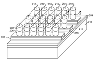
도 2는 소스 평면, 및 그 위에 형성된 복수의 선택기 트랜지스터들 및 자기 메모리 소자들을 갖는 기판의 개략적인 사시도이다;
도 3은 워드 라인, 선택기 트랜지스터, 및 그 위에 형성된 자기 터널 접합 메모리 소자를 도시하는, 도 2의 라인 3-3으로부터 취해진 확대 단면도이다;
도 4는 소스 평면에 연결된 자기 메모리 소자들의 어레이의 개략도이다; 그리고
도 5는 데이터 판독 및 기입 속도를 전압의 함수로서 나타낸 그래프이다.For a more complete understanding of the preferred mode of use as well as the nature and advantages of the present invention, reference should be made to the following detailed description in conjunction with the accompanying drawings, which are not drawn to scale.
1 is a schematic cross-sectional view of a perpendicular magnetic tunnel junction (pMTJ) device;
2 is a schematic perspective view of a substrate having a source plane and a plurality of selector transistors and magnetic memory elements formed thereon;
FIG. 3 is an enlarged cross-sectional view taken from line 3-3 of FIG. 2 showing a word line, a selector transistor, and a magnetic tunnel junction memory element formed thereon;
4 is a schematic diagram of an array of magnetic memory elements coupled to a source plane; and
5 is a graph showing data read and write rates as a function of voltage.
하기의 설명은 본 발명을 수행하기 위해 현재 고려되는 최선의 실시예들에 대한 것이다. 본 설명은 본 발명의 일반적인 원리들을 설명하기 위한 것이고, 본원에서 청구되는 발명의 개념을 제한하려는 것은 아니다.DETAILED DESCRIPTION OF THE PREFERRED EMBODIMENTS The following description is directed to best embodiments currently contemplated for carrying out the present invention. This description is intended to explain the general principles of the invention and is not intended to limit the inventive concept as claimed herein.
이제 도 1을 참조하면, 자기 메모리 소자(100)는 수직 자기 터널 접합(pMTJ) 메모리 소자의 형태일 수 있다. 자기 메모리 소자는 자성 기준층(102), 자성 자유층(104), 및 자성 기준층(102)과 자성 자유층(104) 사이에 위치된 얇은 비자성 전기 절연 배리어 층(106)을 포함할 수 있는 MTJ(101)를 포함할 수 있다. 배리어층(106)은 MgO와 같은 산화물일 수 있다. 자성 기준층은 화살표(108)에 의해 표시된 바와 같이, 바람직하게는 층들의 평면에 수직인 방향으로 고정되게 자화된다(108). 자성 자유층(104)은 층(104)의 평면에 수직인 두 방향 중 어느 하나로 있을 수 있게 자화된다(110). 자유층(104)의 자화(110)는 정지 상태(quiescent state)에서 층(104)의 평면에 수직인 두 방향 중 어느 한 방향으로 유지되지만, 아래에서 더 상세히 설명될 바와 같이, 이들 두 방향 사이에서 가변될 수 있다. 자성 자유층(104)의 자화(110)가 기준층(102)의 자화(108)와 동일한 방향에 있을 때, 층들(102, 106, 104)에 걸친 전기 저항은 저저항 상태에 있다. 반대로, 자유층(104)의 자화(110)가 기준층(102)의 자화(108)의 반대일 때, 층들(102, 106, 104)에 걸친 전기 저항은 고저항 상태에 있다.Referring now to FIG. 1 , the
자성 기준층(102)은 자기 밸런싱 하부층(114), 및 하부 합성 반강자성체(Synthetic Anti-Ferromagnet, SAF)층(114)과 기준층(102) 사이에 위치된 비자성 역평행 커플링층(이를테면, Ru)(116)을 포함할 수 있는 SAF(112)와 같은 역평행 자성 고정(pinning) 구조체의 일부일 수 있다. 아래에서 더 상세히 설명될 역평행 커플링층(116)은 층들(114, 102)을 역평행 구성으로 커플링하도록 하는 조성 및 두께를 갖도록 구성될 수 있다. 층들(114, 102) 간의 역평행 커플링은 기준층(102)의 자화(108)가 하부 SAF 층(114)의 자화 방향(118)과 반대 방향이도록 한다.The
메모리 소자(100)의 하단 부근에는 위에서 퇴적된 층들에서 요구되는 결정 구조를 개시하도록 시드층(120)이 제공될 수 있다. 메모리 소자(100)의 상단 부근에는 그 밑에 있는 층들을 제조 동안, 이를테면 고온 어닐링 동안 그리고 주위 분위기에의 노출로부터 보호하기 위해 캡핑층(121)이 제공될 수 있다. 캡핑층(121)은 예를 들어, Ta로 구성될 수 있다. 또한, 캡핑층(121) 위의 메모리 소자(100)의 상단에는 Ru 하드 마스크층(122)이 형성된다. 선택 사항으로서, Ru층(122)은 하드 마스크층으로서의 역할과 캡핑층(121)으로서의 역할을 모두 할 수 있어, 별도의 캡핑층(122)이 필요하지 않을 수 있다. Ru의 사용은 다른 하드 마스크 물질층 물질에 비해 여러 이점을 제공한다. 예를 들어, Ru 하드 마스크층(122)은 전기 절연 산화물을 형성하지 않고, 이에 따라 다른 하드 마스크 물질을 산화시킬 수 있는 다양한 처리 단계 후에도 양호한 전기 전도체로 남는다. 따라서, Ru 하드 마스크(122)는 기생 저항 없이 완성된 메모리 소자(100)에 남아 있을 수 있다. 또한, Ru는 이온 빔 에칭(이온 밀링으로도 알려져 있음)에 의한 제거에 대해 높은 내성을 갖는다. 이는 유리하게는 하드 마스크층이 얇아질 수 있게 하며, 이는 결과적으로 메모리 소자들의 간격을 줄이고 데이터 밀도를 증가시킬 수 있다. 이러한 Ru 캡핑층(122)의 이점들은 아래에서 더 상세히 설명될 바와 같은 자기 메모리 소자들을 제조하는 다양한 방법과 관련하여 보다 쉽게 이해될 것이다.A
또한, 메모리 소자(100)의 하단 및 상단에는 전극들(124, 126)은 제공될 수 있다. 전극들(124, 126)은 Ta, W, Cu 및 Al 중 하나 이상과 같은 비자성, 전기 전도성 물질로 구성될 수 있으며, 전류원을 포함할 수 있고 메모리 소자(100)에 걸친 전기 저항을 판독하기 위한 CMOS 회로부와 같은 회로부를 더 포함할 수 있는 회로부(128)와의 전기적 연결을 제공할 수 있다.In addition,
자성 자유층(104)은 자유층(104)의 자화(110)가 자유층(104)의 평면에 수직인 두 방향 중 하나로 안정하게 유지되게 하는 수직 자기 이방성(perpendicular magnetic anisotropy)을 갖는다. 기입 모드에서, 자유층(104)의 자화(110)의 배향은 회로부(128)로부터 메모리 소자(100)를 통해 전류를 인가함으로써 이들 두 방향 사이에서 스위칭될 수 있다. 일방향의 전류는 메모리 소자가 제1 배향으로 플립하게 할 것이고, 반대 방향의 전류는 자화가 제2의 반대 방향으로 플립하게 할 것이다. 예를 들어, 자화(110)가 초기에 도 1에서의 하방으로 배향된다면, 소자(100)를 통해 하방으로 전류를 인가하는 것은 전자들이 반대 방향으로, 소자(100)를 통해 상방으로 흐르게 할 것이다. 기준층을 통해 이동한 전자들은 기준층(102)의 자화(108)의 결과로서 스핀 분극될 것이다. 이러한 스핀 분극된 전자들은 자유층(104)의 자화(110)에 스핀 토크를 야기하며, 이는 자화 방향을 플립한다.The magnetic
한편, 자유층(104)의 자화(110)가 초기에 도 1에서의 상방이라면, 소자(100)를 통해 상방으로 전류를 인가하는 것은 전자들이 반대 방향으로, 소자(100)를 통해 하방으로 흐르게 할 것이다. 그러나, 자유층(104)의 자화(110)가 기준층(102)의 자화(108)와 반대이기 때문에, 반대 스핀을 갖는 전자들은 배리어층(106)을 통해 기준층(102)으로 효율적으로 통과할 수 없을 것이다. 그 결과, 반대 스핀을 갖는 전자들은 배리어층(106)에서 반사되고, 기준층(102)의 스핀 분극과 반대의 스핀 분극을 갖는 자유층(104)으로 되돌아갈 것이다. 이러한 스핀 분극된 전자들은 자유층(104)의 자화(110)를 상방으로부터 하방으로 플립하는 스핀 토크를 야기한다.On the other hand, if the
도 2는 전기적 컨택트들(206)을 통해 2차원 평면 소스 라인(204)과 연결된 자기 메모리 소자들의 어레이(202)를 도시한 사시도이다. 워드 라인들(208)은 수직 트랜지스터 채널 선택기들(도 2에 도시되지 않음)을 통해 메모리 소자들(202) 및 컨택트들(206)을 소스 평면(204)과 선택적으로 연결한다. 복수의 전기 전도성 비트 라인들(210)이 소스 평면(204) 및 수직 트랜지스터 채널 선택기의 반대편에 있는 단부에서 메모리 소자들(202)과 전기적으로 연결된다.2 is a perspective view illustrating an
소스 평면(204)은 실리콘(Si)과 같은 반도체 기판일 수 있는 기판(212) 상에 형성된다. 소스 평면(204)은 반도체 기판(212)의 도핑(예를 들어, n-도핑) 층일 수 있는 제1 층(214)을 포함할 수 있다. 소스 평면(204)은 또한, 선택 사항인 제2 층(216)을 포함할 수 있으며, 이는 n-도핑 층(204)에 스트래핑(strapping)되는 전기 전도성 금속일 수 있다. 선택 사항이지만, 제2 전기 전도성 금속층(216)은 메모리 소자들(202)에 기입 전류를 제공하기 위한 추가적인 전기 전도성을 제공한다.The
더 큰 데이터 용량에 대한 요구는 어레이에서 메모리 소자들(202)의 밀도를 증가시키려는 요구로 이어졌다. 이러한 어레이들에서, 이전에는 소스 라인들이 메모리 소자들(202)의 로우 또는 컬럼과 연결하는 2차원 라인들로서 형성되었다. 이러한 소스 라인들은 기판에 (예를 들어, n-도핑된) 도핑 영역을 복수의 라인들로서 형성함으로써 구성되었다. 그러나, 제조 한계 그리고 또한 전기 전도성 및 분리 제한 모두에 의해 이러한 선형 소스 라인들의 밀도가 제한되었다.The demand for greater data capacity has led to a desire to increase the density of
그러나, 본 발명은 개별 패터닝된 선형의 1차원 소스 라인들을 형성하지 않고, 2차원 소스 평면(204)을 통합함으로써 데이터 밀도 증가 가능성을 크게 증가시킨다. 도 3은 메모리 소자(202), 커넥터(206), 워드 라인(208) 및 소스 라인(204)을 보다 상세하게 설명하기 위해 도 2의 라인 3-3으로부터 본 측단면도를 도시한다.However, the present invention greatly increases the possibility of increasing data density by integrating the two-
도 3은 상술한 바와 같이 Si 기판과 같은 반도체 기판일 수 있는 기판(212)을 도시한다. 도핑 층(214)이 기판(212)의 상측 표면에 형성되고, 선택 사항인(그러나 바람직한) 전기 전도성 층(216)이 도핑 층(214)(과 스트래핑되어) 위에 형성될 수 있다. 전기 전도성 금속층(216)은 스퍼터 퇴적과 같은 공정에 의해 퇴적될 수 있다. 수직 반도체 채널 구조체가 소스 평면층(304) 위에 형성된다. 수직 채널 구조체는 수직 반도체 컬럼(308)(바람직하게는 Si)을 포함하며, 반도체 컬럼(308)의 상측 및 하측 단부들에 소스 및 드레인 영역들을 갖는다. 반도체 칼럼(308)은 그 외측면이 게이트 유전체 층(302) - 이는 SiO2 또는 NiOx와 같은 산화물 또는 질화물 층일 수 있음 - 에 의해 둘러싸인다. 게이트 유전체 층(302)이 반도체 컬럼(308)으로부터 게이트 라인(208)을 분리하도록, 게이트 라인(208)이 반도체 컬럼(308) 및 게이트 유전체(302)에 인접하여 형성된다. 게이트 라인(208)은 n-도핑된 Si와 같은 n-도핑된 반도체 층일 수 있거나, 또는 금속과 같은 전기 전도성 물질일 수도 있다. 게이트 라인(208)의 하단에 형성되는 유전체 층(304)은 게이트 라인을 아래에 놓인 소스 라인층(204)으로부터 분리시킨다. 유전체 층(304)은 SiO2 또는 NiOx와 같은 산화물 또는 질화물일 수 있다. 또 다른 유전체 층(306)이 게이트 라인(208)을 주변 구조체들로부터 전기적으로 격리시키기 위해 게이트 라인(208)의 상단에 형성될 수 있다. 상측 유전체 층은 SiO2 또는 SiNx와 같은 산화물 또는 질화물일 수 있다. 반도체 컬럼(308)은 에피택셜 성장에 의해 형성될 수 있거나, 또는 다결정 반도체(예를 들어, 다결정 Si)의 퇴적에 이어서 어닐링 공정에 의해 형성될 수 있다. 반도체 컬럼(308)의 상측 및 하측 부분들은 도핑되어 반도체 컬럼(308)의 소스 및 드레인 영역들을 형성할 수 있다.3 shows a
자기 메모리 소자(202)는 반도체 컬럼(308) 위에 형성될 수 있다. 하단 전극(312)이 메모리 소자(202)의 하단에 형성되어 메모리 소자(202)와 반도체 칼럼(308) 사이에 전기적 연결을 제공할 수 있다. 하단 전극(312)은 TaN과 같은 전기 전도성 금속으로 형성될 수 있다. 추가적인 전기 전도성 컨택트 구조체들(도시되지 않음)이 메모리 소자(202)와 반도체 칼럼(308) 사이에, 이를테면 하단 전극(312)과 반도체 칼럼(308) 사이에 제공될 수 있다. 상단 전극(314)이 메모리 소자(202)의 상단에 형성되어 도 2를 참조하여 전술된 비트 라인(210)과 메모리 소자(202) 사이에 전기적 연결을 제공할 수 있다. 상단 전극(314)은 TaN과 같은 물질로 형성될 수 있고, 상단 전극과 메모리 소자(202)의 구성을 위한 하드 마스크 모두로서 기능할 수 있다. 비트 라인(210)은 전기 전도성의, 비자성 금속일 수 있다. 유전체 격리층(310)이 메모리 소자(202)를 둘러싸도록 메모리 소자(202)의 측면에 형성되어 메모리 소자(202)와 어레이에서의 다른 인접한 메모리 소자들 사이에 전기적 격리를 제공할 수 있다. 유전체 격리층(310)은 SiOx 또는 SiNx와 같은 하나 이상의 산화물 또는 질화물 층으로 구성될 수 있다.The
자기 메모리 소자(202)는 자기 터널 접합(MTJ)일 수 있다. 자기 메모리 소자(202)는 도 1을 참조하여 상술된 MTJ 구조체(100)와 같은 구조체를 가질 수 있거나, 또는 일부 다른 적절한 구조체를 가질 수 있다. 자기 메모리 소자(202)에 데이터를 기입하기 위해, 전류가 소스 평면(204)과 비트 라인(210) 사이에서 메모리 소자에 인가된다. 메모리 소자(202)를 통한 전류 흐름의 방향은 메모리 소자가 고저항 역평행 자기 상태로 스위칭될 것인지 또는 저저항 평행 자기 상태로 스위칭될 것인지를 결정한다. 메모리 소자로부터 데이터 비트를 판독하기 위해, 판독 전류(기입 전류보다 작음)가 비트 라인(210)과 소스 평면(204) 사이에서 메모리 소자(202)에 걸쳐 인가된다. 게이트 라인(208) 및 게이트 유전체(302)를 함께 둘러싸는 반도체 컬럼(308)은 기입 전류를 메모리 소자에 선택적으로 인가하기 위한 트랜지스터 선택기를 제공한다. 전압이 게이트 층(208)에 인가될 때, 트랜지스터는 스위치 온되어, 전류가 반도체 채널(308)을 통해 흐를 수 있게 한다. 게이트 층(208)은 메모리 어레이의 워드 라인의 일부이거나 이와 연결될 수 있다.The
도 4는 소스 평면을 통합하는 메모리 어레이(400)의 전기 배선도를 도시한다. 어레이(400)는 로우들(R0, R1 … Rx), 및 컬럼들(C0, C1, C2 … Cx)로 배열된 복수의 자기 메모리 소자들(402)을 포함한다. 자기 메모리 소자들(202) 각각은 일단부(예를 들어, 하단부)에서 채널 선택기(204)와 연결되며, 이는 전술된 도 3의 구성과 유사한 구성을 가질 수 있다. 각 채널 선택기(204)는 관련 자기 메모리 소자를 소스 평면(VSP)(206)과 선택적으로 연결한다. 채널 선택기는 메모리 소자(202)에 소스 평면 전압을 인가하거나 메모리 소자 (202)를 소스 평면(206)으로부터 연결 해제시키는 스위치로서 기능한다. 채널 선택기들(204) 각각은 워드 라인 - 이는 채널 선택기에 게이트 전압을 인가하여 채널 선택기를 "온" 상태로 전환시키거나 또는 게이트 전압을 제거하여 채널 선택기(204)를 "오프" 상태로 전환시키는 기능을 함 - 과 연결된다.4 shows an electrical schematic of a
도 4를 계속 참조하면, 하나 이상의 비트 라인 I/O 멀티플렉서(210)가 메모리 소자들의 하나 이상의 컬럼과 연결된다. 비트 라인 전압은 소스 평면 전압이 연결되는 단부의 반대편에 있는 그 각각의 메모리 소자(202)의 단부에 인가된다. 복수의 비트 라인 채널 선택기들(트랜지스터들)(212)은 비트 라인 전압이 인가되는 메모리 소자(202)의 컬럼(C0 … Cx)을 선택하기 위해 제공될 수 있다.With continued reference to FIG. 4 , one or more bit line I/
소스 평면들(206)은 어레이에서의 모든 메모리 소자/채널 선택기 조합들(202, 204) 모두에 연결되는 2차원 소스 평면 - 이는 도 2 및 도 3을 참조하여 상술된 평면 구조체(204) 형태일 수 있음 - 을 개략적으로 나타낸다는 것을 거듭 언급한다. 특정 메모리 소자(202)의 선택은 관련 워드 라인(208)으로부터의 전압에 의해 활성화되는 관련 채널 선택기를 통한 소스 평면 전압의 제어된 인가에 의해, 그리고 관련 비트 라인 채널 선택기(212)의 활성화를 통한 비트 라인 전압의 인가에 의해 제공된다.The source planes 206 are a two-dimensional source plane that connects to all of all memory element/
또한, 소스 평면(206)은 소스 평면 전압원(214)과 연결될 수 있거나, 또는 대안적으로 접지와 연결될 수 있다는 것을 주목해야 한다. 메모리 소자(202)의 메모리 상태를 스위칭하기에 충분한 전류를 메모리 소자를 통해 제공하는 데 필요한 전압은 스위칭 전압(VSW)으로서 지칭된다. 소스 평면 전압은 VSW 이상이어야 한다. 도 5를 참조한다. 비트 라인들에 대한 공급 전압인 VDD는 2x VSW 이상이어야 한다. VSP는 필요에 따라 "1"들 또는 "0"들 중 어느 하나를 기입하기 위해 더 높은 스위칭 전압을 제공하도록 조정될 수 있다. 따라서, 개별 메모리 소자(202)에 기입할 때, 메모리 소자(202)에 인가되는 순 전압의 양은 적어도 스위칭 전압(Vsw)과 동일해야 한다. 소스 평면(206)이 전압원(214)과 연결된다면, 그 전압원은 적어도 Vsw와 동일한 전압(VSP)을 제공한다. 한 방향으로 기입하기 위해, 관련 채널 선택기(204)는 개방되고, 소스 전압은 전압(VSP)을 인가하며, 비트 라인은 제로 전압을 제공한다. 따라서, 이러한 경우에, (예를 들어, 메모리 소자(202)를 통해 상방으로의) 전압(VSP)은 메모리 소자의 메모리 상태를 스위칭하기에 충분하다. 메모리 소자를 반대 상태로 스위칭하기 위해, 비트 라인은 적어도 2(Vsw) 또는 소스 전압의 두 배인 전압을 제공하도록 구성된다. 이 경우, 메모리 소자를 통한 순 전압은 반대 방향으로의 VSP가 될 것이며, 이에 의해 반대 방향으로의 스위칭을 제공할 수 있다.It should also be noted that the
한편, 소스 평면(206)이 접지에 연결된다면, 유효 전압을 제공하지 않을 것이다. 이러한 경우, 비트 라인 및 관련 회로부는 요구되는 자기 상태에 따라 양 또는 음 중 어느 하나인 비트 라인 전압을 제공하도록 구성된다. 비트 라인은 +VSP 또는 -VSP의 전압을 제공하도록 구성될 것이며, 여기서 VSP의 절대값은 스위칭 전압(Vsw) 이상이다.On the other hand, if the
도 5는 상술한 바와 같은 메모리 어레이에서의 메모리 소자에 대한 스위칭 특성들의 그래프를 도시하고, 또한 "1"과 "0" 메모리 상태 사이의 스위칭과 연관된 전류를 도시하는 개별 메모리 소자의 개략도를 도시한다. 라인(502)은 자기 센서(202)를 통한 전류의 흐름을 가능하게 하기 위해 도 2, 도 3 및 도 4에 도시된 채널 선택기(206)를 개방하도록 인가되는 워드 라인 전압을 나타낸다. 라인(504)은 비트 라인 전압이고, 라인(506)은 (메모리 소자를 평행 자기 상태로부터 역평행 자기 상태로 스위칭하여) "0" 메모리 상태를 기입할 때 컬럼 어드레스 선택 0(CS0)이다. 이 경우, 소스 평면은 VSP 전압으로 유지되고, 비트 라인은 저전압을 갖는다. 이는 화살표(505)에 의해 표시된 바와 같이 메모리 소자(202)를 통해 상방으로 전류가 흐를 수 있게 함으로써, 메모리 소자(202)가 저저항 역평행 상태로부터 고저항 역평행 상태로 스위칭하게 한다.5 shows a graph of switching characteristics for a memory element in a memory array as described above, and also shows a schematic diagram of an individual memory element showing the current associated with switching between a “1” and a “0” memory state. .
한편, 그래프의 라인(508)은 BL0(504)가 VSP 전압으로 되돌아가는 것을 도시하고, 라인(510)은 역평행 상태로부터 평행 자기 상태로("1"에서 "0"으로) 스위칭할 때 비트 라인 1(BL1) 전압을 나타낸다. 이들 전압 곡선들은 붙어 있는 배선도 상의 화살표(512)에 대응하며, 여기서 하방의 전류는 메모리 소자를 역평행 고저항("1") 상태로부터 평행 저저항("0") 상태로 스위칭한다.On the other hand,
워드 라인(WL)은 음의 전압 VNWL(약 -0.2V 내지 -0.7V)에서 시작한다. 음의 게이트 전압의 목적은 액세스 트랜지스터의 문턱 이하의 누설 전류를 감소시키는 것이다. WL은 메모리 셀에 액세스하기 위해, VPP 전압 - 이는 VDD에 액세스 트랜지스터의 VT의 1배 또는 2배보다 큰 전압을 더한 것보다 큼 - 으로 구동된다. 모든 비트 라인들은 초기에 VSP 전압으로 사전 충전된다. 소스 평면은 선택된 비트 라인 전압에 따라 전류를 공급하거나 싱크(sink)하기 위한 파워 평면이다. VSP는 대략 1/2 VDD 전압의 일정한 공급이다. 비트 라인 전압이 VDD로 구동된다면, 화살표(512)에 의해 표시된 바와 같이, 전류는 비트 라인으로부터 MTJ(202) 및 액세스 트랜지스터(513)를 통해 소스 평면으로 흐를 것이다. 비트 라인이 VSS로 구동된다면, 전류는 화살표(505)에 의해 표시된 바와 같이, 소스 평면으로부터 액세스 트랜지스터(513) 및 MTJ(202)를 통해 비트 라인으로 흐를 것이다. 도 5의 파형은 비트 라인 0(BL0, 504)이 로우로 구동되어 컬럼 어드레스 선택 0(CS0)에 논리 "1"(평행에서 역평행)을 기입하는 것을 도시한다. 다음으로, 비트 라인 1(BL1, 510)은 하이로 구동되어 컬럼 어드레스 선택 1(CS1, 508)에 논리 "0"(역평행에서 평행)을 기입한다. 기입 후, 비트 라인들은 VSP로 사전 충전된다. 컬럼 어드레스 라인들은 선택 해제되고 VSS로 구동된다. 그 다음, WL은 오프로 전환되어 VNWL로 구동된다.The word line WL starts at a negative voltage V NWL (about -0.2V to -0.7V). The purpose of the negative gate voltage is to reduce the subthreshold leakage current of the access transistor. WL is driven with the V PP voltage, which is greater than V DD plus a voltage greater than one or two times the V T of the access transistor, to access the memory cell. All bit lines are initially precharged to the V SP voltage. The source plane is the power plane for supplying or sinking current depending on the selected bit line voltage. V SP is a constant supply of approximately 1/2 V DD voltage. If the bit line voltage is driven to V DD , then current will flow from the bit line through the
다양한 실시예들이 상술되었지만, 이것들은 제한이 아닌 단지 예로서 제시되었다는 것이 이해되어야 한다. 또한, 본 발명의 범위 내에 있는 다른 실시예들도 당업자들에게 명백하게 될 수 있다. 따라서, 본 발명의 외연 및 범위는 상술된 예시적인 실시예들 중 어느 것에 의해서도 제한되어서는 안 되며, 다음의 청구항들 및 그 균등물들에 따라서만 정의되어야 한다. While various embodiments have been described above, it should be understood that these have been presented by way of example only and not limitation. In addition, other embodiments within the scope of the present invention may become apparent to those skilled in the art. Accordingly, the scope and scope of the present invention should not be limited by any of the above-described exemplary embodiments, but should be defined only in accordance with the following claims and their equivalents.
Claims (19)
전기 전도성 소스 평면;
수직 반도체 채널 구조체들의 어레이; 및
복수의 자기 메모리 소자들 - 상기 자기 메모리 소자들 각각은 상기 수직 반도체 채널 구조체들 중 하나에 전기적으로 연결됨 - 을 포함하되,
상기 수직 반도체 채널 구조체들은 2차원으로 상기 소스 평면 상에 형성되고 상기 소스 평면과 연결되는 것인, 자기 메모리 어레이.A magnetic memory array comprising:
electrically conductive source plane;
an array of vertical semiconductor channel structures; and
a plurality of magnetic memory elements, each of the magnetic memory elements electrically coupled to one of the vertical semiconductor channel structures;
and the vertical semiconductor channel structures are formed on and connected to the source plane in two dimensions.
로우들 및 컬럼들로 배열된 채널 선택기들의 2차원 어레이;
로우 및 컬럼 방향 모두에서 상기 채널 선택기들의 2차원 어레이와 전기적으로 연결되는 2차원 소스 평면; 및
상기 채널 선택기들의 2차원 어레이 상에 형성되는 복수의 자기 메모리 소자 구조체들을 포함하는, 자기 메모리 어레이.A magnetic memory array comprising:
a two-dimensional array of channel selectors arranged in rows and columns;
a two-dimensional source plane in electrical communication with the two-dimensional array of channel selectors in both row and column directions; and
and a plurality of magnetic memory device structures formed on the two-dimensional array of channel selectors.
복수의 전기 전도성 워드 라인들 - 각 전기 전도성 워드 라인이 상기 채널 구조체들의 로우와 전기적으로 연결됨 -; 및
복수의 비트 라인들 - 상기 비트 라인들 각각은 자기 메모리 요소들의 컬럼과 전기적으로 연결되고, 상기 컬럼은 상기 로우와 대체로 직교함 - 을 더 포함하는, 자기 메모리 어레이.13. The method of claim 12,
a plurality of electrically conductive word lines, each electrically conductive word line electrically connected with the row of channel structures; and
and a plurality of bit lines, each of said bit lines electrically coupled with a column of magnetic memory elements, said column being generally orthogonal to said row.
Applications Claiming Priority (3)
| Application Number | Priority Date | Filing Date | Title |
|---|---|---|---|
| US16/457,544 | 2019-06-28 | ||
| US16/457,544 US10840298B1 (en) | 2019-06-28 | 2019-06-28 | Vertical selector STT-MRAM architecture |
| PCT/US2020/039897 WO2020264349A1 (en) | 2019-06-28 | 2020-06-26 | Vertical selector stt-mram architecture |
Publications (2)
| Publication Number | Publication Date |
|---|---|
| KR20220010551A true KR20220010551A (en) | 2022-01-25 |
| KR102623306B1 KR102623306B1 (en) | 2024-01-09 |
Family
ID=73264209
Family Applications (1)
| Application Number | Title | Priority Date | Filing Date |
|---|---|---|---|
| KR1020217041572A Active KR102623306B1 (en) | 2019-06-28 | 2020-06-26 | Vertical Selector STT-MRAM Architecture |
Country Status (4)
| Country | Link |
|---|---|
| US (1) | US10840298B1 (en) |
| KR (1) | KR102623306B1 (en) |
| CN (1) | CN113767482B (en) |
| WO (1) | WO2020264349A1 (en) |
Families Citing this family (1)
| Publication number | Priority date | Publication date | Assignee | Title |
|---|---|---|---|---|
| KR102931169B1 (en) | 2021-05-27 | 2026-02-27 | 삼성전자주식회사 | Magnetic memory device |
Citations (3)
| Publication number | Priority date | Publication date | Assignee | Title |
|---|---|---|---|---|
| KR20120034045A (en) * | 2010-09-30 | 2012-04-09 | 시게이트 테크놀로지 엘엘씨 | Vertical transistor stram array |
| KR20140077500A (en) * | 2012-12-14 | 2014-06-24 | 에스케이하이닉스 주식회사 | Vertical Type Semiconductor Device and Fabrication Method Thereof |
| US20160268500A1 (en) * | 2015-03-09 | 2016-09-15 | Kabushiki Kaisha Toshiba | Resistance change memory |
Family Cites Families (4)
| Publication number | Priority date | Publication date | Assignee | Title |
|---|---|---|---|---|
| US8437192B2 (en) * | 2010-05-21 | 2013-05-07 | Macronix International Co., Ltd. | 3D two bit-per-cell NAND flash memory |
| US8168506B2 (en) | 2010-07-13 | 2012-05-01 | Crossbar, Inc. | On/off ratio for non-volatile memory device and method |
| KR20130095499A (en) * | 2012-02-20 | 2013-08-28 | 에스케이하이닉스 주식회사 | Nonvolatile memory device, method for operating the same and method for fabricating the same |
| US9972640B1 (en) * | 2016-11-17 | 2018-05-15 | Sandisk Technologies Llc | Three-dimensional memory device with self-aligned drain side select gate electrodes and method of making thereof |
-
2019
- 2019-06-28 US US16/457,544 patent/US10840298B1/en active Active
-
2020
- 2020-06-26 KR KR1020217041572A patent/KR102623306B1/en active Active
- 2020-06-26 CN CN202080031754.7A patent/CN113767482B/en active Active
- 2020-06-26 WO PCT/US2020/039897 patent/WO2020264349A1/en not_active Ceased
Patent Citations (3)
| Publication number | Priority date | Publication date | Assignee | Title |
|---|---|---|---|---|
| KR20120034045A (en) * | 2010-09-30 | 2012-04-09 | 시게이트 테크놀로지 엘엘씨 | Vertical transistor stram array |
| KR20140077500A (en) * | 2012-12-14 | 2014-06-24 | 에스케이하이닉스 주식회사 | Vertical Type Semiconductor Device and Fabrication Method Thereof |
| US20160268500A1 (en) * | 2015-03-09 | 2016-09-15 | Kabushiki Kaisha Toshiba | Resistance change memory |
Also Published As
| Publication number | Publication date |
|---|---|
| CN113767482B (en) | 2024-08-13 |
| KR102623306B1 (en) | 2024-01-09 |
| WO2020264349A1 (en) | 2020-12-30 |
| US10840298B1 (en) | 2020-11-17 |
| CN113767482A (en) | 2021-12-07 |
Similar Documents
| Publication | Publication Date | Title |
|---|---|---|
| US12389607B2 (en) | Bipolar selector with independently tunable threshold voltages | |
| US6946712B2 (en) | Magnetic memory device using SOI substrate | |
| US11469371B2 (en) | SOT-MRAM cell in high density applications | |
| US20030123271A1 (en) | Magnetic random access memory | |
| US6838721B2 (en) | Integrated circuit with a transitor over an interconnect layer | |
| JP7700239B2 (en) | High-density spin-orbit magnetic random access memory | |
| TW202147650A (en) | Magnetic memory device | |
| US6798689B2 (en) | Integrated memory with a configuration of non-volatile memory cells and method for fabricating and for operating the integrated memory | |
| US11468932B2 (en) | Magnetic memory device with write current flowing simultaneously through non-adjacent lines in memory cell array | |
| JP2004273918A (en) | Magnetic random access memory and method of manufacturing the same | |
| KR102623306B1 (en) | Vertical Selector STT-MRAM Architecture | |
| KR100979350B1 (en) | Magnetic ram and method of manufacturing the same | |
| US10854255B1 (en) | Vertical selector stt-MRAM architecture | |
| JP2003209228A (en) | Magnetic storage device and method of manufacturing the same | |
| US9030867B2 (en) | Bipolar CMOS select device for resistive sense memory | |
| US10453895B2 (en) | Magnetic memory device with a common source having an array of openings, system, and method of fabrication | |
| JP4000000B2 (en) | Magnetic random access memory and manufacturing method thereof | |
| WO2025063191A1 (en) | Semiconductor storage device, method for manufacturing semiconductor storage device, writing method, reading method, and storage system | |
| JP2003092390A (en) | Magnetoresistive memory device and method of manufacturing the same | |
| KR20250159673A (en) | STT-assisted SOT write-based magnetic memory cell including N-type transistor and P-type transistor as select transistors, and MRAM memory | |
| CN105518892A (en) | Nonvolatile Memory Devices Using Thin Film Transistors and Schottky Diodes | |
| WO2024108879A1 (en) | Memory, read-write method of memory, and manufacturing method for memory |
Legal Events
| Date | Code | Title | Description |
|---|---|---|---|
| PA0105 | International application |
Patent event date: 20211217 Patent event code: PA01051R01D Comment text: International Patent Application |
|
| PA0201 | Request for examination | ||
| PG1501 | Laying open of application | ||
| E902 | Notification of reason for refusal | ||
| PE0902 | Notice of grounds for rejection |
Comment text: Notification of reason for refusal Patent event date: 20230526 Patent event code: PE09021S01D |
|
| E701 | Decision to grant or registration of patent right | ||
| PE0701 | Decision of registration |
Patent event code: PE07011S01D Comment text: Decision to Grant Registration Patent event date: 20231106 |
|
| GRNT | Written decision to grant | ||
| PR0701 | Registration of establishment |
Comment text: Registration of Establishment Patent event date: 20240105 Patent event code: PR07011E01D |
|
| PR1002 | Payment of registration fee |
Payment date: 20240105 End annual number: 3 Start annual number: 1 |
|
| PG1601 | Publication of registration |