KR20210106051A - Displya device - Google Patents
Displya device Download PDFInfo
- Publication number
- KR20210106051A KR20210106051A KR1020200020310A KR20200020310A KR20210106051A KR 20210106051 A KR20210106051 A KR 20210106051A KR 1020200020310 A KR1020200020310 A KR 1020200020310A KR 20200020310 A KR20200020310 A KR 20200020310A KR 20210106051 A KR20210106051 A KR 20210106051A
- Authority
- KR
- South Korea
- Prior art keywords
- block
- value
- transistor
- sensing
- values
- Prior art date
- Legal status (The legal status is an assumption and is not a legal conclusion. Google has not performed a legal analysis and makes no representation as to the accuracy of the status listed.)
- Granted
Links
Images


Classifications
-
- G—PHYSICS
- G09—EDUCATION; CRYPTOGRAPHY; DISPLAY; ADVERTISING; SEALS
- G09G—ARRANGEMENTS OR CIRCUITS FOR CONTROL OF INDICATING DEVICES USING STATIC MEANS TO PRESENT VARIABLE INFORMATION
- G09G3/00—Control arrangements or circuits, of interest only in connection with visual indicators other than cathode-ray tubes
- G09G3/20—Control arrangements or circuits, of interest only in connection with visual indicators other than cathode-ray tubes for presentation of an assembly of a number of characters, e.g. a page, by composing the assembly by combination of individual elements arranged in a matrix no fixed position being assigned to or needed to be assigned to the individual characters or partial characters
- G09G3/2003—Display of colours
-
- G—PHYSICS
- G09—EDUCATION; CRYPTOGRAPHY; DISPLAY; ADVERTISING; SEALS
- G09G—ARRANGEMENTS OR CIRCUITS FOR CONTROL OF INDICATING DEVICES USING STATIC MEANS TO PRESENT VARIABLE INFORMATION
- G09G3/00—Control arrangements or circuits, of interest only in connection with visual indicators other than cathode-ray tubes
- G09G3/20—Control arrangements or circuits, of interest only in connection with visual indicators other than cathode-ray tubes for presentation of an assembly of a number of characters, e.g. a page, by composing the assembly by combination of individual elements arranged in a matrix no fixed position being assigned to or needed to be assigned to the individual characters or partial characters
- G09G3/22—Control arrangements or circuits, of interest only in connection with visual indicators other than cathode-ray tubes for presentation of an assembly of a number of characters, e.g. a page, by composing the assembly by combination of individual elements arranged in a matrix no fixed position being assigned to or needed to be assigned to the individual characters or partial characters using controlled light sources
- G09G3/28—Control arrangements or circuits, of interest only in connection with visual indicators other than cathode-ray tubes for presentation of an assembly of a number of characters, e.g. a page, by composing the assembly by combination of individual elements arranged in a matrix no fixed position being assigned to or needed to be assigned to the individual characters or partial characters using controlled light sources using luminous gas-discharge panels, e.g. plasma panels
-
- G—PHYSICS
- G09—EDUCATION; CRYPTOGRAPHY; DISPLAY; ADVERTISING; SEALS
- G09G—ARRANGEMENTS OR CIRCUITS FOR CONTROL OF INDICATING DEVICES USING STATIC MEANS TO PRESENT VARIABLE INFORMATION
- G09G3/00—Control arrangements or circuits, of interest only in connection with visual indicators other than cathode-ray tubes
- G09G3/20—Control arrangements or circuits, of interest only in connection with visual indicators other than cathode-ray tubes for presentation of an assembly of a number of characters, e.g. a page, by composing the assembly by combination of individual elements arranged in a matrix no fixed position being assigned to or needed to be assigned to the individual characters or partial characters
- G09G3/2092—Details of a display terminals using a flat panel, the details relating to the control arrangement of the display terminal and to the interfaces thereto
-
- G—PHYSICS
- G09—EDUCATION; CRYPTOGRAPHY; DISPLAY; ADVERTISING; SEALS
- G09G—ARRANGEMENTS OR CIRCUITS FOR CONTROL OF INDICATING DEVICES USING STATIC MEANS TO PRESENT VARIABLE INFORMATION
- G09G3/00—Control arrangements or circuits, of interest only in connection with visual indicators other than cathode-ray tubes
- G09G3/006—Electronic inspection or testing of displays and display drivers, e.g. of LED or LCD displays
-
- G—PHYSICS
- G09—EDUCATION; CRYPTOGRAPHY; DISPLAY; ADVERTISING; SEALS
- G09G—ARRANGEMENTS OR CIRCUITS FOR CONTROL OF INDICATING DEVICES USING STATIC MEANS TO PRESENT VARIABLE INFORMATION
- G09G3/00—Control arrangements or circuits, of interest only in connection with visual indicators other than cathode-ray tubes
- G09G3/20—Control arrangements or circuits, of interest only in connection with visual indicators other than cathode-ray tubes for presentation of an assembly of a number of characters, e.g. a page, by composing the assembly by combination of individual elements arranged in a matrix no fixed position being assigned to or needed to be assigned to the individual characters or partial characters
- G09G3/2085—Special arrangements for addressing the individual elements of the matrix, other than by driving respective rows and columns in combination
-
- G—PHYSICS
- G09—EDUCATION; CRYPTOGRAPHY; DISPLAY; ADVERTISING; SEALS
- G09G—ARRANGEMENTS OR CIRCUITS FOR CONTROL OF INDICATING DEVICES USING STATIC MEANS TO PRESENT VARIABLE INFORMATION
- G09G3/00—Control arrangements or circuits, of interest only in connection with visual indicators other than cathode-ray tubes
- G09G3/20—Control arrangements or circuits, of interest only in connection with visual indicators other than cathode-ray tubes for presentation of an assembly of a number of characters, e.g. a page, by composing the assembly by combination of individual elements arranged in a matrix no fixed position being assigned to or needed to be assigned to the individual characters or partial characters
- G09G3/22—Control arrangements or circuits, of interest only in connection with visual indicators other than cathode-ray tubes for presentation of an assembly of a number of characters, e.g. a page, by composing the assembly by combination of individual elements arranged in a matrix no fixed position being assigned to or needed to be assigned to the individual characters or partial characters using controlled light sources
- G09G3/30—Control arrangements or circuits, of interest only in connection with visual indicators other than cathode-ray tubes for presentation of an assembly of a number of characters, e.g. a page, by composing the assembly by combination of individual elements arranged in a matrix no fixed position being assigned to or needed to be assigned to the individual characters or partial characters using controlled light sources using electroluminescent panels
- G09G3/32—Control arrangements or circuits, of interest only in connection with visual indicators other than cathode-ray tubes for presentation of an assembly of a number of characters, e.g. a page, by composing the assembly by combination of individual elements arranged in a matrix no fixed position being assigned to or needed to be assigned to the individual characters or partial characters using controlled light sources using electroluminescent panels semiconductive, e.g. using light-emitting diodes [LED]
- G09G3/3208—Control arrangements or circuits, of interest only in connection with visual indicators other than cathode-ray tubes for presentation of an assembly of a number of characters, e.g. a page, by composing the assembly by combination of individual elements arranged in a matrix no fixed position being assigned to or needed to be assigned to the individual characters or partial characters using controlled light sources using electroluminescent panels semiconductive, e.g. using light-emitting diodes [LED] organic, e.g. using organic light-emitting diodes [OLED]
- G09G3/3225—Control arrangements or circuits, of interest only in connection with visual indicators other than cathode-ray tubes for presentation of an assembly of a number of characters, e.g. a page, by composing the assembly by combination of individual elements arranged in a matrix no fixed position being assigned to or needed to be assigned to the individual characters or partial characters using controlled light sources using electroluminescent panels semiconductive, e.g. using light-emitting diodes [LED] organic, e.g. using organic light-emitting diodes [OLED] using an active matrix
- G09G3/3233—Control arrangements or circuits, of interest only in connection with visual indicators other than cathode-ray tubes for presentation of an assembly of a number of characters, e.g. a page, by composing the assembly by combination of individual elements arranged in a matrix no fixed position being assigned to or needed to be assigned to the individual characters or partial characters using controlled light sources using electroluminescent panels semiconductive, e.g. using light-emitting diodes [LED] organic, e.g. using organic light-emitting diodes [OLED] using an active matrix with pixel circuitry controlling the current through the light-emitting element
-
- G—PHYSICS
- G09—EDUCATION; CRYPTOGRAPHY; DISPLAY; ADVERTISING; SEALS
- G09G—ARRANGEMENTS OR CIRCUITS FOR CONTROL OF INDICATING DEVICES USING STATIC MEANS TO PRESENT VARIABLE INFORMATION
- G09G3/00—Control arrangements or circuits, of interest only in connection with visual indicators other than cathode-ray tubes
- G09G3/20—Control arrangements or circuits, of interest only in connection with visual indicators other than cathode-ray tubes for presentation of an assembly of a number of characters, e.g. a page, by composing the assembly by combination of individual elements arranged in a matrix no fixed position being assigned to or needed to be assigned to the individual characters or partial characters
- G09G3/34—Control arrangements or circuits, of interest only in connection with visual indicators other than cathode-ray tubes for presentation of an assembly of a number of characters, e.g. a page, by composing the assembly by combination of individual elements arranged in a matrix no fixed position being assigned to or needed to be assigned to the individual characters or partial characters by control of light from an independent source
- G09G3/36—Control arrangements or circuits, of interest only in connection with visual indicators other than cathode-ray tubes for presentation of an assembly of a number of characters, e.g. a page, by composing the assembly by combination of individual elements arranged in a matrix no fixed position being assigned to or needed to be assigned to the individual characters or partial characters by control of light from an independent source using liquid crystals
- G09G3/3611—Control of matrices with row and column drivers
- G09G3/3648—Control of matrices with row and column drivers using an active matrix
-
- G—PHYSICS
- G09—EDUCATION; CRYPTOGRAPHY; DISPLAY; ADVERTISING; SEALS
- G09G—ARRANGEMENTS OR CIRCUITS FOR CONTROL OF INDICATING DEVICES USING STATIC MEANS TO PRESENT VARIABLE INFORMATION
- G09G2320/00—Control of display operating conditions
- G09G2320/02—Improving the quality of display appearance
- G09G2320/029—Improving the quality of display appearance by monitoring one or more pixels in the display panel, e.g. by monitoring a fixed reference pixel
- G09G2320/0295—Improving the quality of display appearance by monitoring one or more pixels in the display panel, e.g. by monitoring a fixed reference pixel by monitoring each display pixel
-
- G—PHYSICS
- G09—EDUCATION; CRYPTOGRAPHY; DISPLAY; ADVERTISING; SEALS
- G09G—ARRANGEMENTS OR CIRCUITS FOR CONTROL OF INDICATING DEVICES USING STATIC MEANS TO PRESENT VARIABLE INFORMATION
- G09G2320/00—Control of display operating conditions
- G09G2320/04—Maintaining the quality of display appearance
- G09G2320/043—Preventing or counteracting the effects of ageing
-
- G—PHYSICS
- G09—EDUCATION; CRYPTOGRAPHY; DISPLAY; ADVERTISING; SEALS
- G09G—ARRANGEMENTS OR CIRCUITS FOR CONTROL OF INDICATING DEVICES USING STATIC MEANS TO PRESENT VARIABLE INFORMATION
- G09G2330/00—Aspects of power supply; Aspects of display protection and defect management
- G09G2330/02—Details of power systems and of start or stop of display operation
- G09G2330/021—Power management, e.g. power saving
-
- G—PHYSICS
- G09—EDUCATION; CRYPTOGRAPHY; DISPLAY; ADVERTISING; SEALS
- G09G—ARRANGEMENTS OR CIRCUITS FOR CONTROL OF INDICATING DEVICES USING STATIC MEANS TO PRESENT VARIABLE INFORMATION
- G09G2330/00—Aspects of power supply; Aspects of display protection and defect management
- G09G2330/02—Details of power systems and of start or stop of display operation
- G09G2330/025—Reduction of instantaneous peaks of current
-
- G—PHYSICS
- G09—EDUCATION; CRYPTOGRAPHY; DISPLAY; ADVERTISING; SEALS
- G09G—ARRANGEMENTS OR CIRCUITS FOR CONTROL OF INDICATING DEVICES USING STATIC MEANS TO PRESENT VARIABLE INFORMATION
- G09G2330/00—Aspects of power supply; Aspects of display protection and defect management
- G09G2330/04—Display protection
- G09G2330/045—Protection against panel overheating
-
- G—PHYSICS
- G09—EDUCATION; CRYPTOGRAPHY; DISPLAY; ADVERTISING; SEALS
- G09G—ARRANGEMENTS OR CIRCUITS FOR CONTROL OF INDICATING DEVICES USING STATIC MEANS TO PRESENT VARIABLE INFORMATION
- G09G2330/00—Aspects of power supply; Aspects of display protection and defect management
- G09G2330/12—Test circuits or failure detection circuits included in a display system, as permanent part thereof
-
- G—PHYSICS
- G09—EDUCATION; CRYPTOGRAPHY; DISPLAY; ADVERTISING; SEALS
- G09G—ARRANGEMENTS OR CIRCUITS FOR CONTROL OF INDICATING DEVICES USING STATIC MEANS TO PRESENT VARIABLE INFORMATION
- G09G2360/00—Aspects of the architecture of display systems
- G09G2360/16—Calculation or use of calculated indices related to luminance levels in display data
Landscapes
- Engineering & Computer Science (AREA)
- Physics & Mathematics (AREA)
- Computer Hardware Design (AREA)
- General Physics & Mathematics (AREA)
- Theoretical Computer Science (AREA)
- Chemical & Material Sciences (AREA)
- Crystallography & Structural Chemistry (AREA)
- Plasma & Fusion (AREA)
- Control Of Indicators Other Than Cathode Ray Tubes (AREA)
- Control Of El Displays (AREA)
Abstract
본 발명은 표시 장치에 관한 것이다. 구체적으로, 본 발명의 일 실시예에 따른 표시 장치는 복수의 블록들로 구획되는 화소들을 포함하는 표시부, 블록 전류들을 출력하는 전원 인터페이스, 블록 전류들을 센싱하여 센싱값들을 출력하는 전류 센서 및 블록들 중 열화 블록을 검출하고, 열화 블록에 공급되는 블록 전류를 제어하기 위한 제어 전압을 출력하는 블록 전류 제어부를 포함하되, 전원 인터페이스는, 제1 전원과 연결되는 제1 전극과 제1 전원 공급 라인과 연결되는 제2 전극 및 제어 라인과 연결되는 게이트 전극을 포함하는 트랜지스터를 복수개 포함하는 것을 특징으로 한다.The present invention relates to a display device. Specifically, a display device according to an embodiment of the present invention includes a display unit including pixels divided into a plurality of blocks, a power interface for outputting block currents, a current sensor for sensing block currents and outputting sensed values, and blocks and a block current control unit for detecting a deteriorated block and outputting a control voltage for controlling a block current supplied to the deteriorated block, wherein the power interface comprises: a first electrode connected to a first power source; a first power supply line; and a plurality of transistors including a second electrode connected to the second electrode and a gate electrode connected to the control line.
Description
본 발명은 표시 장치에 관한 것이다.The present invention relates to a display device.
정보화 기술이 발달함에 따라 사용자와 정보간의 연결매체인 표시 장치의 중요성이 부각되고 있다. 이에 부응하여 액정 표시 장치(Liquid Crystal Display Device), 유기 발광 표시 장치(Organic Light Emitting Display Device), 플라즈마 표시 장치(Plasma Display Device) 등과 같은 표시 장치의 사용이 증가하고 있다.With the development of information technology, the importance of a display device, which is a connection medium between a user and information, has been highlighted. In response to this, the use of display devices such as a liquid crystal display device, an organic light emitting display device, and a plasma display device is increasing.
표시 장치는 복수의 화소들을 포함할 수 있고, 요구되는 계조에 대응되는 전류가 화소에 흐름으로써 복수의 화소들 각각이 다양한 색상 및 휘도로 발광함으로써, 다양한 영상을 표시할 수 있다.The display device may include a plurality of pixels, and each of the plurality of pixels emits light with various colors and luminance as a current corresponding to a required grayscale flows to the pixels, thereby displaying various images.
그런데, 영상들 중 화소들 중, 표시 장치의 어느 한 영역에 배치된 화소들이 상대적으로 고 휘도로 발광하고 표시 장치의 다른 영역에 배치된 화소들이 상대적으로 저 휘도로 발광하는 영상의 경우, 전술한 전류가 어느 한 영역에 배치된 화소들로 집중될 수 있다. 이 경우, 비교적 높은 전류가 어느 한 영역에 배치된 화소들로 흐르게 됨으로써 화소들에서 열화가 발생할 수 있다.However, among the pixels among the images, in the case of an image in which pixels disposed in one area of the display device emit light with relatively high luminance and pixels disposed in another area of the display device emit light with relatively low brightness, the above-described Current may be concentrated to pixels disposed in one region. In this case, since a relatively high current flows to the pixels disposed in one region, deterioration may occur in the pixels.
본 발명이 해결하려는 과제는, 과전류에 의한 화소들의 열화 또는 발화 현상을 방지할 수 있는 표시 장치를 제공하고자 한다.SUMMARY OF THE INVENTION An object of the present invention is to provide a display device capable of preventing deterioration or ignition of pixels due to overcurrent.
또한, 본 발명이 해결하려는 다른 과제는, 별도의 센싱 저항 없이 트랜지스터만을 이용하여 블록 전류를 센싱할 수 있는 표시 장치를 제공하고자 한다.Another object of the present invention is to provide a display device capable of sensing a block current using only a transistor without a separate sensing resistor.
또한, 본 발명이 해결하려는 또 다른 과제는, 별도의 센싱 저항을 추가하지 않고도 블록 전류를 센싱함으로써 제조 비용을 감소시킬 수 있는 표시 장치를 제공하고자 한다.Another object of the present invention is to provide a display device capable of reducing manufacturing cost by sensing block current without adding a separate sensing resistor.
본 발명의 과제들은 이상에서 언급한 과제로 제한되지 않으며, 언급되지 않은 또 다른 기술적 과제들은 아래의 기재로부터 통상의 기술자에게 명확하게 이해될 수 있을 것이다.The problems of the present invention are not limited to the problems mentioned above, and other technical problems not mentioned will be clearly understood by those skilled in the art from the following description.
전술한 과제를 해결하기 위하여, 일 측면에서, 본 발명의 일 실시예에 따른 표시 장치는 복수의 블록들로 구획되는 화소들을 포함하는 표시부, 제1 전원의 전압 및 제어 전압에 기초하여 블록들 각각에 대응되는 블록 전류들을 제1 전원 공급 라인들 각각에 출력하는 전원 인터페이스, 블록 전류들을 센싱하여 센싱값들을 출력하는 전류 센서, 및 영상 데이터를 입력받아 블록들 각각에 대응되는 블록 계조값들을 계산하고, 블록 계조값들 및 센싱값들에 기초하여 열화 블록을 검출하고, 열화 블록에 공급되는 블록 전류를 제어하기 위한 제어 전압을 제어 라인에 출력하는 블록 전류 제어부를 포함하되, 전원 인터페이스는, 제1 전원과 연결되는 제1 전극과 제1 전원 공급 라인과 연결되는 제2 전극 및 제어 라인과 연결되는 게이트 전극을 포함하는 트랜지스터를 복수개 포함하는 것을 특징으로 한다.In order to solve the above problems, in one aspect, in a display device according to an embodiment of the present invention, a display unit including pixels divided into a plurality of blocks, each of the blocks based on a voltage of a first power source and a control voltage A power interface for outputting block currents corresponding to , respectively, to each of the first power supply lines, a current sensor for sensing block currents and outputting sensed values, and an input image data to calculate block grayscale values corresponding to each of the blocks, , a block current controller that detects a degraded block based on the block grayscale values and the sensed values and outputs a control voltage for controlling a block current supplied to the degraded block to a control line, wherein the power interface includes: and a plurality of transistors including a first electrode connected to a power source, a second electrode connected to a first power supply line, and a gate electrode connected to a control line.
일 실시예로, 센싱값은, 턴-온된 트랜지스터의 제1 전극 및 제2 전극 간의 전위차와 턴-온된 트랜지스터의 등가 저항의 저항값에 기초하여 산출될 수 있다.In an embodiment, the sensed value may be calculated based on a potential difference between the first electrode and the second electrode of the turned-on transistor and a resistance value of the equivalent resistance of the turned-on transistor.
일 실시예로, 저항값은, 턴-온 레벨의 기준 제어 전압에 의해 트랜지스터가 턴-온되면, 턴-온된 트랜지스터의 등가 저항의 전위차와, 미리 설정된 기준 블록 계조값에 대응되는 블록 전류에 기초하여 산출될 수 있다.In an embodiment, when the transistor is turned on by the reference control voltage of the turn-on level, the resistance value is based on a potential difference of the equivalent resistance of the turned-on transistor and a block current corresponding to a preset reference block grayscale value. can be calculated by
일 실시예로, 열화 블록의 블록 계조값은, 블록들에서 열화 블록을 제외한 나머지 블록들의 블록 계조값들보다 크고, 열화 블록에서 획득된 센싱값은, 나머지 블록들에서 획득된 센싱값들보다 클 수 있다.In an embodiment, the block grayscale value of the deteriorated block is greater than the block grayscale values of blocks other than the deteriorated block, and the sensed value obtained from the deteriorated block is greater than the sensed values obtained from the remaining blocks. can
일 실시예로, 열화 블록에 제공되는 블록 전류의 변화량은, 열화 블록에 대응되는 트랜지스터의 게이트 전극에 인가되는 제어 전압의 변화량에 기초하여 결정되고, 제어 전압의 변화량은, 열화 블록의 블록 계조값과 나머지 블록들의 블록 계조값들 중 어느 하나의 블록 계조값의 제1 차이값 및 열화 블록의 센싱값과 나머지 블록들의 센싱값들 중 어느 하나의 센싱값의 제2 차이값 중 적어도 하나에 기초하여 산출될 수 있다.In an embodiment, the change amount of the block current provided to the deterioration block is determined based on the change amount of the control voltage applied to the gate electrode of the transistor corresponding to the deterioration block, and the change amount of the control voltage is the block gray value of the deterioration block. based on at least one of a first difference value of any one of the block grayscale values of the remaining blocks and a second difference value of any one of the sensed value of the deteriorated block and the sensed values of the remaining blocks. can be calculated.
일 실시예로, 어느 하나의 블록 계조값은, 나머지 블록들의 블록 계조값들 중 가장 작은 최소 블록 계조값이고, 어느 하나의 센싱값은, 나머지 블록들의 센싱값들 중 가장 작은 최소 센싱값일 수 있다.As an embodiment, any one block grayscale value may be the smallest block grayscale value among the block grayscale values of the remaining blocks, and any one of the block grayscale values may be the smallest minimum sensed value among the sensed values of the remaining blocks. .
일 실시예로, 열화 블록의 블록 계조값은, 블록들에서 열화 블록을 제외한 나머지 블록들의 블록 계조값들보다 크고, 열화 블록에서 획득된 센싱값은, 미리 설정된 기준 센싱값보다 클 수 있다.In an embodiment, the block grayscale value of the deteriorated block may be greater than block grayscale values of blocks other than the deteriorated block, and the sensed value obtained from the deteriorated block may be greater than a preset reference sensing value.
일 실시예로, 열화 블록에 제공되는 블록 전류의 변화량은, 열화 블록에 대응되는 트랜지스터의 게이트 전극에 인가되는 제어 전압의 변화량에 기초하여 결정되고, 제어 전압의 변화량은, 열화 블록의 블록 계조값과 나머지 블록들의 블록 계조값들 중 어느 하나의 블록 계조값의 제1 차이값 및 열화 블록의 센싱값과 기준 센싱값의 제2 차이값 중 적어도 하나에 기초하여 산출될 수 있다.In an embodiment, the change amount of the block current provided to the deterioration block is determined based on the change amount of the control voltage applied to the gate electrode of the transistor corresponding to the deterioration block, and the change amount of the control voltage is the block gray value of the deterioration block. and a first difference value of any one of the block grayscale values of the remaining blocks and a second difference value between the sensed value of the deteriorated block and the reference sensed value.
일 실시예로, 블록 전류 제어부는, 블록 계조값들의 합이 미리 설정된 기준 계조값 이하인 경우를 개시 조건으로 하여 열화 블록의 검출 동작을 개시할 수 있다.In an embodiment, the block current controller may start the detection operation of the deteriorated block under the condition that the sum of the block grayscale values is equal to or less than a preset reference grayscale value.
일 실시예로, 블록 계조값은, 블록에 포함되는 화소들 각각의 계조값들의 대표값, 블록에 포함되는 화소들 각각의 계조값들의 합, 블록에 포함되는 화소들 각각의 계조값들의 합에 대한 평균값 중 어느 하나일 수 있다.In an embodiment, the block grayscale value is a representative value of each of the grayscale values of the pixels included in the block, the sum of the respective grayscale values of the pixels included in the block, and the sum of the respective grayscale values of the pixels included in the block. It may be any one of the average values for
일 실시예로, 열화 블록에 공급되는 블록 전류를 조절하는 제어 전압은, 열화 블록에 대응되는 트랜지스터가 턴-오프되는 턴-오프 레벨의 전압일 수 있다.As an embodiment, the control voltage for controlling the block current supplied to the deterioration block may be a voltage of a turn-off level at which a transistor corresponding to the deterioration block is turned off.
일 실시예로, 전원 인터페이스는, 제1 전원에 접속되는 제1 단자와, 트랜지스터의 제1 전극에 접속되는 제2 단자를 구비하는 센싱 저항을 복수개 더 포함할 수 있다.In an embodiment, the power interface may further include a plurality of sensing resistors having a first terminal connected to the first power source and a second terminal connected to the first electrode of the transistor.
일 실시예로, 센싱값은, 제1 전원과 제1 단자가 접속된 노드의 전압과 제1 전극과 제2 단자가 접속된 노드의 전압 간의 전위차와, 센싱 저항의 저항값에 기초하여 산출될 수 있다.In an embodiment, the sensed value may be calculated based on a potential difference between a voltage of a node to which the first power source and the first terminal are connected and a voltage of a node to which the first electrode and the second terminal are connected, and a resistance value of the sensing resistor. can
일 실시예로, 전원 인터페이스는, 제1 전원 공급 라인과 다른 제2 전원 공급 라인과 연결되는 제1 전극과, 제1 전원의 전압보다 낮은 전압을 갖는 제2 전원과 연결되는 제2 전극 및 제어 라인과 연결되는 게이트 전극을 포함하는 센싱 트랜지스터를 복수개 더 포함할 수 있다.In one embodiment, the power interface includes a first electrode connected to a second power supply line different from the first power supply line, a second electrode connected to a second power source having a voltage lower than the voltage of the first power supply, and control A plurality of sensing transistors including a gate electrode connected to the line may be further included.
일 실시예로, 센싱 트랜지스터는, 센싱 기간에, 턴-오프 레벨의 제어 신호를 제어 라인을 통해 입력받아, 턴-오프되고, 제2 전원 공급 라인과 센싱 트랜지스터의 제1 전극이 접속된 노드에 인가되는 전압은, 제1 전원의 전압보다 높을 수 있다.In an embodiment, the sensing transistor receives a control signal of a turn-off level through a control line in a sensing period, is turned off, and is connected to a node to which the second power supply line and the first electrode of the sensing transistor are connected. The applied voltage may be higher than the voltage of the first power source.
다른 측면에서, 본 발명의 다른 실시예에 따른 표시 장치는 복수의 블록들로 구획되는 화소들을 포함하는 표시부, 제1 전원의 전압 및 제어 전압에 기초하여 블록들 각각에 대응되는 블록 전류들을 제1 전원 공급 라인들 각각에 출력하는 전원 인터페이스, 블록 전류들을 센싱하여 센싱값들을 출력하는 전류 센서, 및 영상 데이터를 입력받아 블록들 각각에 대응되는 블록 계조값들을 계산하고, 블록 계조값들 및 센싱값들에 기초하여 열화 블록을 검출하고, 열화 블록에 공급되는 블록 전류를 제어하기 위한 제어 전압을 제어 라인에 출력하는 블록 전류 제어부를 포함하되, 전원 인터페이스는, 제2 전원 공급 라인과 연결되는 제1 전극과 제1 전원의 전압보다 낮은 전압을 갖는 제2 전원과 연결되는 제2 전극 및 제어 라인과 연결되는 게이트 전극을 포함하는 트랜지스터를 복수개 포함하는 것을 특징으로 한다.In another aspect, a display device according to another embodiment of the present invention provides a first display unit including pixels divided into a plurality of blocks, and block currents corresponding to each of the blocks based on a voltage and a control voltage of a first power source. A power interface that outputs each of the power supply lines, a current sensor that senses block currents and outputs sensed values, and a current sensor that receives image data calculates block gray values corresponding to each of the blocks, and calculates block gray values and sensed values and a block current controller configured to detect a degraded block based on and a plurality of transistors including an electrode and a second electrode connected to a second power source having a voltage lower than a voltage of the first power source, and a gate electrode connected to a control line.
일 실시예로, 센싱값은, 턴-온된 트랜지스터의 제1 전극 및 제2 전극 간의 전위차와 턴-온된 트랜지스터의 등가 저항의 저항값에 기초하여 산출될 수 있다.In an embodiment, the sensed value may be calculated based on a potential difference between the first electrode and the second electrode of the turned-on transistor and a resistance value of the equivalent resistance of the turned-on transistor.
일 실시예로, 저항값은, 턴-온 레벨의 기준 제어 전압에 의해 트랜지스터가 턴-온되면, 턴-온된 트랜지스터의 등가 저항의 전위차와, 미리 설정된 기준 블록 계조값에 대응되는 기준 전류에 기초하여 산출될 수 있다.In an embodiment, when the transistor is turned on by the reference control voltage of the turn-on level, the resistance value is based on a potential difference of the equivalent resistance of the turned-on transistor and a reference current corresponding to a preset reference block grayscale value. can be calculated by
일 실시예로, 열화 블록의 블록 계조값은, 블록들에서 열화 블록을 제외한 나머지 블록들의 블록 계조값들보다 크고, 열화 블록에서 획득된 센싱값은, 나머지 블록들에서 획득된 센싱값들보다 클 수 있다.In an embodiment, the block grayscale value of the deteriorated block is greater than the block grayscale values of blocks other than the deteriorated block, and the sensed value obtained from the deteriorated block is greater than the sensed values obtained from the remaining blocks. can
일 실시예로, 블록 전류 제어부는, 블록 계조값들의 합이 미리 설정된 기준 계조값 이하인 경우를 개시 조건으로 하여 열화 블록의 검출 동작을 개시할 수 있다.In an embodiment, the block current controller may start the detection operation of the deteriorated block under the condition that the sum of the block grayscale values is equal to or less than a preset reference grayscale value.
일 실시예로, 열화 블록에 공급되는 블록 전류를 조절하는 제어 전압은, 열화 블록에 대응되는 트랜지스터가 턴-오프되는 턴-오프 레벨의 전압일 수 있다.As an embodiment, the control voltage for controlling the block current supplied to the deterioration block may be a voltage of a turn-off level at which a transistor corresponding to the deterioration block is turned off.
일 실시예로, 전원 인터페이스는, 제1 전원에 접속되는 제1 단자와, 제1 전원 공급 라인에 연결되는 제2 단자를 구비하는 센싱 저항을 복수개 더 포함할 수 있다. In one embodiment, the power interface may further include a plurality of sensing resistors having a first terminal connected to the first power supply and a second terminal connected to the first power supply line.
기타 실시예의 구체적인 사항들은 상세한 설명 및 도면들에 포함되어 있다.The details of other embodiments are included in the detailed description and drawings.
이상에서 설명한 바와 같이, 본 발명의 실시예들은 과전류에 의한 화소들의 열화 또는 발화 현상을 방지할 수 있는 표시 장치를 제공하고자 한다.As described above, embodiments of the present invention provide a display device capable of preventing deterioration or ignition of pixels due to overcurrent.
또한, 본 발명의 실시예들은, 별도의 센싱 저항 없이 트랜지스터만을 이용하여 블록 전류를 센싱할 수 있는 표시 장치를 제공할 수 있다.In addition, embodiments of the present invention may provide a display device capable of sensing a block current using only a transistor without a separate sensing resistor.
또한, 본 발명의 실시예들은 별도의 센싱 저항을 추가하지 않고도 블록 전류를 센싱함으로써 제조 비용을 감소시킬 수 있는 표시 장치를 제공할 수 있다.In addition, embodiments of the present invention may provide a display device capable of reducing manufacturing cost by sensing a block current without adding a separate sensing resistor.
실시예들에 따른 효과는 이상에서 예시된 내용에 의해 제한되지 않으며, 더욱 다양한 효과들이 본 명세서 내에 포함되어 있다.Effects according to the embodiments are not limited by the contents exemplified above, and more various effects are included in the present specification.
도 1은 본 발명의 일 실시예에 따른 표시 장치를 개략적으로 나타낸 도면이다.
도 2는 본 발명의 일 실시예에 따른 표시부에 포함된 화소들이 복수의 블록들로 구획되는 실시예를 나타낸 도면이다.
도 3 및 도 4는 본 발명의 일 실시예에 따른 화소의 구동 방법들을 설명하기 위한 회로도이다.
도 5는 도 1에 도시된 표시 장치에 포함된 전원 인터페이스의 일 실시예를 설명하기 위한 도면이다.
도 6은 전류 센서가 블록 전류를 센싱하는 일 실시예를 설명하기 위한 도면이다.
도 7은 턴-온된 트랜지스터의 등가 저항의 저항값을 산출하는 일 실시예를 설명하기 위한 도면이다.
도 8은 열화 블록을 검출하는 일 실시예를 설명하기 위한 도면이다.
도 9는 검출된 열화 블록에 공급되는 블록 전류를 조절하는 실시예들을 설명하기 위한 도면이다.
도 10은 도 5에 도시된 전원 인터페이스에 포함되는 센싱 저항의 일 실시예를 설명하기 위한 도면이다.
도 11은 전류 센서가 블록 전류를 센싱하는 다른 실시예를 설명하기 위한 도면이다.
도 12는 도 1에 도시된 표시 장치에 포함된 전원 인터페이스의 다른 실시예를 설명하기 위한 도면이다.
도 13은 도 12에 도시된 전원 인터페이스에 포함되는 센싱 저항의 일 실시예를 설명하기 위한 도면이다.
도 14는 도 1에 도시된 표시 장치에 포함된 전원 인터페이스의 또 다른 실시예를 설명하기 위한 도면이다.
도 15는 도 14에 도시된 전원 인터페이스가 센싱 기간에 구동하는 일 실시예를 설명하기 위한 도면이다.1 is a diagram schematically illustrating a display device according to an exemplary embodiment.
2 is a diagram illustrating an embodiment in which pixels included in a display unit are divided into a plurality of blocks according to an embodiment of the present invention.
3 and 4 are circuit diagrams for explaining pixel driving methods according to an embodiment of the present invention.
FIG. 5 is a diagram for explaining an embodiment of a power interface included in the display device shown in FIG. 1 .
6 is a diagram for explaining an embodiment in which a current sensor senses a block current.
7 is a diagram for explaining an embodiment of calculating a resistance value of an equivalent resistance of a turned-on transistor.
8 is a diagram for describing an embodiment of detecting a degraded block.
9 is a view for explaining embodiments of adjusting a block current supplied to a detected deteriorated block.
FIG. 10 is a diagram for explaining an embodiment of a sensing resistor included in the power interface shown in FIG. 5 .
11 is a diagram for explaining another embodiment in which a current sensor senses a block current.
FIG. 12 is a diagram for explaining another embodiment of a power interface included in the display device shown in FIG. 1 .
13 is a diagram for explaining an embodiment of a sensing resistor included in the power interface shown in FIG. 12 .
FIG. 14 is a diagram for explaining another embodiment of a power interface included in the display device shown in FIG. 1 .
15 is a diagram for explaining an embodiment in which the power interface shown in FIG. 14 is driven during a sensing period.
본 발명의 이점 및 특징, 그리고 그것들을 달성하는 방법은 첨부되는 도면과 함께 상세하게 후술되는 실시예들에 의해 명확해질 것이다. 그러나, 본 발명은 이하에서 개시되는 실시예들에 한정되지 않고, 서로 다른 다양한 형태로 구현될 것이다. 본 발명의 실시예들은 본 발명의 개시가 완전하도록 하며, 본 발명이 속하는 기술분야에서 통상의 지식을 가진 자에게 발명의 범주를 완전하게 알려주기 위해 제공되는 것이며, 본 발명은 청구항의 범주에 의해 정의될 뿐이다.Advantages and features of the present invention, and methods of achieving them, will become apparent from the embodiments described below in detail in conjunction with the accompanying drawings. However, the present invention is not limited to the embodiments disclosed below, and may be implemented in various different forms. The embodiments of the present invention are provided so that the disclosure of the present invention is complete, and to completely inform those of ordinary skill in the art to which the present invention belongs, the scope of the invention, and the present invention is defined by the scope of the claims. It is only defined
각 도면의 구성요소들에 참조 부호를 부가함에 있어서, 동일한 구성요소들에 대해서는 비록 다른 도면상에 표시되더라도 가능한 한 동일한 부호를 가질 수 있다. 또한, 본 발명을 설명함에 있어, 관련된 공지 구성 또는 기능에 대한 구체적인 설명이 본 발명의 요지를 흐릴 수 있다고 판단되는 경우에는 그 상세한 설명은 생략할 수 있다.In adding reference numerals to components in each drawing, the same components may have the same reference numerals as much as possible even though they are indicated in different drawings. In addition, in describing the present invention, if it is determined that a detailed description of a related known configuration or function may obscure the gist of the present invention, the detailed description may be omitted.
발명의 구성요소를 설명하는 데 있어서, 제1, 제2, A, B, (a), (b) 등의 용어를 사용할 수 있다. 이러한 용어는 그 구성요소를 다른 구성요소와 구별하기 위한 것일 뿐, 그 용어에 의해 해당 구성요소의 본질, 차례, 순서 또는 개수 등이 한정되지 않는다. 어떤 구성요소가 다른 구성요소에 "연결", "결합" 또는 "접속"된다고 기재된 경우, 그 구성요소는 그 다른 구성요소에 직접적으로 연결되거나 또는 접속될 수 있지만, 각 구성 요소 사이에 다른 구성요소가 "개재"되거나, 각 구성요소가 다른 구성요소를 통해 "연결", "결합" 또는 "접속"될 수도 있다고 이해되어야 할 것이다. 한편, 단수의 표현은 문맥상 명백하게 다르게 뜻하지 않는 한, 복수의 표현을 포함한다.In describing the elements of the invention, terms such as first, second, A, B, (a), (b), etc. may be used. These terms are only for distinguishing the elements from other elements, and the nature, order, order, or number of the elements are not limited by the terms. When it is described that a component is “connected”, “coupled” or “connected” to another component, the component may be directly connected or connected to the other component, but other components may be interposed between each component. It will be understood that each component may be “interposed” or “connected,” “coupled,” or “connected” through another component. On the other hand, the singular expression includes the plural expression unless the context clearly dictates otherwise.
도 1은 본 발명의 일 실시예에 따른 표시 장치를 개략적으로 나타낸 도면이다.1 is a diagram schematically illustrating a display device according to an exemplary embodiment.
도 1을 참조하면, 본 발명의 일 실시예에 따른 표시 장치(1)는 타이밍 제어부(10), 주사 구동부(20), 데이터 구동부(30), 표시부(40), 센싱부(50), 보상부(60), 전원 인터페이스(70), 전류 센서(80) 및 블록 전류 제어부(90) 등을 포함할 수 있다.Referring to FIG. 1 , a display device 1 according to an embodiment of the present invention includes a
타이밍 제어부(10)는 외부 프로세서(미도시)로부터 각각의 영상 프레임(Frame)에 대한 각종 계조값들(또는 계조 데이터들) 및 제어 신호들을 수신할 수 있다. 타이밍 제어부(10)는 표시 장치(1)의 사양(specification)에 대응하도록 계조값들을 렌더링(rendering)할 수 있다. 예를 들어, 외부 프로세서는 각각의 단위 도트(unit dot)에 대해서 적색 계조값, 녹색 계조값, 청색 계조값을 제공할 수 있다. 하지만, 예를 들어, 표시부(40)가 펜타일(pentile) 구조인 경우, 인접한 단위 도트끼리 화소를 공유하므로, 각각의 계조값에 화소가 1대 1 대응하지 않을 수 있으며, 계조값들의 렌더링이 필요하다. 각각의 계조값에 화소가 1대 1 대응하는 경우, 계조값들의 렌더링이 불필요할 수도 있다. 렌더링되거나 렌더링되지 않은 계조값들은 데이터 구동부(30)로 제공될 수 있다. 한편, 타이밍 제어부(10)는 프레임 표시를 위하여 데이터 구동부(30), 주사 구동부(20)에 각각의 사양에 적합한 제어 신호들을 제공할 수 있다. 한편, 타이밍 제어부(10)는 센싱 동작을 명령하기 위해 센싱부(50)에 사양에 적합한 제어 신호들을 제공할 수 있다.The
주사 구동부(20)는 타이밍 제어부(10)로부터 클럭 신호들, 주사 시작 신호 등을 수신하고, 클럭 신호들 및 주사 신호 등에 기초하여 제1 주사 라인들(SL11, SL21, SLi1, SLn1)에 제공할 제1 주사 신호들 및 제2 주사 라인들(SL12, SL22, SLi2, SLn2)에 제공할 제2 주사 신호들을 생성할 수 있다. n은 자연수일 수 있고, i는 n 이하인 자연수일 수 있다.The
주사 구동부(20)는 제1 주사 라인들(SL11, SL21, SLi1, SLn1)에 턴-온 레벨의 펄스를 갖는 제1 주사 신호들을 순차적으로 공급할 수 있다. 또한, 주사 구동부(20)는 제2 주사 라인들(SL12, SL22, SLi2, SLn2)에 턴-온 레벨의 펄스를 갖는 제2 주사 신호들을 순차적으로 공급할 수 있다. 이 경우, 화소(PXij)들이 수평 라인 단위로 선택된다.The
도시되지 않았지만, 주사 구동부(20)는 제1 주사 라인들(SL11, SL21, SLi1, SLn1)에 연결된 제1 주사 구동부 및 제2 주사 라인들(SL12, SL22, SLi2, SLn2)에 연결된 제2 주사 구동부를 포함할 수 있다. 각각의 제1 주사 구동부 및 제2 주사 구동부는 시프트 레지스터(shift register) 형태로 구성된 스테이지들을 포함할 수 있다. 각각의 제1 주사 구동부 및 제2 주사 구동부는 클럭 신호들의 제어에 따라 턴-온 레벨의 펄스 형태인 주사 시작 신호를 다음 스테이지로 순차적으로 전달하는 방식으로 주사 신호들을 생성할 수 있다.Although not shown, the
실시예에 따라, 제1 주사 신호들 및 제2 주사 신호들이 동일할 수 있다. 이러한 경우, 각 화소(PXij)에 연결되는 제1 주사 라인 및 제2 주사 라인은 서로 동일한 노드에 연결될 수 있다. 이러한 경우, 주사 구동부(20)는 제1 주사 구동부 및 제2 주사 구동부로 나뉘어지지 않고, 단일(single) 주사 구동부로 구성될 수도 있다.According to an embodiment, the first scan signals and the second scan signals may be the same. In this case, the first scan line and the second scan line connected to each pixel PXij may be connected to the same node. In this case, the
데이터 구동부(30)는 주사 구동부(20)에서 공급되는 주사 신호에 동기되도록 계조값들 및 제어 신호들을 이용하여 데이터 라인들(DL1, DL2, DLj, DLm)로 제공할 데이터 전압들을 생성할 수 있다. 예를 들어, 데이터 구동부(30)는 클럭 신호를 이용하여 계조값들을 샘플링하고, 계조값들에 대응하는 데이터 전압들을 화소행 단위로 데이터 라인들(DL1, DL2, DLj, DLm)에 인가할 수 있다. m은 자연수일 수 있고, j는 m 이하인 자연수일 수 있다.The
표시부(40)는 화소(PXij)들을 포함할 수 있다. 화소(PXij)들은 데이터 라인들 및 주사 라인들에 의해 정의될 수 있다. 즉, 각각의 화소(PXij)들은 대응하는 데이터 라인, 주사 라인, 및 센싱 라인에 연결될 수 있다.The
화소(PXij)들은 주사 신호가 공급될 때 선택되어 데이터 신호에 대응하는 전압을 충전하고, 충전된 전압에 대응하는 구동 전류를 발광 다이오드(미도시)로 공급하면서 소정 휘도의 빛을 생성한다. The pixels PXij are selected when a scan signal is supplied, charge a voltage corresponding to the data signal, and generate light having a predetermined luminance while supplying a driving current corresponding to the charged voltage to the light emitting diode (not shown).
화소(PXij)들은 도 2를 참조하여 후술하는 바와 같이, 복수의 블록들로 구획될 수 있다.The pixels PXij may be divided into a plurality of blocks, as will be described later with reference to FIG. 2 .
화소(PXij)들 각각은 다양한 회로 구조로 구현될 수 있다. 도 3 및 도 4를 참조하여 후술하는 바와 같이, 예를 들어, 화소(PXij)들 각각은 제1 트랜지스터, 제2 트랜지스터, 제3 트랜지스터 및 커패시터를 포함하는 3T1C 구조로 구현될 수 있다.Each of the pixels PXij may be implemented with various circuit structures. As will be described later with reference to FIGS. 3 and 4 , for example, each of the pixels PXij may be implemented in a 3T1C structure including a first transistor, a second transistor, a third transistor, and a capacitor.
센싱부(50)는 타이밍 제어부(10)로부터 제어 신호를 수신하여 센싱 라인들(IL1, IL2, ILk, ILp) 각각을 통해서 센싱 신호를 수신할 수 있다. 센싱부(50)는 화소(PXij)들과 센싱 라인들(IL1, IL2, ILk, ILp)을 통해서 연결될 수 있다. p는 자연수일 수 있으며, 전술한 m과 동일할 수 있다. 또한, k는 p보다 작은 자연수일 수 있으며, 전술한 j와 동일할 수 있다.The
예를 들어, 센싱 기간 동안, 주사 구동부(20)는 주사 신호를 순차적으로 공급하고 주사 라인들에 연결된 화소(PXij)들이 수평 라인 단위로 선택되며 데이터 구동부(30)가 주사 신호들에 동기되어 센싱 신호를 센싱하기 위한 센싱 데이터 신호(또는 센싱 데이터 전압)를 데이터 라인들(DL1, DL2, DLj, DLm)로 제공한다. 그 다음, 선택된 화소(PXij)들에서 발생하는 센싱 전류(또는 센싱 전압)가 발생한다. 이때, 센싱부(50)는 센싱 라인들(IL1, IL2, ILk, ILp)로 센싱 전류(또는 센싱 전압)에 대응되는 센싱 신호를 수신할 수 있다. For example, during the sensing period, the
여기서, 센싱 기간은 예를 들어 프레임과 프레임 사이의 블랭크 기간(blank period), 표시 장치(1)가 꺼진 이후에 일정한 기간 등을 의미할 수 있다. 하지만, 이에 한정되는 것은 아니다.Here, the sensing period may mean, for example, a blank period between frames, a predetermined period after the display device 1 is turned off, and the like. However, the present invention is not limited thereto.
센싱부(50)는 센싱 전류(또는 센싱 전압)을 센싱하고, 이에 대한 센싱값을 출력할 수 있다. 여기서, 센싱값(또는 센싱 데이터)은 디지털값으로서 센싱 전류에 대한 센싱 전류값(또는 센싱 전압에 대한 센싱 전압값)을 의미할 수 있다. The
한편, 본 실시예와 같이 데이터 구동부(30) 및 센싱부(50)가 별개로 구성될 수 있다. 하지만 다른 실시예에서, 데이터 구동부(30) 및 센싱부(50)는 일체로 구성될 수도 있다.Meanwhile, as in the present embodiment, the
도시되지 않았지만, 센싱부(50)는 센싱 라인들(IL1, IL2, ILk, ILp)에 연결된 센싱 채널들을 포함할 수 있다. 예를 들어, 센싱 라인들(IL1, IL2, ILk, ILp)과 센싱 채널들은 1대 1로 대응할 수 있다.Although not shown, the
본 실시예와 같이 데이터 구동부(30) 및 센싱부(50)가 별개로 구성될 수 있다. 하지만 다른 실시예에서, 데이터 구동부(30) 및 센싱부(50)는 일체로 구성될 수도 있다.As in the present embodiment, the
보상부(60)는 센싱부(50)의 센싱값에 기초하여 화소(PXij)들 각각에 대한 보상값을 산출할 수 있다.The
예를 들어, 보상부(60)는 센싱부(50)로부터 출력된 센싱값을 이용해 외부로부터 입력된 입력 계조값을 보상함으로써 출력 계조값을 생성할 수 있다. 한편, 입력 계조값은 외부 프로세서로부터 입력되는 계조 데이터로서, 영상 프레임에 대한 계조 데이터를 의미할 수 있다. 그리고, 출력 계조값은 입력 계조값이 보상부(60)에 의해 보상되어 데이터 구동부(30)에 입력되는 계조 데이터를 의미할 수 있다. For example, the
보상부(60)는 룩업 테이블(미도시)을 포함할 수 있다. 룩업 테이블은 데이터 형태로 존재할 수 있고, 물리적인 형태로 존재할 수도 있다. 룩업 테이블은, 도 1의 표시 장치(1)가 출하되기 전에, 센싱값이나 센싱값의 변화량 등에 대응되는 보상량 데이터를 미리 저장할 수 있다.The
전원 인터페이스(70)는 제1 전원(VDD)의 전압 및 제어 전압(미도시)을 입력받고, 제1 전원(VDD)의 전압 및 제어 전압에 기초하여 블록 전류를 출력할 수 있다. 여기서, 제어 전압은 후술하는 블록 전류 제어부(90)로부터 공급되는 전압일 수 있다.The
한편, 블록 전류는 후술하는 바와 같이 전원 인터페이스(70)에 포함된 트랜지스터를 통해 흐르는 전류일 수 있다. 이때, 트랜지스터를 통해 흐르는 전류는 표시 기간에서 발생하는 구동 전류일 수 있고, 센싱 기간에서 발생하는 센싱 전류일 수 있다. 하지만, 이에 한정되는 것은 아니다. 블록의 개수가 2 이상이면, 블록 전류도 2 이상일 수 있다. 도시되지 않았지만, 예를 들면, 블록의 개수가 2 개이면, 블록 전류의 개수도 2 개일 수 있다.Meanwhile, the block current may be a current flowing through a transistor included in the
한편, 전원 인터페이스(70)는 제2 전원(VSS)의 전압을 추가적으로 입력받을 수 있다. 그리고, 전원 인터페이스(70)는 제1 전원(VDD)의 전압, 제2 전원(VSS)의 전압 및 제어 전압에 기초하여 블록 전류를 출력할 수 있다. 여기서, 제2 전원(VSS)의 전압은 제1 전원(VDD)의 전압보다 작을 수(또는 낮을) 있다. 다만, 화소(PXij)에 포함된 발광 다이오드(미도시)의 발광을 방지하는 등의 특수한 상황에서는 제2 전원(VSS)의 전압이 제1 전원(VDD)의 전압보다 크게(또는 높게) 설정될 수도 있다.Meanwhile, the
전류 센서(80)는 전원 인터페이스(70)에서 출력된 블록 전류를 측정 라인(VL)을 통해 센싱하고, 센싱된 블록 전류에 대응되는 센싱값을 출력할 수 있다. 여기서, 센싱값은 센싱된 블록 전류의 디지털값을 의미할 수 있다. 여기서, 측정 라인(VL)은 하나 이상일 수 있고, 복수의 측정 라인(VL)들은 후술하는 바와 같이 전원 인터페이스(70)에 구비된 저항의 양 단자(또는 두 노드)를 각각과 연결될 수 있다.The
전류 센서(80)는 전원 인터페이스(70)에 구비된 저항의 양 단자(또는 두 노드) 사이의 전위차를 측정하고, 저항의 저항값과 전위차를 이용하여 블록 전류를 센싱할 수 있다. 예를 들어, 전류 센서(80)는 저항의 저항값에 대한 전위차의 비율을 계산하여 블록 전류에 대응되는 센싱값을 산출할 수 있다. 여기서, 저항은 블록 전류를 센싱하기 위한 센싱 저항일 수 있고, 트랜지스터 등의 등가 저항을 의미할 수 있다. 이때, 저항의 저항값은 제품 출하 전에 메모리에 기입되어 정의될 수도 있고, 제품 사용 과정에서 능동적으로 재정의될 수도 있다. 이에 대한 구체적인 설명은 도 7을 참조하여 후술한다.The
블록 전류 제어부(90)는 영상 데이터를 입력받아 블록에 대응되는 블록 계조값들을 계산할 수 있다. 여기서, 블록 계조값은 예를 들어, 특정 블록에 포함되는 화소들 각각에 대한 계조값들의 합일 수 있고, 다른 예를 들어 특정 블록에 포함되는 화소들 각각에 대한 계조값들의 평균 계조값일 수 있으며, 또 다른 예를 들어 특정 블록에 포함되는 화소들 각각에 대한 계조값들 중 어느 하나의 대표 계조값일 수 있다.The block
예를 들면, 일반적으로, 영상 데이터는 표시부(40)에 포함된 화소(PXij)들 각각의 계조값들을 포함하므로, 블록 전류 제어부(90)는 영상 데이터에서 특정 블록에 포함되는 화소들의 계조값들의 합을 계산하고, 그 결과를 특정 블록의 블록 계조값으로 산출할 수 있다.For example, in general, since the image data includes grayscale values of each of the pixels PXij included in the
한편, 블록의 개수가 복수인 경우, 블록 전류 제어부(90)는 영상 데이터를 입력받아 블록들 각각에 대응되는 블록 계조값들을 계산할 수 있다.Meanwhile, when the number of blocks is plural, the block
예를 들면, 블록의 개수가 2 개인 경우, 블록 전류 제어부(90)는 영상 데이터를 입력받아 제1 블록(미도시)에 대응되는 제1 블록 계조값과 제2 블록(미도시)에 대응되는 제2 블록 계조값을 계산할 수 있다.For example, when the number of blocks is two, the block
한편, 블록 전류 제어부(90)는 센싱된 블록 전류들 각각에 대응되는 센싱값들을 입력받고, 블록 계조값들 및 센싱값들에 기초하여 열화 블록을 검출할 수 있다. 이에 대한 구체적인 설명은 도 8 및 도 9를 참조하여 후술한다.Meanwhile, the block
열화 블록이 검출되면, 블록 전류 제어부(90)는 블록 전류를 조절하는 제어 전압을 제어 라인(CL)에 출력할 수 있다. 여기서, 제어 전압은 블록들 각각에 대응되는 블록 전류가 제어되도록 하는 전압을 의미할 수 있다. 여기서, 제어 라인(CL)은 하나 이상일 수 있고, 복수의 제어 라인(CL)들 각각은 후술하는 바와 같이 전원 인터페이스(70)에 포함되는 트랜지스터들 각각의 게이트 전극과 연결될 수 있다.When a degraded block is detected, the block
한편, 블록 전류가 제어된다는 것은 블록 전류가 감소되거나 차단되는 것을 의미할 수 있다. 이에 대한 구체적인 설명은 도 8 내지 도 9를 참조하여 후술한다.Meanwhile, that the block current is controlled may mean that the block current is reduced or blocked. A detailed description thereof will be described later with reference to FIGS. 8 to 9 .
본 실시예와 같이 타이밍 제어부(10) 및 블록 전류 제어부(90)가 별개로 구성될 수 있다. 하지만 다른 실시예에서, 타이밍 제어부(10) 및 블록 전류 제어부(90)는 일체로 구성될 수도 있다.As in the present embodiment, the
도시되지 않았지만, 표시 장치(1)는 메모리를 더 포함할 수 있다.Although not shown, the display device 1 may further include a memory.
이하에서는 도 1에 도시된 표시 장치(1)에 포함된 표시부(40)의 실시예를 설명한다.Hereinafter, an embodiment of the
도 2는 본 발명의 일 실시예에 따른 표시부에 포함된 화소들이 복수의 블록들로 구획되는 실시예를 나타낸 도면이다.2 is a diagram illustrating an embodiment in which pixels included in a display unit are divided into a plurality of blocks according to an embodiment of the present invention.
도 2에서는 설명의 편의를 위하여 4 개의 블록들을 도시하기로 한다.In FIG. 2 , four blocks are illustrated for convenience of description.
도 1 및 도 2를 참조하면, 본 발명의 일 실시예에 따른 표시부(40)에 포함된 화소(PXij)들은 복수의 블록들(B1, B2, B3, B4)로 구획될 수 있다.1 and 2 , the pixels PXij included in the
블록은 복수의 화소들에 대한 제어 단위를 정의하는 것으로써 가상의 요소이며, 어떠한 물리적인 구성요소가 아니다. 블록들은 제품 출하 전에 메모리에 기입되어 정의될 수도 있고, 제품 사용 과정에서 능동적으로 재정의될 수도 있다.A block is a virtual element that defines a control unit for a plurality of pixels, and is not a physical component. Blocks may be defined by writing to the memory before product shipment, or may be actively redefined during product use.
예를 들면, 화소(PXij)들 중 제1 화소(PX1)는 제1 블록(B1)으로 구획되고, 화소(PXij)들 중 제2 화소(PX2)는 제2 블록(B2)으로 구획되고, 화소(PXij)들 중 제3 화소(PX3)는 제3 블록(B3)으로 구획되며, 화소(PXij)들 중 제4 화소(PX4)는 제4 블록(B4)으로 구획될 수 있다.For example, a first pixel PX1 of the pixels PXij is partitioned into a first block B1, a second pixel PX2 of the pixels PXij is partitioned into a second block B2, A third pixel PX3 of the pixels PXij may be partitioned into a third block B3 , and a fourth pixel PX4 of the pixels PXij may be partitioned into a fourth block B4 .
일 실시예로, 블록 계조값들은 특정 블록에 포함된 복수의 화소들 각각의 계조값들의 합일 수 있다. 예를 들면, 제1 블록 계조값은 제1 블록(B1)에 포함된 복수의 화소(예를 들어, 제1 화소(PX1))들의 계조값들의 합일 수 있고, 제2 블록 계조값은 제2 블록(B2)에 포함된 복수의 화소(예를 들어, 제2 화소(PX2))들의 계조값들의 합일 수 있고, 제3 블록 계조값은 제3 블록(B3)에 포함된 복수의 화소(예를 들어, 제3 화소(PX3))들의 계조값들의 합일 수 있으며, 제4 블록 계조값은 제4 블록(B4)에 포함된 복수의 화소(예를 들어, 제4 화소(PX4))들의 계조값들의 합일 수 있다.In an embodiment, the block grayscale values may be sums of grayscale values of each of a plurality of pixels included in a specific block. For example, the first block grayscale value may be the sum of grayscale values of a plurality of pixels (eg, the first pixel PX1 ) included in the first block B1 , and the second block grayscale value is the second block grayscale value. It may be a sum of grayscale values of a plurality of pixels (eg, the second pixel PX2 ) included in the block B2 , and the third block grayscale value is a plurality of pixels (eg, the second pixel PX2 ) included in the third block B3 . For example, it may be the sum of the grayscale values of the third pixels PX3 , and the fourth block grayscale value is the grayscale of the plurality of pixels (eg, the fourth pixel PX4 ) included in the fourth block B4 . It can be a sum of values.
블록들(B1, B2, B3, B4) 각각은 동일한 개수의 화소들을 포함할 수 있고, 블록들(B1, B2, B3, B4)은 서로 중첩되지 않을 수 있다. 다른 실시예에서, 블록들(B1, B2, B3, B4)은 서로 다른 개수의 화소들을 포함할 수도 있다. 또 다른 실시예에서, 블록들(B1, B2, B3, B4)은 적어도 일부 화소들을 공유(즉, 중첩)할 수도 있다.Each of the blocks B1, B2, B3, and B4 may include the same number of pixels, and the blocks B1, B2, B3, and B4 may not overlap each other. In another embodiment, the blocks B1 , B2 , B3 , and B4 may include different numbers of pixels. In another embodiment, the blocks B1 , B2 , B3 , and B4 may share (ie, overlap) at least some pixels.
도시되지 않았지만, 후술하는 바와 같이, 전원 공급 라인들은 블록들마다 배치될 수 있다.Although not shown, as will be described later, power supply lines may be disposed in blocks.
도 3 및 도 4는 본 발명의 일 실시예에 따른 화소의 구동 방법들을 설명하기 위한 회로도이다.3 and 4 are circuit diagrams for explaining pixel driving methods according to an embodiment of the present invention.
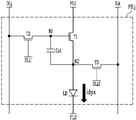
도 3을 참조하면, 화소(PXij)는 트랜지스터들(T1, T2, T3), 스토리지 커패시터(Cst), 및 발광 다이오드(LD)를 포함할 수 있다.Referring to FIG. 3 , the pixel PXij may include transistors T1 , T2 , and T3 , a storage capacitor Cst, and a light emitting diode LD.
일 실시예에서, 트랜지스터들(T1, T2, T3)은 P형 트랜지스터로 구성될 수도 있다. 다른 실시예에서, 트랜지스터들(T1, T2, T3)은 N형 트랜지스터로 구성될 수 있다. 또 다른 실시예에서, 트랜지스터들(T1, T2, T3)은 N형 트랜지스터 및 P형 트랜지스터의 조합으로 구성될 수도 있다.In one embodiment, the transistors T1 , T2 , and T3 may be configured as P-type transistors. In another embodiment, the transistors T1 , T2 , and T3 may be configured as N-type transistors. In another embodiment, the transistors T1 , T2 , and T3 may be configured as a combination of an N-type transistor and a P-type transistor.
P형 트랜지스터란 게이트 전극과 소스 전극 간의 전압 차가 음의 방향으로 증가할 때 도통되는 전류량이 증가하는 트랜지스터를 통칭한다. N형 트랜지스터란 게이트 전극과 소스 전극 간의 전압 차가 양의 방향으로 증가할 때 도통되는 전류량이 증가하는 트랜지스터를 통칭한다. 트랜지스터는 TFT(thin film transistor), FET(field effect transistor), BJT(bipolar junction transistor) 등 다양한 형태로 구성될 수 있다.The P-type transistor refers to a transistor in which an amount of conducting current increases when the voltage difference between the gate electrode and the source electrode increases in the negative direction. The N-type transistor refers to a transistor in which an amount of conducting current increases when a voltage difference between a gate electrode and a source electrode increases in a positive direction. The transistor may be configured in various forms, such as a thin film transistor (TFT), a field effect transistor (FET), or a bipolar junction transistor (BJT).
이하에서는 설명의 편의성을 위하여 트랜지스터들(T1, T2, T3)은 N형 트랜지스터로 도시한다.Hereinafter, for convenience of description, the transistors T1 , T2 , and T3 are illustrated as N-type transistors.
제1 트랜지스터(T1)는 데이터 전압(또는 데이터 신호)에 기초하여 전술한 구동 전류를 제어할 수 있다. 제1 트랜지스터(T1)의 게이트 전극이 제1 노드(N1)에 연결되고, 제1 트랜지스터(T1)의 제1 전극이 제1 전원 공급 라인(PL1)과 연결되며, 제1 트랜지스터(T1)의 제2 전극이 제2 노드(N2)에 연결될 수 있다. 제1 트랜지스터(T1)는 구동 트랜지스터(driving transistor)로 명명될 수 있다. 한편, 전원 공급 라인들 중 제1 전원 공급 라인(PL1)은 제1 전원(VDD)과 연결되고, 제1 전원(VDD)의 전압이 제1 전원 공급 라인(PL1)을 통해 제1 트랜지스터(T1)의 제1 전극에 공급될 수 있다.The first transistor T1 may control the aforementioned driving current based on the data voltage (or data signal). The gate electrode of the first transistor T1 is connected to the first node N1 , the first electrode of the first transistor T1 is connected to the first power supply line PL1 , and the A second electrode may be connected to the second node N2 . The first transistor T1 may be referred to as a driving transistor. Meanwhile, among the power supply lines, a first power supply line PL1 is connected to the first power supply VDD, and the voltage of the first power supply VDD is applied to the first transistor T1 through the first power supply line PL1 . ) may be supplied to the first electrode.
제2 트랜지스터(T2)는 제1 주사 라인(SLi1)에 턴-온 레벨의 펄스를 갖는 제1 주사 신호가 공급될 때 턴-온되어 화소(PXij)를 선택할 수 있다. 제2 트랜지스터(T2)의 게이트 전극이 제1 주사 라인(SLi1)에 연결되고, 제2 트랜지스터(T2)의 제1 전극이 데이터 라인(DLj)에 연결되고, 제2 트랜지스터(T2)의 제2 전극이 제1 노드(N1)에 연결될 수 있다. 제2 트랜지스터(T2)는 스캐닝 트랜지스터(scanning transistor)로 명명될 수 있다.The second transistor T2 is turned on when a first scan signal having a turn-on level pulse is supplied to the first scan line SLi1 to select the pixel PXij. The gate electrode of the second transistor T2 is connected to the first scan line SLi1 , the first electrode of the second transistor T2 is connected to the data line DLj, and the second electrode of the second transistor T2 is connected to the second transistor T2 . An electrode may be connected to the first node N1 . The second transistor T2 may be referred to as a scanning transistor.
제3 트랜지스터(T3)는 제2 주사 라인(SLi2)에 턴-온 레벨의 펄스를 갖는 제2 주사 신호가 공급될 때 턴-온되어 센싱 라인(ILk)에 센싱 신호들을 공급할 수 있다. 제3 트랜지스터(T3)의 게이트 전극이 제2 주사 라인(SLi2)에 연결되고, 제3 트랜지스터(T3)의 제1 전극이 제2 노드(N2)에 연결되고, 제3 트랜지스터(T3)의 제2 전극이 센싱 라인(ILk)에 연결될 수 있다. 여기서, 센싱 라인(ILk)은 초기화 전원(미도시)과 연결될 수도 있다.The third transistor T3 is turned on when a second scan signal having a turn-on level pulse is supplied to the second scan line SLi2 to supply sensing signals to the sensing line ILk. The gate electrode of the third transistor T3 is connected to the second scan line SLi2 , the first electrode of the third transistor T3 is connected to the second node N2 , and the second electrode of the third transistor T3 is connected to the second node N2 . Two electrodes may be connected to the sensing line ILk. Here, the sensing line ILk may be connected to an initialization power source (not shown).
스토리지 커패시터(Cst)는 제1 노드(N1)의 전압과 제2 노드(N2)의 전압의 전위차에 대응되는 전하량을 충전할 수 있다. 스토리지 커패시터(Cst)의 제1 전극이 제1 노드(N1)에 연결되고, 스토리지 커패시터(Cst)의 제2 전극이 제2 노드(N2)에 연결될 수 있다.The storage capacitor Cst may be charged with an amount of charge corresponding to a potential difference between the voltage of the first node N1 and the voltage of the second node N2 . A first electrode of the storage capacitor Cst may be connected to the first node N1 , and a second electrode of the storage capacitor Cst may be connected to the second node N2 .
발광 다이오드(LD)는 소정의 휘도로 발광할 수 있다. 발광 다이오드(LD)의 애노드가 제2 노드(N2)에 연결되고, 발광 다이오드(LD)의 캐소드가 제2 전원 공급 라인(PL2)에 연결될 수 있다. 한편, 전원 공급 라인들 중 제2 전원 공급 라인(PL2)은 제2 전원(VSS)과 연결되고, 제2 전원(VSS)의 전압이 제2 전원 공급 라인(PL2)을 통해 발광 다이오드(LD)의 캐소드에 공급될 수 있다.The light emitting diode LD may emit light with a predetermined luminance. The anode of the light emitting diode LD may be connected to the second node N2 , and the cathode of the light emitting diode LD may be connected to the second power supply line PL2 . Meanwhile, a second power supply line PL2 of the power supply lines is connected to the second power source VSS, and the voltage of the second power supply VSS is applied to the light emitting diode LD through the second power supply line PL2. may be supplied to the cathode of
일반적으로, 제1 전원(VDD)의 전압은 제2 전원(VSS)의 전압보다 클 수 있다. 다만, 발광 다이오드(LD)의 발광을 방지하는 등의 특수한 상황에서는 제2 전원(VSS)의 전압이 제1 전원(VDD)의 전압보다 크게 설정될 수도 있다.In general, the voltage of the first power source VDD may be greater than the voltage of the second power source VSS. However, in a special situation, such as preventing the light emitting diode LD from emitting light, the voltage of the second power source VSS may be set higher than the voltage of the first power source VDD.
표시 기간 동안, 제1 전원(VDD)의 전압은 제2 전원(VSS)의 전압보다 클 수 있다. 그리고, 데이터 라인(DLj)에는 수평 기간 단위로 순차적으로 데이터 전압들이 인가될 수 있다. 제1 주사 라인(SLi1)에는 해당하는 수평 기간에 턴-온 레벨(예, 하이 레벨)의 주사 신호가 인가될 수 있다. 그리고, 제1 주사 라인(SLi1)과 동기화되어 제2 주사 라인(SLi2)에도 턴-오프 레벨(예, 로우 레벨)의 주사 신호가 인가되거나, 표시 기간 동안 제2 주사 라인(SLi2)에 턴-오프 레벨의 주사 신호가 계속 인가될 수 있다.During the display period, the voltage of the first power source VDD may be greater than the voltage of the second power source VSS. In addition, data voltages may be sequentially applied to the data line DLj in units of horizontal periods. A scan signal of a turn-on level (eg, a high level) may be applied to the first scan line SLi1 in a corresponding horizontal period. In synchronization with the first scan line SLi1 , a scan signal of a turn-off level (eg, a low level) is also applied to the second scan line SLi2 , or a turn-off level scan signal is applied to the second scan line SLi2 during the display period. An off-level scan signal may be continuously applied.
예를 들어, 제1 주사 라인(SLi1)에 턴-온 레벨의 주사 신호가 인가되고 제2 주사 라인(SLi2)에 턴-오프 레벨의 주사 신호가 인가되면, 제2 트랜지스터(T2)는 턴-온 상태가 되고 제3 트랜지스터(T3)가 턴-오프 상태가 될 수 있다. 따라서, 화소(PXij)의 스토리지 커패시터(Cst)에는 제1 노드(N1)에 인가되는 데이터 전압 및 제2 노드(N2)의 전압 차이에 해당하는 전압이 기입된다.For example, when a scan signal of a turn-on level is applied to the first scan line SLi1 and a scan signal of a turn-off level is applied to the second scan line SLi2 , the second transistor T2 is turned-on It may be in an on state and the third transistor T3 may be in a turn-off state. Accordingly, a voltage corresponding to a voltage difference between the data voltage applied to the first node N1 and the voltage of the second node N2 is written in the storage capacitor Cst of the pixel PXij.
화소(PXij)에서, 제1 트랜지스터(T1)의 게이트 전극 및 소스 전극(예를 들어, 제1 트랜지스터(T1)의 제2 전극) 간의 전압차에 따라, 제1 전원(VDD), 제1 전원 공급 라인(PL1), 제1 트랜지스터(T1), 발광 다이오드(LD), 제2 전원 공급 라인(PL2), 및 제2 전원(VSS)을 연결하는 구동 경로로 구동 전류(idpx)가 흐르게 된다. 그리고, 구동 전류(idpx)량에 따라 발광 다이오드(LD)의 발광 휘도가 결정될 수 있다.In the pixel PXij, according to a voltage difference between the gate electrode and the source electrode of the first transistor T1 (eg, the second electrode of the first transistor T1 ), the first power source VDD and the first power source A driving current idpx flows through a driving path connecting the supply line PL1 , the first transistor T1 , the light emitting diode LD, the second power supply line PL2 , and the second power source VSS. In addition, the light emitting luminance of the light emitting diode LD may be determined according to the amount of the driving current idpx.
이후, 제1 주사 라인(SLi1) 및 제2 주사 라인(SLi2)에 턴-오프 레벨의 주사 신호가 인가되면, 제2 트랜지스터(T2) 및 제3 트랜지스터(T3)가 턴-오프 상태가 될 수 있다. 따라서, 데이터 라인(DLj)의 전압 변화에 무관하게, 스토리지 커패시터(Cst)에 의해서 제1 트랜지스터(T1)의 게이트 전극 및 소스 전극 간의 전압차가 유지되고, 발광 다이오드(LD)의 발광 휘도가 유지될 수 있다.Thereafter, when a scan signal of a turn-off level is applied to the first scan line SLi1 and the second scan line SLi2 , the second transistor T2 and the third transistor T3 may be turned off. have. Therefore, regardless of the voltage change of the data line DLj, the voltage difference between the gate electrode and the source electrode of the first transistor T1 is maintained by the storage capacitor Cst, and the light emitting luminance of the light emitting diode LD is maintained. can
화소(PXij)가 특정 블록에 포함되는 경우, 특정 블록에 포함되는 화소들 중 화소(PXij)를 제외한 나머지 화소들도 화소(PXij)와 유사하게, 표시 기간에 구동 전류들 각각이 흐르게 되어 나머지 화소들 각각에 포함된 발광 소자들도 발광함으로써 특정 블록 단위로 영상이 표시될 수 있다. 이때, 특정 블록 내에 포함된 화소들 각각에 흐르는 구동 전류들의 합이 블록 전류에 근사할 수 있다.When the pixel PXij is included in a specific block, each of the driving currents flows in the display period to the remaining pixels except for the pixel PXij among the pixels included in the specific block, similarly to the pixel PXij. The light emitting devices included in each of the light emitting devices also emit light, so that an image can be displayed in units of specific blocks. In this case, the sum of driving currents flowing through each of the pixels included in the specific block may approximate the block current.
한편, 도 4를 참조하면, 일 실시예에서, 센싱 기간 동안, 발광 다이오드(LD)의 발광을 방지하기 위해 제2 전원 공급 라인(PL2)(또는 제2 전원 공급 라인(PL2)과 연결되는 발광 다이오드(LD)의 캐소드)에 인가되는 전압이 제1 전원(VDD)의 전압보다 크게 설정될 수 있다. 한편, 다른 실시예에서, 센싱 기간 동안 제2 전원(VSS)의 전압이 제1 전원(VDD)의 전압보다 크게 설정될 수 있다. 그리고, 데이터 라인(DLj)에는 센싱 전압(미도시)이 인가될 수 있다. 그리고, 센싱 전압에 동기화되어, 제1 주사 라인(SLi1) 및 제2 주사 라인(SLi2)에 턴-온 레벨의 주사 신호들이 인가되면, 제2 트랜지스터(T2) 및 제3 트랜지스터(T3)가 턴-온될 수 있다. 여기서, 센싱 전압이 데이터 라인(DLj)에 인가되기 전에 초기화 전압(미도시)이 센싱 라인(ILk)을 통해 제2 노드(N2)에 인가될 수도 있다.Meanwhile, referring to FIG. 4 , in one embodiment, during the sensing period, the light emission connected to the second power supply line PL2 (or the second power supply line PL2 ) to prevent the light emitting diode LD from emitting light. The voltage applied to the diode LD (cathode) may be set to be greater than the voltage of the first power source VDD. Meanwhile, in another embodiment, the voltage of the second power source VSS may be set to be greater than the voltage of the first power source VDD during the sensing period. In addition, a sensing voltage (not shown) may be applied to the data line DLj. In addition, when turn-on level scan signals are applied to the first scan line SLi1 and the second scan line SLi2 in synchronization with the sensing voltage, the second transistor T2 and the third transistor T3 are turned on. - can be turned on Here, an initialization voltage (not shown) may be applied to the second node N2 through the sensing line ILk before the sensing voltage is applied to the data line DLj.
화소(PXij)의 제1 노드(N1)에 센싱 전압이 인가되어 제1 트랜지스터(T1)는 턴-온되면, 제1 전원(VDD), 제1 전원 공급 라인(PL1), 제1 트랜지스터(T1), 제2 노드(N2), 제3 트랜지스터(T3)를 연결하는 센싱 경로로, 센싱 전류(ispx)가 흐르게 된다.When the sensing voltage is applied to the first node N1 of the pixel PXij and the first transistor T1 is turned on, the first power supply VDD, the first power supply line PL1, and the first transistor T1 are turned on. ), the second node N2 , and the third transistor T3 are connected to a sensing path through which a sensing current ispx flows.
화소(PXij)가 특정 블록에 포함되는 경우, 특정 블록에 포함되는 화소들 중 화소(PXij)를 제외한 나머지 화소들도 전술한 바와 같이, 센싱 기간에 센싱 전류들 각각이 흐르게 된다. 이때, 특정 블록 내에 포함된 화소들 각각에 흐르는 센싱 전류들의 합이 블록 전류에 근사할 수 있다.When the pixel PXij is included in a specific block, each of the sensing currents flows in the sensing period in the remaining pixels except for the pixel PXij among the pixels included in the specific block as described above. In this case, the sum of sensing currents flowing through each of the pixels included in the specific block may approximate the block current.
화소(PXij)는 적색(Red), 녹색(Green) 및 청색(Blue) 중 어느 하나의 부화소이거나, 적색(Red), 녹색(Green) 및 청색(Blue)의 부화소들을 포함하는 단위 화소(또는 도트(Dot))일 수 있다. 화소(PXij)가 서로 다른 3 개의 부화소들을 포함하는 경우, 특정 패턴에서의 화소(PXij)에 포함된 부화소들의 발광 조합은 백색일 수 있다.The pixel PXij is a sub-pixel of any one of red, green, and blue, or a unit pixel including sub-pixels of red, green, and blue. or dots). When the pixel PXij includes three different sub-pixels, a light emission combination of the sub-pixels included in the pixel PXij in a specific pattern may be white.
도 3 및 도 4에 도시된 화소(PXij)는 예시적인 것이며, 본 발명의 실시예들은 다른 회로의 화소들에도 적용될 수 있다. 예를 들어, 보다 복잡한 회로를 갖는 화소들은 발광 제어 신호(emission control signal)를 더 수신하여, 발광 기간이 조절될 수도 있다.The pixel PXij shown in FIGS. 3 and 4 is exemplary, and embodiments of the present invention may be applied to pixels of other circuits. For example, pixels having a more complex circuit may further receive an emission control signal, so that the emission period may be adjusted.
이하에서는 본 발명의 일 실시예에 따른 표시 장치(1)에 포함되는 전원 인터페이스(70)의 실시예들을 구체적으로 설명하되, 이하에서는 도 4와 마찬가지로 설명의 편의성을 위해 4 개의 블록들에 대응되는 4 개의 제1 전원 공급 라인들과 4 개의 제2 전원 공급 라인들을 도시하기로 한다.Hereinafter, embodiments of the
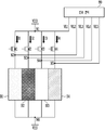
도 5는 도 1에 도시된 표시 장치에 포함된 전원 인터페이스의 일 실시예를 설명하기 위한 도면이다.FIG. 5 is a diagram for explaining an embodiment of a power interface included in the display device shown in FIG. 1 .
도 5에서는 설명의 편의성을 위해 4 개의 트랜지스터들 및 4 개의 제어 라인들을 도시하기로 한다.In FIG. 5 , four transistors and four control lines are illustrated for convenience of description.
도 5를 참조하면, 일 실시예에 따른 전원 인터페이스(70a)는 복수의 트랜지스터들(M1, M2, M3, M4)을 포함할 수 있다.Referring to FIG. 5 , the
제1 트랜지스터(M1)는 제1 블록(B1)에 제공되는 제1 블록 전류를 제어할 수 있다. 이러한 제1 트랜지스터(M1)의 제1 전극은 제1 노드(N1)에 연결되고, 제1 트랜지스터(M1)의 제2 전극은 제2 노드(N2)에 연결되며, 제1 트랜지스터(M1)의 게이트 전극은 제어 라인(CL1)과 연결될 수 있다.The first transistor M1 may control the first block current provided to the first block B1 . The first electrode of the first transistor M1 is connected to the first node N1 , the second electrode of the first transistor M1 is connected to the second node N2 , and the The gate electrode may be connected to the control line CL1 .
제2 트랜지스터(M2)는 제2 블록(B2)에 제공되는 제2 블록 전류를 제어할 수 있다. 이러한 제2 트랜지스터(M2)의 제1 전극은 제1 노드(N1)에 연결되고, 제2 트랜지스터(M2)의 제2 전극은 제3 노드(N3)에 연결되며, 제2 트랜지스터(M2)의 게이트 전극은 제어 라인(CL2)과 연결될 수 있다.The second transistor M2 may control the second block current provided to the second block B2 . The first electrode of the second transistor M2 is connected to the first node N1 , the second electrode of the second transistor M2 is connected to the third node N3 , and the The gate electrode may be connected to the control line CL2 .
제3 트랜지스터(M3)는 제3 블록(B3)에 제공되는 제3 블록 전류를 제어할 수 있다. 이러한 제3 트랜지스터(M3)의 제1 전극은 제1 노드(N1)에 연결되고, 제3 트랜지스터(M3)의 제2 전극은 제4 노드(N4)에 연결되며, 제3 트랜지스터(M3)의 게이트 전극은 제어 라인(CL3)과 연결될 수 있다.The third transistor M3 may control the third block current provided to the third block B3 . The first electrode of the third transistor M3 is connected to the first node N1 , the second electrode of the third transistor M3 is connected to the fourth node N4 , and the third transistor M3 The gate electrode may be connected to the control line CL3 .
제4 트랜지스터(M4)는 제3 블록(B3)에 제공되는 제3 블록 전류를 제어할 수 있다. 이러한 제4 트랜지스터(M4)의 제1 전극은 제1 노드(N1)에 연결되고, 제4 트랜지스터(M4)의 제2 전극은 제5 노드(N5)에 연결되며, 제4 트랜지스터(M4)의 게이트 전극은 제어 라인(CL4)과 연결될 수 있다.The fourth transistor M4 may control the third block current provided to the third block B3 . The first electrode of the fourth transistor M4 is connected to the first node N1 , the second electrode of the fourth transistor M4 is connected to the fifth node N5 , and the The gate electrode may be connected to the control line CL4 .
한편, 제1 노드(N1)에는 제1 전원(VDD)이 연결되고, 제2 노드(N2)에는 제1 전원 공급 라인(PL11)이 연결되고, 제3 노드(N3)에는 제1 전원 공급 라인(PL12)이 연결되고, 제4 노드(N4)에는 제1 전원 공급 라인(PL13)이 연결되며, 제5 노드(N5)에는 제1 전원 공급 라인(PL14)이 연결될 수 있다. 제1 전원 공급 라인들(PL11~PL14)은 전원 인터페이스(70a)의 외부에서 서로 연결될 수 있다. 예를 들어, 제1 전원 공급 라인들(PL11~PL14)은 표시부(40) 내에서 서로 연결될 수 있다.Meanwhile, the first power supply VDD is connected to the first node N1 , the first power supply line PL11 is connected to the second node N2 , and the first power supply line is connected to the third node N3 . PL12 may be connected, the first power supply line PL13 may be connected to the fourth node N4 , and the first power supply line PL14 may be connected to the fifth node N5 . The first power supply lines PL11 to PL14 may be connected to each other outside the
복수의 제2 전원 공급 라인들(PL21, PL22, PL23, PL24) 각각은 제6 노드(N6)에 연결될 수 있다. 그리고, 제6 노드(N6)에는 제2 전원(VSS)이 연결될 수 있다. 제2 전원 공급 라인들(PL21, PL22, PL23, PL24)는 전원 인터페이스(70a)의 외부에서 서로 연결될 수 있다. 예를 들어, 제2 전원 공급 라인들(PL21, PL22, PL23, PL24)은 표시부(40) 내에서 서로 연결될 수 있다. 예를 들어, 제2 전원 공급 라인들(PL21, PL22, PL23, PL24)은 표시부(40) 내의 금속 판(metal plate)에 공통적으로 연결될 수 있다.Each of the plurality of second power supply lines PL21 , PL22 , PL23 , and PL24 may be connected to the sixth node N6 . In addition, a second power source VSS may be connected to the sixth node N6 . The second power supply lines PL21 , PL22 , PL23 , and PL24 may be connected to each other outside the
도 6은 전류 센서가 블록 전류를 센싱하는 일 실시예를 설명하기 위한 도면이고, 도 7은 턴-온된 트랜지스터의 등가 저항의 저항값을 산출하는 일 실시예를 설명하기 위한 도면이다.6 is a diagram for explaining an embodiment in which a current sensor senses a block current, and FIG. 7 is a diagram for explaining an embodiment of calculating a resistance value of an equivalent resistance of a turned-on transistor.
도 6 및 도 7에서는 도 5와 마찬가지로 설명의 편의성을 위하여 4 개의 트랜지스터들 및 4 개의 제어 라인들을 도시하기로 한다.In FIGS. 6 and 7 , like FIG. 5 , four transistors and four control lines are illustrated for convenience of description.
일 실시예에 따른 전원 인터페이스(70a)는 제1 전원(VDD)과 블록 전류 제어부(90)로부터 출력되는 제어 전압에 기초하여 블록 전류들(I1, I2, I3, I4)을 제1 전원 공급 라인들(PL11, PL12, PL13, PL14) 각각에 출력할 수 있다.The
여기서, 블록 전류는 전원 인터페이스(70a)에 포함된 트랜지스터를 통해 흐르는 전류를 의미할 수 있다. 예를 들면, 제1 블록 전류(I1)는 턴-온된 제1 트랜지스터(M1)를 통해 흐르는 전류이고, 제2 블록 전류(I2)는 턴-온된 제2 트랜지스터(M2)를 통해 흐르는 전류이고, 제3 블록 전류(I3)는 턴-온된 제3 트랜지스터(M3)를 통해 흐르는 전류이며, 제4 블록 전류(I4)는 턴-온된 제4 트랜지스터(M4)를 통해 흐르는 전류일 수 있다.Here, the block current may mean a current flowing through a transistor included in the
도 5 및 도 6을 참조하여 예를 들면, 블록 전류 제어부(90)가 턴-온 레벨의 제어 전압들을 제어 라인들(CL1, CL2, CL3, CL4) 각각에 출력하고, 턴-온 레벨의 제어 전압들이 트랜지스터들(M1, M2, M3, M4) 각각의 게이트 전극에 인가되면, 트랜지스터들(M1, M2, M3, M4)은 턴-온된다.5 and 6, for example, the block
트랜지스터들(M1, M2, M3, M4)이 턴-온되면, 도 2 및 도 3을 참조하여 전술한 바와 같이 블록 전류들(I1, I2, I3, I4)이 흐르게 된다. 이때, 블록 전류들(I1, I2, I3, I4)은 제1 전원 공급 라인들(PL11, PL12, PL13, PL14) 각각을 통해 표시부(40)에 공급된다. 그리고, 블록들(B1, B2, B3, B4) 각각에 포함된 화소(PXij)들은 요구되는 휘도로 발광하므로, 블록들(B1, B2, B3, B4)은 각자의 블록 계조값에 대응되는 계조로 영상을 표시하게 된다.When the transistors M1, M2, M3, and M4 are turned on, block currents I1, I2, I3, and I4 flow as described above with reference to FIGS. 2 and 3 . In this case, the block currents I1 , I2 , I3 , and I4 are supplied to the
여기서, 블록 계조값은 블록에 포함되는 화소들 각각의 계조값들의 대표값, 블록에 포함되는 화소들 각각의 계조값들의 합, 블록에 포함되는 화소들 각각의 계조값들의 합에 대한 평균값 중 어느 하나일 수 있다. 이하에서는 설명의 편의성을 위해 블록 계조값은 블록에 포함되는 화소들 각각의 계조값들의 합인 것으로 한다.Here, the block grayscale value is any one of a representative value of each of the grayscale values of the pixels included in the block, the sum of the respective grayscale values of the pixels included in the block, and an average value of the sum of the grayscale values of each of the pixels included in the block can be one Hereinafter, for convenience of description, the block grayscale value is assumed to be the sum of grayscale values of each of the pixels included in the block.
여기서, 블록 계조값이 크면(높으면), 블록 계조값에 따른 블록 전류의 크기도 클 수 있다. 도 4 및 도 6을 참조하여 예를 들면, 제3 블록(B3)의 제3 블록 계조값이 최고 계조(예, 화이트 계조)이고, 제1 블록(B1)의 제1 블록 계조값, 제2 블록(B2)의 제2 블록 계조값 및 제4 블록(B4)의 제4 블록 계조값이 최저 계조값(예, 블랙 계조)와 최고 계조(예, 화이트 계조) 사이의 계조값인 경우, 제3 블록(B3)에 포함된 화소(예, 제3 화소(PX3))들은 최고 계조값인 제3 블록 계조값에 대응되는 계조로 발광하고, 제1 블록(B1), 제2 블록(B2) 및 제4 블록(B4) 각각에 포함된 화소(예, 제1 화소(PX1), 제2 화소(PX2) 및 제4 화소(PX4))들은 최저 계조값(예, 블랙 계조)와 최고 계조(예, 화이트 계조) 사이의 계조로 발광하므로, 블록 전류들(I1, I2, I3, I4) 중 제3 블록(B3)의 제3 블록 전류(I3)의 크기가 가장 클 수 있다.Here, if the block grayscale value is large (high), the block current according to the block grayscale value may also be large. 4 and 6 , for example, the third block grayscale value of the third block B3 is the highest grayscale (eg, white grayscale), and the first block grayscale value and the second block grayscale value of the first block B1 When the second block gradation value of the block B2 and the fourth block gradation value of the fourth block B4 are between the lowest gradation value (eg, black gradation) and the highest gradation (eg, white gradation), the first Pixels (eg, the third pixel PX3 ) included in the third block B3 emit light with a grayscale corresponding to the third block grayscale value, which is the highest grayscale value, and the first block B1 and the second block B2 and the pixels (eg, the first pixel PX1 , the second pixel PX2 , and the fourth pixel PX4 ) included in each of the fourth blocks B4 have the lowest grayscale value (eg, the black grayscale) and the highest grayscale (eg, the black grayscale). For example, since light is emitted at a gray level between white gray levels, the third block current I3 of the third block B3 may have the largest magnitude among the block currents I1 , I2 , I3 , and I4 .
블록들(B1, B2, B3, B4) 각각에 공급된 블록 전류들(I1, I2, I3, I4)은 제2 전원 공급 라인들(PL21, PL22, PL23, PL24) 각각을 통해 제2 전원(VSS)으로 흐를 수 있다.The block currents I1, I2, I3, and I4 supplied to each of the blocks B1, B2, B3, and B4 are supplied to the second power supply ( VSS) can flow.
한편, 전류 센서(80)는 측정 라인들(VL1, VL2, VL3, VL4)을 통해 블록 전류들(I1, I2, I3, I4)을 센싱할 수 있다.Meanwhile, the
예를 들면, 전류 센서(80)는 제1 노드(N1)에 연결된 측정 라인(VL1)과 제2 노드(N2)에 연결된 측정 라인(VL2)을 통해 제1 트랜지스터(M1)의 구동에 의해 조절되는 제1 블록 전류(I1)를 센싱할 수 있다.For example, the
예를 들면, 전류 센서(80)는 제1 노드(N1)에 연결된 측정 라인(VL1)과 제3 노드(N3)에 연결된 측정 라인(VL3)을 통해 제2 트랜지스터(M2)의 구동에 의해 조절되는 제2 블록 전류(I2)를 센싱할 수 있다.For example, the
예를 들면, 전류 센서(80)는 제1 노드(N1)에 연결된 측정 라인(VL1)과 제4 노드(N4)에 연결된 측정 라인(VL4)을 통해 제3 트랜지스터(M3)의 구동에 의해 조절되는 제3 블록 전류(I3)를 센싱할 수 있다.For example, the
예를 들면, 전류 센서(80)는 제1 노드(N1)에 연결된 측정 라인(VL1)과 제5 노드(N5)에 연결된 측정 라인(VL5)을 통해 제4 트랜지스터(M4)의 구동에 의해 발생하는 제4 블록 전류(I4)를 센싱할 수 있다.For example, the
전류 센서(80)는 센싱된 블록 전류들(I1, I2, I3, I4) 각각에 대응되는 센싱값들을 출력할 수 있다. 여기서, 전류 센서(80)는 전류를 센싱하는 데 필요한 센싱 저항의 양 단자의 전위차를 측정함으로써 전류를 센싱값을 출력할 수 있다. 이때, 턴-온된 트랜지스터들(M1, M2, M3, M4)은 등가 저항으로 표현될 수 있으므로, 등가 저항에 대응되는 턴-온된 트랜지스터들(M1, M2, M3, M4)을 센싱 저항으로 대체할 수 있다는 장점이 있다. 즉, 전류 센서(80)는 턴-온된 트랜지스터(M1, M2, M3, M4 중 어느 하나)의 제1 전극 및 제2 전극 간의 전위차와 턴-온된 트랜지스터(M1, M2, M3, M4 중 어느 하나)의 등가 저항의 저항값에 기초하여 블록 전류(I1, I2, I3, I4 중 어느 하나)에 대응되는 센싱값을 출력할 수 있다. The
예를 들면, 전류 센서(80)는 턴-온된 제1 트랜지스터(M1)의 제1 전극 및 제2 전극 간의 전위차와 턴-온된 제1 트랜지스터(M1)의 등가 저항의 저항값에 기초하여 제1 블록 전류(I1)에 대응되는 제1 센싱값을 출력할 수 있다. 하지만, 이에 한정되는 것은 아니며, 제2 트랜지스터(M2), 제3 트랜지스터(M3) 및 제4 트랜지스터(M4)의 경우에도 전술한 예시와 마찬가지로 적용될 수 있다.For example, the
일 실시예에서, 센싱값은 옴의 법칙(Ohm's law)에 따라 턴-온된 트랜지스터의 제1 전극 및 제2 전극 간의 전위차와 턴-온된 트랜지스터의 등가 저항의 저항값의 비율로 산출될 수 있다.In an embodiment, the sensed value may be calculated as a ratio of the potential difference between the first electrode and the second electrode of the turned-on transistor to the resistance value of the equivalent resistance of the turned-on transistor according to Ohm's law.
전류 센서(80)가 턴-온된 트랜지스터를 센싱 저항으로 대체하여 센싱값을 산출하기 위해서, 턴-온된 트랜지스터들(M1, M2, M3, M4) 각각에 대한 등가 저항의 저항값이 필요하다.In order for the
예를 들면, 등가 저항의 저항값은 게이트 전극에 턴-온 레벨의 기준 제어 전압이 입력되어 트랜지스터가 턴-온될 때 측정되는 등가 저항의 전위차와, 미리 설정된 기준 블록 계조값에 대응되는 기준 전류에 기초하여 산출될 수 있다.For example, the resistance value of the equivalent resistance corresponds to the potential difference of the equivalent resistance measured when the transistor is turned on by inputting the reference control voltage of the turn-on level to the gate electrode, and the reference current corresponding to the preset reference block grayscale value. It can be calculated based on
구체적으로, 기준 패턴이 표시부(40)에 표시되는 경우, 기준 패턴이 표시되기 위해 블록들(B1, B2, B3, B4) 각각의 기준 블록 계조값들도 산출될 수 있고, 블록들(B1, B2, B3, B4) 각각에 포함된 화소들이 기준 블록 계조값에 대응되는 계조로 발광하기 위한 기준 전류들(It1, It2, It3, It4) 각각에 대한 기준 전류값들도 산출될 수 있다.Specifically, when the reference pattern is displayed on the
한편, 턴-온 레벨의 기준 전압들이 트랜지스터들(M1, M2, M3, M4) 각각의 게이트 전극에 제공되면 트랜지스터들(M1, M2, M3, M4)이 턴-온된다. 턴-온된 트랜지스터들(M1, M2, M3, M4) 각각에 대응되는 등가 저항들의 전위차들이 측정되면, 전위차와 기준 전류값을 이용하여 턴-온된 트랜지스터에 대한 등가 저항의 저항값이 턴-온된 트랜지스터들(M1, M2, M3, M4)마다 산출될 수 있다. 여기서, 기준 패턴은 예를 들어 표시부(40)에 포함된 모든 화소들이 최고 계조로 발광하는 풀-화이트 패턴일 수 있고, 기준 블록 계조값은 최고 계조(또는 화이트 계조)일 수 있으며, 기준 전류들(It1, It2, It3, It4)은 블록 전류들로서 블록들(B1, B2, B3, B4) 각각에 포함되는 복수의 화소들이 최고 계조(예, 화이트 계조)로 발광하기 위한 전류들의 합에 대응되는 전류를 의미할 수 있다. 그리고, 기준 전류값은 기준 전류의 디지털값을 의미할 수 있다. 하지만, 이에 한정되는 것은 아니다.Meanwhile, when the reference voltages of the turn-on level are provided to the gate electrodes of each of the transistors M1, M2, M3, and M4, the transistors M1, M2, M3, and M4 are turned on. When the potential differences of the equivalent resistors corresponding to each of the turned-on transistors M1, M2, M3, and M4 are measured, the resistance value of the equivalent resistance of the turned-on transistor is obtained by using the potential difference and the reference current value. It may be calculated for each of the fields M1, M2, M3, and M4. Here, the reference pattern may be, for example, a full-white pattern in which all pixels included in the
도 6 및 도 7을 참조하여 예를 들면, 기준 패턴이 풀-화이트 패턴인 경우, 블록들(B1, B2, B3, B4)에 포함된 모든 화소들이 최고 계조로 발광하므로, 블록들(B1, B2, B3, B4) 각각의 기준 블록 계조값들도 모두 최고 계조로 계산될 수 있다. 이때, 최고 계조인 기준 블록 계조값에 대응되는 기준 전류들(It1, It2, It3, It4)도 계산될 수 있다.6 and 7 , for example, when the reference pattern is a full-white pattern, all pixels included in the blocks B1, B2, B3, and B4 emit light with the highest gray level, so that the blocks B1, B1, Each of the reference block grayscale values B2, B3, and B4) may be calculated as the highest grayscale. In this case, reference currents It1, It2, It3, It4 corresponding to the reference block grayscale value that is the highest grayscale may also be calculated.
한편, 블록 전류 제어부(90)가 턴-온 레벨의 기준 제어 전압을 트랜지스터(예, M1)의 게이트 전극에 공급하면, 트랜지스터(예, M1)는 턴-온되며, 턴-온된 트랜지스터(예, M1)는 등가 저항(예, Rdson1)으로 나타낼 수 있다. 그리고, 풀-화이트 패턴이 표시부(40)(예, 블록들(B1, B2, B3, B4))에 표시될 때, 전류 센서(80)는 등가 저항(예, Rdson1)의 전위차(예, Vt1)를 측정할 수 있다. 그 다음, 전류 센서(80)는 옴의 법칙에 따라 블록 전류에 해당하는 기준 전류(예, It1)(또는 기준 전류값)에 대한 전위차(예, Vt1)의 비율로 등가 저항(예, Rdson1)의 저항값을 계산할 수 있다. 전술한 예시는 턴-온된 제1 트랜지스터(M1)의 제1 등가 저항(Rdson1)을 기준으로 하는 실시예지만, 이에 한정되는 것은 아니며, 다른 등가 저항들(Rdson2, Rdson3, Rdson4) 각각의 저항값들도 전술한 바와 유사하게 계산될 수 있다.On the other hand, when the block
이렇게 계산된 등가 저항들(Rdson1, Rdson2, Rdson3, Rdson4)의 저항값들은 제품 출하 전에 메모리에 기입되어 정의될 수도 있고, 제품 사용 과정에서 능동적으로 재정의될 수도 있다.The resistance values of the calculated equivalent resistors Rdson1 , Rdson2 , Rdson3 , and Rdson4 may be defined by writing to the memory before shipment of the product, or may be actively redefined in the process of using the product.
전술한 바에 의하면, 별도의 센싱 저항 없이 트랜지스터만을 이용하여 블록 전류를 센싱할 수 있는 효과가 있다.As described above, there is an effect that the block current can be sensed using only the transistor without a separate sensing resistor.
또한, 전술한 바에 의하면, 별도의 센싱 저항을 추가하지 않고도 블록 전류를 센싱함으로써 제조 비용을 감소시킬 수 있는 효과가 있다.In addition, as described above, there is an effect that the manufacturing cost can be reduced by sensing the block current without adding a separate sensing resistor.
도 8은 열화 블록을 검출하는 일 실시예를 설명하기 위한 도면이다.8 is a diagram for describing an embodiment of detecting a degraded block.
도 8에서는 도 5 내지 도 7과 마찬가지로 설명의 편의성을 위하여 4 개의 트랜지스터들을 도시하기로 한다.In FIG. 8 , like FIGS. 5 to 7 , four transistors are illustrated for convenience of explanation.
도 1, 도 5 및 도 8을 참조하면, 블록 전류 제어부(90)가 제어 라인들(CL1, CL2, CL3, CL4)에 턴-온 레벨의 제어 전압들(Vc1, Vc2, Vc3, Vc4)을 출력할 수 있다. 그리고, 트랜지스터들(M1, M2, M3, M4) 각각이 제어 전압들(Vc1, Vc2, Vc3, Vc4)에 의해 턴-온되면, 블록 구동 전류들(Id1, Id2, Id3, Id4)이 표시부(40)에 제공될 수 있다. 여기서, 도 8에 도시된 블록 구동 전류들(Id1, Id2, Id3, Id4) 각각은 블록 전류들로서 표시 기간 동안 블록들(B1, B2, B3, B4) 각각에 포함되는 복수의 화소들 각각이 요구되는 휘도로 발광하기 위한 전류들의 합에 대응되는 전류를 의미할 수 있다.1, 5 and 8 , the block
예를 들면, 블록 전류 제어부(90)가 턴-온 레벨의 제1 제어 전압(Vc1)을 제어 라인(CL1)에 출력하고, 제1 제어 전압(Vc1)이 제1 트랜지스터(M1)의 게이트 전극에 공급되면, 제1 트랜지스터(M1)는 턴-온되고, 제1 블록(B1)에 포함된 화소들의 구동 전류들의 합과 대략 대응하는 제1 블록 구동 전류(Id1)가 제1 블록(B1)에 제공될 수 있다.For example, the block
블록 구동 전류들(Id1, Id2, Id3, Id4)이 블록들(B1, B2, B3, B4)에 제공됨으로써, 블록들(B1, B2, B3, B4)을 포함하는 표시부(40)는 영상 데이터에 따른 영상을 표시할 수 있다.The block driving currents Id1, Id2, Id3, and Id4 are provided to the blocks B1, B2, B3, and B4, so that the
한편, 특정 블록(예, B3)의 블록 계조값이 다른 블록들(B1, B2, B4)의 블록 계조값들보다 크면, 특정 블록(예, B3)에 제공되는 블록 구동 전류(예, Id3)의 크기가 다른 블록들(B1, B2, B4)에 제공되는 블록 구동 전류들(Id1, Id2, Id4)의 크기보다 클 수 있다.On the other hand, if the block grayscale value of a specific block (eg, B3) is greater than the block grayscale values of other blocks (B1, B2, B4), the block driving current (eg, Id3) provided to the specific block (eg, B3) may be greater than the block driving currents Id1, Id2, and Id4 provided to the other blocks B1, B2, and B4.
이 경우, 상대적으로 큰 블록 구동 전류(예, Id3)가 특정 블록(예, B3)에 제공되면, 특정 블록(예, B3)에 대응되는 영역에서 열화가 발생할 수 있다. 이와 같이 열화가 발생할 것으로 예상되는 특정 블록을 열화 블록으로 명명할 수 있다.In this case, when a relatively large block driving current (eg, Id3) is provided to a specific block (eg, B3), deterioration may occur in an area corresponding to the specific block (eg, B3). As described above, a specific block in which deterioration is expected to occur may be referred to as a deterioration block.
열화 블록의 블록 계조값은 블록들에서 열화 블록을 제외한 나머지 블록들의 블록 계조값들보다 클 수 있다. 일 실시예로, 열화 블록에서 획득된 센싱값(예, 블록 전류)은 나머지 블록들에서 획득된 센싱값들보다 클 수 있다. 다른 실시예로, 열화 블록에서 획득된 센싱값은 미리 설정된 기준 센싱값보다 클 수 있다. 여기서, 기준 센싱값은 제품의 출하 전 실험 등에 의해 메모리에 기입될 수 있다. 하지만, 이에 한정되는 것은 아니고, 제품의 출하 이후에도 필요에 따라 갱신될 수 있다. The block grayscale value of the deteriorated block may be greater than the block grayscale values of blocks other than the deteriorated block. As an embodiment, the sensed value (eg, block current) obtained from the degraded block may be greater than the sensed values obtained from the remaining blocks. In another embodiment, the sensed value obtained from the deterioration block may be greater than a preset reference sensed value. Here, the reference sensed value may be written into the memory by an experiment or the like before shipment of the product. However, the present invention is not limited thereto, and may be updated as necessary even after the product is shipped.
특정 블록(예, B3)의 블록 계조값과 다른 블록들(B1, B2, B4)의 블록 계조값들의 차이가 클수록, 특정 블록(예, B3)에 제공되는 블록 구동 전류(예, Id3)의 크기와 다른 블록들(B1, B2, B4)에 제공되는 블록 구동 전류들(Id1, Id2, Id4)의 크기의 차이도 커질 수 있으며, 전류에 의한 열화 현상은 전류값의 제곱에 비례하므로, 특정 블록(예, B3)에서 발생하는 열화가 더욱 집중될 수 있다.The greater the difference between the block grayscale value of a specific block (eg, B3) and the block grayscale values of the other blocks (B1, B2, B4), the greater the block driving current (eg, Id3) provided to the specific block (eg, B3). The difference between the size and the size of the block driving currents Id1 , Id2 , and Id4 provided to the blocks B1 , B2 , and B4 different from each other may also be large, and the deterioration due to the current is proportional to the square of the current value, The degradation occurring in the block (eg, B3) may be more concentrated.
따라서, 이를 방지하기 위해, 트랜지스터(예, M3)의 게이트 전극에 인가되는 제어 전압(예, Vc3)을 제어함으로써 열화 블록(예, B3)에 제공되는 블록 전류(예, 블록 구동 전류(Id3))를 조절할 필요가 있다.Therefore, in order to prevent this, the block current (eg, block drive current Id3) provided to the deterioration block (eg, B3) by controlling the control voltage (eg, Vc3) applied to the gate electrode of the transistor (eg, M3) ) needs to be adjusted.
한편, 블록들(B1, B2, B3, B4)의 블록 계조값들이 모두 상대적으로 높아, 블록 구동 전류들(Id1, Id2, Id3, Id4)의 크기에 대한 차이가 상대적으로 작은 경우, 특정 블록에서 열화가 발생할 확률이 낮으므로, 블록 전류 제어부(90)는, 블록 계조값들의 합이 미리 설정된 기준 계조값 이하인 경우를 개시 조건으로 하여 열화 블록의 검출 동작을 개시할 수 있다. 여기서, 미리 설정된 기준 계조값은 제품의 출하 전 실험 등에 의해 메모리에 기입될 수 있다. 하지만, 이에 한정되는 것은 아니고, 제품의 출하 이후에도 필요에 따라 갱신될 수 있다.On the other hand, when the block grayscale values of the blocks B1, B2, B3, and B4 are all relatively high and the difference in the magnitudes of the block driving currents Id1, Id2, Id3, and Id4 is relatively small, in a specific block Since the probability of occurrence of deterioration is low, the block
예를 들면, 블록 전류 제어부(90)는 제1 블록(B1)의 제1 블록 계조값, 제2 블록(B2)의 제2 블록 계조값, 제3 블록(B3)의 제3 블록 계조값, 제4 블록(B4)의 제4 블록 계조값을 모두 더하고, 블록 계조값들의 합과 기준 계조값을 비교한다. 블록 계조값들의 합이 기준 계조값 이하이면, 블록 전류 제어부(90)는 열화 블록의 검출 동작을 개시할 수 있다.For example, the block
열화 블록의 검출 동작이 개시되면, 블록 전류 제어부(90)는 블록들(B1, B2, B3, B4)의 블록 계조값들을 비교할 수 있다. 예를 들어, 블록 전류 제어부(90)는 제1 블록(B1)의 제1 블록 계조값, 제2 블록(B2)의 제2 블록 계조값, 제3 블록(B3)의 제3 블록 계조값, 제4 블록(B4)의 제4 블록 계조값을 비교할 수 있다.When the detection operation of the degraded block is started, the block
만약, 도 8에 도시된 바와 같이, 제3 블록(B3)에 포함되는 화소들이 최고 계조로 발광하는 경우, 제3 블록(B3)의 제3 블록 계조값이 다른 블록들(B1, B2, B4)의 블록 계조값들보다 클 수 있다. 이 경우, 블록 전류 제어부(90)는 제3 블록(B3)에 대한 정보를 메모리에 기입할 수 있다.If, as shown in FIG. 8 , when pixels included in the third block B3 emit light with the highest grayscale, blocks B1, B2, and B4 having different third block grayscale values of the third block B3 ) may be greater than the block grayscale values of . In this case, the block
제3 블록(B3)에 대한 정보가 저장되면, 블록 전류 제어부(90)는 전류 센서(80)로부터 센싱된 블록 구동 전류들(Id1, Id2, Id3, Id4)에 대한 센싱값들을 입력받고 블록 구동 전류들(Id1, Id2, Id3, Id4)에 대한 센싱값들을 비교한다. 그리고, 제3 블록(B3)에 제공된 제3 블록 구동 전류(Id3)에 대한 센싱값이 다른 블록들(B1, B2, B4)에 제공되는 블록 구동 전류들(Id1, Id2, Id4)에 대한 센싱값들보다 크면, 블록 전류 제어부(90)는 제3 블록(B3)을 열화 블록으로 검출할 수 있다.When information on the third block B3 is stored, the block
도 9는 검출된 열화 블록에 공급되는 블록 전류를 조절하는 실시예들을 설명하기 위한 도면이다.9 is a view for explaining embodiments of adjusting a block current supplied to a detected deteriorated block.
도 9에서는 도 5 내지 도 8과 마찬가지로 설명의 편의성을 위하여 4 개의 트랜지스터들, 4 개의 제어 전압들을 도시하기로 한다.In FIG. 9 , like FIGS. 5 to 8 , four transistors and four control voltages are illustrated for convenience of explanation.
도 8 및 도 9를 참조하면, 열화 블록(예, 제3 블록(B3))이 검출된 경우, 블록 전류 제어부(90)는 열화 블록(예, 제3 블록(B3))에 대응되는 트랜지스터(예, 제3 트랜지스터(M3))의 게이트 전극에 인가되는 제어 전압을 변경하고, 변경된 제어 전압을 열화 블록(예, 제3 블록(B3))에 대응되는 트랜지스터(예, 제3 트랜지스터(M3))의 게이트 전극에 공급한다. 여기서, 열화 블록에 공급되는 블록 전류를 조절하는 제어 전압은 열화 블록에 대응되는 트랜지스터가 턴-오프되는 턴-오프 레벨의 전압일 수 있다. 예를 들어, 제3 제어 전압(Vc3')은 제3 트랜지스터(M3)를 턴-오프시킬 수 있는 턴-오프 레벨의 전압일 수 있다.8 and 9 , when a deterioration block (eg, the third block B3) is detected, the block
도 9에 도시된 제3 제어 전압(Vc3')이 제3 트랜지스터(M3)의 게이트 전극에 인가되면, 제3 트랜지스터(M3)는 턴-오프될 수 있고, 제3 트랜지스터(M3)에 제3 블록 전류(예, 제3 블록 구동 전류(Id3))가 흐르지 않을 수 있다.When the third control voltage Vc3 ′ illustrated in FIG. 9 is applied to the gate electrode of the third transistor M3 , the third transistor M3 may be turned off, and the third transistor M3 may A block current (eg, the third block driving current Id3) may not flow.
도시되지 않았지만, 제1 전원 공급 라인들(PL11, PL12, PL13, PL14) 및 제2 전원 공급 라인들(PL21, PL22, PL23, PL24)은 표시부(40) 내에서 서로 연결될 수 있으므로, 열화 블록과 인접한 블록들에 제공되는 블록 전류들의 일부가 표시부(40) 내에서 열화 블록에 포함된 화소들에 흐를 수 있고, 이에 따라 열화 블록에 대응되는 화소들 각각이 요구되는 휘도로 발광할 수 있다.Although not shown, the first power supply lines PL11 , PL12 , PL13 , and PL14 and the second power supply lines PL21 , PL22 , PL23 , and PL24 may be connected to each other in the
한편, 블록 전류 제어부(90)는 열화 블록(예, 제3 블록(B3))에 대응되는 트랜지스터(예, 제3 트랜지스터(M3))의 게이트 전극에 인가되는 제어 전압의 변화량에 기초하여 열화 블록(예, 제3 블록(B3))에 제공되는 블록 전류(예, 제3 블록 구동 전류(Id3))의 변화량을 결정할 수 있다. 이때, 제3 제어 전압(Vc3')은 도 9에 도시된 바와 다르게 제3 트랜지스터(M3)를 턴-온 상태를 유지시키는 턴-온 레벨의 전압이지만, 제3 제어 전압(Vc3')은 도 8에 도시된 제3 제어 전압(Vc3)보다 낮은 전압일 수 있고(제3 트랜지스터(M3)가 NMOS인 경우), 이때의 제어 전압의 변화량은 제3 제어 전압(Vc3)과 제3 제어 전압(Vc3')간의 차이값에 대응되는 변화량일 수 있다.On the other hand, the block
명확히 도시되지 않았지만, 일 실시예에서, 블록 전류 제어부(90)는 열화 블록의 블록 계조값과 나머지 블록들의 블록 계조값들 중 어느 하나의 블록 계조값의 제1 차이값에 기초하여 제어 전압의 변화량을 산출할 수 있다. 여기서, 어느 하나의 블록 계조값은, 나머지 블록들의 블록 계조값들 중 가장 작은 최소 블록 계조값일 수 있다.Although not clearly shown, in an embodiment, the block
구체적으로 예를 들면, 도 8에 도시된 블록들(B1, B2, B3, B4) 중에서 최소 블록 계조값을 갖는 블록이 제2 블록(B2)인 경우, 블록 전류 제어부(90)는 열화 블록인 제3 블록(B3)의 제3 블록 계조값과 제2 블록(B2)의 제2 블록 계조값의 제1 차이값을 계산하고, 제1 차이값을 도 8에 도시된 제3 제어 전압(Vc3)에 반영하여 제3 제어 전압(Vc3)을 보정하고, 보정된 제3 제어 전압(Vc3')을 제3 트랜지스터(M3)의 게이트 전극에 인가한다. 여기서, 제1 차이값이 클수록 보정된 제3 제어 전압(Vc3')이 작을 수 있다(제3 트랜지스터(M3)가 NMOS인 경우). Specifically, for example, when the block having the minimum block grayscale value among the blocks B1, B2, B3, and B4 shown in FIG. 8 is the second block B2, the block
보정된 제3 제어 전압(Vc3')이 제3 트랜지스터(M3)의 게이트 전극에 인가되면, 변경된 제3 블록 구동 전류가 제3 블록(B3)에 제공될 수 있다. 여기서, 보정된 제3 제어 전압(Vc3')은 도 8에 도시된 제3 제어 전압(Vc3)보다 작을 수 있다(제3 트랜지스터(M3)가 NMOS인 경우).When the corrected third control voltage Vc3 ′ is applied to the gate electrode of the third transistor M3 , the changed third block driving current may be provided to the third block B3 . Here, the corrected third control voltage Vc3' may be smaller than the third control voltage Vc3 illustrated in FIG. 8 (when the third transistor M3 is an NMOS).
명확히 도시되지 않았지만, 다른 실시예에서, 블록 전류 제어부(90)는 열화 블록의 센싱값과 나머지 블록들의 센싱값들 중 어느 하나의 센싱값의 제2 차이값에 기초하여 제어 전압의 변화량을 산출할 수 있다. 여기서, 어느 하나의 센싱값은, 나머지 블록들의 센싱값들 중 가장 작은 최소 센싱값일 수 있다. Although not clearly shown, in another embodiment, the block
구체적으로 예를 들면, 도 8에 도시된 블록들(B1, B2, B3, B4) 중에서 최소 센싱값을 갖는 블록이 제2 블록(B2)인 경우, 블록 전류 제어부(90)는 열화 블록인 제3 블록(B3)의 센싱값(예, 도 8에 도시된 제3 블록 구동 전류(Id3)에 대응되는 센싱값)과 제2 블록(B2)의 센싱값(예, 도 8에 도시된 제2 블록 구동 전류(Id2)에 대응되는 센싱값)의 제2 차이값을 계산하고, 제2 차이값을 도 8에 도시된 제3 제어 전압(Vc3)에 반영하여 제3 제어 전압(Vc3)을 보정하고, 보정된 제3 제어 전압(Vc3')을 제3 트랜지스터(M3)의 게이트 전극에 인가한다. 여기서, 제2 차이값이 클수록 보정된 제3 제어 전압(Vc3')이 작을 수 있다(제3 트랜지스터(M3)가 NMOS인 경우).Specifically, for example, when the block having the minimum sensing value among the blocks B1, B2, B3, and B4 shown in FIG. 8 is the second block B2, the block
또 다른 실시예에서, 블록 전류 제어부(90)는 열화 블록의 블록 계조값과 나머지 블록들의 블록 계조값들 중 어느 하나의 블록 계조값의 제1 차이값 및 열화 블록의 센싱값과 나머지 블록들의 센싱값들 중 어느 하나의 센싱값의 제2 차이값에 기초하여 제어 전압의 변화량을 산출할 수 있다.In another embodiment, the block
한편, 열화 블록에서 획득된 센싱값은 미리 설정된 기준 센싱값보다 클 수 있으므로, 블록 전류 제어부(90)는 전술한 열화 블록의 센싱값과 나머지 블록들의 센싱값들 중 어느 하나의 센싱값의 제2 차이값 대신에 열화 블록의 센싱값과 기준 센싱값의 제2 차이값을 이용하여 제어 전압의 변화량을 결정할 수 있다.Meanwhile, since the sensed value obtained from the deterioration block may be greater than the preset reference sensed value, the block
예를 들면, 열화 블록이 제3 블록(B3)인 경우, 열화 블록인 제3 블록(B3)의 센싱값(예, 도 8에 도시된 제3 블록 구동 전류(Id3)에 대응되는 센싱값)과 기준 센싱값의 제2 차이값을 계산하고, 제2 차이값을 도 8에 도시된 제3 제어 전압(Vc3)에 반영하여 보정된 제3 제어 전압(Vc3')을 산출하며, 보정된 제3 제어 전압(Vc3')을 제3 트랜지스터(M3)의 게이트 전극에 인가한다.For example, when the deterioration block is the third block B3, the sensed value of the third block B3 that is the deterioration block (eg, the sensed value corresponding to the third block driving current Id3 illustrated in FIG. 8 )) and a second difference value of the reference sensed value is calculated, and the corrected third control voltage Vc3' is calculated by reflecting the second difference value to the third control voltage Vc3 shown in FIG. A third control voltage Vc3' is applied to the gate electrode of the third transistor M3.
전술한 예시는 제3 블록(B3)을 기준으로 설명된 것이나, 이에 한정되는 것은 아니다. 다른 블록들(B1, B2, B4) 각각에서도 전술한 실시예가 적용될 수 있다.The above-described example has been described with reference to the third block B3, but is not limited thereto. The above-described embodiment may also be applied to each of the other blocks B1, B2, and B4.
전술한 바에 의하면, 과전류에 의한 화소들의 열화 또는 발화 현상을 방지할 수 있는 효과가 있다.As described above, there is an effect of preventing deterioration or ignition of pixels due to overcurrent.
또한, 표시부(40)에서 발생하는 열화를 최소화함으로써 표시 장치(1)의 수명을 향상시킬 수 있는 효과가 있다.In addition, there is an effect of improving the lifespan of the display device 1 by minimizing deterioration occurring in the
한편, 트랜지스터(M1, M2, M3, M4)의 등가 저항에 대한 저항값 대신 전류를 센싱하는 데 이용되는 센싱 저항이 이용될 수 있다.Meanwhile, a sensing resistor used to sense a current may be used instead of a resistance value for the equivalent resistance of the transistors M1 , M2 , M3 , and M4 .
도 10은 도 5에 도시된 전원 인터페이스에 포함되는 센싱 저항의 일 실시예를 설명하기 위한 도면이고, 도 11은 전류 센서가 블록 전류를 센싱하는 다른 실시예를 설명하기 위한 도면이다.FIG. 10 is a diagram for explaining an embodiment of a sensing resistor included in the power interface shown in FIG. 5 , and FIG. 11 is a diagram for explaining another embodiment in which a current sensor senses a block current.
도 10 및 도 11에서는 설명의 편의성을 위하여 4 개의 센싱 저항들을 도시하기로 한다. 도 10 및 도 11에서 도 5에 도시된 구성과 동일한 구성에 대해서는 동일한 도면부호를 할당함과 아울러 상세한 설명은 생략하기로 한다.In FIGS. 10 and 11 , four sensing resistors are illustrated for convenience of explanation. In FIGS. 10 and 11 , the same reference numerals are assigned to the same components as those shown in FIG. 5 , and detailed descriptions thereof will be omitted.
도 10을 참조하면, 전원 인터페이스(70a)는 복수의 센싱 저항들(R1, R2, R3, R4)을 더 포함할 수 있다.Referring to FIG. 10 , the
센싱 저항들(R1, R2, R3, R4) 각각은 블록 전류를 센싱하기 위한 저항일 수 있다. 센싱 저항들(R1, R2, R3, R4) 각각의 제1 단자는 제1 전원(VDD)과 연결될 수 있고, 센싱 저항들(R1, R2, R3, R4) 각각의 제2 단자는 트랜지스터들(M1, M2, M3, M4) 각각의 제1 전극과 연결될 수 있다.Each of the sensing resistors R1, R2, R3, and R4 may be a resistor for sensing a block current. A first terminal of each of the sensing resistors R1, R2, R3, and R4 may be connected to a first power source VDD, and a second terminal of each of the sensing resistors R1, R2, R3, and R4 is connected to the transistors ( M1, M2, M3, M4) may be connected to each of the first electrode.
예를 들면, 제1 센싱 저항(R1)의 제1 단자는 제1 노드(N1)에 연결되고, 제1 센싱 저항(R1)의 제2 단자는 제7 노드(N7)에 연결될 수 있다. 여기서, 제1 전원(VDD)이 제1 노드(N1)에 연결될 수 있고, 제1 트랜지스터(M1)의 제1 전극이 제7 노드(N7)에 연결될 수 있다.For example, the first terminal of the first sensing resistor R1 may be connected to the first node N1 , and the second terminal of the first sensing resistor R1 may be connected to the seventh node N7 . Here, the first power source VDD may be connected to the first node N1 , and the first electrode of the first transistor M1 may be connected to the seventh node N7 .
예를 들면, 제2 센싱 저항(R2)의 제1 단자는 제1 노드(N1)에 연결되고, 제2 센싱 저항(R2)의 제2 단자는 제8 노드(N8)에 연결될 수 있다. 여기서, 제1 전원(VDD)이 제1 노드(N1)에 연결될 수 있고, 제2 트랜지스터(M2)의 제1 전극이 제8 노드(N8)에 연결될 수 있다.For example, a first terminal of the second sensing resistor R2 may be connected to the first node N1 , and a second terminal of the second sensing resistor R2 may be connected to the eighth node N8 . Here, the first power source VDD may be connected to the first node N1 , and the first electrode of the second transistor M2 may be connected to the eighth node N8 .
예를 들면, 제3 센싱 저항(R3)의 제1 단자는 제1 노드(N1)에 연결되고, 제3 센싱 저항(R3)의 제2 단자는 제9 노드(N9)에 연결될 수 있다. 여기서, 제1 전원(VDD)이 제1 노드(N1)에 연결될 수 있고, 제3 트랜지스터(M3)의 제1 전극이 제9 노드(N9)에 연결될 수 있다.For example, a first terminal of the third sensing resistor R3 may be connected to the first node N1 , and a second terminal of the third sensing resistor R3 may be connected to the ninth node N9 . Here, the first power source VDD may be connected to the first node N1 , and the first electrode of the third transistor M3 may be connected to the ninth node N9 .
예를 들면, 제4 센싱 저항(R4)의 제1 단자는 제1 노드(N1)에 연결되고, 제4 센싱 저항(R4)의 제2 단자는 제10 노드(N10)에 연결될 수 있다. 여기서, 제1 전원(VDD)이 제1 노드(N1)에 연결될 수 있고, 제4 트랜지스터(M4)의 제1 전극이 제10 노드(N10)에 연결될 수 있다.For example, a first terminal of the fourth sensing resistor R4 may be connected to the first node N1 , and a second terminal of the fourth sensing resistor R4 may be connected to the tenth node N10 . Here, the first power source VDD may be connected to the first node N1 , and the first electrode of the fourth transistor M4 may be connected to the tenth node N10 .
여기서, 제1 센싱 저항(R1), 제2 센싱 저항(R2), 제3 센싱 저항(R3) 및 제4 센싱 저항(R4) 각각의 저항값은 제품 출하 전에 메모리에 기입되어 정의될 수 있고, 서로 동일한 값이거나 서로 다른 값일 수 있다.Here, the resistance value of each of the first sensing resistor R1, the second sensing resistor R2, the third sensing resistor R3, and the fourth sensing resistor R4 may be defined by being written into the memory prior to shipment of the product, They may be the same value or different values.
한편, 도 10 및 도 11을 참조하면, 센싱 저항들(R1, R2, R3, R4)이 전원 인터페이스(70a)에 포함된 경우, 측정 라인들(VL1, VL2, VL3, VL4) 각각은 센싱 저항들(R1, R2, R3, R4) 각각의 양 단자에 연결될 수 있으며, 전류 센서(80)는 센싱 저항들(R1, R2, R3, R4) 각각의 양 단자의 전위차를 측정하고, 전위차와 센싱 저항들(R1, R2, R3, R4) 각각의 저항값을 이용하여 블록 전류들(I1, I2, I3, I4)에 대응되는 센싱값을 산출할 수 있다.Meanwhile, referring to FIGS. 10 and 11 , when the sensing resistors R1 , R2 , R3 , and R4 are included in the
즉, 센싱값들은, 센싱 저항들(R1, R2, R3, R4) 각각의 제1 단자가 접속된 노드(예, 제1 노드(N1))의 전압과, 센싱 저항들(R1, R2, R3, R4) 각각의 제2 단자가 접속된 노드들(예, 제7 노드(N7), 제8 노드(N8), 제9 노드(N9), 제10 노드(N10)) 각각의 전압 간의 전위차들과, 센싱 저항들(R1, R2, R3, R4) 각각의 저항값들에 기초하여 산출될 수 있다.That is, the sensed values are the voltage of the node (eg, the first node N1 ) to which the first terminal of each of the sensing resistors R1 , R2 , R3 and R4 is connected, and the sensing resistors R1 , R2 , R3 , R4) potential differences between voltages of nodes (eg, the seventh node N7 , the eighth node N8 , the ninth node N9 , and the tenth node N10 ) to which each second terminal is connected And, the sensing resistors R1, R2, R3, and R4 may be calculated based on resistance values of each.
예를 들면, 전류 센서(80)는 제1 노드(N1)에 연결된 측정 라인(VL1)과 제7 노드(N7)에 연결된 측정 라인(VL2)을 통해 제1 센싱 저항(R1)의 전위차를 측정하고, 옴의 법칙에 따라 제1 센싱 저항(R1)의 저항값에 대한 그 전위차의 비를 연산함으로써 제1 블록 전류(I1)에 대응되는 센싱값을 산출할 수 있다.For example, the
예를 들면, 전류 센서(80)는 제1 노드(N1)에 연결된 측정 라인(VL1)과 제8 노드(N8)에 연결된 측정 라인(VL3)을 통해 제2 센싱 저항(R2)의 전위차를 측정하고, 옴의 법칙에 따라 제2 센싱 저항(R2)의 저항값에 대한 그 전위차의 비를 연산함으로써 제2 블록 전류(I2)에 대응되는 센싱값을 산출할 수 있다.For example, the
예를 들면, 전류 센서(80)는 제1 노드(N1)에 연결된 측정 라인(VL1)과 제9 노드(N9)에 연결된 측정 라인(VL4)을 통해 제3 센싱 저항(R3)의 전위차를 측정하고, 옴의 법칙에 따라 제3 센싱 저항(R3)의 저항값에 대한 그 전위차의 비를 연산함으로써 제3 블록 전류(I3)에 대응되는 센싱값을 산출할 수 있다.For example, the
예를 들면, 전류 센서(80)는 제1 노드(N1)에 연결된 측정 라인(VL1)과 제10 노드(N10)에 연결된 측정 라인(VL5)을 통해 제4 센싱 저항(R4)의 전위차를 측정하고, 옴의 법칙에 따라 제4 센싱 저항(R4)의 저항값에 대한 그 전위차의 비를 연산함으로써 제4 블록 전류(I4)에 대응되는 센싱값을 산출할 수 있다.For example, the
전술한 바에 의하면, 트랜지스터들(M1, M2, M3, M4) 각각에 대한 등가 저항의 저항값을 제품의 출하 전에 미리 메모리에 기입하지 않고, 간단한 센싱 저항을 이용하여 블록 전류들을 측정함으로써, 메모리의 사용량을 저감하고, 연산 속도를 증가시키는 효과가 있다.As described above, by measuring block currents using a simple sensing resistor without writing the resistance values of the equivalent resistors for each of the transistors M1, M2, M3, and M4 in the memory before shipment of the product, the memory There is an effect of reducing the amount of use and increasing the operation speed.
도 12는 도 1에 도시된 표시 장치에 포함된 전원 인터페이스의 다른 실시예를 설명하기 위한 도면이다.FIG. 12 is a diagram for explaining another embodiment of a power interface included in the display device shown in FIG. 1 .
도 12에서 도 5에 도시된 구성과 동일한 구성에 대해서는 동일한 도면부호를 할당함과 아울러 상세한 설명은 생략하기로 한다. 아울러, 도 12에서는 도 5와 동일하게 설명의 편의성을 위하여 4 개의 블록들과, 4 개의 트랜지스터들, 4 개의 제1 전원 공급 라인들 및 4 개의 제2 전원 공급 라인들을 도시하기로 한다.In FIG. 12 , the same reference numerals are assigned to the same components as those shown in FIG. 5 , and detailed descriptions thereof will be omitted. In addition, in FIG. 12 , four blocks, four transistors, four first power supply lines, and four second power supply lines are illustrated for convenience of explanation as in FIG. 5 .
도 12를 참조하면, 본 발명의 다른 실시예에 따른 전원 인터페이스(70b)는, 도 12에 도시된 트랜지스터들(M1, M2, M3, M4)이 배치된 위치와 도 5에 도시된 트랜지스터들(M1, M2, M3, M4)이 배치된 위치가 서로 다른 점을 제외하고, 도 5에 도시된 전원 인터페이스(70a)와 동일하게 복수의 트랜지스터들(M1, M2, M3, M4)을 포함할 수 있다. Referring to FIG. 12 , the
제1 트랜지스터(M1)의 제1 전극은 제2 전원 공급 라인(PL21)과 연결되고, 제1 트랜지스터(M1)의 제2 전극은 제6 노드(N6)에 연결되며, 제1 트랜지스터(M1)의 게이트 전극은 제어 라인(CL1)과 연결될 수 있다.The first electrode of the first transistor M1 is connected to the second power supply line PL21 , the second electrode of the first transistor M1 is connected to the sixth node N6 , and the first transistor M1 The gate electrode of , may be connected to the control line CL1 .
제2 트랜지스터(M2)의 제1 전극은 제2 전원 공급 라인(PL22)과 연결되고, 제2 트랜지스터(M2)의 제2 전극은 제6 노드(N6)에 연결되며, 제2 트랜지스터(M2)의 게이트 전극은 제어 라인(CL2)과 연결될 수 있다.The first electrode of the second transistor M2 is connected to the second power supply line PL22, the second electrode of the second transistor M2 is connected to the sixth node N6, and the second transistor M2 The gate electrode of , may be connected to the control line CL2 .
제3 트랜지스터(M3)의 제1 전극은 제2 전원 공급 라인(PL23)과 연결되고, 제3 트랜지스터(M3)의 제2 전극은 제6 노드(N6)에 연결되며, 제3 트랜지스터(M3)의 게이트 전극은 제어 라인(CL3)과 연결될 수 있다.The first electrode of the third transistor M3 is connected to the second power supply line PL23 , the second electrode of the third transistor M3 is connected to the sixth node N6 , and the third transistor M3 A gate electrode of , may be connected to the control line CL3 .
제4 트랜지스터(M4)의 제1 전극은 제2 전원 공급 라인(PL24)과 연결되고, 제4 트랜지스터(M4)의 제2 전극은 제6 노드(N6)에 연결되며, 제4 트랜지스터(M4)의 게이트 전극은 제어 라인(CL4)과 연결될 수 있다.The first electrode of the fourth transistor M4 is connected to the second power supply line PL24 , the second electrode of the fourth transistor M4 is connected to the sixth node N6 , and the fourth transistor M4 A gate electrode of , may be connected to the control line CL4 .
한편, 제11 노드(N11)에는 제2 전원 공급 라인(PL21)이 연결되고, 제12 노드(N12)에는 제2 전원 공급 라인(PL22)이 연결되고, 제13 노드(N13)에는 제2 전원 공급 라인(PL23)이 연결되며, 제14 노드(N14)에는 제2 전원 공급 라인(PL24)이 연결될 수 있다.Meanwhile, the second power supply line PL21 is connected to the eleventh node N11 , the second power supply line PL22 is connected to the twelfth node N12 , and the second power supply line PL22 is connected to the thirteenth node N13 . A supply line PL23 may be connected, and a second power supply line PL24 may be connected to the 14th node N14 .
복수의 제1 전원 공급 라인들(PL11, PL12, PL13, PL14) 각각은 제1 노드(N1)에 연결될 수 있다. 그리고, 제6 노드(N6)에는 제2 전원(VSS)이 연결될 수 있다.Each of the plurality of first power supply lines PL11 , PL12 , PL13 , and PL14 may be connected to the first node N1 . In addition, a second power source VSS may be connected to the sixth node N6 .
도 13은 도 12에 도시된 전원 인터페이스에 포함되는 센싱 저항의 일 실시예를 설명하기 위한 도면이다.13 is a diagram for explaining an embodiment of a sensing resistor included in the power interface shown in FIG. 12 .
도 13을 참조하면, 도 12에 도시된 전원 인터페이스(70b)도 도 5에 도시된 전원 인터페이스(70a)와 동일하게 복수의 센싱 저항들(R1, R2, R3, R4)을 포함할 수 있다.Referring to FIG. 13 , the
예를 들면, 제1 센싱 저항(R1)은 제1 전원 공급 라인(PL11)과 제1 전원(VDD) 사이에 배치되며, 제1 센싱 저항(R1)의 제1 단자는 제1 노드(N1)에 연결되고, 제1 센싱 저항(R1)의 제2 단자는 제2 노드(N2)에 연결될 수 있다.For example, the first sensing resistor R1 is disposed between the first power supply line PL11 and the first power VDD, and the first terminal of the first sensing resistor R1 is connected to the first node N1 . , and a second terminal of the first sensing resistor R1 may be connected to the second node N2 .
예를 들면, 제2 센싱 저항(R2)은 제1 전원 공급 라인(PL12)과 제1 전원(VDD) 사이에 배치되며, 제2 센싱 저항(R2)의 제1 단자는 제1 노드(N1)에 연결되고, 제2 센싱 저항(R2)의 제2 단자는 제3 노드(N3)에 연결될 수 있다.For example, the second sensing resistor R2 is disposed between the first power supply line PL12 and the first power VDD, and the first terminal of the second sensing resistor R2 is connected to the first node N1 . , and a second terminal of the second sensing resistor R2 may be connected to the third node N3 .
예를 들면, 제3 센싱 저항(R3)은 제1 전원 공급 라인(PL13)과 제1 전원(VDD) 사이에 배치되며, 제3 센싱 저항(R3)의 제1 단자는 제1 노드(N1)에 연결되고, 제3 센싱 저항(R3)의 제2 단자는 제4 노드(N4)에 연결될 수 있다.For example, the third sensing resistor R3 is disposed between the first power supply line PL13 and the first power VDD, and the first terminal of the third sensing resistor R3 is connected to the first node N1 . , and a second terminal of the third sensing resistor R3 may be connected to the fourth node N4 .
예를 들면, 제4 센싱 저항(R4)은 제1 전원 공급 라인(PL14)과 제1 전원(VDD) 사이에 배치되며, 제4 센싱 저항(R4)의 제1 단자는 제1 노드(N1)에 연결되고, 제4 센싱 저항(R4)의 제2 단자는 제5 노드(N5)에 연결될 수 있다. For example, the fourth sensing resistor R4 is disposed between the first power supply line PL14 and the first power VDD, and the first terminal of the fourth sensing resistor R4 is connected to the first node N1 . , and a second terminal of the fourth sensing resistor R4 may be connected to the fifth node N5 .
도 13에 도시된 센싱 저항들(R1, R2, R3, R4)에 대한 설명은 도 10을 참조하여 전술한 바와 동일하므로 생략하기로 한다. Descriptions of the sensing resistors R1, R2, R3, and R4 shown in FIG. 13 are the same as those described above with reference to FIG. 10, and thus will be omitted.
도 14는 도 1에 도시된 표시 장치에 포함된 전원 인터페이스의 또 다른 실시예를 설명하기 위한 도면이다.FIG. 14 is a diagram for explaining another embodiment of a power interface included in the display device shown in FIG. 1 .
도 14를 참조하면, 본 발명의 또 다른 실시예에 따른 전원 인터페이스(70c)는 도 10에 도시된 전원 인터페이스(70a)와 유사한 구조를 갖되, 트랜지스터들(M5, M6, M7, M8)을 더 포함할 수 있다.Referring to FIG. 14 , a
제5 트랜지스터(M5)의 제1 전극은 제11 노드(N11)에 연결되고, 제5 트랜지스터(M5)의 제2 전극은 제6 노드(N6)에 연결되며, 제5 트랜지스터(M5)의 게이트 전극은 제어 라인(CL5)과 연결될 수 있다.The first electrode of the fifth transistor M5 is connected to the eleventh node N11 , the second electrode of the fifth transistor M5 is connected to the sixth node N6 , and the gate of the fifth transistor M5 is connected to the second electrode of the fifth transistor M5 . The electrode may be connected to the control line CL5 .
제6 트랜지스터(M6)의 제1 전극은 제12 노드(N12)에 연결되고, 제6 트랜지스터(M6)의 제2 전극은 제6 노드(N6)에 연결되며, 제6 트랜지스터(M6)의 게이트 전극은 제어 라인(CL6)과 연결될 수 있다.The first electrode of the sixth transistor M6 is connected to the twelfth node N12 , the second electrode of the sixth transistor M6 is connected to the sixth node N6 , and the gate of the sixth transistor M6 The electrode may be connected to the control line CL6 .
제7 트랜지스터(M7)의 제1 전극은 제13 노드(N13)에 연결되고, 제7 트랜지스터(M7)의 제2 전극은 제6 노드(N6)에 연결되며, 제7 트랜지스터(M7)의 게이트 전극은 제어 라인(CL7)과 연결될 수 있다.The first electrode of the seventh transistor M7 is connected to the thirteenth node N13 , the second electrode of the seventh transistor M7 is connected to the sixth node N6 , and the gate of the seventh transistor M7 . The electrode may be connected to the control line CL7 .
제8 트랜지스터(M8)의 제1 전극은 제14 노드(N14)에 연결되고, 제8 트랜지스터(M8)의 제2 전극은 제6 노드(N6)에 연결되며, 제8 트랜지스터(M8)의 게이트 전극은 제어 라인(CL8)과 연결될 수 있다.The first electrode of the eighth transistor M8 is connected to the fourteenth node N14 , the second electrode of the eighth transistor M8 is connected to the sixth node N6 , and the gate of the eighth transistor M8 The electrode may be connected to the control line CL8.
한편, 도 13에 도시된 바와 같이, 제11 노드(N11)에는 제2 전원 공급 라인(PL21)이 연결되고, 제12 노드(N12)에는 제2 전원 공급 라인(PL22)이 연결되고, 제13 노드(N13)에는 제2 전원 공급 라인(PL23)이 연결되며, 제14 노드(N14)에는 제2 전원 공급 라인(PL24)이 연결될 수 있다. Meanwhile, as shown in FIG. 13 , the second power supply line PL21 is connected to the eleventh node N11, the second power supply line PL22 is connected to the twelfth node N12, and the thirteenth node N11 is connected to the second power supply line PL21. A second power supply line PL23 may be connected to the node N13 , and a second power supply line PL24 may be connected to the 14th node N14 .
트랜지스터들(M5, M6, M7, M8)은 표시 기간에 턴-온되고, 센싱 기간에 턴-오프될 수 있다. 일 실시예로, 트랜지스터들(M5, M6, M7, M8) 각각은 블록 전류 제어부(90)에 의해 제어될 수 있고, 다른 실시예로, 블록 전류 제어부(90)와 타이밍 제어부(10)가 통합된 구성에 의해 제어될 수도 있다. 이러한 트랜지스터들(M5, M6, M7, M8) 각각은 센싱 트랜지스터로 명명될 수 있다. 이하에서는 센싱 트렌지스터인 트랜지스터들(M5, M6, M7, M8)가 센싱 기간에서 구동하는 실시예를 설명한다.The transistors M5, M6, M7, and M8 may be turned on during the display period and turned off during the sensing period. In one embodiment, each of the transistors M5 , M6 , M7 , and M8 may be controlled by the block
도 15는 도 14에 도시된 전원 인터페이스가 센싱 기간에 구동하는 일 실시예를 설명하기 위한 도면이다.15 is a diagram for explaining an embodiment in which the power interface shown in FIG. 14 is driven during a sensing period.
도 15를 참조하면, 센싱 트랜지스터들인 트랜지스터들(M5, M6, M7, M8)은, 센싱 기간에, 턴-오프 레벨의 제어 신호들을 제어 라인들을 통해 입력받아, 턴-오프될 수 있다.Referring to FIG. 15 , the sensing transistors M5 , M6 , M7 , and M8 may be turned off by receiving turn-off level control signals through control lines during a sensing period.
이 경우, 도시되지 않았지만, 도 4를 참조하여 전술한 바와 같이, 화소(PXij)들 각각에 포함된 발광 다이오드(LD)가 발광하는 것을 방지하기 위해, 제2 전원 공급 라인들(예, 도 13에 도시된 PL21, PL22, PL23, PL24)에 인가되는 전압은 제1 전원(VDD)의 전압보다 높을 수 있다.In this case, although not shown, as described above with reference to FIG. 4 , in order to prevent the light emitting diode LD included in each of the pixels PXij from emitting light, second power supply lines (eg, FIG. 13 ) The voltages applied to the PL21 , PL22 , PL23 , and PL24 shown in FIG. 1 may be higher than the voltage of the first power source VDD.
도 15를 참조하여 예를 들면, 도 13에 도시된 제2 전원 공급 라인(PL21)과 제5 트랜지스터(M5)의 제1 전극이 접속된 제11 노드(N11)에 인가되는 전압이 제1 전원(VDD)의 전압보다 높을 수 있다.Referring to FIG. 15 , for example, the voltage applied to the eleventh node N11 connected to the second power supply line PL21 and the first electrode of the fifth transistor M5 shown in FIG. 13 is the first power supply. It may be higher than the voltage of (VDD).
도 15를 참조하여 예를 들면, 도 13에 도시된 제2 전원 공급 라인(PL22)과 제6 트랜지스터(M6)의 제1 전극이 접속된 제12 노드(N12)에 인가되는 전압이 제1 전원(VDD)의 전압보다 높을 수 있다.Referring to FIG. 15 , for example, the voltage applied to the twelfth node N12 connected to the second power supply line PL22 and the first electrode of the sixth transistor M6 shown in FIG. 13 is the first power supply. It may be higher than the voltage of (VDD).
도 15를 참조하여 예를 들면, 도 13에 도시된 제2 전원 공급 라인(PL23)과 제7 트랜지스터(M7)의 제1 전극이 접속된 제13 노드(N13)에 인가되는 전압이 제1 전원(VDD)의 전압보다 높을 수 있다.Referring to FIG. 15 , for example, the voltage applied to the thirteenth node N13 to which the second power supply line PL23 and the first electrode of the seventh transistor M7 shown in FIG. 13 are connected is the first power source. It may be higher than the voltage of (VDD).
도 15를 참조하여 예를 들면, 도 13에 도시된 제2 전원 공급 라인(PL24)과 제8 트랜지스터(M8)의 제1 전극이 접속된 제14 노드(N14)에 인가되는 전압이 제1 전원(VDD)의 전압보다 높을 수 있다.Referring to FIG. 15 , for example, the voltage applied to the 14th node N14 to which the second power supply line PL24 and the first electrode of the eighth transistor M8 are connected is the first power supply. It may be higher than the voltage of (VDD).
트랜지스터들(M5, M6, M7, M8)이 턴-오프되면, 센싱 전류들(Is1, Is2, Is3, Is4)이 제2 전원(VSS)으로 흐르지 않고, 센싱부(50)에 제공될 수 있다. 따라서, 보상부(60)는 보상값을 산출할 수 있다.When the transistors M5 , M6 , M7 , and M8 are turned off, the sensing currents Is1 , Is2 , Is3 , and Is4 do not flow to the second power source VSS and may be provided to the
이상 첨부된 도면을 참조하여 본 발명의 실시예들을 설명하였지만, 본 발명이 속하는 기술분야에서 통상의 지식을 가진 자는 본 발명의 그 기술적 사상이나 필수적인 특징을 변경하지 않고서 다른 구체적인 형태로 실시될 수 있다는 것을 이해할 수 있을 것이다. 그러므로 이상에서 기술일 실시예들은 모든 면에서 예시적인 것이며 한정적이 아닌 것으로 이해해야만 한다.Although the embodiments of the present invention have been described above with reference to the accompanying drawings, those of ordinary skill in the art to which the present invention pertains may be embodied in other specific forms without changing the technical spirit or essential features of the present invention. you will be able to understand Therefore, it should be understood that the embodiments described above are illustrative in all respects and not restrictive.
1: 표시 장치
10: 타이밍 제어부
20: 주사 구동부
30: 데이터 구동부
40: 표시부
50: 센싱부
60: 보상부
70: 전원 인터페이스
80: 전류 센서
90: 블록 전류 제어부
B: 블록
PX: 화소
SL1: 제1 주사 라인
SL2: 제2 주사 라인
M: 트랜지스터
PL1: 제1 전원 공급 라인
PL2: 제2 전원 공급 라인
Vc: 제어 전압
VDD: 제1 전원
VSS: 제2 전원1: display device 10: timing controller
20: scan driver 30: data driver
40: display unit 50: sensing unit
60: compensation unit 70: power interface
80: current sensor 90: block current control unit
B: Block PX: Pixel
SL1: first scan line SL2: second scan line
M: Transistor PL1: First power supply line
PL2: second power supply line Vc: control voltage
VDD: first power supply VSS: second power supply
Claims (22)
제1 전원의 전압 및 제어 전압에 기초하여 상기 블록들 각각에 대응되는 블록 전류들을 제1 전원 공급 라인들 각각에 출력하는 전원 인터페이스;
상기 블록 전류들을 센싱하여 센싱값들을 출력하는 전류 센서; 및
영상 데이터를 입력받아 상기 블록들 각각에 대응되는 블록 계조값들을 계산하고, 상기 블록 계조값들 및 상기 센싱값들에 기초하여 열화 블록을 검출하고, 상기 열화 블록에 공급되는 블록 전류를 제어하기 위한 상기 제어 전압을 제어 라인에 출력하는 블록 전류 제어부를 포함하되,
상기 전원 인터페이스는,
상기 제1 전원과 연결되는 제1 전극과 상기 제1 전원 공급 라인과 연결되는 제2 전극 및 상기 제어 라인과 연결되는 게이트 전극을 포함하는 트랜지스터를 복수개 포함하는 것을 특징으로 하는 표시 장치.a display unit including pixels divided into a plurality of blocks;
a power interface for outputting block currents corresponding to each of the blocks to each of the first power supply lines based on the voltage of the first power and the control voltage;
a current sensor sensing the block currents and outputting sensed values; and
receiving image data, calculating block grayscale values corresponding to each of the blocks, detecting a deteriorated block based on the block grayscale values and the sensed values, and controlling a block current supplied to the deteriorated block; a block current control unit for outputting the control voltage to a control line;
The power interface is
and a plurality of transistors including a first electrode connected to the first power supply, a second electrode connected to the first power supply line, and a gate electrode connected to the control line.
상기 센싱값은,
턴-온된 트랜지스터의 상기 제1 전극 및 상기 제2 전극 간의 전위차와 상기 턴-온된 트랜지스터의 등가 저항의 저항값에 기초하여 산출되는 것을 특징으로 하는 표시 장치.According to claim 1,
The sensed value is
The display device is calculated based on a potential difference between the first electrode and the second electrode of the turned-on transistor and a resistance value of an equivalent resistance of the turned-on transistor.
상기 저항값은,
턴-온 레벨의 기준 제어 전압에 의해 상기 트랜지스터가 턴-온되면, 상기 턴-온된 트랜지스터의 상기 등가 저항의 전위차와, 미리 설정된 기준 블록 계조값에 대응되는 블록 전류에 기초하여 산출되는 것을 특징으로 하는 표시 장치.3. The method of claim 2,
The resistance value is
When the transistor is turned on by the reference control voltage of the turn-on level, it is calculated based on a potential difference of the equivalent resistance of the turned-on transistor and a block current corresponding to a preset reference block grayscale value. display device.
상기 열화 블록의 블록 계조값은,
상기 블록들에서 상기 열화 블록을 제외한 나머지 블록들의 블록 계조값들보다 크고,
상기 열화 블록에서 획득된 센싱값은,
상기 나머지 블록들에서 획득된 센싱값들보다 큰 것을 특징으로 하는 표시 장치.According to claim 1,
The block gradation value of the deteriorated block is,
greater than block grayscale values of blocks other than the deteriorated block in the blocks;
The sensed value obtained from the deterioration block is,
The display device of claim 1, wherein the values are greater than the sensing values obtained from the remaining blocks.
상기 열화 블록에 제공되는 상기 블록 전류의 변화량은,
상기 열화 블록에 대응되는 트랜지스터의 게이트 전극에 인가되는 제어 전압의 변화량에 기초하여 결정되고,
상기 제어 전압의 변화량은,
상기 열화 블록의 상기 블록 계조값과 상기 나머지 블록들의 상기 블록 계조값들 중 어느 하나의 블록 계조값의 제1 차이값 및 상기 열화 블록의 상기 센싱값과 상기 나머지 블록들의 상기 센싱값들 중 어느 하나의 센싱값의 제2 차이값 중 적어도 하나에 기초하여 산출되는 것을 특징으로 하는 표시 장치.5. The method of claim 4,
The change amount of the block current provided to the deterioration block is,
is determined based on a change amount of a control voltage applied to a gate electrode of a transistor corresponding to the deterioration block;
The amount of change in the control voltage is
A first difference value between the block gray value of the degraded block and any one of the block gray values of the remaining blocks, and any one of the sensed value of the degraded block and the sensed values of the remaining blocks The display device is calculated based on at least one of the second difference values of the sensed values of .
상기 어느 하나의 블록 계조값은,
상기 나머지 블록들의 상기 블록 계조값들 중 가장 작은 최소 블록 계조값이고,
어느 하나의 센싱값은,
상기 나머지 블록들의 상기 센싱값들 중 가장 작은 최소 센싱값인 것을 특징으로 하는 표시 장치.6. The method of claim 5,
Any one of the block grayscale values is
the smallest block grayscale value among the block grayscale values of the remaining blocks;
Any one of the sensing values is
The display device according to claim 1 , wherein the value is the smallest minimum sensed value among the sensed values of the remaining blocks.
상기 열화 블록의 블록 계조값은,
상기 블록들에서 상기 열화 블록을 제외한 나머지 블록들의 블록 계조값들보다 크고,
상기 열화 블록에서 획득된 센싱값은,
미리 설정된 기준 센싱값보다 큰 것을 특징으로 하는 표시 장치.According to claim 1,
The block gradation value of the deteriorated block is,
greater than block grayscale values of blocks other than the deteriorated block in the blocks;
The sensed value obtained from the deterioration block is,
A display device, characterized in that it is greater than a preset reference sensing value.
상기 열화 블록에 제공되는 상기 블록 전류의 변화량은,
상기 열화 블록에 대응되는 트랜지스터의 게이트 전극에 인가되는 제어 전압의 변화량에 기초하여 결정되고,
상기 제어 전압의 변화량은,
상기 열화 블록의 상기 블록 계조값과 상기 나머지 블록들의 상기 블록 계조값들 중 어느 하나의 블록 계조값의 제1 차이값 및 상기 열화 블록의 상기 센싱값과 상기 기준 센싱값의 제2 차이값 중 적어도 하나에 기초하여 산출되는 것을 특징으로 하는 표시 장치.8. The method of claim 7,
The change amount of the block current provided to the deterioration block is,
is determined based on a change amount of a control voltage applied to a gate electrode of a transistor corresponding to the deterioration block;
The amount of change in the control voltage is
At least one of a first difference value between the block grayscale value of the degraded block and any one of the block grayscale values of the remaining blocks and a second difference value between the sensed value of the degraded block and the reference sensed value A display device, characterized in that it is calculated based on one.
상기 블록 전류 제어부는,
상기 블록 계조값들의 합이 미리 설정된 기준 계조값 이하인 경우를 개시 조건으로 하여 상기 열화 블록의 검출 동작을 개시하는 것을 특징으로 하는 표시 장치.According to claim 1,
The block current control unit,
and starting the detecting operation of the deteriorated block under the condition that the sum of the block grayscale values is equal to or less than a preset reference grayscale value.
상기 블록 계조값은,
블록에 포함되는 화소들 각각의 계조값들의 대표값, 상기 블록에 포함되는 화소들 각각의 계조값들의 합, 블록에 포함되는 화소들 각각의 계조값들의 합에 대한 평균값 중 어느 하나인 것을 특징으로 하는 표시 장치.According to claim 1,
The block gradation value is
It is characterized in that it is any one of a representative value of each of the grayscale values of the pixels included in the block, the sum of the respective grayscale values of the pixels included in the block, and an average value of the sum of the grayscale values of each of the pixels included in the block. display device.
상기 열화 블록에 공급되는 블록 전류를 조절하는 제어 전압은,
상기 열화 블록에 대응되는 트랜지스터가 턴-오프되는 턴-오프 레벨의 전압인 것을 특징으로 하는 표시 장치.According to claim 1,
The control voltage for regulating the block current supplied to the deterioration block is,
The display device of claim 1 , wherein the voltage is at a turn-off level at which a transistor corresponding to the deterioration block is turned off.
상기 전원 인터페이스는,
상기 제1 전원에 접속되는 제1 단자와, 상기 트랜지스터의 상기 제1 전극에 접속되는 제2 단자를 구비하는 센싱 저항을 복수개 더 포함하는 것을 특징으로 하는 표시 장치.According to claim 1,
The power interface is
and a plurality of sensing resistors having a first terminal connected to the first power source and a second terminal connected to the first electrode of the transistor.
상기 센싱값들은,
상기 제1 전원과 상기 제1 단자가 접속된 노드의 전압과 상기 제1 전극과 상기 제2 단자가 접속된 노드의 전압 간의 전위차와, 상기 센싱 저항의 저항값에 기초하여 산출되는 것을 특징으로 하는 표시 장치.13. The method of claim 12,
The sensed values are
It is characterized in that calculated based on a potential difference between a voltage of a node connected to the first power supply and the first terminal and a voltage of a node connected to the first electrode and the second terminal, and a resistance value of the sensing resistor. display device.
상기 전원 인터페이스는,
상기 제1 전원 공급 라인과 다른 제2 전원 공급 라인과 연결되는 제1 전극과, 제1 전원의 전압보다 낮은 전압을 갖는 제2 전원과 연결되는 제2 전극 및 상기 제어 라인과 연결되는 게이트 전극을 포함하는 센싱 트랜지스터를 복수개 더 포함하는 것을 특징으로 하는 표시 장치.13. The method of claim 12,
The power interface is
a first electrode connected to a second power supply line different from the first power supply line, a second electrode connected to a second power having a voltage lower than the voltage of the first power supply, and a gate electrode connected to the control line; A display device further comprising a plurality of sensing transistors including:
상기 센싱 트랜지스터는,
센싱 기간에, 턴-오프 레벨의 제어 신호를 상기 제어 라인을 통해 입력받아, 턴-오프되고,
상기 제2 전원 공급 라인과 상기 센싱 트랜지스터의 상기 제1 전극이 접속된 노드에 인가되는 전압은,
상기 제1 전원의 전압보다 높은 것을 특징으로 하는 표시 장치.15. The method of claim 14,
The sensing transistor is
In the sensing period, a turn-off level control signal is input through the control line, and is turned off,
A voltage applied to a node to which the second power supply line and the first electrode of the sensing transistor are connected is,
and a voltage higher than the voltage of the first power source.
제1 전원의 전압 및 제어 전압에 기초하여 상기 블록들 각각에 대응되는 블록 전류들을 제1 전원 공급 라인들 각각에 출력하는 전원 인터페이스;
상기 블록 전류들을 센싱하여 센싱값들을 출력하는 전류 센서; 및
영상 데이터를 입력받아 상기 블록들 각각에 대응되는 블록 계조값들을 계산하고, 상기 블록 계조값들 및 상기 센싱값들에 기초하여 열화 블록을 검출하고, 상기 열화 블록에 공급되는 블록 전류를 제어하기 위한 상기 제어 전압을 제어 라인에 출력하는 블록 전류 제어부를 포함하되,
상기 전원 인터페이스는,
제2 전원 공급 라인과 연결되는 제1 전극과 상기 제1 전원의 전압보다 낮은 전압을 갖는 제2 전원과 연결되는 제2 전극 및 상기 제어 라인과 연결되는 게이트 전극을 포함하는 트랜지스터를 복수개 포함하는 것을 특징으로 하는 표시 장치.a display unit including pixels divided into a plurality of blocks;
a power interface for outputting block currents corresponding to each of the blocks to each of the first power supply lines based on the voltage of the first power and the control voltage;
a current sensor sensing the block currents and outputting sensed values; and
receiving image data, calculating block grayscale values corresponding to each of the blocks, detecting a deteriorated block based on the block grayscale values and the sensed values, and controlling a block current supplied to the deteriorated block; a block current control unit for outputting the control voltage to a control line;
The power interface is
Comprising a plurality of transistors including a first electrode connected to a second power supply line, a second electrode connected to a second power source having a voltage lower than the voltage of the first power source, and a gate electrode connected to the control line Characterized display device.
상기 센싱값은,
턴-온된 트랜지스터의 상기 제1 전극 및 상기 제2 전극 간의 전위차와 상기 턴-온된 트랜지스터의 등가 저항의 저항값에 기초하여 산출되는 것을 특징으로 하는 표시 장치.17. The method of claim 16,
The sensed value is
The display device is calculated based on a potential difference between the first electrode and the second electrode of the turned-on transistor and a resistance value of an equivalent resistance of the turned-on transistor.
상기 저항값은,
턴-온 레벨의 기준 제어 전압에 의해 상기 트랜지스터가 턴-온되면, 상기 턴-온된 트랜지스터의 상기 등가 저항의 전위차와, 미리 설정된 기준 블록 계조값에 대응되는 기준 전류에 기초하여 산출되는 것을 특징으로 하는 표시 장치.18. The method of claim 17,
The resistance value is
When the transistor is turned on by the reference control voltage of the turn-on level, it is calculated based on a potential difference of the equivalent resistance of the turned-on transistor and a reference current corresponding to a preset reference block grayscale value. display device.
상기 열화 블록의 블록 계조값은,
상기 블록들에서 상기 열화 블록을 제외한 나머지 블록들의 블록 계조값들보다 크고,
상기 열화 블록에서 획득된 센싱값은,
상기 나머지 블록들에서 획득된 센싱값들보다 큰 것을 특징으로 하는 표시 장치.17. The method of claim 16,
The block gradation value of the deteriorated block is,
greater than block grayscale values of blocks other than the deteriorated block in the blocks;
The sensed value obtained from the deterioration block is,
The display device of claim 1, wherein the values are greater than the sensing values obtained from the remaining blocks.
상기 블록 전류 제어부는,
상기 블록 계조값들의 합이 미리 설정된 기준 계조값 이하인 경우를 개시 조건으로 하여 상기 열화 블록의 검출 동작을 개시하는 것을 특징으로 하는 표시 장치.17. The method of claim 16,
The block current control unit,
and starting the detecting operation of the deteriorated block under the condition that the sum of the block grayscale values is equal to or less than a preset reference grayscale value.
상기 열화 블록에 공급되는 블록 전류를 조절하는 제어 전압은,
상기 열화 블록에 대응되는 트랜지스터가 턴-오프되는 턴-오프 레벨의 전압인 것을 특징으로 하는 표시 장치.17. The method of claim 16,
The control voltage for regulating the block current supplied to the deterioration block is,
The display device of claim 1 , wherein the voltage is at a turn-off level at which a transistor corresponding to the deterioration block is turned off.
상기 전원 인터페이스는,
상기 제1 전원에 접속되는 제1 단자와, 상기 제1 전원 공급 라인에 연결되는 제2 단자를 구비하는 센싱 저항을 복수 개 더 포함하는 것을 특징으로 하는 표시 장치.17. The method of claim 16,
The power interface is
and a plurality of sensing resistors having a first terminal connected to the first power supply and a second terminal connected to the first power supply line.
Priority Applications (3)
| Application Number | Priority Date | Filing Date | Title |
|---|---|---|---|
| KR1020200020310A KR102743340B1 (en) | 2020-02-19 | 2020-02-19 | Displya device |
| US17/028,255 US20210256892A1 (en) | 2020-02-19 | 2020-09-22 | Display device |
| CN202110185441.3A CN113362756B (en) | 2020-02-19 | 2021-02-10 | Display device |
Applications Claiming Priority (1)
| Application Number | Priority Date | Filing Date | Title |
|---|---|---|---|
| KR1020200020310A KR102743340B1 (en) | 2020-02-19 | 2020-02-19 | Displya device |
Publications (2)
| Publication Number | Publication Date |
|---|---|
| KR20210106051A true KR20210106051A (en) | 2021-08-30 |
| KR102743340B1 KR102743340B1 (en) | 2024-12-18 |
Family
ID=77271876
Family Applications (1)
| Application Number | Title | Priority Date | Filing Date |
|---|---|---|---|
| KR1020200020310A Active KR102743340B1 (en) | 2020-02-19 | 2020-02-19 | Displya device |
Country Status (3)
| Country | Link |
|---|---|
| US (1) | US20210256892A1 (en) |
| KR (1) | KR102743340B1 (en) |
| CN (1) | CN113362756B (en) |
Cited By (1)
| Publication number | Priority date | Publication date | Assignee | Title |
|---|---|---|---|---|
| WO2024154843A1 (en) * | 2023-01-18 | 2024-07-25 | 엘지전자 주식회사 | Display device and power consumption reduction method thereof |
Families Citing this family (2)
| Publication number | Priority date | Publication date | Assignee | Title |
|---|---|---|---|---|
| KR102940520B1 (en) | 2022-01-28 | 2026-03-19 | 삼성디스플레이 주식회사 | Display panel |
| KR20230172079A (en) * | 2022-06-14 | 2023-12-22 | 삼성디스플레이 주식회사 | Display device |
Citations (3)
| Publication number | Priority date | Publication date | Assignee | Title |
|---|---|---|---|---|
| KR20140039828A (en) * | 2012-09-25 | 2014-04-02 | 엘지디스플레이 주식회사 | Organic light emitting display device and driving method thereof |
| KR20140051594A (en) * | 2012-10-23 | 2014-05-02 | 엘지디스플레이 주식회사 | Display device including power control unit and method of driving the same |
| KR20150095987A (en) * | 2014-02-13 | 2015-08-24 | 삼성디스플레이 주식회사 | Burning protection circuit of a display device, display device, and method of protecting a display device from burning |
Family Cites Families (13)
| Publication number | Priority date | Publication date | Assignee | Title |
|---|---|---|---|---|
| KR100500777B1 (en) * | 2001-09-21 | 2005-07-12 | 엘지전자 주식회사 | Driving apparatus for metal-insulator-metal field emission display |
| KR100893482B1 (en) * | 2007-08-23 | 2009-04-17 | 삼성모바일디스플레이주식회사 | Organic light emitting display device and driving method thereof |
| JP2009168927A (en) * | 2008-01-11 | 2009-07-30 | Hitachi Displays Ltd | Organic EL display device |
| JP5057340B2 (en) * | 2008-03-31 | 2012-10-24 | 株式会社ジャパンディスプレイウェスト | Photodetection device, electro-optical device, and electronic apparatus |
| JP2011095720A (en) * | 2009-09-30 | 2011-05-12 | Casio Computer Co Ltd | Light-emitting apparatus, drive control method thereof, and electronic device |
| KR101809293B1 (en) * | 2010-09-06 | 2017-12-14 | 가부시키가이샤 제이올레드 | Display device and control method therefor |
| US9236011B2 (en) * | 2011-08-30 | 2016-01-12 | Lg Display Co., Ltd. | Organic light emitting diode display device for pixel current sensing in the sensing mode and pixel current sensing method thereof |
| KR101972017B1 (en) * | 2012-10-31 | 2019-04-25 | 삼성디스플레이 주식회사 | Display device, apparatus for compensating degradation and method teherof |
| KR102005052B1 (en) * | 2012-12-03 | 2019-07-31 | 삼성디스플레이 주식회사 | Error Compensation part and Organic Light Emitting Display Device Using the same |
| KR102472783B1 (en) * | 2016-02-29 | 2022-12-02 | 삼성디스플레이 주식회사 | Display device and method of compensating degradation |
| KR102505896B1 (en) * | 2016-07-29 | 2023-03-06 | 엘지디스플레이 주식회사 | Organic Light Emitting Display and Sensing Method thereof |
| KR102603596B1 (en) * | 2016-08-31 | 2023-11-21 | 엘지디스플레이 주식회사 | Organic Light Emitting Display And Degradation Sensing Method Of The Same |
| KR102653578B1 (en) * | 2016-11-25 | 2024-04-04 | 엘지디스플레이 주식회사 | Electroluminescent display device integrated with image sensor |
-
2020
- 2020-02-19 KR KR1020200020310A patent/KR102743340B1/en active Active
- 2020-09-22 US US17/028,255 patent/US20210256892A1/en not_active Abandoned
-
2021
- 2021-02-10 CN CN202110185441.3A patent/CN113362756B/en active Active
Patent Citations (3)
| Publication number | Priority date | Publication date | Assignee | Title |
|---|---|---|---|---|
| KR20140039828A (en) * | 2012-09-25 | 2014-04-02 | 엘지디스플레이 주식회사 | Organic light emitting display device and driving method thereof |
| KR20140051594A (en) * | 2012-10-23 | 2014-05-02 | 엘지디스플레이 주식회사 | Display device including power control unit and method of driving the same |
| KR20150095987A (en) * | 2014-02-13 | 2015-08-24 | 삼성디스플레이 주식회사 | Burning protection circuit of a display device, display device, and method of protecting a display device from burning |
Cited By (1)
| Publication number | Priority date | Publication date | Assignee | Title |
|---|---|---|---|---|
| WO2024154843A1 (en) * | 2023-01-18 | 2024-07-25 | 엘지전자 주식회사 | Display device and power consumption reduction method thereof |
Also Published As
| Publication number | Publication date |
|---|---|
| CN113362756B (en) | 2025-12-05 |
| CN113362756A (en) | 2021-09-07 |
| KR102743340B1 (en) | 2024-12-18 |
| US20210256892A1 (en) | 2021-08-19 |
Similar Documents
| Publication | Publication Date | Title |
|---|---|---|
| US11790833B2 (en) | Display device and an inspection method thereof | |
| KR102648976B1 (en) | Light Emitting Display Device and Driving Method thereof | |
| CN112447135B (en) | Display device driving method | |
| KR102248872B1 (en) | Organic Light Emitting Display Device | |
| CN113362756B (en) | Display device | |
| KR20150144834A (en) | Pixel circuit and organic light emitting display device having the same | |
| US20240096258A1 (en) | Display device and driving method thereof | |
| KR20210147134A (en) | Display device | |
| CN115938259A (en) | Driving method of display device | |
| CN114902319B (en) | Display device and method for driving the same | |
| KR102542142B1 (en) | Organic light emitting display device and method of manufacturing the same | |
| US11393374B2 (en) | Display device and method of driving the same | |
| CN111667787B (en) | Display device | |
| CN120690134A (en) | Voltage setting method for display device | |
| US20250174173A1 (en) | Display device and method of driving the same | |
| US12374250B2 (en) | Display device for setting margin voltage and method for operating the same | |
| US20250124849A1 (en) | System and method for setting bias voltage | |
| US12394352B2 (en) | Display device and gamma voltage setting method thereof | |
| EP4632723A1 (en) | Pixel circuit, display device including the same and electronic device including the same | |
| KR20160078639A (en) | Organic light emitting display device and organic light emitting display panel | |
| CN121640915A (en) | Display device, voltage setting method for display device, and electronic device | |
| CN117995119A (en) | Display device | |
| KR20150031639A (en) | Reference voltage generator and display device | |
| KR20200142640A (en) | Display device and driving method thereof |
Legal Events
| Date | Code | Title | Description |
|---|---|---|---|
| PA0109 | Patent application |
Patent event code: PA01091R01D Comment text: Patent Application Patent event date: 20200219 |
|
| PG1501 | Laying open of application | ||
| A201 | Request for examination | ||
| PA0201 | Request for examination |
Patent event code: PA02012R01D Patent event date: 20230202 Comment text: Request for Examination of Application Patent event code: PA02011R01I Patent event date: 20200219 Comment text: Patent Application |
|
| E902 | Notification of reason for refusal | ||
| PE0902 | Notice of grounds for rejection |
Comment text: Notification of reason for refusal Patent event date: 20240527 Patent event code: PE09021S01D |
|
| E701 | Decision to grant or registration of patent right | ||
| PE0701 | Decision of registration |
Patent event code: PE07011S01D Comment text: Decision to Grant Registration Patent event date: 20240920 |
|
| GRNT | Written decision to grant | ||
| PR0701 | Registration of establishment |
Comment text: Registration of Establishment Patent event date: 20241211 Patent event code: PR07011E01D |
|
| PR1002 | Payment of registration fee |
Payment date: 20241212 End annual number: 3 Start annual number: 1 |
|
| PG1601 | Publication of registration |