KR20200130743A - Electrostatic chuck with seal surface - Google Patents
Electrostatic chuck with seal surface Download PDFInfo
- Publication number
- KR20200130743A KR20200130743A KR1020207031813A KR20207031813A KR20200130743A KR 20200130743 A KR20200130743 A KR 20200130743A KR 1020207031813 A KR1020207031813 A KR 1020207031813A KR 20207031813 A KR20207031813 A KR 20207031813A KR 20200130743 A KR20200130743 A KR 20200130743A
- Authority
- KR
- South Korea
- Prior art keywords
- semiconductor substrate
- annular seal
- pedestal
- upper annular
- substrate
- Prior art date
- Legal status (The legal status is an assumption and is not a legal conclusion. Google has not performed a legal analysis and makes no representation as to the accuracy of the status listed.)
- Pending
Links
Images


Classifications
-
- H—ELECTRICITY
- H10—SEMICONDUCTOR DEVICES; ELECTRIC SOLID-STATE DEVICES NOT OTHERWISE PROVIDED FOR
- H10P—GENERIC PROCESSES OR APPARATUS FOR THE MANUFACTURE OR TREATMENT OF DEVICES COVERED BY CLASS H10
- H10P72/00—Handling or holding of wafers, substrates or devices during manufacture or treatment thereof
- H10P72/70—Handling or holding of wafers, substrates or devices during manufacture or treatment thereof for supporting or gripping
- H10P72/72—Handling or holding of wafers, substrates or devices during manufacture or treatment thereof for supporting or gripping using electrostatic chucks
- H10P72/722—Details of electrostatic chucks
-
- H01L21/6833—
-
- B—PERFORMING OPERATIONS; TRANSPORTING
- B23—MACHINE TOOLS; METAL-WORKING NOT OTHERWISE PROVIDED FOR
- B23Q—DETAILS, COMPONENTS, OR ACCESSORIES FOR MACHINE TOOLS, e.g. ARRANGEMENTS FOR COPYING OR CONTROLLING; MACHINE TOOLS IN GENERAL CHARACTERISED BY THE CONSTRUCTION OF PARTICULAR DETAILS OR COMPONENTS; COMBINATIONS OR ASSOCIATIONS OF METAL-WORKING MACHINES, NOT DIRECTED TO A PARTICULAR RESULT
- B23Q3/00—Devices holding, supporting, or positioning work or tools, of a kind normally removable from the machine
- B23Q3/15—Devices for holding work using magnetic or electric force acting directly on the work
-
- C—CHEMISTRY; METALLURGY
- C23—COATING METALLIC MATERIAL; COATING MATERIAL WITH METALLIC MATERIAL; CHEMICAL SURFACE TREATMENT; DIFFUSION TREATMENT OF METALLIC MATERIAL; COATING BY VACUUM EVAPORATION, BY SPUTTERING, BY ION IMPLANTATION OR BY CHEMICAL VAPOUR DEPOSITION, IN GENERAL; INHIBITING CORROSION OF METALLIC MATERIAL OR INCRUSTATION IN GENERAL
- C23C—COATING METALLIC MATERIAL; COATING MATERIAL WITH METALLIC MATERIAL; SURFACE TREATMENT OF METALLIC MATERIAL BY DIFFUSION INTO THE SURFACE, BY CHEMICAL CONVERSION OR SUBSTITUTION; COATING BY VACUUM EVAPORATION, BY SPUTTERING, BY ION IMPLANTATION OR BY CHEMICAL VAPOUR DEPOSITION, IN GENERAL
- C23C16/00—Chemical coating by decomposition of gaseous compounds, without leaving reaction products of surface material in the coating, i.e. chemical vapour deposition [CVD] processes
- C23C16/44—Chemical coating by decomposition of gaseous compounds, without leaving reaction products of surface material in the coating, i.e. chemical vapour deposition [CVD] processes characterised by the method of coating
- C23C16/458—Chemical coating by decomposition of gaseous compounds, without leaving reaction products of surface material in the coating, i.e. chemical vapour deposition [CVD] processes characterised by the method of coating characterised by the method used for supporting substrates in the reaction chamber
- C23C16/4581—Chemical coating by decomposition of gaseous compounds, without leaving reaction products of surface material in the coating, i.e. chemical vapour deposition [CVD] processes characterised by the method of coating characterised by the method used for supporting substrates in the reaction chamber characterised by material of construction or surface finish of the means for supporting the substrate
-
- H—ELECTRICITY
- H01—ELECTRIC ELEMENTS
- H01J—ELECTRIC DISCHARGE TUBES OR DISCHARGE LAMPS
- H01J37/00—Discharge tubes with provision for introducing objects or material to be exposed to the discharge, e.g. for the purpose of examination or processing thereof
- H01J37/32—Gas-filled discharge tubes
- H01J37/32009—Arrangements for generation of plasma specially adapted for examination or treatment of objects, e.g. plasma sources
- H01J37/32082—Radio frequency generated discharge
- H01J37/32091—Radio frequency generated discharge the radio frequency energy being capacitively coupled to the plasma
-
- H—ELECTRICITY
- H01—ELECTRIC ELEMENTS
- H01J—ELECTRIC DISCHARGE TUBES OR DISCHARGE LAMPS
- H01J37/00—Discharge tubes with provision for introducing objects or material to be exposed to the discharge, e.g. for the purpose of examination or processing thereof
- H01J37/32—Gas-filled discharge tubes
- H01J37/32431—Constructional details of the reactor
- H01J37/32715—Workpiece holder
-
- H01L21/67276—
-
- H01L21/6835—
-
- H—ELECTRICITY
- H02—GENERATION; CONVERSION OR DISTRIBUTION OF ELECTRIC POWER
- H02N—ELECTRIC MACHINES NOT OTHERWISE PROVIDED FOR
- H02N13/00—Clutches or holding devices using electrostatic attraction, e.g. using Johnson-Rahbek effect
-
- H—ELECTRICITY
- H10—SEMICONDUCTOR DEVICES; ELECTRIC SOLID-STATE DEVICES NOT OTHERWISE PROVIDED FOR
- H10P—GENERIC PROCESSES OR APPARATUS FOR THE MANUFACTURE OR TREATMENT OF DEVICES COVERED BY CLASS H10
- H10P72/00—Handling or holding of wafers, substrates or devices during manufacture or treatment thereof
- H10P72/06—Apparatus for monitoring, sorting, marking, testing or measuring
- H10P72/0612—Production flow monitoring, e.g. for increasing throughput
-
- H—ELECTRICITY
- H10—SEMICONDUCTOR DEVICES; ELECTRIC SOLID-STATE DEVICES NOT OTHERWISE PROVIDED FOR
- H10P—GENERIC PROCESSES OR APPARATUS FOR THE MANUFACTURE OR TREATMENT OF DEVICES COVERED BY CLASS H10
- H10P72/00—Handling or holding of wafers, substrates or devices during manufacture or treatment thereof
- H10P72/70—Handling or holding of wafers, substrates or devices during manufacture or treatment thereof for supporting or gripping
- H10P72/72—Handling or holding of wafers, substrates or devices during manufacture or treatment thereof for supporting or gripping using electrostatic chucks
-
- H—ELECTRICITY
- H10—SEMICONDUCTOR DEVICES; ELECTRIC SOLID-STATE DEVICES NOT OTHERWISE PROVIDED FOR
- H10P—GENERIC PROCESSES OR APPARATUS FOR THE MANUFACTURE OR TREATMENT OF DEVICES COVERED BY CLASS H10
- H10P72/00—Handling or holding of wafers, substrates or devices during manufacture or treatment thereof
- H10P72/70—Handling or holding of wafers, substrates or devices during manufacture or treatment thereof for supporting or gripping
- H10P72/74—Handling or holding of wafers, substrates or devices during manufacture or treatment thereof for supporting or gripping using temporarily an auxiliary support
-
- H—ELECTRICITY
- H10—SEMICONDUCTOR DEVICES; ELECTRIC SOLID-STATE DEVICES NOT OTHERWISE PROVIDED FOR
- H10P—GENERIC PROCESSES OR APPARATUS FOR THE MANUFACTURE OR TREATMENT OF DEVICES COVERED BY CLASS H10
- H10P72/00—Handling or holding of wafers, substrates or devices during manufacture or treatment thereof
- H10P72/70—Handling or holding of wafers, substrates or devices during manufacture or treatment thereof for supporting or gripping
- H10P72/76—Handling or holding of wafers, substrates or devices during manufacture or treatment thereof for supporting or gripping using mechanical means, e.g. clamps or pinches
- H10P72/7604—Handling or holding of wafers, substrates or devices during manufacture or treatment thereof for supporting or gripping using mechanical means, e.g. clamps or pinches the wafers being placed on a susceptor, stage or support
- H10P72/7611—Handling or holding of wafers, substrates or devices during manufacture or treatment thereof for supporting or gripping using mechanical means, e.g. clamps or pinches the wafers being placed on a susceptor, stage or support characterised by edge profile or support profile
-
- H—ELECTRICITY
- H10—SEMICONDUCTOR DEVICES; ELECTRIC SOLID-STATE DEVICES NOT OTHERWISE PROVIDED FOR
- H10P—GENERIC PROCESSES OR APPARATUS FOR THE MANUFACTURE OR TREATMENT OF DEVICES COVERED BY CLASS H10
- H10P72/00—Handling or holding of wafers, substrates or devices during manufacture or treatment thereof
- H10P72/70—Handling or holding of wafers, substrates or devices during manufacture or treatment thereof for supporting or gripping
- H10P72/76—Handling or holding of wafers, substrates or devices during manufacture or treatment thereof for supporting or gripping using mechanical means, e.g. clamps or pinches
- H10P72/7604—Handling or holding of wafers, substrates or devices during manufacture or treatment thereof for supporting or gripping using mechanical means, e.g. clamps or pinches the wafers being placed on a susceptor, stage or support
- H10P72/7614—Handling or holding of wafers, substrates or devices during manufacture or treatment thereof for supporting or gripping using mechanical means, e.g. clamps or pinches the wafers being placed on a susceptor, stage or support characterised by a plurality of individual support members, e.g. support posts or protrusions
-
- H—ELECTRICITY
- H01—ELECTRIC ELEMENTS
- H01J—ELECTRIC DISCHARGE TUBES OR DISCHARGE LAMPS
- H01J2237/00—Discharge tubes exposing object to beam, e.g. for analysis treatment, etching, imaging
- H01J2237/20—Positioning, supporting, modifying or maintaining the physical state of objects being observed or treated
- H01J2237/2005—Seal mechanisms
Landscapes
- Chemical & Material Sciences (AREA)
- Engineering & Computer Science (AREA)
- Physics & Mathematics (AREA)
- Plasma & Fusion (AREA)
- Analytical Chemistry (AREA)
- Mechanical Engineering (AREA)
- General Chemical & Material Sciences (AREA)
- Chemical Kinetics & Catalysis (AREA)
- Materials Engineering (AREA)
- Metallurgy (AREA)
- Organic Chemistry (AREA)
- Container, Conveyance, Adherence, Positioning, Of Wafer (AREA)
- Drying Of Semiconductors (AREA)
- Automation & Control Theory (AREA)
Abstract
페데스탈들을 위한 장치들 및 시스템들이 제공된다. 예시적인 페데스탈은 평면형이고, 바디의 수직 중심 축에 수직이고, 방사상 두께를 갖는 상부 환형 시일 표면, 상부 환형 시일 표면으로부터 오프셋된 하부 리세스 표면, 및 하부 리세스 표면으로부터 돌출하는 복수의 MCA들 (micro-contact areas) 로서, MCA 각각은 하부 리세스 표면으로부터 제 1 거리 이하인 제 2 거리만큼 오프셋된 상단 표면을 갖는, 복수의 MCA들 및 바디 내 하나 이상의 전극들을 갖는 바디를 가질 수도 있다. 상부 환형 시일 표면은 반도체 기판이 페데스탈에 의해 지지될 때 반도체 기판의 외측 에지를 지지하도록 구성될 수도 있고, 상부 환형 시일 표면 및 MCA들의 상단부들은 반도체 기판이 페데스탈에 의해 지지될 때 반도체 기판을 지지하도록 구성될 수도 있다. Devices and systems for pedestales are provided. An exemplary pedestal is planar, perpendicular to the vertical central axis of the body, and having a radial thickness of the upper annular seal surface, the lower recess surface offset from the upper annular seal surface, and a plurality of MCAs projecting from the lower recess surface ( As micro-contact areas), each MCA may have a body with a plurality of MCAs and one or more electrodes in the body, with a top surface offset by a second distance less than the first distance from the lower recess surface. The upper annular seal surface may be configured to support the outer edge of the semiconductor substrate when the semiconductor substrate is supported by the pedestal, and the upper annular seal surface and the upper ends of the MCAs support the semiconductor substrate when the semiconductor substrate is supported by the pedestal. It can also be configured.

Description
참조로서 인용Quoted by reference
PCT 신청 양식이 본 출원의 일부로서 본 명세서와 동시에 제출되었다. 본 출원이 동시에 제출된 PCT 신청 양식에서 식별된 바와 같이 우선권 또는 이익을 주장하는 출원 각각은 전체가 모든 목적들을 위해 참조로서 인용되었다.A PCT application form was filed concurrently with this specification as part of this application. Each of the applications claiming priority or benefit as identified in the PCT application form to which this application was filed at the same time is incorporated by reference in its entirety for all purposes.
반도체 프로세싱 동작들 동안, 기판이 통상적으로 프로세싱 챔버 내 페데스탈 상에 지지된다. During semiconductor processing operations, a substrate is typically supported on a pedestal in a processing chamber.
본 개시의 시스템들, 방법들 및 디바이스들은 각각 몇몇 혁신적인 양태들을 갖고, 이들이 단독으로 본 명세서에 개시된 바람직한 속성들을 유일하게 담당하지 않는다. 이들 양태들 중 적어도 이하의 구현예들이 포함되지만, 다른 구현예들이 상세한 기술에 제시될 수도 있고 본 명세서에 제공된 논의로부터 자명할 수도 있다. The systems, methods and devices of the present disclosure each have several innovative aspects, and they are not solely responsible for the desirable attributes disclosed herein. At least the following implementations of these aspects are included, but other implementations may be presented in the detailed description and may be apparent from the discussion provided herein.
일부 실시예들에서, 페데스탈이 제공될 수도 있다. 페데스탈은 평면형이고, 바디의 수직 중심 축에 수직이고, 그리고 방사상 두께를 갖는 상부 환형 시일 표면, 상부 환형 시일 표면으로부터 제 1 거리만큼 오프셋되는 하부 리세스 표면, 하부 리세스 표면으로부터 돌출하는 복수의 마이크로-콘택트 영역들 (micro-contact areas; MCAs) 로서, MCA 각각은 하부 리세스 표면으로부터 제 1 거리 이하인 제 2 거리만큼 오프셋된 상단 표면을 갖는 복수의 MCA들, 및 바디 내 하나 이상의 전극들을 포함하는 바디를 포함할 수도 있다. 상부 환형 시일 표면은 반도체 기판이 페데스탈에 의해 지지될 때 반도체 기판의 외측 에지를 지지하도록 구성될 수도 있고, 상부 환형 시일 표면 및 MCA들의 상단 표면들은 반도체 기판이 페데스탈에 의해 지지될 때 반도체 기판을 지지하도록 구성될 수도 있고, 그리고 하나 이상의 전극들은 RF (radio frequency) 전력 공급부, 전기적 접지, 및 DC (direct current) 전력 공급부와 전기적으로 접속되도록 구성될 수도 있다. In some embodiments, a pedestal may be provided. The pedestal is planar, perpendicular to the vertical central axis of the body, and having a radial thickness of the upper annular seal surface, the lower recess surface offset by a first distance from the upper annular seal surface, and a plurality of micros projecting from the lower recess surface. -As micro-contact areas (MCAs), each MCA comprising a plurality of MCAs having a top surface offset by a second distance less than or equal to a first distance from the lower recess surface, and one or more electrodes in the body. It may also include a body. The upper annular seal surface may be configured to support the outer edge of the semiconductor substrate when the semiconductor substrate is supported by the pedestal, and the upper annular seal surface and the top surfaces of the MCAs support the semiconductor substrate when the semiconductor substrate is supported by the pedestal. And the one or more electrodes may be configured to be electrically connected with a radio frequency (RF) power supply, an electrical ground, and a direct current (DC) power supply.
일부 실시예들에서, 하나 이상의 정전 클램프 전극들은 정전 클램프 전극들일 수도 있고, 하나 이상의 정전 클램프 전극들은 반도체 기판이 페데스탈에 의해 지지될 때 그리고 하나 이상의 정전 클램프 전극들이 DC 전력 공급부에 의해 전력공급될 (powered) 때 반도체 기판 상에 정전 클램핑력을 제공하도록 구성될 수도 있다. In some embodiments, the one or more electrostatic clamp electrodes may be electrostatic clamp electrodes, the one or more electrostatic clamp electrodes when the semiconductor substrate is supported by the pedestal and the one or more electrostatic clamp electrodes are powered by the DC power supply ( powered) may be configured to provide an electrostatic clamping force on the semiconductor substrate.
일부 이러한 실시예들에서, 반도체 기판이 페데스탈에 의해 지지될 때 그리고 하나 이상의 정전 클램프 전극들이 반도체 기판 상에 정전 클램핑력을 제공할 때 시일이 상부 환형 시일 표면과 반도체 기판 사이에 생성될 수도 있다. In some such embodiments, a seal may be created between the upper annular seal surface and the semiconductor substrate when the semiconductor substrate is supported by the pedestal and when one or more electrostatic clamp electrodes provide an electrostatic clamping force on the semiconductor substrate.
일부 실시예들에서, 하나 이상의 전극들은 RF 전력 공급부와 전기적으로 접속될 수도 있고, 또는 RF 전력 공급부로부터 RF 전력을 수용하도록 구성될 수도 있다.In some embodiments, one or more electrodes may be electrically connected with the RF power supply, or may be configured to receive RF power from the RF power supply.
일부 실시예들에서, 상부 환형 시일 표면은 반도체 기판의 반경보다 작은 내측 반경 및 반도체 기판의 반경보다 큰 외측 반경을 가질 수도 있다. In some embodiments, the upper annular seal surface may have an inner radius less than the radius of the semiconductor substrate and an outer radius greater than the radius of the semiconductor substrate.
일부 이러한 실시예들에서, 내측 반경은 약 142 ㎜일 수도 있다. In some such embodiments, the inner radius may be about 142 mm.
일부 다른 이러한 실시예들에서, 외측 반경은 약 150 ㎜일 수도 있다.In some other such embodiments, the outer radius may be about 150 mm.
일부 실시예들에서, 방사상 두께는 약 25 ㎜ 이하일 수도 있다.In some embodiments, the radial thickness may be about 25 mm or less.
일부 이러한 실시예들에서, 방사상 두께는 약 15 ㎜ 이하일 수도 있다.In some such embodiments, the radial thickness may be about 15 mm or less.
일부 실시예들에서, MCA들의 상부 환형 시일 표면 및 상단 표면들은 동일 평면상일 수도 있고, 제 1 거리는 제 2 거리와 같을 수도 있다.In some embodiments, the top annular seal surface and top surfaces of the MCAs may be coplanar, and the first distance may be equal to the second distance.
일부 이러한 실시예들에서, 제 1 거리 및 제 2 거리는 0.0127 ㎜와 0.0381 ㎜ 사이이거나 같을 수도 있다.In some such embodiments, the first distance and the second distance may be between or equal to 0.0127 mm and 0.0381 mm.
일부 다른 이러한 실시예들에서, 제 1 거리 및 제 2 거리는 0.0254 ㎜일 수도 있다.In some other such embodiments, the first distance and the second distance may be 0.0254 mm.
일부 실시예들에서, 제 1 거리는 제 2 거리보다 클 수도 있다. In some embodiments, the first distance may be greater than the second distance.
일부 이러한 실시예들에서, 제 1 거리 및 제 2 거리는 0.0127 ㎜와 0.0381 ㎜ 사이이거나 같을 수도 있다.In some such embodiments, the first distance and the second distance may be between or equal to 0.0127 mm and 0.0381 mm.
일부 실시예들에서, 복수의 MCA들은 2,000 개보다 많은 MCA들을 포함할 수도 있다.In some embodiments, the plurality of MCAs may include more than 2,000 MCAs.
일부 이러한 실시예들에서, 복수의 MCA들은 4,000 개보다 많은 MCA들을 포함할 수도 있다.In some such embodiments, multiple MCAs may include more than 4,000 MCAs.
일부 이러한 실시예들에서, 실질적으로 모든 MCA들은 서로 균등하게 이격될 수도 있다. In some such embodiments, substantially all of the MCAs may be evenly spaced from each other.
일부 다른 이러한 실시예들에서, 실질적으로 모든 MCA들이 3.9 ㎜만큼 서로 이격될 수도 있다.In some other such embodiments, substantially all of the MCAs may be spaced apart from each other by 3.9 mm.
일부 이러한 실시예들에서, 복수의 MCA들은 복수의 하위-배열들로 분할될 수도 있고, 하위-배열 각각의 MCA들은 하부 리세스 표면 상에 삼각형 패턴, 사각형 패턴, 대칭 패턴, 방사상 배열, 또는 육각형 패턴으로 위치될 수도 있다. In some such embodiments, a plurality of MCAs may be divided into a plurality of sub-arrays, and each of the sub-arrays of MCAs is a triangular pattern, a square pattern, a symmetric pattern, a radial arrangement, or a hexagonal shape on the lower recess surface It can also be positioned in a pattern.
일부 실시예들에서, 하부 리세스 표면은 리세스 표면적을 가질 수도 있고, MCA 상단 표면 각각은 상단 표면적을 가질 수도 있고, 복수의 MCA들의 MCA들의 총 전체 상단 표면적은 리세스 표면적의 3 % 이하일 수도 있다.In some embodiments, the lower recess surface may have a recess surface area, each of the MCA top surfaces may have a top surface area, and the total total top surface area of the MCAs of the plurality of MCAs may be 3% or less of the recess surface area. have.
일부 실시예들에서, MCA 각각은 평면형 상단 표면적을 갖는 원통형일 수도 있다.In some embodiments, each MCA may be cylindrical with a planar top surface area.
일부 이러한 실시예들에서, MCA 각각의 반경은 약 0.35 ㎜일 수도 있다.In some such embodiments, the radius of each MCA may be about 0.35 mm.
일부 실시예들에서, 상부 환형 시일 표면은 0.8128 ㎛ 내지 약 0.2032 ㎛의 거칠기를 가질 수도 있다.In some embodiments, the upper annular seal surface may have a roughness of 0.8128 μm to about 0.2032 μm.
일부 실시예들에서, MCA 각각 상단 표면은 0.8128 ㎛ 내지 약 0.2032 ㎛의 거칠기를 가질 수도 있다. In some embodiments, the top surface of each MCA may have a roughness of 0.8128 μm to about 0.2032 μm.
일부 실시예들에서, 상부 환형 시일 표면은 0.0254 ㎜의 최대 범위를 갖는 평탄도를 가질 수도 있다.In some embodiments, the upper annular seal surface may have a flatness with a maximum range of 0.0254 mm.
일부 실시예들에서, MCA 각각 상단 표면은 0.0254 ㎜의 최대 범위를 갖는 평탄도를 가질 수도 있다. In some embodiments, each top surface of the MCA may have a flatness with a maximum range of 0.0254 mm.
일부 실시예들에서, 바디는 세라믹을 포함할 수도 있다.In some embodiments, the body may comprise ceramic.
일부 실시예들에서, 바디는 금속 또는 금속 합금을 포함할 수도 있고, 그리고 바디는 세라믹으로 코팅될 수도 있다.In some embodiments, the body may comprise a metal or a metal alloy, and the body may be coated with a ceramic.
일부 실시예들에서, 반도체 프로세싱 시스템이 포함될 수도 있다. 시스템은 프로세싱 챔버, 프로세싱 챔버의 하나 이상의 프로세싱 스테이션들, 하나 이상의 프로세싱 스테이션들 각각에 정전 척을 포함할 수도 있다. 정전 척 각각은 평면형이고, 바디의 수직 중심 축에 수직이고, 그리고 방사상 두께를 갖는 상부 환형 시일 표면, 상부 환형 시일 표면으로부터 제 1 거리만큼 오프셋되는 하부 리세스 표면, 하부 리세스 표면으로부터 돌출하는 복수의 MCA들 (micro-contact areas) 로서, MCA 각각은 하부 리세스 표면으로부터 제 1 거리 이하인 제 2 거리만큼 오프셋된 상단 표면을 갖는 복수의 MCA들, 및 바디 내 하나 이상의 정전 클램프 전극들을 포함하는 바디를 포함할 수도 있다. 상부 환형 시일 표면은 반도체 기판이 정전 척에 의해 지지될 때 반도체 기판의 외측 에지를 지지하도록 구성될 수도 있고, 상부 환형 시일 표면 및 MCA들의 상단 표면들은 반도체 기판이 정전 척에 의해 지지될 때 반도체 기판을 지지하도록 구성될 수도 있고, 그리고 하나 이상의 정전 클램프 전극들은 반도체 기판이 정전 척에 의해 지지될 때 그리고 하나 이상의 정전 클램프 전극들이 DC 전력 공급부에 의해 전력공급될 때 반도체 기판 상에 정전 클램핑력을 제공하도록 구성될 수도 있다. 시스템은 또한 정전 클램프 전극들에 전기적으로 접속된 DC 전력 소스 및 메모리 및 프로세서를 갖는 제어기를 포함할 수도 있고, 메모리는 DC 전력 소스로 하여금 반도체 기판이 정전 척에 의해 지지될 때 반도체 기판 상에 정전 클램핑력을 제공하기 위해 정전 클램프 전극들에 전력을 제공하게 하도록 구성된 인스트럭션들을 저장한다.In some embodiments, a semiconductor processing system may be included. The system may include an electrostatic chuck in each of the processing chamber, one or more processing stations of the processing chamber, and one or more processing stations. Each of the electrostatic chucks is planar, perpendicular to the vertical central axis of the body, and having a radial thickness, an upper annular seal surface, a lower recess surface offset by a first distance from the upper annular seal surface, a plurality of protruding from the lower recess surface. A body comprising a plurality of MCAs having a top surface offset by a second distance less than a first distance from a lower recess surface, and one or more electrostatic clamp electrodes in the body, wherein each MCA is It may also include. The upper annular seal surface may be configured to support the outer edge of the semiconductor substrate when the semiconductor substrate is supported by the electrostatic chuck, and the upper annular seal surface and the upper surfaces of the MCAs are semiconductor substrates when the semiconductor substrate is supported by the electrostatic chuck. And the one or more electrostatic clamp electrodes provide an electrostatic clamping force on the semiconductor substrate when the semiconductor substrate is supported by the electrostatic chuck and when the one or more electrostatic clamp electrodes are powered by the DC power supply. It may be configured to do. The system may also include a controller having a DC power source and memory and processor electrically connected to the electrostatic clamp electrodes, the memory allowing the DC power source to cause an electrostatic charge on the semiconductor substrate when the semiconductor substrate is supported by the electrostatic chuck. It stores instructions configured to provide power to the electrostatic clamp electrodes to provide a clamping force.
일부 실시예들에서, 시스템은 정전 척들 각각 상에 반도체 기판을 위치시키도록 구성된 엔드 이펙터를 더 포함할 수도 있다. 메모리는 엔드 이펙터로 하여금 정전 척들 각각 상에 반도체 기판을 위치시키게 하고, 그리고 반도체 기판을 정전 척들 중 하나 상에 위치시킨 후, DC 전력 소스로 하여금 반도체 기판 상에 정전 클램핑력을 제공하기 위해 일 정전 척의 정전 클램프 전극들에 전력을 제공하게 하도록 구성된 인스트럭션들을 더 저장할 수도 있다.In some embodiments, the system may further include an end effector configured to position the semiconductor substrate on each of the electrostatic chucks. The memory causes the end effector to position the semiconductor substrate on each of the electrostatic chucks, and after placing the semiconductor substrate on one of the electrostatic chucks, the DC power source causes one electrostatic force to provide an electrostatic clamping force on the semiconductor substrate. It may further store instructions configured to provide power to the electrostatic clamp electrodes of the chuck.
일부 실시예들에서, 메모리는 엔드 이펙터가 반도체 기판을 정전 척들 중 하나 상에 위치시키는 동안, DC 전력 소스로 하여금 반도체 기판 상에 보다 낮은 정전 클램핑력을 제공하기 위해 일 정전 척의 정전 클램프 전극들에 전력을 제공하게 하도록 구성된 인스트럭션들을 더 저장할 수도 있다. In some embodiments, the memory is applied to the electrostatic clamp electrodes of one electrostatic chuck to cause the DC power source to provide a lower electrostatic clamping force on the semiconductor substrate while the end effector positions the semiconductor substrate on one of the electrostatic chuck. It may further store instructions configured to provide power.
일부 실시예들에서, 반도체 프로세싱 시스템이 포함될 수도 있다. 시스템은 프로세싱 챔버, 프로세싱 챔버의 하나 이상의 프로세싱 스테이션들, 및 하나 이상의 프로세싱 스테이션들 각각의 페데스탈을 포함할 수도 있다. 페데스탈 각각은 평면형이고, 바디의 수직 중심 축에 수직이고, 그리고 방사상 두께를 갖는 상부 환형 시일 표면, 상부 환형 시일 표면으로부터 제 1 거리만큼 오프셋되는 하부 리세스 표면, 하부 리세스 표면으로부터 돌출하는 복수의 MCA들 (micro-contact areas) 로서, MCA 각각은 하부 리세스 표면으로부터 제 1 거리 이하인 제 2 거리만큼 오프셋된 상단 표면을 갖는 복수의 MCA들, 및 바디 내 하나 이상의 전극들을 포함하는 바디를 가질 수도 있다. 상부 환형 시일 표면은 반도체 기판이 페데스탈에 의해 지지될 때 반도체 기판의 외측 에지를 지지하도록 구성될 수도 있고, 상부 환형 시일 표면 및 MCA들의 상단 표면들은 반도체 기판이 페데스탈에 의해 지지될 때 반도체 기판을 지지하도록 구성될 수도 있고, 그리고 하나 이상의 전극들은 RF (radio frequency) 전력 공급부와 전기적으로 접속되도록 구성될 수도 있다. 시스템은 또한 전기적 접지에 전기적으로 접속된 페데스탈 위에 샤워헤드, 하나 이상의 전극들에 전기적으로 접지된 RF 전력 공급부, 및 메모리 및 프로세서를 갖는 제어기를 포함할 수도 있고, 메모리는 RF 전력 소스로 하여금 페데스탈과 샤워헤드 사이에 플라즈마를 생성하기 위해 하나 이상의 전극들에 RF 전압을 제공하게 하도록 구성된 인스트럭션들을 저장한다.In some embodiments, a semiconductor processing system may be included. The system may include a processing chamber, one or more processing stations of the processing chamber, and a pedestal of each of the one or more processing stations. Each of the pedestal is planar, perpendicular to the vertical central axis of the body, and having a radial thickness, an upper annular seal surface, a lower recess surface offset by a first distance from the upper annular seal surface, a plurality of protruding from the lower recess surface. As micro-contact areas (MCAs), each MCA may have a plurality of MCAs having a top surface offset by a second distance less than a first distance from a lower recess surface, and a body including one or more electrodes in the body. have. The upper annular seal surface may be configured to support the outer edge of the semiconductor substrate when the semiconductor substrate is supported by the pedestal, and the upper annular seal surface and the top surfaces of the MCAs support the semiconductor substrate when the semiconductor substrate is supported by the pedestal. And one or more electrodes may be configured to be electrically connected with a radio frequency (RF) power supply. The system may also include a controller having a showerhead over a pedestal electrically connected to electrical ground, an RF power supply electrically grounded to one or more electrodes, and a memory and processor, the memory allowing the RF power source to Store instructions configured to provide an RF voltage to one or more electrodes to generate a plasma between the showerheads.
일부 실시예들에서, 정전 클램핑력은 플라즈마가 페데스탈과 샤워헤드 사이에 생성되는 동안 기판에 인가되지 않을 수도 있다.In some embodiments, the electrostatic clamping force may not be applied to the substrate while the plasma is being generated between the pedestal and the showerhead.
일부 실시예들에서, 시스템은 DC (direct current) 전력 소스를 더 포함할 수도 있다. DC 전력 소스는 하나 이상의 전극들에 전기적으로 접속될 수도 있고, 하나 이상의 전극들은 반도체 기판이 페데스탈에 의해 지지될 때 그리고 하나 이상의 전극들은 DC 전력 소스에 의해 전력공급될 때 반도체 기판 상에 정전 클램핑력을 제공하도록 구성될 수도 있고, 메모리는 DC 전력 소스로 하여금 반도체 기판이 페데스탈에 의해 지지될 때 반도체 기판 상에 정전 클램핑력을 제공하기 위해 하나 이상의 전극들에 전력을 제공하게 하도록 구성된 인스트럭션들을 더 저장할 수도 있다. In some embodiments, the system may further include a direct current (DC) power source. The DC power source may be electrically connected to one or more electrodes, one or more electrodes having an electrostatic clamping force on the semiconductor substrate when the semiconductor substrate is supported by the pedestal and when one or more electrodes are powered by the DC power source. And the memory further stores instructions configured to cause the DC power source to provide power to one or more electrodes to provide an electrostatic clamping force on the semiconductor substrate when the semiconductor substrate is supported by the pedestal. May be.
도 1은 임의의 수의 프로세스들을 사용하여 반도체 기판들 상에 막들을 증착하기 위한 기판 프로세싱 장치를 도시한다.
도 2는 멀티-스테이션 프로세싱 툴의 구현예를 도시한다.
도 3은 예시적인 정전 척 (electrostatic chuck; ESC) 의 상면도를 도시한다.
도 4a 및 도 4b는 도 3의 ESC 바디의 예시적인 단면 슬라이스들을 도시하고, 이들 도면들은 수직 축을 따라 과장된 스케일을 갖는다.
도 5a 및 도 5b는 환형 링에 의해 지지된 예시적인 기판의 단면도를 도시하고 그리고 도 5c는 3 개의 콘택트 영역들에 의해 지지된 도 5a의 예시적인 기판의 단면도를 도시하고, 이들 도면들은 수직 축을 따라 과장된 스케일을 갖는다.
도 6a는 MCA 피처들과 함께 도 4a의 ESC 바디의 예시적인 단면 슬라이스를 도시한다.
도 6b는 도 6a의 구상적 (representational) ESC 상에 위치된 기판을 도시한다.
도 7은 도 3의 ESC의 부분의 비스듬한 상세도의 일부를 도시한다.
도 8은 도 3의 원형 경계로 나타낸 바와 같이 도 3의 ESC 바디의 상세도를 도시한다.
도 9는 제 1 증착 실험 결과들을 도시한다.
도 10은 챔버 축적의 함수로서 프로세스 챔버의 페데스탈 상의 다수의 클램핑되지 않은 기판들 상의 후면 증착 두께들의 측정값들을 도시한다.
도 11은 챔버 축적의 함수로서 프로세스 챔버 내 ESC 상의 다수의 클램핑된 기판들 상의 후면 증착 두께들의 측정값들을 도시한다.
도 12는 기판들의 후면 상의 증착의 수학적으로 모델링된 면적들을 도시한다.1 shows a substrate processing apparatus for depositing films on semiconductor substrates using any number of processes.
2 shows an implementation of a multi-station processing tool.
3 shows a top view of an exemplary electrostatic chuck (ESC).
4A and 4B show exemplary cross-sectional slices of the ESC body of FIG. 3, and these drawings have an exaggerated scale along the vertical axis.
5A and 5B show a cross-sectional view of an exemplary substrate supported by an annular ring and FIG. 5C shows a cross-sectional view of an exemplary substrate of FIG. 5A supported by three contact regions, these figures showing a vertical axis. Therefore, it has an exaggerated scale.
6A shows an exemplary cross-sectional slice of the ESC body of FIG. 4A with MCA features.
FIG. 6B shows a substrate positioned on the representational ESC of FIG. 6A.
7 shows a part of an oblique detail view of a portion of the ESC of FIG. 3.
FIG. 8 shows a detailed view of the ESC body of FIG. 3 as indicated by the circular boundary of FIG. 3.
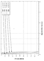
9 shows results of a first deposition experiment.
10 shows measurements of backside deposition thicknesses on a number of unclamped substrates on the pedestal of the process chamber as a function of chamber accumulation.
11 shows measurements of backside deposition thicknesses on multiple clamped substrates on an ESC in a process chamber as a function of chamber accumulation.
12 shows the mathematically modeled areas of deposition on the back side of the substrates.
이하의 기술에서, 제시된 개념들의 완전한 이해를 제공하기 위해 수많은 구체적 상세들이 제시된다. 제시된 개념들은 이들 구체적인 상세들 중 일부 또는 전부가 없이 실시될 수도 있다는 것이 자명할 것이다. 다른 예들에서, 공지된 프로세스 동작들은 기술된 개념들을 불필요하게 모호하게 하지 않기 위해 상세히 기술되지 않았다. 일부 개념들이 구체적인 실시예들과 함께 기술될 것이지만, 이들 실시예들은 제한하는 것으로 의도되지 않았다는 것이 이해될 것이다. In the following description, numerous specific details are set forth to provide a thorough understanding of the concepts presented. It will be apparent that the concepts presented may be practiced without some or all of these specific details. In other examples, well-known process operations have not been described in detail in order not to unnecessarily obscure the described concepts. While some concepts will be described in conjunction with specific embodiments, it will be understood that these embodiments are not intended to be limiting.
일부 타입들의 반도체 프로세싱에서, 이 프로세싱 동안 그 위에 웨이퍼가 배치될 수도 있는 페데스탈 또는 지지 구조체를 가질 수도 있는 프로세싱 챔버 내에서 웨이퍼 또는 기판이 프로세싱된다. 본 명세서에서, 용어들 "반도체 웨이퍼", "웨이퍼", "기판", "웨이퍼 기판", 및 "부분적으로 제조된 집적 회로"는 상호교환가능하게 사용된다. 당업자는 용어 "부분적으로 제조된 집적 회로"가 그 위에 집적 회로 제조의 많은 단계들 중 임의의 단계 동안 실리콘 웨이퍼를 지칭할 수 있다는 것을 이해할 것이다. 반도체 디바이스 산업계에 사용된 웨이퍼 또는 기판은 통상적으로 200 ㎜, 또는 300 ㎜, 또는 450 ㎜의 직경을 갖는다. 이하의 상세한 기술은 본 발명이 이러한 웨이퍼를 사용하여 구현된다는 것을 가정한다. 그러나, 본 발명은 이렇게 제한되지 않는다. 워크피스는 다양한 형상들, 사이즈들, 및 재료들일 수도 있다. 반도체 웨이퍼들에 더하여, 본 발명의 장점을 취할 수도 있는 다른 워크피스들은 인쇄 회로 기판들, 자기 기록 매체, 자기 기록 센서들, 미러들, 광학 엘리먼트들, 마이크로-기계 디바이스들, 등과 같은 다양한 물품들을 포함한다. In some types of semiconductor processing, a wafer or substrate is processed in a processing chamber that may have a pedestal or support structure on which the wafer may be placed during this processing. In this specification, the terms "semiconductor wafer", "wafer", "substrate", "wafer substrate", and "partially fabricated integrated circuit" are used interchangeably. One of ordinary skill in the art will understand that the term “partially fabricated integrated circuit” may refer to a silicon wafer during any of the many stages of integrated circuit fabrication thereon. Wafers or substrates used in the semiconductor device industry typically have a diameter of 200 mm, or 300 mm, or 450 mm. The detailed description below assumes that the present invention is implemented using such a wafer. However, the present invention is not so limited. The workpiece may be of various shapes, sizes, and materials. In addition to semiconductor wafers, other workpieces that may take advantage of the present invention include various articles such as printed circuit boards, magnetic recording media, magnetic recording sensors, mirrors, optical elements, micro-mechanical devices, etc. Include.
반도체 프로세싱은 "CVD" (chemical vapor deposition), "PECVD" (plasma-enhanced CVD), "ALD" (atomic layer deposition), 저압 CVD, 초고 (ultra-high) CVD, "PVD" (physical vapor deposition), 및 "CFD" (conformal film deposition) 와 같이, 기판 상으로 막의 하나 이상의 층들의 증착을 포함할 수도 있다. 예를 들어, 일부 CVD 프로세스들은 하나 이상의 가스 반응물질들을 반응기 내로 흘림으로써 웨이퍼 표면 상에 막을 증착할 수도 있고, 이는 막 전구체들 및 부산물들을 형성한다. 전구체들은 웨이퍼 표면으로 이송되어, 이들은 웨이퍼에 의해 흡착되고, 웨이퍼 내로 확산되고, 그리고 화학 반응들에 의해 웨이퍼 상에 증착되고, 이는 표면으로부터 그리고 반응기로부터 제거되는 부산물들을 또한 생성한다. 또 다른 예를 들면, 일부 증착 프로세스들은 복수의 막 증착 사이클들을 수반하고, 각각은 "이산적인" 막 두께를 생성한다. ALD는 이러한 일 막 증착 방법이지만, 막의 박층들을 놓고 (put down) 반복되는 순차적인 상황에 사용된 임의의 기법이 복수의 증착 사이클들을 수반하는 것을 알 수도 있다.Semiconductor processing is "CVD" (chemical vapor deposition), "PECVD" (plasma-enhanced CVD), "ALD" (atomic layer deposition), low pressure CVD, ultra-high CVD, "PVD" (physical vapor deposition). And deposition of one or more layers of a film onto a substrate, such as "CFD" (conformal film deposition). For example, some CVD processes may deposit a film on the wafer surface by flowing one or more gaseous reactants into the reactor, which form film precursors and by-products. Precursors are transferred to the wafer surface, which are adsorbed by the wafer, diffused into the wafer, and deposited on the wafer by chemical reactions, which also produce byproducts that are removed from the surface and from the reactor. As another example, some deposition processes involve multiple film deposition cycles, each producing a "discrete" film thickness. ALD is one such film deposition method, but it may be seen that any technique used in a sequential situation where thin layers of a film are put down and repeated involves multiple deposition cycles.
디바이스 및 피처들 사이즈가 반도체 산업계에서 계속해서 축소됨에 따라, 그리고 또한 3D 디바이스들 구조들이 IC (integrated circuit) 설계에서 보다 일반적이 됨에 따라, 박형의 컨포멀한 (conformal) 막들 (비평면형이더라도, 아래에 놓인 구조의 형상에 대해 균일한 두께를 갖는 재료의 막들) 을 증착하는 능력은 점점 중요해진다. ALD는 ALD의 단일 사이클이 단지 재료의 단일 박층을 증착하고, 막 형성 화학 반응 자체 이전에 기판 표면 상에 흡착할 수도 있는 하나 이상의 막 전구체 반응물질들의 양으로 두께가 제한된다는 (즉, 흡착이 제한되는 층을 형성) 사실로 인해 박형의 컨포멀한 막들의 증착에 잘 맞는 (well-suited) 막 형성 기법이다. 복수의 "ALD 사이클들"은 나중에 목표된 두께의 막을 구축하기 위해 사용될 수도 있고, 층 각각이 박형이고 컨포멀하기 때문에 발생되는 막은 아래에 놓인 디바이스들 구조의 형상을 실질적으로 따른다 (conform). 특정한 실시예들에서, ALD 사이클 각각은 다음의 단계들을 포함한다:As device and feature sizes continue to shrink in the semiconductor industry, and also as 3D device structures become more common in integrated circuit (IC) design, thin conformal films (even if non-planar, below) The ability to deposit films of material having a uniform thickness for the shape of the underlying structure) becomes increasingly important. ALD is limited in thickness to the amount of one or more film precursor reactants that a single cycle of ALD only deposits a single thin layer of material and may adsorb onto the substrate surface prior to the film formation chemistry itself (i.e., adsorption is limited. In fact, it is a well-suited film formation technique for the deposition of thin conformal films. A plurality of “ALD cycles” may later be used to build a film of a desired thickness, and the resulting film substantially conforms to the shape of the underlying devices structure because each layer is thin and conformal. In certain embodiments, each ALD cycle includes the following steps:
1. 제 1 전구체로 기판 표면의 노출.1. Exposure of the substrate surface with a first precursor.
2. 기판이 위치되는 반응 챔버의 퍼지.2. Purging of the reaction chamber where the substrate is placed.
3. 통상적으로, 플라즈마 및/또는 제 2 전구체를 사용하여, 기판 표면의 반응의 활성화.3. Activation of the reaction of the substrate surface, typically using plasma and/or a second precursor.
4. 기판이 위치되는 반응 챔버의 퍼지.4. Purging of the reaction chamber where the substrate is placed.
도 1은 임의의 수의 프로세스들을 사용하여 반도체 기판들 상에 막들을 증착하기 위한 기판 프로세싱 장치를 도시한다. 도 1의 장치 (100) 는 진공 펌프 (130) 에 의해 진공 하에 유지될 수도 있는 내부 볼륨 내 단일 기판 홀더 (118) (예를 들어, 페데스탈 또는 ESC) 와 함께 단일 프로세싱 챔버 (110) 를 갖는다. 또한, (예를 들어) 막 전구체들, 캐리어 가스 및/또는 퍼지 가스 및/또는 프로세스 가스, 이차 반응물질들, 등의 전달을 위해 가스 전달 시스템 (102) 및 샤워헤드 (104) 가 챔버에 유체적으로 커플링된다. 프로세싱 챔버 내에서 플라즈마를 생성하기 위한 장비가 또한 도 1에 도시된다. 도 1에 개략적으로 도시된 장치는 일반적으로 ALD를 수행하지만, 다른 막 증착 동작들, 예컨대 종래의 CVD, PECVD (particularly plasma enhanced CVD) 를 수행하기 위해 조정될 수도 있다.1 shows a substrate processing apparatus for depositing films on semiconductor substrates using any number of processes. The
간략함을 위해, 프로세싱 장치 (100) 는 저압 분위기를 유지하기 위한 프로세스 챔버 바디 (110) 를 갖는 독립형 프로세스 스테이션으로서 도시된다. 그러나, 본 명세서에 기술된 바와 같이 복수의 프로세스 스테이션들이 공통 프로세스 툴 분위기에―예를 들어, 공통 반응 챔버 내에―포함될 수도 있다는 것이 인식될 것이다. 예를 들어, 도 2는 멀티-스테이션 프로세싱 툴의 구현예를 도시하고 이하에 더 상세히 논의된다. 또한, 일부 구현예들에서, 본 명세서에 상세히 논의된 것을 포함하는, 프로세싱 장치 (100) 의 하나 이상의 하드웨어 파라미터들이 하나 이상의 시스템 제어기들에 의해 프로그램적으로 조정될 수도 있다는 것이 인식될 것이다.For simplicity, the
프로세싱 장치 (100) 는 분배 샤워헤드 (104) 로 액체들 및/또는 가스들을 포함할 수도 있는, 프로세스 가스들을 전달하기 위해 가스 전달 시스템 (102) 과 유체로 연통한다. 가스 전달 시스템 (102) 은 샤워헤드 (104) 로 전달을 위해, 프로세스 가스들을 블렌딩 (blending) 및/또는 컨디셔닝하기 (conditioning) 위한 혼합 용기 (mixing vessel) (106) 를 포함한다. 하나 이상의 혼합 용기 유입구 밸브들 (108 및 108A) 은 프로세스 가스들의 혼합 용기 (106) 로의 도입을 제어할 수도 있다.The
일부 반응물질들이 기화 및 프로세스 챔버 (110) 로 후속하여 전달하기 전에 액체 형태로 저장될 수도 있다. 도 1의 구현예는 혼합 용기 (106) 로 공급될 액체 반응물질을 기화시키기 위한 기화 지점 (112) 을 포함한다. 일부 구현예들에서, 기화 지점 (112) 은 가열된 액체 주입 모듈일 수도 있다. 일부 구현예들에서, 기화 지점 (112) 은 기화기일 수도 있다. 또 다른 구현예들에서, 기화 지점 (112) 은 프로세스 스테이션으로부터 제거될 수도 있다. 일부 구현예들에서, 기화 지점 (112) 의 업스트림에 LFC (liquid flow controller) 가 기화 및 프로세싱 챔버 (110) 로의 전달을 위해 액체의 대량 플로우를 제어하기 위해 제공될 수도 있다.Some reactants may be stored in liquid form prior to vaporization and subsequent delivery to the
샤워헤드 (104) 는 프로세스 스테이션에서 기판 (114) 을 향해 프로세스 가스들 및/또는 반응물질들 (예를 들어, 막 전구체들) 을 분배하고, 이의 플로우는 샤워헤드로부터 업스트림의 하나 이상의 밸브들 (예를 들어, 밸브들 (108, 108A, 116)) 에 의해 제어된다. 도 1에 도시된 구현예에서, 기판 (114) 은 샤워헤드 (104) 밑에 위치되고, ESC (118) 상에 놓인 것으로 도시된다. 샤워헤드 (104) 는 임의의 적합한 형상을 가질 수도 있고, 기판 (114) 으로 프로세스 가스들을 분배하기 위해 임의의 적합한 수 및 배열의 포트들을 가질 수도 있다. 2 이상의 스테이션들을 사용하는 일부 구현예들에서 가스 전달 시스템 (102) 은, 가스가 일 스테이션으로 흐를 수도 있지만 또 다른 스테이션으로는 흐르지 않도록, 스테이션 각각으로 프로세스 가스들 및/또는 반응물질들의 플로우를 독립적으로 제어할 수 있는, 샤워헤드로부터 업스트림에 밸브들 또는 다른 플로우 제어 구조체들을 포함한다. 더욱이, 가스 전달 시스템 (102) 은 상이한 스테이션들로 제공된 가스 조성들이 상이하도록; 예를 들어, 가스 컴포넌트의 분압이 동시에 스테이션들 사이에서 가변할 수도 있도록, 멀티-스테이션 장치의 스테이션 각각으로 전달된 프로세스 가스들 및/또는 반응물질들을 독립적으로 제어하도록 구성될 수도 있다.The
볼륨 (120) 이 샤워헤드 (104) 밑에 위치된다. 일부 구현예들에서, ESC (118) 은 기판 (114) 을 볼륨 (120) 에 노출하고 그리고/또는 볼륨 (120) 의 체적을 가변시키도록 상승되거나 하강될 수도 있다. 선택가능하게, ESC (118) 은 볼륨 (120) 내에서 프로세스 압력, 반응물질 농도, 등을 조절하기 위해 증착 프로세스의 부분들 동안 하강 및/또는 상승될 수도 있다.A
도 1에서, 샤워헤드 (104) 및 ESC (118) 은 플라즈마에 전력공급하기 위해 RF 전력 공급부 (122) 및 매칭 네트워크 (124) 에 전기적으로 접속된다. 일부 구현예들에서, 플라즈마 에너지는 (예를 들어, 적절한 머신 판독가능 인스트럭션들 및/또는 제어 로직을 갖는 시스템 제어기를 통해) 프로세스 스테이션 압력, 가스 농도, RF 소스 전력, RF 소스 주파수, 및 플라즈마 전력 펄스 타이밍 중 하나 이상을 제어함으로써 제어될 수도 있다. 예를 들어, RF 전력 공급부 (122) 및 매칭 네트워크 (124) 는 목표된 조성의 라디칼 종을 갖는 플라즈마를 형성하도록 임의의 적합한 전력에서 동작될 수도 있다. 유사하게, RF 전력 공급부 (122) 는 임의의 적합한 주파수 및 전력의 RF 전력을 제공할 수도 있다. 장치 (100) 는 또한 정전 클램핑력을 생성하고 ESC (118) 및 기판 (114) 으로 제공하기 위해 ESC (118) 로 DC 전류를 제공하도록 구성되는 DC 전력 공급부 (126) 를 포함한다. ESC (118) 는 또한 기판 (114) 을 가열 및/또는 냉각하도록 구성된 하나 이상의 온도 제어 엘리먼트들 (128) 을 가질 수도 있다. In Fig. 1, the
일부 구현예들에서, 장치는 IOC (input/output control) 인스트럭션들의 시퀀스를 통해 제어 인스트럭션들을 제공할 수도 있는, 시스템 제어기의 적절한 하드웨어 및/또는 적절한 머신-판독가능 인스트럭션들로 제어된다. 일 예에서, 플라즈마 점화 또는 유지를 위해 플라즈마 조건들을 설정하기 위한 인스트럭션들은 프로세스 레시피의 플라즈마 활성화 레시피의 형태로 제공된다. 일부 경우들에서, 프로세스 레시피들은 프로세스에 대한 모든 인스트럭션들이 그 프로세스와 동시에 실행되도록 순차적으로 배열될 수도 있다. 하나 이상의 플라즈마 파라미터들을 설정하기 위한 인스트럭션들은 플라즈마 프로세스에 선행하는 레시피에 포함될 수도 있다. 예를 들어, 제 1 레시피는 불활성 가스 (예를 들어, 헬륨) 및/또는 반응물질 가스의 플로우 레이트를 설정하기 위한 인스트럭션들, 플라즈마 생성기를 전력 설정점으로 설정하기 위한 인스트럭션들, 및 제 1 레시피에 대한 시간 지연 인스트럭션들을 포함할 수도 있다. 제 2, 후속 레시피는 플라즈마 생성기를 인에이블하기 위한 인스트럭션들 및 제 2 레시피에 대한 시간 지연 인스트럭션들을 포함할 수도 있다. 제 3 레시피는 플라즈마 생성기를 디스에이블하기 위한 인스트럭션들 및 제 3 레시피에 대한 시간 지연 인스트럭션들을 포함할 수도 있다. 이들 레시피들은 본 개시의 범위 내에서 임의의 적합한 방식으로 더 세분되고 그리고/또는 반복될 수도 있다는 것이 인식될 것이다. In some implementations, the device is controlled with appropriate hardware and/or suitable machine-readable instructions of the system controller, which may provide control instructions through a sequence of input/output control (IOC) instructions. In one example, instructions for setting plasma conditions for plasma ignition or maintenance are provided in the form of a plasma activation recipe of a process recipe. In some cases, process recipes may be arranged sequentially so that all instructions for a process are executed concurrently with the process. Instructions for setting one or more plasma parameters may be included in a recipe preceding the plasma process. For example, the first recipe includes instructions for setting the flow rate of an inert gas (e.g. helium) and/or reactant gas, instructions for setting the plasma generator to a power set point, and a first recipe. It may include time delay instructions for. The second, subsequent recipe may include instructions for enabling the plasma generator and time delay instructions for the second recipe. The third recipe may include instructions for disabling the plasma generator and time delay instructions for the third recipe. It will be appreciated that these recipes may be further subdivided and/or repeated in any suitable manner within the scope of this disclosure.
상기 기술된 바와 같이, 하나 이상의 프로세스 스테이션들이 멀티-스테이션 기판 프로세싱 툴에 포함될 수도 있다. 도 2는 예시적인 멀티-스테이션 기판 프로세싱 장치를 도시한다. 다양한 효율들이 장비 가격 및 동작 비용들, 뿐만 아니라 상승된 쓰루풋에 대해 도 2에 도시된 것과 같은 멀티-스테이션 프로세싱 장치의 사용을 통해 달성될 수도 있다. 예를 들어, 단일 진공 펌프가 모든 4 개의 프로세스 스테이션들에 대해 소비된 프로세스 가스들, 등을 배기함으로써 모든 4 개의 프로세스 스테이션들에 대한 단일 고진공 분위기를 생성하도록 사용될 수도 있다. 구현예에 따라, 프로세스 스테이션 각각은 가스 전달을 위해 고유의 전용 샤워헤드를 가질 수도 있지만, 동일한 가스 전달 시스템을 공유할 수도 있다. 유사하게, 플라즈마 생성기 장비의 특정한 엘리먼트들이 프로세스 스테이션들 (예를 들어, 전력 공급부들) 사이에 공유될 수도 있지만, 구현예에 따라, (예를 들어, 샤워헤드들이 플라즈마-생성 전기 전위들을 인가하기 위해 사용된다면) 특정한 양태들이 프로세스 스테이션-특정일 수도 있다. 다시 한번, 이러한 효율들이 또한 반응 챔버 당 2, 3, 5, 6, 7, 8, 9, 10, 11, 12, 13, 14, 15, 또는 16, 또는 보다 많은 프로세스 스테이션들과 같은 프로세싱 챔버 당 보다 많거나 보다 적은 프로세스 스테이션들을 사용함으로써 보다 큰 정도 또는 보다 적은 정도로 달성될 수도 있다는 것이 이해된다. As described above, one or more process stations may be included in a multi-station substrate processing tool. 2 shows an exemplary multi-station substrate processing apparatus. Various efficiencies may be achieved through the use of a multi-station processing apparatus as shown in FIG. 2 for equipment cost and operating costs, as well as for increased throughput. For example, a single vacuum pump may be used to create a single high vacuum atmosphere for all four process stations by evacuating spent process gases, etc. for all four process stations. Depending on the implementation, each process station may have its own dedicated showerhead for gas delivery, but may share the same gas delivery system. Similarly, certain elements of the plasma generator equipment may be shared between process stations (e.g., power supplies), but depending on the implementation (e.g., showerheads apply plasma-generated electrical potentials). If used for) certain aspects may be process station-specific. Once again, these efficiencies also per processing chamber, such as 2, 3, 5, 6, 7, 8, 9, 10, 11, 12, 13, 14, 15, or 16, or more process stations per reaction chamber. It is understood that a greater or lesser degree may be achieved by using more or fewer process stations.
도 2의 기판 프로세싱 장치 (200) 는 복수의 기판 프로세스 스테이션들을 포함하는 단일 기판 프로세싱 챔버 (210) 를 채용하고, 기판 프로세스 스테이션 각각은 그 프로세스 스테이션의 웨이퍼 홀더, 예를 들어, 페데스탈 또는 ESC에 홀딩된 기판 상에서 프로세싱 동작들을 수행하기 위해 사용될 수도 있다. 이 특정한 구현예에서, 멀티-스테이션 기판 프로세싱 장치 (200) 는 4 개의 프로세스 스테이션들 (231, 232, 233, 및 234) 을 갖는 것으로 도시된다. 다른 유사한 멀티-스테이션 프로세싱 장치들이 구현예, 그리고 예를 들어, 병렬 웨이퍼 프로세싱의 목표된 레벨, 사이즈/공간 제약들, 비용 제약들, 등에 따라 보다 많거나 보다 적은 프로세싱 스테이션들을 가질 수도 있다. 기판 핸들러 로봇 (236) 및 제어기 (238) 가 또한 도 2에 도시된다. The
도 2에 도시된 바와 같이, 멀티-스테이션 프로세싱 툴 (200) 은 기판 로딩 포트 (240), 및 카세트로부터 포드 (242) 를 통해 로딩된 기판들을 대기 포트 (240) 를 통해 프로세싱 챔버 (210) 내로, 그리고 4 개의 스테이션들 (231, 232, 233, 및 234) 중 하나 상으로 이동시키도록 구성된 로봇 (236) 을 갖는다.As shown in FIG. 2, the
도 2에 도시된 도시된 프로세싱 챔버 (210) 는 4 개의 프로세스 스테이션들 (231, 232, 233, 및 234) 을 제공한다. RF 전력은 RF 전력 시스템 (222) 에서 생성되고 스테이션들 (231, 232, 233, 또는 234) 각각으로 분배되고, 유사하게, DC 전력 소스 (226) 가 스테이션 각각으로 분배된다. RF 전력 시스템은 하나 이상의 RF 전력 소스들, 예를 들어, HFRF (high frequency) 및 LFRF (low frequency) 소스, 임피던스 매칭 모듈들, 및 필터들을 포함할 수도 있다. 특정한 구현예에서, 전력 소스는 고 주파수 또는 저 주파수 소스만으로 제한될 수도 있다. RF 전력 시스템의 분배 시스템은 반응기를 중심으로 대칭일 수도 있고 고 임피던스를 가질 수도 있다. 이 대칭 및 임피던스는 스테이션 각각으로 전달될 대략 동일한 전력의 양들을 발생시킨다. The illustrated
도 2는 또한 프로세스 툴 (200) 및 이의 프로세스 스테이션들의 프로세스 조건들 및 하드웨어 상태들을 제어하도록 채용된 시스템 제어기 (238) 의 구현예를 도시한다. 시스템 제어기 (238) 는 하나 이상의 메모리 디바이스들 (244), 하나 이상의 대용량 저장 디바이스들 (246), 및 하나 이상의 프로세서들 (248) 을 포함할 수도 있다. 프로세서 (248) 는 하나 이상의 CPU들, ASIC들, 범용 컴퓨터(들) 및/또는 특수 목적 컴퓨터(들), 하나 이상의 아날로그 입력/출력 접속부(들) 및/또는 디지털 입력/출력 접속부(들), 하나 이상의 스텝퍼 모터 제어기 보드(들), 등을 포함할 수도 있다. 2 also shows an implementation of a
시스템 제어기 (238) 는 프로세서 (248) 상의 머신-판독가능 시스템 제어 인스트럭션들 (250) 을 실행할 수도 있고, 일부 구현예들에서, 시스템 제어 인스트럭션들 (250) 은 대용량 저장 디바이스 (246) 로부터 메모리 디바이스 (244) 내로 로딩된다. 시스템 제어 인스트럭션들 (250) 은 타이밍, 가스 및 액체 반응물질들의 혼합물, 챔버 및/또는 스테이션 압력, 챔버 및/또는 스테이션 온도, 웨이퍼 온도, 타깃 전력 레벨들, RF 전력 레벨들, RF 노출 시간, 기판을 클램핑하기 위한 DC 전력 및 지속기간, 기판 페데스탈, 척 및/또는 서셉터 (susceptor) 위치, 스테이션 각각에서 플라즈마 형성 (상기 논의된 바와 같이, 하나 이상의 스테이션들에서 독립적인 플라즈마 형성을 포함할 수도 있음) 및 프로세스 툴 (200) 에 의해서 수행된 특정한 프로세스의 다른 파라미터들을 포함할 수도 있다. 이들 프로세스들은 이로 제한되는 것은 아니지만, 기판들 상에 막의 증착과 관련된 프로세스들을 포함하는 다양한 타입들의 프로세스들을 포함할 수도 있다. 시스템 제어 인스트럭션들 (258) 은 임의의 적합한 방식으로 구성될 수도 있다. The
프로세싱 동안 기판 이동은 기판의 프로세싱, 예컨대 증착된 층들에 부정적인 영향을 줄수도 있고, 기판을 인덱싱하고 이동시키기 위한 반도체 프로세싱 툴의 능력에 부정적인 영향을 줄 수도 있기 때문에, 프로세싱의 다양한 양태들 동안 웨이퍼를 고정된 위치에 유지하는 것이 바람직할 수도 있다. Because substrate movement during processing may negatively affect the processing of the substrate, e.g., deposited layers, and may negatively affect the ability of a semiconductor processing tool to index and move the substrate, the wafer may be removed during various aspects of processing. It may be desirable to keep it in a fixed position.
웨이퍼가 정전 척 (ESC) 에 의해 반도체 프로세싱 챔버 내 제자리에 고정될 수도 있다. 프로세싱 동작들의 결과로서 정전기적으로 대전될 수도 있는, 클램핑 전극(들) 및 웨이퍼가 용량성 회로로서 작용하도록, 일부 ESC들은 ESC 내 하나 이상의 클램핑 전극들에 단일 "DC" (direct current) 전압을 인가함으로써 웨이퍼를 제자리에 홀딩하고, 용량성 회로는 챔버 내 플라즈마의 존재에 의해 완성될 수도 있다. 클램핑 전극(들)은 웨이퍼의 전체 평면에 평행하고, 종종 웨이퍼 사이즈와 잘 맞는 영역에 걸쳐 연장하는, 통상적으로 박형, 평면형 구조체들이다. 용량성 효과로 인해 발생하는 정전력은 클램핑력을 제공한다. 이러한 구성은 소위 "단극성 (monopolar)"이라고 할 수도 있다. The wafer may be held in place in the semiconductor processing chamber by an electrostatic chuck (ESC). Some ESCs apply a single "direct current" (DC) voltage to one or more clamping electrodes in the ESC so that the clamping electrode(s) and wafer, which may be electrostatically charged as a result of processing operations, act as a capacitive circuit. This holds the wafer in place, and the capacitive circuit may be completed by the presence of plasma in the chamber. The clamping electrode(s) are typically thin, planar structures that are parallel to the entire plane of the wafer and often extend over an area that fits the wafer size. The static power generated due to the capacitive effect provides the clamping force. This configuration can also be called "monopolar".
ESC들은 프로세싱 동안 플라즈마 분위기들을 생성하지 않는 또한 챔버들에서 사용될 수도 있다. 이러한 구현예들에서, 플라즈마는 완전한 용량성 회로에 의존할 수 없고 ESC 전극들은 대신 하나 이상의 캐소드들 및 하나 이상의 애노드들을 포함할 수도 있다. 애노드들 및 캐소드들은 웨이퍼를 향해 대면하는 ESC의 상이한 영역들을 점유할 수도 있고, 예를 들어, 웨이퍼 또는 애노드 또는 캐소드 아래 마주보는 반원형 영역들을 점유하는 애노드 및 캐소드는 애노드로서 작용하는 웨이퍼 아래 중심 원형 전극 및 동심형 외측 전극으로서 구성된다. 이러한 ESC들의 애노드 및 캐소드는 ESC 내에서 서로로부터 전기적으로 절연되지만, 웨이퍼가 ESC 상에 위치될 때, 웨이퍼는 2 개의 용량성 회로들을 완성한다―하나는 웨이퍼가 ESC 캐소드에 대해 애노드이고, 그리고 웨이퍼가 ESC 애노드에 대해 캐소드이다. ESCs may also be used in chambers that do not create plasma atmospheres during processing. In such implementations, the plasma cannot rely on a fully capacitive circuit and the ESC electrodes may instead include one or more cathodes and one or more anodes. The anodes and cathodes may occupy different regions of the ESC facing towards the wafer, e.g., the anode and cathode occupying the opposite semicircular regions under the wafer or anode or cathode are the central circular electrode under the wafer acting as the anode. And a concentric outer electrode. The anode and cathode of these ESCs are electrically isolated from each other in the ESC, but when the wafer is placed on the ESC, the wafer completes two capacitive circuits-one is the anode to the ESC cathode, and the wafer Is the cathode for the ESC anode.
ESC들은 클램핑 전극(들) 과 웨이퍼 사이에 개재된 유전체 층 또는 다른 절연체를 가질 수도 있고; 이 유전체 또는 절연 층은 클램핑 전극(들)과 용량성 회로(들)의 1/2 즉, 웨이퍼 사이에서 쇼트 회로를 방지하도록 역할하고, ESC 및 웨이퍼에 의해 형성된 용량성 회로의 용량성 특징들을 좌우하는 갭을 규정한다. 프로세싱 분위기로의 노출로부터 전극들을 보호하기 위해 유전체 또는 절연 재료 내에 전극을 임베딩하는 (embed) 것이 일반적이다. ESCs may have a dielectric layer or other insulator interposed between the clamping electrode(s) and the wafer; This dielectric or insulating layer serves to prevent short circuits between the clamping electrode(s) and the capacitive circuit(s), i.e. between the wafer, and influences the capacitive characteristics of the capacitive circuit formed by the ESC and the wafer. To define the gap. It is common to embed the electrode in a dielectric or insulating material to protect the electrodes from exposure to the processing atmosphere.
일부 ESC들은 또한 리프트 핀들로 하여금 ESC를 통해 연장하고 ESC로부터 웨이퍼를 리프팅하게 하는 리프트 핀 홀들을 포함할 수도 있다. ESC 리프트 핀들은 일 위치에서 ESC 리프트 핀들이 ESC를 지나 연장하지 않도록 ESC 리프트 핀 내로 완전히 수축되도록 (retract) 구성될 수도 있다. 이들 리프트 핀들 및 다른 것들보다도 이들의 대응하는 홀들은 로봇 엔드 이펙터 또는 다른 기계적 디바이스로 하여금 ESC와 콘택트하지 않고 그리고/또는 간섭하지 않고 ESC로부터 웨이퍼를 위치시키고 그리고/또는 제거하게 한다. Some ESCs may also include lift pin holes that allow the lift pins to extend through and lift the wafer from the ESC. The ESC lift pins may be configured to retract completely into the ESC lift pin so that the ESC lift pins do not extend past the ESC in one position. These lift pins and their corresponding holes above all others allow a robot end effector or other mechanical device to position and/or remove a wafer from the ESC without contacting and/or interfering with the ESC.
많은 현재 ESC들 및 웨이퍼 지지 페데스탈들 (예를 들어, 클램핑력을 사용하지 않는 페데스탈들) 이 다수의 이유들로 목표되지 않은, 웨이퍼의 후면에 의도치 않은 증착을 허용한다. 예를 들어, 프로세싱 챔버에서 증착 동안, 막은 웨이퍼의 전면 상뿐만 아니라, 웨이퍼의 후면 상에도 증착될 수 있다. ALD (atomic layer deposition) 과 같은 컨포멀한 증착 기법들에서, 예를 들어, 막은 연속적인 도즈 및 활성화 단계들에 의해 층단위로 (layer by layer) 증착될 수 있다. 많은 ALD 프로세싱 챔버들에서, 전구체 가스들이 웨이퍼로 지향될 수 있고 전구체 가스들이 모노레이어를 형성하도록 웨이퍼의 표면 상에 화학흡착할 수 있다. 모노레이어와 반응하는 부가적인 전구체 가스들이 도입될 수 있고, 퍼지 가스가 과잉 전구체들 및 가스성 반응 부산물들을 제거하도록 후속하여 도입될 수 있다. 전구체 가스들이 오버랩 없이 교번적으로 펄싱할 수 있고, 사이클들이 적합한 두께의 막을 형성하는 것이 목표되는 바에 따라 수회 반복될 수 있다. Many current ESCs and wafer support pedestals (eg, pedestals that do not use clamping force) allow unintended deposition on the back side of the wafer, which is not targeted for a number of reasons. For example, during deposition in a processing chamber, a film may be deposited on the front side of the wafer as well as on the back side of the wafer. In conformal deposition techniques such as atomic layer deposition (ALD), for example, a film may be deposited layer by layer by successive dose and activation steps. In many ALD processing chambers, precursor gases can be directed to the wafer and precursor gases can chemisorb onto the surface of the wafer to form a monolayer. Additional precursor gases that react with the monolayer may be introduced, and a purge gas may be subsequently introduced to remove excess precursors and gaseous reaction by-products. The precursor gases can pulse alternately without overlap, and the cycles can be repeated several times as desired to form a film of suitable thickness.
그러나, 증착 프로세스 동안, 프로세스 가스들, 예컨대 ALD에서 전구체 가스들이 증착이 목표되지 않는, 웨이퍼의 표면들, 예를 들어, 웨이퍼의 후면 상에 증착될 수 있다. ALD가 표면-기반 증착 프로세스이기 때문에, 막은 프로세싱 챔버의 임의의 액세스가능한 막 상에 증착될 수 있다. 따라서, 웨이퍼의 후면에 액세스하는 모든 갭은 가스들로 하여금 후면으로 흐르도록 허용할 수 있다. 후면 상의 막은 도즈 단계 동안 전구체 가스들의 이송에 의해 생성될 수 있고, 활성화 단계 동안 전구체 가스들의 반응이 발생할 수 있다. 일부 구현예들에서, 웨이퍼의 외측 에지에서 전면 막만큼 두꺼운 원치 않은 막의 링이 웨이퍼의 후면에서 전개될 수 있고 웨이퍼의 외측 에지로부터 내측으로 5 ㎜보다 크게 연장할 수 있다 .However, during the deposition process, process gases, such as precursor gases in ALD, may be deposited on the surfaces of the wafer, eg, the back side of the wafer, for which deposition is not desired. Because ALD is a surface-based deposition process, the film can be deposited on any accessible film in the processing chamber. Thus, any gap that accesses the back side of the wafer can allow gases to flow to the back side. The film on the back side may be produced by transport of precursor gases during the dosing step, and reaction of the precursor gases may occur during the activation step. In some implementations, a ring of undesired film as thick as the front film at the outer edge of the wafer may develop at the back side of the wafer and extend more than 5 mm inward from the outer edge of the wafer.
이러한 원치 않은 후면 증착의 단점들 중 하나는 리소그래피 동안 정렬/포커싱 문제들을 야기할 수 있다는 것이다. 목표된 패턴을 웨이퍼의 타깃 부분에 적용하기 위해, 리소그래피의 다양한 툴들이 목표된 패턴을 위해 적절한 정렬 및 포커싱을 위해 사용될 수 있다. 증착 단계 후, 막이 웨이퍼의 후면 상에 증착되면, 다양한 리소그래피 툴들이 포커스 및 정렬에 재조정을 요구할 수도 있다. 이는 웨이퍼 결함들을 야기할 수 있는 패터닝 동안 원치 않은 리소그래피 트레이스들 및 다양한 리소그래피 툴들을 재캘리브레이팅하는데 소비된 증가된 시간을 야기할 수 있다. One of the drawbacks of such unwanted backside deposition is that it can cause alignment/focusing problems during lithography. In order to apply the desired pattern to the target portion of the wafer, various tools of lithography can be used for proper alignment and focusing for the desired pattern. After the deposition step, if the film is deposited on the back side of the wafer, various lithography tools may require readjustment of focus and alignment. This can lead to increased time spent recalibrating various lithography tools and unwanted lithography traces during patterning which can lead to wafer defects.
본 명세서에 기술된 ESC들은 기판의 하측으로 가스들의 플로우를 방지하거나 감소시켜, 기판의 후면 상에 증착을 감소시키거나 실제로 제거하기 위해, 기판의 후면으로 하여금 상부 환형 시일 표면에 대고 하향으로 가압되게 (forced) 하도록 기판 상에 정전 클램핑력들을 부과하도록 구성된다. 상기 언급된 바와 같이, 컨포멀한 증착의 본질은 프로세스 가스들이 흐를 수도 있는 이들 가스들에 노출되는 기판의 임의의 표면을 포함하는, 어느 곳에서나 증착이 발생하게 한다. 프로세스 가스들 및 다른 재료가 기판의 하측으로 흐르는 것을 방지하기 위해, 기판의 하측과 평면형 평활한 상부 환형 시일 표면 사이의 시일이 기판의 하측의 에지에서 시작하고 ESC의 바디의 수직 중심 축을 향해 방사상 내측으로 연장하는 영역에서 생성될 수도 있다. 기판의 에지에서 발생하는 시일을 사용하여, 가스들 및 다른 재료가 기판 아래로 흐를 수 없다. 하향 정전 클램핑력의 인가는 기판의 하측의 에지, 및 기판의 하측의 일부로 하여금 상부 환형 시일 표면과 콘택트하고 시일을 생성하는 것을 보조할 수도 있다. The ESCs described herein cause the back side of the substrate to be pressed downward against the upper annular seal surface to prevent or reduce the flow of gases down the substrate, thereby reducing or actually eliminating deposition on the back side of the substrate. It is configured to impose electrostatic clamping forces on the substrate to be forced. As mentioned above, the nature of conformal deposition allows deposition to occur anywhere, including any surface of the substrate that is exposed to these gases through which process gases may flow. To prevent process gases and other materials from flowing down the substrate, the seal between the lower side of the substrate and the planar smooth upper annular seal surface starts at the lower edge of the substrate and radially inward toward the vertical central axis of the body of the ESC. It can also be created in a region extending to. With the seal occurring at the edge of the substrate, gases and other materials cannot flow down the substrate. The application of a downward electrostatic clamping force may assist the lower edge of the substrate, and a portion of the lower side of the substrate, to contact the upper annular seal surface and create a seal.
기판 이상의 직경을 갖는 연속적인 평면형 원형 시일 표면과 반대로, 상부 환형 시일 표면의 사용은 많은 장점들을 발생시킨다. 예를 들어, 기판이 ESC의 평면형, 원형 표면 상에 위치될 때, 공기 (또는 다른 가스) 가 이 기판이 ESC 상에 위치될 때 원형 표면과 기판 사이에 포획될 수도 있고 이는 트랩된 (trapped) 가스가 탈출할 수 있기 전에 기판으로 하여금 ESC에 대해 병진 (translate) 및/또는 회전하게, 즉, 트랩된 가스 층 (cushion of trapped gas) 을 "플로팅"하게 할 수도 있고, 이는 웨이퍼 오정렬에 의해 유발된 인덱싱 에러들 및 웨이퍼 결함들을 야기할 수 있다. 부가적으로, 재료의 의도치 않은 증착이 원형 표면의 내부 위치들 상에서 발생할 수 있고 이는 증착 동안 기판 상에 결함들을 야기할 수도 있는, 기판이 레벨 평면에 위치되는 것을 방지할 수도 있다. 원형 표면 상의 이 증착은 또한 기판과 원형 표면 사이에 갭들을 생성하거나 악화시킬 수도 있고, 이는 프로세스 가스들로 하여금 기판의 하측으로 흐르게 할 수 있고 상기 언급된 바와 같이,나중의 프로세싱 단계들에 단점들을 제공하고 궁극적으로 기판 상에 결함들, 또는 추가의 이러한 문제들을 야기할 수도 있는, 원형 표면 상의 추가 증착을 야기할 수도 있는, 후면 증착을 유발할 수 있다. 기판을 지지하고, 하향 클램핑력의 압력을 적절히 분배하고, 그리고 기판이 원치 않은 변형 및 손상을 겪는 것을 방지하기 위해, ESC는 따라서 원형 표면과 관련한 문제들을 방지하고 결국 ESC 바디의 리세스 내에 배열된 복수의 마이크로-콘택트 영역 (micro-contact area; MCA) 피처들 (이들 MCA 피처들은 이하 "MCA들"로 참조됨) 을 활용하도록 상부 환형 링을 사용할 수도 있다.As opposed to a continuous planar circular seal surface having a diameter greater than or equal to the substrate, the use of an upper annular seal surface creates many advantages. For example, when a substrate is placed on the planar, circular surface of the ESC, air (or other gas) may be trapped between the circular surface and the substrate when this substrate is placed on the ESC, which is trapped. It is also possible to cause the substrate to translate and/or rotate relative to the ESC before the gas can escape, ie “floating” the trapped gas layer, which is caused by wafer misalignment. Indexing errors and wafer defects. Additionally, undesired deposition of material may occur on internal locations of the circular surface, which may prevent the substrate from being placed in the level plane, which may cause defects on the substrate during deposition. This deposition on the circular surface may also create or worsen gaps between the substrate and the circular surface, which can cause process gases to flow underneath the substrate and, as mentioned above, introduce drawbacks to later processing steps. Can lead to backside deposition, which may lead to further deposition on the circular surface, which may provide and ultimately cause defects on the substrate, or further such problems. In order to support the substrate, to properly distribute the pressure of the downward clamping force, and to prevent the substrate from undergoing unwanted deformation and damage, the ESC thus avoids problems associated with the circular surface and eventually arranged in the recess of the ESC body. An upper annular ring may be used to utilize a plurality of micro-contact area (MCA) features (these MCA features are hereinafter referred to as “MCAs”).
본 명세서에 기술된 ESC들은 상부 환형 시일 표면과 기판의 하측 사이에 시일을 생성하고 유지하기 위해 기판 상으로 하향 정전 클램핑력을 인가하도록 구성된다. 이 하향 힘의 인가 없이, 웨이퍼 에지와 환형 시일 표면 사이에 작은 갭들이 여전히 있을 수도 있고 프로세스 가스들은 여전히 기판의 하측으로 흐를 수도 있고 원치 않은 후면 증착을 유발할 수도 있다. 예를 들어, 일부 상황들에서 중력 단독으로 가스들이 기판 밑을 흐르는 것을 방지할 수 있는 적절한 시일을 생성하지 못할 수도 있다. 일부 이러한 상황들에서, 기판 에지들이 뒤틀릴 (warped) 수도 있고 또는 기판 자체가 변형될 수도 있고, 이는 가스들로 하여금 기판의 후면으로 흐르게 할 수 있다. 더욱이, 일부 프로세싱 조건들은 다른 것들보다 공격적, 예컨대 보다 고온들에서 그리고 보다 긴 지속기간들 동안 발생할 수도 있고, 이는 기판의 에지들로 하여금 랩핑되게 하고, 가스들로 하여금 기판의 후면을 흐르게 하고 후면 증착을 유발하는 것과 같은 조건들을 생성할 수도 있다. 특히, 일부 예들에서, 웨이퍼는 웨이퍼 자체와 상이한 열 팽창 계수를 갖는 웨이퍼의 상단 측에 증착된 재료를 가질 수도 있고, 온도 변화들 동안, 웨이퍼의 두께를 가로질러 장력 변화가 발현되게 할 수도 있어서, 웨이퍼로 하여금 상단 표면에서 약간 오목한 곳을 나타내는) "디시 (dish)"가 되게 하고 웨이퍼 에지로 하여금 페데스탈로부터 약간 리프팅되게 한다.The ESCs described herein are configured to apply a downward electrostatic clamping force onto the substrate to create and hold a seal between the upper annular seal surface and the underside of the substrate. Without the application of this downward force, there may still be small gaps between the wafer edge and the annular seal surface and process gases may still flow underneath the substrate and cause unwanted backside deposition. For example, in some situations gravity alone may not create an adequate seal to prevent gases from flowing under the substrate. In some such situations, the substrate edges may be warped or the substrate itself may be deformed, which may cause gases to flow to the back side of the substrate. Moreover, some processing conditions may occur more aggressive than others, such as at higher temperatures and for longer durations, which cause the edges of the substrate to wrap, allow gases to flow through the backside of the substrate and backside deposition. You can also create conditions such as those that trigger In particular, in some examples, the wafer may have a material deposited on the top side of the wafer having a different coefficient of thermal expansion than the wafer itself, and during temperature changes, a change in tension across the thickness of the wafer may develop, It causes the wafer to become a "dish" representing a slight depression in the top surface and causes the wafer edge to lift slightly from the pedestal.
많은 기존 ESC 설계들에서, 클램핑 전극(들)은 (때때로 그 사이에 내열층과 같은 다른 층들을 갖는) ESC의 금속 베이스플레이트에 결합되는 유전체 플레이트 내에 임베딩되고; 베이스플레이트는 자주 ESC를 위한 전체 구조적 프레임워크로서 뿐만 아니라 프로세싱 챔버 내에 플라즈마 분위를 생성하기 위해 사용되는 RF (radio-frequency) 전극 모두로 기능한다. 많은 반도체 프로세싱 동작들에서, ESC는 웨이퍼를 가열 및/또는 냉각하기 위해 열 관리 컴포넌트들을 또한 포함할 수도 있다. 일부 반도체 프로세스들에서, ESC 상의 웨이퍼가 특정한 프로세싱 요건들을 만족시키기 위해, ESC 내에 임베딩된 가열 엘리먼트들을 사용하기 위해, 저온 범위로 간주될 수도 있는, 대략 30 ℃ 내지 150 ℃ 범위의 온도들, 뿐만 아니라 150 ℃ 이상, 예컨대 400 ℃까지 가열될 수도 있다. In many existing ESC designs, the clamping electrode(s) is embedded in a dielectric plate that is bonded to the metal base plate of the ESC (sometimes with other layers such as a heat resistant layer in between); The baseplate often functions both as an overall structural framework for ESCs as well as as radio-frequency (RF) electrodes used to create a plasma atmosphere within the processing chamber. In many semiconductor processing operations, the ESC may also include thermal management components to heat and/or cool the wafer. In some semiconductor processes, the wafer on the ESC has temperatures in the range of approximately 30° C. to 150° C., which may be considered a low temperature range, to use heating elements embedded in the ESC to satisfy certain processing requirements, as well as It may be heated to 150° C. or higher, for example to 400° C.
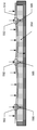
도 3은 상부 환형 시일 표면 (362), 반투명 교차-해칭으로 도시된 리세스 (364), 및 리세스 (364) 내에 배치된 복수의 "MCA들" (micro-contact areas) (366) 을 포함하는, 바디 (360) 를 갖는 예시적인 ESC (318) 의 상면도를 도시한다. 도 3의 도면은 상부 환형 시일 표면 (362) 에 또한 수직인, ESC의 수직 중심 축을 따라, 즉 평행하다. 도 3에서 알 수 있는 바와 같이, 상부 환형 시일 표면 (362) 은 리세스 (364) 둘레로 완전히 연장하는, 도면에서 이를 강조하기 위해 음영으로 도시된 원주 링이다. 상부 환형 시일 표면 (362) 은 상부 환형 시일 표면 (362) 이 방사상 두께 (372) 를 갖도록 내측 반경 (368) 및 외측 반경 (370) 에 의해 경계가 지어진다 (bound). 상부 환형 시일 표면 (362) 은 기판의 에지 및 하측 또는 후면 부분을 지지하도록 구성된다. 내측 반경 (368) 은 따라서 기판의 반경보다 작게 사이즈가 결정될 수도 있고 외측 반경 (370) 은 기판의 반경보다 크게 사이즈가 결정될 수도 있다. 예를 들어, 일부 실시예들에서, 내측 반경 (370) 은 약 142.9 ㎜ (약 5.625 인치) 또는 약 131.6 ㎜ (약 5.18 인치) 사이일 수도 있지만, 외측 반경은 약 150.6 ㎜ (또는 약 5.9275 인치) 일 수도 있다. 일부 이러한 실시예들에서, 상부 환형 시일 표면의 방사상 두께는 약 15.4 ㎜ (약 0.605 인치) 를 포함하여, 약 25 ㎜ 이하일 수도 있다. 일부 실시예들에서, 이 방사상 두께는 300 ㎜, 450 ㎜, 및 200 ㎜의 직경들을 갖는 기판들을 시일하도록 환형 시일 표면을 지지하고 가능하게 하도록 사이즈가 결정될 수도 있다. 상부 환형 시일 표면 (362) 은 적어도 부분적으로 시일이 기판의 후면과 상부 환형 시일 표면 사이에 생성되게 하도록 편평하고, 평면형이고, 평활한 표면이다. 일부 실시예들에서, 이 평활도는 약 0.2032 ㎛ (8 Ra), 이하를 포함하여, 0.8128 ㎛ (32 Ra) 이하일 수도 있다. 평탄도는 상부 환형 시일 표면의 가장 높은 곳으로부터 가장 낮은 곳까지 최대 변동인, 0.0254 ㎜ (0.001 인치) 의 최대 범위 및 환형 시일 표면의 25.4 ㎜ x 25.4 ㎜ 사각형마다 0.00254 ㎜ (1 inch x 1 inch 사각형마다 0.0001 인치) 의 국부화된 범위를 가질 수도 있다. FIG. 3 includes an upper
도 3에 도시된 바와 같이, 바디 (360) 의 리세스 (364) 는 중심 수직 축을 따라 봤을 때 상부 환형 시일 표면 (362) 보다 바디 (360) 의 수직 축의 중심에 보다 가깝게 위치된다. 상부 환형 시일 표면 (362) 은 리세스 (364) 둘레로 연장하고 적어도 부분적으로 리세스 (364) 의 경계를 짓는 것으로 간주될 수도 있다. 리세스 (364) 는 하부 리세스 표면 (374) 및 리세스 (364) 의 경계로부터 리세스 측 표면 (376) 을 포함할 수도 있다. 도 4a 및 도 4b는 도 3의 ESC 바디의 예시적인 단면 슬라이스를 도시한다. 이들 도면들은 본 명세서에 기술된 양태들을 예시하기 위해 스케일대로 도시되지 않고 수직 축으로 과장되었다. 도 4a의 도면은 수직 중심 축 (378) 에 수직이고 상부 환형 시일 표면 (362) 에 평행하다. 여기서, 바디 (360) 의 측면 슬라이스는 하부 리세스 표면 (374), 리세스 측 표면 (376), 및 상부 환형 시일 표면 (362) 을 포함하는 것으로 도시되고; MCA들은 예시를 목적으로 도시되지 않고, 이하 도 6a 내지 도 7에 기술된다. 3, the
하부 리세스 표면 (374) 은 도 4a에서 알 수 있는 바와 같이 평면형, 원형 표면일 수도 있고, 수직 중심 축 (378) 을 따라 제 1 거리 (380) 만큼 상부 환형 시일 표면 (362) 으로부터 또는 아래로 오프셋된다. 일부 실시예들에서, 하부 리세스 표면 (374) 및 상부 환형 시일 표면 (362) 은 또한 서로 평행한 것으로 간주될 수도 있다. 리세스 측 표면 (376) 은 하부 리세스 표면 (374) 둘레로 연장하는 원형 링일 수도 있고, 일부 실시예들에서, 하부 리세스 표면 (374) 에 그리고/또는 상부 환형 시일 표면 (362) 에 실질적으로 수직 (예를 들어, 직교의 +/- 5 % 이내) 일 수도 있다. 일부 실시예들에서, 하부 리세스 표면 (374) 은 도 4a에 도시된 바와 같이, 상부 환형 시일 표면 (362) 의 내측 반경 (368) 과 실질적으로 동일할 (예를 들어, 10 % 또는 약 1 % 미만) 수도 있는 반경 (386) 을 가질 수도 있다. 도 4b에서, 도 4a의 동일한 바디 (360) 가 도시되지만, 리세스 (364) 의 체적 구상적 슬라이스는 약간 음영으로 도시된다. The
일부 실시예들에서, 바디 (360) 는 단일, 모놀리식 구조체일 수도 있지만 다른 실시예들에서 복수의 부품으로 구성될 수도 있다. 예를 들어, 도 4b의 바디는 하부 리세스 표면 (374) 을 포함하는 제 1 부분 (382) 및 상부 환형 시일 표면 (362) 및 측 표면 (376) 을 포함하는 제 2 부분 (384) 을 포함할 수도 있고 제 1 거리 (380) 인 높이 및 방사상 두께 (372) 인 두께를 갖는 환형 링일 수도 있다. 제 1 부분 (382) 및 제 2 부분 (384) 이 연결, 예를 들어, 용접, 확산 본딩, 함께 기밀 연결되면, 리세스 (364) 가 형성된다. 바디는 세라믹과 같은 유전체 재료로 이루어질 수도 있고, 또는 유전체 재료로 코팅된 금속 또는 금속 합금일 수도 있다. In some embodiments, the
하부 리세스 표면 (374) 과 상부 환형 시일 표면 사이의 수직 오프셋 (380) 은 클램핑력으로 하여금 ESC 상에 위치된 기판에 인가되게 하도록 구성될 수도 있다. 도 4a를 다시 참조하면, 바디 (360) 는 기판이 ESC에 지지될 때 그리고 전력이 하나 이상의 정전 클램프 전극들 (394) 에 공급될 때 하향 클램핑력으로 하여금 기판에 인가되게 하도록 구성되는 하나 이상의 정전 클램프 전극들 (394) 을 포함한다. 기판과 하나 이상의 정전 클램프 전극들 (394) 사이의 이 클램핑력은 거리가 증가함에 따라 힘이 감소하도록 다른 인자들 보다도, 기판과 하나 이상의 정전 클램프 전극들 (394) 사이의 거리에 종속된다. 하부 리세스 표면 (374) 과 상부 환형 시일 표면 (362) 사이의 수직 오프셋 (380) 은 따라서 프로세싱 동작들 동안 기판과 ESC 사이의 클램핑력이 기판을 ESC 상의 제자리에 유지하게 인가될 수도 있도록 사이즈가 결정될 수도 있다. 일부 실시예들에서, 이 수직 오프셋 (380) 은 0이 아니고 0.0381 ㎜ (0.0015 인치), 0.0254 ㎜ (0.001 인치), 또는 0.0127 ㎜ (0.0005 인치) 이하일 수도 있다. 일부 실시예들에서, 하나 이상의 정전 클램프 전극들이 1 내지 40 Torr, 예를 들어 (0.02 psi 내지 0.8 psi) 의 정전 클램핑력 또는 압력을 인가하도록 구성될 수도 있다. 일부 실시예들에서, 바디는 하부 리세스 표면 아래에 위치되고 300 V 이상, 예컨대 600 V, 700 V, 800 V, 900 V, 및 1,000 V의 DC 전압에 접속하도록 구성되는 2 이상의 정전 클램프 전극들 (394) 을 포함할 수도 있다. 일부 실시예들에서, ESC의 RF 전극은 또한 DC 전압이 RF 전극에 인가되어 본 명세서에 기술된 정전 클램핑력을 생성하도록 정전 클램프 전극으로서 역할한다. The vertical offset 380 between the
상부 환형 시일 표면 (362) 과 함께, 복수의 MCA들은 ESC 상에 위치되는 기판을 지지하고 하향 정전 클램핑력을 받을 때 기판에 원치 않은 변형 및 압력을 방지하도록 구성된다. 일반적으로 말하면, 기판이 환형 표면 상에 위치되고 이에 의해서만 지지될 때, 기판에 대한 중력은 수직 변형이 매우 적거나 없게 한다. 반대로, 동일한 기판이 하향 클램핑력을 받을 때, 기판은 변형하게 될 수도 있고, 이는 기판 상에 결함들 및 손상을 유발할 수 있다. 유사하게, 기판이 환형 링 및 예컨대 5 또는 10과 같은 적은 복수의 MCA들에 의해 지지되면, 중력은 통상적으로 기판 상에 바람직하지 않은 압력을 유발하지 않는다. 그러나 기판에 인가된 하향력은 바람직하지 않은 변형 또는 MCA들이 기판과 콘택트하는 점 압력을 유발할 수도 있고, 이는 하향 클램핑력의 압력을 기판에 동일하고 적절하게 분배하기 충분한 수의 적절한 배열의 MCA들이 없다면 기판에 손상을 유발하거나 기판의 결함들을 발생시킬 수도 있다. Along with the upper
도 5a 및 도 5b는 환형 링에 의해 지지된 예시적인 기판의 단면도를 도시하고 도 5c는 3 개의 콘택트 영역들에 의해 지지된 도 5a의 예시적인 기판의 단면도를 도시한다. 다시, 도 4a 및 도 4b와 같이, 이들 도면들은 본 명세서에 기술된 양태들을 예시하기 위해 스케일대로 도시되지 않고 수직 축으로 과장되었다. 도 5a에서, 기판 (514) 은 환형 링 (588) 에 의해서만 지지되고; 수직 지지부들 없이 (연한 음영으로 도시된) 리세스 (564) 는 환형 링 (588) 내에 방사상으로 그리고 기판 (514) 대부분의 밑에 위치된다. 여기서, 하향 정전 클램핑력이 기판 (514) 에 인가되지 않아, 기판 (514) 의 어떠한 변형도 유발하지 않는다. 도 5b에서, 하향 정전 클램핑력이 수직 하향 화살표들로 나타낸 바와 같이 도 5a의 기판 (514) 에 인가되어, 기판 (514) 으로 하여금 제 1 변형 거리 (590) 만큼 리세스 (564) 내로 변형하게 한다. 상기 언급된 바와 같이, 이 변형은 기판 (514) 상에 결함들이 발생하게 하거나 손상을 유발할 수도 있다. 도 5c에서, 3 개의 MCA들 (566) 이 리세스 (564) 내 그리고 기판 (514) 밑에 위치되지만, 이들 MCA들 (566) 은 하향 화살표들로 예시된 하향 클램핑력의 압력이 기판을 따라 적절히 분배되지 않도록 위치되어, 기판에 원치 않는 변형뿐만 아니라 식별자 592와 함께 원으로 표시된 기판이 MCA들과 콘택트하는 점 압력을 유발한다.5A and 5B show a cross-sectional view of an exemplary substrate supported by an annular ring and FIG. 5C shows a cross-sectional view of an exemplary substrate of FIG. 5A supported by three contact regions. Again, as shown in FIGS. 4A and 4B, these drawings are not drawn to scale but exaggerated on the vertical axis to illustrate the aspects described herein. In Fig. 5A, the
도 3을 다시 참조하면, 환형 링 (362), 리세스 (364), 및 MCA들 (366) 을 포함하는 바디는 하향 클램핑력에 의해 유발된 기판 상의 부정적인 효과들을 감소시키거나 제거하도록 구성되고 배치된다. 예를 들어, (도 3에 도시된 것과 유사하게) 상부 환형 시일 표면의 방사상 두께 (372) 및 리세스 (364) 의 표면적은 다수의 인자들에 기초하여 구성될 수도 있다. 일부 실시예들에서, 기판 하측 대부분에 균일한 조건들을 제공하기 위해 기판 밑에 큰 리세스를 갖는 것이 바람직할 수도 있다. 예를 들어, 기판의 하측의 표면적의 80 %, 85 %, 95 %, 98 %, 이상인 리세스 (364) 의 표면적을 갖는 것이 유리할 수도 있다. 두 표면들 사이에 시일을 생성하기 위해, 기판 후면과 상부 환형 시일 표면 사이에 충분한 콘택트가 있도록 충분히 크게 사이즈가 결정된 방사상 두께 (372), 예를 들어, 바디의 수직 중심 축을 따라 볼 때, 기판의 에지의 원주로 하여금 상부 환형 시일 표면의 내측 원주를 둘러싸거나 둘레로 연장하도록, 충분히 작은 제 1 반경 (368) 을 갖는 것이 또한 유리할 수도 있다. 이 방사상 두께 (372) 는 또한 기판을 ESC 상으로 위치시키는 웨이퍼 핸들러들의 부정확도들 및 허용오차들을 또한 고려하면서, 기판의 인덱싱 또는 정렬 노치를 포함하여, 전체 에지 둘레를 시일하도록 충분히 두꺼워야 한다.Referring again to FIG. 3, the body comprising the
일부 실시예들에서, 복수의 MCA들 (366) 은 하부 리세스 표면 (374) 으로부터 돌출하고 하부 리세스 표면으로부터 오프셋되는 상단 표면을 갖는다. 도 6a는 MCA들과 함께 도 4a의 ESC 바디 (360) 의 예시적인 단면 슬라이스를 도시한다. 복수의 MCA들 (366) 이 하부 리세스 표면 (374) 으로부터 돌출하는 것으로 도시되고 MCA (366) 각각은 상단 표면 (396) 및 바디 (398) 를 포함한다. 일부 실시예들에서, MCA 각각의 상단 표면 (396) 은 상부 환형 시일 표면 (362) 및 MCA 각각의 상단 표면 (396) 이 하부 리세스 표면 (374) 으로부터 동일한 거리, 즉, 동일한 수직 오프셋 (380) 만큼 오프셋되도록 상부 환형 시일 표면 (362) 과 동일 평면상일 수도 있다. 도 6a에서, MCA들의 상단 표면들 (396) 은 제 1 거리 (380) 와 실질적으로 동일할 수도 있는 제 2 거리 (3100) 만큼 하부 리세스 표면 (374) 으로부터 오프셋된다. 일부 다른 실시예들에서, MCA들 (366) 의 상단 표면들 (396) 은 하부 리세스 표면 (374) 보다 낮을 수도 있고, 또는 상부 환형 시일 표면 (362) 보다 하부 리세스 표면 (374) 으로부터 보다 적게 오프셋될 수도 있다. 이는 부가적인 변형이 기판에 대한 클램핑력에 의해 유발되지 않도록 ESC 상에 위치되기 전에 볼록하거나 오목한 방식으로 이미 변형될 수도 있는 일부 기판들로부터 유리할 수도 있다. 이는 또한 기판이 평면형이더라도 누설을 방지하는 것을 도울 수도 있다. 예를 들어, 리세스 에지 근방에 단일 "고 (high)" MCA가 있다면, 상부 환형 시일 표면으로부터 리프팅될 수도 있고 그 위치에서 클램핑력은 리프팅을 극복하지 못할 수도 있다. In some embodiments, the plurality of
상부 환형 시일 표면 (362) 과 유사하게, 일부 실시예들에서 MCA 각각과 기판 사이에 균일한, 고르게 분포된 콘택트를 제공하기 위해 MCA들의 상단 표면들 (396) 이 평면형 표면들이도록 하는 것이 유리하다. 평면도 및 평탄도는 상부 환형 시일 표면에 대해 상기 기술된 바와 같이 동일할 수도 있다. MCA 각각의 바디는 하부 리세스 표면 (374) 과 상단 표면 (396) 사이에 개재될 수도 있고 예를 들어, 원형 바디, 테이퍼된 바디, 또는 사각형 바디일 수도 있다.Similar to the upper
도 7은 도 3의 ESC의 부분의 비스듬한 상세도의 일부를 도시한다. 이 도면은 이하의 도 8보다 더 확대된다. 여기서, 4 개의 MCA들 (366) 은 MCA (366) 각각이 원형, 평면형 상단 표면 (396) 을 갖고 제 2 높이 (3100) 만큼 하부 리세스 표면 (374) 으로부터 연장하는 원통형으로 도시된다. 상부 환형 시일 표면 (362) 의 단면이 또한 도시되고 제 1 거리 (380) 및 리세스 측 표면 (376) 이 식별된다. 7 shows a part of an oblique detail view of a portion of the ESC of FIG. 3. This figure is further enlarged than that of Figure 8 below. Here, the four
상기 언급된 바와 같이, MCA들은 기판으로 하향 정전 클램핑력을 고르게 분배하기 위해 사이즈가 결정되고 배치될 수도 있다. 일부 실시예들에서, 압력을 고르게 분배하기 위해 수백 또는 수천 개의 MCA들, 예컨대 2,000 개의 MCA들, 4,000 개의 MCA들, 또는 그 이상을 사용하는 것이 유리하다는 것을 알게 되었다. 이와 함께, 모든 MCA 상단 표면들 (396) 의 총 표면적이 MCA들에 의해 점유된 표면적을 포함하는 리세스 (364) 의 총 표면적의 3 % 이하인 것이 유리하다는 것을 알게 되었고; 이는 기판 상에 압력을 분배하고 감소시키는 것을 알게 되었다. 예를 들어, 바디는 (상부 환형 시일 표면 (362) 의 제 1 반경 (368) 과 동일할 수도 있는) 약 142 ㎜의 반경을 갖는 리세스를 가질 수도 있고 각각 약 0.35 ㎜의 상단 표면 반경을 갖는 4,000 개의 MCA들을 포함할 수도 있고, 63,347.1 ㎜2인 총 리세스 표면적의 약 2.4 %인 1,539.4 ㎜2의 MCA 상단 표면들의 총 표면적을 발생시킨다. As mentioned above, MCAs may be sized and placed to evenly distribute the downward electrostatic clamping force to the substrate. In some embodiments, it has been found that it is advantageous to use hundreds or thousands of MCAs, such as 2,000 MCAs, 4,000 MCAs, or more to evenly distribute the pressure. Together, it has been found advantageous to have the total surface area of all MCA top surfaces 396 to be less than 3% of the total surface area of the
리세스 내 MCA들의 배치 및 분포는 또한 기판 상에 정전 압력을 균일하게 분배하도록 구성될 수도 있다. 예를 들어, 바디의 수직 축을 따라 볼 때, MCA들은 균일하고, 대칭적으로, 그리고 서로로부터 동일하게 이격될 수도 있고, 웨이퍼에 압력을 균일하게 분배할 수도 있다. 도 8은 도 3의 원형 경계로 나타낸 바와 같이 도 3의 ESC 바디의 상세도를 도시한다. 여기서, 상부 환형 시일 표면 (362) 의 일부가 도시되고 복수의 MCA들 (366) 은 원형 표면들이고 동일하게 이격된 것으로 도시된다. 일부 실시예들에서, 복수의 MCA들은 복수의 하위-배열 패턴들, 예컨대 삼각형 패턴, 사각형 패턴, 대칭 패턴, 방사상 배열, 및 육각형 패턴으로 배치될 수도 있다. 도 8에서, MCA들은 하위-배열 삼각형 각각에 3 개의 MCA들을 갖는 삼각형인 복수의 대칭적 하위-배열들로 배치된다. 일 하위-배열 (8104) 은 점선 삼각형으로 식별되고 3 개의 간격 측정값들 8106A, 8106B, 및 8106C로, 3 개의 MCA들이 동일하게 이격된 것을 알 수 있다. 일부 실시예들에서, 동일한 간격은 약 3.9 ㎜ (0.1535 인치) 일 수도 있다.The placement and distribution of MCAs in the recess may also be configured to evenly distribute the electrostatic pressure on the substrate. For example, when viewed along the vertical axis of the body, the MCAs may be uniform, symmetrically, and equally spaced from each other, or evenly distribute pressure across the wafer. FIG. 8 shows a detailed view of the ESC body of FIG. 3 as indicated by the circular boundary of FIG. 3. Here, a portion of the upper
최외곽 MCA들의 배열 및 위치들은 몇몇 인자들에 기초할 수도 있다. 이들 최외곽 MCA들은 도 8에서 MCA들 (366A) 로 식별된 것과 같이 상부 환형 시일 표면에 가장 가까운 MCA들로 간주된다. 이들 인자들 중 일부는 MCA의 국소 평탄도 또는 허용 오차 및 클램핑된다면, 기판의 형상일 수도 있고, 이는 Kirchoff-Love 플레이트 이론에 의해 좌우될 수도 있다. 이 이론은 힘들을 받는 박형의 플레이트들의 응력들 및 변형을 결정하기 위해 사용된 수학적 모델이다. 일 예에서, 약 131.6 ㎜ (약 5.18 인치) 의 반경을 갖는 리세스 내에 위치된 최외곽 MCA들의 높이들은 웨이퍼 에지에서, 용인가능한 평탄도 문턱값 내인, 약 0.00254 ㎜ (0.0001 인치) 의 변위를 유발하는 것을 알게 되었다. The arrangement and locations of the outermost MCAs may be based on several factors. These outermost MCAs are considered to be the MCAs closest to the upper annular seal surface as identified as
상기 기술된 바와 같이, 기판이 본 명세서에 기술된 ESC 상에 위치되고, 기판에 정전 클램핑력이 인가될 때, 시일이 기판과 상부 환형 시일 표면 사이에 생성될 수도 있고, 기판의 후면 증착을 감소시킨다. 예를 들어, 도 6b는 도 6a의 구상적 ESC 상에 위치된 기판을 도시한다. 기판 (614) 은 리세스 (364) 위에 센터링되고 (centered), MCA들 (366) 및 상부 환형 시일 표면 (362) 에 의해 지지된다. 정전 클램프 전극들 (394) 이 전력공급되고 따라서 하향 정전 클램핑력이 기판 (614) 에 인가되게 될 때, 타원형 (6108) 내에서 식별되는 바와 같이, 시일이 상부 환형 시일 표면 (362) 과 상부 환형 시일 표면 (362) 과 콘택트하는 기판 (614) 의 부분 사이에 생성된다. 이 시일은 기판 (614) 의 원주 둘레를 연장하는 원주 영역으로 간주될 수도 있다. As described above, when a substrate is placed on the ESC described herein, and when an electrostatic clamping force is applied to the substrate, a seal may be created between the substrate and the upper annular seal surface, reducing the back side deposition of the substrate. Let it. For example, FIG. 6B shows a substrate positioned on the conceptual ESC of FIG. 6A. The
ESC 및 정전 클램핑은 두 평면형 기판들뿐만 아니라 일부 평면형 기판들, 예를 들어, 이전의 프로세싱 단계들에 의해 유발될 수도 있는 커브된 측면들 또는 볼록한 형상 사이에 시일을 생성할 수도 있다. 상기 언급된 바와 같이, 이들 비평면형 기판들이 상부 환형 시일 표면 상에 위치될 때, 기판의 후면과 환형 시일 사이에 시일을 생성하기 충분한 콘택트가 없을 수도 있고, 이는 원치 않은 후면 증착을 허용할 수도 있다. 그러나, 이들 ESC 상의 기판들이 하향 정전 클램핑력을 받으면, 기판들은 평탄화되게 될 수도 있어서 기판의 후면으로 하여금 상부 환형 시일 표면과 콘택트하고 시일하게 하여 후면 증착을 감소시킨다. ESC and electrostatic clamping may create a seal between the two planar substrates as well as some planar substrates, for example curved sides or convex shape that may be caused by previous processing steps. As mentioned above, when these non-planar substrates are placed on the upper annular seal surface, there may not be enough contact to create a seal between the back side of the substrate and the annular seal, which may allow unwanted back side deposition. . However, if the substrates on these ESCs are subjected to a downward electrostatic clamping force, the substrates may become flattened, causing the back surface of the substrate to contact and seal the upper annular seal surface, reducing backside deposition.
일부 실시예들에서, 본 명세서에 기술된 ESC는 기판이 ESC 상에 위치될 때 기판 센터링을 개선하도록 사용될 수도 있다. 예를 들어, 증착 동안 인가된 전압보다 작은 척킹 전압이 이 포지셔닝 (positioning) 동안 인가될 수도 있고 이는 기판이 ESC 상에 위치될 때 기판 이동을 방지할 수 있다. 기판의 이 센터링은 기판이 ESC 상에 축적된 증착물 상에 놓이지 않도록 기판을 매번 동일한 스폿 (spot) 에 위치시킴으로써 후면 증착 성능을 보다 강하게 한다.In some embodiments, the ESC described herein may be used to improve substrate centering when the substrate is placed on the ESC. For example, a chucking voltage that is less than the voltage applied during deposition may be applied during this positioning, which may prevent substrate movement when the substrate is placed on the ESC. This centering of the substrate makes the backside deposition performance stronger by placing the substrate in the same spot each time so that the substrate does not lie on the deposits accumulated on the ESC.
본 명세서에 기술된 ESC는 도 1 및 도 2에 대해 상기 기술된 바와 같이, 반도체 프로세싱 시스템에서 사용될 수도 있다. 예를 들어, 시스템 (200) 은 제어기 (238), DC 전력 소스 (226), 각각 상기 기술된 바와 유사하게 ESC, 에컨대 상부 환형 시일 표면, 리세스, 및 리세스 내에 배치된 MCA들을 갖는, ESC를 갖는, 4 개의 프로세스 스테이션들 (231 내지 234) 을 갖는 챔버 (210) 를 포함할 수도 있다. 제어기 (238) 의 메모리 (244) 는 기판 핸들러 로봇 (236) 으로 하여금 프로세스 스테이션 각각의 ESC 상에 기판을 위치시키게 하고 정전 클램핑력으로 하여금 기판이 ESC 상에 있는 동안 그리고 ESC 상에 기판의 포지셔닝 동안 기판 상에 인가되게 하도록 ESC 각각의 정전 클램프 전극들에 전력을 공급하는 것을 포함하여, 시스템 (200) 의 다양한 양태들을 제어하기 위한 인스트럭션들을 저장할 수도 있다. 상기 언급된 바와 같이, 메모리 (244) 는 또한 ALD 또는 CVD와 같은 증착 프로세스들을 수행하기 위한 인스트럭션들을 포함할 수도 있다.The ESC described herein may be used in a semiconductor processing system, as described above with respect to FIGS. 1 and 2. For example, the
일부 실시예들에서, 본 명세서에 기술된 정전 척의 구조체는 정전 클램핑력을 제공하기 위한 전극 대신 플라즈마 생성을 위한 전극을 제공하도록 사용될 수도 있다. 이들 실시예들에서, ESC의 "클램핑 전극"은 대신 전력공급된 RF 전극 또는 플라즈마 생성을 위한 접지로서 역할할 수도 있고, 프로세싱 동작들 동안 정전 클램핑력은 ESC 및 ESC 상의 기판에 인가되지 않는다. 따라서 기판은 상기 기술된 바와 같이, ESC 상에 위치될 수도 있고 적어도 부분적으로 중력 하에서 ESC에 시일링된다. 정전 클램핑력이 일부 프로세싱 조건들 하의 일부 기판들에 장점들을 제공하지만, 평면형 기판 표면을 갖는 종래의 페데스탈들과 비교하여, 본 명세서에 기술된 ESC 구조체는 여전히 프로세싱 동작들 동안 어떠한 정전 클램핑력도 없이 원치 않은 후면 증착의 감소를 제공한다. 일부 예들에서, 이 이점은 상기 기술된 바와 같이 상부 환형 시일 표면의 방사상 두께에 의해 제공될 수도 있고, 이는 종래의 페데스탈들과 비교하여 일부 후면 증착을 방지한다. In some embodiments, the structure of the electrostatic chuck described herein may be used to provide an electrode for plasma generation instead of an electrode for providing an electrostatic clamping force. In these embodiments, the “clamping electrode” of the ESC may instead serve as a powered RF electrode or ground for plasma generation, and during processing operations no electrostatic clamping force is applied to the ESC and the substrate on the ESC. Thus, the substrate may be positioned on the ESC, as described above, and is at least partially sealed to the ESC under gravity. Although the electrostatic clamping force provides advantages for some substrates under some processing conditions, compared to conventional pedestals with a planar substrate surface, the ESC structure described herein still does not have any electrostatic clamping force during processing operations. Provides a reduction in unwanted backside deposition. In some examples, this advantage may be provided by the radial thickness of the upper annular seal surface as described above, which avoids some backside deposition compared to conventional pedestals.
ESC가 어떠한 정전 클램핑력도 인가하지 않고 플라즈마 생성을 위한 전극으로서 역할하는 이들 실시예들에서, ESC는 전력공급된 RF 전극으로 역할할 때 "전력공급된 페데스탈"로 참조될 수도 있고, 플라즈마 생성을 위한 접지로서 역할할 때 "접지된 페데스탈"로 참조된다. 예를 들어, 도 1 및 상기 연관된 기술을 다시 참조하면, ESC (118) 는 RF 전력 공급부 (122) 에 전기적으로 접속될 때 전력공급된 페데스탈일 수도 있고, 일부 예들에서, 매칭 네트워크 (124) 는 도 2에서와 같이 복수의 스테이션들 사이에서 공유된 전력 공급부일 수도 있다. 이들 예들에서, 챔버 내 샤워헤드 (104) 또는 다른 피처가 접지로서 역할할 수도 있다. 접지된 페데스탈에 대해, ESC (118) 는 접지에 전기적으로 접속될 수도 있고, 예를 들어, 샤워헤드 (104) 는 인가된 RF 전력 소스로 역할할 수도 있다. 상기 기술된 도 4a, 도 6a, 및 도 6b에 도시되고 상기 기술된 전극들 (394) 과 같은 ESC의 전극들은 RF 접지로서 또는 플라즈마를 생성하기 위한 인가된 RF 전력 소스로서 역할할 수도 있다. In these embodiments in which the ESC acts as an electrode for plasma generation without applying any electrostatic clamping force, the ESC may be referred to as a "powered pedestal" when acting as a powered RF electrode, and to prevent plasma generation. It is referred to as a "grounded pedestal" when it serves as a ground for this. For example, referring again to FIG. 1 and the associated technology,
구상적 피처들 및 이들 전력공급되고 접지된 페데스탈들의 구성들은 상기 기술된 ESC들과 동일하거나 거의 동일할 수도 있다. 일부 이러한 실시예들에서, 전력공급되고 접지된 페데스탈들은 임의의 상기 기술된 조합들 및 구성들을 포함하여, 도 3 및 도 6a 내지 도 8의 예시적인 ESC (318) 를 포함하여, 본 명세서에 기술된 ESC들의 임의의 또는 모든 피처들을 갖는다. 이는 상부 환형 시일 표면 (362), 리세스 (364), 리세스 (364) 내에 배치된 복수의 MCA들 (366), 및 본 명세서에 기술된 이들 피처들의 임의의 구성들 및 배치들을 갖는 바디 (360) 를 포함한다.The concrete features and configurations of these powered and grounded pedestal may be the same or nearly identical to the ESCs described above. In some such embodiments, the powered and grounded pedestal is described herein, including the
예를 들어, 이는 리세스 (364) 둘레를 완전히 연장하는 원주형 링인 상부 환형 시일 표면 (362) 을 포함하고, 상부 환형 시일 표면 (362) 이 방사상 두께 (372) 을 갖도록 상부 환형 시일 표면 (362) 은 내측 반경 (368) 및 외측 반경 (370) 으로 경계가 지어지고, 상부 환형 시일 표면 (362) 이 기판의 하측 또는 후면의 일부 및 에지를 지지하도록 구성된다. 이는 또한 이들 피처들의 임의의 측정값들, 예컨대 약 142.9 ㎜ (약 5.625 인치) 또는 약 131.6 ㎜ (약 5.18 인치) 인 내측 반경 (370), 약 150.6 ㎜ (또는 약 5.9275 인치) 의 외측 반경, 약 15.4 ㎜ (약 0.605 인치) 를 포함하는, 약 25 ㎜ 이하의 상부 환형 시일 표면의 방사상 두께를 포함하고, 방사상 두께는 환형 시일 표면으로 하여금 300 ㎜, 450 ㎜, 및 200 ㎜의 직경들을 갖는 기판들을 지지하고 시일하게 하도록 사이즈가 결정되고, 상부 환형 시일 표면 (362) 은 상기 기술된 바와 같이 편평하고, 평면형이고, 평활한 표면이다.For example, it includes an upper
일부 실시예들에서, 이는 도 4a에서 알 수 있고 상기 기술된 바와 같이, 제 1 거리 (380) 만큼 수직 중심 축 (378) 을 따라 상부 환형 시일 표면 (362) 으로부터 아래로 오프셋되는, 평면형, 원형 표면인 하부 리세스 표면 (374) 을 더 포함한다. 이는 또한 도 6a 내지 도 8에 상기 기술된 바와 같은 구성 및 배열들의 MCA들을 포함한다. 예를 들어, 복수의 MCA들 (366) 은 하부 리세스 표면 (374) 으로부터 돌출할 수도 있고 하부 리세스 표면으로부터 오프셋되는 상단 표면을 가질 수도 있고; 또한 2,000 개의 MCA들 또는 4,000 개의 MCA들보다 많은, 수백 또는 수천 개의 MCA들이 있을 수도 있다.In some embodiments, this is a planar, circular, offset downward from the upper
일부 실시예들에서, 상기 기술된 전력공급되고 접지된 페데스탈들 및 ESC들은 전극들의 전기 접속부들, 정전 클램핑력의 인가, 및/또는 전극들의 구성과 상이할 수도 있다. 일부 예들에서, 전극들은 RF 전력 공급부 또는 전기적 접지뿐만 아니라 DC 전력 소스에 접속될 수도 있다. 이들 전극들은 RF 전력 공급부로부터 전압을 수신하도록 구성될 수도 있다. 일부 다른 예들에서, 전극들은 RF 전력 공급부 또는 전기적 접지, 및 DC 전력 소스에 접속될 수도 있지만, DC 전력은 프로세싱 동안 전극들에 인가되지 않는다. 일부 실시예들에서, 전력공급되고 접지된 페데스탈들의 전극들은 정전 클램핑력을 인가하도록 구성되지 않을 수도 있다.In some embodiments, the powered and grounded pedestals and ESCs described above may differ from the electrical connections of the electrodes, application of an electrostatic clamping force, and/or the configuration of the electrodes. In some examples, the electrodes may be connected to a DC power source as well as an RF power supply or electrical ground. These electrodes may be configured to receive voltage from the RF power supply. In some other examples, the electrodes may be connected to an RF power supply or electrical ground, and a DC power source, but DC power is not applied to the electrodes during processing. In some embodiments, the electrodes of the powered and grounded pedestal may not be configured to apply an electrostatic clamping force.
일부 실시예들에서, 상기 기술된 전력공급되고 접지된 페데스탈들 및 ESC들은 기판 상에 정전 클램핑력을 인가할 뿐만 아니라 프로세싱 챔버 내에서 플라즈마를 생성하도록 구성되도록 본 명세서에 기술된 ESC들과 동일하게 구성될 수도 있다. 그러나, 이들 실시예들에서, 정전 클램핑력은 프로세싱 동작들 중 일부 또는 전부 동안 인가되지 않을 수도 있다. In some embodiments, the powered and grounded pedestals and ESCs described above are the same as the ESCs described herein so as to be configured to generate plasma within the processing chamber as well as to apply an electrostatic clamping force on the substrate. It can also be configured. However, in these embodiments, the electrostatic clamping force may not be applied during some or all of the processing operations.
실험 결과들Experimental results
본 명세서에 기술된 ESC의 다양한 실시예들이 기판 상의 후면 증착의 감소를 달성하였따. 일 실험에서, 300 V 이상의 클램핑 전압의 사용은 클램핑력을 사용하지 않은 것과 비교하여 후면 증착을 개선하는 것으로 도시된다. 도 9는 제 1 증착 실험 결과들을 도시한다. 여기서, 다양한 정전 클램핑 전압들을 사용하여 일 스테이션에서 다수의 기판들 상에 재료의 층이 증착되었다. 프로세싱된 기판 각각에 대해, 기판의 원주 에지 둘레의 72 개의 지점들 더하기 노치 (예를 들어, 방위각 측정) 에서 측정이 취해지고 수평 축을 형성하고; 수직 축은 무차원 유닛들 (dimensionless units) 의 두께이다. 도 9에서 알 수 있는 바와 같이, 클램핑력이 인가되지 않은, 즉, 0 전압, 기판은 약 70 내지 약 700 사이의 에지 지점들 40과 60 사이에서 후면 증착을 갖지 않는다. 반대로, 나머지 기판들 각각은 증착 프로세싱 동안 인가된 약 300 V 내지 약 1000 V 범위의 클램핑력을 갖고, 이들 이들 기판들에 대해, 후면 증착은 약 30 이하이다. 지점 0 근방 높은 측정값들은 클램핑과 무관하게 노치 주변 영역의 증가된 후면 증착을 유발하는, 기판의 노치의 위치이다.Various embodiments of the ESC described herein have achieved a reduction in backside deposition on a substrate. In one experiment, the use of a clamping voltage of 300 V or higher is shown to improve backside deposition compared to that without using a clamping force. 9 shows results of a first deposition experiment. Here, a layer of material was deposited on multiple substrates at one station using various electrostatic clamping voltages. For each of the processed substrates, measurements are taken at 72 points around the circumferential edge of the substrate plus a notch (eg, azimuth measurement) and form a horizontal axis; The vertical axis is the thickness of dimensionless units. As can be seen in FIG. 9, no clamping force is applied, i.e., zero voltage, the substrate has no backside deposition between edge points 40 and 60 between about 70 and about 700. Conversely, each of the remaining substrates has a clamping force in the range of about 300 V to about 1000 V applied during the deposition processing, and for these substrates the back side deposition is about 30 or less. Higher measurements near point 0 are the location of the notch in the substrate, causing increased backside deposition of the area around the notch independent of clamping.
또 다른 실험에서, 클램핑된 기판들 및 클램핑되지 않은 기판들에 대한 후면 증착 두께는 챔버 축적의 함수로 측정된다. 도 10은 챔버 축적의 함수로서 프로세스 챔버 내 페데스탈 상의 다수의 클램핑되지 않은 기판들 상의 후면 증착 두께들의 측정값들을 도시하고; 이들 기판들은 본 명세서에 기술된 바와 같은 상부 환형 시일 표면, MCA들, 및 리세스를 갖지 않는 종래의 페데스탈 상에 위치되고 증착 동안 정전 클램핑력을 받지 않는다. 증착 프로세스 각각은 기판의 전면 상에 재료의 층을 생성한다. 도 9와 유사하게, 챔버 축적 두께로 도시된 데이터는 기판의 원주 에지 둘레 72 개 지점들 (수평 축) 에서 취해진 후면 증착 두께들 측정값들 (무차원 유닛들의 수직 축) 을 나타낸다. 알 수 있는 바와 같이, 증착 프로세스 내내 후면 증착 두께들은 약 19,234 units까지의 챔버 축적이 노치 영역 밖인, 약 200 units 내지 30 units 범위이다. 예를 들어, 2,190 units의 챔버 축적에서, 후면 증착 두께들은 약 30 units 내지 100 units의 범위이고, 14221 units의 챔버 축적에서, 후면 증착은 200 units 내지 20 units의 범위이다.In another experiment, the backside deposition thickness for clamped and non-clamped substrates was measured as a function of chamber accumulation. 10 shows measurements of backside deposition thicknesses on multiple unclamped substrates on a pedestal in a process chamber as a function of chamber accumulation; These substrates are placed on a conventional pedestal having no upper annular seal surface, MCAs, and recesses as described herein and are not subjected to electrostatic clamping forces during deposition. Each of the deposition processes creates a layer of material on the front surface of the substrate. Similar to FIG. 9, the data plotted as chamber accumulation thickness represents back surface deposition thickness measurements (vertical axis of dimensionless units) taken at 72 points (horizontal axis) around the circumferential edge of the substrate. As can be seen, backside deposition thicknesses throughout the deposition process range from about 200 units to 30 units, with chamber accumulation of up to about 19,234 units outside the notch area. For example, at a chamber accumulation of 2,190 units, backside deposition thicknesses range from about 30 units to 100 units, and at a chamber accumulation of 14221 units, backside deposition ranges from 200 units to 20 units.
도 11은 ESC 상의 다수의 클램핑된 기판들 상의 후면 증착 두께의 측정값들을 도시한다. 이들 기판들은 상기 기술된 바와 같이 상부 환형 시일 표면, MCA들, 및 리세스를 갖는 ESC 상에 위치되고, 증착 동안 기판들이 정전 클램핑력을 받고; 다른 증착 조건들은 도 10과 동일하고 각각 기판 전면 상에 재료의 층이 생성된다. 챔버 축적 두께로 도시된 데이터는 다시 기판의 원주형 에지 둘레의 대략 72 개의 지점들에서 취해진 후면 증착 두께 측정값들을 나타낸다. 여기 도 11에서, 증착 프로세스 내내 후면 증착 두께는 약 19,234 units의 챔버 축적까지, 상대적으로 편평하게 유지되고 약 30 units을 넘지 않는다. 일부 실시예들에서, 후면 증착 기준은 기판 에지로부터 1 ㎜에서 전면 증착의 5 % 이하의 후면 증착을 갖는다. 여기서, 이 기판은 이 기준을 통과한다. 11 shows measurements of backside deposition thickness on multiple clamped substrates on the ESC. These substrates are placed on an ESC having an upper annular seal surface, MCAs, and recesses as described above, and during deposition the substrates are subjected to an electrostatic clamping force; Other deposition conditions are the same as in Fig. 10, and a layer of material is created on the front surface of the substrate, respectively. The data plotted as chamber accumulated thickness again represents backside deposition thickness measurements taken at approximately 72 points around the circumferential edge of the substrate. Here in FIG. 11, throughout the deposition process the backside deposition thickness remains relatively flat and does not exceed about 30 units, up to the chamber accumulation of about 19,234 units. In some embodiments, the backside deposition criterion has a backside deposition of no more than 5% of the frontside deposition at 1 mm from the substrate edge. Here, this substrate passes this criterion.
수학적 모델링을 사용하여, 본 명세서에 기술된 ESC는 기판의 에지로부터 기판의 중심으로 방사상 내측으로 1 ㎜ 까지 방사상 영역의 후면 증착을 최소화할 수도 있다는 것을 알게 되었다. 도 12는 기판들의 후면 상의 증착의 수학적으로 모델링된 면적들을 도시한다. 수직 축은 전구체를 갖는 기판 후면의 표면 사이트들을 기판의 총 표면 사이트 밀도로 나눈 것과 같은 정규화된 표면 농도를 나타내고; 수평 축은 기판의 에지 (0 지점) 로부터 기판의 중심을 향한 거리이다. 라인 각각은, 서로 동일 평면상인이고 0.8 초의 도즈 시간으로 증착 프로세스에 대해 측정된 정규화된 표면 농도인, MCA들 및 상부 환형 시일 표면의 높이 (인치로) 나타낸다. 알 수 있는 바와 같이, 후면 증착의 존재는 기판의 에지로부터 내측으로 약 0.4 ㎜보다 많이 침투하지 않고, 상기 기술된 기준을 통과한다.Using mathematical modeling, it has been found that the ESCs described herein may minimize backside deposition of the radial region by 1 mm radially inward from the edge of the substrate to the center of the substrate. 12 shows the mathematically modeled areas of deposition on the back side of the substrates. The vertical axis represents the normalized surface concentration equal to the surface sites of the back surface of the substrate with the precursor divided by the total surface site density of the substrate; The horizontal axis is the distance from the edge of the substrate (point 0) to the center of the substrate. Each of the lines represents the height (in inches) of the top annular seal surface and the MCAs, which are coplanar with each other and are the normalized surface concentration measured for the deposition process with a dose time of 0.8 seconds. As can be seen, the presence of backside deposition does not penetrate more than about 0.4 mm inward from the edge of the substrate and passes the criteria described above.
본 개시의 맥락이 달리 명확하게 요구하지 않는 한, 기술 및 청구항들 전반에서, 단어들 "포함하다", "포함하는" 등은 "포함하지만, 이로 제한되지 않는"의 의미로 말하는, 배타적이거나 포괄적인 의미와 반대되는, 포괄적인 의미로 해석되어야 한다. 단수형 또는 복수형을 사용한 단어들은 또한 일반적으로 복수형 또는 단수형 각각을 포함한다. 부가적으로, 단어들 "본 명세서에서", "이후로", "상기", "이하" 및 유사한 취지의 단어들은 본 출원을 전체로서 참조하고 본 출원의 임의의 특정한 일부가 아니다. 2 이상의 아이템들의 리스트를 참조할 때 단어 "또는"이 사용될 때, 이 단어는 이하의 단어의 해석들: 리스트의 임의의 아이템, 리스트의 모든 아이템들, 및 리스트의 아이템들의 임의의 조합 모두를 커버한다. 용어 "구현예"는 본 명세서에 기술된 기법들 및 방법들의 구현예들 뿐만 아니라 본 명세서에 기술된 기법들 및/또는 방법들 및/또는 구조체들을 구현하는 물리적 객체들을 참조한다. 본 명세서에서 용어 "실질적으로"는 달리 명시되지 않는 한, 참조된 값의 5 % 이내를 의미한다. 예를 들어, 실질적으로 수직은 평행의 +/- 5 % 이내를 의미한다. Unless the context of the present disclosure clearly requires otherwise, throughout the description and claims, the words “comprise”, “comprising”, etc. are used in the sense of “including, but not limited to,” exclusive or inclusive. It should be interpreted as a comprehensive meaning, as opposed to a human meaning. Words using the singular or plural form also generally include the plural or singular, respectively. Additionally, the words “in this specification”, “since”, “above”, “below” and words of similar effect refer to this application in its entirety and are not any particular part of this application. When the word "or" is used when referring to a list of two or more items, this word covers all interpretations of the following words: any item in the list, all items in the list, and any combination of items in the list. do. The term “implementation” refers to implementations of the techniques and methods described herein, as well as physical objects that implement the techniques and/or methods and/or structures described herein. In this specification, the term “substantially” means within 5% of a referenced value, unless otherwise specified. For example, substantially perpendicular means within +/- 5% of parallel.
상기 개시는 특정한 예시적인 구현예 또는 구현예들에 집중하지만, 논의된 예들을 제한하는 것이 아니라 유사한 변형들, 장치들, 및 방법들에 또한 적용될 수도 있고, 이러한 유사한 변형들, 장치들 및 방법들은 또한 본 개시의 범위 내인 것으로 간주된다는 것이 이해될 것이다. 특히, 이하의 번호가 붙은 구현예들의 리스트는 본 개시의 일부로 간주된다.The above disclosure focuses on a specific exemplary embodiment or implementations, but does not limit the examples discussed, but may also be applied to similar variations, apparatuses, and methods, such similar variations, apparatuses and methods. It will also be understood that it is considered to be within the scope of the present disclosure. In particular, the following numbered list of implementations is considered part of this disclosure.
번호가 붙은 구현예들의 리스트Numbered list of implementations
구현예 1: 구현예는 평면형이고, 바디의 수직 중심 축에 수직이고, 방사상 두께를 갖는 상부 환형 시일 표면, 상부 환형 시일 표면으로부터 제 1 거리만큼 오프셋된 하부 리세스 표면, 및 하부 리세스 표면으로부터 돌출하는 복수의 MCA들 (micro-contact areas) 로서, MCA 각각은 하부 리세스 표면으로부터 제 1 거리 이하인 제 2 거리만큼 오프셋된 상단 표면을 갖는, 복수의 MCA들 및 바디 내 하나 이상의 전극들을 갖는 바디를 포함하는 페데스탈을 포함하고, 상부 환형 시일 표면은 반도체 기판이 페데스탈에 의해 지지될 때 반도체 기판의 외측 에지를 지지하도록 구성되고, 상부 환형 시일 표면 및 MCA들의 상단 표면들은 반도체 기판이 페데스탈에 의해 지지될 때 반도체 기판을 지지하도록 구성되고, 하나 이상의 전극들은 RF (radio frequency) 전력 공급부, 전기적 접지, 및 DC (direct current) 전력 공급부로 구성된 그룹으로부터 선택된 하나 이상의 아이템들과 전기적으로 접속하도록 구성된다.Embodiment 1: The embodiment is planar, perpendicular to the vertical central axis of the body, and having a radial thickness from the upper annular seal surface, the lower recess surface offset by a first distance from the upper annular seal surface, and the lower recess surface. A plurality of protruding micro-contact areas, each MCA having a top surface offset by a second distance less than a first distance from the lower recess surface, and a body having one or more electrodes in the body It includes a pedestal including, wherein the upper annular seal surface is configured to support an outer edge of the semiconductor substrate when the semiconductor substrate is supported by the pedestal, and the upper annular seal surface and top surfaces of the MCAs are supported by the semiconductor substrate by the pedestal. When configured to support the semiconductor substrate, the one or more electrodes are configured to electrically connect with one or more items selected from the group consisting of a radio frequency (RF) power supply, an electrical ground, and a direct current (DC) power supply.
구현예 2: 구현예 1의 페데스탈은, 하나 이상의 정전 클램프 전극들은 정전 클램프 전극들이고, 하나 이상의 정전 클램프 전극들은 반도체 기판이 페데스탈에 의해 지지될 때 그리고 하나 이상의 정전 클램프 전극들이 DC 전력 공급부에 의해 전력공급될 (powered) 때 반도체 기판 상에 정전 클램핑력을 제공하도록 구성된다.Embodiment 2: The pedestal of
구현예 3: 구현예 2의 페데스탈은 반도체 기판이 페데스탈에 의해 지지될 때 그리고 하나 이상의 정전 클램프 전극들이 반도체 기판 상에 정전 클램핑력을 제공할 때 시일이 상부 환형 시일 표면과 반도체 기판 사이에 생성된다. Embodiment 3: The pedestal of
구현예 4: 구현예 1의 페데스탈, 하나 이상의 전극들은 RF 전력 공급부와 전기적으로 접속될 수도 있고, 또는 RF 전력 공급부로부터 RF 전력을 수용하도록 구성된다. Implementation 4: The pedestal of
구현예 5: 구현예 1의 페데스탈, 상부 환형 시일 표면은 반도체 기판의 반경보다 작은 내측 반경 및 반도체 기판의 반경보다 큰 외측 반경을 갖는다. Embodiment 5: The pedestal, upper annular seal surface of
구현예 6: 구현예 5의 페데스탈, 내측 반경은 약 142 ㎜이다.Embodiment 6: The pedestal of Embodiment 5, the inner radius is about 142 mm.
구현예 7: 구현예 6의 페데스탈, 내측 반경은 약 150 ㎜이다.Embodiment 7: The pedestal of Embodiment 6, the inner radius is about 150 mm.
구현예 8: 구현예 1의 페데스탈, 방사상 두께는 약 25 ㎜이하이다.Embodiment 8: The pedestal, radial thickness of
구현예 9: 구현예 8의 페데스탈, 방사상 두께는 약 15 ㎜이하이다. Embodiment 9: The pedestal of Embodiment 8, the radial thickness is about 15 mm or less.
구현예 10: 구현예 1의 페데스탈, MCA들의 상부 환형 시일 표면 및 상단 표면들은 동일 평면상이고, 제 1 거리는 제 2 거리와 같다.Embodiment 10: The pedestal of
구현예 11: 구현예 10의 페데스탈, 제 1 거리 및 제 2 거리는 0.0127 ㎜와 0.0381 ㎜ 사이이거나 같다.Embodiment 11: The pedestal, first and second distances of
구현예 12: 구현예 11의 페데스탈, 제 1 거리 및 제 2 거리는 0.0254 ㎜이다.Embodiment 12: The pedestal, the first distance and the second distance of Embodiment 11 are 0.0254 mm.
구현예 13: 구현예 1의 페데스탈, 제 1 거리는 제 2 거리보다 크다. Embodiment 13: The pedestal of
구현예 14: 구현예 13의 페데스탈, 제 1 거리 및 제 2 거리는 0.0127 ㎜와 0.0381 ㎜ 사이이거나 같다.Embodiment 14: The pedestal, first and second distances of Embodiment 13 are between or equal to 0.0127 mm and 0.0381 mm.
구현예 15: 구현예 1의 페데스탈, 복수의 MCA들은 2,000 개보다 많은 MCA들을 포함한다.Embodiment 15: The pedestal of
구현예 16: 구현예 15의 페데스탈, 복수의 MCA들은 4,000 개보다 많은 MCA들을 포함한다.Embodiment 16: The pedestal of Embodiment 15, the plurality of MCAs, includes more than 4,000 MCAs.
구현예 17: 구현예 15의 페데스탈, 실질적으로 모든 MCA들은 서로로부터 균일하게 이격된다.Embodiment 17: The pedestal of embodiment 15, substantially all MCAs are evenly spaced from each other.
구현예 18: 구현예 17의 페데스탈, 실질적으로 모든 MCA들은 서로로부터 3.9 ㎜로 이격된다.Embodiment 18: The pedestal of Embodiment 17, substantially all MCAs are spaced 3.9 mm from each other.
구현예 19: 구현예 15의 페데스탈, 복수의 MCA들은 복수의 하위-배열들로 분할되고, 하위-배열 각각의 MCA들은 하부 리세스 표면 상에 삼각형 패턴, 사각형 패턴, 대칭 패턴, 방사상 배열, 및 육각형 패턴 중 하나 이상으로 위치된다.Embodiment 19: The pedestal of Embodiment 15, the plurality of MCAs are divided into a plurality of sub-arrays, and each of the sub-arrays MCAs is a triangular pattern, a square pattern, a symmetrical pattern, a radial arrangement, and a lower recessed surface. It is positioned in one or more of the hexagonal patterns.
구현예 20: 구현예 1의 페데스탈, 하부 리세스 표면은 리세스 표면 영역을 갖고, MCA 상단 표면 각각은 상단 표면 영역을 갖고, 복수의 MCA들의 MCA들의 총 전체 상단 표면 영역은 리세스 표면 영역의 3 % 이하이다.Embodiment 20: The pedestal and lower recess surfaces of
구현예 21:
구현예 1의 페데스탈, MCA 각각은 평면형 상단 표면 영역을 갖는 원통형이다.Statement 21:
Each of the pedestal and MCA of
구현예 22: 구현예 21의 페데스탈, MCA 각각의 반경은 0.35 ㎜이다.Embodiment 22: The pedestal and MCA of Embodiment 21 each have a radius of 0.35 mm.
구현예 23: 구현예 1의 페데스탈, 상부 환형 시일 표면은 0.8128 ㎛ 내지 약 0.2032 ㎛의 거칠기를 갖는다. Embodiment 23: The pedestal, upper annular seal surface of
구현예 24: 구현예 1의 페데스탈, MCA 각각 상단 표면은 0.8128 ㎛ 내지 약 0.2032 ㎛의 거칠기를 갖는다. Embodiment 24: The top surface of each of the pedestal and MCA of
구현예 25: 구현예 1의 페데스탈, 상부 환형 시일 표면은 0.0254 ㎜의 최대 범위를 갖는 평탄도를 갖는다. Embodiment 25: The pedestal, upper annular seal surface of
구현예 26: 구현예 1의 페데스탈, MCA 각각 상단 표면은 0.0254 ㎜의 최대 범위를 갖는 평탄도를 갖는다. Embodiment 26: The top surface of each of the pedestal and MCA of
구현예 27: 구현예 1의 페데스탈, 바디는 세라믹을 포함한다.Embodiment 27: The pedestal and body of
구현예 28: 구현예 1의 페데스탈, 바디는 금속 또는 금속 합금을 포함하고, 바디는 세라믹으로 코팅된다.Embodiment 28: The pedestal of
구현예 29: 구현예는 프로세싱 챔버, 프로세싱 챔버의 하나 이상의 프로세싱 스테이션들, 하나 이상의 프로세싱 스테이션들 각각의 정전 척, DC 전력 소스가 정전 클램프 전극들에 전기적으로 접속되고 메모리 및 프로세서를 갖는 제어기를 포함하고, 정전 척 각각은 평면형이고, 바디의 수직 중심 축에 수직이고, 그리고 방사상 두께를 갖는 상부 환형 시일 표면, 상부 환형 시일 표면으로부터 제 1 거리만큼 오프셋되는 하부 리세스 표면, 하부 리세스 표면으로부터 돌출하는 복수의 MCA들 (micro-contact areas) 로서, MCA 각각은 하부 리세스 표면으로부터 제 1 거리 이하인 제 2 거리만큼 오프셋된 상단 표면을 갖는 복수의 MCA들, 및 바디 내 하나 이상의 정전 클램프 전극들을 포함하는 바디를 갖고, 상부 환형 시일 표면은 반도체 기판이 정전 척에 의해 지지될 때 반도체 기판의 외측 에지를 지지하도록 구성되고, 상부 환형 시일 표면 및 MCA들의 상단 표면들은 반도체 기판이 정전 척에 의해 지지될 때 반도체 기판을 지지하도록 구성되고, 그리고 하나 이상의 클램프 전극들은 반도체 기판이 정전 척에 의해 지지될 때 그리고 하나 이상의 정전 클램프 전극들이 DC 전력 공급부에 의해 전력공급될 때 반도체 기판 상에 정전 클램핑력을 제공하도록 구성되고, 메모리는 DC 전력 소스로 하여금 반도체 기판이 정전 척에 의해 지지될 때 반도체 기판 상에 정전 클램핑력을 제공하기 위해 정전 클램프 전극들에 전력을 제공하게 하도록 구성된 인스트럭션들을 저장한다. Implementation 29: An implementation comprises a processing chamber, one or more processing stations of the processing chamber, an electrostatic chuck of each of the one or more processing stations, a controller having a memory and a processor with a DC power source electrically connected to the electrostatic clamp electrodes. And, each of the electrostatic chuck is planar, perpendicular to the vertical central axis of the body, and having a radial thickness, the upper annular seal surface, the lower recess surface offset by a first distance from the upper annular seal surface, and protruding from the lower recess surface. A plurality of MCAs (micro-contact areas), each MCA comprising a plurality of MCAs having a top surface offset by a second distance less than a first distance from a lower recess surface, and one or more electrostatic clamp electrodes in the body. And the upper annular seal surface is configured to support the outer edge of the semiconductor substrate when the semiconductor substrate is supported by the electrostatic chuck, and the upper annular seal surface and the upper surfaces of the MCAs allow the semiconductor substrate to be supported by the electrostatic chuck. When configured to support the semiconductor substrate, and the one or more clamp electrodes provide an electrostatic clamping force on the semiconductor substrate when the semiconductor substrate is supported by the electrostatic chuck and when the one or more electrostatic clamp electrodes are powered by the DC power supply. And the memory stores instructions configured to cause the DC power source to provide power to the electrostatic clamp electrodes to provide an electrostatic clamping force on the semiconductor substrate when the semiconductor substrate is supported by the electrostatic chuck.
구현예 30: 구현예 29의 반도체 프로세싱 시스템은 정전 척들 각각 상에 반도체 기판을 위치시키도록 구성된 엔드 이펙터를 더 포함하고, 메모리는 엔드 이펙터로 하여금 정전 척들 각각 상에 반도체 기판을 위치시키게 하고, 그리고 반도체 기판을 정전 척들 중 하나 상에 위치시킨 후, DC 전력 소스로 하여금 반도체 기판 상에 정전 클램핑력을 제공하기 위해 일 정전 척의 정전 클램프 전극들에 전력을 제공하게 하도록 구성된 인스트럭션들을 더 저장한다. Implementation 30: The semiconductor processing system of implementation 29 further comprises an end effector configured to position a semiconductor substrate on each of the electrostatic chucks, and the memory causes the end effector to position the semiconductor substrate on each of the electrostatic chucks, and After placing the semiconductor substrate on one of the electrostatic chucks, there are further stored instructions configured to cause the DC power source to provide power to the electrostatic clamp electrodes of the electrostatic chuck to provide the electrostatic clamping force on the semiconductor substrate.
구현예 31: 구현예 30의 반도체 프로세싱 시스템, 메모리는 엔드 이펙터가 반도체 기판을 정전 척들 중 하나 상에 위치시키는 동안, DC 전력 소스로 하여금 반도체 기판 상에 보다 낮은 정전 클램핑력을 제공하기 위해 일 정전 척의 정전 클램프 전극들에 전력을 제공하게 하도록 구성된 인스트럭션들을 더 저장한다. Implementation 31: The semiconductor processing system of
구현예 32: 구현예는 프로세싱 챔버, 프로세싱 챔버의 하나 이상의 프로세싱 스테이션들, 하나 이상의 프로세싱 스테이션들 각각의 페데스탈, 전기적 접지에 전기적으로 접속된 페데스탈 위의 샤워헤드, 하나 이상의 전극들에 전기적으로 접속된 RF 전력 공급부, 메모리 및 프로세서를 갖는 제어기를 포함하는 반도체 프로세싱 실시예를 포함하고, 페데스탈 각각은 평면형이고, 바디의 수직 중심 축에 수직이고, 그리고 방사상 두께를 갖는 상부 환형 시일 표면, 상부 환형 시일 표면으로부터 제 1 거리만큼 오프셋되는 하부 리세스 표면, 하부 리세스 표면으로부터 돌출하는 복수의 MCA들 (micro-contact areas) 로서, MCA 각각은 하부 리세스 표면으로부터 제 1 거리 이하인 제 2 거리만큼 오프셋된 상단 표면을 갖는 복수의 MCA들, 및 바디 내 하나 이상의 전극들을 포함하는 바디를 갖고, 상부 환형 시일 표면은 반도체 기판이 페데스탈에 의해 지지될 때 반도체 기판의 외측 에지를 지지하도록 구성되고, 상부 환형 시일 표면 및 MCA들의 상단 표면들은 반도체 기판이 페데스탈에 의해 지지될 때 반도체 기판을 지지하도록 구성되고, 그리고 하나 이상의 전극들은 RF (radio frequency) 전력 공급부와 전기적으로 접속하도록 구성되고, 반도체 기판이 정전 척에 의해 지지될 때 그리고 하나 이상의 정전 클램프 전극들이 DC 전력 공급부에 의해 전력공급될 때 반도체 기판 상에 정전 클램핑력을 제공하도록 구성되고, 메모리는 RF 전력 소스로 하여금 페데스탈과 샤워헤드 사이에 플라즈마를 생성하도록 구성된 인스트럭션들을 저장한다. Implementation 32: An implementation comprises a processing chamber, one or more processing stations of the processing chamber, a pedestal of each of the one or more processing stations, a showerhead on a pedestal electrically connected to an electrical ground, electrically connected to one or more electrodes. A semiconductor processing embodiment comprising a controller with an RF power supply, memory and processor, each pedestal being planar, perpendicular to the vertical central axis of the body, and having a radial thickness of an upper annular seal surface, an upper annular seal surface. A lower recess surface offset by a first distance from, a plurality of micro-contact areas (MCAs) protruding from the lower recess surface, each of the MCAs being offset by a second distance less than the first distance from the lower recess surface. Having a body comprising a plurality of MCAs having a surface and one or more electrodes in the body, the upper annular seal surface is configured to support an outer edge of the semiconductor substrate when the semiconductor substrate is supported by the pedestal, and the upper annular seal surface And top surfaces of the MCAs are configured to support the semiconductor substrate when the semiconductor substrate is supported by the pedestal, and one or more electrodes are configured to electrically connect with a radio frequency (RF) power supply, and the semiconductor substrate is configured to be When supported and when one or more electrostatic clamp electrodes are powered by a DC power supply, the memory is configured to provide an electrostatic clamping force on the semiconductor substrate, and the memory is configured to cause the RF power source to generate a plasma between the pedestal and the showerhead. Save the instructions.
구현예 33: 구현예 32의 반도체 프로세싱 시스템, 정전 클램핑력은 플라즈마가 페데스탈과 샤워헤드 사이에 생성되는 동안 기판에 인가되지 않는다. Implementation 33: The semiconductor processing system of implementation 32, the electrostatic clamping force is not applied to the substrate while the plasma is generated between the pedestal and the showerhead.
구현예 34: 구현예 32의 반도체 프로세싱 시스템, DC (direct current) 전력 소스를 더 포함하고, DC 전력 소스는 하나 이상의 전극들에 전기적으로 접속될 수도 있고, 하나 이상의 전극들은 반도체 기판이 페데스탈에 의해 지지될 때 그리고 하나 이상의 전극들은 DC 전력 소스에 의해 전력공급될 때 반도체 기판 상에 정전 클램핑력을 제공하도록 구성되고, 메모리는 DC 전력 소스로 하여금 반도체 기판이 페데스탈에 의해 지지될 때 반도체 기판 상에 정전 클램핑력을 제공하기 위해 하나 이상의 전극들에 전력을 제공하게 하도록 구성된 인스트럭션들을 더 저장한다. Embodiment 34: The semiconductor processing system of Embodiment 32, further comprising a direct current (DC) power source, wherein the DC power source may be electrically connected to one or more electrodes, and the one or more electrodes are formed by a semiconductor substrate by a pedestal. When supported and when the one or more electrodes are powered by a DC power source, configured to provide an electrostatic clamping force on the semiconductor substrate, and the memory causes the DC power source to cause the DC power source on the semiconductor substrate when the semiconductor substrate is supported by the pedestal. It further stores instructions configured to provide power to the one or more electrodes to provide an electrostatic clamping force.
Claims (10)
상기 바디는,
평면형이고, 상기 바디의 수직 중심 축에 수직이고, 그리고 방사상 두께를 갖는 상부 환형 시일 표면,
상기 상부 환형 시일 표면으로부터 제 1 거리만큼 오프셋되는 하부 리세스 표면,
상기 하부 리세스 표면으로부터 돌출하는 복수의 MCA들 (micro-contact areas) 로서, MCA 각각은 상기 하부 리세스 표면으로부터 상기 제 1 거리 이하인 제 2 거리만큼 오프셋되는 상단 표면을 갖는, 상기 복수의 MCA들; 및
상기 바디 내 하나 이상의 전극들을 포함하고,
상기 상부 환형 시일 표면은 반도체 기판이 상기 페데스탈에 의해 지지될 때 상기 반도체 기판의 외측 에지를 지지하도록 구성되고,
상기 상부 환형 시일 표면 및 상기 MCA들의 상기 상단 표면들은 상기 반도체 기판이 상기 페데스탈에 의해 지지될 때 상기 반도체 기판을 지지하도록 구성되고, 그리고
상기 하나 이상의 전극들은 RF (radio frequency) 전력 공급부, 전기적 접지, 및 DC (direct current) 전력 공급부로 구성된 그룹으로부터 선택된 하나 이상의 아이템들과 전기적으로 접속되도록 구성되는, 페데스탈.Including the body,
The body,
An upper annular seal surface that is planar, perpendicular to the vertical central axis of the body, and having a radial thickness,
A lower recess surface offset by a first distance from the upper annular seal surface,
A plurality of micro-contact areas (MCAs) protruding from the lower recess surface, each MCA having a top surface offset by a second distance less than the first distance from the lower recess surface. ; And
Including one or more electrodes in the body,
The upper annular seal surface is configured to support an outer edge of the semiconductor substrate when the semiconductor substrate is supported by the pedestal,
The upper annular seal surface and the top surfaces of the MCAs are configured to support the semiconductor substrate when the semiconductor substrate is supported by the pedestal, and
The one or more electrodes are configured to be electrically connected with one or more items selected from the group consisting of a radio frequency (RF) power supply, an electrical ground, and a direct current (DC) power supply.
상기 하나 이상의 전극들은 정전 클램프 전극들이고, 그리고
상기 하나 이상의 정전 클램프 전극들은 상기 반도체 기판이 상기 페데스탈에 의해 지지될 때 그리고 상기 하나 이상의 정전 클램프 전극들이 상기 DC 전력 공급부에 의해 전력공급될 (powered) 때 상기 반도체 기판 상에 정전 클램핑력을 제공하도록 구성되는, 페데스탈.The method of claim 1,
The one or more electrodes are electrostatic clamp electrodes, and
The one or more electrostatic clamp electrodes are configured to provide an electrostatic clamping force on the semiconductor substrate when the semiconductor substrate is supported by the pedestal and when the one or more electrostatic clamp electrodes are powered by the DC power supply. Consisting of, a pedestal.
상기 반도체 기판이 상기 페데스탈에 의해 지지될 때 그리고 상기 하나 이상의 정전 클램프 전극들이 상기 반도체 기판 상에 상기 정전 클램핑력을 제공할 때 시일이 상기 상부 환형 시일 표면과 상기 반도체 기판 사이에 생성되는, 페데스탈.The method of claim 2,
A pedestal is created between the upper annular seal surface and the semiconductor substrate when the semiconductor substrate is supported by the pedestal and when the one or more electrostatic clamp electrodes provide the electrostatic clamping force on the semiconductor substrate.
상기 하나 이상의 전극들은 상기 RF 전력 공급부와 전기적으로 접속하고, 그리고
상기 RF 전력 공급부로부터 RF 전력을 수용하도록 구성되는, 페데스탈.The method of claim 1,
The one or more electrodes are electrically connected to the RF power supply, and
A pedestal configured to receive RF power from the RF power supply.
상기 상부 환형 시일 표면은 상기 반도체 기판의 상기 반경보다 작은 내측 반경 및 상기 반도체 기판의 상기 반경보다 큰 외측 반경을 갖는, 페데스탈. The method of claim 1,
The upper annular seal surface has an inner radius smaller than the radius of the semiconductor substrate and an outer radius larger than the radius of the semiconductor substrate.
상기 상부 환형 시일 표면 및 상기 MCA들의 상기 상단 표면들은 동일 평면상이고, 그리고
상기 제 1 거리는 상기 제 2 거리와 동일한, 페데스탈.The method of claim 1,
The upper annular seal surface and the top surfaces of the MCAs are coplanar, and
The first distance is the same as the second distance, the pedestal.
상기 제 1 거리는 상기 제 2 거리보다 큰, 페데스탈. The method of claim 1,
The first distance is greater than the second distance.
MCA 각각은 평면형 상단 표면적을 갖는 원통형인, 페데스탈.The method of claim 1,
Each MCA is a cylindrical, pedestal with a planar top surface area.
상기 프로세싱 챔버의 하나 이상의 프로세싱 스테이션들;
상기 하나 이상의 프로세싱 스테이션들 각각의 정전 척으로서, 상기 정전 척 각각은 바디를 갖고, 상기 바디는,
평면형이고, 상기 바디의 수직 중심 축에 수직이고, 그리고 방사상 두께를 갖는 상부 환형 시일 표면,
상기 상부 환형 시일 표면으로부터 제 1 거리만큼 오프셋되는 하부 리세스 표면,
상기 하부 리세스 표면으로부터 돌출하는 복수의 MCA들 (micro-contact areas) 로서, MCA 각각은 상기 하부 리세스 표면으로부터 상기 제 1 거리 이하인 제 2 거리만큼 오프셋되는 상단 표면을 갖는, 상기 복수의 MCA들; 및
상기 바디 내 하나 이상의 정전 클램프 전극들을 포함하고,
상기 상부 환형 시일 표면은 반도체 기판이 상기 정전 척에 의해 지지될 때 상기 반도체 기판의 외측 에지를 지지하도록 구성되고,
상기 상부 환형 시일 표면 및 상기 MCA들의 상기 상단 표면들은 상기 반도체 기판이 상기 정전 척에 의해 지지될 때 상기 반도체 기판을 지지하도록 구성되고, 그리고
상기 하나 이상의 정전 클램프 전극들은 상기 반도체 기판이 상기 정전 척에 의해 지지될 때 그리고 상기 하나 이상의 정전 클램프 전극들이 DC 전력 공급부에 의해 전력공급될 때 상기 반도체 기판 상에 정전 클램핑력을 제공하도록 구성되는, 상기 정전 척;
상기 정전 클램프 전극들에 전기적으로 접속된 DC 전력 소스; 및
메모리 및 프로세서를 갖는 제어기로서, 상기 메모리는,
상기 DC 전력 소스로 하여금 상기 반도체 기판이 상기 정전 척에 의해 지지될 때 상기 반도체 기판 상에 상기 정전 클램핑력을 제공하기 위해 상기 정전 클램프 전극들에 전력을 제공하게 하도록 구성된 인스트럭션들을 저장하는, 상기 제어기를 포함하는, 반도체 프로세싱 시스템.Processing chamber;
One or more processing stations of the processing chamber;
An electrostatic chuck of each of the one or more processing stations, each of the electrostatic chuck having a body, the body,
An upper annular seal surface that is planar, perpendicular to the vertical central axis of the body, and having a radial thickness,
A lower recess surface offset by a first distance from the upper annular seal surface,
A plurality of micro-contact areas (MCAs) protruding from the lower recess surface, each MCA having a top surface offset by a second distance less than the first distance from the lower recess surface. ; And
Including one or more electrostatic clamp electrodes in the body,
The upper annular seal surface is configured to support an outer edge of the semiconductor substrate when the semiconductor substrate is supported by the electrostatic chuck,
The upper annular seal surface and the top surfaces of the MCAs are configured to support the semiconductor substrate when the semiconductor substrate is supported by the electrostatic chuck, and
The one or more electrostatic clamp electrodes are configured to provide an electrostatic clamping force on the semiconductor substrate when the semiconductor substrate is supported by the electrostatic chuck and when the one or more electrostatic clamp electrodes are powered by a DC power supply, The electrostatic chuck;
A DC power source electrically connected to the electrostatic clamp electrodes; And
A controller having a memory and a processor, the memory comprising:
The controller storing instructions configured to cause the DC power source to provide power to the electrostatic clamp electrodes to provide the electrostatic clamping force on the semiconductor substrate when the semiconductor substrate is supported by the electrostatic chuck. Including a semiconductor processing system.
상기 프로세싱 챔버의 하나 이상의 프로세싱 스테이션들;
상기 하나 이상의 프로세싱 스테이션들 각각의 페데스탈로서, 상기 페데스탈 각각은 바디를 갖고, 상기 바디는,
평면형이고, 상기 바디의 수직 중심 축에 수직이고, 그리고 방사상 두께를 갖는 상부 환형 시일 표면,
상기 상부 환형 시일 표면으로부터 제 1 거리만큼 오프셋되는 하부 리세스 표면,
상기 하부 리세스 표면으로부터 돌출하는 복수의 MCA들 (micro-contact areas) 로서, MCA 각각은 상기 하부 리세스 표면으로부터 상기 제 1 거리 이하인 제 2 거리만큼 오프셋되는 상단 표면을 갖는, 상기 복수의 MCA들; 및
상기 바디 내 하나 이상의 전극들을 포함하고,
상기 상부 환형 시일 표면은 반도체 기판이 상기 페데스탈에 의해 지지될 때 상기 반도체 기판의 외측 에지를 지지하도록 구성되고,
상기 상부 환형 시일 표면 및 상기 MCA들의 상기 상단 표면들은 상기 반도체 기판이 상기 페데스탈에 의해 지지될 때 상기 반도체 기판을 지지하도록 구성되고, 그리고
상기 하나 이상의 전극들은 상기 RF 전력 공급부와 전기적으로 접속하도록 구성되는, 상기 페데스탈;
전기적 접지에 전기적으로 접속된 상기 페데스탈 위의 샤워헤드;
상기 하나 이상의 전극들에 전기적으로 접속된 상기 RF 전력 공급부; 및
메모리 및 프로세서를 갖는 제어기로서, 상기 메모리는,
상기 RF 전력 소스로 하여금 상기 페데스탈과 상기 샤워헤드 사이에 플라즈마를 생성하기 위해 상기 하나 이상의 전극들로 RF 전압을 제공하게 하는 인스트럭션들을 저장하는, 상기 제어기를 포함하는, 반도체 프로세싱 시스템.Processing chamber;
One or more processing stations of the processing chamber;
As a pedestal of each of the one or more processing stations, each pedestal has a body, the body,
An upper annular seal surface that is planar, perpendicular to the vertical central axis of the body, and having a radial thickness,
A lower recess surface offset by a first distance from the upper annular seal surface,
A plurality of micro-contact areas (MCAs) protruding from the lower recess surface, each MCA having a top surface offset by a second distance less than the first distance from the lower recess surface. ; And
Including one or more electrodes in the body,
The upper annular seal surface is configured to support an outer edge of the semiconductor substrate when the semiconductor substrate is supported by the pedestal,
The upper annular seal surface and the top surfaces of the MCAs are configured to support the semiconductor substrate when the semiconductor substrate is supported by the pedestal, and
The pedestal, wherein the one or more electrodes are configured to be electrically connected to the RF power supply;
A showerhead on the pedestal electrically connected to an electrical ground;
The RF power supply unit electrically connected to the one or more electrodes; And
A controller having a memory and a processor, the memory comprising:
And the controller storing instructions to cause the RF power source to provide an RF voltage to the one or more electrodes to generate a plasma between the pedestal and the showerhead.
Applications Claiming Priority (3)
| Application Number | Priority Date | Filing Date | Title |
|---|---|---|---|
| US201862652546P | 2018-04-04 | 2018-04-04 | |
| US62/652,546 | 2018-04-04 | ||
| PCT/US2019/025866 WO2019195601A1 (en) | 2018-04-04 | 2019-04-04 | Electrostatic chuck with seal surface |
Publications (1)
| Publication Number | Publication Date |
|---|---|
| KR20200130743A true KR20200130743A (en) | 2020-11-19 |
Family
ID=68101442
Family Applications (1)
| Application Number | Title | Priority Date | Filing Date |
|---|---|---|---|
| KR1020207031813A Pending KR20200130743A (en) | 2018-04-04 | 2019-04-04 | Electrostatic chuck with seal surface |
Country Status (5)
| Country | Link |
|---|---|
| US (2) | US12142509B2 (en) |
| JP (1) | JP7356446B2 (en) |
| KR (1) | KR20200130743A (en) |
| CN (2) | CN111937132A (en) |
| WO (1) | WO2019195601A1 (en) |
Families Citing this family (2)
| Publication number | Priority date | Publication date | Assignee | Title |
|---|---|---|---|---|
| KR102560283B1 (en) * | 2018-01-24 | 2023-07-26 | 삼성전자주식회사 | Apparatus and method for manufacturing and designing a shower head |
| WO2020220189A1 (en) * | 2019-04-29 | 2020-11-05 | 苏州晶湛半导体有限公司 | Wafer carrier plate |
Family Cites Families (38)
| Publication number | Priority date | Publication date | Assignee | Title |
|---|---|---|---|---|
| JPH0718438A (en) * | 1993-06-17 | 1995-01-20 | Anelva Corp | Electrostatic chuck device |
| JPH07153825A (en) * | 1993-11-29 | 1995-06-16 | Toto Ltd | Electrostatic chuck and method for treating adherend using this electrostatic chuck |
| TW293231B (en) * | 1994-04-27 | 1996-12-11 | Aneruba Kk | |
| US5761023A (en) | 1996-04-25 | 1998-06-02 | Applied Materials, Inc. | Substrate support with pressure zones having reduced contact area and temperature feedback |
| US6030666A (en) * | 1997-03-31 | 2000-02-29 | Lam Research Corporation | Method for microwave plasma substrate heating |
| US5886866A (en) * | 1998-07-06 | 1999-03-23 | Applied Materials, Inc. | Electrostatic chuck having a combination electrode structure for substrate chucking, heating and biasing |
| JP3983387B2 (en) | 1998-09-29 | 2007-09-26 | 日本碍子株式会社 | Electrostatic chuck |
| US6185085B1 (en) * | 1998-12-02 | 2001-02-06 | Taiwan Semiconductor Manufacturing Co., Ltd. | System for transporting and electrostatically chucking a semiconductor wafer or the like |
| JP2002270680A (en) | 2001-02-28 | 2002-09-20 | Applied Materials Inc | Substrate support method and substrate support device |
| AU2002367724A1 (en) * | 2002-02-27 | 2003-09-09 | Tokyo Electron Limited | Method of carrying substrate |
| JP2003258057A (en) | 2002-02-27 | 2003-09-12 | Tokyo Electron Ltd | Substrate transfer method |
| KR100511854B1 (en) * | 2002-06-18 | 2005-09-02 | 아네르바 가부시키가이샤 | Electrostatic chuck device |
| JP2004047511A (en) * | 2002-07-08 | 2004-02-12 | Tokyo Electron Ltd | Separation method, processing method, electrostatic suction device and processing device |
| JP2004146567A (en) * | 2002-10-24 | 2004-05-20 | Sumitomo Electric Ind Ltd | Ceramic heater for semiconductor manufacturing equipment |
| JP2005109169A (en) | 2003-09-30 | 2005-04-21 | Ngk Insulators Ltd | Substrate heating apparatus and manufacturing method thereof |
| US20060090855A1 (en) * | 2004-10-29 | 2006-05-04 | Tokyo Electron Limited | Substrate mounting table, substrate processing apparatus and substrate temperature control method |
| JP5478065B2 (en) * | 2005-08-17 | 2014-04-23 | アプライド マテリアルズ インコーポレイテッド | Substrate support with brazing plate and resistance heater |
| US20090122458A1 (en) * | 2007-11-14 | 2009-05-14 | Varian Semiconductor Epuipment Associated, Inc. | Embossed electrostatic chuck |
| TWI475594B (en) * | 2008-05-19 | 2015-03-01 | 恩特格林斯公司 | Electrostatic chuck |
| TW201005825A (en) | 2008-05-30 | 2010-02-01 | Panasonic Corp | Plasma processing apparatus and method |
| US8139340B2 (en) * | 2009-01-20 | 2012-03-20 | Plasma-Therm Llc | Conductive seal ring electrostatic chuck |
| US8531814B2 (en) * | 2009-04-16 | 2013-09-10 | Varian Semiconductor Equipment Associates, Inc. | Removal of charge between a substrate and an electrostatic clamp |
| US20120164834A1 (en) * | 2010-12-22 | 2012-06-28 | Kevin Jennings | Variable-Density Plasma Processing of Semiconductor Substrates |
| KR101269861B1 (en) * | 2010-12-30 | 2013-06-07 | 엘아이지에이디피 주식회사 | Substrate processing method of device having esc |
| JP5869899B2 (en) * | 2011-04-01 | 2016-02-24 | 株式会社日立国際電気 | Substrate processing apparatus, semiconductor device manufacturing method, substrate processing method, and susceptor cover |
| JP6010433B2 (en) | 2012-11-15 | 2016-10-19 | 東京エレクトロン株式会社 | Substrate mounting table and substrate processing apparatus |
| JP6108803B2 (en) | 2012-12-07 | 2017-04-05 | 日本特殊陶業株式会社 | Substrate holding member |
| KR102168064B1 (en) * | 2013-02-20 | 2020-10-20 | 도쿄엘렉트론가부시키가이샤 | Plasma processing apparatus and plasma processing method |
| JP6401901B2 (en) * | 2013-11-13 | 2018-10-10 | 東京エレクトロン株式会社 | Substrate processing method and substrate processing apparatus |
| US9909197B2 (en) * | 2014-12-22 | 2018-03-06 | Semes Co., Ltd. | Supporting unit and substrate treating apparatus including the same |
| US9728437B2 (en) | 2015-02-03 | 2017-08-08 | Applied Materials, Inc. | High temperature chuck for plasma processing systems |
| US9428833B1 (en) * | 2015-05-29 | 2016-08-30 | Lam Research Corporation | Method and apparatus for backside deposition reduction by control of wafer support to achieve edge seal |
| US20160358808A1 (en) * | 2015-06-02 | 2016-12-08 | Lam Research Corporation | Hybrid 200 mm/300 mm semiconductor processing apparatuses |
| US10950477B2 (en) * | 2015-08-07 | 2021-03-16 | Applied Materials, Inc. | Ceramic heater and esc with enhanced wafer edge performance |
| US9824941B2 (en) | 2015-11-17 | 2017-11-21 | Lam Research Corporation | Systems and methods for detection of plasma instability by electrical measurement |
| JP6650345B2 (en) | 2016-05-26 | 2020-02-19 | 日本特殊陶業株式会社 | Substrate holding device and method of manufacturing the same |
| US10832936B2 (en) * | 2016-07-27 | 2020-11-10 | Lam Research Corporation | Substrate support with increasing areal density and corresponding method of fabricating |
| US10622243B2 (en) | 2016-10-28 | 2020-04-14 | Lam Research Corporation | Planar substrate edge contact with open volume equalization pathways and side containment |
-
2019
- 2019-04-04 KR KR1020207031813A patent/KR20200130743A/en active Pending
- 2019-04-04 CN CN201980024665.7A patent/CN111937132A/en active Pending
- 2019-04-04 WO PCT/US2019/025866 patent/WO2019195601A1/en not_active Ceased
- 2019-04-04 JP JP2020554099A patent/JP7356446B2/en active Active
- 2019-04-04 CN CN202511049064.5A patent/CN121149082A/en active Pending
- 2019-04-04 US US15/733,687 patent/US12142509B2/en active Active
-
2024
- 2024-10-31 US US18/933,382 patent/US20250062150A1/en active Pending
Also Published As
| Publication number | Publication date |
|---|---|
| US20210013080A1 (en) | 2021-01-14 |
| US20250062150A1 (en) | 2025-02-20 |
| WO2019195601A1 (en) | 2019-10-10 |
| JP2021520634A (en) | 2021-08-19 |
| JP7356446B2 (en) | 2023-10-04 |
| CN121149082A (en) | 2025-12-16 |
| CN111937132A (en) | 2020-11-13 |
| US12142509B2 (en) | 2024-11-12 |
Similar Documents
| Publication | Publication Date | Title |
|---|---|---|
| KR102721043B1 (en) | Multi-plate electrostatic chucks with ceramic baseplates | |
| CN113832452B (en) | Wafer is centered in the slot to improve azimuthal thickness uniformity around the wafer edge | |
| CN106992107B (en) | System and method for frequency modulating a radio frequency power supply to control plasma instability | |
| US20250062150A1 (en) | Electrostatic chuck with seal surface | |
| CN110060941B (en) | Reduces backside deposition on the wafer edge | |
| TW201712144A (en) | Small volume showerhead with panel holes for improved flow uniformity | |
| CN102117726A (en) | Focusing ring of plasma processing apparatus and plasma processing apparatus equipped with focusing ring | |
| CN110504202B (en) | Transfer unit and substrate processing device including the transfer unit | |
| JP2026020182A (en) | Electrostatic chuck with improved thermal coupling for temperature sensitive processes | |
| TWI880941B (en) | Pedestal setup using camera wafer | |
| US10301718B2 (en) | Asymmetric pedestal/carrier ring arrangement for edge impedance modulation | |
| US12243726B2 (en) | Substrate supporting unit, apparatus for treating substrate including the same, and ring transfer method | |
| KR20250169209A (en) | High temperature biasable heater and advanced distal edge electrode, electrostatic chuck, and built-in ground electrode | |
| WO2024030386A1 (en) | Conductive backside layer for bow mitigation | |
| TWI849145B (en) | Reduced diameter carrier ring hardware for substrate processing systems | |
| US11749554B2 (en) | Multi-wafer deposition tool for reducing residual deposition on transfer blades and methods of operating the same | |
| JP7783763B2 (en) | Semiconductor manufacturing equipment | |
| KR102904081B1 (en) | Showerhead for substrate processing tools | |
| US20250183013A1 (en) | Electrostatic chuck and plasma processing apparatus including the same | |
| JP2020119938A (en) | Substrate processing apparatus and substrate processing method | |
| CN121794417A (en) | Selective substrate processing based on electrode regions | |
| CN118475718A (en) | Soak and ESC clamping sequence for highly curved substrates | |
| WO2025053884A1 (en) | Selective substrate processing based on electrode regions |
Legal Events
| Date | Code | Title | Description |
|---|---|---|---|
| PA0105 | International application |
St.27 status event code: A-0-1-A10-A15-nap-PA0105 |
|
| P11-X000 | Amendment of application requested |
St.27 status event code: A-2-2-P10-P11-nap-X000 |
|
| P13-X000 | Application amended |
St.27 status event code: A-2-2-P10-P13-nap-X000 |
|
| PG1501 | Laying open of application |
St.27 status event code: A-1-1-Q10-Q12-nap-PG1501 |
|
| P11-X000 | Amendment of application requested |
St.27 status event code: A-2-2-P10-P11-nap-X000 |
|
| P13-X000 | Application amended |
St.27 status event code: A-2-2-P10-P13-nap-X000 |
|
| PA0201 | Request for examination |
St.27 status event code: A-1-2-D10-D11-exm-PA0201 |
|
| E902 | Notification of reason for refusal | ||
| PE0902 | Notice of grounds for rejection |
St.27 status event code: A-1-2-D10-D21-exm-PE0902 |
|
| T11-X000 | Administrative time limit extension requested |
St.27 status event code: U-3-3-T10-T11-oth-X000 |
|
| E13-X000 | Pre-grant limitation requested |
St.27 status event code: A-2-3-E10-E13-lim-X000 |
|
| P11-X000 | Amendment of application requested |
St.27 status event code: A-2-2-P10-P11-nap-X000 |
|
| P13-X000 | Application amended |
St.27 status event code: A-2-2-P10-P13-nap-X000 |
|
| E90F | Notification of reason for final refusal | ||
| PE0902 | Notice of grounds for rejection |
St.27 status event code: A-1-2-D10-D21-exm-PE0902 |
|
| P11-X000 | Amendment of application requested |
St.27 status event code: A-2-2-P10-P11-nap-X000 |
|
| P13-X000 | Application amended |
St.27 status event code: A-2-2-P10-P13-nap-X000 |
|
| E14-X000 | Pre-grant third party observation filed |
St.27 status event code: A-2-3-E10-E14-opp-X000 |
|
| D21 | Rejection of application intended |
Free format text: ST27 STATUS EVENT CODE: A-1-2-D10-D21-EXM-PE0902 (AS PROVIDED BY THE NATIONAL OFFICE) |
|
| PE0902 | Notice of grounds for rejection |
St.27 status event code: A-1-2-D10-D21-exm-PE0902 |
|
| P11 | Amendment of application requested |
Free format text: ST27 STATUS EVENT CODE: A-2-2-P10-P11-NAP-X000 (AS PROVIDED BY THE NATIONAL OFFICE) |
|
| P11-X000 | Amendment of application requested |
St.27 status event code: A-2-2-P10-P11-nap-X000 |
|
| P22-X000 | Classification modified |
St.27 status event code: A-2-2-P10-P22-nap-X000 |
|
| E14 | Pre-grant third party observation filed |
Free format text: ST27 STATUS EVENT CODE: A-2-3-E10-E14-OPP-X000 (AS PROVIDED BY THE NATIONAL OFFICE) |
|
| E14-X000 | Pre-grant third party observation filed |
St.27 status event code: A-2-3-E10-E14-opp-X000 |
|
| PE0902 | Notice of grounds for rejection |
St.27 status event code: A-1-2-D10-D21-exm-PE0902 |