KR20200069335A - Waveguide-based optical system and method for augmented reality system - Google Patents
Waveguide-based optical system and method for augmented reality system Download PDFInfo
- Publication number
- KR20200069335A KR20200069335A KR1020207013338A KR20207013338A KR20200069335A KR 20200069335 A KR20200069335 A KR 20200069335A KR 1020207013338 A KR1020207013338 A KR 1020207013338A KR 20207013338 A KR20207013338 A KR 20207013338A KR 20200069335 A KR20200069335 A KR 20200069335A
- Authority
- KR
- South Korea
- Prior art keywords
- optical system
- output
- input
- grating
- augmented reality
- Prior art date
- Legal status (The legal status is an assumption and is not a legal conclusion. Google has not performed a legal analysis and makes no representation as to the accuracy of the status listed.)
- Withdrawn
Links
Images


Classifications
-
- G—PHYSICS
- G02—OPTICS
- G02B—OPTICAL ELEMENTS, SYSTEMS OR APPARATUS
- G02B27/00—Optical systems or apparatus not provided for by any of the groups G02B1/00 - G02B26/00, G02B30/00
- G02B27/01—Head-up displays
- G02B27/017—Head mounted
- G02B27/0172—Head mounted characterised by optical features
-
- G—PHYSICS
- G02—OPTICS
- G02B—OPTICAL ELEMENTS, SYSTEMS OR APPARATUS
- G02B27/00—Optical systems or apparatus not provided for by any of the groups G02B1/00 - G02B26/00, G02B30/00
- G02B27/0081—Optical systems or apparatus not provided for by any of the groups G02B1/00 - G02B26/00, G02B30/00 with means for altering, e.g. enlarging, the entrance or exit pupil
-
- G—PHYSICS
- G02—OPTICS
- G02B—OPTICAL ELEMENTS, SYSTEMS OR APPARATUS
- G02B6/00—Light guides; Structural details of arrangements comprising light guides and other optical elements, e.g. couplings
- G02B6/10—Light guides; Structural details of arrangements comprising light guides and other optical elements, e.g. couplings of the optical waveguide type
- G02B6/12—Light guides; Structural details of arrangements comprising light guides and other optical elements, e.g. couplings of the optical waveguide type of the integrated circuit kind
- G02B6/12007—Light guides; Structural details of arrangements comprising light guides and other optical elements, e.g. couplings of the optical waveguide type of the integrated circuit kind forming wavelength selective elements, e.g. multiplexer, demultiplexer
-
- G—PHYSICS
- G02—OPTICS
- G02B—OPTICAL ELEMENTS, SYSTEMS OR APPARATUS
- G02B6/00—Light guides; Structural details of arrangements comprising light guides and other optical elements, e.g. couplings
- G02B6/10—Light guides; Structural details of arrangements comprising light guides and other optical elements, e.g. couplings of the optical waveguide type
- G02B6/12—Light guides; Structural details of arrangements comprising light guides and other optical elements, e.g. couplings of the optical waveguide type of the integrated circuit kind
- G02B6/122—Basic optical elements, e.g. light-guiding paths
- G02B6/1221—Basic optical elements, e.g. light-guiding paths made from organic materials
-
- G06K9/00671—
-
- G—PHYSICS
- G06—COMPUTING OR CALCULATING; COUNTING
- G06V—IMAGE OR VIDEO RECOGNITION OR UNDERSTANDING
- G06V20/00—Scenes; Scene-specific elements
- G06V20/20—Scenes; Scene-specific elements in augmented reality scenes
-
- G—PHYSICS
- G02—OPTICS
- G02B—OPTICAL ELEMENTS, SYSTEMS OR APPARATUS
- G02B27/00—Optical systems or apparatus not provided for by any of the groups G02B1/00 - G02B26/00, G02B30/00
- G02B27/01—Head-up displays
- G02B27/017—Head mounted
- G02B2027/0178—Eyeglass type
Landscapes
- Physics & Mathematics (AREA)
- General Physics & Mathematics (AREA)
- Optics & Photonics (AREA)
- Engineering & Computer Science (AREA)
- Microelectronics & Electronic Packaging (AREA)
- Multimedia (AREA)
- Theoretical Computer Science (AREA)
- Diffracting Gratings Or Hologram Optical Elements (AREA)
- Optical Couplings Of Light Guides (AREA)
- Light Guides In General And Applications Therefor (AREA)
- Optical Integrated Circuits (AREA)
Abstract
증강 현실 광학 시스템은 기판에 의해 지지된 도파관 층을 포함한 도파관 구조체를 포함한다. 입력 격자 및 출력 격자는 도파관 층 내에 존재하며, 측 방향으로 이격된다. 디스플레이로부터의 입력 광은 입력 격자 상에 입사로 만들어진다. 입력 광은 도파관 층에 커플링되고 다수의 안내 모드로서 출력 격자로 이동된다. 입력 및 출력 격자는 위상 정합을 제공하여, 안내 모드가 출력 격자를 따라 연속적으로 출력 격자에 의해 도파관 층의 외부에서 커플링되어 출력 광을 형성한다. 한편, 장면으로부터의 광은 출력 격자를 통해 수직으로 전송되어, 출력 광 및 장면으로부터의 광이 사용자의 눈에 의해 결합되어 증강 현실 이미지를 형성한다.The augmented reality optical system includes a waveguide structure including a waveguide layer supported by a substrate. The input grating and output grating are present in the waveguide layer and are spaced laterally. The input light from the display is made incident on the input grating. The input light is coupled to the waveguide layer and moved to the output grating as a number of guide modes. The input and output gratings provide phase matching such that the guided mode is coupled outside the waveguide layer by the output grating continuously along the output grating to form output light. On the other hand, light from the scene is transmitted vertically through the output grating, so that the output light and light from the scene are combined by the user's eyes to form an augmented reality image.
Description
본 출원은 35 U.S.C. § 119 하에 2017년 10월 13일 자로 출원된 미국 가출원 제62/572,109호의 우선권 주장 출원이며, 상기 가출원의 내용 전체는 참조로 여기에 병합된다.This application is 35 U.S.C. Priority application for U.S. Provisional Application No. 62/572,109, filed on October 13, 2017 under § 119, the entire contents of which is incorporated herein by reference.
본 개시는 증강 현실 (AR) 시스템, 특히 AR 시스템을 위한 도파관-기반 광학 시스템 및 방법에 관한 것이다.The present disclosure relates to a waveguide-based optical system and method for augmented reality (AR) systems, particularly AR systems.
AR 시스템은 사용자에 의해 관찰되는 실제 시각적 장면에 가상 객체를 추가하는데 사용된다. AR 시스템의 예시적인 타입은 착용 가능하고, 사용자가 착용하는 안경, 고글 또는 헬멧의 형태로 아이웨어 (eyewear)를 이용하며, 때때로 HMD (head-mounted display) 시스템으로 지칭된다. AR 시스템은 일반적으로 객체 또는 장면을 보면서 실제 객체 또는 직접 보고 있는 장면에 증강 객체를 추가하도록 구성된 광학 시스템을 포함한다.AR systems are used to add virtual objects to the actual visual scene observed by the user. An exemplary type of AR system is wearable, uses eyewear in the form of glasses, goggles or helmets worn by the user, and is sometimes referred to as a head-mounted display (HMD) system. AR systems generally include an optical system configured to add an augmented object to a real object or a directly viewing scene while viewing the object or scene.
AR 시스템은 통상적으로 5 가지 주요 기능을 수행한다. 첫 번째는 증강 객체를 사용자의 눈으로부터 멀리 떨어뜨리는 것이다. 두 번째는 증강 객체를 크기 불변량 (scale invariant)으로 변환하고 불변량 형태로 이동하는 것이다. 세 번째는 변형된 증강 객체를 사용자의 눈 앞에서 이동시키면서 실제 장면으로부터의 광선이 방해받지 않고 통과하도록 하는 것이다. 네 번째는 변형 및 이동된 증강 객체를 스케일링하여 사용자의 눈 앞에서 눈 박스를 최대화하는 것이다. 다섯 번째는 실제 장면 및 변형, 이동 및 크기 조정된 증강 객체 둘 다로부터 광선을 결합하여 사용자의 눈이 증강 장면의 실제 이미지를 형성하도록 하는 것이다.AR systems typically perform five main functions. The first is to move the augmented object away from the user's eyes. The second is to convert the augmented object into a scale invariant and move it in an invariant form. The third is to move the deformed augmented object in front of the user's eyes, allowing the light from the actual scene to pass through unhindered. The fourth is to scale the deformed and moved augmented objects to maximize the eye box in front of the user's eyes. The fifth is to combine light rays from both the real scene and the deformed, moved and resized augmented object so that the user's eyes form a real image of the augmented scene.
빔 스플리터, 축외 (off-axis) 렌즈, 미러 (마이크로-미러 포함), 광 가이드, 회절 광학 요소 (DOE) 및 홀로그래픽 광학 요소 (HOE)와 같은 하나 이상 타입의 광학 요소의 다양한 조합을 사용하는 것을 포함하여 AR 시스템을 위한 여러 가지 상이한 광학 시스템 설계가 제안되었다.Using various combinations of one or more types of optical elements, such as beam splitters, off-axis lenses, mirrors (including micro-mirrors), light guides, diffractive optical elements (DOE) and holographic optical elements (HOE) Several different optical system designs have been proposed for AR systems, including those.
광 가이드의 사용은 AR 아이웨어에 특히 유용한 소형 설계를 제공할 수 있다는 점에서 유리하다. 그러나, 현재까지 사용된 광 가이드는 비교적 두꺼운 경향이 있고, 즉, 도파관의 전자기 이론에 의해서 보다는 오히려 기하학적 광학의 원리에 의해 기술된다. 그러한 바와 같이, 이들은 비교적 제한된 (좁은) 시야 (예를 들어, 30° 내지 50° 범위)를 가지며 출력된 광이 고품질 이미지를 제공하도록 매우 엄격한 기하학적인 공차 (예를 들어, 마이크론 크기)를 만들어야 한다. 부가적으로, 광 가이드로부터의 광의 아웃커플링은, 실제 가이드된 파보다는 오히려 광선으로서, 광 가이드를 가로지르는 광으로 인해, 광 가이드의 출력 영역에 대해 이산적, 다소 연속적이다.The use of a light guide is advantageous in that it can provide a compact design that is particularly useful for AR eyewear. However, the light guides used to date tend to be relatively thick, that is, they are described by the principle of geometric optics rather than by the electromagnetic theory of waveguides. As such, they have a relatively limited (narrow) field of view (eg in the range of 30° to 50°) and must create very tight geometrical tolerances (eg micron size) so that the output light provides a high quality image. . Additionally, the outcoupling of light from the light guide is discrete, rather continuous with respect to the output area of the light guide, due to the light traversing the light guide, rather than the actual guided wave.
AR 시스템에서 사용되어 사용자가 보는 객체 또는 장면의 증강 이미지를 형성하기 위한 AR 광학 시스템이 여기에 개시된다. AR 광학 시스템은 기판에 의해 지지되는 도파관 층을 포함하는 도파관 구조체를 포함한다. 입력 격자 및 출력 격자는 도파관 층 내에 존재하며 측 방향으로 이격된다. 디스플레이로부터의 입력 광은 입력 격자 상에 입사된다. 입력 광은 도파관 층에 커플링되고 그 내부에서 다수의 안내 모드로서 출력 격자로 이동한다. 입력 및 출력 격자는 위상 정합을 제공하여, 안내 모드가 출력 격자를 따라 연속적으로 출력 격자에 의해 도파관 층의 외부에서 커플링되어 출력 광을 형성한다. 한편, 장면으로부터의 광은 출력 격자를 통해 수직으로 전송되어, 출력 광 및 장면으로부터의 광이 사용자의 눈에 의해 결합되어 증강 현실 이미지를 형성한다.Disclosed herein is an AR optical system for use in an AR system to form an augmented image of an object or scene viewed by a user. The AR optical system includes a waveguide structure comprising a waveguide layer supported by a substrate. The input grating and output grating are present in the waveguide layer and are spaced laterally. The input light from the display is incident on the input grating. The input light is coupled to the waveguide layer and therein moves to the output grating as a number of guide modes. The input and output gratings provide phase matching such that the guided mode is coupled outside the waveguide layer by the output grating continuously along the output grating to form output light. On the other hand, light from the scene is transmitted vertically through the output grating, so that the output light and light from the scene are combined by the user's eyes to form an augmented reality image.
본 개시의 일 양태는 동작 파장에서 증강 현실 시스템의 사용을 위한 증강 현실 광학 시스템이다. 상기 시스템은: 상기 동작 파장에서의 굴절률 (nS), 상부 표면 및 하부 표면을 가지는 기판; 상기 기판의 상부 표면에 또는 상기 상부 표면 상에 각각 형성되고 서로 측 방향으로 이격된 입력 격자 및 출력 격자; 몸체, 상부 표면, 하부 표면 및 1 μm ≤ THG ≤ 100 μm인 두께를 가진 도파관 층, 여기서 상기 도파관 층의 하부 표면은 상기 기판의 상부 표면 상에 지지되어 상기 입력 및 출력 격자는 상기 도파관 층으로 연장되고 상기 도파관 층은 상기 동작 파장에서 굴절률 (nS) 이상인 굴절률 (nG) (nG ≥ nS)을 가지고, 다수의 안내 모드를 지원함;을 포함하며, 상기 입력 및 출력 격자는, 상기 입력 격자 상에 입사된 입력 광이 상기 도파관 층에 커플링되고 상기 안내 모드에서 상기 출력 격자로 이동되며, 그리고 출력 광으로서 상기 출력 격자에 의해 상기 도파관 층 외부에서 커플링되도록, 위상 정합을 제공한다.One aspect of the present disclosure is an augmented reality optical system for use in an augmented reality system at an operating wavelength. The system comprises: a substrate having a refractive index (n S ) at the operating wavelength, an upper surface and a lower surface; An input grating and an output grating respectively formed on or on the upper surface of the substrate and spaced laterally from each other; Body, top surface, bottom surface and a waveguide layer having a thickness of 1 μm ≤ THG ≤ 100 μm, wherein the lower surface of the waveguide layer is supported on the upper surface of the substrate such that the input and output gratings extend into the waveguide layer And the waveguide layer has a refractive index (n G ) (n G ≥ n S ) that is greater than or equal to the refractive index (n S ) at the operating wavelength, and supports a plurality of guide modes. The input and output gratings include: Phase matching is provided such that input light incident on the grating is coupled to the waveguide layer and moved to the output grating in the guide mode, and coupled outside the waveguide layer by the output grating as output light.
본 개시의 또 다른 양태는 객체 또는 장면을 보기 위한 증강 현실 시스템이고, 상기 시스템은: 상술되고 정면 영역 및 후면 영역을 가지는 증강 현실 광학 시스템을 포함하고; 상기 후면 영역에 배치되고 입력 광을 발생시키는 디스플레이 장치; 및 상기 디스플레이 장치에 대해 동작 가능하게 배치되고, 입력 시야에 걸쳐 상기 증강 현실 광학 시스템의 입력 격자에 상기 입력 광을 지향시키도록 구성된 커플링 광학 시스템;을 포함한다.Another aspect of the present disclosure is an augmented reality system for viewing objects or scenes, the system comprising: an augmented reality optical system as described above and having a front area and a back area; A display device disposed in the rear area and generating input light; And a coupling optical system operably disposed with respect to the display device and configured to direct the input light to an input grating of the augmented reality optical system across an input field of view.
본 개시의 또 다른 양태는 증강 현실 광학 시스템이고, 상기 시스템은: 굴절률 (nG) 및 1 μm ≤ THG ≤ 100 μm 범위의 두께 (THG)를 가진 도파관 층을 포함한 도파관 구조체, 여기서 상기 도파관 구조체는 굴절률 (nS)를 가진 기판 상에 지지되고, nG - nS ≥ 0.5이며, 상기 도파관 구조체는 다수의 안내 모드를 지원함; 및 상기 도파관 층 내에 각각 존재하는 입력 격자 및 출력 격자, 여기서 상기 입력 및 출력 격자는 위상 정합을 제공하고 서로 측 방향으로 이격됨;를 포함한다.Another aspect of the present disclosure is an augmented reality optical system, the system comprising: a waveguide structure comprising a waveguide layer having a refractive index (n G ) and a thickness (THG) in the range of 1 μm ≤ THG ≤ 100 μm, wherein the waveguide structure is Supported on a substrate with a refractive index (n S ), n G -n S ≥ 0.5, the waveguide structure supports multiple guide modes; And an input grating and an output grating each present in the waveguide layer, wherein the input and output gratings provide phase matching and are spaced laterally from each other.
본 개시의 또 다른 양태는 객체 또는 장면을 볼 때 증강 현실 이미지를 형성하는 방법이다. 상기 방법은: 도파관 구조체에서 이동하는 다수의 안내 모드를 형성하기 위해 입력 시야에 걸쳐 디스플레이 이미지로부터의 디스플레이 광을 상기 도파관 구조체의 입력 격자로 지향시키는 단계; 상기 도파관 구조체의 출력 격자를 사용하여 출력 시야에 걸쳐 상기 다수의 안내 모드를 아웃 커플링하는 단계, 여기서 상기 출력 격자는 상기 입력 격자와 위상 정합되고 상기 입력 격자로부터 이격되어 있음; 이미징 광학 시스템을 사용하여 상기 출력 격자로부터 출력 광을 수신하는 동안 상기 출력 격자를 통해 상기 이미징 광학 시스템으로 상기 객체 또는 상기 장면을 보는 단계; 및 상기 디스플레이 이미지 및 상기 객체 또는 상기 장면의 이미지가 조합된 증강 이미지를, 상기 이미징 광학 시스템으로 형성하는 단계;를 포함한다.Another aspect of the present disclosure is a method of forming an augmented reality image when viewing an object or scene. The method comprises: directing display light from a display image across an input field of view to an input grating of the waveguide structure to form a number of guide modes moving in the waveguide structure; Out-coupling the plurality of guide modes over an output field of view using the output grating of the waveguide structure, wherein the output grating is phase-matched with the input grating and spaced from the input grating; Viewing the object or the scene with the imaging optical system through the output grating while receiving output light from the output grating using an imaging optical system; And forming an augmented image in which the display image and the image of the object or the scene are combined with the imaging optical system.
여기에 개시된 AR 광학 시스템 및 AR 시스템은 종래의 AR 광학 시스템 및 AR 웨어러블 시스템에 비해 이점을 갖는다. 하나의 장점은, 도파관 구조체가, AR 광학 시스템이 비교적 슬림한 폼 팩터를 가질 수 있게 하며, 이는 AR 안경 및 AR 고글과 같은 AR 웨어러블 시스템에 중요하다는 것이다. 또 다른 장점은, 도파관 구조체가 이미징에 실질적인 악영향 없이 변형될 (굽혀질) 수 있다는 것이다. 또 다른 장점은 사용된 재료가 저렴하고 설계가 상대적으로 제조하기 쉽다는 것이다. 또 다른 장점은 도파관 구조체가, 예를 들어, 50˚ 내지 70˚의 비교적 큰 FOV를 허용한다는 것이다. 또 다른 장점은 비교적 얇은 설계가 AR 광학 시스템을 통해 관찰되는 객체 또는 장면으로부터의 광의 우수한 투과를 허용한다는 것이다. 또 다른 장점은, 도파관 구조체가 광 가이드의 광선-기반 기능성으로 인해 광 추출이 불연속적인 종래의 광 가이드와 비교하여 출력 격자의 길이에 걸쳐 실질적으로 연속적인 광 추출을 허용한다는 것이다.The AR optical system and AR system disclosed herein have advantages over conventional AR optical systems and AR wearable systems. One advantage is that the waveguide structure allows the AR optical system to have a relatively slim form factor, which is important for AR wearable systems such as AR glasses and AR goggles. Another advantage is that the waveguide structure can be deformed (bent) without substantially adversely affecting imaging. Another advantage is that the materials used are inexpensive and the design is relatively easy to manufacture. Another advantage is that the waveguide structure allows a relatively large FOV of, for example, 50° to 70°. Another advantage is that the relatively thin design allows good transmission of light from objects or scenes observed through the AR optical system. Another advantage is that the waveguide structure allows substantially continuous light extraction over the length of the output grating compared to conventional light guides where light extraction is discontinuous due to the light-based functionality of the light guide.
부가적인 특징 및 이점은 다음의 상세한 설명에 제시되며, 부분적으로는 상세한 설명으로부터 통상의 기술자에게 명백하거나, 첨부된 도면뿐만 아니라 기재된 설명 및 청구 범위에 기술된 바와 같은 실시예를 실시함으로써 인식될 것이다. 전술한 일반적인 설명 및 하기의 상세한 설명은 단지 예시적인 것이며, 청구 범위의 특징 및 특성을 이해하기 위한 개요 또는 틀을 제공하도록 의도된 것으로 이해되어야 한다.Additional features and advantages are set forth in the detailed description that follows, and in part will be apparent to those skilled in the art from the detailed description, or will be appreciated by practicing the embodiments as set forth in the written description and claims as well as the accompanying drawings. . It should be understood that the foregoing general description and the following detailed description are exemplary only and are intended to provide an overview or framework for understanding the features and characteristics of the claims.
첨부 도면은 추가의 이해를 제공하기 위해 포함되며, 본 명세서에 포함되어 본 명세서의 일부를 구성한다. 도면은 하나 이상의 실시예(들)를 도시하고, 상세한 설명과 함께 다양한 실시예의 원리 및 동작을 설명한다. 이와 같이, 본 개시는 첨부 도면과 함께 다음의 상세한 설명으로부터 보다 완전히 이해될 것이며, 도면에서:
도 1은 본 개시에 따른 예시적인 도파관-기판 AR 광학 시스템의 개략적인 정면도이다.
도 2는 도 1의 예시적인 AR 광학 시스템의 단면도이다.
도 3은 도 2의 것과 유사하고 캡 층을 추가로 포함하는 예시적인 AR 광학 시스템의 단면도이다.
도 4는 도 2의 것과 유사하고 도파관 층의 하부 표면에 바로 인접하여 위치된 저-굴절률 층을 추가로 포함하는 예시적인 AR 광학 시스템의 단면도이다.
도 5는 주로 도파관 층 내에서 이동하는 다수의 안내 모드를 도시하는 AR 광학 시스템의 예시적인 도파관 구조체의 일 부분의 개략도이다.
도 6a는 도 2와 유사하고 여기에 개시된 AR 광학 시스템의 기본 동작 원리를 도시한다.
도 6b는 입력 각도 범위 및 입력 각도 범위 내의 3 개의 예시적인 입력 각도를 도시하는 입력 광의 확대도이다.
도 6c는 출력 각도 범위 및 출력 각도 범위 내의 3 개의 예시적인 출력 각도를 도시한 출력 광의 확대도이다.
도 7a 내지 7d는 여기에 개시된 AR 광학 시스템의 입력 격자 및 출력 격자를 위한 예시적인 구성을 위에서 아래로 본 도면이다.
도 8 내지 12는 적어도 하나의 곡선 표면을 포함하는 예시적인 AR 광학 시스템의 개략적인 단면도이다.
도 13a는 사용자에 의해 사용되는 바와 같이 여기에 개시된 AR 광학 시스템을 포함하는 AR 시스템의 예시적인 실시예의 개략도이며, 여기에서 사용자의 눈은 이미징 광학 시스템을 구성한다.
도 13b는 여기에 개시된 AR 시스템을 포함하고 사용자가 착용할 수 있는 예시적인 AR 아이웨어의 개략도이다.
도 14는 도 13a와 유사하고 AR 시스템이 도 13a에 도시된 바와 같이 사용자의 눈보다는 오히려 이미지 센서 및 이미징 렌즈를 포함하는 이미징 광학 시스템을 포함하는 예를 도시한다.The accompanying drawings are included to provide further understanding, and are incorporated into and constitute a part of this specification. The drawings illustrate one or more embodiment(s), and describe the principles and operation of various embodiments with detailed description. As such, the present disclosure will be more fully understood from the following detailed description in conjunction with the accompanying drawings, in the drawings:
1 is a schematic front view of an exemplary waveguide-substrate AR optical system according to the present disclosure.
2 is a cross-sectional view of the exemplary AR optical system of FIG. 1.
3 is a cross-sectional view of an exemplary AR optical system similar to that of FIG. 2 and further including a cap layer.
4 is a cross-sectional view of an exemplary AR optical system similar to that of FIG. 2 and further comprising a low-refractive-index layer positioned directly adjacent to the bottom surface of the waveguide layer.
5 is a schematic diagram of a portion of an exemplary waveguide structure of an AR optical system showing multiple modes of guidance primarily moving within the waveguide layer.
6A is similar to FIG. 2 and shows the basic operating principle of the AR optical system disclosed herein.
6B is an enlarged view of the input light showing the input angle range and three exemplary input angles within the input angle range.
6C is an enlarged view of the output light showing the output angle range and three exemplary output angles within the output angle range.
7A-7D are views of an exemplary configuration for the input grating and output grating of the AR optical system disclosed herein, viewed from top to bottom.
8-12 are schematic cross-sectional views of an exemplary AR optical system that includes at least one curved surface.
13A is a schematic diagram of an exemplary embodiment of an AR system including an AR optical system disclosed herein as used by a user, wherein the user's eye constitutes an imaging optical system.
13B is a schematic diagram of an example AR eyewear that includes the AR system disclosed herein and is wearable by a user.
FIG. 14 shows an example similar to FIG. 13A and wherein the AR system includes an imaging optical system including an image sensor and an imaging lens rather than the user's eye as shown in FIG. 13A.
이제 본 개시의 다양한 실시예를 상세하게 참조하며, 그 예는 첨부 도면에 도시된다. 가능할 때마다, 동일하거나 유사한 참조 번호 및 기호는 도면 전체에 걸쳐 동일하거나 유사한 부분을 지칭하기 위해 사용된다. 도면은 반드시 축척에 맞아야 하는 것은 아니며, 통상의 기술자는 도면이 본 개시의 주요 양태를 설명하기 위해 간략화된 곳을 인식할 것이다.Reference is now made in detail to various embodiments of the present disclosure, examples of which are shown in the accompanying drawings. Whenever possible, identical or similar reference numbers and symbols are used to refer to the same or similar parts throughout the drawings. The drawings are not necessarily to scale, and those skilled in the art will recognize where the drawings have been simplified to describe key aspects of the disclosure.
이하에 기술된 바와 같은 청구 범위는 본 상세한 설명에 포함되고 그 일부를 구성한다.The claims as described below are included in and constitute a part of this detailed description.
데카르트 좌표는 참조를 위해 일부 도면에 도시되어 있으며, 방향 또는 배향에 대해 제한하려는 것은 아니다.Cartesian coordinates are shown in some figures for reference and are not intended to be limiting with respect to orientation or orientation.
이하의 설명에서, λ는 광의 동작 파장을 나타내는 반면, Δλ는 동작 파장을 포함하는 광의 동작 파장 범위 (즉, 스펙트럼 대역)를 나타낸다. 또한, θ는 각도를 나타내는 반면, △θ는 각도 범위를 나타내며, 예를 들어 시야 (FOV)를 나타낸다.In the following description, λ denotes an operating wavelength of light, while Δλ denotes an operating wavelength range (ie, spectral band) of light including the operating wavelength. Further, θ represents an angle, while Δθ represents an angular range, for example, a field of view (FOV).
하기에서 인용된 다양한 굴절률은 동작 파장 (λ)에 대한 것이며, 예를 들면 가시 파장이다. 일 예에서, 스펙트럼 대역 (Δλ)은 가시 파장을 포함한다.The various refractive indices cited below are for the operating wavelength (λ), for example the visible wavelength. In one example, the spectral band (Δλ) includes the visible wavelength.
AR 광학 시스템AR optical system
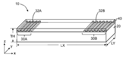
도 1은 본 개시에 따른 예시적인 도파관 기반 AR 광학 시스템 ( "AR 광학 시스템") (10)의 개략적 정면도인 반면, 도 2는 도 1의 예시적인 AR 광학 시스템의 단면도이다. AR 광학 시스템은 도 1에 가장 잘 도시된 바와 같이 x 방향으로 길이 (LZ), y 방향으로 길이 (LY) 및 z 방향으로 전체 두께 (TH)를 가진다.1 is a schematic front view of an exemplary waveguide based AR optical system (“AR Optical System”) 10 according to the present disclosure, while FIG. 2 is a cross-sectional view of the exemplary AR optical system of FIG. 1. The AR optical system has a length (LZ) in the x direction, a length (LY) in the y direction, and a total thickness (TH) in the z direction, as best shown in FIG. 1.
AR 광학 시스템 (10)은 몸체 (21), 상부 표면 (22) 및 하부 표면 (24)을 갖는 기판 (20)을 가진다. 기판 (20)의 몸체 (21)는 굴절률 (nS) 및 두께 (THS)를 가진다. 도시된 예에서, 기판 (20)은 평면이지만, 다른 비-평면 구성도 후술되는 바와 같이 사용될 수 있다.The AR
기판의 상부 표면 (22)은 제 1 격자 요소 (32A)로 구성된 제 1 격자 (30A) 및 격자 요소 (32B)로 구성된 제 2 격자 (30B)를 포함한다. 제 1 및 제 2 격자는 간격 (거리) (SG)에 의해 x 방향으로 이격된다. 제 1 격자 (30A)는 여기에서 "입력" 또는 "입구 동공 (entrance pupil)" 격자로 지칭되는 반면, 제 2 격자 (30B)는 여기에서 "출력" 또는 "출구 동공" 격자로 지칭된다. 입력 및 출력 격자 (30A 및 30B) 각각은 동일한 주기 (Λ) 및 격자 높이 (h)를 가진다.The
일 예에서, 제 1 및 제 2 격자 요소 (32A 및 32B) 중 하나 또는 둘 다는 기판에 형성되어 제 1 및 제 2 격자 요소가 기판 재료로 만들어진다. 이는 마스킹 공정, 에칭 공정, 복제 공정 또는 몰딩 공정을 사용하여 달성될 수 있다. 또 다른 예에서, 제 1 및 제 2 격자 요소 (32A 및 32B) 중 하나 또는 둘 다는 예를 들어 선택적 증착 공정 또는 복제 공정을 통해 기판의 상부 표면에 추가된다. 증착 또는 복제된 제 1 및/또는 제 2 격자 요소 (32A 및 32B)는 기판 (20)과 실질적으로 동일한 굴절률을 갖는 다양한 재료, 예를 들어 무기 재료, 그 예로 산화물 또는 유기 재료 그 예로 아크릴레이트로 구성될 수 있다. 하기에서 논의되는 바와 같이, 입력 및 출력 격자 (30A 및 30B)는 하기에서 더 상세하게 기술된 바와 같이, AR 광학 시스템 (10)으로부터 입력 및 출력되는 광에 대해 위상 정합을 제공한다.In one example, one or both of the first and second
AR 광학 시스템 (10)은 또한 기판 (20)의 상부 표면 (22) 상에 바로 존재하는 도파관 층 (40)을 포함한다. 도파관 층 (40)은 몸체 (41), 상부 표면 (42) 및 하부 표면 (44)을 가지며, 상기 하부 표면은 기판 (20)의 상부 표면 (22)과 인터페이싱된다 (즉, 접촉된다). 이로써, 몸체 (41)의 제 1 부분은 제 1 격자 요소들 (32A) 사이의 공간을 채우면서, 상기 몸체의 제 2 부분은 제 2 격자 요소들 (32B) 사이의 공간을 채운다. 도파관 층 (40)은 굴절률 (nG)를 가지며, 여기서 nG > nS이다. 도파관 층 (40)은 두께 (THG)를 가진다.AR
AR 광학 시스템 (10)의 예시적인 구성에서, 도파관 층 (40)의 상부 표면 (42)은 일 예에서 굴절률 (![]()
![]()
기판 (20), 도파관 층 (40) 및 옵션의 캡 층 (50) 또는 주변 환경 (60)은 도파관 구조체 (100)를 정의하며, 여기서 광은 이하에서 더 상세하게 기술된 바와 같이, 상이한 안내 모드에서 이동하는 안내 파로서 도파관 층 내에서 전파할 수 있다.
AR 광학 시스템 (10)은 기판 (20)의 하부 표면 (24)에 바로 인접한 정면 영역 (FR)을 가진다. AR 광학 시스템 (10)은 또한 캡 층 (50)이 AR 광학 시스템에 사용되는지 여부에 따라서, 도파관 층 (40)의 상부 표면 (42) 또는 캡 층 (50)의 상부 표면 (52)에 바로 인접한 후면 영역 (BR)을 가진다.The AR
일 예에서, 기판 굴절률 (즉, 기판의 몸체 (21)의 굴절률) nS ≤ 1.5이다. 일 예에서, 기판 (20)은 용융 실리카 (fused silica)와 같은 종래의 유리로 제조될 수 있다. 다른 예에서, 기판 (20)은 플라스틱 또는 중합체로 제조될 수 있다. 일 예에서, 기판 (20)은 열가소성 플라스틱로 제조될 수 있다.In one example, the refractive index of the substrate (ie, the refractive index of the
또한, 일 예에서, 도파관 층 굴절률 nG ≥ 2이다. 일 예에서, nG - nS ≥ 0.5이다. 도파관 층 (40)은 또한 적어도 하나의 산화물, 또는 하나 이상의 산화물 재료 및 하나 이상의 플루오라이드 (fluoride) 재료의 조합으로 이루어질 수 있다. 도파관 층 (40)을 위한 예시적인 산화물 재료는 Ta2O5 및 TiO2와 같은 박막을 포함한다.Further, in one example, the waveguide layer refractive index n G ≧2. In one example, n G -n S ≥ 0.5. The
도 4는 도 3과 유사하고, 도파관 구조체 (100)가 굴절률 (nL < nS) 및 두께 (THL)를 가진 저-굴절률 층 (20L)을 포함하는 예시적인 구성을 도시한다. 저-굴절률 층 (20L)은 도파관 층 (40)의 하부 표면 (44)에 바로 인접하여 위치한다. 저-굴절률 층 (20L)은 상부 표면 (22) 상에서 기판 (20)에 추가될 수 있거나, 또는 상부 표면에 형성될 수 있으며, 입력 및 출력 격자 (30A 및 30B)를 포함하거나 지지하는 새로운 기판 상부 표면 (22')을 정의하기 위해 고려될 수 있다. 일 예에서, 저-굴절률 층 (20L)은 굴절률 (nL = 1.38)을 가진 MgF2와 같은 저-굴절률 박막으로 형성된다.4 is similar to FIG. 3 and shows an exemplary configuration in which the
도파관 구조체Waveguide structure
상기에서 유의한 바와 같이, 도파관 구조체 (100)는 주변 환경 (60) 또는 상부 표면 (42)에서의 캡 층 (50) 및 기판 (20) 또는 하부 표면 (44)에서의 저-굴절률 층 (20L)의 비교적 낮은 굴절률로 둘러싸인 비교적 높은 굴절률 도파관 층 (40)에 의해 정의된다. 도파관 구조체 (100)의 도파관 속성은 주로 굴절률 (nG, nS (또는 nL) 및 nA (또는 nC)) 뿐만 아니라, 도파관 층 (40)의 두께 (THG) 및 사용된 광의 동작 파장 (λ)에 의해 정의된다.As noted above, the
비-제한적인 예에서, 도파관 층 (40)의 두께 (THG)는 1 μm ≤ THG ≤ 100 μm의 범위 또는 20 μm ≤ THG ≤ 50 μm의 범위에 있다. 도파관 층 (40)의 정확한 두께 (THG)는 기판 굴절률 (nS) (또는 사용된다면 저-굴절률 층 (20L)의 nL의 굴절률) 및 캡 층 (50)의 굴절률 (nC)에 의존하거나 굴절률 (nA)을 갖는 주변 환경이 사용되는 여부에 의존한다.In a non-limiting example, the thickness (THG) of the
도 5는 도파관 구조체 (100)의 일부의 개략도이다. 도파관 구조체 (100)는, 도파관 구조체가, 기하학적인 광학기의 규칙보다는 오히려 파 전파 (wave propagation)의 전자기 이론에 의해 적절하게 기술된 안내 모드를 지원하다는 점에서 광 가이드 또는 광 파이프로 기술 분야에서 종종 지칭되는 것과는 상이하다. 상기에서 유의한 바와 같이, 일 예에서, 도파관 층 (40)의 전체 도파관 두께 (THG)는, 예를 들어 250 μm 내지 1000 μm의 두께를 가진 종래의 광 가이드에 비해 비교적 얇은 1 ≤ THG ≤ 100 μm의 범위에 있을 수 있다. 일 예에서, 도파관 두께 (THG)는 종래의 광-가이드-기반 AR 광학 시스템에 사용되는 종래의 광 가이드보다 적어도 2.5 배 얇다.5 is a schematic view of a portion of the
도 5는 도파관 층 (40)에서 주로 전파되는 안내 파 또는 안내 모드 (120)를 포함하고, 안내 모드의 테일 (tail) (방출) 부분은 인접한 층에 이동된다. 일 예에서, 도파관 구조체 (100)는 n = 0, 1, 2,… m 개의 안내 모드 (120)를 지원하며, 여기서 n은 모드 번호이고 m은 가장 높은 모드 번호이다. 주어진 편광, 즉 TE 또는 TM에 대한 총 모드 수는 N = m+1이다. n = 0 모드는 기본 모드 (fundamental mode)이고, n > 0 모드는 고차 모드이다. 도 5는 주어진 편광에 대해 도파관 구조체 (100)에 의해 지지되는 총 N = 9 안내 모드 (120)를 나타내는 m = 8인 예를 도시한다.5 includes a guide wave or guide
도파관 구조체 (100)의 예에서, 안내 모드 (120)의 총 수 N은 500 ≤ N ≤ 1000의 범위에 있을 수 있다. 총 모드 수 N은, 충분한 각도 해상도 및 충분히 큰 시야 (FOV) 및 출력 격자 (30B)에 의해 출력된 출력 광 (150')에 대해 실질적으로 연속적인 광 추출을 제공하기에 충분히 크면서 도파관 층 (40)의 두께 (THG)가 비교적 작게, 예를 들어, 100 μm 이하로 유지되도록 선택된다. 예를 들어, FOV는 70˚까지 높을 수 있으며, 더 큰 FOV는 더 많은 수 N의 안내 모드를 필요로 한다. 마찬가지로, 더 작은 FOV는 더 적은 안내 모드 (120)를 필요로 한다. AR 광학 시스템 (10)은 물론 선택된 경우 (예를 들어, 비교적 좁은 시야가 허용되는 경우) 단지 몇 개의 모드 또는 수십 개의 모드로 동작될 수 있지만, AR 광학 시스템이 비교적 큰 FOV를 가지기 위해 수백 개의 모드를 가지는 것이 가장 유용할 것으로 예상된다.In the example of
AR 광학 시스템 파라미터 예AR Optical System Parameter Example
예시적인 AR 광학 시스템 (10)은, 기판 굴절률 nS ![]()
![]()
상기의 것과 유사하지만 도파관 층 (40)이 Nb2O5로 만들어지고 도파관 굴절률 nG = 2.38을 가진 또 다른 예에서, 도파관 구조체 (100)는 약 N = 700 개의 모드를 지원한다.Similar to the above, but in another example where
상기의 것과 유사하지만 도파관 층 (40)이 TiO2로 만들어지고 굴절률 nG = 2.68을 가진 또 다른 예에서, 도파관 구조체 (100)는 약 N = 850 개의 모드를 지원한다.Similar to the above, but in another example where
상기의 것과 유사하지만 기판 (20)이 MgF2로 만들어지고 굴절률 nL = 1.38을 가진 저-굴절률 층 (20L)을 지지하며, 도파관 층 (40)이 굴절률 nG = 2.68을 가진 TiO2로 만들어진 또 다른 예에서, 도파관 구조체 (100)는 약 N = 890 개의 모드를 지원한다.Similar to the above but the
예시에서, 모드 수는 다음 식을 사용하여 계산된다:In the example, the mode number is calculated using the following equation:
![]()
![]()
또한, 일 예에서, 입력 및 출력 격자 (30A 및 30B) 각각은 다음 파라미터를 가질 수 있다: 200 nm 내지 600 nm 범위의 격자 주기 (또는 피치) (Λ) 및 50 nm 내지 500 nm 범위의 격자 요소 높이 (h).Further, in one example, each of the input and
입력 및 출력 격자Input and output grid
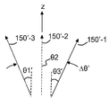
도 6a는 도 2와 유사하고 AR 광학 시스템 (10)의 동작의 기본 원리를 도시한다. 도 6a에서, 입력 광 (150)은 AR 광학 시스템 (10)의 후면 영역 (BR)으로부터 입력 격자 (30A) 상에 입사된다. 하기에서 논의된 바와 같이, 입력 광 (150)은 디스플레이 이미지를 형성하는 디스플레이에 의해 발생될 수 있다. 3 개의 상이한 광선 (150)은 150-1, 150-2 및 150-3으로 표시되고, 일 예에서 z 축에 대해 측정될 수 있는 상이한 입사 각도 (θ)에 대응한다. 여기서, 광선 (150-1, 150-2 및 150-3)은 광파의 전파 방향으로 생각할 수 있다. 도 6b는 입력 광 (150)의 확대도이며, 각도 범위 (Δθ) 내의 3 개의 상이한 예시적인 각도 (θ1, θ2 및 θ3)를 도시한다. 입력 광 (150-1, 150-2 및 150-3)은 후면 영역 (BR)으로부터 입력 격자 (30A)를 향해 일반적으로 -z 방향으로 이동된다.FIG. 6A is similar to FIG. 2 and shows the basic principle of operation of the AR
상이한 각도의 입력 광 (150-1, 150-2 및 150-3)이 입사되어 입력 격자 (30A)와 상호 작용하고, 상기 입력 격자는 입력 광을, 도파관 모드, 입력 격자 및 상이한 입사 각 (θ1, θ2 및 θ3)에서의 입력 광 사이의 위상 정합을 이용하여, 대응하는 상이한 도파관 모드 (120-1, 120-2 및 120-3)로 변환시킨다. 도파관 구조체 (100)가 제한된 수의 안내 모드 (120)를 지원하기 때문에, 입력 각도 범위 내의 선택 입사각 (θ)에서 입력 광 (150)만 안내 모드 (120)로서 도파관 층 (40)에 커플링되어 이동될 것이다. 이들 각도 (θ)는 커플링 각도로 지칭된다. 도파관 구조체 (100)에 의해 지지되는 안내 모드 (120)의 수가 많을수록 커플링 각도 (θ)의 수도 많아진다. 도 6a에서, 설명의 편의를 위해 3 개의 입사 (커플 링) 각도 (θ1, θ2 및 θ3) 만이 도시된다. 상기에서 유의한 바와 같이, 입력 각도 범위 (Δθ)에 의해 정의된 입사 FOV가 1000 개의 커플링 각도 (θ)를 가질 수 있도록 N = 1000 개의 상이한 안내 모드 (120)를 가질 수 있다.Different angles of input light (150-1, 150-2 and 150-3) are incident to interact with the input grating (30A), the input grating providing input light, waveguide mode, input grating and different angles of incidence (θ1 , θ2 and θ3) are converted to the corresponding different waveguide modes 120-1, 120-2 and 120-3 using the phase matching between the input light. Since the
도파관 모드 (120-1, 120-2 및 120-3)는 도파관 구조체 (100) 내에서 출력 격자 (30B)로 이동된다. 입력 및 출력 격자 (30A 및 30B) 위상은 도파관 모드 (120)를 입력 광 및 출력 광 (150 및 150')에 각각 매칭시킨다. 이로써, 도파관 모드 (120-1, 120-2 및 120-3)는, 출력 광 (150')에 대해 출력 각도 범위 △θ' = △θ 내에서 출력 각도 (θ1, θ2 및 θ3)로 방출되는 대응하는 출력 광 (150'-1, 150'-2 및 150'-3)으로서 출력 격자 (30B)에 의해 도파관 층 (40) 외부에 커플링된다. 도 6c는 출력 광 (150')의 확대도이며, 각도 범위 (△θ') 내의 3 개의 상이한 예의 출력 각도 (θ1', θ2' 및 θ3')를 도시한다. 상기에서 유의한 바와 같이, N = 1000 인 경우, 100 개의 상이한 출력 각도 (θ')가 있을 수 있다.The waveguide modes 120-1, 120-2 and 120-3 are moved within the
일 예에서, 입력 및 출력 격자 (30A 및 30B)가 동일한 주기 (Λ)를 가질 때, θ1 = θ1', θ2 = θ2', θ3 = θ3' 및 △θ = △θ' (즉, 커플링 각도는 대응하는 출력 각도와 동일하고 입력 FOV는 출력 FOV와 동일하다). 출력 광 (150')은 일반적으로 +z 방향을 향해 AR 광학 시스템 (10)의 후면 영역 (BR)으로 다시 이동된다. 유의하는 바와 같이, 출력 광 (150')은 일반적으로 입력 광 (150)으로부터의 거리 (SG)만큼 측 방향으로 (도 6a에서 x 방향으로) 변위된다.In one example, when the input and
일 예에서, 입력 광 (150)은 다색성이며, 즉 파장 대역 (Δλ)을 가진다. 예시적인 파장 대역 (Δλ)은 가시 전자기 스펙트럼의 적어도 일 부분을 포함하거나, 상기 부분으로 구성된다.In one example, the
입력 광 (150)이 다색성인 경우, 파장 대역 (Δλ) 내의 각각의 파장 (λ)은 입력 각도 범위 (Δθ)에 걸쳐 대응하는 안내 모드 (120)로서 도파관 구조 (100)에 커플링될 것이다. 상이한 파장의 안내 모드 (120)는 파장 분할 다중화 (WDM) 적용을 위한 안내 모드로서 광 섬유에서 상이한 파장의 광이 전파되는 것과 동일한 방식으로 도파관 구조체 내에서 독립적으로 전파된다. 입력 및 출력 격자 (30A 및 30B)에 의해 제공된 위상 정합으로 인해, 출력 광 (150')의 스펙트럼 함량 및 분포는 입력 광 (150)과 동일 (또는 적어도 실질적으로 동일)하다. 이로써, AR 광학 시스템 (10)은 컬러 이미징이 가능하다.When the
한편, 일 예에서, 상이한 광 (250) (예를 들어, 도시되지 않은 객체 또는 장면으로부터의 가시 광)은 AR 광학 시스템 (10)을 통해 정면 영역 (FR)으로부터 후면 영역 (BR)으로 이동되고, 특히 격자 요소 (32B)에 수직인 방향으로, 즉 +z 방향으로 출력 격자 (30B)를 통과한다. 광 (250)이 통과함에 따라 상기 광은 출력 격자 (30B)에 의해 실질적으로 왜곡되지 않는다. 이는 출력 격자 (30B)에 의해 광 (250)에 제공되는 위상 정합이 없기 때문이다.Meanwhile, in one example, different lights 250 (eg, visible light from an object or scene not shown) are moved from the front area FR to the back area BR through the AR
AR 광학 시스템 (10)에서 도파관 구조체 (100)를 이용하는 이점은 출력 광 (150)이 출력 격자 (30B)의 길이를 따라 실질적으로 연속적으로 방출된다는 점이다. 이는, 광선이 전 반사에 의해 광 가이드 내에 갇히고 광 가이드를 따라 별개의 위치에서만 나오는 종래의 광-안내-기반 AR 시스템과 대조적이다. 종래의 광 가이드에 대한 별개의 추출과는 달리, 출력 격자 (30B)를 따라 출력 광 (150')의 연속 추출은 출력 격자 (즉, 출구 동공)에 걸쳐 보다 균일한 광 분포를 초래하여, 이로써 사용자에 의해 관찰되는 바와 같이 해당하는 더 우수한 증강 이미지 품질을 만들어낸다.The advantage of using the
일 예에서, 입력 광 (150)은 또한 단색성 이미징을 위해 실질적으로 단색성일 수 있다. 또한 일 예에서, AR 광학 시스템 (10)은 입력 광 (150)의 상이한 선택 파장을 개별적으로 핸들링하도록 구성될 수 있다. 예를 들어, 적색 (R), 녹색 (G) 및 청색 (B) 성분을 가진 입력 광 (150)의 경우, 3 개의 상이한 도파관 구조체 (100)는 적층된 구성으로 배치될 수 있고 간격 층 (예를 들어, 공기 또는 저-굴절률 필름)을 사용하여 분리될 수 있고, 이때 상이한 도파관 구조체 각각은 R, G 및 B 입력 광 (150)을 핸들링하도록 구성된다. 또 다른 예에서, 두 개의 도파관 구조체 (100)는 적층될 수 있으며, 하나의 도파관 구조체는 R 및 G 입력 광 (150)을 핸들링하도록 설계되는 반면, 다른 도파관 구조체는 G 및 B 입력 광을 핸들링하도록 설계된다. 이로써, AR 광학 시스템 (10)에 대한 적층 구성은 비-적층 구성과 본질적으로 동일한 방식으로 동작하며, 입력 광 (150)의 상이한 파장은 상이한 도파관 구조체에서 이동된다.In one example, the
격자 구성 예Grid configuration example
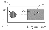
도 7a 내지 7d는 입력 격자 (30A) 및 출력 격자 (30B)에 대한 예시적인 구성을 도시하는 AR 광학 시스템 (10)을 위에서 아래로 본 도면 예이다. 도 7a 및 7b의 예에서, 입력 격자 (30A)는 선형 격자 요소 (32A) 및 전체 원형 형상을 가지는 반면, 출력 격자 (30B)도 선형 격자 요소 (32B)를 가지지만 전체 직사각형 형상을 가진다. 게다가, 이 예에서, 입력 격자 (30A)는 출력 격자 (30B)보다 실질적으로 작은 면적을 가진다.7A-7D are examples of views from top to bottom of the AR
도 7a의 출력 격자 (30B)는 x-축과 평행한 전파 벡터 K로 도시된 반면, 도 7b의 출력 격자는 각도 (θ)로 정의된 바와 같이 x-y 평면에서 전파 벡터를 가진다.The output grating 30B of FIG. 7A is shown as a propagation vector K parallel to the x-axis, while the output grating of FIG. 7B has a propagation vector in the x-y plane as defined by the angle θ.
도 7c는 출력 격자 (30B)가 θ1에 의해 정의된 K1 및 θ2에 의해 정의된 K2인 적어도 2 개의 격자 운동량 벡터를 정의하는 교차 요소 (32A 및 32B)를 갖는 2 차원 구성을 가진 일 예를 도시한다. 출력 격자는 각도 (θi)로 정의된 추가 격자 전파 (운동량) 벡터 (Ki)를 가질 수 있다.Figure 7c with a two-dimensional configuration with an output grid (30B) has a K 1 and the cross elements (32A and 32B) that defines the K 2 is at least two gratings momentum vector defined by θ 2 defined by θ 1 An example is shown. The output grating can have an additional grating propagation (momentum) vector (K i ) defined by the angle (θ i ).
다른 예에서, 출력 격자 (30B)는 도 7d에 도시된 바와 같은 곡선 격자 요소 (32B)를 포함할 수 있고, 격자 요소는 연속체 전파 벡터 (K)를 정의하도록 동심으로 배치된다.In another example, the output grating 30B can include a curved
AR 광학 시스템 (10)의 원하는 기능에 따라, 입력 및 출력 격자 (30A 및 30B)의 격자 요소 (32A 및 32B)에 대한 다양한 형상 및 크기가 효과적으로 사용될 수 있다. 부가적으로, 입력 및/또는 출력 격자 (30A 및/또는 30B)는 상이한 타입의 격자 요소 (32A 및/또는 32B)를 갖는 2 개 이상의 별개의 격자 영역을 포함할 수 있다. 입력 격자 (30A) 및/또는 출력 격자 (30B)에 대한 2 차원 구성은 AR 광학 시스템 (10)의 전체 면적을 감소시키고 격자 레이아웃을 단순화하는 것이 바람직한 경우에 효과적으로 사용될 수 있다.Depending on the desired function of the AR
곡선 AR 광학 시스템Curved AR optical system
상술된 AR 광학 시스템 (10)은 예시 및 도시와 설명의 용이성을 위해 평면 구성을 가진다. 그러나, AR 광학 시스템 (10)은 이에 제한되지 않고 곡선화될 수 있으며, 즉, 하나 이상의 곡선 표면을 가질 수 있다.The AR
도 8은 도 2와 유사하고 볼록 곡률을 2 개의 표면을 가진 AR 광학 시스템 (10)의 실시예를 도시한다. 도 9는 도 8과 유사하고 오목 곡률을 갖는 2 개의 표면을 가진 AR 광학 시스템 (10)의 실시예를 도시한다. 다른 예는 도 10에 도시된 바와 같이 최하부 표면과 같이 곡선화된 AR 광학 시스템 (10)의 단 하나의 표면을 포함할 수 있다. 도 11은 AR 광학 시스템 (10)이 캡 층 (50)을 포함하고 캡 층의 상부 표면 (52)이 곡선화되면서 도파관 층 (40)이 실질적으로 평면으로 된 일 예를 도시한다.FIG. 8 shows an embodiment of an AR
일 예에서, 하나 이상의 곡선 표면은 교정 이미징을 제공하도록 구성될 수 있다. 도 12는 기판 (20)의 하부 표면 (24)이 사용자 (350)에 대한 교정 이미징을 제공하도록 설계된 국부적으로 곡선화된 부분 (24C)을 포함하는 예시적인 실시예를 도시한다 (이하에서 도입 및 논의되는 도 13a 참조).In one example, one or more curved surfaces can be configured to provide corrective imaging. 12 shows an exemplary embodiment in which the
부가적으로, AR 광학 시스템 (10)은 기판 (20)의 하부 표면 (24) 상에 위치된 도파관 층 (40)으로 구성될 수 있으며, 여기에 개시된 예시적인 구성은 도시를 위해 기판의 상부 표면 상에 도파관 층을 나타낸다. 부가적으로, AR 광학 시스템 (10) 내의 임의의 표면 (또는 그 일 부분)은 교정 표면으로서 구성될 수 있다. 예에서, AR 광학 시스템 (10)은 다수의 교정 표면을 가질 수 있다. 마찬가지로, 다양한 곡률 조합 (예를 들어, 볼록 및 오목)은 도 8 내지 12의 도시에 의해 나타난 예를 넘어서 사용될 수 있다.Additionally, the AR
AR 광학 시스템 (10)의 도파관 구조체 (100)가 비교적 강한 곡률을 가진 구성에서, 안내 모드 (120)는 더 이상 실제 경계 모드 (true bound modes)가 아닐 수 있지만, 누설 공진 모드로서 보다 적절하게 기술된다. 누설 공진 모드는 도파관 구조체 (100)의 동작을 실질적으로 변화시키지 않으며, 실제로, 입력 (커플 링) 각도 (θ)의 범위를 각 모드에 커플링하고 각 모드에 대한 별개의 커플링 각도와 반대로 함으로써 각도 해상도를 개선시킬 수 있다.In a configuration in which the
다른 예에서, 입력 및 출력 격자 (30A 및 30B)의 격자 주기 (L)는 도파관 구조체 (100)에서의 임의의 곡률을 처리하고 입사 광 (150)에 대한 정확한 결커플링 각도 (θ)를 유지하고, 이뿐 아니라 출력 광 (150')에 대한 출력 각도 (θ')를 유지하기 위해 일정하지 않을 수 있다 (예를 들어, 처프될 수 있다 (chirped)). 입력 및 출력 격자의 격자 높이 (h)는 도파관 구조체 (100)에 입력 광 (150)이 커플링되고 도파관 구조체 외부에서는 출력 광 (150')이 각각 커플링되는 속도를 변화시키기 위해 일정하지 않을 수 있다.In another example, the grating period (L) of the input and
AR 시스템AR system
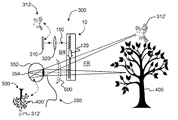
도 13a는 여기에 개시된 AR 광학 시스템 (10)을 포함하는 AR 시스템 (300)의 예시적인 실시예의 개략도이다. AR 광학 시스템 (10)의 평면 구성은 예로서 그리고 설명의 편의를 위해 도시된다. AR 시스템 (300)은 커플링 광학 시스템 (320)에 의해 AR 광학 시스템 (10)의 입력 격자 (30A)에 광학적으로 커플링된 디스플레이 장치 (310)를 포함한다. 일 예에서, 디스플레이 장치 (300)는 마이크로 디스플레이, 예를 들어 마이크로 디스플레이 칩이다. 일 예에서, 커플링 광학 시스템 (320)은 렌즈, 미러, 빔 스플리터 등과 같은 하나 이상의 광학 요소를 포함한다. 커플링 광학 시스템 (320)은 크기 및 무게를 최소화하기 위해 마이크로 광학 요소를 포함할 수 있다.13A is a schematic diagram of an exemplary embodiment of an
AR 시스템 (300)은 사용자 (350)에 대해 그리고 실제 객체 (400)에 대해 배치된 것으로 도시되고, 상기 실제 객체는 AR 광학 시스템 (10)의 정면 영역 (FR)에 인접하여 존재하고 예를 들어 나무로 도시된다. 실제 객체 (400)는 또한 AR 광학 시스템 (10)을 통해 사용자가 보고 있는 장면으로 간주될 수 있다. 디스플레이 장치 (310)는 디스플레이 이미지 (312)를 제공하는 것으로 도시되며, 상기 이미지는 예를 들어 조류로 도시된다. 디스플레이 이미지 (312)와 연관된 디스플레이 광을 구성하는 광 (150)은 커플링 광학 시스템 (320)에 의해 입력 (커플링) 각도 (θ) 범위 (△θ)에 걸쳐 (예를 들어, 입력 FOV에 걸쳐) AR 광학 시스템 (10)의 입력 격자 (30A)에 지향된다. 입력 (디스플레이) 광 (150)은, 상술한 바와 같이, 입력 (FOV) 내의 선택 커플링 각도 (θ)에서 도파관 구조체 (100)에 광학적으로 커플링되어 다수의 (N) 안내 모드 (120)를 발생시킨다. N 안내 모드 (120)는 그 후 도파관 구조체 (100) 내에서 출력 격자 (30B)로 이동하고, 위상 정합을 제공하는 입력 및 출력 격자 (30A 및 30B)는 N 개의 안내 모드 (120)를, 안내 모드 (120)의 개수 (N)에 대응하는 별개의 출력 각도 (θ')에서 대응하는 출력 광 (150')으로 변화시킨다. 출력 각도 (θ')가 별개이자만, 출력 광 (150')은 출력 격자 (30B)의 길이에 걸쳐 실질적으로 연속적으로 아웃 커플링된다.The
출력 광 (150 ')은 사용자 (350)의 하나 또는 양쪽 눈 (352)으로 지향된다. 마찬가지로, 사용자의 하나 또는 양쪽 눈은 출력 격자 (30B)를 통해 객체 (400)로부터 직접 광 (250)을 수신한다 (또한, 도 6a 참조). 이로써, 사용자 (350)의 눈 또는 눈들 (352)은 눈의 망막 (354) 상에 증강 이미지 (500)를 형성하며, 증강 이미지는 객체 (400)의 실제 이미지 (400') 및 디스플레이 이미지 (312)의 가상 이미지 (312')를 포함한다.The output light 150' is directed to one or both
일 예에서, AR 시스템 (300)은, 예를 들어, 사용자의 눈이 수차를 갖는 경우에, 교정 이미징을 제공하기 위해 사용자 (350)의 눈 (352)과 AR 광학 시스템 (10) 사이에 동작 가능하게 배치된 적어도 하나의 교정 렌즈 (600)를 옵션으로 포함할 수 있다. 일 예에서, 교정 렌즈 (600)는 하나 이상의 종래의 안경 렌즈를 구성한다. 상기에서 유의한 바와 같이, 교정 이미징은 또한 곡선화된 표면 도파관 구조체 (100) 중 하나 이상의 적어도 일 부분에 의해 제공될 수 있다.In one example,
도 13b는 여기에 개시된 AR 시스템 (10)을 포함하고 사용자 (350)가 착용할 수 있는 예시적인 AR 아이웨어 (650)의 개략도이다. AR 아이웨어는 렌즈 (652) 및 템플 (temples, 654)을 포함한다. 도시된 예에서, 각각의 렌즈 (352)는 출력 격자 (30B)를 포함한다. 입력 격자 (30A)는 렌즈 (352)의 각각의 외부 부분에 위치한다. 각각의 렌즈 (352)의 적어도 일 부분은 상술된 도파관 구조체 (100)를 포함한다. 디스플레이 장치 (예를 들어, 마이크로-디스플레이) (310) 및 커플링 광학 시스템 (320)은 템플 (654) 각각에 의해 지지될 수 있다 (하나의 디스플레이 및 커플링 광학 시스템만이 도시를 용이하게 하기 위해 도시됨).13B is a schematic diagram of an
도 14는 도 13a와 유사하고 사용자 (350)가 이미징 광학 시스템 (700)으로 교체되는, 즉 이미징 광학 시스템이 사용자의 눈 (352)을 대체하는 AR 시스템 (300)의 예시적인 실시예를 도시한다. 이미징 광학 시스템 (700)은 이미징 렌즈 (702) 및 이미지 센서 (704)를 포함하며, 상기 이미지 센서 상에는 증강 이미지 (500)가 형성된다. 일 예에서, 이미징 광학 시스템 (700)은 디지털 카메라를 포함한다. 일 예에서, 이미지 센서 (704)는 예를 들어 디지털 카메라에 연관된 바와 같은 이미지 프로세싱 전자기기 (710)에 동작 가능하게 결합된다. 일 예에서, 사용자의 눈 (352)은 이미징 광학 시스템 (700)의 예를 구성하며, 사용자의 뇌는 증강 이미지 (500)의 필요한 이미지 프로세싱을 수행한다.FIG. 14 is similar to FIG. 13A and shows an exemplary embodiment of
첨부된 청구 범위에 정의된 바와 같은 본 개시의 기술 사상 또는 권리 범위를 벗어나지 않으면서 여기에 기술된 바와 같은 본 개시의 바람직한 실시 예에 대한 다양한 수정이 이루어질 수 있는 것은 통상의 기술자에게 명백할 것이다. 이로써, 본 개시는 수정 및 변형을 포함하되, 수정 및 변형이 첨부된 청구 범위 및 그 등가물의 범위 내에 있는 경우에 그러하다.It will be apparent to those skilled in the art that various modifications may be made to the preferred embodiments of the present disclosure as described herein without departing from the spirit or scope of the present disclosure as defined in the appended claims. As such, the present disclosure includes modifications and variations, where such modifications and variations are within the scope of the appended claims and their equivalents.
Claims (34)
상기 동작 파장에서의 굴절률 (nS), 상부 표면 및 하부 표면을 가지는 기판;
상기 기판의 상부 표면에 또는 상기 상부 표면 상에 각각 형성되고 서로 측 방향으로 이격된 입력 격자 및 출력 격자;
몸체, 상부 표면, 하부 표면 및 1 μm ≤ THG ≤ 100 μm인 두께 (THG)를 가진 도파관 층, 여기서 상기 도파관 층의 하부 표면은 상기 기판의 상부 표면 상에 지지되어 상기 입력 및 출력 격자는 상기 도파관 층으로 연장되고 상기 도파관 층은 상기 동작 파장에서 굴절률 (nS) 이상인 굴절률 (nG) (nG ≥ nS)을 가지고, 다수의 안내 모드를 지원함;을 포함하며,
상기 입력 및 출력 격자는, 상기 입력 격자 상에 입사된 입력 광이 상기 도파관 층에 커플링되고 상기 안내 모드에서 상기 출력 격자로 이동되며, 그리고 출력 광으로서 상기 출력 격자에 의해 상기 도파관 층 외부에서 커플링되도록, 위상 정합을 제공하는, 증강 현실 광학 시스템.An augmented reality optical system for use in an augmented reality system at an operating wavelength, comprising:
A substrate having a refractive index (n S ) at the operating wavelength, an upper surface and a lower surface;
An input grating and an output grating respectively formed on or on the upper surface of the substrate and spaced laterally from each other;
Body, top surface, bottom surface and a waveguide layer having a thickness (THG) of 1 μm ≤ THG ≤ 100 μm, wherein the bottom surface of the waveguide layer is supported on the top surface of the substrate such that the input and output gratings are the waveguide Includes a layer that extends into the layer and the waveguide layer has a refractive index (n G ) (n G ≥ n S ) that is greater than or equal to the refractive index (n S ) at the operating wavelength, and supports multiple guide modes;
In the input and output gratings, input light incident on the input grating is coupled to the waveguide layer and moved to the output grating in the guided mode, and coupled outside the waveguide layer by the output grating as output light. An augmented reality optical system that provides phase matching, so as to be ringed.
상기 동작 파장에서, 상기 기판의 굴절률 (nS)은 1.5 이하이고 (nS ≤ 1.5), 상기 도파관 층 굴절률 (nG)은 2 이상인 (nG ≥ 2), 증강 현실 광학 시스템.The method according to claim 1,
At the operating wavelength, the refractive index (n S ) of the substrate is 1.5 or less (n S ≤ 1.5), and the waveguide layer refractive index (n G ) is 2 or more (n G ≥ 2), and the augmented reality optical system.
다수의 안내 모드 수는 500 내지 1000인, 증강 현실 광학 시스템.The method according to claim 2,
Augmented reality optical system, wherein the number of guide modes is 500 to 1000.
상기 도파관 층은 25 μm ≤ THG ≤ 50 μm 범위의 두께 (THG)를 가지는, 증강 현실 광학 시스템.The method according to claim 1 or 2,
Wherein the waveguide layer has a thickness (THG) in the range of 25 μm ≤ THG ≤ 50 μm.
상기 도파관 층은 30 μm ≤ THG ≤ 40 μm 범위의 두께 (THG)를 가지는, 증강 현실 광학 시스템.The method according to claim 1 or 2,
Wherein the waveguide layer has a thickness (THG) in the range of 30 μm ≤ THG ≤ 40 μm.
상기 도파관 층은 중합체를 포함하고, 상기 기판은 유리를 포함하는, 증강 현실 광학 시스템.The method according to any one of claims 1 to 5,
Wherein the waveguide layer comprises a polymer, and the substrate comprises glass.
상기 기판은 유리 재료를 포함하고, 상기 도파관은 산화물 재료 및 플루오 라이드 재료 중 적어도 하나를 포함하는, 증강 현실 광학 시스템.The method according to any one of claims 1 to 6,
Wherein the substrate comprises a glass material, and the waveguide comprises at least one of an oxide material and a fluoride material.
상기 기판은 유리 재료를 포함하고, 상기 입력 및 출력 격자는 중합체를 포함하고, 상기 도파관 층은 산화물 재료, 또는 산화물 재료와 플루오라이드 재료의 조합을 포함하는, 증강 현실 광학 시스템.The method according to any one of claims 1 to 5,
Wherein the substrate comprises a glass material, the input and output gratings comprise a polymer, and the waveguide layer comprises an oxide material, or a combination of an oxide material and a fluoride material.
상기 기판은 중합체 재료를 포함하고, 상기 도파관 층은 산화물 재료 또는 산화물 재료 및 플루오라이드 재료의 조합을 포함하는, 증강 현실 광학 시스템.The method according to any one of claims 1 to 5,
Wherein the substrate comprises a polymeric material, and the waveguide layer comprises an oxide material or a combination of an oxide material and a fluoride material.
상기 중합체 재료는 열가소성 플라스틱을 포함하는, 증강 현실 광학 시스템.The method according to claim 9,
The polymer material comprises a thermoplastic, augmented reality optical system.
상기 도파관 층은 실리콘을 포함하는, 증강 현실 광학 시스템.The method according to claim 9 or 10,
The waveguide layer comprises silicon, augmented reality optical system.
상기 도파관 층 및 상기 기판 각각은 평면인, 증강 현실 광학 시스템.The method according to any one of claims 1 to 11,
Each of the waveguide layer and the substrate is planar, augmented reality optical system.
상기 도파관 층 및 상기 기판 중 적어도 하나는 곡선 표면을 가지는, 증강 현실 광학 시스템.The method according to any one of claims 1 to 12,
And at least one of the waveguide layer and the substrate has a curved surface.
상기 도파관 층의 상부 표면 상에 배치된 캡 층을 더욱 포함하며, 상기 캡 층은 nG 미만의 굴절률 (nC) (nC < nG)을 가지는, 증강 현실 광학 시스템.The method according to any one of claims 1 to 13,
Wherein further comprising a cap layer disposed on an upper surface of the wave guide layer, the cap layer has a refractive index less than n G (n C) (n C <n G) having a, AR optical system.
상기 입력 격자는 선형 입력 격자 요소를 포함하고, 상기 출력 격자는 선형 출력 격자 요소를 포함하는, 증강 현실 광학 시스템.The method according to any one of claims 1 to 14,
Wherein the input grating comprises a linear input grating element, and the output grating comprises a linear output grating element.
상기 입력 격자는 2 차원 입력 격자 요소를 포함하고, 상기 출력 격자는 2 차원 출력 격자 요소를 포함하는, 증강 현실 광학 시스템.The method according to any one of claims 1 to 15,
Wherein the input grating comprises a two-dimensional input grating element, and the output grating comprises a two-dimensional output grating element.
상기 출력 광은 50˚≤FOV≤70˚ 범위의 시야 (FOV)를 가지는, 증강 현실 광학 시스템.The method according to any one of claims 1 to 16,
The output light has a field of view (FOV) in the range of 50˚≤FOV≤70˚, augmented reality optical system.
상기 입력 광은 다색성인, 증강 현실 광학 시스템.The method according to any one of claims 1 to 17,
The input light is multicolor, augmented reality optical system.
상기 입력 광은 단색성인, 증강 현실 광학 시스템.The method according to any one of claims 1 to 17,
The input light is monochromatic, augmented reality optical system.
상기 기판은 기판 상부 표면을 정의하는 저-굴절률 층을 포함하고, 상기 저-굴절률 층은 nS 미만인 굴절률 (nL) (nL<nS)을 가지는, 증강 현실 광학 시스템.The method according to any one of claims 1 to 19,
The substrate is that which defines the substrate upper surface and including a high refractive index layer, the low-refractive index layer is lower than refractive index n S (n L) (n L < n S) with a, AR optical system.
청구항 1 내지 20 중 어느 한 항에 따르고 정면 영역 및 후면 영역을 가지는 증강 현실 광학 시스템;
상기 후면 영역에 배치되고 입력 광을 발생시키는 디스플레이 장치; 및
상기 디스플레이 장치에 대해 동작 가능하게 배치되고, 입력 시야에 걸쳐 상기 증강 현실 광학 시스템의 입력 격자에 상기 입력 광을 지향시키도록 구성된 커플링 광학 시스템;을 포함하는, 증강 현실 시스템.In the augmented reality system for viewing objects or scenes,
An augmented reality optical system according to claim 1 and having a front area and a back area;
A display device disposed in the rear area and generating input light; And
And a coupling optical system operatively disposed relative to the display device and configured to direct the input light to an input grating of the augmented reality optical system across an input field of view.
출력 시야에 걸쳐 출력 격자로부터 출력 광을 수신하도록 상기 후면 영역에 동작 가능하게 배치된 이미징 광학 시스템을 더욱 포함하는, 증강 현실 시스템.The method of claim 21,
And an imaging optical system operatively disposed in the rear region to receive output light from an output grating over an output field of view.
상기 객체 또는 상기 장면으로부터의 광은 상기 출력 격자를 통해 상기 정면 영역으로부터 상기 후면 영역으로 그리고 상기 이미징 광학 시스템으로 전송되고, 상기 이미징 광학 시스템은 증강된 이미지를 형성하기 위해 상기 객체 또는 상기 장면으로부터의 광 및 상기 출력 광을 조합하는, 증강 현실 시스템.The method according to claim 21 or 22,
Light from the object or the scene is transmitted through the output grating from the front area to the back area and to the imaging optical system, the imaging optical system from the object or the scene to form an augmented image. An augmented reality system that combines light and the output light.
상기 이미징 광학 시스템은 사용자의 적어도 하나의 눈을 포함하는, 증강 현실 시스템.The method according to any one of claims 21 to 23,
The imaging optical system comprises at least one eye of a user, an augmented reality system.
상기 출력 시야는 50˚ 내지 70˚의 범위에 있는, 증강 현실 시스템.The method of claim 21,
The output field of view is in the range of 50˚ to 70˚, augmented reality system.
상기 입력 광은 다색성인, 증강 현실 시스템.The method of claim 21,
The input light is multicolor, augmented reality system.
굴절률 (nG) 및 1 μm ≤ THG ≤ 100 μm 범위의 두께 (THG)를 가진 도파관 층을 포함한 도파관 구조체, 여기서 상기 도파관 구조체는 굴절률 (nS)를 가진 기판 상에 지지되고, nG - nS ≥ 0.5이며, 상기 도파관 구조체는 다수의 안내 모드를 지원함; 및
상기 도파관 층 내에 각각 존재하는 입력 격자 및 출력 격자, 여기서 상기 입력 및 출력 격자는 위상 정합을 제공하고 서로 측 방향으로 이격됨;를 포함하는, 증강 현실 광학 시스템.In the augmented reality optical system,
A waveguide structure comprising a waveguide layer having a refractive index (n G ) and a thickness (THG) in the range of 1 μm ≤ THG ≤ 100 μm, wherein the waveguide structure is supported on a substrate having a refractive index (n S ), n G -n S ≥ 0.5, the waveguide structure supports multiple guide modes; And
And an input grating and an output grating each present in the waveguide layer, wherein the input and output gratings provide phase matching and are spaced laterally from each other.
상기 도파관 층은 중합체 재료를 포함하며, 상기 기판은 유리 재료를 포함하는, 증강 현실 광학 시스템.The method according to claim 27,
Wherein the waveguide layer comprises a polymer material, and the substrate comprises a glass material.
상기 입력 및 출력 격자는 가시 동작 파장 대역에 걸쳐 동작하도록 구성되는, 증강 현실 광학 시스템.The method according to claim 27 or 28,
Wherein the input and output gratings are configured to operate over a visible operating wavelength band.
상기 도파관 층 및 상기 기판 중 적어도 하나는 평면인, 증강 현실 광학 시스템.The method according to any one of claims 27 to 29,
Wherein the at least one of the waveguide layer and the substrate is planar.
도파관 구조체에서 이동하는 다수의 안내 모드를 형성하기 위해 입력 시야에 걸쳐 디스플레이 이미지로부터의 디스플레이 광을 상기 도파관 구조체의 입력 격자로 지향시키는 단계;
상기 도파관 구조체의 출력 격자를 사용하여 출력 시야에 걸쳐 상기 다수의 안내 모드를 아웃 커플링하는 단계, 여기서 상기 출력 격자는 상기 입력 격자와 위상 정합되고 상기 입력 격자로부터 이격되어 있음;
이미징 광학 시스템을 사용하여 상기 출력 격자로부터 출력 광을 수신하는 동안 상기 출력 격자를 통해 상기 이미징 광학 시스템으로 상기 객체 또는 상기 장면을 보는 단계; 및
상기 디스플레이 이미지 및 상기 객체 또는 상기 장면의 이미지가 조합된 증강 이미지를, 상기 이미징 광학 시스템으로 형성하는 단계;를 포함하는, 증강 현실 이미지 형성 방법.A method of forming an augmented reality image when viewing an object or scene,
Directing display light from a display image across an input field of view to an input grating of the waveguide structure to form a number of guide modes moving in the waveguide structure;
Out-coupling the plurality of guide modes over an output field of view using the output grating of the waveguide structure, wherein the output grating is phase-matched with and spaced from the input grating;
Viewing the object or the scene with the imaging optical system through the output grating while receiving output light from the output grating using an imaging optical system; And
And forming an augmented image in which the display image and the image of the object or the scene are combined with the imaging optical system.
상기 출력 시야는 50˚ 내지 70˚ 범위에 있는, 증강 현실 이미지 형성 방법.The method according to claim 31,
The output field of view is in the range of 50˚ to 70˚, augmented reality image forming method.
상기 이미징 광학 시스템은 사용자의 적어도 하나의 눈을 포함하는, 증강 현실 이미지 형성 방법.The method of claim 31 or 32,
Wherein the imaging optical system comprises at least one eye of a user.
상기 도파관 구조체는 증강 현실 아이웨어에 통합되는, 증강 현실 이미지 형성 방법.The method according to any one of claims 31 to 33,
The waveguide structure is integrated in augmented reality eyewear, augmented reality image forming method.
Applications Claiming Priority (3)
| Application Number | Priority Date | Filing Date | Title |
|---|---|---|---|
| US201762572109P | 2017-10-13 | 2017-10-13 | |
| US62/572,109 | 2017-10-13 | ||
| PCT/US2018/055399 WO2019075192A1 (en) | 2017-10-13 | 2018-10-11 | Waveguide-based optical systems and methods for augmented reality systems |
Publications (1)
| Publication Number | Publication Date |
|---|---|
| KR20200069335A true KR20200069335A (en) | 2020-06-16 |
Family
ID=63966162
Family Applications (1)
| Application Number | Title | Priority Date | Filing Date |
|---|---|---|---|
| KR1020207013338A Withdrawn KR20200069335A (en) | 2017-10-13 | 2018-10-11 | Waveguide-based optical system and method for augmented reality system |
Country Status (7)
| Country | Link |
|---|---|
| US (1) | US10929667B2 (en) |
| EP (1) | EP3695269A1 (en) |
| JP (1) | JP7121116B2 (en) |
| KR (1) | KR20200069335A (en) |
| CN (1) | CN111226157B (en) |
| TW (1) | TWI802601B (en) |
| WO (1) | WO2019075192A1 (en) |
Families Citing this family (47)
| Publication number | Priority date | Publication date | Assignee | Title |
|---|---|---|---|---|
| US11726332B2 (en) | 2009-04-27 | 2023-08-15 | Digilens Inc. | Diffractive projection apparatus |
| WO2016020630A2 (en) | 2014-08-08 | 2016-02-11 | Milan Momcilo Popovich | Waveguide laser illuminator incorporating a despeckler |
| EP2842003B1 (en) | 2012-04-25 | 2019-02-27 | Rockwell Collins, Inc. | Holographic wide angle display |
| US9933684B2 (en) | 2012-11-16 | 2018-04-03 | Rockwell Collins, Inc. | Transparent waveguide display providing upper and lower fields of view having a specific light output aperture configuration |
| WO2016042283A1 (en) | 2014-09-19 | 2016-03-24 | Milan Momcilo Popovich | Method and apparatus for generating input images for holographic waveguide displays |
| US10437064B2 (en) | 2015-01-12 | 2019-10-08 | Digilens Inc. | Environmentally isolated waveguide display |
| US9632226B2 (en) | 2015-02-12 | 2017-04-25 | Digilens Inc. | Waveguide grating device |
| WO2017060665A1 (en) | 2015-10-05 | 2017-04-13 | Milan Momcilo Popovich | Waveguide display |
| EP3548939A4 (en) | 2016-12-02 | 2020-11-25 | DigiLens Inc. | WAVE GUIDE DEVICE WITH UNIFORM OUTPUT LIGHTING |
| US10545346B2 (en) | 2017-01-05 | 2020-01-28 | Digilens Inc. | Wearable heads up displays |
| CN114721242B (en) | 2018-01-08 | 2025-08-15 | 迪吉伦斯公司 | Method for manufacturing optical waveguide |
| JP7456929B2 (en) | 2018-01-08 | 2024-03-27 | ディジレンズ インコーポレイテッド | Systems and methods for manufacturing waveguide cells |
| JP7404243B2 (en) | 2018-01-08 | 2023-12-25 | ディジレンズ インコーポレイテッド | Systems and methods for high-throughput recording of holographic gratings in waveguide cells |
| US10877275B2 (en) * | 2018-02-15 | 2020-12-29 | Hitachi, Ltd. | Imageguide for head mounted display |
| WO2020149956A1 (en) | 2019-01-14 | 2020-07-23 | Digilens Inc. | Holographic waveguide display with light control layer |
| US20200247017A1 (en) | 2019-02-05 | 2020-08-06 | Digilens Inc. | Methods for Compensating for Optical Surface Nonuniformity |
| EP3924759B1 (en) | 2019-02-15 | 2025-07-30 | Digilens Inc. | Methods and apparatuses for providing a holographic waveguide display using integrated gratings |
| US20220283377A1 (en) | 2019-02-15 | 2022-09-08 | Digilens Inc. | Wide Angle Waveguide Display |
| CN113811803A (en) * | 2019-03-12 | 2021-12-17 | 奇跃公司 | Waveguide with high refractive index material and method of making the same |
| US11349567B2 (en) | 2019-03-13 | 2022-05-31 | Telefonaktiebolaget Lm Ericsson (Publ) | Use of waveguides and lenses to improve light communication reception in devices |
| US10958340B2 (en) | 2019-05-09 | 2021-03-23 | Telefonaktiebolaget Lm Ericsson (Publ) | Multi-channel light communications via waveguides |
| EP3980825A4 (en) | 2019-06-07 | 2023-05-03 | Digilens Inc. | WAVEGUIDES INCORPORATING TRANSPARENT AND REFLECTIVE GRATINGS AND METHODS OF MAKING THEREOF |
| JP2022546413A (en) | 2019-08-29 | 2022-11-04 | ディジレンズ インコーポレイテッド | Vacuum grating and manufacturing method |
| US10895701B1 (en) * | 2019-09-17 | 2021-01-19 | Telefonaktiebolaget Lm Ericsson (Publ) | Light guide structure with multiple entrances |
| CN112764159B (en) * | 2019-10-21 | 2023-06-16 | 杭州光粒科技有限公司 | Optical waveguide element, method of manufacturing the same, and holographic optical waveguide display device |
| TWI858170B (en) * | 2019-10-23 | 2024-10-11 | 以色列商魯姆斯有限公司 | Displays employing astigmatic optics and aberration compensation |
| US11054566B2 (en) * | 2019-10-25 | 2021-07-06 | Facebook Technologies, Llc | Display waveguide with a high-index layer |
| CN113325506A (en) * | 2020-02-28 | 2021-08-31 | 苏州苏大维格科技集团股份有限公司 | Holographic optical waveguide lens and augmented reality display device |
| CN111812841B (en) * | 2020-03-06 | 2023-07-07 | 谷东科技有限公司 | Volume holographic grating two-dimensional pupil expansion waveguide piece and pupil expansion method thereof |
| US11243350B2 (en) | 2020-03-12 | 2022-02-08 | Globalfoundries U.S. Inc. | Photonic devices integrated with reflectors |
| CN119986891A (en) | 2020-04-03 | 2025-05-13 | 斯纳普公司 | Waveguide, display and method of manufacturing a waveguide |
| CN111538118B (en) * | 2020-06-03 | 2025-05-27 | 奥提赞光晶(上海)显示技术有限公司 | A grating array, a 3D display device and a 3D display method |
| FI131825B1 (en) * | 2020-06-17 | 2025-12-18 | Dispelix Oy | Manufacturing method of optical element, optical element and apparatus for manufacturing optical element |
| CN111812773A (en) * | 2020-07-27 | 2020-10-23 | 宁波舜宇奥来技术有限公司 | A kind of diffractive optical waveguide and preparation method thereof |
| WO2022150841A1 (en) | 2021-01-07 | 2022-07-14 | Digilens Inc. | Grating structures for color waveguides |
| CN113050281A (en) * | 2021-02-28 | 2021-06-29 | 南昌三极光电有限公司 | Optical system and mixed reality equipment |
| KR20230153459A (en) | 2021-03-05 | 2023-11-06 | 디지렌즈 인코포레이티드. | Vacuum periodic structure and manufacturing method |
| US12147043B2 (en) * | 2021-04-26 | 2024-11-19 | Meta Platforms Technologies, Llc | Apparatus, system, and method for disposing photonic integrated circuits on surfaces |
| WO2022234782A1 (en) * | 2021-05-07 | 2022-11-10 | Agc株式会社 | Light-guide element and display device using same |
| WO2023044394A1 (en) * | 2021-09-16 | 2023-03-23 | Magic Leap, Inc. | Uv and visible light exit grating for eyepiece fabrication and operation |
| KR20230111037A (en) * | 2022-01-17 | 2023-07-25 | 현대자동차주식회사 | Lidar-based Object Detecting Method and Apparatus |
| TW202424584A (en) * | 2022-08-15 | 2024-06-16 | 美商應用材料股份有限公司 | Fabrication of high-index encapsulated grating designs |
| JP2025534731A (en) | 2022-10-18 | 2025-10-17 | アプライド マテリアルズ インコーポレイテッド | Global or local thickness variations for optical devices |
| US20250013041A1 (en) * | 2023-07-05 | 2025-01-09 | Applied Materials, Inc. | Projector compensation with incoupler grating line offset |
| WO2025042543A1 (en) * | 2023-08-18 | 2025-02-27 | Corning Incorporated | Composite lightguides for augmented reality |
| WO2025226944A1 (en) * | 2024-04-24 | 2025-10-30 | Magic Leap, Inc. | Surface relief grating waveguides with high, matched refractive indices |
| CN119738908A (en) * | 2024-12-10 | 2025-04-01 | 珠海莫界科技有限公司 | Optical waveguide structure and preparation method thereof |
Family Cites Families (38)
| Publication number | Priority date | Publication date | Assignee | Title |
|---|---|---|---|---|
| SG50551A1 (en) * | 1991-06-25 | 2003-04-23 | Rolic Ag | Optical device for efficient generation of short wave lengths laser light |
| US5852702A (en) * | 1996-02-28 | 1998-12-22 | Minolta Co., Ltd. | Thin film optical waveguide and optical deflecting device |
| JPH11174270A (en) * | 1997-12-09 | 1999-07-02 | Minolta Co Ltd | Optical waveguide input/output device |
| JPH11281829A (en) * | 1998-03-31 | 1999-10-15 | Minolta Co Ltd | Optical waveguide device and method of manufacturing the same |
| JPH11281837A (en) * | 1998-03-31 | 1999-10-15 | Minolta Co Ltd | Optical waveguide device |
| US7123794B2 (en) * | 2000-03-16 | 2006-10-17 | Lightsmyth Technologies Inc | Distributed optical structures designed by computed interference between simulated optical signals |
| US6549708B2 (en) * | 2000-08-21 | 2003-04-15 | Lockheed Martin Corporation | Dual-side waveguide-based wavelength demultiplexer |
| JP2003021725A (en) * | 2001-07-10 | 2003-01-24 | Alps Electric Co Ltd | Optical circuit element |
| JP2004085212A (en) * | 2002-08-22 | 2004-03-18 | Toshiba Corp | Optical waveguide type glucose sensor and optical waveguide type glucose sensor measuring method |
| US6805490B2 (en) * | 2002-09-30 | 2004-10-19 | Nokia Corporation | Method and system for beam expansion in a display device |
| IL157837A (en) * | 2003-09-10 | 2012-12-31 | Yaakov Amitai | Substrate-guided optical device particularly for three-dimensional displays |
| JP4673714B2 (en) * | 2004-12-27 | 2011-04-20 | 株式会社東芝 | Optical waveguide type biochemical sensor chip and manufacturing method thereof |
| JP4882397B2 (en) * | 2006-02-01 | 2012-02-22 | 凸版印刷株式会社 | Display body and display device |
| US7720334B1 (en) * | 2006-07-07 | 2010-05-18 | Mossberg Thomas W | Laterally-confined holographic spectral filters |
| JP4939301B2 (en) * | 2007-05-17 | 2012-05-23 | 日東電工株式会社 | Optical waveguide |
| JP4450058B2 (en) * | 2007-11-29 | 2010-04-14 | ソニー株式会社 | Image display device |
| KR101015406B1 (en) * | 2008-12-22 | 2011-02-22 | 한국전자통신연구원 | Optical coupling device |
| KR20110017545A (en) * | 2009-08-14 | 2011-02-22 | 한국전자통신연구원 | Optical coupler |
| US11320571B2 (en) | 2012-11-16 | 2022-05-03 | Rockwell Collins, Inc. | Transparent waveguide display providing upper and lower fields of view with uniform light extraction |
| TW201300834A (en) * | 2011-06-23 | 2013-01-01 | Seereal Technologies Sa | Display device, in particular a head-mounted display |
| WO2015016844A1 (en) * | 2013-07-30 | 2015-02-05 | Leia Inc. | Multibeam diffraction grating-based backlighting |
| US9535216B2 (en) * | 2013-09-27 | 2017-01-03 | Panasonic Intellectual Property Management Co., Ltd. | Optical waveguide dry film, and optical waveguide manufacturing method and optical waveguide using optical waveguide dry film |
| WO2015096859A1 (en) * | 2013-12-23 | 2015-07-02 | CSEM Centre Suisse d'Electronique et de Microtechnique SA - Recherche et Développement | Guided mode resonance device |
| US10816798B2 (en) * | 2014-07-18 | 2020-10-27 | Vuzix Corporation | Near-eye display with self-emitting microdisplay engine |
| EP3243093B1 (en) * | 2015-01-10 | 2025-05-07 | LEIA Inc. | Diffraction grating-based backlighting having controlled diffractive coupling efficiency |
| US11086216B2 (en) | 2015-02-09 | 2021-08-10 | Microsoft Technology Licensing, Llc | Generating electronic components |
| US20160231567A1 (en) * | 2015-02-09 | 2016-08-11 | Pasi Saarikko | Display System |
| US9535253B2 (en) * | 2015-02-09 | 2017-01-03 | Microsoft Technology Licensing, Llc | Display system |
| AU2016245280A1 (en) * | 2015-04-08 | 2017-10-19 | Dispelix Oy | Optical see-through display element and device utilizing such element |
| EP4425153A3 (en) * | 2015-06-12 | 2024-11-20 | Pacific Biosciences Of California, Inc. | Integrated target waveguide devices and systems for optical coupling |
| US10146054B2 (en) * | 2015-07-06 | 2018-12-04 | Google Llc | Adding prescriptive correction to eyepieces for see-through head wearable displays |
| WO2017060665A1 (en) | 2015-10-05 | 2017-04-13 | Milan Momcilo Popovich | Waveguide display |
| US10241332B2 (en) * | 2015-10-08 | 2019-03-26 | Microsoft Technology Licensing, Llc | Reducing stray light transmission in near eye display using resonant grating filter |
| US9915825B2 (en) * | 2015-11-10 | 2018-03-13 | Microsoft Technology Licensing, Llc | Waveguides with embedded components to improve intensity distributions |
| US9989763B2 (en) | 2015-12-04 | 2018-06-05 | Microsoft Technology Licensing, Llc | Imaging using multiple different narrow bands of light having respective different emission peaks |
| CN105549150B (en) * | 2016-03-04 | 2019-05-21 | 东南大学 | A holographic waveguide display device |
| JP6346240B2 (en) * | 2016-11-01 | 2018-06-20 | レイア、インコーポレイテッドLeia Inc. | Multi-beam grating-based backlighting |
| CN106371222A (en) * | 2016-11-30 | 2017-02-01 | 苏州苏大维格光电科技股份有限公司 | Waveguide lens of nanometer optical lens and multi-field-depth 3D display device |
-
2018
- 2018-10-10 US US16/156,355 patent/US10929667B2/en active Active
- 2018-10-11 JP JP2020520776A patent/JP7121116B2/en active Active
- 2018-10-11 EP EP18793153.0A patent/EP3695269A1/en not_active Withdrawn
- 2018-10-11 CN CN201880066623.5A patent/CN111226157B/en active Active
- 2018-10-11 WO PCT/US2018/055399 patent/WO2019075192A1/en not_active Ceased
- 2018-10-11 KR KR1020207013338A patent/KR20200069335A/en not_active Withdrawn
- 2018-10-12 TW TW107135979A patent/TWI802601B/en active
Also Published As
| Publication number | Publication date |
|---|---|
| TWI802601B (en) | 2023-05-21 |
| CN111226157B (en) | 2022-06-17 |
| WO2019075192A1 (en) | 2019-04-18 |
| TW201928447A (en) | 2019-07-16 |
| EP3695269A1 (en) | 2020-08-19 |
| JP2020537186A (en) | 2020-12-17 |
| US20190114484A1 (en) | 2019-04-18 |
| US10929667B2 (en) | 2021-02-23 |
| JP7121116B2 (en) | 2022-08-17 |
| CN111226157A (en) | 2020-06-02 |
Similar Documents
| Publication | Publication Date | Title |
|---|---|---|
| US10929667B2 (en) | Waveguide-based optical systems and methods for augmented reality systems | |
| CN108431640B (en) | Waveguide-based display with anti-reflective and highly reflective coating | |
| CN111954989B (en) | Integrated beam steering system | |
| CN111630437B (en) | Diffractive display element with grating mirror | |
| CN113341566B (en) | Overlapping reflective surface constructions | |
| TWI910592B (en) | Waveguide for transmitting light | |
| US10551616B2 (en) | Display device system with tilted lens group to prevent ghost images | |
| US8446675B1 (en) | Image waveguide with mirror arrays | |
| KR102549713B1 (en) | head-mounted imaging unit | |
| US8743464B1 (en) | Waveguide with embedded mirrors | |
| JP6171740B2 (en) | Optical device and image display apparatus | |
| US20170299864A1 (en) | Waveguides with extended field of view | |
| JP2019519808A (en) | Optical waveguide for head-up display and manufacturing method thereof | |
| US12135446B2 (en) | Light guiding apparatus and guiding method thereof | |
| EP3551931B1 (en) | Waveguides with peripheral side geometries to recycle light | |
| EP4127789B1 (en) | Unpolarized light grating in-coupler | |
| JP2019012259A (en) | Virtual image display apparatus |
Legal Events
| Date | Code | Title | Description |
|---|---|---|---|
| PA0105 | International application |
Patent event date: 20200508 Patent event code: PA01051R01D Comment text: International Patent Application |
|
| PG1501 | Laying open of application | ||
| PC1203 | Withdrawal of no request for examination | ||
| WITN | Application deemed withdrawn, e.g. because no request for examination was filed or no examination fee was paid |