KR20190091391A - Semiconductor device and method of manufacturing the same - Google Patents
Semiconductor device and method of manufacturing the same Download PDFInfo
- Publication number
- KR20190091391A KR20190091391A KR1020197022419A KR20197022419A KR20190091391A KR 20190091391 A KR20190091391 A KR 20190091391A KR 1020197022419 A KR1020197022419 A KR 1020197022419A KR 20197022419 A KR20197022419 A KR 20197022419A KR 20190091391 A KR20190091391 A KR 20190091391A
- Authority
- KR
- South Korea
- Prior art keywords
- oxide semiconductor
- layer
- insulating layer
- semiconductor layer
- substrate
- Prior art date
- Legal status (The legal status is an assumption and is not a legal conclusion. Google has not performed a legal analysis and makes no representation as to the accuracy of the status listed.)
- Granted
Links
Images


Classifications
-
- H01L29/78603—
-
- H—ELECTRICITY
- H10—SEMICONDUCTOR DEVICES; ELECTRIC SOLID-STATE DEVICES NOT OTHERWISE PROVIDED FOR
- H10D—INORGANIC ELECTRIC SEMICONDUCTOR DEVICES
- H10D30/00—Field-effect transistors [FET]
- H10D30/60—Insulated-gate field-effect transistors [IGFET]
- H10D30/67—Thin-film transistors [TFT]
- H10D30/6758—Thin-film transistors [TFT] characterised by the insulating substrates
-
- H01L27/1218—
-
- H01L27/1225—
-
- H01L29/66742—
-
- H01L29/78606—
-
- H01L29/7869—
-
- H—ELECTRICITY
- H10—SEMICONDUCTOR DEVICES; ELECTRIC SOLID-STATE DEVICES NOT OTHERWISE PROVIDED FOR
- H10D—INORGANIC ELECTRIC SEMICONDUCTOR DEVICES
- H10D30/00—Field-effect transistors [FET]
- H10D30/01—Manufacture or treatment
- H10D30/021—Manufacture or treatment of FETs having insulated gates [IGFET]
- H10D30/031—Manufacture or treatment of FETs having insulated gates [IGFET] of thin-film transistors [TFT]
-
- H—ELECTRICITY
- H10—SEMICONDUCTOR DEVICES; ELECTRIC SOLID-STATE DEVICES NOT OTHERWISE PROVIDED FOR
- H10D—INORGANIC ELECTRIC SEMICONDUCTOR DEVICES
- H10D30/00—Field-effect transistors [FET]
- H10D30/60—Insulated-gate field-effect transistors [IGFET]
- H10D30/67—Thin-film transistors [TFT]
- H10D30/6704—Thin-film transistors [TFT] having supplementary regions or layers in the thin films or in the insulated bulk substrates for controlling properties of the device
-
- H—ELECTRICITY
- H10—SEMICONDUCTOR DEVICES; ELECTRIC SOLID-STATE DEVICES NOT OTHERWISE PROVIDED FOR
- H10D—INORGANIC ELECTRIC SEMICONDUCTOR DEVICES
- H10D30/00—Field-effect transistors [FET]
- H10D30/60—Insulated-gate field-effect transistors [IGFET]
- H10D30/67—Thin-film transistors [TFT]
- H10D30/674—Thin-film transistors [TFT] characterised by the active materials
- H10D30/6755—Oxide semiconductors, e.g. zinc oxide, copper aluminium oxide or cadmium stannate
-
- H—ELECTRICITY
- H10—SEMICONDUCTOR DEVICES; ELECTRIC SOLID-STATE DEVICES NOT OTHERWISE PROVIDED FOR
- H10D—INORGANIC ELECTRIC SEMICONDUCTOR DEVICES
- H10D86/00—Integrated devices formed in or on insulating or conducting substrates, e.g. formed in silicon-on-insulator [SOI] substrates or on stainless steel or glass substrates
- H10D86/40—Integrated devices formed in or on insulating or conducting substrates, e.g. formed in silicon-on-insulator [SOI] substrates or on stainless steel or glass substrates characterised by multiple TFTs
- H10D86/411—Integrated devices formed in or on insulating or conducting substrates, e.g. formed in silicon-on-insulator [SOI] substrates or on stainless steel or glass substrates characterised by multiple TFTs characterised by materials, geometry or structure of the substrates
-
- H—ELECTRICITY
- H10—SEMICONDUCTOR DEVICES; ELECTRIC SOLID-STATE DEVICES NOT OTHERWISE PROVIDED FOR
- H10D—INORGANIC ELECTRIC SEMICONDUCTOR DEVICES
- H10D86/00—Integrated devices formed in or on insulating or conducting substrates, e.g. formed in silicon-on-insulator [SOI] substrates or on stainless steel or glass substrates
- H10D86/40—Integrated devices formed in or on insulating or conducting substrates, e.g. formed in silicon-on-insulator [SOI] substrates or on stainless steel or glass substrates characterised by multiple TFTs
- H10D86/60—Integrated devices formed in or on insulating or conducting substrates, e.g. formed in silicon-on-insulator [SOI] substrates or on stainless steel or glass substrates characterised by multiple TFTs wherein the TFTs are in active matrices
-
- H—ELECTRICITY
- H10—SEMICONDUCTOR DEVICES; ELECTRIC SOLID-STATE DEVICES NOT OTHERWISE PROVIDED FOR
- H10D—INORGANIC ELECTRIC SEMICONDUCTOR DEVICES
- H10D99/00—Subject matter not provided for in other groups of this subclass
Landscapes
- Thin Film Transistor (AREA)
- Formation Of Insulating Films (AREA)
- Electroluminescent Light Sources (AREA)
- Liquid Crystal (AREA)
- Devices For Indicating Variable Information By Combining Individual Elements (AREA)
Abstract
본 발명의 목적은, 산화물 반도체를 이용한 트랜지스터에 있어서, 노멀리-오프의 특성을 가지고, 또한 전기적 특성의 변동이 작고, 신뢰성이 높은 반도체 장치를 제작하는 것이다.
먼저, 기판에 제 1 열처리를 행하고, 다음에 기판 위에 베이스 절연층을 형성하고, 다음에 베이스 절연층 위에 산화물 반도체층을 형성하고, 제 1 열처리로부터 산화물 반도체층의 형성까지를 대기에 노출시키지 않고 행한다. 다음에, 산화물 반도체층을 성막한 후, 제 2 열처리를 행한다. 베이스 절연층에는 가열에 의해 산소를 방출하는 절연층을 이용한다.An object of the present invention is to fabricate a semiconductor device having a normally-off characteristic, small variation in electrical characteristics, and high reliability in a transistor using an oxide semiconductor.
First, the substrate is subjected to a first heat treatment, next, a base insulating layer is formed on the substrate, an oxide semiconductor layer is formed on the base insulating layer, and the first heat treatment to the formation of the oxide semiconductor layer are not exposed to the atmosphere. Do it. Next, after forming an oxide semiconductor layer, a second heat treatment is performed. As the base insulating layer, an insulating layer which releases oxygen by heating is used.
Description
본 발명은, 반도체 장치 및 반도체 장치의 제작 방법에 관한 것이다.The present invention relates to a semiconductor device and a method for manufacturing the semiconductor device.
또한 본 명세서 중에서 반도체 장치란, 반도체 특성을 이용함으로써 기능할 수 있는 장치 전반을 말하고, 전기 광학 장치, 반도체 회로 및 전자기기는 모두 반도체 장치이다.In addition, in this specification, a semiconductor device means the general apparatus which can function by utilizing a semiconductor characteristic, and an electro-optical device, a semiconductor circuit, and an electronic device are all semiconductor devices.
절연 표면을 가지는 기판 위에 형성된 반도체 박막을 이용하여 트랜지스터를 구성하는 기술이 주목받고 있다. 이 트랜지스터는 집적 회로(IC)나 화상 표시 장치(표시 장치)와 같은 전자 디바이스에 넓게 응용되고 있다. 트랜지스터에 적용할 수 있는 반도체 박막의 재료로서 실리콘계 반도체 재료가 널리 알려져 있지만, 그 외의 재료로서 산화물 반도체가 주목받고 있다.The technique of constructing a transistor using a semiconductor thin film formed on a substrate having an insulating surface has attracted attention. This transistor is widely applied to electronic devices such as integrated circuits (ICs) and image display devices (display devices). Although silicon-based semiconductor materials are widely known as materials of semiconductor thin films that can be applied to transistors, oxide semiconductors have attracted attention as other materials.
예를 들면, 트랜지스터의 활성층으로서, 전자 캐리어 농도가 1018/cm3 미만인 인듐(In), 갈륨(Ga), 및 아연(Zn)을 포함하는 비정질 산화물을 이용한 트랜지스터가 개시되어 있다(특허문헌 1 참조).For example, a transistor using an amorphous oxide containing indium (In), gallium (Ga), and zinc (Zn) having an electron carrier concentration of less than 10 18 / cm 3 is disclosed as an active layer of a transistor (Patent Document 1). Reference).
산화물 반도체를 이용한 트랜지스터는, 아몰퍼스(amorphous) 실리콘을 이용한 트랜지스터보다 동작이 빠르고, 다결정 실리콘을 이용한 트랜지스터보다 제조가 용이하지만, 전기적 특성이 변동하기 쉽고 신뢰성이 낮다는 문제점이 알려져 있다. 예를 들면, 바이어스-열 스트레스 시험(BT 시험) 전후에, 트랜지스터의 스레숄드 전압은 변동하게 된다. 또한, 본 명세서에서, 스레숄드 전압이란, 트랜지스터를 「온 상태」로 하기 위해 필요한 게이트의 전압임을 주목하라. 그리고, 게이트 전압이란, 소스의 전위를 기준으로 한 게이트의 전위와의 전위차를 말한다.Transistors using oxide semiconductors are faster than transistors using amorphous silicon, and are easier to manufacture than transistors using polycrystalline silicon. However, there are known problems in that electrical characteristics fluctuate and reliability is low. For example, before and after the bias-thermal stress test (BT test), the threshold voltage of the transistor is varied. Note that in this specification, the threshold voltage is a voltage of a gate necessary for bringing the transistor into an "on state". The gate voltage refers to a potential difference with the potential of the gate based on the potential of the source.
산화물 반도체를 이용한 트랜지스터의 BT 시험에 의한 스레숄드 전압의 변동이 있으면, 산화물 반도체를 이용한 트랜지스터의 신뢰성을 현저하게 저하시킨다. 따라서, 본 발명의 일 양태는, 산화물 반도체를 이용한 반도체 장치의 신뢰성을 향상하는 것을 목적으로 한다.If there is a variation in the threshold voltage by the BT test of the transistor using the oxide semiconductor, the reliability of the transistor using the oxide semiconductor is significantly reduced. Therefore, one aspect of this invention aims at improving the reliability of the semiconductor device using an oxide semiconductor.
또, 산화물 반도체를 이용한 트랜지스터는 노멀리-온의 특성이 되기 쉽고, 구동 회로 내에 적절히 동작하는 논리 회로를 형성하는 것이 어렵다는 문제가 있다. 따라서, 본 발명의 일 양태는, 산화물 반도체를 이용한 트랜지스터에 있어서, 노멀리-오프의 특성을 얻는 것을 목적으로 한다.In addition, a transistor using an oxide semiconductor tends to be normally-on, and has a problem that it is difficult to form a logic circuit that operates properly in a driving circuit. Therefore, one aspect of the present invention is to obtain a normally-off characteristic in a transistor using an oxide semiconductor.
본 발명의 일 양태는, 기판을 피복하는 베이스 절연층과 베이스 절연층 위에 형성된 산화물 반도체층을 포함하는 반도체 장치이다. 이 반도체 장치에서, 기판 및 베이스 절연층의 계면에서 수소 농도는 1.1×10²⁰ atoms/cm3 이하이다.One aspect of the present invention is a semiconductor device including a base insulating layer covering a substrate and an oxide semiconductor layer formed on the base insulating layer. In this semiconductor device, the hydrogen concentration at the interface between the substrate and the base insulating layer is 1.1 × 10 20 atoms / cm 3 or less.
또한 본 발명에 있어서, 단지 「수소」라고 하는 경우, 수소 원자를 가리킴을 주목하라. 예를 들면, 「수소를 포함한다」라고 하는 경우, 수소 분자에 한정하지 않고, 하이드록실기나 물, 탄화 수소 등도 포함된다.Note that in the present invention, only "hydrogen" refers to a hydrogen atom. For example, when including "hydrogen", not only hydrogen molecules, but also hydroxyl groups, water, hydrocarbons, and the like are included.
본 발명의 일 양태는, 산화물 반도체를 이용하는 트랜지스터에 있어서, 베이스 절연층을 통하여 기판으로부터 산화물 반도체층으로 확산하는 수소의 부작용을 작게 하는 반도체 장치의 제작 방법이다.One aspect of the present invention is a method of manufacturing a semiconductor device in a transistor using an oxide semiconductor, which reduces the side effects of hydrogen diffused from the substrate to the oxide semiconductor layer via the base insulating layer.
산화물 반도체층과 수소의 결합에 기인하여 전하가 생기는 경우가 있다. 일반적으로 산화물 반도체에 수소가 결합하면, 일부가 도너가 되어 캐리어인 전자를 발생시킨다. 이 결과, 트랜지스터의 스레숄드 전압이 마이너스 방향으로 시프트하게 된다. 본 발명의 일 양태에 의해, 기판 및 베이스 절연층으로부터 확산하는 수소의 부작용이 작아지고, 스레숄드 전압이 마이너스 방향으로 시프트하는 것을 저감할 수 있다. 이 경향은 산화물 반도체층의 백 채널측에서 현저하게 일어난다.Electric charges may occur due to the bond between the oxide semiconductor layer and hydrogen. In general, when hydrogen is bonded to an oxide semiconductor, part of it becomes a donor to generate electrons which are carriers. As a result, the threshold voltage of the transistor is shifted in the negative direction. According to one aspect of the present invention, side effects of hydrogen diffused from the substrate and the base insulating layer are reduced, and the shift of the threshold voltage in the negative direction can be reduced. This tendency occurs remarkably on the back channel side of the oxide semiconductor layer.
본 발명의 일 양태는, 기판에 제 1 열처리를 행하고, 다음에 기판 위에 베이스 절연층을 성막하고, 다음에 베이스 절연층 위에 산화물 반도체층을 성막하고, 제 1 열처리로부터 산화물 반도체층의 성막까지를 대기에 노출시키지 않고 행하는 반도체 장치의 제작 방법이다.In one embodiment of the present invention, a first heat treatment is performed on a substrate, a base insulating layer is formed on the substrate, a oxide semiconductor layer is formed on the base insulating layer, and the first heat treatment is performed to form an oxide semiconductor layer. It is a manufacturing method of a semiconductor device performed without exposing to air.
여기서, 제 1 열처리의 온도는, 기판에 흡착 또는 함유되는 수소를 이탈시키는 것이 가능한 온도에서 행한다. 구체적으로는, 제 1 열처리의 온도는, 100℃ 이상 기판 변형점 미만, 바람직하게는 300℃ 이상 600℃ 이하로 한다. 제 1 열처리는, 수소를 극력 포함하지 않는 분위기에서 행한다. 바람직하게는 1×10⁻⁴ Pa 이하의 고진공 중에서 행한다. 이와 같이 함으로써, 기판 표면에 흡착하는 수소를 효율적으로 저감할 수 있다.Here, the temperature of the first heat treatment is performed at a temperature at which hydrogen adsorbed or contained in the substrate can be released. Specifically, the temperature of the first heat treatment is 100 ° C or more and less than the substrate strain point, preferably 300 ° C or more and 600 ° C or less. The first heat treatment is performed in an atmosphere that does not contain hydrogen as much as possible. Preferably it is performed in high vacuum of 1 * 10 <-4> Pa or less. By doing in this way, hydrogen adsorb | sucked to a board | substrate surface can be reduced efficiently.
바람직하게는, 제 1 열처리로부터 산화물 반도체층의 성막까지를 진공에서 연속으로 행한다. 제 1 열처리로부터 산화물 반도체층의 성막까지를 진공 연속으로 행함으로써, 대기 폭로시에 일어날 수 있는 기판 표면의 오염 및 수소의 흡착을 억제할 수 있다.Preferably, from the first heat treatment to the deposition of the oxide semiconductor layer is performed continuously in a vacuum. By performing vacuum continuous from the first heat treatment to the deposition of the oxide semiconductor layer, it is possible to suppress contamination of the substrate surface and adsorption of hydrogen that may occur at atmospheric exposure.
기판과 베이스 절연층의 계면에 존재하는 수소를 저감함으로써, 후의 공정에서의 산화물 반도체층으로 수소가 확산하는 것을 억제할 수 있다. 이 결과, 트랜지스터의 스레숄드 전압이 마이너스 방향으로 시프트하는 것을 저감할 수 있고, 또한 신뢰성을 높일 수 있다.By reducing the hydrogen present at the interface between the substrate and the base insulating layer, diffusion of hydrogen into the oxide semiconductor layer in a later step can be suppressed. As a result, the shift of the threshold voltage of the transistor in the negative direction can be reduced, and the reliability can be improved.
또한 본 명세서에서는, n채널형 트랜지스터에 있어서, 스레숄드 전압의 값이 플러스인 트랜지스터를, p채널형 트랜지스터에 있어서는, 스레숄드 전압의 값이 마이너스인 트랜지스터를 노멀리 오프의 트랜지스터라고 정의함을 주목하라. 반대로, n채널형 트랜지스터에 있어서, 스레숄드 전압의 값이 마이너스인 트랜지스터를, p채널형 트랜지스터에 있어서, 스레숄드 전압의 값이 플러스인 트랜지스터를 노멀리 온의 트랜지스터라고 정의한다.Note that in this specification, a transistor having a positive threshold voltage in an n-channel transistor and a transistor having a negative threshold voltage in a p-channel transistor are defined as normally-off transistors. On the contrary, a transistor having a negative threshold voltage in an n-channel transistor and a transistor having a positive threshold voltage in a p-channel transistor are defined as normally-on transistors.
연속 진공이란, 처리와 처리와의 사이에 진공(감압 상태, 예를 들면 10 Pa 이하, 바람직하게는 1 Pa 이하)을 유지하는 것을 말한다.Continuous vacuum means maintaining a vacuum (a pressure-reduced state, for example, 10 Pa or less, preferably 1 Pa or less) between a process and a process.
베이스 절연층은 가열에 의해 산소를 방출하는 절연층을 이용한다. 또, 베이스 절연층은 수소 농도가 1.1×10²⁰ atoms/cm3 이하의 절연층을 이용한다.The base insulating layer uses an insulating layer which releases oxygen by heating. As the base insulating layer, an insulating layer having a hydrogen concentration of 1.1 × 10 20 atoms / cm 3 or less is used.
"가열에 의해 산소를 방출한다"는 것은, TDS(Thermal Desorption Spectroscopy:승온 이탈 가스 분광법) 분석에서, 산소 원자로 환산한 산소의 방출량이 1.0×10¹⁸ atoms/cm3 이상, 바람직하게는 3.0×10²⁰ atoms/cm3 이상인 것을 말한다.The term "releasing oxygen by heating" means that the amount of oxygen released in terms of oxygen atoms is 1.0 × 10 18 atoms / cm 3 or more, preferably 3.0 × 10 in TDS (Thermal Desorption Spectroscopy) analysis. It says that it is 20 atoms / cm <3> or more.
상기 구성에 있어서, 가열에 의해 산소를 방출하는 절연층은 산소가 과잉인 산화 실리콘(SiOX(X>2))이어도 좋다. 산소가 과잉인 산화 실리콘(SiOX(X>2))이란, 실리콘 원자수의 2배보다 많은 산소 원자를 단위 체적당에 포함하는 것이다. 단위 체적당의 실리콘 원자수 및 산소 원자수는, 러더포드 후방 산란법(RBS:Rutherford Backscattering Spectrometry)에 의해 측정한 값이다.In the above structure, the insulating layer which releases oxygen by heating may be silicon oxide (SiO X (X> 2)) with excessive oxygen. The excess silicon oxide (SiO X (X> 2)) contains more oxygen atoms per unit volume than twice the number of silicon atoms. The number of silicon atoms and the number of oxygen atoms per unit volume are the values measured by Rutherford Backscattering Spectrometry (RBS).
베이스 절연층으로부터 산화물 반도체층에 산소가 공급됨으로써, 베이스 절연층 및 산화물 반도체층에서의 계면 준위를 저감할 수 있다. 이 결과, 반도체 장치의 동작 등에 기인하여 생길 수 있는 전하 등이, 상술한 베이스 절연층 및 산화물 반도체층에서의 계면에 포획되는 것을 충분히 억제할 수 있다.By supplying oxygen to the oxide semiconductor layer from the base insulating layer, the interface levels in the base insulating layer and the oxide semiconductor layer can be reduced. As a result, it is possible to sufficiently suppress that electric charges, etc., which may be generated due to the operation of the semiconductor device or the like, are trapped at the interface in the base insulating layer and the oxide semiconductor layer described above.
또한, 산화물 반도체층의 산소 결손에 기인해 전하가 생기는 경우가 있다. 일반적으로 산화물 반도체층 중의 산소 결손은, 일부가 도너가 되어 캐리어인 전자를 일으킨다. 이 결과, 트랜지스터의 스레숄드 전압이 마이너스 방향으로 시프트하게 된다. 이 경향은 백 채널측에 생긴 산소 결손에 있어서 현저하다. 또한 본 명세서에서의 백 채널이란, 베이스 절연층측의 산화물 반도체층의 영역을 가리킴을 주목하라. 구체적으로는, 산화물 반도체층에서의 베이스 절연층에 접하는 영역 근방을 말한다. 베이스 절연층으로부터 산화물 반도체층에 산소가 충분히 공급됨으로써, 스레숄드 전압이 마이너스 방향으로 시프트하는 요인인 산화물 반도체층의 산소 결손을 저감할 수 있다.In addition, charges may occur due to oxygen vacancies in the oxide semiconductor layer. In general, oxygen vacancies in the oxide semiconductor layer cause some of the donors to cause electrons as carriers. As a result, the threshold voltage of the transistor is shifted in the negative direction. This tendency is remarkable in oxygen vacancies generated on the back channel side. Note that the back channel in the present specification refers to the region of the oxide semiconductor layer on the side of the base insulating layer. Specifically, the region in contact with the base insulating layer in the oxide semiconductor layer is referred to. By sufficiently supplying oxygen to the oxide semiconductor layer from the base insulating layer, oxygen deficiency of the oxide semiconductor layer, which is a factor in which the threshold voltage shifts in the negative direction, can be reduced.
즉, 산화물 반도체층에 산소 결손이 생기면, 베이스 절연층과 산화물 반도체층과의 계면에서의 전하의 포획을 억제하는 것이 곤란하게 된다. 하지만 베이스 절연층에, 가열에 의해 산소를 방출하는 절연층을 형성함으로써, 산화물 반도체층 및 베이스 절연층에서의 계면 준위, 및 산화물 반도체층의 산소 결손을 저감하여, 산화물 반도체층과 베이스 절연층과의 계면에서의 전하 포획의 부작용을 작게 할 수 있다.That is, when oxygen vacancies occur in the oxide semiconductor layer, it becomes difficult to suppress the trapping of charges at the interface between the base insulating layer and the oxide semiconductor layer. However, by forming the insulating layer which releases oxygen by heating in the base insulating layer, the interface level in the oxide semiconductor layer and the base insulating layer, and the oxygen vacancies in the oxide semiconductor layer are reduced, so that the oxide semiconductor layer and the base insulating layer and The adverse effect of charge trapping at the interface can be reduced.
여기서, 산화물 반도체층에 베이스 절연층으로부터 산소를 충분히 공급하기 위해서는, 열처리를 장시간 행하는 것 또는 고온에서 열처리를 행하는 것이 유효하다.Here, in order to sufficiently supply oxygen to the oxide semiconductor layer from the base insulating layer, it is effective to perform the heat treatment for a long time or to perform the heat treatment at a high temperature.
따라서, 산화물 반도체층을 성막한 후, 제 2 열처리를 행한다.Therefore, after forming an oxide semiconductor layer, a 2nd heat treatment is performed.
제 2 열처리의 온도는, 베이스 절연층으로부터 산화물 반도체층에 산소를 공급하는 온도에서 행한다. 구체적으로는, 150℃ 이상 기판의 변형점 미만, 바람직하게는 250℃ 이상 450℃ 이하로 한다. 제 2 열처리에 의해, 베이스 절연층으로부터 산소가 방출되고, 이 산소에 의해 베이스 절연층 및 산화물 반도체층에서의 계면 준위, 및 산화물 반도체층의 산소 결손을 저감할 수 있다. 또한 제 2 열처리는, 산화물 반도체층의 성막 후라면 어느 타이밍에 행하여도 좋다. 또한, 복수회 행하여도 좋음을 주목하라.The temperature of the second heat treatment is performed at a temperature for supplying oxygen to the oxide semiconductor layer from the base insulating layer. Specifically, it is 150 degreeC or more less than the strain point of a board | substrate, Preferably you may be 250 degreeC or more and 450 degrees C or less. Oxygen is discharge | released from a base insulation layer by a 2nd heat processing, and this oxygen can reduce the interface level in a base insulation layer and an oxide semiconductor layer, and the oxygen deficiency of an oxide semiconductor layer. The second heat treatment may be performed at any timing as long as the oxide semiconductor layer is formed after the film formation. Note that the plural times may be performed.
또한, 제 2 열처리를 행함으로써, 기판 표면에 존재하는 수소가 베이스 절연층을 통하여 산화물 반도체층까지 확산하게 됨을 주목하라. 또한, 제 2 열처리를 장시간화 또는 고온화함으로써 수소의 확산량이 증대하는 경향이 있다. 이와 같이, 기판 및 베이스 절연층에 있어서 계면의 수소 농도가 높은 경우, 베이스 절연층 및 산화물 반도체층에서의 계면 준위, 및 산화물 반도체층의 산소 결손을 저감하기 위해 충분한 양의 산소를 공급하는 온도 또는 시간에 제 2 열처리를 행하는 것이 곤란해진다. 따라서, 베이스 절연층으로부터 산화물 반도체층에, 가열에 의해 산소의 충분한 공급을 행하기 위해서는, 기판 및 베이스 절연층에서의 계면의 수소 농도를 저감할 필요가 있다.Note that, by performing the second heat treatment, hydrogen present on the substrate surface diffuses through the base insulating layer to the oxide semiconductor layer. In addition, the diffusion amount of hydrogen tends to increase by prolonging the second heat treatment for a long time or by increasing the temperature. Thus, when the hydrogen concentration of an interface is high in a board | substrate and a base insulating layer, the temperature which supplies sufficient quantity of oxygen in order to reduce the interface level in a base insulating layer and an oxide semiconductor layer, and the oxygen deficiency of an oxide semiconductor layer, or It becomes difficult to perform the second heat treatment in time. Therefore, in order to supply sufficient oxygen from the base insulating layer to the oxide semiconductor layer by heating, it is necessary to reduce the hydrogen concentration at the interface between the substrate and the base insulating layer.
이와 같이, 본 발명의 일 양태는, 기판 및 베이스 절연층의 계면에 있어서의 수소 농도의 저감, 및 베이스 절연층으로부터 산화물 반도체층에 충분한 양의 산소를 공급하는 것에 기인한다.Thus, one aspect of this invention is attributable to the reduction of the hydrogen concentration in the interface of a board | substrate and a base insulating layer, and supplying sufficient amount of oxygen to an oxide semiconductor layer from a base insulating layer.
또한 가열에 의해 산소를 방출하는 베이스 절연층은 산화물 반도체층에 대하여 충분한 두께를 가지고 있는 것이 바람직함을 주목하라. 가열에 의해 산소를 방출하는 베이스 절연층이 산화물 반도체층에 대하여 충분한 두께를 갖지 않는 경우, 산화물 반도체층에의 산소 공급이 충분하지 않게 되는 경우가 있기 때문이다. 혹은, 베이스 절연층이 산화물 반도체층에 대하여 충분한 두께를 갖지 않는 경우, 기판 표면으로부터의 수소의 확산의 부작용이 커지기 때문이다.Note also that the base insulating layer which releases oxygen by heating has a sufficient thickness with respect to the oxide semiconductor layer. This is because when the base insulating layer which releases oxygen by heating does not have a sufficient thickness with respect to the oxide semiconductor layer, the oxygen supply to the oxide semiconductor layer may not be sufficient. Alternatively, when the base insulating layer does not have a sufficient thickness with respect to the oxide semiconductor layer, the side effect of diffusion of hydrogen from the substrate surface becomes large.
예를 들면, 베이스 절연층은 산화 실리콘, 산화 질화 실리콘, 질화 산화 실리콘, 산화 알루미늄 및 이들의 적층으로 구성한다.For example, the base insulating layer is composed of silicon oxide, silicon oxynitride, silicon nitride oxide, aluminum oxide, and a laminate thereof.
여기서, 산화 질화 실리콘이란, 그 조성에 있어서, 질소보다 산소의 함유량이 많은 것을 나타내고, 예를 들면, 산소가 50 원자% 이상 70 원자% 이하, 질소가 0.5 원자% 이상 15 원자% 이하, 규소가 25 원자% 이상 35 원자% 이하, 수소가 0 원자% 이상 10 원자% 이하의 범위에서 포함되는 것을 말한다. 또, 질화 산화 실리콘이란, 그 조성에 있어서, 산소보다 질소의 함유량이 많은 것을 나타내고, 예를 들면, 산소가 5 원자% 이상 30 원자% 이하, 질소가 20 원자% 이상 55 원자% 이하, 규소가 25 원자% 이상 35 원자% 이하, 수소가 10 원자% 이상 25 원자% 이하의 범위에서 포함되는 것을 말한다. 단, 산소, 질소, 실리콘, 및 수소의 비율은 러더포드 후방 산란법이나, 수소 전방 산란법(HFS:Hydrogen Forward Scattering)을 이용하여 측정한 경우의 상기 범위 내에 있는 것임을 주목하라. 또, 구성 원소의 함유 비율은, 그 합계가 100 원자%를 넘지 않는 값을 취한다.Here, silicon oxynitride indicates that the content of oxygen is higher than that of nitrogen in the composition thereof, and for example, 50 to 70 atomic% of oxygen, 0.5 to 15 atomic% of nitrogen, and silicon to It means that 25 atomic% or more and 35 atomic% or less and hydrogen are contained in the range of 0 atomic% or more and 10 atomic% or less. In addition, silicon nitride oxide shows that content of nitrogen is larger than oxygen in the composition, for example, 5 atomic% or more and 30 atomic% or less, 20 atomic% or more and 55 atomic% or less, and It means that 25 atomic% or more and 35 atomic% or less and hydrogen are contained in the range of 10 atomic% or more and 25 atomic% or less. Note that the ratios of oxygen, nitrogen, silicon, and hydrogen are in the above ranges measured using the Rutherford backscattering method or the hydrogen forward scattering method (HFS: Hydrogen Forward Scattering). In addition, the content rate of a structural element takes the value whose sum total does not exceed 100 atomic%.
상술한 바와 같이, 기판과 베이스 절연층의 계면에 존재하는 수소의 산화물 반도체층에의 확산을 억제하고, 또한 베이스 절연층으로부터 공급되는 산소로 산화물 반도체층의 산소 결손을 저감함으로써, 노멀리-오프의 특성을 가지고, 또한 신뢰성이 높은 트랜지스터를 제작할 수 있다.As described above, normally-off by suppressing the diffusion of hydrogen present at the interface between the substrate and the base insulating layer to the oxide semiconductor layer and reducing the oxygen deficiency of the oxide semiconductor layer with oxygen supplied from the base insulating layer. It is possible to manufacture a transistor having the characteristics of and high reliability.
본 발명의 일 양태에 의해, 신뢰성이 높은 산화물 반도체를 이용한 트랜지스터가 제공된다.According to one aspect of the present invention, a transistor using an oxide semiconductor having high reliability is provided.
또, 본 발명의 또 다른 일 양태에 의해, 산화물 반도체를 이용한 트랜지스터에 있어서, 스레숄드 전압의 변동을 억제하고, 노멀리-오프의 특성을 가지고, 또한, 게이트 전압의 인가가 없을 때의 소스-드레인 전류값을 작게 할 수 있다.According to yet another aspect of the present invention, in a transistor using an oxide semiconductor, source-drain when the threshold voltage is suppressed, has a normally-off characteristic, and no gate voltage is applied The current value can be made small.
또, 본 발명의 또 다른 일 양태에 의해, 반도체 장치에서의 트랜지스터의 게이트 전압이 0V일 때의 소스-드레인간의 리크 전류가 저감되어, 소비 전력이 작은 반도체 장치를 제공할 수 있다.Moreover, according to another aspect of the present invention, the leakage current between the source and the drain when the gate voltage of the transistor in the semiconductor device is 0 V can be reduced, and a semiconductor device with low power consumption can be provided.
도 1(A) 내지 도 1(C)는 본 발명의 일 양태인 반도체 장치의 일례를 나타내는 상면도 및 단면도.
도 2(A) 내지 도 2(C)는 본 발명의 일 양태인 반도체 장치의 일례를 나타내는 상면도 및 단면도.
도 3(A) 내지 도 3(C)는 본 발명의 일 양태인 반도체 장치의 일례를 나타내는 상면도 및 단면도.
도 4(A) 내지 도 4(E)는 본 발명의 일 양태인 반도체 장치의 제작 공정의 일례를 나타내는 단면도.
도 5(A) 내지 도 5(E)는 본 발명의 일 양태인 반도체 장치의 제작 공정의 일례를 나타내는 단면도.
도 6(A) 내지 도 6(E)는 본 발명의 일 양태인 반도체 장치의 제작 공정의 일례를 나타내는 단면도.
도 7(A) 내지 도 7(C)는 본 발명의 일 양태인 반도체 장치의 일 형태를 설명하는 도면.
도 8은 본 발명의 일 양태인 반도체 장치의 일 형태를 설명하는 단면도.
도 9는 본 발명의 일 양태인 반도체 장치의 일 형태를 설명하는 단면도.
도 10은 본 발명의 일 양태인 반도체 장치의 일 형태를 설명하는 단면도.
도 11(A) 내지 도 11(E)은 본 발명의 일 양태인 반도체 장치로서의 전자기기를 나타내는 도면.
도 12(A)와 도 12(B)는 본 발명의 일 양태를 이용하여 제작한 반도체 장치의 전기 특성에 대하여 설명하는 도면.
도 13(A)와 도 13(B)는 본 발명의 일 양태를 이용하여 제작한 반도체 장치의 전기 특성에 대하여 설명하는 도면.
도 14(A)와 도 14(B)는 본 발명의 일 양태를 이용하여 제작한 반도체 장치의 전기 특성에 대하여 설명하는 도면.
도 15는 실시예에서 제작한 시료를 2차 이온 질량 분석한 결과에 대하여 설명하는 도면.
도 16은 실시예에서 제작한 시료를 2차 이온 질량 분석한 결과에 대하여 설명하는 도면.
도 17은 실시예에서 제작한 시료를 2차 이온 질량 분석한 결과에 대하여 설명하는 도면.
도 18은 실시예에서 제작한 시료를 2차 이온 질량 분석한 결과에 대하여 설명하는 도면.
도 19는 실시예에서 제작한 시료의 산소의 확산에 대하여 설명하는 도면.
도 20은 실시예에서 제작한 시료의 산소의 확산을 해석하기 위한 도면.
도 21은 실시예에서 제작한 시료의 산소의 확산 계수로부터 활성화 에너지를 도출하기 위해서 이용한 도면.1A to 1C are top and cross-sectional views showing one example of a semiconductor device of one embodiment of the present invention.
2A to 2C are top and cross-sectional views showing one example of a semiconductor device of one embodiment of the present invention.
3A to 3C are top and cross-sectional views illustrating one example of a semiconductor device of one embodiment of the present invention.
4A to 4E are cross-sectional views showing examples of fabrication steps of the semiconductor device of one embodiment of the present invention.
5A to 5E are cross-sectional views showing examples of fabrication steps of the semiconductor device of one embodiment of the present invention.
6A to 6E are cross-sectional views showing examples of fabrication steps of the semiconductor device of one embodiment of the present invention.
7A to 7C illustrate one embodiment of a semiconductor device of one embodiment of the present invention.
8 is a cross-sectional view illustrating an embodiment of a semiconductor device of one embodiment of the present invention.
9 is a cross-sectional view illustrating an embodiment of a semiconductor device of one embodiment of the present invention.
10 is a cross-sectional view illustrating an embodiment of a semiconductor device of one embodiment of the present invention.
11A to 11E are views showing electronic devices as semiconductor devices as one embodiment of the present invention.
12 (A) and 12 (B) are diagrams illustrating electrical characteristics of a semiconductor device produced using one embodiment of the present invention.
13 (A) and 13 (B) are diagrams illustrating electrical characteristics of a semiconductor device produced using one embodiment of the present invention.
14 (A) and 14 (B) are diagrams illustrating electrical characteristics of a semiconductor device produced using one embodiment of the present invention.
It is a figure explaining the result of secondary ion mass spectrometry of the sample produced in the Example.
It is a figure explaining the result of secondary ion mass spectrometry of the sample produced in the Example.
It is a figure explaining the result of secondary ion mass spectrometry of the sample produced in the Example.
It is a figure explaining the result of secondary ion mass spectrometry of the sample produced in the Example.
FIG. 19 is a diagram illustrating diffusion of oxygen in a sample produced in an example. FIG.
20 is a diagram for analyzing the diffusion of oxygen in a sample prepared in Example.
FIG. 21 is a view used to derive activation energy from diffusion coefficient of oxygen of a sample prepared in Example. FIG.
이하에서는, 본 발명의 실시형태에 대하여 도면을 이용하여 상세하게 설명한다. 하지만, 본 발명은 이하의 설명에 한정되지 않고, 그 형태 및 상세한 사항을 다양하게 변경할 수 있는 것은, 당업자라면 용이하게 이해할 수 있을 것이다. 따라서, 본 발명은 이하에 나타내는 실시형태의 기재 내용으로 한정하여 해석되는 것은 아니다. 또한 도면을 이용하여 발명의 구성을 설명함에 있어서, 같은 것을 가리키는 부호는 다른 도면 간이라도 공통으로 이용한다. 또한 같은 것을 가리킬 때에는 해치 패턴을 같게 하고, 특별히 부호를 붙이지 않는 경우가 있음을 주목하라.EMBODIMENT OF THE INVENTION Hereinafter, embodiment of this invention is described in detail using drawing. However, the present invention is not limited to the following description, and it will be easily understood by those skilled in the art that various changes in form and details thereof can be made. Therefore, this invention is not interpreted limited to the description content of embodiment shown below. In addition, in describing the structure of an invention using drawing, the code | symbol which shows the same thing is common among other drawings. Also note that when referring to the same thing, the hatch pattern is the same and there is no special sign.
또한 제 1, 제 2로서 붙여지는 서수사는 편의상 이용하는 것이고, 공정순 또는 적층순을 나타내는 것은 아니다. 또, 본 명세서에서 발명을 특정하기 위한 사항으로서 고유의 명칭을 나타내는 것은 아니다.In addition, the ordinal numbers attached as 1st and 2nd are used for convenience, and do not represent a process order or a lamination order. In addition, in this specification, the intrinsic name is not shown as a matter for specifying invention.
(실시형태 1)(Embodiment 1)
본 실시형태에서는, 본 발명의 일 양태인 반도체 장치 및 반도체 장치의 제작 방법의 일 형태를, 도 1 내지 도 6을 이용하여 설명한다.In this embodiment, one embodiment of the semiconductor device and the manufacturing method of the semiconductor device of one embodiment of the present invention will be described with reference to FIGS. 1 to 6.
도 1에는, 본 발명의 일 양태의 반도체 장치의 예로서, 탑 게이트 탑 콘택트형인 트랜지스터(151)의 상면도 및 단면도를 나타낸다. 여기서, 도 1(A)은 상면도이며, 도 1(B) 및 도 1(C)은 각각, 도 1(A)에서의 A-B 및 C-D의 단면도이다. 또한 도 1(A)에서는, 번잡하게 되는 것을 피하기 위해, 트랜지스터(151)의 구성 요소의 일부(예를 들면, 게이트 절연층(112) 등)를 생략하고 있음을 주목하라.1 shows a top view and a cross-sectional view of a
도 1에 나타내는 트랜지스터(151)는, 기판(100)과, 기판(100) 위의 베이스 절연층(102)과, 베이스 절연층(102) 위의 산화물 반도체층(106)과, 산화물 반도체층(106) 위에 형성된 한 쌍의 소스 전극(108a) 및 드레인 전극(108b)과, 소스 전극(108a) 및 드레인 전극(108b)을 덮고, 산화물 반도체층(106)과 일부가 접하는 게이트 절연층(112)과, 산화물 반도체층(106) 위에 게이트 절연층(112)을 통하여 형성된 게이트 전극(114)을 포함한다.The
베이스 절연층(102)은 예를 들면, 산화 실리콘, 산화 질화 실리콘, 질화 산화 실리콘 및 산화 알루미늄의 적어도 어느 하나를 단층, 또는 적층으로 이용하면 좋다. 베이스 절연층(102)을 질화 실리콘층과 산화 실리콘층의 적층 구조로 하면, 기판 등으로부터 트랜지스터(151)로의 수분의 혼입을 막을 수 있다. 베이스 절연층(102)은 트랜지스터(151)의 베이스층으로서 기능함을 주목하라. 베이스 절연층(102)에 있어서, 산화물 반도체층과 접하는 층은, 가열에 의해 산소를 방출하는 절연층을 이용하는 것이 바람직함을 주목하라.For example, the
예를 들면, 베이스 절연층(102)의 재료에는, 실리콘 원자수의 2배보다 많은 산소 원자를 단위 체적당에 포함하는 산화 실리콘(SiOX(X>2))을 이용해도 좋다.For example, silicon oxide (SiO X (X> 2)) containing more than twice as many oxygen atoms per unit volume as the material of the
이때, 기판 및 베이스 절연층에서의 계면의 수소 농도가 1.1×10²⁰ atoms/cm3 이하이다. 기판 및 베이스 절연층에서의 계면의 수소 농도가 1.1×10²⁰ atoms/cm3 이하인 것에 의해, 기판 및 베이스 절연층에서의 계면의 수소가 산화물 반도체층까지 확산하는 부작용을 작게 할 수 있다. 이 결과, 트랜지스터의 스레숄드 전압의 마이너스 방향으로의 시프트를 저감할 수 있고, 또한 신뢰성을 높일 수 있다.At this time, the hydrogen concentration of the interface in the substrate and the base insulating layer is 1.1 × 10 20 atoms / cm 3 or less. By the hydrogen concentration of the interface in the substrate and the base insulating layer being 1.1 × 10 20 atoms / cm 3 or less, the side effect of the diffusion of hydrogen at the interface in the substrate and the base insulating layer to the oxide semiconductor layer can be reduced. As a result, the shift of the threshold voltage of the transistor in the negative direction can be reduced, and the reliability can be improved.
산화물 반도체층(106)에 이용하는 재료로서는, 4원계 금속 산화물인 In-Sn-Ga-Zn-O계의 재료나, 3원계 금속 산화물인 In-Ga-Zn-O계의 재료, In-Sn-Zn-O계의 재료, In-Al-Zn-O계의 재료, Sn-Ga-Zn-O계의 재료, Al-Ga-Zn-O계의 재료, Sn-Al-Zn-O계의 재료나, 2원계 금속 산화물인 In-Zn-O계의 재료, Sn-Zn-O계의 재료, Al-Zn-O계의 재료, Zn-Mg-O계의 재료, Sn-Mg-O계의 재료, In-Mg-O계의 재료, In-Ga-O계의 재료나, In-O계의 재료, Sn-O계의 재료, Zn-O계의 재료 등을 이용해도 좋다. 또, 상기의 재료에 산화 실리콘을 포함시켜도 좋다. 여기서, 예를 들면, In-Ga-Zn-O계의 재료란, 인듐(In), 갈륨(Ga), 아연(Zn)을 가지는 산화물층과 같은 의미이며, 그 조성비는 특별히 묻지 않는다. 또, In-Ga-Zn-O계 산화물 반도체는 In과 Ga와 Zn 이외의 원소를 포함하고 있어도 좋다.Examples of the material used for the
산화물 반도체층(106)으로서, In-Zn-O계의 재료를 이용하는 경우, 원자수비로 In/Zn = 0.5 이상 50 이하, 바람직하게는 In/Zn = 1 이상 20 이하, 더욱 바람직하게는 In/Zn = 1.5 이상 15 이하로 한다. Zn의 원자수비를 상술한 범위로 함으로써, 트랜지스터의 전계 효과 이동도를 향상시킬 수 있다. 여기서, 화합물의 원자수비가 In:Zn:O = X:Y:Z일 때, Z>1.5X+Y로 하면 바람직하다.In the case of using an In-Zn-O-based material as the
또, 산화물 반도체층(106)은 화학식 InMO3(ZnO)m(m>0)으로 표기되는 재료를 이용한 박막에 의해 형성한다. 여기서, M은, Ga, Al, Mn 및 Co로부터 선택된 하나 또는 복수의 금속 원소를 나타낸다. 예를 들면, M으로서, Ga, Ga 및 Al, Ga 및 Mn 또는 Ga 및 Co 등을 이용해도 좋다.The
또, 산화물 반도체층(106) 내의 알칼리 금속 및 알칼리토류 금속의 농도는 2×10¹⁶ atoms/cm3 이하, 혹은 1×10¹⁸ atoms/cm3 이하인 것이 바람직하다. 알칼리 금속 및 알칼리토류 금속은, 산화물 반도체와 결합하면 일부가 캐리어를 생성하여, 스레숄드 전압을 마이너스 방향으로 시프트시키는 원인이 된다.Moreover, it is preferable that the density | concentration of alkali metal and alkaline-earth metal in the
또한, 산화물 반도체층과 베이스 절연층이 접함으로써, 베이스 절연층(102) 및 산화물 반도체층(106)에서의 계면 준위, 및 산화물 반도체층(106)의 산소 결손을 저감할 수 있다. 계면 준위의 저감에 의해, BT 시험 후의 스레숄드 전압의 변동을 작게 할 수 있다. 또한, 산소 결손의 저감에 의해, 스레숄드 전압의 마이너스 방향으로의 시프트량이 저감하여, 노멀리-오프의 특성을 얻을 수 있다.In addition, by contacting the oxide semiconductor layer and the base insulating layer, the interface level in the
소스 전극(108a) 및 드레인 전극(108b)에 이용하는 도전층으로서는, 예를 들면, Al, Cr, Cu, Ta, Ti, Mo, W로부터 선택된 원소를 포함하는 금속층 또는 상술한 원소를 성분으로 하는 금속 질화물층(질화 티탄층, 질화 몰리브덴층, 질화 텅스텐층) 등을 이용한다. 또, Al, Cu 등의 금속층의 하측 및 상측의 한쪽 또는 쌍방에 Ti, Mo, W 등의 고융점 금속층 또는 이들 금속 질화물층(질화 티탄층, 질화 몰리브덴층, 질화 텅스텐층)을 적층시킨 구성을 이용해도 좋다. 또한 본 명세서에서, 소스 전극 및 드레인 전극에 특별히 구별은 없고, 트랜지스터의 동작에서의 편의적인 통칭임을 주목하라.As the conductive layer used for the
또, 소스 전극(108a) 및 드레인 전극(108b)에 이용하는 도전층은, 도전성의 금속 산화물로 해도 좋다. 도전성의 금속 산화물로서는, 산화 인듐(In2O3 등), 산화 주석(SnO2 등), 산화 아연(ZnO 등), 산화 인듐 산화 주석 합금(In2O3―SnO2 등, ITO라고 약기함), 산화 인듐 산화 아연 합금(In2O3―ZnO 등) 또는 이러한 금속 산화물 재료에 산화 실리콘을 포함시킨 것을 이용한다.The conductive layers used for the
여기서, 소스 전극(108a) 및 드레인 전극(108b)과 산화물 반도체층(106)의 사이에 소스 전극(108a) 및 드레인 전극(108b)보다 고저항이며, 산화물 반도체층(106)보다 저저항인 도전층을 형성해도 좋다. 이 도전층은 소스 전극(108a) 및 드레인 전극(108b)과 산화물 반도체층(106)의 접촉 저항을 저감할 수 있는 재료로 형성한다. 또는, 도전층은 산화물 반도체층으로부터 산소를 거의 추출하지 않는 재료를 이용한다. 이 도전층을 형성함으로써, 산화물 반도체층(106)으로부터 산소가 추출되는 것에 의한 산화물 반도체층의 저저항화를 억제하고, 또한, 소스 전극(108a) 및 드레인 전극(108b)의 산화물이 형성되는 것에 의한 접촉 저항의 증대를 억제할 수 있다. 혹은, 소스 전극(108a) 및 드레인 전극(108b)으로서, 산화물 반도체층으로부터 산소를 거의 추출하지 않는 재료를 이용하는 경우, 상술한 도전층을 생략해도 상관없다.Here, the conductivity between the
게이트 절연층(112)은 베이스 절연층(102)과 같은 구성으로 해도 좋고, 가열에 의해 산소를 방출하는 절연층인 것이 바람직하다. 이때, 트랜지스터의 게이트 절연층으로서 기능하는 것을 고려하여, 이트리어 안정화 산화 지르코늄, 산화 하프늄 또는 산화 알루미늄 등의 비유전율이 높은 재료를 채용해도 좋다. 또한, 게이트 내압이나 산화물 반도체와의 계면 상태 등을 고려하여, 산화 실리콘, 산화 질화 실리콘 또는 질화 실리콘에, 이트리어 안정화 산화 지르니아, 산화 하프늄 또는 산화 알루미늄 등의 비유전율이 높은 재료를 적층해도 좋다.The
게이트 전극(114)은, 예를 들면, 몰리브덴, 티탄, 탄탈, 텅스텐, 알루미늄, 구리, 네오디뮴, 스칸듐 등의 금속 재료, 이들의 질화물, 또는 이것들을 주성분으로 하는 합금 재료를 이용한다. 또한 게이트 전극(114)은 단층 구조로 해도 좋고, 적층 구조로 해도 됨을 주목하라.The
트랜지스터(151) 위에는, 보호 절연층 및 배선이 더 형성되어 있어도 좋다. 보호 절연층은 베이스 절연층(102)과 같은 구성으로 해도 좋다. 또, 소스 전극(108a)이나 드레인 전극(108b)과 배선을 전기적으로 접속시키기 위해, 베이스 절연층(102), 게이트 절연층(112) 등에는 개구부가 형성되어 있어도 좋다. 또, 산화물 반도체층(106)의 하방에, 제 2 게이트 전극을 더 가지고 있어도 좋다. 또한 산화물 반도체층(106)은 섬 형상으로 가공되어 있는 것이 바람직하지만, 섬 형상으로 가공되어 있지 않아도 좋다.The protective insulating layer and the wiring may be further formed on the
도 2에는, 트랜지스터(151)의 반도체 장치와 다른 반도체 장치의 예로서, 탑 게이트 보텀 콘택트형인 트랜지스터(152)의 상면도 및 단면도를 나타낸다. 여기서, 도 2(A)는 상면도이며, 도 2(B) 및 도 2(C)는 각각 도 2(A)의 A-B 및 C-D의 단면도이다. 또한 도 2(A)에서는, 번잡하게 되는 것을 피하기 위해, 트랜지스터(152)의 구성 요소의 일부(예를 들면, 게이트 절연층(112) 등)를 생략하고 있음을 주목하라.2 shows a top view and a cross-sectional view of a
도 2에 나타내는 트랜지스터(152)는, 기판(100), 베이스 절연층(102), 산화물 반도체층(106), 소스 전극(108a), 드레인 전극(108b), 게이트 절연층(112), 게이트 전극(114)을 포함하는 점에서, 트랜지스터(151)와 공통된다. 트랜지스터(152)와 트랜지스터(151)와의 차이는 산화물 반도체층(106)과, 소스 전극(108a)이나 드레인 전극(108b)이 접속하는 위치이다. 즉, 트랜지스터(152)에서는, 산화물 반도체층(106)의 하부에서, 산화물 반도체층(106)과, 소스 전극(108a) 및 드레인 전극(108b)이 접하고 있다. 그 외의 구성 요소에 대해서는, 도 1의 트랜지스터(151)와 마찬가지이다.The
도 3에는, 트랜지스터(151) 및 트랜지스터(152)와 다른 반도체 장치의 예로서 코플래너 구조의 탑 게이트 탑 콘택트형인 트랜지스터(153)의 상면도 및 단면도를 나타낸다. 여기서, 도 3(A)은 상면도이며, 도 3(B) 및 도 3(C)은 각각, 도 3(A)에서의 A-B 및 C-D의 단면도이다. 또한 도 3(A)에서는, 번잡하게 되는 것을 피하기 위해, 트랜지스터(153)의 구성 요소의 일부(예를 들면, 게이트 절연층(112) 등)를 생략하고 있음을 주목하라.3 shows a top view and a cross-sectional view of a
도 3에 나타내는 트랜지스터(153)는 베이스 절연층(102), 게이트 절연층(112), 게이트 전극(114)을 포함하는 점에서, 트랜지스터(151) 및 트랜지스터(152)와 공통된다. 트랜지스터(153)는 산화물 반도체층 내의 동일 평면 위에 채널 영역(126), 소스 영역(122a) 및 드레인 영역(122b)을 가지고, 소스 영역(122a) 및 드레인 영역(122b)은 각각 층간 절연층(124)에 형성된 콘택트홀(130a) 및 콘택트홀(130b)을 통하여 배선(116a) 및 배선(116b)과 접속하는 점에서 트랜지스터(151) 및 트랜지스터(152)와의 차이가 있다.The
트랜지스터(153)에 있어서, 베이스 절연층(102)은 트랜지스터(151)와 같은 구성으로 해도 좋다. 산화물 반도체층(106)이 형성된 후, 게이트 절연층(112) 및 게이트 전극(114)을 형성한다. 게이트 전극(114)과 게이트 절연층(112)은 동일한 마스크를 사용하여 가공할 수 있다. 혹은, 게이트 전극(114)을 가공한 후, 게이트 전극(114)을 마스크에 이용하여 게이트 절연층(112)을 가공해도 좋다. 또한 설명된 구조와는 다르지만, 게이트 절연층(112)은 게이트 전극(114)의 형성 후에 가공되어 있지 않아도 좋음을 주목하라. 즉, 게이트 절연층(112)이 베이스 절연층(102), 소스 영역(122a), 드레인 영역(122b) 및 채널 영역(126) 위에 형성되어 있는 구조로 해도 좋다.In the
다음에, 게이트 전극(114)을 마스크에 이용하고, 산화물 반도체층에 대하여 저저항화 처리를 행하고, 소스 영역(122a) 및 드레인 영역(122b)을 형성한다. 게이트 전극(114) 아래에 위치하는 산화물 반도체층의 영역은 채널 영역(126)이 된다.Next, the
저저항화 처리에는, 예를 들면, 아르곤 플라즈마 처리, 암모니아 플라즈마 처리 또는 수소 플라즈마 처리 등을 들 수 있다.Examples of the low resistance treatment include argon plasma treatment, ammonia plasma treatment or hydrogen plasma treatment.
이하, 도 4(A) 내지 도 4(E)를 이용하여, 도 1(A)와 도 1(C)에 나타내는 트랜지스터(151)의 제작 공정의 일례에 대하여 설명한다.Hereinafter, an example of the manufacturing process of the
먼저, 기판(100)에 제 1 열처리를 행한다. 제 1 열처리의 온도는, 기판에 흡착 또는 함유되는 수소를 이탈시키는 것이 가능한 온도에서 행한다. 구체적으로, 제 1 열처리의 온도는, 100℃ 이상 기판 변형점 미만, 바람직하게는 300℃ 이상 600℃ 이하로 한다. 제 1 열처리의 시간은 1분 이상 72시간 이하이다. 제 1 열처리에 의해, 기판 표면에 흡착하는 수소를 포함하는 분자 등을 저감할 수 있다. 제 1 열처리는, 수소를 포함하지 않는 분위기에서 행한다. 제 1 열처리는, 바람직하게는 1×10⁻⁴ Pa 이하의 고진공 중에서 행한다.First, a first heat treatment is performed on the
기판(100)의 재질 등에 큰 제한은 없지만, 적어도, 후의 열처리에 견딜 수 있을 정도의 내열성을 가지고 있을 필요가 있다. 예를 들면, 유리 기판, 세라믹 기판, 석영 기판, 사파이어 기판 등을 기판(100)으로서 이용해도 좋다. 또, 실리콘이나 탄화 실리콘 등의 단결정 반도체 기판, 다결정 반도체 기판, 실리콘 게르마늄 등의 화합물 반도체 기판, SOI 기판 등을 적용하는 것도 가능하고, 이러한 기판 위에 반도체 소자가 형성된 것을 기판(100)으로서 이용해도 좋다.Although there is no big restriction | limiting in the material of the board |
또, 기판(100)으로서 가요성 기판을 이용해도 좋다. 가요성 기판 위에 트랜지스터를 형성하는 경우, 가요성 기판 위에 직접적으로 트랜지스터를 제작해도 좋고, 다른 기판에 트랜지스터를 제작한 후, 이것을 박리하여, 가요성 기판으로 전치해도 좋다. 또한 트랜지스터를 박리하여, 가요성 기판으로 전치하기 위해서는, 상기 다른 기판과 트랜지스터와의 사이에 박리층을 형성하면 좋다.In addition, a flexible substrate may be used as the
다음에, 기판(100) 위에 베이스 절연층(102)을 성막한다.Next, a
베이스 절연층(102)의 성막 방법은, 예를 들면, 플라즈마 CVD법이나 스퍼터링법 등을 이용한다. 가열에 의해 산소를 방출하는 베이스 절연층의 성막에는 스퍼터링법을 이용하는 것이 바람직하다. 베이스 절연층(102)은, 예를 들면, 산화 실리콘, 산화 질화 실리콘, 질화 산화 실리콘 및 산화 알루미늄의 적어도 어느 하나를 단층, 또는 적층으로 이용하면 좋다. 베이스 절연층(102)의 합계의 막두께는, 50 nm 이상, 바람직하게는 200 nm 이상으로 한다. 베이스 절연층(102)을 두껍게 형성함으로써, 베이스 절연층(102)의 산소 방출량을 증가시킬 수 있다. 또는, 베이스 절연층(102)을 두껍게 형성함으로써, 기판(100)과 베이스 절연층(102)의 계면으로부터 채널 영역인 산화물 반도체층까지의 물리적인 거리가 길어지기 때문에, 기판 및 베이스 절연층에서의 계면의 흡착 수소의 확산에 의한 부작용을 저감할 수 있다.As the film forming method of the
스퍼터링법을 이용하여 가열에 의해 산소를 방출하는 절연층을 성막하려면, 성막 가스로서 산소 또는, 산소와 희가스(아르곤 등)의 혼합 가스를 이용하는 경우, 희가스에 대하여 산소의 혼합 비율을 높이면 좋다. 예를 들면, 전가스 중의 산소의 농도를 6% 이상 100% 미만으로 하면 좋다.In order to form the insulating layer which release | releases oxygen by heating using the sputtering method, when oxygen or a mixed gas of oxygen and a rare gas (argon etc.) is used as a film forming gas, the mixing ratio of oxygen with respect to a rare gas may be raised. For example, the concentration of oxygen in the total gas may be 6% or more and less than 100%.
예를 들면, 석영(바람직하게는 합성 석영)을 타겟으로 이용하여, 기판 온도 30℃ 이상 450℃ 이하(바람직하게는 70℃ 이상 200℃ 이하), 기판과 타겟 사이의 거리(T-S간 거리)를 20 mm 이상 400 mm 이하(바람직하게는 40 mm 이상 200 mm 이하), 압력을 0.1 Pa 이상 4 Pa 이하(바람직하게는 0.2 Pa 이상 1.2 Pa 이하), 고주파 전원을 0.5 kW 이상 12 kW 이하(바람직하게는 1 kW 이상 5 kW 이하), 성막 가스 중의 O2/(O2+Ar) 비율을 1% 이상 100% 이하(바람직하게는 6% 이상 100% 이하)로 하여, RF 스퍼터링법에 의해 산화 실리콘층을 성막한다. 또한 석영(바람직하게는 합성 석영) 타겟 대신에 실리콘 타겟을 이용할 수도 있음을 주목하라. 또한 성막 가스로서는, 산소 또는, 산소 및 아르곤의 혼합 가스를 이용하여 행한다.For example, using a quartz (preferably synthetic quartz) as a target, the substrate temperature is 30 ° C or more and 450 ° C or less (preferably 70 ° C or more and 200 ° C or less), and the distance between the substrate and the target (T-S distance). ) 20 mm or more and 400 mm or less (preferably 40 mm or more and 200 mm or less), pressure 0.1 Pa or more and 4 Pa or less (preferably 0.2 Pa or more and 1.2 Pa or less), and high frequency power supply 0.5 kW or more and 12 kW or less ( Preferably, 1 kW or more and 5 kW or less), and the O 2 / (O 2 + Ar) ratio in the film forming gas is 1% or more and 100% or less (preferably 6% or more and 100% or less), and is oxidized by RF sputtering. A silicon layer is formed into a film. Note also that a silicon target may be used instead of a quartz (preferably synthetic quartz) target. As the film forming gas, oxygen or a mixed gas of oxygen and argon is used.
베이스 절연층(102)을 적층 구조로 하는 경우, 예를 들면, 1번째층으로서 기판 온도가 450℃ 이상 600℃ 이하의 산화 실리콘막을 성막하고, 2번째층으로서 기판 온도가 150℃ 이상 350℃ 이하의 산화 실리콘막을 성막하면 바람직하다. 1번째산화 실리콘막을 450℃ 이상의 고온하에서 성막함으로써, 제 1 열처리로 완전히 저감할 수 없었던 기판 표면에 흡착된 수소를 포함하는 분자, 또는 제 1 열처리 후에 기판 표면에 흡착한 수소를 포함하는 분자 등을 저감할 수 있다. 또, 2번째 산화 실리콘막을 150℃ 이상 350℃ 이하에서 성막함으로써, 가열에 의해 산소를 방출하는 산화 실리콘막으로 할 수 있다. 1번째층과 2번째층의 산화 실리콘막은 진공 연속으로 성막함을 주목하라.When the
다음에, 베이스 절연층(102) 위에 산화물 반도체층(104)을 성막한다(도 4(A) 참조).Next, an
또한 제 1 열처리로부터 산화물 반도체층(104)의 성막까지를 대기에 노출시키지 않고 행함을 주목하라. 바람직하게는, 진공에서 연속으로 행한다. 제 1 열처리로부터 산화물 반도체층(104)의 성막까지를 대기에 노출시키지 않고 진공에서 연속으로 행함으로써, 기판 표면의 오염 및 수소를 포함하는 분자의 흡착을 억제할 수 있고, 그 후의 열처리에 의한 산화물 반도체층에의 수소의 확산을 저감할 수 있다.Note that the process from the first heat treatment to the deposition of the
다음에, 제 2 열처리를 행한다. 제 2 열처리의 온도는, 베이스 절연층으로부터 산화물 반도체층에 산소를 공급하는 온도에서 행한다. 구체적으로는, 150℃ 이상 기판의 변형점 미만, 바람직하게는 250℃ 이상 450℃ 이하로 한다. 제 2 열처리에 의해, 베이스 절연층(102)으로부터 산소가 방출되어, 베이스 절연층(102) 및 산화물 반도체층(104)의 계면 준위, 및 산화물 반도체층(104)의 산소 결손을 저감시킬 수 있다. 또한 제 2 열처리는, 산화물 반도체층(104)의 성막 후라면 어느 타이밍에 행하여도 좋음을 주목하라. 또, 복수회 행하여도 좋다. 제 2 열처리는 산화성 가스 분위기하, 혹은 불활성 가스 분위기하로 한다. 처리 시간은 1분 이상 72시간 이하로 한다.Next, a second heat treatment is performed. The temperature of the second heat treatment is performed at a temperature for supplying oxygen to the oxide semiconductor layer from the base insulating layer. Specifically, it is 150 degreeC or more less than the strain point of a board | substrate, Preferably you may be 250 degreeC or more and 450 degrees C or less. By the second heat treatment, oxygen is released from the
제 2 열처리에 의해, 산화물 반도체층의 산소 결손이 저감한다. 또한, 기판 표면에 존재하는 수소의 확산의 부작용을 저감할 수 있기 때문에, 제작하는 트랜지스터는 노멀리-오프의 특성이 된다.By the second heat treatment, oxygen vacancies in the oxide semiconductor layer are reduced. In addition, since the side effects of diffusion of hydrogen present on the substrate surface can be reduced, the transistor to be produced becomes a characteristic of normally-off.
*열처리 장치는 전기로에 한정되지 않고, 가열된 가스 등의 매체로부터의 열전도 또는 열복사에 의해, 피처리물을 가열하는 장치를 이용해도 좋음을 주목하라. 예를 들면, GRTA(Gas Rapid Thermal Anneal) 장치, LRTA(Lamp Rapid Thermal Anneal) 장치 등의 RTA(Rapid Thermal Anneal) 장치를 이용한다. LRTA 장치는, 할로겐 램프, 메탈 핼라이드 램프, 크세논 아크 램프, 카본 아크 램프, 고압 나트륨 램프, 고압 수은 램프 등의 램프로부터 발하는 광(전자파)의 복사에 의해, 피처리물을 가열하는 장치이다. GRTA 장치는, 고온의 가스를 이용하여 열처리를 행하는 장치이다. 고온의 가스로서는, 예를 들어 아르곤 등의 희가스 또는 질소와 같은, 열처리에 의해 피처리물과 반응하지 않는 불활성 가스가 이용된다.Note that the heat treatment apparatus is not limited to an electric furnace, and an apparatus that heats the object to be treated by heat conduction or heat radiation from a medium such as a heated gas may be used. For example, a Rapid Thermal Anneal (RTA) device such as a Gas Rapid Thermal Anneal (GRTA) device or a Lamp Rapid Thermal Anneal (LRTA) device is used. An LRTA apparatus is an apparatus which heats a to-be-processed object by the radiation of the light (electromagnetic wave) emitted from lamps, such as a halogen lamp, a metal halide lamp, a xenon arc lamp, a carbon arc lamp, a high pressure sodium lamp, and a high pressure mercury lamp. A GRTA apparatus is an apparatus which heat-processes using high temperature gas. As a high temperature gas, the inert gas which does not react with a to-be-processed object by heat processing, such as rare gas, such as argon, or nitrogen, is used, for example.
또한 불활성 가스란, 질소 또는 희가스(헬륨, 네온, 아르곤 등)를 주성분으로 하는 분위기이며, 물, 수소 등이 포함되지 않는 것이 바람직함을 주목하라. 예를 들면, 열처리 장치에 도입하는 질소나, 헬륨, 네온, 아르곤 등의 희가스의 순도를, 6N(99.9999%) 이상, 바람직하게는 7N(99.99999%) 이상(즉, 불순물 농도가 1 ppm 이하, 바람직하게는 0.1 ppm 이하)로 한다. 불활성 가스 분위기란, 불활성 가스를 주성분으로 하는 분위기로, 반응성 가스가 10 ppm 미만인 분위기이다. 반응성 가스란, 반도체나 금속 등과 반응하는 가스를 말한다.Note that inert gas is an atmosphere containing nitrogen or rare gas (helium, neon, argon, etc.) as a main component, and it is preferable that water, hydrogen or the like is not contained. For example, the purity of rare gases such as nitrogen, helium, neon, argon, etc. introduced into the heat treatment apparatus is 6N (99.9999%) or more, preferably 7N (99.99999%) or more (that is, impurity concentration is 1 ppm or less, Preferably it is 0.1 ppm or less). An inert gas atmosphere is an atmosphere which has an inert gas as a main component, and is an atmosphere whose reactive gas is less than 10 ppm. Reactive gas means the gas which reacts with a semiconductor, a metal, etc.
또한 산화성 가스란, 산소, 오존 또는 아산화 질소 등이며, 물, 수소 등이 포함되지 않는 것이 바람직함을 주목하라. 예를 들면, 열처리 장치에 도입하는 산소, 오존, 아산화 질소의 순도를, 6N(99.9999%) 이상, 바람직하게는 7N(99.99999%) 이상(즉, 불순물 농도가 1 ppm 이하, 바람직하게는 0.1 ppm 이하)로 한다. 산화성 가스 분위기에는, 산화성 가스를 불활성 가스와 혼합하여 이용해도 좋고, 산화성 가스가 적어도 10 ppm 이상 포함되는 것으로 한다.Note that the oxidizing gas is oxygen, ozone, nitrous oxide, or the like, and preferably contains no water, hydrogen, or the like. For example, the purity of oxygen, ozone and nitrous oxide introduced into the heat treatment apparatus is 6N (99.9999%) or more, preferably 7N (99.99999%) or more (that is, impurity concentration is 1 ppm or less, preferably 0.1 ppm). Or less). In the oxidizing gas atmosphere, the oxidizing gas may be mixed with the inert gas and used, and at least 10 ppm or more of the oxidizing gas is included.
산화물 반도체층은, 예를 들면, 스퍼터링법, 진공 증착법, 펄스 레이저 퇴적법, CVD법 등을 이용하여 성막한다. 또, 산화물 반도체층의 두께는, 3 nm 이상 50 nm 이하로 하는 것이 바람직하다. 산화물 반도체층을 너무 두껍게 하면(예를 들면, 두께를 100 nm 이상), 단채널 효과의 영향이 커져, 사이즈가 작은 트랜지스터에서 노멀리-온의 특성이 될 우려가 있기 때문이다.The oxide semiconductor layer is formed by, for example, sputtering, vacuum deposition, pulsed laser deposition, CVD, or the like. Moreover, it is preferable to make thickness of an oxide semiconductor layer into 3 nm or more and 50 nm or less. This is because if the oxide semiconductor layer is made too thick (for example, 100 nm or more in thickness), the influence of the short channel effect is increased, and the transistor may be normally-on in a small size transistor.
본 실시형태에서는, 산화물 반도체층(104)을 In-Ga-Zn-O계의 산화물 타겟을 이용한 스퍼터링법에 의해 성막한다.In this embodiment, the
In-Ga-Zn-O계의 산화물 타겟으로서는, 예를 들면, 조성비로서 In2O3:Ga2O3:ZnO = 1:1:1[mol수비]의 산화물 타겟을 이용한다. 또한 타겟의 재료 및 조성을 상술한 것으로 한정할 필요는 없음을 주목하라. 예를 들면, In2O3:Ga2O3:ZnO = 1:1:2[mol수비]의 조성비의 산화물 타겟을 이용할 수도 있다.As the In-Ga-Zn-O-based oxide target, for example, an oxide target of In 2 O 3 : Ga 2 O 3 : ZnO = 1: 1: 1 [mol ratio] is used as the composition ratio. Note also that there is no need to limit the material and composition of the target to those described above. For example, an oxide target having a composition ratio of In 2 O 3 : Ga 2 O 3 : ZnO = 1: 1: 2 [mol ratio] can also be used.
산화물 타겟의 상대 밀도는, 90% 이상 100% 이하, 바람직하게는 95% 이상 100% 이하로 한다. 상대 밀도가 높은 금속 산화물 타겟을 이용함으로써, 성막한 산화물 반도체층을 치밀한 층으로 할 수 있기 때문이다.The relative density of the oxide target is 90% or more and 100% or less, preferably 95% or more and 100% or less. This is because the oxide semiconductor layer formed into a film can be made a dense layer by using a metal oxide target having a high relative density.
성막은 희가스(대표적으로는 아르곤) 분위기하, 산소 분위기하 또는 희가스와 산소의 혼합 가스 분위기하 등에서 행하면 좋다. 또, 산화물 반도체층으로 수소가 혼입되는 것을 막기 위해, 수소가 충분히 제거된 고순도 가스를 이용한 분위기로 하는 것이 바람직하다.The film formation may be performed under a rare gas (typically argon) atmosphere, under an oxygen atmosphere, or under a mixed gas atmosphere of rare gas and oxygen. Moreover, in order to prevent hydrogen from mixing in an oxide semiconductor layer, it is preferable to set it as the atmosphere using the high purity gas in which hydrogen was fully removed.
산화물 반도체층에 대하여, 산소를 포함하는 플라즈마 처리를 행하여도 좋다. 산화물 반도체층에 산소를 포함하는 플라즈마 처리를 행함으로써, 산화물 반도체층 중, 산화물 반도체층 계면 근방의 하나 또는 두 곳에 산소를 함유시킬 수 있다. 이 경우, 산소의 함유량은 산화물 반도체층의 화학양론비를 넘는 정도, 바람직하게는, 화학양론비의 1배를 초과하여 2배까지(1배보다 크고 2배 미만)로 한다. 혹은, 산소의 함유량은, 단결정의 경우의 산소의 양을 Y로 하고, Y를 넘는 정도, 바람직하게는, Y를 초과하여 2Y까지로 할 수도 있다. 혹은, 산소의 함유량은 산소 도핑 처리를 행하지 않는 경우의 절연층 중의 산소의 양 Z를 기준으로 하여, Z를 넘는 정도, 바람직하게는, Z를 초과하여 2Z까지로 할 수도 있다. 또한 상술한 바람직한 범위에 상한이 존재하는 것은, 산소의 함유량을 너무 많이 하면, 수소 흡장 합금(수소 저장 합금)과 같이, 오히려 산화물 반도체층이 수소를 흡수해버릴 우려가 있기 때문이다. 또한 산화물 반도체막에서 산소의 함유량은 수소의 함유량보다 커짐을 주목하라.The oxide semiconductor layer may be subjected to a plasma treatment containing oxygen. By performing a plasma treatment containing oxygen in the oxide semiconductor layer, oxygen can be contained in one or two regions of the oxide semiconductor layer in the vicinity of the interface of the oxide semiconductor layer. In this case, the content of oxygen is about two times higher than the stoichiometric ratio of the oxide semiconductor layer, preferably up to two times (more than one time and less than two times) above the stoichiometric ratio. Alternatively, the oxygen content may be Y, and the amount of oxygen in the case of a single crystal is about Y, and more preferably Y, up to 2Y. Alternatively, the content of oxygen may be about Z, preferably Z and up to 2Z, based on the amount Z of oxygen in the insulating layer when no oxygen doping treatment is performed. In addition, an upper limit exists in the above-mentioned preferable range because an oxide semiconductor layer may absorb hydrogen rather than a hydrogen storage alloy (hydrogen storage alloy) if oxygen content is too high. Note that the content of oxygen in the oxide semiconductor film is larger than the content of hydrogen.
예를 들면, 산화물 반도체층(104)은 다음과 같이 성막한다.For example, the
성막 조건의 일례로서, 기판과 타겟의 사이와의 거리를 60 mm, 압력을 0.4 Pa, 직류(DC) 전원을 0.5 kW, 성막 분위기를 아르곤과 산소의 혼합 분위기(산소 유량 비율 33%)로 한다. 또한 펄스 DC 스퍼터링법을 이용하면, 성막시에 발생하는 분상 물질(파티클, 먼지라고도 함)을 경감할 수 있어, 두께의 분포도 균일하게 되기 때문에 바람직함을 주목하라.As an example of film formation conditions, the distance between the substrate and the target is 60 mm, the pressure is 0.4 Pa, the direct current (DC) power supply is 0.5 kW, and the film forming atmosphere is a mixed atmosphere of argon and oxygen (oxygen flow rate ratio 33%). . Note that the use of the pulsed DC sputtering method can reduce powdery substances (also referred to as particles and dust) generated during film formation, so that the thickness distribution is also uniform.
다음에, 산화물 반도체층(104)을 가공하여 섬 형상의 산화물 반도체층(106)을 형성한다(도 4(B) 참조).Next, the
산화물 반도체층(104)의 가공은, 원하는 형상의 마스크를 산화물 반도체층 위에 형성한 후, 이 산화물 반도체층을 에칭하여 행한다. 상술한 마스크는 포토리소그래피 등의 방법을 이용하여 형성한다. 또는, 잉크젯법 등의 방법을 이용하여 마스크를 형성해도 좋다.The
또한 산화물 반도체층의 에칭은 드라이 에칭이어도 웨트 에칭이어도 좋다. 물론, 이것들을 조합하여 이용해도 좋다.The etching of the oxide semiconductor layer may be dry etching or wet etching. Of course, you may use combining these.
다음에, 베이스 절연층(102) 및 산화물 반도체층(106) 위에, 소스 전극 및 드레인 전극(이것과 같은 층에서 형성되는 배선을 포함함)을 형성하기 위한 도전층을 성막하고, 이 도전층을 가공하여, 소스 전극(108a) 및 드레인 전극(108b)을 형성한다(도 4(C) 참조). 또한 여기서 형성되는 소스 전극(108a)의 단부와 드레인 전극(108b)의 단부와의 간격에 의해, 트랜지스터의 채널 길이(L)가 결정되게 된다.Next, on the
도전층의 가공은 레지스트 마스크를 이용한 에칭에 의해 행한다. 이 에칭에 이용하는 레지스트 마스크 형성시의 노광에는, 자외선이나 KrF 레이저광이나 ArF 레이저광 등을 이용하면 좋다.The conductive layer is processed by etching using a resist mask. Ultraviolet rays, KrF laser light, ArF laser light, or the like may be used for exposure at the time of forming the resist mask used for this etching.
또한 채널 길이(L) = 25 nm 미만이 되도록 노광을 행하는 경우에는, 예를 들면, 수nm∼수십 nm로 파장이 매우 짧은 초자외선(Extreme Ultraviolet)을 이용하여, 레지스트 마스크 형성시의 노광을 행하면 좋다. 초자외선에 의한 노광은, 해상도가 높고 초점심도도 크다. 따라서, 후에 제작되는 트랜지스터의 채널 길이(L)를 짧게 할 수 있기 때문에, 회로의 동작의 고속화가 가능해진다.In addition, when exposing so that channel length (L) may be less than 25 nm, when exposing at the time of forming a resist mask using the ultra-ultraviolet (extreme ultraviolet) whose wavelength is very short from several nm to several tens nm, for example, good. Exposure by ultra-ultraviolet rays has high resolution and a large depth of focus. Therefore, since the channel length L of the transistor to be produced later can be shortened, the operation of the circuit can be speeded up.
또, 소위 다계조 마스크에 의해 형성된 레지스트 마스크를 이용하여 에칭을 행하여도 좋다. 다계조 마스크를 이용하여 형성된 레지스트 마스크는, 복수의 두께를 가지는 형상이 되어, 애싱에 의해 형상을 더욱 변형시킬 수 있다. 그러므로, 다른 패턴으로 가공하는 복수의 에칭 공정에 이용하는 것이 가능하다. 따라서, 한 장의 다계조 마스크에 의해, 적어도 2종류 이상의 다른 패턴에 대응하는 레지스트 마스크를 형성할 수 있다. 즉, 공정의 간략화가 가능해진다.Alternatively, etching may be performed using a resist mask formed of a so-called multi-gradation mask. The resist mask formed using the multi gradation mask becomes a shape having a plurality of thicknesses, and the shape can be further modified by ashing. Therefore, it is possible to use for the some etching process processed into another pattern. Therefore, a resist mask corresponding to at least two or more types of different patterns can be formed by one multi-tone mask. That is, the process can be simplified.
또한, 도전층의 에칭 시에, 산화물 반도체층(106)의 일부가 에칭되어, 홈부(오목부)를 가지는 산화물 반도체층이 될 수도 있음을 주목하라.Note that during etching of the conductive layer, a part of the
그 후, 산소, 오존, 아산화 질소 등의 가스를 이용한 플라즈마 처리를 행하고, 노출되어 있는 산화물 반도체층(106)의 표면을 산화하여, 산소 결손을 저감해도 좋다. 플라즈마 처리를 행한 경우, 이 플라즈마 처리에 이어 대기에 노출시키지 않고, 산화물 반도체층(106)의 일부에 접하는 게이트 절연층(112)을 성막하는 것이 바람직하다.Thereafter, plasma treatment using a gas such as oxygen, ozone, or nitrous oxide may be performed to oxidize the exposed surface of the
다음에, 소스 전극(108a) 및 드레인 전극(108b)을 덮고, 또한, 산화물 반도체층(106)의 일부와 접하도록, 게이트 절연층(112)을 형성한다(도 4(D) 참조).Next, a
게이트 절연층(112)은, 예를 들면, 스퍼터링법 또는 플라즈마 CVD법 등에 의해 성막한다. 게이트 절연층(112)의 합계의 막두께는, 바람직하게는 1 nm 이상 300 nm 이하, 보다 바람직하게는 5 nm 이상 50 nm 이하로 한다. 게이트 절연층이 두꺼울수록 단채널 효과가 현저하게 되어, 스레숄드 전압이 마이너스 방향으로 시프트하기 쉬운 경향이 된다. 또, 게이트 절연층이 5 nm 이하가 되면 터널 전류에 의한 리크 전류가 증대하는 것을 알 수 있다.The
그 후, 게이트 전극(114)을 형성한다(도 4(E) 참조). 게이트 전극(114)은, 예를 들면, 스퍼터링법, 증착법 또는 도포법 등으로 게이트 전극(114)이 되는 도전층을 성막하고, 이 도전층의 가공은, 레지스트 마스크를 이용한 에칭에 의해 행한다.Thereafter, the
이상의 공정으로 트랜지스터(151)를 제작할 수 있다.The
다음에, 도 5(A) 내지 도 5(E)를 이용하여, 도 2(A) 내지 도 2(C)에 나타내는 트랜지스터(152)의 제작 공정의 일례에 대하여 설명한다.Next, an example of the manufacturing process of the
먼저, 기판(100)에 제 1 열처리를 행한다.First, a first heat treatment is performed on the
다음에, 제 1 열처리 후, 대기에 노출시키지 않고 기판(100) 위에 베이스 절연층(102)을 성막한다(도 5(A) 참조). 바람직하게는, 제 1 열처리와 베이스 절연층(102)의 성막은 진공 연속으로 행하는 것이다.Next, after the first heat treatment, the
다음에, 베이스 절연층(102) 위에, 소스 전극 및 드레인 전극(이것과 같은 층에서 형성되는 배선을 포함함)을 형성하기 위한 도전층을 성막하고, 이 도전층을 가공하여, 소스 전극(108a) 및 드레인 전극(108b)을 형성한다(도 5(B) 참조).Next, a conductive layer for forming a source electrode and a drain electrode (including a wiring formed from such a layer) is formed on the
다음에, 베이스 절연층(102), 소스 전극(108a) 및 드레인 전극(108b)의 표면에 흡착하는 수소를 저감하기 위해 제 1 열처리와 같은 열처리를 행한다. 그 후, 대기에 노출시키지 않고 산화물 반도체층(104)을 성막한다(도 5(C) 참조). 바람직하게는, 열처리와 산화물 반도체층(104)의 성막을 진공 연속으로 행한다.Next, heat treatment similar to the first heat treatment is performed to reduce hydrogen adsorbed on the surfaces of the
다음에, 제 2 열처리를 행한다.Next, a second heat treatment is performed.
다음에, 산화물 반도체층(104)을 가공하여, 산화물 반도체층(106)을 형성한다.Next, the
다음에, 산화물 반도체층(106)을 덮고, 또한, 소스 전극(108a) 및 드레인 전극(108b)의 일부와 접하도록, 게이트 절연층(112)을 형성한다(도 5(D) 참조).Next, the
그 후, 게이트 전극(114)을 형성한다(도 5(E) 참조).Thereafter, the
이상의 공정으로 트랜지스터(152)를 제작할 수 있다.The
도 6(A) 내지 도 6(E)을 이용하여, 도 3(A) 내지 도 3(C)에 나타내는 트랜지스터(153)의 제작 공정의 일례에 대하여 설명한다.An example of the manufacturing process of the
먼저, 기판(100)에 제 1 열처리를 행한다.First, a first heat treatment is performed on the
다음에, 기판(100) 위에 베이스 절연층(102)을 성막한다.Next, a
다음에, 베이스 절연층(102) 위에, 산화물 반도체층(104)을 성막한다(도 6(A) 참조).Next, an
또한 제 1 열처리로부터 산화물 반도체층(104)의 성막까지를 대기에 노출시키지 않고 행함을 주목하라. 바람직하게는, 진공 연속으로 행한다.Note that the process from the first heat treatment to the deposition of the
다음에, 제 2 열처리를 행한다.Next, a second heat treatment is performed.
다음에, 산화물 반도체층(104)을 가공하여 섬 형상의 산화물 반도체층(106)을 형성한다(도 6(B) 참조).Next, the
다음에, 절연층 및 도전층을 성막하고, 포토리소그래피에 의해 같은 패턴으로 가공하여, 게이트 절연층(112) 및 게이트 전극(114)을 형성한다(도 6(C) 참조). 이때, 게이트 전극(114)을 형성하고, 그 후, 게이트 전극(114)을 마스크에 이용하여, 게이트 절연층(112)을 형성해도 좋다. 또한 설명된 구조와는 다르지만, 게이트 절연층(112)은 게이트 전극(114)의 형성 후에 가공되지 않아도 좋음을 주목하라.Next, an insulating layer and a conductive layer are formed and processed into the same pattern by photolithography to form a
다음에, 게이트 전극(114)을 마스크로 하여 산화물 반도체층(106)에 대하여 저저항화 처리를 행하여, 도전성을 가지는 소스 영역(122a) 및 드레인 영역(122b)을 형성한다. 게이트 전극하의 영역은 채널 영역(126)이 된다(도 6(D) 참조). 이때, 게이트 전극의 폭에 의해 트랜지스터의 채널 길이(L)가 결정되게 된다. 이와 같이, 게이트 전극을 마스크에 이용하여 패터닝함으로써, 게이트 전극과, 소스 영역 및 드레인 영역과의 중첩이 발생하지 않고, 이 영역에서의 기생 용량이 생기지 않기 때문에, 트랜지스터의 동작을 고속화할 수 있다.Next, the resistivity reduction process is performed on the
다음에, 층간 절연층(124)을 성막하고, 소스 영역(122a) 및 드레인 영역(122b)과 중첩하는 부분의 층간 절연층(124)에 개구부를 형성한다. 소스 영역 및 드레인 영역과 접속하도록 도전층을 성막하고, 이 도전층을 가공하여, 배선(116a) 및 배선(116b)을 형성한다(도 6(E) 참조).Next, an
이상의 공정으로 트랜지스터(153)를 제작할 수 있다.The
본 실시형태를 적용함으로써, 산화물 반도체층으로 확산하는 수소를 배제하여, 산소를 베이스 절연층 및 산화물 반도체층에서의 계면, 및 산화물 반도체층에 공급할 수 있다. 따라서, 노멀리-오프의 특성으로, 게이트 전압의 인가가 없을 때에 흐르는 전류값이 작고, 또한 신뢰성이 높은 트랜지스터를 제공할 수 있다.By applying the present embodiment, hydrogen diffused to the oxide semiconductor layer can be excluded, and oxygen can be supplied to the interface in the base insulating layer and the oxide semiconductor layer and the oxide semiconductor layer. Therefore, due to the normally-off characteristic, it is possible to provide a transistor having a small current value and high reliability when no gate voltage is applied.
이상, 본 실시형태에 나타내는 구성, 방법 등은, 다른 실시형태에 나타내는 구성, 방법 등과 적절히 조합하여 이용해도 좋다.As mentioned above, you may use the structure, method, etc. which are shown in this embodiment suitably in combination with the structure, method, etc. which are shown in another embodiment.
(실시형태 2)(Embodiment 2)
실시형태 1에 예시한 트랜지스터를 이용하여 표시 기능을 가지는 반도체 장치(표시 장치라고도 함)를 제작할 수 있다. 또, 트랜지스터를 포함하는 구동 회로의 일부 또는 전체를, 화소부와 같은 기판 위에 일체 형성하여, 시스템 온 패널을 제작할 수 있다.A semiconductor device (also called a display device) having a display function can be manufactured using the transistors exemplified in the first embodiment. In addition, a part or all of the driving circuit including the transistor can be integrally formed on a substrate such as a pixel portion to produce a system on panel.
도 7(A)에 있어서, 제 1 기판(201) 위에 형성된 화소부(202)를 둘러싸도록 하여, 시일재(205)가 형성되고, 화소부(202)는 제 1 기판(201)과 제 2 기판(206) 사이에 시일재(205)에 의해 봉지되어 있다. 도 7(A)에서는, 제 1 기판(201) 위의 시일재(205)에 의해 둘러싸여 있는 영역과는 다른 영역에, 별도 준비된 기판 위에 단결정 반도체층 또는 다결정 반도체층으로 형성된 주사선 구동 회로(204), 신호선 구동 회로(203)가 실장되어 있다. 또한 별도 설치된 신호선 구동 회로(203)와 주사선 구동 회로(204) 또는 화소부(202)에 부여되는 각종 신호 및 전위는, FPC(Flexible printed circuit)인 FPC(218a), FPC(218b)로부터 공급되고 있다.In FIG. 7A, the sealing
도 7(B) 및 도 7(C)에서, 제 1 기판(201) 위에 형성된 화소부(202)와 주사선 구동 회로(204)를 둘러싸도록, 시일재(205)가 제공되어 있다. 또 화소부(202)와 주사선 구동 회로(204)의 위에 제 2 기판(206)이 설치되어 있다. 따라서 화소부(202)와 주사선 구동 회로(204)는, 제 1 기판(201)과 시일재(205)와 제 2 기판(206)에 의해, 표시 소자와 함께 봉지되어 있다. 도 7(B) 및 도 7(C)에서는, 제 1 기판(201) 위의 시일재(205)에 의해 둘러싸여 있는 영역과는 다른 영역에, 별도 준비된 기판 위에 단결정 반도체층 또는 다결정 반도체층으로 형성된 신호선 구동 회로(203)가 실장되어 있다. 도 7(B) 및 도 7(C)에서는, 별도 설치된 신호선 구동 회로(203)와 주사선 구동 회로(204) 또는 화소부(202)에 부여되는 각종 신호 및 전위는 FPC(218)로부터 공급되고 있다.In FIGS. 7B and 7C, a sealing
또 도 7(B) 및 도 7(C)에서는, 신호선 구동 회로(203)를 별도 형성하여, 제 1 기판(201)에 실장하고 있는 예를 나타내고 있지만, 본 발명의 일 양태는 이 구성에 한정되지 않는다. 주사선 구동 회로를 별도 형성하여 실장해도 좋고, 신호선 구동 회로의 일부 또는 주사선 구동 회로의 일부만을 별도 형성하여 실장해도 좋다.7B and 7C show an example in which the signal
또한 별도 형성한 구동 회로의 접속 방법은, 특별히 한정되는 것은 아니고, COG(Chip On Glass) 법, 와이어 본딩법, 혹은 TAB(Tape Automated Bonding) 법 등을 이용해도 좋음을 주목하라. 도 7(A)은 COG법에 의해 신호선 구동 회로(203), 주사선 구동 회로(204)를 실장하는 예이다. 도 7(B)은 COG법에 의해 신호선 구동 회로(203)를 실장하는 예이다. 도 7(C)은 TAB법에 의해 신호선 구동 회로(203)를 실장하는 예이다.Note that the connection method of the separately formed drive circuit is not particularly limited, and may be a chip on glass (COG) method, a wire bonding method, a tape automated bonding (TAB) method, or the like. 7A is an example in which the signal
또, 표시 장치는 표시 소자가 봉지된 상태에 있는 패널과, 이 패널에 콘트롤러를 포함하는 IC 등을 실장한 상태에 있는 모듈을 포함한다.The display device also includes a panel in which the display element is encapsulated, and a module in a state in which an IC including a controller is mounted on the panel.
또한 본 명세서 중에서의 표시 장치란, 화상 표시 디바이스, 표시 디바이스, 혹은 광원(조명 장치 포함함)을 가리킨다. 또, 커넥터, 예를 들면 FPC 혹은 TAB 테이프 혹은 TCP가 장착된 모듈, TAB 테이프나 TCP의 끝에 프린트 배선판이 설치된 모듈 또는 표시 소자에 COG 방식에 의해 IC(집적 회로)가 직접 실장된 모듈도 모두 표시 장치에 포함하는 것으로 한다.In addition, the display apparatus in this specification refers to an image display device, a display device, or a light source (including an illumination device). It also displays all modules, such as modules equipped with FPC or TAB tape or TCP, modules with a printed wiring board at the end of the TAB tape or TCP, or modules in which ICs (ICs) are directly mounted by the COG method on display elements. It shall be included in a device.
또 제 1 기판(201) 위에 형성된 화소부 및 주사선 구동 회로는 트랜지스터를 복수 가지고 있어, 실시형태 1에서 일례를 나타낸 트랜지스터를 적용할 수 있다.Further, the pixel portion and the scan line driver circuit formed on the
표시 장치에 설치되는 표시 소자로서는, 액정 소자(액정 표시 소자라고도 함), 발광 소자(발광 표시 소자라고도 함)를 이용할 수 있다. 발광 소자는 전류 또는 전압에 의해 휘도가 제어되는 소자를 그 범주에 포함하고, 구체적으로는 무기 EL(Electro Luminescence), 유기 EL 소자 등을 포함한다. 또, 전자 잉크 등, 전기적 작용에 의해 콘트라스트가 변화하는 표시 매체도 적용할 수 있다.As a display element provided in a display apparatus, a liquid crystal element (also called liquid crystal display element) and a light emitting element (also called light emitting display element) can be used. The light emitting device includes, in its category, an element whose luminance is controlled by a current or a voltage, and specifically includes an inorganic EL (Electro Luminescence), an organic EL element, and the like. Moreover, the display medium in which contrast changes with an electrical action, such as an electronic ink, is also applicable.
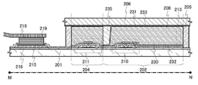
반도체 장치의 일 형태에 대해, 도 8 내지 도 10을 이용하여 설명한다. 도 8 내지 도 10은 도 7(B)의 M-N선에서의 단면도에 상당한다.One embodiment of the semiconductor device will be described with reference to FIGS. 8 to 10. 8-10 correspond to sectional drawing in the M-N line | wire of FIG. 7 (B).
도 8 내지 도 10에 나타내는 바와 같이, 반도체 장치는 접속 단자 전극(215) 및 단자 전극(216)을 가지고 있다. 접속 단자 전극(215) 및 단자 전극(216)은 FPC(218)가 가지는 단자와 이방성 도전층(219)을 통하여, 전기적으로 접속되어 있다.8 to 10, the semiconductor device has a connecting
접속 단자 전극(215)은 제 1 전극(230)과 같은 도전층으로 형성된다. 단자 전극(216)은 트랜지스터(210), 트랜지스터(211)의 소스 전극 및 드레인 전극과 같은 도전층으로 형성되어 있다.The
또 제 1 기판(201) 위에 형성된 화소부(202)와 주사선 구동 회로(204)의 각각은 트랜지스터를 복수 가지고 있다. 도 8 내지 도 10에서는, 화소부(202)에 포함되는 트랜지스터(210)와, 주사선 구동 회로(204)에 포함되는 트랜지스터(211)를 예시하고 있다.Each of the
*본 실시형태에서는, 트랜지스터(210), 트랜지스터(211)로서, 실시형태 1에 설명한 트랜지스터를 적용할 수 있다. 트랜지스터(210), 트랜지스터(211)는 전기적 특성 변동이 억제되어 있어 전기적으로 안정적이다. 전술한 바와 같이, 도 8 내지 도 10에 나타내는 본 실시형태의 반도체 장치로서 신뢰성이 높은 반도체 장치를 제공할 수 있다.In this embodiment, the transistors described in
화소부(202)에 설치된 트랜지스터(210)는 표시 소자와 전기적으로 접속하여, 표시 패널을 구성한다. 표시 소자는 표시를 행할 수 있다면 특별히 한정되지 않고, 다양한 표시 소자를 이용할 수 있다.The
도 8에 표시 소자로서 액정 소자를 이용한 액정 표시 장치의 예를 나타낸다. 도 8에서, 표시 소자인 액정 소자(213)는 제 1 전극(230), 제 2 전극(231), 및 액정층(208)을 포함한다. 또한 액정층(208)을 협지하도록 배향층으로서 기능하는 절연층(232, 233)이 형성되어 있음을 주목하라. 제 2 전극(231)은 제 2 기판(206)측에 설치된다. 제 1 전극(230)과 제 2 전극(231)은 협지된 액정층(208)을 통하여 적층하는 구성으로 되어 있다.The example of the liquid crystal display device using a liquid crystal element as a display element is shown in FIG. In FIG. 8, the
또, 스페이서(235)는 절연층을 선택적으로 에칭함으로써 얻어지는 주상의(columnar) 스페이서이며, 액정층(208)의 두께(셀 갭)를 제어하기 위해 설치되어 있다. 또한 구상의(spherical) 스페이서를 이용해도 좋다.The
표시 소자로서 액정 소자를 이용하는 경우, 서모트로픽 액정, 저분자 액정, 고분자 액정, 고분자 분산형 액정, 강유전성 액정, 반강유전성 액정 등을 이용한다. 이러한 액정 재료는, 조건에 따라, 콜레스테릭상, 스멕틱상, 큐빅상, 카이럴 네마틱상, 등방상 등을 나타낸다.When using a liquid crystal element as a display element, a thermotropic liquid crystal, a low molecular liquid crystal, a polymer liquid crystal, a polymer dispersion type liquid crystal, a ferroelectric liquid crystal, an antiferroelectric liquid crystal, etc. are used. Such a liquid crystal material shows a cholesteric phase, a smectic phase, a cubic phase, a chiral nematic phase, an isotropic phase, etc. according to conditions.
또, 배향층이 불필요한 블루상을 나타내는 액정을 이용해도 좋다. 블루상은 액정상의 하나로서, 콜레스테릭 액정을 승온해 가면, 콜레스테릭상으로부터 등방상으로 전이하기 직전에 발현하는 상이다. 블루상은 좁은 온도 범위에서밖에 발현하지 않기 때문에, 온도 범위를 개선하기 위해 카이럴제를 혼합시킨 액정 조성물을 액정층에 이용한다. 블루상을 나타내는 액정과 카이럴제를 포함하는 액정 조성물은 응답 속도가 1 msec 이하로 짧고, 광학적 등방성이기 때문에 배향 처리가 불필요하고, 시야각 의존성이 작다. 또한 배향층을 형성하지 않아도 되므로 러빙 처리도 불필요해지기 때문에, 러빙 처리에 의해 발생되는 정전 방전 파괴를 방지할 수 있어, 제작 공정 중의 액정 표시 장치의 불량이나 파손을 경감할 수 있다. 따라서 액정 표시 장치의 생산성을 향상시키는 것이 가능하게 된다.Moreover, you may use the liquid crystal which shows an unnecessary blue phase of an orientation layer. The blue phase is one of the liquid crystal phases. When the temperature of the cholesteric liquid crystal is raised, the blue phase is a phase which is expressed immediately before transition from the cholesteric phase to the isotropic phase. Since a blue phase expresses only in a narrow temperature range, in order to improve a temperature range, the liquid crystal composition which mixed the chiral agent is used for a liquid crystal layer. The liquid crystal composition containing the liquid crystal showing a blue phase and a chiral agent has a short response speed of 1 msec or less, and because of its optical isotropy, no alignment treatment is necessary and the viewing angle dependency is small. In addition, since the alignment layer does not have to be formed, the rubbing process is also unnecessary, so that the electrostatic discharge breakdown caused by the rubbing process can be prevented, and the defect or damage of the liquid crystal display device during the manufacturing process can be reduced. Therefore, it becomes possible to improve productivity of a liquid crystal display device.
또, 액정 재료의 고유 저항율은 1×10⁹ Ω·cm 이상이며, 바람직하게는 1×10¹¹ Ω·cm 이상이며, 더욱 바람직하게는 1×10¹² Ω·cm 이상이다. 또한 본 명세서에서의 고유 저항율의 값은 20℃에서 측정한 값으로 함을 주목하라.The resistivity of the liquid crystal material is 1 × 10 9 Ω · cm or more, preferably 1 × 10 11 Ω · cm or more, and more preferably 1 × 10 12 Ω · cm or more. Note that the value of the specific resistivity in the present specification is a value measured at 20 ° C.
액정 표시 장치에 형성되는 보유 용량의 크기는, 화소부에 배치되는 트랜지스터의 리크 전류 등을 고려하여, 소정의 기간 동안 전하를 보유할 수 있도록 설정된다. 고순도의 산화물 반도체층을 가지는 트랜지스터를 이용함으로써, 각 화소에서의 액정 용량에 대하여 1/3 이하, 바람직하게는 1/5 이하의 용량의 크기를 가지는 보유 용량을 형성하면 충분하다.The size of the storage capacitor formed in the liquid crystal display device is set to be able to retain electric charges for a predetermined period in consideration of the leak current of the transistor disposed in the pixel portion. By using a transistor having a high purity oxide semiconductor layer, it is sufficient to form a storage capacitor having a size of 1/3 or less, preferably 1/5 or less of the liquid crystal capacitance in each pixel.
본 실시형태에 이용하는 고순도화된 산화물 반도체층을 이용한 트랜지스터는 오프 상태에서의 전류값(오프 전류값)을 낮게 할 수 있다. 그러므로, 화상 신호 등의 전기 신호의 보유 시간을 길게 할 수 있고, 전원 온 상태에서는 기입 간격도 길게 설정할 수 있다. 따라서, 리프레시 동작의 빈도를 줄일 수 있기 때문에, 소비 전력을 억제하는 효과를 얻는다.The transistor using the highly purified oxide semiconductor layer used in the present embodiment can lower the current value (off current value) in the off state. Therefore, the retention time of electric signals such as image signals can be lengthened, and the writing interval can also be set long in the power-on state. Therefore, since the frequency of the refresh operation can be reduced, the effect of suppressing power consumption is obtained.
또, 본 실시형태에 이용하는 고순도화된 산화물 반도체층을 이용한 트랜지스터는, 비교적 높은 전계 효과 이동도를 얻을 수 있기 때문에, 고속 구동이 가능하다. 따라서, 액정 표시 장치의 화소부에 상기 트랜지스터를 이용함으로써, 고화질의 화상을 제공할 수 있다. 또, 상기 트랜지스터는 동일 기판 위에 구동 회로부 또는 화소부에 나누어 만들어 제작할 수 있기 때문에, 액정 표시 장치의 부품 점수를 삭감할 수 있다.In addition, since the transistor using the highly purified oxide semiconductor layer used in the present embodiment can obtain a relatively high field effect mobility, high-speed driving is possible. Therefore, by using the transistor in the pixel portion of the liquid crystal display device, a high quality image can be provided. In addition, since the transistor can be made and manufactured by dividing the driving circuit portion or the pixel portion on the same substrate, the component score of the liquid crystal display device can be reduced.
액정 표시 장치에는, TN(Twisted Nematic) 모드, IPS(In-Plane-Switching) 모드, FFS(Fringe Field Switching) 모드, ASM(Axially Symmetricaligned Micro-cell) 모드, OCB(Optical Compensated Birefringence) 모드, FLC(Ferroelectric Liquid Crystal) 모드, AFLC(AntiFerroelectric Liquid Crystal) 모드 등을 이용한다.The liquid crystal display includes twisted nematic (TN) mode, in-plane-switching (IPS) mode, fringe field switching (FSF) mode, axially symmetric aligned micro-cell (ASM) mode, optically-compensated birefringence (OCB) mode, and FLC (FLC). Ferroelectric Liquid Crystal (AFR) mode, Antiferroelectric Liquid Crystal (AFLC) mode and the like are used.
또, 노멀리-블랙형의 액정 표시 장치, 예를 들면 수직 배향(VA) 모드를 채용한 투과형의 액정 표시 장치로 해도 좋다. 여기서, 수직 배향 모드란, 액정 표시 패널의 액정 분자의 배열을 제어하는 방식의 일종이며, 전압이 인가되어 있지 않을 때에 패널면에 대하여 액정 분자가 수직 방향을 향하는 방식이다. 수직 배향 모드로서는 몇 개의 예를 들고 있지만, 예를 들면, MVA(Multi-Domain Vertical Alignment) 모드, PVA(Patterned Vertical Alignment) 모드, ASV 모드 등을 이용한다. 또, 화소(픽셀)를 몇 개의 영역(서브 픽셀)으로 나누어, 각각 다른 영역에서 분자를 다른 방향으로 배향되도록 고안되어 있는 멀티 도메인화 혹은 멀티 도메인 설계라고 불리는 방법을 이용한다.Moreover, it is good also as a transmission-type liquid crystal display device which employ | adopts a normally-black type liquid crystal display device, for example, a vertical alignment (VA) mode. Here, a vertical alignment mode is a kind of system which controls the arrangement | sequence of the liquid crystal molecule of a liquid crystal display panel, and is a system in which a liquid crystal molecule faces a perpendicular direction with respect to a panel surface when a voltage is not applied. Some examples are given as the vertical alignment mode. For example, a multi-domain vertical alignment (MVA) mode, a patterned vertical alignment (PVA) mode, an ASV mode, and the like are used. In addition, a method called multi-domainization or multi-domain design is used in which pixels (pixels) are divided into several regions (sub pixels), and molecules are designed to be oriented in different directions in different regions.
또, 표시 장치에 있어서, 블랙 매트릭스(차광층), 편광 부재, 위상차 부재, 반사 방지 부재 등의 광학 부재(광학 기판) 등은 적절히 형성한다. 예를 들면, 편광 기판 및 위상차 기판에 의한 원 편광을 이용해도 좋다. 또, 광원으로서 백 라이트, 사이드 라이트 등을 이용해도 좋다.In the display device, an optical member (optical substrate) such as a black matrix (light shielding layer), a polarizing member, a retardation member, an antireflection member, or the like is appropriately formed. For example, circular polarization by a polarizing substrate and a retardation substrate may be used. Moreover, you may use a backlight, a side light, etc. as a light source.
또, 백 라이트로서 복수의 발광 다이오드(LED)를 이용하여, 시간 분할 표시 방식(필드 시퀀셜 구동 방식)을 행하는 것도 가능하다. 필드 시퀀셜 구동 방식을 적용함으로써, 컬러 필터를 이용하지 않고, 컬러 표시를 행하는 것이 가능하다.It is also possible to perform a time division display method (field sequential drive method) using a plurality of light emitting diodes (LEDs) as the backlight. By applying the field sequential driving method, it is possible to perform color display without using a color filter.
또, 화소부에서의 표시 방식은, 프로그래시브 방식이나 인터레이스 방식 등을 이용한다. 또, 컬러 표시할 때에 화소에서 제어하는 색요소로서는, RGB(R은 적, G는 녹, B는 청을 나타냄)의 삼색에 한정되지 않는다. 예를 들면, RGBW(W는 흰색을 나타냄), 또는 RGB에, 옐로우, 시안, 마젠타 등을 일색 이상 추가한 것이 있다. 또한 색요소의 도트마다 그 표시 영역의 크기가 상이하여도 좋다. 단, 본 발명은 컬러 표시의 표시 장치에 한정되는 것은 아니고, 모노크롬 표시의 표시 장치에 적용할 수도 있음을 주목하라.As the display method in the pixel portion, a progressive method, an interlace method, or the like is used. In addition, the color element controlled by the pixel during color display is not limited to three colors of RGB (R is red, G is green, and B is blue). For example, RGBW (W represents white) or RGB, yellow, cyan, magenta, etc. are added by one or more colors. In addition, the size of the display area may be different for each dot of the color element. Note that the present invention is not limited to the display device of the color display, but can also be applied to the display device of the monochrome display.
또, 표시 장치에 포함되는 표시 소자로서, 일렉트로루미네선스를 이용하는 발광 소자를 적용해도 좋다. 일렉트로루미네선스를 이용하는 발광 소자는 발광 재료가 유기 화합물인지, 무기 화합물인지에 따라 구별되고, 일반적으로, 전자는 유기 EL 소자, 후자는 무기 EL 소자라고 불린다.Moreover, you may apply the light emitting element using electroluminescence as a display element contained in a display apparatus. The light emitting element using the electroluminescence is classified according to whether the light emitting material is an organic compound or an inorganic compound, and in general, the former is called an organic EL element, and the latter is called an inorganic EL element.
유기 EL 소자는, 발광 소자에게 전압을 인가함으로써, 한 쌍의 전극으로부터 전자 및 정공이 각각 발광성의 유기 화합물을 포함하는 층에 주입되어 전류가 흐른다. 그리고, 이들 캐리어(전자 및 정공)가 재결합함으로써, 발광한다. 이러한 메카니즘으로부터, 이러한 발광 소자는 전류 여기형의 발광 소자라고 불린다.In the organic EL element, a voltage is applied to the light emitting element, whereby electrons and holes are injected into a layer containing a light emitting organic compound from a pair of electrodes, respectively, and a current flows. Then, these carriers (electrons and holes) recombine to emit light. From this mechanism, such a light emitting element is called a current excitation type light emitting element.
무기 EL 소자는 그 소자 구성에 따라, 분산형 무기 EL 소자와 박막형 무기 EL 소자로 분류된다. 분산형 무기 EL 소자는, 발광 재료의 입자를 바인더 중에 분산시킨 발광층을 가지는 것이고, 발광 메카니즘은 도너 준위와 억셉터 준위를 이용하는 도너-억셉터 재결합형 발광이다. 박막형 무기 EL 소자는 발광층을 유전체층으로 끼우고, 그것을 다시 전극으로 끼운 구조이며, 발광 메카니즘은 금속 이온의 내각 전자 천이를 이용하는 국지형 발광이다. 또한 여기에서는, 발광 소자로서 유기 EL 소자를 이용하여 설명함을 주목하라.Inorganic EL elements are classified into dispersion type inorganic EL elements and thin film type inorganic EL elements according to their element configurations. A dispersed inorganic EL device has a light emitting layer in which particles of a light emitting material are dispersed in a binder, and a light emitting mechanism is donor-acceptor recombination type light emission using a donor level and an acceptor level. The thin-film inorganic EL device has a structure in which a light emitting layer is sandwiched with a dielectric layer and then sandwiched with an electrode, and the light emitting mechanism is localized light emission utilizing internal electron transition of metal ions. Note that here, the description will be made using an organic EL element as a light emitting element.
발광 소자는 광을 꺼내기 위해 적어도 한 쌍의 전극의 한쪽이 투명하면 좋다. 그리고, 기판 위에 트랜지스터 및 발광 소자가 형성된다. 기판과는 반대측의 면으로부터 광을 꺼내는 상면 사출이나, 기판측의 면으로부터 광을 꺼내는 하면 사출이나, 기판측 및 기판과는 반대측의 면으로부터 광을 꺼내는 양면 사출 구조의 발광 소자가 있고, 어느 사출 구조의 발광 소자를 적용해도 좋다.At least one of the pair of electrodes may be transparent for the light emitting element to extract light. Then, a transistor and a light emitting element are formed on the substrate. There is a light emitting device having an upper surface ejection for extracting light from the surface opposite to the substrate, a lower surface ejection for extracting light from the surface on the substrate side, or a light emitting element having a double-sided ejection structure for extracting light from the surface on the opposite side to the substrate and the substrate. You may apply the light emitting element of a structure.
도 9에 표시 소자로서 발광 소자를 고용한 발광 장치의 예를 나타낸다. 표시 소자인 발광 소자(243)는 화소부(202)에 설치된 트랜지스터(210)와 전기적으로 접속하고 있다. 또한 발광 소자(243)의 구성은 제 1 전극(230), 전계 발광층(241), 제 2 전극(231)의 적층 구조이지만, 도 9에 나타낸 적층 구성에 한정되지 않는다. 발광 소자(243)로부터 꺼내는 광의 방향 등에 맞추어, 발광 소자(243)의 구성은 적절히 바꾸어도 좋다.9 shows an example of a light emitting device employing a light emitting element as a display element. The
격벽(240)은 유기 절연 재료, 또는 무기 절연 재료를 이용하여 형성한다. 특히 감광성의 수지 재료를 이용하여, 제 1 전극(230) 위에 개구부를 형성하고, 그 개구부의 측벽을 연속한 곡률을 가지는 경사면으로 하는 것이 바람직하다.The
전계 발광층(241)은 단수의 층으로 구성되어 있어도, 복수의 층이 적층되도록 구성되어 있어도 어느 쪽이어도 좋다.The
발광 소자(243)에 산소, 수소, 수분, 이산화탄소 등이 침입하지 않도록, 제 2 전극(231) 및 격벽(240) 위에 보호층을 형성해도 좋다. 보호층으로서는, 질화 실리콘층, 질화 산화 실리콘층, DLC(Diamond Like Carbon)층 등을 들 수 있다. 또, 제 1 기판(201), 제 2 기판(206), 및 시일재(205)에 의해 봉지된 공간에는 충전재(244)가 형성되어 밀봉되어 있다. 이와 같이 외기에 노출되지 않도록 기밀성이 높고, 탈가스가 적은 보호 필름(부착 필름, 자외선 경화 수지 필름 등)이나 커버재로 패키징(봉입(sealed))하는 것이 바람직하다.A protective layer may be formed on the
충전재(244)로서는 질소나 아르곤 등의 불활성 가스 외에, 자외선 경화 수지 또는 열경화 수지를 이용해도 좋다. 예를 들면, PVC(폴리비닐 클로라이드), 아크릴 수지, 폴리이미드 수지, 에폭시 수지, 실리콘 수지, PVB(폴리비닐부티랄) 또는 EVA(에틸렌 비닐 아세테이트) 등을 이용한다.As the
또한, 필요하다면, 발광 소자의 사출면에 편광판, 또는 원 편광판(타원 편광판을 포함함), 위상차판(λ/4판, λ/2판), 컬러 필터 등의 광학 필름을 적절히 제공해도 좋다. 또, 편광판 또는 원 편광판에 반사 방지층을 형성해도 좋다. 예를 들면, 표면의 요철에 의해 반사광을 확산하여, 비침을 저감할 수 있는 안티글레어(anti-glare) 처리를 실시해도 좋다.If necessary, optical films such as polarizing plates or circular polarizing plates (including elliptical polarizing plates), retardation plates (λ / 4 plates, λ / 2 plates) and color filters may be appropriately provided on the emitting surface of the light emitting element. Moreover, you may provide an antireflection layer in a polarizing plate or a circularly polarizing plate. For example, anti-glare treatment may be performed to diffuse reflected light due to unevenness of the surface and to reduce non-glare.
또, 표시 장치로서 전자 잉크를 구동시키는 전자 페이퍼를 제공하는 것도 가능하다. 전자 페이퍼는 전기 영동(泳動) 표시 장치(전기 영동 디스플레이)라고도 불리고, 종이와 같이 읽기에 편하고, 다른 표시 장치에 비해 저소비 전력이며, 얇고 가벼운 형상으로 하는 것이 가능하다는 이점을 가지고 있다.Moreover, it is also possible to provide the electronic paper which drives an electronic ink as a display apparatus. Electronic paper is also called an electrophoretic display (electrophoretic display) and has the advantage of being easy to read like a paper, low power consumption compared to other display devices, and having a thin and light shape.
전기 영동 표시 장치는 다양한 형태를 생각할 수 있다. 전기 영동 표시 장치는 플러스의 전하를 가지는 제 1 입자와, 마이너스의 전하를 가지는 제 2 입자를 포함하는 마이크로 캡슐이 용매 또는 용질에 복수 분산된 것이다. 마이크로 캡슐에 전계를 인가하는 것에 의해, 마이크로 캡슐 중의 입자를 서로 반대 방향으로 이동시키고, 한쪽에 집합한 입자의 색만을 표시하는 것이다. 또한 제 1 입자 또는 제 2 입자는 염료를 포함하고, 전계가 없는 경우에 이동하지 않는 것임을 주목하라. 또, 제 1 입자의 색과 제 2 입자의 색은 서로 다른 것(무색을 포함함)으로 한다.Electrophoretic display devices can take various forms. In the electrophoretic display, a plurality of microcapsules including a first particle having a positive charge and a second particle having a negative charge are dispersed in a solvent or a solute. By applying an electric field to the microcapsules, the particles in the microcapsules are moved in opposite directions to display only the color of the particles collected on one side. Note also that the first or second particles contain dyes and do not migrate in the absence of an electric field. The color of the first particles and the color of the second particles are different from each other (including colorlessness).
이와 같이, 전기 영동 표시 장치는, 유전정수가 높은 물질이 높은 전계 영역으로 이동하는, 소위 유전 영동적 효과를 이용한 디스플레이이다.As described above, the electrophoretic display is a display using a so-called dielectric electrophoretic effect in which a substance having a high dielectric constant moves to a high electric field region.
상기 마이크로 캡슐을 용매 중에 분산시킨 것이 전자 잉크라고 불리는 것이다. 이 전자 잉크는 유리, 플라스틱, 천, 종이 등의 표면에 인쇄할 수 있다. 또, 컬러 필터나 색소를 가지는 입자를 이용하는 것에 의해 컬러 표시도 가능하다.Dispersion of the microcapsules in a solvent is called an electronic ink. This electronic ink can be printed on the surface of glass, plastic, cloth, paper, or the like. Moreover, color display is also possible by using the particle | grains which have a color filter and a pigment | dye.
또한 마이크로 캡슐 중의 제 1 입자 및 제 2 입자는, 도전체 재료, 절연체 재료, 반도체 재료, 자성 재료, 액정 재료, 강유전성 재료, 일렉트로루미네센트 재료, 일렉트로크로믹 재료, 자기 영동 재료로부터 선택된 일종의 재료 또는 이들의 복합 재료를 이용하면 좋음을 주목하라.The first particles and the second particles in the microcapsules are a kind of material selected from a conductor material, an insulator material, a semiconductor material, a magnetic material, a liquid crystal material, a ferroelectric material, an electroluminescent material, an electrochromic material, and a magnetophoretic material. Or note that using these composite materials is good.
또, 전자 페이퍼로서, 트위스트 볼 표시 방식을 이용하는 표시 장치를 적용해도 좋다. 트위스트 볼 표시 방식이란, 백과 흑으로 나누어 도포된 구형 입자를 표시 소자에 이용하는 전극인 제 1 전극 및 제 2 전극의 사이에 배치하고, 제 1 전극과 제 2 전극 사이에 전위차를 일으켜 구형 입자의 방향을 제어함으로써, 표시를 행하는 방법이다.Moreover, you may apply the display apparatus which uses the twist ball display system as an electronic paper. The twist ball display system is arranged between a first electrode and a second electrode, which is an electrode used for a display element, to arrange spherical particles coated in white and black, and to generate a potential difference between the first electrode and the second electrode, and thus the direction of the spherical particles. It is a method of displaying by controlling.
도 10에, 반도체 장치의 일 형태로서 액티브 매트릭스형의 전자 페이퍼를 나타낸다. 도 10의 전자 페이퍼는, 트위스트 볼 표시 방식을 이용한 표시 장치의 예이다.10 shows an active matrix electronic paper as one embodiment of a semiconductor device. The electronic paper in FIG. 10 is an example of a display device using a twist ball display system.
트랜지스터(210)와 접속하는 제 1 전극(230)과, 제 2 기판(206)에 설치된 제 2 전극(231)의 사이에는, 흑색 영역(255a) 및 백색 영역(255b)을 가지고, 주위에 액체로 채워져 있는 캐비티(252)를 포함하는 구형 입자(253)가 형성되어 있다. 구형 입자(253)의 주위는 수지 등의 충전재(254)로 충전되어 있다. 제 2 전극(231)이 공통 전극(대향 전극)에 상당한다. 제 2 전극(231)은 공통 전위선과 전기적으로 접속된다.It has a
또한 도 8 내지 도 10에서, 제 1 기판(201), 제 2 기판(206)으로서는 유리 기판 외에, 가요성을 가지는 기판이 이용될 수 있다. 예를 들면 투광성을 가지는 플라스틱 기판 등을 이용한다. 플라스틱으로서는, FRP(Fiberglass-Reinforced Plastics)판, PVF(폴리비닐 플루오라이드) 필름, 폴리에스테르 필름 또는 아크릴 수지 필름을 이용한다. 또, 알루미늄 포일을 PVF 필름이나 폴리에스테르 필름으로 끼운 구조의 시트를 이용해도 좋다.8 to 10, in addition to the glass substrate, a substrate having flexibility may be used as the
절연층(221)은 무기 절연 재료 또는 유기 절연 재료를 이용하여 형성한다. 또한 아크릴 수지, 폴리이미드 수지, 벤조시클로부텐 수지, 폴리아미드 수지, 에폭시 수지 등의 내열성을 가지는 유기 절연 재료를 이용하면, 평탄화 절연층으로서 적합함을 주목하라. 또한 상기 유기 절연 재료 외에, 저유전율 재료(low-k 재료), 실록산계 수지, PSG(phosphosilicate glass:인 유리), BPSG(borophosphosilicate glass:인 붕소 유리) 등을 이용한다. 또한 이러한 재료로 구성되는 절연층을 복수 적층하여, 절연층(221)으로 해도 좋다.The insulating
절연층(221)의 성막법은 특별히 한정되지 않고, 그 재료에 따라, 스퍼터링법, 스핀 코트법, 디핑법, 스프레이 도포, 액적 토출법(잉크젯법, 스크린 인쇄, 오프셋 인쇄 등), 롤 코팅, 커튼 코팅, 나이프 코팅 등을 이용한다.The film forming method of the insulating
표시 장치는 광원 또는 표시 소자로부터의 광을 투과시켜 표시를 행한다. 따라서 광이 투과하는 화소부에 설치되는 기판과, 절연층, 도전층 등의 박막은 모두 가시광의 파장 영역의 광에 대하여 투광성으로 한다.The display device transmits light from a light source or a display element to perform display. Therefore, both the substrate and the thin film such as the insulating layer and the conductive layer, which are provided in the pixel portion through which the light is transmitted, are transparent to the light in the wavelength region of the visible light.
표시 소자에 전압을 인가하는 제 1 전극 및 제 2 전극(화소 전극, 공통 전극, 대향 전극 등이라고도 함)에서는, 꺼내는 광의 방향, 전극이 설치되는 장소, 및 전극의 패턴 구조에 의해 투광성, 반사성을 선택하면 좋다.In the first electrode and the second electrode (also called pixel electrode, common electrode, counter electrode, etc.) for applying a voltage to the display element, light transmittance and reflectivity are determined by the direction of the light to be taken out, the place where the electrode is installed, and the pattern structure of the electrode. Good to choose.
제 1 전극(230), 제 2 전극(231)에는, 산화 텅스텐을 포함하는 인듐 산화물, 산화 텅스텐을 포함하는 인듐 아연 산화물, 산화 티탄을 포함하는 인듐 산화물, 산화 티탄을 포함하는 인듐 주석 산화물, 인듐 주석 산화물(이하, ITO라고 나타냄), 인듐 아연 산화물, 산화 규소를 첨가한 인듐 주석 산화물 등의 투광성을 가지는 도전성 재료를 이용한다.The
또, 제 1 전극(230), 제 2 전극(231)은 텅스텐(W), 몰리브덴(Mo), 지르코늄(Zr), 하프늄(Hf), 바나듐(V), 니오브(Nb), 탄탈(Ta), 크롬(Cr), 코발트(Co), 니켈(Ni), 티탄(Ti), 백금(Pt), 알루미늄(Al), 구리(Cu), 은(Ag) 등의 금속, 또는 그 합금, 혹은 그 질화물로부터 하나, 또는 복수종을 이용한다.In addition, the
또, 제 1 전극(230), 제 2 전극(231)으로서, 도전성 고분자(도전성 폴리머라고도 함)를 포함하는 도전성 조성물을 이용한다. 도전성 고분자로서는, 소위 π전자 공액계 도전성 고분자를 이용해도 좋다. 예를 들면, 폴리아닐린 혹은 그 유도체, 폴리피롤 혹은 그 유도체, 폴리티오펜 혹은 그 유도체, 또는 아닐린, 피롤 및 티오펜의 2종 이상으로 이루어지는 공중합체 혹은 그 유도체 등을 들 수 있다.As the
또, 트랜지스터는 정전기 등에 의해 파괴되기 쉽기 때문에, 구동 회로 보호용의 보호 회로를 형성하는 것이 바람직하다. 보호 회로는, 비선형 소자를 이용하여 구성하는 것이 바람직하다.In addition, since the transistor is easily broken by static electricity or the like, it is preferable to form a protection circuit for driving circuit protection. It is preferable to comprise a protection circuit using a nonlinear element.
이상과 같이 실시형태 1에 예시한 트랜지스터를 적용함으로써, 소비 전력이 작고, 또한 신뢰성이 높은 반도체 장치를 제공할 수 있다. 또한 실시형태 1에 예시한 트랜지스터는 상술한 표시 기능을 가지는 반도체 장치뿐만 아니라, 전원 회로에 탑재되는 파워 디바이스, LSI 등의 반도체 집적 회로, 대상물의 정보를 읽어내는 이미지 센서 기능을 가지는 반도체 장치 등 다양한 기능을 가지는 반도체 장치에 적용하는 것이 가능함을 주목하라.By applying the transistors exemplified in
이상, 본 실시형태에 나타내는 구성, 방법 등은, 다른 실시형태에 나타내는 구성, 방법 등과 적절히 조합하여 이용해도 좋다.As mentioned above, you may use the structure, method, etc. which are shown in this embodiment suitably in combination with the structure, method, etc. which are shown in another embodiment.
(실시형태 3)(Embodiment 3)
본 발명의 일 양태인 반도체 장치는, 다양한 전자기기(유기기도 포함함)에 적용할 수 있다. 전자기기로서는, 예를 들면, 텔레비전 장치(텔레비전 또는 텔레비전 수신기라고도 함), 컴퓨터용 등의 모니터, 디지털 카메라, 디지털 비디오 카메라 등의 카메라, 디지털 포토 프레임, 휴대전화기(휴대전화, 휴대전화 장치라고도 함), 휴대형 게임기, 휴대 정보 단말, 음향 재생장치, 파칭코기 등의 대형 게임기 등을 들 수 있다. 상기 실시형태에 설명한 반도체 장치를 구비하는 전자기기의 예에 대하여 설명한다.The semiconductor device of one embodiment of the present invention can be applied to various electronic devices (including organic devices). As the electronic device, for example, a television device (also called a television or a television receiver), a monitor for a computer, a camera such as a digital camera, a digital video camera, a digital photo frame, a mobile phone (also called a mobile phone or a mobile phone device). ), A large game machine such as a portable game machine, a portable information terminal, a sound reproducing apparatus, and a paching nose machine. An example of an electronic device including the semiconductor device described in the above embodiment will be described.
도 11(A)은 노트형의 퍼스널 컴퓨터이며, 본체(301), 하우징(302), 표시부(303), 키보드(304) 등에 의해 구성되어 있다. 실시형태 1 또는 2에 나타낸 반도체 장치를 적용함으로써, 신뢰성이 높은 노트형의 퍼스널 컴퓨터로 할 수 있다.Fig. 11A is a notebook personal computer, which is composed of a
도 11(B)은 휴대 정보 단말(PDA)이며, 본체(311)에는 표시부(313)와 외부 인터페이스(315)와 조작 버튼(314) 등이 설치되어 있다. 또 조작용의 부속품으로서 스타일러스(312)가 있다. 실시형태 1 또는 2에 나타낸 반도체 장치를 적용함으로써, 보다 신뢰성이 높은 휴대 정보 단말(PDA)로 할 수 있다.Fig. 11B is a portable information terminal PDA, and the
도 11(C)은 전자 서적의 일례를 나타낸다. 예를 들면, 전자 서적(320)은 하우징(321) 및 하우징(322)의 2개의 하우징으로 구성되어 있다. 하우징(321) 및 하우징(322)은 축부(325)에 의해 일체로 되어 있고, 이 축부(325)를 축으로 하여 개폐 동작을 행할 수 있다. 이러한 구성에 의해, 전자 서적(320)은 종이 서적과 같은 동작을 행하는 것이 가능해진다.11C shows an example of an electronic book. For example, the
하우징(321)에는 표시부(323)가 조립되고, 하우징(322)에는 표시부(324)가 각각 조립되어 있다. 표시부(323) 및 표시부(324)는 연속된 화면을 표시하는 구성으로 해도 좋고, 다른 화면을 표시하는 구성으로 해도 좋다. 다른 화면을 표시하는 구성으로 함으로써, 예를 들면 우측의 표시부(도 11(C)에서는 표시부(323))에 문장을 표시하고, 좌측의 표시부(도 11(C)에서는 표시부(324))에 화상을 표시할 수 있다. 실시형태 1 또는 2에 나타낸 반도체 장치를 적용함으로써, 신뢰성이 높은 전자 서적(320)으로 할 수 있다.The
또, 도 11(C)에서는, 하우징(321)에 조작부 등을 구비한 예를 나타낸다. 예를 들면, 하우징(321)에서 전원(326), 조작 키(327), 스피커(328) 등을 구비하고 있다. 조작 키(327)에 의해, 페이지를 넘길 수 있다. 또한 하우징의 표시부와 동일면에 키보드나 포인팅 디바이스 등을 구비하는 구성으로 해도 좋음을 주목하라. 또, 하우징의 이면이나 측면에, 외부 접속용 단자(이어폰 단자, USB 단자 등), 기록 매체 삽입부 등을 구비하는 구성으로 해도 좋다. 또한 전자 서적(320)은 전자 사전으로서의 기능을 갖게 한 구성으로 해도 좋다.11C shows an example in which the
또, 전자 서적(320)은 무선으로 정보를 송수신할 수 있는 구성으로 해도 좋다. 무선에 의해, 전자 서적 서버로부터 원하는 서적 데이터 등을 구입하여, 다운로드하는 구성으로 하는 것도 가능하다.The
도 11(D)은 휴대전화이며, 하우징(330) 및 하우징(331)의 2개의 하우징으로 구성되어 있다. 하우징(331)에는, 표시 패널(332), 스피커(333), 마이크로폰(334), 포인팅 디바이스(336), 카메라용 렌즈(337), 외부 접속 단자(338) 등을 구비하고 있다. 또, 하우징(330)에는 휴대형 정보단말기의 충전을 행하는 태양전지 셀(340), 외부 메모리 슬롯(341) 등을 구비하고 있다. 또, 안테나는 하우징(331) 내부에 내장되어 있다. 실시형태 1 또는 2에 나타낸 반도체 장치를 적용함으로써, 신뢰성이 높은 휴대전화로 할 수 있다.FIG. 11D illustrates a mobile phone and is composed of two housings, a
또, 표시 패널(332)은 터치 패널을 구비하고 있고, 도 11(D)에는 영상 표시되고 있는 복수의 조작 키(335)를 점선으로 나타낸다. 또한 휴대전화는 태양전지 셀(340)에서 출력되는 전압을 각 회로에 필요한 전압으로 승압하기 위한 승압 회로도 실장하고 있음을 주목하라.In addition, the
표시 패널(332)은 사용 형태에 따라 표시의 방향이 적절히 변화한다. 또, 휴대전화는 표시 패널(332)과 동일면 위에 카메라용 렌즈(337)를 구비하고 있기 때문에, 영상 통화가 가능하다. 스피커(333) 및 마이크로폰(334)은 음성 통화에 한정하지 않고, 영상 통화, 녹음, 재생 등이 가능하다. 또한 하우징(330)과 하우징(331)은 슬라이드하여, 도 11(D)과 같이 펼쳐진 상태로부터 서로 겹친 상태로 할 수 있어, 휴대에 적합한 소형화가 가능하다.In the
외부 접속 단자(338)는 AC 어댑터 및 USB 케이블 등의 각종 케이블과 접속 가능하고, 충전 및 퍼스널 컴퓨터 등과의 데이터 통신이 가능하다. 또, 외부 메모리 슬롯(341)에 기록 매체를 삽입하여, 보다 대량의 데이터 보존 및 이동에 대응할 수 있다.The
또, 상기 기능에 더하여, 적외선 통신 기능, 텔레비전 수신 기능 등을 구비한 것이어도 좋다.In addition to the above functions, an infrared communication function, a television reception function, or the like may be provided.
도 11(E)은 텔레비전 장치의 일례를 나타낸다. 텔레비전 장치(360)는 하우징(361)에 표시부(363)가 조립되어 있다. 표시부(363)에 의해, 영상을 표시하는 것이 가능하다. 또, 여기에서는, 스탠드(365)에 의해 하우징(361)을 지지한 구성을 나타내고 있다. 실시형태 1 또는 2에 나타낸 반도체 장치를 적용함으로써, 신뢰성이 높은 텔레비전 장치(360)로 할 수 있다.11E shows an example of a television apparatus. In the
텔레비전 장치(360)의 조작은 하우징(361)이 구비하는 조작 스위치나, 별체의 리모콘 조작기에 의해 행할 수 있다. 또한, 리모콘 조작기에, 이 리모콘 조작기로부터 출력하는 정보를 표시하는 표시부를 형성하는 구성으로 해도 좋다.Operation of the
또한 텔레비전 장치(360)는 수신기나 모뎀 등을 구비한 구성으로 함을 주목하라. 수신기에 의해 일반의 텔레비전 방송의 수신을 행할 수 있다. 또한 모뎀을 통하여 유선 또는 무선에 의한 통신 네트워크에 접속함으로써, 한방향(송신자로부터 수신자) 또는 쌍방향(송신자와 수신자간, 혹은 수신자들간 등)의 정보 통신을 행하는 것도 가능하다.Note that the
이상, 본 실시형태에 나타내는 구성, 방법 등은, 다른 실시형태에 나타내는 구성, 방법 등과 적절히 조합하여 이용해도 좋다.As mentioned above, you may use the structure, method, etc. which are shown in this embodiment suitably in combination with the structure, method, etc. which are shown in another embodiment.
[실시예 1]Example 1
본 실시예에서는, 기판으로부터 베이스 절연층을 통하여 산화물 반도체층으로 확산하는 수소에 대하여 설명한다.In this embodiment, hydrogen diffused from the substrate to the oxide semiconductor layer through the base insulating layer will be described.
본 실시예에서는, 유리 기판과, 유리 기판 위의 베이스 절연층과, 베이스 절연층 위의 산화물 반도체층에 있어서 2차 이온 질량분석법(SIMS:Secondary Ion Mass Spectrometry)에 의해, 수소 농도의 깊이 방향 분석을 행하였다.In this embodiment, the depth direction analysis of hydrogen concentration is performed by secondary ion mass spectrometry (SIMS) in the glass substrate, the base insulating layer on the glass substrate, and the oxide semiconductor layer on the base insulating layer. Was performed.
본 실시예에서는, 시료 4 내지 시료 7에서의 질량수가 1인 수소 농도의 깊이 방향 분석을 행하였다.In the present Example, the depth direction analysis of the hydrogen concentration whose mass number in Samples 4-7 is 1 was performed.
시료 4의 제작 방법을 나타낸다.The preparation method of
먼저, 유리 기판 위에 제 1 산화 실리콘층을 성막했다. 제 1 산화 실리콘층은 본 명세서에서의 베이스 절연층에 해당한다. 또한 제 1 산화 실리콘층의 성막 조건은 이하에 나타내는 바와 같음을 주목하라.First, the 1st silicon oxide layer was formed into a film on the glass substrate. The first silicon oxide layer corresponds to the base insulating layer in the present specification. Note that the film forming conditions of the first silicon oxide layer are as shown below.
·성막법:RF 스퍼터링법Formation method: RF sputtering method
·타겟:석영 타겟Target: Quartz target
·성막 가스:Ar(25 sccm), O2(25 sccm)Deposition gas: Ar (25 sccm), O 2 (25 sccm)
*·전력:1.5 kW(13.56 MHz)* Electric power: 1.5kW (13.56MHz)
·압력:0.4 PaPressure: 0.4 Pa
·T-S간 거리:60 mm· T-S distance: 60mm
·성막시 기판 온도:100℃Substrate temperature at the time of film formation: 100 degreeC
·두께:300 nmThickness: 300 nm
다음에, 제 1 산화 실리콘층 위에 산화물 반도체층을 성막했다.Next, an oxide semiconductor layer was formed on the first silicon oxide layer.
산화물 반도체층의 성막 조건을 이하에 나타낸다.The film forming conditions of the oxide semiconductor layer are shown below.
·성막법:DC 스퍼터링법Deposition method: DC sputtering method
·타겟:In-Ga-Zn-O(In2O3:Ga2O3:ZnO = 1:1:2[mol수비]) 타겟· Target: In-Ga-ZnO (In 2 O 3: Ga 2 O 3: ZnO = 1: 1: 2 [mol defense]) of the target
·성막 가스:Ar(30 sccm), O2(15 sccm)Deposition gas: Ar (30 sccm), O 2 (15 sccm)
*·전력:0.5 kW(DC)* Power: 0.5 kW (DC)
·압력:0.4 PaPressure: 0.4 Pa
·T-S간 거리:60 mm· T-S distance: 60mm
·성막시 기판 온도:200℃Substrate temperature during film formation: 200 ° C
·두께:100 nmThickness: 100 nm
다음에, 산화물 반도체층 위에 제 2 산화 실리콘층을 성막했다. 또한 제 2 산화 실리콘층의 성막 조건은 이하에 나타내는 바와 같음을 주목하라.Next, a second silicon oxide layer was formed on the oxide semiconductor layer. Note that the film forming conditions of the second silicon oxide layer are as shown below.
·성막법:RF 스퍼터링법Formation method: RF sputtering method
·타겟:석영 타겟Target: Quartz target
·성막 가스:Ar(25 sccm), O2(25 sccm)Deposition gas: Ar (25 sccm), O 2 (25 sccm)
·전력:1.5 kW(13.56 MHz)Power: 1.5 kW (13.56 MHz)
·압력:0.4 PaPressure: 0.4 Pa
·T-S간 거리:60 mm· T-S distance: 60mm
·성막시 기판 온도:100℃Substrate temperature at the time of film formation: 100 degreeC
·두께:100 nmThickness: 100 nm
또한 제 1 산화 실리콘층으로부터 제 2 산화 실리콘층의 성막 공정까지를 진공에서 연속으로 행하였음을 주목하라. 이상으로 시료 4를 완성했다.Note that the process from the first silicon oxide layer to the film formation of the second silicon oxide layer was continuously performed in a vacuum.
계속하여, 시료 5에 대하여 설명한다. 각층의 성막 방법에 대해서는 시료 4를 참작한다.Subsequently, Sample 5 will be described. For the method of film formation of each layer,
먼저, 제 1 산화 실리콘층을 성막하기 전의 유리 기판에 대해, 제 1 열처리를 행하였다. 제 1 열처리는, 1×10⁻⁵ Pa의 진공 중에서, 기판 온도를 400℃, 시간을 10분으로 했다.First, the 1st heat processing was performed with respect to the glass substrate before forming a 1st silicon oxide layer. In the first heat treatment, the substrate temperature was 400 ° C. and the time was 10 minutes in a vacuum of 1 × 10 −5 Pa.
다음에, 제 1 열처리 후, 제 1 산화 실리콘층을 성막했다.Next, after the first heat treatment, a first silicon oxide layer was formed.
다음에, 제 1 산화 실리콘층 위에 산화물 반도체층을 성막했다.Next, an oxide semiconductor layer was formed on the first silicon oxide layer.
다음에, 산화물 반도체층 위에 제 2 산화 실리콘층을 성막했다.Next, a second silicon oxide layer was formed on the oxide semiconductor layer.
제 1 열처리로부터 제 2 산화 실리콘층의 성막까지 공정을 진공에서 연속으로 행하였다. 전술한 바와 같이, 시료 5를 완성했다.The process was performed continuously in a vacuum from the first heat treatment to the deposition of the second silicon oxide layer. As described above, Sample 5 was completed.
여기서, 시료 4, 시료 5에 대하여 제 2 열처리를 행하여, 각각 시료 6, 시료 7을 얻게 된다. 제 2 열처리는 온도를 450℃, 시간을 1시간, 질소 분위기 중에서 행하였다.Here, 2nd heat treatment is performed with respect to the
시료 4 내지 시료 7에서의 제 1 열처리 및 제 2 열처리의 유무에 대해, 표 1에 나타낸다.Table 1 shows the presence or absence of the first heat treatment and the second heat treatment in
시료 4 내지 시료 7의 SIMS의 결과를 각각 도 15 내지 도 18에 나타낸다.도 15는 시료 4의 SIMS의 결과이다. 실선(1001)은 질량수가 1인 수소 농도를, 실선(1003)은 질량수가 30인 실리콘의 2차 이온 강도를, 실선(1005)은 질량수가 16인 산소의 2차 이온 강도를 나타낸다.도 16은 시료 5의 SIMS의 결과이다. 실선(1101)은 질량수가 1인 수소 농도를, 실선(1103)은 질량수가 30인 실리콘의 2차 이온 강도를, 실선(1105)은 질량수가 16인 산소의 2차 이온 강도를 나타낸다.The results of SIMS of
도 17은 시료 6의 SIMS의 결과이다. 실선(1201)은 질량수가 1인 수소 농도를, 실선(1203)은 질량수가 30인 실리콘의 2차 이온 강도를, 실선(1205)은 질량수가 16인 산소의 2차 이온 강도를 나타낸다.17 is a result of SIMS of Sample 6. FIG. The
도 18은 시료 7의 SIMS의 결과이다. 실선(1301)은 질량수가 1인 수소 농도를, 실선(1303)은 질량수가 30인 실리콘의 2차 이온 강도를, 실선(1305)은 질량수가 16인 산소의 2차 이온 강도를 나타낸다.18 is a result of SIMS of Sample 7. FIG. The
또한 범위(1011)는 제 2 산화 실리콘층을, 범위(1012)는 산화물 반도체층을, 범위(1013)는 제 1 산화 실리콘층을, 범위(1014)는 유리 기판을 나타낸다. 여기서, 산화 실리콘의 표준 샘플을 사용하여 수소 농도를 정량화했기 때문에, 질량수가 1인 수소 농도의 정량 범위는 범위(1011) 및 범위(1013)이다.In addition,
시료 4와 시료 5를 비교하면, 어느 시료도 유리 기판 부근에서의 제 1 산화 실리콘층 내에 수소 농도의 피크를 가지는 것을 알 수 있었다. 피크에서의 수소 농도는 시료 4에서 3.7×10²⁰ atoms/cm3, 시료 5에서 1.1×10²⁰ atoms/cm3였다.Comparing
시료 4와 시료 6을 비교하면, 시료 6에서는 제 1 산화 실리콘층 내인 깊이 500 nm에서 깊이 400 nm의 범위에 수소 농도가 높은 영역이 있는 것을 알 수 있다. 이것은, 제 2 열처리에 의해 수소가 확산하는 것에 기인한다.Comparing
마찬가지로, 시료 5와 시료 7을 비교하면, 시료 7에서는 제 1 산화 실리콘층 내인 깊이 500 nm에서 깊이 450 nm의 범위에 수소 농도가 높은 영역이 있는 것을 알 수 있다.Similarly, when the sample 5 is compared with the sample 7, it can be seen that in the sample 7, there is a region having a high hydrogen concentration in the range of 500 nm to 450 nm in the first silicon oxide layer.
시료 6과 비교하여 시료 7은, 상기 제 1 산화 실리콘층의 수소의 확산량이 시료 6보다 적다는 것을 알 수 있다.Compared with the sample 6, it turns out that the sample 7 has less diffusion amount of hydrogen of the said 1st silicon oxide layer than sample 6.
또, 제 1 산화 실리콘층을 두껍게 성막하는 것으로도, 상기 제 1 산화 실리콘층의 수소의 확산량을 줄이는 효과를 얻을 수 있다는 것이 나타났다.In addition, it has been shown that even when the first silicon oxide layer is formed thick, the effect of reducing the diffusion amount of hydrogen in the first silicon oxide layer can be obtained.
본 실시예로부터, 기판 표면에 있는 수소를 제 1 열처리에 의해 미리 저감해 둠으로써, 제 2 열처리에 의한 산화물 반도체층으로 수소가 확산하는 것의 부작용을 저감할 수 있다는 것을 알 수 있다.It can be seen from this embodiment that by reducing the hydrogen on the surface of the substrate in advance by the first heat treatment, the side effects of diffusion of hydrogen into the oxide semiconductor layer by the second heat treatment can be reduced.
[실시예 2][Example 2]
본 실시예에서는, 도 1에 나타내는 구조의, 산화물 반도체층을 가지는 트랜지스터의 제작 방법과 제(諸) 특성에 대하여 설명한다. 본 실시예에서는, 시료 1 내지 시료 3을 제작하여, 각각의 제 특성을 측정했다.In the present embodiment, a method for manufacturing a transistor having an oxide semiconductor layer and the characteristics of the structure shown in FIG. 1 will be described. In the present Example, Samples 1-3 were produced and each agent characteristic was measured.
기판으로서 유리 기판을 이용했다.A glass substrate was used as the substrate.
유리 기판에 대하여, 제 1 열처리를 행하였다. 제 1 열처리는, 1×10⁻⁵ Pa의 진공 중에서, 기판 온도를 400℃, 시간을 10분으로 하여 행하였다.The first heat treatment was performed on the glass substrate. The first heat treatment was performed at a substrate temperature of 400 ° C. and a time of 10 minutes in a vacuum of 1 × 10 −5 Pa.
그 후, 진공에서 연속으로, 베이스 절연층 및 산화물 반도체층을 형성했다.Then, the base insulating layer and the oxide semiconductor layer were formed continuously in vacuum.
베이스 절연층의 성막 조건을 이하에 나타낸다.Film-forming conditions of the base insulating layer are shown below.
·성막법:RF 스퍼터링법Formation method: RF sputtering method
·타겟:석영 타겟Target: Quartz target
·성막 가스:Ar(25 sccm), O2(25 sccm)Deposition gas: Ar (25 sccm), O 2 (25 sccm)
·전력:1.5 kW(13.56 MHz)Power: 1.5 kW (13.56 MHz)
·압력:0.4 PaPressure: 0.4 Pa
·T-S간 거리:60 mm· T-S distance: 60mm
·성막시 기판 온도:100℃Substrate temperature at the time of film formation: 100 degreeC
·두께:300 nmThickness: 300 nm
산화물 반도체층의 성막 조건을 이하에 나타낸다.The film forming conditions of the oxide semiconductor layer are shown below.
·성막법:DC 스퍼터링법Deposition method: DC sputtering method
·타겟:In-Ga-Zn-O(In2O3:Ga2O3:ZnO = 1:1:2[mol수비]) 타겟· Target: In-Ga-ZnO (In 2 O 3: Ga 2 O 3: ZnO = 1: 1: 2 [mol defense]) of the target
·성막 가스:Ar(30 sccm), O2(15 sccm)Deposition gas: Ar (30 sccm), O 2 (15 sccm)
·전력:0.5 kW(DC)Power: 0.5 kW (DC)
·압력:0.4 PaPressure: 0.4 Pa
·T-S간 거리:60 mm· T-S distance: 60mm
·성막시 기판 온도:200℃Substrate temperature during film formation: 200 ° C
·두께:30 nmThickness: 30 nm
다음에, 산화물 반도체층을 가공하여, 섬 형상의 산화물 반도체층을 형성했다.Next, the oxide semiconductor layer was processed to form an island-shaped oxide semiconductor layer.
다음에, DC 스퍼터링법을 이용하여, 도전층인 텅스텐층을 100 nm의 두께로 성막하고, 텅스텐층을 가공하여 소스 전극 및 드레인 전극을 형성했다.Next, the tungsten layer which is a conductive layer was formed into a film by thickness of 100 nm using DC sputtering method, and the tungsten layer was processed and the source electrode and the drain electrode were formed.
다음에, 플라즈마 CVD법을 이용하여, 게이트 절연층으로서 산화 질화 실리콘층을 15 nm의 두께로 성막했다.Next, a silicon oxynitride layer was formed to a thickness of 15 nm as a gate insulating layer by using the plasma CVD method.
다음에, DC 스퍼터링법을 이용하여, 도전층인 질화 탄탈층 및 텅스텐층을 각각 15 nm 및 135 nm의 두께로 성막하고, 가공하여 게이트 전극을 형성했다.Next, using a DC sputtering method, a tantalum nitride layer and a tungsten layer as conductive layers were formed into a film having a thickness of 15 nm and 135 nm, respectively, and processed to form a gate electrode.
다음에, 제 2 열처리를 행하였다. 제 2 열처리는 질소 가스 분위기에서 온도를 250℃, 300℃ 또는 350℃로 하고, 시간을 1시간으로 하여 행하였다. 이때, 시료 1의 가열 온도를 250℃로 하고, 시료 2의 가열 온도를 300℃로 하고, 시료 3의 가열 온도를 350℃로 했다.Next, a second heat treatment was performed. The second heat treatment was performed at a temperature of 250 ° C., 300 ° C. or 350 ° C. in a nitrogen gas atmosphere, and for 1 hour. At this time, the heating temperature of
이상의 공정에 의해, 본 실시예의 트랜지스터를 제작했다.Through the above steps, the transistor of the present embodiment was produced.
본 실시예의 트랜지스터에 있어서의 드레인 전류(Ids)-게이트 전압(Vgs) 측정 결과에 대하여 도 12 내지 도 14에 나타낸다. 25점의 측정 결과는 모두 표시되었다. 채널 길이(L)는 0.8μm 및 3μm이며, 채널 폭(W)은 10μm이다. 또한 트랜지스터의 소스 전극과 드레인 전극 사이의 전압(Vds)은 3 V로 하였음을 주목하라.12 to 14 show the results of measuring drain current Ids-gate voltage Vgs in the transistor of the present embodiment. All 25 measurement results were displayed. The channel length L is 0.8 μm and 3 μm, and the channel width W is 10 μm. Note that the voltage Vds between the source and drain electrodes of the transistor is 3V.
도 12(A) 및 도 12(B)는 시료 1의 Ids-Vgs 측정 결과이다. 도 12(A) 및 도 12(B)는 각각 채널 길이(L)가 0.8μm 및 3μm의 트랜지스터의 측정 결과를 나타낸다. 도 13(A) 및 도 13(B)는 시료 2의 Ids-Vgs 측정 결과이다. 도 13(A) 및 도 13(B)는 각각 채널 길이(L)가 0.8μm 및 3μm의 트랜지스터의 측정 결과를 나타낸다. 도 14(A) 및 도 14(B)는 시료 3의 Ids-Vgs 측정 결과이다. 도 14(A) 및 도 14(B)는 각각 채널 길이(L)가 0.8μm 및 3μm인 트랜지스터의 측정 결과를 나타낸다.12 (A) and 12 (B) show Ids-Vgs measurement results of
도 12 내지 도 14로부터 도출한 각 트랜지스터의 제 특성을 표 2에 나타낸다. 표 2에는, 스레숄드 전압 및 Vgs = 0 V에서의 전류값을 나타낸다.Table 2 shows the characteristics of each transistor derived from FIGS. 12 to 14. In Table 2, the threshold voltage and the current value at Vgs = 0 V are shown.
[μm]Channel length (L)
[μm]
(℃)2nd heat treatment temperature
(℃)
[V]Threshold Voltage
[V]
[A]Current value (Vgs = 0V)
[A]
표 2로부터, 스레숄드 전압은 시료 3>시료 2>시료 1이 되었다. 이 경향은 채널 길이(L)가 작은 경우에 현저했다.또, 표 2로부터, Vgs = 0 V에서의 전류값은 시료 1>시료 2>시료 3이 되었다. 특히, 시료 3의 채널 길이가 3μm의 결과에서는, 전류값이 1.0×10⁻¹³ A 이하의 매우 작은 값이 되었다. 이 경향은, 채널 길이(L)가 작은 경우에 현저했다.이와 같이, 본 실시예에서, 노멀리-오프의 특성 및 Vgs = 0V에서의 매우 작은 전류값을 가지는 트랜지스터를 얻을 수 있었다.From Table 2, the threshold voltage became
[실시예 3]Example 3
본 실시예에서는, 베이스 절연층으로부터 산화물 반도체층으로 확산하는 산소에 대하여 설명한다.In this embodiment, oxygen diffused from the base insulating layer to the oxide semiconductor layer will be described.
또한 산화물 반도체층으로의 산소의 확산을 평가하기 위해, 베이스 절연층 중에 18 O를 함유시키고 있다. 18 O란, 산소의 안정 동위체의 하나로서, 질량수가 18인 산소임을 주목하라. 18 O는 천연에도 약 0.2% 정도 존재한다. 본 실시예에서는, 특별히 언급이 있는 경우만 18 O를 이용한다.In addition, to evaluate the diffusion of the oxygen in the oxide semiconductor layer, and containing 18 O in the base insulating layer. Note that 18 O is oxygen having a mass number of 18 as one of the stable isotopes of oxygen. 18 O is also present in nature about 0.2%. In this embodiment, 18 O is used only when there is a special mention.
본 실시예에서는, 시료 8 내지 시료 11의 18 O의 깊이 방향 분석을 SIMS를 이용하여 행하였다.In this example, the depth direction analysis of 18 O of Samples 8 to 11 was performed using SIMS.
각 시료의 제작 방법을 나타낸다.The preparation method of each sample is shown.
먼저, 석영 기판 위에 베이스 절연층으로서 산화 실리콘층을 성막했다. 산화물 반도체층의 성막 조건을 이하에 나타낸다.First, a silicon oxide layer was formed as a base insulating layer on a quartz substrate. The film forming conditions of the oxide semiconductor layer are shown below.
·성막법:RF 스퍼터링법Formation method: RF sputtering method
·타겟:석영 타겟Target: Quartz target
·성막 가스:Ar(25 sccm), O2(25 sccm)Deposition gas: Ar (25 sccm), O 2 (25 sccm)
·전력:1.5 kW(13.56 MHz)Power: 1.5 kW (13.56 MHz)
·압력:0.4 PaPressure: 0.4 Pa
·T-S간 거리:60 mm· T-S distance: 60mm
·성막시 기판 온도:100℃Substrate temperature at the time of film formation: 100 degreeC
·두께:300 nmThickness: 300 nm
단, 성막 가스인 산소에는 18 O를 이용했다.However, the film forming gas, oxygen is used the 18 O.
다음에, 산화 실리콘층 위에 산화물 반도체층을 성막했다.Next, an oxide semiconductor layer was formed on the silicon oxide layer.
산화물 반도체층의 성막 조건을 이하에 나타낸다.The film forming conditions of the oxide semiconductor layer are shown below.
·성막법:DC 스퍼터링법Deposition method: DC sputtering method
·타겟:In-Ga-Zn-O(In2O3:Ga2O3:ZnO = 1:1:2[mol수비]) 타겟· Target: In-Ga-ZnO (In 2 O 3: Ga 2 O 3: ZnO = 1: 1: 2 [mol defense]) of the target
·성막 가스:Ar(30 sccm), O2(15 sccm)Deposition gas: Ar (30 sccm), O 2 (15 sccm)
·전력:0.5 kW(DC)Power: 0.5 kW (DC)
·압력:0.4 PaPressure: 0.4 Pa
·T-S간 거리:60 mm· T-S distance: 60mm
·성막시 기판 온도:200℃Substrate temperature during film formation: 200 ° C
·두께:100 nmThickness: 100 nm
다음에, 열처리를 행한다. 열처리의 조건은, 온도를 450℃, 550℃ 또는 650℃, 시간을 1시간, 질소 분위기 하에서 했다. 여기서, 시료 8은 열처리를 행하지 않는 것으로 하고, 시료 9는 가열 온도를 450℃로 하고, 시료 10은 가열 온도를 550℃로 하고, 시료 11은 가열 온도를 650℃로 했다.Next, heat treatment is performed. The conditions of heat processing were 450 degreeC, 550 degreeC, or 650 degreeC, time in nitrogen atmosphere for 1 hour. Here, the sample 8 was not subjected to heat treatment, the sample 9 had a heating temperature of 450 ° C, the
도 19에 시료 8 내지 시료 11의 18 O의 깊이 방향 분석의 결과를 나타낸다. 심볼(2001)은 시료 8, 심볼(2003)은 시료 9, 심볼(2005)은 시료 10, 심볼(2007)은 시료 11을 나타낸다. 또, 범위(2011)는 산화물 반도체층, 범위(2013)는 산화 실리콘층을 나타낸다. 여기서, 질량수가 18인 산소의 정량 범위는 범위(2011)이다. 또한 파선(2015)은 산화물 반도체층에서의 18 O의 정량 하한을 나타냄을 주목하라.Figure 19 shows the results in the depth direction analysis of samples 8 to 18 of the sample 11 O. The
시료 8에서는 18 O가 거의 산화물 반도체층으로 확산하지 않는다는 것을 알 수 있었다. 또, 시료 9, 시료 10, 시료 11로 열처리 온도를 높임에 따라, 18 O의 산화물 반도체층으로의 확산 거리가 길어지는 것을 알 수 있었다.In Sample 8, it was found that 18 O almost did not diffuse into the oxide semiconductor layer. Furthermore, Sample 9,
여기서, 18 O의 확산원인 산화 실리콘층에서의 18 O의 표면 농도를 일정하다고 가정하고, 무한원(無限遠)에서의 18 O의 농도는 제로라고 가정하여 확산 계수를 추측했다. 상기 가정에서, 18 O의 깊이 방향의 농도 분포는 이하에 나타내는 수학식 1로 나타내어진다.Here, the concentration of 18 O 18 O in the silicon oxide layer causes the diffusion surface 18 O household, and infinity (無限遠) to be constant in the concentration of the guessed the spreading factor on the assumption that the zero. In the above assumption, the concentration distribution in the depth direction of 18 O is represented by the following equation (1).
[수학식 1][Equation 1]

여기서, CS는 산화물 반도체층에서의 18 O의 표면 농도, x는 표면으로부터의 거리(여기에서는 산화 실리콘층 및 산화물 반도체층의 계면으로부터 산화물 반도체층 방향으로의 거리), D는 산화물 반도체층에서의 18 O의 확산 계수, t는 시간이다.Where C S is the surface concentration of 18 O in the oxide semiconductor layer, x is the distance from the surface (here, the distance from the interface of the silicon oxide layer and the oxide semiconductor layer toward the oxide semiconductor layer), and D is the oxide semiconductor layer. Of 18 O diffusion coefficient, t is the time.
*수학식 1을 이용하여 피팅을 행한 결과를 도 20에 나타낸다. 심볼(2101)은 시료 9, 심볼(2103)은 시료 10, 심볼(2105)은 시료 11의 18 O의 농도 분포를 나타낸다. 또, 실선(2111)은 시료 9, 실선(2113)은 시료 10, 실선(2115)은 시료 11의 피팅 커브(fitting curve)를 나타낸다. 여기서, 범위(2121)는 산화물 반도체층, 범위(2123)는 산화 실리콘층을 나타낸다. 여기서, 18 O의 정량 범위는 범위(2121)이다. 또한 파선(2125)은 산화 실리콘층과 산화물 반도체층의 계면, 파선(2127)은 산화물 반도체층의 표면을 나타냄을 주목하라. 또한 시료 8은 도 19로부터 확산을 확인할 수 없었기 때문에 피팅을 행하지 않았을 주목하라.* The result of fitting using Formula (1) is shown in FIG. The
도 20의 피팅의 결과로부터 시료 9에서의 18 O의 확산 계수는 1.2×10⁻¹⁷ cm2/초, 시료 10에서의 18 O의 확산 계수는 1.0×10⁻¹⁵ cm2/초, 시료 11에서의 18 O의 확산 계수는 1.0×10⁻¹⁴ cm2/초였다.As a result of the fitting of FIG. 20, the diffusion coefficient of 18 O in Sample 9 is 1.2 × 10 −17 cm 2 / sec, and the diffusion coefficient of 18 O in
여기서, 산화물 반도체층의 온도(T)에서의 18 O의 확산 계수 D는 수학식 2와 같이 나타낼 수 있다.Here, the diffusion coefficient D of 18 O at the temperature T of the oxide semiconductor layer may be expressed by
[수학식 2][Equation 2]

D0는 빈도 인자, Ea는 활성화 에너지, k는 볼츠만 정수이다.D 0 is the frequency factor, E a is the activation energy, and k is the Boltzmann integer.
수학식 2의 양변의 자연 로그를 취하면, 수학식 3이 된다.Taking the natural logarithm of both sides of
[수학식 3]&Quot; (3) "

즉, T의 역수에 대하여 lnD를 플롯한 직선의 기울기는 -(Ea/k), 절편은 lnD0가 된다.That is, the slope of the straight line plotting lnD with respect to the inverse of T becomes-(E a / k) and the intercept becomes lnD 0 .
여기서, 도 20으로부터 얻어진 시료 9 내지 시료 11에서의 D의 자연 로그와 T의 역수를 플롯하여 도 21에 나타낸다. 도 21의 플롯을 근사하면, lnD0 = -7.4864, -(Ea/k) = -22624가 얻어졌다. 즉, D0 = 5.607×10⁻⁴ cm2/초이다. 또, k는 1.3807×10⁻²³ J/K이기 때문에, Ea = 3.124×10⁻¹⁹ J가 된다. 단위 환산하면, Ea = 1.95 eV가 얻어진다.Here, the natural logarithm of D and the inverse of T in Samples 9 to 11 obtained from FIG. 20 are plotted and shown in FIG. 21. By approximating the plot of FIG. 21, lnD 0 = -7.4864 and-(E a / k) = -22624 were obtained. That is, D 0 = 5.607 × 10 −4 cm 2 / sec. In addition, k is 1.3807 × 10 −23 J / K, so E a = 3.124 × 10 −19 J. In unit conversion, E a = 1.95 eV.
본 실시예에 의해, 산화 실리콘층으로부터 산화물 반도체층으로의 산소의 확산을 확인할 수 있었다.According to this example, diffusion of oxygen from the silicon oxide layer to the oxide semiconductor layer could be confirmed.
또, 열처리 온도가 높을수록, 산화 실리콘층으로부터 산화물 반도체층으로 더 많은 산소가 확산되어, 산화물 반도체층 및 산화 실리콘층의 계면 준위, 및 산화물 반도체층의 산소 결손의 저감을 실현할 수 있다는 것을 알 수 있었다.It is also found that the higher the heat treatment temperature, the more oxygen diffuses from the silicon oxide layer into the oxide semiconductor layer, thereby realizing the reduction of the interface levels of the oxide semiconductor layer and the silicon oxide layer and the oxygen vacancies of the oxide semiconductor layer. there was.
본 출원은 본 명세서에 전문이 참조로서 통합되고, 2010년 7월 27일자로 일본 특허청에 출원된 일련 번호가 2010-168404호인 일본 특허 출원에 기초한다.This application is based on a Japanese Patent Application, which is incorporated herein by reference in its entirety and has a serial number 2010-168404 filed with the Japan Patent Office on July 27, 2010.
100:기판
102:베이스 절연층
104:산화물 반도체층
106:산화물 반도체층
108a:소스 전극
108b:드레인 전극
112:게이트 절연층
114:게이트 전극
116a:배선
116b:배선
122a:소스 영역
122b:드레인 영역
124:층간 절연층
126:채널 영역
130a:콘택트홀
130b:콘택트홀
151:트랜지스터
152:트랜지스터
153:트랜지스터
201:제 1 기판
202:화소부
203:신호선 구동 회로
204:주사선 구동 회로
205:시일재
206:제 2 기판
208:액정층
210:트랜지스터
211:트랜지스터
213:액정 소자
215:접속 단자 전극
216:단자 전극
218:FPC
218a:FPC
218b:FPC
219:이방성 도전층
221:절연층
230:제 1 전극
231:제 2 전극
232:절연층
233:절연층
235:스페이서
240:격벽
241:전계 발광층
243:발광 소자
244:충전재
252:캐비티
253:구형 입자
254:충전재
255a:흑색 영역
255b:백색 영역
301:본체
302:하우징
303:표시부
304:키보드
311:본체
312:스타일러스
313:표시부
314:조작 버튼
315:외부 인터페이스
320:전자 서적
321:하우징
322:하우징
323:표시부
324:표시부
325:축부
326:전원
327:조작 키
328:스피커
330:하우징
331:하우징
332:표시 패널
333:스피커
334:마이크로폰
335:조작 키
336:포인팅 디바이스
337:카메라용 렌즈
338:외부 접속 단자
340:태양전지 셀
341:외부 메모리 슬롯
360:텔레비전 장치
361:하우징
363:표시부
365:스탠드
1001:실선
1003:실선
1005:실선
1011:범위
1012:범위
1013:범위
1014:범위
1101:실선
1103:실선
1105:실선
1201:실선
1203:실선
1205:실선
1301:실선
1303:실선
1305:실선
2001:심볼
2003:심볼
2005:심볼
2007:심볼
2011:범위
2013:범위
2015:파선
2101:심볼
2103:심볼
2105:심볼
2111:실선
2113:실선
2115:실선
2121:범위
2123:범위
2125:파선
2127:파선100: substrate 102: base insulating layer
104: oxide semiconductor layer 106: oxide semiconductor layer
108a:
112: gate insulating layer 114: gate electrode
116a:
122a:
124: interlayer insulation layer 126: channel region
130a:
151: Transistor 152: Transistor
153: transistor 201: first substrate
202: pixel portion 203: signal line driver circuit
204: Scan line drive circuit 205: Seal material
206: second substrate 208: liquid crystal layer
210: Transistor 211: Transistor
213: liquid crystal element 215: connection terminal electrode
216: Terminal electrode 218: FPC
218a:
219: anisotropic conductive layer 221: insulating layer
230: first electrode 231: second electrode
232: insulating layer 233: insulating layer
235: Spacer 240: Bulkhead
241: electroluminescent layer 243: light emitting element
244 : Filler 252 : Cavity
253: spherical particle 254: filler
255a:
301: Body 302: Housing
303: Display section 304: Keyboard
311: Body 312: Stylus
313: Display part 314: Operation button
315 : External interface 320 : Electronic book
321: housing 322: housing
323: display part 324: display part
325: Shaft 326: Power supply
327: Operation key 328: Speaker
330 : Housing 331 : Housing
332: Display panel 333: Speaker
334: Microphone 335: Operation key
336: Pointing device 337: Lens for camera
338: External connection terminal 340: Solar cell
341 : External memory slot 360 : TV
361: housing 363: display
365: The stands 1001: Solid line
1003: Solid line 1005: Solid line
1011: Range 1012: Range
1013: Range 1014: Range
1101: solid line 1103: solid line
1105: Solid line 1201: Solid line
1203: solid line 1205: solid line
1301: Solid line 1303: Solid line
1305 : solid line 2001 : symbol
2003 : Symbol 2005 : Symbol
2007 : Symbol 2011 : Range
2013: Range 2015: Broken line
2101 : Symbol 2103 : Symbol
2105: Symbol 2111: Solid line
2113: solid line 2115: solid line
2121 : Range 2123 : Range
2125: broken line 2127: broken line
Claims (8)
기판 위의 절연층;
상기 절연층 위의 산화물 반도체층;
상기 산화물 반도체층 위의 게이트 절연막; 및
상기 게이트 절연막 위의 게이트 전극을 포함하고,
상기 기판 및 상기 절연층의 계면에서의 수소 농도는 1.1×10²⁰ atoms/cm3 이하인, 반도체 장치.
A semiconductor device comprising:
An insulating layer over the substrate;
An oxide semiconductor layer on the insulating layer;
A gate insulating film on the oxide semiconductor layer; And
A gate electrode on the gate insulating film,
The hydrogen concentration at the interface between the substrate and the insulating layer is 1.1 × 10 20 atoms / cm 3 or less.
상기 절연층은 승온 이탈 가스 분광법 분석에서, 산소 원자로 환산한 산소의 방출량이 1.0×10¹⁸ atoms/cm3 이상인, 반도체 장치.
The method of claim 1,
The said insulating layer is a semiconductor device whose release amount of oxygen converted into oxygen atom is 1.0 * 10 <18> atoms / cm <3> or more in a temperature-departure gas spectroscopy analysis.
상기 절연층은 실리콘 원자수의 2배보다 많은 산소 원자를 단위 체적당에 포함하는 산화 실리콘인, 반도체 장치.
The method of claim 1,
And the insulating layer is silicon oxide containing more than two oxygen atoms per unit volume of silicon atoms.
기판에 제 1 열처리를 행하는 단계;
상기 기판 위에 절연층을 성막하는 단계;
상기 절연층 위에 산화물 반도체층을 성막하는 단계;
상기 산화물 반도체층 위에 게이트 절연막을 형성하는 단계; 및
상기 게이트 절연막 위에 게이트 전극을 형성하는 단계를 포함하고,
상기 제 1 열처리부터 상기 산화물 반도체층의 성막까지 대기에 노출되지 않고 행해지고,
상기 기판 및 상기 절연층의 계면에서의 수소 농도는 1.1×10²⁰ atoms/cm3 이하인, 반도체 장치의 제작 방법.
As a manufacturing method of a semiconductor device,
Performing a first heat treatment on the substrate;
Depositing an insulating layer on the substrate;
Depositing an oxide semiconductor layer on the insulating layer;
Forming a gate insulating film on the oxide semiconductor layer; And
Forming a gate electrode on the gate insulating film,
From the first heat treatment to the deposition of the oxide semiconductor layer without exposure to the atmosphere,
The hydrogen concentration in the interface of the said board | substrate and the said insulating layer is 1.1 x 10 <20> atoms / cm <3> or less, The manufacturing method of the semiconductor device.
상기 제 1 열처리 온도는 100℃ 이상 600℃ 이하인, 반도체 장치의 제작 방법.
The method of claim 4, wherein
The said 1st heat processing temperature is 100 degreeC or more and 600 degrees C or less, The manufacturing method of a semiconductor device.
상기 제 1 열처리부터 상기 산화물 반도체층의 성막까지 진공에서 행해지는, 반도체 장치의 제작 방법.
The method of claim 4, wherein
A method for manufacturing a semiconductor device, which is performed under vacuum from the first heat treatment to the deposition of the oxide semiconductor layer.
상기 절연층은 승온 이탈 가스 분광법 분석에서, 산소 원자로 환산한 산소의 방출량이 1.0×10¹⁸ atoms/cm3 이상인, 반도체 장치의 제작 방법.
The method of claim 4, wherein
The said insulating layer is a manufacturing method of the semiconductor device whose oxygen emission amount converted into oxygen atoms is 1.0 * 10 <18> atoms / cm <3> or more in a temperature-departure gas spectroscopy analysis.
상기 절연층은 실리콘 원자수의 2배보다 많은 산소 원자를 단위 체적당에 포함하는 산화 실리콘인, 반도체 장치의 제작 방법.The method of claim 4, wherein
And the insulating layer is silicon oxide containing more than two oxygen atoms per unit volume of silicon atoms.
Applications Claiming Priority (3)
| Application Number | Priority Date | Filing Date | Title |
|---|---|---|---|
| JPJP-P-2010-168404 | 2010-07-27 | ||
| JP2010168404 | 2010-07-27 | ||
| PCT/JP2011/067174 WO2012014952A1 (en) | 2010-07-27 | 2011-07-21 | Semiconductor device and method of manufacturing the same |
Related Parent Applications (1)
| Application Number | Title | Priority Date | Filing Date |
|---|---|---|---|
| KR1020187022038A Division KR20180088759A (en) | 2010-07-27 | 2011-07-21 | Semiconductor device and method of manufacturing the same |
Publications (2)
| Publication Number | Publication Date |
|---|---|
| KR20190091391A true KR20190091391A (en) | 2019-08-05 |
| KR102143469B1 KR102143469B1 (en) | 2020-08-11 |
Family
ID=45530155
Family Applications (3)
| Application Number | Title | Priority Date | Filing Date |
|---|---|---|---|
| KR1020197022419A Expired - Fee Related KR102143469B1 (en) | 2010-07-27 | 2011-07-21 | Semiconductor device and method of manufacturing the same |
| KR1020187022038A Ceased KR20180088759A (en) | 2010-07-27 | 2011-07-21 | Semiconductor device and method of manufacturing the same |
| KR1020137004899A Expired - Fee Related KR101885691B1 (en) | 2010-07-27 | 2011-07-21 | Semiconductor device and method of manufacturing the same |
Family Applications After (2)
| Application Number | Title | Priority Date | Filing Date |
|---|---|---|---|
| KR1020187022038A Ceased KR20180088759A (en) | 2010-07-27 | 2011-07-21 | Semiconductor device and method of manufacturing the same |
| KR1020137004899A Expired - Fee Related KR101885691B1 (en) | 2010-07-27 | 2011-07-21 | Semiconductor device and method of manufacturing the same |
Country Status (5)
| Country | Link |
|---|---|
| US (3) | US8748889B2 (en) |
| JP (4) | JP5836680B2 (en) |
| KR (3) | KR102143469B1 (en) |
| TW (1) | TWI527224B (en) |
| WO (1) | WO2012014952A1 (en) |
Families Citing this family (16)
| Publication number | Priority date | Publication date | Assignee | Title |
|---|---|---|---|---|
| KR20120031026A (en) * | 2009-06-30 | 2012-03-29 | 가부시키가이샤 한도오따이 에네루기 켄큐쇼 | Method for manufacturing semiconductor device |
| TWI562361B (en) | 2012-02-02 | 2016-12-11 | Semiconductor Energy Lab Co Ltd | Semiconductor device |
| US8981370B2 (en) | 2012-03-08 | 2015-03-17 | Semiconductor Energy Laboratory Co., Ltd. | Semiconductor device |
| JP6168795B2 (en) * | 2012-03-14 | 2017-07-26 | 株式会社半導体エネルギー研究所 | Method for manufacturing semiconductor device |
| JP2013201211A (en) * | 2012-03-23 | 2013-10-03 | Sony Corp | Thin film transistor, manufacturing method of thin film transistor, and electronic equipment |
| US8999773B2 (en) * | 2012-04-05 | 2015-04-07 | Semiconductor Energy Laboratory Co., Ltd. | Processing method of stacked-layer film and manufacturing method of semiconductor device |
| JP6035195B2 (en) * | 2012-05-01 | 2016-11-30 | 株式会社半導体エネルギー研究所 | Method for manufacturing semiconductor device |
| US9018624B2 (en) | 2012-09-13 | 2015-04-28 | Semiconductor Energy Laboratory Co., Ltd. | Display device and electronic appliance |
| JP6021586B2 (en) | 2012-10-17 | 2016-11-09 | 株式会社半導体エネルギー研究所 | Semiconductor device |
| JP6087668B2 (en) * | 2013-03-06 | 2017-03-01 | 株式会社半導体エネルギー研究所 | Method for manufacturing semiconductor device |
| CN105431744A (en) * | 2013-07-20 | 2016-03-23 | 独立行政法人产业技术综合研究所 | Static electricity distribution measurement device and static electricity distribution measurement method |
| JP6537892B2 (en) * | 2014-05-30 | 2019-07-03 | 株式会社半導体エネルギー研究所 | Semiconductor device and electronic device |
| US9691597B2 (en) * | 2015-03-02 | 2017-06-27 | Virgin Instruments Corporation | Electrically conductive and filtrating substrates for mass spectrometry |
| CN107148188B (en) * | 2017-06-16 | 2020-08-07 | Oppo广东移动通信有限公司 | Preparation method of casing assembly, casing assembly and mobile terminal |
| CN111161806B (en) * | 2019-12-30 | 2023-10-17 | 国家能源集团科学技术研究院有限公司 | Calculation method for oxide film thickness of martensitic heat-resistant steel under supercritical high-temperature steam |
| EP4145512B1 (en) * | 2021-09-03 | 2025-11-05 | LG Display Co., Ltd. | Display device |
Citations (10)
| Publication number | Priority date | Publication date | Assignee | Title |
|---|---|---|---|---|
| JP2003249661A (en) * | 1998-12-29 | 2003-09-05 | Semiconductor Energy Lab Co Ltd | Method for manufacturing semiconductor device |
| KR20050113040A (en) * | 2004-05-28 | 2005-12-01 | 삼성에스디아이 주식회사 | Tft, fabricating method of the same, and flat panel display having the tft |
| JP2006165528A (en) | 2004-11-10 | 2006-06-22 | Canon Inc | Image display device |
| JP2008294003A (en) * | 2000-10-26 | 2008-12-04 | Semiconductor Energy Lab Co Ltd | Method for manufacturing light-emitting device |
| KR20090037364A (en) * | 2007-10-10 | 2009-04-15 | 가부시키가이샤 한도오따이 에네루기 켄큐쇼 | Manufacturing Method of SOI Substrate |
| JP2009135380A (en) * | 2007-05-30 | 2009-06-18 | Canon Inc | Thin film transistor manufacturing method and display device using oxide semiconductor |
| JP2009141002A (en) | 2007-12-04 | 2009-06-25 | Canon Inc | Oxide semiconductor element having insulating layer and display device using the same |
| JP2009224479A (en) * | 2008-03-14 | 2009-10-01 | Fujifilm Corp | Thin film field-effect transistor and method of manufacturing the same |
| JP2009295997A (en) | 2009-08-14 | 2009-12-17 | Nec Corp | Thin-film device and manufacturing method thereof |
| KR20100027067A (en) * | 2008-09-01 | 2010-03-10 | 가부시키가이샤 한도오따이 에네루기 켄큐쇼 | Semiconductor device and method for manufacturing the same |
Family Cites Families (135)
| Publication number | Priority date | Publication date | Assignee | Title |
|---|---|---|---|---|
| JPS5222636A (en) | 1975-08-14 | 1977-02-21 | Bendix Corp | Condenser discharge ignition apparatus |
| JPS60198861A (en) | 1984-03-23 | 1985-10-08 | Fujitsu Ltd | Thin film transistor |
| JPH0244256B2 (en) | 1987-01-28 | 1990-10-03 | Kagaku Gijutsucho Mukizaishitsu Kenkyushocho | INGAZN2O5DESHIMESARERUROTSUHOSHOKEINOSOJOKOZOOJUSURUKAGOBUTSUOYOBISONOSEIZOHO |
| JPH0244260B2 (en) | 1987-02-24 | 1990-10-03 | Kagaku Gijutsucho Mukizaishitsu Kenkyushocho | INGAZN5O8DESHIMESARERUROTSUHOSHOKEINOSOJOKOZOOJUSURUKAGOBUTSUOYOBISONOSEIZOHO |
| JPS63210023A (en) | 1987-02-24 | 1988-08-31 | Natl Inst For Res In Inorg Mater | Compound having a hexagonal layered structure represented by InGaZn↓4O↓7 and its manufacturing method |
| JPH0244258B2 (en) | 1987-02-24 | 1990-10-03 | Kagaku Gijutsucho Mukizaishitsu Kenkyushocho | INGAZN3O6DESHIMESARERUROTSUHOSHOKEINOSOJOKOZOOJUSURUKAGOBUTSUOYOBISONOSEIZOHO |
| JPH0244262B2 (en) | 1987-02-27 | 1990-10-03 | Kagaku Gijutsucho Mukizaishitsu Kenkyushocho | INGAZN6O9DESHIMESARERUROTSUHOSHOKEINOSOJOKOZOOJUSURUKAGOBUTSUOYOBISONOSEIZOHO |
| JPH0244263B2 (en) | 1987-04-22 | 1990-10-03 | Kagaku Gijutsucho Mukizaishitsu Kenkyushocho | INGAZN7O10DESHIMESARERUROTSUHOSHOKEINOSOJOKOZOOJUSURUKAGOBUTSUOYOBISONOSEIZOHO |
| JPH05251705A (en) | 1992-03-04 | 1993-09-28 | Fuji Xerox Co Ltd | Thin-film transistor |
| JP2788601B2 (en) * | 1994-03-03 | 1998-08-20 | 松下電器産業株式会社 | Metal wiring, thin film transistor and TFT liquid crystal display |
| JP3479375B2 (en) | 1995-03-27 | 2003-12-15 | 科学技術振興事業団 | Metal oxide semiconductor device in which a pn junction is formed with a thin film transistor made of a metal oxide semiconductor such as cuprous oxide, and methods for manufacturing the same |
| JPH11505377A (en) | 1995-08-03 | 1999-05-18 | フィリップス エレクトロニクス ネムローゼ フェンノートシャップ | Semiconductor device |
| JP3625598B2 (en) | 1995-12-30 | 2005-03-02 | 三星電子株式会社 | Manufacturing method of liquid crystal display device |
| JP4170454B2 (en) | 1998-07-24 | 2008-10-22 | Hoya株式会社 | Article having transparent conductive oxide thin film and method for producing the same |
| JP2000150861A (en) | 1998-11-16 | 2000-05-30 | Tdk Corp | Oxide thin film |
| JP3276930B2 (en) | 1998-11-17 | 2002-04-22 | 科学技術振興事業団 | Transistor and semiconductor device |
| US6380558B1 (en) | 1998-12-29 | 2002-04-30 | Semiconductor Energy Laboratory Co., Ltd. | Semiconductor device and method of fabricating the same |
| TW460731B (en) | 1999-09-03 | 2001-10-21 | Ind Tech Res Inst | Electrode structure and production method of wide viewing angle LCD |
| JP4089858B2 (en) | 2000-09-01 | 2008-05-28 | 国立大学法人東北大学 | Semiconductor device |
| KR20020038482A (en) | 2000-11-15 | 2002-05-23 | 모리시타 요이찌 | Thin film transistor array, method for producing the same, and display panel using the same |
| JP3997731B2 (en) | 2001-03-19 | 2007-10-24 | 富士ゼロックス株式会社 | Method for forming a crystalline semiconductor thin film on a substrate |
| JP2002289859A (en) | 2001-03-23 | 2002-10-04 | Minolta Co Ltd | Thin film transistor |
| US8110489B2 (en) * | 2001-07-25 | 2012-02-07 | Applied Materials, Inc. | Process for forming cobalt-containing materials |
| JP4090716B2 (en) | 2001-09-10 | 2008-05-28 | 雅司 川崎 | Thin film transistor and matrix display device |
| JP3925839B2 (en) | 2001-09-10 | 2007-06-06 | シャープ株式会社 | Semiconductor memory device and test method thereof |
| JP4164562B2 (en) | 2002-09-11 | 2008-10-15 | 独立行政法人科学技術振興機構 | Transparent thin film field effect transistor using homologous thin film as active layer |
| EP1443130B1 (en) | 2001-11-05 | 2011-09-28 | Japan Science and Technology Agency | Natural superlattice homologous single crystal thin film, method for preparation thereof, and device using said single crystal thin film |
| JP4083486B2 (en) | 2002-02-21 | 2008-04-30 | 独立行政法人科学技術振興機構 | Method for producing LnCuO (S, Se, Te) single crystal thin film |
| US7049190B2 (en) | 2002-03-15 | 2006-05-23 | Sanyo Electric Co., Ltd. | Method for forming ZnO film, method for forming ZnO semiconductor layer, method for fabricating semiconductor device, and semiconductor device |
| JP3933591B2 (en) | 2002-03-26 | 2007-06-20 | 淳二 城戸 | Organic electroluminescent device |
| US7339187B2 (en) | 2002-05-21 | 2008-03-04 | State Of Oregon Acting By And Through The Oregon State Board Of Higher Education On Behalf Of Oregon State University | Transistor structures |
| JP2004022625A (en) | 2002-06-13 | 2004-01-22 | Murata Mfg Co Ltd | Semiconductor device and method of manufacturing the semiconductor device |
| US7105868B2 (en) | 2002-06-24 | 2006-09-12 | Cermet, Inc. | High-electron mobility transistor with zinc oxide |
| US7067843B2 (en) | 2002-10-11 | 2006-06-27 | E. I. Du Pont De Nemours And Company | Transparent oxide semiconductor thin film transistors |
| JP4166105B2 (en) | 2003-03-06 | 2008-10-15 | シャープ株式会社 | Semiconductor device and manufacturing method thereof |
| JP2004273732A (en) | 2003-03-07 | 2004-09-30 | Sharp Corp | Active matrix substrate and manufacturing method thereof |
| JP4108633B2 (en) | 2003-06-20 | 2008-06-25 | シャープ株式会社 | THIN FILM TRANSISTOR, MANUFACTURING METHOD THEREOF, AND ELECTRONIC DEVICE |
| US7262463B2 (en) | 2003-07-25 | 2007-08-28 | Hewlett-Packard Development Company, L.P. | Transistor including a deposited channel region having a doped portion |
| JP2005142344A (en) * | 2003-11-06 | 2005-06-02 | Toshiba Corp | Semiconductor device manufacturing method and semiconductor manufacturing apparatus |
| US7297977B2 (en) | 2004-03-12 | 2007-11-20 | Hewlett-Packard Development Company, L.P. | Semiconductor device |
| US7282782B2 (en) | 2004-03-12 | 2007-10-16 | Hewlett-Packard Development Company, L.P. | Combined binary oxide semiconductor device |
| EP1737044B1 (en) | 2004-03-12 | 2014-12-10 | Japan Science and Technology Agency | Amorphous oxide and thin film transistor |
| US7145174B2 (en) | 2004-03-12 | 2006-12-05 | Hewlett-Packard Development Company, Lp. | Semiconductor device |
| JP2005285975A (en) * | 2004-03-29 | 2005-10-13 | Seiko Epson Corp | Semiconductor device and manufacturing method thereof, electro-optical device, and electronic apparatus |
| US7211825B2 (en) | 2004-06-14 | 2007-05-01 | Yi-Chi Shih | Indium oxide-based thin film transistors and circuits |
| JP2006100760A (en) | 2004-09-02 | 2006-04-13 | Casio Comput Co Ltd | Thin film transistor and manufacturing method thereof |
| US7285501B2 (en) | 2004-09-17 | 2007-10-23 | Hewlett-Packard Development Company, L.P. | Method of forming a solution processed device |
| US7298084B2 (en) | 2004-11-02 | 2007-11-20 | 3M Innovative Properties Company | Methods and displays utilizing integrated zinc oxide row and column drivers in conjunction with organic light emitting diodes |
| US7453065B2 (en) | 2004-11-10 | 2008-11-18 | Canon Kabushiki Kaisha | Sensor and image pickup device |
| US7863611B2 (en) | 2004-11-10 | 2011-01-04 | Canon Kabushiki Kaisha | Integrated circuits utilizing amorphous oxides |
| US7829444B2 (en) | 2004-11-10 | 2010-11-09 | Canon Kabushiki Kaisha | Field effect transistor manufacturing method |
| US7791072B2 (en) | 2004-11-10 | 2010-09-07 | Canon Kabushiki Kaisha | Display |
| EP1815530B1 (en) | 2004-11-10 | 2021-02-17 | Canon Kabushiki Kaisha | Field effect transistor employing an amorphous oxide |
| RU2358354C2 (en) | 2004-11-10 | 2009-06-10 | Кэнон Кабусики Кайся | Light-emitting device |
| KR100998527B1 (en) | 2004-11-10 | 2010-12-07 | 고쿠리츠다이가쿠호진 토쿄고교 다이가꾸 | Amorphous oxide and field effect transistor |
| US7579224B2 (en) | 2005-01-21 | 2009-08-25 | Semiconductor Energy Laboratory Co., Ltd. | Method for manufacturing a thin film semiconductor device |
| TWI505473B (en) | 2005-01-28 | 2015-10-21 | 半導體能源研究所股份有限公司 | Semiconductor device, electronic device, and method of manufacturing semiconductor device |
| TWI481024B (en) | 2005-01-28 | 2015-04-11 | 半導體能源研究所股份有限公司 | Semiconductor device, electronic device, and method of manufacturing semiconductor device |
| US7858451B2 (en) | 2005-02-03 | 2010-12-28 | Semiconductor Energy Laboratory Co., Ltd. | Electronic device, semiconductor device and manufacturing method thereof |
| US7948171B2 (en) | 2005-02-18 | 2011-05-24 | Semiconductor Energy Laboratory Co., Ltd. | Light emitting device |
| US20060197092A1 (en) | 2005-03-03 | 2006-09-07 | Randy Hoffman | System and method for forming conductive material on a substrate |
| US8681077B2 (en) | 2005-03-18 | 2014-03-25 | Semiconductor Energy Laboratory Co., Ltd. | Semiconductor device, and display device, driving method and electronic apparatus thereof |
| US7544967B2 (en) | 2005-03-28 | 2009-06-09 | Massachusetts Institute Of Technology | Low voltage flexible organic/transparent transistor for selective gas sensing, photodetecting and CMOS device applications |
| US7645478B2 (en) | 2005-03-31 | 2010-01-12 | 3M Innovative Properties Company | Methods of making displays |
| US8300031B2 (en) | 2005-04-20 | 2012-10-30 | Semiconductor Energy Laboratory Co., Ltd. | Semiconductor device comprising transistor having gate and drain connected through a current-voltage conversion element |
| JP2006344849A (en) | 2005-06-10 | 2006-12-21 | Casio Comput Co Ltd | Thin film transistor |
| US7402506B2 (en) | 2005-06-16 | 2008-07-22 | Eastman Kodak Company | Methods of making thin film transistors comprising zinc-oxide-based semiconductor materials and transistors made thereby |
| US7691666B2 (en) | 2005-06-16 | 2010-04-06 | Eastman Kodak Company | Methods of making thin film transistors comprising zinc-oxide-based semiconductor materials and transistors made thereby |
| US7507618B2 (en) | 2005-06-27 | 2009-03-24 | 3M Innovative Properties Company | Method for making electronic devices using metal oxide nanoparticles |
| KR100711890B1 (en) | 2005-07-28 | 2007-04-25 | 삼성에스디아이 주식회사 | OLED display and manufacturing method thereof |
| JP2007059128A (en) | 2005-08-23 | 2007-03-08 | Canon Inc | Organic EL display device and manufacturing method thereof |
| JP4850457B2 (en) | 2005-09-06 | 2012-01-11 | キヤノン株式会社 | Thin film transistor and thin film diode |
| JP2007073705A (en) | 2005-09-06 | 2007-03-22 | Canon Inc | Oxide semiconductor channel thin film transistor and method for manufacturing the same |
| JP4280736B2 (en) | 2005-09-06 | 2009-06-17 | キヤノン株式会社 | Semiconductor element |
| JP5116225B2 (en) | 2005-09-06 | 2013-01-09 | キヤノン株式会社 | Manufacturing method of oxide semiconductor device |
| EP1998373A3 (en) | 2005-09-29 | 2012-10-31 | Semiconductor Energy Laboratory Co, Ltd. | Semiconductor device having oxide semiconductor layer and manufacturing method thereof |
| JP5037808B2 (en) | 2005-10-20 | 2012-10-03 | キヤノン株式会社 | Field effect transistor using amorphous oxide, and display device using the transistor |
| US8022465B2 (en) * | 2005-11-15 | 2011-09-20 | Macronrix International Co., Ltd. | Low hydrogen concentration charge-trapping layer structures for non-volatile memory |
| CN101577231B (en) | 2005-11-15 | 2013-01-02 | 株式会社半导体能源研究所 | Semiconductor device and method of manufacturing the same |
| TWI292281B (en) | 2005-12-29 | 2008-01-01 | Ind Tech Res Inst | Pixel structure of active organic light emitting diode and method of fabricating the same |
| US7867636B2 (en) | 2006-01-11 | 2011-01-11 | Murata Manufacturing Co., Ltd. | Transparent conductive film and method for manufacturing the same |
| JP4977478B2 (en) | 2006-01-21 | 2012-07-18 | 三星電子株式会社 | ZnO film and method of manufacturing TFT using the same |
| US7576394B2 (en) | 2006-02-02 | 2009-08-18 | Kochi Industrial Promotion Center | Thin film transistor including low resistance conductive thin films and manufacturing method thereof |
| US7977169B2 (en) | 2006-02-15 | 2011-07-12 | Kochi Industrial Promotion Center | Semiconductor device including active layer made of zinc oxide with controlled orientations and manufacturing method thereof |
| US7569463B2 (en) * | 2006-03-08 | 2009-08-04 | Applied Materials, Inc. | Method of thermal processing structures formed on a substrate |
| KR20070101595A (en) | 2006-04-11 | 2007-10-17 | 삼성전자주식회사 | ZnO TFT |
| US20070252928A1 (en) | 2006-04-28 | 2007-11-01 | Toppan Printing Co., Ltd. | Structure, transmission type liquid crystal display, reflection type display and manufacturing method thereof |
| JP5028033B2 (en) | 2006-06-13 | 2012-09-19 | キヤノン株式会社 | Oxide semiconductor film dry etching method |
| JP4999400B2 (en) | 2006-08-09 | 2012-08-15 | キヤノン株式会社 | Oxide semiconductor film dry etching method |
| JP4609797B2 (en) | 2006-08-09 | 2011-01-12 | Nec液晶テクノロジー株式会社 | Thin film device and manufacturing method thereof |
| JP4332545B2 (en) | 2006-09-15 | 2009-09-16 | キヤノン株式会社 | Field effect transistor and manufacturing method thereof |
| JP5164357B2 (en) | 2006-09-27 | 2013-03-21 | キヤノン株式会社 | Semiconductor device and manufacturing method of semiconductor device |
| JP4274219B2 (en) | 2006-09-27 | 2009-06-03 | セイコーエプソン株式会社 | Electronic devices, organic electroluminescence devices, organic thin film semiconductor devices |
| US7622371B2 (en) | 2006-10-10 | 2009-11-24 | Hewlett-Packard Development Company, L.P. | Fused nanocrystal thin film semiconductor and method |
| US7772021B2 (en) | 2006-11-29 | 2010-08-10 | Samsung Electronics Co., Ltd. | Flat panel displays comprising a thin-film transistor having a semiconductive oxide in its channel and methods of fabricating the same for use in flat panel displays |
| JP2008140684A (en) | 2006-12-04 | 2008-06-19 | Toppan Printing Co Ltd | Color EL display and manufacturing method thereof |
| JP5305630B2 (en) | 2006-12-05 | 2013-10-02 | キヤノン株式会社 | Manufacturing method of bottom gate type thin film transistor and manufacturing method of display device |
| WO2008069255A1 (en) | 2006-12-05 | 2008-06-12 | Canon Kabushiki Kaisha | Method for manufacturing thin film transistor using oxide semiconductor and display apparatus |
| JP5105842B2 (en) | 2006-12-05 | 2012-12-26 | キヤノン株式会社 | Display device using oxide semiconductor and manufacturing method thereof |
| KR101146574B1 (en) * | 2006-12-05 | 2012-05-16 | 캐논 가부시끼가이샤 | Method for manufacturing thin film transistor using oxide semiconductor and display apparatus |
| KR101303578B1 (en) | 2007-01-05 | 2013-09-09 | 삼성전자주식회사 | Etching method of thin film |
| US8207063B2 (en) | 2007-01-26 | 2012-06-26 | Eastman Kodak Company | Process for atomic layer deposition |
| KR100851215B1 (en) | 2007-03-14 | 2008-08-07 | 삼성에스디아이 주식회사 | Thin film transistor and organic light emitting display device using same |
| CN101632179B (en) | 2007-04-06 | 2012-05-30 | 夏普株式会社 | Semiconductor element, method for manufacturing the semiconductor element, and electronic device provided with the semiconductor element |
| US7795613B2 (en) | 2007-04-17 | 2010-09-14 | Toppan Printing Co., Ltd. | Structure with transistor |
| KR101325053B1 (en) | 2007-04-18 | 2013-11-05 | 삼성디스플레이 주식회사 | Thin film transistor substrate and manufacturing method thereof |
| KR20080094300A (en) | 2007-04-19 | 2008-10-23 | 삼성전자주식회사 | Thin film transistors and methods of manufacturing the same and flat panel displays comprising thin film transistors |
| KR101334181B1 (en) | 2007-04-20 | 2013-11-28 | 삼성전자주식회사 | Thin Film Transistor having selectively crystallized channel layer and method of manufacturing the same |
| WO2008133345A1 (en) | 2007-04-25 | 2008-11-06 | Canon Kabushiki Kaisha | Oxynitride semiconductor |
| KR100873081B1 (en) * | 2007-05-29 | 2008-12-09 | 삼성모바일디스플레이주식회사 | Thin film transistor, its manufacturing method, and flat panel display device comprising thin film transistor |
| KR101345376B1 (en) | 2007-05-29 | 2013-12-24 | 삼성전자주식회사 | Fabrication method of ZnO family Thin film transistor |
| US8354674B2 (en) | 2007-06-29 | 2013-01-15 | Semiconductor Energy Laboratory Co., Ltd. | Semiconductor device wherein a property of a first semiconductor layer is different from a property of a second semiconductor layer |
| US8202365B2 (en) | 2007-12-17 | 2012-06-19 | Fujifilm Corporation | Process for producing oriented inorganic crystalline film, and semiconductor device using the oriented inorganic crystalline film |
| KR101496148B1 (en) | 2008-05-15 | 2015-02-27 | 삼성전자주식회사 | Semiconductor device and manufacturing method thereof |
| KR100963026B1 (en) * | 2008-06-30 | 2010-06-10 | 삼성모바일디스플레이주식회사 | Thin film transistor, its manufacturing method, and flat panel display device comprising thin film transistor |
| TWI491048B (en) | 2008-07-31 | 2015-07-01 | Semiconductor Energy Lab | Semiconductor device |
| JP5537787B2 (en) | 2008-09-01 | 2014-07-02 | 株式会社半導体エネルギー研究所 | Method for manufacturing semiconductor device |
| JP5627071B2 (en) * | 2008-09-01 | 2014-11-19 | 株式会社半導体エネルギー研究所 | Method for manufacturing semiconductor device |
| JP5339825B2 (en) * | 2008-09-09 | 2013-11-13 | 富士フイルム株式会社 | Thin film field effect transistor and display device using the same |
| KR101681483B1 (en) | 2008-09-12 | 2016-12-02 | 삼성디스플레이 주식회사 | Thin film transistor array substrate and method of manufacturing the same |
| JP4623179B2 (en) | 2008-09-18 | 2011-02-02 | ソニー株式会社 | Thin film transistor and manufacturing method thereof |
| JP5451280B2 (en) | 2008-10-09 | 2014-03-26 | キヤノン株式会社 | Wurtzite crystal growth substrate, manufacturing method thereof, and semiconductor device |
| KR101259727B1 (en) | 2008-10-24 | 2013-04-30 | 가부시키가이샤 한도오따이 에네루기 켄큐쇼 | Semiconductor device |
| CN102349158B (en) * | 2009-03-12 | 2015-05-06 | 株式会社半导体能源研究所 | Method for manufacturing semiconductor device |
| TWI556323B (en) * | 2009-03-13 | 2016-11-01 | 半導體能源研究所股份有限公司 | Semiconductor device and method of manufacturing the same |
| CN111081550A (en) | 2009-06-30 | 2020-04-28 | 株式会社半导体能源研究所 | Method for manufacturing semiconductor device and semiconductor device |
| JP5663214B2 (en) * | 2009-07-03 | 2015-02-04 | 株式会社半導体エネルギー研究所 | Method for manufacturing semiconductor device |
| KR101342179B1 (en) | 2009-09-24 | 2013-12-16 | 가부시키가이샤 한도오따이 에네루기 켄큐쇼 | Semiconductor element and method for manufacturing the same |
| WO2011068022A1 (en) | 2009-12-04 | 2011-06-09 | Semiconductor Energy Laboratory Co., Ltd. | Semiconductor device |
| WO2011068021A1 (en) | 2009-12-04 | 2011-06-09 | Semiconductor Energy Laboratory Co., Ltd. | Display device |
| KR101829309B1 (en) | 2010-01-22 | 2018-02-19 | 가부시키가이샤 한도오따이 에네루기 켄큐쇼 | Semiconductor device |
| CN102906882B (en) | 2010-05-21 | 2015-11-25 | 株式会社半导体能源研究所 | Semiconductor device and manufacturing method thereof |
| KR101872927B1 (en) | 2010-05-21 | 2018-06-29 | 가부시키가이샤 한도오따이 에네루기 켄큐쇼 | Semiconductor device |
| WO2011145633A1 (en) | 2010-05-21 | 2011-11-24 | Semiconductor Energy Laboratory Co., Ltd. | Semiconductor device |
| JP5917035B2 (en) * | 2010-07-26 | 2016-05-11 | 株式会社半導体エネルギー研究所 | Semiconductor device |
-
2011
- 2011-07-21 JP JP2011159563A patent/JP5836680B2/en active Active
- 2011-07-21 KR KR1020197022419A patent/KR102143469B1/en not_active Expired - Fee Related
- 2011-07-21 KR KR1020187022038A patent/KR20180088759A/en not_active Ceased
- 2011-07-21 KR KR1020137004899A patent/KR101885691B1/en not_active Expired - Fee Related
- 2011-07-21 WO PCT/JP2011/067174 patent/WO2012014952A1/en not_active Ceased
- 2011-07-22 US US13/188,992 patent/US8748889B2/en active Active
- 2011-07-26 TW TW100126358A patent/TWI527224B/en active
-
2014
- 2014-05-05 US US14/269,819 patent/US9666720B2/en active Active
-
2015
- 2015-11-04 JP JP2015216460A patent/JP6055894B2/en active Active
-
2016
- 2016-12-05 JP JP2016235772A patent/JP6373333B2/en not_active Expired - Fee Related
-
2017
- 2017-05-25 US US15/605,211 patent/US10522689B2/en active Active
-
2018
- 2018-07-17 JP JP2018134410A patent/JP2018198320A/en not_active Withdrawn
Patent Citations (10)
| Publication number | Priority date | Publication date | Assignee | Title |
|---|---|---|---|---|
| JP2003249661A (en) * | 1998-12-29 | 2003-09-05 | Semiconductor Energy Lab Co Ltd | Method for manufacturing semiconductor device |
| JP2008294003A (en) * | 2000-10-26 | 2008-12-04 | Semiconductor Energy Lab Co Ltd | Method for manufacturing light-emitting device |
| KR20050113040A (en) * | 2004-05-28 | 2005-12-01 | 삼성에스디아이 주식회사 | Tft, fabricating method of the same, and flat panel display having the tft |
| JP2006165528A (en) | 2004-11-10 | 2006-06-22 | Canon Inc | Image display device |
| JP2009135380A (en) * | 2007-05-30 | 2009-06-18 | Canon Inc | Thin film transistor manufacturing method and display device using oxide semiconductor |
| KR20090037364A (en) * | 2007-10-10 | 2009-04-15 | 가부시키가이샤 한도오따이 에네루기 켄큐쇼 | Manufacturing Method of SOI Substrate |
| JP2009141002A (en) | 2007-12-04 | 2009-06-25 | Canon Inc | Oxide semiconductor element having insulating layer and display device using the same |
| JP2009224479A (en) * | 2008-03-14 | 2009-10-01 | Fujifilm Corp | Thin film field-effect transistor and method of manufacturing the same |
| KR20100027067A (en) * | 2008-09-01 | 2010-03-10 | 가부시키가이샤 한도오따이 에네루기 켄큐쇼 | Semiconductor device and method for manufacturing the same |
| JP2009295997A (en) | 2009-08-14 | 2009-12-17 | Nec Corp | Thin-film device and manufacturing method thereof |
Also Published As
| Publication number | Publication date |
|---|---|
| JP6373333B2 (en) | 2018-08-15 |
| TWI527224B (en) | 2016-03-21 |
| US9666720B2 (en) | 2017-05-30 |
| JP2017063220A (en) | 2017-03-30 |
| US20170271519A1 (en) | 2017-09-21 |
| JP2012049516A (en) | 2012-03-08 |
| WO2012014952A1 (en) | 2012-02-02 |
| KR102143469B1 (en) | 2020-08-11 |
| JP2016042592A (en) | 2016-03-31 |
| KR20130038936A (en) | 2013-04-18 |
| JP6055894B2 (en) | 2016-12-27 |
| US20140239297A1 (en) | 2014-08-28 |
| KR101885691B1 (en) | 2018-08-06 |
| JP2018198320A (en) | 2018-12-13 |
| KR20180088759A (en) | 2018-08-06 |
| US20120049189A1 (en) | 2012-03-01 |
| US10522689B2 (en) | 2019-12-31 |
| JP5836680B2 (en) | 2015-12-24 |
| TW201220497A (en) | 2012-05-16 |
| US8748889B2 (en) | 2014-06-10 |
Similar Documents
| Publication | Publication Date | Title |
|---|---|---|
| JP6487078B2 (en) | Method for manufacturing semiconductor device | |
| JP6510707B2 (en) | Method for manufacturing semiconductor device | |
| KR102143469B1 (en) | Semiconductor device and method of manufacturing the same | |
| JP5723216B2 (en) | Method for manufacturing semiconductor device | |
| CN102939659B (en) | Semiconductor device and the manufacture method of semiconductor device | |
| JP6595685B2 (en) | Transistor | |
| KR20130030295A (en) | Semiconductor device and manufacturing method thereof | |
| KR20130114078A (en) | Semiconductor device | |
| KR20120003379A (en) | Manufacturing method of semiconductor device |
Legal Events
| Date | Code | Title | Description |
|---|---|---|---|
| A107 | Divisional application of patent | ||
| A201 | Request for examination | ||
| A302 | Request for accelerated examination | ||
| PA0104 | Divisional application for international application |
St.27 status event code: A-0-1-A10-A16-div-PA0104 St.27 status event code: A-0-1-A10-A18-div-PA0104 |
|
| PA0201 | Request for examination |
St.27 status event code: A-1-2-D10-D11-exm-PA0201 |
|
| PA0302 | Request for accelerated examination |
St.27 status event code: A-1-2-D10-D16-exm-PA0302 St.27 status event code: A-1-2-D10-D17-exm-PA0302 |
|
| PG1501 | Laying open of application |
St.27 status event code: A-1-1-Q10-Q12-nap-PG1501 |
|
| E902 | Notification of reason for refusal | ||
| PE0902 | Notice of grounds for rejection |
St.27 status event code: A-1-2-D10-D21-exm-PE0902 |
|
| E601 | Decision to refuse application | ||
| PE0601 | Decision on rejection of patent |
St.27 status event code: N-2-6-B10-B15-exm-PE0601 |
|
| X091 | Application refused [patent] | ||
| T11-X000 | Administrative time limit extension requested |
St.27 status event code: U-3-3-T10-T11-oth-X000 |
|
| T13-X000 | Administrative time limit extension granted |
St.27 status event code: U-3-3-T10-T13-oth-X000 |
|
| AMND | Amendment | ||
| E13-X000 | Pre-grant limitation requested |
St.27 status event code: A-2-3-E10-E13-lim-X000 |
|
| P11-X000 | Amendment of application requested |
St.27 status event code: A-2-2-P10-P11-nap-X000 |
|
| P13-X000 | Application amended |
St.27 status event code: A-2-2-P10-P13-nap-X000 |
|
| PX0901 | Re-examination |
St.27 status event code: A-2-3-E10-E12-rex-PX0901 |
|
| PX0701 | Decision of registration after re-examination |
St.27 status event code: A-3-4-F10-F13-rex-PX0701 |
|
| X701 | Decision to grant (after re-examination) | ||
| GRNT | Written decision to grant | ||
| PR0701 | Registration of establishment |
St.27 status event code: A-2-4-F10-F11-exm-PR0701 |
|
| PR1002 | Payment of registration fee |
Fee payment year number: 1 St.27 status event code: A-2-2-U10-U12-oth-PR1002 |
|
| PG1601 | Publication of registration |
St.27 status event code: A-4-4-Q10-Q13-nap-PG1601 |
|
| PC1903 | Unpaid annual fee |
Not in force date: 20230806 Payment event data comment text: Termination Category : DEFAULT_OF_REGISTRATION_FEE St.27 status event code: A-4-4-U10-U13-oth-PC1903 |
|
| PC1903 | Unpaid annual fee |
Ip right cessation event data comment text: Termination Category : DEFAULT_OF_REGISTRATION_FEE Not in force date: 20230806 St.27 status event code: N-4-6-H10-H13-oth-PC1903 |
|
| P22-X000 | Classification modified |
St.27 status event code: A-4-4-P10-P22-nap-X000 |