KR20180106026A - 게이트 누설 전류가 감소된 고 전자 이동도 트랜지스터 - Google Patents
게이트 누설 전류가 감소된 고 전자 이동도 트랜지스터 Download PDFInfo
- Publication number
- KR20180106026A KR20180106026A KR1020170033563A KR20170033563A KR20180106026A KR 20180106026 A KR20180106026 A KR 20180106026A KR 1020170033563 A KR1020170033563 A KR 1020170033563A KR 20170033563 A KR20170033563 A KR 20170033563A KR 20180106026 A KR20180106026 A KR 20180106026A
- Authority
- KR
- South Korea
- Prior art keywords
- semiconductor
- metal oxide
- iii
- type
- gate insulator
- Prior art date
- Legal status (The legal status is an assumption and is not a legal conclusion. Google has not performed a legal analysis and makes no representation as to the accuracy of the status listed.)
- Granted
Links
Images

Classifications
-
- H—ELECTRICITY
- H10—SEMICONDUCTOR DEVICES; ELECTRIC SOLID-STATE DEVICES NOT OTHERWISE PROVIDED FOR
- H10D—INORGANIC ELECTRIC SEMICONDUCTOR DEVICES
- H10D30/00—Field-effect transistors [FET]
- H10D30/40—FETs having zero-dimensional [0D], one-dimensional [1D] or two-dimensional [2D] charge carrier gas channels
- H10D30/47—FETs having zero-dimensional [0D], one-dimensional [1D] or two-dimensional [2D] charge carrier gas channels having two-dimensional [2D] charge carrier gas channels, e.g. nanoribbon FETs or high electron mobility transistors [HEMT]
- H10D30/471—High electron mobility transistors [HEMT] or high hole mobility transistors [HHMT]
- H10D30/473—High electron mobility transistors [HEMT] or high hole mobility transistors [HHMT] having confinement of carriers by multiple heterojunctions, e.g. quantum well HEMT
- H10D30/4732—High electron mobility transistors [HEMT] or high hole mobility transistors [HHMT] having confinement of carriers by multiple heterojunctions, e.g. quantum well HEMT using Group III-V semiconductor material
-
- H01L29/7783—
-
- H01L29/513—
-
- H01L29/517—
-
- H—ELECTRICITY
- H10—SEMICONDUCTOR DEVICES; ELECTRIC SOLID-STATE DEVICES NOT OTHERWISE PROVIDED FOR
- H10D—INORGANIC ELECTRIC SEMICONDUCTOR DEVICES
- H10D64/00—Electrodes of devices having potential barriers
- H10D64/60—Electrodes characterised by their materials
- H10D64/66—Electrodes having a conductor capacitively coupled to a semiconductor by an insulator, e.g. MIS electrodes
- H10D64/68—Electrodes having a conductor capacitively coupled to a semiconductor by an insulator, e.g. MIS electrodes characterised by the insulator, e.g. by the gate insulator
- H10D64/681—Electrodes having a conductor capacitively coupled to a semiconductor by an insulator, e.g. MIS electrodes characterised by the insulator, e.g. by the gate insulator having a compositional variation, e.g. multilayered
- H10D64/685—Electrodes having a conductor capacitively coupled to a semiconductor by an insulator, e.g. MIS electrodes characterised by the insulator, e.g. by the gate insulator having a compositional variation, e.g. multilayered being perpendicular to the channel plane
-
- H—ELECTRICITY
- H10—SEMICONDUCTOR DEVICES; ELECTRIC SOLID-STATE DEVICES NOT OTHERWISE PROVIDED FOR
- H10D—INORGANIC ELECTRIC SEMICONDUCTOR DEVICES
- H10D64/00—Electrodes of devices having potential barriers
- H10D64/60—Electrodes characterised by their materials
- H10D64/66—Electrodes having a conductor capacitively coupled to a semiconductor by an insulator, e.g. MIS electrodes
- H10D64/68—Electrodes having a conductor capacitively coupled to a semiconductor by an insulator, e.g. MIS electrodes characterised by the insulator, e.g. by the gate insulator
- H10D64/691—Electrodes having a conductor capacitively coupled to a semiconductor by an insulator, e.g. MIS electrodes characterised by the insulator, e.g. by the gate insulator comprising metallic compounds, e.g. metal oxides or metal silicates
Landscapes
- Chemical & Material Sciences (AREA)
- Engineering & Computer Science (AREA)
- Materials Engineering (AREA)
- Junction Field-Effect Transistors (AREA)
- Thin Film Transistor (AREA)
Abstract
Description
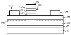
도 2는 본 발명의 일 실시예에 따른 고 전자 이동도 트랜지스터의 단면을 도시한 다른 일 단면도이다.
Claims (7)
- 제1 III-V족 반도체;
상기 제1 III-V족 반도체상 접하여 위치하는 제2 III-V족 반도체;
상기 제2 III-V족 반도체상 접하여 위치하는 게이트 절연체;
게이트 절연체 상 위치하는 게이트 전극; 및
상기 제2 III-V족 반도체상 위치하며, 상기 게이트 절연체를 사이에 두고 서로 이격 대향하는 소스 전극 및 드레인 전극;을 포함하며,
상기 게이트 절연체는 p형 금속산화물, 인트린직(intrinsic) 금속산화물 및 n형 금속산화물이 순차적으로 적층된 p-i-n 구조의 적층체를 포함하는 고 전자 이동도 트랜지스터. - 제 1항에 있어서,
상기 게이트 절연체의 p형 금속산화물은 p형 도펀트로 도핑된 상기 인트린직 금속산화물의 금속산화물이며, 상기 n형 금속산화물은 n형 도펀트로 도핑된 상기 인트린직 금속산화물인 고 전자 이동도 트랜지스터. - 제 2항에 있어서,
상기 게이트 절연체는 p형 ZnO, 인트린직 ZnO 및 n형 ZnO의 적층체를 포함하는 고 전자 이동도 트랜지스터. - 제 3항에 있어서,
상기 p형 ZnO의 p형 도펀트는 Sb, P, As 및 N에서 하나 또는 둘 이상 선택되는 원소이며, 상기 n형 ZnO의 n형 도펀트는 Ga, Al 및 In에서 하나 또는 둘 이상 선택되는 원소인 고 전자 이동도 트랜지스터. - 제 1항에 있어서,
상기 게이트 전극의 전극물질은 상기 n형 금속산화물과 오믹 접촉(Ohmic contact)하는 금속인 고 전자 이동도 트랜지스터. - 제 1항에 있어서,
상기 제1 III-V족 반도체 및 제2 III-V족 반도체는 각각 질화물 반도체인 고 전자 이동도 트랜지스터. - 제 1항에 있어서,
상기 제1 III-V족 반도체는 GaN이며, 상기 제2 III-V족 반도체는 AlGaN인 고전자 이동도 트랜지스터.
Priority Applications (1)
| Application Number | Priority Date | Filing Date | Title |
|---|---|---|---|
| KR1020170033563A KR101935928B1 (ko) | 2017-03-17 | 2017-03-17 | 게이트 누설 전류가 감소된 고 전자 이동도 트랜지스터 |
Applications Claiming Priority (1)
| Application Number | Priority Date | Filing Date | Title |
|---|---|---|---|
| KR1020170033563A KR101935928B1 (ko) | 2017-03-17 | 2017-03-17 | 게이트 누설 전류가 감소된 고 전자 이동도 트랜지스터 |
Publications (2)
| Publication Number | Publication Date |
|---|---|
| KR20180106026A true KR20180106026A (ko) | 2018-10-01 |
| KR101935928B1 KR101935928B1 (ko) | 2019-01-07 |
Family
ID=63877179
Family Applications (1)
| Application Number | Title | Priority Date | Filing Date |
|---|---|---|---|
| KR1020170033563A Expired - Fee Related KR101935928B1 (ko) | 2017-03-17 | 2017-03-17 | 게이트 누설 전류가 감소된 고 전자 이동도 트랜지스터 |
Country Status (1)
| Country | Link |
|---|---|
| KR (1) | KR101935928B1 (ko) |
Cited By (2)
| Publication number | Priority date | Publication date | Assignee | Title |
|---|---|---|---|---|
| CN111863951A (zh) * | 2020-07-28 | 2020-10-30 | 西安电子科技大学 | 增强型复合栅晶体管及其制作方法 |
| US20230352574A1 (en) * | 2022-04-29 | 2023-11-02 | Unikorn Semiconductor Corporation | Enhancement mode high-electron-mobility transistor having n-i-p semiconductor junction structure and applications thereof |
Family Cites Families (2)
| Publication number | Priority date | Publication date | Assignee | Title |
|---|---|---|---|---|
| KR101306591B1 (ko) * | 2012-06-28 | 2013-09-11 | 순천대학교 산학협력단 | 고-전자 이동도 트랜지스터 소자 및 그 제조 방법 |
| JP2017022288A (ja) * | 2015-07-13 | 2017-01-26 | 株式会社豊田中央研究所 | 半導体装置 |
-
2017
- 2017-03-17 KR KR1020170033563A patent/KR101935928B1/ko not_active Expired - Fee Related
Cited By (2)
| Publication number | Priority date | Publication date | Assignee | Title |
|---|---|---|---|---|
| CN111863951A (zh) * | 2020-07-28 | 2020-10-30 | 西安电子科技大学 | 增强型复合栅晶体管及其制作方法 |
| US20230352574A1 (en) * | 2022-04-29 | 2023-11-02 | Unikorn Semiconductor Corporation | Enhancement mode high-electron-mobility transistor having n-i-p semiconductor junction structure and applications thereof |
Also Published As
| Publication number | Publication date |
|---|---|
| KR101935928B1 (ko) | 2019-01-07 |
Similar Documents
| Publication | Publication Date | Title |
|---|---|---|
| US8907349B2 (en) | Semiconductor device and method of manufacturing the same | |
| US7956383B2 (en) | Field effect transistor | |
| TWI429076B (zh) | 二元第iii族-氮化物基高電子移動性電晶體及其製造方法 | |
| EP2747145B1 (en) | Field-effect transistor | |
| US11316039B2 (en) | Method for manufacturing semiconductor device | |
| US9219136B2 (en) | Switching element | |
| JPWO2009110254A1 (ja) | 電界効果トランジスタ及びその製造方法 | |
| CN104704608A (zh) | 氮化物半导体结构物 | |
| KR20150084855A (ko) | 이중 금속의 부분 리세스된 전극을 갖는 GaN계 쇼트키 다이오드 | |
| JP2011238805A (ja) | 電界効果トランジスタ、電界効果トランジスタの製造方法および電子装置 | |
| US20220376074A1 (en) | Nitride-based semiconductor device and method for manufacturing the same | |
| JP2010171416A (ja) | 半導体装置、半導体装置の製造方法および半導体装置のリーク電流低減方法 | |
| US12266696B2 (en) | Manufacturing method of semiconductor device | |
| US12289899B2 (en) | Nitride-based semiconductor device and method for manufacturing the same | |
| KR101935928B1 (ko) | 게이트 누설 전류가 감소된 고 전자 이동도 트랜지스터 | |
| US11935947B2 (en) | Enhancement mode high electron mobility transistor | |
| CN114141870A (zh) | 一种可靠性增强的iii族氮化物半导体高电子迁移率晶体管及其制造方法 | |
| US20220005939A1 (en) | Semiconductor device and fabrication method thereof | |
| US11721751B2 (en) | HEMT and method of fabricating the same | |
| TW202345402A (zh) | 半導體裝置 | |
| US20160211335A1 (en) | Semiconductor device | |
| TWI916096B (zh) | 半導體裝置 | |
| WO2024011609A1 (en) | Semiconductor device and method for manufacturing thereof | |
| WO2024040465A1 (en) | Nitride-based semiconductor device and method for manufacturing the same | |
| WO2024060110A1 (en) | Nitride-based semiconductor device and method for manufacturing thereof |
Legal Events
| Date | Code | Title | Description |
|---|---|---|---|
| A201 | Request for examination | ||
| PA0109 | Patent application |
St.27 status event code: A-0-1-A10-A12-nap-PA0109 |
|
| PA0201 | Request for examination |
St.27 status event code: A-1-2-D10-D11-exm-PA0201 |
|
| D13-X000 | Search requested |
St.27 status event code: A-1-2-D10-D13-srh-X000 |
|
| D14-X000 | Search report completed |
St.27 status event code: A-1-2-D10-D14-srh-X000 |
|
| E902 | Notification of reason for refusal | ||
| PE0902 | Notice of grounds for rejection |
St.27 status event code: A-1-2-D10-D21-exm-PE0902 |
|
| T11-X000 | Administrative time limit extension requested |
St.27 status event code: U-3-3-T10-T11-oth-X000 |
|
| E13-X000 | Pre-grant limitation requested |
St.27 status event code: A-2-3-E10-E13-lim-X000 |
|
| P11-X000 | Amendment of application requested |
St.27 status event code: A-2-2-P10-P11-nap-X000 |
|
| P13-X000 | Application amended |
St.27 status event code: A-2-2-P10-P13-nap-X000 |
|
| PG1501 | Laying open of application |
St.27 status event code: A-1-1-Q10-Q12-nap-PG1501 |
|
| E701 | Decision to grant or registration of patent right | ||
| PE0701 | Decision of registration |
St.27 status event code: A-1-2-D10-D22-exm-PE0701 |
|
| GRNT | Written decision to grant | ||
| PR0701 | Registration of establishment |
St.27 status event code: A-2-4-F10-F11-exm-PR0701 |
|
| PR1002 | Payment of registration fee |
St.27 status event code: A-2-2-U10-U11-oth-PR1002 Fee payment year number: 1 |
|
| PG1601 | Publication of registration |
St.27 status event code: A-4-4-Q10-Q13-nap-PG1601 |
|
| R18-X000 | Changes to party contact information recorded |
St.27 status event code: A-5-5-R10-R18-oth-X000 |
|
| PN2301 | Change of applicant |
St.27 status event code: A-5-5-R10-R13-asn-PN2301 St.27 status event code: A-5-5-R10-R11-asn-PN2301 |
|
| R18-X000 | Changes to party contact information recorded |
St.27 status event code: A-5-5-R10-R18-oth-X000 |
|
| PN2301 | Change of applicant |
St.27 status event code: A-5-5-R10-R13-asn-PN2301 St.27 status event code: A-5-5-R10-R11-asn-PN2301 |
|
| PN2301 | Change of applicant |
St.27 status event code: A-5-5-R10-R13-asn-PN2301 St.27 status event code: A-5-5-R10-R11-asn-PN2301 |
|
| PR1001 | Payment of annual fee |
St.27 status event code: A-4-4-U10-U11-oth-PR1001 Fee payment year number: 4 |
|
| PR1001 | Payment of annual fee |
St.27 status event code: A-4-4-U10-U11-oth-PR1001 Fee payment year number: 5 |
|
| R18-X000 | Changes to party contact information recorded |
St.27 status event code: A-5-5-R10-R18-oth-X000 |
|
| R18-X000 | Changes to party contact information recorded |
St.27 status event code: A-5-5-R10-R18-oth-X000 |
|
| PC1903 | Unpaid annual fee |
St.27 status event code: A-4-4-U10-U13-oth-PC1903 Not in force date: 20240101 Payment event data comment text: Termination Category : DEFAULT_OF_REGISTRATION_FEE |
|
| PC1903 | Unpaid annual fee |
St.27 status event code: N-4-6-H10-H13-oth-PC1903 Ip right cessation event data comment text: Termination Category : DEFAULT_OF_REGISTRATION_FEE Not in force date: 20240101 |
|
| P22-X000 | Classification modified |
St.27 status event code: A-4-4-P10-P22-nap-X000 |