KR20180062222A - Organic Light Emitting Device and Organic Light Emitting Display Apparatus using the same - Google Patents
Organic Light Emitting Device and Organic Light Emitting Display Apparatus using the same Download PDFInfo
- Publication number
- KR20180062222A KR20180062222A KR1020160162259A KR20160162259A KR20180062222A KR 20180062222 A KR20180062222 A KR 20180062222A KR 1020160162259 A KR1020160162259 A KR 1020160162259A KR 20160162259 A KR20160162259 A KR 20160162259A KR 20180062222 A KR20180062222 A KR 20180062222A
- Authority
- KR
- South Korea
- Prior art keywords
- layer
- stack
- light emitting
- emission
- organic light
- Prior art date
- Legal status (The legal status is an assumption and is not a legal conclusion. Google has not performed a legal analysis and makes no representation as to the accuracy of the status listed.)
- Granted
Links
Images






Classifications
-
- H01L51/5278—
-
- H—ELECTRICITY
- H10—SEMICONDUCTOR DEVICES; ELECTRIC SOLID-STATE DEVICES NOT OTHERWISE PROVIDED FOR
- H10K—ORGANIC ELECTRIC SOLID-STATE DEVICES
- H10K50/00—Organic light-emitting devices
- H10K50/10—OLEDs or polymer light-emitting diodes [PLED]
- H10K50/19—Tandem OLEDs
-
- H01L27/3209—
-
- H01L27/3262—
-
- H01L51/504—
-
- H01L51/5048—
-
- H01L51/5056—
-
- H—ELECTRICITY
- H10—SEMICONDUCTOR DEVICES; ELECTRIC SOLID-STATE DEVICES NOT OTHERWISE PROVIDED FOR
- H10K—ORGANIC ELECTRIC SOLID-STATE DEVICES
- H10K50/00—Organic light-emitting devices
- H10K50/10—OLEDs or polymer light-emitting diodes [PLED]
- H10K50/11—OLEDs or polymer light-emitting diodes [PLED] characterised by the electroluminescent [EL] layers
- H10K50/125—OLEDs or polymer light-emitting diodes [PLED] characterised by the electroluminescent [EL] layers specially adapted for multicolour light emission, e.g. for emitting white light
- H10K50/13—OLEDs or polymer light-emitting diodes [PLED] characterised by the electroluminescent [EL] layers specially adapted for multicolour light emission, e.g. for emitting white light comprising stacked EL layers within one EL unit
-
- H—ELECTRICITY
- H10—SEMICONDUCTOR DEVICES; ELECTRIC SOLID-STATE DEVICES NOT OTHERWISE PROVIDED FOR
- H10K—ORGANIC ELECTRIC SOLID-STATE DEVICES
- H10K50/00—Organic light-emitting devices
- H10K50/10—OLEDs or polymer light-emitting diodes [PLED]
- H10K50/14—Carrier transporting layers
-
- H—ELECTRICITY
- H10—SEMICONDUCTOR DEVICES; ELECTRIC SOLID-STATE DEVICES NOT OTHERWISE PROVIDED FOR
- H10K—ORGANIC ELECTRIC SOLID-STATE DEVICES
- H10K50/00—Organic light-emitting devices
- H10K50/10—OLEDs or polymer light-emitting diodes [PLED]
- H10K50/14—Carrier transporting layers
- H10K50/15—Hole transporting layers
-
- H—ELECTRICITY
- H10—SEMICONDUCTOR DEVICES; ELECTRIC SOLID-STATE DEVICES NOT OTHERWISE PROVIDED FOR
- H10K—ORGANIC ELECTRIC SOLID-STATE DEVICES
- H10K59/00—Integrated devices, or assemblies of multiple devices, comprising at least one organic light-emitting element covered by group H10K50/00
- H10K59/10—OLED displays
- H10K59/12—Active-matrix OLED [AMOLED] displays
- H10K59/121—Active-matrix OLED [AMOLED] displays characterised by the geometry or disposition of pixel elements
- H10K59/1213—Active-matrix OLED [AMOLED] displays characterised by the geometry or disposition of pixel elements the pixel elements being TFTs
-
- H—ELECTRICITY
- H10—SEMICONDUCTOR DEVICES; ELECTRIC SOLID-STATE DEVICES NOT OTHERWISE PROVIDED FOR
- H10K—ORGANIC ELECTRIC SOLID-STATE DEVICES
- H10K59/00—Integrated devices, or assemblies of multiple devices, comprising at least one organic light-emitting element covered by group H10K50/00
- H10K59/30—Devices specially adapted for multicolour light emission
- H10K59/32—Stacked devices having two or more layers, each emitting at different wavelengths
-
- H01L2251/558—
-
- H—ELECTRICITY
- H10—SEMICONDUCTOR DEVICES; ELECTRIC SOLID-STATE DEVICES NOT OTHERWISE PROVIDED FOR
- H10K—ORGANIC ELECTRIC SOLID-STATE DEVICES
- H10K2102/00—Constructional details relating to the organic devices covered by this subclass
- H10K2102/301—Details of OLEDs
- H10K2102/351—Thickness
Landscapes
- Physics & Mathematics (AREA)
- Optics & Photonics (AREA)
- Geometry (AREA)
- Engineering & Computer Science (AREA)
- Microelectronics & Electronic Packaging (AREA)
- Electroluminescent Light Sources (AREA)
Abstract
본 발명은, 양극과 음극 사이에 구비된 제1 스택, 제2 스택, 및 제3 스택을 포함하여 이루어지고, 상기 제2 스택은 서로 상이한 층에 적층된 적색 발광층 및 녹색 발광층을 포함하여 이루어진 유기 발광 소자 및 그를 이용한 유기 발광 표시 장치를 제공한다. The present invention relates to an organic electroluminescent device comprising a first stack, a second stack, and a third stack provided between an anode and a cathode, wherein the second stack comprises a red light emitting layer and a green light emitting layer A light emitting device and an organic light emitting display using the same are provided.
Description
본 발명은 유기 발광 소자에 관한 것으로서, 보다 구체적으로는 백색광을 발광하는 유기 발광 소자에 관한 것이다. BACKGROUND OF THE
유기 발광 소자는 전자(electron)를 주입하는 음극(cathode)과 정공(hole)을 주입하는 양극(anode) 사이에 발광층이 형성된 구조를 가지며, 음극에서 발생된 전자 및 양극에서 발생된 정공이 발광층 내로 주입되면 주입된 전자 및 정공이 결합하여 엑시톤(exciton)이 생성되고, 생성된 엑시톤이 여기상태(excited state)에서 기저상태(ground state)로 떨어지면서 발광을 하는 원리를 이용한 소자이다. The organic light emitting device has a structure in which a light emitting layer is formed between a cathode for injecting electrons and an anode for injecting holes, and electrons generated in the cathode and holes generated in the anode are injected into the light emitting layer When excited, excited electrons and holes are coupled to generate excitons, and the generated excitons emit light while falling from the excited state to the ground state.
이와 같은 유기 발광 소자는 조명뿐만 아니라 액정표시장치의 박형 광원 또는 표시 장치 등에 다양하게 적용될 수 있는데, 특히 백색광을 발광하는 유기 발광 소자는 컬러 필터와 조합하여 풀 컬러 표시 장치에 적용될 수 있다. Such an organic light emitting device can be applied not only to illumination but also to a thin light source or a display device of a liquid crystal display device. In particular, an organic light emitting device that emits white light can be applied to a full color display device in combination with a color filter.
이하 도면을 참조로 종래의 유기 발광 소자에 대해서 설명하기로 한다. Hereinafter, a conventional organic light emitting device will be described with reference to the drawings.
도 1a는 종래의 유기 발광 소자의 개략적인 단면도이고, 도 1b는 종래의 유기 발광 소자의 발광 스펙트럼을 보여주는 그래프이다. FIG. 1A is a schematic cross-sectional view of a conventional organic light emitting device, and FIG. 1B is a graph showing an emission spectrum of a conventional organic light emitting device.
도 1a에서 알 수 있듯이, 종래의 유기 발광 소자는 양극(Anode), 제1 스택(1st Stack), 전하 생성층(Charge Generating Layer; CGL), 제2 스택(2nd Stack), 및 음극(Cathode)을 포함하여 이루어진다. 1A, a conventional organic light emitting device includes an anode, a first stack, a charge generating layer (CGL), a second stack (second stack), and a cathode. .
상기 제1 스택(1st Stack)은 상기 양극(Anode) 상에 형성되며 청색(Blue; B) 발광층(Emitting Layer; EML)을 포함하여 이루어진다. The first stack is formed on the anode and includes a blue (B) emission layer (EML).
상기 전하 생성층(CGL)은 상기 제1 스택(1st Stack)과 상기 제2 스택(2nd Stack) 사이에 형성되어 상기 제1 스택(1st Stack)과 상기 제2 스택(2nd Stack) 사이에서 전하를 균형되게 조절한다. The charge generation layer CGL may be formed between the first stack and the second stack so that charge is generated between the first stack and the second stack Balanced control.
상기 제2 스택(2nd Stack)은 상기 전하 생성층(CGL)과 상기 음극(Cathode) 사이에 형성되며 황녹색(Yellow Green; YG) 발광층(Emitting Layer; EML)을 포함하여 이루어진다. The second stack (2nd Stack) is formed between the charge generation layer (CGL) and the cathode and includes a yellow green (YG) emission layer (EML).
이와 같은 종래의 유기 발광 소자의 경우, 상기 제1 스택(1st Stack)의 청색(B) 발광층(EML)에서 발광된 청색의 광과 상기 제2 스택(2nd Stack)의 황녹색(YG) 발광층(EML)에서 발광된 황녹색 광이 혼합되어 백색(White)의 광을 방출한다. In such a conventional organic light emitting device, the blue light emitted from the blue (B) emission layer (EML) of the first stack and the yellow (YG) emission layer of the second stack EML) is mixed to emit white light.
그러나, 종래의 유기 발광 소자는 2 개의 피크 파장을 가지는 발광 스펙트럼을 보임으로써 화상을 표시할 때 색재현율이 떨어지는 단점이 있다. However, the conventional organic light emitting device has a disadvantage that the color reproduction rate is low when an image is displayed by displaying an emission spectrum having two peak wavelengths.
즉, 도 1b에서 알 수 있듯이, 종래의 경우, 상기 제1 스택(1st Stack)에서 방출되는 청색(B) 광에 의해서 단파장 대역에서 하나의 피크 파장이 나타나고 상기 제2 스택(2nd Stack)에서 방출되는 황녹색(YG) 광에 의해서 장파장 대역에서 하나의 피크 파장이 나타난다. 이와 같이 장파장 대역에서 하나의 피크 파장만이 나타남으로써 구현할 수 있는 색상 범위가 한정되고 따라서 색재현율이 떨어지는 단점이 있다. 특히, 종래의 경우 상기 제2 스택(2nd Stack)의 황녹색(YG) 발광층(EML)을 통해서 녹색(G)과 적색(R)을 구현하게 되는데, 이 경우 적색(R)의 광효율이 낮은 문제가 있다. 1B, in the conventional case, one peak wavelength appears in the short wavelength band due to the blue (B) light emitted from the first stack and is emitted from the second stack (second stack) A single peak wavelength appears in the long wavelength band by the yellow green (YG) light. As described above, only one peak wavelength appears in the long wavelength band, which limits the color range that can be implemented and thus the color reproduction rate is deteriorated. Particularly, in the conventional case, green (G) and red (R) are realized through the yellow green (YG) emission layer (EML) of the second stack (2nd Stack). In this case, .
본 발명자는 색재현율이 떨어지는 종래의 문제점을 해결하기 위해서 전술한 도 1a의 구조에서 제2 스택(2nd Stack)에 황녹색(YG) 발광층(EML)과 더불어 적색(R) 발광층을 추가로 형성한 유기 발광 소자에 대해서 테스트하였다. In order to solve the conventional problem of low color reproducibility, the inventors of the present invention have found that a red (R) emission layer is formed in addition to a yellow (YG) emission layer (EML) in a second stack The organic light emitting device was tested.
그 결과, 얻어진 유기 발광 소자가 단파장 대역에서 하나의 피크 파장을 나타내고 장파장 대역에서 두 개의 피크 파장을 나타내게 되어 결국 세 개의 피크 파장을 가지게 되고 또한 적색(R)의 광효율도 향상됨을 확인하였다. As a result, it was confirmed that the obtained organic light emitting device exhibited one peak wavelength in a short wavelength band and two peak wavelengths in a long wavelength band, resulting in three peak wavelengths, and also a light efficiency of red (R).
그러나, 제2 스택(2nd Stack)에 황녹색(YG) 발광층(EML)과 적색(R) 발광층이 함께 포함될 경우 녹색(G)의 광효율이 떨어지는 문제가 발생하였고, 그로 인해서 색재현율이 개선되지 않음을 확인하였다. However, when the yellow (YG) emission layer (EML) and the red (R) emission layer are included in the second stack (2nd Stack), the light efficiency of green (G) is lowered, Respectively.
따라서, 본 발명은 적색(R)과 녹색(G)의 발광 효율을 모두 향상시킴으로써 색재현율이 향상될 수 있는 유기 발광 소자 및 그를 이용한 유기 발광 표시 장치를 제공하는 것을 목적으로 한다. Accordingly, it is an object of the present invention to provide an organic light emitting device capable of improving the color reproduction ratio by improving both the red (R) and green (G) luminous efficiency, and an organic light emitting display using the same.
본 발명은 상기 목적을 달성하기 위해서, 양극과 음극 사이에 구비된 제1 스택, 제2 스택, 및 제3 스택을 포함하여 이루어지고, 상기 제2 스택은 서로 상이한 층에 적층된 적색 발광층 및 녹색 발광층을 포함하여 이루어진 유기 발광 소자를 제공한다. In order to achieve the above object, the present invention provides a light emitting device comprising a first stack, a second stack, and a third stack provided between an anode and a cathode, the second stack comprising a red light emitting layer and a green An organic light emitting device comprising a light emitting layer is provided.
본 발명은 또한 기판 상에 구비된 박막 트랜지스터층, 및 상기 박막 트랜지스터층 상에 구비된 유기 발광 소자를 포함하고, 상기 유기 발광 소자는 양극과 음극 사이에 구비된 제1 스택, 제2 스택, 및 제3 스택을 포함하여 이루어지고, 상기 제2 스택은 서로 상이한 층에 적층된 적색 발광층 및 녹색 발광층을 포함하여 이루어진 유기 발광 표시 장치를 제공한다. The present invention also includes a thin film transistor layer provided on a substrate, and an organic light emitting element provided on the thin film transistor layer, wherein the organic light emitting element includes a first stack, a second stack, And a third stack, wherein the second stack includes a red light emitting layer and a green light emitting layer stacked in layers different from each other.
본 발명에 따르면 다음과 같은 효과가 있다. The present invention has the following effects.
본 발명의 일 실시예에 따르면, 제1 스택과 제2 스택 사이에 구비되는 제2 스택이 적색(R) 발광층(EML) 및 녹색(G) 발광층(EML)을 포함하고 있기 때문에, 적색(R)과 녹색(G)의 발광 효율을 모두 향상시킴으로써 색재현율이 향상될 수 있다. According to an embodiment of the present invention, since the second stack provided between the first stack and the second stack includes a red (R) emission layer (EML) and a green (G) emission layer (EML) ) And green (G), the color reproduction rate can be improved.
본 발명의 다른 실시예에 따르면, 제2스택이 적색(R) 발광층(EML)과 녹색(G) 발광층(EML) 사이에 발광 조절층(ECL)을 추가로 포함함으로써, 시야각에 따른 색상 변화가 줄어들어 색시야각 특성이 향상될 수 있다. According to another embodiment of the present invention, the second stack further includes an emission control layer (ECL) between the red (R) emission layer (EML) and the green (G) emission layer (EML) The color viewing angle characteristics can be improved.
도 1a는 종래의 유기 발광 소자의 개략적인 단면도이고, 도 1b는 종래의 유기 발광 소자의 발광 스펙트럼을 보여주는 그래프이다.
도 2는 본 발명의 일 실시예에 따른 유기 발광 소자의 개략적인 단면도이다.
도 3은 본 발명의 다른 실시예에 따른 유기 발광 소자의 개략적인 단면도이다.
도 4는 본 발명의 실시예 1과 실시예 2에 따른 유기 발광 소자의 파장대별 발광세기를 보여주는 그래프이다.
도 5는 본 발명의 실시예 1과 실시예 2에 따른 유기 발광 소자의 시야각에 따른 색변화율을 보여주는 그래프이다.
도 6은 다양한 조성을 가지는 발광 조절층을 적용함에 따른 파장대별 발광세기 변화를 보여주는 그래프이다.
도 7은 발광 조절층(ECL)의 두께 변화에 따른 색시야각 특성 변화를 보여주는 그래프이다.
도 8은 비교예, 실시예 1, 및 실시예 2에 따른 유기 발광 소자의 파장대별 발광 세기를 보여주는 그래프이다.
도 9는 비교예, 실시예 1, 및 실시예 2에 따른 유기 발광 소자의 색 영역을 보여주는 그래프이다.
도 10은 비교예, 실시예 1, 및 실시예 2에 따른 유기 발광 소자의 시야각에 따른 색변화율을 보여주는 그래프이다.FIG. 1A is a schematic cross-sectional view of a conventional organic light emitting device, and FIG. 1B is a graph showing an emission spectrum of a conventional organic light emitting device.
2 is a schematic cross-sectional view of an organic light emitting device according to an embodiment of the present invention.
3 is a schematic cross-sectional view of an organic light emitting device according to another embodiment of the present invention.
4 is a graph showing the intensity of light emitted by the organic light emitting device according to Example 1 and Example 2 of the present invention.
5 is a graph showing a color change ratio according to viewing angles of organic light emitting devices according to Example 1 and Example 2 of the present invention.
FIG. 6 is a graph showing a change in luminescence intensity by wavelength band as a result of application of the emission control layer having various compositions.
7 is a graph showing changes in color viewing angle characteristics according to the thickness of the emission control layer (ECL).
FIG. 8 is a graph showing luminescence intensities of the organic luminescent devices according to Comparative Examples, Examples 1 and 2 according to wavelengths.
FIG. 9 is a graph showing the color gamut of the organic luminescent device according to the comparative example, the first embodiment, and the second embodiment.
10 is a graph showing the rate of change of color according to viewing angles of organic light emitting devices according to Comparative Examples, Examples 1 and 2.
본 발명의 이점 및 특징, 그리고 그것들을 달성하는 방법은 첨부되는 도면과 함께 상세하게 후술되어 있는 실시예들을 참조하면 명확해질 것이다. 그러나 본 발명은 이하에서 개시되는 실시예들에 한정되는 것이 아니라 서로 다른 다양한 형태로 구현될 것이며, 단지 본 실시예들은 본 발명의 개시가 완전하도록 하며, 본 발명이 속하는 기술 분야에서 통상의 지식을 가진 자에게 발명의 범주를 완전하게 알려주기 위해 제공되는 것이며, 본 발명은 청구항의 범주에 의해 정의될 뿐이다. BRIEF DESCRIPTION OF THE DRAWINGS The advantages and features of the present invention, and the manner of achieving them, will be apparent from and elucidated with reference to the embodiments described hereinafter in conjunction with the accompanying drawings. The present invention may, however, be embodied in many different forms and should not be construed as being limited to the embodiments set forth herein. Rather, these embodiments are provided so that this disclosure will be thorough and complete, and will fully convey the scope of the invention to those skilled in the art. Is provided to fully convey the scope of the invention to those skilled in the art, and the invention is only defined by the scope of the claims.
본 발명의 실시예를 설명하기 위한 도면에 개시된 형상, 크기, 비율, 각도, 개수 등은 예시적인 것이므로 본 발명이 도시된 사항에 한정되는 것은 아니다. 명세서 전체에 걸쳐 동일 참조 부호는 동일 구성 요소를 지칭한다. 또한, 본 발명을 설명함에 있어서, 관련된 공지 기술에 대한 구체적인 설명이 본 발명의 요지를 불필요하게 흐릴 수 있다고 판단되는 경우 그 상세한 설명은 생략한다. 본 명세서 상에서 언급한 '포함한다', '갖는다', '이루어진다' 등이 사용되는 경우 '~만'이 사용되지 않는 이상 다른 부분이 추가될 수 있다. 구성 요소를 단수로 표현한 경우에 특별히 명시적인 기재 사항이 없는 한 복수를 포함하는 경우를 포함한다.The shapes, sizes, ratios, angles, numbers, and the like disclosed in the drawings for describing the embodiments of the present invention are illustrative, and thus the present invention is not limited thereto. Like reference numerals refer to like elements throughout the specification. In the following description, well-known functions or constructions are not described in detail since they would obscure the invention in unnecessary detail. In the case where the word 'includes', 'having', 'done', etc. are used in this specification, other parts can be added unless '~ only' is used. Unless the context clearly dictates otherwise, including the plural unless the context clearly dictates otherwise.
구성 요소를 해석함에 있어서, 별도의 명시적 기재가 없더라도 오차 범위를 포함하는 것으로 해석한다.In interpreting the constituent elements, it is construed to include the error range even if there is no separate description.
위치 관계에 대한 설명일 경우, 예를 들어, '~상에', '~상부에', '~하부에', '~옆에' 등으로 두 부분의 위치 관계가 설명되는 경우, '바로' 또는 '직접'이 사용되지 않는 이상 두 부분 사이에 하나 이상의 다른 부분이 위치할 수도 있다.In the case of a description of the positional relationship, for example, if the positional relationship between two parts is described as 'on', 'on top', 'under', and 'next to' Or " direct " is not used, one or more other portions may be located between the two portions.
시간 관계에 대한 설명일 경우, 예를 들어, '~후에', '~에 이어서', '~다음에', '~전에' 등으로 시간적 선후 관계가 설명되는 경우, '바로' 또는 '직접'이 사용되지 않는 이상 연속적이지 않은 경우도 포함할 수 있다.In the case of a description of a temporal relationship, for example, if the temporal relationship is described by 'after', 'after', 'after', 'before', etc., May not be continuous unless they are not used.
제1, 제2 등이 다양한 구성요소들을 서술하기 위해서 사용되나, 이들 구성요소들은 이들 용어에 의해 제한되지 않는다. 이들 용어들은 단지 하나의 구성 요소를 다른 구성요소와 구별하기 위하여 사용하는 것이다. 따라서, 이하에서 언급되는 제1 구성요소는 본 발명의 기술적 사상 내에서 제2 구성요소일 수도 있다.The first, second, etc. are used to describe various components, but these components are not limited by these terms. These terms are used only to distinguish one component from another. Therefore, the first component mentioned below may be the second component within the technical spirit of the present invention.
본 발명의 여러 실시예들의 각각 특징들이 부분적으로 또는 전체적으로 서로 결합 또는 조합 가능하고, 기술적으로 다양한 연동 및 구동이 가능하며, 각 실시예들이 서로에 대하여 독립적으로 실시 가능할 수도 있고 연관 관계로 함께 실시할 수도 있다. It is to be understood that each of the features of the various embodiments of the present invention may be combined or combined with each other, partially or wholly, technically various interlocking and driving, and that the embodiments may be practiced independently of each other, It is possible.
이하, 도면을 참조로 본 발명의 바람직한 실시예에 대해서 상세히 설명하기로 한다. Hereinafter, preferred embodiments of the present invention will be described in detail with reference to the drawings.
도 2는 본 발명의 일 실시예에 따른 유기 발광 소자의 개략적인 단면도이다. 2 is a schematic cross-sectional view of an organic light emitting device according to an embodiment of the present invention.
도 2에서 알 수 있듯이, 본 발명의 일 실시예에 따른 유기 발광 소자는 양극(Anode), 제1 스택(1st Stack), 제1 전하 생성층(1st CGL), 제2 스택(2nd Stack), 제2 전하 생성층(2nd CGL), 제3 스택(3rd Stack), 및 음극(Cathode)을 포함하여 이루어진다. 2, an organic light emitting diode according to an exemplary embodiment of the present invention includes an anode, a first stack, a first charge generating layer (first CGL), a second stack (second stack) A second charge generating layer (2nd CGL), a third stack (third stack), and a cathode.
상기 양극(Anode)은 일함수(work function)가 높은 투명 도전층을 포함하여 이루어질 수 있다. 상기 투명 도전층은 ITO(Indium Tin Oxide), IZO(Indium Zinc Oxide), SnO2 또는 ZnO 등으로 이루어질 수 있지만, 반드시 그에 한정되는 것은 아니다. The anode may include a transparent conductive layer having a high work function. The transparent conductive layer may be formed of ITO (Indium Tin Oxide), IZO (indium zinc oxide), SnO 2 or ZnO, but is not limited thereto.
상기 제1 스택(1st Stack)은 상기 양극(Anode) 상에 형성되어 청색(B) 광을 발광한다. 이와 같은 제1 스택(1st Stack)은 정공 주입층(Hole Injecting Layer; HIL), 제1 정공 수송층(1st Hole Transporting Layer; 1st HTL), 제1 발광층(1st Emitting Layer; 1st EML), 및 제1 전자 수송층(1st Electron Transporting Layer; 1st ETL)을 포함하여 이루어진다. The first stack (Stack) is formed on the anode to emit blue (B) light. The first stack may include a hole injection layer (HIL), a first hole transporting layer (HTL), a first emission layer (EML), and a first hole transport layer And a first electron transport layer (1st ETL).
상기 정공 주입층(HIL)은 상기 양극(Anode) 상에 형성되며, MTDATA(4,4',4"-tris(3-methylphenylphenylamino)triphenylamine), CuPc(copper phthalocyanine) 또는 PEDOT/PSS(poly(3,4-ethylenedioxythiphene, polystyrene sulfonate) 등으로 이루어질 수 있지만, 반드시 그에 한정되는 것은 아니다. 상기 정공 주입층(HIL)은 상기 제1 정공 수송층(1st HTL)을 구성하는 물질에 P타입의 도펀트가 도핑되어 이루어질 수도 있다. The hole injecting layer HIL is formed on the anode and may be formed of MTDATA (4,4 ', 4 "-tris (3-methylphenylphenylamino) triphenylamine), CuPc (copper phthalocyanine) or PEDOT / PSS , 4-ethylenedioxythiophene, and polystyrene sulfonate). However, the present invention is not limited thereto. The hole injection layer (HIL) may be formed by doping a P-type dopant into the first hole transport layer .
상기 제1 정공 수송층(1st HTL)은 상기 정공 주입층(HIL) 상에 형성되며, TPD(N,N'-diphenyl-N,N'-bis(3-methylphenyl)-1,1'-bi-phenyl-4,4'-diamine), NPD(N, N-dinaphthyl-N, N’-diphenyl benzidine), 또는 NPB(N,N'-di(naphthalen-1-yl)-N,N'-diphenyl-benzidine) 등으로 이루어질 수 있지만, 반드시 그에 한정되는 것은 아니다. 상기 제1 정공 수송층(1st HTL)은 P타입의 도펀트가 포함되지 않은 것을 제외하고 상기 정공 주입층(HIL)과 동일한 물질로 이루어질 수 있으며, 이 경우 동일한 공정 장비에서 연속 증착 공정으로 상기 정공 주입층(HIL)과 제1 정공 수송층(1st HTL)을 형성할 수 있다. The first HTL may be formed on the hole injection layer (HIL), and may be TPD (N, N'-diphenyl-N, N'-bis (3-methylphenyl) phenyl-4,4'-diamine, NPD (N, N-diphenyl benzidine), or NPB (N, N'- -benzidine), and the like, but the present invention is not limited thereto. The first HTL may be formed of the same material as that of the HIL except that the P type dopant is not included. In this case, in the same process equipment, (HIL) and a first hole transport layer (1st HTL).
상기 제1 발광층(1st EML)은 상기 제1 정공 수송층(1st HTL) 상에 형성된다. 상기 제1 발광층(1st EML)은 청색(B) 광을 발광하는 청색 발광층으로 이루어진다. The first emission layer (1st EML) is formed on the first HTL (1st HTL). The first emission layer (1st EML) is composed of a blue emission layer that emits blue (B) light.
상기 제1 발광층(1st EML)은 청색(B) 광, 예를 들어 피크(peak) 파장 범위가 440nm 내지 480nm 범위의 청색 광을 발광할 수 있는 유기물질을 포함할 수 있으며, 구체적으로, 안트라센(anthracene) 유도체, 파이렌(pyrene) 유도체 및 페릴렌(perylene) 유도체로 이루어진 그룹에서 선택된 적어도 하나의 호스트 물질에 청색 도펀트가 도핑되어 이루어질 수 있지만, 반드시 그에 한정되는 것은 아니다. The first EML may include an organic material capable of emitting blue light, for example, a blue light having a peak wavelength in the range of 440 nm to 480 nm, and specifically, an anthracene an anthracene derivative, a pyrene derivative, and a perylene derivative may be doped with at least one host material, but the present invention is not limited thereto.
상기 제1 전자 수송층(1st ETL)은 상기 제1 발광층(1st EML) 상에 형성되며, 카바졸(carbazole), 옥사디아졸(oxadiazole), 트리아졸(triazole), 페난트롤린(phenanthroline), 벤족사졸(benzoxazole) 또는 벤즈티아졸(benzthiazole) 등으로 이루어질 수 있지만, 반드시 그에 한정되는 것은 아니다.The first electron transport layer (1st ETL) is formed on the first emission layer (1st EML), and includes carbazole, oxadiazole, triazole, phenanthroline, Benzoxazole, benzthiazole, and the like, but the present invention is not limited thereto.
상기 제1 전하 생성층(1st CGL)은 상기 제1 스택(1st Stack)과 상기 제2 스택(2nd Stack) 사이에 형성되어 상기 제1 스택(1st Stack)과 상기 제2 스택(2nd Stack) 사이에서 전하를 균형되게 조절하는 역할을 한다. The first charge generation layer (1st CGL) is formed between the first stack and the second stack and is disposed between the first stack and the second stack The charge is controlled in a balanced manner.
상기 제1 전하 생성층(1st CGL)은 상기 제1 스택(1st Stack) 상에 형성되며 상기 제1 스택(1st Stack)에 인접하게 위치하는 N형 전하 생성층 및 상기 N형 전하 생성층 상에 형성되며 상기 제2 스택(2nd Stack)에 인접하게 위치하는 P형 전하 생성층을 포함하여 이루어질 수 있다. The first charge generation layer (1st CGL) includes an N-type charge generation layer formed on the first stack and positioned adjacent to the first stack, and an N-type charge generation layer formed on the N-type charge generation layer And a P-type charge generation layer formed adjacent to the second stack (second stack).
상기 N형 전하 생성층은 상기 제1 스택(1st Stack)으로 전자(electron)를 주입해주고, 상기 P형 전하 생성층은 상기 제2 스택(2nd Stack)으로 정공(hole)을 주입해준다. 상기 N형 전하 생성층은 Li, Na, K, 또는 Cs와 같은 알칼리 금속, 또는 Mg, Sr, Ba, 또는 Ra와 같은 알칼리 토금속으로 도핑된 유기층으로 이루어질 수 있다. 상기 P형 전하 생성층은 정공수송능력이 있는 유기물질에 도펀트가 도핑되어 이루어질 수 있다. The N-type charge generation layer injects electrons into the first stack, and the P-type charge generation layer injects holes into the second stack. The N-type charge generation layer may be composed of an organic layer doped with an alkali metal such as Li, Na, K, or Cs, or an alkaline earth metal such as Mg, Sr, Ba, or Ra. The P-type charge generation layer may be doped with an organic material having a hole transporting ability.
상기 제2 스택(2nd Stack)은 상기 제1 전하 생성층(1st CGL) 상에 형성되어 적색(Red; R) 광 및 녹색(Green; G) 광을 발광할 수 있다. The second stack may be formed on the first charge generation layer (1st CGL) to emit red (R) light and green (G) light.
이와 같은 제2 스택(2nd Stack)은 제2 정공 수송층(2nd HTL), 제2 발광층(2nd EML), 제3 발광층(3rd EML), 및 제2 전자 수송층(2nd ETL)을 포함하여 이루어진다. The second stack (2nd Stack) includes a second HTL, a second EML, a third EML, and a second ETL.
상기 제2 정공 수송층(2nd HTL)은 상기 제1 전하 생성층(1st CGL) 상에 형성되며, TPD(N,N'-diphenyl-N,N'-bis(3-methylphenyl)-1,1'-bi-phenyl-4,4'-diamine), NPD(N, N-dinaphthyl-N, N’-diphenyl benzidine), 또는 NPB(N,N'-di(naphthalen-1-yl)-N,N'-diphenyl-benzidine) 등으로 이루어질 수 있지만, 반드시 그에 한정되는 것은 아니다. 상기 제2 정공 수송층(2nd HTL)은 상기 제1 정공 수송층(1st HTL)과 동일한 물질로 이루어질 수 있지만, 경우에 따라서 서로 상이한 물질로 이루어질 수도 있다. The second hole transport layer (2nd HTL) is formed on the first charge generation layer (1st CGL), and TPD (N, N'-diphenyl-N, N'- -bi-phenyl-4,4'-diamine, NPD (N-dinaphthyl-N, N'-diphenyl benzidine), or NPB (naphthalen- '-diphenyl-benzidine), and the like, but the present invention is not limited thereto. The second HTL may be made of the same material as the first HTL, but may be made of a material different from the first HTL.
상기 제2 발광층(2nd EML)은 상기 제2 정공 수송층(2nd HTL) 상에 형성된다. The second emission layer (2nd EML) is formed on the second HTL (2nd HTL).
상기 제2 발광층(2nd EML)은 적색(R) 광, 예를 들어 피크 파장 범위가 600nm 내지 650nm 범위의 광을 발광하는 유기물질을 포함할 수 있으며, 구체적으로 카바졸계 화합물 또는 금속 착물로 이루어진 호스트 물질에 적색의 도펀트가 도핑되어 이루어질 수 있다. 상기 카바졸계 화합물은 CBP(4,4-N,N'-dicarbazole-biphenyl), CBP 유도체, mCP(N,N'-dicarbazolyl-3,5-benzene) 또는 mCP 유도체 등을 포함할 수 있고, 상기 금속 착물은 ZnPBO(phenyloxazole) 금속 착물 또는 ZnPBT(phenylthiazole) 금속 착물 등을 포함할 수 있다. The second emission layer (2nd EML) may include an organic material emitting red (R) light, for example, light having a peak wavelength in a range of 600 nm to 650 nm, and specifically, a host comprising a carbazole compound or a metal complex The material may be doped with a red dopant. The carbazole-based compound may include CBP (4,4-N, N'-dicarbazole-biphenyl), CBP derivative, mCP (N, N'-dicarbazolyl-3,5-benzene) The metal complex may include ZnPBO (phenyloxazole) metal complex or ZnPBT (phenylthiazole) metal complex.
상기 제3 발광층(3rd EML)은 상기 제2 발광층(2nd EML) 상에 형성된다. The third emission layer (3rd EML) is formed on the second emission layer (2nd EML).
상기 제3 발광층(3rd EML)은 녹색(G) 광, 예를 들어 피크 파장 범위가 510nm 내지 550nm 범위의 광을 발광하는 유기물질을 포함할 수 있으며, 구체적으로 카바졸계 화합물 또는 금속 착물로 이루어진 호스트 물질에 녹색의 도펀트가 도핑되어 이루어질 수 있다. The third emission layer (3rd EML) may include an organic material that emits green (G) light, for example, light having a peak wavelength in the range of 510 nm to 550 nm. Specifically, a host comprising a carbazole compound or a metal complex The material may be doped with a green dopant.
상기 제2 발광층(2nd EML)의 호스트 물질 및 상기 제3 발광층(3rd EML)의 호스트 물질은 서로 동일한 인광 호스트 물질로 이루어질 수 있으며, 이 경우 소자의 구동 전압을 낮출 수 있다. 다만, 상기 제2 발광층(2nd EML)의 호스트 물질 및 상기 제3 발광층(3rd EML)의 호스트 물질은 서로 상이한 인광 호스트 물질로 이루어질 수도 있다. The host material of the second emission layer (2nd EML) and the host material of the third emission layer (3rd EML) may be made of the same phosphorescent host material. In this case, the driving voltage of the device may be lowered. However, the host material of the second emission layer (2nd EML) and the host material of the third emission layer (3rd EML) may be made of different phosphorescent host materials.
이와 같이, 본 발명의 일 실시예에 따르면, 상기 제2 스택(2nd Stack)이 적색(R) 광을 발광하는 제2 발광층(2nd EML), 및 녹색(G) 광을 발광하는 제3 발광층(3rd EML)을 포함하여 이루어지기 때문에, 장파장 대역에서 두 개의 피크 파장이 나타나고, 적색(R)과 녹색(G)의 발광 효율이 향상되어 색재현율이 향상될 수 있다. As described above, according to an embodiment of the present invention, the second stack (2nd Stack) includes a second emission layer (2nd EML) emitting red (R) light and a third emission layer 3rd EML). Therefore, two peak wavelengths appear in the long wavelength band, and the luminous efficiency of red (R) and green (G) is improved and the color reproduction rate can be improved.
또한, 상대적으로 장파장을 발광하는 상기 제2 발광층(2nd EML)을 광이 방출되는 면에 해당하는 상기 양극(Anode)에 가깝게 배치함으로써 마이크로 캐버티(Micro cavity) 효과를 향상시킬 수 있다. Further, the second light emitting layer (2nd EML) emitting a relatively long wavelength can be disposed close to the anode corresponding to the light emitting surface, thereby improving the microcavity effect.
상기 제2 전자 수송층(2nd ETL)은 상기 제3 발광층(3rd EML) 상에 형성되며, 카바졸(carbazole), 옥사디아졸(oxadiazole), 트리아졸(triazole), 페난트롤린(phenanthroline), 벤족사졸(benzoxazole) 또는 벤즈티아졸(benzthiazole) 등으로 이루어질 수 있지만, 반드시 그에 한정되는 것은 아니다. The second electron transport layer (2nd ETL) is formed on the third emission layer (3rd EML) and is formed of carbazole, oxadiazole, triazole, phenanthroline, Benzoxazole, benzthiazole, and the like, but the present invention is not limited thereto.
상기 제2 전자 수송층(2nd ETL)은 상기 제1 전자 수송층(1st ETL)과 동일한 물질로 이루어질 수 있지만, 반드시 그에 한정되는 것은 아니다. The second electron transport layer (2nd ETL) may be made of the same material as the first electron transport layer (1st ETL), but is not limited thereto.
상기 제2 전하 생성층(2nd CGL)은 상기 제2 스택(2nd Stack)과 상기 제3 스택(3rd Stack) 사이에 형성되어 상기 제2 스택(2nd Stack)과 상기 제3 스택(3rd Stack) 사이에서 전하를 균형되게 조절하는 역할을 한다. The second charge generation layer (2nd CGL) is formed between the second stack and the third stack and is connected between the second stack and the third stack The charge is controlled in a balanced manner.
상기 제2 전하 생성층(2nd CGL)은 상기 제2 스택(2nd Stack) 상에 형성되며 상기 제2 스택(2nd Stack)에 인접하게 위치하는 N형 전하 생성층 및 상기 N형 전하 생성층 상에 형성되며 상기 제3 스택(3rd Stack)에 인접하게 위치하는 P형 전하 생성층을 포함하여 이루어질 수 있다. The second charge generation layer (2nd CGL) may include an N-type charge generation layer formed on the second stack and positioned adjacent to the second stack, and a second charge generation layer formed on the N-type charge generation layer And a P-type charge generation layer formed adjacent to the third stack (3rd Stack).
상기 N형 전하 생성층은 상기 제2 스택(2nd Stack)으로 전자(electron)를 주입해주고, 상기 P형 전하 생성층은 상기 제3 스택(3rd Stack)으로 정공(hole)을 주입해준다. 상기 N형 전하 생성층은 Li, Na, K, 또는 Cs와 같은 알칼리 금속, 또는 Mg, Sr, Ba, 또는 Ra와 같은 알칼리 토금속으로 도핑된 유기층으로 이루어질 수 있다. 상기 P형 전하 생성층은 정공수송능력이 있는 유기물질에 도펀트가 도핑되어 이루어질 수 있다. The N-type charge generation layer injects electrons into the second stack, and the P-type charge generation layer injects holes into the third stack. The N-type charge generation layer may be composed of an organic layer doped with an alkali metal such as Li, Na, K, or Cs, or an alkaline earth metal such as Mg, Sr, Ba, or Ra. The P-type charge generation layer may be doped with an organic material having a hole transporting ability.
상기 제2 전하 생성층(2nd CGL)은 상기 제1 전하 생성층(1st CGL)과 동일한 물질로 이루어질 수 있지만, 반드시 그에 한정되는 것은 아니다. The second charge generating layer (2nd CGL) may be made of the same material as the first charge generating layer (1st CGL), but the present invention is not limited thereto.
상기 제3 스택(3rd Stack)은 상기 제2 전하 생성층(2nd CGL)과 상기 음극(Cathode) 사이에 형성되어 청색(Blue) 광을 발광할 수 있다. The third stack (3rd Stack) may be formed between the second charge generation layer (2nd CGL) and the cathode to emit blue light.
이와 같은 제3 스택(3rd Stack)은 제3 정공 수송층(3rd HTL), 제4 발광층(4th EML), 제3 전자 수송층(3rd ETL), 및 전자 주입층(EIL)을 포함하여 이루어진다. The third stack includes a third hole transport layer (3rd HTL), a fourth emission layer (4th EML), a third electron transport layer (3rd ETL), and an electron injection layer (EIL).
상기 제3 정공 수송층(3rd HTL)은 상기 제2 전하 생성층(2nd CGL) 상에 형성되며, TPD(N,N'-diphenyl-N,N'-bis(3-methylphenyl)-1,1'-bi-phenyl-4,4'-diamine), NPD(N, N-dinaphthyl-N, N’-diphenyl benzidine), 또는 NPB(N,N'-di(naphthalen-1-yl)-N,N'-diphenyl-benzidine) 등으로 이루어질 수 있지만, 반드시 그에 한정되는 것은 아니다. 상기 제3 정공 수송층(3rd HTL)은 상기 제1 정공 수송층(1st HTL) 또는 상기 제2 정공 수송층(2nd HTL)과 동일한 물질로 이루어질 수 있지만, 경우에 따라서 상이한 물질로 이루어질 수도 있다. The third hole transport layer (3rd HTL) is formed on the second charge generation layer (2nd CGL), and TPD (N, N'-diphenyl-N, N'- -bi-phenyl-4,4'-diamine, NPD (N-dinaphthyl-N, N'-diphenyl benzidine), or NPB (naphthalen- '-diphenyl-benzidine), and the like, but the present invention is not limited thereto. The third hole transport layer (3rd HTL) may be made of the same material as the first HTL or the second HTL, but may be made of a different material.
상기 제4 발광층(4th EML)은 상기 제3 정공 수송층(3rd HTL) 상에 형성된다. 상기 제4 발광층(4th EML)은 청색(B) 광을 발광하는 청색 발광층으로 이루어진다. The fourth emission layer (4th EML) is formed on the third hole transport layer (3rd HTL). The fourth light emitting layer (4th EML) is composed of a blue light emitting layer for emitting blue (B) light.
상기 제4 발광층(4th EML)은 청색(B) 광, 예를 들어 피크(peak) 파장 범위가 440nm 내지 480nm 범위의 청색 광을 발광할 수 있는 유기물질을 포함할 수 있으며, 구체적으로, 안트라센(anthracene) 유도체, 파이렌(pyrene) 유도체 및 페릴렌(perylene) 유도체로 이루어진 그룹에서 선택된 적어도 하나의 호스트 물질에 청색 도펀트가 도핑되어 이루어질 수 있지만, 반드시 그에 한정되는 것은 아니다. The fourth emission layer (4th EML) may include an organic material capable of emitting blue (B) light, for example, a blue light in a peak wavelength range of 440 nm to 480 nm, and specifically, an anthracene an anthracene derivative, a pyrene derivative, and a perylene derivative may be doped with at least one host material, but the present invention is not limited thereto.
본 발명의 일 실시예에 따르면, 상기 제1 스택(1st Stack)과 상기 제3 스택(3rd Stack)이 각각 청색(B) 발광층(EML)을 포함하기 때문에 청색(B)의 발광 효율이 향상될 수 있다. According to an embodiment of the present invention, since the first stack and the third stack each include a blue (B) emission layer (EML), the emission efficiency of blue (B) .
상기 제3 전자 수송층(3rd ETL)은 상기 제4 발광층(4th EML) 상에 형성되며, 카바졸(carbazole), 옥사디아졸(oxadiazole), 트리아졸(triazole), 페난트롤린(phenanthroline), 벤족사졸(benzoxazole) 또는 벤즈티아졸(benzthiazole) 등으로 이루어질 수 있지만, 반드시 그에 한정되는 것은 아니다. The third electron transport layer (3rd ETL) is formed on the fourth emission layer (4th EML) and includes carbazole, oxadiazole, triazole, phenanthroline, Benzoxazole, benzthiazole, and the like, but the present invention is not limited thereto.
상기 제3 전자 수송층(3rd ETL)은 상기 제1 전자 수송층(1st ETL) 또는 상기 제2 전자 수송층(2nd ETL)과 동일한 물질로 이루어질 수 있지만, 경우에 따라서 상이한 물질로 이루어질 수도 있다. The third electron transport layer (3rd ETL) may be made of the same material as the first electron transport layer (1st ETL) or the second electron transport layer (2nd ETL), but may be made of different materials as the case may be.
상기 전자 주입층(EIL)은 상기 제3 전자 수송층(3rd ETL) 상에 형성되며, LiF(lithium fluoride) 또는 LiQ(lithium quinolate) 등으로 이루어질 수 있지만, 반드시 그에 한정되는 것은 아니다. The electron injection layer (EIL) is formed on the third electron transport layer (3rd ETL), and may be formed of lithium fluoride (LiF) or lithium quinolate (LiQ), but is not limited thereto.
상기 음극(Cathode)은 상기 제3 스택(3rd Stack) 상에 형성된다. 상기 음극(Cathode)은 일함수가 낮은 금속, 예로서, 알루미늄(Al), 은(Ag), 마그네슘(Mg), 리튬(Li) 또는 칼슘(Ca) 등으로 이루어질 수 있지만, 반드시 그에 한정되는 것은 아니다. The cathode is formed on the third stack. The cathode may be made of a metal having a low work function such as aluminum (Al), silver (Ag), magnesium (Mg), lithium (Li), calcium (Ca) no.
이와 같은 본 발명의 일 실시예에 따른 유기 발광 소자에서는 상기 제1 스택(1st)의 제1 발광층(1st EML)과 상기 제3 스택(3rd)의 제4 발광층(4th EML)에서 발광된 청색(B)의 광, 상기 제2 스택(2nd Stack)의 제2 발광층(2nd EML)에서 발광된 적색(R)의 광 및 상기 제2 스택(2nd Stack)의 제3 발광층(3rd EML)에서 발광된 녹색(G)의 광이 혼합되어 백색(White) 광이 발광된다. In the organic light emitting diode according to an embodiment of the present invention, the blue light emitted from the first emission layer (1st EML) of the first stack (1st) and the fourth emission layer (4th EML) of the third stack (3rd) Light emitted from the second light emitting layer (2nd EML) of the second stack (2nd Stack) and the light of red (R) emitted from the third light emitting layer (3rd EML) of the second stack Green (G) light is mixed and white light is emitted.
이때, 적색(R)의 광, 녹색(G)의 광, 및 청색(B)의 광의 효율을 향상시키기 위해서는 상기 제1 발광층(1st EML), 제2 발광층(2nd EML), 제3 발광층(3rd EML), 및 제4 발광층(4th EML)의 적층 위치를 최적화할 필요가 있다. In order to improve the efficiency of red (R) light, green (G) light and blue (B) light, the first EML, the second EML, EML), and the fourth light emitting layer (4th EML).
녹색(G) 또는 적색(R)의 광을 발광하는 인광물질의 효율에 비하여 청색(B)의 광을 발광하는 형광물질의 효율이 낮은 점을 고려하여, 우선, 청색(B)을 발광하는 제1 발광층(1st EML)과 제4 발광층(4th EML)의 적층 위치를 설정하고, 그 후에, 상기 적색(R)을 발광하는 제2 발광층(2nd EML)과 상기 녹색(G)을 발광하는 제3 발광층(3rd EML)의 적층 위치를 설정한다. Considering that the efficiency of the fluorescent material that emits blue (B) light is lower than the efficiency of the phosphor that emits green (G) or red (R) light, first, Emitting layer (1st EML) and the fourth emitting layer (4th EML) are set and then the second emitting layer (2nd EML) emitting the red (R) And the stacking position of the light emitting layer (3rd EML) is set.
상기 제2 발광층(2nd EML)과 상기 제3 발광층(3rd EML)의 적층 위치는 상기 제2 스택(2nd Stack) 내의 제2 정공 수송층(2nd HTL)과 상기 제3 스택(3rd Stack) 내의 제3 정공 수송층(3rd HTL)의 두께를 조절하여 설정할 수 있다. 구체적으로, 상기 제3 정공 수송층(3rd HTL)의 두께를 제2 정공 수송층(2nd HTL)의 두께보다 두껍게 형성함으로써, 상기 제2 발광층(2nd EML)과 상기 제3 발광층(3rd EML)을 상기 양극(Anode)과 상기 음극(Cathode) 사이의 적절한 위치에 설정할 수 있고, 그에 따라, 적색(R)과 녹색(G)의 발광 효율을 향상시킬 수 있다. The stacking position of the second light emitting layer (2nd EML) and the third light emitting layer (3rd EML) is located at the third HTL in the second stack (2nd HTL) and the third HTL in the third stack The thickness of the hole transport layer (3rd HTL) can be adjusted and set. Specifically, the thickness of the third hole transport layer (3rd HTL) is made thicker than that of the second hole transport layer (2nd HTL), and the second emission layer (2nd EML) and the third emission layer It is possible to set an appropriate position between the anode and the cathode so as to improve the luminous efficiency of red (R) and green (G).
그런데, 이와 같은 도 2에 따른 유기 발광 소자의 경우 적색(R)을 발광하는 제2 발광층(2nd EML)과 녹색(G)을 발광하는 제3 발광층(3rd EML)이 서로 접하도록 형성되어 있기 때문에, 상기 제2 발광층(2nd EML)과 상기 제3 발광층(3rd EML)의 적층 위치를 설정하는데 한계가 있다. 이와 같이, 상기 제2 발광층(2nd EML)과 상기 제3 발광층(3rd EML)의 적층 위치가 최적화되지 못하면 시야각에 따라 색상 변화가 커져 색시야각 특성이 떨어질 수 있다. 2, the second emission layer (2nd emission layer) emitting red (R) and the third emission layer (3rd emission layer) emitting green (G) are formed in contact with each other , There is a limitation in setting the stacking position of the second light emitting layer (2nd EML) and the third light emitting layer (3rd EML). If the stacking position of the second emission layer (2nd EML) and the third emission layer (3rd EML) is not optimized, the color change may increase according to the viewing angle, and the color viewing angle characteristic may be deteriorated.
이하에서는 시야각에 따른 색상 변화를 줄여서 색시야각 특성을 향상시킬 수 있는 본 발명의 다른 실시예에 따른 유기 발광 소자에 대해서 설명하기로 한다. Hereinafter, an organic light emitting device according to another embodiment of the present invention capable of improving the color viewing angle characteristics by reducing the color change according to the viewing angle will be described.
도 3은 본 발명의 다른 실시예에 따른 유기 발광 소자의 개략적인 단면도이다. 도 3에 따른 유기 발광 소자는 제2 스택(2nd Stack)에서 적색(R)을 발광하는 제2 발광층(2nd EML)과 녹색(G)을 발광하는 제3 발광층(3rd EML) 사이에 발광 조절층(Emission Control Layer; ECL)이 추가로 형성된 것을 제외하고 전술한 도 2에 따른 유기 발광 소자와 동일하다. 따라서, 이하에서는 상이한 구성 위주로 설명하기로 한다. 3 is a schematic cross-sectional view of an organic light emitting device according to another embodiment of the present invention. The organic light emitting device according to FIG. 3 includes a second emission layer (2nd EML) emitting red (R) in a second stack (2nd Stack) and a third emission layer (3rd EML) emitting green 2 is the same as that of the organic light emitting device of FIG. 2 except that an emission control layer (ECL) is additionally formed. Therefore, the following description will be focused on different structures.
도 3에 따른 유기 발광 소자에서는 적색(R)을 발광하는 제2 발광층(2nd EML)과 녹색(G)을 발광하는 제3 발광층(3rd EML) 사이에 발광 조절층(ECL)이 추가로 형성됨으로써, 시야각에 따른 색상 변화가 줄어들어 색시야각 특성이 향상될 수 있다. 3, an emission control layer (ECL) is additionally formed between a second emission layer (2nd emission layer) emitting red (R) and a third emission layer (3rd emission layer) emitting green (G) , The color change according to the viewing angle is reduced, and the color viewing angle characteristic can be improved.
즉, 도 3에 따른 유기 발광 소자의 경우, 상기 발광 조절층(ECL)에 의해서 상기 적색(R)을 발광하는 제2 발광층(2nd EML)과 녹색(G)을 발광하는 제3 발광층(3rd EML)이 서로 이격되고, 그에 따라 상기 녹색(G)을 발광하는 제3 발광층(3rd EML)이 양극(Anode)보다 음극(Cathode)에 가깝게 위치하게 되어 녹색(G)의 발광 효율이 증가되고 시야각에 따른 색상 변화가 줄어들게 된다. That is, in the case of the organic light emitting device according to FIG. 3, the second emission layer (2nd EML) emitting the red (R) and the third emission layer (3rd EML The third light emitting layer (3rd EML) emitting the green G is positioned closer to the cathode than the anode so that the luminous efficiency of the green G is increased and the viewing angle Thereby reducing the color change caused by the color change.
상기 발광 조절층(ECL)은 전자(electron) 이동이 용이한 재료, 예를 들어 상기 제1 내지 제3 전자 수송층(1st~3rd ETL)의 물질과 같은 전자 수송 특성이 있는 재료와 정공(hole) 이동이 용이한 재료, 예를 들어 상기 제1 내지 제3 정공 수송층(1st~3rd HTL)의 물질과 같이 정공 수송 특성이 있는 재료의 혼합물로 이루어질 수도 있다. 상기 발광 조절층(ECL)은 또한 전자(electron) 이동과 정공(hole) 이동이 모두 가능한, 즉, 전자 수송 특성과 정공 수송 특성을 모두 구비한 양극성(bipolar) 재료로 이루어질 수도 있다. The emission control layer (ECL) may include a material having electron transport properties such as materials of the first to third electron transport layers (1st to 3rd ETL) For example, a mixture of materials having hole transporting properties such as materials of the first to third hole transporting layers (1st to 3rd HTLs). The emission control layer (ECL) may also be a bipolar material having both electron transport and hole transport, that is, both electron transport and hole transport.
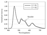
도 4는 본 발명의 실시예 1과 실시예 2에 따른 유기 발광 소자의 파장대별 발광세기를 보여주는 그래프이다. 도 4에서 실시예 1은 전술한 도 2에 따른 유기 발광 소자이고, 실시예는 전술한 도 3에 따른 유기 발광 소자이다. 4 is a graph showing the intensity of light emitted by the organic light emitting device according to Example 1 and Example 2 of the present invention. In FIG. 4, Example 1 is the organic light emitting device according to the above-described FIG. 2, and the embodiment is the organic light emitting device according to FIG.
도 4에서 알 수 있듯이, 적색(R)을 발광하는 제2 발광층(2nd EML)과 녹색(G)을 발광하는 제3 발광층(3rd EML) 사이에 발광 조절층(ECL)을 구비한 실시예 2가 상기 발광 조절층(ECL)을 구비하지 않은 실시예 1에 비하여 대략 520nm의 녹색(G) 파장대의 발광세기가 향상됨을 알 수 있다. 4, a second emission layer (2nd EML) emitting red (R) and a third emission layer (3rd EML) emitting green (G) The emission intensity of the green (G) wavelength band of about 520 nm is improved as compared with Example 1 in which the emission control layer (ECL) is not provided.
또한, 실시예 2가 실시예 1에 비하여 장파장대의 쇼율더(shoulder) 부분이 줄어들게 되어 색순도가 향상됨을 알 수 있다. In addition, it can be seen that the color purity is improved by reducing the shoulder portion of the long wavelength band in Example 2 compared to Example 1. [
도 5는 본 발명의 실시예 1과 실시예 2에 따른 유기 발광 소자의 시야각에 따른 색변화율을 보여주는 그래프이다. 도 5에서 실시예 1은 전술한 도 2에 따른 유기 발광 소자이고, 실시예는 전술한 도 3에 따른 유기 발광 소자이다. 5 is a graph showing a color change ratio according to viewing angles of organic light emitting devices according to Example 1 and Example 2 of the present invention. In FIG. 5, Example 1 is the organic light emitting device according to the above-described FIG. 2, and the embodiment is the organic light emitting device according to FIG.
도 5에서 알 수 있듯이, 적색(R)을 발광하는 제2 발광층(2nd EML)과 녹색(G)을 발광하는 제3 발광층(3rd EML) 사이에 발광 조절층(ECL)을 구비한 실시예 2가 상기 발광 조절층(ECL)을 구비하지 않은 실시예 1에 비하여 시야각에 따른 색변화율이 줄어드는 것을 알 수 있다. 따라서, 상기 발광 조절층(ECL)을 구비한 실시예 2가 상기 발광 조절층(ECL)을 구비하지 않은 실시예 1에 비하여 색시야각 특성이 향상됨을 알 수 있다. As shown in FIG. 5, in Example 2 (EML) having a light emission control layer (ECL) between a second emission layer (2nd emission layer) emitting red (R) and a third emission layer The color change ratio according to the viewing angle decreases compared to Example 1 in which the emission control layer (ECL) is not provided. Therefore, it can be seen that the color viewing angle characteristic of Example 2 having the emission control layer (ECL) is improved as compared with Example 1 having no emission control layer (ECL).
전술한 바와 같이, 상기 발광 조절층(ECL)은 전자 수송 특성을 구비한 재료와 정공 수송 특성을 구비한 재료의 혼합물, 또는 양극성(bipolar) 재료로 이루어질 수 있다. 상기 발광 조절층(ECL)이 전자 수송 특성을 구비한 재료와 정공 수송 특성을 구비한 혼합물로 이루어진 경우, 상기 전자 수송 특성을 구비한 재료와 상기 정공 수송 특성을 구비한 재료 사이의 혼합비율은 3:7~7:3의 범위가 바람직하다. As described above, the emission control layer (ECL) may be a mixture of a material having an electron transporting property and a material having a hole transporting property, or a bipolar material. When the emission control layer (ECL) is made of a material having an electron transporting property and a mixture having a hole transporting property, the mixing ratio between the material having the electron transporting property and the material having the hole transporting property is 3 : 7 to 7: 3.
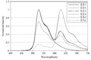
도 6은 다양한 조성을 가지는 발광 조절층을 적용함에 따른 파장대별 발광세기 변화를 보여주는 그래프로서, 이는 아래 표 1의 샘플 1 내지 샘플 6에 따른 조성의 발광 조절층을 적용한 것이다. FIG. 6 is a graph showing changes in luminescence intensities according to wavelengths as the emission control layer having various compositions is applied, which is a result of applying the emission control layer having the composition according to
아래 표 1은 제1 샘플 내지 제6 샘플 각각에 대한 외부양자효율(external quantum efficiency; EQE), 및 녹색(Green)과 적색(Red)의 정규화된 발광세기(Normalized Intensity) 결과를 보여준다. Table 1 below shows the external quantum efficiency (EQE) for each of the first to sixth samples and the normalized intensity results of green and red.
EQE
위의 표 1에서, 샘플 1은 정공 수송 특성을 구비한 재료(P-type)만으로 이루어진 발광 조절층(ECL)을 이용한 것이고, 샘플 2는 정공 수송 특성을 구비한 재료(P-type)와 전자 수송 특성을 구비한 재료(E-type)의 중량비가 7:3으로 이루어진 발광 조절층(ECL)을 이용한 것이고, 샘플 3은 정공 수송 특성을 구비한 재료(P-type)와 전자 수송 특성을 구비한 재료(E-type)의 중량비가 5:5으로 이루어진 발광 조절층(ECL)을 이용한 것이고, 샘플 4는 정공 수송 특성을 구비한 재료(P-type)와 전자 수송 특성을 구비한 재료(E-type)의 중량비가 3:7로 이루어진 발광 조절층(ECL)을 이용한 것이고, 샘플 5는 전자 수송 특성을 구비한 재료(E-type)만으로 이루어진 발광 조절층(ECL)을 이용한 것이고, 샘플 6은 양극성(bipolar) 재료로 이루어진 발광 조절층(ECL)을 이용한 것이다. In Table 1,
도 6 및 표 1을 참조하면, 샘플 2, 샘플 3, 샘플 4, 및 샘플 6은 외부양자효율(external quantum efficiency; EQE)이 우수하고 녹색(Green) 및 적색(Red)의 정규화된 발광세기(Normalized Intensity)도 우수함을 알 수 있다. Referring to FIG. 6 and Table 1, Sample 2, Sample 3, Sample 4, and Sample 6 have excellent external quantum efficiency (EQE) and normalized luminescence intensity of green and red Normalized Intensity) is also excellent.
따라서, 상기 발광 조절층(ECL)은 양극성(bipolar) 재료로 이루어지거나 또는 전자 수송 특성을 구비한 재료와 정공 수송 특성을 구비한 재료 사이의 혼합비율이 3:7~7:3의 범위를 가지는 것이 바람직함을 알 수 있다. Therefore, the emission control layer (ECL) may be formed of a bipolar material, or a mixture of materials having electron transport properties and materials having hole transport properties in a range of 3: 7 to 7: 3 Is preferable.
특히, 샘플 2, 샘플 3, 및 샘플 4 중에서 샘플 3의 경우가 샘플 2 및 샘플 4에 비하여 외부양자효율(external quantum efficiency; EQE)과 녹색(Green) 및 적색(Red)의 정규화된 발광세기(Normalized Intensity)가 우수함을 알 수 있다. Particularly, in Sample 2, Sample 3, and Sample 4, the case of Sample 3 has an external quantum efficiency (EQE) and a normalized luminescence intensity of Green (Green) and Red (Red) Normalized Intensity) is superior.
따라서, 상기 발광 조절층(ECL)이 전자 수송 특성을 구비한 재료와 정공 수송 특성을 구비한 재료의 혼합물로 이루어진 경우, 전자 수송 특성을 구비한 재료와 정공 수송 특성을 구비한 재료 사이의 혼합비율은 5:5인 것이 더욱 바람직함을 알 수 있다. Therefore, when the emission control layer (ECL) is made of a mixture of a material having an electron transporting property and a material having a hole transporting property, a mixing ratio between a material having an electron transporting property and a material having a hole transporting property Is more preferably 5: 5.
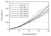
도 7은 발광 조절층(ECL)의 두께 변화에 따른 색시야각 특성 변화를 보여주는 그래프이다.7 is a graph showing changes in color viewing angle characteristics according to the thickness of the emission control layer (ECL).
도 7은 도 3에 따른 유기 발광 소자에서 발광 조절층(ECL)의 두께가 변화함에 따라 색시야각 특성이 변화하는 모습을 보여준다. 도 7에서 알 수 있듯이, 발광 조절층(ECL)의 두께가 50Å, 100Å, 및 200Å으로 증가함에 따라 60°의 시야각에서 색변화율은 점차로 감소하다고, 발광 조절층(ECL)의 두께가 250Å 및 300Å으로 증가하게 되면 60°의 시야각에서 색변화율은 다시 점차로 증가함을 알 수 있다. FIG. 7 shows the color viewing angle characteristics of the organic light emitting device according to FIG. 3 as the thickness of the emission control layer (ECL) changes. As can be seen from FIG. 7, as the thickness of the emission control layer (ECL) increases to 50 A, 100 A and 200 A, the color change rate gradually decreases at a viewing angle of 60 deg., While the thickness of the emission control layer (ECL) It can be seen that the color change rate gradually increases at a viewing angle of 60 °.
특히, 발광 조절층(ECL)의 두께가 300Å인 경우는 발광 조절층(ECL)이 적용되지 않은 경우(ECL 0)에 비하여 60°의 시야각에서 색변화율이 오히려 크게 됨을 알 수 있다. Particularly, when the thickness of the emission control layer (ECL) is 300 ANGSTROM, the color change ratio is rather large at a viewing angle of 60 DEG in comparison with the case where the emission control layer (ECL) is not applied (ECL 0).
따라서, 상기 발광 조절층(ECL)의 두께는 300Å미만으로 설정하는 것이 바람직하다. Therefore, the thickness of the emission control layer (ECL) is preferably set to less than 300 ANGSTROM.
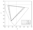
도 8은 비교예, 실시예 1, 및 실시예 2에 따른 유기 발광 소자의 파장대별 발광 세기를 보여주는 그래프이고, 도 9는 비교예, 실시예 1, 및 실시예 2에 따른 유기 발광 소자의 색 영역을 보여주는 그래프이고, 도 10은 비교예, 실시예 1, 및 실시예 2에 따른 유기 발광 소자의 시야각에 따른 색변화율을 보여주는 그래프이다. FIG. 8 is a graph showing the luminescence intensities of the organic luminescent devices according to Comparative Examples, Examples 1 and 2, and FIG. 9 is a graph showing the luminescence intensity of the organic luminescent devices according to Comparative Examples, Examples 1 and 2 And FIG. 10 is a graph showing a color change ratio according to viewing angles of the organic light emitting diode according to the comparative example, the first embodiment, and the second embodiment.
아래 표 2는 비교예, 실시예 1 및 실시예 2에 따른 유기 발광 소자에 대한 도 8 내지 도 10의 결과를 보여준다. Table 2 below shows the results of Figs. 8 to 10 for the organic luminescent device according to Comparative Example, Example 1 and Example 2. Fig.
The second stack
(%)G efficiency
(%)
(%)R efficiency
(%)
중첩비(
BT2020
Overlap ratio
(△u'v')Viewing angle
(? U'v ')
표 2에서, 비교예는 전술한 도 2에 따른 유기 발광 소자에서 제3 발광층(3rd EML)으로 녹색(G) 대신에 황녹색(YG)을 발광하는 발광층을 이용한 것이고, 실시예 1은 전술한 도 2에 따른 유기 발광 소자이고, 실시예 2는 전술한 도 3에 따른 유기 발광 소자이다. In Table 2, the comparative example uses a light emitting layer that emits yellow green (YG) instead of green (G) as the third emitting layer (3rd EML) in the organic light emitting device according to the aforementioned FIG. 2, FIG. 2 is an organic light emitting device, and FIG. 2 is an organic light emitting device according to the previously described FIG.
도 8 및 표 2에서 알 수 있듯이, 실시예 1 및 실시예 2의 경우가 비교예에 비하여 적색(R) 광의 발광 효율은 떨어지지만 녹색(G) 광의 발광 효율이 향상됨을 알 수 있다. 즉, 도 8에서 알 수 있듯이, 녹색 컬러층(Green CL)의 피크 파장은 실시예 1 및 실시예 2의 녹색 파장대의 피크 파장과 일치함을 알 수 있다. As can be seen from FIG. 8 and Table 2, the luminous efficiency of the red (R) light is lower than that of the comparative example in Examples 1 and 2, but the luminous efficiency of the green (G) light is improved. That is, as can be seen from FIG. 8, the peak wavelength of the green color layer (Green CL) agrees with the peak wavelength of the green wavelength band of the first and second embodiments.
따라서, 실시예 1 및 실시예 2의 경우가 비교예에 비하여 색순도가 향상될 수 있다. 특히, 실시예 2의 경우가 실시예 1에 비하여 녹색(G) 광의 발광 효율이 향상되어 색순도가 우수함을 알 수 있다. Therefore, the color purity in Examples 1 and 2 can be improved as compared with Comparative Examples. Particularly, in the case of Example 2, the luminous efficiency of green (G) light is improved and the color purity is excellent as compared with Example 1.
도 9 및 표 2에서 알 수 있듯이, 실시예 1 및 실시예 2의 경우가 비교예에 비하여 표현할 수 있는 색상 범위가 넓고 따라서 색재현율이 향상됨을 알 수 있다. 특히, 실시예 2의 경우가 실시예 1에 비하여 표현할 수 있는 색상 범위가 넓고 따라서 색재현율이 향상된다.As can be seen from FIG. 9 and Table 2, it can be seen that the color gamut of Example 1 and Example 2 is broader than that of Comparative Example, and thus the color gamut is improved. Particularly, in the case of the embodiment 2, the color range that can be expressed is wider than in the
도 10 및 표 2에서 알 수 있듯이, 실시예 1 및 실시예 2는 비교예에 비하여 60°의 시야각에서 색변화율이 다소 큼을 알 수 있다. 그러나, 실시예 2는 실시예 1에 비하여 60°의 시야각에서 색변화율이 작고 비교예와의 차이가 크지 않음을 알 수 있다. 따라서, 실시예 2의 경우 실시예 1에 비하여 색시야각 특성이 향상됨을 알 수 있다. 10 and Table 2, it can be seen that the color change ratio is slightly larger in Example 1 and Example 2 at a viewing angle of 60 ° than the comparative example. However, in Example 2, the color change ratio is small at a viewing angle of 60 DEG in comparison with Example 1, and the difference from Comparative Example is not large. Therefore, it can be seen that the color viewing angle characteristics of Example 2 are improved compared to Example 1. [
도 11은 본 발명의 일 실시예에 따른 유기 발광 표시 장치의 개략적인 단면도로서, 이는 전술한 도 2 또는 도 3에 따른 유기 발광 소자를 적용한 것이다. FIG. 11 is a schematic cross-sectional view of an organic light emitting diode display according to an embodiment of the present invention, which is applied to the organic light emitting diode according to FIG. 2 or FIG.
도 11에서 알 수 있듯이, 본 발명의 일 실시예에 따른 유기 발광 표시 장치는 기판(10), 박막 트랜지스터층(20), 평탄화층(30), 제1 전극(40), 뱅크층(50), 유기층(60), 및 제2 전극(70)을 포함하여 이루어진다. 11, the organic light emitting diode display according to an exemplary embodiment of the present invention includes a
상기 기판(10)은 유리 또는 구부리거나 휠 수 있는 투명한 플라스틱, 예로서, 폴리이미드가 이용될 수 있지만, 반드시 그에 한정되는 것은 아니다. The
상기 박막 트랜지스터층(20)은 상기 기판(10) 상에서 형성되어 있다. 이와 같은 박막 트랜지스터층(20)은 게이트 전극(21), 게이트 절연막(22), 반도체층(23), 소스 전극(24a), 드레인 전극(24b), 및 보호막(25)을 포함하여 이루어진다. The thin
상기 게이트 전극(21)은 상기 기판(10) 상에 패턴 형성되어 있고, 상기 게이트 절연막(22)은 상기 게이트 전극(21) 상에 형성되어 있고, 상기 반도체층(23)은 상기 게이트 절연막(22) 상에 패턴 형성되어 있고, 상기 소스 전극(24a)과 상기 드레인 전극(24b)은 상기 반도체층(23) 상에서 서로 마주하도록 패턴 형성되어 있고, 상기 보호막(25)은 상기 소스 전극(24a)과 상기 드레인 전극(24b) 상에 형성되어 있다.The
도면에는 게이트 전극(21)이 반도체층(23) 아래에 형성되는 바텀 게이트(bottom gate) 구조를 도시하였지만, 게이트 전극(21)이 반도체층(23) 위에 형성되는 탑 게이트(top gate) 구조로 이루어질 수도 있다. Although the bottom gate structure in which the
상기 평탄화층(30)은 상기 박막 트랜지스터층(20) 상에 형성되어 기판 표면을 평탄화시킨다. 이와 같은 평탄화층(30)은 포토 아크릴과 같은 유기 절연막으로 이루어질 수 있지만, 반드시 그에 한정되는 것은 아니다. The
상기 제1 전극(40)은 상기 평탄화층(30) 상에 형성되어 있다. 상기 제1 전극(40)은 상기 보호막(25) 및 상기 평탄화층(30)에 구비된 콘택홀을 통해서 상기 박막 트랜지스터층(20)의 드레인 전극(24b) 또는 소스 전극(24a)과 연결되어 있다. The first electrode (40) is formed on the planarization layer (30). The
상기 제1 전극(40)은 전술한 다양한 실시예의 양극(Anode)으로 이루어질 수 있다. The
상기 뱅크층(50)은 상기 제1 전극(40) 및 상기 평탄화층(30) 상에 형성되어 화소 영역을 정의한다. 상기 뱅크층(50)은 복수의 화소들 사이의 경계 영역에 매트릭스 구조로 형성됨으로써, 상기 뱅크층(50)에 의해서 화소 영역이 정의된다.The
상기 유기층(60)은 상기 제1 전극(40) 상에 형성되어 있다. 상기 유기층(60)은 상기 뱅크층(50) 상에도 형성될 수 있다. 즉, 상기 유기층(60)은 화소 별로 분리되지 않고 인접하는 화소 사이에 서로 연결될 수 있다. The
상기 유기층(60)은 전술한 도 2 또는 도 3의 제1 스택(1st Stack), 제1 전하 생성층(1st CGL), 제2 스택(2nd Stack), 제2 전하 생성층(2nd CGL), 및 제3 스택(3rd Stack)의 적층 구조로 이루어질 수도 있다. 따라서, 상기 유기층(60)에서는 백색(White) 광이 방출될 수 있다. The
상기 제2 전극(70)은 상기 유기층(60) 상에 형성되어 있다. 상기 제2 전극(70)은 전술한 다양한 실시예의 음극(Cathode)으로 이루어질 수 있다. The second electrode (70) is formed on the organic layer (60). The
이와 같은 상기 제1 전극(30), 유기층(60), 및 제2 전극(70)의 적층 구조는 전술한 도 2 또는 도 3에 따른 유기 발광 소자로 이루어질 수 있다. The stacked structure of the
한편, 도시하지는 않았지만, 개별 화소에는 상기 유기층(60)에서 방출되는 백색(White) 광을 파장 별로 필터링하기 위한 컬러 필터가 추가로 구비될 수 있다. 상기 컬러 필터는 광의 이동경로 상에 형성된다. 즉, 상기 유기층(60)에서 방출된 광이 하부의 기판(10) 방향으로 진행하는 소위 바텀 에미션(Bottom Emission) 방식의 경우에는 상기 컬러 필터가 상기 유기층(60)의 아래에 형성되고, 상기 유기층(60)에서 방출된 광이 상부의 제2 전극(70) 방향으로 진행하는 소위 탑 에미션(Top Emission) 방식의 경우에는 상기 컬러 필터가 상기 유기층(60)의 위에 형성된다. Although not shown, individual pixels may further include a color filter for filtering the white light emitted from the
또한, 이상은 상기 양극(Anode)이 투명전극으로 이루어지고 상기 음극(Cathode)이 반사전극으로 이루어져 상기 제1 스택(1st Stack), 제2 스택(2nd Stack) 및 제3 스택(3rd Stack)에서 발광한 광이 상기 양극(Anode) 방향으로 방출되는 하부 발광 유기 발광소자에 대해서 설명하였지만, 본 발명이 반드시 그에 한정되는 것은 아니고, 상기 양극(Anode)이 반사전극으로 이루어지고 상기 음극(Cathode)이 투명전극으로 이루어져 상기 제1 스택(1st Stack), 제2 스택(2nd Stack) 및 제3 스택(3rd Stack)에서 발광한 광이 상기 음극(Cathode) 방향으로 방출되는 상부 발광 유기 발광소자도 포함한다. In the above description, the anode is a transparent electrode and the cathode is a reflective electrode. The first stack, the second stack, and the third stack The present invention is not necessarily limited to this. The anode may be a reflective electrode, and the cathode may be a cathode. In this case, And an upper light emitting organic light emitting device formed of a transparent electrode and emitting light emitted in the first stack, the second stack, and the third stack (third stack) in the direction of the cathode (cathode) .
상기 상부 발광 유기 발광 소자의 경우 상기 제2 스택(2nd Stack) 내에 구비된 적색(R)을 발광하는 제2 발광층(2nd EML)이 녹색(G)을 발광하는 제3 발광층(3rd EML)보다 상기 투명전극인 음극(Cathode)에 보다 가깝게 배치될 수 있다. In the case of the upper light emitting organic light emitting device, the second emission layer (2nd EML) emitting red (R), provided in the second stack (2nd Stack) And can be disposed closer to the cathode, which is a transparent electrode.
이상 첨부된 도면을 참조하여 본 발명의 실시예들을 더욱 상세하게 설명하였으나, 본 발명은 반드시 이러한 실시예로 국한되는 것은 아니고, 본 발명의 기술사상을 벗어나지 않는 범위 내에서 다양하게 변형 실시될 수 있다. 따라서, 본 발명에 개시된 실시예들은 본 발명의 기술 사상을 한정하기 위한 것이 아니라 설명하기 위한 것이고, 이러한 실시예에 의하여 본 발명의 기술 사상의 범위가 한정되는 것은 아니다. 그러므로, 이상에서 기술한 실시예들은 모든 면에서 예시적인 것이며 한정적이 아닌 것으로 이해해야만 한다. 본 발명의 보호 범위는 청구 범위에 의하여 해석되어야 하며, 그와 동등한 범위 내에 있는 모든 기술 사상은 본 발명의 권리 범위에 포함되는 것으로 해석되어야 할 것이다 Although the embodiments of the present invention have been described in detail with reference to the accompanying drawings, it is to be understood that the present invention is not limited to those embodiments and various changes and modifications may be made without departing from the scope of the present invention. . Therefore, the embodiments disclosed in the present invention are intended to illustrate rather than limit the scope of the present invention, and the scope of the technical idea of the present invention is not limited by these embodiments. Therefore, it should be understood that the above-described embodiments are illustrative in all aspects and not restrictive. The scope of protection of the present invention should be construed according to the claims, and all technical ideas within the scope of the same should be interpreted as being included in the scope of the present invention
10: 기판 20: 박막 트랜지스터층
30: 평탄화층 40: 제1 전극
50: 뱅크층 60: 유기층
70: 제2 전극10: substrate 20: thin film transistor layer
30: planarization layer 40: first electrode
50: bank layer 60: organic layer
70: Second electrode
Claims (11)
상기 양극과 상기 음극 사이에 구비된 제1 스택, 제2 스택, 및 제3 스택;
상기 제1 스택과 상기 제2 스택 사이에 구비된 제1 전하 생성층 및 상기 제2 스택과 상기 제3 스택 사이에 구비된 제2 전하 생성층을 포함하여 이루어지고,
상기 제2 스택은 서로 상이한 층에 적층된 적색 발광층 및 녹색 발광층을 포함하여 이루어진 유기 발광 소자. Anode and cathode;
A first stack, a second stack, and a third stack provided between the anode and the cathode;
A first charge generation layer provided between the first stack and the second stack, and a second charge generation layer provided between the second stack and the third stack,
Wherein the second stack includes a red light emitting layer and a green light emitting layer stacked in layers different from each other.
상기 적색 발광층과 상기 녹색 발광층은 서로 이격되어 있는 유기 발광 소자. The method according to claim 1,
Wherein the red light emitting layer and the green light emitting layer are spaced apart from each other.
상기 적색 발광층과 상기 녹색 발광층 사이에 발광 조절층이 추가로 구비되고, 상기 발광 조절층에 의해서 상기 적색 발광층과 상기 녹색 발광층이 서로 이격되어 있는 유기 발광 소자. 3. The method of claim 2,
Wherein an emission control layer is additionally provided between the red emission layer and the green emission layer, and the red emission layer and the green emission layer are separated from each other by the emission control layer.
상기 발광 조절층은 전자 수송 특성을 구비한 재료와 정공 수송 특성을 구비한 재료의 혼합물로 이루어진 유기 발광 소자. The method of claim 3,
Wherein the emission control layer comprises a mixture of a material having an electron transporting property and a material having a hole transporting property.
상기 전자 수송 특성을 구비한 재료와 정공 수송 특성을 구비한 재료 사이의 혼합비율은 3:7 ~ 7:3의 범위인 유기 발광 소자. 5. The method of claim 4,
Wherein the mixing ratio between the material having the electron transporting property and the material having the hole transporting property is in the range of 3: 7 to 7: 3.
상기 발광 조절층은 전자 수송 특성과 정공 수송 특성을 구비한 양극성 재료로 이루어진 유기 발광 소자. The method of claim 3,
Wherein the emission control layer is made of a bipolar material having an electron transporting property and a hole transporting property.
상기 발광 조절층의 두께는 300Å미만으로 이루어진 유기 발광 소자. The method of claim 3,
Wherein the thickness of the emission control layer is less than 300 ANGSTROM.
상기 양극과 음극 중에서 어느 하나는 반사 전극으로 이루어지고 나머지 하나는 투명 전극으로 이루어지고,
상기 적색 발광층은 상기 투명 전극에 가깝게 배치되고, 상기 녹색 발광층은 상기 반사 전극에 가깝게 배치되는 유기 발광 소자. The method according to claim 1,
Wherein one of the anode and the cathode is a reflective electrode and the other is a transparent electrode,
Wherein the red light emitting layer is disposed close to the transparent electrode, and the green light emitting layer is disposed close to the reflective electrode.
상기 제1 스택은 상기 양극에 가장 가깝게 배치되고, 상기 제3 스택은 상기 음극에 가장 가깝게 배치되고, 상기 제1 스택과 상기 제3 스택은 각각 청색 발광층을 포함하여 이루어진 유기 발광 소자. The method according to claim 1,
Wherein the first stack is disposed closest to the anode and the third stack is disposed closest to the cathode, wherein the first stack and the third stack each include a blue light emitting layer.
상기 제2 스택과 상기 제3 스택은 각각 정공 수송층을 포함하여 이루어지고,
상기 제3 스택의 정공 수송층의 두께는 상기 제2 스택의 정공 수송층의 두께보다 두꺼운 유기 발광 소자. The method according to claim 1,
Wherein the second stack and the third stack each comprise a hole transport layer,
Wherein the thickness of the hole transport layer of the third stack is thicker than the thickness of the hole transport layer of the second stack.
상기 기판 상에 구비된 박막 트랜지스터층; 및
상기 박막 트랜지스터층 상에 구비된 유기 발광 소자를 포함하여 이루어지고,
상기 유기 발광 소자는 전술한 제1항 내지 제10항 중 어느 한 항에 따른 유기 발광 소자로 이루어진 유기 발광 표시 장치. Board;
A thin film transistor layer provided on the substrate; And
And an organic light emitting element provided on the thin film transistor layer,
Wherein the organic light emitting device comprises the organic light emitting device according to any one of claims 1 to 10.
Priority Applications (1)
| Application Number | Priority Date | Filing Date | Title |
|---|---|---|---|
| KR1020160162259A KR102721716B1 (en) | 2016-11-30 | 2016-11-30 | Organic Light Emitting Device and Organic Light Emitting Display Apparatus using the same |
Applications Claiming Priority (1)
| Application Number | Priority Date | Filing Date | Title |
|---|---|---|---|
| KR1020160162259A KR102721716B1 (en) | 2016-11-30 | 2016-11-30 | Organic Light Emitting Device and Organic Light Emitting Display Apparatus using the same |
Publications (2)
| Publication Number | Publication Date |
|---|---|
| KR20180062222A true KR20180062222A (en) | 2018-06-08 |
| KR102721716B1 KR102721716B1 (en) | 2024-10-23 |
Family
ID=62600625
Family Applications (1)
| Application Number | Title | Priority Date | Filing Date |
|---|---|---|---|
| KR1020160162259A Active KR102721716B1 (en) | 2016-11-30 | 2016-11-30 | Organic Light Emitting Device and Organic Light Emitting Display Apparatus using the same |
Country Status (1)
| Country | Link |
|---|---|
| KR (1) | KR102721716B1 (en) |
Cited By (1)
| Publication number | Priority date | Publication date | Assignee | Title |
|---|---|---|---|---|
| KR20200135744A (en) * | 2019-05-23 | 2020-12-03 | 유니버셜 디스플레이 코포레이션 | Oled display panel with unpatterned emissive stack |
Citations (4)
| Publication number | Priority date | Publication date | Assignee | Title |
|---|---|---|---|---|
| KR20140079273A (en) * | 2012-12-18 | 2014-06-26 | 엘지디스플레이 주식회사 | White organic light emitting device |
| KR20160065268A (en) * | 2014-11-28 | 2016-06-09 | 엘지디스플레이 주식회사 | Organic light emitting display device |
| KR20160067668A (en) * | 2014-12-04 | 2016-06-14 | 엘지디스플레이 주식회사 | Organic light emitting device and display device having thereof |
| KR20160068996A (en) * | 2014-12-05 | 2016-06-16 | 엘지디스플레이 주식회사 | Organic Light Emitting Device and Organic Light Emitting Display Device using the same |
-
2016
- 2016-11-30 KR KR1020160162259A patent/KR102721716B1/en active Active
Patent Citations (4)
| Publication number | Priority date | Publication date | Assignee | Title |
|---|---|---|---|---|
| KR20140079273A (en) * | 2012-12-18 | 2014-06-26 | 엘지디스플레이 주식회사 | White organic light emitting device |
| KR20160065268A (en) * | 2014-11-28 | 2016-06-09 | 엘지디스플레이 주식회사 | Organic light emitting display device |
| KR20160067668A (en) * | 2014-12-04 | 2016-06-14 | 엘지디스플레이 주식회사 | Organic light emitting device and display device having thereof |
| KR20160068996A (en) * | 2014-12-05 | 2016-06-16 | 엘지디스플레이 주식회사 | Organic Light Emitting Device and Organic Light Emitting Display Device using the same |
Cited By (1)
| Publication number | Priority date | Publication date | Assignee | Title |
|---|---|---|---|---|
| KR20200135744A (en) * | 2019-05-23 | 2020-12-03 | 유니버셜 디스플레이 코포레이션 | Oled display panel with unpatterned emissive stack |
Also Published As
| Publication number | Publication date |
|---|---|
| KR102721716B1 (en) | 2024-10-23 |
Similar Documents
| Publication | Publication Date | Title |
|---|---|---|
| KR101666781B1 (en) | Organic Light Emitting Device | |
| KR102125881B1 (en) | Organic light emitting device | |
| KR102311911B1 (en) | Organic Light Emitting Device and Organic Light Emitting Display Device using the same | |
| KR102142620B1 (en) | Organic light emitting display device | |
| KR20180078641A (en) | Organic Light Emitting Device and Organic Light Emitting Display Apparatus using the same | |
| KR102863119B1 (en) | Organic Light Emitting Device and Organic Light Emitting Display Apparatus using the same | |
| KR102353804B1 (en) | Organic light emitting device | |
| KR20150113308A (en) | Organic Light Emitting Device | |
| KR102831231B1 (en) | Organic Light Emitting Device and Organic Light Emitting Display Apparatus using the same | |
| KR101941084B1 (en) | Organic Light Emitting Diode Device | |
| KR102920681B1 (en) | Organic light emitting display apparatus | |
| KR102339125B1 (en) | Organic light emitting device | |
| KR102081248B1 (en) | Organic light emitting diode display | |
| KR20250058730A (en) | Organic light emitting device | |
| KR102283502B1 (en) | Organic Light Emitting Device and Organic Light Emitting Display Device using the same | |
| KR102762804B1 (en) | Organic light emitting diode and organic light emitting diode display comprising the same | |
| KR20180078637A (en) | Organic Light Emitting Device and Organic Light Emitting Display Apparatus using the same | |
| KR20160082895A (en) | Organic Light Emitting Device and Method of manufacturing the same and Organic Light Emitting Display Device using the same | |
| KR20160073461A (en) | Organic light emitting display device | |
| KR20180062234A (en) | Organic Light Emitting Device and Organic Light Emitting Display Apparatus using the same | |
| KR102721716B1 (en) | Organic Light Emitting Device and Organic Light Emitting Display Apparatus using the same | |
| KR102760908B1 (en) | Organic light emitting device and organic light emitting display device comprising the same | |
| KR102722601B1 (en) | Organic Light Emitting Device and Organic Light Emitting Display Apparatus using the same | |
| KR102440454B1 (en) | Electroluminescence display device | |
| KR102275954B1 (en) | Organic Light Emitting Device and Organic Light Emitting Display Device using the same |
Legal Events
| Date | Code | Title | Description |
|---|---|---|---|
| PA0109 | Patent application |
St.27 status event code: A-0-1-A10-A12-nap-PA0109 |
|
| PG1501 | Laying open of application |
St.27 status event code: A-1-1-Q10-Q12-nap-PG1501 |
|
| A201 | Request for examination | ||
| PA0201 | Request for examination |
St.27 status event code: A-1-2-D10-D11-exm-PA0201 |
|
| P22-X000 | Classification modified |
St.27 status event code: A-2-2-P10-P22-nap-X000 |
|
| P22-X000 | Classification modified |
St.27 status event code: A-2-2-P10-P22-nap-X000 |
|
| D13-X000 | Search requested |
St.27 status event code: A-1-2-D10-D13-srh-X000 |
|
| D14-X000 | Search report completed |
St.27 status event code: A-1-2-D10-D14-srh-X000 |
|
| E902 | Notification of reason for refusal | ||
| PE0902 | Notice of grounds for rejection |
St.27 status event code: A-1-2-D10-D21-exm-PE0902 |
|
| E13-X000 | Pre-grant limitation requested |
St.27 status event code: A-2-3-E10-E13-lim-X000 |
|
| P11-X000 | Amendment of application requested |
St.27 status event code: A-2-2-P10-P11-nap-X000 |
|
| P13-X000 | Application amended |
St.27 status event code: A-2-2-P10-P13-nap-X000 |
|
| E601 | Decision to refuse application | ||
| PE0601 | Decision on rejection of patent |
St.27 status event code: N-2-6-B10-B15-exm-PE0601 |
|
| T11-X000 | Administrative time limit extension requested |
St.27 status event code: U-3-3-T10-T11-oth-X000 |
|
| T13-X000 | Administrative time limit extension granted |
St.27 status event code: U-3-3-T10-T13-oth-X000 |
|
| AMND | Amendment | ||
| E13-X000 | Pre-grant limitation requested |
St.27 status event code: A-2-3-E10-E13-lim-X000 |
|
| P11-X000 | Amendment of application requested |
St.27 status event code: A-2-2-P10-P11-nap-X000 |
|
| P13-X000 | Application amended |
St.27 status event code: A-2-2-P10-P13-nap-X000 |
|
| PX0901 | Re-examination |
St.27 status event code: A-2-3-E10-E12-rex-PX0901 |
|
| PX0701 | Decision of registration after re-examination |
St.27 status event code: A-3-4-F10-F13-rex-PX0701 |
|
| GRNT | Written decision to grant | ||
| PR0701 | Registration of establishment |
St.27 status event code: A-2-4-F10-F11-exm-PR0701 |
|
| PR1002 | Payment of registration fee |
St.27 status event code: A-2-2-U10-U11-oth-PR1002 Fee payment year number: 1 |
|
| PG1601 | Publication of registration |
St.27 status event code: A-4-4-Q10-Q13-nap-PG1601 |