KR20180040792A - Method of arranging conductive pattern, conductive pattern structure formed by using the same, conductive mesh, photomask, stamper, touch screen panel - Google Patents
Method of arranging conductive pattern, conductive pattern structure formed by using the same, conductive mesh, photomask, stamper, touch screen panel Download PDFInfo
- Publication number
- KR20180040792A KR20180040792A KR1020160132501A KR20160132501A KR20180040792A KR 20180040792 A KR20180040792 A KR 20180040792A KR 1020160132501 A KR1020160132501 A KR 1020160132501A KR 20160132501 A KR20160132501 A KR 20160132501A KR 20180040792 A KR20180040792 A KR 20180040792A
- Authority
- KR
- South Korea
- Prior art keywords
- conductive
- conductive lines
- standard deviation
- set pitch
- average
- Prior art date
- Legal status (The legal status is an assumption and is not a legal conclusion. Google has not performed a legal analysis and makes no representation as to the accuracy of the status listed.)
- Ceased
Links
Images


Classifications
-
- G—PHYSICS
- G06—COMPUTING OR CALCULATING; COUNTING
- G06F—ELECTRIC DIGITAL DATA PROCESSING
- G06F3/00—Input arrangements for transferring data to be processed into a form capable of being handled by the computer; Output arrangements for transferring data from processing unit to output unit, e.g. interface arrangements
- G06F3/01—Input arrangements or combined input and output arrangements for interaction between user and computer
- G06F3/03—Arrangements for converting the position or the displacement of a member into a coded form
- G06F3/041—Digitisers, e.g. for touch screens or touch pads, characterised by the transducing means
- G06F3/044—Digitisers, e.g. for touch screens or touch pads, characterised by the transducing means by capacitive means
- G06F3/0445—Digitisers, e.g. for touch screens or touch pads, characterised by the transducing means by capacitive means using two or more layers of sensing electrodes, e.g. using two layers of electrodes separated by a dielectric layer
-
- H—ELECTRICITY
- H01—ELECTRIC ELEMENTS
- H01B—CABLES; CONDUCTORS; INSULATORS; SELECTION OF MATERIALS FOR THEIR CONDUCTIVE, INSULATING OR DIELECTRIC PROPERTIES
- H01B13/00—Apparatus or processes specially adapted for manufacturing conductors or cables
- H01B13/0036—Details
-
- G—PHYSICS
- G06—COMPUTING OR CALCULATING; COUNTING
- G06F—ELECTRIC DIGITAL DATA PROCESSING
- G06F3/00—Input arrangements for transferring data to be processed into a form capable of being handled by the computer; Output arrangements for transferring data from processing unit to output unit, e.g. interface arrangements
- G06F3/01—Input arrangements or combined input and output arrangements for interaction between user and computer
- G06F3/03—Arrangements for converting the position or the displacement of a member into a coded form
- G06F3/041—Digitisers, e.g. for touch screens or touch pads, characterised by the transducing means
- G06F3/044—Digitisers, e.g. for touch screens or touch pads, characterised by the transducing means by capacitive means
- G06F3/0448—Details of the electrode shape, e.g. for enhancing the detection of touches, for generating specific electric field shapes, for enhancing display quality
-
- H—ELECTRICITY
- H01—ELECTRIC ELEMENTS
- H01B—CABLES; CONDUCTORS; INSULATORS; SELECTION OF MATERIALS FOR THEIR CONDUCTIVE, INSULATING OR DIELECTRIC PROPERTIES
- H01B13/00—Apparatus or processes specially adapted for manufacturing conductors or cables
-
- H—ELECTRICITY
- H01—ELECTRIC ELEMENTS
- H01B—CABLES; CONDUCTORS; INSULATORS; SELECTION OF MATERIALS FOR THEIR CONDUCTIVE, INSULATING OR DIELECTRIC PROPERTIES
- H01B13/00—Apparatus or processes specially adapted for manufacturing conductors or cables
- H01B13/0026—Apparatus for manufacturing conducting or semi-conducting layers, e.g. deposition of metal
-
- G—PHYSICS
- G06—COMPUTING OR CALCULATING; COUNTING
- G06F—ELECTRIC DIGITAL DATA PROCESSING
- G06F2203/00—Indexing scheme relating to G06F3/00 - G06F3/048
- G06F2203/041—Indexing scheme relating to G06F3/041 - G06F3/045
- G06F2203/04112—Electrode mesh in capacitive digitiser: electrode for touch sensing is formed of a mesh of very fine, normally metallic, interconnected lines that are almost invisible to see. This provides a quite large but transparent electrode surface, without need for ITO or similar transparent conductive material
Landscapes
- Engineering & Computer Science (AREA)
- General Engineering & Computer Science (AREA)
- Theoretical Computer Science (AREA)
- Manufacturing & Machinery (AREA)
- Human Computer Interaction (AREA)
- Physics & Mathematics (AREA)
- General Physics & Mathematics (AREA)
- Quality & Reliability (AREA)
- Position Input By Displaying (AREA)
- Shielding Devices Or Components To Electric Or Magnetic Fields (AREA)
Abstract
본 발명은, 모아레 현상을 방지하고 도전 라인 시인성을 감소시킬 수 있는 도전 패턴의 배치 방법을 제공한다. 본 발명의 일 실시예에 따른 도전 패턴의 배치 방법은, 제1 설정 피치 평균과 제1 설정 피치 표준편차를 설정하는 단계; 상기 제1 설정 피치 평균과 상기 제1 설정 피치 표준편차를 이용하여, 서로 평행한 복수의 제1 도전 라인들을 배치하는 단계; 제2 설정 피치 평균과 제2 설정 피치 표준편차를 설정하는 단계; 및 상기 제2 설정 피치 평균과 상기 제2 설정 피치 표준편차를 이용하여, 상기 제1 도전 라인들과는 일정한 각도를 가지고 서로 평행한 복수의 제2 도전 라인들을 배치하는 단계;를 포함한다.The present invention provides a method of arranging a conductive pattern capable of preventing a moire phenomenon and reducing the visibility of a conductive line. A method of arranging a conductive pattern according to an embodiment of the present invention includes: setting a first set pitch average and a first set pitch standard deviation; Disposing a plurality of first conductive lines parallel to each other using the first set pitch average and the first set pitch standard deviation; Setting a second set pitch average and a second set pitch standard deviation; And disposing a plurality of second conductive lines parallel to each other at an angle with the first conductive lines using the second set pitch average and the second set pitch standard deviation.
Description
본 발명의 기술적 사상은 도전 패턴에 관한 것으로써, 특히 모아레 현상을 방지하고 도전 라인 시인성을 감소시키는 도전 패턴의 배치 방법 및 이를 이용하여 형성한 도전 패턴 구조체에 관한 것이다.Technical aspects of the present invention relate to a conductive pattern, and more particularly, to a conductive pattern arrangement method for preventing moire phenomenon and reducing the visibility of a conductive line, and a conductive pattern structure formed using the method.
일반적으로, 터치 패널은 감지 방식에 따라 저항막 방식, 정전용량 방식, 적외선 방식, 초음파 방식 등이 사용된다. 이 같은 방식 중 정전용량 방식을 현재 일반적으로 사용되고 되고 있다. 이 같은 정전용량 방식의 터치 패널은 복수의 전극 라인이 횡 방향 및 종 방향으로 배열되어 가상의 좌표를 구성한다. 따라서, 이 같은 터치 패널의 특정 영역 사용자의 터치가 이루어지면, 터치 패널은 가상의 좌표 중 터치가 이루어진 영역과 대응하는 좌표에 해당하는 전극 라인의 정전용량의 변화를 감지하여 사용자의 터치가 이루어진 영역을 검출할 수 있다.Generally, a touch panel is a resistive type, a capacitive type, an infrared type, an ultrasonic type and the like depending on the sensing method. Among these methods, the capacitive method is now being commonly used. In such a capacitive touch panel, a plurality of electrode lines are arranged in the horizontal direction and the vertical direction to form virtual coordinates. Accordingly, when the user touches the specific area of the touch panel, the touch panel senses a change in the electrostatic capacitance of the electrode line corresponding to the coordinate area corresponding to the touch area, Can be detected.
정전용량 방식 터치 센서에 사용되는 터치 전극들은 일반적으로 산화인듐(In2O2)과 산화주석(SnO2)의 고용체(solid solution)인 인듐 주석 산화물(Indium Tin Oxide, ITO)로 형성한다. 상기 ITO는 투명 도전성 물질로 표시장치용의 터치센서로 적합하기는 하지만 RC 상수값(Resistance Capacitance Constant Value)이 크기 때문에 터치 센서의 감도를 저하시킨다는 문제점이 있었다.The touch electrodes used in capacitive touch sensors are generally formed of indium tin oxide (ITO), which is a solid solution of indium oxide (In 2 O 2 ) and tin oxide (SnO 2 ). The ITO is a transparent conductive material, which is suitable as a touch sensor for a display device, but has a problem that the sensitivity of the touch sensor is lowered because of a large RC constant value.
이 같은 정전용량 방식의 터치 패널은 터치 스크린 패널(Touch Screen Panel, TSP) 기술을 이용하여 전극 라인의 패턴을 형성한다. 여기서, 터치 스크린 패널 기술은 횡 방향 및 종 방향의 전극 라인 각각이 일정한 간격을 갖는 주기로 배열되는 것을 말한다. 이 같은 터치 스크린 패널 기술을 이용하여 횡 방향 및 종 방향의 전극 라인이 일정한 간격을 갖는 주기로 배열됨에 따라, 각각의 전극 라인은 투과되는 빛을 반사하거나 빛의 투과를 방해하고, 광학적으로 회절 및 모아레(Moire) 현상을 야기시킨다. 또한, 이러한 전극들이 터치 패널 상에 형성되면, 디스플레이 픽셀을 이루는 블랙 매트릭스(Black Matrix)와의 간섭 현성으로 인하여 터치 패널 상에 모아레 무늬가 형성되는 문제가 발생한다.The capacitance type touch panel forms a pattern of an electrode line using a touch screen panel (TSP) technique. Here, the touch screen panel technology means that the electrode lines in the lateral direction and the longitudinal direction are arranged at regular intervals. As the electrode lines in the horizontal direction and the vertical direction are arranged at regular intervals using the touch screen panel technology, each electrode line reflects the transmitted light or hinders the transmission of light, (Moire) phenomenon. In addition, when such electrodes are formed on the touch panel, there arises a problem that a moire pattern is formed on the touch panel due to interference with a black matrix forming a display pixel.
특히, 메탈 메쉬 공법을 이용하여 일정한 간격을 갖는 주기로 전극 라인을 형성할 경우, 해당 전극 라인이 메탈 재질로 이루어짐에 따라, 각각의 전극 라인에 의해 빛이 반사율이 높아지게 되어 빛의 간섭 현상에 따라 회절 현상 및 모아레 현상이 두드러지게 보이는 문제가 있다. 또한, 전극의 도전 라인이 보이는 도전 라인 시인성의 문제가 있다.Particularly, when the electrode lines are formed at a regular interval using the metal mesh method, since the corresponding electrode lines are made of a metal material, the reflectance of light is increased by each electrode line, There is a problem that the phenomenon and the moire phenomenon appear conspicuously. In addition, there is a problem of visibility of the conductive line in which the conductive line of the electrode is visible.
본 발명의 기술적 사상이 이루고자 하는 기술적 과제는 모아레 현상을 방지하고 도전 라인 시인성을 감소시킬 수 있는 도전 패턴의 배치 방법을 제공하는 것이다.The technical problem to be solved by the technical idea of the present invention is to provide a method of arranging a conductive pattern capable of preventing a moire phenomenon and reducing a visibility of a conductive line.
본 발명의 기술적 사상이 이루고자 하는 다른 기술적 과제는 모아레 현상을 방지하고 도전 라인 시인성을 감소시킬 수 있는 도전 패턴의 배치 방법을 이용하여 형성한 도전 패턴 구조체를 제공하는 것이다.Another technical problem to be solved by the technical idea of the present invention is to provide a conductive pattern structure formed by using a conductive pattern arranging method capable of preventing moire phenomenon and decreasing visibility of a conductive line.
본 발명의 기술적 사상이 이루고자 하는 다른 기술적 과제는 모아레 현상을 방지하고 도전 라인 시인성을 감소시킬 수 있는 도전 패턴의 배치 방법을 이용하여 형성한 도전 패턴 구조체를 포함하는 도전성 메쉬를 제공하는 것이다.It is another object of the present invention to provide a conductive mesh including a conductive pattern structure formed by using a method of arranging conductive patterns capable of preventing moire phenomenon and reducing visible line visibility.
본 발명의 기술적 사상이 이루고자 하는 다른 기술적 과제는 모아레 현상을 방지하고 도전 라인 시인성을 감소시킬 수 있는 도전 패턴의 배치 방법을 이용하여 형성한 도전 패턴 구조체를 형성할 수 있는 포토마스크를 제공하는 것이다.It is another object of the present invention to provide a photomask capable of forming a conductive pattern structure formed by using a method of arranging conductive patterns capable of preventing moire phenomenon and reducing visible line visibility.
본 발명의 기술적 사상이 이루고자 하는 다른 기술적 과제는 모아레 현상을 방지하고 도전 라인 시인성을 감소시킬 수 있는 도전 패턴의 배치 방법을 이용하여 형성한 도전 패턴 구조체를 형성할 수 있는 스템퍼를 제공하는 것이다.It is another object of the present invention to provide a stamper capable of forming a conductive pattern structure formed by using a method of arranging conductive patterns capable of preventing moire phenomenon and decreasing visibility of a conductive line.
본 발명의 기술적 사상이 이루고자 하는 다른 기술적 과제는 모아레 현상을 방지하고 도전 라인 시인성을 감소시킬 수 있는 도전 패턴의 배치 방법을 이용하여 형성한 도전 패턴 구조체를 포함하는 터치 스크린 패널을 제공하는 것이다.It is another object of the present invention to provide a touch screen panel including a conductive pattern structure formed by using a method of arranging conductive patterns capable of preventing moire phenomenon and reducing visible line visibility.
그러나 이러한 과제는 예시적인 것으로, 본 발명의 기술적 사상은 이에 한정되는 것은 아니다.However, these problems are illustrative, and the technical idea of the present invention is not limited thereto.
상기 기술적 과제를 달성하기 위한 본 발명의 기술적 사상에 따른 도전 패턴의 배치 방법은, 제1 설정 피치 평균과 제1 설정 피치 표준편차를 설정하는 단계; 상기 제1 설정 피치 평균과 상기 제1 설정 피치 표준편차를 이용하여, 서로 평행한 복수의 제1 도전 라인들을 배치하는 단계; 제2 설정 피치 평균과 제2 설정 피치 표준편차를 설정하는 단계; 및 상기 제2 설정 피치 평균과 상기 제2 설정 피치 표준편차를 이용하여, 상기 제1 도전 라인들과는 일정한 각도를 가지고 서로 평행한 복수의 제2 도전 라인들을 배치하는 단계;를 포함한다.According to an aspect of the present invention, there is provided a method of arranging a conductive pattern, the method comprising: setting a first set pitch average and a first set pitch standard deviation; Disposing a plurality of first conductive lines parallel to each other using the first set pitch average and the first set pitch standard deviation; Setting a second set pitch average and a second set pitch standard deviation; And disposing a plurality of second conductive lines parallel to each other at an angle with the first conductive lines using the second set pitch average and the second set pitch standard deviation.
본 발명의 일부 실시예들에 있어서, 상기 복수의 제2 도전 라인들을 배치하는 단계를 수행한 후에, 상기 제1 도전 라인들과 상기 제2 도전 라인들에 의하여 이루어지는 사각형 면적 값들을 산출하는 단계; 상기 사각형 면적 값들로부터 사각형 면적 평균과 사각형 면적 표준편차를 산출하는 단계; 상기 사각형 면적 평균에 대한 상기 사각형 면적 표준편차의 비율을 산출하는 단계; 상기 비율이 허용 비율 범위 내에 포함되는지 여부를 판단하는 단계; 및 상기 판단하는 단계에서 상기 비율이 허용 비율 범위 내의 포함되는 경우에는, 상기 제1 도전 라인들과 상기 제2 도전 라인들로 이루어지는 도전 패턴의 배치를 종료하는 단계;를 더 포함할 수 있다.In some embodiments of the present invention, after performing the step of arranging the plurality of second conductive lines, calculating square area values formed by the first conductive lines and the second conductive lines; Calculating a square area average and a square area standard deviation from the square area values; Calculating a ratio of the square area standard deviation to the square area average; Determining whether the ratio is within an acceptable ratio range; And terminating the arrangement of the conductive patterns including the first conductive lines and the second conductive lines when the ratio is within the allowable ratio range in the determining step.
본 발명의 일부 실시예들에 있어서, 상기 판단하는 단계에서 상기 비율이 상기 허용 비율 범위 내의 포함되지 않는 경우에는, 상기 제1 설정 피치 평균과 제1 설정 피치 표준편차를 설정하는 단계로 되돌아가는 피드백 단계;를 더 포함할 수 있다.In some embodiments of the present invention, in the determining step, when the ratio is not included within the allowable ratio range, feedback to the step of setting the first set pitch average and the first set pitch standard deviation Step;
본 발명의 일부 실시예들에 있어서, 상기 허용 비율 범위는 0 초과 내지 1 이하의 범위일 수 있다.In some embodiments of the present invention, the acceptable ratio range may range from greater than 0 to less than 1.
본 발명의 일부 실시예들에 있어서, 상기 허용 비율 범위는 0.1 이상 내지 0.5 이하의 범위일 수 있다.In some embodiments of the present invention, the acceptable ratio range may range from greater than or equal to 0.1 and less than or equal to 0.5.
본 발명의 일부 실시예들에 있어서, 상기 허용 비율 범위는 0.2 이상 내지 0.4 이하의 범위일 수 있다. In some embodiments of the present invention, the acceptable ratio range may range from 0.2 or greater to 0.4 or less.
본 발명의 일부 실시예들에 있어서, 상기 제1 도전 라인들을 배치하는 단계는, 상기 제1 설정 피치 평균과 상기 제1 설정 피치 표준편차를 난수 발생기에 입력하여 복수의 제1 피치 값들을 발생시키는 단계; 및 상기 제1 도전 라인들을 상기 복수의 제1 피치 값들에 따라 배치하는 단계;를 포함할 수 있다.In some embodiments of the present invention, the step of arranging the first conductive lines may include inputting the first set pitch average and the first set pitch standard deviation to a random number generator to generate a plurality of first pitch values step; And disposing the first conductive lines according to the plurality of first pitch values.
본 발명의 일부 실시예들에 있어서, 상기 제2 도전 라인들을 배치하는 단계는, 상기 제2 설정 피치 평균과 상기 제2 설정 피치 표준편차를 난수 발생기에 입력하여 복수의 제2 피치 값들을 발생시키는 단계; 및 상기 제2 도전 라인들을 상기 복수의 제2 피치 값들에 따라 배치하는 단계;를 포함할 수 있다.In some embodiments of the present invention, the step of arranging the second conductive lines may include inputting the second set pitch average and the second set pitch standard deviation to a random number generator to generate a plurality of second pitch values step; And disposing the second conductive lines according to the plurality of second pitch values.
본 발명의 일부 실시예들에 있어서, 상기 제1 설정 피치 평균과 상기 제2 설정 피치 평균은 동일한 값을 가지고, 상기 제1 설정 피치 표준편차와 상기 제2 설정 피치 표준편차는 동일한 값을 가질 수 있다.In some embodiments of the present invention, the first set pitch average and the second set pitch average have the same value, and the first set pitch standard deviation and the second set pitch standard deviation may have the same value have.
본 발명의 일부 실시예들에 있어서, 상기 제1 설정 피치 평균과 상기 제2 설정 피치 평균은 동일한 값을 가지고, 상기 제1 설정 피치 표준편차와 상기 제2 설정 피치 표준편차는 동일한 값을 가지고, 상기 제2 도전 라인들을 배치하는 단계는, 상기 제1 설정 피치 평균과 상기 제1 설정 피치 표준편차를 이용하여 발생시킨 상기 복수의 제1 피치 값들을 이용하여 상기 복수의 제2 도전 라인들을 배치할 수 있다.In some embodiments of the present invention, the first set pitch average and the second set pitch average have the same value, the first set pitch standard deviation and the second set pitch standard deviation have the same value, The step of disposing the second conductive lines may include disposing the plurality of second conductive lines using the plurality of first pitch values generated using the first set pitch average and the first set pitch standard deviation .
상기 기술적 과제를 달성하기 위한 본 발명의 기술적 사상에 따른 도전 패턴 구조체는, 서로 평행한 복수의 제1 도전 라인들; 및 상기 제1 도전 라인들과는 일정한 각도를 가지고 서로 평행한 복수의 제2 도전 라인들;을 포함하고, 상기 제1 도전 라인들과 상기 제2 도전 라인들에 의하여 이루어지는 사각형들의 사각형 면적 평균과 사각형 면적 표준편차의 비율은 0 초과 내지 1 이하의 범위일 수 있다.According to an aspect of the present invention, there is provided a conductive pattern structure including: a plurality of first conductive lines parallel to each other; And a plurality of second conductive lines parallel to each other at an angle with the first conductive lines, wherein a square area average of the squares formed by the first conductive lines and the second conductive lines and a square area The ratio of the standard deviation may range from more than 0 to less than 1.
본 발명의 일부 실시예들에 있어서, 상기 제1 도전 라인들과 제2 도전 라인들은 이격되어 서로 교차할 수 있다.In some embodiments of the present invention, the first and second conductive lines may be spaced apart from each other.
본 발명의 일부 실시예들에 있어서, 상기 제1 도전 라인들과 제2 도전 라인들은 메쉬형 도전 패턴을 형성하도록 서로 접촉하여 교차할 수 있다.In some embodiments of the present invention, the first and second conductive lines may contact and cross each other to form a mesh-like conductive pattern.
본 발명의 일부 실시예들에 있어서, 상기 사각형은 평행사변형, 마름모, 직사각형, 또는 정사각형을 포함할 수 있다.In some embodiments of the invention, the rectangle may comprise a parallelogram, rhombus, rectangle, or square.
본 발명의 일부 실시예들에 있어서, 상기 일정한 각도는 0도 초과 내지 90 도 이하의 범위의 각도일 수 있다.In some embodiments of the present invention, the constant angle may be an angle in the range of greater than 0 degrees to less than 90 degrees.
상기 기술적 과제를 달성하기 위한 본 발명의 기술적 사상에 따른 도전 패턴 구조체는, 도전 영역과 절연 영역을 포함하는 도전 패턴 구조체로서, 상기 도전 영역은, 서로 평행한 복수의 제1 도전 라인들; 및 상기 제1 도전 라인들과는 일정한 각도를 가지고 서로 평행한 복수의 제2 도전 라인들;을 포함하고, 상기 제1 도전 라인들과 상기 제2 도전 라인들에 의하여 이루어지는 사각형들의 사각형 면적 평균과 사각형 면적 표준편차의 비율은 0 초과 내지 1 이하의 범위이다.According to an aspect of the present invention, there is provided a conductive pattern structure including a conductive region and an insulating region, the conductive region including a plurality of first conductive lines parallel to each other; And a plurality of second conductive lines parallel to each other at an angle with the first conductive lines, wherein a square area average of the squares formed by the first conductive lines and the second conductive lines and a square area The ratio of the standard deviation is in the range of more than 0 and less than 1.
상기 기술적 과제를 달성하기 위한 본 발명의 기술적 사상에 따른 도전성 메쉬는, 서로 평행한 복수의 제1 도전 라인들; 및 상기 제1 도전 라인들과는 일정한 각도를 가지고 서로 평행한 복수의 제2 도전 라인들;을 포함하고, 상기 제1 도전 라인들과 상기 제2 도전 라인들에 의하여 이루어지는 사각형들의 사각형 면적 평균과 사각형 면적 표준편차의 비율은 0 초과 내지 1 이하의 범위이다.According to an aspect of the present invention, there is provided a conductive mesh comprising: a plurality of first conductive lines parallel to each other; And a plurality of second conductive lines parallel to each other at an angle with the first conductive lines, wherein a square area average of the squares formed by the first conductive lines and the second conductive lines and a square area The ratio of the standard deviation is in the range of more than 0 and less than 1.
상기 기술적 과제를 달성하기 위한 본 발명의 기술적 사상에 따른 포토마스크는, 서로 평행한 복수의 제1 패턴 라인들; 및 상기 제1 도전 라인들과는 일정한 각도를 가지고 서로 평행한 복수의 제2 패턴 라인들; 을 포함하고, 상기 제1 패턴 라인들과 상기 제2 패턴 라인들에 의하여 이루어지는 사각형들의 사각형 면적 평균과 사각형 면적 표준편차의 비율은 0 초과 내지 1 이하의 범위이다.According to an aspect of the present invention, there is provided a photomask including: a plurality of first pattern lines parallel to each other; And a plurality of second pattern lines parallel to each other at an angle with the first conductive lines; Wherein a ratio of a square area average of the rectangles formed by the first pattern lines and the second pattern lines to a square area standard deviation is in the range of more than 0 and less than 1.
상기 기술적 과제를 달성하기 위한 본 발명의 기술적 사상에 따른 스템퍼는, 서로 평행한 복수의 제1 패턴 라인들; 및 상기 제1 도전 라인들과는 일정한 각도를 가지고 서로 평행한 복수의 제2 패턴 라인들;을 포함하고, 상기 제1 패턴 라인들과 상기 제2 패턴 라인들에 의하여 이루어지는 사각형들의 사각형 면적 평균과 사각형 면적 표준편차의 비율은 0 초과 내지 1 이하의 범위이다.According to an aspect of the present invention, there is provided a stamper comprising: a plurality of first pattern lines parallel to each other; And a plurality of second pattern lines parallel to each other with a predetermined angle with the first conductive lines, wherein a square area average of squares formed by the first pattern lines and the second pattern lines and a square area The ratio of the standard deviation is in the range of more than 0 and less than 1.
상기 기술적 과제를 달성하기 위한 본 발명의 기술적 사상에 따른 터치 스크린 패널은, 서로 평행한 복수의 제1 도전 라인들; 및 상기 제1 도전 라인들과는 일정한 각도를 가지고 서로 평행한 복수의 제2 도전 라인들;을 포함하고, 상기 제1 도전 라인들과 상기 제2 도전 라인들에 의하여 이루어지는 사각형들의 사각형 면적 평균과 사각형 면적 표준편차의 비율은 0 초과 내지 1 이하의 범위이다.According to an aspect of the present invention, there is provided a touch screen panel including: a plurality of first conductive lines parallel to each other; And a plurality of second conductive lines parallel to each other at an angle with the first conductive lines, wherein a square area average of the squares formed by the first conductive lines and the second conductive lines and a square area The ratio of the standard deviation is in the range of more than 0 and less than 1.
본 발명의 기술적 사상에 따른 도전 패턴의 배치 방법은 도전 라인의 피치 평균과 표준 편차를 이용하여 불균일하고 제어된 도전 라인의 피치를 포함하는 도전 패턴을 형성함으로서, 모아레 현상을 방지하고 도전 라인 시인성을 감소시킬 수 있다.The method of arranging the conductive patterns according to the technical idea of the present invention forms a conductive pattern including the pitch of the conductive lines which are uneven and controlled using the pitch average and the standard deviation of the conductive lines so as to prevent the moire phenomenon, .
도전 라인들이 형성하는 사각형 면적 평균에 대한 상기 사각형 면적 표준편차의 비율을 0 초과 내지 1 이하의 범위로 제어함으로써, 모아레 현상을 방지하고 도전 라인 시인성을 감소시킬 수 있다. 상기 비율이 0.2 이상 내지 0.4 이하의 범위인 경우 가장 큰 개선을 제공할 수 있다.By controlling the ratio of the square area standard deviation to the square area average formed by the conductive lines to be in the range of more than 0 and less than 1, it is possible to prevent the moire phenomenon and reduce the visibility of the conductive line. If the ratio is in the range of 0.2 or more to 0.4 or less, the greatest improvement can be provided.
상술한 본 발명의 효과들은 예시적으로 기재되었고, 이러한 효과들에 의해 본 발명의 범위가 한정되는 것은 아니다.The effects of the present invention described above are exemplarily described, and the scope of the present invention is not limited by these effects.
도 1은 본 발명의 일 실시예에 따른 도전 패턴의 배치 방법을 도시하는 흐름도이다.
도 2는 본 발명의 일 실시예에 따른 도 1의 도전 패턴의 배치 방법의 제1 도전 라인들을 배치하는 단계의 세부 단계를 도시하는 흐름도이다.
도 3은 본 발명의 일 실시예에 따른 도 1의 도전 패턴의 배치 방법의 제2 도전 라인들을 배치하는 단계의 세부 단계를 도시하는 흐름도이다.
도 4는 본 발명의 일 실시예에 따른 도전 패턴의 배치 방법을 이용하여 구한 사각형 면적 값들을 나타내는 표이다.
도 5 내지 도 10은 본 발명의 일 실시예에 따른 도전 패턴의 배치 방법에 의하여 형성한 도전 패턴을 예시적으로 도시하는 도면들이다.
도 11은 본 발명의 일 실시예에 따른 도전 패턴의 배치 방법을 이용하여 형성한 도전 패턴의 상기 사각형 면적 평균에 대한 상기 사각형 면적 표준편차의 비율에 대한 시인성 변화를 나타내는 그래프이다.
도 12는 본 발명의 일 실시예에 따른 도전 패턴의 배치 방법을 이용하여 형성한 도전 패턴 구조체를 도시하는 사시도이다.
도 13은 본 발명의 일 실시예에 따른 도전 패턴의 배치 방법을 이용하여 형성한 도전 패턴 구조체를 도시하는 사시도이다.
도 14는 본 발명의 일 실시예에 따른 도전 패턴의 배치 방법을 이용하여 형성한 도전 패턴 구조체를 도시하는 평면도이다.
도 15는 본 발명의 일 실시예에 따른 도전 패턴의 배치 방법을 이용하여 형성한 도전 패턴 구조체를 포함하는 도전성 매쉬를 도시하는 평면도이다.
도 16은 본 발명의 일 실시예에 따른 도전 패턴의 배치 방법을 이용하여 형성한 도전 패턴 구조체를 구현하는 포토마스크를 도시하는 평면도이다.
도 17은 본 발명의 일 실시예에 따른 도전 패턴의 배치 방법을 이용하여 형성한 도전 패턴 구조체를 구현하는 스템퍼를 도시하는 평면도이다.
도 18은 본 발명의 일 실시예에 따른 도전 패턴 구조체들을 가지는 터치 스크린 패널이 적용된 디스플레이 장치를 나타내는 도면이다.
도 19는 본 발명의 일 실시예에 따른 도전 패턴의 배치 방법을 수행하는 시스템을 도시하는 개략도이다.1 is a flow chart showing a method of arranging a conductive pattern according to an embodiment of the present invention.
2 is a flow chart showing the detailed steps of arranging the first conductive lines of the conductive pattern arranging method of FIG. 1 according to an embodiment of the present invention.
3 is a flow chart showing the detailed steps of arranging the second conductive lines of the conductive pattern arranging method of FIG. 1 according to an embodiment of the present invention.
4 is a table showing square area values obtained by the method of arranging conductive patterns according to an embodiment of the present invention.
5 to 10 are views showing exemplary conductive patterns formed by a method of arranging conductive patterns according to an embodiment of the present invention.
11 is a graph showing a change in visibility of the conductive pattern formed using the conductive pattern arranging method according to an embodiment of the present invention with respect to the ratio of the square area standard deviation to the square area average.
FIG. 12 is a perspective view showing a conductive pattern structure formed using a conductive pattern arrangement method according to an embodiment of the present invention. FIG.
FIG. 13 is a perspective view showing a conductive pattern structure formed using a conductive pattern arrangement method according to an embodiment of the present invention. FIG.
FIG. 14 is a plan view showing a conductive pattern structure formed using a conductive pattern arrangement method according to an embodiment of the present invention. FIG.
15 is a plan view showing a conductive mesh including a conductive pattern structure formed by using a conductive pattern arrangement method according to an embodiment of the present invention.
16 is a plan view showing a photomask implementing a conductive pattern structure formed using a conductive pattern arrangement method according to an embodiment of the present invention.
17 is a plan view showing a stamper embodying a conductive pattern structure formed using a method of arranging conductive patterns according to an embodiment of the present invention.
18 is a view illustrating a display device to which a touch screen panel having conductive pattern structures according to an embodiment of the present invention is applied.
19 is a schematic diagram showing a system for performing a method of arranging conductive patterns according to an embodiment of the present invention.
이하, 첨부된 도면을 참조하여 본 발명의 바람직한 실시예를 상세히 설명하기로 한다. 본 발명의 실시예들은 당해 기술 분야에서 통상의 지식을 가진 자에게 본 발명의 기술적 사상을 더욱 완전하게 설명하기 위하여 제공되는 것이며, 하기 실시예는 여러 가지 다른 형태로 변형될 수 있으며, 본 발명의 기술적 사상의 범위가 하기 실시예에 한정되는 것은 아니다. 오히려, 이들 실시예는 본 개시를 더욱 충실하고 완전하게 하고, 당업자에게 본 발명의 기술적 사상을 완전하게 전달하기 위하여 제공되는 것이다. 본 명세서에서 사용된 바와 같이, 용어 "및/또는"은 해당 열거된 항목 중 어느 하나 및 하나 이상의 모든 조합을 포함한다. 동일한 부호는 시종 동일한 요소를 의미한다. 나아가, 도면에서의 다양한 요소와 영역은 개략적으로 그려진 것이다. 따라서, 본 발명의 기술적 사상은 첨부한 도면에 그려진 상대적인 크기나 간격에 의해 제한되지 않는다.Hereinafter, preferred embodiments of the present invention will be described in detail with reference to the accompanying drawings. It will be apparent to those skilled in the art that the present invention may be embodied in many different forms and should not be construed as limited to the embodiments set forth herein. Rather, these embodiments are provided so that this disclosure will be thorough and complete, and will fully convey the concept of the invention to those skilled in the art. The scope of technical thought is not limited to the following examples. Rather, these embodiments are provided so that this disclosure will be more thorough and complete, and will fully convey the scope of the invention to those skilled in the art. As used herein, the term "and / or" includes any and all combinations of one or more of the listed items. The same reference numerals denote the same elements at all times. Further, various elements and regions in the drawings are schematically drawn. Accordingly, the technical spirit of the present invention is not limited by the relative size or spacing depicted in the accompanying drawings.
도 1은 본 발명의 일 실시예에 따른 도전 패턴의 배치 방법(S100)을 도시하는 흐름도이다.1 is a flowchart showing a method of arranging a conductive pattern (S100) according to an embodiment of the present invention.
도 1을 참조하면, 도전 패턴의 배치 방법(S100)은, 제1 설정 피치 평균과 제1 설정 피치 표준편차를 설정하는 단계(S110); 상기 제1 설정 피치 평균과 상기 제1 설정 피치 표준편차를 이용하여, 서로 평행한 복수의 제1 도전 라인들을 배치하는 단계(S120); 제2 설정 피치 평균과 제2 설정 피치 표준편차를 설정하는 단계(S130); 및 상기 제2 설정 피치 평균과 상기 제2 설정 피치 표준편차를 이용하여, 상기 제1 도전 라인들과는 일정한 각도를 가지고 서로 평행한 복수의 제2 도전 라인들을 배치하는 단계(S140);를 포함한다. Referring to FIG. 1, a conductive pattern arrangement method (S100) includes: setting (S110) a first set pitch average and a first set pitch standard deviation; Disposing a plurality of first conductive lines parallel to each other using the first set pitch average and the first set pitch standard deviation (S120); Setting a second set pitch average and a second set pitch standard deviation (S130); And arranging a plurality of second conductive lines parallel to each other at an angle with the first conductive lines using the second set pitch average and the second set pitch standard deviation at step S140.
또한, 도전 패턴의 배치 방법(S100)은, 상기 복수의 제2 도전 라인들을 배치하는 단계(S140)를 수행한 후에, 상기 제1 도전 라인들과 상기 제2 도전 라인들에 의하여 이루어지는 사각형 면적 값들을 산출하는 단계(S150); 상기 사각형 면적 값들로부터 사각형 면적 평균과 사각형 면적 표준편차를 산출하는 단계(S160); 상기 사각형 면적 평균에 대한 상기 사각형 면적 표준편차의 비율을 산출하는 단계(S170); 상기 비율이 허용 비율 범위 내에 포함되는지 여부를 판단하는 단계(S180); 및 상기 비율이 허용 비율 범위 내의 포함되는 경우에는 상기 제1 도전 라인들과 상기 제2 도전 라인들로 이루어지는 도전 패턴의 배치를 종료하는 단계(S190)를 포함한다.The conductive pattern arranging method (S100) may further include a step of arranging the plurality of second conductive lines (S140) and then forming a rectangular area value (S150); Calculating a square area average and a square area standard deviation from the square area values (S160); Calculating a ratio of the square area standard deviation to the square area average (S170); Determining whether the ratio is within an allowable ratio range (S180); And terminating the placement of the conductive patterns including the first conductive lines and the second conductive lines when the ratio is within the allowable ratio range (S190).
또한, 도전 패턴의 배치 방법(S100)은, 상기 판단하는 단계(S180)에서 상기 비율이 상기 허용 비율 범위 내의 포함되지 않는 경우에는, 상기 제1 설정 피치 평균과 제1 설정 피치 표준편차를 설정하는 단계로 되돌아가는 피드백 단계(S192)를 더 포함한다.If the ratio is not within the allowable ratio range in the determining step (S180), the conductive pattern arrangement method (S100) may set the first set pitch average and the first set pitch standard deviation (Step S192).
상기 허용 비율 범위는, 예를 들어 0 초과 내지 1 이하의 범위일 수 있다. 엄격하게는, 상기 허용 비율 범위는, 예를 들어 0.1 이상 내지 0.5 이하의 범위일 수 있다. 더욱 엄격하게는, 상기 허용 비율 범위는, 예를 들어 0.2 이상 내지 0.4 이하의 범위일 수 있다. 이러한 허용 비율 범위에 대하여는 하기에 상세하게 설명하기로 한다.The acceptable ratio range may be, for example, in the range of more than 0 and less than or equal to 1. Strictly speaking, the allowable ratio range may be, for example, in the range of 0.1 or more to 0.5 or less. More strictly, the acceptable ratio range may be, for example, in the range of 0.2 or more to 0.4 or less. The allowable range will be described in detail below.
상기 일정한 각도는 0 도 초과 내지 90 도 이하의 범위의 각도일 수 있다. 예를 들어, 상기 일정한 각도가 90 도인 경우에는 상기 제1 도전 라인들과 상기 제2 도전 라인들이 수직으로 교차될 수 있다. 이와 같이, 상기 제1 도전 라인들과 상기 제2 도전 라인들이 상기 일정한 각도를 가지고 교차됨에 따라, 상기 사각형을 형성할 수 있다.The constant angle may be an angle in the range of more than 0 degrees to less than 90 degrees. For example, when the constant angle is 90 degrees, the first conductive lines and the second conductive lines may be vertically crossed. As such, the first conductive lines and the second conductive lines intersect with each other at the predetermined angle, thereby forming the rectangle.
상기 사각형은 상기 제1 도전 라인들과 상기 제2 도전 라인들에 의하여 이루어지는 도형으로서, 상기 제1 도전 라인들과 상기 제2 도전 라인들에 의하여 가려지지 않고 광이 투과되는 영역에 해당될 수 있다. 상기 사각형은 서로 마주보는 변들이 서로 평행하도록 구성될 수 있고, 예를 들어 평행사변형, 마름모, 직사각형, 또는 정사각형을 포함할 수 있다.The quadrangle may be a figure formed by the first conductive lines and the second conductive lines and may correspond to a region where light is not shielded by the first conductive lines and the second conductive lines . The quadrangle may be configured such that the opposite sides thereof are parallel to each other, and may include, for example, a parallelogram, a rhombus, a rectangle, or a square.
도 2는 본 발명의 일 실시예에 따른 도 1의 도전 패턴의 배치 방법(S100)의 제1 도전 라인들을 배치하는 단계(S120)의 세부 단계를 도시하는 흐름도이다.Fig. 2 is a flowchart showing the detailed steps of step S120 of disposing the first conductive lines of the conductive pattern arrangement method (SlOO) of Fig. 1 according to an embodiment of the present invention.
도 2를 참조하면, 상기 제1 도전 라인들을 배치하는 단계(S120)는, 상기 제1 설정 피치 평균과 상기 제1 설정 피치 표준편차를 난수 발생기에 입력하여 복수의 제1 피치 값들을 발생시키는 단계(S122); 및 상기 제1 도전 라인들을 상기 복수의 제1 피치 값들에 따라 배치하는 단계(S124);를 포함할 수 있다.2, arranging the first conductive lines S120 may include inputting the first set pitch average and the first set pitch standard deviation to a random number generator to generate a plurality of first pitch values (S122); And arranging the first conductive lines according to the plurality of first pitch values (S124).
도 3은 본 발명의 일 실시예에 따른 도 1의 도전 패턴의 배치 방법(S100)의 제2 도전 라인들을 배치하는 단계(S140)의 세부 단계를 도시하는 흐름도이다.FIG. 3 is a flow chart showing the detailed steps of step S140 of disposing second conductive lines of the conductive pattern arrangement method (SlOO) of FIG. 1 according to an embodiment of the present invention.
도 3을 참조하면, 상기 제2 도전 라인들을 배치하는 단계(S140)는, 상기 제2 설정 피치 평균과 상기 제2 설정 피치 표준편차를, 예컨대, 자바 스크립트(java script)로 프로그래밍된 난수 발생기에 입력하여 복수의 제2 피치 값들을 발생시키는 단계(S142); 및 상기 제2 도전 라인들을 상기 복수의 제2 피치 값들에 따라 배치하는 단계(S144);를 포함할 수 있다.Referring to FIG. 3, the step of arranging the second conductive lines S140 may further include the step of setting the second set pitch average and the second set pitch standard deviation to a random number generator programmed with, for example, a JavaScript Generating a plurality of second pitch values by input (S142); And arranging the second conductive lines according to the plurality of second pitch values (S144).
상기 제1 설정 피치 평균과 상기 제2 설정 피치 평균은 서로 다른 값을 가지거나 또는 동일한 값을 가질 수 있다. 또한, 상기 제1 설정 피치 표준편차와 상기 제2 설정 피치 표준편차는 서로 다른 값을 가지거나 또는 동일한 값을 가질 수 있다. 상기 제1 설정 피치 평균과 상기 제2 설정 피치 평균은 동일한 값을 가지고, 상기 제1 설정 피치 표준편차와 상기 제2 설정 피치 표준편차는 동일한 값을 가지는 경우에는, 상기 제2 도전 라인들을 배치하는 단계(S140)는 상기 제1 설정 피치 평균과 상기 제1 설정 피치 표준편차를 이용하여 발생시킨 상기 복수의 제1 피치 값들을 이용하여 상기 복수의 제2 도전 라인들을 배치할 수 있다.The first set pitch average and the second set pitch average may have different values or have the same value. Also, the first set pitch standard deviation and the second set pitch standard deviation may have different values or the same values. Wherein the first set pitch average and the second set pitch average have the same value and if the first set pitch standard deviation and the second set pitch standard deviation have the same value, The step (S140) may arrange the plurality of second conductive lines using the plurality of first pitch values generated using the first set pitch average and the first set pitch standard deviation.
실험예Experimental Example
이하에서는, 본 발명의 일 실시예에 따른 도전 패턴의 배치 방법에 의하여 형성한 도전 패턴 및 그 특성에 대하여 예시적으로 상세하게 설명하기로 한다.Hereinafter, a conductive pattern formed by a method of arranging a conductive pattern according to an embodiment of the present invention and characteristics thereof will be described in detail by way of example.
이하에서는, 상기 제1 설정 피치 평균과 상기 제2 설정 피치 평균을 동일한 수치로 설정한 경우에 대하여 예시적으로 설명하므로, 이들을 "설정 피치 평균"으로 통일하여 기재하기로 한다. 또한, 제1 설정 피치 표준편차와 제2 설정 피치 표준편차를 동일한 수치로 설정한 경우에 대하여 예시적으로 설명하므로, 이들을 "설정 피치 표준편차"로 통일하여 기재하기로 한다.Hereinafter, the case where the first set pitch average and the second set pitch average are set to the same numerical value will be described as an example, and they will be described as "set pitch average". The case where the first set pitch standard deviation and the second set pitch standard deviation are set to the same numerical value will be described as an example, and they will be described as "set pitch standard deviation".
일반적으로, 피치는 도전 라인 하나의 두께와 도전 라인 사이의 거리의 합으로 지칭되지만, 터치 스크린 패널과 같은 전자 장치에 포함되는 도전 라인들의 평균 피치는 550 μm 이고, 피치 표준편차는 400 μm이며, 도전 라인의 두께는 1 μm 내지 5 μm로서, 평균 피치의 1% 미만의 크기이므로, 실험에서는 무시하기로 한다. Generally, the pitch is referred to as the sum of the thickness of one conductive line and the distance between the conductive lines, while the average pitch of the conductive lines included in an electronic device such as a touch screen panel is 550 m, the pitch standard deviation is 400 m, The thickness of the conductive line is 1 μm to 5 μm, which is smaller than 1% of the average pitch, and thus is ignored in the experiment.
하기의 시뮬레이션 실험을 위하여, 설정 피치 평균을 상기 550 μm 로부터 1.47 mm로 증가시켜 설정하였다. 이러한 경우 설정 피치 표준편차는 400 μm 로부터 1.06 mm로 증가시켜 설정하였다. 그러나, 상기 수치들은 예시적이며, 본 발명의 기술적 사상은 이에 한정되는 것은 아니다.For the following simulation experiments, the set pitch average was increased from 550 [mu] m to 1.47 mm. In this case, the set pitch standard deviation was set to increase from 400 μm to 1.06 mm. However, the numerical values are exemplary and the technical idea of the present invention is not limited thereto.
먼저, 설정 피치 평균 및 설정 피치 표준편차를 설정하였다. 설정 피치 평균은 1.47 mm로 고정하고, 설정 피치 표준편차를 0 mm로부터 1.06 mm까지 변화시켜 설정하여, 실험예 번호를 부여하였다.First, the set pitch average and the set pitch standard deviation are set. The set pitch average was fixed at 1.47 mm, and the set pitch standard deviation was varied from 0 mm to 1.06 mm, and experimental example numbers were given.
표 1은 본 발명의 일 실시예에 따른 도전 패턴의 배치 방법을 이용하여 얻은 설정 피치 평균과 설정 피치 표준편차를 나타내는 표이다.Table 1 is a table showing the set pitch average and the set pitch standard deviation obtained using the method of arranging the conductive patterns according to the embodiment of the present invention.
이어서, 각각의 실험예에 대하여 상기 설정 피치 평균과 상기 설정 피치 표준편차를 난수 발생기에 입력하여 피치값들을 발생시켰다. 상기 피치값들은 x-축을 따르는 제1 피치값들로 200개, y-축을 따르는 제2 피치값들로 200개를 발생시켰다. 상기 제1 피치값들과 상기 제2 피치값들을 서로 곱하여 사각형 면적 값들을 산출하였다. 참고로, 상기 피치값들의 갯수는 예시적이며, 본 발명의 기술적 사상은 이에 한정되는 것은 아니다.Then, for each experimental example, the set pitch average and the set pitch standard deviation were input to a random number generator to generate pitch values. The pitch values generated 200 with first pitch values along the x-axis and 200 with second pitch values along the y-axis. Square area values were calculated by multiplying the first pitch values and the second pitch values by each other. For reference, the number of pitch values is illustrative, and the technical idea of the present invention is not limited thereto.
도 4는 본 발명의 일 실시예에 따른 도전 패턴의 배치 방법을 이용하여 구한 사각형 면적 값들을 나타내는 표이다.4 is a table showing square area values obtained by the method of arranging conductive patterns according to an embodiment of the present invention.
도 4를 참조하면, 20개의 상기 제1 피치값들과 20개의 상기 제2 피치값들의 경우에 대하여 예시적으로 도시한다. 상기 제1 피치값들이 첫 행에 굵은 글씨로 기재되어 있고, 상기 제2 피치값들이 첫 열에 굵은 글씨로 기재되어 있다. 상기 제1 피치값들 각각에 해당되는 열과 상기 제2 피치값들 각각에 해당되는 행이 만나는 영역에 사각형 면적 값이 기재되어 있다. 상기 제1 피치값들이 200개이고 상기 제2 피치값들로 200개인 경우에는 40000개의 사각형 면적 값을 얻을 수 있다.Referring to FIG. 4, the case of 20 first pitch values and 20 second pitch values are illustratively shown. The first pitch values are written in bold in the first row, and the second pitch values are written in bold in the first row. A square area value is described in an area where a row corresponding to each of the first pitch values and a row corresponding to each of the second pitch values meet. When the first pitch values are 200 and the second pitch values are 200, 40000 rectangular area values can be obtained.
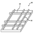
도 5 내지 도 10은 본 발명의 일 실시예에 따른 도전 패턴의 배치 방법에 의하여 형성한 도전 패턴을 예시적으로 도시하는 도면들이다.5 to 10 are views showing exemplary conductive patterns formed by a method of arranging conductive patterns according to an embodiment of the present invention.
도 5는 실험예1로서, 설정 피치 표준편차가 0에서 형성된 도전 패턴이다. 도 6은 실험예2로서, 설정 피치 표준편차가 0.13에서 형성된 도전 패턴이다. 도 7은 실험예4로서, 설정 피치 표준편차가 0.27에서 형성된 도전 패턴이다. 도 8은 실험예5로서, 설정 피치 표준편차가 0.40에서 형성된 도전 패턴이다. 도 9는 실험예6로서, 설정 피치 표준편차가 0.53에서 형성된 도전 패턴이다. 도 10는 실험예7로서, 설정 피치 표준편차가 1.06에서 형성된 도전 패턴이다. Fig. 5 shows a conductive pattern formed in Experimental Example 1 with a set pitch standard deviation of 0. Fig. Fig. 6 shows a conductive pattern formed in Experimental Example 2 with a set pitch standard deviation of 0.13. Fig. 7 shows a conductive pattern formed in Experimental Example 4 with a set pitch standard deviation of 0.27. 8 is a conductive pattern formed in Experimental Example 5 with a set pitch standard deviation of 0.40. Fig. 9 shows a conductive pattern formed at Experiment Example 6 with a set pitch standard deviation of 0.53. 10 is a conductive pattern formed at Experiment Example 7 with a set pitch standard deviation of 1.06.
도 5 내지 도 10을 참조하면, 도 5의 도전 패턴은 규칙적으로 배열되어 있다. 반면, 하기의 도 6 내지 도 10의 도전 패턴들은 불규칙적으로 배열되어 있다. 또한, 도 5의 경우에서 설정 피치 표준편차가 0인 경우(실험예1)는 도전 패턴 내의 사각형들이 동일한 크기를 가지는 규칙성을 보이는 반면, 도 6 내지 도 10의 경우에서 설정 피치 표준편차의 크기가 증가될수록 불규칙성을 더 크게 나타낸다.Referring to Figs. 5 to 10, the conductive patterns of Fig. 5 are regularly arranged. On the other hand, the conductive patterns shown in Figs. 6 to 10 are irregularly arranged. In the case of FIG. 5, the quadrangles in the conductive pattern have the same size and regularity in the case where the standard deviation of the set pitch is 0 (Experimental Example 1). On the other hand, in the cases of FIGS. 6 to 10, The greater the irregularity.
이어서, 상기 사각형 면적 값들로부터 사각형 면적 평균과 사각형 면적 표준편차를 산출하고, 상기 사각형 면적 평균값에 대한 상기 사각형 면적 표준편차의 비율을 산출하였다.Then, a square area average and a square area standard deviation were calculated from the square area values, and a ratio of the square area standard deviation to the square area average value was calculated.
이어서, 형성한 도전 패턴들을 C언어를 이용한 시뮬레이션을 통해 각각의 도전 패턴들에 의한 시인성(visibility) 수치를 얻었다.Then, the visibility value of each of the conductive patterns was obtained through simulation using the C language.
표 2는 본 발명의 일 실시예에 따른 도전 패턴의 배치 방법을 이용하여 형성한 도전 패턴의 사각형 면적 평균값, 사각형 면적 표준편차, 상기 사각형 면적 평균에 대한 상기 사각형 면적 표준편차의 비율, 및 시인성을 나타내는 표이다.Table 2 shows the square area average value, the square area standard deviation, the ratio of the square area standard deviation to the square area average, and the visibility of the conductive pattern formed using the conductive pattern arrangement method according to the embodiment of the present invention Respectively.
도 11은 본 발명의 일 실시예에 따른 도전 패턴의 배치 방법을 이용하여 형성한 도전 패턴의 상기 사각형 면적 평균에 대한 상기 사각형 면적 표준편차의 비율에 대한 시인성 변화를 나타내는 그래프이다.11 is a graph showing a change in visibility of the conductive pattern formed using the conductive pattern arranging method according to an embodiment of the present invention with respect to the ratio of the square area standard deviation to the square area average.
도 11을 참조하면, 상기 사각형 면적 표준편차가 0인 경우인 실험예1이 시인성 수치가 가장 높게 나타났고, 상기 사각형 면적 표준편차가 0이 아닌 경우에는 시인성 수치가 실험예1에 비하여 감소되었다.11, the visibility value of Experimental Example 1 in which the square area standard deviation is 0 is the highest, and in the case where the square area standard deviation is not 0, the visibility value is decreased as compared with Experimental Example 1.
시인성 수치를 기준으로 분석하면, 상기 사각형 면적 평균에 대한 상기 사각형 면적 표준편차의 비율이 예를 들어 0 초과 내지 1 이하의 범위에서 실험예1에 비하여 시인성 수치가 감소되므로, 모아레 현상을 방지할 수 있고, 도전 패턴에 의한 시인성을 감소시키는 시인성 개선을 제공할 수 있다. 바람직하게는, 상기 비율이 0.1 이상 내지 0.5 이하의 범위에서 시인성 수치가 더 감소될 수 있으므로, 시인성 개선을 더 제공할 수 있다. 또한, 더욱 바람직하게는, 상기 비율이 0.2 이상 내지 0.4 이하의 범위에서 시인성 수치가 더 감소될 수 있으므로, 시인성 개선을 더 제공할 수 있다. 가장 우수한 시인성 개선은 실험예4에서 나타났으며, 비율 0.25에서 0.04798의 시인성을 나타났다.Analysis on the basis of the visibility value shows that the visibility value is reduced in the range of the square area standard deviation with respect to the square area average, for example, in the range of more than 0 and less than 1 in comparison with Experimental Example 1, And it is possible to provide an improvement in visibility which reduces the visibility due to the conductive pattern. Preferably, the visibility value can be further reduced in the range of 0.1 or more to 0.5 or less, so that further improvement in visibility can be provided. More preferably, the visibility value can be further reduced in the range of 0.2 or more to 0.4 or less, so that it is possible to further improve the visibility. The best visibility improvement was shown in Experimental Example 4, with a visibility of 0.25 to 0.04798.
사각형 면적 표준편차가 가장 작은 실험예1의 경우에는 도전 패턴 자체에 의한 시인성은 작은 반면, 모아레 현상이 크게 나타난다. 반면, 사각형 면적 표준편차가 가장 큰 실험예7의 경우에는 모아레 현상이 감소되는 반면, 도전 패턴 자체에 의한 시인성이 크게 나타난다. 따라서, 사각형 면적 표준편차가 실험예1과 실험예7 사이에 위치하는 실험예2 내지 실험예6은 상호 배타적인, 도전 패턴에 의한 시인성의 증감과 모아레 현상의 증감에 따라 전체 시인성을 가질 수 있다.In the case of Experimental Example 1 in which the square area standard deviation is the smallest, the visibility due to the conductive pattern itself is small, whereas the moiré phenomenon is large. On the other hand, in the case of Experimental Example 7 in which the standard area standard deviation of the square is largest, the moire phenomenon is reduced, but the visibility by the conductive pattern itself is large. Thus, in Experimental Examples 2 to 6 in which the square area standard deviation is between Experimental Example 1 and Experimental Example 7, mutual exclusiveness can be obtained by increasing or decreasing the visibility due to the conductive pattern and increasing or decreasing the moire phenomenon .
이하에서는, 본 발명의 일 실시예에 따른 도전 패턴의 배치 방법을 이용하여 형성한 도전 패턴 구조체들에 대하여 설명하기로 한다. 그러나, 이러한 도전 패턴 구조체들은 예시적이며, 본 발명의 기술적 사상은 이에 한정되는 것은 아니다.Hereinafter, the conductive pattern structures formed using the conductive pattern arranging method according to an embodiment of the present invention will be described. However, these conductive pattern structures are exemplary, and the technical idea of the present invention is not limited thereto.
도 12는 본 발명의 일 실시예에 따른 도전 패턴의 배치 방법을 이용하여 형성한 도전 패턴 구조체(100)를 도시하는 사시도이다.FIG. 12 is a perspective view showing a
도 12를 참조하면, 도전 패턴 구조체(100)는 복수의 제1 도전 라인들(120)을 포함하는 제1 도전 패턴층(110), 복수의 제2 도전 라인들(130)을 포함하는 제2 도전 패턴층(150), 제1 도전 패턴층(110)과 제2 도전 패턴층(150) 사이에 위치하고 제1 도전 패턴층(110)과 제2 도전 패턴층(150)을 절연하는 절연층(190)을 포함한다. 제1 도전 라인들(120)과 제2 도전 라인들(130)의 조합에 의하여 도전 패턴이 형성될 수 있다.Referring to FIG. 12, the
제1 도전 라인들(120)은 서로 평행할 수 있다. 제2 도전 라인들(130)은 제1 도전 라인들(120)과는 일정한 각도를 가지고 서로 평행할 수 있다. 제1 도전 라인들(120)과 제2 도전 라인들(130)은 절연층(190)을 사이에 두고 이격되어 서로 교차할 수 있다. 상기 일정한 각도는 0 도 초과 내지 90 도 이하의 범위의 각도일 수 있고, 예를 들어 90 도일 수 있다.The first
상술한 바와 같이, 제1 도전 라인들(120)과 제2 도전 라인들(130)은 본 발명의 기술적 사상에 따른 도전 패턴의 배치 방법을 이용하여 배치될 수 있다. 제1 도전 라인들(120)과 제2 도전 라인들(130)에 의하여 이루어지는 사각형들의 사각형 면적 평균과 사각형 면적 표준편차의 비율은, 예를 들어 0 초과 내지 1 이하의 범위일 수 있고, 예를 들어 0.1 이상 내지 0.5 이하의 범위일 수 있고, 예를 들어 0.2 이상 내지 0.4 이하의 범위일 수 있다. 상기 사각형은 서로 마주보는 변들이 서로 평행하도록 구성될 수 있고, 예를 들어 평행사변형, 마름모, 직사각형, 또는 정사각형을 포함할 수 있다.As described above, the first
제1 도전 라인들(120)과 제2 도전 라인들(130)은 도전성 물질을 포함할 수 있고, 예를 들어 금속을 포함하거나, 예를 들어 구리, 알루미늄, 은, 금, 주석, 니켈, 크롬, 티타늄, 몰리브덴, 아연, 철, 또는 이들의 합금을 포함하거나, ITO(indium-tin oxide)와 같은 도전성 산화물을 포함할 수 있다.The first
도전 패턴 구조체(100)는 상술한 도전 라인들로 구성된 도전 패턴을 포함하는 구성요소를 의미하는 것으로서, 전자 장치에 다양한 부품으로 응용될 수 있고, 예를 들어 터치스크린 패널의 구성요소로서 응용될 수 있다.The
제1 도전 패턴층(110)과 제2 도전 패턴층(150)은 제1 도전 라인들(120)과 제2 도전 라인들(130)을 각각 탑재하는 구성요소로서, 절연성 물질을 포함할 수 있으며, 그러나, 선택적이며 생략될 수 있다. 절연층(190)은 제1 도전 라인들(120)과 제2 도전 라인들(130)을 전기적으로 절연하는 구성요소로서, 절연성 물질을 포함할 수 있으며, 다양한 형상을 가질 수 있고, 도시된 바와 같이 전체적으로 판형으로 형성되거나 또는 제1 도전 라인들(120)과 제2 도전 라인들(130)의 교차지점에 국한하여 형성될 수 있다.The first
도 13은 본 발명의 일 실시예에 따른 도전 패턴의 배치 방법을 이용하여 형성한 도전 패턴 구조체(200)를 도시하는 사시도이다. FIG. 13 is a perspective view showing a
도 13을 참조하면, 도전 패턴 구조체(200)는 제1 도전 패턴층(210), 제2 도전 패턴층(250), 및 제1 도전 패턴층(210)과 제2 도전 패턴층(250) 사이에 위치하고 제1 도전 패턴층(210)과 제2 도전 패턴층(250)을 절연하는 절연층(290)을 포함한다.Referring to FIG. 13, the
제1 도전 패턴층(210)은 복수의 제1 도전 라인들(220)과 복수의 제2 도전 라인들(230)을 포함할 수 있다. 제1 도전 라인들(220)과 제2 도전 라인들(230)의 조합에 의하여 도전 패턴이 형성될 수 있다. 제1 도전 라인들(220)과 제2 도전 라인들(230)은 제1 메쉬형 도전 패턴을 형성하도록 서로 접촉하여 교차할 수 있다.The first
제1 도전 라인들(220)은 서로 평행할 수 있다. 제2 도전 라인들(230)은 제1 도전 라인들(220)과는 일정한 각도를 가지고 서로 평행할 수 있다. 상기 일정한 각도는 0 도 초과 내지 90 도 이하의 범위의 각도일 수 있고, 예를 들어 90 도일 수 있다.The first
상술한 바와 같이, 제1 도전 라인들(220)과 제2 도전 라인들(230)은 본 발명의 기술적 사상에 따른 도전 패턴의 배치 방법을 이용하여 배치될 수 있다. 제1 도전 라인들(220)과 제2 도전 라인들(230)에 의하여 이루어지는 사각형들의 사각형 면적 평균과 사각형 면적 표준편차의 비율은, 예를 들어 0 초과 내지 1 이하의 범위일 수 있고, 예를 들어 0.1 이상 내지 0.5 이하의 범위일 수 있고, 예를 들어 0.2 이상 내지 0.4 이하의 범위일 수 있다. 상기 사각형은 서로 마주보는 변들이 서로 평행하도록 구성될 수 있고, 예를 들어 평행사변형, 마름모, 직사각형, 또는 정사각형을 포함할 수 있다.As described above, the first
제2 도전 패턴층(250)은 복수의 제3 도전 라인들(260)과 복수의 제4 도전 라인들(270)을 포함할 수 있다. 제3 도전 라인들(260)과 제4 도전 라인들(270)의 조합에 의하여 도전 패턴이 형성될 수 있다. 제3 도전 라인들(260)과 제4 도전 라인들(270)은 제2 메쉬형 도전 패턴을 형성하도록 서로 접촉하여 교차할 수 있다.The second
제1 도전 라인들(220)과 제2 도전 라인들(230)에 의하여 형성된 상기 제1 메쉬형 도전 패턴과 제3 도전 라인들(260)과 제4 도전 라인들(270)에 의하여 형성된 상기 제2 메쉬형 도전 패턴은 동일한 패턴 배열을 가질 수 있고, 동일한 방위로 배치되거나 또는 다른 방위로 배치될 수 있다. 또한, 상기 제1 메쉬형 도전 패턴과 상기 제2 메쉬형 도전 패턴은 다른 패턴 배열을 가질 수 있고, 동일한 방위로 배치되거나 또는 다른 방위로 배치될 수 있다.The first mesh-type conductive pattern formed by the first
제1 도전 라인들(220), 제2 도전 라인들(230), 제3 도전 라인들(260), 및 제4 도전 라인들(270)은 도전성 물질을 포함할 수 있고, 예를 들어 금속을 포함하거나, 예를 들어 구리, 알루미늄, 은, 금, 주석, 니켈, 크롬, 티타늄, 몰리브덴, 아연, 철, 또는 이들의 합금을 포함하거나, ITO(indium-tin oxide)와 같은 도전성 산화물을 포함할 수 있다.The first
제1 도전 패턴층(210)과 제2 도전 패턴층(250)은 절연층(290)을 사이에 두고 이격되어 서로 교차할 수 있다. The first
도전 패턴 구조체(200)는 상술한 도전 라인들로 구성된 도전 패턴을 포함하는 구성요소를 의미하는 것으로서, 전자 장치에 다양한 부품으로 응용될 수 있고, 예를 들어 터치스크린 패널의 구성요소로서 응용될 수 있다.The
제1 도전 패턴층(210)은 제1 도전 라인들(220)과 제2 도전 라인들(230)을 탑재하는 구성요소이고, 제2 도전 패턴층(250)은 제3 도전 라인들(260)과 제4 도전 라인들(270)을 각각 탑재하는 구성요소로서, 절연성 물질을 포함할 수 있으며, 그러나, 선택적이며 생략될 수 있다. 절연층(290)은 상기 제1 메쉬형 도전 패턴과 상기 제2 메쉬형 도전 패턴을 전기적으로 절연하는 구성요소로서, 절연성 물질을 포함할 수 있으며, 다양한 형상을 가질 수 있고, 도시된 바와 같이 전체적으로 판형으로 형성되거나 또는 상기 제1 메쉬형 도전 패턴과 상기 제2 메쉬형 도전 패턴의 교차지점에 국한하여 형성될 수 있다.The first
도 14는 본 발명의 일 실시예에 따른 도전 패턴의 배치 방법을 이용하여 형성한 도전 패턴 구조체(300)를 도시하는 평면도이다.FIG. 14 is a plan view showing a
도 14를 참조하면, 도전 패턴 구조체(300)는 도전 영역(302)과 도전 영역(302) 사이에 배치된 절연 영역(304)을 포함한다. 14, a
도전 영역(302)은 복수의 제1 도전 라인들(320)과 복수의 제2 도전 라인들(330)을 포함한다. 제1 도전 라인들(320)과 제2 도전 라인들(330)의 조합에 의하여 도전 패턴이 형성될 수 있다.The
제1 도전 라인들(320)은 서로 평행할 수 있다. 제2 도전 라인들(330)은 제1 도전 라인들(320)과는 일정한 각도를 가지고 서로 평행할 수 있다. 제1 도전 라인들(320)과 제2 도전 라인들(330)은 메쉬형 도전 패턴을 형성하도록 서로 접촉하여 교차할 수 있다. 상기 일정한 각도는 0 도 초과 내지 90 도 이하의 범위의 각도일 수 있고, 예를 들어 90 도일 수 있다.The first
상술한 바와 같이, 제1 도전 라인들(320)과 제2 도전 라인들(330)은 본 발명의 기술적 사상에 따른 도전 패턴의 배치 방법을 이용하여 배치될 수 있다. 제1 도전 라인들(320)과 제2 도전 라인들(330)에 의하여 이루어지는 사각형들의 사각형 면적 평균과 사각형 면적 표준편차의 비율은, 예를 들어 0 초과 내지 1 이하의 범위일 수 있고, 예를 들어 0.1 이상 내지 0.5 이하의 범위일 수 있고, 예를 들어 0.2 이상 내지 0.4 이하의 범위일 수 있다. 상기 사각형은 서로 마주보는 변들이 서로 평행하도록 구성될 수 있고, 예를 들어 평행사변형, 마름모, 직사각형, 또는 정사각형을 포함할 수 있다.As described above, the first
제1 도전 라인들(320) 및 제2 도전 라인들(330)은 도전성 물질을 포함할 수 있고, 예를 들어 금속을 포함하거나, 예를 들어 구리, 알루미늄, 은, 금, 주석, 니켈, 크롬, 티타늄, 몰리브덴, 아연, 철, 또는 이들의 합금을 포함하거나, ITO(indium-tin oxide)와 같은 도전성 산화물을 포함할 수 있다.The first
도전 영역(302)은, 예를 들어 도전 경로를 제공하는 기능을 수행할 수 있고, 예를 들어 전극을 제공할 수 있다.The
도전 패턴 구조체(300)는 상술한 도전 라인들로 구성된 도전 패턴을 포함하는 구성요소를 의미하는 것으로서, 전자 장치에 다양한 부품으로 응용될 수 있고, 예를 들어 터치스크린 패널의 구성요소로서 응용될 수 있다.The
이하에서는, 본 발명의 일 실시예에 따른 도전 패턴의 배치 방법을 이용하여 형성한 도전 패턴 구조체의 응용에 대하여 설명하기로 한다. 그러나, 이러한 도전 패턴 구조체의 응용은 예시적이며, 본 발명의 기술적 사상은 이에 한정되는 것은 아니다.Hereinafter, the application of the conductive pattern structure formed using the conductive pattern arranging method according to an embodiment of the present invention will be described. However, the application of such a conductive pattern structure is illustrative, and the technical idea of the present invention is not limited thereto.
도 15는 본 발명의 일 실시예에 따른 도전 패턴의 배치 방법을 이용하여 형성한 도전 패턴 구조체를 포함하는 도전성 매쉬(400)를 도시하는 평면도이다.15 is a plan view showing a
도 15를 참조하면, 도전성 매쉬(400)는 서로 평행한 복수의 제1 도전 라인들(420); 및 상기 제1 도전 라인들(420)과는 일정한 각도를 가지고 서로 평행한 복수의 제2 도전 라인들(430);을 포함할 수 있다. 제1 도전 라인들(420)과 제2 도전 라인들(430)에 의하여 이루어지는 사각형들의 사각형 면적 평균과 사각형 면적 표준편차의 비율은, 예를 들어 0 초과 내지 1 이하의 범위일 수 있고, 예를 들어 0.1 이상 내지 0.5 이하의 범위일 수 있고, 예를 들어 0.2 이상 내지 0.4 이하의 범위일 수 있다.Referring to FIG. 15, the
도전성 매쉬(400)는 도전성 물질을 포함할 수 있고, 예를 들어 금속을 포함하거나, 예를 들어 예를 들어 구리, 알루미늄, 은, 금, 주석, 니켈, 크롬, 티타늄, 몰리브덴, 아연, 철, 또는 이들의 합금을 포함할 수 있다. 또한, 제1 도전 라인들(420)과 제2 도전 라인들(430)은 상술한 도전 패턴 구조체를 구성할 수 있다. The
도 16은 본 발명의 일 실시예에 따른 도전 패턴의 배치 방법을 이용하여 형성한 도전 패턴 구조체를 구현하는 포토마스크(500)를 도시하는 평면도이다.16 is a plan view showing a
도 16을 참조하면, 포토마스크(500)는 서로 평행한 복수의 제1 패턴 라인들(520); 및 상기 제1 패턴 라인들(520)과는 일정한 각도를 가지고 서로 평행한 복수의 제2 패턴 라인들(530);을 포함할 수 있다. 제1 패턴 라인들(520)과 제2 패턴 라인들(530)에 의하여 이루어지는 사각형들의 사각형 면적 평균과 사각형 면적 표준편차의 비율은, 예를 들어 0 초과 내지 1 이하의 범위일 수 있고, 예를 들어 0.1 이상 내지 0.5 이하의 범위일 수 있고, 예를 들어 0.2 이상 내지 0.4 이하의 범위일 수 있다.Referring to FIG. 16, the
포토마스크(500)는 투명한 물질을 포함할 수 있고, 예를 들어 유리, 플라스틱, 석영 등을 포함할 수 있다. 제1 패턴 라인들(520)과 제2 패턴 라인들(530) 각각은 상술한 상기 제1 도전 라인들과 상기 제2 도전 라인들 각각을 형성하기 위한 포토마스크(500) 상의 구성요소일 수 있다. 제1 패턴 라인들(520)과 제2 패턴 라인들(530) 각각은 상술한 제1 도전 라인들과 제2 도전 라인들 각각에 대응하는 형상을 가질 수 있다.The
도 17은 본 발명의 일 실시예에 따른 도전 패턴의 배치 방법을 이용하여 형성한 도전 패턴 구조체를 구현하는 스템퍼(600)를 도시하는 평면도이다.17 is a plan view showing a
도 17을 참조하면, 스템퍼(600)는 서로 평행한 복수의 제1 패턴 라인들(620); 및 상기 제1 패턴 라인들(620)과는 일정한 각도를 가지고 서로 평행한 복수의 제2 패턴 라인들(630);을 포함할 수 있다. 제1 패턴 라인들(620)과 제2 패턴 라인들(630)에 의하여 이루어지는 사각형들의 사각형 면적 평균과 사각형 면적 표준편차의 비율은, 예를 들어 0 초과 내지 1 이하의 범위일 수 있고, 예를 들어 0.1 이상 내지 0.5 이하의 범위일 수 있고, 예를 들어 0.2 이상 내지 0.4 이하의 범위일 수 있다.17, the
스템퍼(600)는 유리, 수정, 고무, 실리콘, 폴리머 등을 포함할 수 있다. 제1 패턴 라인들(620)과 제2 패턴 라인들(630) 각각은 상술한 상기 제1 도전 라인들과 상기 제2 도전 라인들 각각을 형성하기 위한 스템퍼(600) 상의 구성요소일 수 있다. 제1 패턴 라인들(620)과 제2 패턴 라인들(630) 각각은 돌출된 형상을 가질 수 있다. 제1 패턴 라인들(620)과 제2 패턴 라인들(630) 각각은 상술한 제1 도전 라인들과 제2 도전 라인들 각각에 대응하는 형상을 가질 수 있다.The
이하에서는, 본 발명의 일 실시예에 따른 도전 패턴의 배치 방법을 이용하여 형성한 도전 패턴 구조체를 적용한 전자 장치에 대하여 설명하기로 한다. 상기 전자 장치로서 예시적으로 디스플레이 장치를 설명한다. 또한, 도전 패턴 구조체는 디스플레이 장치 내의 터치 스크린 패널에 적용된 경우에 대하여 설명한다.Hereinafter, an electronic device to which a conductive pattern structure formed using a conductive pattern arranging method according to an embodiment of the present invention is applied will be described. A display device will be described as an example of the electronic device. The conductive pattern structure is applied to a touch screen panel in a display device.
도 18은 본 발명의 일 실시예에 따른 도전 패턴 구조체들을 가지는 터치 스크린 패널이 적용된 디스플레이 장치(700)를 나타내는 도면이다.18 is a view illustrating a
도 18을 참조하면, 디스플레이 장치(700)는 하나 또는 그 이상의 조작부(710), 카메라(720), 스피커(730), 마이크(미도시), 및 터치 스크린 패널(740)을 구비한다. 디스플레이 장치(700)는 어플리케이션을 실행하거나 컨텐츠를 표시 가능하도록 구성되는 장치로써, 예를 들어, 태블릿(Tablet) 개인 컴퓨터(Personal Computer: PC), 휴대용 멀티미디어 재생 장치(Portable Multimedia Player: PMP), 개인 정보 단말기(Personal Digital Assistant: PDA), 스마트 폰(Smart Phone), 휴대폰, 디지털 액자 등을 포함할 수 있다. 18, the
여기에서, 터치 스크린 패널(740)은 본 발명의 기술적 사상에 따른 도전 패턴 구조체들을 포함하여 구성될 수 있다. 구체적으로, 터치 스크린 패널(740)은 서로 평행한 복수의 제1 도전 라인들; 및 상기 제1 도전 라인들과는 일정한 각도를 가지고 서로 평행한 복수의 제2 도전 라인들;을 포함할 수 있다. 여기에서, 상기 제1 도전 라인들과 상기 제2 도전 라인들에 의하여 이루어지는 사각형들의 사각형 면적 평균과 사각형 면적 표준편차의 비율은, 예를 들어 0 초과 내지 1 이하의 범위일 수 있고, 예를 들어 0.1 이상 내지 0.5 이하의 범위일 수 있고, 예를 들어 0.2 이상 내지 0.4 이하의 범위일 수 있다.Here, the
도 19는 본 발명의 일 실시예에 따른 도전 패턴의 배치 방법을 수행하는 시스템(1000)을 도시하는 개략도이다.19 is a schematic diagram showing a
도 19를 참조하면, 본 발명의 일부 실시예들에 따른 도전 패턴의 배치 방법을 수행하기 컴퓨터 시스템(1300)은 일반적인 목적으로 사용되는 워크스테이션일 수 있다. 컴퓨터 시스템(1300)은 단독형(stand alone) 또는 네트워크 형일 수 있으며, 연산을 위한 싱글 또는 멀티 프로세서를 포함할 수 있으며, 병렬 처리 컴퓨터 시스템일 수 있다.Referring to FIG. 19, the
컴퓨터 시스템(1300)은 프로그램 저장 매체(1100), 예를 들면 컴팩트 디스크(CD), 디지털 비디오 디스크(DVD), USB 저장 매체, 고상 디스크(SSD)에 기록되어 있거나, 인터넷과 같은 유무선 통신망을 통하여 전달되는 실행 가능한 일련의 명령을 수행한다. 컴퓨터 시스템(1300)은 상술한 도전 패턴의 배치에 관한 정보를 저장하는 파일 저장소(1200), 예를 들면, 데이터베이스 또는 다른 저장 매체로부터 도전 패턴의 배치에 관한 정보가 담긴 파일을 제공받아 이를 독출하는 명령을 수행한다. 컴퓨터 시스템(1300)은 도전 패턴의 배치에 대하여 본 발명의 일부 실시예들에 따른 제1 도전 라인들과 제2 도전 라인들로 이루어지는 도전 패턴의 배치를 종료한 후, 상기 처리에 관한 정보가 담긴 파일을 생성한다. 이어서, 도전 패턴의 배치는 기록 장치(1400)에 전달되고, 이에 의해 도전 패턴이 제조된다.The
시스템(1000)은 제1 설정 피치 평균과 제1 설정 피치 표준편차를 설정하는 제1 설정 메커니즘; 상기 제1 설정 피치 평균과 상기 제1 설정 피치 표준편차를 이용하여, 서로 평행한 복수의 제1 도전 라인들을 배치하는 제1 배치 메커니즘; 제2 설정 피치 평균과 제2 설정 피치 표준편차를 설정하는 제2 설정 메커니즘; 및 상기 제2 설정 피치 평균과 상기 제2 설정 피치 표준편차를 이용하여, 상기 제1 도전 라인들과는 일정한 각도를 가지고 서로 평행한 복수의 제2 도전 라인들을 배치하는 제2 배치 메커니즘;을 포함할 수 있다. 또한, 선택적으로(optionally), 시스템(1000)은, 상기 제1 도전 라인들과 상기 제2 도전 라인들에 의하여 이루어지는 사각형 면적 값들을 산출하는 제1 산출 메커니즘; 상기 사각형 면적 값들로부터 사각형 면적 평균과 사각형 면적 표준편차를 산출하는 제2 메커니즘; 상기 사각형 면적 평균에 대한 상기 사각형 면적 표준편차의 비율을 산출하는 제3 산출 메커니즘; 상기 비율이 허용 비율 범위 내에 포함되는지 여부를 판단하는 판단 메커니즘; 및 상기 판단하는 단계에서 상기 비율이 허용 비율 범위 내의 포함되는 경우에는, 상기 제1 도전 라인들과 상기 제2 도전 라인들로 이루어지는 도전 패턴의 배치를 종료하는 종료 메커니즘;을 더 포함할 수 있다. 또한, 선택적으로(optionally), 시스템(1000)은, 상기 판단하는 단계에서 상기 비율이 상기 허용 비율 범위 내의 포함되지 않는 경우에는, 상기 제1 설정 피치 평균과 제1 설정 피치 표준편차를 설정하는 단계로 되돌아가는 피드백 메커니즘을 더 포함할 수 있다.The
상기한 본 발명의 기술적 사상은 또한 컴퓨터에서 판독 가능한 저장 매체에 컴퓨터가 읽을 수 있는 코드로서 구현하는 것이 가능하다. 컴퓨터에서 판독 가능한 저장 매체는 컴퓨터 시스템에 의하여 판독 가능한 데이터가 저장되는 모든 종류의 저장장치를 포함한다. 컴퓨터에서 판독 가능한 저장 매체의 예로는 ROM, RAM, CD-ROM, DVD, 자기 테이프, 플로피디스크, 광데이터 저장장치, 플래시 메모리, 고상 디스크(solid state disk 등이 있으며, 또한 캐리어 웨이브(예를 들어 인터넷을 통한 전송)의 형태로 구현되는 것도 포함한다. 또한 컴퓨터에서 판독 가능한 저장 매체는 네트워크로 연결된 컴퓨터 시스템에 분산되어, 분산방식으로 컴퓨터에서 판독 가능한 코드가 저장되고 실행될 수 있다. 여기서, 저장 매체에 저장되는 프로그램 또는 코드라 함은 특정한 결과를 얻기 위하여 컴퓨터 등이 정보처리능력을 갖는 장치 내에서 직접적 또는 간접적으로 사용되는 일련의 지시 명령으로 표현된 것을 의미한다. 따라서, 컴퓨터라는 용어도 실제 사용되는 명칭에 여하를 불구하고 메모리, 입출력장치, 연산장치를 구비하여 프로그램에 의하여 특정의 기능을 수행하기 위한 정보처리능력을 가진 모든 장치를 총괄하는 의미로 사용된다. 상기 저장 매체는, 도전 패턴의 배치 방법을 컴퓨터에서 수행시킬 때, 상기 각 단계들을 수행하도록 하는 프로그래밍된 명령을 저장할 수 있다. The technical idea of the present invention described above can also be embodied as computer-readable code on a computer-readable storage medium. A computer-readable storage medium includes any kind of storage device in which data readable by a computer system is stored. Examples of computer-readable storage media include ROM, RAM, CD-ROM, DVD, magnetic tape, floppy disk, optical data storage, flash memory, solid state disk, The computer-readable storage medium may also be distributed over a network-connected computer system so that the computer-readable code may be stored and executed in a distributed manner. Means that a computer or the like is represented by a series of instructions that are used directly or indirectly in an apparatus having an information processing capability in order to obtain a specific result. Despite its name, it has a memory, an input / output device, The storage medium may be programmed to perform the respective steps when performing a method of arranging a conductive pattern in a computer, You can save the command.
이상에서 설명한 본 발명의 기술적 사상이 전술한 실시예 및 첨부된 도면에 한정되지 않으며, 본 발명의 기술적 사상을 벗어나지 않는 범위 내에서 여러 가지 치환, 변형 및 변경이 가능하다는 것은, 본 발명의 기술적 사상이 속하는 기술분야에서 통상의 지식을 가진 자에게 있어 명백할 것이다.It will be apparent to those skilled in the art that various modifications and variations can be made in the present invention without departing from the spirit or scope of the invention as defined in the appended claims. Will be apparent to those of ordinary skill in the art.
100: 도전 패턴 구조체, 110: 제1 도전 패턴층
120: 제1 도전 라인들, 130: 제2 도전 라인들
150: 제2 도전 패턴층, 190: 절연층
200: 도전 패턴 구조체, 210: 제1 도전 패턴층
220: 제1 도전 라인들, 230: 제2 도전 라인들
250: 제2 도전 패턴층, 260: 제3 도전 라인들
270: 제4 도전 라인들, 290: 절연층
300: 도전 패턴 구조체, 302: 도전 영역
304: 절연 영역, 320: 제1 도전 라인들
330: 제2 도전 라인들, 400: 도전성 매쉬
420: 제1 도전 라인들, 430: 제2 도전 라인들
500: 도전성 매쉬, 520: 제1 패턴 라인들
530: 제2 패턴 라인들, 600: 스템퍼
620: 제1 패턴 라인들, 630: 제2 패턴 라인들
700: 디스플레이 장치, 710: 조작부
720: 카메라, 730: 스피커
740: 터치 스크린 패널, 1000: 시스템
1100: 프로그램 저장 매체, 1200: 파일 저장소
1300: 컴퓨터 시스템, 1400: 기록 장치100: conductive pattern structure, 110: first conductive pattern layer
120: first conductive lines, 130: second conductive lines
150: second conductive pattern layer, 190: insulating layer
200: conductive pattern structure, 210: first conductive pattern layer
220: first conductive lines, 230: second conductive lines
250: second conductive pattern layer, 260: third conductive lines
270: fourth conductive lines, 290: insulating layer
300: conductive pattern structure, 302: conductive region
304: isolation region, 320: first conductive lines
330: second conductive lines, 400: conductive mesh
420: first conductive lines, 430: second conductive lines
500: conductive mesh, 520: first pattern lines
530: second pattern lines, 600: stamper
620: first pattern lines, 630: second pattern lines
700: display device, 710:
720: camera, 730: speaker
740: Touch screen panel, 1000: System
1100: program storage medium, 1200: file storage
1300: computer system, 1400: recording device
Claims (15)
상기 제1 설정 피치 평균과 상기 제1 설정 피치 표준편차를 이용하여, 서로 평행한 복수의 제1 도전 라인들을 배치하는 단계;
제2 설정 피치 평균과 제2 설정 피치 표준편차를 설정하는 단계; 및
상기 제2 설정 피치 평균과 상기 제2 설정 피치 표준편차를 이용하여, 상기 제1 도전 라인들과는 일정한 각도를 가지고 서로 평행한 복수의 제2 도전 라인들을 배치하는 단계;
를 포함하는, 도전 패턴의 배치 방법.Setting a first set pitch average and a first set pitch standard deviation;
Disposing a plurality of first conductive lines parallel to each other using the first set pitch average and the first set pitch standard deviation;
Setting a second set pitch average and a second set pitch standard deviation; And
Disposing a plurality of second conductive lines parallel to each other at an angle with the first conductive lines using the second set pitch average and the second set pitch standard deviation;
Wherein the conductive pattern is formed on the conductive pattern.
상기 복수의 제2 도전 라인들을 배치하는 단계를 수행한 후에,
상기 제1 도전 라인들과 상기 제2 도전 라인들에 의하여 이루어지는 사각형 면적 값들을 산출하는 단계;
상기 사각형 면적 값들로부터 사각형 면적 평균과 사각형 면적 표준편차를 산출하는 단계;
상기 사각형 면적 평균에 대한 상기 사각형 면적 표준편차의 비율을 산출하는 단계;
상기 비율이 허용 비율 범위 내에 포함되는지 여부를 판단하는 단계; 및
상기 판단하는 단계에서 상기 비율이 허용 비율 범위 내의 포함되는 경우에는, 상기 제1 도전 라인들과 상기 제2 도전 라인들로 이루어지는 도전 패턴의 배치를 종료하는 단계;
를 더 포함하는, 도전 패턴의 배치 방법.The method according to claim 1,
After performing the step of disposing the plurality of second conductive lines,
Calculating square area values formed by the first conductive lines and the second conductive lines;
Calculating a square area average and a square area standard deviation from the square area values;
Calculating a ratio of the square area standard deviation to the square area average;
Determining whether the ratio is within an acceptable ratio range; And
Ending the arrangement of the conductive patterns including the first conductive lines and the second conductive lines when the ratio is within the allowable ratio range in the determining step;
Further comprising the steps of:
상기 판단하는 단계에서 상기 비율이 상기 허용 비율 범위 내의 포함되지 않는 경우에는, 상기 제1 설정 피치 평균과 제1 설정 피치 표준편차를 설정하는 단계로 되돌아가는 피드백 단계;를 더 포함하는, 도전 패턴의 배치 방법.3. The method of claim 2,
And returning to the step of setting the first set pitch average and the first set pitch standard deviation if the ratio is not included within the allowable ratio range in the determining step Placement method.
상기 허용 비율 범위는 0 초과 내지 1 이하의 범위인, 도전 패턴의 배치 방법.3. The method of claim 2,
Wherein the allowable ratio range is in the range of more than 0 to 1 or less.
상기 허용 비율 범위는 0.1 이상 내지 0.5 이하의 범위인, 도전 패턴의 배치 방법.3. The method of claim 2,
Wherein the permissible ratio range is in the range of 0.1 or more to 0.5 or less.
상기 허용 비율 범위는 0.2 이상 내지 0.4 이하의 범위인, 도전 패턴의 배치 방법.3. The method of claim 2,
Wherein the allowable ratio range is in the range of 0.2 or more to 0.4 or less.
상기 제1 도전 라인들을 배치하는 단계는,
상기 제1 설정 피치 평균과 상기 제1 설정 피치 표준편차를 난수 발생기에 입력하여 복수의 제1 피치 값들을 발생시키는 단계; 및
상기 제1 도전 라인들을 상기 복수의 제1 피치 값들에 따라 배치하는 단계;를 포함하는, 도전 패턴의 배치 방법.The method according to claim 1,
Wherein disposing the first conductive lines comprises:
Inputting the first set pitch average and the first set pitch standard deviation to a random number generator to generate a plurality of first pitch values; And
And arranging the first conductive lines according to the plurality of first pitch values.
상기 제2 도전 라인들을 배치하는 단계는,
상기 제2 설정 피치 평균과 상기 제2 설정 피치 표준편차를 난수 발생기에 입력하여 복수의 제2 피치 값들을 발생시키는 단계; 및
상기 제2 도전 라인들을 상기 복수의 제2 피치 값들에 따라 배치하는 단계;를 포함하는, 도전 패턴의 배치 방법.The method according to claim 1,
Wherein the step of disposing the second conductive lines comprises:
Inputting the second set pitch average and the second set pitch standard deviation to a random number generator to generate a plurality of second pitch values; And
And arranging the second conductive lines in accordance with the plurality of second pitch values.
상기 제1 설정 피치 평균과 상기 제2 설정 피치 평균은 동일한 값을 가지고, 상기 제1 설정 피치 표준편차와 상기 제2 설정 피치 표준편차는 동일한 값을 가지는, 도전 패턴의 배치 방법.The method according to claim 1,
Wherein the first set pitch average and the second set pitch average have the same value and the first set pitch standard deviation and the second set pitch standard deviation have the same value.
상기 제1 설정 피치 평균과 상기 제2 설정 피치 평균은 동일한 값을 가지고, 상기 제1 설정 피치 표준편차와 상기 제2 설정 피치 표준편차는 동일한 값을 가지고,
상기 제2 도전 라인들을 배치하는 단계는, 상기 제1 설정 피치 평균과 상기 제1 설정 피치 표준편차를 이용하여 발생시킨 상기 복수의 제1 피치 값들을 이용하여 상기 복수의 제2 도전 라인들을 배치하는, 도전 패턴의 배치 방법.8. The method of claim 7,
Wherein the first set pitch average and the second set pitch average have the same value and the first set pitch standard deviation and the second set pitch standard deviation have the same value,
Wherein arranging the second conductive lines includes arranging the plurality of second conductive lines using the plurality of first pitch values generated using the first set pitch average and the first set pitch standard deviation , And arranging the conductive pattern.
상기 제1 도전 라인들과는 일정한 각도를 가지고 서로 평행한 복수의 제2 도전 라인들;
을 포함하고,
상기 제1 도전 라인들과 상기 제2 도전 라인들에 의하여 이루어지는 사각형들의 사각형 면적 평균과 사각형 면적 표준편차의 비율은 0 초과 내지 1 이하의 범위인, 도전 패턴 구조체.A plurality of first conductive lines parallel to each other; And
A plurality of second conductive lines parallel to each other at an angle with the first conductive lines;
/ RTI >
Wherein a ratio of a square area average of squares formed by the first conductive lines and the second conductive lines to a square area standard deviation is in a range of more than 0 and less than 1.
상기 제1 도전 라인들과 제2 도전 라인들은 이격되어 서로 교차하는, 도전 패턴 구조체.12. The method of claim 11,
Wherein the first conductive lines and the second conductive lines are spaced apart from each other.
상기 제1 도전 라인들과 제2 도전 라인들은 메쉬형 도전 패턴을 형성하도록 서로 접촉하여 교차하는, 도전 패턴 구조체.12. The method of claim 11,
Wherein the first conductive lines and the second conductive lines contact and cross each other to form a mesh-like conductive pattern.
상기 사각형은 평행사변형, 마름모, 직사각형, 또는 정사각형을 포함하는, 도전 패턴 구조체.12. The method of claim 11,
Wherein the rectangle comprises a parallelogram, a rhombus, a rectangle, or a square.
상기 일정한 각도는 0도 초과 내지 90 도 이하의 범위의 각도인, 도전 패턴 구조체.12. The method of claim 11,
Wherein the constant angle is an angle in the range of more than 0 degrees to less than 90 degrees.
Priority Applications (2)
| Application Number | Priority Date | Filing Date | Title |
|---|---|---|---|
| KR1020160132501A KR20180040792A (en) | 2016-10-13 | 2016-10-13 | Method of arranging conductive pattern, conductive pattern structure formed by using the same, conductive mesh, photomask, stamper, touch screen panel |
| PCT/KR2017/010365 WO2018070682A2 (en) | 2016-10-13 | 2017-09-21 | Conductive pattern arrangement method and conductive pattern structure, conductive mesh, photomask, stamper, and touch screen panel formed by using same method |
Applications Claiming Priority (1)
| Application Number | Priority Date | Filing Date | Title |
|---|---|---|---|
| KR1020160132501A KR20180040792A (en) | 2016-10-13 | 2016-10-13 | Method of arranging conductive pattern, conductive pattern structure formed by using the same, conductive mesh, photomask, stamper, touch screen panel |
Publications (1)
| Publication Number | Publication Date |
|---|---|
| KR20180040792A true KR20180040792A (en) | 2018-04-23 |
Family
ID=61906318
Family Applications (1)
| Application Number | Title | Priority Date | Filing Date |
|---|---|---|---|
| KR1020160132501A Ceased KR20180040792A (en) | 2016-10-13 | 2016-10-13 | Method of arranging conductive pattern, conductive pattern structure formed by using the same, conductive mesh, photomask, stamper, touch screen panel |
Country Status (2)
| Country | Link |
|---|---|
| KR (1) | KR20180040792A (en) |
| WO (1) | WO2018070682A2 (en) |
Citations (2)
| Publication number | Priority date | Publication date | Assignee | Title |
|---|---|---|---|---|
| KR20100090669A (en) * | 2009-02-06 | 2010-08-16 | 주식회사 엘지화학 | Touchscreen and method for manufacturing the same |
| KR101447927B1 (en) * | 2014-07-08 | 2014-10-13 | 주식회사 대승소재 | Touch screen panel of metal mesh structure and preparation method thereof |
Family Cites Families (3)
| Publication number | Priority date | Publication date | Assignee | Title |
|---|---|---|---|---|
| KR101328483B1 (en) * | 2012-05-10 | 2013-11-13 | 전자부품연구원 | Transparent electrode thin-film with metal mesh structure and method thereof |
| EP2985750A4 (en) * | 2013-04-10 | 2016-08-24 | Fujifilm Corp | CONDUCTIVE FILM, DISPLAY DEVICE HAVING THE SAME, AND EVALUATION AND DETERMINATION METHOD FOR A CONDUCTIVE FILM WIRING PATTERN |
| US20160133357A1 (en) * | 2014-11-11 | 2016-05-12 | Ronald Steven Cok | Providing electrically-conductive articles with electrically-conductive metallic connectors |
-
2016
- 2016-10-13 KR KR1020160132501A patent/KR20180040792A/en not_active Ceased
-
2017
- 2017-09-21 WO PCT/KR2017/010365 patent/WO2018070682A2/en not_active Ceased
Patent Citations (2)
| Publication number | Priority date | Publication date | Assignee | Title |
|---|---|---|---|---|
| KR20100090669A (en) * | 2009-02-06 | 2010-08-16 | 주식회사 엘지화학 | Touchscreen and method for manufacturing the same |
| KR101447927B1 (en) * | 2014-07-08 | 2014-10-13 | 주식회사 대승소재 | Touch screen panel of metal mesh structure and preparation method thereof |
Also Published As
| Publication number | Publication date |
|---|---|
| WO2018070682A3 (en) | 2018-08-09 |
| WO2018070682A2 (en) | 2018-04-19 |
Similar Documents
| Publication | Publication Date | Title |
|---|---|---|
| US9582131B2 (en) | Touch sensor panel design | |
| US11054936B2 (en) | Touch panel with non-uniform touch node layout | |
| US9715294B2 (en) | In-cell touch panel and manufacturing method thereof, and display device | |
| US20240134479A1 (en) | Merged floating pixels in a touch screen | |
| US10394364B2 (en) | Touch pressure sensitivity correction method and computer-readable recording medium | |
| CN112306308A (en) | Metal mesh touch electrode with visibility reduction | |
| KR101709152B1 (en) | Sensitivity compensation method of touch input device being capable of touch pressure sensing and computer readable recording medium | |
| JP2017527938A (en) | Touch panel, touch position specifying method, and display device | |
| CN105589613A (en) | Touch point location method and apparatus, and terminal device | |
| CN112558806B (en) | Spherical or highly curved touch-sensitive surface | |
| CN104331210A (en) | Embedded touch screen, and touch detection method and display device of embedded touch screen | |
| US20120242613A1 (en) | Projected capacitive touch panel | |
| CN103116431A (en) | Self-capacitance touch screen and electronic equipment | |
| CN106708307B (en) | Touch panel with metal lines without induction function | |
| KR101780260B1 (en) | Sensitivity compensation method of touch input device being capable of touch pressure sensing and computer readable recording medium | |
| CN104077000B (en) | Touch panel and its driving method, display device | |
| WO2021016762A1 (en) | Touch control electrode structure, touch screen and touch control display apparatus | |
| CN103049145A (en) | Mutual capacitive touch induction device and electronic system containing same | |
| JPWO2019021572A1 (en) | Position detection sensor, position detection device, and information processing system | |
| CN104461164A (en) | Touch display panel and touch display device | |
| KR20200023183A (en) | Input device | |
| US11620021B1 (en) | Methods and apparatus for cross-coupling correction on a touch sensor panel | |
| CN103149752B (en) | A kind of display panels and manufacture method, display device | |
| KR20180040792A (en) | Method of arranging conductive pattern, conductive pattern structure formed by using the same, conductive mesh, photomask, stamper, touch screen panel | |
| US20190302947A1 (en) | Method for correcting sensitivity of touch input device that detects touch pressure and computer-readable recording medium |
Legal Events
| Date | Code | Title | Description |
|---|---|---|---|
| A201 | Request for examination | ||
| PA0109 | Patent application |
Patent event code: PA01091R01D Comment text: Patent Application Patent event date: 20161013 |
|
| PA0201 | Request for examination | ||
| E902 | Notification of reason for refusal | ||
| PE0902 | Notice of grounds for rejection |
Comment text: Notification of reason for refusal Patent event date: 20180411 Patent event code: PE09021S01D |
|
| PG1501 | Laying open of application | ||
| E601 | Decision to refuse application | ||
| PE0601 | Decision on rejection of patent |
Patent event date: 20190221 Comment text: Decision to Refuse Application Patent event code: PE06012S01D Patent event date: 20180411 Comment text: Notification of reason for refusal Patent event code: PE06011S01I |