KR20170126560A - Display Device Having Touch Sensor - Google Patents
Display Device Having Touch Sensor Download PDFInfo
- Publication number
- KR20170126560A KR20170126560A KR1020160056628A KR20160056628A KR20170126560A KR 20170126560 A KR20170126560 A KR 20170126560A KR 1020160056628 A KR1020160056628 A KR 1020160056628A KR 20160056628 A KR20160056628 A KR 20160056628A KR 20170126560 A KR20170126560 A KR 20170126560A
- Authority
- KR
- South Korea
- Prior art keywords
- touch
- driving
- driving signal
- sensing
- period
- Prior art date
- Legal status (The legal status is an assumption and is not a legal conclusion. Google has not performed a legal analysis and makes no representation as to the accuracy of the status listed.)
- Granted
Links
Images


Classifications
-
- G—PHYSICS
- G06—COMPUTING OR CALCULATING; COUNTING
- G06F—ELECTRIC DIGITAL DATA PROCESSING
- G06F3/00—Input arrangements for transferring data to be processed into a form capable of being handled by the computer; Output arrangements for transferring data from processing unit to output unit, e.g. interface arrangements
- G06F3/01—Input arrangements or combined input and output arrangements for interaction between user and computer
- G06F3/03—Arrangements for converting the position or the displacement of a member into a coded form
- G06F3/041—Digitisers, e.g. for touch screens or touch pads, characterised by the transducing means
- G06F3/0416—Control or interface arrangements specially adapted for digitisers
-
- G—PHYSICS
- G09—EDUCATION; CRYPTOGRAPHY; DISPLAY; ADVERTISING; SEALS
- G09G—ARRANGEMENTS OR CIRCUITS FOR CONTROL OF INDICATING DEVICES USING STATIC MEANS TO PRESENT VARIABLE INFORMATION
- G09G3/00—Control arrangements or circuits, of interest only in connection with visual indicators other than cathode-ray tubes
- G09G3/20—Control arrangements or circuits, of interest only in connection with visual indicators other than cathode-ray tubes for presentation of an assembly of a number of characters, e.g. a page, by composing the assembly by combination of individual elements arranged in a matrix no fixed position being assigned to or needed to be assigned to the individual characters or partial characters
- G09G3/34—Control arrangements or circuits, of interest only in connection with visual indicators other than cathode-ray tubes for presentation of an assembly of a number of characters, e.g. a page, by composing the assembly by combination of individual elements arranged in a matrix no fixed position being assigned to or needed to be assigned to the individual characters or partial characters by control of light from an independent source
- G09G3/36—Control arrangements or circuits, of interest only in connection with visual indicators other than cathode-ray tubes for presentation of an assembly of a number of characters, e.g. a page, by composing the assembly by combination of individual elements arranged in a matrix no fixed position being assigned to or needed to be assigned to the individual characters or partial characters by control of light from an independent source using liquid crystals
- G09G3/3611—Control of matrices with row and column drivers
- G09G3/3648—Control of matrices with row and column drivers using an active matrix
-
- G—PHYSICS
- G09—EDUCATION; CRYPTOGRAPHY; DISPLAY; ADVERTISING; SEALS
- G09G—ARRANGEMENTS OR CIRCUITS FOR CONTROL OF INDICATING DEVICES USING STATIC MEANS TO PRESENT VARIABLE INFORMATION
- G09G2310/00—Command of the display device
- G09G2310/02—Addressing, scanning or driving the display screen or processing steps related thereto
- G09G2310/0264—Details of driving circuits
- G09G2310/0297—Special arrangements with multiplexing or demultiplexing of display data in the drivers for data electrodes, in a pre-processing circuitry delivering display data to said drivers or in the matrix panel, e.g. multiplexing plural data signals to one D/A converter or demultiplexing the D/A converter output to multiple columns
-
- G—PHYSICS
- G09—EDUCATION; CRYPTOGRAPHY; DISPLAY; ADVERTISING; SEALS
- G09G—ARRANGEMENTS OR CIRCUITS FOR CONTROL OF INDICATING DEVICES USING STATIC MEANS TO PRESENT VARIABLE INFORMATION
- G09G2320/00—Control of display operating conditions
- G09G2320/02—Improving the quality of display appearance
- G09G2320/0223—Compensation for problems related to R-C delay and attenuation in electrodes of matrix panels, e.g. in gate electrodes or on-substrate video signal electrodes
-
- G—PHYSICS
- G09—EDUCATION; CRYPTOGRAPHY; DISPLAY; ADVERTISING; SEALS
- G09G—ARRANGEMENTS OR CIRCUITS FOR CONTROL OF INDICATING DEVICES USING STATIC MEANS TO PRESENT VARIABLE INFORMATION
- G09G2330/00—Aspects of power supply; Aspects of display protection and defect management
- G09G2330/02—Details of power systems and of start or stop of display operation
- G09G2330/021—Power management, e.g. power saving
-
- G—PHYSICS
- G09—EDUCATION; CRYPTOGRAPHY; DISPLAY; ADVERTISING; SEALS
- G09G—ARRANGEMENTS OR CIRCUITS FOR CONTROL OF INDICATING DEVICES USING STATIC MEANS TO PRESENT VARIABLE INFORMATION
- G09G2330/00—Aspects of power supply; Aspects of display protection and defect management
- G09G2330/06—Handling electromagnetic interferences [EMI], covering emitted as well as received electromagnetic radiation
Landscapes
- Engineering & Computer Science (AREA)
- Theoretical Computer Science (AREA)
- Physics & Mathematics (AREA)
- General Physics & Mathematics (AREA)
- General Engineering & Computer Science (AREA)
- Chemical & Material Sciences (AREA)
- Crystallography & Structural Chemistry (AREA)
- Computer Hardware Design (AREA)
- Human Computer Interaction (AREA)
- Position Input By Displaying (AREA)
- Control Of Indicators Other Than Cathode Ray Tubes (AREA)
Abstract
본 발명에 의한 터치 센서 내장형 표시장치는 표시패널, 표시패널 구동회로부 및 터치 구동회로부를 포함한다. 표시패널에는 픽셀 어레이 내에 배치된 터치 센서들 및 터치 센서들과 연결되는 센싱 라인들이 배열되며, 픽셀 구동기간 및 터치 구동기간으로 시분할 구동된다. 표시패널 구동회로부는 픽셀 어레이의 픽셀들에 영상 데이터를 기입한다. 터치 구동회로부는 센싱 라인들을 통해 터치 센서들에 교류 파형인 터치블록 구동신호를 공급하고, 센싱 라인들을 통해 감지된 터치 센서들의 전하 변화량을 바탕으로 터치 입력을 판단한다. 터치 구동 구동회로부는 매 프레임의 터치 구동기간 동안에, 제1 내지 제k(k는 자연수) 터치블록 구동신호를 생성하여 제1 내지 제k 터치블록을 순차적으로 구동한다. 제k 터치기간 동안에 출력되는 제k 터치블록 구동신호는 제k 터치기간 이외에 출력되는 교류신호의 스윙폭이 제k 터치기간 동안에 출력되는 교류신호의 스윙폭보다 작게 제어된다.A touch sensor built-in type display device according to the present invention includes a display panel, a display panel drive circuit portion, and a touch drive circuit portion. In the display panel, touch sensors arranged in the pixel array and sensing lines connected to the touch sensors are arranged, and are driven in a time division manner in a pixel driving period and a touch driving period. The display panel drive circuit section writes the image data to the pixels of the pixel array. The touch driving circuit unit supplies a touch block driving signal, which is an AC waveform, to the touch sensors through the sensing lines, and determines a touch input based on the amount of charge change of the touch sensors sensed through the sensing lines. The touch driving driving circuit sequentially generates the first to k-th (k is a natural number) touch block driving signals for sequentially driving the first to k-th touch blocks during the touch driving period of each frame. The k-th touch block driving signal outputted during the k-th touch period is controlled such that the swing width of the AC signal output in the k-th touch period is smaller than the swing width of the AC signal output during the k-th touch period.

Description
본 발명은 터치 센서 내장형 표시장치에 관한 것이다. The present invention relates to a touch sensor built-in display device.
최근, 멀티미디어의 발달과 함께 이를 적절하게 표시할 수 있는 표시장치의 필요성에 부합하여, 대형화가 가능하고, 가격이 저렴하면서, 높은 표시품질(동영상 표현력, 해상도, 밝기, 명암비, 및 색 재현력 등)을 갖는 평면형 표시장치(혹은, 표시장치)가 활발히 개발되고 있다. 이들 평면형 표시장치에는 키보드, 마우스, 트랙볼, 조이스틱, 디지타이저(digitizer) 등의 다양한 입력장치(Input Device)들이 사용자와 표시장치 사이의 인터페이스를 구성하기 위해 사용되고 있다. 그러나, 상술한 바와 같은 입력장치를 사용하는 것은 사용법을 익혀야 하고, 설치 및 작동 공간을 차지하는 등의 불편을 야기하여 제품의 완성도를 높이기 어려운 면이 있다. 따라서, 편리하면서도 간단하고 오작동을 감소시킬 수 있는 표시장치용 입력장치에 대한 요구가 날로 증가하고 있다. 이와 같은 요구에 따라 사용자가 표시장치를 보면서 손이나 펜 등으로 화면을 직접 터치하거나 근접시켜 정보를 입력하면 이를 인식할 수 있는 터치 센서(touch sensor)가 제안되었다.In recent years, there has been a demand for display devices that can be enlarged in size, cost is low, and display quality (video expression power, resolution, brightness, contrast ratio, color reproduction power, etc.) A flat display device (or a display device) has been actively developed. In these flat display devices, various input devices such as a keyboard, a mouse, a trackball, a joystick, and a digitizer are used to configure an interface between a user and a display device. However, the use of the above-described input device requires the user to learn how to use it, inconveniences such as occupying an installation and operation space, and it is difficult to improve the completeness of the product. Accordingly, there is a growing demand for an input device for a display device that is convenient and simple and can reduce malfunctions. In response to such a request, a touch sensor has been proposed that allows a user to directly touch the screen with a hand or a pen or the like while looking at the display device, and to recognize information when the information is input.
근래에는 터치 센서가 스마트 폰과 같은 휴대용 정보기기에 필수적으로 채택되고 있으며, 노트북 컴퓨터, 컴퓨터 모니터, 가전 제품 등에 확대 적용되고 있다. 최근, 터치 센서들을 표시패널의 픽셀 어레이에 내장하는 기술(이하, "인셀 터치 센서(In-cell touch sensor)"라 함)이 많이 이용되고 있다. 인셀 터치 센서 기술은 표시패널의 두께 증가 없이 표시패널에 터치 센서들을 설치할 수 있다. 이러한 터치 센서들은 기생 용량과 신호 배선들(이하 "픽셀 신호배선"이라 함)을 통해 픽셀들에 연결된다. 구동 방법은 픽셀들과 터치 센서들의 커플링(Coupling)으로 인한 상호 영향을 줄이기 위하여, 픽셀들을 구동하는 기간(이하, "픽셀 구동 기간"이라 함)과 터치 센서들을 구동하는 기간(이하, "터치 구동 기간"이라 함)을 시분할한다.2. Description of the Related Art In recent years, touch sensors have been adopted in portable information devices such as smart phones, and are being widely applied to notebook computers, computer monitors, and home appliances. 2. Description of the Related Art In recent years, a technology (hereinafter referred to as "In-cell touch sensor") in which touch sensors are embedded in a pixel array of a display panel is widely used. Incelel touch sensor technology can install touch sensors on the display panel without increasing the thickness of the display panel. These touch sensors are connected to the pixels through parasitic capacitance and signal lines (hereinafter referred to as "pixel signal lines"). The driving method includes a period for driving pixels (hereinafter referred to as a " pixel driving period ") and a period for driving the touch sensors (hereinafter referred to as" touch ") for reducing mutual influences due to coupling of pixels and touch sensors, Quot; driving period ").
이와 같이 터치 센서가 내장된 표시장치들은 픽셀 구동 기간과 터치 구동 기간을 시분할 구동하기 때문에, 매우 짧은 기간 동안에 터치 구동을 하여야 한다. 따라서 터치 센싱 감도를 높일 수 있는 기술이 매우 중요하다. Since the display devices in which the touch sensor is incorporated operate in a time-division manner between the pixel driving period and the touch driving period, the touch driving must be performed for a very short period of time. Therefore, it is very important to improve the sensitivity of touch sensing.
또한, 터치 센싱 감도를 높이는 과정에서 부작용이 발생할 수 있으며, 이러한 부작용을 줄일 수 있는 기술이 요구되고 있다.Further, side effects may occur in the process of increasing the sensitivity of the touch sensing, and a technique capable of reducing such side effects is required.
본 발명은 터치 센싱 감도를 높이면서, 소비전력을 줄일 수 있는 터치 센싱 표시장치를 제공하기 위한 것이다.The present invention provides a touch sensing display device capable of reducing power consumption while enhancing touch sensing sensitivity.
상기 목적을 달성하기 위하여, 본 발명에 의한 터치 센서 내장형 표시장치는 표시패널, 표시패널 구동회로부 및 터치 구동회로부를 포함한다. 표시패널에는 픽셀 어레이 내에 배치된 터치 센서들 및 터치 센서들과 연결되는 센싱 라인들이 배열되며, 픽셀 구동기간 및 터치 구동기간으로 시분할 구동된다. 표시패널 구동회로부는 픽셀 어레이의 픽셀들에 영상 데이터를 기입한다. 터치 구동회로부는 센싱 라인들을 통해 터치 센서들에 교류 파형인 터치블록 구동신호를 공급하고, 센싱 라인들을 통해 감지된 터치 센서들의 전하 변화량을 바탕으로 터치 입력을 판단한다. 터치 구동 구동회로부는 매 프레임의 터치 구동기간 동안에, 제1 내지 제k(k는 자연수) 터치블록 구동신호를 생성하여 제1 내지 제k 터치블록을 순차적으로 구동한다. 제k 터치기간 동안에 출력되는 제k 터치블록 구동신호는 제k 터치기간 이외에 출력되는 교류신호의 스윙폭이 제k 터치기간 동안에 출력되는 교류신호의 스윙폭보다 작게 제어된다. In order to achieve the above object, a touch sensor built-in type display device according to the present invention includes a display panel, a display panel driving circuit, and a touch driving circuit. In the display panel, touch sensors arranged in the pixel array and sensing lines connected to the touch sensors are arranged, and are driven in a time division manner in a pixel driving period and a touch driving period. The display panel drive circuit section writes the image data to the pixels of the pixel array. The touch driving circuit unit supplies a touch block driving signal, which is an AC waveform, to the touch sensors through the sensing lines, and determines a touch input based on the amount of charge change of the touch sensors sensed through the sensing lines. The touch driving driving circuit sequentially generates the first to k-th (k is a natural number) touch block driving signals for sequentially driving the first to k-th touch blocks during the touch driving period of each frame. The k-th touch block driving signal outputted during the k-th touch period is controlled such that the swing width of the AC signal output in the k-th touch period is smaller than the swing width of the AC signal output during the k-th touch period.
본 발명은 횡 방향으로 터치블록을 배열하고 터치블록 단위로 터치 구동을 하기 때문에, 동일한 기간에서 획득하는 센싱 전압들은 센싱 라인의 길이 편차에 의한 딜레이가 거의 없게 된다. 즉, 본 발명은 터치 구동기간에 RC 지연에 의해서 센싱 전압 편차가 발생하는 것을 개선할 수 있기 때문에 센싱 감도를 높일 수 있다.Since the touch blocks are arranged in the horizontal direction and touch driving is performed in units of touch blocks, the sensing voltages obtained in the same period are substantially delayed by the length deviation of the sensing lines. That is, the present invention can improve the sensing sensitivity because the occurrence of the sensing voltage deviation due to the RC delay in the touch driving period can be improved.
본 발명은 터치블록 구동신호와 표시패널의 데이터라인들 및 게이트라인들에 동일한 위상의 교류신호를 인가하면 터치 센서들과 신호 배선들간의 기생 용량을 최소화 할 수 있어서 터치 센싱 감도를 높일 수 있다.When the AC signal of the same phase is applied to the touch block driving signal and the data lines and the gate lines of the display panel, the parasitic capacitance between the touch sensors and the signal lines can be minimized, so that the touch sensing sensitivity can be increased.
이와 동시에 k(k는 자연수) 터치블록 구동신호는 k 터치기간 이외에는 교류신호의 전압 스윙폭을 작게하여 소비전력을 줄일 수 있다. At the same time, the k (k is a natural number) touch block driving signal can reduce the voltage swing width of the AC signal except the k touch period, thereby reducing power consumption.
또한, 본 발명에 의한 제k 터치블록 구동신호(VCOM_Bk)는 k 터치기간 이외에는 전압 스윙폭이 k 터치기간에 비해서 작아지기 때문에, 모든 구간에서 큰 폭으로 스윙하는 터치블록 구동신에 비하여 EMI를 줄일 수 있다In addition, since the voltage swing width of the k-th touch block driving signal VCOM_Bk according to the present invention is smaller than the k-touch period except the k-touch period, EMI is reduced compared with the touch block driving signal swinging Can
도 1은 본 발명에 의한 터치 센서 내장형 표시장치를 나타내는 도면이다.
도 2는 본 발명의 실시 예에 의한 터치 센서들의 배열을 나타내는 도면이다.
도 3은 도 2에 도시된 표시패널의 일부 영역을 확대한 도면이다.
도 4는 본 발명에 의한 구동 타이밍을 나타내는 도면이다.
도 5 및 도 6은 구동신호 생성부의 구성을 나타내는 도면이다.
도 7은 구동신호 생성부가 출력하는 터치블록 구동신호들의 타이밍을 나타내는 도면이다.
도 8은 센싱 회로부를 나타내는 도면이다.
도 9는 센싱 회로부의 제1 채널 멀티플렉서를 나타내는 도면이다.
도 10은 센싱 유닛을 나타내는 도면이다.
도 11은 터치블록 구동신호와 신호 배선들에 인가되는 교류신호를 나타내는 도면이다.1 is a view showing a touch sensor built-in display device according to the present invention.
2 is a view illustrating an arrangement of touch sensors according to an embodiment of the present invention.
3 is an enlarged view of a part of the display panel shown in Fig.
Fig. 4 is a diagram showing driving timings according to the present invention. Fig.
5 and 6 are diagrams showing the configuration of a drive signal generating section.
7 is a timing chart of the touch block driving signals outputted from the driving signal generating unit.
8 is a diagram showing a sensing circuit section.
9 is a diagram showing a first channel multiplexer of the sensing circuit section.
10 is a view showing a sensing unit.
11 is a diagram showing a touch block driving signal and an AC signal applied to the signal lines.
이하, 첨부한 도면을 참조하여, 본 발명의 바람직한 실시 예를 설명한다. 명세서 전체에 걸쳐서 동일한 참조 번호들은 실질적으로 동일한 구성 요소들을 의미한다. 이하의 설명에서, 본 발명과 관련된 공지 기술 혹은 구성에 대한 구체적인 설명이 본 발명의 요지를 불필요하게 흐릴 수 있다고 판단되는 경우, 그 상세한 설명을 생략한다. 또한, 이하의 설명에서 사용되는 구성요소 명칭은 명세서 작성의 용이함을 고려하여 선택된 것일 수 있는 것으로서, 실제 제품의 부품 명칭과는 상이할 수 있다.Hereinafter, preferred embodiments of the present invention will be described with reference to the accompanying drawings. Like reference numerals throughout the specification denote substantially identical components. DETAILED DESCRIPTION OF THE PREFERRED EMBODIMENTS In the following description, a detailed description of known technologies or configurations related to the present invention will be omitted when it is determined that the gist of the present invention may be unnecessarily obscured. In addition, the component names used in the following description may be selected in consideration of easiness of specification, and may be different from the parts names of actual products.
도 1은 본 발명에 의한 터치 센서 내장형 표시장치를 나타내는 도면이다. 도 2는 표시패널의 실시 예를 나타내는 도면이고, 도 3은 표시패널의 일부 영역을 확대한 도면이다. 그리고 도 4는 터치 동기신호 및 먹스 제어신호와 구동 타이밍을 나타내는 도면이다. 도 3 및 도 4에서, 각각의 터치 센서들 및 센싱라인들은 개별적인 도면부호를 표시하였지만, 상세한 설명에서 각 구성의 위치를 구분하지 않고 통칭할 때에는 터치 센서(TC) 및 센싱라인(CH)으로 설명하기로 한다.1 is a view showing a touch sensor built-in display device according to the present invention. FIG. 2 is a view showing an embodiment of a display panel, and FIG. 3 is an enlarged view of a part of the display panel. 4 is a diagram showing a touch synchronous signal, a mux control signal, and a driving timing. In FIGS. 3 and 4, each touch sensor and sensing line is marked with a separate reference numeral. However, in the detailed description, the touch sensor TC and the sensing line CH .
도 1 내지 도 4를 참조하면, 본 발명에 의한 터치 센서 내장형 표시장치는 표시패널(100), 호스트 시스템(105), 타이밍 콘트롤러(110), 표시패널 구동회로부(120,130) 및 터치 구동회로부(200,300,400)를 포함한다. 표시패널 구동회로부(120,130)는 데이터 구동부(120) 및 게이트 구동부(130)를 포함하고, 터치 구동회로부(200,300,400)는 터치 구동신호 생성부(200), 센싱 회로부(300) 및 MCU(400)를 포함한다.1 to 4, a touch sensor built-in type display device according to the present invention includes a
표시패널(100)은 터치 센서(TC)들이 커플링되는 픽셀 어레이를 포함한다. 표시패널(100)은 다수의 터치블록, 예컨대 도 2에서와 같이 제1 내지 제7 터치블록(BLOCK1~BLOCK7)을 포함할 수 있다. The
표시패널(100)의 픽셀 어레이는 데이터 라인들(DL1~DLm), 게이트 라인들(GL1~GLn), 데이터 라인들(DL1~DLm)과 게이트 라인들(GL1~GLn)의 교차부에 형성된 박막트랜지스터(TFT), 박막트랜지스터(TFT)에 접속된 픽셀전극(5), 및 픽셀전극(5)에 접속된 스토리지 커패시터(Storage Capacitor, Cst) 등을 포함한다. 박막트랜지스터(TFT)는 게이트 라인(GL1~GLn)으로부터의 게이트 펄스에 응답하여 턴-온되어서, 데이터 라인(DL1~DLm)을 통해 인가되는 데이터 전압을 픽셀전극(5)에 공급한다. 액정층(LC)은 픽셀전극(5)에 충전되는 데이터전압과 터치 공통전극(7)에 인가되는 공통전압(Vcom) 간의 전압차에 의해 구동되어서, 빛이 투과되는 양을 조절한다. The pixel array of the
터치 센서(TC)는 다수의 픽셀들과 연결되고, 정전 용량(capacitance) 타입으로 구현되어 터치 입력을 감지한다. 표시패널(100)은 제1 터치그룹(TG1)과 제2 터치그룹(TG2)을 포함하고, 제1 터치그룹(TG1)과 제2 터치그룹(TG2)은 각각 210개의 터치 센서(TC)를 포함한다. 도 2에서 제1 터치그룹(TG1)에 속하는 제1 내지 제210 터치센서들은 "1" 내지 "210"으로 표기되어 있고, 마찬가지로 제2 터치그룹(TG2)에 속하는 210개의 터치 센서(TC)들도 숫자로만 표기되어 있다.The touch sensor TC is connected to a plurality of pixels and is implemented as a capacitance type to sense a touch input. The
제1 터치블록(BLOCK1)은 제1 터치그룹(TG1)에 속하는 30개의 터치 센서(TC1~TC30)들과 제2 터치그룹(TG2)에 속하는 30개의 터치 센서(TC1~TC30)들을 포함한다. The first touch block BLOCK1 includes 30 touch sensors TC1 to TC30 belonging to the first touch group TG1 and 30 touch sensors TC1 to TC30 belonging to the second touch group TG2.
마찬가지로, 제2 터치블록(BLOCK2) 내지 제7 터치블록(BLOCK7)은 각각 제1 터치그룹(TG1)에 속하는 30개의 터치 센서(TC31~TC60)들과 제2 터치그룹(TG2)에 속하는 30개의 터치 센서(TC31~TC60)들을 포함한다.Similarly, each of the second to fourth touch blocks BLOCK2 to BLOCK7 includes 30 touch sensors TC31 to TC60 belonging to the first touch group TG1 and 30 touch sensors TC31 to TC60 belonging to the second touch group TG2, And touch sensors TC31 to TC60.
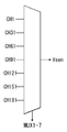
각각의 터치 센서(TC)에는 복수의 픽셀(P)들이 커플링된다. 도 3은 3x3 행렬 방식으로 나열된 9개의 픽셀(P)들이 하나의 터치 센서(TC)에 배정된 경우를 도시하고 있다. 공통전극(7)은 터치 센서(TC) 단위로 분할되고, 결국 공통전극(7)이 차지하는 면적이 터치 센서(TC)로 지칭될 수 있다. 각 터치 센서들(TC)은 센싱 라인(CH)들이 하나씩 배정되어 연결된다. 예를 들어, 1행1열의 터치 센서(TC1)에는 1행 1열의 센싱 라인(CH1)이 연결되고, 1행 2열의 터치 센서(TC2)에는 1행 2열의 센싱 라인(CH2)이 연결된다. 제1 채널 그룹(CG1)은 제1 열(TC_C1)에 배열되는 터치 센서(TC1,TC11,TC21...TC201)들과 연결되는 센싱 라인(CH)들을 포함하고, 제10 채널 그룹(CG10)은 제10 열(TC_C10)에 배열되는 터치 센서(TC10,TC20,TC30...TC210)들과 연결되는 센싱라인(CH)들을 포함한다. A plurality of pixels P are coupled to each touch sensor TC. FIG. 3 shows a case where nine pixels P arranged in a 3x3 matrix are assigned to one touch sensor TC. The
공통전극(7)은 디스플레이 기간 동안 픽셀들의 기준 전압인 공통 전압(Vcom)을 공급받고, 터치 센싱 기간 동안 터치 구동신호를 공급받는다. 본 발명의 터치 구동신호는 표시패널(100)을 블록 단위로 터치 센싱하기 위한 터치블록 구동신호들을 포함한다. 그리고 각 터치블록 구동신호는 터치기간과 터치기간 이외의 기간 동안에는 전압의 스윙폭이 달라진다. 터치블록 구동신호에 대한 자세한 설명은 후술하기로 한다. The
본 발명의 실시 예에 의한 표시패널(100)은 픽셀 구동 기간(Td) 동안에 픽셀(P)들을 통해서 영상을 표시하고, 터치 센싱 기간(Tt) 동안에 터치 센서(TC)들을 구동하여 터치 입력 여부를 감지한다. The
터치 구동 기간(Tt)은 제1 내지 제7 터치기간(Tt1~Tt7)을 포함하고, 각각의 터치기간은 하나의 터치블록(BLOCK)을 구동한다. 예컨대, 제1 터치기간(Tt1)은 제1 터치블록(BOLCK1)에 포함된 터치 센서(TC1*2~TC30*2)들을 구동하고, 제7 터치기간(Tt7)은 제7 터치블록(BLOCK7)에 포함된 터치 센서(TC181*2~TC210*2)들을 구동한다. The touch driving period Tt includes first to seventh touch periods Tt1 to Tt7, and each touch period drives one touch block BLOCK. For example, the first touch period Tt1 drives the touch sensors TC1 * 2 through TC30 * 2 included in the first touch block BOLCK1, the seventh touch period Tt7 drives the seventh touch block BLOCK7, The touch sensors TC181 * 2 to TC210 *
호스트 시스템(105)은 텔레비젼 시스템, 셋톱박스, 네비게이션 시스템, DVD 플레이어, 블루레이 플레이어, 개인용 컴퓨터(PC), 홈 시어터 시스템, 폰 시스템(Phone system) 중 어느 하나로 구현될 수 있다. 호스트 시스템(105)은 스케일러(scaler)를 내장한 SoC(System on chip)를 포함하여 입력 영상의 디지털 비디오 데이터(RGB)를 표시패널(100)에 표시하기에 적합한 포맷으로 변환한다. 호스트 시스템(105)은 디지털 비디오 데이터와 함께 타이밍 신호들(Vsync, Hsync, DE, MCLK)을 타이밍 콘트롤러(110)로 전송한다. 또한, 호스트 시스템(105)은 MCU(400)로부터 터치 데이터의 좌표 정보(Txy)를 입력받고, 이와 연계된 응용 프로그램을 실행한다.The
타이밍 콘트롤러(110)는 호스트 시스템(105)으로부터 입력되는 수직 동기신호(Vsync), 수평 동기신호(Hsync), 데이터 인에이블 신호(Data Enable, DE), 메인 클럭(MCLK) 등의 타이밍신호를 입력받아 데이터 구동부(120)와 게이트 구동부(130)의 동작 타이밍을 동기시킨다. 또한 타이밍 콘트롤러(110)는 게이트 타이밍 제어신호 및 데이터 타이밍 제어신호를 출력한다. 게이트 타이밍 제어신호는 게이트 스타트 펄스(Gate Start Pulse, GSP), 게이트 쉬프트 클럭(Gate Shift Clock), 게이트 출력 인에이블신호(Gate Output Enable, GOE) 등을 포함한다. 데이터 타이밍 제어신호는 소스 샘플링 클럭(Source Sampling Clock, SSC) 및 소스 출력 인에이블신호(Source Output Enable, SOE) 등을 포함한다.The
데이터 구동부(120)는 타이밍 콘트롤러로부터 영상 데이터(RGB)를 입력받아 정극성/부극성 감마보상전압으로 변환하여 정극성/부극성 데이터전압을 출력한다. 데이터 전압은 데이터 라인들(DL1~DLm)에 공급된다. The
게이트 구동부(130)는 타이밍 콘트롤러의 제어 하에 게이트 라인들(GL1~GLn)에 게이트 펄스를 순차적으로 공급한다. 게이트 구동부로부터 출력된 게이트 펄스는 데이터 전압에 동기된다. 게이트 구동부는 GIP(Gate in panel) 공정으로 픽셀 어레이와 함께 표시패널(100)의 하부 기판 상에 형성될 수도 있다. The
터치 구동회로부(200,300,400)는 센싱 라인(CH)들을 통해 터치 센서(TC)들에 교류 파형인 터치블록 구동신호를 공급하고, 센싱 라인(CH)들을 통해 감지된 터치 센서(TC)들의 전하 변화량을 바탕으로 터치 입력을 판단한다. 이를 위해서, 터치 구동회로부(200,300,400)는 터치 구동신호 생성부(200), 센싱 회로부(300) 및 MCU(400)를 포함한다.The touch
터치 구동신호 생성부(200)는 터치블록 구동신호를 생성하여 센싱 회로부(300)에 제공한다. The touch driving
도 5는 터치 구동신호 생성부의 구성을 나타내는 블록도이다. 도 6은 제1 구동신호 생성부, 제2 구동신호 생성부 및 제1 터치 구동신호 선택부의 실시 예를 나타내는 도면이다. 도 7은 터치 구동신호 생성부가 출력하는 터치블록 구동신호의 타이밍을 나타내는 도면이다. 5 is a block diagram showing a configuration of a touch driving signal generating unit. 6 is a diagram illustrating an embodiment of a first drive signal generator, a second drive signal generator, and a first touch drive signal selector. 7 is a timing chart of the touch block driving signal outputted from the touch driving signal generating unit.
도 5 내지 도 7을 참조하면, 터치 구동신호 생성부(200)는 제1 구동신호 생성부(211), 제2 구동신호 생성부(212)와 제1 내지 제7 터치 구동신호 선택부(221~227)를 포함한다.5 to 7, the touch driving
제1 구동신호 생성부(211)의 입력단자는 제1 하이전압(VH1) 및 제1 로우전압(VL1)을 입력받고, 선택단자는 펄스폭 제어신호(PWM)를 입력받는다. 제1 구동신호 생성부(211)는 펄스폭 제어신호(PWM)가 하이레벨일 때에 제1 하이전압(VH1)을 출력하고, 펄스폭 제어신호(PWM)가 로우레벨일 때에 제1 로우전압(VL1)을 출력한다. 그 결과 제1 구동신호 생성부(211)는 펄스폭 제어신호(PWM)와 주기가 동일하고, 제1 하이전압(VH1)에서 제1 로우전압(VL1)까지 스윙하는 제1 구동신호(VCOM1)를 출력한다. An input terminal of the first
제1 하이전압(VH1) 및 제1 로우전압(VL1)은 터치 구동신호 생성부(200)에서 생성되거나, 별도의 전원공급부에서 생성될 수 있다. 펄스폭 제어신호(PWM)는 타이밍 콘트롤러(110)로부터 입력받는다.The first high voltage VH1 and the first low voltage VL1 may be generated in the touch driving
제2 구동신호 생성부(212)의 입력단자는 제2하이전압(VH2) 및 제2로우전압(VL2)을 입력받고, 선택단자는 펄스폭 제어신호(PWM)를 입력받는다. 제2 구동신호 생성부(212)는 펄스폭 제어신호(PWM)가 하이레벨일 때에 제2하이전압(VH2)을 출력하고, 펄스폭 제어신호(PWM)가 로우레벨일 때에 제2로우전압(VL2)을 출력한다. 그 결과 제2 구동신호 생성부(212)는 펄스폭 제어신호(PWM)와 주기가 동일하고, 제2하이전압(VH2)에서 제2로우전압(VL2)까지 스윙하는 제2 구동신호(VCOM2)를 출력한다. 제2하이전압(VH2)은 제1 하이전압(VH1) 보다 낮은 전압레벨이고, 제2로우전압(VL2)은 제1 로우전압(VL1) 보다 높은 전압레벨이다. An input terminal of the second
제2하이전압(VH2) 및 제2로우전압(VL2)은 터치 구동신호 생성부(200)에서 생성되거나, 별도의 전원공급부에서 생성될 수 있다. The second high voltage VH2 and the second low voltage VL2 may be generated in the touch driving
제1 터치 구동신호 선택부(221)의 입력단자는 제1 구동신호(VCOM1) 및 제2 구동신호(VCOM2)를 입력받고, 선택단자는 제1 먹스 제어신호(MUX1)를 입력받는다. 제1 터치 구동신호 선택부(221)는 제1 먹스 제어신호(MUX1)가 하이레벨일 때에 제1 구동신호(VCOM1)를 출력하고, 제1 먹스 제어신호(MUX1)가 로우레벨일 때에 제2 구동신호(VCOM2)를 출력한다. 그 결과, 제1 터치 구동신호 선택부(221)가 출력하는 제1 터치블록 구동신호(VCOM_B1)는 제1 먹스 제어신호(MUX1)가 하이레벨인 동안 제1 하이전압(VH1)에서 제1 로우전압(VL1)까지 스윙하고, 제1 먹스 제어신호(MUX1)가 로우레벨인 동안 제2하이전압(VH2)에서 제2로우전압(VL2)까지 스윙한다.An input terminal of the first touch driving
이러한 방식으로, 제2 터치 구동신호 선택부(222)가 출력하는 제2 터치블록 구동신호(VCOM_B2)는 제2 먹스 제어신호(MUX2)가 하이레벨인 동안 제1 하이전압(VH1)에서 제1 로우전압(VL1)까지 스윙하고, 제2 먹스 제어신호(MUX2)가 로우레벨인 동안 제2하이전압(VH2)에서 제2로우전압(VL2)까지 스윙한다.In this manner, the second touch block driving signal VCOM_B2 output from the second touch driving
마찬가지로 제7 터치 구동신호 선택부(227)가 출력하는 제7 터치블록 구동신호(VCOM_B7)는 제7 먹스 제어신호(MUX7)가 하이레벨인 동안 제1 하이전압(VH1)에서 제1 로우전압(VL1)까지 스윙하고, 제7 먹스 제어신호(MUX7)가 로우레벨인 동안 제2하이전압(VH2)에서 제2로우전압(VL2)까지 스윙한다.Similarly, the seventh touch block driving signal VCOM_B7 outputted from the seventh touch driving
센싱 회로부(300)는 터치블록 구동신호(VCOM_B)를 이용하여 터치 센서(TC)를 구동한다. 센싱 회로부(300)는 터치 센서(TC)들의 정전 용량 변화량에 따라 가변하는 센싱 전압을 수신하고, 센싱 전압을 디지털 데이터인 터치 데이터(Tdata)로 변환하여 MCU(400)로 전송한다. 도 2에서와 같이 터치 센서(TC)들이 횡 방향으로 20개 배치되고, 열 방향으로 21개 배치된 표시패널에서, 제1 센싱 회로부(301) 및 제2 센싱 회로부(302)를 이용하여 터치 센서(TC)들을 구동하는 예를 살펴보면 다음과 같다. The
도 8은 센싱 회로부의 구성을 나타내는 도면이다. 8 is a diagram showing a configuration of a sensing circuit section.
도 8을 참조하면, 센싱 회로부(300)는 제1 센싱 회로부(301) 및 제2 센싱 회로부(302)를 포함한다. 제1 센싱 회로부(301)는 제1 터치 그룹(TG1)에 속한 터치 센서(TC)들을 구동하고, 제2 센싱 회로부(302)는 제2 터치 그룹(TG2)에 속한 터치 센서(TC)들을 구동한다. 제1 및 제2 센싱 회로부(301,302)의 구성은 실질적으로 동일할 수 있으며, 이하 본 명세서는 제1 센싱 회로부(301)를 중심으로 설명하기로 한다.Referring to FIG. 8, the
제1 센싱 회로부(301)는 제1 내지 제30 채널 회로부(301#1, 301#2, 301#3...301#30), 채널 멀티플렉서(320) 및 아날로그-디지털 변환기(330)를 포함한다. 각각의 채널 회로부(301#1, 301#2, 301#3...301#30)는 동일한 구성으로 구현될 수 있고, 이하 채널 회로부의 위치 및 순서와 상관없는 구성에 대해서는 "#"을 생략한 도면부호를 표기하기로 한다.The first
각 채널 회로부(310)는 채널 멀티플렉서(311), 센싱 유닛(312), 적분기(313) 및 홀더(314)를 포함한다. Each
채널 멀티플렉서(311)는 7:1 멀티플렉서로 구현되고, 입력 채널은 제1 터치블록(BLOCK1) 내지 제7 터치블록(BLOCK7)에 각각 포함되는 7개의 터치 센서(TC)들고 연결된다. 채널 멀티플렉서(311)는 제1 터치블록(BLOCK1) 내지 제7 터치블록(BLOCK7) 내에서 동일한 행과 동일한 열에 배치된 터치 센서(TC)들과 연결될 수 있다. The
도 9는 제1 채널 멀티플렉서(311#1)의 실시 예를 나타내는 도면이고, [표 1]은 먹스 제어신호들(MUX1~MUX7)에 의해서 선택되는 센싱 라인(CH)들을 나타내는 표이다.9 is a view showing an embodiment of the
도 9 및 [표 1]을 참조하면, 실시 예에 의한 제1 채널 멀티플렉서(311#1)의 입력 단자들은 제1 센싱라인(CH1), 제31 센싱라인(CH31), 제61 센싱라인(CH61), 제91 센싱라인(CH91), 제151 센싱라인(CH151) 및 제181 센싱라인(CH181)과 연결된다. 그리고 제1 채널 멀티플렉서(311#1)의 입력 단자는 제1 내지 제7 먹스 제어신호들(MUX1~MUX7) 중 어느 하나를 입력받는다. Referring to FIG. 9 and Table 1, the input terminals of the
제1 채널 멀티플렉서(311#1)는 제1 먹스 제어신호(MUX1)에 응답하여 제1 센싱라인(CH1)의 센싱전압을 출력하고, 제2 먹스 제어신호(MUX2)에 응답하여 제31 센싱라인(CH31)의 센싱전압을 출력한다. 그리고, 제7 먹스 제어신호(MUX7)에 응답하여 제181 센싱라인(CH181)의 센싱전압을 출력한다. The
이러한 방식으로 제2 채널 회로부(311#2)의 채널 멀티플렉서(311#2)는 제1 먹스 제어신호(MUX1) 내지 제7 먹스 제어신호(MUX7)에 각각 응답하여, 제2 센싱라인(CH2), 제32 센싱라인(CH32), 제62 센싱라인(CH62), 제92 센싱라인(CH92), 제122 센싱라인(CH122), 제152 센싱라인(CH152) 및 제182 센싱라인(CH182)의 센싱전압을 순차적으로 출력한다. In this manner, the
결과적으로 제1 센싱 회로부(301)의 제1 내지 제30 채널 회로부들(310#1~310#30)은 제1 먹스 제어신호(MUX1)에 응답하여, 제1 터치블록(BLCOK1)에 속하는 제1 내지 제30 터치센서들(TC1~TC30)의 센싱 전압을 획득한다. 이어서, 제1 내지 제30 채널 회로부들(310#1~310#30)은 제2 먹스 제어신호(MUX2)에 응답하여 제2 터치블록(BLOCK2)에 속하는 터치센서들(TC31~TC60)의 센싱전압을 획득하고, 제3 먹스 제어신호(MUC3)에 응답하여 제3 터치블록(BLCOK3)에 속하는 터치센서들(TC61~TC90)의 센싱전압을 획득한다. 그리고 제4 먹스 제어신호(MUX4) 내지 제7 먹스 제어신호(MUX7)에 각각 응답하여, 제4 터치블록(BLOCK4)에 속하는 터치센서들(TC91~TC120)의 센싱전압 내지 제7 터치블록(BLCO7)에 속하는 터치센서들(TC181~TC210)의 센싱전압을 순차적으로 획득한다. As a result, the first to thirtieth
터치블록들(BLOCK)은 센싱 회로부(300)와 평행하게 배열되기 때문에, 동일한 터치블록(BLOCK)에 속한 터치 센서(TC)들과 센싱 회로부(300)를 연결하는 센싱 라인(CH)은 길이 편차가 작게 된다. 이처럼 본 발명의 실시 예는 횡 방향으로 터치블록(BLCOK)을 배열하고 터치블록(BLOCK) 단위로 터치 구동을 하기 때문에, 동일한 기간에서 획득하는 센싱 전압(Vsen)들은 센싱 라인(CH)의 길이 편차에 의한 딜레이가 거의 없게 된다. 즉, 본 발명은 터치 구동기간(Tt)에 RC 지연에 의해서 센싱 전압(Vsen) 편차가 발생하는 것을 개선할 수 있기 때문에 센싱 감도를 높일 수 있다. Since the touch blocks BLOCK are arranged in parallel with the
센싱 유닛(312)은 채널 먹스부(311)를 경유하여 입력되는 센싱 전압을 수신하고, 수신된 센싱 전압을 증폭하여 출력한다. The
도 10은 센싱 유닛(312)을 나타내는 도면이다. Fig. 10 is a diagram showing the
도 10을 참조하면, 센싱 유닛(312)은 센싱라인(CH)으로부터 센싱 전압(Vsen)을 입력받는 반전 입력 단자(-)와, 터치블록 구동신호(VCOM_B)를 입력받는 비반전 입력 단자(+) 및 반전 입력 단자(-)와 출력단(Vout) 사이에 접속되는 피드백 커패시터(Cf)를 포함한다. 피드백 커패시터(Cf)는 반전 입력 단자(-)을 통해서 입력받는 센싱 전압을 적분한다. 리셋 스위치(RST)는 일정 주기로 턴-온되어서 피드백 커패시터(Cf)에 축전된 전하량을 리셋시킨다. 10, the
교류 파형의 터치블록 구동신호(VCOM_B)들이 센싱 유닛(312)에 공급되는 동안에, 데이터라인(DL)들과 게이트라인(GL)들에는 도 11에 도시된 것과 같이, 터치블록 구동신호(VCOM_B)와 동일한 위상의 교류신호(Vac)가 공급된다. 표시패널(100)의 데이터라인(DL)들 및 게이트라인(GL)들에 터치블록 구동신호(VCOM_B)와 동일한 위상의 교류신호(Vac)를 인가하면, 기생 용량 양단의 전압 차이가 줄어든다. 그 결과 표시패널(100)에 발생하는 기생 용량의 전하량을 줄일 수 있다. 즉, 터치블록 구동신호(VCOM_B1)와 표시패널(100)의 데이터라인(DL)들 및 게이트라인(GL)들에 동일한 위상의 교류신호(Vac)를 인가하면 터치 센서(TC)들과 신호 배선들(GL,GL) 간의 기생 용량을 최소화 할 수 있어서 터치 센싱 감도를 높일 수 있다.The touch block driving signal VCOM_B is supplied to the data lines DL and the gate lines GL while the touch block driving signals VCOM_B of the AC waveform are supplied to the
특히, 제k(k는 7이하의 자연수) 터치블록 구동신호(VCOM_Bk)는 제k 터치기간 이외에 출력되는 교류신호의 스윙폭이 제k 터치기간(Ttk) 동안에 출력되는 교류신호의 스윙폭보다 작게 제어된다. 즉, 제k 터치블록 구동신호(VCOM_Bk)는 k 번째 터치블록(BLOCKk)을 구동하는 기간 동안에는 전압 스윙폭을 크게 하여 터치 센서(TC)들의 정전 용량 변화를 크게 할 수 있다. 결과적으로 제k 터치블록 구동신호(VCOM_Bk)는 k 터치기간 동안에 터치 센싱 감도를 높일 수 있다. Particularly, the k-th touch block drive signal VCOM_Bk (k is a natural number of 7 or less) is set such that the swing width of the AC signal output during the k-th touch period is smaller than the swing width of the AC signal output during the k- Respectively. That is, the k-th touch block driving signal VCOM_Bk can increase the voltage swing width during the driving period of the k-th touch block BLOCKk to increase the capacitance change of the touch sensors TC. As a result, the k-th touch block driving signal VCOM_Bk can increase the touch sensing sensitivity during the k-touch period.
이와 동시에 제k 터치블록 구동신호(VCOM_Bk)는 k 터치기간 이외에는 교류신호의 전압 스윙폭을 작게하여 소비전력을 줄일 수 있다.At the same time, the k-th touch block driving signal VCOM_Bk decreases the voltage swing width of the AC signal in the k-touch period, thereby reducing power consumption.
제k 터치블록 구동신호(VCOM_Bk)가 스윙할 때, 전압의 기울기가 바뀌는 변곡점에서는 (Electro Magnetic Interference;이하, EMI)가 발생한다. 이때, 제k 터치블록 구동신호(VCOM_Bk)에 의한 EMI는 전압의 스윙폭에 비례한다. 본 발명에 의한 제k 터치블록 구동신호(VCOM_Bk)는 k 터치기간 이외에는 전압 스윙폭이 k 터치기간에 비해서 작아지기 때문에, 모든 구간에서 큰 폭으로 스윙하는 터치블록 구동신에 비하여 EMI를 줄일 수 있다. When the k-th touch block driving signal VCOM_Bk swings, Electro Magnetic Interference (hereinafter referred to as EMI) occurs at the inflection point where the slope of the voltage changes. At this time, EMI caused by the kth touch block driving signal VCOM_Bk is proportional to the swing width of the voltage. Since the voltage swing width of the k-th touch block driving signal VCOM_Bk is smaller than the k-touch period except the k-touch period, the EMI can be reduced compared with the touch block driving signal swinging in a wide range .
채널 회로부(310)의 적분기(313)는 센싱 유닛(312)의 출력을 적분한다. The
홀더(314)는 적분기(313)가 출력하는 전압을 일정 시간 마다 샘플링하고, 샘플링 한 아날로그 전압을 출력한다. The
터치 멀티플렉서(320)는 제1 내지 제30 채널 회로부들(310#1~310#30)의 홀더들(314#1~314#30)이 출력하는 아날로그 전압을 입력받아서 순차적으로 출력한다. 이를 위해서 터치 멀티플렉서(320)는 제1 내지 제30 채널 회로부들(310#1~310#30)의 출력단에 각각 연결되는 입력 단자를 갖는 30:1 멀티플렉서로 구현될 수 있다. The
아날로그 디지털 변환기(330)는 터치 멀티플렉서(320)가 출력하는 아날로그 전압을 디지털 데이터 값으로 변환한 터치 데이터(Tdata)를 생성한다. The analog-to-
MCU(400)는 센싱 회로부(300)의 아날로그 디지털 변환기(330)가 출력하는 터치 데이터(Tdata)를 입력받아서, 미리 설정된 터치 인식 알고리즘을 실행한다. 터치 인식 알고리즘으로는 공지된 어떠한 알고리즘도 가능하다. 터치 인식 알고리즘은 센싱 회로부(300)로부터 입력된 터치 원시 데이터를 소정의 문턱값과 비교하고, 그 문턱값 이상의 터치 원시 데이터를 터치 입력 위치의 터치 센서들로부터 얻어진 터치 입력 데이터로 판단된다. 터치 인식 알고리즘은 문턱값 이상의 터치 입력 데이터들 각각에 식별 코드를 부여하고 터치 입력 위치들 각각의 좌표를 계산한다. MCU(400)는 터치 입력 데이터들 각각의 식별 코드와 터치 좌표 정보(Txy)를 호스트 시스템(105)으로 전송한다.The
이상 설명한 내용을 통해 당업자라면 본 발명의 기술 사상을 일탈하지 아니하는 범위 내에서 다양한 변경 및 수정이 가능함을 알 수 있을 것이다. 따라서, 본 발명은 상세한 설명에 기재된 내용으로 한정되는 것이 아니라 특허 청구 범위에 의해 정해져야만 할 것이다.It will be apparent to those skilled in the art that various modifications and variations can be made in the present invention without departing from the spirit or scope of the invention. Therefore, the present invention should not be limited to the details described in the detailed description, but should be defined by the claims.
5: 픽셀전극
7: 공통전극
TC: 터치 센서
CH: 센싱라인
105: 호스트
110: 타이밍 콘트롤러
120: 데이터 구동부
130: 게이트 구동부
200: 구동신호 생성부
300: 센싱 회로부
400: MCU5: pixel electrode 7: common electrode
TC: Touch sensor CH: Sensing line
105: Host 110: Timing controller
120: Data driver 130: Gate driver
200: drive signal generator 300: sensing circuit
400: MCU
Claims (9)
상기 픽셀 어레이의 픽셀들에 영상 데이터를 기입하는 표시패널 구동회로부; 및
상기 센싱 라인들을 통해 상기 터치 센서들에 교류 파형인 터치블록 구동신호를 공급하고, 상기 센싱 라인들을 통해 감지된 터치 센서들의 전하 변화량을 바탕으로 터치 입력을 판단하는 터치 구동회로부를 포함하고,
상기 터치 구동회로부는 매 프레임의 상기 터치 구동기간 동안에, 제1 내지 제k(k는 자연수) 터치블록 구동신호를 생성하여 제1 내지 제k 터치블록을 순차적으로 구동하되,
제k 터치기간 동안에 출력되는 상기 제k 터치블록 구동신호는 상기 제k 터치기간 이외에 출력되는 교류신호의 스윙폭이 상기 제k 터치기간 동안에 출력되는 교류신호의 스윙폭보다 작게 제어되는 터치 센서 내장형 표시장치.A display panel in which touch sensors arranged in a pixel array and sensing lines connected to the touch sensors are arranged and driven in a time division manner in a pixel driving period and a touch driving period;
A display panel driving circuit for writing image data to pixels of the pixel array; And
And a touch driving circuit for supplying a touch block driving signal having an AC waveform to the touch sensors through the sensing lines and determining a touch input based on the amount of charge change of the touch sensors sensed through the sensing lines,
The touch driving circuit unit sequentially generates the first through k-th touch block driving signals by generating first through k-th (k is a natural number) touch block driving signals during the touch driving period of each frame,
Wherein the k-th touch block driving signal outputted during the k-th touch period is a touch sensor built-in display in which the swing width of the AC signal output in the k-th touch period is controlled to be smaller than the swing width of the AC signal output during the k- Device.
상기 제k 터치블록 구동신호는
상기 제k 터치기간 이외에는 상기 제1 하이전압 보다 낮은 제2 하이전압에서 상기 제1 로우전압 보다 높은 제2 로우전압까지 스윙하는 터치 센서 내장형 표시장치.The method according to claim 1,
The k < th > touch block drive signal
And swings from a second high voltage lower than the first high voltage to a second low voltage higher than the first low voltage except for the k-th touch period.
상기 터치 구동회로부는 제1 내지 제k 터치블록 구동신호를 생성하는 터치 구동신호 생성부를 포함하되,
상기 터치 구동신호 생성부는
제1 하이전압에서 제1 로우전압까지 스윙하는 제1 터치 구동신호를 생성하는 제1 구동신호 생성부;
상기 제2 하이전압에서 상기 제2 로우전압까지 스윙하는 제2 터치 구동신호를 생성하는 제2 구동신호 생성부; 및
상기 제k 터치기간 동안에 입력받는 제k 먹스 제어신호에 응답하여 상기 제k 터치블록 구동신호를 출력하는 제k 터치 구동신호 선택부를 포함하는 터치 센서 내장형 표시장치.The method according to claim 1,
The touch driving circuit unit includes a touch driving signal generating unit for generating first to k-th touch block driving signals,
The touch driving signal generating unit
A first driving signal generator for generating a first touch driving signal swinging from a first high voltage to a first low voltage;
A second driving signal generator for generating a second touch driving signal swinging from the second high voltage to the second row voltage; And
And a kth touch driving signal selector for outputting the kth touch block driving signal in response to the kth mux control signal received during the kth touch period.
상기 구동신호 생성부는 제1 터치블록 구동신호 선택부 내지 상기 제k 터치블록 구동신호 선택부를 포함하고,
제1 터치블록 구동신호 선택부 내지 상기 제k 터치블록 구동신호 선택부들은 각각 순차적으로 인가되는 제1 내지 상기 제k 먹스 제어신호에 응답하여 제1 터치블록 구동신호 내지 상기 제k 터치블록 구동신호를 출력하는 터치 센서 내장형 표시장치.The method of claim 3,
Wherein the driving signal generating unit includes a first touch block driving signal selecting unit and a kth touch block driving signal selecting unit,
The k-th touch block driving signal selecting unit and the k-th touch block driving signal selecting unit select the first to k-th touch block driving signals to the k-th touch block driving signal selecting unit in response to sequentially- The display device including a touch sensor.
상기 터치 구동기간 동안에, 상기 표시패널에 배치되는 데이터라인 및 게이트라인들은 상기 터치블록 구동신호와 동일한 위상의 교류신호를 공급받는 터치 센서 내장형 표시장치.The method according to claim 1,
Wherein the data line and the gate lines disposed on the display panel are supplied with an AC signal having the same phase as the touch block driving signal during the touch driving period.
상기 센싱 회로부는
상기 센싱라인과 연결되는 반전 입력 단자, 상기 터치블록 구동신호를 입력받는 비반전 입력 단자, 및 센싱 전압을 출력하는 센싱 유닛을 포함하는 터치 센서 내장형 표시장치.The method according to claim 1,
The sensing circuit section
And a sensing unit for outputting a sensing voltage. The display device of claim 1, wherein the sensing unit comprises: a sensing unit for sensing the touch block; a non-inverting input terminal for receiving the touch block driving signal;
상기 센싱 회로부는
제1 터치블록 내지 상기 k 터치블록에 각각 포함되는 k개의 터치센서들과 연결되는 k:1의 채널 멀티플렉서를 더 포함하고,
상기 채널 멀티플렉서는
순차적으로 인가되는 제1 내지 제k 먹스 제어신호에 응답하여 상기 제1 터치블록 내지 상기 제k 터치블록에 각각 포함되는 상기 k개의 터치센서들의 센싱전압을 순차적으로 수신하는 터치 센서 내장형 표시장치.The method according to claim 1,
The sensing circuit section
Further comprising a k: 1 channel multiplexer coupled to k touch sensors included in the first touch block to the k touch block,
The channel multiplexer
And sequentially receives the sensing voltages of the k touch sensors included in the first to k-th touch blocks in response to sequentially applied first to k-th mux control signals.
상기 터치블록들은 각각 j(j는 자연수)개의 터치센서들을 포함하고,
상기 센싱 회로부는 상기 j개의 터치센서들의 센싱전압을 동시에 수신하기 위한 j개의 채널 회로부를 포함하는 터치 센서 내장형 표시장치.8. The method of claim 7,
The touch blocks include j (j is a natural number) touch sensors,
Wherein the sensing circuit unit includes j channel circuit units for simultaneously receiving sensing voltages of the j touch sensors.
각각의 상기 채널 회로부와 연결되는 상기 터치센서들은 표시패널에서 동일한 열에 배열되는 터치 센서 내장형 표시장치.9. The method of claim 8,
Wherein the touch sensors connected to the respective channel circuit portions are arranged in the same column in the display panel.
Priority Applications (1)
| Application Number | Priority Date | Filing Date | Title |
|---|---|---|---|
| KR1020160056628A KR102552963B1 (en) | 2016-05-09 | 2016-05-09 | Display Device Having Touch Sensor |
Applications Claiming Priority (1)
| Application Number | Priority Date | Filing Date | Title |
|---|---|---|---|
| KR1020160056628A KR102552963B1 (en) | 2016-05-09 | 2016-05-09 | Display Device Having Touch Sensor |
Publications (2)
| Publication Number | Publication Date |
|---|---|
| KR20170126560A true KR20170126560A (en) | 2017-11-20 |
| KR102552963B1 KR102552963B1 (en) | 2023-07-11 |
Family
ID=60809046
Family Applications (1)
| Application Number | Title | Priority Date | Filing Date |
|---|---|---|---|
| KR1020160056628A Active KR102552963B1 (en) | 2016-05-09 | 2016-05-09 | Display Device Having Touch Sensor |
Country Status (1)
| Country | Link |
|---|---|
| KR (1) | KR102552963B1 (en) |
Cited By (4)
| Publication number | Priority date | Publication date | Assignee | Title |
|---|---|---|---|---|
| KR20190141490A (en) * | 2018-06-14 | 2019-12-24 | 엘지디스플레이 주식회사 | Touch display device, touch sensing circuit, and driving method |
| KR20210086332A (en) * | 2019-12-31 | 2021-07-08 | 엘지디스플레이 주식회사 | Touch display apparatus |
| CN114706499A (en) * | 2022-02-28 | 2022-07-05 | 北京奕斯伟计算技术有限公司 | Touch circuit, touch display circuit, display panel and touch detection method |
| CN119718115A (en) * | 2025-02-28 | 2025-03-28 | 绵阳惠科光电科技有限公司 | Touch display panel and display device |
Citations (4)
| Publication number | Priority date | Publication date | Assignee | Title |
|---|---|---|---|---|
| KR20150034046A (en) * | 2013-09-25 | 2015-04-02 | 엘지디스플레이 주식회사 | Apparatus for driving touch screen |
| KR20150049040A (en) * | 2013-10-29 | 2015-05-08 | 엘지디스플레이 주식회사 | Display Device With Integrated Touch Panel And Method For Driving The Same |
| KR20150056365A (en) * | 2013-11-15 | 2015-05-26 | 엘지디스플레이 주식회사 | Touch screen driving apparatus and method |
| KR20150124507A (en) * | 2014-04-28 | 2015-11-06 | 엘지디스플레이 주식회사 | Touch sensing device and driving method thereof |
-
2016
- 2016-05-09 KR KR1020160056628A patent/KR102552963B1/en active Active
Patent Citations (4)
| Publication number | Priority date | Publication date | Assignee | Title |
|---|---|---|---|---|
| KR20150034046A (en) * | 2013-09-25 | 2015-04-02 | 엘지디스플레이 주식회사 | Apparatus for driving touch screen |
| KR20150049040A (en) * | 2013-10-29 | 2015-05-08 | 엘지디스플레이 주식회사 | Display Device With Integrated Touch Panel And Method For Driving The Same |
| KR20150056365A (en) * | 2013-11-15 | 2015-05-26 | 엘지디스플레이 주식회사 | Touch screen driving apparatus and method |
| KR20150124507A (en) * | 2014-04-28 | 2015-11-06 | 엘지디스플레이 주식회사 | Touch sensing device and driving method thereof |
Cited By (5)
| Publication number | Priority date | Publication date | Assignee | Title |
|---|---|---|---|---|
| KR20190141490A (en) * | 2018-06-14 | 2019-12-24 | 엘지디스플레이 주식회사 | Touch display device, touch sensing circuit, and driving method |
| KR20210086332A (en) * | 2019-12-31 | 2021-07-08 | 엘지디스플레이 주식회사 | Touch display apparatus |
| CN114706499A (en) * | 2022-02-28 | 2022-07-05 | 北京奕斯伟计算技术有限公司 | Touch circuit, touch display circuit, display panel and touch detection method |
| CN114706499B (en) * | 2022-02-28 | 2024-04-12 | 北京奕斯伟计算技术股份有限公司 | Touch control circuit, touch control display circuit, display panel and touch control detection method |
| CN119718115A (en) * | 2025-02-28 | 2025-03-28 | 绵阳惠科光电科技有限公司 | Touch display panel and display device |
Also Published As
| Publication number | Publication date |
|---|---|
| KR102552963B1 (en) | 2023-07-11 |
Similar Documents
| Publication | Publication Date | Title |
|---|---|---|
| US9891747B2 (en) | Multi-touch sensitive display device and method for assigning touch identification therein | |
| CN108255333B (en) | Touch sensing system and driving method thereof | |
| US9946403B2 (en) | Display device, method for driving the same, and driving circuit thereof | |
| CN106598320B (en) | Display device with touch sensor and driving method thereof | |
| US9865219B2 (en) | Liquid crystal display device with an integrated touch panel and method of driving the same | |
| KR101588983B1 (en) | Display device and driving device thereof | |
| KR102008512B1 (en) | Touch sensing system and compensation method of edge portion thereof | |
| TWI514218B (en) | Display device with integrated touch screen and method of driving the same | |
| US10002590B2 (en) | Display device for sensing gesture and method of driving the same | |
| US10860126B2 (en) | Display device with built-in touch sensors | |
| TW201423523A (en) | Display device with integrated touch screen and method of driving the same | |
| KR102378398B1 (en) | Display with touch screen and driving circuit | |
| KR20140076054A (en) | Display device having touch sensors and control method of gate driving circuit thereof | |
| KR101503106B1 (en) | Apparatus and method for driving touch screen | |
| KR102552963B1 (en) | Display Device Having Touch Sensor | |
| KR20220087753A (en) | Apparatus for Touch Display | |
| KR101667078B1 (en) | Touch sensing device, system and enhancement method of touch report rate thereof | |
| US12061759B2 (en) | Touch sensing device and touch display driving device for reducing electromagnetic interference | |
| KR101862398B1 (en) | Display having touch sensor | |
| US12067191B2 (en) | Touch sensing device and driving method thereof | |
| KR20190069041A (en) | Display device having touch sensor using the same and driving method thereof | |
| KR101992853B1 (en) | Touch sensing system | |
| KR102016572B1 (en) | Touch sensing system |
Legal Events
| Date | Code | Title | Description |
|---|---|---|---|
| PA0109 | Patent application |
Patent event code: PA01091R01D Comment text: Patent Application Patent event date: 20160509 |
|
| PG1501 | Laying open of application | ||
| A201 | Request for examination | ||
| PA0201 | Request for examination |
Patent event code: PA02012R01D Patent event date: 20210406 Comment text: Request for Examination of Application Patent event code: PA02011R01I Patent event date: 20160509 Comment text: Patent Application |
|
| PE0902 | Notice of grounds for rejection |
Comment text: Notification of reason for refusal Patent event date: 20220920 Patent event code: PE09021S01D |
|
| E701 | Decision to grant or registration of patent right | ||
| PE0701 | Decision of registration |
Patent event code: PE07011S01D Comment text: Decision to Grant Registration Patent event date: 20230419 |
|
| GRNT | Written decision to grant | ||
| PR0701 | Registration of establishment |
Comment text: Registration of Establishment Patent event date: 20230704 Patent event code: PR07011E01D |
|
| PR1002 | Payment of registration fee |
Payment date: 20230705 End annual number: 3 Start annual number: 1 |
|
| PG1601 | Publication of registration |