KR20170016591A - Transparent Electrode and Method for fabricating the Same - Google Patents
Transparent Electrode and Method for fabricating the Same Download PDFInfo
- Publication number
- KR20170016591A KR20170016591A KR1020150109865A KR20150109865A KR20170016591A KR 20170016591 A KR20170016591 A KR 20170016591A KR 1020150109865 A KR1020150109865 A KR 1020150109865A KR 20150109865 A KR20150109865 A KR 20150109865A KR 20170016591 A KR20170016591 A KR 20170016591A
- Authority
- KR
- South Korea
- Prior art keywords
- transparent conductor
- nanostructure
- transparent electrode
- transparent
- comparative example
- Prior art date
- Legal status (The legal status is an assumption and is not a legal conclusion. Google has not performed a legal analysis and makes no representation as to the accuracy of the status listed.)
- Ceased
Links
Images


Classifications
-
- H—ELECTRICITY
- H01—ELECTRIC ELEMENTS
- H01B—CABLES; CONDUCTORS; INSULATORS; SELECTION OF MATERIALS FOR THEIR CONDUCTIVE, INSULATING OR DIELECTRIC PROPERTIES
- H01B1/00—Conductors or conductive bodies characterised by the conductive materials; Selection of materials as conductors
- H01B1/02—Conductors or conductive bodies characterised by the conductive materials; Selection of materials as conductors mainly consisting of metals or alloys
-
- H—ELECTRICITY
- H01—ELECTRIC ELEMENTS
- H01B—CABLES; CONDUCTORS; INSULATORS; SELECTION OF MATERIALS FOR THEIR CONDUCTIVE, INSULATING OR DIELECTRIC PROPERTIES
- H01B1/00—Conductors or conductive bodies characterised by the conductive materials; Selection of materials as conductors
- H01B1/06—Conductors or conductive bodies characterised by the conductive materials; Selection of materials as conductors mainly consisting of other non-metallic substances
- H01B1/08—Conductors or conductive bodies characterised by the conductive materials; Selection of materials as conductors mainly consisting of other non-metallic substances oxides
-
- H—ELECTRICITY
- H01—ELECTRIC ELEMENTS
- H01B—CABLES; CONDUCTORS; INSULATORS; SELECTION OF MATERIALS FOR THEIR CONDUCTIVE, INSULATING OR DIELECTRIC PROPERTIES
- H01B13/00—Apparatus or processes specially adapted for manufacturing conductors or cables
-
- H—ELECTRICITY
- H01—ELECTRIC ELEMENTS
- H01B—CABLES; CONDUCTORS; INSULATORS; SELECTION OF MATERIALS FOR THEIR CONDUCTIVE, INSULATING OR DIELECTRIC PROPERTIES
- H01B13/00—Apparatus or processes specially adapted for manufacturing conductors or cables
- H01B13/0016—Apparatus or processes specially adapted for manufacturing conductors or cables for heat treatment
-
- H—ELECTRICITY
- H01—ELECTRIC ELEMENTS
- H01B—CABLES; CONDUCTORS; INSULATORS; SELECTION OF MATERIALS FOR THEIR CONDUCTIVE, INSULATING OR DIELECTRIC PROPERTIES
- H01B13/00—Apparatus or processes specially adapted for manufacturing conductors or cables
- H01B13/0026—Apparatus for manufacturing conducting or semi-conducting layers, e.g. deposition of metal
-
- H—ELECTRICITY
- H01—ELECTRIC ELEMENTS
- H01B—CABLES; CONDUCTORS; INSULATORS; SELECTION OF MATERIALS FOR THEIR CONDUCTIVE, INSULATING OR DIELECTRIC PROPERTIES
- H01B13/00—Apparatus or processes specially adapted for manufacturing conductors or cables
- H01B13/0033—Apparatus or processes specially adapted for manufacturing conductors or cables by electrostatic coating
-
- H—ELECTRICITY
- H01—ELECTRIC ELEMENTS
- H01B—CABLES; CONDUCTORS; INSULATORS; SELECTION OF MATERIALS FOR THEIR CONDUCTIVE, INSULATING OR DIELECTRIC PROPERTIES
- H01B5/00—Non-insulated conductors or conductive bodies characterised by their form
- H01B5/14—Non-insulated conductors or conductive bodies characterised by their form comprising conductive layers or films on insulating-supports
Landscapes
- Engineering & Computer Science (AREA)
- Manufacturing & Machinery (AREA)
- Non-Insulated Conductors (AREA)
- Physics & Mathematics (AREA)
- Thermal Sciences (AREA)
Abstract
투명 전극 및 그 제조방법을 제공한다. 상기 투명 전극은 하나의 물질로 형성되는 나노 구조체 및 상기 나노 구조체 상에 상기 나노 구조체의 형상을 유지시키도록 코팅되는 제1 투명 전도체를 포함하되, 상기 나노 구조체는 결정질이다.A transparent electrode and a manufacturing method thereof are provided. The transparent electrode includes a nanostructure formed of one material and a first transparent conductor coated on the nanostructure to maintain the shape of the nanostructure, wherein the nanostructure is crystalline.
Description
본 발명은 투명 전극 및 그 제조방법에 관한 것으로, 보다 구체적으로는 열 안정성과 유연성 및 광 포집력이 우수한 투명 전극 및 그 제조방법에 관한 것이다.More particularly, the present invention relates to a transparent electrode having excellent thermal stability, flexibility, and light collecting ability, and a method of manufacturing the transparent electrode.
투명 전도성 전극(TCEs; Transparent Conductive Electrodes)의 중요성은 터치 패널, 평판 디스플레이, 다른 광전자 소자 등의 응용을 위해 그 중요성이 날로 커져가고 있다. TCO(Transparent conductor oxide)는 유기 태양전지 등의 분야에서 현재 투명 전극으로 가장 폭넓게 사용되는 재료이지만 단독으로 사용하는 경우에는 소성 재료이므로 공정 온도가 높고 외부의 물리적인 자극에 의하여 깨지기 쉬우며 휨 변형 등에 취약하다. 또한 폴리머 기판 위에 코팅했을 때 기판을 구부리면 막이 부서지는 단점 이 있다. The importance of Transparent Conductive Electrodes (TCEs) is becoming increasingly important for applications such as touch panels, flat panel displays, and other optoelectronic devices. Transparent conductor oxide (TCO) is the most widely used transparent electrode in the field of organic solar cell. However, when used alone, it is a fired material, so it has high process temperature and is easily broken by external physical stimulus. weak. Also, when the substrate is coated on the polymer substrate, the film is broken when the substrate is bent.
최근 이러한 TCO의 문제점들을 해결하기 위한 방안으로 플렉서블 투명 전극이면서 TCO를 대체 할 수 있는 재로 주목 받고 있는 것에 전도성 고분자, 탄소 나노 튜브, 그래핀, 그리고 금속 나노와이어 및 나노 입자가 있다. 그러나 탄소 나노 튜브 또는 그래핀은 전도도가 낮고 투과도 향상이 어렵다.Recently, conductive polymers, carbon nanotubes, graphenes, and metal nanowires and nanoparticles have been attracting attention as a flexible transparent electrode and a substitute for TCO as a solution for solving such TCO problems. However, carbon nanotubes or graphenes have low conductivity and difficult to improve the permeability.
본 발명이 해결하고자 하는 과제는 상기와 같은 문제점들을 극복하고 유연성이 개선된 투명 전극을 제공하는 것이다.SUMMARY OF THE INVENTION The present invention has been made to solve the above-mentioned problems, and it is an object of the present invention to provide a transparent electrode having improved flexibility.
본 발명이 해결하고자 하는 다른 과제는, 상기와 같은 문제점들을 극복하고 유연성이 개선된 투명 전극 제조 방법을 제공하는 것이다.Another problem to be solved by the present invention is to provide a transparent electrode manufacturing method which overcomes the above problems and has improved flexibility.
본 발명이 해결하고자 하는 과제들은 이상에서 언급한 과제들로 제한되지 않으며, 언급되지 않은 또 다른 과제들은 아래의 기재로부터 당업자에게 명확하게 이해될 수 있을 것이다.The problems to be solved by the present invention are not limited to the above-mentioned problems, and other matters not mentioned can be clearly understood by those skilled in the art from the following description.
상기 과제를 해결하기 위한 본 발명의 일 실시예에 따른 투명 전극은 하나의 물질로 형성되는 나노 구조체 및 상기 나노 구조체 상에 상기 나노 구조체의 형상을 유지시키도록 코팅되는 제1 투명 전도체를 포함하되,상기 나노 구조체는 결정질(Crystalline)다.According to an aspect of the present invention, there is provided a transparent electrode comprising: a nanostructure formed of a single material; and a first transparent conductor coated on the nanostructure to maintain the shape of the nanostructure, The nanostructure is crystalline.
상기 다른 과제를 해결하기 위한 본 발명의 일 실시예에 따른 투명 전극 제조 방법은 하나의 물질로 형성되는 나노 구조체를 형성하고, 상기 나노 구조체 상에 제1 투명 전도체를 형성하여 상기 나노 구조체를 코팅하는 것을 포함하되, 상기 제1 투명 전도체는 결정질이다.According to another aspect of the present invention, there is provided a method of fabricating a transparent electrode, comprising: forming a nanostructure formed of a single material; forming a first transparent conductor on the nanostructure to coat the nanostructure; Wherein the first transparent conductor is crystalline.
기타 실시예들의 구체적인 사항들은 상세한 설명 및 도면들에 포함되어 있다.The details of other embodiments are included in the detailed description and drawings.
본 발명의 일 실시예에 의하면 적어도 다음과 같은 효과가 있다.According to one embodiment of the present invention, at least the following effects are obtained.
즉, 본 발명의 일 실시예에 따른 투명 전극은 유연성이 개선되고 빛에 대한 표면적이 넓어 광 포집력을 향상시킬 수 있다. That is, the transparent electrode according to an exemplary embodiment of the present invention can improve the flexibility and improve the light collecting ability by enlarging the surface area of light.
또한, 본 발명의 일 실시예에 따른 투명 전극은 열 안정성이 개선되어 높은 온도에서의 가공도 가능할 수 있다.In addition, the transparent electrode according to an exemplary embodiment of the present invention has improved thermal stability and can be processed at a high temperature.
본 발명에 따른 효과는 이상에서 예시된 내용에 의해 제한되지 않으며, 더욱 다양한 효과들이 본 명세서 내에 포함되어 있다.The effects according to the present invention are not limited by the contents exemplified above, and more various effects are included in the specification.
도 1은 본 발명의 일 실시예에 따른 투명 전극의 구조를 설명하기 위한 부분 분해 사시도이다.
도 2는 도 1의 A-A를 따라 절단한 단면도이다.
도 3은 본 발명의 다른 실시예에 따른 투명 전극의 구조를 설명하기 위한 부분 분해 사시도이다.
도 4는 도 3의 B-B를 따라 절단한 단면도이다.
도 5는 비교예 1의 투명 전극의 구조를 설명하기 위한 사시도이다.
도 6은 비교예 2의 투명 전극의 구조를 설명하기 위한 부분 분해 사시도이다.
도 7은 도 3의 투명 전극, 비교예 1 및 2의 투명 전극의 파장에 따른 투과도를 설명하기 위한 그래프이다.
도 8은 본 발명의 일 실시예에 따른 투명 전극 제조 방법의 열처리 공정을 설명하기 위한 도면이다.
도 9는 비교예 2의 투명 전극의 열처리 후의 나노 와이어를 설명하기 위한 평면도이다.
도 10은 도 3의 투명 전극의 열처리 후의 나노 와이어를 설명하기 위한 평면도이다.
도 11은 도 3의 투명 전극과 비교예 2의 투명 전극의 전압 전류 특성을 설명하기 위한 그래프이다.
도 12는 도 3의 투명 전극과 비교예 2의 투명 전극의 반사도를 설명하기 위한 그래프이다.
도 13은 도 3의 투명 전극과 비교예 2의 투명 전극의 외부양자효율(EQE)을 설명하기 위한 그래프이다.
도 14는 도 3의 투명 전극과 비교예 2의 투명 전극의 내부양자효율(IQE)을 설명하기 위한 그래프이다.
도 15는 도 3의 투명 전극과 비교예 2의 투명 전극의 600nm 파장의 빛에서의 광반응을 설명하기 위한 그래프이다.
도 16은 도 3의 투명 전극과 비교예 2의 투명 전극의 900nm 파장의 빛에서의 광반응을 설명하기 위한 그래프이다.
도 17은 도 3의 투명 전극과 비교예 2의 투명 전극의 외부양자효율(EQE)의 파장 구간을 설명하기 위한 그래프이다.
도 18은 비교예 1의 투명 전극과 비교예 2의 투명 전극의 900nm 파장의 빛에서의 광반응을 설명하기 위한 그래프이다.
도 19 내지 도 22는 본 발명의 일 실시예에 따른 투명 전극 제조 방법을 설명하기 위한 중간 단계 도면들이다.
도 23은 온도에 따른 투명 전도체의 저항을 설명하기 위한 그래프이다.
도 24는 온도에 따른 투명 전도체의 투과도를 설명하기 위한 그래프이다.1 is a partially exploded perspective view illustrating a structure of a transparent electrode according to an embodiment of the present invention.
Fig. 2 is a cross-sectional view taken along AA of Fig.
3 is a partially exploded perspective view illustrating a structure of a transparent electrode according to another embodiment of the present invention.
4 is a cross-sectional view taken along line BB in Fig.
5 is a perspective view for explaining the structure of the transparent electrode of Comparative Example 1. Fig.
6 is a partially exploded perspective view for explaining the structure of the transparent electrode of Comparative Example 2. Fig.
FIG. 7 is a graph for illustrating transmittances according to wavelengths of the transparent electrode of FIG. 3 and the transparent electrodes of Comparative Examples 1 and 2. FIG.
8 is a view for explaining a heat treatment process of the transparent electrode manufacturing method according to an embodiment of the present invention.
9 is a plan view for explaining a nanowire after heat treatment of the transparent electrode of Comparative Example 2. Fig.
FIG. 10 is a plan view for explaining the nanowire after the heat treatment of the transparent electrode of FIG. 3; FIG.
11 is a graph for explaining voltage-current characteristics of the transparent electrode of FIG. 3 and the transparent electrode of Comparative Example 2. FIG.
12 is a graph for explaining the reflectivity of the transparent electrode of FIG. 3 and the transparent electrode of Comparative Example 2. FIG.
FIG. 13 is a graph for explaining the external quantum efficiency (EQE) of the transparent electrode of FIG. 3 and the transparent electrode of Comparative Example 2. FIG.
FIG. 14 is a graph for explaining the internal quantum efficiency (IQE) of the transparent electrode of FIG. 3 and the transparent electrode of Comparative Example 2. FIG.
FIG. 15 is a graph for explaining light reaction in the light of 600 nm wavelength of the transparent electrode of FIG. 3 and the transparent electrode of Comparative Example 2. FIG.
FIG. 16 is a graph for explaining light reaction in the light of 900 nm wavelength of the transparent electrode of FIG. 3 and the transparent electrode of Comparative Example 2. FIG.
FIG. 17 is a graph for explaining the wavelength interval of the external quantum efficiency (EQE) of the transparent electrode of FIG. 3 and the transparent electrode of Comparative Example 2. FIG.
18 is a graph for explaining the light reaction in the light of 900 nm wavelength of the transparent electrode of Comparative Example 1 and the transparent electrode of Comparative Example 2. Fig.
FIGS. 19 to 22 are intermediate steps for explaining a method of manufacturing a transparent electrode according to an embodiment of the present invention.
23 is a graph for explaining the resistance of the transparent conductor according to the temperature.
24 is a graph for explaining the transmittance of the transparent conductor according to the temperature.
본 발명의 이점 및 특징, 그리고 그것들을 달성하는 방법은 첨부되는 도면과 함께 상세하게 후술되어 있는 실시예들을 참조하면 명확해질 것이다. 그러나 본 발명은 이하에서 개시되는 실시예들에 한정되는 것이 아니라 서로 다른 다양한 형태로 구현될 것이며, 단지 본 실시예들은 본 발명의 개시가 완전하도록 하며, 본 발명이 속하는 기술분야에서 통상의 지식을 가진 자에게 발명의 범주를 완전하게 알려주기 위해 제공되는 것이며, 본 발명은 청구항의 범주에 의해 정의될 뿐이다. 명세서 전체에 걸쳐 동일 참조 부호는 동일 구성 요소를 지칭한다.BRIEF DESCRIPTION OF THE DRAWINGS The advantages and features of the present invention, and the manner of achieving them, will be apparent from and elucidated with reference to the embodiments described hereinafter in conjunction with the accompanying drawings. The present invention may, however, be embodied in many different forms and should not be construed as being limited to the embodiments set forth herein. Rather, these embodiments are provided so that this disclosure will be thorough and complete, and will fully convey the scope of the invention to those skilled in the art. Is provided to fully convey the scope of the invention to those skilled in the art, and the invention is only defined by the scope of the claims. Like reference numerals refer to like elements throughout the specification.
비록 제1, 제2 등이 다양한 소자, 구성요소 및/또는 섹션들을 서술하기 위해서 사용되나, 이들 소자, 구성요소 및/또는 섹션들은 이들 용어에 의해 제한되지 않음은 물론이다. 이들 용어들은 단지 하나의 소자, 구성요소 또는 섹션들을 다른 소자, 구성요소 또는 섹션들과 구별하기 위하여 사용하는 것이다. 따라서, 이하에서 언급되는 제1 소자, 제1 구성요소 또는 제1 섹션은 본 발명의 기술적 사상 내에서 제2 소자, 제2 구성요소 또는 제2 섹션일 수도 있음은 물론이다.Although the first, second, etc. are used to describe various elements, components and / or sections, it is needless to say that these elements, components and / or sections are not limited by these terms. These terms are only used to distinguish one element, element or section from another element, element or section. Therefore, it goes without saying that the first element, the first element or the first section mentioned below may be the second element, the second element or the second section within the technical spirit of the present invention.
소자(elements) 또는 층이 다른 소자 또는 층의 "위(on)" 또는 "상(on)"으로 지칭되는 것은 다른 소자 또는 층의 바로 위뿐만 아니라 중간에 다른 층 또는 다른 소자를 개재한 경우를 모두 포함한다. 반면, 소자가 "직접 위(directly on)" 또는 "바로 위"로 지칭되는 것은 중간에 다른 소자 또는 층을 개재하지 않은 것을 나타낸다.It is to be understood that when an element or layer is referred to as being "on" or " on "of another element or layer, All included. On the other hand, a device being referred to as "directly on" or "directly above" indicates that no other device or layer is interposed in between.
공간적으로 상대적인 용어인 "아래(below)", "아래(beneath)", "하부(lower)", "위(above)", "상부(upper)" 등은 도면에 도시되어 있는 바와 같이 하나의 소자 또는 구성 요소들과 다른 소자 또는 구성 요소들과의 상관관계를 용이하게 기술하기 위해 사용될 수 있다. 공간적으로 상대적인 용어는 도면에 도시되어 있는 방향에 더하여 사용시 또는 동작시 소자의 서로 다른 방향을 포함하는 용어로 이해되어야 한다. 예를 들면, 도면에 도시되어 있는 소자를 뒤집을 경우, 다른 소자의 "아래(below 또는 beneath)"로 기술된 소자는 다른 소자의 "위(above)"에 놓여질 수 있다. 따라서, 예시적인 용어인 "아래"는 아래와 위의 방향을 모두 포함할 수 있다. 소자는 다른 방향으로도 배향될 수 있으며, 이 경우 공간적으로 상대적인 용어들은 배향에 따라 해석될 수 있다.The terms spatially relative, "below", "beneath", "lower", "above", "upper" May be used to readily describe a device or a relationship of components to other devices or components. Spatially relative terms should be understood to include, in addition to the orientation shown in the drawings, terms that include different orientations of the device during use or operation. For example, when inverting an element shown in the figure, an element described as " below or beneath "of another element may be placed" above "another element. Thus, the exemplary term "below" can include both downward and upward directions. The elements can also be oriented in different directions, in which case spatially relative terms can be interpreted according to orientation.
본 명세서에서 사용된 용어는 실시예들을 설명하기 위한 것이며 본 발명을 제한하고자 하는 것은 아니다. 본 명세서에서, 단수형은 문구에서 특별히 언급하지 않는 한 복수형도 포함한다. 명세서에서 사용되는 "포함한다(comprises)" 및/또는 "포함하는(comprising)"은 언급된 구성요소, 단계, 동작 및/또는 소자는 하나 이상의 다른 구성요소, 단계, 동작 및/또는 소자의 존재 또는 추가를 배제하지 않는다.The terminology used herein is for the purpose of illustrating embodiments and is not intended to be limiting of the present invention. In the present specification, the singular form includes plural forms unless otherwise specified in the specification. It is noted that the terms "comprises" and / or "comprising" used in the specification are intended to be inclusive in a manner similar to the components, steps, operations, and / Or additions.
다른 정의가 없다면, 본 명세서에서 사용되는 모든 용어(기술 및 과학적 용어를 포함)는 본 발명이 속하는 기술분야에서 통상의 지식을 가진 자에게 공통적으로 이해될 수 있는 의미로 사용될 수 있을 것이다. 또 일반적으로 사용되는 사전에 정의되어 있는 용어들은 명백하게 특별히 정의되어 있지 않는 한 이상적으로 또는 과도하게 해석되지 않는다. Unless defined otherwise, all terms (including technical and scientific terms) used herein may be used in a sense commonly understood by one of ordinary skill in the art to which this invention belongs. Also, commonly used predefined terms are not ideally or excessively interpreted unless explicitly defined otherwise.
이하, 도 1 및 도 2를 참조하여, 본 발명의 일 실시예에 따른 투명 전극을 설명한다.Hereinafter, a transparent electrode according to an embodiment of the present invention will be described with reference to FIGS. 1 and 2. FIG.
도 1은 본 발명의 일 실시예에 따른 투명 전극의 구조를 설명하기 위한 부분 분해 사시도이고, 도 2는 도 1의 A-A를 따라 절단한 단면도이다.FIG. 1 is a partially exploded perspective view illustrating a structure of a transparent electrode according to an embodiment of the present invention, and FIG. 2 is a cross-sectional view taken along line A-A of FIG.
도 1을 참고하면, 본 발명의 일 실시예에 따른 투명 전극은 기판(100), 나노 구조체(300), 제1 투명 전도체(400) 및 상부 전극(500)을 포함한다.Referring to FIG. 1, a transparent electrode according to an exemplary embodiment of the present invention includes a
구체적으로, 기판(100)은 유리 기판 또는 실리콘(Si) 기판, 게르마늄(Ge) 기판 등의 단일 반도체 기판일 수도 있고, 갈륨비소(GaAs)기판과 같이 화합물 반도체 기판일 수도 있다. 또는 기판(100)은 예를 들어 유연 기판(flexible substrates)일 수 있다. 단, 이에 제한되는 것은 아니다.Specifically, the
나노 구조체(300)는 기판(100) 상에 위치할 수 있다. 나노 구조체(300)는 나노 와이어(nano wire) 또는 나노 입자(nano particle)을 포함할 수 있다. 도 1의 나노 구조체(300)는 예시적으로 나노 와이어를 포함하는 것으로 도시하였다. 나노 구조체(300)는 하나의 물질로 형성될 수 있다. 나노 구조체(300)는 순수한 금속, 실리사이드(Silicide) 및 저마나이드(Germanide) 중 적어도 하나를 포함할 수 있다. 상기 금속은 예를 들어, Ag, Ni, Al, Cu 및 Au 중 적어도 하나일 수 있다. 단, 이에 제한되는 것은 아니다.The
나노 구조체(300)가 기판(100) 상에 위치함에 따라 빛에 대한 표면적이 넓어지고, 투명 전극의 유연성이 증가할 수 있다. 즉, 나노 구조체(300)의 표면은 일반적인 투명 전극의 표면보다 넓으므로 빛을 받아들이는 수용 면적이 상대적으로 증가하게 된다. 이에 따라 투명 전극의 광 포집력이 우수해진다.As the
또한, 나노 구조체(300)가 투명 전극에 포함됨에 따라서, 투명 전극의 유연성이 증가할 수 있다. 즉, 투명 전극에 가해지는 외력에 대해서 투명 전극이 파손되지 않고 버티는 정도가 증가할 수 있다. 따라서, 투명 전극의 내구성이 증가할 수 있다.In addition, as the
나노 구조체(300)는 기판(100)의 상면의 일부를 덮을 수 있다. 즉, 나노 구조체(300)는 입자 또는 와이어 구조이므로, 각각의 입자 또는 와이어 사이의 틈을 통해서 기판(100)의 상면이 노출될 수 있다. 따라서 나노 구조체(300)는 기판(100)의 상면을 전부 덮지는 못하므로, 기판(100)의 상면의 일부는 나노 구조체(300)와 오버랩되지 않을 수 있다. 나노 구조체(300)는 예를 들어, 기판(100)의 표면의 10 내지 70%를 덮을 수 있다. 나노 구조체(300)가 기판(100)의 표면을 너무 많이 덮으면 투과도가 낮아질 수 있고, 나노 구조체(300)가 기판(100)의 표면을 너무 조금 덮으면 투명 전극의 유연성 및 내구성이 약해질 수 있다.The
제1 투명 전도체(400)는 기판(100) 상에 형성될 수 있다. 제1 투명 전도체(400)는 투명한 도전체 물질로 형성될 수 있다. 제1 투명 전도체(400)는 예를 들어, ITO(Indium-tin-oxide), AZO(Aluminum-zinc-oxide), 산화주석(tin-oxide), 산화 인듐(In2O3), Pt, Au 또는 IZO(Indium-zinc-oxide) 중에서 적어도 하나를 포함할 수 있다.The first
제1 투명 전도체(400)는 결정질(Crystalline)일 수 있다. 제1 투명 전도체(400)는 200 내지 900℃ 의 온도에서 증착되거나 열처리될 수 있다. 이에 따라, 비정질(amorphous)에서 결정질로 결정화 될 수 있다. 결정질인 제1 투명 전도체(400)는 비정질의 상태에서보다 투과도가 높을 수 있다. The first
한편, 상기 제1 투명 전도체(400)의 높이(h1)는 특별히 한정되는 것은 아니지만, 예를 들어, 10 nm 내지 500 nm 범위일 수 있다. 제1 투명 전도체(400)의 높이(h1)가 10nm 미만인 경우 전기 전도성이 충분치 않고, 입사광에 대한 반사율 저감 효과가 줄어들 수 있어 바람직하지 않다. 또한, 제1 투명 전도체(400)의 높이(h1)가 500 nm 이상인 경우, 전기 전도도는 높아지지만, 광전반응에 의해 발생하는 전자의 포집 성능이 낮아져 광전 소자의 성능을 저하시킬 수 있다. 나아가, 제1 투명 전도체(400)가 너무 두꺼우면, 반사율의 저감 효과가 줄어들 수 있어 바람직하지 않다. Meanwhile, the height h1 of the first
기존의 소자의 경우, 같은 물질을 도핑하여 PN 또는 PIN접합을 사용하였으나, 본 발명의 투명 전극은 이종접합(heterojunction)을 사용할 수 있다. 광 다이오드의 제조시에 도핑 공정을 이용하는 경우, 캐리어의 재결합(recombination)에 의한 손실이 클 수 있다. 그러나, 도핑 공정이 없는 이종접합(heterojunction)의 경우에는 캐리어의 손실률을 줄일 수 있다. 더욱이, ITO 등의 투명 전도체는 전기 전도성이 우수하고, 빛의 투과성도 우수하므로 이종접합 소자로서 빈번하게 사용된다.In the case of a conventional device, a PN or PIN junction is used by doping the same material, but the transparent electrode of the present invention can use a heterojunction. In the case of using a doping process in manufacturing a photodiode, loss due to recombination of carriers may be large. However, in the case of a heterojunction without a doping process, the carrier loss rate can be reduced. Furthermore, since transparent conductors such as ITO have excellent electrical conductivity and excellent light transmittance, they are frequently used as heterojunction devices.
투명 전극의 기판(100)과, 나노 구조체(300) 및 제1 투명 전도체(400) 내에서 전자들이 비대칭적으로 존재한다. 열적 평형상태에서 제1 투명 전도체(400)와 기판(100)의 접합으로 이루어진 다이오드 영역 내에서는 캐리어의 농도 구배에 의한 확산으로 전하의 불균형이 생기고, 이로 인해 전기장(electric field)이 형성된다.Electrons are asymmetrically present in the
이에, 제1 투명 전도체(400)와 기판(100)의 접합으로 이루어진 다이오드 영역 내부로, 다이오드 영역을 이루는 물질의 전도대(conduction band)와 가전자대(valence band) 사이의 에너지 차이인 밴드갭 에너지(band gap energy)보다 큰 에너지를 갖는 빛이 조사되었을 경우, 빛 에너지를 받은 전자들은 가전자대에서 전도대로 여기(excite)되며, 전도대로 여기된 전자들은 자유롭게 이동할 수 있게 된다.In the diode region formed by joining the first
구체적으로, 제1 투명 전도체(400) 및 나노 구조체(300)는 빛을 투과할 수 있으므로, 반사되지 않은 빛은 기판(100)에 도달할 수 있다. 도달된 빛에 의해 여기된 전자들은 기판(100)에서 비저항의 차이에 의해 제1 투명 전도체(400)로 쉽게 이동할 수 있다.Specifically, since the first
예를 들어, 기판(100)의 재질이 p형 실리콘인 경우 그 비저항은 약 1 내지 10 Ωcm가 될 수 있다. 제1 투명 전도체(400)가 ITO재질인 경우, 상기 실리콘의 비저항보다 훨씬 작은 비저항을 가질 수 있다. For example, when the material of the
이에 따라, 상기 여기된 전자들은 저항이 작은 제1 투명 전도체(400)로 쉽게 이동할 수 있다. 따라서, 다수의 전자가 기판(100)에서 제1 투명 전도체(400)로 이동하게 된다.Accordingly, the excited electrons can easily move to the first
따라서, 상기 여기된 전자의 확산에 의해 다이오드 영역 내부에 전압차(potential difference)가 생기게 되며, 다이오드 영역 양측에 위치하는 상부 전극(500)을 외부 회로에 연결하여 기전력을 활용할 수 있다.Accordingly, a potential difference is generated in the diode region due to the diffusion of the excited electrons, and the electromotive force can be utilized by connecting the
상부 전극(500)은 제1 투명 전도체(400) 상에 형성될 수 있다. 상부 전극(500)은 제1 투명 전도체(400)와 전기적으로 접속될 수 있다. 상부 전극(500)은 도전성 물질로 형성될 수 있다. 예를 들어, 상부 전극(500)은 금속을 포함할 수 있다. 예를 들어, 상부 전극(500)은 Ag, Au, Pt, Al 또는 Cu일 수 있다. 단, 이에 제한되는 것은 아니다.The
도시되진 않았지만, 기판(100)의 타면에 하부 전극이 형성될 수 있다. 하부 전극은 도전성 물질로 형성될 수 있다. 바람직하게는 하부 전극은 금속일 수 있다. 예를 들어, 하부 전극은 Ag, Au, Pt, Al 또는 Cu일 수 있다. 단, 이에 제한되는 것은 아니다.Although not shown, a lower electrode may be formed on the other surface of the
도 2를 참고하면, 본 발명의 나노 구조체(300)는 제1 투명 전도체(400)에 의해서 완전히 코팅될 수 있다. 즉, 나노 구조체(300)의 표면은 기판(100)과 제1 투명 전도체(400)에 의해서 완전히 둘러싸일 수 있다. 이에 따라, 나노 구조체(300)는 그 형상이 훼손되지 않고 유지될 수 있다. 제1 투명 전도체(400)는 나노 구조체(300)의 상면뿐만 아니라 그 사이사이를 채울 수 있다. 즉, 나노 구조체(300)와 제1 투명 전도체(400)는 일체로 하나의 투명전극의 역할을 할 수 있다.Referring to FIG. 2, the
이하, 도 3 및 도 4를 참조하면, 본 발명의 다른 실시예에 따른 투명 전극을 설명한다. 상술한 도 1의 실시예와 중복되는 부분은 생략하거나 간략히 한다.3 and 4, a transparent electrode according to another embodiment of the present invention will be described. The parts overlapping with the embodiment of FIG. 1 described above are omitted or briefly described.
도 3은 본 발명의 다른 실시예에 따른 투명 전극의 구조를 설명하기 위한 부분 분해 사시도이고, 도 4는 도 3의 B-B를 따라 절단한 단면도이다.FIG. 3 is a partially exploded perspective view illustrating a structure of a transparent electrode according to another embodiment of the present invention, and FIG. 4 is a cross-sectional view taken along line B-B of FIG.
도 3을 참조하면, 본 발명의 다른 실시예에 따른 투명 전극은 제2 투명 전도체(200)를 더 포함한다.Referring to FIG. 3, the transparent electrode according to another embodiment of the present invention further includes a second
제2 투명 전도체(200)는 기판(100) 상에 형성될 수 있다. 제2 투명 전도체(200)는 기판(100) 상에 컨포말하게 형성될 수 있다. 제2 투명 전도체(200)는 투명한 도전체 물질로 형성될 수 있다. 제2 투명 전도체(200)는 예를 들어, ITO(Indium-tin-oxide), AZO(Aluminum-zinc-oxide), 산화주석(tin-oxide), 산화 인듐(In2O3), Pt, Au 또는 IZO(Indium-zinc-oxide) 중에서 적어도 하나를 포함할 수 있다.The second
한편, 상기 제2 투명 전도체(200)의 높이(h2)는 특별히 한정되는 것은 아니지만, 예를 들어, 10 nm 내지 500 nm 범위일 수 있다. 제2 투명 전도체(200)의 높이(h2)가 10nm 미만인 경우 전기 전도성이 충분치 않고, 입사광에 대한 반사율 저감 효과가 줄어들 수 있어 바람직하지 않다. 또한, 제2 투명 전도체(200)의 높이(h2)가 500 nm 이상인 경우, 전기 전도도는 높아지지만, 광전반응에 의해 발생하는 전자의 포집 성능이 낮아져 광전 소자의 성능을 저하시킬 수 있다. 나아가, 제2 투명 전도체(200)가 너무 두꺼우면, 반사율의 저감 효과가 줄어들 수 있어 바람직하지 않다.On the other hand, the height h2 of the second
제2 투명 전도체(200) 상에 나노 구조체(300)가 형성될 수 있다. 그 위에 제1 투명 전도체(400)가 형성될 수 있다. 이에 따라, 나노 구조체(300)는 제2 투명 전도체(200)와 제1 투명 전도체(400)의 사이에 위치할 수 있다. 나노 구조체(300)는 제2 투명 전도체(200)와 제1 투명 전도체(400)에 의해서 코팅될 수 있다. 나노 구조체(300)는 제2 투명 전도체(200)와 제1 투명 전도체(400)의 코팅에 의해서 그 형상이 유지될 수 있다.The
나노 구조체(300)는 제2 투명 전도체(200)의 상면의 일부를 덮을 수 있다. 나노 구조체(300)는 제2 투명 전도체(200)의 상면을 전부 덮지는 못하므로, 제2 투명 전도체(200)의 상면의 일부는 나노 구조체(300)와 오버랩되지 않을 수 있다. 즉 , 나노 구조체(300)는 입자 또는 와이어 구조이므로, 각각의 입자 또는 와이어 사이의 틈을 통해서 제2 투명 전도체(200)의 상면이 노출될 수 있다. 따라서 나노 구조체(300)는 예를 들어, 제2 투명 전도체(200)의 표면의 10 내지 70%를 덮을 수 있다. 나노 구조체(300)가 제2 투명 전도체(200)의 표면을 너무 많이 덮으면 투과도가 낮아질 수 있고, 나노 구조체(300)가 제2 투명 전도체(200)의 표면을 너무 조금 덮으면 투명 전극의 유연성 및 내구성이 약해질 수 있다.The
제2 투명 전도체(200)의 두께(h2)는 제1 투명 전도체(400)의 두께(h1)와 같을 수 있다. 이에 따라, 나노 구조체(300)는 제2 투명 전도체(200) 및 제1 투명 전도체(400)가 결합된 구조에서 수직적으로 중심부에 위치할 수 있다. 단, 이에 제한되는 것은 아니고, 제2 투명 전도체(200)의 두께(h2)와 제1 투명 전도체(400)의 두께(h1)는 서로 다를 수도 있다.The thickness h2 of the second
도 4를 참고하면, 본 발명의 나노 구조체(300)는 제1 투명 전도체(400) 및 제2 투명 전도체(200)에 의해서 완전히 코팅될 수 있다. 즉, 나노 구조체(300)의 표면은 제2 투명 전도체(200)와 제1 투명 전도체(400)에 의해서 완전히 둘러싸일 수 있다. 이에 따라, 나노 구조체(300)는 그 형상이 훼손되지 않고 유지될 수 있다. 제1 투명 전도체(400) 및 제2 투명 전도체(300)는 나노 구조체(300)의 상면뿐만 아니라 그 사이사이를 채울 수 있다. 즉, 나노 구조체(300)와 제1 투명 전도체(400) 및 제2 투명 전도체(200)는 일체로 하나의 투명전극의 역할을 할 수 있다.Referring to FIG. 4, the
제2 투명 전도체(200)는 제1 투명 전도체(400)와 결합될 수 있다. 즉, 제2 투명 전도체(200)의 상면과 제1 투명 전도체(400)의 하면이 결합할 수 있다. 단, 제2 투명 전도체(200)의 상면의 일부는 나노 구조체(300)에 의해서 커버되므로 나노 구조체(300)에 의해서 커버되지 않는 제2 투명 전도체(200)의 상면의 일부가 제1 투명 전도체(400)의 하면과 결합될 수 있다.The second
실시예Example 1 One
p형 실리콘 웨이퍼를 기판으로 사용하였다. 기판 상에 도 2에 도시되었듯이, ITO(Indium-tin-oxide)재질의 제2 투명 전도체(200)를 형성한다. 제2 투명 전도체(200)는 100nm의 두께로 형성되었다. 그 위에 은 나노 와이어를 배치하고, 다시 제1 투명 전도체(400)를 ITO 재질로 형성한다. 제1 투명 전도체(400)는 100nm의 두께로 형성되었다. 제1 투명 전도체(400) 상에 상부 전극(500)을 형성한다.A p-type silicon wafer was used as the substrate. A second
비교예Comparative Example 1 One
도 5는 비교예 1의 투명 전극의 구조를 설명하기 위한 사시도이다. 도 5를 참고하면, 제2 투명 전도체(200)와 나노 구조체(300)를 형성하지 않고, ITO 재질의 제1 투명 전도체(400)를 기판(100) 상에 바로 형성하였다. 제1 투명 전도체(400)는 200nm의 두께로 형성되어 실시예 1과 직접적인 비교가 가능하도록 하였다. 제1 투명 전도체(400) 상에 상부 전극(500)을 형성하였다.5 is a perspective view for explaining the structure of the transparent electrode of Comparative Example 1. Fig. Referring to FIG. 5, a first
비교예Comparative Example 2 2
도 6은 비교예 2의 투명 전극의 구조를 설명하기 위한 부분 분해 사시도이다. 도 6을 참고하면, 제2 투명 전도체(200) 및 제1 투명 전도체(400)를 형성하지 않고, 은 나노 와이어 재질의 나노 구조체(300)를 기판(100) 상에 바로 형성하였다. 나노 구조체(300) 상에 상부 전극(500)을 형성하였다.6 is a partially exploded perspective view for explaining the structure of the transparent electrode of Comparative Example 2. Fig. Referring to FIG. 6, a
실험예Experimental Example 1 One
상기 실시예 1 및 비교예 1 내지 2의 투명 전극의 투과율을 입사광의 파장에 따라 측정하였다. The transmittance of the transparent electrode of Example 1 and Comparative Examples 1 and 2 was measured according to the wavelength of incident light.
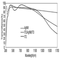
도 7은 도 3의 투명 전극, 비교예 1 및 2의 투명 전극의 파장에 따른 투과도를 설명하기 위한 그래프이다.FIG. 7 is a graph for illustrating transmittances according to wavelengths of the transparent electrode of FIG. 3 and the transparent electrodes of Comparative Examples 1 and 2. FIG.
도 7을 참고하면, ITO 층만을 단독으로 사용한 비교예 1과 ITO 층 대신에 은 나노 와이어를 사용한 비교예 2를 비교하면, 전반적으로 투과율이 높아지는 것을 확인할 수 있다. 즉, 일부 구간을 제외하고는 비교예 2의 투명 전극의 투과율이 높게 나타나고, 비교예 1의 투명 전극의 투과율이 더 높게 나타나는 구간에도 비교예 2의 투명 전극의 투과율이 크게 낮지 않은 것으로 확인된다. 즉, 투과율 부분에서는 은 나노 와이어를 사용한 비교예 2가 ITO 단독층을 사용한 비교예 1 보다 우수하다고 볼 수 있다.Referring to FIG. 7, it can be confirmed that the transmittance is generally increased as compared with Comparative Example 1 using only ITO layer alone and Comparative Example 2 using silver nanowire instead of ITO layer. That is, the transmittance of the transparent electrode of Comparative Example 2 is higher than that of Comparative Example 2, and the transmittance of the transparent electrode of Comparative Example 2 is not significantly lower in the region where the transmittance of the transparent electrode of Comparative Example 1 is higher. That is, in the transmittance portion, Comparative Example 2 using silver nanowire is superior to Comparative Example 1 using ITO single layer.
실시예 1의 투명 전극의 경우, 즉, ITO/은 나노 와이어/ITO의 이중 구조의 경우에 은 나노 와이어를 단독으로 사용한 비교예 2의 경우보다는 투과율이 낮아짐을 알 수 있다. 즉, 비교예 2의 투명 전극이 투과율의 특성에서는 가장 우수하다는 것을 알 수 있다. 다만, 실시예 1의 투명 전극은 비교예 1의 투명 전극에 비해서는 투과율이 전반적으로 우수하다는 것을 확인할 수 있다. 특히, 장파장 구간에서 비교예 1의 투명 전극은 투과율이 급격히 떨어짐에 반해 실시예 1의 투명 전극은 상대적으로 서서히 투과율이 내려가서 비교예 1의 투명 전극보다 우수함을 알 수 있다. 다른 구간은 실시예 1 및 비교예 1의 투명 전극이 서로 비슷한 정도의 높은 투과율을 보여줌을 확인할 수 있다.In the case of the transparent electrode of Example 1, that is, in the case of the double structure of ITO / silver nanowire / ITO, the transmittance is lower than that of Comparative Example 2 using silver nanowire alone. That is, it can be seen that the transparent electrode of Comparative Example 2 is the most excellent in the transmittance characteristics. However, it can be seen that the transparent electrode of Example 1 is superior to the transparent electrode of Comparative Example 1 in overall transmittance. In particular, in the long wavelength region, the transmittance of the transparent electrode of Comparative Example 1 dropped sharply, whereas the transmittance of the transparent electrode of Example 1 was relatively slower than that of the transparent electrode of Comparative Example 1. It can be confirmed that the transparent electrodes of Example 1 and Comparative Example 1 exhibit high transmissivity similar to each other in the other sections.
실시예 1의 투명 전극이 은 나노 와이어를 단독으로 사용한 비교예 2의 투명 전극보다 투과율에서는 앞서지 못하지만, 전기적 특성은 더 우수할 수 있다. 구체적으로, 실시예 1의 투명 전극의 시트 저항(sheet resistance)은 6.48Ω/□으로 측정되었다. 이에 반해, 비교예 1의 투명 전극의 단위 면적당 저항은 13.29Ω/□이고, 비교예 2의 투명 전극의 단위 면적당 저항은 28.63Ω/□이다.Although the transparent electrode of Example 1 is superior to the transparent electrode of Comparative Example 2 using silver nanowires alone, the electrical characteristics may be better, although the transmittance is not superior. Specifically, the sheet resistance of the transparent electrode of Example 1 was measured to be 6.48? / ?. On the contrary, the resistance per unit area of the transparent electrode of Comparative Example 1 was 13.29? /?, And the resistance per unit area of the transparent electrode of Comparative Example 2 was 28.63? / ?.
즉, ITO를 상하 방향으로 코팅한 은 나노 와이어를 사용한 실시예 1의 투명 전극이 전기적 특성에는 가장 우수할 수 있다. 따라서, 본 발명의 실시예 1이 투과율 측면에서도 나쁘지 않고, 전기적 특성에서도 월등하다는 것을 확인할 수 있다.That is, the transparent electrode of Example 1 using silver nanowires coated with ITO in the up and down direction can be most excellent in electrical characteristics. Therefore, it can be confirmed that Example 1 of the present invention is not inferior in terms of transmittance and superior in electrical properties.
실험예Experimental Example 2 2
실시예 1과 비교예 2의 열 안정성(thermal stability)를 비교하기 위해서 10분 동안 500℃의 온도에서 실시예 1과 비교예 2의 투명 전극에 열처리를 가했다. 열처리는 급속 열처리(Rapid Thermal processing, RTP)를 이용하였다. To compare the thermal stability of Example 1 and Comparative Example 2, the transparent electrodes of Example 1 and Comparative Example 2 were heat-treated at a temperature of 500 ° C for 10 minutes. Rapid thermal processing (RTP) was used for the heat treatment.
도 8은 본 발명의 일 실시예에 따른 투명 전극 제조 방법의 열처리 공정을 설명하기 위한 도면이고, 도 9는 비교예 2의 투명 전극의 열처리 후의 나노 와이어를 설명하기 위한 평면도이다. 도 10은 도 3의 투명 전극의 열처리 후의 나노 와이어를 설명하기 위한 평면도이다.FIG. 8 is a view for explaining a heat treatment process of a transparent electrode manufacturing method according to an embodiment of the present invention, and FIG. 9 is a plan view for explaining a nanowire after heat treatment of a transparent electrode of Comparative Example 2. FIG. FIG. 10 is a plan view for explaining the nanowire after the heat treatment of the transparent electrode of FIG. 3; FIG.
도 8을 참고하면, 시간에 따른 열처리의 온도를 확인할 수 있다. 300℃ 이하에서 2분간 300℃에 도달할 때까지 가열하고, 300℃에서 2분간 가열한 뒤 500℃까지 온도를 2분간 올리고, 10분간 500℃에서 열처리를 한다. 이러한 열처리는 ITO를 증착하고 경화시키는 공정에서 사용될 수 있다.Referring to FIG. 8, it is possible to confirm the temperature of the heat treatment with time. Heated at 300 ° C or lower for 2 minutes until reaching 300 ° C, heated at 300 ° C for 2 minutes, heated to 500 ° C for 2 minutes, and heat-treated at 500 ° C for 10 minutes. This heat treatment can be used in the process of depositing and curing ITO.
도 9를 참고하면, 비교예 2의 나노 와이어는 열처리에 의해 끊어짐을 확인할 수 있다. 일반적으로, 은 나노 와이어는 약 200℃의 온도에서 연결이 끊어질 수 있다. 따라서, 비교예 2의 나노 와이어도 열에 바로 노출되어 와이어의 연결이 끊어지고, 그 형상을 유지할 수 없다.Referring to FIG. 9, it can be confirmed that the nanowire of Comparative Example 2 is broken by heat treatment. Generally, silver nanowires can be disconnected at temperatures of about 200 < 0 > C. Therefore, the nanowire of Comparative Example 2 is also directly exposed to the heat, the connection of the wire is broken, and the shape can not be maintained.
이에 반해, 도 10을 참고하면, 실시예 1의 나노 와이어는 열처리 후에도 그 형상을 그대로 유지하고 끊어지지 않음을 알 수 있다. 즉, 실시예 1의 은 나노 와이어는 ITO에 의해서 코팅이 되어 200℃가 훨씬 넘는 500℃의 급속 열처리의 온도를 견딜 수 있다. 이에 따라, 상기 열처리는 투명 전극의 제조 공정에서 물질의 증착에 사용될 수 있으므로, 은 나노 와이어의 열 안정성에 따라 공정의 온도 조건의 제한이 결정될 수 있다. 따라서, 실시예 1의 투명 전극은 비교예 2에 비해서 우수한 열 안정성을 가질 수 있고, 제조 공정의 자유도도 높아질 수 있다.On the other hand, referring to FIG. 10, it can be seen that the nanowire of Example 1 retains its shape even after heat treatment and is not broken. That is, the silver nanowire of Example 1 is coated with ITO and can withstand the temperature of the rapid thermal annealing at a temperature of more than 200 ° C of 500 ° C. Accordingly, the heat treatment can be used for deposition of the material in the process of manufacturing the transparent electrode, so that the limitation of the temperature condition of the process can be determined according to the thermal stability of the silver nanowire. Therefore, the transparent electrode of Example 1 can have excellent thermal stability as compared with Comparative Example 2, and the degree of freedom of the manufacturing process can be increased.
실험예Experimental Example 3 3
상기 실시예 1 및 비교예 2의 전류 전압 특성, 반사도, 외부 양자 효율 및 내부 양자 효율을 측정하였다.The current voltage characteristics, reflectivity, external quantum efficiency and internal quantum efficiency of Example 1 and Comparative Example 2 were measured.
도 11은 도 3의 투명 전극과 비교예 2의 투명 전극의 전압 전류 특성을 설명하기 위한 그래프이고, 도 12는 도 3의 투명 전극과 비교예 2의 투명 전극의 반사도를 설명하기 위한 그래프이다. 도 11은 도 2의 투명 전극과 비교예 2의 투명 전극의 외부양자효율(external quantum efficiency, EQE)을 설명하기 위한 그래프이고, 도 14는 도 2의 투명 전극과 비교예 2의 투명 전극의 내부양자효율(internal quantum efficiency, IQE)을 설명하기 위한 그래프이다.FIG. 11 is a graph for explaining voltage-current characteristics of the transparent electrode of FIG. 3 and the transparent electrode of Comparative Example 2, and FIG. 12 is a graph for explaining the reflectivity of the transparent electrode of FIG. 3 and the transparent electrode of Comparative Example 2. FIG. 11 is a graph for explaining the external quantum efficiency (EQE) of the transparent electrode of FIG. 2 and the transparent electrode of Comparative Example 2, FIG. 14 is a graph for explaining the external quantum efficiency And is a graph for explaining quantum efficiency (IQE).
*도 11을 참조하면, 실시예 1의 ITO/AgNW(은 나노 와이어)/ITO/p-Si의 구조와 비교예 2의 AgNW/p-Si 구조의 I-V 곡선이 도시되어 있다. 실시예 1의 구조는 시트 저항이 낮으므로, V>0인 영역에서 기울기가 비교예 2의 투명 전극보다 상대적으로 높음을 알 수 있다.11, the structure of ITO / AgNW (silver nanowire) / ITO / p-Si of Example 1 and the I-V curve of AgNW / p-Si structure of Comparative Example 2 are shown. It can be seen that the structure of Example 1 has a relatively low sheet resistance, so that the slope in the region of V > 0 is relatively higher than that of the transparent electrode of Comparative Example 2. [
도 12를 참고하면, 실시예 1의 ITO/AgNW/ITO/p-Si의 구조와 비교예 2의 AgNW/p-Si 구조의 반사도 곡선이 도시되어 있다. 파장의 전 영역에 걸쳐서 실시예 1의 투명 전극의 반사도는 비교예 2의 반사도보다 낮음을 알 수 있다. 즉, 입사광의 반사도가 낮으므로 투명 전극의 효율은 상승할 수 있다.Referring to FIG. 12, the reflectance curves of the ITO / AgNW / ITO / p-Si structure of Example 1 and the AgNW / p-Si structure of Comparative Example 2 are shown. The reflectivity of the transparent electrode of Example 1 is lower than that of Comparative Example 2 over the entire wavelength range. That is, since the reflectivity of the incident light is low, the efficiency of the transparent electrode can be increased.
도 13을 참고하면, 실시예 1의 ITO/AgNW/ITO/p-Si의 구조와 비교예 2의 AgNW/p-Si 구조의 외부 양자 효율 곡선이 도시되어 있다. 반사도와 관련하여 실시예 1의 반사도가 낮으므로 실시예 1의 투명 전극의 외부 양자 효율이 비교예 2의 투명 전극의 외부 양자 효율 보다 높음을 알 수 있다. Referring to FIG. 13, the structure of ITO / AgNW / ITO / p-Si of Example 1 and the external quantum efficiency curve of AgNW / p-Si structure of Comparative Example 2 are shown. It can be seen that the external quantum efficiency of the transparent electrode of Example 1 is higher than the external quantum efficiency of the transparent electrode of Comparative Example 2 because the reflectivity of Example 1 is low with respect to the reflectivity.
도 14를 참고하면, 실시예 1의 ITO/AgNW/ITO/p-Si의 구조와 비교예 2의 AgNW/p-Si 구조의 내부 양자 효율 곡선이 도시되어 있다. 내부 양자 효율에 있어서는 미세하게 비교예 2의 투명 전극이 실시예 1의 투명 전극보다 높게 측정되었다.Referring to FIG. 14, the ITO / AgNW / ITO / p-Si structure of Example 1 and the internal quantum efficiency curve of the AgNW / p-Si structure of Comparative Example 2 are shown. In the internal quantum efficiency, the transparent electrode of Comparative Example 2 was measured to be slightly higher than that of the transparent electrode of Example 1.
즉, 도 11 내지 도 14의 그래프를 참조하면, 실시예 1의 투명 전극이 비교예 2의 투명 전극보다 상대적으로 반사도가 감소하여 투명 전극 외부에서 광자가 에너지로 변환되는 효율이 높음을 알 수 있다.In other words, referring to the graphs of FIGS. 11 to 14, it can be seen that the reflectivity of the transparent electrode of Example 1 is lower than that of the transparent electrode of Comparative Example 2, so that the efficiency of converting photons into energy outside the transparent electrode is high .
실험예Experimental Example 3 3
상기 실시예 1 및 비교예 2의 광 반응 특성(photoresponse)을 측정하였다.The photoresponse of Example 1 and Comparative Example 2 was measured.
도 15는 도 3의 투명 전극과 비교예 2의 투명 전극의 600nm 파장의 빛에서의 광반응을 설명하기 위한 그래프이고, 도 16은 도 3의 투명 전극과 비교예 2의 투명 전극의 900nm 파장의 빛에서의 광반응을 설명하기 위한 그래프이다. 도 17은 도 2의 투명 전극과 비교예 2의 투명 전극의 외부양자효율(EQE)의 파장 구간을 설명하기 위한 그래프이다.FIG. 15 is a graph for explaining light reaction in the light of 600 nm wavelength of the transparent electrode of FIG. 3 and the transparent electrode of Comparative Example 2, FIG. 16 is a graph illustrating the light response of the transparent electrode of FIG. This is a graph for explaining the light reaction in light. FIG. 17 is a graph for explaining the wavelength interval of the external quantum efficiency (EQE) of the transparent electrode of FIG. 2 and the transparent electrode of Comparative Example 2. FIG.
도 15를 참고하면, 파장이 600nm일 때, 실시예 1의 ITO/AgNW/ITO/p-Si의 구조와 비교예 2의 AgNW/p-Si 구조의 시간에 따른 전류 곡선이 도시되어 있다. 입사광의 600nm의 파장에서 광반응은 실시예 1의 투명 전극이 비교예 2의 투명 전극보다 높게 측정됨을 알 수 있다.Referring to FIG. 15, the current curve of ITO / AgNW / ITO / p-Si of Example 1 and the AgNW / p-Si structure of Comparative Example 2 over time are shown at a wavelength of 600 nm. It can be seen that the photoreaction at the wavelength of 600 nm of the incident light is higher than that of the transparent electrode of the comparative example 2.
도 16을 참고하면, 파장이 900nm일 때, 실시예 1의 ITO/AgNW/ITO/p-Si의 구조와 비교예 2의 AgNW/p-Si 구조의 시간에 따른 전류 곡선이 도시되어 있다. 입사광의 900nm의 파장에서 광반응은 실시예 1의 투명 전극이 비교예 2의 투명 전극보다 높게 측정됨을 알 수 있다. Referring to FIG. 16, the current curve of ITO / AgNW / ITO / p-Si of Example 1 and the AgNW / p-Si structure of Comparative Example 2 over time are shown at a wavelength of 900 nm. It can be seen that the photoreaction at the wavelength of 900 nm of the incident light is higher than that of the transparent electrode of Comparative Example 2.
도 17을 참고하면, 500 내지 1050nm 이상에서는 외부 양자 효율이 실시예 1의 투명 전극이 비교예 2의 투명 전극보다 높게 측정되었다. 이에 따라 도 15 및 도 16와 같이 파장이 600nm 및 900nm인 구간에서는 광반응이 실시예 1의 투명 전극이 비교예 2의 투명 전극보다 높게 나타날 수 있다.17, the external quantum efficiency of the transparent electrode of Example 1 was higher than that of the transparent electrode of Comparative Example 2 at 500 to 1050 nm or more. Accordingly, as shown in FIG. 15 and FIG. 16, the transparent electrode of Example 1 may exhibit a higher photoreaction than the transparent electrode of Comparative Example 2 in a region having a wavelength of 600 nm and 900 nm.
**
실험예Experimental Example 4 4
상기 비교예 1 및 비교예 2의 광 반응 특성을 측정하였다.The photoreaction characteristics of Comparative Example 1 and Comparative Example 2 were measured.
도 18은 비교예 1의 투명 전극과 비교예 2의 투명 전극의 900nm 파장의 빛에서의 광반응을 설명하기 위한 그래프이다.18 is a graph for explaining the light reaction in the light of 900 nm wavelength of the transparent electrode of Comparative Example 1 and the transparent electrode of Comparative Example 2. Fig.
도 18을 참고하면, 파장이 900nm일 때, 비교예 1의 ITO/p-Si의 구조와 비교예 2의 AgNW/p-Si 구조의 시간에 따른 전류 곡선이 도시되어 있다. 입사광의 900nm의 파장에서 광반응은 비교예 2의 투명 전극이 비교예 1의 투명 전극보다 훨씬 높게 측정됨을 알 수 있다.Referring to FIG. 18, the current curve of the ITO / p-Si structure of Comparative Example 1 and the AgNW / p-Si structure of Comparative Example 2 over time are shown at a wavelength of 900 nm. It can be seen that the photoreaction at the wavelength of 900 nm of the incident light is much higher than that of the transparent electrode of Comparative Example 1 in the transparent electrode of Comparative Example 2.
도 15 내지 도 18의 결과를 종합하면 실시예 1의 ITO/AgNW/ITO/p-Si 구조의 투명 전극의 광반응 특성이 비교예 2의 AgNW/p-Si 구조의 투명 전극의 광반응 특성보다 높고, 비교예 2의 투명 전극의 광반응 특성이 비교예 1의 ITO/p-Si 구조의 투명 전극의 광반응 특성보다 높다. 즉, 실시예 1의 투명 전극의 광반응 특성이 비교예 1의 투명 전극의 광반응 특성보다 높다.15 to 18, the photoreaction characteristics of the transparent electrode of the ITO / AgNW / ITO / p-Si structure of Example 1 were compared with those of the transparent electrode of the AgNW / p-Si structure of Comparative Example 2 And the photoreaction characteristics of the transparent electrode of Comparative Example 2 are higher than those of the transparent electrode of ITO / p-Si structure of Comparative Example 1. [ That is, the photoreaction characteristic of the transparent electrode of Example 1 is higher than that of the transparent electrode of Comparative Example 1. [
이하, 도 19 내지 도 22를 참조하여 본 발명의 일 실시예에 따른 투명 전극 제조 방법을 설명한다. 제조되는 투명 전극은 도 3의 투명 전극이다. 상술한 설명과 중복되는 부분은 간략히 하거나 생략한다.Hereinafter, a method of manufacturing a transparent electrode according to an embodiment of the present invention will be described with reference to FIGS. The transparent electrode to be manufactured is the transparent electrode shown in Fig. The portions overlapping with the above description will be simplified or omitted.
도 19 내지 도 22는 본 발명의 일 실시예에 따른 투명 전극 제조 방법을 설명하기 위한 중간 단계 도면들이다. FIGS. 19 to 22 are intermediate steps for explaining a method of manufacturing a transparent electrode according to an embodiment of the present invention.
도 19를 참고하면, 기판(100)을 제공한다.Referring to FIG. 19, a
기판(100)은 유리 기판, 실리콘(Si) 기판, 게르마늄(Ge) 기판 등의 단일 반도체 기판일 수도 있고, 갈륨비소(GaAs)기판과 같이 화합물 반도체 기판일 수도 있다.The
도 20을 참조하면, 기판(100) 상에 제2 투명 전도체(200)를 형성한다. 제2 투명 전도체(200)는 100 내지 900℃의 온도에서 증착될 수 있다. 단, 이에 제한되는 것은 아니다. 제2 투명 전도체(200)는 기판(100) 상에 컨포말하게 형성될 수 있다. Referring to FIG. 20, a second
이 때, 제2 투명 전도체(200)는 상온에서 증착될 수 있다. 상온에서 증착된 제2 투명 전도체(200)는 비정질일 수 있다. 추후에 제2 투명 전도체(200)는 200 내지 900℃의 온도에서 열처리될 수 있다. 단, 이에 제한되는 것은 아니다.At this time, the second
제2 투명 전도체(200)는 200 내지 900℃의 온도에서 증착될 수 있다. 이러한 경우에 제2 투명 전도체(200)는 결정질일 수 있다.The second
도 21을 참조하면, 제2 투명 전도체(200) 상에 나노 구조체(300)를 형성할 수 있다. 나노 구조체(300)는 나노 입자 또는 나노 와이어를 포함할 수 있다. 이 때, 나노 구조체(300)는 복합 구조가 아닌 하나의 물질로 형성될 수 있다. 나노 구조체(300)는 순수한 금속, 실리사이드(Silicide) 및 저마나이드(Germanide) 중 적어도 하나를 포함할 수 있다. 상기 금속은 예를 들어, Ag, Ni 및 Au 중 적어도 하나일 수 있다. 단, 이에 제한되는 것은 아니다.Referring to FIG. 21, the
도 22를 참조하면, 제2 투명 전도체(200) 및 나노 구조체(300) 상에 제1 투명 전도체(400)를 형성할 수 있다. 제1 투명 전도체(400) 및 제2 투명 전도체(200)는 나노 구조체(300)를 코팅하여 나노 구조체(300)의 형상이 유지되도록 할 수 있다. 이 때, 제1 투명 전도체(400)는 200 내지 900℃ 사이의 온도에서 결정질로 증착될 수 있다. 단, 이에 제한되는 것은 아니다.Referring to FIG. 22, a first
제1 투명 전도체(400)는 상온(room temperature)에서 형성되어 열처리 과정을 거칠 수 있다. 이 때는, 제2 투명 전도체(200)가 같이 상온에서 증착되어 같이 열처리 과정을 거칠 수 있다. 상기 열처리 과정은 200 내지 900℃ 사이의 온도에서 수행될 수 있다. 이 때, 제1 투명 전도체(400) 및 제2 투명 전도체(200)는 모두 비정질에서 결정질이 될 수 있다.The first
이 때, 제1 투명 전도체(400) 및 제2 투명 전도체(200)에 의해서 나노 구조체(300)는 연결이 끊어지지 않고 그대로의 형상을 유지할 수 있다. 이어서, 제1 투명 전도체(400) 상에 상부 전극(500)을 형성할 수 있다.At this time, the first
도 23은 온도에 따른 투명 전도체의 저항을 설명하기 위한 그래프이고, 도 24는 온도에 따른 투명 전도체의 투과도를 설명하기 위한 그래프이다.FIG. 23 is a graph for explaining the resistance of the transparent conductor according to the temperature, and FIG. 24 is a graph for explaining the transparency of the transparent conductor according to the temperature.
도 23을 참고하면, 증착 시 또는 열처리시의 온도가 가로축이고, 그에 따른 ITO 필름의 저항이 세로축이다. 즉, 증착 시 또는 열처리시의 온도가 높아질수록 ITO 필름의 저항이 낮아짐을 알 수 있다.Referring to FIG. 23, the temperature at the time of vapor deposition or heat treatment is the abscissa, and the resistance of the resulting ITO film is the ordinate. That is, it can be seen that the resistance of the ITO film becomes lower as the temperature at the time of vapor deposition or heat treatment becomes higher.
도 24를 참고하면, 증착 시 또는 열처리시의 온도에 따라, 상온 증착 혹은 열처리(ITO-RT), 300℃ 증착 혹은 열처리(ITO-300℃) 및 600℃ 증착 혹은 열처리(ITO-600℃)가 각각 도시되었다. 입사광의 파장이 가로축이고, 그에 따른 상기 3가지 ITO 필름의 투과도가 세로축이다. 즉, 증착 시 또는 열처리시의 온도가 높아질수록 ITO 필름의 투과도 특성이 좋아짐을 알 수 있다.24, ITO-RT, 300 ° C deposition or heat treatment (ITO-300 ° C) and 600 ° C deposition or heat treatment (ITO-600 ° C) are performed depending on the temperature during deposition or heat treatment Respectively. The wavelength of the incident light is the horizontal axis, and the transmittance of the three ITO films accordingly is the vertical axis. That is, the higher the temperature at the time of vapor deposition or heat treatment, the better the transparency characteristic of the ITO film.
이는 200℃ 이상의 고온에서 증착 혹은 열처리된 투명 전도체가 결정질이 되어 투과도가 높아지고, 저항이 낮아지기 때문이다.This is because the transparent conductor deposited or heat-treated at a high temperature of 200 占 폚 or more becomes crystalline and thus the transmittance is increased and the resistance is lowered.
이상 실험예 및 첨부된 도면을 참조하여 본 발명의 실시예들을 설명하였지만, 본 발명이 속하는 기술분야에서 통상의 지식을 가진 자는 본 발명의 그 기술적 사상이나 필수적인 특징을 변경하지 않고서 다른 구체적인 형태로 실시될 수 있다는 것을 이해할 수 있을 것이다. 그러므로 이상에서 기술한 실시예들은 모든 면에서 예시적인 것이며 한정적이 아닌 것으로 이해해야만 한다.While the present invention has been particularly shown and described with reference to exemplary embodiments thereof, it will be understood by those of ordinary skill in the art that various changes in form and details may be made therein without departing from the spirit and scope of the invention as defined by the appended claims. It can be understood that It is therefore to be understood that the above-described embodiments are illustrative in all aspects and not restrictive.
100: 기판
200: 제2 투명 전도체
300: 나노 구조체
400: 제1 투명 전도체
500: 상부 전극100: substrate 200: second transparent conductor
300: nano structure 400: first transparent conductor
500: upper electrode
Claims (18)
상기 나노 구조체 상에 상기 나노 구조체의 형상을 유지시키도록 코팅되는 제1 투명 전도체를 포함하되,
상기 나노 구조체는 결정질(Crystalline)인 투명 전극.A nanostructure formed of a single material; And
And a first transparent conductor coated on the nanostructure to maintain the shape of the nanostructure,
Wherein the nanostructure is a crystalline material.
상기 나노 구조체 아래에 위치하고, 상기 제1 투명 전도체의 하면과 결합되어 상기 나노 구조체를 코팅하는 제2 투명 전도체를 더 포함하는 투명 전극.The method according to claim 1,
And a second transparent conductor disposed below the nanostructure and coated with the nanostructure by being bonded to a lower surface of the first transparent conductor.
상기 제2 투명 전도체는 상기 제1 투명 전도체와 동일한 물질을 포함하는 투명 전극.3. The method of claim 2,
Wherein the second transparent conductor comprises the same material as the first transparent conductor.
상기 제2 투명 전도체는 ITO(Indium-tin-oxide), AZO(Aluminum-zinc-oxide), 산화주석(tin-oxide), 산화 인듐(In2O3), Pt, Au 또는 IZO(Indium-zinc-oxide) 중에서 적어도 하나를 포함하는 투명 전극.3. The method of claim 2,
The second transparent conductor may be formed of indium tin oxide (ITO), aluminum-zinc oxide (AZO), tin oxide, indium oxide (In 2 O 3 ) -oxide). < / RTI >
상기 나노 구조체는 상기 제2 투명 전도체의 표면의 10 내지 70%를 덮는 투명 전극.3. The method of claim 2,
Wherein the nanostructure covers 10 to 70% of the surface of the second transparent conductor.
상기 제2 투명 전도체 아래에 형성되는 기판을 더 포함하는 투명 전극.3. The method of claim 2,
And a substrate formed under the second transparent conductor.
상기 나노 구조체의 표면은 상기 제1 및 제2 투명 전도체에 의해 완전히 둘러싸이는 투명 전극.3. The method of claim 2,
Wherein the surface of the nanostructure is completely surrounded by the first and second transparent conductors.
상기 나노 구조체 아래에 형성되는 기판을 더 포함하고,
상기 나노 구조체의 표면은 상기 제1 투명 전도체 및 상기 기판에 의해 완전히 둘러싸이는 투명 전극.The method according to claim 1,
And a substrate formed under the nanostructure,
Wherein the surface of the nanostructure is completely surrounded by the first transparent conductor and the substrate.
상기 나노 구조체는 Ag, Ni, Au, Al, Cu, 실리사이드(Silicide) 및 저마나이드(Germanide) 중 어느 하나를 포함하는 투명 전극.The method according to claim 1,
Wherein the nanostructure comprises any one of Ag, Ni, Au, Al, Cu, Silicide, and Germanide.
상기 나노 구조체는 나노 와이어 및 나노 입자 중 적어도 하나를 포함하는 투명 전극.The method according to claim 1,
Wherein the nanostructure comprises at least one of nanowires and nanoparticles.
상기 제1 투명 전도체는 ITO(Indium-tin-oxide), AZO(Aluminum-zinc-oxide), 산화주석(tin-oxide), 산화 인듐(In2O3), Pt, Au 또는 IZO(Indium-zinc-oxide) 중에서 적어도 하나를 포함하는 투명 전극.The method according to claim 1,
The first transparent conductor may be formed of indium tin oxide (ITO), aluminum-zinc oxide (AZO), tin oxide, indium oxide (In 2 O 3 ) -oxide). < / RTI >
상기 제1 투명 전도체의 두께는 10 내지 500nm인 투명 전극.The method according to claim 1,
Wherein the first transparent conductor has a thickness of 10 to 500 nm.
상기 나노 구조체 상에 제1 투명 전도체를 형성하여 상기 나노 구조체를 코팅하는 것을 포함하되, 상기 제1 투명 전도체는 결정질인 투명 전극 제조 방법.Forming a nanostructure formed of a single material,
Forming a first transparent conductor on the nanostructure and coating the nanostructure, wherein the first transparent conductor is crystalline.
상기 제1 투명 전도체는 ITO(Indium-tin-oxide), AZO(Aluminum-zinc-oxide), 산화주석(tin-oxide), 산화 인듐(In2O3), Pt, Au 또는 IZO(Indium-zinc-oxide) 중에서 적어도 하나를 포함하는 투명 전극 제조 방법.14. The method of claim 13,
The first transparent conductor may be formed of indium tin oxide (ITO), aluminum-zinc oxide (AZO), tin oxide, indium oxide (In 2 O 3 ) -oxide). < / RTI >
상기 나노 구조체는 나노 입자 및 나노 와이어 중 적어도 하나를 포함하는 투명 전극 제조 방법.14. The method of claim 13,
Wherein the nanostructure comprises at least one of nanoparticles and nanowires.
상기 나노 구조체를 형성하는 것은,
제2 투명 전도체를 형성하고,
상기 제2 투명 전도체 상에 상기 나노 구조체를 형성하는 것을 포함하는 투명 전극 제조 방법.14. The method of claim 13,
To form the nanostructure,
Forming a second transparent conductor,
And forming the nanostructure on the second transparent conductor.
상기 제1 투명 전도체를 형성하는 것은,
상기 제1 투명 전도체를 200 내지 900℃ 사이에서 증착하는 것을 포함하고,
상기 제2 투명 전도체를 형성하는 것은 상기 제2 투명 전도체를 200 내지 900℃ 사이에서 증착하는 것을 포함하는 투명 전극 제조 방법.17. The method of claim 16,
The formation of the first transparent conductor may be performed,
Depositing said first transparent conductor between 200 and 900 < 0 > C,
Wherein forming the second transparent conductor comprises depositing the second transparent conductor between 200 and < RTI ID = 0.0 > 900 C. ≪ / RTI >
상기 제1 투명 전도체 및 제2 투명 전도체를 형성하는 것은,
상기 제1 투명 전도체 및 제2 투명 전도체를 상온(Room temparature)에서 증착하고,
증착된 상기 제1 투명 전도체 및 제2 투명 전도체를 200 내지 900℃ 사이에서 열처리하는 것을 포함하는 투명 전극 제조 방법.17. The method of claim 16,
Forming the first transparent conductor and the second transparent conductor,
Depositing the first transparent conductor and the second transparent conductor at room temperature,
And thermally treating the deposited first transparent conductor and the second transparent conductor at a temperature between 200 and 900 캜.
Priority Applications (2)
| Application Number | Priority Date | Filing Date | Title |
|---|---|---|---|
| KR1020150109865A KR20170016591A (en) | 2015-08-04 | 2015-08-04 | Transparent Electrode and Method for fabricating the Same |
| PCT/KR2015/013713 WO2017022903A1 (en) | 2015-08-04 | 2015-12-15 | Transparent electrode and manufacturing method therefor |
Applications Claiming Priority (1)
| Application Number | Priority Date | Filing Date | Title |
|---|---|---|---|
| KR1020150109865A KR20170016591A (en) | 2015-08-04 | 2015-08-04 | Transparent Electrode and Method for fabricating the Same |
Publications (1)
| Publication Number | Publication Date |
|---|---|
| KR20170016591A true KR20170016591A (en) | 2017-02-14 |
Family
ID=57943145
Family Applications (1)
| Application Number | Title | Priority Date | Filing Date |
|---|---|---|---|
| KR1020150109865A Ceased KR20170016591A (en) | 2015-08-04 | 2015-08-04 | Transparent Electrode and Method for fabricating the Same |
Country Status (2)
| Country | Link |
|---|---|
| KR (1) | KR20170016591A (en) |
| WO (1) | WO2017022903A1 (en) |
Family Cites Families (5)
| Publication number | Priority date | Publication date | Assignee | Title |
|---|---|---|---|---|
| ATE532217T1 (en) * | 2005-08-12 | 2011-11-15 | Cambrios Technologies Corp | METHOD FOR PRODUCING TRANSPARENT NANOWIRE-BASED CONDUCTORS |
| CN103460123B (en) * | 2011-04-15 | 2016-02-10 | 3M创新有限公司 | For the transparency electrode of electronic console |
| KR101410942B1 (en) * | 2012-12-18 | 2014-06-23 | 포항공과대학교 산학협력단 | Organic solar cell and manufacturing method thereof |
| KR101391510B1 (en) * | 2013-03-19 | 2014-05-07 | 경희대학교 산학협력단 | Muliple transparent electrode comprising metal nano wire |
| KR101541517B1 (en) * | 2014-03-26 | 2015-08-03 | 부산대학교 산학협력단 | Transparent electrode using single crystal copper with nano-netted multi-layer and fabricating method thereof |
-
2015
- 2015-08-04 KR KR1020150109865A patent/KR20170016591A/en not_active Ceased
- 2015-12-15 WO PCT/KR2015/013713 patent/WO2017022903A1/en not_active Ceased
Also Published As
| Publication number | Publication date |
|---|---|
| WO2017022903A1 (en) | 2017-02-09 |
Similar Documents
| Publication | Publication Date | Title |
|---|---|---|
| JP7048785B2 (en) | A transparent electrode, a manufacturing method thereof, and an electronic device using the transparent electrode. | |
| Chen et al. | Vanadium oxide as transparent carrier-selective layer in silicon hybrid solar cells promoting photovoltaic performances | |
| US9560754B2 (en) | Solution processed nanoparticle-nanowire composite film as a transparent conductor for opto-electronic devices | |
| EP3903361A1 (en) | Mxene-modified hybrid photoconverter | |
| Khang | Recent progress in Si-PEDOT: PSS inorganic–organic hybrid solar cells | |
| US20170271622A1 (en) | High efficiency thin film tandem solar cells and other semiconductor devices | |
| WO2020185428A1 (en) | Integration of bypass diodes within thin film photovoltaic module interconnects | |
| US20220181569A1 (en) | Transparent electrode, method of producing transparent electrode, and electronic device | |
| US8779281B2 (en) | Solar cell | |
| US20130174900A1 (en) | Nanowire enhanced transparent conductive oxide for thin film photovoltaic devices | |
| Lee et al. | Highly efficient deep-UV light-emitting diodes using AlN-based deep-UV-transparent glass electrodes | |
| CN103515454A (en) | Thin film solar cell module and method of manufacturing the same | |
| JP6782211B2 (en) | Transparent electrodes, devices using them, and methods for manufacturing devices | |
| CN104183656B (en) | Solar cell and method for manufacturing the same | |
| KR102085935B1 (en) | Multi-junction solar cell and method of manufacturing the same | |
| JP2017126737A (en) | Photoelectric conversion element and method of manufacturing photoelectric conversion element | |
| JP7153166B2 (en) | TRANSPARENT ELECTRODE, METHOD FOR PRODUCING TRANSPARENT ELECTRODE, AND ELECTRONIC DEVICE | |
| KR20170016591A (en) | Transparent Electrode and Method for fabricating the Same | |
| CN102593230B (en) | Solar cell | |
| US20120132266A1 (en) | Photoelectric conversion device using semiconductor nanomaterial | |
| US12568714B2 (en) | Transparent electrode, producing method thereof, and electronic device using transparent electrode | |
| CN101807623A (en) | Manufacturing method of solar cell | |
| KR101517077B1 (en) | High Performance Transparent Electrode-embedding device and Method of Fabricating the Same | |
| EP4535966A1 (en) | Tandem solar cell and method for manufacturing same | |
| KR20230120370A (en) | Solar cell, tandem solar cell containing conductive passibation layer and manufacturing method thereof |
Legal Events
| Date | Code | Title | Description |
|---|---|---|---|
| A201 | Request for examination | ||
| PA0109 | Patent application |
Patent event code: PA01091R01D Comment text: Patent Application Patent event date: 20150804 |
|
| PA0201 | Request for examination | ||
| E902 | Notification of reason for refusal | ||
| PE0902 | Notice of grounds for rejection |
Comment text: Notification of reason for refusal Patent event date: 20161118 Patent event code: PE09021S01D |
|
| AMND | Amendment | ||
| PG1501 | Laying open of application | ||
| E601 | Decision to refuse application | ||
| PE0601 | Decision on rejection of patent |
Patent event date: 20170529 Comment text: Decision to Refuse Application Patent event code: PE06012S01D Patent event date: 20161118 Comment text: Notification of reason for refusal Patent event code: PE06011S01I |
|
| X091 | Application refused [patent] | ||
| AMND | Amendment | ||
| PX0901 | Re-examination |
Patent event code: PX09011S01I Patent event date: 20170529 Comment text: Decision to Refuse Application Patent event code: PX09012R01I Patent event date: 20170111 Comment text: Amendment to Specification, etc. |
|
| PX0601 | Decision of rejection after re-examination |
Comment text: Decision to Refuse Application Patent event code: PX06014S01D Patent event date: 20170720 Comment text: Amendment to Specification, etc. Patent event code: PX06012R01I Patent event date: 20170628 Comment text: Decision to Refuse Application Patent event code: PX06011S01I Patent event date: 20170529 Comment text: Amendment to Specification, etc. Patent event code: PX06012R01I Patent event date: 20170111 Comment text: Notification of reason for refusal Patent event code: PX06013S01I Patent event date: 20161118 |
|
| X601 | Decision of rejection after re-examination | ||
| J201 | Request for trial against refusal decision | ||
| PJ0201 | Trial against decision of rejection |
Patent event date: 20170816 Comment text: Request for Trial against Decision on Refusal Patent event code: PJ02012R01D Patent event date: 20170720 Comment text: Decision to Refuse Application Patent event code: PJ02011S01I Patent event date: 20170529 Comment text: Decision to Refuse Application Patent event code: PJ02011S01I Appeal kind category: Appeal against decision to decline refusal Decision date: 20190212 Appeal identifier: 2017101003892 Request date: 20170816 |
|
| J301 | Trial decision |
Free format text: TRIAL NUMBER: 2017101003892; TRIAL DECISION FOR APPEAL AGAINST DECISION TO DECLINE REFUSAL REQUESTED 20170816 Effective date: 20190212 |
|
| PJ1301 | Trial decision |
Patent event code: PJ13011S01D Patent event date: 20190212 Comment text: Trial Decision on Objection to Decision on Refusal Appeal kind category: Appeal against decision to decline refusal Request date: 20170816 Decision date: 20190212 Appeal identifier: 2017101003892 |