KR20160059745A - Semiconductor appratus - Google Patents
Semiconductor appratus Download PDFInfo
- Publication number
- KR20160059745A KR20160059745A KR1020140161654A KR20140161654A KR20160059745A KR 20160059745 A KR20160059745 A KR 20160059745A KR 1020140161654 A KR1020140161654 A KR 1020140161654A KR 20140161654 A KR20140161654 A KR 20140161654A KR 20160059745 A KR20160059745 A KR 20160059745A
- Authority
- KR
- South Korea
- Prior art keywords
- erase
- memory
- bit lines
- voltage
- floating state
- Prior art date
- Legal status (The legal status is an assumption and is not a legal conclusion. Google has not performed a legal analysis and makes no representation as to the accuracy of the status listed.)
- Withdrawn
Links
- 239000004065 semiconductor Substances 0.000 title abstract description 17
- 239000000758 substrate Substances 0.000 claims abstract description 30
- 239000000872 buffer Substances 0.000 claims description 17
- 238000000034 method Methods 0.000 claims description 17
- 230000002401 inhibitory effect Effects 0.000 claims 2
- 101150011582 ssl4 gene Proteins 0.000 description 12
- 101100049574 Human herpesvirus 6A (strain Uganda-1102) U5 gene Proteins 0.000 description 7
- 238000010586 diagram Methods 0.000 description 7
- 101150013423 dsl-1 gene Proteins 0.000 description 7
- 230000005764 inhibitory process Effects 0.000 description 7
- 101150064834 ssl1 gene Proteins 0.000 description 7
- 230000004927 fusion Effects 0.000 description 6
- 230000004044 response Effects 0.000 description 4
- 239000007787 solid Substances 0.000 description 3
- 229910021420 polycrystalline silicon Inorganic materials 0.000 description 2
- 229920005591 polysilicon Polymers 0.000 description 2
- 238000012545 processing Methods 0.000 description 2
- 230000015556 catabolic process Effects 0.000 description 1
- 238000012937 correction Methods 0.000 description 1
- 238000013461 design Methods 0.000 description 1
- 230000000694 effects Effects 0.000 description 1
- 238000005259 measurement Methods 0.000 description 1
- 150000004767 nitrides Chemical class 0.000 description 1
Images


Classifications
-
- G—PHYSICS
- G11—INFORMATION STORAGE
- G11C—STATIC STORES
- G11C16/00—Erasable programmable read-only memories
- G11C16/02—Erasable programmable read-only memories electrically programmable
- G11C16/06—Auxiliary circuits, e.g. for writing into memory
- G11C16/10—Programming or data input circuits
- G11C16/14—Circuits for erasing electrically, e.g. erase voltage switching circuits
- G11C16/16—Circuits for erasing electrically, e.g. erase voltage switching circuits for erasing blocks, e.g. arrays, words, groups
-
- G—PHYSICS
- G11—INFORMATION STORAGE
- G11C—STATIC STORES
- G11C16/00—Erasable programmable read-only memories
- G11C16/02—Erasable programmable read-only memories electrically programmable
- G11C16/06—Auxiliary circuits, e.g. for writing into memory
- G11C16/08—Address circuits; Decoders; Word-line control circuits
-
- G—PHYSICS
- G11—INFORMATION STORAGE
- G11C—STATIC STORES
- G11C7/00—Arrangements for writing information into, or reading information out from, a digital store
- G11C7/18—Bit line organisation; Bit line lay-out
-
- G—PHYSICS
- G11—INFORMATION STORAGE
- G11C—STATIC STORES
- G11C16/00—Erasable programmable read-only memories
- G11C16/02—Erasable programmable read-only memories electrically programmable
- G11C16/04—Erasable programmable read-only memories electrically programmable using variable threshold transistors, e.g. FAMOS
- G11C16/0483—Erasable programmable read-only memories electrically programmable using variable threshold transistors, e.g. FAMOS comprising cells having several storage transistors connected in series
Landscapes
- Read Only Memory (AREA)
- Non-Volatile Memory (AREA)
- Engineering & Computer Science (AREA)
- Microelectronics & Electronic Packaging (AREA)
- Semiconductor Memories (AREA)
Abstract
반도체 장치는 기판 상에 형성된 비트라인들과 각각 연결되고 기판 상에 형성된 공통 소스 라인과 공통으로 연결되는 메모리 스트링들을 포함하는 메모리 블록, 및 메모리 스트링에 포함된 메모리 셀들의 소거 동작을 실시하도록 구성된 동작 회로를 포함하며, 비트라인들이 다수의 그룹들로 구분되고, 동작 회로는 소거 동작을 위해 선택된 그룹의 비트라인들로 소거 전압을 인가하고 공통 소스 라인을 플로팅 상태로 설정하도록 구성된다. A semiconductor device includes a memory block including memory strings connected to bit lines formed on a substrate, respectively, and connected in common with a common source line formed on the substrate, and an operation configured to perform an erase operation of the memory cells included in the memory string Wherein the bit lines are divided into a plurality of groups and the operating circuit is configured to apply an erase voltage to the selected group of bit lines for erase operation and set the common source line to a floating state.

Description
본 발명은 반도체 장치에 관한 것으로, 특히 메모리 셀을 포함하는 반도체 장치에 관한 것이다.
The present invention relates to a semiconductor device, and more particularly, to a semiconductor device including a memory cell.
메모리 셀에 데이터를 저장하기 위하여 프로그램 동작을 실시하고, 메모리 셀에 저장된 데이터를 삭제하기 위하여 소거 동작을 실시한다. 프로그램 동작은 페이지 단위로 실시되며, 소거 동작은 메모리 블록 단위로 실시된다. A program operation is performed to store data in the memory cell, and an erase operation is performed to erase the data stored in the memory cell. The program operation is performed on a page basis, and the erase operation is performed on a memory block basis.
메모리 어레이에 포함되는 메모리 셀들의 수가 증가함에 따라 메모리 블록의 사이즈도 커진다. 이 때문에 소거 동작 시 너무 많은 수의 메모리 셀들이 소거된다. 따라서, 반도체 장치의 수명과 전기적 특성을 개선하기 위해서는 소거 동작의 기본 단위를 변경할 필요가 있다.As the number of memory cells included in the memory array increases, the size of the memory block also increases. As a result, too many memory cells are erased during the erase operation. Therefore, in order to improve the lifetime and the electrical characteristics of the semiconductor device, it is necessary to change the basic unit of the erase operation.
본 발명의 실시예는 소거 동작의 단위를 변경하여 수명 및 전기적 특성을 개선할 수 있는 반도체 장치를 제공한다.
An embodiment of the present invention provides a semiconductor device capable of changing a unit of an erase operation to improve lifetime and electrical characteristics.
본 발명의 실시예에 따른 반도체 장치는 기판 상에 형성된 비트라인들과 각각 연결되고 기판 상에 형성된 공통 소스 라인과 공통으로 연결되는 메모리 스트링들을 포함하는 메모리 블록, 및 메모리 스트링에 포함된 메모리 셀들의 소거 동작을 실시하도록 구성된 동작 회로를 포함하며, 비트라인들이 다수의 그룹들로 구분되고, 동작 회로는 소거 동작을 위해 선택된 그룹의 비트라인들로 소거 전압을 인가하고 공통 소스 라인을 플로팅 상태로 설정하도록 구성된다.
A semiconductor device according to an embodiment of the present invention includes a memory block including memory strings connected respectively to bit lines formed on a substrate and connected in common to a common source line formed on a substrate, Wherein the bit lines are divided into a plurality of groups and the operation circuit applies an erase voltage to the selected bit lines for the erase operation and sets the common source line to a floating state .
본 발명의 다른 실시예에 따른 반도체 장치는 기판 상에 형성된 비트라인과 공통 소스 라인 사이에 기판으로부터 수직으로 연결되는 메모리 스트링들을 포함하고, 메모리 스트링은 비트라인과 공통 소스 라인 사이에 연결되는 드레인 셀렉트 트랜지스터, 메모리 셀들 및 소스 셀렉트 트랜지스터를 포함하는 메모리 블록, 및 메모리 셀들의 소거 동작을 실시하도록 구성된 동작 회로를 포함하며, 소스 셀렉트 트랜지스터들의 게이트들이 서로 연결되는 한 쌍의 인접한 메모리 스트링들이 하나의 그룹으로 정의되고, 동작 회로는 선택된 그룹의 메모리 스트링들에 포함된 메모리 셀들의 소거 동작을 실시하도록 구성된다.
A semiconductor device according to another embodiment of the present invention includes memory strings vertically connected from a substrate between a bit line formed on a substrate and a common source line, the memory string including a drain select connected between the bit line and the common source line A memory block including a transistor, memory cells and a source select transistor, and an operating circuit configured to effect an erase operation of the memory cells, wherein a pair of adjacent memory strings to which the gates of the source select transistors are connected to one another are grouped into a group And the operation circuit is configured to perform an erase operation of the memory cells included in the memory strings of the selected group.
본 발명의 또 다른 실시예에 따른 반도체 장치는 기판 상에 형성된 비트라인들과 공통 소스 라인 사이에 기판으로부터 수직으로 연결되는 메모리 스트링들을 포함하고, 메모리 스트링은 비트라인과 공통 소스 라인 사이에 연결되는 드레인 셀렉트 트랜지스터, 메모리 셀들 및 소스 셀렉트 트랜지스터를 포함하는 메모리 블록, 및 메모리 셀들의 소거 동작을 실시하도록 구성된 동작 회로를 포함하며, 서로 다른 비트라인들에 연결되고 드레인 셀렉트 트랜지스터들의 게이트들을 공유하는 메모리 스트링들이 하나의 그룹으로 정의되고, 동작 회로는 선택된 그룹의 메모리 스트링들에 포함된 메모리 셀들의 소거 동작을 실시하도록 구성된다.
A semiconductor device according to another embodiment of the present invention includes memory strings connected vertically from a substrate between bit lines formed on a substrate and a common source line and the memory string is connected between a bit line and a common source line A memory string including a drain select transistor, a memory block including memory cells and a source select transistor, and an operation circuit configured to perform an erase operation of the memory cells, the memory string being connected to the different bit lines and sharing the gates of the drain select transistors Are defined as a group, and the operation circuit is configured to perform an erase operation of the memory cells included in the memory strings of the selected group.
본 발명의 실시예는 소거 동작의 단위를 변경하여 수명 및 전기적 특성을 개선할 수 있다.
Embodiments of the present invention can improve lifetime and electrical characteristics by changing the unit of the erase operation.
도 1은 본 발명의 실시예에 따른 반도체 장치를 설명하기 위한 블록도이다.
도 2a 내지 도 2d는 본 발명의 실시예에 따른 메모리 블록을 설명하기 위한 도면들이다.
도 3 내지 도 8은 본 발명의 실시예들에 따른 반도체 장치의 동작 방법들을 설명하기 위한 도면들이다.
도 9는 본 발명의 실시예에 따른 메모리 시스템을 간략히 보여주는 블록도이다.
도 10은 앞서 설명된 다양한 실시예들에 따라 프로그램 동작을 수행하는 퓨전 메모리 장치 또는 퓨전 메모리 시스템을 간략히 보여주는 블록도이다.
도 11은 본 발명의 실시예에 따른 플래시 메모리 장치를 포함한 컴퓨팅 시스템을 간략히 보여주는 블록도이다.1 is a block diagram illustrating a semiconductor device according to an embodiment of the present invention.
FIGS. 2A to 2D are views for explaining a memory block according to an embodiment of the present invention. FIG.
3 to 8 are views for explaining operation methods of the semiconductor device according to the embodiments of the present invention.
9 is a block diagram briefly showing a memory system according to an embodiment of the present invention.
10 is a simplified block diagram illustrating a fusion memory device or a fusion memory system that performs program operations in accordance with various embodiments described above.
11 is a block diagram briefly showing a computing system including a flash memory device according to an embodiment of the present invention.
이하, 첨부된 도면을 참조하여 본 발명의 바람직한 실시예를 설명하기로 한다. 그러나, 본 발명은 이하에서 개시되는 실시예에 한정되는 것이 아니라 서로 다른 다양한 형태로 구현될 수 있으며, 본 발명의 범위가 다음에 상술하는 실시예에 한정되는 것은 아니다. 단지 본 실시예는 본 발명의 개시가 완전하도록 하며 통상의 지식을 가진 자에게 발명의 범주를 완전하게 알려주기 위해 제공되는 것이며, 본 발명의 범위는 본원의 특허 청구 범위에 의해서 이해되어야 한다.
Hereinafter, preferred embodiments of the present invention will be described with reference to the accompanying drawings. However, the present invention is not limited to the embodiments described below, but may be implemented in various forms, and the scope of the present invention is not limited to the embodiments described below. It is to be understood that both the foregoing general description and the following detailed description are exemplary and explanatory and are intended to provide further explanation of the invention as claimed.
도 1은 본 발명의 실시예에 따른 반도체 장치를 설명하기 위한 블록도이다. 1 is a block diagram illustrating a semiconductor device according to an embodiment of the present invention.
도 1을 참조하면, 반도체 장치는 메모리 장치(100)와 전류 측정 회로(200)를 포함할 수 있다. 메모리 장치(100)는 메모리 어레이(110) 및 동작 회로(120~140)를 포함한다. 메모리 어레이(110)는 다수의 메모리 블록들(110MB)을 포함한다. 각각의 메모리 블록은 다수의 메모리 스트링들을 포함한다. 각각의 메모리 스트링들은 다수의 메모리 셀들을 포함한다. 플래시 메모리 장치의 경우, 메모리 블록은 플래시 메모리 셀을 포함할 수 있다. 예로써, 메모리 블록은 폴리실리콘의 플로팅 게이트나 질화막의 전하 저장막을 포함하는 플래시 메모리 셀들을 포함할 수 있다. Referring to FIG. 1, a semiconductor device may include a memory device 100 and a current measurement circuit 200. The memory device 100 includes a
특히, 메모리 블록은 비트라인들과 각각 연결되고 공통 소스 라인과 병렬로 연결되는 U자형 메모리 스트링들을 포함할 수 있다. 메모리 블록의 구조에 대하여 보다 구체적으로 설명하기로 한다.
In particular, the memory block may include U-shaped memory strings each connected to bit lines and connected in parallel with a common source line. The structure of the memory block will be described in more detail.
도 2a 내지 도 2d는 본 발명의 실시예에 따른 메모리 블록을 설명하기 위한 도면들이다. FIGS. 2A to 2D are views for explaining a memory block according to an embodiment of the present invention. FIG.
도 2a 및 도 2b를 참조하면, 반도체 기판(SUB) 상에 리세스부를 포함하는 파이프 게이트(PG)가 형성되고, 파이프 게이트(PG)의 리세스부 내에 파이프 채널층(PC)이 형성된다. 파이프 채널층(PC) 상에는 다수의 수직 채널층들(SP1, SP2)이 형성된다. 한쌍의 수직 채널층들 중 제1 수직 채널층(SP1)의 상부는 공통 소스 라인(SL)과 연결되고, 제2 수직 채널층(SP2)의 상부는 비트라인(BL)과 연결된다. 수직 채널층들(SP1, SP2)은 폴리실리콘으로 형성될 수 있다. 2A and 2B, a pipe gate PG including a recess portion is formed on a semiconductor substrate SUB, and a pipe channel layer PC is formed in a recess portion of the pipe gate PG. A plurality of vertical channel layers SP1 and SP2 are formed on the pipe channel layer PC. An upper portion of the first vertical channel layer SP1 of the pair of vertical channel layers is connected to the common source line SL and an upper portion of the second vertical channel layer SP2 is connected to the bit line BL. The vertical channel layers SP1 and SP2 may be formed of polysilicon.
제2 수직 채널층(SP2)의 서로 다른 높이에서 제2 수직 채널층(SP2)을 감싸도록 다수의 도전막들(DSL, WLn~WLk+1)이 형성된다. 또한, 제1 수직 채널층(SP1)의 서로 다른 높이에서 제1 수직 채널층(SP1)을 감싸도록 다수의 도전막들(SSL, WL0~WLk)이 형성된다. 수직 채널층들(SP1, SP2)의 표면과 파이프 채널층(PC)의 표면에는 전하 저장막을 포함하는 다층막(미도시)이 형성되며, 다층막은 수직 채널층들(SP1, SP2)과 도전막들(DSL, WLn~WLk+1, SSL, WL0~WLk)의 사이와 파이프 채널층(PC)과 파이프 게이트(PC)의 사이에도 위치한다. A plurality of conductive films DSL, WLn to WLk + 1 are formed to surround the second vertical channel layer SP2 at different heights of the second vertical channel layer SP2. In addition, a plurality of conductive films SSL, WL0 to WLk are formed to surround the first vertical channel layer SP1 at different heights of the first vertical channel layer SP1. A multilayer film (not shown) including a charge storage film is formed on the surfaces of the vertical channel layers SP1 and SP2 and the surface of the pipe channel layer PC, and the multilayer film is formed of the vertical channel layers SP1 and SP2, (DSL, WLn to WLk + 1, SSL, WL0 to WLk) and between the pipe channel layer PC and the pipe gate PC.
제2 수직 채널층(SP2)을 감싸는 최상부 도전막은 드레인 셀렉트 라인(DSL)이 되고, 드레인 셀렉트 라인(DSL)의 하부 도전막들은 워드라인들(WLn~WLk+1)이 될 수 있다. 제1 수직 채널층(SP1)을 감싸는 최상부 도전막은 소스 셀렉트 라인(SSL)이 되고, 소스 셀렉트 라인(SSL)의 하부 도전막들은 워드라인들(WL0~WLk)이 될 수 있다. 워드라인들로 사용되는 도전막들 중 일부는 더미 워드라인(미도시)이 될 수 있다.The uppermost conductive film surrounding the second vertical channel layer SP2 may be the drain select line DSL and the lower conductive films of the drain select line DSL may be the word lines WLn to WLk + 1. The uppermost conductive film surrounding the first vertical channel layer SP1 may be the source select line SSL and the lower conductive films of the source select line SSL may be the word lines WL0 to WLk. Some of the conductive films used as word lines may be dummy word lines (not shown).
다시 말해, 반도체 기판의 서로 다른 영역 상에는 제1 도전막들(SSL, WL0~WLk)과 제2 도전막들(DSL, WLn~WLk+1)이 각각 적층된다. 제1 도전막들(SSL, WL0~WLk)을 관통하는 제1 수직 채널층(SP1)은 소스 라인(SL)과 파이프 채널층(PC) 사이에 수직으로 연결된다. 제2 도전막들(DSL, WLn~WLk+1)을 관통하는 제2 수직 채널층(SP2)은 비트 라인(BL)과 파이프 채널층(PC) 사이에 수직으로 연결된다. In other words, the first conductive films SSL, WL0 to WLk and the second conductive films DSL and WLn to WLk + 1 are stacked on different regions of the semiconductor substrate. The first vertical channel layer SP1 passing through the first conductive films SSL, WL0 to WLk is vertically connected between the source line SL and the pipe channel layer PC. The second vertical channel layer SP2 passing through the second conductive films DSL and WLn to WLk + 1 is vertically connected between the bit line BL and the pipe channel layer PC.
드레인 셀렉트 라인(DSL)이 제2 수직 채널층(SP2)을 감싸는 부분에서 드레인 선택 트랜지스터(DST)가 형성되고, 워드라인들(WLn~WLk+1)이 제2 수직 채널층(SP2)을 감싸는 부분에서 메인 셀 트랜지스터들(Cn~Ck+1)이 각각 형성된다. 소스 셀렉트 라인(SSL)이 제1 수직 채널층(SP1)을 감싸는 부분에서 소스 선택 트랜지스터(SST)가 형성되고, 워드라인들(WL0~WLk)이 제1 수직 채널층(SP1)을 감싸는 부분에서 메인 셀 트랜지스터들(C0~Ck)이 각각 형성된다. The drain select transistor DST is formed at the portion where the drain select line DSL surrounds the second vertical channel layer SP2 and the drain select transistor DST is formed at the portion where the word lines WLn to WLk + The main cell transistors Cn to Ck + 1 are respectively formed. The source select transistor SST is formed at the portion where the source select line SSL surrounds the first vertical channel layer SP1 and the source select transistor SST is formed at the portion where the word lines WL0 to WLk surround the first vertical channel layer SP1 Main cell transistors C0 to Ck are formed.
상기의 구조에 의해, 메모리 스트링은 비트 라인(BL) 및 파이프 채널층(PC) 사이에 기판과 수직으로 연결되는 드레인 셀렉트 트랜지스터(DST) 및 메인 셀 트랜지스터들(Cn~Ck+1)과 공통 소스 라인(CSL) 및 파이프 채널층(PC) 사이에 기판(SUB)과 수직으로 연결되는 소스 셀렉트 트랜지스터(SST) 및 메인 셀 트랜지스터들(C0~Ck)을 포함할 수 있다. 상기의 구조에서 셀렉트 트랜지스터(DST 또는 SST)와 메인 셀 트랜지스터(Cn 또는 C0) 사이에 더미 셀 트랜지스터(미도시)가 더 연결되고, 메인 셀 트랜지스터(Ck+1 또는 Ck)와 파이프 트랜지스터(PT) 사이에 더미 셀 트랜지스터(미도시)가 더 연결될 수도 있다. With the above structure, the memory string includes the drain select transistor DST and the main cell transistors Cn to Ck + 1, which are vertically connected to the substrate between the bit line BL and the pipe channel layer PC, The source select transistor SST and the main cell transistors C0 to Ck that are vertically connected to the substrate SUB between the line CSL and the pipe channel layer PC. In the above structure, a dummy cell transistor (not shown) is further connected between the select transistor DST or SST and the main cell transistor Cn or C0, and the main cell transistor Ck + 1 or Ck and the pipe transistor PT, A dummy cell transistor (not shown) may be further connected.
공통 소스 라인(SL)과 파이프 트랜지스터(PT) 사이에 연결된 소스 셀렉트 트랜지스터(SST) 및 메인 셀 트랜지스터들(C0~Ck)은 제1 수직 메모리 스트링을 구성하고, 비트 라인(BL)과 파이프 트랜지스터(PT) 사이에 연결된 드레인 셀렉트 트랜지스터(DST) 및 메인 셀 트랜지스터들(Cn~Ck+1)은 제2 수직 메모리 스트링을 구성할 수 있다. The source select transistor SST and the main cell transistors C0 to Ck connected between the common source line SL and the pipe transistor PT constitute the first vertical memory string and the bit line BL and the pipe transistor The drain select transistor DST and the main cell transistors Cn to Ck + 1, which are connected between the drain and source electrodes PT and PT, can constitute a second vertical memory string.
도 2c를 참조하면, 메모리 블록(110MB)은 비트 라인들에 연결된 다수의 메모리 스트링들(ST)을 포함한다. P-BiCS 구조에서 각각의 메모리 스트링(ST)은 공통 소스 라인(SL) 및 기판의 파이프 트랜지스터(PT) 사이에 수직으로 연결되는 제1 수직 메모리 스트링(SST, C0~C7)과 비트라인(BL)과 기판의 파이프 트랜지스터(PT) 사이에 수직으로 연결되는 제2 수직 메모리 스트링(C8~C15, DST)을 포함한다. 제1 수직 메모리 스트링(SST, C0~C7)은 소스 셀렉트 트랜지스터(SST)와 메모리 셀들(C0~C7)을 포함한다. 소스 셀렉트 트랜지스터(SST)는 소스 셀렉트 라인(SSL0, SSL1)으로 인가되는 전압에 의해 제어되고, 메모리 셀들(C0~C7)은 적층된 워드라인들(WL0~WL7)로 인가되는 전압에 의해 제어된다. 제2 수직 메모리 스트링(C8~C15, DST)은 드레인 셀렉트 트랜지스터(DST)와 메모리 셀들(C8~C15)을 포함한다. 드레인 셀렉트 트랜지스터(DST)는 드레인 셀렉트 라인(DSL1~DSL4)으로 인가되는 전압에 의해 제어되고, 메모리 셀들(C8~C15)은 적층된 워드라인들(WL8~WL15)로 인가되는 전압에 의해 제어된다. Referring to FIG. 2C, the memory block 110MB includes a plurality of memory strings ST connected to bit lines. Each memory string ST in the P-BiCS structure includes a first vertical memory string SST, C0 to C7 and a first vertical memory string SST, C0 to C7 connected between the common source line SL and the pipe transistor PT of the substrate, And a second vertical memory string C8 to C15, DST, which is connected vertically between the substrate and the pipe transistor PT of the substrate. The first vertical memory strings SST, C0 to C7 include a source select transistor SST and memory cells C0 to C7. The source select transistor SST is controlled by the voltage applied to the source select lines SSL0 and SSL1 and the memory cells C0 to C7 are controlled by voltages applied to the word lines WL0 to WL7 . The second vertical memory strings C8 to C15 and DST include a drain select transistor DST and memory cells C8 to C15. The drain select transistor DST is controlled by the voltage applied to the drain select lines DSL1 to DSL4 and the memory cells C8 to C15 are controlled by the voltages applied to the word lines WL8 to WL15 stacked .
P-BiCS 구조의 메모리 스트링에서 중간에 위치하는 한쌍의 메모리 셀들(C7, C8) 사이에 연결된 파이프 트랜지스터(PT)는 메모리 블록(110MB)이 선택되면 선택된 메모리 블록(110MB)에 포함된 제1 수직 메모리 스트링(SST, C0~C7)의 채널층들과 제2 수직 메모리 스트링(C8~C15, DST)의 채널층들을 전기적으로 연결시키는 동작을 수행한다. The pipe transistor PT connected between the pair of memory cells C7 and C8 located in the middle of the memory string of the P-BiCS structure is connected to the first vertical portion included in the selected memory block 110MB when the memory block 110MB is selected And electrically connects the channel layers of the memory strings (SST, C0 to C7) and the channel layers of the second vertical memory strings (C8 to C15, DST).
한편, 2D 구조의 메모리 블록에서는 비트라인마다 하나의 메모리 스트링이 연결되고 하나의 드레인 셀렉트 라인에 의해 메모리 블록의 드레인 셀렉트 트랜지스터들이 동시에 제어되었으나, 3D 구조의 메모리 블록(110MB)에서는 비트라인(BL)마다 다수개의 메모리 스트링들(ST)이 공통으로 연결된다. 동일 메모리 블록(110MB)에서 하나의 비트라인(BL)에 공통으로 연결되고 동일한 워드라인들에 의해 제어되는 메모리 스트링(ST)의 수는 설계에 따라 변경될 수 있다. Meanwhile, in the memory block of the 2D structure, one memory string is connected to each bit line and the drain select transistors of the memory block are simultaneously controlled by one drain select line. However, in the memory block 110MB of the 3D structure, A plurality of memory strings ST are connected in common. The number of memory strings ST connected in common to one bit line BL in the
하나의 비트라인(BL)에 다수개의 메모리 스트링들이 병렬로 연결됨에 따라, 하나의 비트라인(BL)과 메모리 스트링들(ST)을 선택적으로 연결하기 위하여 드레인 셀렉트 트랜지스터들(DST)이 드레인 셀렉트 라인들(DSL1~DSL4)로 인가되는 셀렉트 전압들에 의해 독립적으로 제어된다. A plurality of memory strings are connected in parallel to one bit line BL so that the drain select transistors DST are connected to the drain select line DST in order to selectively connect one bit line BL to the memory strings ST, RTI ID = 0.0 > DSL1-DSL4. ≪ / RTI >
메모리 블록(110MB)에서 수직으로 연결된 제1 수직 메모리 스트링(SST, C0~C7)의 메모리 셀들(C0~C7)과 제2 수직 메모리 스트링(C8~C15, DST)의 메모리 셀들(C8~C15)은 적층된 워드라인들(WL0~WL7)과 적층된 워드라인들(WL8~WL15)로 인가되는 동작 전압들에 의해 각각 제어된다. 이러한 워드라인들(WL0~WL15)은 메모리 블록 단위로 구분된다. The memory cells C0 to C7 of the first vertical memory strings SST and C0 to C7 vertically connected to the memory block 110MB and the memory cells C8 to C15 of the second vertical memory strings C8 to C15 and DST, Is controlled by operating voltages applied to the stacked word lines WL0 to WL7 and the stacked word lines WL8 to WL15, respectively. The word lines WL0 to WL15 are divided into memory blocks.
셀렉트 라인들(DSL1~DSL4, SSL0, SSL1)과 워드라인들(WL0~WL15)은 메모리 블록(110MB)의 로컬 라인들이 된다. 특히, 소소 셀렉트 라인(SSL0, SSL1)과 워드라인들(WL0~WL7)은 제1 수직 메모리 스트링의 로컬 라인들이 되고, 드레인 셀렉트 라인(DSL1~DSL4)과 워드라이들(WL8~WL15)은 제2 수직 메모리 스트링의 로컬 라인들이 될 수 있다. 한편, 메모리 블록(110MB) 내에서 파이프 트랜지스터들(PT)의 게이트들(PG)은 공통으로 연결될 수 있다. The select lines DSL1 to DSL4, SSL0 and SSL1 and the word lines WL0 to WL15 are local lines of the memory block 110MB. In particular, the source select lines SSL0 and SSL1 and the word lines WL0 to WL7 are local lines of the first vertical memory string and the drain select lines DSL1 to DSL4 and wordlists WL8 to WL15 are local 2 local lines of the vertical memory string. Meanwhile, the gates PG of the pipe transistors PT in the memory block 110MB may be connected in common.
도 2d를 참조하면, 수직 채널층들(SP0, SP1)은 지그재그 형태로 배열될 수 있다. 수직 채널층들(SP2)의 상부는 비트라인들(BLe, BLo)와 연결되고 수직 채널층들(SP1)의 상부는 공통 소스 라인(미도시)과 연결될 수 있다. Referring to FIG. 2D, the vertical channel layers SP0 and SP1 may be arranged in a zigzag fashion. The upper part of the vertical channel layers SP2 may be connected to the bit lines BLe and BLo and the upper part of the vertical channel layers SP1 may be connected to a common source line (not shown).
메모리 블록(110MB) 내에서 동일한 비트라인(BLe)에 연결된 메모리 스트링들(ST)은 드레인 셀렉트 라인들(DSL0~DSL9)이 서로 분리될 수 있다. 또한, 서로 다른 비트라인들(BLe, BLo)에 연결된 일부 메모리 스트링들(ST)은 드레인 셀렉트 라인(DSL0)을 공유할 수 있다. 한편, 서로 인접한 한 쌍의 메모리 스트링들(ST)은 공통 소스 라인(SSL0)을 공유할 수 있다. The memory strings ST connected to the same bit line BLe in the memory block 110MB can be separated from the drain select lines DSL0 to DSL9. In addition, some memory strings ST connected to the different bit lines BLe and BLo may share the drain select line DSL0. On the other hand, a pair of memory strings ST adjacent to each other can share the common source line SSL0.
상기의 구조에 따라, 메모리 블록(110MB)에서 비트라인(BLe)에 10개의 메모리 스트링들이 연결되는 경우, 10개의 드레인 셀렉트 라인들(DSL0~DLS9)과 5개의 소스 셀렉트 라인들(SSL0~SSL4)이 형성될 수 있다. 소스 셀렉트 라인들(SSL0, SSL1) 사이에는 2개의 드레인 셀렉트 라인들(DSL1, DSL2)이 배열될 수 있다. 셀렉트 라인들(DSL0~DSL9, SSL0~SSL4)은 비트라인들(BLe, BLo)과 교차하는 방향으로 배열될 수 있다. According to the above structure, when ten memory strings are connected to the bit line BLe in the memory block 110MB, ten drain select lines DSL0 to DLS9 and five source select lines SSL0 to SSL4 are connected, Can be formed. Two drain select lines DSL1 and DSL2 may be arranged between the source select lines SSL0 and SSL1. The select lines DSL0 to DSL9 and SSL0 to SSL4 may be arranged in a direction crossing the bit lines BLe and BLo.
다시 도 1 및 도 2b를 참조하면, 동작 회로(120~140)는 선택된 워드라인(예, WL0)에 연결된 메모리 셀들(C0)의 프로그램 루프, 소거 루프 및 리드 동작을 수행하도록 구성된다. 프로그램 루프는 프로그램 동작과 검증 동작을 포함하고, 소거 루프는 소거 동작과 검증 동작을 포함한다. 동작 회로(120~140)는 소거 루프 후 메모리 셀들의 문턱전압들이 분포하는 소거 레벨을 조절하기 위한 프로그램 동작(또는 포스트 프로그램 동작)을 실시할 수 있다. Referring again to Figures 1 and 2B, the operating circuits 120-140 are configured to perform a program loop, an erase loop, and a read operation of the memory cells C0 coupled to the selected word line (e.g., WL0). The program loop includes a program operation and a verify operation, and the erase loop includes an erase operation and a verify operation. The operation circuits 120-140 may perform a program operation (or post program operation) to adjust the erase level at which the threshold voltages of the memory cells are distributed after the erase loop.
프로그램 루프, 소거 루프 및 리드 동작을 수행하기 위하기 위하여, 동작 회로(120~140)는 동작 전압들을 선택된 메모리 블록의 로컬 라인들(SSL, WL0~WLn, PG, DSL)과 공통 소스 라인(SL)으로 선택적으로 출력하고, 비트라인들(BL)의 프리차지/디스차지를 제어하거나 비트라인들(BL)의 전류 흐름(또는 전압 변화)을 센싱하도록 구성된다. In order to perform the program loop, the erase loop and the read operation, the
NAND 플래시 메모리 장치의 경우, 동작 회로는 제어 회로(120), 전압 공급 회로(130) 및 읽기/쓰기 회로(140)을 포함한다. 각각의 구성 요소에 대해 구체적으로 설명하면 다음과 같다. In the case of a NAND flash memory device, the operating circuit includes a
제어 회로(120)는 외부로부터 입력되는 명령 신호(CMD)에 응답하여 프로그램 루프, 소거 루프 및 리드 동작을 수행하기 위한 동작 전압들(Verase, Vpgm, Vread, Vverify, Vpass, Vdsl, Vssl, Vsl, Vpg)을 원하는 레벨로 생성하고 선택된 메모리 블록의 로컬 라인들(SSL, WL0~WLn, PG, DSL)과 공통 소스 라인(SL)로 인가될 수 있도록 전압 공급 회로(130)를 제어한다. 이를 위해, 제어 회로(120)는 전압 제어 신호(CMDv)를 전압 공급 회로(130)로 출력할 수 있다. 그리고, 제어 회로(120)는 프로그램 루프, 소거 루프 및 리드 동작을 수행하기 위해 메모리 셀들에 저장하기 위한 데이터에 따라 비트라인들(BL)의 프리차지/디스차지를 제어하거나 리드 동작 또는 검증 동작 시 비트라인들(BL)의 전류 흐름(또는 전압 변화)을 센싱할 수 있도록 읽기/쓰기 회로(140)을 제어한다. 이를 위해, 제어 회로(120)는 동작 제어 신호(CMDpb)를 읽기/쓰기 회로(140)로 출력할 수 있다. The
전압 공급 회로(130)는 제어 회로(20)의 제어 신호(CMDv)에 따라 메모리 셀들의 프로그램 루프, 소거 루프 및 리드 동작에 따라 필요한 동작 전압들(Verase, Vpgm, Vread, Vverify, Vpass, Vdsl, Vssl, Vsl, Vpg)을 생성한다. 여기서, 동작 전압은 소거 전압(Verase), 프로그램 전압(Vpgm), 리드 전압(Vread), 패스 전압(Vpass), 셀렉트 전압(Vdsl, Vssl), 공통 소스 전압(Vsl), 파이프 게이트 전압(Vpg) 등을 포함할 수 있다. 그리고, 제어 회로(120)의 로우 어드레스 신호(미도시)에 응답하여 선택된 메모리 블록의 로컬 라인들(SSL, WL0~WLn, PG, DSL)과 공통 소스 라인(SL)로 동작 전압들을 출력한다. The voltage supply circuit 130 supplies necessary operating voltages (Verase, Vpgm, Vread, Vverify, Vpass, Vdsl, and Vdsl) according to the program loop, erase loop and read operation of the memory cells according to the control signal CMDv of the control circuit 20. [ Vssl, Vsl, Vpg). Here, the operating voltage includes an erase voltage Verase, a program voltage Vpgm, a read voltage Vread, a pass voltage Vpass, select voltages Vdsl and Vssl, a common source voltage Vsl, a pipe gate voltage Vpg, And the like. In response to the row address signal (not shown) of the
읽기/쓰기 회로(140)은 비트라인들(BL)을 통해 메모리 어레이(110)와 연결되는 다수의 페이지 버퍼들(미도시)을 각각 포함할 수 있다. 특히, 페이지 버퍼들은 비트라인들(BL)마다 각각 연결될 수 있다. 즉, 하나의 비트라인에 하나의 페이지 버퍼가 연결될 수 있다. 프로그램 동작 시 제어 회로(120)의 제어 신호(CMDpb)와 메모리 셀들에 저장하기 위한 데이터(DATA)에 따라, 페이지 버퍼들은 비트라인들(BL)을 선택적으로 프리차지한다. 프로그램 검증 동작이나 리드 동작 시 제어 회로(120)의 제어 신호(CMDpb)에 따라, 비트라인들(BL)을 프리차지한 후 비트라인들(BL)의 전압 변화나 전류를 센싱하여 메모리 셀로부터 독출된 데이터를 래치할 수 있다. The read /
상기의 구성들을 포함하는 동작 회로(120~140)는 소거 동작을 메모리 블록 단위보다 작은 단위로 실시할 수 있도록 구성된다.
The
이하, 상기의 구조들을 포함하는 반도체 장치의 동작 방법을 설명하기로 한다. 도 3 내지 도 8은 본 발명의 실시예들에 따른 반도체 장치의 동작 방법들을 설명하기 위한 도면들이다. Hereinafter, an operation method of the semiconductor device including the above structures will be described. 3 to 8 are views for explaining operation methods of the semiconductor device according to the embodiments of the present invention.
도 1 및 도 3을 참조하면, 비트라인들(BLe, BLo)이 다수의 비트라인 그룹들(Top BLs, Bottom BLs)로 구분되고, 동작 회로(120~140)는 소거 동작을 메모리 블록(110MB) 단위로 실시하는 대신 비트라인 그룹(Top BLs, Bottom BLs) 단위로 메모리 스트링들의 소거 동작을 실시할 수 있다. 즉, 동작 회로(120~140)는 선택된 그룹(예, Top BLs)의 비트라인들과 연결된 메모리 스트링들의 소거 동작을 실시할 때 비선택된 그룹(예, Bottom BLs)의 비트라인들과 연결된 메모리 스트링들의 소거 동작을 금지할 수 있다. 1 and 3, the bit lines BLe and BLo are divided into a plurality of bit line groups (Top BLs, bottom BLs), and the
소거 동작을 비트라인들의 그룹 단위로 실시하기 위하여, 동작 회로(120~140)는 비트라인들(Top BLs, Bottom BLs, Buffer BLs), 공통 소스 라인(SL) 및 로컬 라인들(SSL0~SSL4, WL0~WL15, DSL0~DSL9, PG)로 하기의 표 1에서와 같이 소거 동작에 필요한 전압들을 인가할 수 있다. In order to perform the erase operation on a group basis of bit lines, the
[표 1][Table 1]

구체적으로 설명하면, 동작 회로(120~140)는 소거 동작을 위해 제1 그룹의 비트라인들(Top BLs)로 소거 전압(Verase)을 인가하고 제2 그룹의 비트라인들(Bottom BLs)에는 소거 금지 전압(Verase_inhibit)을 인가할 수 있다. 여기서, 소거 전압(Verase)은 0V 내지 25V의 범위에서 제1 그룹의 비트라인들(Top BLs)로 인가될 수 있다. 소거 금지 전압(Verase_inhibit)은 5V 내지 10V의 범위에서 제2 그룹의 비트라인들(Bottom BLs)로 인가될 수 있다. 소거 금지 전압(Verase_inhibit)은 제2 그룹의 비트라인들(Bottom BLs)과 연결된 메모리 스트링들의 소거 디스터번스 특성을 개선할 수 있다. Specifically, the
이렇듯 비트라인들은 배열된 순서에 따라 다수의 그룹들(Top BLs, Bottom BLs)로 구분되고, 동작 회로(120~140)는 비선택 그룹의 비트라인들(Bottom BLs)에 소거 전압(Verase)보다 낮은 소거 금지 전압(Verase_inhibit)을 인가할 수 있다. The bit lines are divided into a plurality of groups (Top BLs, Bottom BLs) in the arranged order, and the
한편, 동작 회로(120~140)는 소거 동작을 실시할 때 비트라인 그룹들 사이에 위치하는 버퍼 비트라인들(Buffer BLs)을 플로팅 상태로 설정하거나 소거 전압보다 낮은 약 10V의 양전압(Vbl_buffer)을 인가할 수 있다. 이로써, 비트라인 그룹들 사이의 브레이크 다운 특성을 개선할 수 있다. Meanwhile, when the erase operation is performed, the
소거 동작 시 동작 회로(120~140)는 공통 소스 라인(SL)과 소스 셀렉트 라인(SSL0~SSL4)을 플로팅 상태로 설정할 수 있다. 이로써, 소스 셀렉트 트랜지스터가 소거되는 것을 방지할 수 있다. The erasing
동작 회로(120~140)는 소거 동작에 필요한 GIDL(Gate-induced drain leakage) 전류가 드레인 셀렉트 트랜지스터에서 발생되도록 하기 위하여 드레인 셀렉트 라인(DSL0~DSL9)에 양전위의 드레인 셀렉트 전압(Vdsl)을 인가할 수 있다. 드레인 셀렉트 전압(Vdsl)은 소거 전압(Verase)보다 약 8V 정도 낮은 것이 바람직하다. The
동작 회로(120~140)는 소거 동작 시 기판에 형성된 메모리 스트링의 파이트 트랜지스터를 소거 금지 상태로 설정한다. 이를 위하여, 동작 회로(120~140)는 파이프 트랜지스터의 게이트(PG)로 약 10V의 양전압(Vpg)을 인가하거나 파이프 트랜지스터를 플로팅 상태로 설정할 수 있다. The
제2 그룹의 비트라인들(Bottom BLs)과 연결된 메모리 스트링들의 소거 동작을 실시하는 경우, 동작 회로(120~140)는 제2 그룹의 비트라인들(Bottom BLs)로 소거 전압(Verase)을 인가하고 제1 그룹의 비트라인들(Top BLs)에는 소거 금지 전압(Verase_inhibit)을 인가할 수 있다.
When performing the erase operation of the memory strings connected to the second group of bit lines (Bottom BLs), the
도 1 및 도 4를 참조하면, 비트라인들은 이븐 비트라인들(BLe)을 포함하는 제1 그룹과 오드 비트라인들(BLo)을 포함하는 제2 그룹으로 구분될 수 있으며, 동작 회로(120~140)는 선택된 그룹의 비트라인들에 소거 전압(Verase)을 인가하고, 비선택 그룹의 비트라인들에 소거 전압(Verase)보다 낮은 소거 금지 전압(Verase_inhibit)을 인가하거나 비선택 그룹의 비트라인들을 플로팅 상태로 설정하도록 구성될 수 있다. 1 and 4, the bit lines may be divided into a first group including odd bit lines BLe and a second group including odd bit lines BLo, and the operation circuits 120 - 140 applies erase voltage Verase to the selected group of bit lines, applies a erase inhibition voltage (Verase_inhibit) lower than the erase voltage (Verase) to the bit lines of the unselected group, And can be configured to set the floating state.
비트라인들이 이븐 비트라인들(BLe)과 오드 비트라인들(BLo)로 구분되는 경우, 동작 회로(120~140)는 비트라인들(BLe, BLo), 공통 소스 라인(SL) 및 로컬 라인들(SSL0~SSL4, WL0~WL15, DSL0~DSL9, PG)로 하기의 표 2에서와 같이 소거 동작에 필요한 전압들을 인가할 수 있다. When the bit lines are divided into the even bit lines BLe and the odd bit lines BLo, the
[표 2][Table 2]

구체적으로 설명하면, 이븐 비트라인들(BLe)과 연결된 메모리 스트링들의 소거 동작을 실시할 때 동작 회로(120~140)는 소거 동작을 위해 제1 그룹의 비트라인들(BLe)로 소거 전압(Verase)을 인가하고 제2 그룹의 비트라인들(BLo)에는 소거 금지 전압(Verase_inhibit)을 인가할 수 있다. 오드 비트라인들(BLo)과 연결된 메모리 스트링들의 소거 동작을 실시할 때 동작 회로(120~140)는 소거 동작을 위해 제2 그룹의 비트라인들(BLo)로 소거 전압(Verase)을 인가하고 제1 그룹의 비트라인들(BLe)에는 소거 금지 전압(Verase_inhibit)을 인가할 수 있다. 여기서, 소거 전압(Verase)은 0V 내지 25V의 범위에서 제1 그룹의 비트라인들(BLe)로 인가될 수 있다. 소거 금지 전압(Verase_inhibit)은 5V 내지 10V의 범위에서 제2 그룹의 비트라인들(BLo)로 인가될 수 있다. More specifically, when performing the erase operation of the memory strings connected to the even bit lines BLe, the
그 외에, 공통 소스 라인(SL)과 로컬 라인들(SL0~SSL4, WL0~WL15, DSL0~DSL9, PG)에는 도 3에서 설명한 전압들이 동일하게 인가될 수 있다.
3 can be applied to the common source line SL and the local lines SL0 to SSL4, WL0 to WL15, DSL0 to DSL9, and PG.
도 1 및 도 5를 참조하면, 소스 셀렉트 트랜지스터들의 게이트들이 서로 연결되는 한 쌍의 인접한 메모리 스트링들이 단위 그룹으로 정의될 수 있다. 즉, 소스 셀렉트 라인(SSL0~SSL4)을 공유하는 메모리 스트링들이 단위 메모리 스트링 그룹으로 구분될 수 있다. 동작 회로(120~140)는 선택된 그룹의 메모리 스트링들에 포함된 메모리 셀들의 소거 동작을 선택적으로 실시할 수 있다. Referring to FIGS. 1 and 5, a pair of adjacent memory strings in which the gates of the source select transistors are connected to each other can be defined as a unit group. That is, the memory strings sharing the source select lines (SSL0 to SSL4) may be classified into a unit memory string group. The operation circuit 120-140 may selectively perform an erase operation of the memory cells included in the memory strings of the selected group.
이 경우, 동작 회로(120~140)는 선택된 그룹의 소거 동작의 위해 비트라인들(BL), 공통 소스 라인(SL) 및 로컬 라인들(SSL0~SSL4, WL0~WL15, DSL0~DSL9, PG)로 하기의 표 3에서와 같이 소거 동작에 필요한 전압들을 인가할 수 있다. In this case, the
[표 3][Table 3]

구체적으로 설명하면, 동작 회로(120~140)는 소거 동작을 위해 공통 소스 라인(SL)으로 소거 전압(Verase)을 인가하고, 비트라인들(BL)을 플로팅 상태로 설정하거나 비트라인(BL)에 소거 전압(Verase)을 인가하도록 구성될 수 있다. 또한, 동작 회로(120~140)는 워드라인들(WL0~WL15)에 접지 전압(예, 0V)을 인가하고 파이프 트랜지스터의 게이트(PG)를 플로팅 상태로 설정하거나 게이트(PG)에 약 10V와 같이 소거를 금지할 수 있는 양전압(Vpg)을 인가할 수 있다. Specifically, the
특히, 선택된 그룹에 포함된 메모리 스트링들의 소거 동작을 위해, 동작 회로(120~140)는 선택된 그룹(예, SSLGroup0)의 소스 셀렉트 트랜지스터들의 게이트들에 해당하는 소스 셀렉트 라인(SSL0)으로 양전위의 소스 셀렉트 전압(Vssl_sel)을 인가할 수 있다. 소스 셀렉트 전압(Vssl_sel)은 소스 셀렉트 트랜지스터에서 소거 동작에 필요한 GIDL 전류를 발생시키기 위하여 인가되며 소거 전압(Verase)보다 약 8V 정도 낮은 것이 바람직하다. In particular, for the erase operation of the memory strings included in the selected group, the operation circuit 120-140 selects the source select line SSL0 corresponding to the gates of the source select transistors of the selected group (e.g., SSLGroup0) The source select voltage Vssl_sel can be applied. The source select voltage Vssl_sel is preferably applied to generate the GIDL current necessary for the erase operation in the source select transistor and is preferably about 8V lower than the erase voltage (Verase).
한편, 동작 회로(120~140)는 비선택된 그룹들(SSLGroup1~SSLGroup4)의 소스 셀렉트 트랜지스터들이 소거되는 것을 방지하기 위하여 비선택된 그룹들(SSLGroup1~SSLGroup4)의 소스 셀렉트 트랜지스터들의 게이트들에 해당하는 소스 셀렉트 라인들(SSL1~SSL4)을 플로팅 상태로 설정하거나, 소스 셀렉트 라인들(SSL1~SSL4)로 양전위의 소스 셀렉트 전압(Vssl_unsel)을 인가할 수 있다. 양전위의 소스 셀렉트 전압(Vssl_unsel)이 인가되면 비선택 메모리 스트링들의 채널 영역으로 소거 포텐셜(erase potential)이 적게 전달되어 소거 디스터번스 특성을 개선할 수 있다. 참고로, 소스 셀렉트 전압(Vssl_unsel)이 소스 셀렉트 전압(Vssl_sel)보다 낮은 것이 바람직하다. In order to prevent the source select transistors of the unselected groups (SSLGroup1 to SSLGroup4) from being erased, the
또한, 선택된 그룹에 포함된 메모리 스트링들의 소거 동작을 위해, 동작 회로(120~140)는 선택된 그룹(예, SSLGroup0)의 드레인 셀렉트 트랜지스터들의 게이트들에 해당하는 드레인 셀렉트 라인(DSL0, DSL1)으로 소스 셀렉트 전압(Vssl_sel)과 동일한 양전위의 드레인 셀렉트 전압(Vdsl_sel)을 인가할 수 있다. 드레인 셀렉트 전압(Vdsl_sel)은 드레인 셀렉트 트랜지스터에서 소거 동작에 필요한 GIDL 전류를 발생시키기 위하여 인가되며 소거 전압(Verase)보다 약 8V 정도 낮은 것이 바람직하다. In addition, for the erase operation of the memory strings included in the selected group, the operation circuit 120-140 selects the drain select line DSL0, DSL1 corresponding to the gates of the drain select transistors of the selected group (e.g., SSLGroup0) The drain select voltage Vdsl_sel having the same potential as the select voltage Vssl_sel can be applied. The drain select voltage Vdsl_sel is preferably applied to generate a GIDL current required for the erase operation in the drain select transistor and is preferably about 8V lower than the erase voltage Verase.
한편, 동작 회로(120~140)는 비선택된 그룹들(SSLGroup1~SSLGroup4)의 드레인 셀렉트 트랜지스터들이 소거되는 것을 방지하기 위하여 비선택된 그룹들(SSLGroup1~SSLGroup4)의 드레인 셀렉트 트랜지스터들의 게이트들에 해당하는 드레인 셀렉트 라인들(DSL2~DSL9)을 플로팅 상태로 설정하거나, 드레인 셀렉트 라인들(DSL2~DSL9)로 소스 셀렉트 전압(Vssl_unsel)과 동일한 양전위의 드레인 셀렉트 전압(Vdsl_unsel)을 인가할 수 있다. 양전위의 드레인 셀렉트 전압(Vdsl_unsel)이 인가되면 비트라인(BL)으로부터 비선택 메모리 스트링들의 채널 영역으로 소거 포텐셜(erase potential)이 적게 전달되어 소거 디스터번스 특성을 개선할 수 있다. 참고로, 드레인 셀렉트 전압(Vdsl_unsel)이 드레인 셀렉트 전압(Vdsl_sel)보다 낮은 것이 바람직하다.
In order to prevent the drain select transistors of the unselected groups (SSLGroup1 to SSLGroup4) from being erased, the
도 1 및 도 6을 참조하면, 서로 다른 비트라인들에 연결되고 드레인 셀렉트 트랜지스터의 게이트에 해당하는 드레인 셀렉트 라인을 공유하는 메모리 스트링들이 단위 그룹으로 정의될 수 있다. 즉, 드레인 셀렉트 라인들(DSL0~DSL9)을 각각 공유하는 메모리 스트링들이 단위 메모리 스트링 그룹으로 구분될 수 있다. 동작 회로(120~140)는 선택된 그룹의 메모리 스트링들에 포함된 메모리 셀들의 소거 동작을 선택적으로 실시할 수 있다. Referring to FIGS. 1 and 6, memory strings that are connected to different bit lines and share a drain select line corresponding to a gate of the drain select transistor may be defined as a unit group. That is, the memory strings sharing the drain select lines DSL0 to DSL9 may be divided into a unit memory string group. The operation circuit 120-140 may selectively perform an erase operation of the memory cells included in the memory strings of the selected group.
이 경우, 동작 회로(120~140)는 선택된 그룹의 소거 동작의 위해 비트라인들(BL), 공통 소스 라인(SL) 및 로컬 라인들(SSL0~SSL4, WL0~WL15, DSL0~DSL9, PG)로 하기의 표 4에서와 같이 소거 동작에 필요한 전압들을 인가할 수 있다. In this case, the
[표 4][Table 4]

구체적으로 설명하면, 동작 회로(120~140)는 소거 동작을 위해 비트 라인(BL)으로 소거 전압(Verase)을 인가하고, 공통 소스 라인(SL)을 플로팅 상태로 설정하도록 구성될 수 있다. 또한, 동작 회로(120~140)호는 워드라인들(WL0~WL15)에 접지 전압(예, 0V)을 인가하고 파이프 트랜지스터의 게이트(PG)를 플로팅 상태로 설정하거나 게이트(PG)에 약 10V와 같이 소거를 금지할 수 있는 양전압(Vpg)을 인가할 수 있다. More specifically, the
특히, 선택된 그룹(예, DSLGroup0)에 포함된 메모리 스트링들의 소거 동작을 위해, 동작 회로(120~140)는 선택된 그룹(DSLGroup0)의 드레인 셀렉트 트랜지스터들의 게이트들에 해당하는 드레인 셀렉트 라인(DSL0)으로 양전위의 드레인 셀렉트 전압(Vdsl_sel)을 인가할 수 있다. 드레인 셀렉트 전압(Vdsl_sel)은 드레인 셀렉트 트랜지스터에서 소거 동작에 필요한 GIDL 전류를 발생시키기 위하여 인가되며 소거 전압(Verase)보다 약 8V 정도 낮은 것이 바람직하다. 또한, 동작 회로(120~140)는 선택된 그룹(DSLGroup0)의 소스 셀렉트 트랜지스터들의 게이트들에 해당하는 소스 셀렉트 라인(SSL0)을 플로팅 상태로 설정할 수 있다. In particular, for the erase operation of the memory strings included in the selected group (e.g., DSLGroup 0), the operation circuit 120-140 selects the drain select line DSL0 corresponding to the gates of the drain select transistors of the selected group DSLGroup0 The drain select voltage Vdsl_sel of the positive potential can be applied. The drain select voltage Vdsl_sel is preferably applied to generate a GIDL current required for the erase operation in the drain select transistor and is preferably about 8V lower than the erase voltage Verase. In addition, the
한편, 동작 회로(120~140)는 비선택된 그룹들(DSLGroup1~DSLGroup9)의 드레인 셀렉트 트랜지스터들이 소거되는 것을 방지하기 위하여 비선택된 그룹들(DSLGroup1~DSLGroup9)의 드레인 셀렉트 트랜지스터들의 게이트들에 해당하는 드레인 셀렉트 라인들(DSL1~DSL9)을 플로팅 상태로 설정하거나, 소드레인 셀렉트 라인들(DSL1~DSL9)로 양전위의 드레인 셀렉트 전압(Vdssl_unsel)을 인가할 수 있다. 또한, 동작 회로(120~140)는 비선택된 그룹(DSLGroup1~DSLGroup9)의 소스 셀렉트 트랜지스터들의 게이트들에 해당하는 소스 셀렉트 라인(SSL1~SSL4))을 플로팅 상태로 설정할 수 있다. In order to prevent the drain select transistors of the non-selected groups (DSLGroup1 to DSLGroup9) from being erased, the
양전위의 드레인 셀렉트 전압(Vdsl_unsel)이 인가되면 비선택 메모리 스트링들의 채널 영역으로 소거 포텐셜(erase potential)이 적게 전달되어 소거 디스터번스 특성을 개선할 수 있다. 참고로, 드레인 셀렉트 전압(Vdsl_unsel)이 드레인 셀렉트 전압(Vdsl_sel)보다 낮은 것이 바람직하다.
When the drain select voltage Vdsl_unsel of the positive potential is applied, the erase potential is transferred to the channel region of the unselected memory strings with less erasure disturbance characteristic. For reference, it is preferable that the drain select voltage Vdsl_unsel is lower than the drain select voltage Vdsl_sel.
도 1 및 도 7을 참조하면, 메모리 블록에 포함되는 메모리 셀들이 기판 상에 적층되는 높이에 따라 다수의 그룹들(WLGroupD, WLGRoupU)로 구분될 수 있다. 즉, 기판 상에 적층된 워드라인들 중 하부에 위치하는 워드라인들(Bottom WLs)과 연결되는 메모리 셀들이 제1 그룹이 되고, 상부에 위치하는 워드라인들(Top WLs)과 연결되는 메모리 셀들이 제2 그룹이 될 수 있다. 워드라인 그룹들(WLGroupD, WLGRoupU) 사이에 위치하는 워드라인은 버퍼 워드라인(Buffer WLs)으로 사용될 수 있다. 셀렉트 라인들(DSL, SSL)과 연결되는 셀렉트 트랜지스터들과 상부 워드라인 그룹(WPGroupU)의 메모리 셀들 사이에는 더미 워드라인들(DPWL, SPWL)과 연결되는 더미 셀들이 연결될 수 있다. 또한, 파이프 트랜지스터와 하부 워드라인 그룹(WPGoupD)의 메모리 셀들 사이에는 더미 워드라인들(PDWL, PSWL)과 연결되는 더미 셀들이 연결될 수 있다. Referring to FIGS. 1 and 7, the memory cells included in the memory block may be divided into a plurality of groups WLGroupD and WLGRoupU depending on the height of the memory cells stacked on the substrate. That is, the memory cells connected to the lower word lines (Bottom WLs) among the word lines stacked on the substrate become the first group, and the memory cells connected to the upper word lines (Top WLs) Can be the second group. The word line located between the word line groups (WLGroupD, WLGRoupU) can be used as a buffer word line (Buffer WLs). Dummy cells connected to the dummy word lines DPWL and SPWL may be connected between the select transistors connected to the select lines DSL and SSL and the memory cells of the upper word line group WPGroupU. Further, dummy cells connected to the dummy word lines PDWL and PSWL may be connected between the memory cells of the pipe transistor and the lower word line group WPGoupD.
선택된 그룹의 워드라인들과 연결되는 메모리 셀들의 소거 동작을 실시하기 위하여, 동작 회로(120~140)는 비트라인들(BL), 공통 소스 라인(SL) 및 로컬 라인들(SSL, DPWL, SPWL, Top WLs, Buffer WLs, Bottom WLs, PDWL, PSWL, DSL, PG)로 하기의 표 5에서와 같이 소거 동작에 필요한 전압들을 인가할 수 있다. In order to perform the erase operation of the memory cells connected to the selected group of word lines, the
[표 5][Table 5]
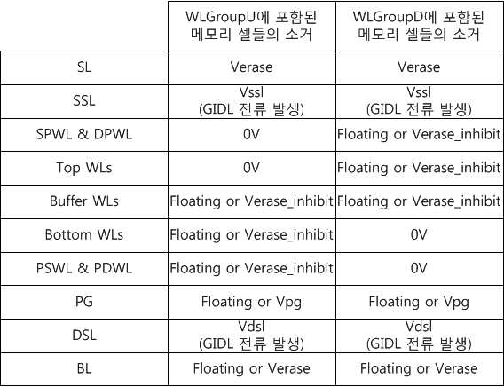
구체적으로 설명하면, 동작 회로(120~140)는 소거 동작을 위해 공통 소스 라인(SL)으로 소거 전압(Verase)을 인가하고, 비트라인들(BL)을 플로팅 상태로 설정하거나 비트라인(BL)에 소거 전압(Verase)을 인가하도록 구성될 수 있다. 또한, 동작 회로(120~140)는 파이프 트랜지스터의 게이트(PG)를 플로팅 상태로 설정하거나 게이트(PG)에 약 10V와 같이 소거를 금지할 수 있는 양전압(Vpg)을 인가하고, 버퍼 워드라인(Buffer WLs)을 플로팅 상태로 설정하거나 버퍼 워드라인(Buffer WLs)에 소거 전압(Verase)보다 낮은 약 10V의 소거 금지 전압(Verase_inhibit)을 인가할 수 있다. 동작 회로(120~140)는 셀렉트 트랜지스터에서 소거 동작에 필요한 GIDL 전류를 발생시키기 위하여 셀레트 라인들(SSL, DSL)에 소거 전압(Verase)보다 약 8V 정도 낮은 양전위의 셀렉트 전압들(Vssl, Vdsl)을 인가할 수 있다. Specifically, the
한편, 상부 워드라인 그룹(WLGroupU)의 워드라인들(Top WLs)과 연결되는 메모리 셀들의 소거 동작을 실시하는 경우, 동작 회로(120~140)는 상부 더미 워드라인들(DPWL, SPWL)과 상부 워드라인들(Top WLs)에 접지 전압(예, 0V)을 인가할 수 있다. 그리고, 동작 회로(120~140)는 하부 더미 워드라인들(PDWL, PSWL)과 하부 워드라인들(Bottom WLs)을 플로팅 상태로 설정하거나 하부 더미 워드라인들(PDWL, PSWL)과 하부 워드라인들(Bottom WLs) 소거 전압(Verase)보다 낮은 약 10V의 소거 금지 전압(Verase_inhibit)을 인가할 수 있다. On the other hand, when performing the erase operation of the memory cells connected to the word lines (Top WLs) of the upper word line group (WLGroupU), the operation circuits (120 to 140) A ground voltage (e.g., 0 V) can be applied to the word lines (Top WLs). The
반대로, 하부 워드라인 그룹(WLGroupD)의 워드라인들(Bottom WLs)과 연결되는 메모리 셀들의 소거 동작을 실시하는 경우, 동작 회로(120~140)는 하부 더미 워드라인들(PDWL, PSWL)과 하부 워드라인들(Bottom WLs)에 접지 전압(예, 0V)을 인가할 수 있다. 그리고, 동작 회로(120~140)는 상부 더미 워드라인들(DPWL, SPWL)과 상부 워드라인들(Top WLs)을 플로팅 상태로 설정하거나 상부 더미 워드라인들(DPWL, SPWL)과 상부 워드라인들(Top WLs) 소거 전압(Verase)보다 낮은 약 10V의 소거 금지 전압(Verase_inhibit)을 인가할 수 있다.
Conversely, when performing the erase operation of the memory cells connected to the word lines (Bottom WLs) of the lower word line group (WLGroupD), the operation circuits (120-140) are connected to the lower dummy word lines (PDWL, PSWL) A ground voltage (e.g., 0 V) may be applied to the word lines Bottom WLs. The
도 1 및 도 8을 참조하면, 기판 상에 적층되는 메모리 셀들은 위치에 따라 다수의 그룹들(WLGroupD, WLGRoupS)로 구분될 수 있다. 즉, 드레인 셀렉트 라인(DSL)과 기판 사이에 위치하는 워드라인들(WLd)과 연결되는 메모리 셀들이 제1 그룹(WLGroupD)이 되고, 소스 셀렉트 라인(SSL)과 기판 사이에 위치하는 워드라인들(WLs)과 연결되는 메모리 셀들이 제2 그룹(WLGroupS)이 될 수 있다. Referring to FIGS. 1 and 8, memory cells stacked on a substrate may be divided into a plurality of groups WLGroupD and WLGRoupS depending on positions. That is, the memory cells connected to the word lines WLd located between the drain select line DSL and the substrate become the first group WLGroupD, and the word lines WL located between the source select line SSL and the substrate And the memory cells connected to the word lines WLs may be the second group WLGroupS.
드레인 셀렉트 라인(DSL)과 연결되는 셀렉트 트랜지스터와 워드라인 그룹(WLd)의 메모리 셀들 사이에는 더미 워드라인(DPWL)과 연결되는 더미 셀이 연결될 수 있다. 소스 셀렉트 라인(SSL)과 연결되는 셀렉트 트랜지스터와 워드라인 그룹(WLs)의 메모리 셀들 사이에는 더미 워드라인(SPWL)과 연결되는 더미 셀이 연결될 수 있다. A dummy cell connected to the dummy word line (DPWL) may be connected between the select transistor connected to the drain select line (DSL) and the memory cells of the word line group (WLd). A dummy cell connected to the dummy word line (SPWL) may be connected between the memory cell of the select transistor connected to the source select line (SSL) and the word line group (WLs).
또한, 파이프 게이트 라인(PG)과 연결되는 파이프 트랜지스터와 워드라인 그룹(WLd)의 메모리 셀들 사이에는 더미 워드라인(PDWL)과 연결되는 더미 셀이 연결될 수 있다. 파이프 게이트 라인(PG)과 연결되는 파이프 트랜지스터와 워드라인 그룹(WLs)의 메모리 셀들 사이에는 더미 워드라인(PSWL)과 연결되는 더미 셀이 연결될 수 있다. A dummy cell connected to the dummy word line PDWL may be connected between the pipe transistor connected to the pipe gate line PG and the memory cells of the word line group WLd. A dummy cell connected to the dummy word line (PSWL) may be connected between the memory cell of the word line group WLs and the pipe transistor connected to the pipe gate line PG.
선택된 그룹의 워드라인들과 연결되는 메모리 셀들의 소거 동작을 실시하기 위하여, 동작 회로(120~140)는 비트라인들(BL), 공통 소스 라인(SL) 및 로컬 라인들(SSL, DPWL, SPWL, WLs, WLd, PDWL, PSWL, DSL, PG)로 하기의 표 6에서와 같이 소거 동작에 필요한 전압들을 인가할 수 있다. In order to perform the erase operation of the memory cells connected to the selected group of word lines, the
[표 6][Table 6]

구체적으로 설명하면, 제1 실시예의 경우, 동작 회로(120~140)는 소거 동작을 위해 공통 소스 라인(SL)과 비트라인(BL)으로 소거 전압(Verase)을 인가하고, 소스 셀렉트 라인(SSL)에는 소스 셀렉트 트랜지스터에서 소거 동작에 필요한 GIDL 전류를 발생시키기 위하여 소거 전압(Verase)보다 약 8V 정도 낮은 양전위의 소스 셀렉트 전압(Vssl)을 인가할 수 있다. 드레인 셀렉트 라인(DSL)에는 소거 디스터번스 특성을 개선하기 위하여 소거 전압(Verase)보다 약 5V 정도 낮은 양전위의 드레인 셀렉트 전압(Vdsl)이 인가될 수 있다. 파이프 트랜지스터의 파이프 게이트(PG)는 플로팅 상태로 설정되거나 파이프 게이트(PG)에 소거 금지 전압(Verase_inhibit)이 인가될 수 있다. More specifically, in the case of the first embodiment, the
상기의 조건에서 그룹(WLGroupS)에 포함된 메모리 셀들의 소거 동작을 실시하는 경우, 동작 회로(120~140)는 더미 워드라인들(SPWL, PSWL)과 워드라인들(WLs)에 소거를 위한 접지 전압(예, 0V)을 인가할 수 있다. 이때, 더미 워드라인(PSWL)은 플로팅 상태로 설정될 수도 있다. 또한, 동작 회로(120~140)는 더미 워드라인들(DPWL, PDWL)과 워드라인들(WLd)을 플로팅 상태로 설정하거나 더미 워드라인들(DPWL, PDWL)과 워드라인들(WLd)에 소거 금지 전압(Verase_inhibit)을 인가할 수 있다. When performing the erase operation of the memory cells included in the group WLGroupS under the above conditions, the
반대로, 그룹(WLGroupD)에 포함된 메모리 셀들의 소거 동작을 실시하는 경우, 동작 회로(120~140)는 더미 워드라인들(DPWL, PDWL)과 워드라인들(WLd)에 소거를 위한 접지 전압(예, 0V)을 인가할 수 있다. 이때, 더미 워드라인(PDWL)은 플로팅 상태로 설정될 수도 있다. 또한, 동작 회로(120~140)는 더미 워드라인들(SPWL, PSWL)과 워드라인들(WLs)을 플로팅 상태로 설정하거나 더미 워드라인들(SPWL, PSWL)과 워드라인들(WLs)에 소거 금지 전압(Verase_inhibit)을 인가할 수 있다. Conversely, when performing the erase operation of the memory cells included in the group WLGroupD, the operation circuit 120-140 outputs the ground voltage (for erasing) to the dummy word lines DPWL and PDWL and the word lines WLd (For example, 0 V) can be applied. At this time, the dummy word line PDWL may be set to the floating state. The
제2 실시예의 경우, 동작 회로(120~140)는 소거 동작을 위해 공통 소스 라인(SL)과 비트라인(BL)으로 소거 전압(Verase)을 인가하고, 파이프 트랜지스터를 턴오프시키기 위한 전압(Vpg)을 파이프 트랜지스터의 파이프 게이트(PG)로 인가할 수 있다. In the case of the second embodiment, the
상기의 조건에서 그룹(WLGroupS)에 포함된 메모리 셀들의 소거 동작을 실시하는 경우, 동작 회로(120~140)는 더미 워드라인들(SPWL, PSWL)과 워드라인들(WLs)에 소거를 위한 접지 전압(예, 0V)을 인가할 수 있다. 이때, 더미 워드라인(PSWL)은 플로팅 상태로 설정될 수도 있다. 또한, 동작 회로(120~140)는 더미 워드라인들(DPWL, PDWL)과 워드라인들(WLd)을 플로팅 상태로 설정하거나 더미 워드라인들(DPWL, PDWL)과 워드라인들(WLd)에 소거 금지 전압(Verase_inhibit)을 인가할 수 있다. When performing the erase operation of the memory cells included in the group WLGroupS under the above conditions, the
제1 실시예와 달리, 동작 회로(120~140)는 소스 셀렉트 트랜지스터에서 소거 동작에 필요한 GIDL 전류를 발생시키기 위하여 소거 전압(Verase)보다 약 8V 정도 낮은 양전위의 소스 셀렉트 전압(Vssl)을 소스 셀렉트 라인(SSL)에 인가할 수 있다. 또한, 드레인 셀렉트 라인(DSL)에는 소거 디스터번스 특성을 개선하기 위하여 소거 전압(Verase)보다 약 5V 정도 낮은 양전위의 드레인 셀렉트 전압(Vdsl)이 인가될 수 있다. Unlike the first embodiment, the
그룹(WLGroupD)에 포함된 메모리 셀들의 소거 동작을 실시하는 경우, 동작 회로(120~140)는 더미 워드라인들(DPWL, PDWL)과 워드라인들(WLd)에 소거를 위한 접지 전압(예, 0V)을 인가할 수 있다. 이때, 더미 워드라인(PDWL)은 플로팅 상태로 설정될 수도 있다. 또한, 동작 회로(120~140)는 더미 워드라인들(SPWL, PSWL)과 워드라인들(WLs)을 플로팅 상태로 설정하거나 더미 워드라인들(SPWL, PSWL)과 워드라인들(WLs)에 소거 금지 전압(Verase_inhibit)을 인가할 수 있다. When performing the erase operation of the memory cells included in the group WLGroupD, the operation circuit 120-140 sets the ground voltage (for example, the erase voltage for erasing) to the dummy word lines DPWL and PDWL and the word lines WLd, 0V) can be applied. At this time, the dummy word line PDWL may be set to the floating state. The
제1 실시예와 달리, 동작 회로(120~140)는 드레인 셀렉트 트랜지스터에서 소거 동작에 필요한 GIDL 전류를 발생시키기 위하여 소거 전압(Verase)보다 약 8V 정도 낮은 양전위의 드레인 셀렉트 전압(Vdsl)을 드레인 셀렉트 라인(DSL)에 인가할 수 있다. 또한, 소스 셀렉트 라인(SSL)에는 소거 디스터번스 특성을 개선하기 위하여 소거 전압(Verase)보다 약 5V 정도 낮은 양전위의 소스 셀렉트 전압(Vssl)이 인가될 수 있다. Unlike the first embodiment, the
도 3 내지 도 8과 표 1 내지 표 6을 참조하여 설명한 방식에 따라 소거 동작을 실시함으로써, 메모리 블록보다 작고 다양한 단위로 소거 동작을 실시할 수 있다.
By performing the erase operation in accordance with the method described with reference to Figs. 3 to 8 and Tables 1 to 6, the erase operation can be performed in units smaller than the memory block.
도 9는 본 발명의 실시예에 따른 메모리 시스템을 간략히 보여주는 블록도이다. 9 is a block diagram briefly showing a memory system according to an embodiment of the present invention.
도 9를 참조하면, 본 발명의 실시예에 따른 메모리 시스템(900)은 불휘발성 메모리 장치(920)와 메모리 컨트롤러(910)를 포함한다.Referring to FIG. 9, a
불휘발성 메모리 장치(920)는 도 1에서 설명한 메모리 장치에 해당할 수 있으며, 도 1에서 설명한 바와 같이 메모리 어레이와 동작 회로가 연결될 수 있다. 메모리 컨트롤러(910)는 불휘발성 메모리 장치(920)를 제어하도록 구성될 것이다. 불휘발성 메모리 장치(920)와 메모리 컨트롤러(910)의 결합에 의해 메모리 카드 또는 반도체 디스크 장치(Solid State Disk: SSD)로 제공될 수 있을 것이다. SRAM(911)은 프로세싱 유닛(912)의 동작 메모리로써 사용된다. 호스트 인터페이스(913)는 메모리 시스템(900)과 접속되는 호스트의 데이터 교환 프로토콜을 구비한다. 에러 정정 블록(914)은 불휘발성 메모리 장치(920)의 셀 영역으로부터 독출된 데이터에 포함되는 에러를 검출 및 정정한다. 메모리 인터페이스(914)는 본 발명의 불휘발성 메모리 장치(920)와 인터페이싱 한다. 프로세싱 유닛(912)은 메모리 컨트롤러(910)의 데이터 교환을 위한 제반 제어 동작을 수행한다.The
비록 도면에는 도시되지 않았지만, 본 발명에 따른 메모리 시스템(900)은 호스트(Host)와의 인터페이싱을 위한 코드 데이터를 저장하는 ROM(미도시됨) 등이 더 제공될 수 있음은 이 분야의 통상적인 지식을 습득한 자들에게 자명하다. 불휘발성 메모리 장치(920)는 복수의 플래시 메모리 칩들로 구성되는 멀티-칩 패키지로 제공될 수도 있다. 이상의 본 발명의 메모리 시스템(900)은 동작 특성이 향상된 고신뢰성의 저장 매체로 제공될 수 있다. 특히, 최근 활발히 연구되고 있는 반도체 디스크 장치(Solid State Disk: 이하 SSD)와 같은 메모리 시스템에서 본 발명의 플래시 메모리 장치가 구비될 수 있다. 이 경우, 메모리 컨트롤러(910)는 USB, MMC, PCI-E, SATA, PATA, SCSI, ESDI, 그리고 IDE 등과 같은 다양한 인터페이스 프로토콜들 중 하나를 통해 외부(예를 들면, 호스트)와 통신하도록 구성될 것이다.
Although not shown in the figure, the
도 10은 프로그램 동작을 수행하는 퓨전 메모리 장치 또는 퓨전 메모리 시스템을 간략히 보여주는 블록도이다. 예를 들면, 퓨전 메모리 장치로서 원낸드 플래시 메모리 장치(1000)에 본 발명의 기술적 특징이 적용될 수 있다.10 is a block diagram briefly showing a fusion memory device or a fusion memory system performing a program operation. For example, the technical features of the present invention can be applied to the one-nAND
원낸드 플래시 메모리 장치(1000)는 서로 다른 프로토콜을 사용하는 장치와의 각종 정보 교환을 위한 호스트 인터페이스(1010)와, 메모리 장치를 구동하기 위한 코드를 내장하거나 데이터를 일시적으로 저장하는 버퍼 램(1020)과, 외부에서 주어지는 제어 신호와 명령어에 응답하여 읽기와 프로그램 및 모든 상태를 제어하는 제어부(1030)와, 명령어와 어드레스, 메모리 장치 내부의 시스템 동작 환경을 정의하는 설정(Configuration) 등의 데이터가 저장되는 레지스터(1040) 및 불휘발성 메모리 셀과 페이지 버퍼를 포함하는 동작 회로로 구성된 낸드 플래시 셀 어레이(1050)를 포함한다. 호스트로부터의 쓰기 요청에 응답하여 원낸드 플래시 메모리 장치는 일반적인 방식에 따라 데이터를 프로그램하게 된다.
The one-NAND
도 11에는 본 발명에 따른 플래시 메모리 장치(1112)를 포함한 컴퓨팅 시스템이 개략적으로 도시되어 있다.11, a computing system including a
본 발명에 따른 컴퓨팅 시스템(1100)은 시스템 버스(1160)에 전기적으로 연결된 마이크로프로세서(1120), 램(1130), 사용자 인터페이스(1140), 베이스밴드 칩셋(Baseband chipset)과 같은 모뎀(1150) 및 메모리 시스템(1110)을 포함한다. 본 발명에 따른 컴퓨팅 시스템(1100)이 모바일 장치인 경우, 컴퓨팅 시스템(1100)의 동작 전압을 공급하기 위한 배터리(미도시됨)가 추가적으로 제공될 것이다. 비록 도면에는 도시되지 않았지만, 본 발명에 따른 컴퓨팅 시스템(1100)에는 응용 칩셋(Application chipset), 카메라 이미지 프로세서(Camera Image Processor: CIS), 모바일 디램, 등이 더 제공될 수 있음은 이 분야의 통상적인 지식을 습득한 자들에게 자명하다. 메모리 시스템(1110)은, 예를 들면, 데이터를 저장하기 위해 도 1에서 설명한 불휘발성 메모리를 사용하는 SSD(Solid State Drive/Disk)를 구성할 수 있다. 또는, 메모리 시스템(1110)은, 퓨전 플래시 메모리(예를 들면, 원낸드 플래시 메모리)로 제공될 수 있다.
The
110 : 메모리 어레이
110MB : 메모리 블록
ST : 메모리 스트링
120 : 제어 회로
130 : 전압 공급 회로
140 : 읽기/쓰기 회로110:
ST: memory string 120: control circuit
130: voltage supply circuit 140: read / write circuit
Claims (16)
상기 메모리 스트링에 포함된 메모리 셀들의 소거 동작을 실시하도록 구성된 동작 회로를 포함하며,
상기 비트라인들이 다수의 그룹들로 구분되고,
상기 동작 회로는 상기 소거 동작을 위해 선택된 그룹의 비트라인들로 소거 전압을 인가하고 상기 공통 소스 라인을 플로팅 상태로 설정하도록 구성되는 반도체 장치.
A memory block including memory strings connected respectively to bit lines formed on a substrate and connected in common with a common source line formed on the substrate; And
And an operation circuit configured to perform an erase operation of the memory cells included in the memory string,
The bit lines are divided into a plurality of groups,
Wherein the operating circuit is configured to apply an erase voltage to the bit lines selected for the erase operation and set the common source line to a floating state.
상기 비트라인들은 배열된 순서에 따라 다수의 그룹들로 구분되고,
상기 동작 회로는 비선택 그룹의 비트라인들에 상기 소거 전압보다 낮은 소거 금지 전압을 인가하도록 구성되는 반도체 장치.
The method according to claim 1,
The bit lines are divided into a plurality of groups according to the arranged order,
Wherein the operation circuit is configured to apply a erase inhibit voltage lower than the erase voltage to the bit lines of the unselected group.
상기 동작 회로는 상기 소거 동작을 실시할 때 상기 그룹들 사이에 위치하는 버퍼 비트라인들을 플로팅 상태로 설정하거나 상기 소거 전압보다 낮은 양전압을 인가하도록 구성되는 반도체 장치.
3. The method of claim 2,
Wherein the operating circuit is configured to set buffer bit lines located between the groups to a floating state when applying the erase operation or to apply a positive voltage lower than the erase voltage.
상기 비트라인들은 이븐 비트라인들을 포함하는 그룹과 오드 비트라인들을 포함하는 그룹으로 구분되고,
상기 동작 회로는 비선택 그룹의 비트라인들에 상기 소거 전압보다 낮은 소거 금지 전압을 인가하거나 상기 비선택 그룹의 비트라인들을 플로팅 상태로 설정하도록 구성되는 반도체 장치.
The method according to claim 1,
Wherein the bit lines are divided into groups including odd bit lines and odd bit lines,
Wherein the operation circuit is configured to apply a erase inhibit voltage lower than the erase voltage to the bit lines of the unselected group or set the bit lines of the unselected group to a floating state.
상기 메모리 스트링은 상기 비트라인과 연결되는 드레인 셀렉트 트랜지스터, 상기 공통 소스 라인과 연결되는 소스 셀렉트 트랜지스터 및 상기 드레인 셀렉트 트랜지스터와 상기 소스 셀렉트 트랜지스터의 사이에 연결되는 상기 메모리 셀들을 포함하며,
상기 동작 회로는 상기 공통 소스 라인과 상기 소스 셀렉트 트랜지스터를 플로팅 상태로 설정하고, 상기 드레인 셀렉트 트랜지스터에 GIDL 전류를 발생시키기 위한 양전압을 인가하도록 구성되는 반도체 장치.
The method according to claim 1,
The memory string including a drain select transistor coupled to the bit line, a source select transistor coupled to the common source line, and memory cells coupled between the drain select transistor and the source select transistor,
Wherein the operation circuit is configured to set the common source line and the source select transistor to a floating state and apply a positive voltage for generating a GIDL current to the drain select transistor.
상기 메모리 스트링은 상기 기판에 형성된 파이프 트랜지스터를 포함하며,
상기 동작 회로는 상기 소거 동작 시 상기 파이프 트랜지스터를 소거 금지 상태로 설정하도록 구성되는 반도체 장치.
The method according to claim 1,
Wherein the memory string comprises a pipe transistor formed in the substrate,
Wherein the operation circuit is configured to set the pipe transistor to an erase prohibition state in the erase operation.
상기 메모리 셀들의 소거 동작을 실시하도록 구성된 동작 회로를 포함하며,
상기 소스 셀렉트 트랜지스터들의 게이트들이 서로 연결되는 한 쌍의 인접한 메모리 스트링들이 하나의 그룹으로 정의되고,
상기 동작 회로는 선택된 그룹의 메모리 스트링들에 포함된 메모리 셀들의 소거 동작을 실시하도록 구성되는 반도체 장치.
And a memory string connected vertically from the substrate between a bit line formed on the substrate and a common source line, the memory string including a drain select transistor connected between the bit line and the common source line, memory cells and source select A memory block including a transistor; And
And an operation circuit configured to perform an erase operation of the memory cells,
A pair of adjacent memory strings in which gates of the source select transistors are connected to each other are defined as one group,
Wherein the operating circuit is configured to perform an erase operation of the memory cells included in the selected group of memory strings.
상기 동작 회로는 상기 소거 동작을 위해 상기 공통 소스 라인으로 소거 전압을 인가하고, 상기 비트라인을 플로팅 상태로 설정하거나 상기 비트라인에 상기 소거 전압을 인가하도록 구성되는 반도체 장치.
8. The method of claim 7,
Wherein the operating circuit is configured to apply an erase voltage to the common source line for the erase operation and to set the bit line to a floating state or to apply the erase voltage to the bit line.
상기 동작 회로는 상기 선택된 그룹의 상기 소스 셀렉트 트랜지스터들의 상기 게이트들로 GIDL 전류를 발생시키기 위한 제1 양전압을 인가하고,
비선택된 그룹들의 상기 소스 셀렉트 트랜지스터들의 상기 게이트들로 상기 제1 양전압보다 낮은 제2 양전압을 인가하거나 상기 비선택된 그룹들의 상기 소스 셀렉트 트랜지스터들의 상기 게이트들을 플로팅 상태로 설정하도록 구성되는 반도체 장치.
8. The method of claim 7,
The operating circuit applies a first positive voltage for generating a GIDL current to the gates of the source select transistors of the selected group,
And apply a second positive voltage lower than the first positive voltage to the gates of the source select transistors of the non-selected groups or to set the gates of the source select transistors of the non-selected groups to a floating state.
상기 동작 회로는 상기 선택된 그룹의 상기 드레인 셀렉트 트랜지스터들의 게이트들로 GIDL 전류를 발생시키기 위한 제1 양전압을 인가하고,
비선택된 그룹들의 상기 드레인 셀렉트 트랜지스터들의 게이트들로 상기 제1 양전압보다 낮은 제2 양전압을 인가하거나 상기 비선택된 그룹들의 상기 드레인 셀렉트 트랜지스터들의 상기 게이트들을 플로팅 상태로 설정하도록 구성되는 반도체 장치.
8. The method of claim 7,
The operating circuit applies a first positive voltage for generating a GIDL current to the gates of the selected group of drain select transistors,
And apply a second positive voltage lower than the first positive voltage to the gates of the drain select transistors of the non-selected groups or set the gates of the drain select transistors of the non-selected groups to a floating state.
상기 메모리 스트링은 상기 메모리 셀들 사이에 연결되고 상기 기판에 형성되는 파이프 트랜지스터를 포함하며,
상기 동작 회로는 상기 소거 동작 시 상기 파이프 트랜지스터의 게이트에 소거를 금지할 수 있는 양전압이나 상기 파이프 트랜지스터의 상기 게이트를 플로팅 상태로 설정하도록 구성되는 반도체 장치.
8. The method of claim 7,
The memory string including a pipe transistor connected between the memory cells and formed in the substrate,
Wherein the operation circuit is configured to set a positive voltage capable of inhibiting erasure of the gate of the pipe transistor during the erase operation or the gate of the pipe transistor to a floating state.
상기 메모리 셀들의 소거 동작을 실시하도록 구성된 동작 회로를 포함하며,
서로 다른 비트라인들에 연결되고 드레인 셀렉트 트랜지스터들의 게이트들을 공유하는 메모리 스트링들이 하나의 그룹으로 정의되고,
상기 동작 회로는 선택된 그룹의 메모리 스트링들에 포함된 메모리 셀들의 소거 동작을 실시하도록 구성되는 반도체 장치.
And a memory string connected vertically from the substrate between bit lines formed on a substrate and a common source line, the memory string including a drain select transistor connected between the bit line and the common source line, A memory block including a select transistor; And
And an operation circuit configured to perform an erase operation of the memory cells,
Memory strings connected to different bit lines and sharing the gates of the drain select transistors are defined as a group,
Wherein the operating circuit is configured to perform an erase operation of the memory cells included in the selected group of memory strings.
상기 동작 회로는 상기 소거 동작을 위해 상기 비트 라인들로 소거 전압을 인가하고, 상기 공통 소스 라인은 플로팅 상태로 설정하도록 구성되는 반도체 장치.
13. The method of claim 12,
Wherein the operating circuit is configured to apply an erase voltage to the bit lines for the erase operation and to set the common source line to a floating state.
상기 동작 회로는 상기 선택된 그룹의 상기 드레인 셀렉트 트랜지스터들의 상기 게이트들로 GIDL 전류를 발생시키기 위한 제1 양전압을 인가하고,
상기 선택된 그룹의 상기 소스 셀렉트 트랜지스터들의 상기 게이트들을 플로팅 상태로 설정하도록 구성되는 반도체 장치.
13. The method of claim 12,
The operation circuit applies a first positive voltage for generating a GIDL current to the gates of the selected group of drain select transistors,
And to set the gates of the source select transistors of the selected group to a floating state.
상기 동작 회로는 비선택된 그룹의 상기 드레인 셀렉트 트랜지스터들의 상기 게이트들로 소거 디스터번스 특성을 개선하기 위한 제2 양전압을 인가하거나 상기 비선택된 그룹들의 상기 소스 셀렉트 트랜지스터들의 상기 게이트들을 플로팅 상태로 설정하고,
상기 비선택된 그룹의 상기 소스 셀렉트 트랜지스터들의 상기 게이트들을 플로팅 상태로 설정하도록 구성되는 반도체 장치.
13. The method of claim 12,
The operation circuit applies a second positive voltage to improve the erase disturbance characteristic to the gates of the drain select transistors of a non-selected group or sets the gates of the source select transistors of the non-selected groups to a floating state,
And set the gates of the source select transistors of the non-selected group to a floating state.
상기 메모리 스트링은 상기 메모리 셀들 사이에 연결되고 상기 기판에 형성되는 파이프 트랜지스터를 포함하며,
상기 동작 회로는 상기 소거 동작 시 상기 파이프 트랜지스터의 게이트에 소거를 금지할 수 있는 양전압이나 상기 파이프 트랜지스터의 상기 게이트를 플로팅 상태로 설정하도록 구성되는 반도체 장치. 13. The method of claim 12,
The memory string including a pipe transistor connected between the memory cells and formed in the substrate,
Wherein the operation circuit is configured to set a positive voltage capable of inhibiting erasure of the gate of the pipe transistor during the erase operation or the gate of the pipe transistor to a floating state.
Priority Applications (2)
| Application Number | Priority Date | Filing Date | Title |
|---|---|---|---|
| KR1020140161654A KR20160059745A (en) | 2014-11-19 | 2014-11-19 | Semiconductor appratus |
| US14/691,827 US9875800B2 (en) | 2014-11-19 | 2015-04-21 | 3D NAND semiconductor device for erasing groups of bit lines |
Applications Claiming Priority (1)
| Application Number | Priority Date | Filing Date | Title |
|---|---|---|---|
| KR1020140161654A KR20160059745A (en) | 2014-11-19 | 2014-11-19 | Semiconductor appratus |
Publications (1)
| Publication Number | Publication Date |
|---|---|
| KR20160059745A true KR20160059745A (en) | 2016-05-27 |
Family
ID=55962288
Family Applications (1)
| Application Number | Title | Priority Date | Filing Date |
|---|---|---|---|
| KR1020140161654A Withdrawn KR20160059745A (en) | 2014-11-19 | 2014-11-19 | Semiconductor appratus |
Country Status (2)
| Country | Link |
|---|---|
| US (1) | US9875800B2 (en) |
| KR (1) | KR20160059745A (en) |
Cited By (4)
| Publication number | Priority date | Publication date | Assignee | Title |
|---|---|---|---|---|
| KR20180087809A (en) * | 2017-01-25 | 2018-08-02 | 삼성전자주식회사 | Non-volatile memory device and method of programming the same |
| US10347339B2 (en) | 2016-11-28 | 2019-07-09 | SK Hynix Inc. | Semiconductor memory device and operating method thereof |
| KR20190109122A (en) * | 2018-03-16 | 2019-09-25 | 에스케이하이닉스 주식회사 | Memory device and memory system having the same |
| KR20190142550A (en) * | 2018-06-18 | 2019-12-27 | 삼성전자주식회사 | Nonvolatile memory device comprising erase control circuit |
Families Citing this family (11)
| Publication number | Priority date | Publication date | Assignee | Title |
|---|---|---|---|---|
| KR102320830B1 (en) * | 2015-09-24 | 2021-11-03 | 에스케이하이닉스 주식회사 | Semiconductor memory device including three-dimensional array structure |
| US10170188B1 (en) * | 2017-08-31 | 2019-01-01 | Micron Technology, Inc. | 3D memory device including shared select gate connections between memory blocks |
| KR102701788B1 (en) * | 2018-09-28 | 2024-08-30 | 삼성전자주식회사 | A memory device and a storage system using the same |
| US10964398B2 (en) * | 2018-09-28 | 2021-03-30 | Samsung Electronics Co., Ltd. | Memory device and a storage system using the same |
| US11061617B2 (en) | 2019-02-20 | 2021-07-13 | Marvell Asia Pte, Ltd. | High density fractional bit solid state drives using coded set partitions |
| JP2021140853A (en) * | 2020-03-09 | 2021-09-16 | キオクシア株式会社 | Semiconductor storage device |
| KR102897358B1 (en) | 2020-07-30 | 2025-12-05 | 삼성전자 주식회사 | Two way precharge during programming in non-volatile memory device |
| KR20220099063A (en) * | 2021-01-05 | 2022-07-12 | 에스케이하이닉스 주식회사 | Semiconductor memory device and operating method thereof |
| CN114613415B (en) * | 2022-03-03 | 2026-04-21 | 长江存储科技有限责任公司 | Non-volatile memory, memory systems, and memory data erasure methods |
| KR20250012884A (en) | 2023-07-18 | 2025-01-31 | 삼성전자주식회사 | Nonvolatile memory device, storage device having the same, and operating method thereof |
| US20260011377A1 (en) * | 2024-07-02 | 2026-01-08 | Macronix International Co., Ltd. | Erase method for memory device and memory device |
Family Cites Families (9)
| Publication number | Priority date | Publication date | Assignee | Title |
|---|---|---|---|---|
| KR101658479B1 (en) * | 2010-02-09 | 2016-09-21 | 삼성전자주식회사 | Nonvolatile memory device, operating method thereof and memory system including the same |
| KR101691092B1 (en) | 2010-08-26 | 2016-12-30 | 삼성전자주식회사 | Nonvolatile memory device, operating method thereof and memory system including the same |
| KR20120058380A (en) | 2010-11-29 | 2012-06-07 | 가부시끼가이샤 도시바 | Nonvolatile semiconductor memory device and control method thereof |
| US8787094B2 (en) * | 2012-04-18 | 2014-07-22 | Sandisk Technologies Inc. | Soft erase operation for 3D non-volatile memory with selective inhibiting of passed bits |
| KR20140020628A (en) * | 2012-08-10 | 2014-02-19 | 에스케이하이닉스 주식회사 | Semiconductor memory device |
| KR101997912B1 (en) | 2012-08-30 | 2019-07-08 | 에스케이하이닉스 주식회사 | Semiconductor memory device and method of operating the same |
| US9224474B2 (en) * | 2013-01-09 | 2015-12-29 | Macronix International Co., Ltd. | P-channel 3D memory array and methods to program and erase the same at bit level and block level utilizing band-to-band and fowler-nordheim tunneling principals |
| US8923054B1 (en) * | 2013-06-14 | 2014-12-30 | Sandisk Technologies Inc. | Pseudo block operation mode in 3D NAND |
| US9286984B2 (en) * | 2014-07-07 | 2016-03-15 | Macronix International Co., Ltd. | Reduced size semiconductor device and method for manufacture thereof |
-
2014
- 2014-11-19 KR KR1020140161654A patent/KR20160059745A/en not_active Withdrawn
-
2015
- 2015-04-21 US US14/691,827 patent/US9875800B2/en active Active
Cited By (4)
| Publication number | Priority date | Publication date | Assignee | Title |
|---|---|---|---|---|
| US10347339B2 (en) | 2016-11-28 | 2019-07-09 | SK Hynix Inc. | Semiconductor memory device and operating method thereof |
| KR20180087809A (en) * | 2017-01-25 | 2018-08-02 | 삼성전자주식회사 | Non-volatile memory device and method of programming the same |
| KR20190109122A (en) * | 2018-03-16 | 2019-09-25 | 에스케이하이닉스 주식회사 | Memory device and memory system having the same |
| KR20190142550A (en) * | 2018-06-18 | 2019-12-27 | 삼성전자주식회사 | Nonvolatile memory device comprising erase control circuit |
Also Published As
| Publication number | Publication date |
|---|---|
| US20160141043A1 (en) | 2016-05-19 |
| US9875800B2 (en) | 2018-01-23 |
Similar Documents
| Publication | Publication Date | Title |
|---|---|---|
| KR20160059745A (en) | Semiconductor appratus | |
| KR101897826B1 (en) | Semiconductor memory device and method of operating the same | |
| KR101997912B1 (en) | Semiconductor memory device and method of operating the same | |
| US9299447B2 (en) | 3-dimensional semiconductor device having memory cells stacked over substrate | |
| KR20140020628A (en) | Semiconductor memory device | |
| US9633737B2 (en) | Semiconductor device | |
| TWI633554B (en) | Semiconductor device | |
| KR101951046B1 (en) | Semiconductor memory device, operating method thereof and memory system including thesame | |
| TWI633550B (en) | Semiconductor device | |
| KR20160071948A (en) | Semiconductor apparatus | |
| KR20160107549A (en) | Semiconductor apparatus | |
| US10210937B2 (en) | Semiconductor storage device with multiple blocks | |
| KR20150033129A (en) | Semiconductor memory apparatus | |
| KR20150014680A (en) | Semiconductor memory apparatus | |
| KR20150091687A (en) | Semiconductor apparatus | |
| US9564220B2 (en) | Semiconductor device | |
| US9859010B2 (en) | 3D multi-layer non-volatile memory device with planar string and method of programming | |
| KR20160061765A (en) | Semiconductor apparatus | |
| KR20160031907A (en) | Semiconductor apparatus | |
| KR20160071946A (en) | Semiconductor memory apparatus | |
| KR20160043747A (en) | Semiconductor apparatus | |
| US20160232975A1 (en) | Semiconductor memory device and programming method of the same | |
| US9424935B2 (en) | Semiconductor device | |
| KR20160069354A (en) | Semiconductor apparatus | |
| KR20160037594A (en) | Semiconductor apparatus |
Legal Events
| Date | Code | Title | Description |
|---|---|---|---|
| PA0109 | Patent application |
Patent event code: PA01091R01D Comment text: Patent Application Patent event date: 20141119 |
|
| PG1501 | Laying open of application | ||
| PC1203 | Withdrawal of no request for examination | ||
| WITN | Application deemed withdrawn, e.g. because no request for examination was filed or no examination fee was paid |