KR20140074816A - Dicing tape integrated adhesive sheet, manufacturing method of semiconductor device using dicing tape integrated adhesive sheet, and semiconductor device - Google Patents
Dicing tape integrated adhesive sheet, manufacturing method of semiconductor device using dicing tape integrated adhesive sheet, and semiconductor device Download PDFInfo
- Publication number
- KR20140074816A KR20140074816A KR1020130121712A KR20130121712A KR20140074816A KR 20140074816 A KR20140074816 A KR 20140074816A KR 1020130121712 A KR1020130121712 A KR 1020130121712A KR 20130121712 A KR20130121712 A KR 20130121712A KR 20140074816 A KR20140074816 A KR 20140074816A
- Authority
- KR
- South Korea
- Prior art keywords
- dicing tape
- adhesive sheet
- semiconductor
- pressure
- sensitive adhesive
- Prior art date
- Legal status (The legal status is an assumption and is not a legal conclusion. Google has not performed a legal analysis and makes no representation as to the accuracy of the status listed.)
- Granted
Links
Images


Classifications
-
- C—CHEMISTRY; METALLURGY
- C09—DYES; PAINTS; POLISHES; NATURAL RESINS; ADHESIVES; COMPOSITIONS NOT OTHERWISE PROVIDED FOR; APPLICATIONS OF MATERIALS NOT OTHERWISE PROVIDED FOR
- C09J—ADHESIVES; NON-MECHANICAL ASPECTS OF ADHESIVE PROCESSES IN GENERAL; ADHESIVE PROCESSES NOT PROVIDED FOR ELSEWHERE; USE OF MATERIALS AS ADHESIVES
- C09J7/00—Adhesives in the form of films or foils
- C09J7/30—Adhesives in the form of films or foils characterised by the adhesive composition
- C09J7/38—Pressure-sensitive adhesives [PSA]
-
- H—ELECTRICITY
- H10—SEMICONDUCTOR DEVICES; ELECTRIC SOLID-STATE DEVICES NOT OTHERWISE PROVIDED FOR
- H10P—GENERIC PROCESSES OR APPARATUS FOR THE MANUFACTURE OR TREATMENT OF DEVICES COVERED BY CLASS H10
- H10P72/00—Handling or holding of wafers, substrates or devices during manufacture or treatment thereof
- H10P72/70—Handling or holding of wafers, substrates or devices during manufacture or treatment thereof for supporting or gripping
- H10P72/74—Handling or holding of wafers, substrates or devices during manufacture or treatment thereof for supporting or gripping using temporarily an auxiliary support
- H10P72/7402—Wafer tapes, e.g. grinding or dicing support tapes
-
- C—CHEMISTRY; METALLURGY
- C09—DYES; PAINTS; POLISHES; NATURAL RESINS; ADHESIVES; COMPOSITIONS NOT OTHERWISE PROVIDED FOR; APPLICATIONS OF MATERIALS NOT OTHERWISE PROVIDED FOR
- C09J—ADHESIVES; NON-MECHANICAL ASPECTS OF ADHESIVE PROCESSES IN GENERAL; ADHESIVE PROCESSES NOT PROVIDED FOR ELSEWHERE; USE OF MATERIALS AS ADHESIVES
- C09J7/00—Adhesives in the form of films or foils
- C09J7/40—Adhesives in the form of films or foils characterised by release liners
-
- C—CHEMISTRY; METALLURGY
- C09—DYES; PAINTS; POLISHES; NATURAL RESINS; ADHESIVES; COMPOSITIONS NOT OTHERWISE PROVIDED FOR; APPLICATIONS OF MATERIALS NOT OTHERWISE PROVIDED FOR
- C09J—ADHESIVES; NON-MECHANICAL ASPECTS OF ADHESIVE PROCESSES IN GENERAL; ADHESIVE PROCESSES NOT PROVIDED FOR ELSEWHERE; USE OF MATERIALS AS ADHESIVES
- C09J9/00—Adhesives characterised by their physical nature or the effects produced, e.g. glue sticks
-
- H—ELECTRICITY
- H10—SEMICONDUCTOR DEVICES; ELECTRIC SOLID-STATE DEVICES NOT OTHERWISE PROVIDED FOR
- H10P—GENERIC PROCESSES OR APPARATUS FOR THE MANUFACTURE OR TREATMENT OF DEVICES COVERED BY CLASS H10
- H10P54/00—Cutting or separating of wafers, substrates or parts of devices
-
- H—ELECTRICITY
- H10—SEMICONDUCTOR DEVICES; ELECTRIC SOLID-STATE DEVICES NOT OTHERWISE PROVIDED FOR
- H10P—GENERIC PROCESSES OR APPARATUS FOR THE MANUFACTURE OR TREATMENT OF DEVICES COVERED BY CLASS H10
- H10P72/00—Handling or holding of wafers, substrates or devices during manufacture or treatment thereof
- H10P72/70—Handling or holding of wafers, substrates or devices during manufacture or treatment thereof for supporting or gripping
- H10P72/74—Handling or holding of wafers, substrates or devices during manufacture or treatment thereof for supporting or gripping using temporarily an auxiliary support
- H10P72/7402—Wafer tapes, e.g. grinding or dicing support tapes
- H10P72/7404—Wafer tapes, e.g. grinding or dicing support tapes the wafer tape being a laminate of three or more layers, e.g. including additional layers beyond a base layer and an uppermost adhesive layer
-
- H—ELECTRICITY
- H10—SEMICONDUCTOR DEVICES; ELECTRIC SOLID-STATE DEVICES NOT OTHERWISE PROVIDED FOR
- H10W—GENERIC PACKAGES, INTERCONNECTIONS, CONNECTORS OR OTHER CONSTRUCTIONAL DETAILS OF DEVICES COVERED BY CLASS H10
- H10W46/00—Marks applied to devices, e.g. for alignment or identification
-
- H—ELECTRICITY
- H10—SEMICONDUCTOR DEVICES; ELECTRIC SOLID-STATE DEVICES NOT OTHERWISE PROVIDED FOR
- H10W—GENERIC PACKAGES, INTERCONNECTIONS, CONNECTORS OR OTHER CONSTRUCTIONAL DETAILS OF DEVICES COVERED BY CLASS H10
- H10W72/00—Interconnections or connectors in packages
- H10W72/20—Bump connectors, e.g. solder bumps or copper pillars; Dummy bumps; Thermal bumps
-
- C—CHEMISTRY; METALLURGY
- C09—DYES; PAINTS; POLISHES; NATURAL RESINS; ADHESIVES; COMPOSITIONS NOT OTHERWISE PROVIDED FOR; APPLICATIONS OF MATERIALS NOT OTHERWISE PROVIDED FOR
- C09J—ADHESIVES; NON-MECHANICAL ASPECTS OF ADHESIVE PROCESSES IN GENERAL; ADHESIVE PROCESSES NOT PROVIDED FOR ELSEWHERE; USE OF MATERIALS AS ADHESIVES
- C09J2203/00—Applications of adhesives in processes or use of adhesives in the form of films or foils
- C09J2203/326—Applications of adhesives in processes or use of adhesives in the form of films or foils for bonding electronic components such as wafers, chips or semiconductors
-
- C—CHEMISTRY; METALLURGY
- C09—DYES; PAINTS; POLISHES; NATURAL RESINS; ADHESIVES; COMPOSITIONS NOT OTHERWISE PROVIDED FOR; APPLICATIONS OF MATERIALS NOT OTHERWISE PROVIDED FOR
- C09J—ADHESIVES; NON-MECHANICAL ASPECTS OF ADHESIVE PROCESSES IN GENERAL; ADHESIVE PROCESSES NOT PROVIDED FOR ELSEWHERE; USE OF MATERIALS AS ADHESIVES
- C09J2301/00—Additional features of adhesives in the form of films or foils
- C09J2301/30—Additional features of adhesives in the form of films or foils characterized by the chemical, physicochemical or physical properties of the adhesive or the carrier
- C09J2301/302—Additional features of adhesives in the form of films or foils characterized by the chemical, physicochemical or physical properties of the adhesive or the carrier the adhesive being pressure-sensitive, i.e. tacky at temperatures inferior to 30°C
-
- C—CHEMISTRY; METALLURGY
- C09—DYES; PAINTS; POLISHES; NATURAL RESINS; ADHESIVES; COMPOSITIONS NOT OTHERWISE PROVIDED FOR; APPLICATIONS OF MATERIALS NOT OTHERWISE PROVIDED FOR
- C09J—ADHESIVES; NON-MECHANICAL ASPECTS OF ADHESIVE PROCESSES IN GENERAL; ADHESIVE PROCESSES NOT PROVIDED FOR ELSEWHERE; USE OF MATERIALS AS ADHESIVES
- C09J2301/00—Additional features of adhesives in the form of films or foils
- C09J2301/30—Additional features of adhesives in the form of films or foils characterized by the chemical, physicochemical or physical properties of the adhesive or the carrier
- C09J2301/312—Additional features of adhesives in the form of films or foils characterized by the chemical, physicochemical or physical properties of the adhesive or the carrier parameters being the characterizing feature
-
- C—CHEMISTRY; METALLURGY
- C09—DYES; PAINTS; POLISHES; NATURAL RESINS; ADHESIVES; COMPOSITIONS NOT OTHERWISE PROVIDED FOR; APPLICATIONS OF MATERIALS NOT OTHERWISE PROVIDED FOR
- C09J—ADHESIVES; NON-MECHANICAL ASPECTS OF ADHESIVE PROCESSES IN GENERAL; ADHESIVE PROCESSES NOT PROVIDED FOR ELSEWHERE; USE OF MATERIALS AS ADHESIVES
- C09J2301/00—Additional features of adhesives in the form of films or foils
- C09J2301/40—Additional features of adhesives in the form of films or foils characterized by the presence of essential components
-
- H—ELECTRICITY
- H10—SEMICONDUCTOR DEVICES; ELECTRIC SOLID-STATE DEVICES NOT OTHERWISE PROVIDED FOR
- H10P—GENERIC PROCESSES OR APPARATUS FOR THE MANUFACTURE OR TREATMENT OF DEVICES COVERED BY CLASS H10
- H10P72/00—Handling or holding of wafers, substrates or devices during manufacture or treatment thereof
- H10P72/70—Handling or holding of wafers, substrates or devices during manufacture or treatment thereof for supporting or gripping
- H10P72/74—Handling or holding of wafers, substrates or devices during manufacture or treatment thereof for supporting or gripping using temporarily an auxiliary support
- H10P72/7412—Handling or holding of wafers, substrates or devices during manufacture or treatment thereof for supporting or gripping using temporarily an auxiliary support the auxiliary support including means facilitating the separation of a device or wafer from the auxiliary support
-
- H—ELECTRICITY
- H10—SEMICONDUCTOR DEVICES; ELECTRIC SOLID-STATE DEVICES NOT OTHERWISE PROVIDED FOR
- H10P—GENERIC PROCESSES OR APPARATUS FOR THE MANUFACTURE OR TREATMENT OF DEVICES COVERED BY CLASS H10
- H10P72/00—Handling or holding of wafers, substrates or devices during manufacture or treatment thereof
- H10P72/70—Handling or holding of wafers, substrates or devices during manufacture or treatment thereof for supporting or gripping
- H10P72/74—Handling or holding of wafers, substrates or devices during manufacture or treatment thereof for supporting or gripping using temporarily an auxiliary support
- H10P72/7416—Handling or holding of wafers, substrates or devices during manufacture or treatment thereof for supporting or gripping using temporarily an auxiliary support used during dicing or grinding
- H10P72/742—Handling or holding of wafers, substrates or devices during manufacture or treatment thereof for supporting or gripping using temporarily an auxiliary support used during dicing or grinding involving stretching of the auxiliary support post dicing
-
- H—ELECTRICITY
- H10—SEMICONDUCTOR DEVICES; ELECTRIC SOLID-STATE DEVICES NOT OTHERWISE PROVIDED FOR
- H10P—GENERIC PROCESSES OR APPARATUS FOR THE MANUFACTURE OR TREATMENT OF DEVICES COVERED BY CLASS H10
- H10P72/00—Handling or holding of wafers, substrates or devices during manufacture or treatment thereof
- H10P72/70—Handling or holding of wafers, substrates or devices during manufacture or treatment thereof for supporting or gripping
- H10P72/74—Handling or holding of wafers, substrates or devices during manufacture or treatment thereof for supporting or gripping using temporarily an auxiliary support
- H10P72/7438—Handling or holding of wafers, substrates or devices during manufacture or treatment thereof for supporting or gripping using temporarily an auxiliary support with parts of the auxiliary support remaining in the finished device
-
- H—ELECTRICITY
- H10—SEMICONDUCTOR DEVICES; ELECTRIC SOLID-STATE DEVICES NOT OTHERWISE PROVIDED FOR
- H10W—GENERIC PACKAGES, INTERCONNECTIONS, CONNECTORS OR OTHER CONSTRUCTIONAL DETAILS OF DEVICES COVERED BY CLASS H10
- H10W46/00—Marks applied to devices, e.g. for alignment or identification
- H10W46/401—Marks applied to devices, e.g. for alignment or identification for identification or tracking
-
- H—ELECTRICITY
- H10—SEMICONDUCTOR DEVICES; ELECTRIC SOLID-STATE DEVICES NOT OTHERWISE PROVIDED FOR
- H10W—GENERIC PACKAGES, INTERCONNECTIONS, CONNECTORS OR OTHER CONSTRUCTIONAL DETAILS OF DEVICES COVERED BY CLASS H10
- H10W46/00—Marks applied to devices, e.g. for alignment or identification
- H10W46/601—Marks applied to devices, e.g. for alignment or identification for use after dicing
- H10W46/607—Located on parts of packages, e.g. on encapsulations or on package substrates
-
- H—ELECTRICITY
- H10—SEMICONDUCTOR DEVICES; ELECTRIC SOLID-STATE DEVICES NOT OTHERWISE PROVIDED FOR
- H10W—GENERIC PACKAGES, INTERCONNECTIONS, CONNECTORS OR OTHER CONSTRUCTIONAL DETAILS OF DEVICES COVERED BY CLASS H10
- H10W72/00—Interconnections or connectors in packages
- H10W72/071—Connecting or disconnecting
- H10W72/072—Connecting or disconnecting of bump connectors
- H10W72/07202—Connecting or disconnecting of bump connectors using auxiliary members
-
- H—ELECTRICITY
- H10—SEMICONDUCTOR DEVICES; ELECTRIC SOLID-STATE DEVICES NOT OTHERWISE PROVIDED FOR
- H10W—GENERIC PACKAGES, INTERCONNECTIONS, CONNECTORS OR OTHER CONSTRUCTIONAL DETAILS OF DEVICES COVERED BY CLASS H10
- H10W72/00—Interconnections or connectors in packages
- H10W72/071—Connecting or disconnecting
- H10W72/072—Connecting or disconnecting of bump connectors
- H10W72/07231—Techniques
- H10W72/07236—Soldering or alloying
-
- H—ELECTRICITY
- H10—SEMICONDUCTOR DEVICES; ELECTRIC SOLID-STATE DEVICES NOT OTHERWISE PROVIDED FOR
- H10W—GENERIC PACKAGES, INTERCONNECTIONS, CONNECTORS OR OTHER CONSTRUCTIONAL DETAILS OF DEVICES COVERED BY CLASS H10
- H10W72/00—Interconnections or connectors in packages
- H10W72/071—Connecting or disconnecting
- H10W72/073—Connecting or disconnecting of die-attach connectors
- H10W72/07302—Connecting or disconnecting of die-attach connectors using an auxiliary member
-
- H—ELECTRICITY
- H10—SEMICONDUCTOR DEVICES; ELECTRIC SOLID-STATE DEVICES NOT OTHERWISE PROVIDED FOR
- H10W—GENERIC PACKAGES, INTERCONNECTIONS, CONNECTORS OR OTHER CONSTRUCTIONAL DETAILS OF DEVICES COVERED BY CLASS H10
- H10W72/00—Interconnections or connectors in packages
- H10W72/071—Connecting or disconnecting
- H10W72/073—Connecting or disconnecting of die-attach connectors
- H10W72/07331—Connecting techniques
- H10W72/07337—Connecting techniques using a polymer adhesive, e.g. an adhesive based on silicone or epoxy
- H10W72/07338—Connecting techniques using a polymer adhesive, e.g. an adhesive based on silicone or epoxy hardening the adhesive by curing, e.g. thermosetting
-
- H—ELECTRICITY
- H10—SEMICONDUCTOR DEVICES; ELECTRIC SOLID-STATE DEVICES NOT OTHERWISE PROVIDED FOR
- H10W—GENERIC PACKAGES, INTERCONNECTIONS, CONNECTORS OR OTHER CONSTRUCTIONAL DETAILS OF DEVICES COVERED BY CLASS H10
- H10W72/00—Interconnections or connectors in packages
- H10W72/20—Bump connectors, e.g. solder bumps or copper pillars; Dummy bumps; Thermal bumps
- H10W72/241—Dispositions, e.g. layouts
-
- H—ELECTRICITY
- H10—SEMICONDUCTOR DEVICES; ELECTRIC SOLID-STATE DEVICES NOT OTHERWISE PROVIDED FOR
- H10W—GENERIC PACKAGES, INTERCONNECTIONS, CONNECTORS OR OTHER CONSTRUCTIONAL DETAILS OF DEVICES COVERED BY CLASS H10
- H10W72/00—Interconnections or connectors in packages
- H10W72/20—Bump connectors, e.g. solder bumps or copper pillars; Dummy bumps; Thermal bumps
- H10W72/251—Materials
- H10W72/252—Materials comprising solid metals or solid metalloids, e.g. PbSn, Ag or Cu
-
- H—ELECTRICITY
- H10—SEMICONDUCTOR DEVICES; ELECTRIC SOLID-STATE DEVICES NOT OTHERWISE PROVIDED FOR
- H10W—GENERIC PACKAGES, INTERCONNECTIONS, CONNECTORS OR OTHER CONSTRUCTIONAL DETAILS OF DEVICES COVERED BY CLASS H10
- H10W72/00—Interconnections or connectors in packages
- H10W72/30—Die-attach connectors
- H10W72/321—Structures or relative sizes of die-attach connectors
- H10W72/325—Die-attach connectors having a filler embedded in a matrix
-
- H—ELECTRICITY
- H10—SEMICONDUCTOR DEVICES; ELECTRIC SOLID-STATE DEVICES NOT OTHERWISE PROVIDED FOR
- H10W—GENERIC PACKAGES, INTERCONNECTIONS, CONNECTORS OR OTHER CONSTRUCTIONAL DETAILS OF DEVICES COVERED BY CLASS H10
- H10W72/00—Interconnections or connectors in packages
- H10W72/30—Die-attach connectors
- H10W72/351—Materials of die-attach connectors
- H10W72/353—Materials of die-attach connectors not comprising solid metals or solid metalloids, e.g. ceramics
- H10W72/354—Materials of die-attach connectors not comprising solid metals or solid metalloids, e.g. ceramics comprising polymers
-
- H—ELECTRICITY
- H10—SEMICONDUCTOR DEVICES; ELECTRIC SOLID-STATE DEVICES NOT OTHERWISE PROVIDED FOR
- H10W—GENERIC PACKAGES, INTERCONNECTIONS, CONNECTORS OR OTHER CONSTRUCTIONAL DETAILS OF DEVICES COVERED BY CLASS H10
- H10W74/00—Encapsulations, e.g. protective coatings
- H10W74/01—Manufacture or treatment
- H10W74/012—Manufacture or treatment of encapsulations on active surfaces of flip-chip devices, e.g. forming underfills
-
- H—ELECTRICITY
- H10—SEMICONDUCTOR DEVICES; ELECTRIC SOLID-STATE DEVICES NOT OTHERWISE PROVIDED FOR
- H10W—GENERIC PACKAGES, INTERCONNECTIONS, CONNECTORS OR OTHER CONSTRUCTIONAL DETAILS OF DEVICES COVERED BY CLASS H10
- H10W74/00—Encapsulations, e.g. protective coatings
- H10W74/10—Encapsulations, e.g. protective coatings characterised by their shape or disposition
- H10W74/15—Encapsulations, e.g. protective coatings characterised by their shape or disposition on active surfaces of flip-chip devices, e.g. underfills
-
- H—ELECTRICITY
- H10—SEMICONDUCTOR DEVICES; ELECTRIC SOLID-STATE DEVICES NOT OTHERWISE PROVIDED FOR
- H10W—GENERIC PACKAGES, INTERCONNECTIONS, CONNECTORS OR OTHER CONSTRUCTIONAL DETAILS OF DEVICES COVERED BY CLASS H10
- H10W90/00—Package configurations
- H10W90/701—Package configurations characterised by the relative positions of pads or connectors relative to package parts
- H10W90/721—Package configurations characterised by the relative positions of pads or connectors relative to package parts of bump connectors
- H10W90/724—Package configurations characterised by the relative positions of pads or connectors relative to package parts of bump connectors between a chip and a stacked insulating package substrate, interposer or RDL
-
- H—ELECTRICITY
- H10—SEMICONDUCTOR DEVICES; ELECTRIC SOLID-STATE DEVICES NOT OTHERWISE PROVIDED FOR
- H10W—GENERIC PACKAGES, INTERCONNECTIONS, CONNECTORS OR OTHER CONSTRUCTIONAL DETAILS OF DEVICES COVERED BY CLASS H10
- H10W90/00—Package configurations
- H10W90/701—Package configurations characterised by the relative positions of pads or connectors relative to package parts
- H10W90/721—Package configurations characterised by the relative positions of pads or connectors relative to package parts of bump connectors
- H10W90/726—Package configurations characterised by the relative positions of pads or connectors relative to package parts of bump connectors between a chip and a stacked lead frame, conducting package substrate or heat sink
-
- Y—GENERAL TAGGING OF NEW TECHNOLOGICAL DEVELOPMENTS; GENERAL TAGGING OF CROSS-SECTIONAL TECHNOLOGIES SPANNING OVER SEVERAL SECTIONS OF THE IPC; TECHNICAL SUBJECTS COVERED BY FORMER USPC CROSS-REFERENCE ART COLLECTIONS [XRACs] AND DIGESTS
- Y10—TECHNICAL SUBJECTS COVERED BY FORMER USPC
- Y10T—TECHNICAL SUBJECTS COVERED BY FORMER US CLASSIFICATION
- Y10T428/00—Stock material or miscellaneous articles
- Y10T428/14—Layer or component removable to expose adhesive
Landscapes
- Chemical & Material Sciences (AREA)
- Organic Chemistry (AREA)
- Dicing (AREA)
- Adhesive Tapes (AREA)
Abstract
본 발명의 과제는 반도체 장치의 제조 공정에 있어서, 반도체 칩 위의 회로가 파괴되어버리는 것을 방지하는 것이 가능한 다이싱 테이프 일체형 접착 시트를 제공하는 것이다.
상기 과제를 해결하기 위해서, 기재 위에 점착제층이 적층된 다이싱 테이프와, 점착제층 위에 형성된 접착 시트를 갖는 다이싱 테이프 일체형 접착 시트이며, 박리 속도 10m/분, 박리 각도 150°에서의 박리 시험에 있어서의, 점착제층과 접착 시트의 박리력이 0.02 내지 0.5N/20㎜이며, 박리 시험에 의한 조건에 따라 점착제층과 접착 시트를 박리하였을 때의 박리 대전압의 절댓값이 0.5㎸ 이하인 다이싱 테이프 일체형 접착 시트를 제공한다.An object of the present invention is to provide a dicing tape-integrated adhesive sheet capable of preventing a circuit on a semiconductor chip from being broken in a process of manufacturing a semiconductor device.
In order to solve the above problems, a dicing tape-integrated adhesive sheet having a dicing tape laminated with a pressure-sensitive adhesive layer on a substrate and an adhesive sheet formed on the pressure-sensitive adhesive layer was subjected to a peeling test at a peeling speed of 10 m / min and a peeling angle of 150 In which the peeling force between the pressure-sensitive adhesive layer and the adhesive sheet is 0.02 to 0.5 N / 20 mm, and when the pressure-sensitive adhesive layer and the adhesive sheet are peeled off according to the conditions of the peeling test, An integrated adhesive sheet is provided.
Description
본 발명은 다이싱 테이프 일체형 접착 시트, 다이싱 테이프 일체형 접착 시트를 이용한 반도체 장치의 제조 방법 및 반도체 장치에 관한 것이다.The present invention relates to a method of manufacturing a semiconductor device using a dicing tape-integrated adhesive sheet, a dicing tape-integrated adhesive sheet, and a semiconductor device.
최근, 반도체 장치 및 그 패키지의 박형화, 소형화가 한층 더 요구되고 있다. 그로 인해, 반도체 장치 및 그 패키지로서, 반도체 칩 등의 반도체 소자가 기판 위에 플립 칩 본딩에 의해 실장된(플립 칩 접속된) 플립 칩형의 반도체 장치가 널리 이용되고 있다. 상기 플립 칩 접속은 반도체 칩의 회로면이 기판의 전극 형성면과 대향하는 형태로 고정되는 것이다. 이러한 반도체 장치 등에서는, 반도체 칩의 이면을 보호 필름에 의해 보호하고, 반도체 칩의 손상 등을 방지하고 있는 경우가 있다.In recent years, further reduction in thickness and size of a semiconductor device and its package is required. Therefore, as a semiconductor device and a package thereof, a flip chip type semiconductor device in which a semiconductor element such as a semiconductor chip is mounted on a substrate by flip chip bonding (flip chip connected) is widely used. In the flip chip connection, the circuit surface of the semiconductor chip is fixed in a form facing the electrode formation surface of the substrate. In such a semiconductor device or the like, the back surface of the semiconductor chip is protected by a protective film to prevent damage to the semiconductor chip.
종래, 상기 보호 필름으로서는, 다이싱 테이프 위에 보호 필름으로서의 플립 칩형 반도체 이면용 필름이 적층된 다이싱 테이프 일체형 반도체 이면용 필름이 존재한다(예를 들어, 특허문헌 1 참조). 이 다이싱 테이프 일체형 반도체 이면용 필름을 이용한 반도체 장치의 제조 공정에 있어서는, 우선 다이싱 테이프 일체형 반도체 이면용 필름의 플립 칩형 반도체 이면용 필름 위에 반도체 웨이퍼가 점착되어 고정되고, 그 상태에서 다이싱이 행해진다. 이에 의해, 반도체 웨이퍼는, 소정의 크기로 개편화되고, 반도체 칩으로 된다. 이어서, 다이싱 테이프 일체형 반도체 이면용 필름에 고정된 반도체 칩을 플립 칩형 반도체 이면용 필름과 함께 다이싱 필름으로부터 박리하기 위해서, 반도체 칩의 픽업이 행해진다.Conventionally, as the protective film, there is a dicing tape-integrated semiconductor backing film in which a flip chip type semiconductor backing film is laminated as a protective film on a dicing tape (see, for example, Patent Document 1). In the manufacturing process of the semiconductor device using the dicing tape-integrated semiconductor backing film, first, the semiconductor wafer is adhered and fixed on the flip chip type semiconductor backing film of the dicing tape-integrated semiconductor backing film, Is done. Thereby, the semiconductor wafer is divided into a predetermined size, and becomes a semiconductor chip. Then, the semiconductor chip fixed to the dicing tape-integrated semiconductor backside film is picked up from the dicing film together with the flip chip type semiconductor backside film for picking up the semiconductor chip.
또한, 반도체 장치의 제조에 있어서는, 플립 칩형 반도체 이면용 필름 외에, 예를 들어 다이 본드 필름이나 언더필 시트 등이 다이싱 테이프 위에 적층된 다이싱 테이프 일체형 접착 시트가 이용되는 경우가 있다. 다이 본드 필름은, 반도체 칩을 피착체에 다이 본드하기 위한 필름이며, 언더필 시트는, 플립 칩형 반도체 장치에 있어서의 반도체 칩의 회로면과 기판의 전극 형성면 사이를 밀봉하기 위한 시트이다.Further, in the manufacture of semiconductor devices, in addition to a flip chip type semiconductor backside film, a dicing tape integral type adhesive sheet in which, for example, a die bonding film or an underfill sheet is laminated on a dicing tape may be used. The die bond film is a film for die bonding the semiconductor chip to an adherend. The underfill sheet is a sheet for sealing between the circuit surface of the semiconductor chip and the electrode formation surface of the substrate in the flip chip type semiconductor device.
그러나, 상기한 다이싱 테이프 일체형 접착 시트를 이용하여 반도체 장치를 제조하는 경우, 종래 반도체 소자(예를 들어, 반도체 칩) 위에 형성되어 있는 회로가 파괴되어버리는 경우가 있었다.However, when a semiconductor device is manufactured using the above-described dicing tape-integrated adhesive sheet, a circuit formed on a conventional semiconductor device (for example, a semiconductor chip) may be broken.
본 발명자들은, 반도체 소자 위의 회로가 파괴되어버리는 원인에 대하여 검토하였다. 그 결과, 픽업 공정에 있어서, 접착 시트(예를 들어, 플립 칩형 반도체 이면용 필름, 다이 본드 필름, 언더필 시트)가 부착된 반도체 소자를 다이싱 테이프로부터 박리하면, 접착 시트와 다이싱 테이프 사이에서 박리 대전이 발생하고, 이 발생한 정전기에 의해 반도체 소자 위의 회로가 파괴되어버리는 경우가 있음을 알아내었다.The inventors of the present invention have investigated the cause of the breakdown of the circuit on the semiconductor element. As a result, in the pick-up process, when a semiconductor element having an adhesive sheet (for example, a film for flip-chip type semiconductor backing, a die bonding film or an underfill sheet) is peeled from the dicing tape, Peeling electrification occurs, and the circuit on the semiconductor element is destroyed by the generated static electricity in some cases.
본 발명자들은, 상기 종래의 문제점을 해결하기 위해 검토한 결과, 다이싱 테이프의 점착제층과 접착 시트의 박리력을 일정한 범위 내로 하면서, 박리하였을 때의 박리 대전압의 절댓값을 일정한 범위 내로 함으로써, 반도체 소자 위의 회로가 파괴되어버리는 것을 억제할 수 있음을 알아내고, 제1 본 발명을 완성시키기에 이르렀다.DISCLOSURE OF THE INVENTION The inventors of the present invention have conducted intensive studies to solve the above-mentioned conventional problems. As a result, they have found that by setting the peeling force of the adhesive layer and the adhesive sheet of the dicing tape within a certain range, It is possible to prevent the circuit on the element from being destroyed. Thus, the present invention has been accomplished.
즉, 제1 본 발명은 기재 위에 점착제층이 적층된 다이싱 테이프와, 상기 점착제층 위에 형성된 접착 시트를 갖는 다이싱 테이프 일체형 접착 시트이며,That is, the first aspect of the present invention is a dicing tape-integrated adhesive sheet having a dicing tape having a pressure-sensitive adhesive layer laminated on a substrate and an adhesive sheet formed on the pressure-
박리 속도 10m/분, 박리 각도 150°에서의 박리 시험에 있어서의, 상기 점착제층과 상기 접착 시트의 박리력이 0.02 내지 0.5N/20㎜이며,The peel strength of the pressure-sensitive adhesive layer and the adhesive sheet in the peeling test at a peeling speed of 10 m / min and a peeling angle of 150 is 0.02 to 0.5 N /
상기 박리 시험에 의한 조건에 따라 상기 점착제층과 상기 접착 시트를 박리하였을 때의 박리 대전압의 절댓값이 0.5㎸ 이하인 것을 특징으로 한다.And the peeling electrification voltage when the pressure-sensitive adhesive layer and the adhesive sheet are peeled off according to the conditions of the peeling test is 0.5 kV or less.
상기 구성에 의하면, 박리 속도 10m/분, 박리 각도 150°에서의 박리 시험에 있어서의, 상기 점착제층과 상기 접착 시트의 박리력이 0.02 내지 0.5N/20㎜이다. 상기 박리력이 0.02N/20㎜ 이상이기 때문에, 다이싱 시에는, 반도체 웨이퍼를 고정할 수 있다. 또한, 상기 박리력이 0.5N/20㎜ 이하이기 때문에, 픽업 시에는, 용이하게 접착 시트가 부착된 반도체 소자를 점착제층으로부터 박리할 수 있다. 또한, 상기 박리 시험에 의한 조건에 따라 상기 점착제층과 상기 접착 시트를 박리하였을 때의 박리 대전압의 절댓값이 0.5㎸ 이하이기 때문에, 대전 방지 효과를 발휘할 수 있다. 그 결과, 픽업 시의 박리 대전에 의해 반도체 소자가 파괴되는 것을 방지하고, 디바이스로서의 신뢰성을 향상시키는 것이 가능해진다.According to the above configuration, the peeling force between the pressure-sensitive adhesive layer and the adhesive sheet in the peeling test at a peeling speed of 10 m / min and a peeling angle of 150 is 0.02 to 0.5 N / 20 mm. Since the peeling force is 0.02 N / 20 mm or more, the semiconductor wafer can be fixed at the time of dicing. Further, since the peeling force is 0.5 N / 20 mm or less, the semiconductor element with the adhesive sheet can easily be peeled off from the pressure-sensitive adhesive layer during pick-up. In addition, since the maximum value of the peeling electrification voltage when the pressure-sensitive adhesive layer and the adhesive sheet are peeled according to the conditions of the peeling test is 0.5 kV or less, the antistatic effect can be exhibited. As a result, it is possible to prevent the semiconductor element from being broken by the peeling electrification at the time of pick-up, and to improve the reliability as a device.
상기 구성에 있어서는, 상기 접착 시트가, 피착체 위에 플립 칩 접속된 반도체 소자의 이면에 형성하기 위한 플립 칩형 반도체 이면용 필름인 것이 바람직하다. 상기 접착 시트가, 플립 칩형 반도체 이면용 필름인 경우, 플립 칩형 반도체 이면용 필름은 반도체 소자의 이면에 형성되어 있고, 반도체 소자의 회로면은 노출되어 있다. 그러나, 상기 박리 시험에 의한 조건에 따라 상기 점착제층과 상기 접착 시트를 박리하였을 때의 박리 대전압의 절댓값이 0.5㎸ 이하이다. 그 결과, 노출된 반도체 소자의 회로면이, 박리 대전에 의해 파괴되는 것을 방지할 수 있다.In the above configuration, it is preferable that the adhesive sheet is a flip-chip type semiconductor backing film for forming on the back surface of a semiconductor element flip-chip connected on an adherend. When the adhesive sheet is a film for flip-chip type semiconductor backing, the flip chip type semiconductor backing film is formed on the back surface of the semiconductor element, and the circuit surface of the semiconductor element is exposed. However, when the pressure-sensitive adhesive layer and the adhesive sheet are peeled off according to the conditions of the peeling test, the peeling electrification voltage is 0.5 kV or less. As a result, the circuit surface of the exposed semiconductor element can be prevented from being destroyed by peeling electrification.
상기 구성에 있어서는, 상기 기재에 대전 방지제가 함유되어 있는 것이 바람직하다. 다이싱 후, 다이싱 테이프를 고정하는 흡착대로부터 다이싱 테이프를 제거할 때, 다이싱 테이프와 흡착대 사이에서 박리 대전이 발생하는 경우가 있다. 따라서, 기재에 대전 방지제가 함유되어 있으면, 이 기재와 흡착대 사이에서의 박리 대전을 억제할 수 있다.In the above-described constitution, it is preferable that the substrate contains an antistatic agent. There is a case where peeling electrification occurs between the dicing tape and the adsorption table when the dicing tape is removed from the adsorption table for fixing the dicing tape after dicing. Therefore, if an antistatic agent is contained in the substrate, peeling electrification between the substrate and the adsorber can be suppressed.
상기 구성에 있어서는, 상기 기재가 다층 구조를 갖고 있으며, 상기 다층 구조의 기재 중 적어도 한쪽의 최외층에 대전 방지제가 함유되어 있는 것이 바람직하다. 상기 다층 구조의 기재의 점착제층측의 최외층에 대전 방지제가 함유되어 있으면, 기재와 점착제층의 양쪽 대전을 억제할 수 있다. 또한, 상기 다층 구조의 기재의 점착제층과는 반대측의 최외층에 대전 방지제가 함유되어 있으면, 기재와 흡착대 사이의 박리 대전을 보다 효과적으로 억제할 수 있다.In the above configuration, it is preferable that the substrate has a multilayer structure, and the antistatic agent is contained in the outermost layer of at least one of the substrates of the multilayer structure. When the antistatic agent is contained in the outermost layer of the pressure-sensitive adhesive layer side of the substrate of the multilayer structure, it is possible to suppress both of the charging of the substrate and the pressure-sensitive adhesive layer. When the antistatic agent is contained in the outermost layer of the substrate of the multilayer structure opposite to the pressure-sensitive adhesive layer, peeling electrification between the substrate and the adsorber can be more effectively suppressed.
상기 구성에 있어서는, 상기 기재 중 적어도 한쪽의 면 위에, 대전 방지제를 함유하는 대전 방지제층이 형성되어 있는 것이 바람직하다. 상기 기재의 점착제층측의 면 위에, 대전 방지제층이 형성되어 있으면, 기재와 점착제층의 양쪽 대전을 억제할 수 있다. 또한, 상기 기재의 점착제층과는 반대측의 면 위에 대전 방지제층이 형성되어 있으면, 기재와 흡착대 사이의 박리 대전을 보다 효과적으로 억제할 수 있다.In the above configuration, it is preferable that an antistatic agent layer containing an antistatic agent is formed on at least one side of the substrate. If an antistatic agent layer is formed on the surface of the substrate on the side of the pressure sensitive adhesive layer, it is possible to suppress both of the charging of the substrate and the pressure sensitive adhesive layer. Further, if the antistatic agent layer is formed on the surface of the substrate opposite to the pressure-sensitive adhesive layer, peeling electrification between the substrate and the adsorber can be more effectively suppressed.
상기 구성에 있어서는, 상기 점착제층에 대전 방지제가 함유되어 있는 것이 바람직하다. 점착제층에 대전 방지제가 함유되어 있으면, 점착제층과 접착 시트를 박리하였을 때의 박리 대전을 보다 효과적으로 억제할 수 있다.In the above constitution, it is preferable that the pressure-sensitive adhesive layer contains an antistatic agent. If the pressure-sensitive adhesive layer contains an antistatic agent, peeling electrification when the pressure-sensitive adhesive layer and the adhesive sheet are peeled can be more effectively suppressed.
상기 구성에 있어서는, 상기 접착 시트에 대전 방지제가 함유되어 있는 것이 바람직하다. 접착 시트에 대전 방지제가 함유되어 있으면, 다이싱 테이프로부터 박리한 후에도 대전 방지 효과를 갖는다. 그 결과, 다이싱 테이프로부터 박리한 후에도, 대전에 의한 반도체 소자의 파괴를 억제할 수 있다.In the above configuration, it is preferable that the adhesive sheet contains an antistatic agent. If an antistatic agent is contained in the adhesive sheet, it has antistatic effect even after peeling off from the dicing tape. As a result, even after peeling from the dicing tape, breakage of the semiconductor element by charging can be suppressed.
또한, 제1 본 발명은, 상기에 기재된 다이싱 테이프 일체형 접착 시트를 이용한 반도체 장치의 제조 방법이며,The first invention of the present invention is a method for manufacturing a semiconductor device using the dicing tape-integrated adhesive sheet described above,
상기 다이싱 테이프 일체형 접착 시트에 있어서의 접착 시트 위에 반도체 웨이퍼를 점착하는 공정과,A step of adhering a semiconductor wafer onto the adhesive sheet in the dicing tape-integrated adhesive sheet,
상기 반도체 웨이퍼를 다이싱하여 반도체 소자를 형성하는 공정과,A step of dicing the semiconductor wafer to form a semiconductor element,
상기 반도체 소자를 상기 접착 시트와 함께, 다이싱 테이프의 점착제층으로부터 픽업하는 공정을 구비하는 것을 특징으로 한다.And a step of picking up the semiconductor element from the pressure-sensitive adhesive layer of the dicing tape together with the adhesive sheet.
상기 구성에 의하면, 상기에 기재된 다이싱 테이프 일체형 접착 시트를 이용한다. 따라서, 상기 점착제층과 상기 접착 시트의 박리력이 0.02 내지 0.5N/20㎜이다. 상기 박리력이 0.02N/20㎜ 이상이기 때문에, 다이싱 시에는, 반도체 웨이퍼를 고정할 수 있다. 또한, 상기 박리력이 0.5N/20㎜ 이하이기 때문에, 픽업 시에는, 용이하게 접착 시트가 부착된 반도체 소자를, 점착제층으로부터 박리할 수 있다. 또한, 상기 박리 시험에 의해 박리하였을 때의 박리 대전압의 절댓값이 0.5㎸ 이하이기 때문에, 대전 방지 효과를 발휘할 수 있다. 그 결과, 픽업 시의 박리 대전에 의해 반도체 소자가 파괴되는 것을 방지하고, 디바이스로서의 신뢰성을 향상시키는 것이 가능해진다.According to the above configuration, the dicing tape-integrated adhesive sheet described above is used. Therefore, the peeling force between the pressure-sensitive adhesive layer and the adhesive sheet is 0.02 to 0.5 N / 20 mm. Since the peeling force is 0.02 N / 20 mm or more, the semiconductor wafer can be fixed at the time of dicing. Further, since the peeling force is 0.5 N / 20 mm or less, the semiconductor element to which the adhesive sheet is attached easily can be peeled off from the pressure-sensitive adhesive layer during pick-up. Further, since the maximum value of the peeling electrification voltage when peeled by the peeling test is 0.5 kV or less, the antistatic effect can be exhibited. As a result, it is possible to prevent the semiconductor element from being broken by the peeling electrification at the time of pick-up, and to improve the reliability as a device.
또한, 제1 본 발명에 따른 반도체 장치는, 상기한 과제를 해결하기 위해서, 상기에 기재된 다이싱 테이프 일체형 접착 시트를 이용하여 제조된 것을 특징으로 한다.The semiconductor device according to the first aspect of the present invention is characterized by being manufactured by using the dicing tape-integrated adhesive sheet described above in order to solve the above problems.
또한, 본 발명자들은, 상기 종래의 문제점을 해결하기 위해 검토한 결과, 다이싱 테이프의 기재 및 점착제층 중 적어도 하나의 표면에 있어서의 표면 고유 저항값을 일정한 범위 내로 함으로써, 반도체 소자 위의 회로가 파괴되어버리는 것을 억제할 수 있음을 알아내고, 제2 본 발명을 완성시키기에 이르렀다.The inventors of the present invention have made a study to solve the above-described problems of the related art. As a result, the present inventors have found that, by setting the value of the surface resistivity on the surface of at least one of the base material of the dicing tape and the pressure- It is possible to suppress the occurrence of breakage, and the present invention has been accomplished.
즉, 제2 본 발명은 기재 위에 점착제층이 적층된 다이싱 테이프와, 상기 점착제층 위에 형성된 접착 시트를 갖는 다이싱 테이프 일체형 접착 시트이며,That is, the second aspect of the present invention is a dicing tape-integrated adhesive sheet having a dicing tape having a pressure-sensitive adhesive layer laminated on a substrate and an adhesive sheet formed on the pressure-
상기 기재 및 상기 점착제층 중 적어도 하나의 표면에 있어서의 표면 고유 저항값이, 1.0×10¹¹Ω 이하인 것을 특징으로 한다.Wherein the surface resistivity of the surface of at least one of the substrate and the pressure-sensitive adhesive layer is 1.0 x 10 < 11 > or less.
상기 구성에 의하면, 상기 기재 및 상기 점착제층 중 적어도 하나의 표면에 있어서의 표면 고유 저항값이, 1.0×10¹¹Ω 이하이기 때문에, 대전하기 어렵다. 따라서, 대전 방지 효과를 발휘할 수 있다. 그 결과, 픽업 시의 박리 대전에 의해 반도체 소자가 파괴되는 것을 방지하고, 디바이스로서의 신뢰성을 향상시키는 것이 가능해진다.According to the above configuration, since the surface resistivity of the surface of at least one of the substrate and the pressure-sensitive adhesive layer is not more than 1.0 x 10 < 11 > Therefore, the antistatic effect can be exhibited. As a result, it is possible to prevent the semiconductor element from being broken by the peeling electrification at the time of pick-up, and to improve the reliability as a device.
상기 구성에 있어서는, 상기 접착 시트가, 피착체 위에 플립 칩 접속된 반도체 소자의 이면에 형성하기 위한 플립 칩형 반도체 이면용 필름인 것이 바람직하다. 상기 접착 시트가, 플립 칩형 반도체 이면용 필름인 경우, 플립 칩형 반도체 이면용 필름은, 반도체 소자의 이면에 형성되어 있고, 반도체 소자의 회로면은, 노출되어 있다. 그러나, 상기 기재 및 상기 점착제층 중 적어도 하나의 표면 고유 저항값이 1.0×10¹¹Ω 이하이다. 그 결과, 노출된 반도체 소자의 회로면이 박리 대전에 의해 파괴되는 것을 방지할 수 있다.In the above configuration, it is preferable that the adhesive sheet is a flip-chip type semiconductor backing film for forming on the back surface of a semiconductor element flip-chip connected on an adherend. When the adhesive sheet is a film for flip-chip type semiconductor backing, the flip chip type semiconductor backing film is formed on the back surface of the semiconductor element, and the circuit surface of the semiconductor element is exposed. However, at least one of the substrate and the pressure-sensitive adhesive layer has a surface resistivity of 1.0 x 10 < 11 > As a result, the circuit surface of the exposed semiconductor element can be prevented from being destroyed by peeling electrification.
상기 구성에 있어서는, 상기 기재에 대전 방지제가 함유되어 있는 것이 바람직하다. 다이싱 후, 다이싱 테이프를 고정하는 흡착대로부터 다이싱 테이프를 제거할 때, 다이싱 테이프와 흡착대 사이에서 박리 대전이 발생하는 경우가 있다. 따라서, 기재에 대전 방지제가 함유되어 있으면, 이 기재와 흡착대 사이에서의 박리 대전을 억제할 수 있다.In the above-described constitution, it is preferable that the substrate contains an antistatic agent. There is a case where peeling electrification occurs between the dicing tape and the adsorption table when the dicing tape is removed from the adsorption table for fixing the dicing tape after dicing. Therefore, if an antistatic agent is contained in the substrate, peeling electrification between the substrate and the adsorber can be suppressed.
상기 구성에 있어서는, 상기 기재가 다층 구조를 갖고 있으며, 상기 다층 구조의 기재 중 적어도 한쪽의 최외층에 대전 방지제가 함유되어 있는 것이 바람직하다. 상기 다층 구조의 기재의 점착제층측의 최외층에 대전 방지제가 함유되어 있으면, 기재와 점착제층의 양쪽 대전을 억제할 수 있다. 또한, 상기 다층 구조의 기재의 점착제층과는 반대측의 최외층에 대전 방지제가 함유되어 있으면, 기재와 흡착대 사이의 박리 대전을 보다 효과적으로 억제할 수 있다.In the above configuration, it is preferable that the substrate has a multilayer structure, and the antistatic agent is contained in the outermost layer of at least one of the substrates of the multilayer structure. When the antistatic agent is contained in the outermost layer of the pressure-sensitive adhesive layer side of the substrate of the multilayer structure, it is possible to suppress both of the charging of the substrate and the pressure-sensitive adhesive layer. When the antistatic agent is contained in the outermost layer of the substrate of the multilayer structure opposite to the pressure-sensitive adhesive layer, peeling electrification between the substrate and the adsorber can be more effectively suppressed.
상기 구성에 있어서는, 상기 기재 중 적어도 한쪽의 면 위에, 대전 방지제를 함유하는 대전 방지제층이 형성되어 있는 것이 바람직하다. 상기 기재의 점착제층측의 면 위에, 대전 방지제층이 형성되어 있으면, 기재와 점착제층의 양쪽 대전을 억제할 수 있다. 또한, 상기 기재의 점착제층과는 반대측의 면 위에 대전 방지제층이 형성되어 있으면, 기재와 흡착대 사이의 박리 대전을 보다 효과적으로 억제할 수 있다.In the above configuration, it is preferable that an antistatic agent layer containing an antistatic agent is formed on at least one side of the substrate. If an antistatic agent layer is formed on the surface of the substrate on the side of the pressure sensitive adhesive layer, it is possible to suppress both of the charging of the substrate and the pressure sensitive adhesive layer. Further, if the antistatic agent layer is formed on the surface of the substrate opposite to the pressure-sensitive adhesive layer, peeling electrification between the substrate and the adsorber can be more effectively suppressed.
상기 구성에 있어서는, 상기 점착제층에 대전 방지제가 함유되어 있는 것이 바람직하다. 점착제층에 대전 방지제가 함유되어 있으면, 점착제층과 접착 시트를 박리하였을 때의 박리 대전을 보다 효과적으로 억제할 수 있다.In the above constitution, it is preferable that the pressure-sensitive adhesive layer contains an antistatic agent. If the pressure-sensitive adhesive layer contains an antistatic agent, peeling electrification when the pressure-sensitive adhesive layer and the adhesive sheet are peeled can be more effectively suppressed.
상기 구성에 있어서는, 상기 대전 방지제가 고분자형 대전 방지제인 것이 바람직하다. 상기 대전 방지제가 고분자형 대전 방지제이면, 기재 또는 점착제층으로부터 블리드하기 어렵다. 그 결과, 경시에 의한 대전 방지 기능의 저하를 억제할 수 있다.In the above constitution, it is preferable that the antistatic agent is a polymeric type antistatic agent. If the antistatic agent is a polymeric type antistatic agent, it is difficult to bleed from the substrate or the pressure-sensitive adhesive layer. As a result, deterioration of the antistatic function due to aging can be suppressed.
또한, 제2 본 발명은 상기에 기재된 다이싱 테이프 일체형 접착 시트를 이용한 반도체 장치의 제조 방법이며,A second aspect of the present invention is a method for manufacturing a semiconductor device using the dicing tape-integrated adhesive sheet described above,
상기 다이싱 테이프 일체형 접착 시트에 있어서의 접착 시트 위에 반도체 웨이퍼를 점착하는 공정과,A step of adhering a semiconductor wafer onto the adhesive sheet in the dicing tape-integrated adhesive sheet,
상기 반도체 웨이퍼를 다이싱하여 반도체 소자를 형성하는 공정과,A step of dicing the semiconductor wafer to form a semiconductor element,
상기 반도체 소자를 상기 접착 시트와 함께, 다이싱 테이프의 점착제층으로부터 픽업하는 공정을 구비하는 것을 특징으로 한다.And a step of picking up the semiconductor element from the pressure-sensitive adhesive layer of the dicing tape together with the adhesive sheet.
상기 구성에 의하면, 상기에 기재된 다이싱 테이프 일체형 접착 시트를 이용한다. 따라서, 상기 기재 및 상기 점착제층 중 적어도 하나의 표면에 있어서의 표면 고유 저항값이, 1.0×10¹¹Ω 이하이다. 상기 표면 고유 저항값이, 1.0×10¹¹Ω 이하이기 때문에, 대전 방지 효과를 발휘할 수 있다. 그 결과, 픽업 시의 박리 대전에 의해 반도체 소자가 파괴되는 것을 방지하고, 디바이스로서의 신뢰성을 향상시키는 것이 가능해진다.According to the above configuration, the dicing tape-integrated adhesive sheet described above is used. Therefore, the surface resistivity of the surface of at least one of the substrate and the pressure-sensitive adhesive layer is 1.0 x 10 < 11 > Since the surface resistivity value is 1.0 x 10 < 11 > or less, an antistatic effect can be exhibited. As a result, it is possible to prevent the semiconductor element from being broken by the peeling electrification at the time of pick-up, and to improve the reliability as a device.
또한, 본 발명자들은, 상기 종래의 문제점을 해결하기 위해 검토한 결과, 다이싱 테이프의 기재 및 점착제층 중 적어도 하나에 고분자형 대전 방지제를 함유시킴으로써, 반도체 소자 위의 회로가 파괴되어버리는 것을 억제할 수 있음을 알아내고, 제3 본 발명을 완성시키기에 이르렀다.The inventors of the present invention have made a study to solve the above-described problems of the prior art. As a result, the present inventors have found that by containing a polymeric antistatic agent in at least one of the base material and the pressure-sensitive adhesive layer of the dicing tape, And the present invention has been accomplished.
즉, 제3 본 발명은 기재 위에 점착제층이 적층된 다이싱 테이프와, 상기 점착제층 위에 형성된 접착 시트를 갖는 다이싱 테이프 일체형 접착 시트이며,That is, the third aspect of the present invention is a dicing tape-integrated adhesive sheet having a dicing tape having a pressure-sensitive adhesive layer laminated on a substrate and an adhesive sheet formed on the pressure-
상기 기재 및 상기 점착제층 중 적어도 하나에 고분자형 대전 방지제가 함유되어 있는 것을 특징으로 한다.And a polymeric antistatic agent is contained in at least one of the substrate and the pressure-sensitive adhesive layer.
상기 구성에 의하면, 상기 기재 및 상기 점착제층 중 적어도 하나에 고분자형 대전 방지제가 함유되어 있기 때문에, 대전하기 어렵다. 따라서, 대전 방지 효과를 발휘할 수 있다. 또한, 대전 방지제로서 고분자형 대전 방지제를 이용하기 때문에, 기재나 점착제층으로부터 블리드하기 어렵다. 그 결과, 경시에 의한 대전 방지 기능의 저하를 억제할 수 있다.According to the above configuration, since the polymeric antistatic agent is contained in at least one of the base material and the pressure-sensitive adhesive layer, it is difficult to charge. Therefore, the antistatic effect can be exhibited. Further, since a high-molecular antistatic agent is used as an antistatic agent, it is difficult to bleed from the substrate or the pressure-sensitive adhesive layer. As a result, deterioration of the antistatic function due to aging can be suppressed.
상기 구성에 있어서는, 상기 접착 시트가, 피착체 위에 플립 칩 접속된 반도체 소자의 이면에 형성하기 위한 플립 칩형 반도체 이면용 필름인 것이 바람직하다. 상기 접착 시트가, 플립 칩형 반도체 이면용 필름인 경우, 플립 칩형 반도체 이면용 필름은, 반도체 소자의 이면에 형성되어 있으며, 반도체 소자의 회로면은, 노출되어 있다. 그러나, 상기 기재 및 상기 점착제층 중 적어도 하나에 고분자형 대전 방지제가 함유되어 있다. 그 결과, 노출된 반도체 소자의 회로면이, 박리 대전에 의해 파괴되는 것을 방지할 수 있다.In the above configuration, it is preferable that the adhesive sheet is a flip-chip type semiconductor backing film for forming on the back surface of a semiconductor element flip-chip connected on an adherend. When the adhesive sheet is a film for flip-chip type semiconductor backing, the flip chip type semiconductor backside film is formed on the back surface of the semiconductor element, and the circuit surface of the semiconductor element is exposed. However, at least one of the substrate and the pressure-sensitive adhesive layer contains a polymeric antistatic agent. As a result, the circuit surface of the exposed semiconductor element can be prevented from being destroyed by peeling electrification.
상기 구성에 있어서는, 상기 기재가 다층 구조를 갖고 있으며, 상기 다층 구조의 기재 중 적어도 한쪽의 최외층에 대전 방지제가 함유되어 있는 것이 바람직하다. 상기 다층 구조의 기재의 점착제층측의 최외층에 대전 방지제가 함유되어 있으면, 기재와 점착제층의 양쪽 대전을 억제할 수 있다. 또한, 상기 다층 구조의 기재의 점착제층과는 반대측의 최외층에 대전 방지제가 함유되어 있으면, 기재와 흡착대 사이의 박리 대전을 보다 효과적으로 억제할 수 있다.In the above configuration, it is preferable that the substrate has a multilayer structure, and the antistatic agent is contained in the outermost layer of at least one of the substrates of the multilayer structure. When the antistatic agent is contained in the outermost layer of the pressure-sensitive adhesive layer side of the substrate of the multilayer structure, it is possible to suppress both of the charging of the substrate and the pressure-sensitive adhesive layer. When the antistatic agent is contained in the outermost layer of the substrate of the multilayer structure opposite to the pressure-sensitive adhesive layer, peeling electrification between the substrate and the adsorber can be more effectively suppressed.
상기 구성에 있어서는, 상기 기재 중 적어도 한쪽의 면 위에, 대전 방지제를 함유하는 대전 방지제층이 형성되어 있는 것이 바람직하다. 상기 기재의 점착제층측의 면 위에, 대전 방지제층이 형성되어 있으면, 기재와 점착제층의 양쪽 대전을 억제할 수 있다. 또한, 상기 기재의 점착제층과는 반대측의 면 위에 대전 방지제층이 형성되어 있으면, 기재와 흡착대 사이의 박리 대전을 보다 효과적으로 억제할 수 있다.In the above configuration, it is preferable that an antistatic agent layer containing an antistatic agent is formed on at least one side of the substrate. If an antistatic agent layer is formed on the surface of the substrate on the side of the pressure sensitive adhesive layer, it is possible to suppress both of the charging of the substrate and the pressure sensitive adhesive layer. Further, if the antistatic agent layer is formed on the surface of the substrate opposite to the pressure-sensitive adhesive layer, peeling electrification between the substrate and the adsorber can be more effectively suppressed.
또한, 제3 본 발명은 상기에 기재된 다이싱 테이프 일체형 접착 시트를 이용한 반도체 장치의 제조 방법이며,The third aspect of the present invention is a method of manufacturing a semiconductor device using the dicing tape-integrated adhesive sheet described above,
상기 다이싱 테이프 일체형 접착 시트에 있어서의 접착 시트 위에 반도체 웨이퍼를 점착하는 공정과,A step of adhering a semiconductor wafer onto the adhesive sheet in the dicing tape-integrated adhesive sheet,
상기 반도체 웨이퍼를 다이싱하여 반도체 소자를 형성하는 공정과,A step of dicing the semiconductor wafer to form a semiconductor element,
상기 반도체 소자를 상기 접착 시트와 함께, 다이싱 테이프의 점착제층으로부터 픽업하는 공정을 구비하는 것을 특징으로 한다.And a step of picking up the semiconductor element from the pressure-sensitive adhesive layer of the dicing tape together with the adhesive sheet.
상기 구성에 의하면, 상기에 기재된 다이싱 테이프 일체형 접착 시트를 이용한다. 따라서, 상기 기재 및 상기 점착제층 중 적어도 하나에 고분자형 대전 방지제가 함유되어 있다. 상기 기재 및 상기 점착제층 중 적어도 하나에 고분자형 대전 방지제가 함유되어 있기 때문에, 대전 방지 효과를 발휘할 수 있다. 그 결과, 픽업 시의 박리 대전에 의해 반도체 소자가 파괴되는 것을 방지하고, 디바이스로서의 신뢰성을 향상시키는 것이 가능해진다. 또한, 대전 방지제로서 고분자형 대전 방지제가 이용되고 있기 때문에, 기재나 점착제층으로부터 블리드하기 어렵다. 그 결과, 경시에 의한 대전 방지 기능의 저하를 억제할 수 있다.According to the above configuration, the dicing tape-integrated adhesive sheet described above is used. Therefore, a polymeric antistatic agent is contained in at least one of the substrate and the pressure-sensitive adhesive layer. Since the polymeric antistatic agent is contained in at least one of the substrate and the pressure-sensitive adhesive layer, the antistatic effect can be exhibited. As a result, it is possible to prevent the semiconductor element from being broken by the peeling electrification at the time of pick-up, and to improve the reliability as a device. Further, since a high-molecular antistatic agent is used as an antistatic agent, it is difficult to bleed from the substrate or the pressure-sensitive adhesive layer. As a result, deterioration of the antistatic function due to aging can be suppressed.
또한, 본 발명자들은, 상기 종래의 문제점을 해결하기 위해 검토한 결과, 반도체 장치의 제조에 이용되는 접착 시트 중 어느 하나의 표면에 있어서의 표면 고유 저항값을 일정한 범위 내로 함으로써, 반도체 소자 위의 회로가 파괴되어버리는 것을 억제할 수 있음을 알아내고, 제4 본 발명을 완성시키기에 이르렀다.The inventors of the present invention have made a study to solve the above-described problems of the prior art. As a result, the present inventors have found that, by setting the value of the surface resistivity on the surface of any one of the adhesive sheets used for manufacturing semiconductor devices within a certain range, It is possible to suppress destruction of the semiconductor device according to the fourth aspect of the present invention.
즉, 제4 본 발명에 따른 접착 시트는, 반도체 장치의 제조에 이용되는 접착 시트로서, 어느 하나의 표면에 있어서의 표면 고유 저항값이, 1.0×10¹¹Ω 이하인 것을 특징으로 한다.That is, the adhesive sheet according to the fourth aspect of the present invention is an adhesive sheet used for manufacturing a semiconductor device, and has a surface resistivity value of 1.0 × 10 11 Ω or less on any one surface.
상기 구성에 의하면, 접착 시트 중 어느 하나의 표면에 있어서의 표면 고유 저항값이, 1.0×10¹¹Ω 이하이기 때문에, 대전하기 어렵다. 따라서, 대전 방지 효과를 발휘할 수 있다. 그 결과, 다이싱 테이프에 붙여서 다이싱 테이프 일체형 접착 시트로서 사용할 때, 픽업 시의 박리 대전에 의해 반도체 소자가 파괴되는 것을 방지하고, 디바이스로서의 신뢰성을 향상시키는 것이 가능해진다.According to the above configuration, since the surface resistivity of the surface of any one of the adhesive sheets is 1.0 x 10 < 11 > Therefore, the antistatic effect can be exhibited. As a result, it is possible to prevent the semiconductor element from being broken by the peeling electrification at the time of picking up, and to improve the reliability as a device when the dicing tape is attached to the dicing tape and used as the dicing tape integral type adhesive sheet.
상기 구성에 있어서는, 상기 접착 시트가, 피착체 위에 플립 칩 접속된 반도체 소자의 이면에 형성하기 위한 플립 칩형 반도체 이면용 필름인 것이 바람직하다. 상기 접착 시트가, 플립 칩형 반도체 이면용 필름인 경우, 플립 칩형 반도체 이면용 필름은 반도체 소자의 이면에 형성되어 있고, 반도체 소자의 회로면은 노출되어 있다. 그러나, 플립 칩형 반도체 이면용 필름 중 어느 하나의 표면에 있어서의 표면 고유 저항값이, 1.0×10¹¹Ω 이하이다. 그 결과, 노출된 반도체 소자의 회로면이, 박리 대전에 의해 파괴되는 것을 방지할 수 있다.In the above configuration, it is preferable that the adhesive sheet is a flip-chip type semiconductor backing film for forming on the back surface of a semiconductor element flip-chip connected on an adherend. When the adhesive sheet is a film for flip-chip type semiconductor backing, the flip chip type semiconductor backing film is formed on the back surface of the semiconductor element, and the circuit surface of the semiconductor element is exposed. However, the surface resistivity of any one surface of the flip chip type semiconductor backing film is 1.0 x 10 < 11 > As a result, the circuit surface of the exposed semiconductor element can be prevented from being destroyed by peeling electrification.
상기 구성에 있어서는, 상기 접착 시트에 대전 방지제가 함유되어 있는 것이 바람직하다. 접착 시트에 대전 방지제가 함유되어 있으면, 다이싱 테이프로부터 박리한 후에도 대전 방지 효과를 갖는다. 그 결과, 다이싱 테이프로부터 박리한 후에도, 대전에 의한 반도체 소자의 파괴를 억제할 수 있다.In the above configuration, it is preferable that the adhesive sheet contains an antistatic agent. If an antistatic agent is contained in the adhesive sheet, it has antistatic effect even after peeling off from the dicing tape. As a result, even after peeling from the dicing tape, breakage of the semiconductor element by charging can be suppressed.
또한, 제4 본 발명에 따른 다이싱 테이프 일체형 접착 시트는, 기재 위에 점착제층이 적층된 다이싱 테이프와, 상기에 기재된 접착 시트를 갖고, 상기 접착 시트가 상기 점착제층 위에 형성되어 있는 것을 특징으로 한다.A dicing tape-integrated adhesive sheet according to a fourth aspect of the present invention is characterized by having a dicing tape having a pressure-sensitive adhesive layer laminated on a substrate and the above-mentioned adhesive sheet, wherein the adhesive sheet is formed on the pressure- do.
상기 구성에 의하면, 접착 시트 중 어느 하나의 표면에 있어서의 표면 고유 저항값이, 1.0×10¹¹Ω 이하이기 때문에, 대전하기 어렵다. 따라서, 대전 방지 효과를 발휘할 수 있다. 그 결과, 픽업 시의 박리 대전에 의해 반도체 소자가 파괴되는 것을 방지하고, 디바이스로서의 신뢰성을 향상시키는 것이 가능해진다.According to the above configuration, since the surface resistivity of the surface of any one of the adhesive sheets is 1.0 x 10 < 11 > Therefore, the antistatic effect can be exhibited. As a result, it is possible to prevent the semiconductor element from being broken by the peeling electrification at the time of pick-up, and to improve the reliability as a device.
또한, 제4 본 발명은 상기에 기재된 접착 시트를 이용한 반도체 장치의 제조 방법이며,A fourth aspect of the present invention is a method of manufacturing a semiconductor device using the adhesive sheet described above,
기재 위에 점착제층이 적층된 다이싱 테이프를 준비하는 공정과,A step of preparing a dicing tape having a pressure-sensitive adhesive layer laminated on a substrate,
상기 다이싱 테이프의 상기 점착제층 위에 상기 접착 시트를 붙여서, 다이싱 테이프 일체형 접착 시트를 얻는 공정과,A step of adhering the adhesive sheet to the pressure-sensitive adhesive layer of the dicing tape to obtain a dicing tape-integrated adhesive sheet,
상기 다이싱 테이프 일체형 접착 시트에 있어서의 접착 시트 위에 반도체 웨이퍼를 점착하는 공정과,A step of adhering a semiconductor wafer onto the adhesive sheet in the dicing tape-integrated adhesive sheet,
상기 반도체 웨이퍼를 다이싱하여 반도체 소자를 형성하는 공정과,A step of dicing the semiconductor wafer to form a semiconductor element,
상기 반도체 소자를 상기 접착 시트와 함께, 다이싱 테이프의 점착제층으로부터 픽업하는 공정을 구비하는 것을 특징으로 한다.And a step of picking up the semiconductor element from the pressure-sensitive adhesive layer of the dicing tape together with the adhesive sheet.
또한, 제4 본 발명은 상기에 기재된 다이싱 테이프 일체형 접착 시트를 이용한 반도체 장치의 제조 방법이며,A fourth aspect of the present invention is a method for manufacturing a semiconductor device using the dicing tape-integrated adhesive sheet described above,
상기 다이싱 테이프 일체형 접착 시트에 있어서의 접착 시트 위에 반도체 웨이퍼를 점착하는 공정과,A step of adhering a semiconductor wafer onto the adhesive sheet in the dicing tape-integrated adhesive sheet,
상기 반도체 웨이퍼를 다이싱하여 반도체 소자를 형성하는 공정과,A step of dicing the semiconductor wafer to form a semiconductor element,
상기 반도체 소자를 상기 접착 시트와 함께, 다이싱 테이프의 점착제층으로부터 픽업하는 공정을 구비하는 것을 특징으로 한다.And a step of picking up the semiconductor element from the pressure-sensitive adhesive layer of the dicing tape together with the adhesive sheet.
상기 구성에 의하면, 상기에 기재된 접착 시트, 또는 다이싱 테이프 일체형 접착 시트를 이용한다. 따라서, 접착 시트 중 어느 하나의 표면에 있어서의 표면 고유 저항값이, 1.0×10¹¹Ω 이하이다. 상기 표면 고유 저항값이, 1.0×10¹¹Ω 이하이기 때문에, 대전 방지 효과를 발휘할 수 있다. 그 결과, 픽업 시의 박리 대전에 의해 반도체 소자가 파괴되는 것을 방지하고, 디바이스로서의 신뢰성을 향상시키는 것이 가능해진다.According to the above configuration, the above-described adhesive sheet or the dicing tape-integrated adhesive sheet is used. Therefore, the surface resistivity of any one surface of the adhesive sheet is 1.0 x 10 < 11 > Since the surface resistivity value is 1.0 x 10 < 11 > or less, an antistatic effect can be exhibited. As a result, it is possible to prevent the semiconductor element from being broken by the peeling electrification at the time of pick-up, and to improve the reliability as a device.
또한, 제4 본 발명에 따른 반도체 장치는, 상기한 과제를 해결하기 위해서, 상기에 기재된 접착 시트를 이용하여 제조된 것을 특징으로 한다.A semiconductor device according to a fourth aspect of the present invention is characterized by being manufactured using the above-described adhesive sheet in order to solve the above problems.
또한, 제4 본 발명에 따른 반도체 장치는, 상기한 과제를 해결하기 위해서, 상기에 기재된 다이싱 테이프 일체형 접착 시트를 이용하여 제조된 것을 특징으로 한다.A semiconductor device according to a fourth aspect of the present invention is characterized in that it is manufactured by using the dicing tape-integrated adhesive sheet described above in order to solve the above problems.
또한, 본 발명자들은, 상기 종래의 문제점을 해결하기 위해 검토한 결과, 반도체 장치의 제조에 이용되는 접착 시트에 고분자형 대전 방지제를 함유시킴으로써, 반도체 소자 위의 회로가 파괴되어버리는 것을 억제할 수 있음을 알아내고, 제5 본 발명을 완성시키기에 이르렀다.The inventors of the present invention have made a study to solve the above-mentioned conventional problems, and as a result, it is possible to suppress destruction of a circuit on a semiconductor element by containing a polymeric antistatic agent in an adhesive sheet used for manufacturing a semiconductor device And the present invention has been accomplished.
즉, 제5 본 발명에 따른 접착 시트는, 반도체 장치의 제조에 이용되는 접착 시트로서, 고분자형 대전 방지제가 함유되어 있는 것을 특징으로 한다.That is, the adhesive sheet according to the fifth aspect of the present invention is characterized by containing a polymeric type antistatic agent as an adhesive sheet used for manufacturing a semiconductor device.
상기 구성에 의하면, 접착 시트에 고분자형 대전 방지제가 함유되어 있기 때문에, 대전하기 어렵다. 따라서, 대전 방지 효과를 발휘할 수 있다. 또한, 대전 방지제로서 고분자형 대전 방지제를 이용하기 때문에, 접착 시트로부터 블리드하기 어렵다. 그 결과, 경시에 의한 대전 방지 기능의 저하를 억제할 수 있다. 또한, 접착 시트에 고분자형 대전 방지제가 함유되어 있기 때문에, 다이싱 테이프에 붙여서 다이싱 테이프 일체형 접착 시트로서 사용할 때, 다이싱 테이프로부터 박리한 후에도 대전 방지 효과를 갖는다. 그 결과, 다이싱 테이프로부터 박리한 후에도, 대전에 의한 반도체 소자의 파괴를 억제할 수 있다.According to the above configuration, since the adhesive sheet contains the polymer-type antistatic agent, it is difficult to charge. Therefore, the antistatic effect can be exhibited. Further, since a high molecular weight antistatic agent is used as an antistatic agent, it is difficult to bleed from the adhesive sheet. As a result, deterioration of the antistatic function due to aging can be suppressed. Further, since the adhesive sheet contains the polymeric antistatic agent, it has an antistatic effect even after being peeled off from the dicing tape when used as a dicing tape-integrated adhesive sheet adhered to the dicing tape. As a result, even after peeling from the dicing tape, breakage of the semiconductor element by charging can be suppressed.
상기 구성에 있어서는, 상기 접착 시트가, 피착체 위에 플립 칩 접속된 반도체 소자의 이면에 형성하기 위한 플립 칩형 반도체 이면용 필름인 것이 바람직하다. 상기 접착 시트가, 플립 칩형 반도체 이면용 필름인 경우, 플립 칩형 반도체 이면용 필름은, 반도체 소자의 이면에 형성되어 있고, 반도체 소자의 회로면은, 노출되어 있다. 그러나, 접착 시트에 고분자형 대전 방지제가 함유되어 있다. 그 결과, 노출된 반도체 소자의 회로면이, 박리 대전에 의해 파괴되는 것을 방지할 수 있다.In the above configuration, it is preferable that the adhesive sheet is a flip-chip type semiconductor backing film for forming on the back surface of a semiconductor element flip-chip connected on an adherend. When the adhesive sheet is a film for flip-chip type semiconductor backing, the flip chip type semiconductor backing film is formed on the back surface of the semiconductor element, and the circuit surface of the semiconductor element is exposed. However, the adhesive sheet contains a polymer-type antistatic agent. As a result, the circuit surface of the exposed semiconductor element can be prevented from being destroyed by peeling electrification.
또한, 제5 본 발명에 따른 다이싱 테이프 일체형 접착 시트는, 기재 위에 점착제층이 적층된 다이싱 테이프와, 상기에 기재된 접착 시트를 갖고, 상기 접착 시트가 상기 점착제층 위에 형성되어 있는 것을 특징으로 한다.The dicing tape-integrated adhesive sheet according to the fifth aspect of the present invention is characterized by having a dicing tape having a pressure-sensitive adhesive layer laminated on a substrate and the above-mentioned adhesive sheet, wherein the adhesive sheet is formed on the pressure- do.
상기 구성에 의하면, 접착 시트에 고분자형 대전 방지제가 함유되어 있기 때문에, 대전하기 어렵다. 따라서, 대전 방지 효과를 발휘할 수 있다. 그 결과, 픽업 시의 박리 대전에 의해 반도체 소자가 파괴되는 것을 방지하고, 디바이스로서의 신뢰성을 향상시키는 것이 가능해진다. 또한, 대전 방지제로서 고분자형 대전 방지제를 이용하기 때문에, 접착 시트로부터 블리드하기 어렵다. 그 결과, 경시에 의한 대전 방지 기능의 저하를 억제할 수 있다. 또한, 접착 시트에 고분자형 대전 방지제가 함유되어 있기 때문에, 다이싱 테이프로부터 박리한 후에도 대전 방지 효과를 갖는다. 그 결과, 다이싱 테이프로부터 박리한 후에도, 대전에 의한 반도체 소자의 파괴를 억제할 수 있다.According to the above configuration, since the adhesive sheet contains the polymer-type antistatic agent, it is difficult to charge. Therefore, the antistatic effect can be exhibited. As a result, it is possible to prevent the semiconductor element from being broken by the peeling electrification at the time of pick-up, and to improve the reliability as a device. Further, since a high molecular weight antistatic agent is used as an antistatic agent, it is difficult to bleed from the adhesive sheet. As a result, deterioration of the antistatic function due to aging can be suppressed. Further, since the adhesive sheet contains a polymeric antistatic agent, it has antistatic effect even after peeling off from the dicing tape. As a result, even after peeling from the dicing tape, breakage of the semiconductor element by charging can be suppressed.
또한, 제5 본 발명은 상기에 기재된 접착 시트를 이용한 반도체 장치의 제조 방법이며,A fifth aspect of the present invention is a method of manufacturing a semiconductor device using the adhesive sheet described above,
기재 위에 점착제층이 적층된 다이싱 테이프를 준비하는 공정과,A step of preparing a dicing tape having a pressure-sensitive adhesive layer laminated on a substrate,
상기 다이싱 테이프의 상기 점착제층 위에 상기 접착 시트를 붙여서, 다이싱 테이프 일체형 접착 시트를 얻는 공정과,A step of adhering the adhesive sheet to the pressure-sensitive adhesive layer of the dicing tape to obtain a dicing tape-integrated adhesive sheet,
상기 다이싱 테이프 일체형 접착 시트에 있어서의 접착 시트 위에 반도체 웨이퍼를 점착하는 공정과,A step of adhering a semiconductor wafer onto the adhesive sheet in the dicing tape-integrated adhesive sheet,
상기 반도체 웨이퍼를 다이싱하여 반도체 소자를 형성하는 공정과,A step of dicing the semiconductor wafer to form a semiconductor element,
상기 반도체 소자를 상기 접착 시트와 함께, 다이싱 테이프의 점착제층으로부터 픽업하는 공정을 구비하는 것을 특징으로 한다.And a step of picking up the semiconductor element from the pressure-sensitive adhesive layer of the dicing tape together with the adhesive sheet.
또한, 제5 본 발명은 상기에 기재된 다이싱 테이프 일체형 접착 시트를 이용한 반도체 장치의 제조 방법이며,A fifth aspect of the present invention is a method of manufacturing a semiconductor device using the dicing tape-integrated adhesive sheet described above,
상기 다이싱 테이프 일체형 접착 시트에 있어서의 접착 시트 위에 반도체 웨이퍼를 점착하는 공정과,A step of adhering a semiconductor wafer onto the adhesive sheet in the dicing tape-integrated adhesive sheet,
상기 반도체 웨이퍼를 다이싱하여 반도체 소자를 형성하는 공정과,A step of dicing the semiconductor wafer to form a semiconductor element,
상기 반도체 소자를 상기 접착 시트와 함께, 다이싱 테이프의 점착제층으로부터 픽업하는 공정을 구비하는 것을 특징으로 한다.And a step of picking up the semiconductor element from the pressure-sensitive adhesive layer of the dicing tape together with the adhesive sheet.
상기 구성에 의하면, 상기에 기재된 접착 시트, 또는 다이싱 테이프 일체형 접착 시트를 이용한다. 따라서, 접착 시트에 고분자형 대전 방지제가 함유되어 있기 때문에, 대전 방지 효과를 발휘할 수 있다. 그 결과, 픽업 시의 박리 대전에 의해 반도체 소자가 파괴되는 것을 방지하고, 디바이스로서의 신뢰성을 향상시키는 것이 가능해진다. 또한, 대전 방지제로서 고분자형 대전 방지제를 이용하기 때문에, 접착 시트로부터 블리드하기 어렵다. 그 결과, 경시에 의한 대전 방지 기능의 저하를 억제할 수 있다. 또한, 접착 시트에 고분자형 대전 방지제가 함유되어 있기 때문에, 다이싱 테이프로부터 박리한 후에도 대전 방지 효과를 갖는다. 그 결과, 다이싱 테이프로부터 박리한 후에도, 대전에 의한 반도체 소자의 파괴를 억제할 수 있다.According to the above configuration, the above-described adhesive sheet or the dicing tape-integrated adhesive sheet is used. Therefore, since the adhesive sheet contains the polymeric antistatic agent, the antistatic effect can be exhibited. As a result, it is possible to prevent the semiconductor element from being broken by the peeling electrification at the time of pick-up, and to improve the reliability as a device. Further, since a high molecular weight antistatic agent is used as an antistatic agent, it is difficult to bleed from the adhesive sheet. As a result, deterioration of the antistatic function due to aging can be suppressed. Further, since the adhesive sheet contains a polymeric antistatic agent, it has antistatic effect even after peeling off from the dicing tape. As a result, even after peeling from the dicing tape, breakage of the semiconductor element by charging can be suppressed.
또한, 제5 본 발명에 따른 반도체 장치는, 상기한 과제를 해결하기 위해서, 상기에 기재된 접착 시트를 이용하여 제조된 것을 특징으로 한다.A semiconductor device according to a fifth aspect of the present invention is characterized by being manufactured using the above-described adhesive sheet in order to solve the above problems.
또한, 제5 본 발명에 따른 반도체 장치는, 상기한 과제를 해결하기 위해서, 상기에 기재된 다이싱 테이프 일체형 접착 시트를 이용하여 제조된 것을 특징으로 한다.A semiconductor device according to a fifth aspect of the present invention is characterized in that it is manufactured using the dicing tape-integrated adhesive sheet described above in order to solve the above problems.
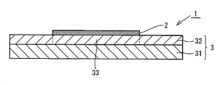
도 1은 본 실시 형태에 따른 다이싱 테이프 일체형 반도체 이면용 필름의 단면 모식도이다.
도 2는 박리 대전압의 측정 방법을 설명하기 위한 개략 구성도이다.
도 3은 다른 실시 형태에 따른 다이싱 테이프 일체형 반도체 이면용 필름의 단면 모식도이다.
도 4는 다른 실시 형태에 따른 다이싱 테이프 일체형 반도체 이면용 필름의 단면 모식도이다.
도 5는 본 실시 형태에 따른 다이싱 테이프 일체형 반도체 이면용 필름을 이용한 반도체 장치의 제조 방법의 일례를 나타내는 단면 모식도이다.BRIEF DESCRIPTION OF DRAWINGS FIG. 1 is a cross-sectional schematic diagram of a semiconductor backing film with a dicing tape integral type according to the present embodiment. FIG.
Fig. 2 is a schematic diagram for explaining a method of measuring the peeling electrification voltage.
3 is a cross-sectional schematic diagram of a dicing tape-integrated semiconductor backside film according to another embodiment.
4 is a cross-sectional schematic diagram of a dicing tape-integrated semiconductor backside film according to another embodiment.
5 is a schematic cross-sectional view showing an example of a method of manufacturing a semiconductor device using a dicing tape-integrated semiconductor backing film according to the present embodiment.
<제1 본 발명><First Invention>
제1 본 발명의 실시 형태에 대하여, 도면을 참조하면서 설명하지만, 제1 본 발명은 이들의 예에 한정되지 않는다. 이하에서는 우선, 제1 본 발명의 다이싱 테이프 일체형 접착 시트가 다이싱 테이프 일체형 반도체 이면용 필름인 경우에 대하여 설명한다. 즉, 제1 본 발명의 접착 시트가, 플립 칩형 반도체 이면용 필름인 경우에 대하여 설명한다. 도 1은, 본 실시 형태에 따른 다이싱 테이프 일체형 반도체 이면용 필름의 일례를 나타내는 단면 모식도이다. 또한, 본 명세서에 있어서, 도면에는, 설명에 불필요한 부분은 생략하고, 또한 설명을 용이하게 하기 위해 확대 또는 축소 등을 하여 도시한 부분이 있다.BEST MODE FOR CARRYING OUT THE INVENTION Embodiments of the first invention will be described with reference to the drawings, but the first invention is not limited to these examples. Hereinafter, the case where the dicing tape-integrated adhesive sheet of the first invention is a dicing tape-integrated semiconductor backside film will be described. That is, the case where the adhesive sheet of the first invention is a film for flip-chip type semiconductor backing will be described. 1 is a schematic cross-sectional view showing an example of a dicing tape-integrated semiconductor backing film according to the present embodiment. Also, in this specification, unnecessary portions are omitted in the drawings, and the drawings are enlarged or reduced in order to facilitate explanation.
(다이싱 테이프 일체형 반도체 이면용 필름)(Dicing Tape-integrated Semiconductor Backside Film)
도 1에서 도시된 바와 같이, 다이싱 테이프 일체형 반도체 이면용 필름(1)은, 기재(31) 위에 점착제층(32)이 형성된 다이싱 테이프(3)와, 점착제층(32) 위에 형성된 플립 칩형 반도체 이면용 필름(2: 이하, 「반도체 이면용 필름」이라 하는 경우가 있음)을 구비하는 구성이다. 또한, 제1 본 발명의 다이싱 테이프 일체형 반도체 이면용 필름은, 도 1에서 도시된 바와 같이, 다이싱 테이프(3)의 점착제층(32) 위에 있어서, 반도체 웨이퍼의 점착 부분에 대응하는 부분(33)에만 반도체 이면용 필름(2)이 형성된 구성이어도 되지만, 점착제층(32)의 전체면에 반도체 이면용 필름이 형성된 구성이어도 되고, 또한 반도체 웨이퍼의 점착 부분에 대응하는 부분(33)보다 크면서 점착제층(32)의 전체면보다 작은 부분에 반도체 이면용 필름이 형성된 구성이어도 된다. 또한, 반도체 이면용 필름(2)의 표면(웨이퍼의 이면에 점착되는 측의 표면)은 웨이퍼 이면에 점착될 때까지 동안, 세퍼레이터 등에 의해 보호되어 있어도 된다.1, the dicing tape-integrated
다이싱 테이프 일체형 반도체 이면용 필름(1)에 있어서, 박리 속도 10m/분, 박리 각도 150°에서의 박리 시험에 있어서의, 점착제층(32)과 접착 시트(2)의 박리력은, 0.02 내지 0.5N/20㎜이며, 바람직하게는 0.02 내지 0.3N/20㎜이며, 보다 바람직하게는 0.02 내지 0.2N/20㎜이다. 상기 박리력이 0.02N/20㎜ 이상이기 때문에, 다이싱 시에는 반도체 웨이퍼를 고정할 수 있다. 또한, 상기 박리력이 0.5N/20㎜ 이하이기 때문에, 픽업 시에는, 용이하게 접착 시트(2)가 부착된 반도체 소자를, 점착제층(32)으로부터 박리할 수 있다.The peel strength of the pressure-
또한, 다이싱 테이프 일체형 반도체 이면용 필름(1)에 있어서, 상기 박리 시험에 의한 조건에 따라 점착제층(32)과 접착 시트(2)를 박리하였을 때의 박리 대전압의 절댓값은, 0.5㎸ 이하(-0.5㎸ 내지 +0.5㎸)이고, 바람직하게는 0.3㎸ 이하(-0.3㎸내지 +0.3㎸)이며, 보다 바람직하게는 0.2㎸ 이하(-0.2㎸ 내지 +0.2㎸)이다. 상기 박리 시험에 의한 조건에 따라 점착제층(32)과 접착 시트(2)를 박리하였을 때의 박리 대전압의 절댓값이 0.5㎸ 이하이기 때문에, 대전 방지 효과를 발휘할 수 있다. 그 결과, 픽업 시의 박리 대전에 의해 반도체 소자가 파괴되는 것을 방지하고, 디바이스로서의 신뢰성을 향상시키는 것이 가능해진다.Further, in the dicing tape-integrated semiconductor backside film (1), the maximum value of the peeling electrification voltage when the pressure-sensitive adhesive layer (32) and the adhesive sheet (2) are peeled off under the conditions of the peeling test is 0.5 kV or less (-0.5 kV to +0.5 kV), preferably 0.3 kV or less (-0.3 kV to +0.3 kV), and more preferably 0.2 kV or less (-0.2 kV to +0.2 kV). The total value of the peeling electrification voltage when peeling the pressure-
여기서, 박리 대전압의 측정 방법에 대하여 설명한다.Here, a method of measuring the peeling electrification voltage will be described.
도 2는, 박리 대전압의 측정 방법을 설명하기 위한 개략 구성도이다. 우선, 미리 제전해 둔 아크릴판(100)(두께: 1㎜, 폭: 70㎜, 길이: 100㎜)에, 다이싱 테이프 일체형 반도체 이면용 필름(1)을 접합한다. 접합에는, 핸드 롤러를 이용하고, 양면 테이프를 개재하여 아크릴판(100)과 다이싱 테이프(3)가 대향하도록 행한다. 이 상태에서, 23℃, 50% RH의 환경 하에서 하루 방치한다. 이어서, 샘플 고정대(102)에 다이싱 테이프 일체형 반도체 이면용 필름(1)을 접합한 아크릴판(100)을 고정한다. 이어서, 반도체 이면용 필름(2)의 단부를 자동 권취기에 고정하고, 박리 각도 150°, 박리 속도 10 m/min이 되도록 박리한다. 이때에 발생하는 다이싱 테이프(3)측의 면(점착제층(32)의 면)의 전위를, 다이싱 테이프의 표면으로부터 100㎜의 위치에 고정해 놓은 전위 측정기(104: 카스가덴키사 제조, KSD-0103)로 측정한다. 측정은, 23℃, 50% RH의 환경 하에서 행한다.Fig. 2 is a schematic structural view for explaining a method of measuring the peeling electrification voltage. First, a dicing tape-integrated
다이싱 테이프 일체형 반도체 이면용 필름(1)에 있어서, 기재(31), 점착제층(32), 또는 반도체 이면용 필름(2) 중 적어도 어느 하나의 표면에 있어서의 표면 고유 저항값은, 바람직하게는 1.0×10¹¹Ω 이하이고, 보다 바람직하게는 1.0×10¹⁰Ω 이하이며, 더 바람직하게는 1.0×10⁹Ω 이하이다. 또한, 상기 표면 고유 저항값은, 작을수록 바람직하지만, 예를 들어 1.0×10⁵Ω 이상, 1.0×10⁶Ω 이상, 1.0×10⁷Ω 이상을 들 수 있다. 상기 표면 고유 저항값이, 1.0×10¹¹Ω 이하이면, 대전하기 어렵다. 따라서, 대전 방지 효과를 보다 발휘할 수 있다. 또한, 제1 본 발명에 있어서, 기재, 점착제층, 또는 반도체 이면용 필름 중 적어도 어느 하나의 표면에 있어서의 표면 고유 저항값이란, 기재의 점착제층측의 표면, 기재의 점착제층과는 반대측의 표면, 점착제층의 기재측의 표면, 점착제층의 기재와는 반대측의 표면, 반도체 이면용 필름의 점착제층측의 표면, 반도체 이면용 필름의 점착제층과는 반대측의 표면 중 적어도 어느 하나의 표면에 있어서의 표면 고유 저항값을 말한다. 상기 표면 고유 저항값은, 실시예 기재의 방법에 의해 측정되는 값을 말한다.In the dicing tape-integrated semiconductor backing film (1), the surface resistivity of the surface of at least one of the substrate (31), the pressure sensitive adhesive layer (32), and the semiconductor backing film (2) Is not more than 1.0 x 10 11 ?, More preferably not more than 1.0 x 10 10 ?, And still more preferably not more than 1.0 x 10 9 ?. The surface resistivity value is preferably as small as possible, but may be, for example, 1.0 x 10 5 Ω or more, 1.0 × 10 6 Ω or more, or 1.0 × 10 7 Ω or more. If the surface resistivity is 1.0 x 10 < 11 > or less, it is difficult to charge. Therefore, the antistatic effect can be further exerted. In the first invention, the surface resistivity value of the surface of at least one of the substrate, the pressure-sensitive adhesive layer, and the film for backing the semiconductor means the surface of the substrate on the side of the pressure-sensitive adhesive layer, On the surface of the substrate side of the pressure-sensitive adhesive layer, the surface of the pressure-sensitive adhesive layer opposite to the substrate, the surface of the semiconductor backing film side of the pressure-sensitive adhesive layer side, and the surface of the semiconductor backside film opposite to the pressure- Surface resistivity value. The surface resistivity value refers to a value measured by the method described in Examples.
다이싱 테이프 일체형 반도체 이면용 필름(1)에 있어서, 기재(31), 점착제층(32), 반도체 이면용 필름(2) 중 적어도 하나에는, 대전 방지제가 함유되어 있는 것이 바람직하다.It is preferable that an antistatic agent is contained in at least one of the
기재(31)에 대전 방지제가 함유되어 있으면, 다이싱 테이프(3)를 고정하는 흡착대로부터 제거할 때의, 기재(31)와 흡착대 사이에서의 박리 대전을 억제할 수 있다. 특히, 기재(31)가 다층 구조를 갖고 있으며, 다층 구조의 기재(31)의 점착제층(32)측의 최외층에 대전 방지제가 함유되어 있으면, 기재(31)와 점착제층(32)의 양쪽 대전을 억제할 수 있다. 또한, 다층 구조의 기재(31)의 점착제층(32)과는 반대측의 최외층에 대전 방지제가 함유되어 있으면, 기재(31)와 흡착대 사이의 박리 대전을 더 효과적으로 억제할 수 있다.When the antistatic agent is contained in the
또한, 점착제층(32)에 대전 방지제가 함유되어 있으면, 점착제층(32)과 반도체 이면용 필름(2)을 박리하였을 때의 박리 대전을 더 효과적으로 억제할 수 있다.Further, if the pressure sensitive
또한, 반도체 이면용 필름(2)에 대전 방지제가 함유되어 있으면, 다이싱 테이프(3)로부터 박리한 후에도 대전 방지 효과를 갖는다. 그 결과, 다이싱 테이프(3)로부터 박리한 후에도, 대전에 의한 반도체 소자의 파괴를 억제할 수 있다. 특히, 반도체 이면용 필름(2)이 다층 구조를 갖고 있으며, 다층 구조의 반도체 이면용 필름(2)에 있어서의 다이싱 테이프(3)측의 최외층에 대전 방지제가 함유되어 있으면, 점착제층(32)과 반도체 이면용 필름(2)을 박리하였을 때의 박리 대전을 더 효과적으로 억제할 수 있다.Further, if the
상기 대전 방지제로서는, 제4급 암모늄염, 피리디늄염, 제1, 제2, 제3 아미노기 등의 양이온성 관능기를 갖는 양이온형 대전 방지제, 술폰산염이나 황산 에스테르염, 포스폰산염, 인산 에스테르염 등의 음이온성 관능기를 갖는 음이온형 대전 방지제, 알킬베타인 및 그의 유도체, 이미다졸린 및 그의 유도체, 알라닌 및 그의 유도체 등의 양성형 대전 방지제, 아미노알코올 및 그의 유도체, 글리세린 및 그의 유도체, 폴리에틸렌글리콜 및 그의 유도체 등의 비이온형 대전 방지제, 나아가, 상기 양이온형, 음이온형, 양성 이온형의 이온 도전성기를 갖는 단량체를 중합 또는 공중합하여 얻어진 이온 도전성 중합체(고분자형 대전 방지제)를 들 수 있다. 이들 화합물은 단독으로 사용해도 되고, 또한 2종 이상을 혼합하여 사용해도 된다. 그 중에서도, 고분자형 대전 방지제가 바람직하다. 고분자형 대전 방지제를 이용하면, 기재(31), 점착제층(32) 및 반도체 이면용 필름(2)으로부터 블리드하기 어렵다. 그 결과, 경시에 의한 대전 방지 기능의 저하를 억제할 수 있다.Examples of the antistatic agent include cationic antistatic agents having cationic functional groups such as quaternary ammonium salts, pyridinium salts, primary, secondary and tertiary amino groups, sulfonic acid salts and sulfuric acid ester salts, phosphonic acid salts and phosphoric acid ester salts An antioxidant type antistatic agent having an anionic functional group, alkylbetaines and derivatives thereof, amphoteric antistatic agents such as imidazolines and derivatives thereof, alanines and derivatives thereof, aminoalcohols and derivatives thereof, glycerin and derivatives thereof, polyethylene glycols and (Ionic conductive antistatic agent) obtained by polymerizing or copolymerizing a monomer having an ion-conductive group of the cationic, anionic, or positive ion type. These compounds may be used alone or in combination of two or more. Among them, a polymer type antistatic agent is preferable. It is difficult to bleed from the
구체적으로는, 양이온형 대전 방지제로서, 예를 들어 알킬트리메틸암모늄 염, 아실로일아미드프로필트리메틸암모늄 메토술페이트, 알킬벤질메틸암모늄염, 아실염화콜린, 폴리디메틸아미노에틸메타크릴레이트 등의 4급 암모늄기를 갖는 (메트)아크릴레이트 공중합체, 폴리비닐벤질트리메틸암모늄 클로라이드 등의 4급 암모늄기를 갖는 스티렌 공중합체, 폴리디알릴디메틸암모늄 클로라이드 등의 4급 암모늄기를 갖는 디알릴아민 공중합체 등을 들 수 있다. 이들 화합물은 단독으로 사용해도 되고, 또한 2종 이상을 혼합하여 사용해도 된다.Specifically, examples of the cationic antistatic agent include quaternary ammonium groups such as alkyltrimethylammonium salts, acyloylamidopropyltrimethylammonium methosulfate, alkylbenzylmethylammonium salts, acyl chloride choline, polydimethylaminoethyl methacrylate and the like , Styrene copolymers having quaternary ammonium groups such as polyvinylbenzyltrimethylammonium chloride, and diallylamine copolymers having quaternary ammonium groups such as polydiallyldimethylammonium chloride, and the like . These compounds may be used alone or in combination of two or more.
음이온형 대전 방지제로서, 예를 들어 알킬술폰산염, 알킬벤젠술폰산염, 알킬황산에스테르염, 알킬에톡시황산에스테르염, 알킬인산에스테르염, 술폰산기 함유 스티렌 공중합체를 들 수 있다. 이들 화합물은 단독으로 사용해도 되고, 또한 2종 이상을 혼합하여 사용해도 된다.Examples of the anion-type antistatic agent include alkylsulfonic acid salts, alkylbenzenesulfonic acid salts, alkylsulfuric acid ester salts, alkyl ethoxy sulfuric acid ester salts, alkyl phosphoric acid ester salts and sulfonic acid group-containing styrene copolymers. These compounds may be used alone or in combination of two or more.
양성 이온형 대전 방지제로서, 예를 들어 알킬베타인, 알킬이미다졸륨베타인, 카르보베타인 그래프트 공중합을 들 수 있다. 이들 화합물은 단독으로 사용해도 되고, 또한 2종 이상을 혼합하여 사용해도 된다.Examples of positive ion-type antistatic agents include alkyl betaine, alkyl imidazolium betaine, and carbobetaine graft copolymer. These compounds may be used alone or in combination of two or more.
비이온형 대전 방지제로서, 예를 들어 지방산 알킬롤아미드, 디(2-히드록시에틸)알킬아민, 폴리옥시에틸렌알킬아민, 지방산 글리세린 에스테르, 폴리옥시에틸렌글리콜 지방산 에스테르, 소르비탄 지방산 에스테르, 폴리옥시 소르비탄 지방산 에스테르, 폴리옥시에틸렌알킬페닐에테르, 폴리옥시에틸렌알킬에테르, 폴리에틸렌글리콜, 폴리옥시에틸렌디아민, 폴리에테르와 폴리에스테르와 폴리아미드를 포함하여 이루어지는 공중합체, 메톡시폴리에틸렌글리콜 (메트)아크릴레이트 등을 들 수 있다. 이들 화합물은 단독으로 사용해도 되고, 또한 2종 이상을 혼합하여 사용해도 된다.Examples of the nonionic antistatic agent include fatty acid alkylol amide, di (2-hydroxyethyl) alkylamine, polyoxyethylene alkylamine, fatty acid glycerin ester, polyoxyethylene glycol fatty acid ester, sorbitan fatty acid ester, Sorbitan fatty acid esters, polyoxyethylene alkyl phenyl ethers, polyoxyethylene alkyl ethers, polyethylene glycols, polyoxyethylenediamines, polyethers, copolymers comprising polyesters and polyamides, methoxypolyethylene glycol (meth) acrylates And the like. These compounds may be used alone or in combination of two or more.
고분자형 대전 방지제의 다른 예로서는, 예를 들어 폴리아닐린, 폴리피롤, 폴리티오펜 등을 들 수 있다.Other examples of the polymer type antistatic agent include, for example, polyaniline, polypyrrole, and polythiophene.
또한, 상기 대전 방지제로서, 도전성 물질을 들 수 있다. 도전성 물질로서는, 예를 들어 산화주석, 산화안티몬, 산화인듐, 산화카드뮴, 산화티타늄, 산화아연, 인듐, 주석, 안티몬, 금, 은, 구리, 알루미늄, 니켈, 크롬, 티타늄, 철, 코발트, 요오드화 구리 및 그 합금 또는 혼합물을 들 수 있다.As the antistatic agent, a conductive material can be mentioned. Examples of the conductive material include tin oxide, antimony oxide, indium oxide, cadmium oxide, titanium oxide, zinc oxide, indium, tin, antimony, gold, silver, copper, aluminum, nickel, chromium, titanium, iron, cobalt, Copper and alloys or mixtures thereof.
상기 대전 방지제의 함유량은, 첨가하는 층의 수지 성분 전체에 대하여 50중량% 이하인 것이 바람직하고, 30중량% 이하인 것이 보다 바람직하다. 또한, 상기 대전 방지제의 함유량은, 첨가하는 층의 수지 성분 전체에 대하여 5중량% 이상인 것이 바람직하고, 10중량% 이상인 것이 보다 바람직하다. 상기 대전 방지제를 상기 수치 범위 내에서 함유시킴으로써, 첨가하는 층의 기능을 해하지 않고 대전 방지 기능을 부가할 수 있다. 여기서, 「첨가하는 층의 수지 성분 전체에 대하여 50중량% 이하」란, 이하를 의미한다.The content of the antistatic agent is preferably 50% by weight or less, more preferably 30% by weight or less based on the total resin component of the layer to be added. The content of the antistatic agent is preferably 5% by weight or more, more preferably 10% by weight or more, based on the total resin component of the layer to be added. By incorporating the antistatic agent within the above-described numerical range, the antistatic function can be added without deteriorating the function of the layer to be added. Here, " 50% by weight or less based on the total resin component of the layer to be added " means the following.
(a) 첨가하는 층이 기재(31)인 경우(a) When the layer to be added is the
기재(31)가 1층을 포함하여 이루어지는 경우에는, 기재(31)를 구성하는 수지 성분 전체에 대하여 50중량% 이하를 의미한다.In the case where the
기재(31)가 다층 구조를 포함하여 이루어지는 경우에는, 복수의 층 중 하나의 층을 구성하는 수지 성분 전체에 대하여 50중량% 이하를 의미한다.In the case where the
(b) 첨가하는 층이 점착제층(32)인 경우(b) When the layer to be added is the pressure-
점착제층(32)을 구성하는 수지 성분 전체에 대하여 50중량% 이하를 의미한다.Means that the total amount of the resin components constituting the pressure-
(c) 첨가하는 층이 반도체 이면용 필름(2)인 경우(c) When the layer to be added is the semiconductor backing film (2)
반도체 이면용 필름(2)이 1층을 포함하여 이루어지는 경우에는, 반도체 이면용 필름(2)을 구성하는 수지 성분 전체에 대하여 50중량% 이하를 의미한다.In the case where the
반도체 이면용 필름(2)이 다층 구조를 포함하여 이루어지는 경우에는, 복수의 층 중 하나의 층을 구성하는 수지 성분 전체에 대하여 50중량% 이하를 의미한다.When the
또한, 「첨가하는 층의 수지 성분 전체에 대하여 30중량% 이하」, 「첨가하는 층의 수지 성분 전체에 대하여 5중량% 이상」, 「첨가하는 층의 수지 성분 전체에 대하여 10중량% 이상」에 관해서도, 상기와 마찬가지로, 기재, 점착제층, 반도체 이면용 필름이 1층을 포함하여 이루어지는 경우에는, 상기 기재, 상기 점착제층, 또는 상기 반도체 이면용 필름을 구성하는 수지 성분 전체에 대한 비율을 말하고, 다층 구조를 포함하여 이루어지는 경우에는, 상기 기재, 또는 상기 반도체 이면용 필름을 구성하는 복수의 층 중 하나의 층을 구성하는 수지 성분 전체에 대한 비율을 의미한다.Further, "not more than 30 wt% of all the resin components of the layer to be added", "not less than 5 wt% of all the resin components of the layer to be added", "not less than 10 wt% of the total resin components of the layer to be added" In the case where the substrate, the pressure-sensitive adhesive layer, and the semiconductor backing film include one layer as well as the above, the ratio of the total amount of the resin components constituting the base material, the pressure-sensitive adhesive layer, In the case of including a multilayer structure, it means the ratio of the resin component constituting one of the plurality of layers constituting the base material or the back surface film.
다이싱 테이프 일체형 반도체 이면용 필름에 있어서는, 기재 중 적어도 한쪽의 면 위에, 대전 방지제를 함유하는 대전 방지제층이 형성되어 있어도 된다. 도 3 및 도 4는, 다른 실시 형태에 따른 다이싱 테이프 일체형 반도체 이면용 필름의 단면 모식도이다.In the dicing tape-integrated semiconductor backing film, an antistatic agent layer containing an antistatic agent may be formed on at least one surface of the substrate. Figs. 3 and 4 are sectional schematic views of a dicing tape-integrated semiconductor backside film according to another embodiment. Fig.
도 3에 도시한 바와 같이, 다이싱 테이프 일체형 반도체 이면용 필름(10)은, 기재(31) 위에 점착제층(32)이 형성된 다이싱 테이프(3)와, 점착제층(32) 위에 형성된 반도체 이면용 필름(2)과, 기재(31)의 점착제층(32)과는 반대측의 면 위에 대전 방지제층(35)이 형성되어 있다. 다이싱 테이프 일체형 반도체 이면용 필름(10)에서는, 기재(31)의 점착제층(32)과는 반대측의 면 위에 대전 방지제층(35)이 형성되어 있기 때문에, 기재(31)와 흡착대 사이의 박리 대전을 보다 효과적으로 억제할 수 있다.3, the dicing tape-integrated
또한, 도 4에 도시한 바와 같이, 다이싱 테이프 일체형 반도체 이면용 필름(20)은, 기재(31) 위에 점착제층(32)이 형성된 다이싱 테이프(3)와, 기재(31)와 점착제층(32)의 사이에 형성된 대전 방지제층(36)과, 점착제층(32) 위에 형성된 반도체 이면용 필름(2)을 구비하는 구성이다. 다이싱 테이프 일체형 반도체 이면용 필름(20)에서는, 기재(31)의 점착제층(32)측의 면 위에, 대전 방지제층(36)이 형성되어 있기 때문에, 기재(31)와 점착제층(32)의 양쪽 대전을 억제할 수 있다.4, the dicing tape integral
(대전 방지제층)(Antistatic agent layer)
대전 방지제층(35, 36)은 적어도 대전 방지제를 함유하는 층이다. 대전 방지제층(35, 36)에 함유시키는 대전 방지제로서는, 기재(31), 점착제층(32), 반도체 이면용 필름(2)에 함유시키는 경우의 상기 대전 방지제와 마찬가지의 것을 사용할 수 있다. 또한, 대전 방지제층(35, 36)에는, 대전 방지제 이외에 필요에 따라서, 바인더 성분, 용제 등을 함유시켜도 된다.The antistatic agent layers 35 and 36 are layers containing at least an antistatic agent. The antistatic agent contained in the antistatic agent layers 35 and 36 may be the same antistatic agent as the antistatic agent contained in the
대전 방지제층(35, 36)의 두께는, 바람직하게는 0.01 내지 5㎛이며, 보다 바람직하게는 0.03 내지 1㎛이다. 대전 방지제층(35), 대전 방지제층(36)의 두께를 0.01㎛ 이상으로 함으로써, 대전 방지 기능을 발현하기 쉽게 할 수 있다. 또한, 대전 방지제층(35), 대전 방지제층(36)의 두께를 5㎛ 이하로 함으로써, 점착제와 기재의 밀착 성능을 향상시킬 수 있다.The thickness of the antistatic agent layers 35 and 36 is preferably 0.01 to 5 占 퐉, and more preferably 0.03 to 1 占 퐉. By making the thickness of the
대전 방지제층(35, 36)은, 대전 방지제층 형성용 용액을 기재(31)에 도포하고, 건조시킴으로써 형성할 수 있다. 도포 방법으로서는, 스핀 코트, 스프레이 코트, 딥 코트, 스크린 인쇄, 와이어 바 코트 등의 각종 도포 방법을 채용할 수 있다.The antistatic agent layers 35 and 36 can be formed by applying a solution for forming an antistatic agent layer to the
(플립 칩형 반도체 이면용 필름)(Flip chip type semiconductor backing film)
반도체 이면용 필름(2)은 필름 형상의 형태를 갖고 있다. 반도체 이면용 필름(2)은, 통상적으로 제품으로서의 다이싱 테이프 일체형 반도체 이면용 필름의 형태에서는, 미경화 상태(반경화 상태를 포함함)이며, 다이싱 테이프 일체형 반도체 이면용 필름을 반도체 웨이퍼에 점착시킨 후에 열경화된다(상세에 대해서는 후술함).The
상기 반도체 이면용 필름은, 수지 조성물에 의해 형성할 수 있고, 열가소성 수지와 열경화성 수지를 포함하는 수지 조성물에 의해 구성할 수 있다. 또한, 반도체 이면용 필름은, 열경화성 수지가 이용되고 있지 않은 열가소성 수지 조성물로 구성되어 있어도 되고, 열가소성 수지가 이용되고 있지 않은 열경화성 수지 조성물로 구성되어 있어도 된다.The film for backside of semiconductor can be formed from a resin composition and can be composed of a resin composition comprising a thermoplastic resin and a thermosetting resin. Further, the film for backside of semiconductor may be composed of a thermoplastic resin composition not using a thermosetting resin, or may be composed of a thermosetting resin composition not using a thermoplastic resin.
상기 열가소성 수지로서는, 예를 들어 천연 고무, 부틸 고무, 이소프렌 고무, 클로로프렌 고무, 에틸렌-아세트산 비닐 공중합체, 에틸렌-아크릴산 공중합체, 에틸렌-아크릴산 에스테르 공중합체, 폴리부타디엔 수지, 폴리카르보네이트 수지, 열가소성 폴리이미드 수지, 6-나일론이나 6,6-나일론 등의 폴리아미드 수지, 페녹시 수지, 아크릴 수지, PET(폴리에틸렌테레프탈레이트)나 PBT(폴리부틸렌테레프탈레이트) 등의 포화 폴리에스테르 수지, 폴리아미드이미드 수지, 또는 불소 수지 등을 들 수 있다. 열가소성 수지는 단독으로 또는 2종 이상을 병용하여 이용할 수 있다. 이들 열가소성 수지 중에서도 아크릴 수지나 페녹시 수지가 적합하며, 나아가, 인장 저장 탄성률을 높게 유지하면서, 필름화하는 것이 가능한 페녹시 수지가 특히 바람직하다.Examples of the thermoplastic resin include natural rubber, butyl rubber, isoprene rubber, chloroprene rubber, ethylene-vinyl acetate copolymer, ethylene-acrylic acid copolymer, ethylene-acrylic acid ester copolymer, polybutadiene resin, polycarbonate resin, A thermoplastic polyimide resin, a polyamide resin such as 6-nylon or 6,6-nylon, a phenoxy resin, an acrylic resin, a saturated polyester resin such as PET (polyethylene terephthalate) or PBT (polybutylene terephthalate) Amide imide resins, fluorine resins and the like. The thermoplastic resins may be used alone or in combination of two or more. Of these thermoplastic resins, acrylic resins and phenoxy resins are suitable, and furthermore, phenoxy resins capable of forming a film while maintaining a high tensile storage elastic modulus are particularly preferable.
상기 페녹시 수지로서는, 특별히 한정되는 것이 아니라, 예를 들어 에피클로로히드린과 2가의 페놀계 화합물의 반응에 의해 얻어지는 수지나, 2가의 에폭시계 화합물과 2가의 페놀계 화합물의 반응에 의해 얻어지는 수지 등의 페놀 성분이 구성 단위로 들어 있는 에폭시 수지 등을 들 수 있다. 페녹시 수지로서는, 예를 들어 비스페놀 골격(비스페놀 A형 골격, 비스페놀 F형 골격, 비스페놀 A/F 혼합형 골격, 비스페놀 S형 골격, 비스페놀 M형 골격, 비스페놀 P형 골격, 비스페놀 A/P 혼합형 골격, 비스페놀 Z형 골격 등), 나프탈렌 골격, 노르보르넨 골격, 플루오렌 골격, 비페닐 골격, 안트라센 골격, 노볼락 골격, 피렌 골격, 크산틴 골격, 아다만탄 골격 및 디시클로펜타디엔 골격으로부터 선택된 적어도 하나의 골격을 갖는 페녹시 수지 등이 예시된다. 또한, 페녹시 수지는 시판품을 이용할 수도 있다. 페녹시 수지는 단독으로 또는 2종 이상을 조합하여 이용할 수 있다.The phenoxy resin is not particularly limited, and examples thereof include a resin obtained by reaction of epichlorohydrin and a divalent phenol compound, a resin obtained by a reaction between a divalent epoxy compound and a divalent phenol compound And epoxy resin containing a phenol component as a constituent unit. Examples of the phenoxy resin include bisphenol skeleton (bisphenol A skeleton, bisphenol F skeleton, bisphenol A / F mixed skeleton, bisphenol S skeleton, bisphenol M skeleton, bisphenol P skeleton, bisphenol A / P mixed skeleton, Bisphenol Z skeleton, etc.), a naphthalene skeleton, a norbornene skeleton, a fluorene skeleton, a biphenyl skeleton, an anthracene skeleton, a novolac skeleton, a pyrene skeleton, a xanthan skeleton, an adamantane skeleton, and a dicyclopentadiene skeleton And phenoxy resins having one skeleton. A commercially available phenoxy resin may also be used. The phenoxy resins may be used alone or in combination of two or more.
상기 아크릴 수지로서는, 특별히 한정되는 것이 아니라, 탄소수 30 이하(바람직하게는 탄소수 4 내지 18, 더 바람직하게는 탄소수 6 내지 10, 특히 바람직하게는 탄소수 8 또는 9)의 직쇄 또는 분지의 알킬기를 갖는 아크릴산 또는 메타크릴산의 에스테르의 1종 또는 2종 이상을 성분으로 하는 중합체 등을 들 수 있다. 즉, 제1 본 발명에서는, 아크릴 수지란, 메타크릴 수지도 포함하는 광의의 의미이다. 상기 알킬기로서는, 예를 들어 메틸기, 에틸기, 프로필기, 이소프로필기, n-부틸기, t-부틸기, 이소부틸기, 펜틸기, 이소펜틸기, 헥실기, 헵틸기, 2-에틸헥실기, 옥틸기, 이소옥틸기, 노닐기, 이소노닐기, 데실기, 이소데실기, 운데실기, 도데실기(라우릴기), 트리데실기, 테트라데실기, 스테아릴기, 옥타데실기 등을 들 수 있다.The acrylic resin is not particularly limited and acrylic resin having a linear or branched alkyl group having 30 or less carbon atoms (preferably 4 to 18 carbon atoms, more preferably 6 to 10 carbon atoms, and particularly preferably 8 or 9 carbon atoms) Or a polymer composed of one or two or more kinds of esters of methacrylic acid. That is, in the first aspect of the present invention, the term "acrylic resin" means broad meaning including methacrylic resin. Examples of the alkyl group include a methyl group, an ethyl group, a propyl group, an isopropyl group, an n-butyl group, a t-butyl group, an isobutyl group, a pentyl group, an isopentyl group, a hexyl group, (Lauryl group), a tridecyl group, a tetradecyl group, a stearyl group, an octadecyl group, and the like may be optionally substituted with one or more substituents selected from the group consisting of an alkyl group, an alkenyl group, an alkynyl group, .
또한, 상기 아크릴 수지를 형성하기 위한 다른 단량체(알킬기의 탄소수가 30 이하의 아크릴산 또는 메타크릴산의 알킬에스테르 이외의 단량체)로서는, 특별히 한정되는 것이 아니라, 예를 들어 아크릴산, 메타크릴산, 카르복시에틸아크릴레이트, 카르복시펜틸아크릴레이트, 이타콘산, 말레산, 푸마르산 또는 크로톤산 등과 같은 카르복실기 함유 단량체, 무수 말레산 또는 무수 이타콘산 등과 같은 산무수물 단량체, (메트)아크릴산 2-히드록시에틸, (메트)아크릴산 2-히드록시프로필, (메트)아크릴산 4-히드록시부틸, (메트)아크릴산 6-히드록시헥실, (메트)아크릴산 8-히드록시옥틸, (메트)아크릴산 10-히드록시데실, (메트)아크릴산 12-히드록시라우릴 또는 (4-히드록시메틸시클로헥실)-메틸아크릴레이트 등과 같은 히드록실기 함유 단량체, 스티렌술폰산, 알릴술폰산, 2-(메트)아크릴아미드-2-메틸프로판술폰산, (메트)아크릴아미드프로판술폰산, 술포프로필(메트)아크릴레이트 또는 (메트)아크릴로일옥시나프탈렌술폰산 등과 같은 술폰산기 함유 단량체, 또는 2-히드록시에틸아크릴로일포스페이트 등과 같은 인산기 함유 단량체 등을 들 수 있다. 또한, (메트)아크릴산이란 아크릴산 및/또는 메타크릴산을 말하고, 제1 본 발명의 (메트)란 모두 마찬가지의 의미이다.The other monomers for forming the acrylic resin (monomers other than acrylic acid or alkyl ester of methacrylic acid having 30 or less carbon atoms in the alkyl group) are not particularly limited and include, for example, acrylic acid, methacrylic acid, Acrylate, carboxypentyl acrylate, itaconic acid, maleic acid, fumaric acid or crotonic acid, acid anhydride monomers such as maleic anhydride or itaconic anhydride, 2-hydroxyethyl (meth) (Meth) acrylate, 2-hydroxypropyl (meth) acrylate, 4-hydroxybutyl (meth) acrylate, 6-hydroxyhexyl Hydroxyl group-containing monomers such as 12-hydroxylauryl acrylate or (4-hydroxymethylcyclohexyl) -methylacrylate, styrene sulfonic acid, Sulfonic acid group-containing monomers such as sulfonic acid, 2- (meth) acrylamide-2-methylpropanesulfonic acid, (meth) acrylamidopropanesulfonic acid, sulfopropyl (meth) acrylate or (meth) acryloyloxynaphthalenesulfonic acid, - phosphoric acid group-containing monomers such as hydroxyethyl acryloyl phosphate and the like. Further, (meth) acrylic acid refers to acrylic acid and / or methacrylic acid, and (meth) in the first invention means the same meaning.
또한, 상기 열경화성 수지로서는, 에폭시 수지, 페놀 수지 외에, 아미노 수지, 불포화 폴리에스테르 수지, 폴리우레탄 수지, 실리콘 수지, 열경화성 폴리이미드 수지 등을 들 수 있다. 열경화성 수지는, 단독으로 또는 2종 이상 병용하여 사용할 수 있다. 열경화성 수지로서는, 특히 반도체 소자를 부식시키는 이온성 불순물 등 함유가 적은 에폭시 수지가 적합하다. 또한, 에폭시 수지의 경화제로서는 페놀 수지를 적합하게 이용할 수 있다.Examples of the thermosetting resin include an amino resin, an unsaturated polyester resin, a polyurethane resin, a silicone resin and a thermosetting polyimide resin in addition to an epoxy resin and a phenol resin. The thermosetting resins may be used alone or in combination of two or more. As the thermosetting resin, an epoxy resin having a small content of ionic impurities, which corrodes semiconductor elements in particular, is suitable. As the curing agent of the epoxy resin, a phenol resin can be suitably used.
에폭시 수지로서는, 특별히 한정은 없으며, 예를 들어 비스페놀 A형 에폭시 수지, 비스페놀 F형 에폭시 수지, 비스페놀 S형 에폭시 수지, 브롬화 비스페놀 A형 에폭시 수지, 수소 첨가 비스페놀 A형 에폭시 수지, 비스페놀 AF형 에폭시 수지, 비페닐형 에폭시 수지, 나프탈렌형 에폭시 수지, 플루오렌형 에폭시 수지, 페놀노볼락형 에폭시 수지, 오르토크레졸 노볼락형 에폭시 수지, 트리스히드록시페닐메탄형 에폭시 수지, 테트라페닐올에탄형 에폭시 수지 등의 2관능 에폭시 수지나 다관능 에폭시 수지, 또는 히단토인형 에폭시 수지, 트리스글리시딜이소시아누레이트형 에폭시 수지 또는 글리시딜아민형 에폭시 수지 등의 에폭시 수지를 이용할 수 있다.Examples of the epoxy resin include, but not limited to, bisphenol A type epoxy resin, bisphenol F type epoxy resin, bisphenol S type epoxy resin, brominated bisphenol A type epoxy resin, hydrogenated bisphenol A type epoxy resin, bisphenol AF type epoxy resin , Biphenyl type epoxy resin, naphthalene type epoxy resin, fluorene type epoxy resin, phenol novolak type epoxy resin, orthocresol novolak type epoxy resin, trishydroxyphenyl methane type epoxy resin, tetraphenylol ethane type epoxy resin, etc. Epoxy resin such as bifunctional epoxy resin, polyfunctional epoxy resin, hydantoin type epoxy resin, trisglycidyl isocyanurate type epoxy resin or glycidylamine type epoxy resin can be used.
에폭시 수지로서는, 상기 예시 중 노볼락형 에폭시 수지, 비페닐형 에폭시 수지, 트리스히드록시페닐메탄형 에폭시 수지, 테트라페닐올에탄형 에폭시 수지가 특히 바람직하다. 이들 에폭시 수지는, 경화제로서의 페놀 수지와의 반응성이 풍부하고, 내열성 등이 우수하기 때문이다.As the epoxy resin, novolak type epoxy resin, biphenyl type epoxy resin, trishydroxyphenylmethane type epoxy resin and tetraphenylol ethane type epoxy resin are particularly preferable among the above examples. These epoxy resins are rich in reactivity with a phenol resin as a curing agent and have excellent heat resistance.
또한, 상기 페놀 수지는, 상기 에폭시 수지의 경화제로서 작용하는 것으로, 예를 들어 페놀노볼락 수지, 페놀아르알킬 수지, 크레졸노볼락 수지, tert-부틸페놀노볼락 수지, 노닐페놀노볼락 수지 등의 노볼락형 페놀 수지, 레졸형 페놀 수지, 폴리파라옥시 스티렌 등의 폴리옥시 스티렌 등을 들 수 있다. 페놀 수지는 단독으로 또는 2종 이상을 병용하여 이용할 수 있다. 이들 페놀 수지 중 페놀노볼락 수지, 페놀아르알킬 수지가 특히 바람직하다. 반도체 장치의 접속 신뢰성을 향상시킬 수 있기 때문이다.The phenolic resin acts as a curing agent for the epoxy resin. Examples of the phenolic resin include phenol novolac resins, phenol aralkyl resins, cresol novolac resins, tert-butylphenol novolac resins and nonylphenol novolac resins. Novolak type phenol resins, resole type phenol resins, and polyoxystyrenes such as polyparaxyxystyrene. The phenol resin may be used alone or in combination of two or more. Of these phenolic resins, phenol novolac resins and phenol aralkyl resins are particularly preferable. This is because connection reliability of the semiconductor device can be improved.
에폭시 수지와 페놀 수지의 배합 비율은, 예를 들어 상기 에폭시 수지 성분 중의 에폭시기 1당량당 페놀 수지 중의 수산기가 0.5당량 내지 2.0당량이 되도록 배합하는 것이 적합하다. 보다 적합한 것은 0.8당량 내지 1.2당량이다. 즉, 양자의 배합 비율이 상기 범위를 벗어나면, 충분한 경화 반응이 진행되지 않아, 에폭시 수지 경화물의 특성이 열화되기 쉬워지기 때문이다.The mixing ratio of the epoxy resin to the phenol resin is preferably such that the hydroxyl group in the phenol resin is equivalent to 0.5 to 2.0 equivalents per equivalent of the epoxy group in the epoxy resin component. More suitable is from 0.8 equivalents to 1.2 equivalents. That is, if the mixing ratio of the two is out of the above range, sufficient curing reaction does not proceed and the properties of the epoxy resin cured product tend to deteriorate.
제1 본 발명에서는, 에폭시 수지와 페놀 수지의 열경화 촉진 촉매가 이용되고 있어도 된다. 열경화 촉진 촉매로서는, 특별히 제한되지 않고, 공지된 열경화 촉진 촉매 중에서 적절히 선택하여 이용할 수 있다. 열경화 촉진 촉매는 단독으로 또는 2종 이상을 조합하여 이용할 수 있다. 열경화 촉진 촉매로서는, 예를 들어 아민계 경화 촉진제, 인계 경화 촉진제, 이미다졸계 경화 촉진제, 붕소계 경화 촉진제, 인-붕소계 경화 촉진제 등을 이용할 수 있다.In the first aspect of the present invention, a catalyst for accelerating thermal curing of an epoxy resin and a phenolic resin may be used. The thermosetting-promoting catalyst is not particularly limited and may be suitably selected from known thermosetting-promoting catalysts. The thermosetting promoting catalyst may be used alone or in combination of two or more. As the thermal curing accelerating catalyst, for example, amine-based curing accelerators, phosphorus-based curing accelerators, imidazole-based curing accelerators, boron-based curing accelerators, phosphorus-based curing accelerators and the like can be used.
상기 아민계 경화 촉진제로서는 특별히 한정되지 않고, 예를 들어 모노에탄올아민 트리플루오로보레이트(스텔라케미파(주) 제조), 디시안디아미드(나카라이테스크(주) 제조) 등을 들 수 있다.The amine-based curing accelerator is not particularly limited and includes, for example, monoethanolamine trifluoro borate (manufactured by Stella Chemipa) and dicyandiamide (manufactured by Nacalai Tesque).
상기 인계 경화 촉진제로서는 특별히 한정되지 않고, 예를 들어 트리페닐포스핀, 트리부틸포스핀, 트리(p-메틸페닐)포스핀, 트리(노닐페닐)포스핀, 디페닐트릴포스핀 등의 트리오르가노포스핀, 테트라페닐포스포늄브로마이드(상품명; TPP-PB), 메틸트리페닐포스포늄(상품명; TPP-MB), 메틸트리페닐포스포늄클로라이드(상품명; TPP-MC), 메톡시메틸트리페닐포스포늄(상품명; TPP-MOC), 벤질트리페닐포스포늄클로라이드(상품명; TPP-ZC) 등을 들 수 있다(모두 혹코카가쿠(주) 제조). 또한, 상기 트리페닐 포스핀계 화합물로서는, 에폭시 수지에 대하여 실질적으로 비용해성을 나타내는 것인 것이 바람직하다. 에폭시 수지에 대하여 비용해성이면, 열경화가 과도하게 진행하는 것을 억제할 수 있다. 트리페닐포스핀 구조를 가지면서, 에폭시 수지에 대하여 실질적으로 비용해성을 나타내는 열경화 촉매로서는, 예를 들어 메틸트리페닐포스포늄(상품명; TPP-MB) 등을 예시할 수 있다. 또한, 상기 「비용해성」이란, 트리페닐포스핀계 화합물을 포함하여 이루어지는 열경화 촉매가 에폭시 수지를 포함하여 이루어지는 용매에 대하여 불용성인 것을 의미하고, 보다 상세하게는, 온도 10 내지 40℃의 범위에 있어서 10중량% 이상 용해하지 않는 것을 의미한다.The phosphorus hardening accelerator is not particularly limited and examples of the phosphorus hardening accelerator include triorganophosphorus such as triphenylphosphine, tributylphosphine, tri (p-methylphenyl) phosphine, tri (nonylphenyl) phosphine, (Trade name: TPP-MB), methyltriphenylphosphonium chloride (trade name: TPP-MC), methoxymethyltriphenylphosphonium (trade name: (Trade name: TPP-MOC), benzyltriphenylphosphonium chloride (trade name: TPP-ZC) and the like (all manufactured by Kokagaku Co., Ltd.). The triphenylphosphine-based compound is preferably one which exhibits substantially no decomposition to the epoxy resin. If the epoxy resin is insoluble, it is possible to suppress the excessive progress of the thermosetting. As a thermosetting catalyst having a triphenylphosphine structure and exhibiting substantially no solubility in an epoxy resin, for example, methyltriphenylphosphonium (trade name: TPP-MB) can be exemplified. Means that the thermosetting catalyst comprising a triphenylphosphine-based compound is insoluble in a solvent containing an epoxy resin, and more specifically, it is in a temperature range of 10 to 40 ° C By weight and not more than 10% by weight.
상기 이미다졸계 경화 촉진제로서는, 2-메틸이미다졸(상품명; 2MZ), 2-운데실이미다졸(상품명; C11-Z), 2-헵타데실이미다졸(상품명; C17Z), 1,2-디메틸이미다졸(상품명; 1.2DMZ), 2-에틸-4-메틸이미다졸(상품명; 2E4MZ), 2-페닐이미다졸(상품명; 2PZ), 2-페닐-4-메틸이미다졸(상품명; 2P4MZ), 1-벤질-2-메틸이미다졸(상품명; 1B2MZ), 1-벤질-2-페닐이미다졸(상품명; 1B2PZ), 1-시아노에틸-2-메틸이미다졸(상품명; 2MZ-CN), 1-시아노에틸-2-운데실이미다졸(상품명; C11Z-CN), 1-시아노에틸-2-페닐이미다졸륨 트리멜리테이트(상품명; 2PZCNS-PW), 2,4-디아미노-6-[2'-메틸이미다졸릴-(1')]-에틸-s-트리아진(상품명; 2MZ-A), 2,4-디아미노-6-[2'-운데실이미다졸릴-(1')]-에틸-s-트리아진(상품명; C11Z-A), 2,4-디아미노-6-[2'-에틸-4'-메틸이미다졸릴-(1')]-에틸-s-트리아진(상품명; 2E4MZ-A), 2,4-디아미노-6-[2'-메틸이미다졸릴-(1')]-에틸-s-트리아진이소시아누르산 부가물(상품명; 2MA-OK), 2-페닐-4,5-디히드록시메틸이미다졸(상품명; 2PHZ-PW), 2-페닐-4-메틸-5-히드록시메틸이미다졸(상품명; 2P4MHZ-PW) 등을 들 수 있다(모두 시코쿠카세이코교(주) 제조).Examples of the imidazole-based curing accelerator include 2-methylimidazole (trade name: 2MZ), 2-undecylimidazole (trade name: C11-Z), 2-heptadecylimidazole Methylimidazole (trade name: 2E4MZ), 2-phenylimidazole (trade name: 2PZ), 2-phenyl-4-methylimidazole 2-methylimidazole (trade name: 1B2MZ), 1-benzyl-2-phenylimidazole (trade name: 1B2PZ), 1-cyanoethyl- (Product name: 2MZ-CN), 1-cyanoethyl-2-undecylimidazole (trade name: C11Z-CN), 1-cyanoethyl-2-phenylimidazolium trimellitate 2MZ-A), 2,4-diamino-6- (2'-methylimidazolyl- (2'-undecylimidazolyl- (1 ')] - ethyl-s-triazine (trade name: C11Z-A), 2,4-diamino- (1 ')] - ethyl-s-triazine (trade name: 2E4MZ-A), 2,4-diamino-6- [2'-methylimidazole 2-phenyl-4,5-dihydroxymethylimidazole (trade name: 2PHZ-PW), 2 (2'- -Phenyl-4-methyl-5-hydroxymethylimidazole (trade name: 2P4MHZ-PW) and the like (all manufactured by Shikoku Seiko KK).
상기 붕소계 경화 촉진제로서는 특별히 한정되지 않고, 예를 들어 트리클로로 보란 등을 들 수 있다.The boron-based curing accelerator is not particularly limited, and examples thereof include trichloroborane and the like.
상기 인-붕소계 경화 촉진제로서는 특별히 한정되지 않고, 예를 들어 테트라페닐포스포늄테트라페닐보레이트(상품명; TPP-K), 테트라페닐포스포늄테트라-p-트리보레이트(상품명; TPP-MK), 벤질트리페닐포스포늄테트라페닐보레이트(상품명; TPP-ZK), 트리페닐포스핀트리페닐보란(상품명; TPP-S) 등을 들 수 있다(모두 혹코카가쿠(주) 제조).The phosphorus-based curing accelerator is not particularly limited and includes, for example, tetraphenylphosphonium tetraphenylborate (trade name: TPP-K), tetraphenylphosphonium tetra-p-triborate (trade name: TPP-MK) Triphenylphosphonium tetraphenylborate (trade name: TPP-ZK), triphenylphosphine triphenylborane (trade name: TPP-S) and the like (all available from Hokokakaku Co., Ltd.).
상기 열경화 촉진 촉매의 비율은, 열경화성 수지 전량에 대하여 0.01중량% 이상 20중량% 이하인 것이 바람직하다. 열경화 촉진 촉매의 상기 비율이 0.01중량% 이상이면 피착체 위에 플립 칩 접속시킨 반도체 소자가 박형이어도(예를 들어, 두께가 300㎛ 이하, 나아가 200㎛ 이하이어도), 그 휨을 유효하게 억제 또는 방지할 수 있다. 또한, 열경화 촉진 촉매의 상기 비율을 20중량% 이하로 함으로써, 반도체 이면용 필름의 수축량이 과대해지지 않고, 적당한 크기로 컨트롤할 수 있다. 열경화 촉진 촉매의 상기 비율의 하한값으로서는, 바람직하게는 0.03중량% 이상(보다 바람직하게는 중량 0.05중량% 이상)이다. 또한, 상한값으로서는, 바람직하게는 18중량% 이하(보다 바람직하게는 15중량% 이하)이다.The proportion of the thermosetting promoting catalyst is preferably 0.01 wt% or more and 20 wt% or less with respect to the total amount of the thermosetting resin. When the above-mentioned proportion of the thermosetting-promoting catalyst is 0.01 wt% or more, even if the semiconductor element flip-chip-connected on the adherend is thin (for example, the thickness is 300 탆 or less, or even 200 탆 or less) can do. By controlling the ratio of the thermosetting accelerating catalyst to 20 wt% or less, it is possible to control the shrinkage amount of the semiconductor backing film to an appropriate size without excessting the shrinkage amount. The lower limit of the above-mentioned ratio of the thermosetting accelerating catalyst is preferably 0.03% by weight or more (more preferably 0.05% by weight or more). The upper limit value is preferably 18% by weight or less (more preferably 15% by weight or less).
상기 반도체 이면용 필름으로서는, 에폭시 수지 및 페놀 수지를 포함하는 수지 조성물에 의해 형성되어 있는 것이 바람직하고, 특히 에폭시 수지, 페놀 수지 및 페녹시 수지를 포함하는 수지 조성물에 의해 형성되어 있는 것이 적합하다.The semiconductor backing film is preferably formed of a resin composition containing an epoxy resin and a phenol resin, and more preferably formed of a resin composition comprising an epoxy resin, a phenol resin, and a phenoxy resin.
반도체 이면용 필름(2)은, 반도체 웨이퍼의 이면(회로 비형성면)에 대하여 접착성(밀착성)을 갖고 있는 것이 중요하다. 반도체 이면용 필름(2)은, 예를 들어 열경화성 수지로서의 에폭시 수지를 포함하는 수지 조성물에 의해 형성할 수 있다. 반도체 이면용 필름(2)을 미리 어느 정도 가교시켜 두기 위해서, 제작 시에, 중합체의 분자쇄 말단의 관능기 등과 반응하는 다관능성 화합물을 가교제로서 첨가시켜 두는 것이 바람직하다. 이에 의해, 고온 하에서의 접착 특성을 향상시켜, 내열성의 개선을 도모할 수 있다.It is important that the
반도체 이면용 필름의 반도체 웨이퍼에 대한 접착력(23℃, 박리 각도 180°, 박리 속도 300㎜/분)은 1N/10㎜ 폭 이상(예를 들어, 1N/10㎜ 폭 내지 10N/10㎜ 폭)인 것이 바람직하고, 더 바람직하게는 2N/10㎜ 폭 이상(예를 들어, 2N/10㎜ 폭 내지 10N/10㎜ 폭)이며, 특히 바람직하게는 4N/10㎜ 폭 이상(예를 들어, 4N/10㎜ 폭 내지 10N/10㎜ 폭 이상)으로 함으로써, 우수한 밀착성으로 반도체 웨이퍼나 반도체 소자에 접착되어 있어, 들뜸 등의 발생을 방지할 수 있다. 또한, 반도체 웨이퍼의 다이싱 시에 칩 탈락이 발생하는 것을 방지할 수도 있다. 또한, 반도체 이면용 필름의 반도체 웨이퍼에 대한 상기 접착력은, 예를 들어 다음과 같이 하여 측정한 값이다. 즉, 반도체 이면용 필름의 한쪽 면에, 점착 테이프(상품명 「BT315」닛토덴코(주) 제조)를 점착하여 이면 보강한다. 그 후, 이면 보강한 길이 150㎜, 폭 10㎜의 반도체 이면용 필름의 표면에, 두께 0.6㎜의 반도체 웨이퍼를, 50℃에서 2kg의 롤러를 1 왕복하여 열 라미네이트법에 의해 접합한다. 그 후, 열판 위(50℃)에 2분간 정치한 후, 상온(23℃ 정도)에서 20분 정치한다. 정치 후, 박리 시험기(상품명 「오토그래프 AGS-J」시마즈세이사쿠쇼사 제조)를 이용하여, 온도 23℃ 하에서, 박리 각도: 180°, 인장 속도: 300㎜/min의 조건 하에서, 이면 보강된 반도체 이면용 필름을 박리한다. 상기 접착력은, 이때의 반도체 이면용 필름과 반도체 웨이퍼의 계면에서 박리시켜 측정된 값(N/10㎜ 폭)이다.(For example, 1 N / 10 mm width to 10 N / 10 mm width) of the semiconductor backing film with respect to the semiconductor wafer (23 캜, peeling angle of 180 占 and peeling speed of 300 mm / min) (For example, 2N / 10 mm wide to 10 N / 10 mm wide), more preferably 4 N / 10 mm wide or more (for example, 4 N / 10 mm width to 10 N / 10 mm width or more), it is adhered to the semiconductor wafer or the semiconductor element with excellent adhesiveness, and the occurrence of lifting or the like can be prevented. In addition, it is also possible to prevent chips from falling off during dicing of the semiconductor wafer. The adhesive strength of the semiconductor backing film to the semiconductor wafer is, for example, a value measured in the following manner. That is, an adhesive tape (trade name "BT315" manufactured by Nitto Denko Corporation) is adhered to one side of the film for backside of the semiconductor to reinforce the backside. Thereafter, a semiconductor wafer having a thickness of 0.6 mm and a roller of 2 kg at a temperature of 50 占 폚 are reciprocated on the surface of the semiconductor backing film having a length of 150 mm and a width of 10 mm reinforced on the back side by heat lamination. Thereafter, the mixture is allowed to stand on a hot plate (50 DEG C) for 2 minutes, and then allowed to stand at room temperature (about 23 DEG C) for 20 minutes. After setting, under the condition of a peeling test machine (trade name "Autograph AGS-J" manufactured by Shimadzu Seisakusho) at a temperature of 23 ° C, a peel angle of 180 ° and a tensile rate of 300 mm / min, The backing film is peeled off. The adhesion is a value (N / 10 mm width) measured by peeling at the interface between the semiconductor backing film and the semiconductor wafer at this time.
상기 가교제로서는, 특별히 제한되지 않고, 공지된 가교제를 이용할 수 있다. 구체적으로는, 예를 들어 이소시아네이트계 가교제, 에폭시계 가교제, 멜라민계 가교제, 과산화물계 가교제 외에, 요소계 가교제, 금속 알콕시드계 가교제, 금속 킬레이트계 가교제, 금속염계 가교제, 카르보디이미드계 가교제, 옥사졸린계 가교제, 아지리딘계 가교제, 아민계 가교제 등을 들 수 있다. 가교제로서는, 이소시아네이트계 가교제나 에폭시계 가교제가 적합하다. 또한, 상기 가교제는 단독으로 또는 2종 이상 조합하여 사용할 수 있다.The crosslinking agent is not particularly limited, and a known crosslinking agent may be used. Specifically, in addition to an isocyanate crosslinking agent, an epoxy crosslinking agent, a melamine crosslinking agent, and a peroxide crosslinking agent, a urea crosslinking agent, a metal alkoxide crosslinking agent, a metal chelating crosslinking agent, a metal salt crosslinking agent, a carbodiimide crosslinking agent, Based crosslinking agents, aziridine-based crosslinking agents, and amine-based crosslinking agents. As the crosslinking agent, an isocyanate crosslinking agent and an epoxy crosslinking agent are suitable. The crosslinking agents may be used alone or in combination of two or more.
상기 이소시아네이트계 가교제로서는, 예를 들어 1,2-에틸렌디이소시아네이트, 1,4-부틸렌디이소시아네이트, 1,6-헥사메틸렌디이소시아네이트 등의 저급 지방족 폴리이소시아네이트류; 시클로펜틸렌디이소시아네이트, 시클로헥실렌디이소시아네이트, 이소포론디이소시아네이트, 수소 첨가 톨릴렌디이소시아네이트, 수소 첨가 크실렌디이소시아네이트 등의 지환족 폴리이소시아네이트류; 2,4-톨릴렌디이소시아네이트, 2,6-톨릴렌디이소시아네이트, 4,4'-디페닐메탄디이소시아네이트, 크실렌디이소시아네이트 등의 방향족 폴리이소시아네이트류 등을 들 수 있고, 그 밖에, 트리메틸올프로판/톨릴렌디이소시아네이트 삼량체 부가물[닛폰폴리우레탄코교(주) 제조, 상품명 「코로네이트 L」], 트리메틸올프로판/헥사메틸렌디이소시아네이트 삼량체 부가물[닛폰폴리우레탄코교(주) 제조, 상품명 「코로네이트 HL」] 등도 이용된다. 또한, 상기 에폭시계 가교제로서는, 예를 들어 N,N,N',N'-테트라글리시딜-m-크실렌디아민, 디글리시딜아닐린, 1,3-비스(N,N-글리시딜아미노메틸)시클로헥산, 1,6-헥산디올디글리시딜에테르, 네오펜틸글리콜디글리시딜에테르, 에틸렌글리콜디글리시딜에테르, 프로필렌글리콜디글리시딜에테르, 폴리에틸렌글리콜디글리시딜에테르, 폴리프로필렌글리콜디글리시딜에테르, 소르비톨폴리글리시딜에테르, 글리세롤폴리글리시딜에테르, 펜타에리트리톨폴리글리시딜에테르, 폴리글리세롤폴리글리시딜에테르, 소르비탄폴리글리시딜에테르, 트리메틸올프로판폴리글리시딜에테르, 아디프산디글리시딜에스테르, o-프탈산디글리시딜에스테르, 트리글리시딜-트리스(2-히드록시에틸)이소시아누레이트, 레조르신디글리시딜에테르, 비스페놀-S-디글리시딜에테르 외에, 분자 내에 에폭시기를 2개 이상 갖는 에폭시계 수지 등을 들 수 있다.Examples of the isocyanate crosslinking agent include lower aliphatic polyisocyanates such as 1,2-ethylene diisocyanate, 1,4-butylene diisocyanate and 1,6-hexamethylene diisocyanate; Alicyclic polyisocyanates such as cyclopentylene diisocyanate, cyclohexylene diisocyanate, isophorone diisocyanate, hydrogenated tolylene diisocyanate and hydrogenated xylene diisocyanate; And aromatic polyisocyanates such as 2,4-tolylene diisocyanate, 2,6-tolylene diisocyanate, 4,4'-diphenylmethane diisocyanate and xylene diisocyanate. In addition, trimethylolpropane / tolyl (Trade name: Coronate L, manufactured by Nippon Polyurethane Kogyo Co., Ltd.), trimethylolpropane / hexamethylene diisocyanate trimer adduct [manufactured by Nippon Polyurethane Coatings Co., Ltd., trade name: Coronate HL " Examples of the epoxy crosslinking agent include N, N, N ', N'-tetraglycidyl-m-xylenediamine, diglycidyl aniline, 1,3-bis Aminomethyl) cyclohexane, 1,6-hexanediol diglycidyl ether, neopentyl glycol diglycidyl ether, ethylene glycol diglycidyl ether, propylene glycol diglycidyl ether, polyethylene glycol diglycidyl ether , Polypropylene glycol diglycidyl ether, sorbitol polyglycidyl ether, glycerol polyglycidyl ether, pentaerythritol polyglycidyl ether, polyglycerol polyglycidyl ether, sorbitan polyglycidyl ether, trimethyl (2-hydroxyethyl) isocyanurate, resorcinol diglycidyl ether, diglycidyl glycidyl ether, diglycidyl diglycidyl ester, o-phthalic acid diglycidyl ester, triglycidyl- In addition to bisphenol-S-diglycidyl ether, And an epoxy resin having two or more epoxy groups in the molecule.
또한, 가교제의 사용량은, 특별히 제한되지 않고, 가교시키는 정도에 따라서 적절히 선택할 수 있다. 구체적으로는, 가교제의 사용량으로서는, 예를 들어 중합체 성분(특히, 분자쇄 말단의 관능기를 갖는 중합체) 100중량부에 대하여, 통상 7 중량부 이하(예를 들어, 0.05중량부 내지 7중량부)로 하는 것이 바람직하다. 가교제의 사용량이 중합체 성분 100중량부에 대하여 7중량부보다 많으면, 접착력이 저하되므로 바람직하지 않다. 또한, 응집력 향상의 관점에서는, 가교제의 사용량은 중합체 성분 100중량부에 대하여 0.05중량부 이상인 것이 바람직하다.The amount of the crosslinking agent to be used is not particularly limited and can be appropriately selected depending on the degree of crosslinking. Concretely, the amount of the crosslinking agent to be used is generally 7 parts by weight or less (for example, 0.05 part by weight to 7 parts by weight) relative to 100 parts by weight of the polymer component (particularly, the polymer having a functional group at the molecular chain terminal) . If the amount of the cross-linking agent used is more than 7 parts by weight based on 100 parts by weight of the polymer component, the adhesive strength is undesirably low. From the viewpoint of improving the cohesion, the amount of the crosslinking agent is preferably 0.05 part by weight or more based on 100 parts by weight of the polymer component.
또한, 제1 본 발명에서는, 가교제를 사용하는 대신에, 또는 가교제를 이용함과 함께, 전자선이나 자외선 등의 조사에 의해 가교 처리를 실시하는 것도 가능하다.In the first invention, it is also possible to carry out a crosslinking treatment by irradiation with an electron beam or an ultraviolet ray, instead of using a crosslinking agent, or using a crosslinking agent.
상기 반도체 이면용 필름은 착색되어 있는 것이 바람직하다. 이에 의해, 우수한 마킹성 및 외관성을 발휘시킬 수 있어, 부가 가치가 있는 외관의 반도체 장치로 하는 것이 가능해진다. 이와 같이, 착색된 반도체 이면용 필름은, 우수한 마킹성을 갖고 있으므로, 반도체 소자 또는 상기 반도체 소자가 이용된 반도체 장치의 비회로면측의 면에, 반도체 이면용 필름을 개재하여, 인쇄 방법이나 레이저 마킹 방법 등의 각종 마킹 방법을 이용함으로써, 마킹을 실시하고, 문자 정보나 도형 정보 등의 각종 정보를 부여시킬 수 있다. 특히, 착색의 색을 컨트롤함으로써, 마킹에 의해 부여된 정보(문자 정보, 도형 정보 등)를 우수한 시인성으로 시인하는 것이 가능해진다. 또한, 반도체 이면용 필름은 착색되어 있으므로, 다이싱 테이프와, 반도체 이면용 필름을, 용이하게 구별할 수 있어, 작업성 등을 향상시킬 수 있다. 또한, 예를 들어 반도체 장치로서, 제품별로 색을 달리하여 구분하는 것도 가능하다. 반도체 이면용 필름을 유색으로 하는 경우(무색·투명하지 않은 경우), 착색에 의해 나타나 있는 색으로서는 특별히 제한되지 않지만, 예를 들어 흑색, 청색, 적색 등의 농색인 것이 바람직하고, 특히 흑색인 것이 적합하다.The semiconductor backside film is preferably colored. As a result, excellent markability and appearance can be exhibited, and a semiconductor device having an external appearance with added value can be obtained. As described above, the colored semiconductor backing film has excellent markability. Therefore, a semiconductor device or a semiconductor device using the semiconductor element is provided with a semiconductor backing film interposed therebetween on the non-circuit surface side of the semiconductor device, The marking is performed, and various kinds of information such as character information and graphic information can be given. Particularly, by controlling the color of the coloring, it is possible to visually recognize information (character information, graphic information, etc.) given by the marking with excellent visibility. Further, since the semiconductor backing film is colored, the dicing tape and the semiconductor backing film can be easily distinguished, and workability and the like can be improved. Further, for example, as a semiconductor device, it is also possible to classify the products by different colors. When the film for a back surface of a semiconductor is colored (when it is colorless and not transparent), the color represented by the coloring is not particularly limited. For example, it is preferably a deep color such as black, blue and red, Suitable.
본 실시 형태에 있어서, 농색이란, 기본적으로는, L*a*b* 표색계로 규정되는 L*이, 60 이하(0 내지 60)[바람직하게는 50 이하(0 내지 50), 더 바람직하게는 40 이하(0 내지 40)]가 되는 짙은 색을 의미하고 있다.In the present embodiment, the hypercolor is basically a L * a * b * colorimetric system in which L * is 60 or less (0 to 60) (preferably 50 or less (0 to 50) 40 or less (0 to 40)].
또한, 흑색이란, 기본적으로는, L*a*b* 표색계로 규정되는 L*이, 35 이하(0 내지 35)[바람직하게는 30 이하(0 내지 30), 더 바람직하게는 25 이하(0 내지 25)]가 되는 흑색계의 색을 의미하고 있다. 또한, 흑색에 있어서, L*a*b* 표색계로 규정되는 a*나 b*는, 각각, L*의 값에 따라서 적절히 선택할 수 있다. a*나 b*로서는, 예를 들어 양쪽 모두, -10 내지 10인 것이 바람직하고, 보다 바람직하게는 -5 내지 5이며, 특히 -3 내지 3의 범위(그 중에서도 0 또는 거의 0)인 것이 적합하다.The black color is basically a color having an L * defined by the L * a * b * color system of not more than 35 (0 to 35) (preferably not more than 30 (0 to 30), more preferably not more than 25 To 25)]. In black, a * and b * defined by the L * a * b * colorimetric system can be appropriately selected in accordance with the value of L *, respectively. As a * and b *, for example, it is preferable that both are -10 to 10, more preferably -5 to 5, and particularly preferably -3 to 3 (0 or almost 0 in this case) Do.
또한, 본 실시 형태에 있어서, L*a*b* 표색계로 규정되는 L*, a*, b*는, 색채 색차계(상품명 「CR-200」미놀타사 제조; 색채 색차계)를 이용하여 측정함으로써 구해진다. 또한, L*a*b* 표색계는, 국제 조명 위원회(CIE)가 1976년에 권장한 색 공간이며, CIE1976(L*a*b*) 표색계라 칭해지는 색 공간을 의미하고 있다. 또한, L*a*b* 표색계는, 일본 공업 규격에서는, JIS Z 8729로 규정되어 있다.In the present embodiment, L *, a *, and b * defined by the L * a * b * colorimetric system are measured using a colorimetric colorimeter (trade name: CR-200, Minolta Co., . The L * a * b * color space is a color space recommended by the International Lighting Committee (CIE) in 1976, and refers to a color space called a CIE1976 (L * a * b *) color space. The L * a * b * color system is specified by JIS Z 8729 in the Japanese Industrial Standard.
반도체 이면용 필름을 착색할 때에는, 목적으로 하는 색에 따라서, 색재(착색제)를 이용할 수 있다. 이러한 색재로서는, 흑색계 색재, 청색계 색재, 적색계 색재 등의 각종 농색계 색재를 적절하게 이용할 수 있고, 특히 흑색계 색재가 적합하다. 색재로서는, 안료, 염료 등 어느 것이어도 된다. 색재는 단독으로 또는 2종 이상을 조합하여 이용할 수 있다. 또한, 염료로서는, 산성 염료, 반응 염료, 직접 염료, 분산 염료, 양이온 염료 등 어느 형태의 염료이어도 이용하는 것이 가능하다. 또한, 안료도, 그 형태는 특별히 제한되지 않고, 공지된 안료로부터 적절히 선택하여 이용할 수 있다.When the film for semiconductor backside is colored, a coloring material (coloring agent) can be used depending on the intended color. As such a coloring material, various coloring-based coloring materials such as a black-based coloring material, a blue-based coloring material, and a red-based coloring material can suitably be used, and a black-based coloring material is particularly suitable. As the coloring material, any of pigment, dye and the like may be used. The coloring materials may be used alone or in combination of two or more. As the dye, any type of dye such as an acid dye, a reactive dye, a direct dye, a disperse dye, and a cation dye can be used. Also, the form of the pigment is not particularly limited, and can be suitably selected from known pigments and used.
특히, 색재로서 염료를 이용하면, 반도체 이면용 필름 중에는, 염료가 용해에 의해 균일 또는 거의 균일하게 분산된 상태로 되기 때문에, 착색 농도가 균일 또는 거의 균일한 반도체 이면용 필름(나아가서는 다이싱 테이프 일체형 반도체 이면용 필름)을 용이하게 제조할 수 있다. 그로 인해, 색재로서 염료를 이용하면, 다이싱 테이프 일체형 반도체 이면용 필름에 있어서의 반도체 이면용 필름은, 착색 농도를 균일 또는 거의 균일하게 할 수 있어, 마킹성이나 외관성을 향상시킬 수 있다.In particular, when a dye is used as a coloring material, since the dye is dispersed uniformly or almost uniformly in the film for the back surface of a semiconductor, a film for a semiconductor back surface having a uniform or almost uniform coloring density (moreover, An integral semiconductor backside film) can be easily produced. Therefore, when the dye is used as the coloring material, the semiconductor backing film in the dicing tape-integrated semiconductor backing film can make the coloring density uniform or nearly uniform, and can improve the marking property and the appearance.
흑색계 색재로서는, 특별히 제한되지 않지만, 예를 들어 무기의 흑색계 안료, 흑색계 염료로부터 적절히 선택할 수 있다. 또한, 흑색계 색재로서는, 시안계 색재(청록색계 색재), 마젠타계 색재(적자색계 색재) 및 옐로우계 색재(황색계 색재)가 혼합된 색재 혼합물이어도 된다. 흑색계 색재는 단독으로 또는 2종 이상을 조합하여 이용할 수 있다. 물론, 흑색계 색재는 흑색 이외의 색의 색재와 병용할 수도 있다.The black coloring material is not particularly limited, and for example, it can be appropriately selected from inorganic black coloring pigments and black coloring dyes. The black coloring material may be a mixture of coloring materials obtained by mixing a cyan coloring material (cyan coloring material), a magenta coloring material (red coloring material), and a yellow coloring material (yellow coloring material). The black coloring materials may be used alone or in combination of two or more. Of course, the black color material may be used in combination with a color material other than black.
구체적으로는, 흑색계 색재로서는, 예를 들어 카본 블랙(퍼니스 블랙, 채널 블랙, 아세틸렌 블랙, 서멀 블랙, 램프 블랙 등), 그래파이트(흑연), 산화구리, 이산화망간, 아조계 안료(아조메틴 아조블랙 등), 아닐린 블랙, 페릴렌 블랙, 티타늄 블랙, 시아닌 블랙, 활성탄, 페라이트(비자성 페라이트, 자성 페라이트 등), 마그네타이트, 산화크롬, 산화철, 이황화 몰리브덴, 크롬 착체, 복합 산화물계 흑색 색소, 안트라퀴논계 유기 흑색 색소 등을 들 수 있다.Specific examples of the black-based coloring materials include carbon black (such as carbon black (channel black, channel black, acetylene black, thermal black and lamp black), graphite (graphite), copper oxide, manganese dioxide, azo pigments Etc.), aniline black, perylene black, titanium black, cyanine black, activated carbon, ferrite (nonmagnetic ferrite, magnetic ferrite and the like), magnetite, chromium oxide, iron oxide, molybdenum disulfide, chromium complex, Non-organic black pigments, and the like.
제1 본 발명에서는, 흑색계 색재로서는, C.I. 솔벤트 블랙 3, C.I. 솔벤트 블랙 7, C.I. 솔벤트 블랙 22, C.I. 솔벤트 블랙 27, C.I. 솔벤트 블랙 29, C.I. 솔벤트 블랙 34, C.I. 솔벤트 블랙 43, C.I. 솔벤트 블랙 70, C.I. 다이렉트 블랙17, C.I. 다이렉트 블랙 19, C.I. 다이렉트 블랙 22, C.I. 다이렉트 블랙 32, C.I. 다이렉트 블랙 38, C.I. 다이렉트 블랙 51, C.I. 다이렉트 블랙 71, C.I. 애시드 블랙 1, C.I. 애시드 블랙 2, C.I. 애시드 블랙 24, C.I. 애시드 블랙 26, C.I. 애시드 블랙 31, C.I. 애시드 블랙 48, C.I. 애시드 블랙 52, C.I. 애시드 블랙 107, C.I. 애시드 블랙 109, C.I. 애시드 블랙 110, C.I. 애시드 블랙 119, C.I. 애시드 블랙 154, C.I. 디스퍼스 블랙 1, C.I. 디스퍼스 블랙 3, C.I. 디스퍼스 블랙 10, C.I. 디스퍼스 블랙 24 등의 블랙계 염료; C.I. 피그먼트 블랙 1, C.I. 피그먼트 블랙 7 등의 블랙계 안료 등도 이용할 수 있다.In the first invention, as the black-based coloring material, C.I.
이와 같은 흑색계 색재로서는, 예를 들어 상품명 「Oil Black BY」, 상품명 「Oil Black BS」, 상품명 「Oil Black HBB」, 상품명 「Oil Black 803」, 상품명 「Oil Black 860」, 상품명 「Oil Black 5970」, 상품명 「Oil Black 5906」, 상품명 「Oil Black 5905」(오리엔트카가쿠코교(주) 제조) 등이 시판되고 있다.Examples of such black-based color materials include "Oil Black BY", "Oil Black BS", trade name "Oil Black HBB", trade name "Oil Black 803", trade name "Oil Black 860" "Oil Black 5906", trade name "Oil Black 5905" (manufactured by Orient Kagaku Kogyo Co., Ltd.), and the like are commercially available.
흑색계 색재 이외의 색재로서는, 예를 들어 시안계 색재, 마젠타계 색재, 옐로우계 색재 등을 들 수 있다. 시안계 색재로서는, 예를 들어 C.I. 솔벤트 블루 25, C.I. 솔벤트 블루 36, C.I. 솔벤트 블루 60, C.I. 솔벤트 블루 70, C.I. 솔벤트 블루 93, C.I. 솔벤트 블루 95; C.I. 애시드 블루 6, C.I. 애시드 블루 45 등의 시안계 염료; C.I. 피그먼트 블루 1, C.I. 피그먼트 블루 2, C.I. 피그먼트 블루 3, C.I. 피그먼트 블루 15, C.I. 피그먼트 블루 15:1, C.I. 피그먼트 블루 15:2, C.I. 피그먼트 블루 15:3, C.I. 피그먼트 블루 15:4, C.I. 피그먼트 블루 15:5, C.I. 피그먼트 블루 15:6, C.I. 피그먼트 블루 16, C.I. 피그먼트 블루 17, C.I. 피그먼트 블루 17:1, C.I. 피그먼트 블루 18, C.I. 피그먼트 블루 22, C.I. 피그먼트 블루 25, C.I. 피그먼트 블루 56, C.I. 피그먼트 블루 60, C.I. 피그먼트 블루 63, C.I. 피그먼트 블루 65, C.I. 피그먼트 블루 66; C.I. 배트 블루 4; C.I. 배트 블루 60, C.I. 피그먼트 그린 7 등의 시안계 안료 등을 들 수 있다.Examples of the coloring materials other than the black-based coloring materials include cyan-based coloring materials, magenta-based coloring materials, and yellow-based coloring materials. As the cyan coloring material, for example, C.I.
또한, 마젠타계 색재에 있어서, 마젠타계 염료로서는, 예를 들어 C.I. 솔벤트 레드 1, C.I. 솔벤트 레드 3, C.I. 솔벤트 레드 8, C.I. 솔벤트 레드 23, C.I. 솔벤트 레드 24, C.I. 솔벤트 레드 25, C.I. 솔벤트 레드 27, C.I. 솔벤트 레드 30, C.I. 솔벤트 레드 49, C.I. 솔벤트 레드 52, C.I. 솔벤트 레드 58, C.I. 솔벤트 레드 63, C.I. 솔벤트 레드 81, C.I. 솔벤트 레드 82, C.I. 솔벤트 레드 83, C.I. 솔벤트 레드 84, C.I. 솔벤트 레드 100, C.I. 솔벤트 레드 109, C.I. 솔벤트 레드 111, C.I. 솔벤트 레드 121, C.I. 솔벤트 레드 122; C.I. 디스퍼스 레드 9; C.I. 솔벤트 바이올렛 8, C.I. 솔벤트 바이올렛 13, C.I. 솔벤트 바이올렛 14, C.I. 솔벤트 바이올렛 21, C.I. 솔벤트 바이올렛 27; C.I. 디스퍼스 바이올렛 1; C.I. 베이식 레드 1, C.I. 베이식 레드 2, C.I. 베이식 레드 9, C.I. 베이식 레드 12, C.I. 베이식 레드 13, C.I. 베이식 레드 14, C.I. 베이식 레드 15, C.I. 베이식 레드 17, C.I. 베이식 레드 18, C.I. 베이식 레드 22, C.I. 베이식 레드 23, C.I. 베이식 레드 24, C.I. 베이식 레드 27, C.I. 베이식 레드 29, C.I. 베이식 레드 32, C.I. 베이식 레드 34, C.I. 베이식 레드 35, C.I. 베이식 레드 36, C.I. 베이식 레드 37, C.I. 베이식 레드 38, C.I. 베이식 레드 39, C.I. 베이식 레드 40; C.I. 베이식 바이올렛 1, C.I. 베이식 바이올렛 3, C.I. 베이식 바이올렛 7, C.I. 베이식 바이올렛 10, C.I. 베이식 바이올렛 14, C.I. 베이식 바이올렛 15, C.I. 베이식 바이올렛 21, C.I. 베이식 바이올렛 25, C.I. 베이식 바이올렛 26, C.I. 베이식 바이올렛 27, C.I. 베이식 바이올렛 28 등을 들 수 있다.In the magenta-based coloring material, examples of the magenta-based dye include C.I.
마젠타계 색재에 있어서, 마젠타계 안료로서는, 예를 들어 C.I. 피그먼트 레드 1, C.I. 피그먼트 레드 2, C.I. 피그먼트 레드 3, C.I. 피그먼트 레드 4, C.I. 피그먼트 레드 5, C.I. 피그먼트 레드 6, C.I. 피그먼트 레드 7, C.I. 피그먼트 레드 8, C.I. 피그먼트 레드 9, C.I. 피그먼트 레드 10, C.I. 피그먼트 레드 11, C.I. 피그먼트 레드 12, C.I. 피그먼트 레드 13, C.I. 피그먼트 레드 14, C.I. 피그먼트 레드 15, C.I. 피그먼트 레드 16, C.I. 피그먼트 레드 17, C.I. 피그먼트 레드 18, C.I. 피그먼트 레드 19, C.I. 피그먼트 레드 21, C.I. 피그먼트 레드 22, C.I. 피그먼트 레드 23, C.I. 피그먼트 레드 30, C.I. 피그먼트 레드 31, C.I. 피그먼트 레드 32, C.I. 피그먼트 레드 37, C.I. 피그먼트 레드 38, C.I. 피그먼트 레드 39, C.I. 피그먼트 레드 40, C.I. 피그먼트 레드 41, C.I. 피그먼트 레드 42, C.I. 피그먼트 레드 48:1, C.I. 피그먼트 레드 48:2, C.I. 피그먼트 레드 48:3, C.I. 피그먼트 레드 48:4, C.I. 피그먼트 레드 49, C.I. 피그먼트 레드 49:1, C.I. 피그먼트 레드 50, C.I. 피그먼트 레드 51, C.I. 피그먼트 레드 52, C.I. 피그먼트 레드 52:2, C.I. 피그먼트 레드 53:1, C.I. 피그먼트 레드 54, C.I. 피그먼트 레드 55, C.I. 피그먼트 레드 56, C.I. 피그먼트 레드 57:1, C.I. 피그먼트 레드 58, C.I. 피그먼트 레드 60, C.I. 피그먼트 레드 60:1, C.I. 피그먼트 레드 63, C.I. 피그먼트 레드 63:1, C.I. 피그먼트 레드 63:2, C.I. 피그먼트 레드 64, C.I. 피그먼트 레드 64:1, C.I. 피그먼트 레드 67, C.I. 피그먼트 레드 68, C.I. 피그먼트 레드 81, C.I. 피그먼트 레드 83, C.I. 피그먼트 레드 87, C.I. 피그먼트 레드 88, C.I. 피그먼트 레드 89, C.I. 피그먼트 레드 90, C.I. 피그먼트 레드 92, C.I. 피그먼트 레드 101, C.I. 피그먼트 레드 104, C.I. 피그먼트 레드 105, C.I. 피그먼트 레드 106, C.I. 피그먼트 레드 108, C.I. 피그먼트 레드 112, C.I. 피그먼트 레드 114, C.I. 피그먼트 레드 122, C.I. 피그먼트 레드 123, C.I. 피그먼트 레드 139, C.I. 피그먼트 레드 144, C.I. 피그먼트 레드 146, C.I. 피그먼트 레드 147, C.I. 피그먼트 레드 149, C.I. 피그먼트 레드 150, C.I. 피그먼트 레드 151, C.I. 피그먼트 레드 163, C.I. 피그먼트 레드 166, C.I. 피그먼트 레드 168, C.I. 피그먼트 레드 170, C.I. 피그먼트 레드 171, C.I. 피그먼트 레드 172, C.I. 피그먼트 레드 175, C.I. 피그먼트 레드 176, C.I. 피그먼트 레드 177, C.I. 피그먼트 레드 178, C.I. 피그먼트 레드 179, C.I. 피그먼트 레드 184, C.I. 피그먼트 레드 185, C.I. 피그먼트 레드 187, C.I. 피그먼트 레드 190, C.I. 피그먼트 레드 193, C.I. 피그먼트 레드 202, C.I. 피그먼트 레드 206, C.I. 피그먼트 레드 207, C.I. 피그먼트 레드 209, C.I. 피그먼트 레드 219, C.I. 피그먼트 레드 222, C.I. 피그먼트 레드 224, C.I. 피그먼트 레드 238, C.I. 피그먼트 레드 245; C.I.피그먼트 바이올렛 3, C.I. 피그먼트 바이올렛 9, C.I. 피그먼트 바이올렛 19, C.I. 피그먼트 바이올렛 23, C.I. 피그먼트 바이올렛 31, C.I. 피그먼트 바이올렛 32, C.I. 피그먼트 바이올렛 33, C.I. 피그먼트 바이올렛 36, C.I. 피그먼트 바이올렛 38, C.I. 피그먼트 바이올렛 43, C.I. 피그먼트 바이올렛 50; C.I. 배트 레드 1, 배트 레드 2, 배트 레드 10, 배트 레드 13, 배트 레드 15, 배트 레드 23, 배트 레드 29, 배트 레드 35 등을 들 수 있다.In the magenta-based coloring material, as the magenta-based coloring material, for example, C.I.
또한, 옐로우계 색재로서는, 예를 들어 C.I. 솔벤트 옐로우 19, C.I. 솔벤트 옐로우 44, C.I. 솔벤트 옐로우 77, C.I. 솔벤트 옐로우 79, C.I. 솔벤트 옐로우 81, C.I. 솔벤트 옐로우 82, C.I. 솔벤트 옐로우 93, C.I. 솔벤트 옐로우 98, C.I. 솔벤트 옐로우 103, C.I. 솔벤트 옐로우 104, C.I. 솔벤트 옐로우 112, C.I. 솔벤트 옐로우 162 등의 옐로우계 염료; C.I. 피그먼트 오렌지 31, C.I. 피그먼트 오렌지 43; C.I. 피그먼트 옐로우 1, C.I. 피그먼트 옐로우 2, C.I. 피그먼트 옐로우 3, C.I. 피그먼트 옐로우 4, C.I. 피그먼트 옐로우 5, C.I. 피그먼트 옐로우 6, C.I. 피그먼트 옐로우 7, C.I. 피그먼트 옐로우 10, C.I. 피그먼트 옐로우 11, C.I. 피그먼트 옐로우 12, C.I. 피그먼트 옐로우 13, C.I. 피그먼트 옐로우 14, C.I. 피그먼트 옐로우 15, C.I. 피그먼트 옐로우 16, C.I. 피그먼트 옐로우 17, C.I. 피그먼트 옐로우 23, C.I. 피그먼트 옐로우 24, C.I. 피그먼트 옐로우 34, C.I. 피그먼트 옐로우 35, C.I. 피그먼트 옐로우 37, C.I. 피그먼트 옐로우 42, C.I. 피그먼트 옐로우 53, C.I. 피그먼트 옐로우 55, C.I. 피그먼트 옐로우 65, C.I. 피그먼트 옐로우 73, C.I. 피그먼트 옐로우 74, C.I. 피그먼트 옐로우 75, C.I. 피그먼트 옐로우 81, C.I. 피그먼트 옐로우 83, C.I. 피그먼트 옐로우 93, C.I. 피그먼트 옐로우 94, C.I. 피그먼트 옐로우 95, C.I. 피그먼트 옐로우 97, C.I. 피그먼트 옐로우 98, C.I. 피그먼트 옐로우 100, C.I. 피그먼트 옐로우 101, C.I. 피그먼트 옐로우 104, C.I. 피그먼트 옐로우 108, C.I. 피그먼트 옐로우 109, C.I. 피그먼트 옐로우 110, C.I. 피그먼트 옐로우 113, C.I. 피그먼트 옐로우 114, C.I. 피그먼트 옐로우 116, C.I. 피그먼트 옐로우 117, C.I. 피그먼트 옐로우 120, C.I. 피그먼트 옐로우 128, C.I. 피그먼트 옐로우 129, C.I. 피그먼트 옐로우 133, C.I. 피그먼트 옐로우 138, C.I. 피그먼트 옐로우 139, C.I. 피그먼트 옐로우 147, C.I. 피그먼트 옐로우 150, C.I. 피그먼트 옐로우 151, C.I. 피그먼트 옐로우 153, C.I. 피그먼트 옐로우 154, C.I. 피그먼트 옐로우 155, C.I. 피그먼트 옐로우 156, C.I. 피그먼트 옐로우 167, C.I. 피그먼트 옐로우 172, C.I. 피그먼트 옐로우 173, C.I. 피그먼트 옐로우 180, C.I. 피그먼트 옐로우 185, C.I. 피그먼트 옐로우 195; C.I. 배트 옐로우 1, C.I. 배트 옐로우 3, C.I. 배트 옐로우 20 등의 옐로우계 안료 등을 들 수 있다.As the yellow-based coloring material, for example, C.I. Solvent Yellow 19, C.I. Solvent Yellow 44, C.I. Solvent Yellow 77, C.I. Solvent Yellow 79, C.I. Solvent Yellow 81, C.I. Solvent Yellow 82, C.I. Solvent Yellow 93, C.I. Solvent Yellow 98, C.I. Solvent Yellow 103, C.I.
시안계 색재, 마젠타계 색재, 옐로우계 색재 등의 각종 색재는, 각각 단독으로 또는 2종 이상을 조합하여 이용할 수 있다. 또한, 시안계 색재, 마젠타계 색재, 옐로우계 색재 등의 각종 색재를 2종 이상 이용하는 경우, 이들 색재의 혼합 비율(또는 배합 비율)로서는, 특별히 제한되지 않고, 각 색재의 종류나 목적으로 하는 색 등에 따라서 적절히 선택할 수 있다.Various color materials such as a cyan-based color material, a magenta-based color material, and a yellow-based color material may be used alone or in combination of two or more. When two or more kinds of various coloring materials such as cyan-based coloring material, magenta-based coloring material and yellow-based coloring material are used, the mixing ratio (or blending ratio) of these coloring materials is not particularly limited, and the kind And the like.
반도체 이면용 필름(2)을 착색시키는 경우, 그 착색 형태는 특별히 제한되지 않는다. 예를 들어, 반도체 이면용 필름은, 착색제가 첨가된 단층의 필름 형상물이어도 된다. 또한, 적어도 열경화성 수지에 의해 형성된 수지층과, 착색제층이 적어도 적층된 적층 필름이어도 된다. 또한, 반도체 이면용 필름(2)이 수지층과 착색제층의 적층 필름인 경우, 적층 형태의 반도체 이면용 필름(2)으로서는, 수지층/착색제층/수지층의 적층 형태를 갖고 있는 것이 바람직하다. 이 경우, 착색제층의 양측의 2개의 수지층은, 동일한 조성의 수지층이어도 되고, 서로 다른 조성의 수지층이어도 된다.When the
반도체 이면용 필름(2)에는, 필요에 따라서 다른 첨가제를 적절하게 배합할 수 있다. 다른 첨가제로서는, 예를 들어 충전제(필러), 난연제, 실란 커플링제, 이온 트랩제 외에, 증량제, 노화 방지제, 산화 방지제, 계면 활성제 등을 들 수 있다.The semiconductor backing film (2) can be appropriately mixed with other additives as required. Other additives include, for example, fillers (fillers), flame retardants, silane coupling agents, and ion trap agents, as well as an extender, an antioxidant, an antioxidant, and a surfactant.
상기 충전제로서는, 무기 충전제, 유기 충전제 중 어느 것이어도 되지만, 무기 충전제가 적합하다. 무기 충전제 등의 충전제의 배합에 의해, 반도체 이면용 필름에 도전성의 부여나 열전도성의 향상, 탄성률의 조절 등을 도모할 수 있다. 또한, 반도체 이면용 필름(2)으로서는 도전성이어도, 비도전성이어도 된다. 상기 무기 충전제로서는, 예를 들어 실리카, 클레이, 석고, 탄산칼슘, 황산바륨, 알루미나, 산화베릴륨, 탄화규소, 질화규소 등의 세라믹류, 알루미늄, 구리, 은, 금, 니켈, 크롬, 납, 주석, 아연, 팔라듐, 땜납 등의 금속, 또는 합금류, 기타 카본 등 을 포함하여 이루어지는 다양한 무기 분말 등을 들 수 있다. 충전제는 단독으로 또는 2종 이상을 병용하여 이용할 수 있다. 충전제로서는, 그 중에서도, 실리카, 특히 용융 실리카가 적합하다. 또한, 무기 충전제의 평균 입경은 0.1㎛ 내지 80㎛의 범위 내인 것이 바람직하다. 무기 충전제의 평균 입경은, 예를 들어 레이저 회절형 입도 분포 측정 장치에 의해 측정할 수 있다.As the filler, any of an inorganic filler and an organic filler may be used, but an inorganic filler is suitable. By adding a filler such as an inorganic filler, the semiconductor backing film can be imparted with conductivity, heat conductivity can be improved, and the modulus of elasticity can be controlled. The
상기 충전제(특히 무기 충전제)의 배합량은, 유기 수지 성분 100중량부에 대하여 80중량부 이하(0중량부 내지 80중량부)인 것이 바람직하고, 특히 0중량부 내지 70중량부인 것이 적합하다.The amount of the filler (particularly inorganic filler) is preferably 80 parts by weight or less (0 parts by weight to 80 parts by weight), more preferably 0 parts by weight to 70 parts by weight, based on 100 parts by weight of the organic resin component.
상기 난연제로서는, 예를 들어 삼산화안티몬, 오산화안티몬, 브롬화 에폭시 수지 등을 들 수 있다. 난연제는, 단독으로, 또는 2종 이상을 병용하여 이용할 수 있다. 상기 실란 커플링제로서는, 예를 들어 β-(3,4-에폭시시클로헥실)에틸트리메톡시실란, γ-글리시독시프로필트리메톡시실란, γ-글리시독시프로필메틸디에톡시실란 등을 들 수 있다. 실란 커플링제는, 단독으로 또는 2종 이상을 병용하여 이용할 수 있다. 상기 이온 트랩제로서는, 예를 들어 히드로탈사이트류, 수산화 비스무트 등을 들 수 있다. 이온 트랩제는, 단독으로 또는 2종 이상을 병용하여 이용할 수 있다.Examples of the flame retardant include antimony trioxide, antimony pentoxide, brominated epoxy resin, and the like. The flame retardant may be used alone or in combination of two or more. Examples of the silane coupling agent include, for example,? - (3,4-epoxycyclohexyl) ethyltrimethoxysilane,? -Glycidoxypropyltrimethoxysilane,? -Glycidoxypropylmethyldiethoxysilane, . The silane coupling agents may be used alone or in combination of two or more. Examples of the ion trap agent include hydrotalcites and bismuth hydroxide. The ion trap agent may be used alone or in combination of two or more.
반도체 이면용 필름(2)은, 예를 들어 에폭시 수지 등의 열경화성 수지와, 필요에 따라서 페녹시 수지, 아크릴 수지 등의 열가소성 수지와, 필요에 따라서 용매나 그 밖의 첨가제 등을 혼합하여 수지 조성물을 제조하고, 필름 형상의 층에 형성하는 관용의 방법을 이용하여 형성할 수 있다. 구체적으로는, 예를 들어 상기 수지 조성물을, 다이싱 테이프의 점착제층(32) 위에 도포하는 방법, 적당한 세퍼레이터(박리지 등) 위에 상기 수지 조성물을 도포하여 수지층(또는 접착제층)을 형성하고, 이것을 점착제층(32) 위에 전사(이착)하는 방법 등에 의해, 반도체 이면용 필름으로서의 필름 형상의 층(접착제층)을 형성할 수 있다. 또한, 상기 수지 조성물은, 용액이어도 분산액이어도 된다.The
또한, 반도체 이면용 필름(2)이, 에폭시 수지 등의 열경화성 수지를 포함하는 수지 조성물에 의해 형성되어 있는 경우, 반도체 이면용 필름은, 반도체 웨이퍼에 적용하기 전의 단계에서는, 열경화성 수지가 미경화 또는 부분 경화의 상태이다. 이 경우, 반도체 웨이퍼에 적용 후에(구체적으로는, 통상, 플립 칩 본딩 공정에서 밀봉재를 큐어할 때에), 반도체 이면용 필름 중의 열경화성 수지를 완전히 또는 거의 완전히 경화시킨다.When the
이와 같이, 반도체 이면용 필름은, 열경화성 수지를 포함하고 있어도, 상기 열경화성 수지는 미경화 또는 부분 경화의 상태이기 때문에, 반도체 이면용 필름의 겔 분율로서는, 특별히 제한되지 않지만, 예를 들어 50중량% 이하(0중량% 내지 50중량%)의 범위로부터 적절히 선택할 수 있고, 바람직하게는 30중량% 이하(0중량% 내지 30중량%)이며, 특히 10중량% 이하(0중량% 내지 10중량%)인 것이 적합하다. 반도체 이면용 필름의 겔 분율의 측정 방법은, 이하의 측정 방법에 의해 측정할 수 있다.As described above, even though the film for backside of a semiconductor contains a thermosetting resin, since the thermosetting resin is in an uncured or partially cured state, the gel fraction of the film for backside of the semiconductor is not particularly limited, (0 wt.% To 30 wt.%), Particularly preferably 10 wt.% Or less (0 wt.% To 10 wt.%) . The method for measuring the gel fraction of the film for semiconductor backside can be measured by the following measuring method.
<겔 분율의 측정 방법><Method of measuring gel fraction>
반도체 이면용 필름으로부터 약 0.1g을 샘플링하여 정칭하고(시료의 중량), 상기 샘플을 메쉬 형상 시트로 둘러싼 후, 약 50㎖의 톨루엔 중에 실온에서 1주간 침지시킨다. 그 후, 용제 불용분(메쉬 형상 시트의 내용물)을 톨루엔으로부터 취출하고, 130℃에서 약 2시간 건조시켜서, 건조 후의 용제 불용분을 칭량하고(침지·건조 후의 중량), 하기식 a로부터 겔 분율(중량%)을 산출한다.Approximately 0.1 g of the semiconductor backing film was sampled and quenched (weight of the sample), and the sample was surrounded by the mesh sheet, and then immersed in about 50 ml of toluene at room temperature for 1 week. Thereafter, the solvent insoluble matter (the content of the mesh sheet) was taken out of toluene and dried at 130 ° C for about 2 hours to measure the solvent insoluble matter after drying (weight after immersion and drying) (% By weight).
<식 a><Formula a>
겔 분율(중량%)=[(침지·건조 후의 중량)/(시료의 중량)]×100Gel fraction (% by weight) = [(weight after immersion · after drying) / (weight of sample)] × 100
또한, 반도체 이면용 필름의 겔 분율은, 수지 성분의 종류나 그 함유량, 가교제의 종류나 그 함유량 외에, 가열 온도나 가열 시간 등에 의해 컨트롤할 수 있다.The gel fraction of the film for backside of semiconductor can be controlled by heating temperature, heating time, etc. in addition to the kind and content of the resin component and the kind and content of the crosslinking agent.
제1 본 발명에 있어서, 반도체 이면용 필름은, 에폭시 수지 등의 열경화성 수지를 포함하는 수지 조성물에 의해 형성된 필름 형상물인 경우, 반도체 웨이퍼에 대한 밀착성을 유효하게 발휘할 수 있다.In the first aspect of the present invention, in the case of a film-like material formed by a resin composition comprising a thermosetting resin such as an epoxy resin, the film for backing a semiconductor can effectively exhibit adhesion to a semiconductor wafer.
또한, 반도체 웨이퍼의 다이싱 공정에서는 절삭수를 사용하는 점에서, 반도체 이면용 필름이 흡습하여, 상태 이상의 함수율이 되는 경우가 있다. 이러한 고함수율 그대로, 플립 칩 본딩을 행하면, 반도체 이면용 필름(2)과 반도체 웨이퍼 또는 그 가공체(반도체)의 접착 계면에 수증기가 저류되고, 들뜸이 발생하는 경우가 있다. 따라서, 반도체 이면용 필름으로서는, 투습성이 높은 코어 재료를 양면에 형성한 구성으로 함으로써, 수증기가 확산하여, 이러한 문제를 회피하는 것이 가능해진다. 이러한 관점에서, 코어 재료의 편면 또는 양면에 반도체 이면용 필름(2)을 형성한 다층 구조를 반도체 이면용 필름으로서 이용해도 된다. 상기 코어 재료로서는, 필름(예를 들어 폴리이미드 필름, 폴리에스테르 필름, 폴리에틸렌테레프탈레이트 필름, 폴리에틸렌나프탈레이트 필름, 폴리카르보네이트 필름 등), 유리 섬유나 플라스틱제 부직 섬유로 강화된 수지 기판, 실리콘 기판 또는 유리 기판 등을 들 수 있다.Further, in the dicing step of the semiconductor wafer, the semiconductor backing film absorbs moisture in view of the use of cutting water, resulting in a water content higher than that in the state. When flip-chip bonding is performed with such a high moisture content, water vapor is stored at the bonding interface between the
반도체 이면용 필름(2)의 두께(적층 필름의 경우에는 총 두께)는 특별히 한정되지 않지만, 예를 들어 2㎛ 내지 200㎛ 정도의 범위부터 적절히 선택할 수 있다. 또한, 상기 두께는 4㎛ 내지 160㎛ 정도가 바람직하고, 6㎛ 내지 100㎛ 정도가 보다 바람직하며, 10㎛ 내지 80㎛ 정도가 특히 바람직하다.Thickness of the semiconductor backing film 2 (total thickness in the case of a laminated film) is not particularly limited, but can be appropriately selected from the range of about 2 탆 to 200 탆, for example. The thickness is preferably about 4 탆 to 160 탆, more preferably about 6 탆 to 100 탆, and particularly preferably about 10 탆 to 80 탆.
상기 반도체 이면용 필름(2)의 미경화 상태에 있어서의 23℃에서의 인장 저장 탄성률은 1GPa 이상(예를 들어, 1GPa 내지 50GPa)인 것이 바람직하고, 보다 바람직하게는 2GPa 이상이며, 특히 3GPa 이상인 것이 적합하다. 상기 인장 저장 탄성률이 1GPa 이상이면 반도체 소자를 반도체 이면용 필름(2)과 함께, 다이싱 테이프의 점착제층(32)으로부터 박리시킨 후, 반도체 이면용 필름(2)을 지지체 위에 적재하여, 수송 등을 행하였을 때, 반도체 이면용 필름이 지지체에 점착하는 것을 유효하게 억제 또는 방지할 수 있다. 상기 지지체는, 예를 들어 캐리어 테이프에 있어서의 톱 테이프나 보텀 테이프 등을 말한다. 또한, 반도체 이면용 필름(2)이 열경화성 수지를 포함하는 수지 조성물에 의해 형성되어 있는 경우, 전술한 바와 같이, 열경화성 수지는, 통상적으로 미경화 또는 부분 경화의 상태이므로, 반도체 이면용 필름의 23℃에서의 탄성률은, 통상적으로 열경화성 수지가 미경화 상태 또는 부분 경화 상태에서의 23℃에서의 탄성률로 된다.The tensile storage elastic modulus at 23 DEG C in the uncured state of the
여기서, 반도체 이면용 필름(2)은 단층이어도 되고, 복수의 층이 적층된 적층 필름이어도 되지만, 적층 필름의 경우, 상기 미경화 상태에 있어서의 23℃에서의 인장 저장 탄성률은 적층 필름 전체적으로 1GPa 이상(예를 들어, 1GPa 내지 50GPa)의 범위이면 된다. 또한, 반도체 이면용 필름의 미경화 상태에 있어서의 상기 인장 저장 탄성률(23℃)은 수지 성분(열가소성 수지, 열경화성 수지)의 종류나 그 함유량, 실리카 필러 등의 충전재의 종류나 그 함유량 등에 의해 컨트롤할 수 있다. 또한, 반도체 이면용 필름(2)이 복수의 층이 적층된 적층 필름인 경우(반도체 이면용 필름이 적층의 형태를 갖고 있는 경우), 그 적층 형태로서는, 예를 들어 웨이퍼 접착층과 레이저 마크층을 포함하여 이루어지는 적층 형태 등을 예시할 수 있다. 또한, 이러한 웨이퍼 접착층과 레이저 마크층의 사이에는, 다른 층(중간층, 광선 차단층, 보강층, 착색층, 기재층, 전자파 차단층, 열전도층, 점착층 등)이 형성되어 있어도 된다. 또한, 웨이퍼 접착층은 웨이퍼에 대하여 우수한 밀착성(접착성)을 발휘하는 층이며, 웨이퍼의 이면과 접촉하는 층이다. 한편, 레이저 마크층은 우수한 레이저 마킹성을 발휘하는 층이며, 반도체 소자의 이면에 레이저 마킹을 행할 때 이용되는 층이다.Here, the
또한, 상기 인장 저장 탄성률은, 다이싱 테이프(3)에 적층시키지 않고, 미경화 상태의 반도체 이면용 필름(2)을 제작하고, 레오메트릭사 제조의 동적 점탄성 측정 장치 「Solid Analyzer RS A2」를 이용하여, 인장 모드에서, 샘플 폭: 10㎜, 샘플 길이: 22.5㎜, 샘플 두께: 0.2㎜이고, 주파수: 1㎐, 승온 속도: 10℃/분, 질소 분위기 하, 소정의 온도(23℃)에서 측정하여, 얻어진 인장 저장 탄성률의 값으로 하였다.The tensile storage elastic modulus was measured by using a dynamic viscoelasticity measuring device "Solid Analyzer RS A2" manufactured by Rheometrics Co., Ltd. (thickness: (23 占 폚) under a nitrogen atmosphere in a tensile mode at a frequency of 1 Hz and a temperature raising rate of 10 占 폚 / min in a sample width of 10 mm, a sample length of 22.5 mm, and a sample thickness of 0.2 mm. To determine the value of the obtained tensile storage modulus.
상기 반도체 이면용 필름(2)은, 적어도 한쪽 면이 세퍼레이터(박리 라이너)에 의해 보호되어 있는 것이 바람직하다(도시생략). 예를 들어, 다이싱 테이프 일체형 반도체 이면용 필름(1)의 경우, 반도체 이면용 필름의 한쪽 면에만 세퍼레이터가 설치되어 있어도 되고, 한편 다이싱 테이프와 일체화되어 있지 않은 반도체 이면용 필름의 경우, 반도체 이면용 필름의 편면 또는 양면에 세퍼레이터가 설치되어 있어도 된다. 세퍼레이터는, 실용화될 때까지 반도체 이면용 필름을 보호하는 보호재로서의 기능을 갖고 있다. 또한, 다이싱 테이프 일체형 반도체 이면용 필름(1)의 경우, 세퍼레이터는, 다이싱 테이프의 기재 위의 점착제층(32)에 반도체 이면용 필름(2)을 전사할 때의 지지 기재로서 또한 이용할 수 있다. 세퍼레이터는, 반도체 이면용 필름 위에 반도체 웨이퍼를 부착할 때 박리된다. 세퍼레이터로서는 폴리에틸렌, 폴리프로필렌이나, 불소계 박리제, 장쇄 알킬아크릴레이트계 박리제 등의 박리제에 의해 표면 코트된 플라스틱 필름(폴리에틸렌테레프탈레이트 등)이나 종이 등도 사용 가능하다. 또한, 세퍼레이터는 종래 공지된 방법에 의해 형성할 수 있다. 또한, 세퍼레이터의 두께 등도 특별히 제한되지 않는다.It is preferable that at least one surface of the
또한, 반도체 이면용 필름(2)에 있어서의 가시광(파장: 400㎚ 내지 800㎚)의 광선 투과율(가시광 투과율)은 특별히 제한되지 않지만, 예를 들어 20% 이하(0% 내지 20%)의 범위인 것이 바람직하고, 보다 바람직하게는 10% 이하(0% 내지 10%), 특히 바람직하게는 5% 이하(0% 내지 5%)이다. 반도체 이면용 필름(2)은, 가시광 투과율이 20%보다 크면, 광선 통과에 의해, 반도체 소자에 악영향을 미칠 우려가 있다. 또한, 상기 가시광 투과율(%)은 반도체 이면용 필름(2)의 수지 성분의 종류나 그 함유량, 착색제(안료나 염료 등)의 종류나 그 함유량, 무기 충전재의 함유량 등에 의해 컨트롤할 수 있다.The light transmittance (visible light transmittance) of visible light (wavelength: 400 nm to 800 nm) in the
반도체 이면용 필름(2)의 가시광 투과율(%)은 다음과 같이 하여 측정할 수 있다. 즉, 두께(평균 두께) 20㎛의 반도체 이면용 필름(2) 단체를 제작한다. 이어서, 반도체 이면용 필름(2)에 대하여 파장: 400㎚ 내지 800㎚의 가시광선[장치: 시마즈세이사쿠쇼 제조의 가시광 발생 장치(상품명 「ABSORPTION SPECTRO PHOTOMETER」)]를 소정의 강도로 조사하고, 투과한 가시광선의 강도를 측정한다. 또한, 가시광선이 반도체 이면용 필름(2)을 투과하는 전후의 강도 변화로부터, 가시광 투과율의 값을 구할 수 있다. 또한, 20㎛의 두께가 아닌 반도체 이면용 필름(2)의 가시광 투과율(%; 파장: 400㎚ 내지 800㎚)의 값에 의해, 두께: 20㎛의 반도체 이면용 필름(2)의 가시광 투과율(%; 파장: 400㎚ 내지 800㎚)을 도출하는 것도 가능하다. 또한, 제1 본 발명에서는, 두께 20㎛의 반도체 이면용 필름(2)의 경우에 있어서의 가시광 투과율(%)을 구하고 있지만, 제1 본 발명에 따른 반도체 이면용 필름은 두께 20㎛의 것으로 한정되는 취지는 아니다.The visible light transmittance (%) of the
또한, 반도체 이면용 필름(2)으로서는, 그 흡습률이 낮은 편이 바람직하다. 구체적으로는, 상기 흡습률은 1중량% 이하가 바람직하고, 보다 바람직하게는 0.8중량% 이하이다. 상기 흡습률을 1중량% 이하로 함으로써, 레이저 마킹성을 향상시킬 수 있다. 또한, 예를 들어 리플로우 공정에 있어서, 반도체 이면용 필름(2)과 반도체 소자 사이에서 보이드의 발생 등을 억제 또는 방지할 수도 있다. 또한, 상기 흡습률은, 반도체 이면용 필름(2)을, 온도 85℃, 상대 습도 85% RH의 분위기 하에서 168시간 방치하기 전후의 중량 변화에 따라 산출한 값이다. 반도체 이면용 필름(2)이 열경화성 수지를 포함하는 수지 조성물에 의해 형성되어 있는 경우, 상기 흡습률은, 열경화 후의 반도체 이면용 필름에 대하여 온도 85℃, 상대 습도 85% RH의 분위기 하에서 168시간 방치하였을 때의 값을 의미한다. 또한, 상기 흡습률은, 예를 들어 무기 필러의 첨가량을 변화시킴으로써 조정할 수 있다.Further, as the
또한, 반도체 이면용 필름(2)으로서는, 휘발분의 비율이 작은 쪽이 바람직하다. 구체적으로는, 가열 처리 후의 반도체 이면용 필름(2)의 중량 감소율(중량 감소량의 비율)이 1중량% 이하가 바람직하고, 0.8중량% 이하가 보다 바람직하다. 가열 처리의 조건은, 예를 들어 가열 온도 250℃, 가열 시간 1시간이다. 상기 중량 감소율을 1중량% 이하로 함으로써, 레이저 마킹성을 향상시킬 수 있다. 또한, 예를 들어 리플로우 공정에 있어서, 플립 칩형 반도체 장치에 균열이 발생하는 것을 억제 또는 방지할 수 있다. 상기 중량 감소율은, 예를 들어 무납 땜납 리플로우 시의 균열 발생을 감소시킬 수 있는 무기물을 첨가함으로써, 조정할 수 있다. 또한, 반도체 이면용 필름(2)이 열경화성 수지를 포함하는 수지 조성물에 의해 형성되어 있는 경우, 상기 중량 감소율은, 열경화 후의 반도체 이면용 필름에 대하여 가열 온도 250℃, 가열 시간 1시간의 조건 하에서 가열하였을 때의 값을 의미한다.As the
(다이싱 테이프)(Dicing tape)
상기 다이싱 테이프(3)는, 기재(31) 위에 점착제층(32)이 형성되어 구성되어 있다. 이와 같이, 다이싱 테이프(3)는, 기재(31)와, 점착제층(32)이 적층된 구성을 갖고 있으면 된다. 기재(지지 기재)는 점착제층 등의 지지 모체로서 이용할 수 있다. 상기 기재(31)는 방사선 투과성을 갖고 있는 것이 바람직하다. 상기 기재(31)로서는, 예를 들어 종이 등의 지계 기재; 천, 부직포, 펠트, 네트 등의 섬유계 기재; 금속박, 금속판 등의 금속계 기재; 플라스틱의 필름이나 시트 등의 플라스틱계 기재; 고무 시트 등의 고무계 기재; 발포 시트 등의 발포체나, 이들 적층체[특히, 플라스틱계 기재와 다른 기재의 적층체나, 플라스틱 필름(또는 시트)끼리의 적층체 등] 등의 적절한 박엽체를 이용할 수 있다. 제1 본 발명에서는, 기재로서는, 플라스틱 필름이나 시트 등의 플라스틱계 기재를 적절하게 이용할 수 있다. 이러한 플라스틱재에 있어서의 소재로서는, 예를 들어 폴리에틸렌(PE), 폴리프로필렌(PP), 에틸렌-프로필렌 공중합체 등의 올레핀계 수지; 에틸렌-아세트산 비닐 공중합체(EVA), 아이오노머 수지, 에틸렌-(메트)아크릴산 공중합체, 에틸렌-(메트)아크릴산 에스테르(랜덤, 교대) 공중합체 등의 에틸렌을 단량체 성분으로 하는 공중합체; 폴리에틸렌테레프탈레이트(PET), 폴리에틸렌나프탈레이트(PEN), 폴리부틸렌테레프탈레이트(PBT) 등의 폴리에스테르; 아크릴계 수지; 폴리염화비닐(PVC); 폴리우레탄; 폴리카르보네이트; 폴리페닐렌술피드(PPS); 폴리아미드(나일론), 전체 방향족 폴리아미드(아라미드) 등의 아미드계 수지; 폴리에테르에테르케톤(PEEK); 폴리이미드; 폴리에테르이미드; 폴리염화비닐리덴; ABS(아크릴로니트릴부타디엔스티렌 공중합체); 셀룰로오스계 수지; 실리콘 수지; 불소 수지 등을 들 수 있다.The dicing
또한 기재(31)의 재료로서는, 상기 수지의 가교체 등의 중합체를 들 수 있다. 상기 플라스틱 필름은, 비연신으로 이용하여도 되고, 필요에 따라서 1축 또는 2축의 연신 처리를 실시한 것을 이용하여도 된다. 연신 처리 등에 의해 열수축성을 부여한 수지 시트에 의하면, 다이싱 후에 그 기재(31)를 열 수축시킴으로써 점착제층(32)과 반도체 이면용 필름(2)의 접착 면적을 저하시켜서, 반도체 소자의 회수의 용이화를 도모할 수 있다.As the material of the
기재(31)의 표면은, 인접하는 층과의 밀착성, 유지성 등을 높이기 위해서, 관용의 표면 처리, 예를 들어 크롬산 처리, 오존 폭로, 화염 폭로, 고압 전격 폭로, 이온화 방사선 처리 등의 화학적 또는 물리적 처리, 하도제(예를 들어, 후술하는 점착 물질)에 의한 코팅 처리를 실시할 수 있다.The surface of the
상기 기재(31)는, 동종 또는 이종의 것을 적절하게 선택하여 사용할 수 있고, 필요에 따라서 몇 종류를 블렌드한 것을 이용할 수 있다. 또한, 기재(31)에는, 대전 방지능을 부여하기 위해서, 상기한 기재(31) 위에 금속, 합금, 이들 산화물 등을 포함하여 이루어지는 두께가 30 내지 500Å 정도의 도전성 물질의 증착층을 형성할 수 있다. 기재(31)는 단층 또는 2종 이상의 복층이어도 된다.As the base material (31), homogeneous or heterogeneous materials may be appropriately selected and used, and if necessary, several kinds of materials may be blended. In order to impart antistatic performance to the
기재(31)의 두께(적층체의 경우에는 총 두께)는 특별히 제한되지 않고 강도나 유연성, 사용 목적 등에 따라서 적절하게 선택할 수 있으며, 예를 들어 일반적으로는 1000㎛ 이하(예를 들어, 1㎛ 내지 1000㎛), 바람직하게는 10㎛ 내지 500㎛, 더 바람직하게는 20㎛ 내지 300㎛, 특히 30㎛ 내지 200㎛ 정도이지만, 이들에 한정되지 않는다.The thickness of the base material 31 (total thickness in the case of a laminate) is not particularly limited and may be appropriately selected according to strength, flexibility, use purpose and the like. For example, it is generally 1000 탆 or less To 1000 占 퐉), preferably 10 占 퐉 to 500 占 퐉, more preferably 20 占 퐉 to 300 占 퐉, particularly 30 占 퐉 to 200 占 퐉, but is not limited thereto.
또한, 기재(31)에는, 제1 본 발명의 효과 등을 손상시키지 않는 범위에서, 각종 첨가제(착색제, 충전재, 가소제, 노화 방지제, 산화 방지제, 계면 활성제, 난연제 등)가 포함되어 있어도 된다.The
상기 점착제층(32)은 점착제에 의해 형성되어 있으며, 점착성을 갖고 있다. 이러한 점착제로서는, 특별히 제한되지 않고, 공지된 점착제 중에서 적절히 선택할 수 있다. 구체적으로는, 점착제로서는, 예를 들어 아크릴계 점착제, 고무계 점착제, 비닐알킬에테르계 점착제, 실리콘계 점착제, 폴리에스테르계 점착제, 폴리아미드계 점착제, 우레탄계 점착제, 불소계 점착제, 스티렌-디엔블록 공중합체계 점착제, 이들 점착제에 융점이 약 200℃ 이하인 열용융성 수지를 배합한 크리프 특성 개량형 점착제 등의 공지된 점착제(예를 들어, 일본 특허 공개 소56-61468호 공보, 일본 특허 공개 소61-174857호 공보, 일본 특허 공개 소63-17981호 공보, 일본 특허 공개 소56-13040호 공보 등 참조) 중에서 상기 특성을 갖는 점착제를 적절히 선택하여 이용할 수 있다. 또한, 점착제로서는, 방사선 경화형 점착제(또는 에너지선 경화형 점착제)나, 열팽창성 점착제를 이용할 수도 있다. 점착제는 단독으로 또는 2종 이상 조합하여 사용할 수 있다.The pressure-sensitive adhesive layer (32) is formed of a pressure-sensitive adhesive and has adhesiveness. The pressure-sensitive adhesive is not particularly limited and may be appropriately selected from known pressure-sensitive adhesives. Specific examples of the pressure-sensitive adhesive include acrylic pressure-sensitive adhesives, rubber pressure-sensitive adhesives, vinyl alkyl ether pressure-sensitive adhesives, silicone pressure-sensitive adhesives, polyester pressure-sensitive adhesives, polyamide pressure-sensitive adhesives, urethane pressure-sensitive adhesives, fluorine- Known pressure-sensitive adhesives such as a creep property improving adhesive compounded with a hot-meltable resin having a melting point of about 200 DEG C or lower (for example, JP-B-56-61468, JP-A-61-174857, For example, JP-A-63-17981, JP-A-56-13040, and the like). As the pressure-sensitive adhesive, a radiation-curable pressure-sensitive adhesive (or energy ray curable pressure-sensitive adhesive) or a heat-expandable pressure-sensitive adhesive may be used. The pressure-sensitive adhesives can be used alone or in combination of two or more.
상기 점착제로서는, 아크릴계 점착제, 고무계 점착제를 바람직하게 이용할 수 있고, 특히 아크릴계 점착제가 적합하다. 아크릴계 점착제로서는, (메트)아크릴산 알킬에스테르의 1종 또는 2종 이상을 단량체 성분으로서 이용한 아크릴계 중합체(단독중합체 또는 공중합체)를 베이스 중합체로 하는 아크릴계 점착제를 들 수 있다.As the pressure-sensitive adhesive, an acrylic pressure-sensitive adhesive or a rubber pressure-sensitive adhesive can be preferably used, and an acrylic pressure-sensitive adhesive is particularly suitable. As the acrylic pressure-sensitive adhesive, acrylic pressure-sensitive adhesives using an acrylic polymer (homopolymer or copolymer) using one or two or more of (meth) acrylic acid alkyl esters as a monomer component as a base polymer can be mentioned.
상기 아크릴계 점착제에 있어서의 (메트)아크릴산 알킬에스테르로서는, 예를 들어 (메트)아크릴산 메틸, (메트)아크릴산 에틸, (메트)아크릴산 프로필, (메트)아크릴산 이소프로필, (메트)아크릴산 부틸, (메트)아크릴산 이소부틸, (메트)아크릴산 s-부틸, (메트)아크릴산t-부틸, (메트)아크릴산 펜틸, (메트)아크릴산 헥실, (메트)아크릴산 헵틸, (메트)아크릴산 옥틸, (메트)아크릴산 2-에틸헥실, (메트)아크릴산 이소옥틸, (메트)아크릴산 노닐, (메트)아크릴산 이소노닐, (메트)아크릴산 데실, (메트)아크릴산 이소데실, (메트)아크릴산 운데실, (메트)아크릴산 도데실, (메트)아크릴산 트리데실, (메트)아크릴산 테트라데실, (메트)아크릴산 펜타데실, (메트)아크릴산 헥사데실, (메트)아크릴산 헵타데실, (메트)아크릴산 옥타데실, (메트)아크릴산 노나데실, (메트)아크릴산 에이코실 등의 (메트)아크릴산 알킬에스테르 등을 들 수 있다. (메트)아크릴산 알킬에스테르로서는, 알킬기의 탄소수가 4 내지 18의 (메트)아크릴산 알킬에스테르가 적합하다. 또한, (메트)아크릴산 알킬에스테르의 알킬기는, 직쇄상 또는 분지쇄상 중 어느 것이어도 된다.Examples of the (meth) acrylic acid alkyl ester in the acrylic pressure-sensitive adhesive include methyl (meth) acrylate, ethyl (meth) acrylate, propyl (meth) acrylate, isopropyl (meth) acrylate, butyl (Meth) acrylate, octyl (meth) acrylate, isobutyl (meth) acrylate, isobutyl (meth) acrylate, (Meth) acrylate, decyl (meth) acrylate, isooctyl (meth) acrylate, nonyl (meth) acrylate, isonyl (Meth) acrylate, pentadecyl (meth) acrylate, hexadecyl (meth) acrylate, heptadecyl (meth) acrylate, octadecyl (meth) acrylate, nonadecyl (Meth) And the like can be mentioned methacrylic acid, such as eicosyl (meth) acrylic acid alkyl ester. As the (meth) acrylic acid alkyl ester, a (meth) acrylic acid alkyl ester having 4 to 18 carbon atoms in the alkyl group is suitable. The alkyl group of the (meth) acrylic acid alkyl ester may be either linear or branched.
또한, 상기 아크릴계 중합체는, 응집력, 내열성, 가교성 등의 개질을 목적으로 하고, 필요에 따라서, 상기 (메트)아크릴산 알킬에스테르와 공중합 가능한 다른 단량체 성분(공중합성 단량체 성분)에 대응하는 단위를 포함하고 있어도 된다. 이러한 공중합성 단량체 성분으로서는, 예를 들어 (메트)아크릴산(아크릴산, 메타크릴산), 카르복시에틸아크릴레이트, 카르복시펜틸아크릴레이트, 이타콘산, 말레산, 푸마르산, 크로톤산 등의 카르복실기 함유 단량체; 무수 말레산, 무수 이타콘산 등의 산 무수물기 함유 단량체; (메트)아크릴산 히드록시에틸, (메트)아크릴산 히드록시프로필, (메트)아크릴산 히드록시부틸, (메트)아크릴산 히드록시헥실, (메트)아크릴산 히드록시옥틸, (메트)아크릴산 히드록시데실, (메트)아크릴산 히드록시라우릴, (4-히드록시메틸시클로헥실)메틸메타크릴레이트 등의 히드록실기 함유 단량체; 스티렌술폰산, 알릴술폰산, 2-(메트)아크릴아미드-2-메틸프로판술폰산, (메트)아크릴아미드프로판술폰산, 술포프로필 (메트)아크릴레이트, (메트)아크릴로일옥시나프탈렌술폰산 등의 술폰산기 함유 단량체; 2-히드록시에틸아크릴로일포스페이트 등의 인산기 함유 단량체; (메트)아크릴아미드, N,N-디메틸 (메트)아크릴아미드, N-부틸 (메트)아크릴아미드, N-메틸올 (메트)아크릴아미드, N-메틸올 프로판 (메트)아크릴아미드 등의 (N-치환)아미드계 단량체; (메트)아크릴산 아미노에틸, (메트)아크릴산 N,N-디메틸아미노에틸, (메트)아크릴산t-부틸아미노에틸 등의 (메트)아크릴산 아미노 알킬계 단량체; (메트)아크릴산 메톡시에틸, (메트)아크릴산 에톡시에틸 등의 (메트)아크릴산 알콕시 알킬계 단량체; 아크릴로니트릴, 메타크릴로니트릴등의 시아노아크릴레이트 단량체; (메트)아크릴산 글리시딜 등의 에폭시기 함유 아크릴계 단량체; 스티렌, α-메틸스티렌 등의 스티렌계 단량체; 아세트산 비닐, 프로피온산 비닐 등의 비닐에스테르계 단량체; 이소프렌, 부타디엔, 이소부틸렌 등의 올레핀계 단량체; 비닐에테르 등의 비닐에테르계 단량체; N-비닐피롤리돈, 메틸비닐피롤리돈, 비닐피리딘, 비닐피페리돈, 비닐피리미딘, 비닐피페라진, 비닐피라진, 비닐피롤, 비닐이미다졸, 비닐옥사졸, 비닐모르폴린, N-비닐카르복실산 아미드류, N-비닐카프로락탐 등의 질소 함유 단량체; N-시클로헥실 말레이미드, N-이소프로필 말레이미드, N-라우릴말레이미드, N-페닐말레이미드 등의 말레이미드계 단량체; N-메틸이타콘이미드, N-에틸이타콘이미드, N-부틸이타콘이미드, N-옥틸이타콘이미드, N-2-에틸헥실이타콘이미드, N-시클로헥실이타콘이미드, N-라우릴이타콘이미드 등의 이타콘이미드계 단량체; N-(메트)아크릴로일옥시메틸렌숙신이미드, N-(메트)아크릴로일-6-옥시헥사메틸렌숙신이미드, N-(메트)아크릴로일-8-옥시옥타메틸렌숙신이미드 등의 숙신이미드계 단량체; (메트)아크릴산 폴리에틸렌글리콜, (메트)아크릴산 폴리프로필렌글리콜, (메트)아크릴산 메톡시에틸렌글리콜, (메트)아크릴산 메톡시폴리프로필렌글리콜 등의 글리콜계 아크릴에스테르 단량체; (메트)아크릴산 테트라히드로푸르푸릴, 불소 (메트)아크릴레이트, 실리콘 (메트)아크릴레이트 등의 복소환, 할로겐 원자, 규소 원자 등을 갖는 아크릴산 에스테르계 단량체; 헥산디올 디(메트)아크릴레이트, (폴리)에틸렌글리콜 디(메트)아크릴레이트, (폴리)프로필렌글리콜 디(메트)아크릴레이트, 네오펜틸글리콜 디(메트)아크릴레이트, 펜타에리트리톨 디(메트)아크릴레이트, 트리메틸올프로판 트리(메트)아크릴레이트, 펜타에리트리톨 트리(메트)아크릴레이트, 디펜타에리트리톨 헥사(메트)아크릴레이트, 에폭시아크릴레이트, 폴리에스테르아크릴레이트, 우레탄 아크릴레이트, 디비닐벤젠, 부틸디(메트)아크릴레이트, 헥실디(메트)아크릴레이트 등의 다관능 단량체 등을 들 수 있다. 이들 공중합성 단량체 성분은 1종 또는 2종 이상 이용할 수 있다.The acrylic polymer may contain a unit corresponding to another monomer component (copolymerizable monomer component) copolymerizable with the alkyl (meth) acrylate ester, for the purpose of modifying the cohesive force, heat resistance and crosslinkability . Examples of such copolymerizable monomer components include carboxyl group-containing monomers such as (meth) acrylic acid (acrylic acid, methacrylic acid), carboxyethyl acrylate, carboxypentyl acrylate, itaconic acid, maleic acid, fumaric acid and crotonic acid; Monomers containing acid anhydride groups such as maleic anhydride and itaconic anhydride; (Meth) acrylate, hydroxypropyl (meth) acrylate, hydroxypropyl (meth) acrylate, hydroxybutyl (meth) acrylate, hydroxyhexyl ) Hydroxyl group-containing monomers such as hydroxylauryl acrylate and (4-hydroxymethylcyclohexyl) methyl methacrylate; Containing sulfonic acid group such as styrene sulfonic acid, allylsulfonic acid, 2- (meth) acrylamide-2-methylpropanesulfonic acid, (meth) acrylamide propanesulfonic acid, sulfopropyl (meth) acrylate, and (meth) acryloyloxynaphthalenesulfonic acid Monomers; Phosphoric acid group-containing monomers such as 2-hydroxyethyl acryloyl phosphate; (Meth) acrylamide, N, N-dimethyl (meth) acrylamide, N-butyl (meth) acrylamide, N-methylol -Substituted) amide-based monomer; (Meth) acrylic acid aminoalkyl monomers such as aminoethyl (meth) acrylate, N, N-dimethylaminoethyl (meth) acrylate and t-butylaminoethyl (meth) acrylate; (Meth) acrylic acid alkoxyalkyl monomers such as methoxyethyl (meth) acrylate and ethoxyethyl (meth) acrylate; Cyanoacrylate monomers such as acrylonitrile and methacrylonitrile; An epoxy group-containing acrylic monomer such as glycidyl (meth) acrylate; Styrene-based monomers such as styrene and? -Methylstyrene; Vinyl ester monomers such as vinyl acetate and vinyl propionate; Olefinic monomers such as isoprene, butadiene and isobutylene; Vinyl ether-based monomers such as vinyl ether; Vinylpyrrolidone, vinylpyrrolidone, vinylpyridine, vinylpiperidone, vinylpyrimidine, vinylpiperazine, vinylpyrazine, vinylpyrrole, vinylimidazole, vinyloxazole, vinylmorpholine, N-vinyl Nitrogen-containing monomers such as carboxylic acid amides and N-vinylcaprolactam; Maleimide-based monomers such as N-cyclohexylmaleimide, N-isopropylmaleimide, N-laurylmaleimide and N-phenylmaleimide; N-diisopropylethylenediamine, N-methylethylenediamine, N-methylethylenediamine, N-methylethylenediamine, N-methylethylenediamine, N-methylethylenediamine, Itaconimide-based monomers such as N, N-lauryl itaconimide; (Meth) acryloyloxymethylenesuccinimide, N- (meth) acryloyl-6-oxyhexamethylenesuccinimide, N- (meth) acryloyl-8- Succinimide monomer; Glycol acrylate monomers such as (meth) acrylic acid polyethylene glycol, (meth) acrylic acid polypropylene glycol, (meth) acrylic acid methoxyethylene glycol and (meth) acrylic acid methoxypolypropylene glycol; Acrylate monomer having a heterocycle such as tetrahydrofurfuryl (meth) acrylate, fluorine (meth) acrylate or silicone (meth) acrylate, halogen atoms, silicon atoms and the like; (Meth) acrylate, neopentyl glycol di (meth) acrylate, pentaerythritol di (meth) acrylate, (poly) ethylene glycol di (Meth) acrylate, pentaerythritol tri (meth) acrylate, dipentaerythritol hexa (meth) acrylate, epoxy acrylate, polyester acrylate, urethane acrylate, divinylbenzene , Butyl di (meth) acrylate, hexyl di (meth) acrylate, and the like. These copolymerizable monomer components may be used alone or in combination of two or more.
점착제로서 방사선 경화형 점착제(또는 에너지선 경화형 점착제)를 이용하는 경우, 방사선 경화형 점착제(조성물)로서는, 예를 들어 라디칼 반응성 탄소-탄소 이중 결합을 중합체 측쇄 또는 주쇄중 또는 주쇄 말단에 갖는 중합체를 베이스 중합체로서 이용한 내재형의 방사선 경화형 점착제나, 점착제 중에 자외선 경화성의 단량체 성분이나 올리고머 성분이 배합된 방사선 경화형 점착제 등을 들 수 있다. 또한, 점착제로서 열팽창성 점착제를 이용하는 경우, 열팽창성 점착제로서는, 예를 들어 점착제와 발포제(특히 열팽창성 미소구)를 포함하는 열팽창성 점착제 등을 들 수 있다.When a radiation-curable pressure-sensitive adhesive (or an energy ray curable pressure-sensitive adhesive) is used as the pressure-sensitive adhesive, a radiation-curing pressure-sensitive adhesive (composition) may be a pressure-sensitive adhesive containing a polymer having, for example, a radical reactive carbon-carbon double bond at the polymer side chain, A radiation curable pressure sensitive adhesive containing an ultraviolet curable monomer component or an oligomer component in the pressure sensitive adhesive, and the like. When a heat-expandable pressure-sensitive adhesive is used as the pressure-sensitive adhesive, examples of the heat-expandable pressure-sensitive adhesive include a heat-expandable pressure-sensitive adhesive including a pressure-sensitive adhesive and a foaming agent (particularly a thermally expandable microsphere).
제1 본 발명에서는, 점착제층(32)에는, 제1 본 발명의 효과를 손상시키지 않는 범위에서, 각종 첨가제(예를 들어, 점착 부여 수지, 착색제, 증점제, 증량제, 충전재, 가소제, 노화 방지제, 산화 방지제, 계면 활성제, 가교제 등)가 포함되어 있어도 된다.In the first invention, the pressure-
상기 가교제로서는, 특별히 제한되지 않고, 공지된 가교제를 이용할 수 있다. 구체적으로는, 가교제로서는, 이소시아네이트계 가교제, 에폭시계 가교제, 멜라민계 가교제, 과산화물계 가교제 외에, 요소계 가교제, 금속 알콕시드계 가교제, 금속 킬레이트계 가교제, 금속염계 가교제, 카르보디이미드계 가교제, 옥사졸린계 가교제, 아지리딘계 가교제, 아민계 가교제 등을 들 수 있고, 이소시아네이트계 가교제나 에폭시계 가교제가 적합하다. 가교제는 단독으로 또는 2종 이상 조합하여 사용할 수 있다. 또한, 가교제의 사용량은, 특별히 제한되지 않는다.The crosslinking agent is not particularly limited, and a known crosslinking agent may be used. Specific examples of the crosslinking agent include crosslinking agents such as isocyanate crosslinking agents, epoxy crosslinking agents, melamine crosslinking agents and peroxide crosslinking agents, urea crosslinking agents, metal alkoxide crosslinking agents, metal chelating crosslinking agents, metal salt crosslinking agents, carbodiimide crosslinking agents, oxazolines Based cross-linking agent, an aziridine-based cross-linking agent, and an amine-based cross-linking agent, and isocyanate-based cross-linking agents and epoxy-based cross-linking agents are suitable. The crosslinking agent may be used alone or in combination of two or more. The amount of the crosslinking agent to be used is not particularly limited.
상기 이소시아네이트계 가교제로서는, 예를 들어 1,2-에틸렌 디이소시아네이트, 1,4-부틸렌 디이소시아네이트, 1,6-헥사메틸렌 디이소시아네이트 등의 저급 지방족 폴리이소시아네이트류; 시클로펜틸렌 디이소시아네이트, 시클로헥실렌 디이소시아네이트, 이소포론 디이소시아네이트, 수소 첨가 톨릴렌디이소시아네이트, 수소 첨가 크실렌디이소시아네이트 등의 지환족 폴리이소시아네이트류; 2,4-톨릴렌디이소시아네이트, 2,6-톨릴렌디이소시아네이트, 4,4'-디페닐메탄 디이소시아네이트, 크실렌디이소시아네이트 등의 방향족 폴리이소시아네이트류 등을 들 수 있고, 그 밖에, 트리메틸올프로판/톨릴렌디이소시아네이트 삼량체 부가물[닛폰폴리우레탄코교(주) 제조, 상품명 「코로네이트 L」], 트리메틸올프로판/헥사메틸렌 디이소시아네이트 삼량체 부가물[닛폰폴리우레탄코교(주) 제조, 상품명 「코로네이트 HL」] 등도 이용된다. 또한, 상기 에폭시계 가교제로서는, 예를 들어 N,N,N',N'-테트라글리시딜-m-크실렌디아민, 디글리시딜아닐린, 1,3-비스(N,N-글리시딜아미노메틸)시클로헥산, 1,6-헥산디올디글리시딜에테르, 네오펜틸글리콜디글리시딜에테르, 에틸렌글리콜디글리시딜에테르, 프로필렌글리콜디글리시딜에테르, 폴리에틸렌글리콜디글리시딜에테르, 폴리프로필렌글리콜디글리시딜에테르, 소르비톨폴리글리시딜에테르, 글리세롤폴리글리시딜에테르, 펜타에리트리톨폴리글리시딜에테르, 폴리글리세롤폴리글리시딜에테르, 소르비탄폴리글리시딜에테르, 트리메틸올프로판폴리글리시딜에테르, 아디프산디글리시딜에스테르, o-프탈산디글리시딜에스테르, 트리글리시딜-트리스(2-히드록시에틸)이소시아누레이트, 레조르신디글리시딜에테르, 비스페놀-S-디글리시딜에테르 외에, 분자 내에 에폭시기를 2개 이상 갖는 에폭시계 수지 등을 들 수 있다.Examples of the isocyanate crosslinking agent include lower aliphatic polyisocyanates such as 1,2-ethylene diisocyanate, 1,4-butylene diisocyanate and 1,6-hexamethylene diisocyanate; Alicyclic polyisocyanates such as cyclopentylene diisocyanate, cyclohexylene diisocyanate, isophorone diisocyanate, hydrogenated tolylene diisocyanate and hydrogenated xylene diisocyanate; And aromatic polyisocyanates such as 2,4-tolylene diisocyanate, 2,6-tolylene diisocyanate, 4,4'-diphenylmethane diisocyanate and xylene diisocyanate. In addition, trimethylolpropane / tolyl (Trade name: Coronate L, manufactured by Nippon Polyurethane Kogyo Co., Ltd.), trimethylolpropane / hexamethylene diisocyanate trimer adduct [manufactured by Nippon Polyurethane Coatings Co., Ltd., trade name: Coronate HL " Examples of the epoxy crosslinking agent include N, N, N ', N'-tetraglycidyl-m-xylenediamine, diglycidyl aniline, 1,3-bis Aminomethyl) cyclohexane, 1,6-hexanediol diglycidyl ether, neopentyl glycol diglycidyl ether, ethylene glycol diglycidyl ether, propylene glycol diglycidyl ether, polyethylene glycol diglycidyl ether , Polypropylene glycol diglycidyl ether, sorbitol polyglycidyl ether, glycerol polyglycidyl ether, pentaerythritol polyglycidyl ether, polyglycerol polyglycidyl ether, sorbitan polyglycidyl ether, trimethyl (2-hydroxyethyl) isocyanurate, resorcinol diglycidyl ether, diglycidyl glycidyl ether, diglycidyl diglycidyl ester, o-phthalic acid diglycidyl ester, triglycidyl- In addition to bisphenol-S-diglycidyl ether, And an epoxy resin having two or more epoxy groups in the molecule.
또한, 제1 본 발명에서는, 가교제를 이용하는 대신에, 또는 가교제를 이용함과 함께, 전자선이나 자외선 등의 조사에 의해 가교 처리를 실시하는 것도 가능하다.In the first invention, it is also possible to carry out a crosslinking treatment by irradiation with an electron beam or an ultraviolet ray, instead of using a crosslinking agent or using a crosslinking agent.
점착제층(32)은, 예를 들어 점착제(감압 접착제)와, 필요에 따라서 용매나 그 밖의 첨가제 등을 혼합하여, 시트 형상의 층에 형성하는 관용의 방법을 이용하여 형성할 수 있다. 구체적으로는, 예를 들어 점착제 및 필요에 따라서 용매나 그 밖의 첨가제를 포함하는 혼합물을, 기재(31) 위에 도포하는 방법, 적당한 세퍼레이터(박리지 등) 위에 상기 혼합물을 도포하여 점착제층(32)을 형성하고, 이것을 기재(31) 위에 전사(이착)하는 방법 등에 의해, 점착제층(32)을 형성할 수 있다.The pressure-
점착제층(32)의 두께는 특별히 제한되지 않고, 예를 들어 5㎛ 내지 300㎛(바람직하게는 5㎛ 내지 200㎛, 더 바람직하게는 5㎛ 내지 100㎛, 특히 바람직하게는 7㎛ 내지 50㎛) 정도이다. 점착제층(32)의 두께가 상기 범위 내이면, 적당한 점착력을 발휘할 수 있다. 또한, 점착제층(32)은 단층, 복층 중 어느 것이어도 된다.The thickness of the pressure-
상기 다이싱 테이프(3)의 점착제층(32)의 반도체 이면용 필름(2)에 대한 접착력(23℃, 박리 각도 180°, 박리 속도 300㎜/분)은 0.02N/20㎜ 내지 10N/20㎜의 범위가 바람직하고, 0.05N/20㎜ 내지 5N/20㎜의 범위가 보다 바람직하다. 상기 접착력을 0.02N/20㎜ 이상으로 함으로써, 반도체 웨이퍼의 다이싱 시에 반도체 소자가 칩 탈락하는 것을 방지할 수 있다. 그 한편으로, 상기 접착력을 10N/20㎜ 이하로 함으로써, 반도체 소자를 픽업할 때, 상기 반도체 소자의 박리가 곤란해지거나, 점착제 잔류가 발생하는 것을 방지할 수 있다.The adhesive force (23 DEG C, peeling angle 180 DEG, peeling speed 300 mm / min) of the pressure sensitive
또한, 반도체 이면용 필름(2)이나, 다이싱 테이프 일체형 반도체 이면용 필름(1)은, 롤 형상으로 감긴 형태로 형성되어 있어도 되고, 시트(필름)가 적층된 형태로 형성되어 있어도 된다. 예를 들어, 롤 형상으로 감긴 형태를 갖고 있는 경우, 반도체 이면용 필름(2), 또는 반도체 이면용 필름(2)과 다이싱 테이프(3)의 적층체를, 필요에 따라서 세퍼레이터에 의해 보호한 상태에서 롤 형상으로 감아, 롤 형상으로 감긴 상태 또는 형태의 반도체 이면용 필름(2)이나 다이싱 테이프 일체형 반도체 이면용 필름(1)으로서 제작할 수 있다. 또한, 롤 형상으로 감긴 상태 또는 형태의 다이싱 테이프 일체형 반도체 이면용 필름(1)으로서는, 기재(31)와, 상기 기재(31)의 한쪽 면에 형성된 점착제층(32)과, 상기 점착제층(32) 위에 형성된 반도체 이면용 필름과, 상기 기재(31)의 다른 쪽 면에 형성된 박리 처리층(배면 처리층)으로 구성되어 있어도 된다.The
또한, 다이싱 테이프 일체형 반도체 이면용 필름(1)의 두께(반도체 이면용 필름의 두께와, 기재(31) 및 점착제층(32)을 포함하여 이루어지는 다이싱 테이프 두께의 총 두께)로서는, 예를 들어 8㎛ 내지 1500㎛의 범위에서 선택할 수 있고, 바람직하게는 20㎛ 내지 850㎛(더 바람직하게는 31㎛ 내지 500㎛, 특히 바람직하게는 47㎛ 내지 330㎛)이다.The thickness of the dicing tape-integrated semiconductor backside film 1 (thickness of the semiconductor backside film and total thickness of the dicing tape including the
또한, 다이싱 테이프 일체형 반도체 이면용 필름(1)에 있어서, 반도체 이면용 필름(2)의 두께와, 다이싱 테이프(3)의 점착제층(32)의 두께의 비나, 반도체 이면용 필름(2)의 두께와, 다이싱 테이프(3)의 두께(기재(31) 및 점착제층(32)의 총 두께)의 비를 컨트롤함으로써, 다이싱 공정 시의 다이싱성, 픽업 공정 시의 픽업성 등을 향상시킬 수 있고, 다이싱 테이프 일체형 반도체 이면용 필름(1)을 반도체 웨이퍼의 다이싱 공정 내지 반도체 소자(예를 들어, 반도체 칩)의 플립 칩 본딩 공정에 걸쳐 유효하게 이용할 수 있다.The ratio of the thickness of the
(다이싱 테이프 일체형 반도체 이면용 필름의 제조 방법)(Method for Manufacturing Dicing Tape-Integrated Semiconductor Backside Film)
본 실시 형태에 따른 다이싱 테이프 일체형 반도체 이면용 필름의 제조 방법에 대하여, 도 1에 도시한 다이싱 테이프 일체형 반도체 이면용 필름(1)을 예로 하여 설명한다. 우선, 기재(31)는, 종래 공지된 제막 방법에 의해 제막할 수 있다. 이때, 기재(31)에 대전 방지제를 함유시키는 경우에는, 적절하게 기재 형성용 재료에 대전 방지제를 첨가해 둔다. 상기 제막 방법으로서는, 예를 들어 캘린더 제막법, 유기 용매 중에서의 캐스팅법, 밀폐계에서의 인플레이션 압출법, T 다이 압출법, 공압출법, 드라이 라미네이트법 등을 예시할 수 있다.The method for producing a semiconductor backing film with a dicing tape integral type according to the present embodiment will be described with reference to the dicing tape-integrated
다음으로, 기재(31) 위에 점착제 조성물을 도포하고, 건조시켜서(필요에 따라 가열 가교시켜서) 점착제층(32)을 형성한다. 이때, 점착제층(32)에 대전 방지제를 함유시키는 경우에는, 적절하게 점착제 조성물에 대전 방지제를 첨가해 둔다. 도포 방식으로서는, 롤 도포 시공, 스크린 도포 시공, 그라비아 도포 시공 등을 들 수 있다. 또한, 점착제층 조성물을 직접 기재(31)에 도포하고, 기재(31) 위에 점착제층(32)을 형성해도 되고, 또한, 점착제 조성물을 표면에 박리 처리를 행한 박리지 등에 도포하여 점착제층(32)을 형성시킨 후, 상기 점착제층(32)을 기재(31)에 전사시켜도 된다. 이에 의해, 기재(31) 위에 점착제층(32)이 형성된 다이싱 테이프(3)가 제작된다.Next, a pressure-sensitive adhesive composition is applied on the
한편, 반도체 이면용 필름(2)을 형성하기 위한 형성 재료를 박리지 위에 건조 후의 두께가 소정 두께로 되도록 도포하고, 또한 소정 조건 하에서 건조하여(열경화가 필요한 경우 등에서는, 필요에 따라 가열 처리를 실시하고 건조하여), 도포층을 형성한다. 이때, 반도체 이면용 필름(2)에 대전 방지제를 함유시키는 경우에는, 적절하게 반도체 이면용 필름(2)을 형성하기 위한 형성 재료에 대전 방지제를 첨가해 둔다. 이 도포층을 상기 점착제층(32) 위에 전사함으로써, 반도체 이면용 필름(2)을 점착제층(32) 위에 형성한다. 또한, 상기 점착제층(32) 위에 반도체 이면용 필름(2)을 형성하기 위한 형성 재료를 직접 도포한 후, 소정 조건 하에서 건조함(열경화가 필요한 경우 등에서는, 필요에 따라 가열 처리를 실시하고 건조함)으로써도, 반도체 이면용 필름(2)을 점착제층(32) 위에 형성할 수 있다. 반도체 이면용 필름(2)을 다층 구조로 하고, 어느 한쪽의 최외층에 대전 방지제를 함유시키는 경우에는 대전 방지제가 함유되어 있는 최외층 위에 점착제층(32)을 형성하는 것이 바람직하다. 이상에 의해, 제1 본 발명에 따른 다이싱 테이프 일체형 반도체 이면용 필름(1)을 얻을 수 있다. 또한, 반도체 이면용 필름(2)을 형성할 때 열경화를 행하는 경우, 부분 경화의 상태로 되는 정도로 열경화를 행하는 것이 중요하지만, 바람직하게는 열경화를 행하지 않는다.On the other hand, the forming material for forming the
제1 본 발명의 다이싱 테이프 일체형 반도체 이면용 필름(1)은, 플립 칩 본딩 공정을 구비하는 반도체 장치의 제조 시에 적합하게 이용할 수 있다. 즉, 제1 본 발명의 다이싱 테이프 일체형 반도체 이면용 필름(1)은, 플립 칩 실장의 반도체 장치를 제조할 때 이용되고, 반도체 소자의 이면에, 다이싱 테이프 일체형 반도체 이면용 필름(1)의 반도체 이면용 필름(2)이 점착하고 있는 상태 또는 형태로, 플립 칩 실장의 반도체 장치가 제조된다. 따라서, 제1 본 발명의 다이싱 테이프 일체형 반도체 이면용 필름(1)은, 플립 칩 실장의 반도체 장치(반도체 소자가 기판 등의 피착체에, 플립 칩 본딩 방식으로 고정된 상태 또는 형태의 반도체 장치)에 대하여 이용할 수 있다.The dicing tape-integrated semiconductor backside film (1) of the first invention of the present invention can be suitably used in manufacturing a semiconductor device having a flip chip bonding process. That is, the dicing tape-integrated
(반도체 웨이퍼)(Semiconductor wafer)
반도체 웨이퍼로서는, 공지 내지 관용의 반도체 웨이퍼이면 특별히 제한되지 않고, 각종 소재의 반도체 웨이퍼로부터 적절히 선택하여 이용할 수 있다. 제1 본 발명에서는, 반도체 웨이퍼로서는, 실리콘 웨이퍼를 적합하게 이용할 수 있다.The semiconductor wafer is not particularly limited as far as it is a known semiconductor wafer, and can be appropriately selected from semiconductor wafers of various kinds of materials. In the first invention, a silicon wafer can be suitably used as the semiconductor wafer.
(반도체 장치의 제조 방법)(Manufacturing Method of Semiconductor Device)
제1 본 발명의 반도체 장치의 제조 방법은, 상기 다이싱 테이프 일체형 접착 시트에 있어서의 접착 시트 위에 반도체 웨이퍼를 점착하는 공정과, 상기 반도체 웨이퍼를 다이싱하여 반도체 소자를 형성하는 공정과, 상기 반도체 소자를 상기 접착 시트와 함께, 다이싱 테이프의 점착제층으로부터 픽업하는 공정을 적어도 구비하는 반도체 장치의 제조 방법이다.A method of manufacturing a semiconductor device according to a first aspect of the present invention includes the steps of adhering a semiconductor wafer onto an adhesive sheet in the dicing tape-integrated adhesive sheet; dicing the semiconductor wafer to form a semiconductor element; And a step of picking up the element from the pressure-sensitive adhesive layer of the dicing tape together with the adhesive sheet.
특히, 제1 본 발명의 접착 시트가, 반도체 이면용 필름인 경우, 상기 반도체 장치의 제조 방법은, 상기 다이싱 테이프 일체형 반도체 이면용 필름 위에 반도체 웨이퍼의 이면을 점착하는 공정과, 상기 반도체 웨이퍼를 다이싱하는 공정과, 다이싱에 의해 얻어진 반도체 소자를 픽업하는 공정과, 상기 반도체 소자를 피착체 위에 플립 칩 접속하는 공정을 적어도 구비한다.In particular, in the case where the adhesive sheet of the first invention is a film for semiconductor backing, the manufacturing method of the semiconductor device includes a step of adhering the back surface of the semiconductor wafer onto the dicing tape-integrated semiconductor backing film, A step of dicing, a step of picking up a semiconductor element obtained by dicing, and a step of flip-chip bonding the semiconductor element on an adherend.
이하, 본 실시 형태에 따른 반도체 장치의 제조 방법에 대하여, 도 5를 참조하면서 설명한다. 도 5는, 본 실시 형태에 따른 다이싱 테이프 일체형 반도체 이면용 필름(1)을 이용한 반도체 장치의 제조 방법의 일례를 나타내는 단면 모식도이다.Hereinafter, a method of manufacturing the semiconductor device according to the present embodiment will be described with reference to FIG. 5 is a schematic cross-sectional view showing an example of a method of manufacturing a semiconductor device using the dicing tape-integrated
[마운트 공정][Mounting process]
우선, 도 5의 (a)에서 나타낸 바와 같이, 다이싱 테이프 일체형 반도체 이면용 필름(1)의 반도체 이면용 필름(2) 위에 임의로 설치된 세퍼레이터를 적절하게 박리하고, 상기 반도체 이면용 필름(2) 위에 반도체 웨이퍼(4)를 점착하여, 이것을 접착 유지시켜 고정한다(마운트 공정). 이때 상기 반도체 이면용 필름(2)은 미경화 상태(반경화 상태를 포함함)에 있다. 또한, 다이싱 테이프 일체형 반도체 이면용 필름(1)은, 반도체 웨이퍼(4)의 이면에 점착된다. 반도체 웨이퍼(4)의 이면이란, 회로면과는 반대측의 면(비회로면, 비전극 형성면 등으로도 칭해짐)을 의미한다. 점착 방법은 특별히 한정되지 않지만, 압착에 의한 방법이 바람직하다. 압착은, 통상적으로 압착 롤 등의 가압 수단에 의해 가압하면서 행해진다.5 (a), a separator optionally disposed on the
[다이싱 공정][Dicing process]
다음으로, 도 5의 (b)에서 나타낸 바와 같이, 반도체 웨이퍼(4)의 다이싱을 행한다. 이에 의해, 반도체 웨이퍼(4)를 소정의 크기로 절단하여 개편화(소편화)하고, 반도체 소자로서의 반도체 칩(5)을 제조한다. 다이싱은, 다이싱 테이프(3)를 흡착대(110)에 진공 흡착시킨 상태에서, 예를 들어 반도체 웨이퍼(4)의 회로면측에서 통상법에 따라 행해진다. 또한, 본 공정에서는, 예를 들어 다이싱 테이프 일체형 반도체 이면용 필름(1)까지 절입을 행하는 풀컷이라 불리는 절단 방식 등을 채용할 수 있다. 본 공정에서 이용하는 다이싱 장치로서는 특별히 한정되지 않고 종래 공지된 것을 이용할 수 있다. 또한, 반도체 웨이퍼(4)는, 반도체 이면용 필름을 갖는 다이싱 테이프 일체형 반도체 이면용 필름(1)에 보다 우수한 밀착성으로 접착 고정되어 있으므로, 칩 누락이나 칩 탈락을 억제할 수 있음과 함께, 반도체 웨이퍼(4)의 파손도 억제할 수 있다. 또한, 반도체 이면용 필름(2)이 에폭시 수지를 포함하는 수지 조성물에 의해 형성되어 있으면, 다이싱에 의해 절단되어도, 그 절단면에 있어서 반도체 이면용 필름의 접착제층의 점착제의 비어져 나옴이 발생하는 것을 억제 또는 방지할 수 있다. 그 결과, 절단면끼리가 재부착(블로킹)하는 것을 억제 또는 방지할 수 있고, 후술하는 픽업을 한층 양호하게 행할 수 있다.Next, as shown in FIG. 5 (b), the
또한, 다이싱 테이프 일체형 반도체 이면용 필름(1)의 익스팬드를 행하는 경우, 상기 익스팬드는 종래 공지된 익스팬드 장치를 이용하여 행할 수 있다. 익스팬드 장치는, 다이싱 링을 개재하여 다이싱 테이프 일체형 반도체 이면용 필름(1)을 아래쪽으로 밀어 내리는 것이 가능한 도넛 형상의 외측 링과, 외측 링보다 직경이 작고 다이싱 테이프 일체형 반도체 이면용 필름을 지지하는 내측 링을 갖고 있다. 이 익스팬드 공정에 의해, 후술하는 픽업 공정에 있어서, 인접하는 반도체 칩끼리 접촉하여 파손하는 것을 방지할 수 있다.Further, in the case of expanding the dicing tape-integrated
[픽업 공정][Pick-up process]
다이싱 테이프 일체형 반도체 이면용 필름(1)에 접착 고정된 반도체 칩(5)을 회수하기 위해서, 도 5의 (c)에서 나타낸 바와 같이, 반도체 칩(5)의 픽업을 행하여, 반도체 칩(5)을 반도체 이면용 필름(2)과 함께 다이싱 테이프(3)로부터 박리시킨다. 픽업 방법으로서는 특별히 한정되지 않고 종래 공지된 다양한 방법을 채용할 수 있다. 예를 들어, 개개의 반도체 칩(5)을 다이싱 테이프 일체형 반도체 이면용 필름(1)의 기재(31)측으로부터 니들에 의해 솟아오르게 하고, 솟아오른 반도체 칩(5)을 픽업 장치에 의해 픽업하는 방법 등을 들 수 있다. 또한, 픽업된 반도체 칩(5)은, 그 이면이 반도체 이면용 필름(2)에 의해 보호되어 있다.The
[플립 칩 접속 공정][Flip chip connecting step]
픽업한 반도체 칩(5)은, 도 5의 (d)에서 나타낸 바와 같이, 기판 등의 피착체에, 플립 칩 본딩 방식(플립 칩 실장 방식)에 의해 고정시킨다. 구체적으로는, 반도체 칩(5)을 반도체 칩(5)의 회로면(표면, 회로 패턴 형성면, 전극 형성면 등이라고도 함)이 피착체(6)와 대향하는 형태로, 피착체(6)에 통상법에 따라 고정시킨다. 예를 들어, 반도체 칩(5)의 회로면측에 형성되어 있는 범프(51)를, 피착체(6)의 접속 패드에 피착된 접합용 도전재(61: 땜납 등)에 접촉시켜 가압하면서 도전재를 용융시킴으로써, 반도체 칩(5)과 피착체(6)의 전기적 도통을 확보하고, 반도체 칩(5)을 피착체(6)에 고정시킬 수 있다(플립 칩 본딩 공정). 이때, 반도체 칩(5)과 피착체(6)의 사이에는 공극이 형성되어 있고, 그 공극 간 거리는, 일반적으로 30㎛ 내지 300㎛ 정도이다. 또한, 반도체 칩(5)을 피착체(6) 위에 플립 칩 본딩(플립 칩 접속)한 후에는 반도체 칩(5)과 피착체(6)의 대향면이나 간극을 세정하고, 상기 간극에 밀봉재(밀봉 수지 등)를 충전시켜 밀봉하는 것이 중요하다.The picked up
피착체(6)로서는, 리드 프레임이나 회로 기판(배선 회로 기판 등) 등의 각종 기판을 이용할 수 있다. 이러한 기판의 재질로서는, 특별히 한정되는 것은 아니지만, 세라믹 기판이나, 플라스틱 기판을 들 수 있다. 플라스틱 기판으로서는, 예를 들어 에폭시 기판, 비스말레이미드 트리아진 기판, 폴리이미드 기판 등을 들 수 있다.As the
플립 칩 본딩 공정에 있어서, 범프나 도전재의 재질로서는, 특별히 한정되지 않고 예를 들어, 주석-납계 금속재, 주석-은계 금속재, 주석-은-구리계 금속재, 주석-아연계 금속재, 주석-아연-비스무트계 금속재 등의 땜납류(합금)나, 금계 금속재, 구리계 금속재 등을 들 수 있다.In the flip chip bonding process, the material of the bump or the conductive material is not particularly limited and, for example, a tin-lead metal material, a tin-silver metal material, a tin- (Alloys) such as a bismuth-based metal material, a gold-based metal material, and a copper-based metal material.
또한, 플립 칩 본딩 공정에서는, 도전재를 용융시켜서, 반도체 칩(5)의 회로면측의 범프와, 피착체(6)의 표면의 도전재를 접속시키고 있지만, 이 도전재의 용융 시의 온도로서는, 통상적으로 260℃ 정도(예를 들어, 250℃ 내지 300℃)로 되어 있다. 제1 본 발명의 다이싱 테이프 일체형 반도체 이면용 필름은, 반도체 이면용 필름을 에폭시 수지 등에 의해 형성함으로써, 이 플립 칩 본딩 공정에서의 고온에도 견딜 수 있는 내열성을 갖는 것으로 할 수 있다.In the flip chip bonding step, the conductive material is melted to connect the bumps on the circuit surface side of the
본 공정에서는, 반도체 칩(5)과 피착체(6)의 대향면(전극 형성면)이나 간극의 세정을 행하는 것이 바람직하다. 상기 세정에 이용되는 세정액으로서는, 특별히 제한되지 않고, 예를 들어 유기계의 세정액이나, 수계의 세정액을 들 수 있다. 제1 본 발명의 다이싱 테이프 일체형 반도체 이면용 필름에 있어서의 반도체 이면용 필름은, 세정액에 대한 내용제성을 갖고 있으며, 이들 세정액에 대하여 실질적으로 용해성을 갖고 있지 않다. 그로 인해, 전술한 바와 같이, 세정액으로서는, 각종 세정액을 이용할 수 있어, 특별한 세정액을 필요로 하지 않고, 종래의 방법에 의해 세정시킬 수 있다.In this step, it is preferable to clean the opposing face (electrode forming face) or the gap between the
다음으로, 플립 칩 본딩된 반도체 칩(5)과 피착체(6) 사이의 간극을 밀봉하기 위한 밀봉 공정을 행한다. 밀봉 공정은, 밀봉 수지를 이용하여 행해진다. 이때의 밀봉 조건으로서는 특별히 한정되지 않지만, 통상적으로 175℃에서 60초간 내지 90초간의 가열을 행함으로써, 밀봉 수지의 열경화가 행해지지만, 제1 본 발명은 이것에 한정되지 않고, 예를 들어 165℃ 내지 185℃에서, 몇 분간 큐어할 수 있다. 이때, 반도체 이면용 필름(2)은, 반도체 이면용 필름(2) 전체에 대하여 70중량% 이상의 무기 충전재가 함유되어 있기 때문에, 인장 저장 탄성률이 비교적 높다. 그 결과, 밀봉 수지의 열경화 시에 발생할 수 있는 반도체 칩의 휨을 유효하게 억제 또는 방지할 수 있다. 또한, 상기 공정에 의해, 반도체 이면용 필름(2)을 완전히 또는 거의 완전하게 열경화시킬 수 있어, 우수한 밀착성으로 반도체 칩의 이면에 점착시킬 수 있다. 또한, 제1 본 발명에 따른 반도체 이면용 필름(2)은, 미경화 상태이어도 상기 밀봉 공정 시에, 밀봉재와 함께 열경화시킬 수 있으므로, 반도체 이면용 필름(2)을 열경화시키기 위한 공정을 새롭게 추가할 필요가 없다.Next, a sealing process for sealing the gap between the flip-chip bonded
상기 밀봉 수지로서는, 절연성을 갖는 수지(절연 수지)이면 특별히 제한되지 않고, 공지된 밀봉 수지 등의 밀봉재로부터 적절하게 선택하여 이용할 수 있지만, 탄성을 갖는 절연 수지가 보다 바람직하다. 밀봉 수지로서는, 예를 들어 에폭시 수지를 포함하는 수지 조성물 등을 들 수 있다. 에폭시 수지로서는, 상기에 예시한 에폭시 수지 등을 들 수 있다. 또한, 에폭시 수지를 포함하는 수지 조성물에 의한 밀봉 수지로서는, 수지 성분으로서, 에폭시 수지 이외에, 에폭시 수지 이외의 열경화성 수지(페놀 수지 등)나, 열가소성 수지 등이 포함되어 있어도 된다. 또한, 페놀 수지로서는, 에폭시 수지의 경화제로서도 이용할 수 있고, 이러한 페놀 수지로서는, 상기에 예시한 페놀 수지 등을 들 수 있다.The sealing resin is not particularly limited as long as it is an insulating resin (insulating resin), and can be appropriately selected from a sealing material such as a known sealing resin. However, an insulating resin having elasticity is more preferable. As the sealing resin, for example, a resin composition containing an epoxy resin can be cited. Examples of the epoxy resin include the epoxy resins exemplified above. As the sealing resin of the resin composition containing the epoxy resin, a thermosetting resin (phenol resin or the like) other than the epoxy resin, a thermoplastic resin, or the like may be contained as the resin component in addition to the epoxy resin. The phenol resin can also be used as a curing agent for an epoxy resin. Examples of the phenol resin include the phenol resins exemplified above.
상기 다이싱 테이프 일체형 반도체 이면용 필름(1)을 이용하여 제조된 반도체 장치(플립 칩 실장의 반도체 장치)는 반도체 칩의 이면에 반도체 이면용 필름이 점착되어 있기 때문에, 각종 마킹을 우수한 시인성으로 실시할 수 있다. 특히, 마킹 방법이 레이저 마킹 방법이어도, 우수한 콘트라스트비로 마킹을 실시할 수 있고, 레이저 마킹에 의해 실시된 각종 정보(문자 정보, 도형 정보 등)를 양호하게 시인하는 것이 가능하다. 또한, 레이저 마킹을 행할 때에는, 공지된 레이저 마킹 장치를 이용할 수 있다. 또한, 레이저로서는, 기체 레이저, 고체 레이저, 액체 레이저 등의 각종 레이저를 이용할 수 있다. 구체적으로는, 기체 레이저로서는, 특별히 제한되지 않고, 공지된 기체 레이저를 이용할 수 있지만, 탄산 가스 레이저(CO2 레이저), 엑시머 레이저(ArF 레이저, KrF 레이저, XeCl 레이저, XeF 레이저 등)가 적합하다. 또한, 고체 레이저로서는, 특별히 제한되지 않고, 공지된 고체 레이저를 이용할 수 있지만, YAG 레이저(Nd: YAG 레이저 등), YVO4 레이저가 적합하다.Since the semiconductor backing film is adhered to the back surface of the semiconductor chip in the semiconductor device (semiconductor device of the flip chip mounting) manufactured by using the dicing tape-integrated
제1 본 발명의 다이싱 테이프 일체형 반도체 이면용 필름이나 반도체 이면용 필름을 이용하여 제조된 반도체 장치는, 플립 칩 실장 방식으로 실장된 반도체 장치이므로, 다이 본딩 실장 방식으로 실장된 반도체 장치보다, 박형화, 소형화된 형상으로 되어 있다. 이로 인해, 각종 전자 기기·전자 부품 또는 그 재료·부재로서 적합하게 이용할 수 있다. 구체적으로는, 제1 본 발명의 플립 칩 실장의 반도체 장치가 이용되는 전자 기기로서는, 소위 「휴대 전화」나 「PHS」, 소형 컴퓨터(예를 들어, 소위 「PDA」(휴대 정보 단말기), 소위 「노트북 컴퓨터」, 소위 「넷북(상표)」, 소위 「웨어러블 컴퓨터」등), 「휴대 전화」 및 컴퓨터가 일체화된 소형 전자 기기, 소위 「디지털 카메라(상표)」, 소위 「디지털 비디오 카메라」, 소형 텔레비전, 소형 게임 기기, 소형 디지털 오디오 플레이어, 소위 「전자 수첩」, 소위 「전자 사전」, 소위 「전자 서적」용 전자 기기 단말기, 소형 디지털 타입의 시계 등의 모바일형 전자 기기(운반 가능한 전자 기기) 등을 들 수 있지만, 물론, 모바일형 이외(설치형 등)의 전자 기기(예를 들어, 소위 「데스크탑 컴퓨터」, 박형 텔레비전, 녹화·재생용 전자 기기(하드디스크 리코더, DVD 플레이어 등), 프로젝터, 마이크로머신 등) 등이어도 된다. 또한, 전자 부품 또는, 전자 기기·전자 부품의 재료·부재로서는, 예를 들어 소위 「CPU」의 부재, 각종 기억 장치(소위 「메모리」, 하드디스크 등)의 부재 등을 들 수 있다.The semiconductor device manufactured by using the dicing tape integral type semiconductor backing film or the semiconductor backing film of the first invention is a semiconductor device mounted by the flip chip mounting method and therefore is thinner than the semiconductor device mounted by the die bonding mounting method, , And a miniaturized shape. Therefore, it can be suitably used as various electronic devices and electronic parts or materials and members thereof. Specifically, the electronic device in which the semiconductor device of the flip-chip mounting according to the first invention is used includes so-called "mobile phone", "PHS", small computer (for example, "PDA" Digital camera (trademark) ", a so-called" digital video camera ", a so-called" digital video camera " A mobile electronic device such as a small television, a small game device, a small digital audio player, a so-called "electronic notebook", a so-called "electronic dictionary", a so- (Such as a so-called " desktop computer ", a thin television, a recording / reproducing electronic device (such as a hard disk drive) Coder, DVD player, etc.), a projector, a micromachine, etc.). Examples of the electronic parts or the materials and members of the electronic devices and electronic parts include a member of a so-called " CPU ", the absence of various storage devices (so-called " memory ", hard disk, etc.).
전술한 실시 형태에서는, 제1 본 발명의 접착 시트가, 플립 칩형 반도체 이면용 필름(2)인 경우에 대하여 설명하였지만, 제1 본 발명의 접착 시트는, 이 예에 한정되지 않는다. 제1 본 발명의 접착 시트로서는, 다이싱 테이프의 위에 형성하여 사용할 수 있는 것이면, 특별히 한정되지 않고, 예를 들어 다이 본드 필름이나, 언더필 시트를 들 수 있다.In the above-described embodiment, the case where the adhesive sheet of the first invention is a flip-chip type
제1 본 발명의 접착 시트가 다이 본드 필름인 경우, 다이 본드 필름으로서의 기능을 갖는 정도로 조성이나 함유량을 변경한 다음, 상기 플립 칩형 반도체 이면용 필름과 마찬가지의 구성을 채용할 수 있다. 또한, 반도체 장치의 제조 방법에 대해서는, 상기 플립 칩 접속 공정 대신에 다이 본드 필름을 개재하여 피착체에 반도체 소자(예를 들어, 반도체 칩)를 다이 본드하는 공정을 행하는 이외에는, 다이싱 테이프 일체형 반도체 이면용 필름(1)을 이용한 반도체 장치의 제조 방법과 마찬가지이다. 즉, 다이싱 테이프 일체형 다이 본드 필름을 이용한 반도체 장치의 제조 방법은, 다이싱 테이프 일체형 다이 본드 필름에 있어서의 다이 본드 필름 위에 반도체 웨이퍼를 점착하는 공정과, 상기 반도체 웨이퍼를 다이싱하여 반도체 소자를 형성하는 공정과, 상기 반도체 소자를 상기 다이 본드 필름과 함께, 다이싱 테이프의 점착제층으로부터 픽업하는 공정과 상기 다이 본드 필름을 개재하여 피착체에 반도체 소자를 다이 본드하는 공정을 구비한다.In the case where the adhesive sheet of the first invention is a die-bonding film, the same composition as that of the flip chip type semiconductor backing film can be adopted after changing the composition or the content to the extent that the adhesive sheet functions as a die-bonding film. The semiconductor device manufacturing method is not limited to the flip chip bonding process except that a step of die-bonding a semiconductor element (for example, a semiconductor chip) to an adherend via a die bond film is performed, Is similar to that of the semiconductor device using the backing film (1). That is, a manufacturing method of a semiconductor device using a dicing tape-integrated die-bonding film includes a step of adhering a semiconductor wafer onto a die-bonding film in a dicing tape-integrated die-bonding film, a step of dicing the semiconductor wafer, A step of picking up the semiconductor element from the pressure-sensitive adhesive layer of the dicing tape together with the die-bonding film, and a step of die-bonding the semiconductor element to the adherend via the die-bonding film.
또한, 제1 본 발명의 접착 시트가 언더필 시트인 경우, 언더필 시트로서의 기능을 갖는 정도로 조성이나 함유량을 변경한 다음, 상기 플립 칩형 반도체 이면용 필름과 마찬가지의 구성을 채용할 수 있다. 또한, 반도체 장치의 제조 방법에 대해서는, 상기 마운트 공정에 있어서, 다이싱 테이프 일체형 접착 시트로서의 다이싱 테이프 일체형 반도체 이면용 필름(1)을, 반도체 웨이퍼의 이면에 점착하는 대신에, 다이싱 테이프 일체형 접착 시트로서의 다이싱 테이프 일체형 언더필 시트를, 반도체 웨이퍼의 회로면측에 점착하는 이외에는, 다이싱 테이프 일체형 반도체 이면용 필름(1)을 이용한 반도체 장치의 제조 방법과 마찬가지이다. 즉, 다이싱 테이프 일체형 언더필 시트를 이용한 반도체 장치의 제조 방법은, 다이싱 테이프 일체형 언더필 시트에 있어서의 언더필 시트 위에 반도체 웨이퍼의 회로면측을 점착하는 공정과, 상기 반도체 웨이퍼를 다이싱하여 반도체 소자를 형성하는 공정과, 상기 반도체 소자를 상기 언더필 시트와 함께, 다이싱 테이프의 점착제층으로부터 픽업하는 공정과 반도체 소자를 피착체 위에 상기 언더필 시트를 개재시키면서 플립 칩 접속하는 공정을 구비한다.In the case where the adhesive sheet of the first invention is an underfill sheet, the composition and content of the underfill sheet may be changed to such an extent that the adhesive sheet serves as an underfill sheet, and then the same configuration as that of the flip chip type semiconductor backside film can be adopted. As for the method of manufacturing the semiconductor device, in the mounting step, instead of adhering the
<제2 본 발명><Second Invention>
이하, 제2 본 발명의 실시 형태에 관하여, 제1 본 발명과 서로 다른 점을 설명한다. 제2 본 발명의 다이싱 테이프 일체형 접착 시트는, 특히 본 제2 본 발명의 항에서 설명한 이외에는, 제1 본 발명과 마찬가지의 구성으로 할 수 있다. 따라서, 제1 본 발명과 공통되는 부분의 설명은 생략하기로 한다.Hereinafter, differences between the first and second embodiments of the present invention will be described. The dicing tape-integrated adhesive sheet according to the second aspect of the present invention can be configured in the same manner as the first aspect of the present invention, except for the aspects described in the second aspect of the present invention. Therefore, the description of the parts common to the first aspect of the present invention will be omitted.
(다이싱 테이프 일체형 반도체 이면용 필름)(Dicing Tape-integrated Semiconductor Backside Film)
제2 본 발명에 따른 다이싱 테이프 일체형 반도체 이면용 필름의 실시 형태( 이하, 제2 실시 형태라고도 함)로서는, 제1 본 발명에 따른 다이싱 테이프 일체형 반도체 이면용 필름의 실시 형태와 마찬가지의 구성, 즉 도 1에서 도시된 바와 같은 다이싱 테이프 일체형 반도체 이면용 필름(1)을 들 수 있다. 다이싱 테이프 일체형 반도체 이면용 필름(1)의 층 구성은, 제1 본 발명의 항에서 설명하였으므로 여기에서의 설명은 생략한다.(Hereinafter also referred to as a second embodiment) of the semiconductor backing film with integral dicing tape according to the second present invention has the same constitution as the embodiment of the dicing tape-integrated semiconductor backing film according to the first present invention That is, the dicing tape-integrated
제2 실시 형태에 따른 다이싱 테이프 일체형 반도체 이면용 필름(1)에 있어서, 기재(31) 및 점착제층(32) 중 적어도 하나의 표면에 있어서의 표면 고유 저항값은, 1.0×10¹¹Ω 이하이고, 바람직하게는 1.0×10¹⁰Ω 이하이며, 보다 바람직하게는 1.0×10⁹Ω 이하이다. 특히, 기재(31)에 대전 방지제가 함유되어 있는 경우에는, 기재(31)의 표면에 있어서의 표면 고유 저항값이, 바람직하게는 1.0×10¹¹Ω 이하이고, 보다 바람직하게는 1.0×10¹⁰Ω 이하이며, 더 바람직하게는 1.0×10⁹Ω 이하이다. 특히, 기재(31)가 다층 구조를 갖고 있으며, 상기 다층 구조의 기재(31) 중 적어도 한쪽의 최외층에 대전 방지제가 함유되어 있는 경우에는, 대전 방지제가 함유되어 있는 최외층의 표면에 있어서의 표면 고유 저항값이, 바람직하게는 1.0×10¹¹Ω 이하이고, 보다 바람직하게는 1.0×10¹⁰Ω 이하이며, 더 바람직하게는 1.0×10⁹Ω 이하이다.In the dicing tape-integrated
또한, 점착제층(32)에 대전 방지제가 함유되어 있는 경우에는, 점착제층(32)의 표면에 있어서의 표면 고유 저항값이, 바람직하게는 1.0×10¹¹Ω 이하이고, 보다 바람직하게는 1.0×10¹⁰Ω 이하이며, 더 바람직하게는 1.0×10⁹Ω 이하이다.When the antistatic agent is contained in the pressure-
또한, 기재(31)와 점착제층(32)의 양쪽에 대전 방지제가 함유되어 있는 경우에는, 기재(31)의 표면에 있어서의 표면 고유 저항값이, 바람직하게는 1.0×10¹¹Ω 이하이고, 보다 바람직하게는 1.0×10¹⁰Ω 이하이며, 더 바람직하게는 1.0×10⁹Ω 이하이면서, 점착제층(32)의 표면에 있어서의 표면 고유 저항값이, 바람직하게는 1.0×10¹¹Ω 이하이고, 보다 바람직하게는 1.0×10¹⁰Ω 이하이고, 더 바람직하게는 1.0×10⁹Ω 이하이다.When an antistatic agent is contained in both the
또한, 상기 표면 고유 저항값은, 작을수록 바람직하지만, 예를 들어 1.0×10⁵Ω 이상, 1.0×10⁶Ω 이상, 1.0×10⁷Ω 이상을 들 수 있다. 상기 표면 고유 저항값이, 1.0×10¹¹Ω 이하이기 때문에, 대전하기 어렵다. 따라서, 대전 방지 효과를 보다 발휘할 수 있다. 또한, 본 발명에 있어서, 기재 및 상기 점착제층 중 적어도 하나의 표면에 있어서의 표면 고유 저항값이란, 기재의 점착제층측의 표면, 기재의 점착제층과는 반대측의 표면, 점착제층의 기재측의 표면 및 점착제층의 기재와는 반대측의 표면 중 적어도 하나의 표면에 있어서의 표면 고유 저항값을 말한다. 상기 표면 고유 저항값은, 실시예 기재의 방법에 의해 측정되는 값을 말한다.The surface resistivity value is preferably as small as possible, but may be, for example, 1.0 x 10 5 Ω or more, 1.0 × 10 6 Ω or more, or 1.0 × 10 7 Ω or more. Since the surface resistivity is 1.0 x 10 < 11 > or less, it is difficult to charge. Therefore, the antistatic effect can be further exerted. In the present invention, the surface resistivity value of the surface of at least one of the substrate and the pressure-sensitive adhesive layer refers to a value of surface resistivity of the substrate, that is, the surface of the substrate on the side of the pressure-sensitive adhesive layer, And the surface resistivity of the pressure-sensitive adhesive layer on at least one surface of the surface opposite to the substrate. The surface resistivity value refers to a value measured by the method described in Examples.
제2 실시 형태에 따른 다이싱 테이프 일체형 반도체 이면용 필름(1)에 있어서, 박리 속도 10m/분, 박리 각도 150℃에서의 박리 시험에 있어서의, 점착제층(32)과 접착 시트(2)의 박리력은, 바람직하게는 0.02 내지 0.5N/20㎜이며, 보다 바람직하게는 0.02 내지 0.3N/20㎜이며, 더 바람직하게는 0.02 내지 0.2N/20㎜이다. 상기 박리력이 0.02N/20㎜ 이상이면 다이싱 시에는, 반도체 웨이퍼를 고정할 수 있다. 또한, 상기 박리력이 0.5N/20㎜ 이하이면, 픽업 시에는 용이하게 접착 시트(2)가 부착된 반도체 소자를, 점착제층(32)으로부터 박리할 수 있다.The peeling test of the pressure-
또한, 제2 실시 형태에 따른 다이싱 테이프 일체형 반도체 이면용 필름(1)에 있어서, 상기 박리 시험에 의한 조건에 따라 점착제층(32)과 접착 시트(2)를 박리하였을 때의 박리 대전압의 절댓값은, 바람직하게는 0.5㎸ 이하(-0.5㎸ 내지 +0.5㎸)이고, 보다 바람직하게는 0.3㎸ 이하(-0.3㎸ 내지 +0.3㎸)이며, 더 바람직하게는 0.2㎸ 이하(-0.2㎸ 내지 +0.2㎸)이다. 상기 박리 시험에 의한 조건에 따라 점착제층(32)과 접착 시트(2)를 박리하였을 때의 박리 대전압의 절댓값이 0.5㎸ 이하이면, 대전 방지 효과를 보다 발휘할 수 있다. 그 결과, 픽업 시의 박리 대전에 의해 반도체 소자가 파괴되는 것을 방지하고, 디바이스로서의 신뢰성을 향상시키는 것이 가능해진다.In the dicing tape-integrated
<제3 본 발명><Third Invention>
이하, 제3 본 발명의 실시 형태에 관하여, 제1 본 발명과 서로 다른 점을 설명한다. 제3 본 발명의 다이싱 테이프 일체형 접착 시트는, 특히 본 제3 본 발명의 항에서 설명한 이외에는, 제1 본 발명과 마찬가지의 구성으로 할 수 있다. 따라서, 제1 본 발명과 공통되는 부분의 설명은 생략하기로 한다.Hereinafter, different aspects of the third embodiment of the present invention from the first embodiment will be described. The dicing tape-integrated adhesive sheet according to the third aspect of the present invention can be configured in the same manner as in the first aspect of the present invention, except as described in the third aspect of the present invention. Therefore, the description of the parts common to the first aspect of the present invention will be omitted.
(다이싱 테이프 일체형 반도체 이면용 필름)(Dicing Tape-integrated Semiconductor Backside Film)
제3 본 발명에 따른 다이싱 테이프 일체형 반도체 이면용 필름의 실시 형태( 이하, 제3 실시 형태라고도 함)로서는, 제1 본 발명에 따른 다이싱 테이프 일체형 반도체 이면용 필름의 실시 형태와 마찬가지의 구성, 즉 도 1에서 도시된 바와 같은 다이싱 테이프 일체형 반도체 이면용 필름(1)을 들 수 있다. 다이싱 테이프 일체형 반도체 이면용 필름(1)의 층 구성은, 제1 본 발명의 항에서 설명하였으므로 여기에서의 설명은 생략한다.(Hereinafter also referred to as a third embodiment) of the semiconductor backing film with integral dicing tape according to the third present invention has the same constitution as the embodiment of the dicing tape-integrated semiconductor backing film according to the first present invention That is, the dicing tape-integrated
제3 실시 형태에 따른 다이싱 테이프 일체형 반도체 이면용 필름(1)에 있어서, 기재(31) 및 점착제층(32) 중 적어도 하나에는, 고분자형 대전 방지제가 함유되어 있다. 다이싱 테이프 일체형 반도체 이면용 필름(1)은, 기재(31) 및 점착제층(32) 중 적어도 하나에 고분자형 대전 방지제가 함유되어 있기 때문에, 대전하기 어렵다. 따라서, 대전 방지 효과를 발휘할 수 있다. 또한, 대전 방지제로서 고분자형 대전 방지제를 이용하기 때문에, 기재(31)나 점착제층(32)으로부터 블리드하기 어렵다. 그 결과, 경시에 의한 대전 방지 기능의 저하를 억제할 수 있다. 특히, 기재(31)에 고분자형 대전 방지제가 함유되어 있으면, 다이싱 테이프(3)를 고정하는 흡착대로부터 제거할 때의, 기재(31)와 흡착대 사이에서의 박리 대전을 억제할 수 있다. 그 중에서도, 기재(31)가 다층 구조를 갖고 있으며, 다층 구조의 기재(31)의 점착제층(32)측의 최외층에 고분자형 대전 방지제가 함유되어 있으면, 기재(31)와 점착제층(32)의 양쪽 대전을 억제할 수 있다. 또한, 다층 구조의 기재(31)의 점착제층(32)과는 반대측의 최외층에 고분자형 대전 방지제가 함유되어 있으면, 기재(31)와 흡착대 사이의 박리 대전을 더 효과적으로 억제할 수 있다.In the dicing tape-integrated
또한, 반도체 이면용 필름(2)에 고분자형 대전 방지제가 함유되어 있어도 된다. 반도체 이면용 필름(2)에 고분자형 대전 방지제가 함유되어 있으면, 다이싱 테이프(3)로부터 박리한 후에도 대전 방지 효과를 갖는다. 그 결과, 다이싱 테이프(3)로부터 박리한 후에도, 대전에 의한 반도체 소자의 파괴를 억제할 수 있다. 특히, 반도체 이면용 필름(2)이 다층 구조를 갖고 있으며, 다층 구조의 반도체 이면용 필름(2)에 있어서의 다이싱 테이프(3)측의 최외층에 고분자형 대전 방지제가 함유되어 있으면, 점착제층(32)과 반도체 이면용 필름(2)을 박리하였을 때의 박리 대전을 더 효과적으로 억제할 수 있다. 또한, 고분자형 대전 방지제에 대해서는 제1 본 발명의 항에서 설명한 바와 같다.The
제3 실시 형태에 따른 다이싱 테이프 일체형 반도체 이면용 필름(1)에 있어서, 기재(31) 및 점착제층(32) 중 적어도 하나의 표면에 있어서의 표면 고유 저항값은, 바람직하게는 1.0×10¹¹Ω 이하이고, 보다 바람직하게는 1.0×10¹⁰Ω 이하이며, 더 바람직하게는 1.0×10⁹Ω 이하이다.In the dicing tape-integrated
특히, 기재(31)에 고분자형 대전 방지제가 함유되어 있는 경우에는, 기재(31)의 표면에 있어서의 표면 고유 저항값이, 바람직하게는 1.0×10¹¹Ω 이하이고, 보다 바람직하게는 1.0×10¹⁰Ω 이하이며, 더 바람직하게는 1.0×10⁹Ω 이하이다. 특히, 기재(31)가 다층 구조를 갖고 있으며, 상기 다층 구조의 기재(31) 중 적어도 한쪽의 최외층에 고분자형 대전 방지제가 함유되어 있는 경우에는, 고분자형 대전 방지제가 함유되어 있는 최외층의 표면에 있어서의 표면 고유 저항값이, 바람직하게는 1.0×10¹¹Ω 이하이고, 보다 바람직하게는 1.0×10¹⁰Ω 이하이며, 더 바람직하게는 1.0×10⁹Ω 이하이다.Particularly, when a polymeric antistatic agent is contained in the
또한, 점착제층(32)에 고분자형 대전 방지제가 함유되어 있는 경우에는, 점착제층(32)의 표면에 있어서의 표면 고유 저항값이, 바람직하게는 1.0×10¹¹Ω 이하이고, 보다 바람직하게는 1.0×10¹⁰Ω 이하이며, 더 바람직하게는 1.0×10⁹Ω 이하이다.When the pressure sensitive
또한, 기재(31)와 점착제층(32)의 양쪽에 고분자형 대전 방지제가 함유되어 있는 경우에는, 기재(31)의 표면에 있어서의 표면 고유 저항값이, 바람직하게는 1.0×10¹¹Ω 이하이고, 보다 바람직하게는 1.0×10¹⁰Ω 이하이며, 더 바람직하게는 1.0×10⁹Ω 이하이면서, 점착제층(32)의 표면에 있어서의 표면 고유 저항값이, 바람직하게는 1.0×10¹¹Ω 이하이고, 보다 바람직하게는 1.0×10¹⁰Ω 이하이며, 더 바람직하게는 1.0×10⁹Ω 이하이다.When the polymeric antistatic agent is contained in both the
또한, 상기 표면 고유 저항값은, 작을수록 바람직하지만, 예를 들어 1.0×10⁵Ω 이상, 1.0×10⁶Ω 이상, 1.0×10⁷Ω 이상을 들 수 있다. 상기 표면 고유 저항값이, 1.0×10¹¹Ω 이하이면, 대전하기 어렵다. 따라서, 대전 방지 효과를 보다 발휘할 수 있다. 또한, 제3 본 발명에 있어서, 기재 및 상기 점착제층 중 적어도 하나의 표면에 있어서의 표면 고유 저항값이란, 기재의 점착제층측의 표면, 기재의 점착제층과는 반대측의 표면, 점착제층의 기재측의 표면 및 점착제층의 기재와는 반대측의 표면 중 적어도 하나의 표면에 있어서의 표면 고유 저항값을 말한다. 상기 표면 고유 저항값은, 실시예 기재의 방법에 의해 측정되는 값을 말한다.The surface resistivity value is preferably as small as possible, but may be, for example, 1.0 x 10 5 Ω or more, 1.0 × 10 6 Ω or more, or 1.0 × 10 7 Ω or more. If the surface resistivity is 1.0 x 10 < 11 > or less, it is difficult to charge. Therefore, the antistatic effect can be further exerted. In the third aspect of the present invention, the surface resistivity value of at least one surface of the substrate and the pressure-sensitive adhesive layer may be a surface resistivity side surface of the substrate, a surface opposite to the pressure-sensitive adhesive layer of the substrate, Of the surface of the pressure-sensitive adhesive layer and the surface of the pressure-sensitive adhesive layer opposite to the substrate. The surface resistivity value refers to a value measured by the method described in Examples.
제3 실시 형태에 따른 다이싱 테이프 일체형 반도체 이면용 필름(1)에 있어서, 박리 속도 10m/분, 박리 각도 150℃에서의 박리 시험에 있어서의, 점착제층(32)과 접착 시트(2)의 박리력은, 바람직하게는 0.02 내지 0.5N/20㎜이고, 보다 바람직하게는 0.02 내지 0.3N/20㎜이며, 더 바람직하게는 0.02 내지 0.2N/20㎜이다. 상기 박리력이 0.02N/20㎜ 이상이면 다이싱 시에는, 반도체 웨이퍼를 고정할 수 있다. 또한, 상기 박리력이 0.5N/20㎜ 이하이면, 픽업 시에는, 용이하게 접착 시트(2)가 부착된 반도체 소자를, 점착제층(32)으로부터 박리할 수 있다.The peeling test of the pressure-
또한, 제3 실시 형태에 따른 다이싱 테이프 일체형 반도체 이면용 필름(1)에 있어서, 상기 박리 시험에 의한 조건에 따라 점착제층(32)과 접착 시트(2)를 박리하였을 때의 박리 대전압의 절댓값은, 바람직하게는 0.5㎸ 이하(-0.5㎸ 내지 +0.5㎸)이고, 보다 바람직하게는 0.3㎸ 이하(-0.3㎸ 내지 +0.3㎸)이며, 더 바람직하게는 0.2㎸ 이하(-0.2㎸ 내지 +0.2㎸)이다. 상기 박리 시험에 의한 조건에 따라 점착제층(32)과 접착 시트(2)를 박리하였을 때의 박리 대전압의 절댓값이 0.5㎸ 이하이면, 대전 방지 효과를 보다 발휘할 수 있다. 그 결과, 픽업 시의 박리 대전에 의해 반도체 소자가 파괴되는 것을 방지하고, 디바이스로서의 신뢰성을 향상시키는 것이 가능해진다.In the dicing tape-integrated semiconductor backside film (1) according to the third embodiment, the peeling electrification voltage at the time of peeling the pressure-sensitive adhesive layer (32) and the adhesive sheet (2) The absolute value is preferably not more than 0.5 kV (-0.5 kV to +0.5 kV), more preferably not more than 0.3 kV (-0.3 kV to +0.3 kV), more preferably not more than 0.2 kV + 0.2 kV). The antistatic effect can be further exerted when the absolute value of the peeling electrification voltage when the pressure-sensitive adhesive layer (32) and the adhesive sheet (2) are peeled off according to the conditions of the peeling test is 0.5 kV or less. As a result, it is possible to prevent the semiconductor element from being broken by the peeling electrification at the time of pick-up, and to improve the reliability as a device.
<제4 본 발명><Fourth Invention>
이하, 제4 본 발명의 실시 형태에 관하여, 제1 본 발명과 서로 다른 점을 설명한다. 제4 본 발명의 다이싱 테이프 일체형 접착 시트는, 특히 본 제4 본 발명의 항에서 설명한 이외에는, 제1 본 발명과 마찬가지의 구성으로 할 수 있다. 따라서, 제1 본 발명과 공통되는 부분의 설명은 생략하기로 한다.Hereinafter, different aspects of the fourth embodiment of the present invention from the first embodiment will be described. The dicing tape-integrated adhesive sheet of the fourth aspect of the present invention can be configured in the same manner as in the first aspect of the present invention, except for the aspects described in the fourth aspect of the present invention. Therefore, the description of the parts common to the first aspect of the present invention will be omitted.
(다이싱 테이프 일체형 반도체 이면용 필름)(Dicing Tape-integrated Semiconductor Backside Film)
제4 본 발명에 따른 다이싱 테이프 일체형 반도체 이면용 필름의 실시 형태( 이하, 제4 실시 형태라고도 함)로서는, 제1 본 발명에 따른 다이싱 테이프 일체형 반도체 이면용 필름의 실시 형태와 마찬가지의 구성, 즉 도 1에서 도시된 바와 같은 다이싱 테이프 일체형 반도체 이면용 필름(1)을 들 수 있다. 다이싱 테이프 일체형 반도체 이면용 필름(1)의 층 구성은, 제1 본 발명의 항에서 설명하였으므로 여기에서의 설명은 생략한다.(Hereinafter also referred to as a fourth embodiment) of the semiconductor backing film with integral dicing tape according to the fourth invention is similar to the embodiment of the dicing tape-integrated semiconductor backing film according to the first present invention That is, the dicing tape-integrated
제4 실시 형태에 따른 반도체 이면용 필름(2)은, 어느 하나의 표면에 있어서의 표면 고유 저항값이, 1.0×10¹¹Ω 이하이고, 바람직하게는 1.0×10¹⁰Ω 이하이며, 보다 바람직하게는 1.0×10⁹Ω 이하이다. 반도체 이면용 필름(2)이 다층 구조를 갖고 있으며, 어느 한쪽의 최외층에 대전 방지제가 함유되어 있는 경우에는, 대전 방지제가 함유되어 있는 최외층의 표면에 있어서의 표면 고유 저항값이, 바람직하게는 1.0×10¹¹Ω 이하이고, 보다 바람직하게는 1.0×10¹⁰Ω 이하이며, 더 바람직하게는 1.0×10⁹Ω 이하이다. 또한, 상기 표면 고유 저항값은, 작을수록 바람직하지만, 예를 들어 1.0×10⁵Ω 이상, 1.0×10⁶Ω 이상, 1.0×10⁷Ω 이상을 들 수 있다. 상기 표면 고유 저항값이, 1.0×10¹¹Ω 이하이기 때문에, 대전하기 어렵다. 따라서, 대전 방지 효과를 보다 발휘할 수 있다. 상기 표면 고유 저항값은, 실시예 기재의 방법에 의해 측정되는 값을 말한다.The
제4 실시 형태에 따른 다이싱 테이프 일체형 반도체 이면용 필름(1)에 있어서, 박리 속도 10m/분, 박리 각도 150°에서의 박리 시험에 있어서의, 점착제층(32)과 접착 시트(2)의 박리력은, 바람직하게는 0.02 내지 0.5N/20㎜이고, 보다 바람직하게는 0.02 내지 0.3N/20㎜이며, 더 바람직하게는 0.02 내지 0.2N/20㎜이다. 상기 박리력이 0.02N/20㎜ 이상이면, 다이싱 시에는, 반도체 웨이퍼를 고정할 수 있다. 또한, 상기 박리력이 0.5N/20㎜ 이하이면, 픽업 시에는, 용이하게 접착 시트(2)가 부착된 반도체 소자를, 점착제층(32)으로부터 박리할 수 있다.The pressure-
또한, 제4 실시 형태에 따른 다이싱 테이프 일체형 반도체 이면용 필름(1)에 있어서, 상기 박리 시험에 의한 조건에 따라 점착제층(32)과 접착 시트(2)를 박리하였을 때의 박리 대전압의 절댓값은, 바람직하게는 0.5㎸ 이하(-0.5㎸ 내지 +0.5㎸)이고, 보다 바람직하게는 0.3㎸ 이하(-0.3㎸ 내지 +0.3㎸)이며, 더 바람직하게는 0.2㎸ 이하(-0.2㎸ 내지 +0.2㎸)이다. 상기 박리 시험에 의한 조건에 따라 점착제층(32)과 접착 시트(2)를 박리하였을 때의 박리 대전압의 절댓값이 0.5㎸ 이하이면, 대전 방지 효과를 보다 발휘할 수 있다. 그 결과, 픽업 시의 박리 대전에 의해 반도체 소자가 파괴되는 것을 방지하고, 디바이스로서의 신뢰성을 향상시키는 것이 가능해진다.In the dicing tape-integrated
제4 실시 형태에 따른 반도체 이면용 필름(2)이 다이싱 테이프(3)에 적층되어 있지 않은 경우, 반도체 이면용 필름(2)은, 양면에 박리층을 갖는 세퍼레이터를 1장 이용하여 롤 형상으로 감긴 형태로, 양면에 박리층을 갖는 세퍼레이터에 의해 보호되어 있어도 되고, 적어도 한쪽 면에 박리층을 갖는 세퍼레이터에 의해 보호되어 있어도 된다.In the case where the
또한, 제4 실시 형태에 따른 반도체 이면용 필름(2)은, 다이싱 테이프에 점착함으로써, 다이싱 테이프 일체형 반도체 이면용 필름(1)과 마찬가지로, 플립 칩 실장의 반도체 장치(반도체 칩이 기판 등의 피착체에, 플립 칩 본딩 방식으로 고정된 상태 또는 형태의 반도체 장치)에 대하여 이용할 수 있다.The
또한, 플립 칩형 반도체 이면용 필름(예를 들어, 반도체 이면용 필름(2))을 이용하여, 반도체 장치를 제조하는 경우, 다이싱 테이프 일체형 반도체 이면용 필름(1)을 이용한 경우의 반도체 장치의 제조 방법에 준한 방법에 의해, 반도체 장치를 제조할 수 있다. 즉, 제4 본 발명의 반도체 장치의 제조 방법은, 기재 위에 점착제층이 적층된 다이싱 테이프를 준비하는 공정과, 상기 다이싱 테이프의 상기 점착제층 위에 상기 접착 시트를 붙여서, 다이싱 테이프 일체형 접착 시트를 얻는 공정과, 상기 다이싱 테이프 일체형 접착 시트에 있어서의 접착 시트 위에 반도체 웨이퍼를 점착하는 공정과, 상기 반도체 웨이퍼를 다이싱하여 반도체 소자를 형성하는 공정과, 상기 반도체 소자를 상기 접착 시트와 함께, 다이싱 테이프의 점착제층으로부터 픽업하는 공정을 적어도 구비하는 반도체 장치의 제조 방법이다.Further, in the case of manufacturing a semiconductor device by using a flip-chip type semiconductor backing film (for example, the semiconductor backing film 2), it is preferable to use a dicing tape- A semiconductor device can be manufactured by a method according to a manufacturing method. According to a fourth aspect of the present invention, there is provided a method of manufacturing a semiconductor device, comprising: preparing a dicing tape having a pressure-sensitive adhesive layer laminated on a substrate; bonding the adhesive sheet to the pressure- A method for manufacturing a semiconductor device, comprising the steps of: obtaining a sheet; adhering a semiconductor wafer onto an adhesive sheet in the dicing tape-integrated adhesive sheet; dicing the semiconductor wafer to form a semiconductor element; And a step of picking up the pressure-sensitive adhesive layer of the dicing tape together.
특히, 제4 본 발명의 접착 시트가, 반도체 이면용 필름인 경우, 상기 반도체 장치의 제조 방법은, 기재 위에 점착제층이 적층된 다이싱 테이프를 준비하는 공정과, 상기 다이싱 테이프의 상기 점착제층 위에 상기 반도체 이면용 필름을 붙여서, 다이싱 테이프 일체형 반도체 이면용 필름을 얻는 공정과, 상기 다이싱 테이프 일체형 반도체 이면용 필름 위에 반도체 웨이퍼의 이면을 점착하는 공정과, 상기 반도체 웨이퍼를 다이싱하는 공정과, 다이싱에 의해 얻어진 반도체 소자를 픽업하는 공정과, 상기 반도체 소자를 피착체 위에 플립 칩 접속하는 공정을 적어도 구비한다.In particular, in the case where the adhesive sheet of the fourth aspect of the present invention is a film for backside of semiconductor, the manufacturing method of the semiconductor device includes a step of preparing a dicing tape having a pressure-sensitive adhesive layer laminated on a substrate, A step of adhering a back surface of a semiconductor wafer on the dicing tape-integrated semiconductor backing film, a step of dicing the semiconductor wafer, and a step of dicing the semiconductor wafer A step of picking up a semiconductor element obtained by dicing; and a step of flip-chip bonding the semiconductor element on an adherend.
<제5 본 발명><Fifth invention>
이하, 제5 본 발명의 실시 형태에 관하여, 제1 본 발명과 서로 다른 점을 설명한다. 제5 본 발명의 다이싱 테이프 일체형 접착 시트는, 특히 본 제5 본 발명의 항에서 설명한 이외에는, 제1 본 발명과 마찬가지의 구성으로 할 수 있다. 따라서, 제1 본 발명과 공통되는 부분의 설명은, 생략하기로 한다.Hereinafter, different aspects of the fifth embodiment of the present invention from the first embodiment will be described. The dicing tape-integrated adhesive sheet of the fifth aspect of the present invention can be configured in the same manner as in the first aspect of the present invention, except for the description of the fifth aspect of the present invention. Therefore, the description of the parts common to the first aspect of the present invention will be omitted.
(다이싱 테이프 일체형 반도체 이면용 필름)(Dicing Tape-integrated Semiconductor Backside Film)
제5 본 발명에 따른 다이싱 테이프 일체형 반도체 이면용 필름의 실시 형태( 이하, 제5 실시 형태라고도 함)로서는, 제1 본 발명에 따른 다이싱 테이프 일체형 반도체 이면용 필름의 실시 형태와 마찬가지의 구성, 즉 도 1에서 도시된 바와 같은 다이싱 테이프 일체형 반도체 이면용 필름(1)을 들 수 있다. 다이싱 테이프 일체형 반도체 이면용 필름(1)의 층 구성은, 제1 본 발명의 항에서 설명하였으므로 여기에서의 설명은 생략한다.(Hereinafter also referred to as a fifth embodiment) of the semiconductor backing film with integral dicing tape according to the fifth invention is the same as the embodiment of the dicing tape-integrated semiconductor backing film according to the first present invention That is, the dicing tape-integrated
제5 실시 형태에 따른 반도체 이면용 필름(2)에는, 고분자형 대전 방지제가 함유되어 있다. 반도체 이면용 필름(2)에 고분자형 대전 방지제가 함유되어 있기 때문에, 대전하기 어렵다. 또한, 대전 방지제로서 고분자형 대전 방지제를 이용하기 때문에, 반도체 이면용 필름(2)으로부터 블리드하기 어렵다. 그 결과, 경시에 의한 대전 방지 기능의 저하를 억제할 수 있다. 또한, 반도체 이면용 필름(2)에 고분자형 대전 방지제가 함유되어 있기 때문에, 다이싱 테이프에 붙여서 다이싱 테이프 일체형 접착 시트로서 사용할 때, 다이싱 테이프로부터 박리한 후에도 대전 방지 효과를 갖는다. 그 결과, 다이싱 테이프로부터 박리한 후에도, 대전에 의한 반도체 소자의 파괴를 억제할 수 있다. 특히, 반도체 이면용 필름(2)이 다층 구조를 갖고 있으며, 다층 구조의 반도체 이면용 필름(2)에 있어서의 다이싱 테이프(3)측의 최외층에 고분자형 대전 방지제가 함유되어 있으면, 점착제층(32)과 반도체 이면용 필름(2)을 박리하였을 때의 박리 대전을 더 효과적으로 억제할 수 있다.The
또한, 다이싱 테이프 일체형 반도체 이면용 필름(1)은, 기재(31) 및 점착제층(32) 중 적어도 하나에 고분자형 대전 방지제가 함유되어 있어도 된다. 기재(31) 및 점착제층(32) 중 적어도 하나에 고분자형 대전 방지제가 함유되어 있으면, 더 대전하기 어렵다. 따라서, 대전 방지 효과를 보다 발휘할 수 있다. 또한, 대전 방지제로서 고분자형 대전 방지제를 이용하기 때문에, 기재(31)나 점착제층(32)으로부터 블리드하기 어렵다. 그 결과, 경시에 의한 대전 방지 기능의 저하를 억제할 수 있다. 특히, 기재(31)에 고분자형 대전 방지제가 함유되어 있으면, 다이싱 테이프(3)를 고정하는 흡착대로부터 제거할 때의, 기재(31)와 흡착대 사이에서의 박리 대전을 억제할 수 있다. 그 중에서도, 기재(31)가 다층 구조를 갖고 있으며, 다층 구조의 기재(31)의 점착제층(32)측의 최외층에 고분자형 대전 방지제가 함유되어 있으면, 기재(31)와 점착제층(32)의 양쪽 대전을 억제할 수 있다. 또한, 다층 구조의 기재(31)의 점착제층(32)과는 반대측의 최외층에 고분자형 대전 방지제가 함유되어 있으면, 기재(31)와 흡착대 사이의 박리 대전을 더 효과적으로 억제할 수 있다. 또한, 고분자형 대전 방지제에 대해서는 제1 본 발명의 항에서 설명한 바와 같다.The dicing tape-integrated semiconductor backside film (1) may contain a polymeric antistatic agent in at least one of the substrate (31) and the pressure sensitive adhesive layer (32). If the polymeric antistatic agent is contained in at least one of the
제5 실시 형태에 따른 반도체 이면용 필름(2)은, 어느 하나의 표면에 있어서의 표면 고유 저항값이, 바람직하게는 1.0×10¹¹Ω 이하이고, 보다 바람직하게는 1.0×10¹⁰Ω 이하이며, 더 바람직하게는 1.0×10⁹Ω 이하이다. 반도체 이면용 필름(2)이 다층 구조를 갖고 있으며, 어느 한쪽의 최외층에 고분자형 대전 방지제가 함유되어 있는 경우에는, 고분자형 대전 방지제가 함유되어 있는 최외층의 표면에 있어서의 표면 고유 저항값이, 바람직하게는 1, 0×1011Ω 이하이고, 보다 바람직하게는 1.0×10¹⁰Ω 이하이며, 더 바람직하게는 1.0×10⁹Ω 이하이다. 또한, 상기 표면 고유 저항값은 작을수록 바람직하지만, 예를 들어 1.0×10⁵Ω 이상, 1.0×10⁶Ω 이상, 1.0×10⁷Ω 이상을 들 수 있다. 상기 표면 고유 저항값이, 1.0×10¹¹Ω 이하이면, 대전하기 어렵다. 따라서, 대전 방지 효과를 보다 발휘할 수 있다. 상기 표면 고유 저항값은, 실시예 기재의 방법에 의해 측정되는 값을 말한다.The
제5 실시 형태에 따른 다이싱 테이프 일체형 반도체 이면용 필름(1)에 있어서, 박리 속도 10m/분, 박리 각도 150°에서의 박리 시험에 있어서의, 점착제층(32)과 접착 시트(2)의 박리력은, 바람직하게는 0.02 내지 0.5N/20㎜이고, 보다 바람직하게는 0.02 내지 0.3N/20㎜이며, 더 바람직하게는 0.02 내지 0.2N/20㎜이다. 상기 박리력이 0.02N/20㎜ 이상이면, 다이싱 시에는, 반도체 웨이퍼를 고정할 수 있다. 또한, 상기 박리력이 0.5N/20㎜ 이하이면, 픽업 시에는, 용이하게 접착 시트(2)가 부착된 반도체 소자를, 점착제층(32)으로부터 박리할 수 있다.In the peeling test at the peeling speed of 10 m / min and the peeling angle of 150 deg. In the dicing tape integrated type
또한, 제5 실시 형태에 따른 다이싱 테이프 일체형 반도체 이면용 필름(1)에 있어서, 상기 박리 시험에 의한 조건에 따라 점착제층(32)과 접착 시트(2)를 박리하였을 때의 박리 대전압의 절댓값은, 바람직하게는 0.5㎸ 이하(-0.5㎸ 내지 +0.5㎸)이고, 보다 바람직하게는 0.3㎸ 이하(-0.3㎸ 내지 +0.3㎸)이며, 더 바람직하게는 0.2㎸ 이하(-0.2㎸ 내지 +0.2㎸)이다. 상기 박리 시험에 의한 조건에 따라 점착제층(32)과 접착 시트(2)를 박리하였을 때의 박리 대전압의 절댓값이 0.5㎸ 이하이면, 대전 방지 효과를 보다 발휘할 수 있다. 그 결과, 픽업 시의 박리 대전에 의해 반도체 소자가 파괴되는 것을 방지하고, 디바이스로서의 신뢰성을 향상시키는 것이 가능해진다.In the dicing tape-integrated semiconductor backside film (1) according to the fifth embodiment, the peeling electrification voltage at the time of peeling the pressure-sensitive adhesive layer (32) and the adhesive sheet (2) The absolute value is preferably not more than 0.5 kV (-0.5 kV to +0.5 kV), more preferably not more than 0.3 kV (-0.3 kV to +0.3 kV), more preferably not more than 0.2 kV + 0.2 kV). The antistatic effect can be further exerted when the absolute value of the peeling electrification voltage when the pressure-sensitive adhesive layer (32) and the adhesive sheet (2) are peeled off according to the conditions of the peeling test is 0.5 kV or less. As a result, it is possible to prevent the semiconductor element from being broken by the peeling electrification at the time of pick-up, and to improve the reliability as a device.
제5 실시 형태에 따른 반도체 이면용 필름(2)이 다이싱 테이프(3)에 적층되어 있지 않은 경우, 반도체 이면용 필름(2)은, 양면에 박리층을 갖는 세퍼레이터를 1장 이용하여 롤 형상으로 감긴 형태로, 양면에 박리층을 갖는 세퍼레이터에 의해 보호되어 있어도 되고, 적어도 한쪽 면에 박리층을 갖는 세퍼레이터에 의해 보호되어 있어도 된다.In the case where the
또한, 제5 실시 형태에 따른 반도체 이면용 필름(2)은, 다이싱 테이프에 점착함으로써, 다이싱 테이프 일체형 반도체 이면용 필름(1)과 마찬가지로, 플립 칩 실장의 반도체 장치(반도체 칩이 기판 등의 피착체에, 플립 칩 본딩 방식으로 고정된 상태 또는 형태의 반도체 장치)에 대하여 이용할 수 있다.Further, the
또한, 플립 칩형 반도체 이면용 필름(예를 들어, 반도체 이면용 필름(2))을 이용하여, 반도체 장치를 제조하는 경우, 다이싱 테이프 일체형 반도체 이면용 필름(1)을 이용한 경우의 반도체 장치의 제조 방법에 준한 방법에 의해, 반도체 장치를 제조할 수 있다. 즉, 제5 본 발명의 반도체 장치의 제조 방법은, 기재 위에 점착제층이 적층된 다이싱 테이프를 준비하는 공정과, 상기 다이싱 테이프의 상기 점착제층 위에 상기 접착 시트를 붙여서, 다이싱 테이프 일체형 접착 시트를 얻는 공정과, 상기 다이싱 테이프 일체형 접착 시트에 있어서의 접착 시트 위에 반도체 웨이퍼를 점착하는 공정과, 상기 반도체 웨이퍼를 다이싱하여 반도체 소자를 형성하는 공정과, 상기 반도체 소자를 상기 접착 시트와 함께, 다이싱 테이프의 점착제층으로부터 픽업하는 공정을 적어도 구비하는 반도체 장치의 제조 방법이다.Further, in the case of manufacturing a semiconductor device by using a flip-chip type semiconductor backing film (for example, the semiconductor backing film 2), it is preferable to use a dicing tape- A semiconductor device can be manufactured by a method according to a manufacturing method. That is, a manufacturing method of a semiconductor device according to a fifth aspect of the present invention includes the steps of preparing a dicing tape in which a pressure-sensitive adhesive layer is laminated on a substrate, and attaching the adhesive sheet on the pressure-sensitive adhesive layer of the dicing tape, A method for manufacturing a semiconductor device, comprising the steps of: obtaining a sheet; adhering a semiconductor wafer onto an adhesive sheet in the dicing tape-integrated adhesive sheet; dicing the semiconductor wafer to form a semiconductor element; And a step of picking up the pressure-sensitive adhesive layer of the dicing tape together.
특히, 제5 본 발명의 접착 시트가, 반도체 이면용 필름인 경우, 상기 반도체 장치의 제조 방법은, 기재 위에 점착제층이 적층된 다이싱 테이프를 준비하는 공정과, 상기 다이싱 테이프의 상기 점착제층 위에 상기 반도체 이면용 필름을 붙여서, 다이싱 테이프 일체형 반도체 이면용 필름을 얻는 공정과, 상기 다이싱 테이프 일체형 반도체 이면용 필름 위에 반도체 웨이퍼의 이면을 점착하는 공정과, 상기 반도체 웨이퍼를 다이싱하는 공정과, 다이싱에 의해 얻어진 반도체 소자를 픽업하는 공정과, 상기 반도체 소자를 피착체 위에 플립 칩 접속하는 공정을 적어도 구비한다.In particular, when the adhesive sheet of the fifth aspect of the present invention is a film for backside of semiconductor, the manufacturing method of the semiconductor device includes a step of preparing a dicing tape having a pressure-sensitive adhesive layer laminated on a substrate, A step of adhering a back surface of a semiconductor wafer on the dicing tape-integrated semiconductor backing film, a step of dicing the semiconductor wafer, and a step of dicing the semiconductor wafer A step of picking up a semiconductor element obtained by dicing; and a step of flip-chip bonding the semiconductor element on an adherend.
[실시예][Example]
이하에, 본 발명의 적합한 실시예를 예시적으로 상세히 설명한다. 단, 이 실시예에 기재되어 있는 재료나 배합량 등은, 특별히 한정적인 기재가 없는 한은, 본 발명의 범위를 그것만으로 한정하는 취지는 아니다. 또한, '부'라고 하는 것은 중량부를 의미한다.Hereinafter, a preferred embodiment of the present invention will be described in detail by way of example. However, the materials and blending amounts described in this embodiment are not intended to limit the scope of the present invention only so far as they are not particularly limited. In addition, "part" means weight part.
실시예 1 내지 23은, 제1 본 발명에 대응한다.Examples 1 to 23 correspond to the first invention.
실시예 1 내지 5 및 실시예 13 내지 17은, 제2 본 발명 및 제3 본 발명에 대응한다.Examples 1 to 5 and Examples 13 to 17 correspond to the second invention and the third invention.
실시예 6 내지 7 및 실시예 18 내지 20은, 제4 본 발명 및 제5 본 발명에 대응한다.Examples 6 to 7 and Examples 18 to 20 correspond to the fourth and fifth inventions.
(실시예 1)(Example 1)
<다이싱 테이프의 제작><Production of dicing tape>
우선, 3층 구조의 기재를 제작하였다. 최외층(두께: 20㎛, 폴리올레핀계 기재), 중간층(두께: 40㎛, 폴리올레핀계 기재) 및 최내층(두께: 40㎛, 폴리올레핀계 기재)이 이 순서로 적층된 기재(「적층 기재 A」라 하는 경우가 있음)를 제작하였다. 또한, 최외층에는, 대전 방지제로서 제품명: 페레스탓트(산요카세이사 제조)를 최외층의 수지 성분 전체에 대하여 30중량% 함유시켰다. 또한, 본 실시예에 있어서, 최내층이란, 점착제층이 그 위에 형성되는 층을 말하고, 최외층이란, 점착제층이 형성되는 측과는 반대측의 층을 말한다.First, a base material having a three-layer structure was produced. (Laminated substrate A) (laminated substrate A) in which an outermost layer (thickness: 20 占 퐉, polyolefin-based material), an intermediate layer (thickness: 40 占 퐉, polyolefin- In some cases). In the outermost layer, 30% by weight of the antireflective agent, product name: Perestat (manufactured by Sanyo Chemical Industries, Ltd.), was contained in the resin component of the outermost layer. In the present embodiment, the innermost layer refers to a layer on which the pressure-sensitive adhesive layer is formed, and the outermost layer refers to a layer on the side opposite to the side on which the pressure-sensitive adhesive layer is formed.
다음으로, 냉각관, 질소 도입관, 온도계 및 교반 장치를 구비한 반응 용기에, 아크릴산 2-에틸헥실(이하, 「2EHA」라고 함) 88.8부, 아크릴산-2-히드록시에틸(이하, 「HEA」라고 함) 11.2부, 과산화 벤조일 0.2부 및 톨루엔 65부를 넣고, 질소 기류 중에서 61℃에서 6시간 중합 처리를 하고, 중량 평균 분자량 85만의 아크릴계 중합체 A를 얻었다. 2EHA와 HEA의 몰비는 100mol 대 20mol로 하였다.Next, 88.8 parts of 2-ethylhexyl acrylate (hereinafter referred to as " 2EHA "), 2-hydroxyethyl acrylate (hereinafter referred to as " HEA ), 0.2 parts of benzoyl peroxide and 65 parts of toluene, and polymerization was carried out at 61 ° C for 6 hours in a nitrogen stream to obtain an acrylic polymer A having a weight average molecular weight of 850,000. The molar ratio of 2EHA to HEA was 100mol to 20mol.
이 아크릴계 중합체 A에 2-메타크릴로일옥시에틸이소시아네이트( 이하, 「MOI」라고 함) 12부(HEA에 대하여 80mo1%)를 첨가하여, 공기 기류 중에서 50℃에서 48시간, 부가 반응 처리를 하고, 아크릴계 중합체 A'를 얻었다.12 parts of 2-methacryloyloxyethyl isocyanate (hereinafter referred to as " MOI ") (80 mol% with respect to HEA) was added to the acrylic polymer A, and the addition reaction was carried out at 50 DEG C for 48 hours in an air stream , Thereby obtaining an acrylic polymer A '.
다음으로, 아크릴계 중합체 A'100부에 대하여 폴리이소시아네이트 화합물(상품명 「코로네이트 L 」, 닛폰폴리우레탄(주) 제조) 8부 및 광중합 개시제(상품명 「이르가큐어 651」, 지바 스페셜티 케미컬사 제조) 5부를 첨가하여, 점착제 용액(「점착제 용액 A」라고 하는 경우가 있음)을 제작하였다.Next, 8 parts of a polyisocyanate compound (Coronate L, trade name, manufactured by Nippon Polyurethane Industry Co., Ltd.) and 8 parts of a photopolymerization initiator (trade name: Irgacure 651, manufactured by Chiba Specialty Chemical Co., Ltd.) were added to 100 parts of the acrylic polymer A ' Was added to prepare a pressure sensitive adhesive solution (sometimes referred to as " pressure sensitive adhesive solution A ").
상기에서 제조한 점착제 용액 A를, PET 박리 라이너의 실리콘 처리를 실시한 면 위에 도포하고, 120℃에서 2분간 가열 가교하여, 두께 30㎛의 점착제층을 형성하였다. 계속해서, 상기 점착제층면에, 상기 적층 기재 A의 최내층면에 접합하고, 50℃에서 24시간 보존하였다. 그 후, 반도체 웨이퍼가 탑재되는 영역에만 자외선 조사 장치(닛토세이키사(상품명, UM-810) 제조)를 이용하여, 300mJ/㎠의 자외선을 상기 적층 기재 A측에서 조사하고, 다이싱 필름(「다이싱 테이프 A」라 하는 경우가 있음)을 얻었다.The pressure-sensitive adhesive solution A prepared above was coated on the silicone-treated surface of a PET release liner and heated and crosslinked at 120 캜 for 2 minutes to form a pressure-sensitive adhesive layer having a thickness of 30 탆. Subsequently, the pressure-sensitive adhesive layer surface was bonded to the innermost layer surface of the laminated substrate A and stored at 50 캜 for 24 hours. Subsequently, ultraviolet light of 300 mJ /
<접착 시트의 제작>≪ Preparation of adhesive sheet >
아크릴산 에틸-메틸 메타크릴레이트를 주성분으로 하는 아크릴산 에스테르계 중합체(상품명 「파라클론 W-197CM」 네가미코교(주) 제조): 100부에 대하여 에폭시 수지(상품명 「에피코트 1004」 JER(주) 제조): 113부, 페놀 수지(상품명 「미렉스 XLC-4L」 미츠이카가쿠(주) 제조): 121부, 구상 실리카(상품명 「SO-25R」 (주)애드마텍스 제조): 246부, 염료 1(상품명 「OIL GREEN 502」 오리엔트카가쿠코교(주) 제조): 5부, 염료 2(상품명 「OIL BLACK BS」 오리엔트카가쿠코교(주) 제조): 5부를 메틸에틸케톤에 용해하여, 고형분 농도가 23.6중량%가 되는 접착제 조성물 용액 A를 제조하였다.(Trade name: " Epikote 1004 " JER Co., Ltd.) was added to 100 parts of an acrylic ester polymer (trade name: " PARACLON W-197CM ", trade name, manufactured by Negami Chemical Industry Co., Ltd.) having ethyl acrylate- 113 parts, phenol resin (trade name: Mirex XLC-4L manufactured by Mitsui Chemicals, Inc.): 121 parts, spherical silica (trade name: SO-25R manufactured by Admatechs Co., Ltd.): 246 parts, 5 parts of Dye 1 (trade name "OIL GREEN 502" manufactured by Orient Kagaku Kogyo Co., Ltd.) and 5 parts of Dye 2 (trade name "OIL BLACK BS" manufactured by Orient Kagaku Kogyo Co., Ltd.) were dissolved in methyl ethyl ketone, To thereby prepare an adhesive composition solution A having a solid content concentration of 23.6% by weight.
접착제 조성물 용액 A를, 박리 라이러(세퍼레이터)로서 실리콘 이형 처리한 두께가 50㎛인 폴리에틸렌테레프탈레이트 필름을 포함하여 이루어지는 이형 처리 필름 위에 도포한 후, 130℃에서 2분간 건조시킴으로써, 두께(평균 두께) 20㎛의 접착 시트 A를 제작하였다.The adhesive composition solution A was coated on a mold releasing film comprising a polyethylene terephthalate film having a thickness of 50 占 퐉 and subjected to a silicon release treatment as a peeling roller (separator), followed by drying at 130 占 폚 for 2 minutes to obtain a thickness ) 20 mu m thick.
<다이싱 테이프 일체형 접착 시트의 제작>≪ Preparation of dicing tape integral type adhesive sheet &
접착 시트 A를, 다이싱 테이프 A의 점착제층 위에, 핸드 롤러를 이용하여 접합하고, 다이싱 테이프 일체형 접착 시트 A를 제작하였다.The adhesive sheet A was bonded to the pressure-sensitive adhesive layer of the dicing tape A using a hand roller to prepare a dicing tape-integrated adhesive sheet A.
(실시예 2)(Example 2)
<다이싱 테이프의 제작><Production of dicing tape>
우선, 3층 구조의 기재를 제작하였다. 최외층(두께: 20㎛, 폴리올레핀계 기재), 중간층(두께: 40㎛, 폴리올레핀계 기재) 및 최내층(두께: 40㎛, 폴리올레핀계 기재)이 이 순서로 적층된 기재(「적층 기재 B」라고 하는 경우가 있음)를 제작하였다. 또한, 최외층에는, 대전 방지제로서 제품명: 페레스탓트(산요카세이사 제조)를 최외층의 수지 성분 전체에 대하여 25중량% 함유시켰다.First, a base material having a three-layer structure was produced. ("Laminated substrate B") in which an outermost layer (thickness: 20 μm, based on polyolefin), an intermediate layer (thickness: 40 μm, based on polyolefin) and an innermost layer ) Was produced. In the outermost layer, 25% by weight of the antistatic agent, product name: Perestat (manufactured by Sanyo Chemical Industries, Ltd.), was contained in the resin component of the outermost layer.
점착제 용액으로서, 상기 점착제 용액 A를 이용하였다.As the pressure sensitive adhesive solution, the pressure sensitive adhesive solution A was used.
상기에서 제조한 점착제 용액 A를, PET 박리 라이너의 실리콘 처리를 실시한 면 위에 도포하고, 120℃에서 2분간 가열 가교하여, 두께 30㎛의 점착제층을 형성하였다. 계속해서, 상기 점착제층면에, 상기 적층 기재 B의 최내층면에 접합하고고, 50℃에서 24시간 보존하였다. 그 후, 반도체 웨이퍼가 탑재되는 영역에만 자외선 조사 장치(닛토세이키사(상품명, UM-810) 제조)를 이용하여, 300mJ/㎠의 자외선을 상기 적층 기재 B측에서 조사하고, 다이싱 필름(「다이싱 테이프 B」라 하는 경우가 있음)을 얻었다.The pressure-sensitive adhesive solution A prepared above was coated on the silicone-treated surface of a PET release liner and heated and crosslinked at 120 캜 for 2 minutes to form a pressure-sensitive adhesive layer having a thickness of 30 탆. Subsequently, the pressure-sensitive adhesive layer side was bonded to the innermost layer side of the laminated base material B and stored at 50 DEG C for 24 hours. Subsequently, ultraviolet light of 300 mJ /
<접착 시트의 제작>≪ Preparation of adhesive sheet >
접착 시트로서, 실시예 1과 동일한 접착 시트 A를 이용하였다.As the adhesive sheet, the same adhesive sheet A as that in Example 1 was used.
<다이싱 테이프 일체형 접착 시트의 제작>≪ Preparation of dicing tape integral type adhesive sheet &
접착 시트 A를, 다이싱 테이프 B의 점착제층 위에, 핸드 롤러를 이용하여 접합하고, 다이싱 테이프 일체형 접착 시트 B를 제작하였다.The adhesive sheet A was bonded to the pressure-sensitive adhesive layer of the dicing tape B using a hand roller to prepare an adhesive sheet B with a dicing tape.
(실시예 3)(Example 3)
<다이싱 테이프의 제작><Production of dicing tape>
우선, 3층 구조의 기재를 제작하였다. 최외층(두께: 20㎛, 폴리올레핀계 기재), 중간층(두께: 40㎛, 폴리올레핀계 기재) 및 최내층(두께: 40㎛, 폴리올레핀계 기재)이 이 순서로 적층된 기재(「적층 기재 C」라 하는 경우가 있음)를 제작하였다. 또한, 최외층에는, 대전 방지제로서 제품명: 페레스탓트(산요카세이사 제조)를 최외층의 수지 성분 전체에 대하여 20중량% 함유시켰다.First, a base material having a three-layer structure was produced. (Laminated base material C) having an outermost layer (thickness: 20 μm, based on polyolefin), an intermediate layer (thickness: 40 μm, based on polyolefin) and an innermost layer In some cases). In the outermost layer, 20% by weight of the antireflective agent, product name: Perestat (manufactured by Sanyo Chemical Industries, Ltd.) was added to the resin component of the outermost layer.
점착제 용액으로서, 상기 점착제 용액 A를 이용하였다.As the pressure sensitive adhesive solution, the pressure sensitive adhesive solution A was used.
상기에서 제조한 점착제 용액 A를, PET 박리 라이너의 실리콘 처리를 실시한 면 위에 도포하고, 120℃에서 2분간 가열 가교하여, 두께 30㎛의 점착제층을 형성하였다. 계속해서, 상기 점착제층면에, 상기 적층 기재 C의 최내층면에 접합하고, 50℃에서 24시간 보존하였다. 그 후, 반도체 웨이퍼가 탑재되는 영역에만 자외선 조사 장치(닛토세이키사(상품명, UM-810) 제조)를 이용하여, 300mJ/㎠의 자외선을 상기 적층 기재 C측에서 조사하고, 다이싱 필름(「다이싱 테이프 C」라 하는 경우가 있음)을 얻었다.The pressure-sensitive adhesive solution A prepared above was coated on the silicone-treated surface of a PET release liner and heated and crosslinked at 120 캜 for 2 minutes to form a pressure-sensitive adhesive layer having a thickness of 30 탆. Subsequently, the pressure-sensitive adhesive layer surface was bonded to the innermost layer surface of the laminated substrate C and stored at 50 DEG C for 24 hours. Subsequently, ultraviolet light of 300 mJ /
<접착 시트의 제작>≪ Preparation of adhesive sheet >
접착 시트로서, 실시예 1과 동일한 접착 시트 A를 이용하였다.As the adhesive sheet, the same adhesive sheet A as that in Example 1 was used.
<다이싱 테이프 일체형 접착 시트의 제작>≪ Preparation of dicing tape integral type adhesive sheet &
접착 시트 A를, 다이싱 테이프 C의 점착제층 위에, 핸드 롤러를 이용하여 접합하고, 다이싱 테이프 일체형 접착 시트 C를 제작하였다.The adhesive sheet A was bonded to the pressure-sensitive adhesive layer of the dicing tape C using a hand roller to prepare a dicing tape-integrated adhesive sheet C.
(실시예 4)(Example 4)
<다이싱 테이프의 제작><Production of dicing tape>
우선, 3층 구조의 기재를 제작하였다. 최외층(두께: 20㎛, 폴리올레핀계 기재), 중간층(두께: 40㎛, 폴리올레핀계 기재) 및 최내층(두께: 40㎛, 폴리올레핀계 기재)이 이 순서로 적층된 기재(「적층 기재 D」라 하는 경우가 있음)를 제작하였다.First, a base material having a three-layer structure was produced. (Laminated substrate D) having an outermost layer (thickness: 20 μm, based on polyolefin), an intermediate layer (thickness: 40 μm, polyolefin based material) In some cases).
다음으로, 최외층 위에 대전 방지제층 형성용 용액 D를 도포한 후, 60℃에서 1분간 가열 건조하고, 두께 약 100㎚의 대전 방지제층을 형성하였다. 또한, 대전 방지제층 형성용 용액 D는, 대전 방지제로서 제품명: 세플지다(화합물명: 폴리티오펜)를 사용하고, 메틸에틸케톤(MEK) 용매에 1%의 농도로 분산하여 조정하였다.Next, a solution D for forming an antistatic agent layer was coated on the outermost layer, and then dried by heating at 60 DEG C for 1 minute to form an antistatic agent layer having a thickness of about 100 nm. The solution D for forming the antistatic agent layer was prepared by dispersing the solution in a methyl ethyl ketone (MEK) solvent at a concentration of 1%, using an antistatic agent, product name: SEPLE JA (compound name: polythiophene).
이어서, 점착제 용액으로서, 상기 점착제 용액 A를 이용하였다.Then, the pressure-sensitive adhesive solution A was used as the pressure-sensitive adhesive solution.
상기에서 제조한 점착제 용액 A를, PET 박리 라이너의 실리콘 처리를 실시한 면 위에 도포하고, 120℃에서 2분간 가열 가교하여, 두께 30㎛의 점착제층을 형성하였다. 계속해서, 상기 점착제층면에, 상기 적층 기재 D의 최내층면에 접합하고, 50℃에서 24시간 보존하였다. 그 후, 반도체 웨이퍼가 탑재되는 영역에만 자외선 조사 장치(닛토세이키사(상품명, UM-810) 제조)를 이용하여, 300mJ/㎠의 자외선을 상기 적층 기재 D측에서 조사하고, 다이싱 필름(「다이싱 테이프 D」라 하는 경우가 있음)을 얻었다. 이 다이싱 테이프 D는, 기재의 최외층 위에 대전 방지제층이 형성되어 있다.The pressure-sensitive adhesive solution A prepared above was coated on the silicone-treated surface of a PET release liner and heated and crosslinked at 120 캜 for 2 minutes to form a pressure-sensitive adhesive layer having a thickness of 30 탆. Subsequently, the pressure-sensitive adhesive layer surface was bonded to the innermost layer surface of the laminated substrate D and stored at 50 DEG C for 24 hours. Subsequently, ultraviolet light of 300 mJ /
<접착 시트의 제작>≪ Preparation of adhesive sheet >
접착 시트로서, 실시예 1과 동일한 접착 시트 A를 이용하였다.As the adhesive sheet, the same adhesive sheet A as that in Example 1 was used.
<다이싱 테이프 일체형 접착 시트의 제작>≪ Preparation of dicing tape integral type adhesive sheet &
접착 시트 A를, 다이싱 테이프 D의 점착제층 위에, 핸드 롤러를 이용하여 접합하고, 다이싱 테이프 일체형 접착 시트 D를 제작하였다.The adhesive sheet A was bonded onto the adhesive layer of the dicing tape D using a hand roller to prepare an adhesive sheet D with a dicing tape.
(실시예 5)(Example 5)
<다이싱 테이프의 제작><Production of dicing tape>
우선, 3층 구조의 기재를 제작하였다. 최외층(두께: 20㎛, 폴리올레핀계 기재), 중간층(두께: 40㎛, 폴리올레핀계 기재) 및 최내층(두께: 40㎛, 폴리올레핀계 기재)이 이 순서로 적층된 기재(「적층 기재 E」라 하는 경우가 있음)를 제작하였다.First, a base material having a three-layer structure was produced. ("Laminated base E") having an outermost layer (thickness: 20 μm, based on polyolefin), an intermediate layer (thickness: 40 μm, based on polyolefin) and an innermost layer In some cases).
다음으로, 최외층 위에 대전 방지제층 형성용 용액 E를 도포한 후, 60℃에서 1분간 가열 건조하고, 두께 약 50㎚의 대전 방지제층을 형성하였다. 대전 방지제층 형성용 용액 E는, 대전 방지제로서 제품명: 세플지다(화합물명: 폴리티오펜)를 사용하고, MEK 용매에 1%의 농도로 분산하여 조정하였다.Next, a solution E for forming an antistatic agent layer was coated on the outermost layer, and then heated and dried at 60 占 폚 for 1 minute to form an antistatic agent layer having a thickness of about 50 nm. Antistatic agent layer-forming solution E was prepared by dispersing the solution in a MEK solvent at a concentration of 1% using an antistatic agent, trade name: SEPLEX (compound name: polythiophene).
이어서, 점착제 용액으로서, 상기 점착제 용액 A를 이용하였다.Then, the pressure-sensitive adhesive solution A was used as the pressure-sensitive adhesive solution.
상기에서 제조한 점착제 용액 A를, PET 박리 라이너의 실리콘 처리를 실시한 면 위에 도포하고, 120℃에서 2분간 가열 가교하여, 두께 30㎛의 점착제층을 형성하였다. 계속해서, 상기 점착제층면에, 상기 적층 기재 E의 최내층면에 접합하고, 50℃에서 24시간 보존하였다. 그 후, 반도체 웨이퍼가 탑재되는 영역에만 자외선 조사 장치(닛토세이키사(상품명, UM-810) 제조)를 이용하여, 300mJ/㎠의 자외선을 상기 적층 기재 E측에서 조사하고, 다이싱 필름(「다이싱 테이프 E」라 하는 경우가 있음)을 얻었다. 이 다이싱 테이프 E는, 기재의 최외층 위에 대전 방지제층이 형성되어 있다.The pressure-sensitive adhesive solution A prepared above was coated on the silicone-treated surface of a PET release liner and heated and crosslinked at 120 캜 for 2 minutes to form a pressure-sensitive adhesive layer having a thickness of 30 탆. Subsequently, the pressure-sensitive adhesive layer surface was bonded to the innermost layer surface of the laminated substrate E and stored at 50 DEG C for 24 hours. Subsequently, ultraviolet light of 300 mJ /
<접착 시트의 제작>≪ Preparation of adhesive sheet >
접착 시트로서, 실시예 1과 동일한 접착 시트 A를 이용하였다.As the adhesive sheet, the same adhesive sheet A as that in Example 1 was used.
<다이싱 테이프 일체형 접착 시트의 제작>≪ Preparation of dicing tape integral type adhesive sheet &
접착 시트 A를, 다이싱 테이프 E의 점착제층 위에, 핸드 롤러를 이용하여 접합하고, 다이싱 테이프 일체형 접착 시트 E를 제작하였다.The adhesive sheet A was bonded to the pressure-sensitive adhesive layer of the dicing tape E using a hand roller to prepare an adhesive sheet E with a dicing tape.
(실시예 6)(Example 6)
<다이싱 테이프의 제작><Production of dicing tape>
우선, 3층 구조의 기재를 제작하였다. 최외층(두께: 20㎛, 폴리올레핀계 기재), 중간층(두께: 40㎛, 폴리올레핀계 기재) 및 최내층(두께: 40㎛, 폴리올레핀계 기재)이 이 순서로 적층된 기재(「적층 기재 F」라 하는 경우가 있음)를 제작하였다.First, a base material having a three-layer structure was produced. (A laminated substrate F) having an outermost layer (thickness: 20 μm, based on polyolefin), an intermediate layer (thickness: 40 μm, polyolefin based material) In some cases).
이어서, 점착제 용액으로서, 상기 점착제 용액 A를 이용하였다.Then, the pressure-sensitive adhesive solution A was used as the pressure-sensitive adhesive solution.
상기에서 제조한 점착제 용액 A를, PET 박리 라이너의 실리콘 처리를 실시한 면 위에 도포하고, 120℃에서 2분간 가열 가교하여, 두께 30㎛의 점착제층을 형성하였다. 계속해서, 상기 점착제층면에, 상기 적층 기재 F의 최내층면에 접합하고, 50℃에서 24시간 보존하였다. 그 후, 반도체 웨이퍼가 탑재되는 영역에만 자외선 조사 장치(닛토세이키사(상품명, UM-810) 제조)를 이용하여, 300mJ/㎠의 자외선을 상기 적층 기재 F측에서 조사하고, 다이싱 필름(「다이싱 테이프 F」라 하는 경우가 있음)을 얻었다.The pressure-sensitive adhesive solution A prepared above was coated on the silicone-treated surface of a PET release liner and heated and crosslinked at 120 캜 for 2 minutes to form a pressure-sensitive adhesive layer having a thickness of 30 탆. Subsequently, the pressure-sensitive adhesive layer surface was bonded to the innermost layer surface of the laminated substrate F and stored at 50 DEG C for 24 hours. Subsequently, ultraviolet light of 300 mJ /
<접착 시트의 제작>≪ Preparation of adhesive sheet >
아크릴산 에틸-메틸 메타크릴레이트를 주성분으로 하는 아크릴산 에스테르계 중합체(상품명 「파라클론 W-197CM」네가미코교(주) 제조): 100부에 대하여, 에폭시 수지(상품명 「에피코트 1004」 JER(주) 제조): 113부, 페놀 수지(상품명 「미렉스 XLC-4L」 미츠이카가쿠(주) 제조): 121부, 구상 실리카(상품명 「SO-25R」 (주)애드마텍스 제조): 246부, 염료 1(상품명 「OIL GREEN 502」 오리엔트카가쿠코교(주) 제조): 5부, 염료 2(상품명 「OIL BLACK BS」 오리엔트카가쿠코교(주) 제조): 5부, 대전 방지제로서 제품명: 페레스탓트(산요카세이사 제조)를 수지 성분 전체에 대하여 30중량%를 메틸에틸케톤에 용해하여, 고형분 농도가 23.6중량%(대전 방지제를 제외함)가 되는 접착제 조성물 용액 F를 제조하였다.Epoxote 1004 "JER (trade name:" Epikote 1004 ") was added to 100 parts of an acrylic ester polymer (trade name:" Paracron W-197CM "manufactured by Negami Chemical Industry Co., Ltd.) ) 113 parts, phenol resin (trade name: Mirex XLC-4L, manufactured by Mitsui Chemicals, Inc.): 121 parts, spherical silica (trade name: SO-25R manufactured by Admatex Co., Ltd.): 246 parts , 5 parts of Dye 1 (trade name "OIL GREEN 502" manufactured by Orient Kagaku Kogyo K.K.), 5 parts of Dye 2 (trade name "OIL BLACK BS" manufactured by Orient Kagaku Kogyo Co., Ltd.) Perestat (manufactured by Sanyo Chemical Industries, Ltd.) was dissolved in methyl ethyl ketone in an amount of 30% by weight based on the entire resin component to prepare an adhesive composition solution F having a solid content concentration of 23.6% by weight (excluding an antistatic agent).
접착제 조성물 용액 F를, 박리 라이너(세퍼레이터)로서 실리콘 이형 처리한 두께가 50㎛인 폴리에틸렌테레프탈레이트 필름을 포함하여 이루어지는 이형 처리 필름 위에 도포한 후, 130℃에서 2분간 건조시킴으로써, 두께(평균 두께) 20㎛이며, 대전 방지제로서의 제품명: 페레스탓트(산요카세이사 제조)를 수지 성분 전체에 대하여, 30중량% 함유시킨 접착 시트 F를 제작하였다.The adhesive composition solution F was applied onto a releasable film including a polyethylene terephthalate film having a thickness of 50 占 퐉 which was subjected to a silicon release treatment as a release liner (separator), followed by drying at 130 占 폚 for 2 minutes, (Manufactured by Sanyo Chemical Industries, Ltd.) as an antistatic agent, and 30% by weight of the antistatic agent per 100 parts by weight of the resin component.
<다이싱 테이프 일체형 접착 시트의 제작>≪ Preparation of dicing tape integral type adhesive sheet &
접착 시트 F를, 다이싱 테이프 F의 점착제층 위에, 핸드 롤러를 이용하여 접합하고, 다이싱 테이프 일체형 접착 시트 F를 제작하였다.The adhesive sheet F was bonded to the pressure-sensitive adhesive layer of the dicing tape F using a hand roller to prepare an adhesive sheet F with a dicing tape.
(실시예 7)(Example 7)
<다이싱 테이프의 제작><Production of dicing tape>
우선, 3층 구조의 기재를 제작하였다. 최외층(두께: 20㎛, 폴리올레핀계 기재), 중간층(두께: 40㎛, 폴리올레핀계 기재) 및 최내층(두께: 40㎛, 폴리올레핀계 기재)이 이 순서로 적층된 기재(「적층 기재 G」라 하는 경우가 있음)를 제작하였다.First, a base material having a three-layer structure was produced. (Laminated substrate G) having an outermost layer (thickness: 20 μm, based on polyolefin), an intermediate layer (thickness: 40 μm, polyolefin based material) In some cases).
이어서, 점착제 용액으로서, 상기 점착제 용액 A를 이용하였다.Then, the pressure-sensitive adhesive solution A was used as the pressure-sensitive adhesive solution.
상기에서 제조한 점착제 용액 A를, PET 박리 라이너의 실리콘 처리를 실시한 면 위에 도포하고, 120℃에서 2분간 가열 가교하여, 두께 30㎛의 점착제층을 형성하였다. 계속해서, 상기 점착제층면에, 상기 적층 기재 G의 최내층면에 접합하고, 50℃에서 24시간 보존하였다. 그 후, 반도체 웨이퍼가 탑재되는 영역에만 자외선 조사 장치(닛토세이키사(상품명, UM-810) 제조)를 이용하여, 300mJ/㎠의 자외선을 상기 적층 기재 G측에서 조사하고, 다이싱 필름(「다이싱 테이프 G」라 하는 경우가 있음)을 얻었다.The pressure-sensitive adhesive solution A prepared above was coated on the silicone-treated surface of a PET release liner and heated and crosslinked at 120 캜 for 2 minutes to form a pressure-sensitive adhesive layer having a thickness of 30 탆. Subsequently, the pressure-sensitive adhesive layer surface was bonded to the innermost layer surface of the laminated substrate G and stored at 50 DEG C for 24 hours. Subsequently, ultraviolet light of 300 mJ /
<접착 시트의 제작>≪ Preparation of adhesive sheet >
아크릴산 에틸-메틸메타크릴레이트를 주성분으로 하는 아크릴산 에스테르계 중합체(상품명 「파라클론 W-197CM」네가미코교(주) 제조): 100부에 대하여, 에폭시 수지(상품명 「에피코트 1004」 JER(주) 제조): 113부, 페놀 수지(상품명 「미렉스 XLC-4L」 미츠이카가쿠(주) 제조): 121부, 구상 실리카(상품명 「SO-25R」 (주)애드마텍스 제조): 246부, 염료 1(상품명 「OIL GREEN 502」 오리엔트카가쿠코교(주) 제조): 5부, 염료 2(상품명 「OIL BLACK BS」 오리엔트카가쿠코교(주) 제조): 5부, 대전 방지제로서 제품명: 페레스탓트(산요카세이사 제조)를 수지 성분 전체에 대하여 25중량%를 메틸에틸케톤에 용해하여, 고형분 농도가 23.6중량%(대전 방지제를 제외함)가 되는 접착제 조성물 용액 G를 제조하였다.Epoxote 1004 "JER (trade name:" Epikote 1004 ") was added to 100 parts of an acrylic ester polymer (trade name:" Paracron W-197CM "manufactured by Negami Chemical Industry Co., Ltd.) ) 113 parts, phenol resin (trade name: Mirex XLC-4L, manufactured by Mitsui Chemicals, Inc.): 121 parts, spherical silica (trade name: SO-25R manufactured by Admatex Co., Ltd.): 246 parts , 5 parts of Dye 1 (trade name "OIL GREEN 502" manufactured by Orient Kagaku Kogyo K.K.), 5 parts of Dye 2 (trade name "OIL BLACK BS" manufactured by Orient Kagaku Kogyo Co., Ltd.) Perestat (manufactured by Sanyo Chemical Industries, Ltd.) was dissolved in methyl ethyl ketone in an amount of 25% by weight based on the total amount of the resin component to prepare an adhesive composition solution G having a solid content concentration of 23.6% by weight (excluding an antistatic agent).
접착제 조성물 용액 G를, 박리 라이너(세퍼레이터)로서 실리콘 이형 처리한 두께가 50㎛인 폴리에틸렌테레프탈레이트 필름을 포함하여 이루어지는 이형 처리 필름 위에 도포한 후, 130℃에서 2분간 건조시킴으로써, 두께(평균 두께) 20㎛이며, 대전 방지제로서의 제품명: 페레스탓트(산요카세아사 제조)를 수지 성분 전체에 대하여 25중량% 함유시킨 접착 시트 G를 제작하였다.The adhesive composition solution G was applied onto a mold releasing film comprising a polyethylene terephthalate film having a thickness of 50 占 퐉 and subjected to a silicon release treatment as a release liner (separator), followed by drying at 130 占 폚 for 2 minutes, (Manufactured by Sanyo Chemical Industries, Ltd.) as an antistatic agent was contained in an amount of 25% by weight based on the total amount of the resin component.
<다이싱 테이프 일체형 접착 시트의 제작>≪ Preparation of dicing tape integral type adhesive sheet &
접착 시트 G를, 다이싱 테이프 G의 점착제층 위에, 핸드 롤러를 이용하여 접합하고, 다이싱 테이프 일체형 접착 시트 G를 제작하였다.The adhesive sheet G was bonded onto the pressure sensitive adhesive layer of the dicing tape G using a hand roller to prepare an adhesive sheet G with a dicing tape.
(실시예 8)(Example 8)
<다이싱 테이프 일체형 접착 시트의 제작>≪ Preparation of dicing tape integral type adhesive sheet &
실시예 6에서 제작한 접착 시트 F를, 실시예 1에서 제작한 다이싱 테이프 A의 점착제층 위에, 핸드 롤러를 이용하여 접합하고, 다이싱 테이프 일체형 접착 시트 H를 제작하였다.The adhesive sheet F prepared in Example 6 was bonded to the pressure-sensitive adhesive layer of the dicing tape A produced in Example 1 using a hand roller to prepare an adhesive sheet H with a dicing tape.
(실시예 9)(Example 9)
<다이싱 테이프 일체형 접착 시트의 제작>≪ Preparation of dicing tape integral type adhesive sheet &
실시예 7에서 제작한 접착 시트 G를, 실시예 2에서 제작한 다이싱 테이프 B의 점착제층 위에, 핸드 롤러를 이용하여 접합하고, 다이싱 테이프 일체형 접착 시트 I를 제작하였다.The adhesive sheet G produced in Example 7 was bonded to the pressure-sensitive adhesive layer of the dicing tape B produced in Example 2 using a hand roller to prepare an adhesive sheet I with a dicing tape.
(실시예 10)(Example 10)
<다이싱 테이프 일체형 접착 시트의 제작>≪ Preparation of dicing tape integral type adhesive sheet &
실시예 6에서 제작한 접착 시트 F를, 실시예 4에서 제작한 다이싱 테이프 D의 점착제층 위에, 핸드 롤러를 이용하여 접합하고, 다이싱 테이프 일체형 접착 시트 J를 제작하였다.The adhesive sheet F prepared in Example 6 was bonded to the pressure-sensitive adhesive layer of the dicing tape D produced in Example 4 using a hand roller to prepare an adhesive sheet J with a dicing tape.
(실시예 11)(Example 11)
<다이싱 테이프의 제작><Production of dicing tape>
우선, 3층 구조의 기재를 제작하였다. 최외층(두께: 20㎛, 폴리올레핀계 기재), 중간층(두께: 40㎛, 폴리올레핀계 기재) 및 최내층(두께: 40㎛, 폴리올레핀계 기재)이 이 순서로 적층된 기재(「적층 기재 K」라 하는 경우가 있음)를 제작하였다.First, a base material having a three-layer structure was produced. (Laminated base material K) having an outermost layer (thickness: 20 μm, based on polyolefin), an intermediate layer (thickness: 40 μm, based on polyolefin) and an innermost layer In some cases).
다음으로, 대전 방지제로서 제품명: 페레스탓트(산요카세이사 제조)를 수지 성분 전체에 대하여 30중량% 첨가한 것 이외에는, 상기 점착제 용액 A와 마찬가지로 하여, 점착제 용액 K를 조정하였다.Next, the pressure-sensitive adhesive solution K was adjusted in the same manner as in the above-mentioned pressure-sensitive adhesive solution A, except that 30% by weight of the antistatic agent, product name: Perestat (manufactured by Sanyo Chemical Industries, Ltd.)
상기에서 제조한 점착제 용액 K를, PET 박리 라이너의 실리콘 처리를 실시한 면 위에 도포하고, 120℃에서 2분간 가열 가교하여, 두께 30㎛의 점착제층을 형성하였다. 계속해서, 상기 점착제층면에, 상기 적층 기재 K의 최내층면에 접합하고, 50℃에서 24시간 보존하였다. 그 후, 반도체 웨이퍼가 탑재되는 영역에만 자외선 조사 장치(닛토세이키사(상품명, UM-810) 제조)를 이용하여, 300mJ/㎠의 자외선을 상기 적층 기재 K측에서 조사하고, 다이싱 필름(「다이싱 테이프 K」라 하는 경우가 있음)을 얻었다.The pressure-sensitive adhesive solution K prepared above was coated on the silicone-treated surface of the PET release liner and heated and crosslinked at 120 캜 for 2 minutes to form a pressure-sensitive adhesive layer having a thickness of 30 탆. Subsequently, the pressure-sensitive adhesive layer surface was bonded to the innermost layer surface of the laminated substrate K and stored at 50 DEG C for 24 hours. Subsequently, ultraviolet light of 300 mJ /
<접착 시트의 제작>≪ Preparation of adhesive sheet >
접착 시트로서, 실시예 1과 동일한 접착 시트 A를 이용하였다.As the adhesive sheet, the same adhesive sheet A as that in Example 1 was used.
<다이싱 테이프 일체형 접착 시트의 제작>≪ Preparation of dicing tape integral type adhesive sheet &
접착 시트 A를, 다이싱 테이프 K의 점착제층 위에, 핸드 롤러를 이용하여 접합하고, 다이싱 테이프 일체형 접착 시트 K를 제작하였다.The adhesive sheet A was bonded onto the adhesive layer of the dicing tape K using a hand roller to prepare an adhesive sheet K with a dicing tape.
(실시예 12)(Example 12)
<다이싱 테이프의 제작><Production of dicing tape>
우선, 3층 구조의 기재를 제작하였다. 최외층(두께: 20㎛, 폴리올레핀계 기재), 중간층(두께: 40㎛, 폴리올레핀계 기재) 및 최내층(두께: 40㎛, 폴리올레핀계 기재)이 이 순서로 적층된 기재(「적층 기재 L」이라 하는 경우가 있음)를 제작하였다.First, a base material having a three-layer structure was produced. ("Laminated substrate L") in which an outermost layer (thickness: 20 μm, based on polyolefin), an intermediate layer (thickness: 40 μm, based on polyolefin) and an innermost layer In some cases).
다음으로, 대전 방지제로서 제품명: 페레스탓트(산요카세이사 제조)를 수지 성분 전체에 대하여 25중량% 첨가한 것 이외에는, 상기 점착제 용액 A와 마찬가지로 하여, 점착제 용액 L을 조정하였다.Next, the pressure-sensitive adhesive solution L was adjusted in the same manner as in the above-mentioned pressure-sensitive adhesive solution A, except that 25% by weight of the antistatic agent, product name: Perestat (manufactured by Sanyo Chemical Industries, Ltd.)
상기에서 제조한 점착제 용액 L을, PET 박리 라이너의 실리콘 처리를 실시한 면 위에 도포하고, 120℃에서 2분간 가열 가교하여, 두께 30㎛의 점착제층을 형성하였다. 계속해서, 상기 점착제층면에, 상기 적층 기재 L의 최내층면에 접합하고, 50℃에서 24시간 보존하였다. 그 후, 반도체 웨이퍼가 탑재되는 영역에만 자외선 조사 장치(닛토세이키사(상품명, UM-810) 제조)를 이용하여, 300mJ/㎠의 자외선을 상기 적층 기재 L측에서 조사하고, 다이싱 필름(「다이싱 테이프 L」이라 하는 경우가 있음)을 얻었다.The pressure-sensitive adhesive solution L prepared above was coated on the silicone-treated surface of a PET release liner and heated and crosslinked at 120 캜 for 2 minutes to form a pressure-sensitive adhesive layer having a thickness of 30 탆. Subsequently, the pressure-sensitive adhesive layer surface was bonded to the innermost layer surface of the laminated substrate L and stored at 50 DEG C for 24 hours. Subsequently, ultraviolet light of 300 mJ /
<접착 시트의 제작>≪ Preparation of adhesive sheet >
접착 시트로서, 실시예 1과 동일한 접착 시트 A를 이용하였다.As the adhesive sheet, the same adhesive sheet A as that in Example 1 was used.
<다이싱 테이프 일체형 접착 시트의 제작>≪ Preparation of dicing tape integral type adhesive sheet &
접착 시트 A를, 다이싱 테이프 L의 점착제층 위에, 핸드 롤러를 이용하여 접합하고, 다이싱 테이프 일체형 접착 시트 L을 제작하였다.The adhesive sheet A was bonded to the pressure-sensitive adhesive layer of the dicing tape L using a hand roller to prepare a dicing tape-integrated adhesive sheet L.
(실시예 13)(Example 13)
기재의 최외층에 함유시키는 대전 방지제의 양을, 최외층의 수지 성분 전체에 대하여 5중량%로 변경한 것 이외에는, 실시예 1과 마찬가지로 하여 본 실시예 13에 따른 다이싱 테이프 일체형 접착 시트를 제작하였다. 이것을, 다이싱 테이프 일체형 접착 시트 M이라 하였다.A dicing tape-integrated adhesive sheet according to Example 13 was produced in the same manner as in Example 1 except that the amount of the antistatic agent contained in the outermost layer of the substrate was changed to 5 wt% Respectively. This was referred to as a dicing tape-integrated adhesive sheet M.
(실시예 14)(Example 14)
기재의 최외층에 함유시키는 대전 방지제의 양을, 최외층의 수지 성분 전체에 대하여 10중량%로 변경한 것 이외에는, 실시예 1과 마찬가지로 하여 본 실시예 14에 따른 다이싱 테이프 일체형 접착 시트를 제작하였다. 이것을, 다이싱 테이프 일체형 접착 시트 N이라 하였다.A dicing tape-integrated adhesive sheet according to Example 14 was produced in the same manner as in Example 1 except that the amount of the antistatic agent contained in the outermost layer of the substrate was changed to 10% Respectively. This was referred to as dicing tape integral type adhesive sheet N.
(실시예 15)(Example 15)
기재의 최외층에 함유시키는 대전 방지제의 양을, 최외층의 수지 성분 전체에 대하여 50중량%로 변경한 것 이외에는, 실시예 1과 마찬가지로 하여 본 실시예 15에 따른 다이싱 테이프 일체형 접착 시트를 제작하였다. 이것을, 다이싱 테이프 일체형 접착 시트 O라 하였다.A dicing tape-integrated adhesive sheet according to Example 15 was produced in the same manner as in Example 1 except that the amount of the antistatic agent contained in the outermost layer of the substrate was changed to 50 wt% Respectively. This was referred to as a dicing tape-integrated adhesive sheet O.
(실시예 16)(Example 16)
대전 방지제층의 두께를 약 20㎚가 되도록 형성한 것 이외에는, 실시예 4와 마찬가지로 하여 본 실시예 16에 따른 다이싱 테이프 일체형 접착 시트를 제작하였다. 이것을, 다이싱 테이프 일체형 접착 시트 P라 하였다.A dicing tape-integrated adhesive sheet according to Example 16 was produced in the same manner as in Example 4 except that the antistatic agent layer was formed to have a thickness of about 20 nm. This was referred to as a dicing tape-integrated adhesive sheet P.
(실시예 17)(Example 17)
대전 방지제층의 두께를 약 150㎚로 되도록 형성한 것 이외에는, 실시예 4와 마찬가지로 하여 본 실시예 17에 따른 다이싱 테이프 일체형 접착 시트를 제작하였다. 이것을, 다이싱 테이프 일체형 접착 시트 Q라 하였다.A dicing tape-integrated adhesive sheet according to Example 17 was produced in the same manner as in Example 4 except that the antistatic agent layer was formed to have a thickness of about 150 nm. This was referred to as a dicing tape integral type adhesive sheet Q.
(실시예 18)(Example 18)
접착 시트에 함유시키는 대전 방지제의 양을, 접착 시트의 수지 성분 전체에 대하여 5중량%로 한 것 이외에는, 실시예 6과 마찬가지로 하여 본 실시예 18에 따른 다이싱 테이프 일체형 접착 시트를 제작하였다. 이것을, 다이싱 테이프 일체형 접착 시트 R이라 하였다.A dicing tape-integrated adhesive sheet according to Example 18 was produced in the same manner as in Example 6 except that the amount of the antistatic agent contained in the adhesive sheet was 5 wt% with respect to the total resin component of the adhesive sheet. This was referred to as a dicing tape-integrated adhesive sheet R.
(실시예 19)(Example 19)
접착 시트에 함유시키는 대전 방지제의 양을, 접착 시트의 수지 성분 전체에 대하여 10중량%로 한 것 이외에는, 실시예 6과 마찬가지로 하여 본 실시예 19에 따른 다이싱 테이프 일체형 접착 시트를 제작하였다. 이것을, 다이싱 테이프 일체형 접착 시트 S라 하였다.A dicing tape-integrated adhesive sheet according to Example 19 was produced in the same manner as in Example 6 except that the amount of the antistatic agent contained in the adhesive sheet was 10% by weight based on the total resin component of the adhesive sheet. This was referred to as a dicing tape-integrated adhesive sheet S.
(실시예 20)(Example 20)
접착 시트에 함유시키는 대전 방지제의 양을, 접착 시트의 수지 성분 전체에 대하여 50중량%로 한 것 이외에는, 실시예 6과 마찬가지로 하여 본 실시예 20에 따른 다이싱 테이프 일체형 접착 시트를 제작하였다. 이것을, 다이싱 테이프 일체형 접착 시트 T라 하였다.A dicing tape-integrated adhesive sheet according to Example 20 was produced in the same manner as in Example 6 except that the amount of the antistatic agent contained in the adhesive sheet was 50 wt% with respect to the total resin components of the adhesive sheet. This was referred to as a dicing tape-integrated adhesive sheet T.
(실시예 21)(Example 21)
<다이싱 테이프의 제작><Production of dicing tape>
우선, 3층 구조의 기재를 제작하였다. 최외층(두께: 20㎛, 폴리올레핀계 기재), 중간층(두께: 40㎛, 폴리올레핀계 기재) 및 최내층(두께: 40㎛, 폴리올레핀계 기재)이 이 순서로 적층된 기재(「적층 기재 U」라 하는 경우가 있음)를 제작하였다.First, a base material having a three-layer structure was produced. (Laminated substrate U) having an outermost layer (thickness: 20 μm, based on polyolefin), an intermediate layer (thickness: 40 μm, polyolefin based material) In some cases).
다음으로, 대전 방지제로서 제품명: 페레스탓트(산요카세이사 제조)를 수지 성분 전체에 대하여 5중량% 첨가한 것 이외에는, 상기 점착제 용액 A와 마찬가지로 하여, 점착제 용액 U를 조정하였다.Next, the pressure-sensitive adhesive solution U was adjusted in the same manner as in the above-mentioned pressure-sensitive adhesive solution A, except that 5% by weight of the antistatic agent, product name: Perestat (manufactured by Sanyo Chemical Industries, Ltd.)
상기에서 제조한 점착제 용액 U를, PET 박리 라이너의 실리콘 처리를 실시한 면 위에 도포하고, 120℃에서 2분간 가열 가교하여, 두께 30㎛의 점착제층을 형성하였다. 계속해서, 상기 점착제층면에, 상기 적층 기재 U의 최내층면에 접합하고, 50℃에서 24시간 보존하였다. 그 후, 반도체 웨이퍼가 탑재되는 영역에만 자외선 조사 장치(닛토세이키사(상품명, UM-810) 제조)를 이용하여, 300mJ/㎠의 자외선을 상기 적층 기재 U측에서 조사하고, 다이싱 필름(「다이싱 테이프 U」라 하는 경우가 있음)을 얻었다.The pressure sensitive adhesive solution U prepared above was coated on the silicone treated surface of a PET release liner and heated and crosslinked at 120 캜 for 2 minutes to form a pressure sensitive adhesive layer having a thickness of 30 탆. Subsequently, the pressure-sensitive adhesive layer surface was bonded to the innermost layer surface of the laminated substrate U and stored at 50 DEG C for 24 hours. Subsequently, ultraviolet rays of 300 mJ /
<접착 시트의 제작>≪ Preparation of adhesive sheet >
접착 시트로서, 실시예 1과 동일한 접착 시트 A를 이용하였다.As the adhesive sheet, the same adhesive sheet A as that in Example 1 was used.
<다이싱 테이프 일체형 접착 시트의 제작>≪ Preparation of dicing tape integral type adhesive sheet &
접착 시트 A를, 다이싱 테이프 U의 점착제층 위에, 핸드 롤러를 이용하여 접합하고, 다이싱 테이프 일체형 접착 시트 U를 제작하였다.The adhesive sheet A was bonded onto the pressure-sensitive adhesive layer of the dicing tape U using a hand roller to prepare an adhesive sheet U with a dicing tape.
(실시예 22)(Example 22)
<다이싱 테이프의 제작><Production of dicing tape>
우선, 3층 구조의 기재를 제작하였다. 최외층(두께: 20㎛, 폴리올레핀계 기재), 중간층(두께: 40㎛, 폴리올레핀계 기재) 및 최내층(두께: 40㎛, 폴리올레핀계 기재)이 이 순서로 적층된 기재(「적층 기재 V」라 하는 경우가 있음)를 제작하였다.First, a base material having a three-layer structure was produced. (Laminated substrate V) (hereinafter referred to as " laminated substrate V ") in which an outermost layer (thickness: 20 mu m, polyolefin-based material), an intermediate layer (thickness: 40 mu m, polyolefin- In some cases).
다음으로, 대전 방지제로서 제품명: 페레스탓트(산요카세이사 제조)를 수지 성분 전체에 대하여 10중량% 첨가한 것 이외에는, 상기 점착제 용액 A와 마찬가지로 하여, 점착제 용액 V를 조정하였다.Next, the pressure-sensitive adhesive solution V was adjusted in the same manner as in the above pressure-sensitive adhesive solution A, except that 10% by weight of the antistatic agent, product name: Perestat (manufactured by Sanyo Chemical Industries, Ltd.)
상기에서 제조한 점착제 용액 V를, PET 박리 라이너의 실리콘 처리를 실시한 면 위에 도포하고, 120℃에서 2분간 가열 가교하여, 두께 30㎛의 점착제층을 형성하였다. 계속해서, 상기 점착제층면에, 상기 적층 기재 V의 최내층면에 접합하고, 500C에서 24시간 보존하였다. 그 후, 반도체 웨이퍼가 탑재되는 영역에만 자외선 조사 장치(닛토세이키사(상품명, UM-810) 제조)를 이용하여, 300mJ/㎠의 자외선을 상기 적층 기재 V측에서 조사하고, 다이싱 필름(「다이싱 테이프 V」라 하는 경우가 있음)을 얻었다.The pressure-sensitive adhesive solution V prepared above was coated on the silicone-treated surface of a PET release liner and heated and crosslinked at 120 캜 for 2 minutes to form a pressure-sensitive adhesive layer having a thickness of 30 탆. Subsequently, the pressure-sensitive adhesive layer surface was bonded to the innermost layer surface of the laminated substrate V and stored at 500 C for 24 hours. Subsequently, ultraviolet rays of 300 mJ /
<접착 시트의 제작>≪ Preparation of adhesive sheet >
접착 시트로서, 실시예 1과 동일한 접착 시트 A를 이용하였다.As the adhesive sheet, the same adhesive sheet A as that in Example 1 was used.
<다이싱 테이프 일체형 접착 시트의 제작>≪ Preparation of dicing tape integral type adhesive sheet &
접착 시트 A를, 다이싱 테이프 V의 점착제층 위에, 핸드 롤러를 이용하여 접합하고, 다이싱 테이프 일체형 접착 시트 V를 제작하였다.The adhesive sheet A was bonded to the pressure-sensitive adhesive layer of the dicing tape V using a hand roller to prepare an adhesive sheet V with a dicing tape.
(실시예 23)(Example 23)
<다이싱 테이프의 제작><Production of dicing tape>
우선, 3층 구조의 기재를 제작하였다. 최외층(두께: 20㎛, 폴리올레핀계 기재), 중간층(두께: 40㎛, 폴리올레핀계 기재) 및 최내층(두께: 40㎛, 폴리올레핀계 기재)이 이 순서로 적층된 기재(「적층 기재 W」라 하는 경우가 있음)를 제작하였다.First, a base material having a three-layer structure was produced. ("Laminated substrate W") in which an outermost layer (thickness: 20 μm, based on polyolefin), an intermediate layer (thickness: 40 μm, based on polyolefin) and an innermost layer In some cases).
다음으로, 대전 방지제로서 제품명: 페레스탓트(산요 가세이사제)를 수지 성분 전체에 대하여 50중량% 첨가한 것 이외에는, 상기 점착제 용액 A와 마찬가지로 하여, 점착제 용액 W를 조정하였다.Next, the pressure-sensitive adhesive solution W was adjusted in the same manner as in the above-mentioned pressure-sensitive adhesive solution A, except that 50% by weight of the antistatic agent, product name: Perestat (manufactured by Sanyo Chemical Industries, Ltd.)
상기에서 제조한 점착제 용액 W를, PET 박리 라이너의 실리콘 처리를 실시한 면 위에 도포하고, 120℃에서 2분간 가열 가교하여, 두께 30㎛의 점착제층을 형성하였다. 계속해서, 상기 점착제층면에, 상기 적층 기재 W의 최내층면에 접합하고, 50℃에서 24시간 보존하였다. 그 후, 반도체 웨이퍼가 탑재되는 영역에만 자외선 조사 장치(닛토세이키사(상품명, UM-810) 제조)를 이용하여, 300mJ/㎠의 자외선을 상기 적층 기재 W측에서 조사하고, 다이싱 필름(「다이싱 테이프 W」라 하는 경우가 있음)을 얻었다.The pressure sensitive adhesive solution W prepared above was coated on the silicone treated surface of a PET release liner and heated and crosslinked at 120 캜 for 2 minutes to form a pressure sensitive adhesive layer having a thickness of 30 탆. Subsequently, the pressure-sensitive adhesive layer surface was bonded to the innermost layer surface of the laminated substrate W and stored at 50 DEG C for 24 hours. Subsequently, ultraviolet light of 300 mJ /
<접착 시트의 제작>≪ Preparation of adhesive sheet >
접착 시트로서, 실시예 1과 동일한 접착 시트 A를 이용하였다.As the adhesive sheet, the same adhesive sheet A as that in Example 1 was used.
<다이싱 테이프 일체형 접착 시트의 제작>≪ Preparation of dicing tape integral type adhesive sheet &
접착 시트 A를, 다이싱 테이프 W의 점착제층 위에, 핸드 롤러를 이용하여 접합하고, 다이싱 테이프 일체형 접착 시트 W를 제작하였다.The adhesive sheet A was bonded onto the adhesive layer of the dicing tape W using a hand roller to prepare an adhesive sheet W with a dicing tape.
<박리 대전압의 측정><Measurement of Peeling Voltage>
미리 제전해 둔 아크릴판(두께: 1㎜, 폭: 70㎜, 길이: 100㎜)에, 다이싱 테이프 일체형 접착 시트를 접합하였다. 접합에는, 핸드 롤러를 이용하고, 양면 테이프를 개재하여 아크릴판과 다이싱 테이프 일체형 접착 시트의 기재가 대향하도록 행하였다.A dicing tape-integrated adhesive sheet was bonded to an acrylic plate (thickness: 1 mm, width: 70 mm, length: 100 mm) which had been previously deaerated. For bonding, a hand roller was used, and the acrylic plate and the substrate of the dicing tape-integrated adhesive sheet were opposed to each other with the double-faced tape interposed therebetween.
23℃, 50% RH의 환경 하에 하루 방치한 후, 소정의 위치에 샘플을 세트하였다(도 2 참조). 접착 시트의 단부를 자동 권취기에 고정하고, 박리 각도 150°, 박리 속도 10m/min이 되도록 박리하였다. 이때에 발생하는 점착제층측의 면의 전위를 소정의 위치에 고정해 있는 전위 측정기(카스가덴키사 제조, KSD-0103)로 측정하였다. 측정은, 23℃, 50% RH의 환경 하에서 행하였다. 그 결과를 표 1에 나타낸다.After standing for one day under an environment of 23 DEG C and 50% RH, a sample was set at a predetermined position (see Fig. 2). The end portion of the adhesive sheet was fixed to the automatic winding machine and peeled off at a peeling angle of 150 ° and a peeling speed of 10 m / min. The potential at the side of the pressure-sensitive adhesive layer generated at this time was measured with a potential meter (KSD-0103, manufactured by Kasuga Denshiki) fixed at a predetermined position. The measurement was carried out in an environment of 23 ° C and 50% RH. The results are shown in Table 1.
<박리력의 측정><Measurement of peeling force>
다이싱 테이프 일체형 접착 시트로부터, 길이 100㎜, 폭 20㎜의 직사각형의 시험편을 잘라내었다. 그 시험편을 SUS판에 덧댄 후, 박리 시험기(상품명 「오토그래프 AGS-J」 시마즈세이사쿠쇼사 제조)를 이용하여, 온도 23℃의 조건 하에서, 박리 각도: 90°, 인장 속도: 300㎜/min의 조건으로, 접착 시트를 다이싱 테이프로부터(즉, 다이싱 테이프의 점착제층으로부터) 박리하여(접착 시트와 다이싱 테이프의 점착제층과의 계면에서 박리시켜서), 이 박리하였을 때의 하중의 최대 하중(측정 초기의 피크 톱을 제외한 하중의 최댓값)을 측정하고, 이 최대 하중을 접착 시트와 다이싱 테이프의 점착제층 사이의 박리력(다이싱 테이프의 점착제층의 접착 시트에 대한 접착력)(접착력; N/20㎜ 폭)으로서 구하였다. 그 결과를 표 1에 나타낸다.A rectangular test piece having a length of 100 mm and a width of 20 mm was cut out from the dicing tape-integrated adhesive sheet. The test piece was stuck to an SUS plate and then peeled at an angle of peeling of 90 ° and a tensile rate of 300 mm / min under a condition of a temperature of 23 ° C using a peeling tester (trade name "Autograph AGS-J" manufactured by Shimadzu Corporation) , The adhesive sheet is peeled from the dicing tape (i.e., from the pressure-sensitive adhesive layer of the dicing tape) (peeled off from the interface between the adhesive sheet and the pressure-sensitive adhesive layer of the dicing tape), and the maximum load (The maximum value of the load excluding the peak top at the beginning of the measurement) was measured, and the maximum load was measured by the peeling force between the adhesive sheet and the pressure-sensitive adhesive layer of the dicing tape (the adhesive force of the pressure- ; N / 20 mm width). The results are shown in Table 1.
<표면 고유 저항값의 측정>≪ Measurement of Surface Resistivity Value >
실시예 1-5 및 13-17에 대해서는, 다이싱 테이프 최외층측의 표면, 실시예 6, 7 및 18-20에 대해서는, 접착 시트의 다이싱 테이프와 접촉하는 측의 면의 표면, 실시예 8, 9, 10에 대해서는, 다이싱 테이프 최외층, 웨이퍼 이면 보호 필름의 다이싱 테이프와 접촉하는 측의 표면, 실시예 11, 12 및 21-23에 대해서는, 다이싱 테이프의 점착제층 표면의 표면 고유 저항을 측정하였다. 또한, 표면 고유 저항은, (주)어드밴테스트사 제조 하이메그옴미터 TR-8601의 초고저항 측정용 시료 상자 TR-42를 이용하여, 23℃, 60% RH의 조건 하에서, 100V의 직류 전압을 1분간 인가하여 측정하였다. 그 결과를 표 1에 나타낸다.For Examples 1-5 and 13-17, the surface of the outermost layer side of the dicing tape, Examples 6, 7 and 18-20, the surface of the side of the adhesive sheet on the side in contact with the dicing tape, 8, 9 and 10, the dicing tape outermost layer, the surface of the wafer backside protective film on the side in contact with the dicing tape, Examples 11, 12 and 21-23, the surface of the pressure sensitive adhesive layer surface of the dicing tape The intrinsic resistance was measured. The surface resistivity was measured using a sample box TR-42 for high-resistance measurement of HiMeg ohmmeter TR-8601 manufactured by Advantest Co. under the conditions of 23 ° C and 60% RH, For 1 minute. The results are shown in Table 1.
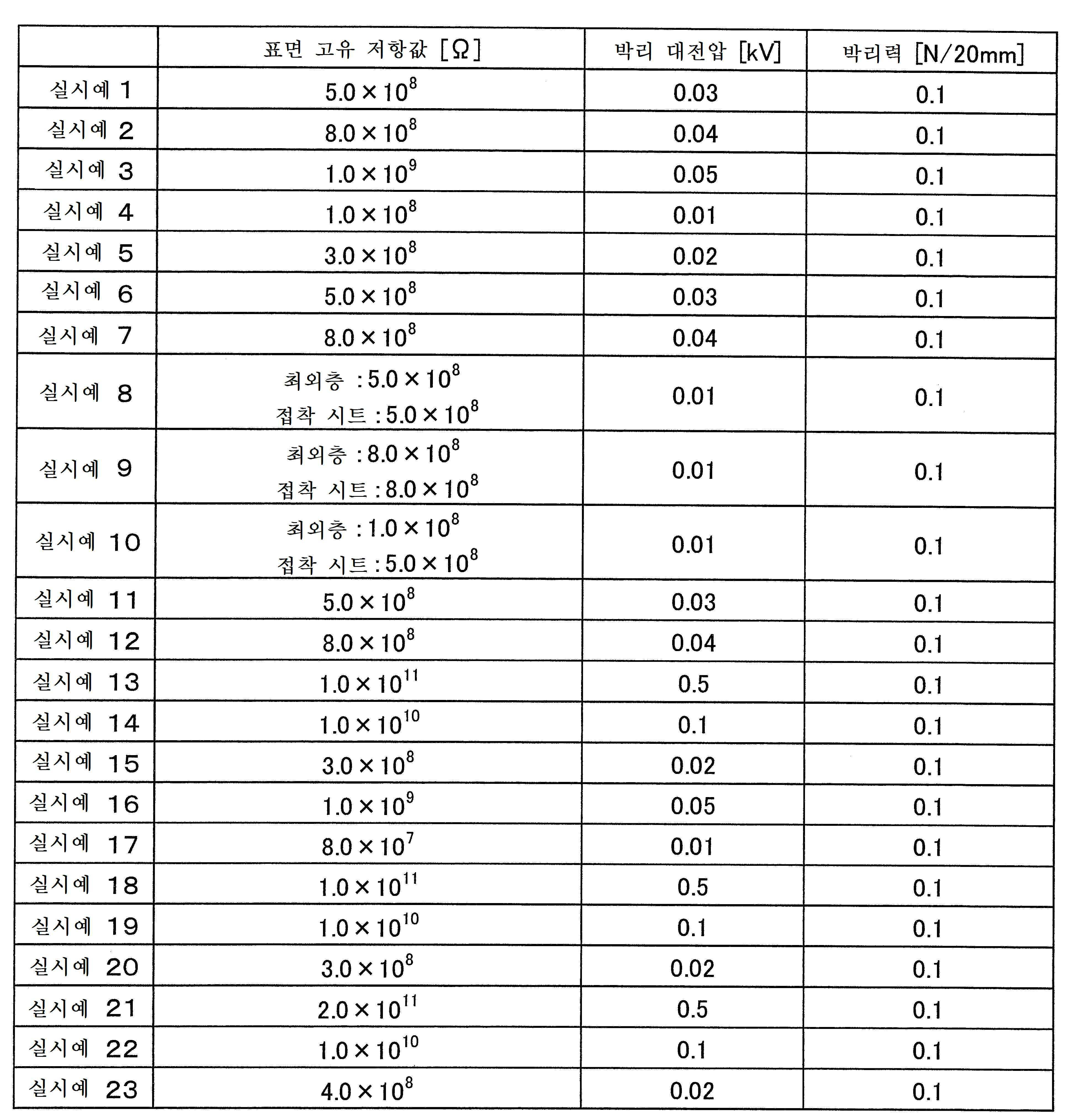
1, 10, 20: 다이싱 테이프 일체형 반도체 이면용 필름
2: 플립 칩형 반도체 이면용 필름(반도체 이면용 필름)
3: 다이싱 테이프
31: 기재
32: 점착제층
33: 반도체 웨이퍼의 점착 부분에 대응하는 부분
35, 36: 대전 방지제층
4: 반도체 웨이퍼
5: 반도체 칩
51: 반도체 칩(5)의 회로면측에 형성되어 있는 범프
6: 피착체
61: 피착체(6)의 접속 패드에 피착된 접합용 도전재
100: 아크릴판 샘플
102: 샘플 고정대1, 10 and 20: Dicing tape integrated semiconductor backing film
2: Flip-chip type semiconductor backing film (semiconductor backing film)
3: Dicing tape
31: substrate
32: pressure-sensitive adhesive layer
33: a portion corresponding to the adhesive portion of the semiconductor wafer
35, 36: Antistatic agent layer
4: Semiconductor wafer
5: Semiconductor chip
51: bumps formed on the circuit surface side of the
6: adherend
61: a conductive material for bonding bonded to the connection pad of the adherend (6)
100: acrylic plate sample
102: Sample Stands
Claims (9)
박리 속도 10m/분, 박리 각도 150°에서의 박리 시험에 있어서의, 상기 점착제층과 상기 접착 시트의 박리력이 0.02 내지 0.5N/20㎜이며,
상기 박리 시험에 의한 조건에 따라 상기 점착제층과 상기 접착 시트를 박리하였을 때의 박리 대전압의 절댓값이 0.5㎸ 이하인 것을 특징으로 하는 다이싱 테이프 일체형 접착 시트.A dicing tape-integrated adhesive sheet having a dicing tape having a pressure-sensitive adhesive layer laminated on a substrate and an adhesive sheet formed on the pressure-sensitive adhesive layer,
The peel strength of the pressure-sensitive adhesive layer and the adhesive sheet in the peeling test at a peeling speed of 10 m / min and a peeling angle of 150 is 0.02 to 0.5 N /
Wherein the peeling electrification voltage at the time of peeling the adhesive layer and the adhesive sheet according to the conditions of the peeling test is 0.5 kV or less.
상기 다이싱 테이프 일체형 접착 시트에 있어서의 접착 시트 위에 반도체 웨이퍼를 점착하는 공정과,
상기 반도체 웨이퍼를 다이싱하여 반도체 소자를 형성하는 공정과,
상기 반도체 소자를 상기 접착 시트와 함께, 다이싱 테이프의 점착제층으로부터 픽업하는 공정을 구비하는 것을 특징으로 하는 반도체 장치의 제조 방법.A method of manufacturing a semiconductor device using the dicing tape-integrated adhesive sheet according to any one of claims 1 to 7,
A step of adhering a semiconductor wafer onto the adhesive sheet in the dicing tape-integrated adhesive sheet,
A step of dicing the semiconductor wafer to form a semiconductor element,
And a step of picking up the semiconductor element from the pressure-sensitive adhesive layer of the dicing tape together with the adhesive sheet.
Applications Claiming Priority (20)
| Application Number | Priority Date | Filing Date | Title |
|---|---|---|---|
| JPJP-P-2012-269596 | 2012-12-10 | ||
| JP2012269585 | 2012-12-10 | ||
| JP2012269591 | 2012-12-10 | ||
| JPJP-P-2012-269592 | 2012-12-10 | ||
| JP2012269596 | 2012-12-10 | ||
| JP2012269586 | 2012-12-10 | ||
| JPJP-P-2012-269585 | 2012-12-10 | ||
| JP2012269592 | 2012-12-10 | ||
| JPJP-P-2012-269591 | 2012-12-10 | ||
| JPJP-P-2012-269586 | 2012-12-10 | ||
| JP2013088568A JP2014135469A (en) | 2012-12-10 | 2013-04-19 | Adhesive sheet, dicing tape integrated adhesive sheet, method for manufacturing semiconductor device, and semiconductor device |
| JPJP-P-2013-088565 | 2013-04-19 | ||
| JPJP-P-2013-088566 | 2013-04-19 | ||
| JPJP-P-2013-088567 | 2013-04-19 | ||
| JP2013088567A JP6297786B2 (en) | 2012-12-10 | 2013-04-19 | Adhesive sheet, dicing tape integrated adhesive sheet, semiconductor device manufacturing method, and semiconductor device |
| JPJP-P-2013-088568 | 2013-04-19 | ||
| JP2013088566A JP6129629B2 (en) | 2012-12-10 | 2013-04-19 | Dicing tape integrated adhesive sheet and manufacturing method of semiconductor device using dicing tape integrated adhesive sheet |
| JP2013088565A JP2014135468A (en) | 2012-12-10 | 2013-04-19 | Dicing tape integrated adhesive sheet and method for manufacturing semiconductor device using dicing tape integrated adhesive sheet |
| JPJP-P-2013-088564 | 2013-04-19 | ||
| JP2013088564A JP6077922B2 (en) | 2012-12-10 | 2013-04-19 | Dicing tape integrated adhesive sheet, semiconductor device manufacturing method using dicing tape integrated adhesive sheet, and semiconductor device |
Publications (2)
| Publication Number | Publication Date |
|---|---|
| KR20140074816A true KR20140074816A (en) | 2014-06-18 |
| KR102108102B1 KR102108102B1 (en) | 2020-05-11 |
Family
ID=50881367
Family Applications (1)
| Application Number | Title | Priority Date | Filing Date |
|---|---|---|---|
| KR1020130121712A Active KR102108102B1 (en) | 2012-12-10 | 2013-10-14 | Dicing tape integrated adhesive sheet, manufacturing method of semiconductor device using dicing tape integrated adhesive sheet, and semiconductor device |
Country Status (3)
| Country | Link |
|---|---|
| US (1) | US20140162434A1 (en) |
| KR (1) | KR102108102B1 (en) |
| CN (1) | CN103865416A (en) |
Cited By (4)
| Publication number | Priority date | Publication date | Assignee | Title |
|---|---|---|---|---|
| KR20190021410A (en) * | 2016-07-26 | 2019-03-05 | 미쓰이 가가쿠 토세로 가부시키가이샤 | Method for manufacturing semiconductor device |
| WO2019117428A1 (en) * | 2017-12-14 | 2019-06-20 | 주식회사 엘지화학 | Dicing die bonding film |
| KR20190071567A (en) * | 2017-12-14 | 2019-06-24 | 주식회사 엘지화학 | Dicing die-bonding film |
| KR20200140383A (en) * | 2018-05-17 | 2020-12-15 | 쇼와덴코머티리얼즈가부시끼가이샤 | Dicing-die-bonding integrated film, manufacturing method thereof, and manufacturing method of semiconductor device |
Families Citing this family (15)
| Publication number | Priority date | Publication date | Assignee | Title |
|---|---|---|---|---|
| EP3040389B1 (en) * | 2013-08-30 | 2021-04-21 | LINTEC Corporation | Sheet for processing semiconductor |
| KR101602782B1 (en) * | 2014-07-03 | 2016-03-11 | 주식회사 이오테크닉스 | Method for marking wafer |
| JP6549902B2 (en) * | 2015-05-27 | 2019-07-24 | 日東電工株式会社 | Dicing die bond film, method of manufacturing semiconductor device and semiconductor device |
| JP6530242B2 (en) * | 2015-06-01 | 2019-06-12 | 日東電工株式会社 | Semiconductor back surface film and its application |
| JP6589766B2 (en) * | 2015-08-18 | 2019-10-16 | 信越化学工業株式会社 | Wafer processing adhesive, wafer laminate, and thin wafer manufacturing method |
| EP3442013B1 (en) * | 2016-03-30 | 2021-01-06 | Mitsui Chemicals Tohcello, Inc. | Semiconductor device manufacturing method |
| JP7219006B2 (en) * | 2018-02-27 | 2023-02-07 | 日東電工株式会社 | Transparent conductive film laminate and method for producing transparent conductive film |
| JP7042667B2 (en) * | 2018-03-28 | 2022-03-28 | 古河電気工業株式会社 | Manufacturing method of semiconductor chip |
| KR102563869B1 (en) * | 2018-06-05 | 2023-08-04 | (주)이녹스첨단소재 | Anti- electrostatic discharge die attach film, Manufacturing method thereof and Process of dicing wafer |
| JP7159633B2 (en) * | 2018-06-15 | 2022-10-25 | 昭和電工マテリアルズ株式会社 | Dicing/die bonding integrated film and adhesive film used therefor |
| US11483937B2 (en) * | 2018-12-28 | 2022-10-25 | X Display Company Technology Limited | Methods of making printed structures |
| KR102388878B1 (en) * | 2019-10-01 | 2022-04-21 | 주식회사 엘지화학 | Surface protective film, method for producing surface protective film and method for manufacturing organic light emitting electronic device |
| CN114600225A (en) * | 2019-10-28 | 2022-06-07 | 昭和电工材料株式会社 | Film-like adhesive and method for evaluating its breakability, dicing die-bonding integrated film, method for producing the same, and semiconductor device |
| JP7609641B2 (en) * | 2021-01-15 | 2025-01-07 | 日東電工株式会社 | Adhesive sheet for protecting semiconductor elements |
| TWI832291B (en) * | 2022-06-15 | 2024-02-11 | 南亞塑膠工業股份有限公司 | Protection tape and method of processing wafer |
Citations (4)
| Publication number | Priority date | Publication date | Assignee | Title |
|---|---|---|---|---|
| JP3499957B2 (en) * | 1995-03-10 | 2004-02-23 | リンテック株式会社 | Antistatic adhesive sheet |
| US20050139973A1 (en) * | 2003-12-26 | 2005-06-30 | Takeshi Matsumura | Dicing die-bonding film |
| US20070281152A1 (en) * | 2006-06-02 | 2007-12-06 | Nitto Denko Corporation | Pressure-sensitive adhesive sheet for dicing and method for processing processed material using the same |
| JP2011228496A (en) | 2010-04-20 | 2011-11-10 | Nitto Denko Corp | Rear-surface film for flip-chip semiconductor, dicing tape integrated rear-surface film for flip-chip semiconductor, manufacturing method of semiconductor device, and flip-chip semiconductor device |
Family Cites Families (2)
| Publication number | Priority date | Publication date | Assignee | Title |
|---|---|---|---|---|
| JP4247956B2 (en) * | 2001-07-04 | 2009-04-02 | 古河電気工業株式会社 | Antistatic dicing tape |
| JP2003306654A (en) * | 2002-04-16 | 2003-10-31 | Furukawa Electric Co Ltd:The | Radiation-curable adhesive tape |
-
2013
- 2013-10-14 KR KR1020130121712A patent/KR102108102B1/en active Active
- 2013-10-17 US US14/056,596 patent/US20140162434A1/en not_active Abandoned
- 2013-12-10 CN CN201310670648.5A patent/CN103865416A/en active Pending
Patent Citations (4)
| Publication number | Priority date | Publication date | Assignee | Title |
|---|---|---|---|---|
| JP3499957B2 (en) * | 1995-03-10 | 2004-02-23 | リンテック株式会社 | Antistatic adhesive sheet |
| US20050139973A1 (en) * | 2003-12-26 | 2005-06-30 | Takeshi Matsumura | Dicing die-bonding film |
| US20070281152A1 (en) * | 2006-06-02 | 2007-12-06 | Nitto Denko Corporation | Pressure-sensitive adhesive sheet for dicing and method for processing processed material using the same |
| JP2011228496A (en) | 2010-04-20 | 2011-11-10 | Nitto Denko Corp | Rear-surface film for flip-chip semiconductor, dicing tape integrated rear-surface film for flip-chip semiconductor, manufacturing method of semiconductor device, and flip-chip semiconductor device |
Cited By (5)
| Publication number | Priority date | Publication date | Assignee | Title |
|---|---|---|---|---|
| KR20190021410A (en) * | 2016-07-26 | 2019-03-05 | 미쓰이 가가쿠 토세로 가부시키가이샤 | Method for manufacturing semiconductor device |
| WO2019117428A1 (en) * | 2017-12-14 | 2019-06-20 | 주식회사 엘지화학 | Dicing die bonding film |
| KR20190071567A (en) * | 2017-12-14 | 2019-06-24 | 주식회사 엘지화학 | Dicing die-bonding film |
| US11404301B2 (en) | 2017-12-14 | 2022-08-02 | Lg Chem, Ltd. | Dicing die-bonding film |
| KR20200140383A (en) * | 2018-05-17 | 2020-12-15 | 쇼와덴코머티리얼즈가부시끼가이샤 | Dicing-die-bonding integrated film, manufacturing method thereof, and manufacturing method of semiconductor device |
Also Published As
| Publication number | Publication date |
|---|---|
| CN103865416A (en) | 2014-06-18 |
| KR102108102B1 (en) | 2020-05-11 |
| US20140162434A1 (en) | 2014-06-12 |
Similar Documents
| Publication | Publication Date | Title |
|---|---|---|
| KR101920083B1 (en) | Adhesive film for semiconductor device, film for back surface of flip-chip semiconductor and dicing-tape-integrated film for back surface of flip-chip semiconductor | |
| KR101581643B1 (en) | Film for flip chip type semiconductor back surface and its use | |
| KR102108102B1 (en) | Dicing tape integrated adhesive sheet, manufacturing method of semiconductor device using dicing tape integrated adhesive sheet, and semiconductor device | |
| TWI446431B (en) | Film for flip chip type semiconductor back surface and dicing tape integrated film for semiconductor back surface | |
| JP6322317B2 (en) | Dicing tape integrated adhesive sheet, semiconductor device manufacturing method, and semiconductor device | |
| US9324616B2 (en) | Method of manufacturing flip-chip type semiconductor device | |
| KR101484810B1 (en) | Film for flip chip type semiconductor back surface | |
| KR20150130245A (en) | Dicing tape-integrated film for semiconductor back surface, and process for producing semiconductor device | |
| KR20150132004A (en) | Dicing tape-integrated film for semiconductor back surface, and process for producing semiconductor device | |
| US9620403B2 (en) | Adhesive sheet used in manufacture of semiconductor device, adhesive sheet integrated with dicing tape, semiconductor device, and method of manufacturing semiconductor device | |
| KR101555741B1 (en) | Film for back surface of flip-chip semiconductor | |
| JP5465284B2 (en) | Flip chip type semiconductor back film and dicing tape integrated semiconductor back film | |
| KR20130056863A (en) | Film for back surface of flip-chip semiconductor, dicing-tape-integrated film for back surface of semiconductor, process for producing semiconductor device, and flip-chip semiconductor device | |
| KR20160141664A (en) | Film for semiconductor back surface and use thereof | |
| JP6129629B2 (en) | Dicing tape integrated adhesive sheet and manufacturing method of semiconductor device using dicing tape integrated adhesive sheet | |
| JP6077922B2 (en) | Dicing tape integrated adhesive sheet, semiconductor device manufacturing method using dicing tape integrated adhesive sheet, and semiconductor device | |
| TWI615453B (en) | Cutting strip integrated type bonding sheet, manufacturing method of semiconductor device using dicing tape integrated type bonding sheet, and semiconductor device | |
| JP2014135469A (en) | Adhesive sheet, dicing tape integrated adhesive sheet, method for manufacturing semiconductor device, and semiconductor device | |
| KR20150097446A (en) | Film for flip chip type semiconductor back surface, dicing tape-integrated film for semiconductor back surface, process for producing semiconductor device, and flip chip type semiconductor device | |
| JP2014135468A (en) | Dicing tape integrated adhesive sheet and method for manufacturing semiconductor device using dicing tape integrated adhesive sheet | |
| KR101518095B1 (en) | Film for flip chip type semiconductor back surface, dicing tape-integrated film for semiconductor back surface, process for producing semiconductor device, and flip chip type semiconductor device |
Legal Events
| Date | Code | Title | Description |
|---|---|---|---|
| PA0109 | Patent application |
St.27 status event code: A-0-1-A10-A12-nap-PA0109 |
|
| PG1501 | Laying open of application |
St.27 status event code: A-1-1-Q10-Q12-nap-PG1501 |
|
| P22-X000 | Classification modified |
St.27 status event code: A-2-2-P10-P22-nap-X000 |
|
| P22-X000 | Classification modified |
St.27 status event code: A-2-2-P10-P22-nap-X000 |
|
| A201 | Request for examination | ||
| PA0201 | Request for examination |
St.27 status event code: A-1-2-D10-D11-exm-PA0201 |
|
| E902 | Notification of reason for refusal | ||
| PE0902 | Notice of grounds for rejection |
St.27 status event code: A-1-2-D10-D21-exm-PE0902 |
|
| E13-X000 | Pre-grant limitation requested |
St.27 status event code: A-2-3-E10-E13-lim-X000 |
|
| P11-X000 | Amendment of application requested |
St.27 status event code: A-2-2-P10-P11-nap-X000 |
|
| P13-X000 | Application amended |
St.27 status event code: A-2-2-P10-P13-nap-X000 |
|
| E701 | Decision to grant or registration of patent right | ||
| PE0701 | Decision of registration |
St.27 status event code: A-1-2-D10-D22-exm-PE0701 |
|
| GRNT | Written decision to grant | ||
| PR0701 | Registration of establishment |
St.27 status event code: A-2-4-F10-F11-exm-PR0701 |
|
| PR1002 | Payment of registration fee |
St.27 status event code: A-2-2-U10-U11-oth-PR1002 Fee payment year number: 1 |
|
| PG1601 | Publication of registration |
St.27 status event code: A-4-4-Q10-Q13-nap-PG1601 |
|
| P22-X000 | Classification modified |
St.27 status event code: A-4-4-P10-P22-nap-X000 |
|
| PR1001 | Payment of annual fee |
St.27 status event code: A-4-4-U10-U11-oth-PR1001 Fee payment year number: 4 |
|
| R18-X000 | Changes to party contact information recorded |
St.27 status event code: A-5-5-R10-R18-oth-X000 |
|
| PR1001 | Payment of annual fee |
St.27 status event code: A-4-4-U10-U11-oth-PR1001 Fee payment year number: 5 |
|
| R18-X000 | Changes to party contact information recorded |
St.27 status event code: A-5-5-R10-R18-oth-X000 |
|
| P22-X000 | Classification modified |
St.27 status event code: A-4-4-P10-P22-nap-X000 |
|
| P22-X000 | Classification modified |
St.27 status event code: A-4-4-P10-P22-nap-X000 |
|
| PR1001 | Payment of annual fee |
St.27 status event code: A-4-4-U10-U11-oth-PR1001 Fee payment year number: 6 |
|
| U11 | Full renewal or maintenance fee paid |
Free format text: ST27 STATUS EVENT CODE: A-4-4-U10-U11-OTH-PR1001 (AS PROVIDED BY THE NATIONAL OFFICE) Year of fee payment: 6 |