KR20140057901A - Semiconductor memory device and operating method thereof - Google Patents
Semiconductor memory device and operating method thereof Download PDFInfo
- Publication number
- KR20140057901A KR20140057901A KR1020120124235A KR20120124235A KR20140057901A KR 20140057901 A KR20140057901 A KR 20140057901A KR 1020120124235 A KR1020120124235 A KR 1020120124235A KR 20120124235 A KR20120124235 A KR 20120124235A KR 20140057901 A KR20140057901 A KR 20140057901A
- Authority
- KR
- South Korea
- Prior art keywords
- threshold voltage
- memory
- level
- memory cells
- cell
- Prior art date
- Legal status (The legal status is an assumption and is not a legal conclusion. Google has not performed a legal analysis and makes no representation as to the accuracy of the status listed.)
- Granted
Links
Images


Classifications
-
- G—PHYSICS
- G11—INFORMATION STORAGE
- G11C—STATIC STORES
- G11C16/00—Erasable programmable read-only memories
- G11C16/02—Erasable programmable read-only memories electrically programmable
- G11C16/06—Auxiliary circuits, e.g. for writing into memory
- G11C16/10—Programming or data input circuits
-
- G—PHYSICS
- G11—INFORMATION STORAGE
- G11C—STATIC STORES
- G11C11/00—Digital stores characterised by the use of particular electric or magnetic storage elements; Storage elements therefor
- G11C11/56—Digital stores characterised by the use of particular electric or magnetic storage elements; Storage elements therefor using storage elements with more than two stable states represented by steps, e.g. of voltage, current, phase, frequency
- G11C11/5621—Digital stores characterised by the use of particular electric or magnetic storage elements; Storage elements therefor using storage elements with more than two stable states represented by steps, e.g. of voltage, current, phase, frequency using charge storage in a floating gate
- G11C11/5642—Sensing or reading circuits; Data output circuits
-
- G—PHYSICS
- G11—INFORMATION STORAGE
- G11C—STATIC STORES
- G11C11/00—Digital stores characterised by the use of particular electric or magnetic storage elements; Storage elements therefor
- G11C11/56—Digital stores characterised by the use of particular electric or magnetic storage elements; Storage elements therefor using storage elements with more than two stable states represented by steps, e.g. of voltage, current, phase, frequency
- G11C11/5621—Digital stores characterised by the use of particular electric or magnetic storage elements; Storage elements therefor using storage elements with more than two stable states represented by steps, e.g. of voltage, current, phase, frequency using charge storage in a floating gate
- G11C11/5628—Programming or writing circuits; Data input circuits
- G11C11/5635—Erasing circuits
-
- G—PHYSICS
- G11—INFORMATION STORAGE
- G11C—STATIC STORES
- G11C16/00—Erasable programmable read-only memories
- G11C16/02—Erasable programmable read-only memories electrically programmable
- G11C16/06—Auxiliary circuits, e.g. for writing into memory
- G11C16/34—Determination of programming status, e.g. threshold voltage, overprogramming or underprogramming, retention
-
- G—PHYSICS
- G11—INFORMATION STORAGE
- G11C—STATIC STORES
- G11C16/00—Erasable programmable read-only memories
- G11C16/02—Erasable programmable read-only memories electrically programmable
- G11C16/04—Erasable programmable read-only memories electrically programmable using variable threshold transistors, e.g. FAMOS
- G11C16/0483—Erasable programmable read-only memories electrically programmable using variable threshold transistors, e.g. FAMOS comprising cells having several storage transistors connected in series
-
- G—PHYSICS
- G11—INFORMATION STORAGE
- G11C—STATIC STORES
- G11C2216/00—Indexing scheme relating to G11C16/00 and subgroups, for features not directly covered by these groups
- G11C2216/12—Reading and writing aspects of erasable programmable read-only memories
- G11C2216/14—Circuits or methods to write a page or sector of information simultaneously into a nonvolatile memory, typically a complete row or word line in flash memory
Landscapes
- Engineering & Computer Science (AREA)
- Computer Hardware Design (AREA)
- Read Only Memory (AREA)
Abstract
반도체 메모리 장치 및 이의 동작 방법은 프로그램 동작 시 메모리 셀의 상태에 따라 셀 단위 소거 동작을 실시함으로써 메모리 셀들의 문턱전압이 양의 방향과 음의 방향으로 변경된다. 따라서 전체적인 메모리 셀의 문턱전압 변화량이 감소하고 간섭 현상으로 인한 메모리 셀들의 문턱전압 분포의 변동도 감소한다. A semiconductor memory device and an operation method thereof perform a cell-by-cell erase operation according to the state of a memory cell during a program operation so that the threshold voltages of the memory cells are changed in positive and negative directions. Therefore, the threshold voltage variation of the entire memory cell decreases and the variation of the threshold voltage distribution of the memory cells due to the interference phenomenon also decreases.
Description
본 발명은 반도체 메모리 장치 및 반도체 메모리 장치의 동작 방법에 관한 것이다.The present invention relates to a semiconductor memory device and a method of operating the semiconductor memory device.
반도체 메모리 장치는 크게 휘발성 메모리 장치(Volatile memory device)와 불휘발성 메모리 장치(Non-volatile memory device)로 구분된다. Semiconductor memory devices are classified into a volatile memory device and a non-volatile memory device.
휘발성 메모리 장치는 쓰기 및 읽기 속도가 빠르지만 전원 공급이 차단되면 저장된 데이터가 소멸된다. 불휘발성 메모리 장치는 쓰기 및 읽기 속도가 상대적으로 느리지만 전원 공급이 차단되더라도 저장된 데이터를 유지한다. 따라서 전원 공급 여부와 관계없이 유지되어야 할 데이터를 저장하기 위해 불휘발성 메모리 장치가 사용된다. 불휘발성 메모리 장치에는 ROM(Read-Only Memory), MROM(Mask ROM), PROM(Programmable ROM), EPROM(Erasable Programmable ROM), EEPROM(Electrically Erasable Programmable ROM), 플래시 메모리(Flash memory), PRAM(Phase-change Random Access Memory), MRAM(Magnetic RAM), RRAM(Resistive RAM), FRAM(Ferroelectric RAM) 등이 있다. 플래시 메모리는 노어 타입과 낸드 타입으로 구분된다.The volatile memory device has a fast write and read speed, but the stored data is lost when the power supply is interrupted. A non-volatile memory device maintains stored data even if the write and read rates are relatively slow, but the power supply is interrupted. Therefore, a nonvolatile memory device is used to store data to be maintained regardless of power supply. A nonvolatile memory device includes a ROM (Read Only Memory), a MROM (Mask ROM), a PROM (Programmable ROM), an EPROM (Erasable Programmable ROM), an EEPROM (Electrically Erasable Programmable ROM) (Random Access Memory), MRAM (Magnetic RAM), RRAM (Resistive RAM) and FRAM (Ferroelectric RAM). Flash memory is divided into NOR type and NOR type.
플래시 메모리는 데이터의 프로그램과 소거가 자유로운 RAM의 장점과 전원 공급이 차단되어도 저장된 데이터를 보존할 수 있는 ROM의 장점을 가진다. 플래시 메모리는 디지털 카메라, PDA(Personal Digital Assistant) 및 MP3 플레이어와 같은 휴대용 전자기기의 저장 매체로 널리 사용되고 있다.Flash memory has the advantages of RAM, which is free to program and erase data, and ROM, which can save stored data even when power supply is cut off. Flash memories are widely used as storage media for portable electronic devices such as digital cameras, PDAs (Personal Digital Assistants) and MP3 players.
최근에, 집적도를 높이기 위해 메모리 셀들의 크기가 작아지고 메모리 셀들 간의 간격이 좁아지면서 간섭 현상(interference) 등으로 인해 메모리 셀들의 문턱전압분포가 나빠지는 문제점이 있다. In recent years, there has been a problem that the threshold voltage distribution of memory cells is deteriorated due to interference due to a decrease in the size of the memory cells and an interval between the memory cells in order to increase the degree of integration.
본 발명의 실시예는 메모리 셀들의 문턱전압 분포를 개선할 수 있는 반도체메모리 장치 및 반도체 메모리 장치의 동작 방법을 제공한다.An embodiment of the present invention provides a semiconductor memory device capable of improving the threshold voltage distribution of memory cells and a method of operating the semiconductor memory device.
반도체 메모리 장치의 동작 방법은 제1 상태의 메모리 셀들에 LSB 프로그램 동작을 실시하여 문턱전압을 상승시키는 단계, MSB 프로그램 동작 시 상기 메모리 셀들 중 제2 상태로 프로그램할 메모리 셀의 문턱전압을 제1 레벨 이하로 하강시키는 단계, 및 상기 메모리 셀들 중 제3 상태로 프로그램할 메모리 셀의 문턱전압을 상기 제1 레벨 보다 높은 제2 레벨 이상으로 상승시키고 상기 메모리 셀들 중 제4 상태로 프로그램할 메모리 셀의 문턱전압을 상기 제2 레벨 보다 높은 제3 레벨 이상으로 상승시키는 단계를 포함한다.A method of operating a semiconductor memory device includes: increasing a threshold voltage by performing an LSB programming operation on memory cells in a first state; increasing a threshold voltage of a memory cell to be programmed to a second state of the memory cells, And raising a threshold voltage of a memory cell to be programmed to a third one of the memory cells above a second level higher than the first level and resetting a threshold of a memory cell to be programmed to a fourth of the memory cells And raising the voltage to a third level or higher, which is higher than the second level.
반도체 메모리 장치의 동작 방법은 멀티 비트 데이터를 프로그램하기 위한 제1 페이지의 메모리 셀들 중 제1 데이터를 저장할 메모리 셀의 문턱전압을 제1 레벨 이하로 하강시키는 단계, 및 상기 메모리 셀들 중 제2 데이터를 저장할 메모리 셀의 문턱전압을 상기 제1 레벨 보다 높은 제2 레벨 이상으로 상승시키는 단계를 포함한다.A method of operating a semiconductor memory device includes: dropping a threshold voltage of a memory cell for storing first data of memory cells of a first page for programming multi-bit data below a first level; And raising a threshold voltage of a memory cell to be stored to a second level or higher than the first level.
반도체 메모리 장치는 메모리 셀들을 포함하는 메모리 어레이, 제1 상태의 메모리 셀들에 LSB 프로그램 동작 및 MSB 프로그램 동작을 실시하도록 구성된 동작회로, 및 상기 MSB 프로그램 동작 시 제2 상태로 프로그램할 메모리 셀의 문턱전압을 제1 레벨 이하로 하강시키고 상기 메모리 셀들 중 제3 상태로 프로그램할 메모리 셀의 문턱전압을 상기 제1 레벨 보다 높은 제2 레벨 이상으로 상승시키고 상기 메모리 셀들 중 제4 상태로 프로그램할 메모리 셀의 문턱전압을 상기 제2 레벨 보다 높은 제3 레벨 이상으로 상승시키도록 상기 동작회로를 제어하는 제어회로를 포함한다.The semiconductor memory device includes a memory array including memory cells, an operation circuit configured to perform LSB program operation and MSB program operation on the memory cells in the first state, and a memory circuit including a threshold voltage Of a memory cell to be programmed to a third one of the memory cells and to raise a threshold voltage of a memory cell to be programmed to a third of the memory cells to a second level higher than the first level, And a control circuit for controlling the operation circuit to raise the threshold voltage to a third level or higher, which is higher than the second level.
반도체 메모리 장치는 메모리 셀들을 포함하는 메모리 어레이, 상기 메모리 셀들의 문턱전압을 상승 또는 하강시키도록 구성된 동작회로, 및 멀티 비트 데이터를 프로그램하기 위한 제1 페이지의 메모리 셀들 중 제1 데이터를 저장할 메모리 셀의 문턱전압을 제1 레벨 이상으로 상승시키고, 상기 메모리 셀들 중 제2 데이터를 저장할 메모리 셀의 문턱전압을 상기 제1 레벨 보다 낮은 제2 레벨 이하로 하강시키도록 상기 동작 회로를 제어하는 제어회로를 포함한다.A semiconductor memory device includes a memory array including memory cells, an operating circuit configured to raise or lower a threshold voltage of the memory cells, and a memory cell for storing first data of memory cells of a first page for programming multi- And a control circuit for controlling the operation circuit to lower the threshold voltage of the memory cell storing the second data among the memory cells to a second level lower than the first level .
본 발명의 실시예에 따른 반도체메모리 장치 및 반도체 메모리 장치의 동작 방법에 의하면 간섭 현상으로 인해 메모리 셀의 문턱전압이 변경되는 것을 감소시켜 메모리 셀들의 문턱전압분포를 개선할 수 있다.According to the semiconductor memory device and the operation method of the semiconductor memory device according to the embodiment of the present invention, the threshold voltage distribution of the memory cell can be improved by the interference phenomenon, thereby improving the threshold voltage distribution of the memory cells.
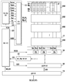
도 1은 본 발명의 실시예에 따른 반도체 메모리 장치를 설명하기 위한 블록도이다.
도 2는 도 1에 도시된 메모리 블록을 설명하기 위한 회로도이다.
도 3은 도 1에 도시된 페이지 버퍼를 설명하기 위한 회로도이다.
도 4는 본 발명의 일 실시예에 따른 반도체 메모리 장치의 동작 방법을 설명하기 위한 도식도이다.
도 5는 본 발명의 다른 실시예에 따른 반도체 메모리 장치의 동작 방법을 설명하기 위한 도식도이다.
도 6은 본 발명의 또 다른 실시예에 따른 반도체 메모리 장치의 동작 방법을 설명하기 위한 도식도이다.
도 7은 도 6의 반도체 메모리 장치의 동작 방법을 설명하기 위한 흐름도이다.
도 8은 도 7의 반도체 메모리 장치의 동작 방법에서 프로그램 순서를 설명하기 위한 도면이다.
도 9는 도 7의 반도체 메모리 장치의 동작 방법에서 셀 단위 소거 동작을 설명하기 위한 도면이다.
도 10은 도 7의 반도체 메모리 장치의 동작 방법 중 일반 프로그램 동작과 셀 단위 소거 동작 시의 전압 인가 조건을 설명하기 위한 도면이다.
도 11은 본 발명의 실시예에 따른 메모리 시스템을 간략히 보여주는 블록도이다.
도 12는 앞서 설명된 다양한 실시예들에 따라 프로그램 동작을 수행하는 퓨전 메모리 장치 또는 퓨전 메모리 시스템을 간략히 보여주는 블록도이다.
도 13은 본 발명의 실시예에 따른 플래시 메모리 장치를 포함한 컴퓨팅 시스템을 간략히 보여주는 블록도이다.1 is a block diagram illustrating a semiconductor memory device according to an embodiment of the present invention.
Fig. 2 is a circuit diagram for explaining the memory block shown in Fig. 1. Fig.
3 is a circuit diagram for explaining the page buffer shown in FIG.
4 is a schematic diagram illustrating a method of operating a semiconductor memory device according to an embodiment of the present invention.
5 is a schematic diagram illustrating a method of operating a semiconductor memory device according to another embodiment of the present invention.
6 is a schematic diagram illustrating a method of operating a semiconductor memory device according to another embodiment of the present invention.
7 is a flowchart for explaining an operation method of the semiconductor memory device of FIG.
8 is a diagram for explaining a program procedure in the operation method of the semiconductor memory device of FIG.
9 is a diagram for explaining a cell-by-cell erase operation in the operation method of the semiconductor memory device of FIG.
FIG. 10 is a view for explaining general program operation and voltage application conditions in a cell-by-cell erase operation in the method of operation of the semiconductor memory device of FIG.
11 is a block diagram briefly showing a memory system according to an embodiment of the present invention.
12 is a simplified block diagram illustrating a fusion memory device or a fusion memory system that performs program operation in accordance with various embodiments described above.
13 is a block diagram briefly showing a computing system including a flash memory device according to an embodiment of the present invention.
이하, 첨부된 도면을 참조하여 본 발명의 바람직한 실시예를 설명하기로 한다. 그러나, 본 발명은 이하에서 개시되는 실시예에 한정되는 것이 아니라 서로 다른 다양한 형태로 구현될 수 있으며, 본 발명의 범위가 다음에 상술하는 실시예에 한정되는 것은 아니다. 단지 본 실시예는 본 발명의 개시가 완전하도록 하며 통상의 지식을 가진 자에게 발명의 범주를 완전하게 알려주기 위해 제공되는 것이며, 본 발명의 범위는 본원의 특허 청구 범위에 의해서 이해되어야 한다. Hereinafter, preferred embodiments of the present invention will be described with reference to the accompanying drawings. However, the present invention is not limited to the embodiments described below, but may be implemented in various forms, and the scope of the present invention is not limited to the embodiments described below. It is to be understood that both the foregoing general description and the following detailed description are exemplary and explanatory and are intended to provide further explanation of the invention as claimed.
도 1은 본 발명의 실시예에 따른 반도체 메모리 장치를 설명하기 위한 회로도이다. 도 2는 도 1에 도시된 메모리 블록을 설명하기 위한 회로도이다. 1 is a circuit diagram for explaining a semiconductor memory device according to an embodiment of the present invention. Fig. 2 is a circuit diagram for explaining the memory block shown in Fig. 1. Fig.
본 발명의 실시예에 따른 반도체 메모리 장치는 다수의 메모리 블록들(110MB)을 포함하는 메모리 어레이(110), 메모리 블록(110MB)의 선택된 페이지에 포함된 메모리 셀들의 프로그램 동작, 리드 동작 및 소거 동작을 수행하도록 구성된 동작 회로(130, 140, 150, 160, 170, 180), 동작 회로(130, 140, 150, 160, 170, 180)를 제어하도록 구성된 제어 회로(120)를 포함한다. NAND 플래시 메모리 장치의 경우, 동작 회로는 전압 공급 회로(135), 페이지 버퍼 그룹(150), 컬럼 선택 회로(160), 입출력 회로(170) 및 패스/페일 체크 회로(180)를 포함한다.A semiconductor memory device according to an embodiment of the present invention includes a
메모리 어레이(110)는 복수의 메모리 블록들(110MB)을 포함한다. The
도 2를 참조하면, 각각의 메모리 블록은 비트라인들(BLe1~BLek, BLo1~BLok)과 공통 소스 라인(CSL) 사이에 연결된 다수의 스트링들(STe1~STek, STo1~STok)을 포함한다. 즉, 스트링들(STe1~STok)은 대응하는 비트 라인들(BLe1~BLok)과 각각 연결되고 공통 소스 라인(CSL)과 공통으로 연결된다. 각각의 스트링(STe1)은 소스가 공통 소스 라인(CSL)에 연결되는 소스 셀렉트 트랜지스터(SST), 복수의 메모리 셀들(C0e1~Cne1), 그리고 드레인이 비트라인(BLe1)에 연결되는 드레인 셀렉트 트랜지스터(DST)를 포함한다. 메모리 셀들(C0e1~Cne1)은 셀렉트 트랜지스터들(SST, DST) 사이에 직렬로 연결된다. 소스 셀렉트 트랜지스터(SST)의 게이트는 소스 셀렉트 라인(SSL)에 연결되고, 메모리 셀들(C0e1~Cne1)의 게이트들은 워드라인들(WL0~WLn)에 각각 연결되며, 드레인 셀렉트 트랜지스터(DST)의 게이트는 드레인 셀렉트 라인(DSL)에 연결된다. Referring to FIG. 2, each memory block includes a plurality of strings STe1 to STek, STo1 to SToK connected between bit lines BLe1 to BLek, BLo1 to BLok and a common source line CSL. That is, the strings STe1 to STok are connected to the corresponding bit lines BLe1 to BLok, respectively, and are connected in common to the common source line CSL. Each string STe1 includes a source select transistor SST having a source connected to the common source line CSL, a plurality of memory cells C0e1 to Cne1, and a drain select transistor (drain) connected to the bit line BLe1 DST). The memory cells C0e1 to Cne1 are connected in series between the select transistors SST and DST. The gates of the source select transistors SST are connected to the source select line SSL and the gates of the memory cells C0e1 to Cne1 are connected to the word lines WL0 to WLn respectively and the gate of the drain select transistor DST Is connected to a drain select line (DSL).
스트링들(STe1~STok)은 셀 단위의 소거 동작이 가능하도록 하기 위해 구조가 변경된다. 종래에는 스트링들(STe1~STok) 하부에 p웰 영역이 형성되어 있지만, 본 발명은 p웰 영역을 감싸는 n웰 영역이 있고, 상기 n웰 영역을 감싸는 p웰 영역이 있는 셀 구조를 갖는다. 이에 대해서는 후술하기로 한다. The strings STe1 to STok are changed in structure to enable the erase operation on a cell-by-cell basis. Conventionally, a p-well region is formed under the strings STe1 to STok. However, the present invention has an n-well region surrounding the p-well region and a p-well region surrounding the n-well region. This will be described later.
낸드 플래시 메모리 장치에서 메모리 블록에 포함된 메모리 셀들은 물리적 페이지 단위 또는 논리적 페이지 단위로 구분할 수 있다. 예를 들어, 하나의 워드라인(예, WL0)에 연결된 메모리 셀들(C0e1~C0ek, C0o1~C0ok)이 하나의 물리적 페이지(PAGE0)를 구성한다. 또한, 하나의 워드라인(예, WL0)에 연결된 짝수 번째 메모리 셀들(C0e1~C0ek)이 하나의 이븐 물리적 페이지를 구성하고, 홀수 번째 메모리 셀들(C0o1~C0ok)이 하나의 오드 물리적 페이지를 구성할 수 있다. 이러한 페이지(또는, 이븐 페이지와 오드 페이지)는 프로그램 동작 또는 리드 동작의 기본 단위가 된다. In a NAND flash memory device, memory cells included in a memory block can be divided into a physical page unit or a logical page unit. For example, memory cells (C0e1 to C0ek, C0o1 to C0ok) connected to one word line (e.g., WL0) constitute one physical page (PAGE0). Further, even-numbered memory cells C0e1 to C0ek connected to one word line (e.g., WL0) constitute one even physical page, and odd-numbered memory cells (C0o1 to C0ok) constitute one odd physical page . These pages (or even pages and odd pages) are the basic unit of program operation or read operation.
다시, 도 1 및 도 2를 참조하면, 제어 회로(120)는 외부로부터 입출력 회로(170)를 통해 입력되는 명령 신호(CMD)에 응답하여 프로그램 동작, 검증 동작, 리드 동작 또는 소거 동작을 수행하기 위해 필요한 전압을 생성하기 위한 전압 제어 신호(VCON)를 출력하고, 동작의 종류에 따라 페이지 버퍼 그룹(150)에 포함된 페이지 버퍼들(PB1~PBk)을 제어하기 위한 PB 제어 신호들(PBCON)을 출력한다. 제어 회로(120)가 페이지 버퍼 그룹(150)을 제어하는 동작은 후술하기로 한다. 또한, 제어 회로(120)는 입출력 회로(170)를 통해 외부로부터 입력되는 어드레스 신호(ADD)에 응답하여 로우 어드레스 신호(RADD)와 컬럼 어드레스 신호(CADD)를 출력한다. 1 and 2, the
전압 공급 회로(135)는 제어 회로(120)의 전압 제어 신호(VCON)에 응답하여 메모리 셀들의 프로그램 동작, 리드 동작 및 소거 동작에 필요한 동작 전압들(예, Verase, Vpgm, Vread, Vpass, Vvfy, Vdsl, Vssl, Vcsl)을 선택된 메모리 블록의 드레인 셀렉트 라인(DSL), 워드라인들(WL0~WLn) 및 소스 셀렉트 라인(SSL)를 포함하는 로컬 라인들로 공급한다. 전압 공급 회로(135)는 비트라인전압을 공급하도록 구성될 수 있다. 이러한 전압 공급 회로(135)는 전압 생성 회로(130) 및 로우 디코더(140)를 포함한다. The
전압 생성 회로(130)는 제어 회로(120)의 전압 제어 신호(VCON)에 응답하여 메모리 셀들의 프로그램 동작, 리드 동작, 또는 소거 동작에 필요한 동작 전압들(예, Verase, Vpgm, Vread, Vpass, Vvfy, Vdsl, Vssl, Vcsl)을 글로벌 라인들로 출력한다. 예를 들어, 프로그램 동작을 위해 전압 생성 회로(130)는 선택된 페이지의 메모리 셀들에 인가하기 위한 프로그램 전압(Vpgm) 및 비선택된 메모리 셀들에 인가하기 위한 패스 전압(Vpass)을 글로벌 라인들로 출력한다. 리드 동작을 위해 전압 생성 회로(130)는 선택된 페이지의 메모리 셀들에 인가하기 위한 리드 전압(Vread) 및 비선택된 메모리 셀들에 인가하기 위한 패스 전압(Vpass)을 글로벌 라인들로 출력한다. 소거 동작을 위해 전압 생성 회로(130)는 선택된 메모리 블록의 메모리 셀들에 인가하기 위한 소거 전압(Verase)을 글로벌 라인들로 출력한다. 특히, 셀 단위 소거 동작을 위해 전압 생성 회로(130)는 드레인 셀렉트 라인(DSL)에 인가하기 위한 전압(Vdsl)과 비트라인전압을 조절하여 출력한다. The
로우 디코더(140)는 제어 회로(120)의 로우 어드레스 신호들(RADD)에 응답하여, 전압 생성 회로(130)에서 글로벌 라인들로 출력된 동작 전압들이 메모리 어레이(110)에서 선택된 메모리 블록(110MB)의 로컬 라인들(DSL, WL0~WLn, SSL)로 전달될 수 있도록 글로벌 라인들과 로컬 라인들(DSL, WL0~WLn, SSL)을 연결한다. 이로써, 선택된 셀(예, C0e1)과 연결된 로컬 워드라인(예, WL0)에는 전압 생성 회로(130)로부터 글로벌 워드라인을 통해 프로그램 전압(Vpgm) 또는 리드 전압(Vread)이 인가된다. 그리고, 선택되지 않은 셀들(C1e1~Cne1)과 연결된 로컬 워드라인들(예, WL1~WLn)에는 전압 생성 회로(130)로부터 글로벌 워드라인들을 통해 패스 전압(Vpass)이 인가된다. 소거 동작에서는 블록 내의 메모리 셀들 전체에 소거 전압(Verase)이 인가될 수 있다. 이에 따라, 선택된 셀(C0e1)에 데이터가 프로그램 전압(Vpgm)에 의해 저장되거나, 선택된 셀(C0e1)에 저장된 데이터가 리드 전압(Vread)에 의해 독출된다. The
페이지 버퍼 그룹들(150)은 비트라인들(BLe1~BLek, BLo1~BLok)을 통해 메모리 어레이(110)와 연결되는 다수의 페이지 버퍼들(PB1~PBk)을 각각 포함한다. 페이지 버퍼 그룹(150)의 페이지 버퍼들(PB1~PBk)은 제어 회로(120)의 PB 제어 신호(PBCON)에 응답하여 메모리 셀들(C0e1~C0ek 또는 C0o1~C0ok)에 데이터를 저장하기 위하여 입력되는 데이터에 따라 비트라인들(BLe1~BLek 또는 BLo1~BLok)을 선택적으로 프리차지하거나, 메모리 셀들(C0e1~C0ek 또는 C0o1~C0ok)로부터 데이터를 독출하기 위하여 비트라인들(BLe1~BLek 또는 BLo1~BLok)의 전압을 센싱한다. The
예를 들어, 메모리 셀(C0e1)에 저장하기 위해 프로그램 데이터(예, '0' 데이터)가 페이지 버퍼(PB1)로 입력되면, 프로그램 동작에서 페이지 버퍼(PB1)는 프로그램 데이터가 저장되는 메모리 셀(C0e1)의 비트라인(BLe1)에 프로그램 허용 전압(예, 접지 전압)을 인가한다. 그 결과, 메모리 셀(C0e1)의 문턱전압은 프로그램 동작에서 워드라인(WL0)에 인가되는 프로그램 전압(Vpgm)과 비트라인(BLe1)에 인가되는 프로그램 허용 전압에 의해 상승한다. 그리고, 메모리 셀(C0e1)에 저장하기 위해 소거 데이터(예, '1' 데이터)가 페이지 버퍼(PB1)로 입력되면, 프로그램 동작에서 페이지 버퍼(PB1)는 소거 데이터가 저장되는 메모리 셀(C0e1)의 비트라인(BLe1)에 프로그램 금지 전압(예, 전원 전압)을 인가한다. 그 결과, 프로그램 동작에서 워드라인(WL0)에 프로그램 전압(Vpgm)이 인가되더라도 비트라인(BLe1)에 인가되는 프로그램 금지 전압에 의해 메모리 셀(C0e1)의 문턱전압은 상승하지 않는다. 이렇게 문턱전압이 서로 달라짐에 따라, 메모리 셀에는 서로 다른 데이터가 저장될 수 있다.For example, when program data (e.g., '0' data) is input to the page buffer PB1 for storage in the memory cell C0e1, in the program operation, the page buffer PB1 stores the program data (E. G., Ground voltage) to the bit line BLe1 of the memory cell array C0e1. As a result, the threshold voltage of the memory cell C0e1 rises by the program voltage Vpgm applied to the word line WL0 in the programming operation and the program allowable voltage applied to the bit line BLe1. When the erase data (e.g., '1' data) is input to the page buffer PB1 to be stored in the memory cell C0e1, in the program operation, the page buffer PB1 stores the erase data in the memory cell C0e1, (For example, power supply voltage) to the bit line BLe1 of the bit line BLe1. As a result, even if the program voltage Vpgm is applied to the word line WL0 in the program operation, the threshold voltage of the memory cell C0e1 does not rise due to the program inhibition voltage applied to the bit line BLe1. As the threshold voltages are different from each other, different data can be stored in the memory cell.
한편, 리드 동작에서, 페이지 버퍼 그룹(150)은 이븐 비트라인들(BLe1~BLek)과 오드 비트라인들(BLo1~BLok) 중 선택된 비트라인들(예, BLe1~BLek)을 모두 프리차지하고 비선택 비트라인들(예, BLo1~BLok)을 모두 디스차지한다. 그리고, 전압 공급 회로(135)로부터 선택된 워드라인(WL0)에 리드 전압(Vread)이 인가되면, 프로그램 데이터가 저장된 메모리 셀들의 비트라인들은 프리차지 상태를 유지하고, 소거 데이터가 저장된 메모리 셀들의 비트라인들은 디스차지된다. 페이지 버퍼 그룹(150)은 비트라인들(BLe1~BLek)의 전압 변화를 센싱하고, 센싱 결과에 대응하는 메모리 셀들의 데이터를 래치한다. On the other hand, in the read operation, the
페이지 버퍼의 구체적인 구성은 후술하기로 한다. The specific configuration of the page buffer will be described later.
컬럼 선택 회로(160)는 제어 회로(120)에서 출력된 컬럼 어드레스 신호(CADD)에 응답하여 페이지 버퍼 그룹(150)에 포함된 페이지 버퍼들(PB1~PBk)을 선택한다. 즉, 컬럼 선택 회로(160)는 메모리 셀들에 저장될 데이터를 컬럼 어드레스 신호(CADD)에 응답하여 순차적으로 페이지 버퍼들(PB1~PBk)로 전달한다. 또한, 리드 동작에 의해 페이지 버퍼들(PB1~PBk)에 래치된 메모리 셀들의 데이터가 외부로 출력될 수 있도록 컬럼 어드레스 신호(CADD)에 응답하여 순차적으로 페이지 버퍼들(PB1~PBk)을 선택한다. The
입출력 회로(170)는 프로그램 동작 시 메모리 셀들에 저장하기 위해 외부로부터 입력된 데이터를 페이지 버퍼 그룹(150)으로 입력하기 위하여 제어 회로(120)의 제어에 따라 데이터를 컬럼 선택 회로(160)에 전달한다. 컬럼 선택 회로(160)는 입출력 회로(170)로부터 전달된 데이터를 앞서 설명한 방식에 따라 페이지 버퍼 그룹(150)의 페이지 버퍼들(PB1~PBk)로 전달하면 페이지 버퍼들(PB1~PBk)은 입력된 데이터를 내부의 래치 회로에 저장한다. 또한, 리드 동작 시 입출력 회로(170)는 페이지 버퍼 그룹(150)의 페이지 버퍼들(PB1~PBk)로부터 컬럼 선택 회로(160)를 통해 전달된 데이터를 외부로 출력한다.The input /
패스/페일 체크 회로(180)는 프로그램 동작 후에 실시되는 프로그램 검증 동작에서 페이지 버퍼들(PB1~PBk)로부터 각각 출력되는 비교 결과 신호들에 응답하여 패스/페일 신호(PFS)를 출력한다. 구체적으로 설명하면, 프로그램 검증 동작에서 메모리 셀의 문턱전압과 목표 전압을 비교하고 그 결과값이 페이지 버퍼들(PB1~PBk)의 내부 래치 회로에 래치된다. 그리고, 래치된 비교 결과 신호들은 패스/페일 체크 회로(180)로 출력된다. 패스/페일 체크 회로(180)는 비교 결과 신호들에 응답하여 프로그램 동작의 완료 여부를 나타내는 패스/페일 신호(PFS)를 제어 회로(120)로 출력한다. 제어 회로(120)는 패스/페일 신호(PFS)에 응답하여 프로그램 데이터가 저장되는 메모리 셀들 중 문턱전압이 목표 전압보다 낮은 메모리 셀이 존재하는지를 판단하고, 그 결과에 따라 프로그램 동작의 재실시 여부를 결정한다. The pass /
특히, 제어회로(120)는 셀 단위의 소거 동작을 실시하도록 동작회로를 제어한다. 제어회로(120)는 제1 데이터를 저장하는 메모리 셀은 프로그램 동작을 실시하여 문턱전압을 제1 레벨 이상으로 상승시키고 제2 데이터를 저장하는 메모리 셀은 셀 단위 소거 동작을 실시하여 문턱전압을 제1 레벨 보다 낮은 제2 레벨 이하로 하강시키도록 동작회로를 제어한다.In particular, the
셀 단위 소거 동작은 GIDL(Gate Induced Drain Leakage) 소거를 이용하여 수행되는데, 이에 대해서는 후술하기로 한다. The cell-by-cell erase operation is performed using GIDL (Gate Induced Drain Leakage) erase, which will be described later.
도 3은 도 1에 도시된 페이지 버퍼를 설명하기 위한 회로도이다. 3 is a circuit diagram for explaining the page buffer shown in FIG.
도 3을 참조하면, 페이지 버퍼(PB1)는 제어 회로(도 1의 120)의 제어에 따라 동작하며, 이하에서 설명되는 신호들(PRECHb, TRAN, RST, SET, PBSENSE, BSELe, BSELo, DISCHe, DISCHo)은 제어 회로에서 출력될 수 있다. Referring to FIG. 3, the page buffer PB1 operates under the control of the control circuit 120 (FIG. 1), and the signals (PRECHb, TRAN, RST, SET, PBSENSE, BSELe, BSELo, DISCHe, DISCHo) can be output from the control circuit.
페이지 버퍼(PB1)는 비트라인 연결 회로(BLC), 프리차지 회로(P101) 및 다수의 래치 회로들(LC1~LC3)을 포함한다. The page buffer PB1 includes a bit line connection circuit BLC, a precharge circuit P101 and a plurality of latch circuits LC1 through LC3.
비트라인 연결 회로(BLC)의 스위칭 소자들(N105, N107)은 비트라인 선택 신호들(BSELe, BSELo)에 응답하여 이븐 비트라인(BLe1) 및 오드 비트라인(BLo1) 중 하나의 비트라인을 선택하고, 스위칭 소자들(N101, N103)은 디스차지 신호들(DISCHe, DISCHo)에 응답하여 프로그램 동작 시 비선택된 비트라인을 프리차지하거나 리드 동작 시 비선택된 비트라인을 디스차지하는 동작을 수행한다. 스위칭 소자(N109)는 스위칭 소자들(N105, N107)에 의해 선택된 비트라인과 래치 회로들(LC1~LC3) 중 하나의 래치 회로를 연결 신호(PBSENSE)에 응답하여 연결하는 동작을 수행한다. 래치 회로들(LC1~LC3)은 스위칭 소자(N109)에 병렬로 연결되며, 스위칭 소자(N109)와 래치 회로들(LC1~LC3)의 접속 노드가 센싱 노드(SO)가 된다. The switching elements N105 and N107 of the bit line connection circuit BLC select one bit line of the even bit line BLe1 and the odd bit line BLo1 in response to the bit line selection signals BSELe and BSELo The switching elements N101 and N103 perform an operation of precharging a non-selected bit line in a program operation or discharging a non-selected bit line in a read operation in response to discharge signals DISCHe and DISCHo. The switching element N109 performs an operation of connecting one of the bit lines selected by the switching elements N105 and N107 and one of the latch circuits LC1 through LC3 in response to the connection signal PBSENSE. The latch circuits LC1 to LC3 are connected in parallel to the switching element N109 and the connection node of the switching element N109 and the latch circuits LC1 to LC3 becomes the sensing node SO.
프리차지 회로(P101)는 프리차지 신호(PRECHb)에 응답하여 센싱 노드(SO)를 프리차지하는 동작을 수행한다. The precharge circuit P101 performs an operation of precharging the sensing node SO in response to the precharge signal PRECHb.
래치 회로들(LC1~LC3)의 수는 설계에 따라 변경될 수 있으며, 3개의 래치 회로들(LC1~LC3)이 구비된 경우를 예로써 설명하기로 한다. 래치 회로들(LC1~LC3)은 통상적으로 하나만 활성화된다. 이 중에서, 제1 래치 회로(LC1)는 컬럼 선택 회로(160)로부터 입력되는 데이터를 임시 저장하고 제2 래치 회로(LC2)로 전달하거나, 리드 동작에 의해 메모리 셀로부터 독출된 데이터를 컬럼 선택 회로(160)로 출력하기 위해 임시 저장하는 동작을 수행할 수 있다. 제2 래치 회로(LC2)는 제1 래치 회로(LC1)로부터 전달된 데이터에 따라 프로그램 동작 시 비트라인에 프로그램 금지 전압 또는 프로그램 허용 전압을 인가하는 동작을 수행할 수 있다. 또한, 제2 래치 회로(LC2)는 리드 동작 시 비트라인의 전압에 응답하여 메모리 셀에 저장된 데이터를 임시저장하고 제1 래치 회로(LC1)로 전달하는 동작도 수행할 수 있다. 제3 래치 회로(LC3)는 프로그램 동작 후 실시하는 검증 동작에서 메모리 셀의 문턱전압과 목표 전압의 비교 결과값을 래치하고 비교 결과값에 대응하는 비교 결과 신호를 패스/페일 체크 회로(도 1의 180)로 출력하는 동작을 수행할 수 있다. The number of the latch circuits LC1 to LC3 may be changed according to the design, and the case where three latch circuits LC1 to LC3 are provided will be described as an example. Only one of the latch circuits LC1 to LC3 is normally activated. The first latch circuit LC1 temporally stores the data input from the
래치 회로들은 다수의 스위칭 소자들과 래치를 포함한다. 제1 래치 회로(LC1)를 예로써 설명하면 다음과 같다. The latch circuits include a plurality of switching elements and a latch. The first latch circuit LC1 will be described as an example.
제1 래치 회로(LC1)는 데이터를 래치하기 위한 래치(LAT), 전송 신호(TRAN)에 응답하여 래치(LAT)의 제1 노드(QA)를 센싱 노드(SO)와 연결시키도록 구성된 스위칭 소자(N111), 래치(LAT)의 제1 노드(비반전 단자, QA) 및 제2 노드(반전 단자, QB)와 각각 연결되고 셋 신호(SET)와 리셋 신호(RST)에 응답하여 각각 동작하는 스위칭 소자들(N113, N115), 스위칭 소자들(N113, N115)과 접지 단자 사이에 연결되고 센싱 노드(SO)의 전위에 따라 동작하는 스위칭 소자(N117)를 포함한다. The first latch circuit LC1 includes a latch LAT for latching data and a switching element SW2 configured to couple the first node QA of the latch LAT to the sensing node SO in response to the transmission signal TRAN. (Non-inverting terminal, QA) and a second node (inverting terminal, QB) of the latch LAT respectively and operates in response to the set signal SET and the reset signal RST And a switching element N117 connected between the switching elements N113 and N115 and the ground terminal and operating in accordance with the potential of the sensing node SO.
한편, 다른 래치 회로들(LC2, LC3)에는 다른 파형의 신호들이 입력되기 때문에, 동일한 구성으로 이루어지더라도 하나의 래치 회로만 활성화되거나 서로 다른 기능을 수행할 수 있다. Since signals of different waveforms are input to the other latch circuits LC2 and LC3, only one latch circuit can be activated or perform different functions even if they have the same configuration.
도 4는 본 발명의 일 실시예에 따른 반도체 메모리 장치의 동작 방법을 설명하기 위한 도식도이다.4 is a schematic diagram illustrating a method of operating a semiconductor memory device according to an embodiment of the present invention.
도 4를 참조하면, 본 발명의 일 실시예에 따른 반도체 메모리 장치의 동작 방법에서는 소거 상태(제1 상태)의 메모리 셀들을 제2 상태, 제3 상태, 제4 상태로 각각 프로그램하기 위해 메모리 셀들의 문턱전압을 상승시킨다. Referring to FIG. 4, in an operation method of a semiconductor memory device according to an embodiment of the present invention, in order to program memory cells in an erase state (first state) to a second state, a third state, Thereby increasing the threshold voltage of the transistors.
이 경우 메모리 셀들의 문턱전압의 변화의 폭이 크기 때문에 간섭 현상(interference)으로 인한 메모리 셀들의 문턱전압 분포의 변동이 크다.In this case, since the variation width of the threshold voltage of the memory cells is large, the variation of the threshold voltage distribution of the memory cells due to the interference is large.
도 5는 본 발명의 다른 실시예에 따른 반도체 메모리 장치의 동작 방법을 설명하기 위한 도식도이다.5 is a schematic diagram illustrating a method of operating a semiconductor memory device according to another embodiment of the present invention.
도 5를 참조하면, 본 발명의 다른 실시예에 따른 반도체 메모리 장치의 동작 방법에서는 LSB 프로그램 동작을 실시하여 메모리 셀들의 문턱전압을 설정된 레벨까지 상승시킨다.Referring to FIG. 5, in an operation method of a semiconductor memory device according to another embodiment of the present invention, an LSB program operation is performed to raise a threshold voltage of memory cells to a set level.
이어서 MSB 프로그램 동작을 실시하여 제2 상태로 프로그램할 메모리 셀들의 문턱전압을 제1 검증전압(VPV1) 이상으로 상승시키고, 제3 상태로 프로그램할 메모리 셀들의 문턱전압을 제2 검증전압(VPV2) 이상으로 상승시키고 제4 상태로 프로그램할 메모리 셀들의 문턱전압을 제3 검증전압(VPV3) 이상으로 상승시킨다.Subsequently, the MSB program operation is performed to raise the threshold voltage of the memory cells to be programmed to the second state to the first verify voltage (V PV1 ) or more, and the threshold voltage of the memory cells to be programmed to the third state to the second verify voltage V PV2 ) and raises the threshold voltage of the memory cells to be programmed to the fourth state to be equal to or higher than the third verify voltage (V PV3 ).
이 경우 도 4에서 설명한 방법보다 메모리 셀들의 문턱전압 변화의 폭이 작기 때문에 간섭 현상으로 인한 메모리 셀들의 문턱전압 분포의 변동이 도 4의 경우보다 작다. 그러나 이 경우에도 메모리 셀의 문턱전압을 상승시키기 위한 프로그램 동작만이 실시되기 때문에 주변 메모리 셀의 문턱전압은 양(positive)의 방향으로만 변화된다. 따라서 간섭 현상으로 인해 메모리 셀들의 문턱전압 분포의 증가가 발생한다. In this case, since the width of the threshold voltage change of the memory cells is smaller than the method described in FIG. 4, the variation of the threshold voltage distribution of the memory cells due to the interference phenomenon is smaller than in the case of FIG. However, in this case as well, only the program operation for raising the threshold voltage of the memory cell is performed, so that the threshold voltage of the peripheral memory cell changes only in a positive direction. Therefore, the threshold voltage distribution of the memory cells is increased due to the interference phenomenon.
도 6은 본 발명의 또 다른 실시예에 따른 반도체 메모리 장치의 동작 방법을 설명하기 위한 도식도이고, 도 7은 도 6의 반도체 메모리 장치의 동작 방법을 설명하기 위한 흐름도이다.FIG. 6 is a schematic diagram illustrating a method of operating a semiconductor memory device according to another embodiment of the present invention, and FIG. 7 is a flowchart illustrating a method of operating the semiconductor memory device of FIG.
설명의 편의를 위해 2비트 멀티 레벨 셀의 프로그램 동작을 예로 들어 설명한다. 그러나 실시예는 3비트 나아가 n비트 멀티 레벨 셀의 프로그램 동작 시에도 적용될 수 있다.For convenience of explanation, the program operation of the 2-bit multi-level cell will be described as an example. However, the embodiment can also be applied to a program operation of 3 bits or even an n-bit multilevel cell.
도 6 및 도 7을 참조하면, 본 발명의 또 다른 실시예에 따른 반도체 메모리 장치의 동작 방법에서는 LSB 프로그램 동작을 실시하여 메모리 셀들의 문턱전압을 설정된 레벨까지 상승시킨다(S210). LSB 프로그램 동작을 실시할 때 ISPP 방식을 사용하지 않아도 되고 프로그램 검증 동작을 실시하지 않아도 되므로 프로그램 속도를 향상시킬 수 있다.Referring to FIGS. 6 and 7, in an operation method of a semiconductor memory device according to another embodiment of the present invention, an LSB program operation is performed to raise a threshold voltage of memory cells to a set level (S210). The LSB program operation does not have to use the ISPP method and the program verification operation need not be performed, so that the program speed can be improved.
그 다음 MSB 프로그램 동작을 실시한다(S220). 제1 페이지의 메모리 셀들에 대해 MSB 프로그램 동작을 실시한다고 했을 때, 선택된 메모리 셀이 제2 상태로 프로그램할 메모리 셀인지를 확인한다(S230).Then, the MSB program operation is performed (S220). When the MSB program operation is to be performed on the memory cells of the first page, it is confirmed whether the selected memory cell is a memory cell to be programmed to the second state (S230).
제2 상태로 프로그램할 메모리 셀들에 대해서는 셀 단위 소거 동작을 실시한다. 상세하게는, 셀 단위 소거 동작 및 제1 소거 검증전압(VPV1*)을 기준으로 하는 셀 단위 소거 검증 동작을 포함하는 소거 루프를 실시한다(S240). 먼저 메모리 셀에 대해 셀 단위 소거 동작을 실시한다(S242). 셀 단위 소거 동작은 GIDL 소거 방식을 이용하여 실시한다. 이에 대해서는 후술하기로 한다. 그 다음 제1 소거 검증전압(VPV1*)을 기준으로 하는 셀 단위 소거 검증 동작을 실시하여 제1 페이지의 메모리 셀들 중 제2 상태로 프로그램할 모든 메모리 셀들의 문턱전압이 제1 소거 검증전압(VPV1*) 보다 낮아졌는지를 확인한다(S244). 확인 결과, 문턱전압이 제1 소거 검증전압(VPV1*) 이상인 메모리 셀이 존재하는 경우에는 소거전압(Verase)을 스텝전압(Vstep)만큼 상승시킨 후에(S246), 셀 단위 소거 동작을 다시 실시한다.And performs the cell-by-cell erase operation on the memory cells to be programmed in the second state. Specifically, an erase loop including the cell-by-cell erase operation and the cell-by-cell erase verify operation based on the first erase verify voltage (V PV1 * ) is performed (S240). First, the cell-by-cell erase operation is performed on the memory cell (S242). The cell-based erase operation is performed using the GIDL erase method. This will be described later. Then, a cell-by-cell erase verify operation is performed based on the first erase verify voltage (V PV1 * ), so that the threshold voltage of all the memory cells to be programmed to the second state of the memory cells of the first page is the first erase verify voltage V PV1 * ) (S244). As a result of checking, if there is a memory cell whose threshold voltage is equal to or higher than the first erase verify voltage (V PV1 * ), the erase voltage Verase is increased by the step voltage Vstep (S246) do.
제2 상태로 프로그램할 메모리 셀들이 아닌 메모리 셀들 즉, 제3 상태 또는 제4 상태로 프로그램할 메모리 셀들에 대해서는 프로그램 동작을 실시한다. 상세하게는 프로그램 동작, 제2 검증전압(VPV2) 및 제3 검증전압(VPV3)을 기준으로 하는 프로그램 검증동작을 포함하는 프로그램 루프를 실시한다(S250). 먼저 메모리 셀들에 대해 프로그램 동작을 실시한다(S252). 그리고 제2 검증전압(VPV2) 및 제3 검증전압(VPV3)을 기준으로 하는 프로그램 검증동작을 실시하여 제1 페이지의 메모리 셀들 중 제3 상태로 프로그램할 모든 메모리 셀들의 문턱전압이 제2 검증전압(VPV2) 이상으로 상승되었는지, 그리고 제 4 상태로 프로그램할 모든 메모리 셀들의 문턱전압이 제3 검증전압(VPV3) 이상으로 상승되었는지를 확인한다(S254). 확인 결과, 제3 상태로 프로그램할 메모리 셀들 중 문턱전압이 제2 검증전압(VPV2) 보다 낮은 메모리 셀이 존재하거나 제4 상태로 프로그램할 메모리 셀들 중 문턱전압이 제3 검증전압(VPV3)보다 낮은 메모리 셀이 존재하는 경우 프로그램전압(Vpgm)을 스텝전압(Vstep)만큼 상승시킨 후에(S256), 프로그램 동작을 다시 실시한다.A program operation is performed on the memory cells to be programmed to the second state, that is, the memory cells to be programmed to the third state or the fourth state. Specifically, a program loop including a program verify operation based on the program operation, the second verify voltage V PV2 , and the third verify voltage V PV3 is performed (S250). First, a program operation is performed on the memory cells (S252). Then, a program verify operation is performed based on the second verify voltage (V PV2 ) and the third verify voltage (V PV3 ), so that the threshold voltage of all the memory cells to be programmed to the third state among the memory cells of the first page is make sure that you have verified that the voltage (V PV2) or more raised, and the threshold voltage of all the memory cells to be programmed in a fourth state the third verify voltage (V PV3) to rise above (S254). As a result, if a memory cell whose threshold voltage is lower than the second verify voltage V PV2 among the memory cells to be programmed to the third state exists or the threshold voltage of the memory cells to be programmed to the fourth state is the third verify voltage V PV3 , If there is a lower memory cell, the program voltage Vpgm is increased by the step voltage Vstep (S256), and the program operation is performed again.
이와 같이 본 발명의 또 다른 실시예에 따른 반도체 메모리 장치의 동작 방법에서는 프로그램 동작 시 메모리 셀의 상태에 따라 셀 단위 소거 동작을 함께 실시하여 메모리 셀들의 문턱전압이 양의 방향과 음의 방향으로 변경되기 때문에 전체적인 문턱전압 변화량이 감소하고 간섭 현상으로 인한 메모리 셀의 문턱전압 분포의 변동도 감소한다. As described above, in the method of operating the semiconductor memory device according to another embodiment of the present invention, the cell-by-cell erase operation is performed in accordance with the state of the memory cell during the program operation so that the threshold voltages of the memory cells are changed in the positive and negative directions The overall threshold voltage variation is reduced and the variation of the threshold voltage distribution of the memory cell due to the interference phenomenon is also reduced.
도 8은 도 7의 반도체 메모리 장치의 동작 방법에서 프로그램 순서를 설명하기 위한 도면이다.8 is a diagram for explaining a program procedure in the operation method of the semiconductor memory device of FIG.
도 8을 참조하면, 제1 워드라인(WL00)의 이븐 페이지 및 오드 페이지에 대해 LSB 프로그램 동작을 실시하고(0, 1), 제2 워드라인(WL01)의 이븐 페이지 및 오드 페이지에 대해 LSB 프로그램 동작을 실시하고(2, 3), 제1 워드라인(WL00)의 이븐 페이지 및 오드 페이지에 대해 MSB 프로그램 동작을 실시한다. 8, an LSB program operation is performed on the even page and the odd page of the first word line WL00 (0, 1) and the LSB program operation is performed on the odd page and odd page of the second word line WL01 (2, 3), and performs an MSB program operation on the even page and the odd page of the first word line WL00.
따라서 특정 메모리 셀의 프로그램 동작 시 주변 메모리 셀들의 문턱전압이 양의 방향과 음의 방향으로 변경되기 때문에 간섭 현상으로 인한 메모리 셀의 문턱전압 분포의 변동도 감소한다. Therefore, since the threshold voltages of the peripheral memory cells are changed in the positive and negative directions during the programming operation of the specific memory cell, the variation of the threshold voltage distribution of the memory cell due to the interference phenomenon also decreases.
도 9는 도 7의 반도체 메모리 장치의 동작 방법에서 셀 단위 소거 동작을 설명하기 위한 도면이고, 도 10은 도 7의 반도체 메모리 장치의 동작 방법 중 일반 프로그램 동작과 셀 단위 소거 동작 시의 전압 인가 조건을 설명하기 위한 도면이다.FIG. 9 is a diagram for explaining a cell-by-cell erase operation in the operation method of the semiconductor memory device of FIG. 7, FIG. 10 is a diagram for explaining a normal program operation and a voltage application condition Fig.
도 9 및 도 10을 참조하면, 종래의 블록 단위 소거 동작은 p웰에 고전압의 소거전압을 인가하여 실시한다. 본 발명의 셀 단위 소거 동작은 p웰 대신에 비트라인에 고전압을 인가하여 실시한다. Referring to FIGS. 9 and 10, the conventional block unit erase operation is performed by applying a high-voltage erase voltage to the p-well. The cell-by-cell erase operation of the present invention is performed by applying a high voltage to the bit line instead of the p-well.
드레인 셀렉트 트랜지스터의 게이트에 고전압(예: 15V)을 인가하고 비트라인에 고전압(예: 20V)을 인가하면 드레인 셀렉트 트랜지스터의 게이트와 비트라인 정션(junction) 사이의 전압 차에 의해 GIDL 전자-홀 쌍이 형성된다. 형성된 홀은 스트링의 채널 내부로 이동한다. 선택 워드라인에 접지전압(예: 0V)를 인가하고 비선택 워드라인을 플로팅 상태로 유지하면 형성된 홀이 채널 포텐셜(potential)을 증가시킨다. 이로 인해 선택된 메모리 셀이 소거된다. When a high voltage (eg, 15 V) is applied to the gate of the drain select transistor and a high voltage (eg, 20 V) is applied to the bit line, the voltage difference between the gate of the drain select transistor and the bit line junction changes the GIDL electron- . The formed holes move into the channel of the string. Applying a ground voltage (eg, 0V) to the selected word line and keeping the unselected word line in a floating state, the formed holes increase the channel potential. As a result, the selected memory cell is erased.
이와 같은 GIDL 소거 동작을 실시하기 위해서는 웰 구조가 변경되어야 한다. 종래에 블록 단위의 소거 동작을 실시할 때에는 p웰 영역만 존재하면 되었지만, GIDL 방식의 셀 단위 소거 동작을 실시하기 위해서는 P웰 영역을 n웰 영역이 감싸고 n웰 영역을 p웰 영역이 다시 감싸는 구조가 되어야 한다. 새롭게 n웰 영역을 추가함으로써 GIDL로 인해 형성된 홀에 의해 채널 전압이 상승하는 현상을 각 셀 스트링 간에 분리시킬 수 있다. In order to perform such GIDL erase operation, the well structure must be changed. Conventionally, when a block-based erase operation is performed, only a p-well region is present. However, in order to perform the cell-by-cell erase operation of the GIDL scheme, a structure in which an n-well region surrounds a P- . The phenomenon that the channel voltage rises by the holes formed by the GIDL can be separated among the cell strings by newly adding the n well regions.
도 11은 본 발명의 실시예에 따른 메모리 시스템을 간략히 보여주는 블록도이다. 11 is a block diagram briefly showing a memory system according to an embodiment of the present invention.
도 11을 참조하면, 본 발명의 실시예에 따른 메모리 시스템(600)은 불휘발성 메모리 장치(620)와 메모리 컨트롤러(610)를 포함한다.Referring to FIG. 11, a
불휘발성 메모리 장치(620)는 메모리 컨트롤러(610)와의 호환성을 위해 앞서 설명한 반도체 메모리 장치로 구성되고 앞서 설명한 방법으로 동작될 수 있다. 메모리 컨트롤러(610)는 불휘발성 메모리 장치(620)를 제어하도록 구성될 것이다. 불휘발성 메모리 장치(620)와 메모리 컨트롤러(610)의 결합에 의해 메모리 카드 또는 반도체 디스크 장치(Solid State Disk: SSD)로 제공될 수 있을 것이다. SRAM(611)은 프로세싱 유닛(612)의 동작 메모리로써 사용된다. 호스트 인터페이스(613)는 메모리 시스템(600)과 접속되는 호스트의 데이터 교환 프로토콜을 구비한다. 에러 정정 블록(614)은 불휘발성 메모리 장치(620)로부터 독출된 데이터에 포함되는 에러를 검출 및 정정한다. 메모리 인터페이스(614)는 본 발명의 불휘발성 메모리 장치(620)와 인터페이싱 한다. 프로세싱 유닛(612)은 메모리 컨트롤러(610)의 데이터 교환을 위한 제반 제어 동작을 수행한다.For compatibility with the
비록 도면에는 도시되지 않았지만, 본 발명에 따른 메모리 시스템(600)은 호스트(Host)와의 인터페이싱을 위한 코드 데이터를 저장하는 ROM(미도시됨) 등이 더 제공될 수 있음은 이 분야의 통상적인 지식을 습득한 자들에게 자명하다. 불휘발성 메모리 장치(620)는 복수의 플래시 메모리 칩들로 구성되는 멀티-칩 패키지로 제공될 수도 있다. 이상의 본 발명의 메모리 시스템(600)은 에러의 발생 확률이 낮은 고신뢰성의 저장 매체로 제공될 수 있다. 특히, 최근 활발히 연구되고 있는 반도체 디스크 장치(Solid State Disk: 이하 SSD)와 같은 메모리 시스템에서 본 발명의 플래시 메모리 장치가 구비될 수 있다. 이 경우, 메모리 컨트롤러(610)는 USB, MMC, PCI-E, SATA, PATA, SCSI, ESDI, 그리고 IDE 등과 같은 다양한 인터페이스 프로토콜들 중 하나를 통해 외부(예를 들면, 호스트)와 통신하도록 구성될 것이다.Although it is not shown in the drawing, the
도 12는 앞서 설명된 다양한 실시예들에 따라 프로그램 동작을 수행하는 퓨전 메모리 장치 또는 퓨전 메모리 시스템을 간략히 보여주는 블록도이다. 예를 들면, 퓨전 메모리 장치로서 원낸드 플래시 메모리 장치(700)에 본 발명의 기술적 특징이 적용될 수 있다.12 is a simplified block diagram illustrating a fusion memory device or a fusion memory system that performs program operation in accordance with various embodiments described above. For example, the technical features of the present invention can be applied to a one-nAND
원낸드 플래시 메모리 장치(700)는 서로 다른 프로토콜을 사용하는 장치와의 각종 정보 교환을 위한 호스트 인터페이스(710)와, 메모리 장치를 구동하기 위한 코드를 내장하거나 데이터를 일시적으로 저장하는 버퍼 램(720)과, 외부에서 주어지는 제어 신호와 명령어에 응답하여 읽기와 프로그램 및 모든 상태를 제어하는 컨트롤러(730)와, 명령어와 어드레스, 메모리 장치 내부의 시스템 동작 환경을 정의하는 설정(Configuration) 등의 데이터가 저장되는 레지스터(740) 및 불휘발성 메모리 셀과 페이지 버퍼를 포함하는 동작 회로로 구성된 낸드 플래시 셀 어레이(750)를 포함한다. 호스트로부터의 쓰기 요청에 응답하여 원낸드 플래시 메모리 장치는 앞서 설명한 방식에 따라 데이터를 프로그램하게 된다.The one-NAND
도 13에는 본 발명에 따른 플래시 메모리 장치(812)를 포함한 컴퓨팅 시스템이 개략적으로 도시되어 있다.13, a computing system including a
본 발명에 따른 컴퓨팅 시스템(800)은 시스템 버스(860)에 전기적으로 연결된 마이크로프로세서(820), 램(830), 사용자 인터페이스(840), 베이스밴드 칩셋(Baseband chipset)과 같은 모뎀(850) 및 메모리 시스템(810)을 포함한다. 본 발명에 따른 컴퓨팅 시스템(800)이 모바일 장치인 경우, 컴퓨팅 시스템(800)의 동작 전압을 공급하기 위한 배터리(미도시됨)가 추가적으로 제공될 것이다. 비록 도면에는 도시되지 않았지만, 본 발명에 따른 컴퓨팅 시스템(800)에는 응용 칩셋(Application chipset), 카메라 이미지 프로세서(Camera Image Processor: CIS), 모바일 디램, 등이 더 제공될 수 있음은 이 분야의 통상적인 지식을 습득한 자들에게 자명하다. 메모리 시스템(810)은, 예를 들면, 데이터를 저장하는 데 불휘발성 메모리를 사용하는 SSD(Solid State Drive/Disk)를 구성할 수 있다. 또는, 메모리 시스템(810)은, 퓨전 플래시 메모리(예를 들면, 원낸드 플래시 메모리)로 제공될 수 있다.A
이상에서 설명한 본 발명의 실시예는 장치 및 방법을 통해서만 구현이 되는 것은 아니며, 본 발명의 실시예의 구성에 대응하는 기능을 실현하는 프로그램 또는 그 프로그램이 기록된 기록 매체를 통해 구현될 수도 있으며, 이러한 구현은 앞서 설명한 실시예의 기재로부터 본 발명이 속하는 기술분야의 전문가라면 쉽게 구현할 수 있는 것이다. The embodiments of the present invention described above are not only implemented by the apparatus and method but may be implemented through a program for realizing the function corresponding to the configuration of the embodiment of the present invention or a recording medium on which the program is recorded, The embodiments can be easily implemented by those skilled in the art from the description of the embodiments described above.
이상에서 본 발명의 실시예에 대하여 상세하게 설명하였지만 본 발명의 권리범위는 이에 한정되는 것은 아니고 다음의 청구범위에서 정의하고 있는 본 발명의 기본 개념을 이용한 당업자의 여러 변형 및 개량 형태 또한 본 발명의 권리범위에 속하는 것이다.While the present invention has been particularly shown and described with reference to exemplary embodiments thereof, it is to be understood that the invention is not limited to the disclosed exemplary embodiments, It belongs to the scope of right.
110: 메모리 어레이 110MB: 메모리 블록
PAGE0: 페이지 STe1~STok: 스트링
120: 제어 회로 130: 전압 생성 회로
140: 로우 디코더 150: 페이지 버퍼 그룹
160: 컬럼 선택 회로 170: 입출력 회로
180: 패스/페일 체크 회로110:
PAGE0: Page STe1 ~ STok: String
120: control circuit 130: voltage generation circuit
140: row decoder 150: page buffer group
160: column selection circuit 170: input / output circuit
180: Pass / fail check circuit
Claims (18)
MSB 프로그램 동작 시 상기 메모리 셀들 중 제2 상태로 프로그램할 메모리 셀의 문턱전압을 제1 레벨 이하로 하강시키는 단계; 및
상기 메모리 셀들 중 제3 상태로 프로그램할 메모리 셀의 문턱전압을 상기 제1 레벨 보다 높은 제2 레벨 이상으로 상승시키고 상기 메모리 셀들 중 제4 상태로 프로그램할 메모리 셀의 문턱전압을 상기 제2 레벨 보다 높은 제3 레벨 이상으로 상승시키는 단계를 포함하는 반도체 메모리 장치의 동작 방법.Performing an LSB program operation on the memory cells in the first state to raise the threshold voltage;
Lowering a threshold voltage of a memory cell to be programmed to a second one of the memory cells in a MSB program operation to a first level or lower; And
A threshold voltage of a memory cell to be programmed to a third state among the memory cells is raised to a second level higher than the first level and a threshold voltage of a memory cell to be programmed to a fourth state And rising to a higher third level or higher.
GIDL 소거 동작을 통해 문턱전압을 하강시키는 반도체 메모리 장치의 동작 방법.2. The method of claim 1, wherein, in the step of lowering the threshold voltage of the memory cell to be programmed to the second state to the first level or lower,
And lowering the threshold voltage through a GIDL erase operation.
상기 메모리 셀들 중 제2 데이터를 저장할 메모리 셀의 문턱전압을 상기 제1 레벨 보다 높은 제2 레벨 이상으로 상승시키는 단계를 포함하는 반도체 메모리 장치의 동작 방법.Lowering a threshold voltage of a memory cell for storing first data among memory cells of a first page for programming multi-bit data to a first level or lower; And
And raising a threshold voltage of a memory cell to store second data of the memory cells to a second level higher than the first level.
GIDL 소거 동작을 통해 문턱전압을 하강시키는 반도체 메모리 장치의 동작 방법.6. The method of claim 5, wherein in lowering the threshold voltage of the memory cell storing the first data to a level lower than the first level,
And lowering the threshold voltage through a GIDL erase operation.
제1 상태의 메모리 셀들에 LSB 프로그램 동작 및 MSB 프로그램 동작을 실시하도록 구성된 동작회로; 및
상기 MSB 프로그램 동작 시 제2 상태로 프로그램할 메모리 셀의 문턱전압을 제1 레벨 이하로 하강시키고 상기 메모리 셀들 중 제3 상태로 프로그램할 메모리 셀의 문턱전압을 상기 제1 레벨 보다 높은 제2 레벨 이상으로 상승시키고 상기 메모리 셀들 중 제4 상태로 프로그램할 메모리 셀의 문턱전압을 상기 제2 레벨 보다 높은 제3 레벨 이상으로 상승시키도록 상기 동작회로를 제어하는 제어회로를 포함하는 반도체 메모리 장치.A memory array including memory cells;
An operation circuit configured to perform LSB program operation and MSB program operation in the memory cells in the first state; And
A threshold voltage of a memory cell to be programmed to a second state is lower than a first level and a threshold voltage of a memory cell to be programmed to a third state of the memory cells is lower than a second level And raising the threshold voltage of the memory cell to be programmed to the fourth of the memory cells to a third level higher than the second level.
상기 MSB 프로그램 동작 시 GIDL 소거 동작을 통해 메모리 셀의 문턱전압을 하강시키는 반도체 메모리 장치.10. The device according to claim 9, wherein the operating circuit
And a threshold voltage of the memory cell is lowered through a GIDL erase operation during the MSB program operation.
상기 제2 상태의 메모리 셀들의 문턱전압분포가 상기 제3 상태의 메모리 셀들의 문턱전압분포와 이웃하도록 상기 동작회로를 제어하는 반도체 메모리 장치.10. The apparatus of claim 9, wherein the control circuit
Wherein the threshold voltage distribution of the memory cells in the second state is adjacent to the threshold voltage distribution of the memory cells in the third state.
상기 메모리 셀들의 문턱전압을 상승 또는 하강시키도록 구성된 동작회로; 및
멀티 비트 데이터를 프로그램하기 위한 제1 페이지의 메모리 셀들 중 제1 데이터를 저장할 메모리 셀의 문턱전압을 제1 레벨 이상으로 상승시키고, 상기 메모리 셀들 중 제2 데이터를 저장할 메모리 셀의 문턱전압을 상기 제1 레벨 보다 낮은 제2 레벨 이하로 하강시키도록 상기 동작 회로를 제어하는 제어회로를 포함하는 반도체 메모리 장치.A memory array including memory cells;
An operating circuit configured to raise or lower a threshold voltage of the memory cells; And
A threshold voltage of a memory cell for storing first data among memory cells of a first page for programming multi-bit data is raised to a first level or higher, and a threshold voltage of a memory cell, And a control circuit for controlling the operation circuit so as to lower the level to a second level lower than the first level.
GIDL 소거 동작을 통해 메모리 셀의 문턱전압을 하강시키는 반도체 메모리 장치.14. The device of claim 13, wherein the operating circuit
Wherein the threshold voltage of the memory cell is lowered through the GIDL erase operation.
상기 제1 데이터를 저장할 메모리 셀들의 문턱전압분포가 상기 제2 데이터를 저장할 메모리 셀들의 문턱전압분포와 이웃하도록 상기 동작회로를 제어하는 반도체 메모리 장치.14. The apparatus of claim 13, wherein the control circuit
And controls the operation circuit such that the threshold voltage distribution of the memory cells storing the first data is adjacent to the threshold voltage distribution of the memory cells storing the second data.
제1 상태의 메모리 셀들에 LSB 프로그램 동작 및 MSB 프로그램 동작을 실시하되, 상기 MSB 프로그램 동작 시 제2 상태로 프로그램할 메모리 셀의 문턱전압을 제1 레벨 이하로 하강시키고 상기 메모리 셀들 중 제3 상태로 프로그램할 메모리 셀의 문턱전압을 상기 제1 레벨 보다 높은 제2 레벨 이상으로 상승시키고 상기 메모리 셀들 중 제4 상태로 프로그램할 메모리 셀의 문턱전압을 상기 제2 레벨 보다 높은 제3 레벨 이상으로 상승시키도록 구성된 적어도 하나의 반도체 메모리 장치 및
상기 반도체 메모리 장치의 프로그램 동작을 제어하는 메모리 컨트롤러를 포함하는 메모리 카드.A memory card comprising a semiconductor memory device,
The MSB program operation is performed on the memory cells of the first state and the threshold voltage of the memory cell to be programmed to the second state is lowered to the first level or lower and the third state of the memory cells A threshold voltage of a memory cell to be programmed is raised to a second level higher than the first level and a threshold voltage of a memory cell to be programmed to a fourth of the memory cells is raised to a third level higher than the second level At least one semiconductor memory device configured to < RTI ID = 0.0 >
And a memory controller that controls a program operation of the semiconductor memory device.
상기 시스템의 전체적인 동작을 제어하는 중앙 처리 장치;
상기 중앙 처리 장치에 의해 처리되는 데이터를 저장하되, MSB 프로그램 동작 시 제2 상태로 프로그램할 메모리 셀의 문턱전압을 제1 레벨 이하로 하강시키고 제3 상태로 프로그램할 메모리 셀의 문턱전압을 상기 제1 레벨 보다 높은 제2 레벨 이상으로 상승시키고 제4 상태로 프로그램할 메모리 셀의 문턱전압을 상기 제2 레벨 보다 높은 제3 레벨 이상으로 상승시키도록 구성된 반도체 메모리 장치; 및
상기 중앙 처리 장치의 제어에 기초하여 상기 반도체 메모리 장치의 프로그램 동작을 제어하는 메모리 컨트롤러를 포함하는 시스템.
In a system having a semiconductor memory device,
A central processing unit for controlling overall operation of the system;
A threshold voltage of a memory cell to be programmed to a second state is lowered to a first level or lower and a threshold voltage of a memory cell to be programmed to a third state is lowered to a first level, A semiconductor memory device configured to raise the threshold voltage of the memory cell to be programmed to the fourth state to a level higher than the first level and higher than the third level higher than the second level; And
And a memory controller that controls a program operation of the semiconductor memory device based on the control of the central processing unit.
Priority Applications (2)
| Application Number | Priority Date | Filing Date | Title |
|---|---|---|---|
| KR1020120124235A KR102040904B1 (en) | 2012-11-05 | 2012-11-05 | Semiconductor memory device and operating method thereof |
| US13/844,919 US10522219B2 (en) | 2012-11-05 | 2013-03-16 | Semiconductor memory device and method of programming multi bit data of the same |
Applications Claiming Priority (1)
| Application Number | Priority Date | Filing Date | Title |
|---|---|---|---|
| KR1020120124235A KR102040904B1 (en) | 2012-11-05 | 2012-11-05 | Semiconductor memory device and operating method thereof |
Publications (2)
| Publication Number | Publication Date |
|---|---|
| KR20140057901A true KR20140057901A (en) | 2014-05-14 |
| KR102040904B1 KR102040904B1 (en) | 2019-11-05 |
Family
ID=50622227
Family Applications (1)
| Application Number | Title | Priority Date | Filing Date |
|---|---|---|---|
| KR1020120124235A Active KR102040904B1 (en) | 2012-11-05 | 2012-11-05 | Semiconductor memory device and operating method thereof |
Country Status (2)
| Country | Link |
|---|---|
| US (1) | US10522219B2 (en) |
| KR (1) | KR102040904B1 (en) |
Cited By (2)
| Publication number | Priority date | Publication date | Assignee | Title |
|---|---|---|---|---|
| KR20160090436A (en) * | 2015-01-21 | 2016-08-01 | 삼성전자주식회사 | Nonvolatile memory device and method of operating nonvolatile memory device |
| KR20190109122A (en) * | 2018-03-16 | 2019-09-25 | 에스케이하이닉스 주식회사 | Memory device and memory system having the same |
Families Citing this family (3)
| Publication number | Priority date | Publication date | Assignee | Title |
|---|---|---|---|---|
| US9767894B2 (en) * | 2014-06-09 | 2017-09-19 | Micron Technology, Inc. | Programming memories with stepped programming pulses |
| KR102663813B1 (en) * | 2017-01-13 | 2024-05-07 | 삼성전자주식회사 | Non-volatile memory device for reading operation with optimized read voltage |
| KR20220045769A (en) * | 2020-10-06 | 2022-04-13 | 에스케이하이닉스 주식회사 | Memory device and operating method thereof |
Citations (7)
| Publication number | Priority date | Publication date | Assignee | Title |
|---|---|---|---|---|
| KR20080054333A (en) * | 2006-12-12 | 2008-06-17 | 김경섭 | Flash memory device having multi-level cells and program method thereof |
| US20080144394A1 (en) * | 2006-12-15 | 2008-06-19 | Nec Electronics Corporation | Nonvolatile semiconductor memory having suitable crystal orientation |
| KR20080084230A (en) * | 2007-03-15 | 2008-09-19 | 삼성전자주식회사 | Flash memory device with reduced coupling effect between cells and driving method thereof |
| US7548457B2 (en) * | 2006-04-26 | 2009-06-16 | Samsung Electronics Co., Ltd. | Multi-bit nonvolatile memory device and related programming method |
| KR20100006085A (en) * | 2008-07-08 | 2010-01-18 | 삼성전자주식회사 | Method for operating an memory device having characters of dram and non-volatile memory |
| KR20100110766A (en) * | 2008-01-07 | 2010-10-13 | 모사이드 테크놀로지스 인코퍼레이티드 | Nand flash memory having multiple cell substrates |
| KR20120121169A (en) * | 2011-04-26 | 2012-11-05 | 에스케이하이닉스 주식회사 | Operating method of semiconductor device |
Family Cites Families (10)
| Publication number | Priority date | Publication date | Assignee | Title |
|---|---|---|---|---|
| KR100919156B1 (en) | 2006-08-24 | 2009-09-28 | 삼성전자주식회사 | Multi-bit flash memory device and program method thereof |
| KR100866957B1 (en) * | 2007-02-08 | 2008-11-05 | 삼성전자주식회사 | Nonvolatile memory device with shortened data program time and driving method thereof |
| KR100877104B1 (en) | 2007-06-26 | 2009-01-07 | 주식회사 하이닉스반도체 | Programming method of multi-level cell flash memory device |
| KR100932367B1 (en) * | 2007-11-09 | 2009-12-18 | 주식회사 하이닉스반도체 | Soft Program Method for Nonvolatile Memory Devices |
| WO2010011692A1 (en) * | 2008-07-22 | 2010-01-28 | Lsi Corporation | Methods and apparatus for programming multiple program values per signal level in flash memories |
| KR101605827B1 (en) * | 2009-08-24 | 2016-03-23 | 삼성전자주식회사 | Nonvolatile memory device, method of programming the same and memory system including the same |
| KR20110078747A (en) * | 2009-12-31 | 2011-07-07 | 주식회사 하이닉스반도체 | Operation Method of Semiconductor Memory Device |
| KR101734204B1 (en) * | 2010-06-01 | 2017-05-12 | 삼성전자주식회사 | Flash memory device and system including program sequencer and program method thereof |
| KR101855169B1 (en) * | 2011-10-13 | 2018-05-09 | 삼성전자주식회사 | Nonvolatile memory device, programming method of nonvolatile memory device and memory system including nonvolatile memory device |
| US9053011B2 (en) * | 2012-09-28 | 2015-06-09 | Sandisk Technologies Inc. | Selective protection of lower page data during upper page write |
-
2012
- 2012-11-05 KR KR1020120124235A patent/KR102040904B1/en active Active
-
2013
- 2013-03-16 US US13/844,919 patent/US10522219B2/en active Active
Patent Citations (7)
| Publication number | Priority date | Publication date | Assignee | Title |
|---|---|---|---|---|
| US7548457B2 (en) * | 2006-04-26 | 2009-06-16 | Samsung Electronics Co., Ltd. | Multi-bit nonvolatile memory device and related programming method |
| KR20080054333A (en) * | 2006-12-12 | 2008-06-17 | 김경섭 | Flash memory device having multi-level cells and program method thereof |
| US20080144394A1 (en) * | 2006-12-15 | 2008-06-19 | Nec Electronics Corporation | Nonvolatile semiconductor memory having suitable crystal orientation |
| KR20080084230A (en) * | 2007-03-15 | 2008-09-19 | 삼성전자주식회사 | Flash memory device with reduced coupling effect between cells and driving method thereof |
| KR20100110766A (en) * | 2008-01-07 | 2010-10-13 | 모사이드 테크놀로지스 인코퍼레이티드 | Nand flash memory having multiple cell substrates |
| KR20100006085A (en) * | 2008-07-08 | 2010-01-18 | 삼성전자주식회사 | Method for operating an memory device having characters of dram and non-volatile memory |
| KR20120121169A (en) * | 2011-04-26 | 2012-11-05 | 에스케이하이닉스 주식회사 | Operating method of semiconductor device |
Cited By (2)
| Publication number | Priority date | Publication date | Assignee | Title |
|---|---|---|---|---|
| KR20160090436A (en) * | 2015-01-21 | 2016-08-01 | 삼성전자주식회사 | Nonvolatile memory device and method of operating nonvolatile memory device |
| KR20190109122A (en) * | 2018-03-16 | 2019-09-25 | 에스케이하이닉스 주식회사 | Memory device and memory system having the same |
Also Published As
| Publication number | Publication date |
|---|---|
| KR102040904B1 (en) | 2019-11-05 |
| US20140126298A1 (en) | 2014-05-08 |
| US10522219B2 (en) | 2019-12-31 |
Similar Documents
| Publication | Publication Date | Title |
|---|---|---|
| CN102598142B (en) | Data line management in a memory device | |
| US9082488B2 (en) | Flash memory device and method of programming the same | |
| US8908456B2 (en) | Semiconductor memory device and operating method thereof | |
| US9466381B2 (en) | Semiconductor device | |
| KR101669550B1 (en) | Flash memory device reducing noise of common source line, operating method thereof, and memory system including that | |
| US9318203B2 (en) | Semiconductor device being capable of improving program speed and program disturbance characteristics | |
| KR20140026115A (en) | Semiconductor memory device and operating method thereof | |
| KR20150142503A (en) | Semiconductor device and operating method thereof | |
| US9466389B2 (en) | Multiple programming pulse per loop programming and verification method for non-volatile memory devices | |
| KR20140088386A (en) | Semiconductor apparatus and method of operating the same | |
| US20140169096A1 (en) | Semiconductor memory device and operating method thereof | |
| KR20190012012A (en) | Memory device and operating method thereof | |
| US8942048B2 (en) | Semiconductor device and method of operating the same | |
| KR20140134797A (en) | Semiconductor apparatus and method of operating the same | |
| US9269443B2 (en) | Semiconductor device and program fail cells | |
| US20150194220A1 (en) | Semiconductor device and memory system including the same | |
| KR102040904B1 (en) | Semiconductor memory device and operating method thereof | |
| US9263148B2 (en) | Semiconductor device with pass/fail circuit | |
| US20150370481A1 (en) | Semiconductor device | |
| KR20140079913A (en) | Nonvolatile memory device and programming method thereof | |
| KR20140021909A (en) | Semiconductor memory device and operating method thereof | |
| KR20140028718A (en) | Semiconductor memory device and method of operating the same | |
| US20160217859A1 (en) | Semiconductor device | |
| KR20140079912A (en) | Semiconductor memory device and operating method thereof | |
| KR20150012768A (en) | Semiconductor memory device and operating method thereof |
Legal Events
| Date | Code | Title | Description |
|---|---|---|---|
| PA0109 | Patent application |
Patent event code: PA01091R01D Comment text: Patent Application Patent event date: 20121105 |
|
| PG1501 | Laying open of application | ||
| A201 | Request for examination | ||
| PA0201 | Request for examination |
Patent event code: PA02012R01D Patent event date: 20171103 Comment text: Request for Examination of Application Patent event code: PA02011R01I Patent event date: 20121105 Comment text: Patent Application |
|
| E902 | Notification of reason for refusal | ||
| PE0902 | Notice of grounds for rejection |
Comment text: Notification of reason for refusal Patent event date: 20190418 Patent event code: PE09021S01D |
|
| E701 | Decision to grant or registration of patent right | ||
| PE0701 | Decision of registration |
Patent event code: PE07011S01D Comment text: Decision to Grant Registration Patent event date: 20191025 |
|
| GRNT | Written decision to grant | ||
| PR0701 | Registration of establishment |
Comment text: Registration of Establishment Patent event date: 20191030 Patent event code: PR07011E01D |
|
| PR1002 | Payment of registration fee |
Payment date: 20191031 End annual number: 3 Start annual number: 1 |
|
| PG1601 | Publication of registration | ||
| PR1001 | Payment of annual fee |
Payment date: 20220926 Start annual number: 4 End annual number: 4 |
|
| PR1001 | Payment of annual fee |
Payment date: 20240905 Start annual number: 6 End annual number: 6 |