KR20140015528A - Dc-dc converter with modular stages - Google Patents
Dc-dc converter with modular stages Download PDFInfo
- Publication number
- KR20140015528A KR20140015528A KR1020137032399A KR20137032399A KR20140015528A KR 20140015528 A KR20140015528 A KR 20140015528A KR 1020137032399 A KR1020137032399 A KR 1020137032399A KR 20137032399 A KR20137032399 A KR 20137032399A KR 20140015528 A KR20140015528 A KR 20140015528A
- Authority
- KR
- South Korea
- Prior art keywords
- switching network
- switching
- converter
- regulating circuit
- charge storage
- Prior art date
- Legal status (The legal status is an assumption and is not a legal conclusion. Google has not performed a legal analysis and makes no representation as to the accuracy of the status listed.)
- Granted
Links
Images




Classifications
-
- H—ELECTRICITY
- H02—GENERATION; CONVERSION OR DISTRIBUTION OF ELECTRIC POWER
- H02M—APPARATUS FOR CONVERSION BETWEEN AC AND AC, BETWEEN AC AND DC, OR BETWEEN DC AND DC, AND FOR USE WITH MAINS OR SIMILAR POWER SUPPLY SYSTEMS; CONVERSION OF DC OR AC INPUT POWER INTO SURGE OUTPUT POWER; CONTROL OR REGULATION THEREOF
- H02M1/00—Details of apparatus for conversion
- H02M1/0043—Converters switched with a phase shift, i.e. interleaved
-
- H—ELECTRICITY
- H02—GENERATION; CONVERSION OR DISTRIBUTION OF ELECTRIC POWER
- H02M—APPARATUS FOR CONVERSION BETWEEN AC AND AC, BETWEEN AC AND DC, OR BETWEEN DC AND DC, AND FOR USE WITH MAINS OR SIMILAR POWER SUPPLY SYSTEMS; CONVERSION OF DC OR AC INPUT POWER INTO SURGE OUTPUT POWER; CONTROL OR REGULATION THEREOF
- H02M1/00—Details of apparatus for conversion
- H02M1/0095—Hybrid converter topologies, e.g. NPC mixed with flying capacitor, thyristor converter mixed with MMC or charge pump mixed with buck
-
- H—ELECTRICITY
- H02—GENERATION; CONVERSION OR DISTRIBUTION OF ELECTRIC POWER
- H02M—APPARATUS FOR CONVERSION BETWEEN AC AND AC, BETWEEN AC AND DC, OR BETWEEN DC AND DC, AND FOR USE WITH MAINS OR SIMILAR POWER SUPPLY SYSTEMS; CONVERSION OF DC OR AC INPUT POWER INTO SURGE OUTPUT POWER; CONTROL OR REGULATION THEREOF
- H02M1/00—Details of apparatus for conversion
- H02M1/42—Circuits or arrangements for compensating for or adjusting power factor in converters or inverters
-
- H—ELECTRICITY
- H02—GENERATION; CONVERSION OR DISTRIBUTION OF ELECTRIC POWER
- H02M—APPARATUS FOR CONVERSION BETWEEN AC AND AC, BETWEEN AC AND DC, OR BETWEEN DC AND DC, AND FOR USE WITH MAINS OR SIMILAR POWER SUPPLY SYSTEMS; CONVERSION OF DC OR AC INPUT POWER INTO SURGE OUTPUT POWER; CONTROL OR REGULATION THEREOF
- H02M1/00—Details of apparatus for conversion
- H02M1/42—Circuits or arrangements for compensating for or adjusting power factor in converters or inverters
- H02M1/4208—Arrangements for improving power factor of AC input
- H02M1/4225—Arrangements for improving power factor of AC input using a non-isolated boost converter
-
- H—ELECTRICITY
- H02—GENERATION; CONVERSION OR DISTRIBUTION OF ELECTRIC POWER
- H02M—APPARATUS FOR CONVERSION BETWEEN AC AND AC, BETWEEN AC AND DC, OR BETWEEN DC AND DC, AND FOR USE WITH MAINS OR SIMILAR POWER SUPPLY SYSTEMS; CONVERSION OF DC OR AC INPUT POWER INTO SURGE OUTPUT POWER; CONTROL OR REGULATION THEREOF
- H02M3/00—Conversion of DC power input into DC power output
-
- H—ELECTRICITY
- H02—GENERATION; CONVERSION OR DISTRIBUTION OF ELECTRIC POWER
- H02M—APPARATUS FOR CONVERSION BETWEEN AC AND AC, BETWEEN AC AND DC, OR BETWEEN DC AND DC, AND FOR USE WITH MAINS OR SIMILAR POWER SUPPLY SYSTEMS; CONVERSION OF DC OR AC INPUT POWER INTO SURGE OUTPUT POWER; CONTROL OR REGULATION THEREOF
- H02M3/00—Conversion of DC power input into DC power output
- H02M3/02—Conversion of DC power input into DC power output without intermediate conversion into AC
- H02M3/04—Conversion of DC power input into DC power output without intermediate conversion into AC by static converters
- H02M3/06—Conversion of DC power input into DC power output without intermediate conversion into AC by static converters using resistors or capacitors, e.g. potential divider
- H02M3/07—Conversion of DC power input into DC power output without intermediate conversion into AC by static converters using resistors or capacitors, e.g. potential divider using capacitors charged and discharged alternately by semiconductor devices with control electrode, e.g. charge pumps
-
- H—ELECTRICITY
- H02—GENERATION; CONVERSION OR DISTRIBUTION OF ELECTRIC POWER
- H02M—APPARATUS FOR CONVERSION BETWEEN AC AND AC, BETWEEN AC AND DC, OR BETWEEN DC AND DC, AND FOR USE WITH MAINS OR SIMILAR POWER SUPPLY SYSTEMS; CONVERSION OF DC OR AC INPUT POWER INTO SURGE OUTPUT POWER; CONTROL OR REGULATION THEREOF
- H02M3/00—Conversion of DC power input into DC power output
- H02M3/02—Conversion of DC power input into DC power output without intermediate conversion into AC
- H02M3/04—Conversion of DC power input into DC power output without intermediate conversion into AC by static converters
- H02M3/10—Conversion of DC power input into DC power output without intermediate conversion into AC by static converters using discharge tubes with control electrode or semiconductor devices with control electrode
-
- H—ELECTRICITY
- H02—GENERATION; CONVERSION OR DISTRIBUTION OF ELECTRIC POWER
- H02M—APPARATUS FOR CONVERSION BETWEEN AC AND AC, BETWEEN AC AND DC, OR BETWEEN DC AND DC, AND FOR USE WITH MAINS OR SIMILAR POWER SUPPLY SYSTEMS; CONVERSION OF DC OR AC INPUT POWER INTO SURGE OUTPUT POWER; CONTROL OR REGULATION THEREOF
- H02M3/00—Conversion of DC power input into DC power output
- H02M3/02—Conversion of DC power input into DC power output without intermediate conversion into AC
- H02M3/04—Conversion of DC power input into DC power output without intermediate conversion into AC by static converters
- H02M3/10—Conversion of DC power input into DC power output without intermediate conversion into AC by static converters using discharge tubes with control electrode or semiconductor devices with control electrode
- H02M3/145—Conversion of DC power input into DC power output without intermediate conversion into AC by static converters using discharge tubes with control electrode or semiconductor devices with control electrode using devices of a triode or transistor type requiring continuous application of a control signal
-
- H—ELECTRICITY
- H02—GENERATION; CONVERSION OR DISTRIBUTION OF ELECTRIC POWER
- H02M—APPARATUS FOR CONVERSION BETWEEN AC AND AC, BETWEEN AC AND DC, OR BETWEEN DC AND DC, AND FOR USE WITH MAINS OR SIMILAR POWER SUPPLY SYSTEMS; CONVERSION OF DC OR AC INPUT POWER INTO SURGE OUTPUT POWER; CONTROL OR REGULATION THEREOF
- H02M3/00—Conversion of DC power input into DC power output
- H02M3/02—Conversion of DC power input into DC power output without intermediate conversion into AC
- H02M3/04—Conversion of DC power input into DC power output without intermediate conversion into AC by static converters
- H02M3/10—Conversion of DC power input into DC power output without intermediate conversion into AC by static converters using discharge tubes with control electrode or semiconductor devices with control electrode
- H02M3/145—Conversion of DC power input into DC power output without intermediate conversion into AC by static converters using discharge tubes with control electrode or semiconductor devices with control electrode using devices of a triode or transistor type requiring continuous application of a control signal
- H02M3/155—Conversion of DC power input into DC power output without intermediate conversion into AC by static converters using discharge tubes with control electrode or semiconductor devices with control electrode using devices of a triode or transistor type requiring continuous application of a control signal using semiconductor devices only
-
- H—ELECTRICITY
- H02—GENERATION; CONVERSION OR DISTRIBUTION OF ELECTRIC POWER
- H02M—APPARATUS FOR CONVERSION BETWEEN AC AND AC, BETWEEN AC AND DC, OR BETWEEN DC AND DC, AND FOR USE WITH MAINS OR SIMILAR POWER SUPPLY SYSTEMS; CONVERSION OF DC OR AC INPUT POWER INTO SURGE OUTPUT POWER; CONTROL OR REGULATION THEREOF
- H02M3/00—Conversion of DC power input into DC power output
- H02M3/02—Conversion of DC power input into DC power output without intermediate conversion into AC
- H02M3/04—Conversion of DC power input into DC power output without intermediate conversion into AC by static converters
- H02M3/10—Conversion of DC power input into DC power output without intermediate conversion into AC by static converters using discharge tubes with control electrode or semiconductor devices with control electrode
- H02M3/145—Conversion of DC power input into DC power output without intermediate conversion into AC by static converters using discharge tubes with control electrode or semiconductor devices with control electrode using devices of a triode or transistor type requiring continuous application of a control signal
- H02M3/155—Conversion of DC power input into DC power output without intermediate conversion into AC by static converters using discharge tubes with control electrode or semiconductor devices with control electrode using devices of a triode or transistor type requiring continuous application of a control signal using semiconductor devices only
- H02M3/156—Conversion of DC power input into DC power output without intermediate conversion into AC by static converters using discharge tubes with control electrode or semiconductor devices with control electrode using devices of a triode or transistor type requiring continuous application of a control signal using semiconductor devices only with automatic control of output voltage or current, e.g. switching regulators
-
- H—ELECTRICITY
- H02—GENERATION; CONVERSION OR DISTRIBUTION OF ELECTRIC POWER
- H02M—APPARATUS FOR CONVERSION BETWEEN AC AND AC, BETWEEN AC AND DC, OR BETWEEN DC AND DC, AND FOR USE WITH MAINS OR SIMILAR POWER SUPPLY SYSTEMS; CONVERSION OF DC OR AC INPUT POWER INTO SURGE OUTPUT POWER; CONTROL OR REGULATION THEREOF
- H02M3/00—Conversion of DC power input into DC power output
- H02M3/02—Conversion of DC power input into DC power output without intermediate conversion into AC
- H02M3/04—Conversion of DC power input into DC power output without intermediate conversion into AC by static converters
- H02M3/10—Conversion of DC power input into DC power output without intermediate conversion into AC by static converters using discharge tubes with control electrode or semiconductor devices with control electrode
- H02M3/145—Conversion of DC power input into DC power output without intermediate conversion into AC by static converters using discharge tubes with control electrode or semiconductor devices with control electrode using devices of a triode or transistor type requiring continuous application of a control signal
- H02M3/155—Conversion of DC power input into DC power output without intermediate conversion into AC by static converters using discharge tubes with control electrode or semiconductor devices with control electrode using devices of a triode or transistor type requiring continuous application of a control signal using semiconductor devices only
- H02M3/156—Conversion of DC power input into DC power output without intermediate conversion into AC by static converters using discharge tubes with control electrode or semiconductor devices with control electrode using devices of a triode or transistor type requiring continuous application of a control signal using semiconductor devices only with automatic control of output voltage or current, e.g. switching regulators
- H02M3/158—Conversion of DC power input into DC power output without intermediate conversion into AC by static converters using discharge tubes with control electrode or semiconductor devices with control electrode using devices of a triode or transistor type requiring continuous application of a control signal using semiconductor devices only with automatic control of output voltage or current, e.g. switching regulators including plural semiconductor devices as final control devices for a single load
-
- H—ELECTRICITY
- H02—GENERATION; CONVERSION OR DISTRIBUTION OF ELECTRIC POWER
- H02M—APPARATUS FOR CONVERSION BETWEEN AC AND AC, BETWEEN AC AND DC, OR BETWEEN DC AND DC, AND FOR USE WITH MAINS OR SIMILAR POWER SUPPLY SYSTEMS; CONVERSION OF DC OR AC INPUT POWER INTO SURGE OUTPUT POWER; CONTROL OR REGULATION THEREOF
- H02M3/00—Conversion of DC power input into DC power output
- H02M3/22—Conversion of DC power input into DC power output with intermediate conversion into AC
- H02M3/24—Conversion of DC power input into DC power output with intermediate conversion into AC by static converters
- H02M3/28—Conversion of DC power input into DC power output with intermediate conversion into AC by static converters using discharge tubes with control electrode or semiconductor devices with control electrode to produce the intermediate AC
-
- H—ELECTRICITY
- H02—GENERATION; CONVERSION OR DISTRIBUTION OF ELECTRIC POWER
- H02M—APPARATUS FOR CONVERSION BETWEEN AC AND AC, BETWEEN AC AND DC, OR BETWEEN DC AND DC, AND FOR USE WITH MAINS OR SIMILAR POWER SUPPLY SYSTEMS; CONVERSION OF DC OR AC INPUT POWER INTO SURGE OUTPUT POWER; CONTROL OR REGULATION THEREOF
- H02M7/00—Conversion of AC power input into DC power output; Conversion of DC power input into AC power output
- H02M7/42—Conversion of DC power input into AC power output without possibility of reversal
- H02M7/44—Conversion of DC power input into AC power output without possibility of reversal by static converters
- H02M7/48—Conversion of DC power input into AC power output without possibility of reversal by static converters using discharge tubes with control electrode or semiconductor devices with control electrode
- H02M7/483—Converters with outputs that each can have more than two voltages levels
- H02M7/4837—Flying capacitor converters
-
- H—ELECTRICITY
- H02—GENERATION; CONVERSION OR DISTRIBUTION OF ELECTRIC POWER
- H02M—APPARATUS FOR CONVERSION BETWEEN AC AND AC, BETWEEN AC AND DC, OR BETWEEN DC AND DC, AND FOR USE WITH MAINS OR SIMILAR POWER SUPPLY SYSTEMS; CONVERSION OF DC OR AC INPUT POWER INTO SURGE OUTPUT POWER; CONTROL OR REGULATION THEREOF
- H02M1/00—Details of apparatus for conversion
- H02M1/0067—Converter structures employing plural converter units, other than for parallel operation of the units on a single load
- H02M1/007—Plural converter units in cascade
-
- H—ELECTRICITY
- H02—GENERATION; CONVERSION OR DISTRIBUTION OF ELECTRIC POWER
- H02M—APPARATUS FOR CONVERSION BETWEEN AC AND AC, BETWEEN AC AND DC, OR BETWEEN DC AND DC, AND FOR USE WITH MAINS OR SIMILAR POWER SUPPLY SYSTEMS; CONVERSION OF DC OR AC INPUT POWER INTO SURGE OUTPUT POWER; CONTROL OR REGULATION THEREOF
- H02M1/00—Details of apparatus for conversion
- H02M1/42—Circuits or arrangements for compensating for or adjusting power factor in converters or inverters
- H02M1/4208—Arrangements for improving power factor of AC input
- H02M1/4291—Arrangements for improving power factor of AC input by using a Buck converter to switch the input current
-
- H—ELECTRICITY
- H02—GENERATION; CONVERSION OR DISTRIBUTION OF ELECTRIC POWER
- H02M—APPARATUS FOR CONVERSION BETWEEN AC AND AC, BETWEEN AC AND DC, OR BETWEEN DC AND DC, AND FOR USE WITH MAINS OR SIMILAR POWER SUPPLY SYSTEMS; CONVERSION OF DC OR AC INPUT POWER INTO SURGE OUTPUT POWER; CONTROL OR REGULATION THEREOF
- H02M3/00—Conversion of DC power input into DC power output
- H02M3/02—Conversion of DC power input into DC power output without intermediate conversion into AC
- H02M3/04—Conversion of DC power input into DC power output without intermediate conversion into AC by static converters
- H02M3/06—Conversion of DC power input into DC power output without intermediate conversion into AC by static converters using resistors or capacitors, e.g. potential divider
- H02M3/07—Conversion of DC power input into DC power output without intermediate conversion into AC by static converters using resistors or capacitors, e.g. potential divider using capacitors charged and discharged alternately by semiconductor devices with control electrode, e.g. charge pumps
- H02M3/073—Charge pumps of the Schenkel-type
- H02M3/077—Charge pumps of the Schenkel-type with parallel connected charge pump stages
-
- H—ELECTRICITY
- H02—GENERATION; CONVERSION OR DISTRIBUTION OF ELECTRIC POWER
- H02M—APPARATUS FOR CONVERSION BETWEEN AC AND AC, BETWEEN AC AND DC, OR BETWEEN DC AND DC, AND FOR USE WITH MAINS OR SIMILAR POWER SUPPLY SYSTEMS; CONVERSION OF DC OR AC INPUT POWER INTO SURGE OUTPUT POWER; CONTROL OR REGULATION THEREOF
- H02M3/00—Conversion of DC power input into DC power output
- H02M3/02—Conversion of DC power input into DC power output without intermediate conversion into AC
- H02M3/04—Conversion of DC power input into DC power output without intermediate conversion into AC by static converters
- H02M3/10—Conversion of DC power input into DC power output without intermediate conversion into AC by static converters using discharge tubes with control electrode or semiconductor devices with control electrode
- H02M3/145—Conversion of DC power input into DC power output without intermediate conversion into AC by static converters using discharge tubes with control electrode or semiconductor devices with control electrode using devices of a triode or transistor type requiring continuous application of a control signal
- H02M3/155—Conversion of DC power input into DC power output without intermediate conversion into AC by static converters using discharge tubes with control electrode or semiconductor devices with control electrode using devices of a triode or transistor type requiring continuous application of a control signal using semiconductor devices only
- H02M3/156—Conversion of DC power input into DC power output without intermediate conversion into AC by static converters using discharge tubes with control electrode or semiconductor devices with control electrode using devices of a triode or transistor type requiring continuous application of a control signal using semiconductor devices only with automatic control of output voltage or current, e.g. switching regulators
- H02M3/158—Conversion of DC power input into DC power output without intermediate conversion into AC by static converters using discharge tubes with control electrode or semiconductor devices with control electrode using devices of a triode or transistor type requiring continuous application of a control signal using semiconductor devices only with automatic control of output voltage or current, e.g. switching regulators including plural semiconductor devices as final control devices for a single load
- H02M3/1582—Buck-boost converters
-
- Y—GENERAL TAGGING OF NEW TECHNOLOGICAL DEVELOPMENTS; GENERAL TAGGING OF CROSS-SECTIONAL TECHNOLOGIES SPANNING OVER SEVERAL SECTIONS OF THE IPC; TECHNICAL SUBJECTS COVERED BY FORMER USPC CROSS-REFERENCE ART COLLECTIONS [XRACs] AND DIGESTS
- Y02—TECHNOLOGIES OR APPLICATIONS FOR MITIGATION OR ADAPTATION AGAINST CLIMATE CHANGE
- Y02B—CLIMATE CHANGE MITIGATION TECHNOLOGIES RELATED TO BUILDINGS, e.g. HOUSING, HOUSE APPLIANCES OR RELATED END-USER APPLICATIONS
- Y02B70/00—Technologies for an efficient end-user side electric power management and consumption
- Y02B70/10—Technologies improving the efficiency by using switched-mode power supplies [SMPS], i.e. efficient power electronics conversion e.g. power factor correction or reduction of losses in power supplies or efficient standby modes
Landscapes
- Engineering & Computer Science (AREA)
- Power Engineering (AREA)
- Dc-Dc Converters (AREA)
- Rectifiers (AREA)
Abstract
전력 변환을 위한 장치는 상기 장치는 입력 단자 및 출력 단자를 구비 한 컨버터를 포함하며, 상기 컨버터는 조절 회로를 포함하며, 상기 조절 회로는 인덕턴스 및 상기 인덕턴스 에 연결된 스위칭 소자들을 포함하며, 상기 스위칭 소자들은 스위칭 구성들 사이의 스위치 제어를 수행하며 , 상기 조절 회로는 상기 인덕턴스를 통해 평균 DC 전류를 유지하며, 입력 포트 및 출력 포트를 구비한 스위 칭 네트워크를 포함하며, 상기 스위칭 네트워크는 충전 저장 소자들 및 상기 충전 저장 소자들에 연결된 스 위칭 소자들을 포함하며, 상기 스위칭 소자들은 하나의 스위치 구성 내 스위치 구성들 사이의 스위치 제어를 수행하며, 상기 스위칭 소자들은 충전 저장 소자들의 배열을 형성하며, 충전 저장 소자는 상기 스위칭 네트 워크의 상기 입력 포트 및 상기 출력 포트 중 하나를 통해 충전되며, 또 다른 구성 내에서, 상기 스위칭 소자들은 충전 저장 소자들의 배열을 형성한다.The device for power conversion comprises a converter having an input terminal and an output terminal, the converter including an adjusting circuit, the adjusting circuit including an inductance and switching elements coupled to the inductance, the switching element Perform a switch control between switching configurations, wherein said regulating circuit maintains an average DC current through said inductance, and comprises a switching network having an input port and an output port, said switching network comprising charge storage elements. And switching elements coupled to the charge storage elements, wherein the switching elements perform switch control between switch configurations in a switch configuration, the switching elements forming an array of charge storage elements, and storing charge The element is connected to the input port and the output of the switching network. In is charged through one of the ports, yet another configuration, the switching elements form an array of charge storage elements.
Description
본 발명은 파워 서플라이(power supplies)에 관한 것으로, 보다 구체적으로 파워 컨버터들에 관한 것이다.TECHNICAL FIELD The present invention relates to power supplies, and more particularly to power converters.
복수의 파워 컨버터들은 예를 들어 휴대용 전자장치 및 가전 제품에 사용되는 적어도 하나의 커패시터들 및 스위치들을 포함한다. 스위칭모드 파워 컨버터들은 스위칭 네트워크를 이용하여 다른 전기 구성들 내의 에너지 저장 부품들(예를 들어, 인덕터들 및 커패시터들)을 스위칭함으로써 출력 전류 또는 출력전압을 조절한다. 스위칭된 커패시터 컨버터들은 주로 에너지를 변환하기 위한 커패시터들을 사용하는 스위치 모드 파워 컨버터들(switch-mode power converters)이다. 이러한 컨버터들 내에서, 스위치들 및 커패시터들의 개수는 변압비(transformation ratio)가 증가함에 따라 증가한다. 스위칭 네트워크 내의 스위치들은 일반적으로 트렌지스터들로 구현되는 능동 소자들(active devices)이다. 스위칭 네트워크는 싱글 또는 멀티 모노리식(monolithic) 반도체 기판들에 집적(integrated)되거나, 또는 개별 장치(discrete devices)들에 사용하여 형성될 수 있다.The plurality of power converters includes at least one capacitor and switches for example used in portable electronics and consumer electronics. Switched mode power converters use a switching network to regulate the output current or output voltage by switching energy storage components (eg, inductors and capacitors) in other electrical configurations. Switched capacitor converters are mainly switch-mode power converters that use capacitors to convert energy. Within such converters, the number of switches and capacitors increases as the transformation ratio increases. Switches in a switching network are typically active devices implemented as transistors. The switching network may be integrated into single or multi monolithic semiconductor substrates or may be formed using discrete devices.
대표적인 DC-DC 컨버터들은 전압 변환 및 출력 조절을 수행한다. 그러나, 이 두 가지 기능들은 두 개의 특수 단계들(specialized stages), 즉 스위칭 네트워크(switching network)와 같이 변환 단계 및 조절 회로(regulating circuit)와 같은 분리된 조절 단계로 두 개의 기능들을 분리하는 것이 가능하다. 변환 단계는 전압을 다른 전압으로 변환하는 것인 반면, 조절 단계는 변환 단계의 전류 및/또는 전압 출력이 원하는 특성들로 유지되도록 하는 것이다. Typical DC-DC converters perform voltage conversion and output regulation. However, these two functions are capable of separating the two functions into two specialized stages, i.e. separate control stages, such as a switching stage and regulating circuit, such as a switching network. Do. The converting step is to convert the voltage to another voltage, while the adjusting step is to ensure that the current and / or voltage output of the converting step is maintained at the desired characteristics.
예를 들어, 도 1을 참고하면, 컨버터 10의 스위칭 네트워크 12A는 전압 소스 14에 입력단이 연결되어 있다. 그 다음, 조절 회로 16A의 입력단은 스위칭 네트워크 12A의 출력단에 연결되어 있다. 그 다음, 부하 18A는 조절 회로 16A의 출력단에 연결되어 있다. 전력은 전압 소스 14와 부하 18A사이에서 화살표들(arrows)이 가리키는 방향으로 흐른다. 이러한 컨버터는 2009년 5월 8일 출원된 미국 공개 특허번호 제2009/0278520호에 개시되어 있으며, 그 구성들은 본 명세서에서 참조적으로 인용된다.For example, referring to FIG. 1, the
본 발명의 목적은 관련 어플리케이션들에 대한 모듈형 단계 크로스 레퍼런스를 구비한 DC-DC 컨버터를 제공한다.It is an object of the present invention to provide a DC-DC converter with a modular step cross reference for related applications.
한 측면에서, 본 발명은 전력 변환을 위한 장치에 특징이 있다. 이러한 장치는 입력 단자 및 출력 단자를 구비한 컨버터를 포함한다. 상기 컨버터는 조절 회로를 포함하며, 상기 조절 회로는 인덕턴스 및 상기 인덕턴스에 연결된 스위칭 소자들을 포함한다. 상기 스위칭 소자들은 스위칭 구성들 사이의 스위치 제어를 수행한다. 상기 조절 회로는 상기 인덕턴스를 통해 평균 DC 전류를 유지한다. 상기 컨버터는 또한 입력 포트 및 출력 포트를 구비한 스위칭 네트워크를 포함한다. 상기 스위칭 네트워크는 충전 저장 소자들 및 상기 충전 저장 소자들에 연결된 스위칭 소자들을 포함한다. 상기 스위칭 소자들은 하나의 스위치 구성 내 스위치 구성들 사이의 스위치 제어를 수행한다. 상기 스위칭 소자들은 충전 저장 소자들의 제1 배열을 형성하며, 충전 저장 소자는 상기 스위칭 네트워크의 상기 입력 포트 및 상기 출력 포트 중 하나를 통해 충전된다. 또 다른 구성 내에서, 상기 스위칭 소자들은 충전 저장 소자들의 제2 배열을 형성하며, 충전 저장 소자는 상기 스위칭 네트워크의 상기 입력 포트 및 상기 출력 포트의 하나를 통해 방전된다. 상기 스위칭 네트워크 및 상기 컨버터는 적어도 하나의 다음 구성들을 만족시킨다. (1) 상기 조절 회로는 상기 스위칭 네트워크 및 상기 컨버터의 상기 출력 단자 사이에 연결되며, 상기 스위칭 네트워크는 단열적으로 충전된 스위칭 네트워크이며, (2) 상기 조절 회로는 상기 컨버터 및 상기 스위칭 네트워크의 출력 단자 사이에 연결되어 있으며, 상기 스위칭 네트워크는 다상 스위칭 네트워크이거나 또는 상기 조절 회로는 다상(multi phase)이며, 상기 스위칭 네트워크 및 상기 조절 회로는 양방향이며, (3) 상기 조절 회로는 상기 컨버터의 입력 단자 및 상기 스위칭 네트워크의 입력 포트 사이에 연결되어 있으며, 상기 스위칭 네트워크는 단열적으로 충전되는 스위칭 네트워크이며, (4) 상기 조절 회로는 상기 컨버터의 입력 단자 및 상기 스위칭 네트워크의 입력 포트 사이의 연결되어 있으며, 상기 스위칭 네트워크는 다상(multiphase) 스위칭 네트워크이거나 또는 상기 조절 회로는 다상이며, 상기 스위칭 네트워크 및 상기 조절 회로는 양방향이며, (5) 상기 스위칭 회로는 상기 조절 회로 및 추가적인 조절 회로 사이에 연결되어 있거나, 또는 (6) 상기 조절 회로는 상기 스위칭 네트워크 및 추가적인 스위칭 네트워크 사이에 연결되어 있다. In one aspect, the invention features a device for power conversion. Such a device includes a converter having an input terminal and an output terminal. The converter includes a regulating circuit, the regulating circuit including an inductance and switching elements coupled to the inductance. The switching elements perform switch control between switching configurations. The regulating circuit maintains an average DC current through the inductance. The converter also includes a switching network having an input port and an output port. The switching network includes charging storage elements and switching elements connected to the charging storage elements. The switching elements perform switch control between switch configurations in one switch configuration. The switching elements form a first array of charge storage elements, and the charge storage element is charged through one of the input port and the output port of the switching network. Within another configuration, the switching elements form a second array of charge storage elements, wherein the charge storage elements are discharged through one of the input port and the output port of the switching network. The switching network and the converter satisfy at least one of the following configurations. (1) said regulating circuit is connected between said switching network and said output terminal of said converter, said switching network being a thermally charged switching network, and (2) said regulating circuit is an output of said converter and said switching network. Connected between the terminals, wherein the switching network is a multiphase switching network or the regulating circuit is multi-phase, the switching network and the regulating circuit are bidirectional, and (3) the regulating circuit is an input terminal of the converter. And an input port of the switching network, wherein the switching network is a thermally charged switching network, and (4) the regulating circuit is connected between an input terminal of the converter and an input port of the switching network; The switching network is multiphase switching. Network or the regulating circuit is polyphase, the switching network and the regulating circuit are bidirectional, (5) the switching circuit is connected between the regulating circuit and an additional regulating circuit, or (6) the regulating circuit is It is connected between the switching network and the additional switching network.
본 발명의 실시예에서는 재구성 스위칭 네트워크를 포함하는 상기 스위칭 네트워크를 포함하며, 상기 스위칭 네트워크는 다상(multi-phase) 스위칭 네트워크를 포함한다. In an embodiment of the invention, the switching network comprises a reconfiguration switching network, the switching network comprising a multi-phase switching network.
본 발명의 다른 실시예에서는 양방향 조절 회로를 포함하는 상기 조절 회로를 포함하며, 상기 조절 회로는 다상(multi-phase) 조절 회로를 포함하며, 상기 조절 회로는 양방향이며, 스위치 모드 파워 컨버터를 포함하며, 상기 조절 회로는 양방향이며, 공진 파워 컨버터를 포함하며, 상기 조절 회로는 상기 스위칭 네트워크의 출력에 연결되며, 상기 조절 회로는 상기 컨버터의 출력 단자 및 상기 스위칭 네트워크 사이에 연결되어 있으며, 상기 스위칭 네트워크는 단열적으로 충전된 스위칭 네트워크이다. Another embodiment of the invention includes the regulating circuit comprising a bidirectional regulating circuit, the regulating circuit comprising a multi-phase regulating circuit, the regulating circuit being bidirectional, comprising a switch mode power converter, The regulating circuit is bidirectional and includes a resonant power converter, the regulating circuit is connected to an output of the switching network, the regulating circuit is connected between an output terminal of the converter and the switching network, the switching network Is a thermally charged switching network.
본 발명의 다른 실시예에서, 상기 조절 회로는 상기 컨버터의 출력 단자 및 상기 스위칭 네트워크 사이에 연결되어 있으며, 상기 스위칭 네트워크는 다상 스위칭 네트워크이거나 또는 상기 조절 회로는 다상이며, 상기 스위칭 네트워크 및 상기 조절 회로는 양방향이다.In another embodiment of the present invention, the regulating circuit is connected between the output terminal of the converter and the switching network, wherein the switching network is a polyphase switching network or the regulating circuit is polyphase, the switching network and the regulating circuit. Is bidirectional.
본 발명의 다른 실시예에서, 상기 조절 회로는 상기 컨버터의 입력 단자 및 상기 스위칭 네트워크의 입력 포트 사이에 연결되어 있으며, 상기 스위칭 네트워크는 단열적으로 충전되는 스위칭 네트워크이다.In another embodiment of the invention, the regulating circuit is connected between the input terminal of the converter and the input port of the switching network, wherein the switching network is a thermally charged switching network.
또 다른 실시예에서, 상기 조절 회로는 상기 컨버터의 입력 단자 및 상기 스위칭 네트워크의 입력 포트 사이에 연결되어 있으며, 상기 스위칭 네트워크는 다상 스위칭 네트워크이거나 또는 상기 조절 회로는 다상이며, 상기 스위칭 네트워크 및 상기 조절 회로는 양방향이다. In another embodiment, the regulating circuit is connected between an input terminal of the converter and an input port of the switching network, wherein the switching network is a polyphase switching network or the regulating circuit is polyphase and the switching network and the regulating The circuit is bidirectional.
또 다른 실시들 가운데 상기 스위칭 회로는 상기 조절 회로 및 추가적인 조절 회로 사이에 연결되며, 상기 조절 회로는 상기 스위칭 네트워크 및 추가적인 스위칭 네트워크 사이에 연결된다. In still other embodiments the switching circuit is connected between the regulating circuit and the further regulating circuit, wherein the regulating circuit is connected between the switching network and the further switching network.
본 발명의 추가적인 실시예에서, 상기 스위칭 회로는 AC 스위칭 회로로서 구성된다. 이러한 본 발명의 실시예 가운데 상기 AC 스위칭 네트워크에 연결되는 역률개선회로(power-factor correction) 또한 포함한다. 이러한 본 발명의 실시예 가운데 상기 AC 스위칭 네트워크 및 상기 조절 회로 사이에 상기 역률개선회로가 연결되어 있다. In a further embodiment of the invention, the switching circuit is configured as an AC switching circuit. This embodiment of the present invention also includes a power-factor correction circuit connected to the AC switching network. In this embodiment of the present invention, the power factor improving circuit is connected between the AC switching network and the control circuit.
다른 측면에서, 본 발명은 입력 단자 및 출력 단자를 구비한 컨버터를 포함하는 장치에 특징이 있다. 상기 컨버터는 입력 포트 및 출력 포트를 구비한 스위칭 네트워크를 포함한다. 이러한 스위칭 네트워크는 충전 저장 소자들을 포함하며, 스위칭 소자들은 상기 충전 저장 소자들에 연결된다. 상기 스위칭 소자들은 선택된 구성 내의 상기 충전 저장 소자들을 배열하기 위해 제어된다. 적어도 하나의 구성에서, 상기 스위칭 소자들은 상기 스위칭 네트워크의 출력 포트를 통해 상기 충전 저장 소자들을 방전시키기 위해 충전 저장 소자들의 제1 그룹을 형성한다. 다른 구성에서, 상기 스위칭 소자들은 상기 스위칭 네트워크의 입력 포트를 통해 상기 충전 저장 소자들을 충전시키기 위해 충전 저장 소자들의 제2 그룹을 형성한다. 상기 컨버터는 또한 상기 컨버터의 입력 단자와 상기 스위칭 네트워크의 입력 포트 중 적어도 하나 및 상기 컨버터의 출력 단자와 상기 스위칭 네트워크의 출력 포트 사이에 연결된 양방향 조절 회로를 포함한다.In another aspect, the invention features a device comprising a converter having an input terminal and an output terminal. The converter comprises a switching network having an input port and an output port. Such a switching network includes charging storage elements, which switching elements are connected to the charging storage elements. The switching elements are controlled to arrange the charge storage elements in a selected configuration. In at least one configuration, the switching elements form a first group of charge storage elements to discharge the charge storage elements through an output port of the switching network. In another configuration, the switching elements form a second group of charge storage elements to charge the charge storage elements through an input port of the switching network. The converter also includes a bidirectional regulating circuit connected between at least one of the input terminal of the converter and the input port of the switching network and between the output terminal of the converter and the output port of the switching network.
일부 실시예에서, 상기 스위칭 네트워크는 다상 스위칭 네트워크를 포함한다. In some embodiments, the switching network comprises a polyphase switching network.
또한, 실시예들 가운데 포함된 상기 양방향 조절 회로는 벅/부스트 회로(buck/boost circuit)를 포함하며, 상기 양방향 조절 회로는 분할된 pi 회로를 포함한다. In addition, the bidirectional regulation circuit included in the embodiments includes a buck / boost circuit, and the bidirectional regulation circuit includes a divided pi circuit.
다른 측면에서, 본 발명은 입력 단자 및 출력 단자를 구비한 컨버터에 특징이 있다. 상기 컨버터는 입력 포트 및 출력 포트를 구비한 스위칭 네트워크, 충전 저장 소자들, 및 복수의 구성들 중 어느 하나의 상기 충전 저장 소자들을 배열하기 위해 상기 충전 저장 소자들에 연결된 스위칭 소자들을 포함한다. In another aspect, the invention is characterized by a converter having an input terminal and an output terminal. The converter comprises a switching network having an input port and an output port, charging storage elements, and switching elements connected to the charging storage elements for arranging the charging storage elements of any one of a plurality of configurations.
하나의 구성에서, 상기 스위칭 소자들은 상기 스위칭 네트워크의 출력 포트를 통해 상기 충전 저장 소자들을 방전시키기 위해 충전 저장 소자들의 제1 그룹을 형성한다. 또 다른 구성에서, 상기 스위칭 소자들은 상기 스위칭 네트워크의 입력 포트를 통해 상기 충전 저장 소자들을 충전하기 위해 충전 저장 소자들의 제2 그룹을 형성한다. 상기 컨버터는 승압 전압(stepped-up voltage)을 제공하며, 상기 컨버터의 출력 단자 및 상기 스위칭 네트워크의 출력 포트 사이에 연결되어 있는 조절 회로를 더 포함한다. In one configuration, the switching elements form a first group of charge storage elements to discharge the charge storage elements through an output port of the switching network. In another configuration, the switching elements form a second group of charge storage elements for charging the charge storage elements through an input port of the switching network. The converter provides a stepped-up voltage and further comprises a regulating circuit connected between the output terminal of the converter and the output port of the switching network.
또 다른 측면에서, 본 발명은 입력 단자 및 출력 단자를 구비하며, 입력 포트 및 출력 포트를 구비한 스위칭 네트워크, 충전 저장 소자들, 및 상기 충전 저장 소자들에 연결된 스위칭 소자들을 구비한 장치에 특징이 있다. 상기 스위칭 소자들은 복수의 구성들 내에서 배열된 상기 스위칭 소자들에 대해 제어할 수 있다. 하나의 구성에서, 상기 스위칭 소자들은 상기 스위칭 네트워크의 출력 포트를 통해 상기 충전 저장 소자들을 방전시키기 위해 충전 저장 소자들의 제1 그룹을 형성한다. 또 다른 구성에서, 상기 스위칭 소자들은 상기 스위칭 네트워크의 입력 포트를 통해 상기 충전 저장 소자들을 충전시키기 위해 충전 저장 소자들의 제 2 그룹을 형성한다. 상기 장치는 상기 컨버터의 입력 단자 및 상기 스위칭 네트워크의 입력 포트 사이에 연결된 소스 조절 회로를 더 포함한다. In another aspect, the invention features an apparatus having an input terminal and an output terminal, the apparatus having a switching network having an input port and an output port, charging storage elements, and switching elements connected to the charging storage elements. have. The switching elements can control the switching elements arranged in a plurality of configurations. In one configuration, the switching elements form a first group of charge storage elements to discharge the charge storage elements through an output port of the switching network. In another configuration, the switching elements form a second group of charge storage elements to charge the charge storage elements through an input port of the switching network. The apparatus further includes a source control circuit coupled between the input terminal of the converter and the input port of the switching network.
일부 실시예들은 또한 상기 컨버터의 출력 단자 및 상기 스위칭 네트워크의 출력 포트 사이에 연결되는 부하 조절 회로를 더 포함한다. Some embodiments also further include a load regulation circuit connected between the output terminal of the converter and the output port of the switching network.
또 다른 측면에서, 본 발명은 DC-DC 컨버터의 조립에 대한 모듈형 상호 접속을 허용하는 입력 및 출력을 구비한 조절 회로들 및 다중 스위칭 네트워크들을 포함하는 제조에 특징이 있다.In another aspect, the invention features a fabrication comprising multiple switching networks and regulating circuits with inputs and outputs to allow modular interconnection for the assembly of a DC-DC converter.
일부 실시예들에서, 적어도 하나의 스위칭 네트워크는 스위치드 커패시터 네트워크를 포함한다. 이들 사이에서 그러한 상기 스위치드 커패시터 네트워크는 단열적으로 충전된 스위치드 커패시터 네트워크를 포함한다. 이러한 실시예들에서는 또한 캐스케이드 멀티플레이어를 포함하는 상기 단열적으로 충전된 스위치드 커패시터 네트워크를 포함한다. 이러한 실시예들의 일부에서, 상기 캐스케이드 멀티플레이어는 상호 보완적 클록 전류 소스들에 의해 구동된다. In some embodiments, at least one switching network comprises a switched capacitor network. Among them such a switched capacitor network comprises a switched capacitor network which is adiabaticly charged. These embodiments also include the thermally charged switched capacitor network comprising a cascade multiplayer. In some of these embodiments, the cascade multiplayer is driven by complementary clock current sources.
다른 실시예에서, 적어도 하나의 조절 회로는 선형 레귤레이터(linear regulator)를 포함한다. In another embodiment, the at least one regulating circuit comprises a linear regulator.
본 발명의 실시예는 또한 직렬 연결된 스위치드 커패시터 네트워크들을 포함하는 상기 DC-DC 컨버터를 포함하며, 상기 DC-DC 컨버터는 공통 스위칭 네트워크를 공유하는 다중 조절 회로들을 포함한다. Embodiments of the invention also include the DC-DC converter including series connected switched capacitor networks, the DC-DC converter including multiple regulating circuits sharing a common switching network.
본 발명의 이들 및 다른 특징들은 다음의 상세한 설명 및 첨부된 도면들로부터 분명해 질 것이다.These and other features of the present invention will become apparent from the following detailed description and the accompanying drawings.
본 발명의 전력 변환을 위한 장치는 입력 단자 및 출력 단자를 구비한 컨버터를 포함하며, 컨버터는 조절 회로를 포함하며, 조절 회로는 인덕턴스 및 인덕턴스에 연결된 스위칭 소자들을 포함하며, 스위칭 소자들은 스위칭 구성들 사이의 스위치 제어를 수행하며, 조절 회로는 인덕턴스를 통해 평균 DC 전류를 유지하며, 입력 포트 및 출력 포트를 구비한 스위칭 네트워크를 포함하며, 스위칭 네트워크는 충전 저장 소자들 및 충전 저장 소자들에 연결된 스위칭 소자들을 포함하며, 스위칭 소자들은 하나의 스위치 구성 내 스위치 구성들 사이의 스위치 제어를 수행하며, 스위칭 소자들은 충전 저장 소자들의 배열을 형성하며, 충전 저장 소자는 스위칭 네트워크의 상기 입력 포트 및 출력 포트 중 하나를 통해 충전되며, 또 다른 구성 내에서, 스위칭 소자들은 충전 저장 소자들의 배열을 형성할 수 있다.The apparatus for power conversion of the present invention includes a converter having an input terminal and an output terminal, the converter including a regulating circuit, the regulating circuit including switching elements connected to inductance and inductance, the switching elements being switching configurations. Performing a switch control between the control circuitry, the regulating circuit maintains an average DC current through inductance, and comprises a switching network having an input port and an output port, the switching network being connected to the charging storage elements and the charging storage elements. Elements, wherein the switching elements perform switch control between the switch configurations in one switch configuration, the switching elements forming an array of charging storage elements, the charging storage element being one of the input and output ports of the switching network. Charging through one, and within another configuration, switching elements Silver may form an array of charge storage elements.
도 1은 조절 회로와 스위칭 네트워크가 분리된 DC-DC 컨버터를 나타내는 도면이다.
도 1A는 도 1의 양방향 버전(bidirectional version)을 나타내는 도면이다.
도 2 내지 도 4는 조절 회로들과 스위칭 네트워크들의 대체 구성들을 구비한 DC-DC 컨버터를 나타내는 도면이다.
도 5는 도 4에 도시된 파워 컨버터의 특정 실시예를 나타내는 도면이다.
도 6은 다중 조절 회로들(multiple regulating circuits)을 구비한 본 발명의 실시예를 나타내는 도면이다.
도 7은 RC 회로를 나타내는 도면이다.
도 8은 스위치드 커패시터(switched capacitor) DC-DC 컨버터의 모델을 나타내는 도면이다.
도 9A 및 도 9B는 충전 위상 및 방전 위상에서 동작하는 직병렬SC 컨버터(series-parallel SC converter )를 각각 나타내는 도면이다.
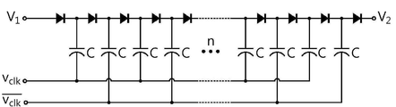
도 10은 다이오드들을 구비한 직렬 펌핑된 대칭 캐스케이드 멀티플레이어(series pumped symmetric cascade multiplier)를 나타내는 도면이다.
도 11은 다이오드들을 구비한 병렬 펌핑된 대칭 캐스케이드 멀티플레이어(parallel pumped symmetric cascade multiplier)를 나타내는 도면이다.
도 12는 충전 펌프(pump) 신호들을 나타내는 도면이다.
도 13은 스위치들을 구비한 2상(two-phase) 대칭 직렬 펌핑된 캐스케이드 멀티플레이어를 나타내는 도면이다.
도 14는 스위치들을 구비한 2상(two-phase) 대칭 병렬 펌핑된 캐스케이드 멀티플레이어를 나타내는 도면이다.
도 15는 반파장 버전들(half-wave versions)에 따른 네 가지의 다른 캐스케이드 멀티플레이어들을 나타내는 도면이다.
도 16은 주파수 기능으로서 스위치드 커패시터 컨버터(switched-capacitor converter)의 출력 임피던스를 나타내는 도면이다.
도 17은 전파가 단열적으로(adiabatically) 충전된 스위칭 네트워크를 구비한 도 1A에 도시한 DC-DC 컨버터의 특정 실시예를 나타내는 도면이다.
도 18은 위상 A 동안 도 17에 도시한 DC-DC 컨버터를 나타내는 도면이다.
도 19는 위상 B 동안 도 17에 도시한 DC-DC 컨버터를 나타내는 도면이다.
도 20은 4:1로 단열적으로 충전된 컨버터와 관련된 다양한 파형을 나타내는 도면이다.
도 21은 직렬로 연결된 단계들의 단열충전(adiabatic charging)을 나타내는 도면이다.
도 22는 도 21에 도시한 파워 컨버터의 특정 실시예를 나타내는 도면이다.
도 23은 재구성된 스위치드 커패시터 단계를 이용한 정류된 AC 전압을 나타내는 도면이다.
도 24는 AC-DC 파워 컨버터 아키텍처를 나타내는 도면이다.
도 25는 도 24에 도시한 AC-DC 컨버터의 특정 실시예를 나타내는 도면이다.
도 26은 AC 사이클의 양의 구간(positive portion) 동안 도 25에 도시한 AC-DC 컨버터를 나타내는 도면이다.
도 27은 AC 사이클의 음의 구간(negative portion) 동안 도 25에 도시한 AC-DC 컨버터를 나타내는 도면이다.
도 28은 역률개선회로(power-factor correction )을 구비한 AC-DC 컨버터 아키텍처를 나타내는 도면이다.
도 29 및 도 30은 도 1에 도시한 DC-DC 컨버터의 특정 실시예를 나타내는 도면이다.
도 31 및 도 32는 도 3에 도시한 DC-DC 컨버터의 특정 실시예를 나타내는 도면이다.
도 33 및 도 34는 도 2에 도시한 DC-DC 컨버터의 특정 실시예를 나타내는 도면이다.
도 35 및 도 36는 도 4에 도시한 DC-DC 컨버터의 특정 실시예를 나타내는 도면이다.1 is a diagram illustrating a DC-DC converter in which a regulating circuit and a switching network are separated.
1A is a diagram illustrating a bidirectional version of FIG. 1.
2-4 show a DC-DC converter with alternative configurations of regulating circuits and switching networks.
FIG. 5 is a diagram illustrating a specific embodiment of the power converter shown in FIG. 4.
FIG. 6 shows an embodiment of the invention with multiple regulating circuits. FIG.
7 is a diagram illustrating an RC circuit.
8 is a diagram illustrating a model of a switched capacitor DC-DC converter.
9A and 9B are diagrams illustrating a series-parallel SC converter operating in a charge phase and a discharge phase, respectively.
10 is a diagram illustrating a series pumped symmetric cascade multiplier with diodes.
FIG. 11 shows a parallel pumped symmetric cascade multiplier with diodes.
FIG. 12 is a diagram illustrating charge pump signals. FIG.
FIG. 13 is a diagram illustrating a two-phase symmetric series pumped cascade multiplayer with switches. FIG.
14 shows a two-phase symmetric parallel pumped cascade multiplayer with switches.
FIG. 15 is a diagram illustrating four different cascade multiplayers according to half-wave versions.
16 is a diagram showing the output impedance of a switched-capacitor converter as a frequency function.
FIG. 17 is a diagram illustrating a particular embodiment of the DC-DC converter shown in FIG. 1A with a switching network in which radio waves are adiabatically charged.
FIG. 18 shows the DC-DC converter shown in FIG. 17 during phase A. FIG.
FIG. 19 shows the DC-DC converter shown in FIG. 17 during phase B. FIG.
20 illustrates various waveforms associated with a 4: 1 adiabatically charged converter.
FIG. 21 is a diagram showing adiabatic charging of steps connected in series. FIG.
FIG. 22 is a diagram illustrating a specific embodiment of the power converter shown in FIG. 21.
FIG. 23 illustrates a rectified AC voltage using a reconfigured switched capacitor stage. FIG.
24 shows an AC-DC power converter architecture.
FIG. 25 is a diagram showing a specific embodiment of the AC-DC converter shown in FIG. 24.
FIG. 26 shows the AC-DC converter shown in FIG. 25 during the positive portion of the AC cycle.
FIG. 27 shows the AC-DC converter shown in FIG. 25 during the negative portion of the AC cycle.
FIG. 28 illustrates an AC-DC converter architecture with power-factor correction.
29 and 30 are diagrams showing particular embodiments of the DC-DC converter shown in FIG.
31 and 32 are diagrams showing specific embodiments of the DC-DC converter shown in FIG.
33 and 34 show specific embodiments of the DC-DC converter shown in FIG. 2.
35 and 36 illustrate a specific embodiment of the DC-DC converter shown in FIG. 4.
본 발명의 실시예에서는, 적어도, 다단 DC-DC 컨버터(multi-stage DC-DC converter) 내의 스위칭 네트워크 및 조절 회로는 본질적으로 모듈화되어 만들어 질 수 있으며, 여러 가지 다른 방법으로 매칭 및 혼합될 수 있다는 인식에 대한 부분에 최소한 의존하여 서술한다. 이는 이러한 컨버터들의 조립(assembly)에 대한 변형된 통합 전력 솔루션(TIPS

다음의 스위칭 네트워크들 및 조절 회로들의 실시예들과 관련되어 설명된 두 가지 기본 요소들이 있다. 동일 타입으로 구성된 요소가 직렬로 연결된 것으로 가정하면, 총 네 개의 기본적인 빌딩 블록들이 있다. 이들은 도 1 내지 도 4에 도시되어 있다. 본 발명의 실시예에서는 도 1 내지 도 4에 도시한 네 개의 기본 빌딩 블록들 중 적어도 하나를 포함하여 설명한다. There are two basic elements described in connection with the embodiments of the following switching networks and regulating circuits. Assuming elements of the same type are connected in series, there are a total of four basic building blocks. These are shown in Figures 1-4. An embodiment of the present invention includes at least one of the four basic building blocks shown in FIGS. 1 to 4.
추가적으로 본 발명의 실시예들은 다양한 속성을 갖는 DC-DC 컨버터들의 모듈 조립을 용이하게 하는 방식에 매칭되도록 입력들 및 출력들이 지속되는 동안, 여러 가지 다른 방식으로 "예시된(instantiated)" 조절 회로 16A와 스위칭 네트워크 12A를 가능하게 함에 의하여 DC-DC 컨버터들의 디자인을 위한 객체 지향형(object-oriented) 프로그래밍 컨셉들의 어플리케이션을 더 고려한다. In addition, embodiments of the present invention are “instantiated” regulating
다양한 실시예 내의 스위칭 네트워크 12A는 스위칭 커패시터 네트워크로서 예시된다. 보다 유용한 스위치드 커패시터 토폴로지들(topologies) 사이에 Ladder, Dickson, Series-Parallel, Fibonacci 및 Doubler 가 있으며, 모두 단열 충전 및 다상 네트워크로 구현될 수 있다. 특히 유용한 스위칭 커패시터 네트워크는 전파 캐스케이드 멀티플레이어(full-wave cascade multiplier)의 단열 충전 버전이다. 그러나, 단열 충전 버전들도 사용될 수 있다.
본 발명의 실시예에서, 단열적인 커패시터에 대한 충전이 변화하는 것은 비용량성(noncapacitive) 소자를 통해 전하를 패싱하는 것에 의한 변화로 커패시터에 전하량이 저장되는 것을 의미한다. 커패시터 전하 내의 양(positive)의 단열 변화는단열 충전으로 간주되는 반면, 커패시터 전하 내의 음(negative)의 단열 변화는 단열 방전되는 것으로 간주된다. 비용량성(noncapacitive) 소자들의 예들로는 인덕터들, 마그네틱 소자들, 레지스터들 및 그들의 조합들이 포함된다. In an embodiment of the present invention, changing the charge on the adiabatic capacitor means that the amount of charge is stored in the capacitor as a result of passing charge through the noncapacitive element. A positive adiabatic change in the capacitor charge is considered to be an insulating charge, while a negative adiabatic change in the capacitor charge is considered to be adiabatic discharge. Examples of noncapacitive elements include inductors, magnetic elements, resistors, and combinations thereof.
일부 케이스들에서, 커패시터는 일부 시간에서 단열적으로 충전될 수 있으며, 나머지 시간에서 비단열 방식으로 충전될 수 있다. 이러한 커패시터들은 단열적으로 충전되는 것으로 간주한다. 유사하게, 일부 실시예에서, 커패시터는 일부 시간에서 단열적으로 방전될 수 있으며, 나머지 시간에서 비단열 방식으로 방전될 수 있다. 이러한 커패시터들은 단열적으로 방전되는 것으로 간주한다. In some cases, the capacitor may be adiabaticly charged at some time and non-insulated at other times. These capacitors are considered to be adiabaticly charged. Similarly, in some embodiments, the capacitor may be adiabatic discharged at some time and may be discharged in a non-insulated manner at the remaining time. These capacitors are considered to be adiabatic.
비단열 충전은 단열적이지 않은 모든 충전을 포함하며, 비단열 방전은 단열적이지 않은 모든 방전을 포함한다. Non-insulated charges include all charges that are not adiabatic, and non-insulated discharges include all discharges that are not adiabatic.
본 발명의 실시예에서 사용되는 단열적으로 충전된 스위칭 네트워크는 단열적 충전 및 단열적 방전되는 적어도 하나의 커패시터를 구비한 스위칭 네트워크이다. 비단열적으로 충전된 스위칭 네트워크는 단열적으로 충전된 스위칭 네트워크가 아닌 스위칭 네트워크이다. An adiabaticly charged switching network used in an embodiment of the present invention is a switching network having at least one capacitor which is adiabaticly charged and adiabaticly discharged. A non-insulated switched network is a switching network rather than an adiabaticly charged switching network.
조절 회로 16A는 출력 전압을 조절할 수 있는 임의의 컨버터로서 예를 들 수 있다. 예를 들어, 벅 컨터버(buck converter)는 고효율 및 속도 때문에 유망한 후보이다. 다른 적합한 조절 회로 16A는 부스터 컨버터들(boost converters), 벅/부스터 컨버터들(buck/boost converters), 플라이 백 컨버터들(fly-back converters), Cuk 컨버터들(Cuk converters), 공진 컨버터들(resonant converters) 및 선형 레귤레이터들(linear regulators)을 포함한다.Regulating
본 발명의 실시예에서, 도 2에 도시한 바와 같이, 소스 전압 14은 스위칭 커패시터 네트워크로서 예를 든 제1 스위칭 네트워크 12A로 입력을 전달한다. 제1 스위칭 네트워크 12A의 출력은 조절 회로 16A(예를 들어, 벅(buck), 부스터(boost), 또는 벅/부스터 컨버터(buck/boost converter))에 제공되는 입력 전압보다 낮은 전압이다. 조절 회로 16A는 또 다른 스위칭 커패시터 네트워크인 제2 스위칭 네트워크 12B로 조절된 전압을 전달한다. 제2 스위칭 네트워크 12B의 고전압 출력은 부하 18A로 적용된다. In an embodiment of the invention, as shown in FIG. 2,
도 2에 도시한 바와 같이 본 발명의 실시예서는 에너지 흐름의 방향에 따라 소스 14를 조절하거나 또는 부하 18A를 조절하기 위해 구성될 수 있다. As shown in FIG. 2, embodiments of the present invention may be configured to adjust
또 다른 실시예에서, 도 3에서 도시한 바와 같이, 저전압 소스 14는 조절 회로 16A의 입력으로 연결되며, 출력은 보다 높은 DC 값으로 부스팅될 수 있도록 하기 위해 스위칭 네트워크 12A의 입력으로 전달된다. 그리고 나서, 스위칭 네트워크의 출력은 부하 18A로 전달된다. In another embodiment, as shown in FIG. 3,
도 3에 도시한 바와 같이 본 발명의 실시예에서는 에너지 흐름의 방향에 의존하여 소스 14 또는 부하 18A를 조절하는데 사용될 수 있다. As shown in FIG. 3, embodiments of the present invention can be used to adjust
다음 도 4를 참조하면, 컨버터 100의 또 다른 실시예서는 입력 102에 연결된 제1 조절 회로 300A 및 출력 104에 연결된 제2 조절 회로 300B를 포함한다. 제1 조절 회로 300A 와 제2 조절 회로 300B 사이에는 입력 202 및 출력 204을 구비한 스위칭 네트워크 200가 위치한다. 스위칭 네트워크는 스위치들 212에 의해 서로 연결된 충전 저장 소자들 210을 포함한다. 충전 저장 소자들 210들은 제1 그룹 206 및 제2 그룹 208로 구분된다.Referring next to FIG. 4, another embodiment of the
일부 실시예들에서, 스위칭 네트워크 200는 도 5에 도시한 바와 같이 양방향 스위칭 커패시터 네트워크일 수 있다. 도 5의 스위칭 커패시터 네트워크(switching capacitor network)는 제1 커패시터 20 및 제2 커패시터 22가 병렬로 구성되는 특징이 있다. 제1 스위치 24는 제1 커패시터 20 및 제2 커패시터 22 중의 하나를 제1 조절 회로 300A 에 선택적으로 연결하며, 제2 스위치 26는 제1 커패시터 20 및 제2 커패시터 22 중의 하나를 제2 조절 회로 300B 에 선택적으로 연결한다. 제1 스위치 24 및 제2 스위치 26 모두 고주파에서 동작될 수 있으며, 제1 커패시터 20 및 제2 커패시터 22의 단열 충전 및 방전을 가능하게 할 수 있다. In some embodiments, the
도 5에 도시한 바와 같이 특정 실시예에서는 2상 스위칭 네트워크(two-phase switching network) 200를 포함한다. 그러나, 스위칭 네트워크들의 다른 타입들이 대신 사용될 수 도 있다.As shown in FIG. 5, certain embodiments include a two-
또 다른 실시예에서, 도 6에 도시한 바와 같이, 다중 조절 회로들 16A, 16B, 16C은 다중 부하들 18A-18C을 구동시키기 위해 제1 스위칭 네트워크 12A의 출력을 전달할 수 있다. 부하들 중의 하나인 18C를 위하여, 제2 스위칭 네트워크 12B는 부하 18C 및 이에 대응하는 조절 회로 16C 사이에서 제공되며 도 2에 도시한 것과 유사한 경로를 생성한다. 도 6은 DC-DC 컨버터 구성에 유연성을 제공하도록 요소들을 매칭 및 혼합하는 기능이 용이한 조절 회로들 및 스위칭 네트워크들의 모듈형 구성 방법의 예를 제공한다. In another embodiment, as shown in FIG. 6, multiple regulating
스위치드 커패시터 (SC) DC-DC 파워 컨버터는 스위치들 및 커패시터들의 네트워크를 포함한다. 이러한 스위치들을 이용하여 다른 토폴로지 단계들을 통해 네트워크를 순환시킴에 따라, SC 네트워크의 입력으로부터 출력으로 에너지를 전달할 수 있다. "충전 펌프"로 알려진 일부 컨버터들은 플레시(FLASH) 및 다른 재프로그램 가능한 메모리의 고전압 생성을 위해 사용될 수 있다. Switched Capacitor (SC) DC-DC power converters include a network of switches and capacitors. These switches can be used to transfer energy from the input to the output of the SC network by cycling the network through different topology steps. Some converters known as "charge pumps" can be used for high voltage generation of flash and other reprogrammable memories.
도 7은 임의의 전압 Vc(0)로 초기 충전된 커패시터 C를 나타내는 도면이다. 스위치 S 는 t = 0에서 닫힌다. 이 순간, 전류의 브리프 서지(brief surge)는 커패시터 C가 Vin의 최종 전압으로 충전됨으로써 흐른다. 충전률은 최종 전압의 허수(lie) 내에 전압이 증가하거나 또는 감소하는데 걸리는 시간을 나타내는 시간 상수 


커패시터를 충전하 는 동안 발생하는 에너지 손실은 레지스터 R에서 소모되는 에너지를 계산함으로써 발견될 수 있다. The energy loss that occurs while charging the capacitor can be found by calculating the energy dissipated in resistor R.

방정식은 ic(t)에 대한 표현들을 방정식(1.2)으로부터 방정식(1.3)으로 대체하고, 그리고 나서 적분(integral)을 계산함으로써 더욱 단순화될 수 있다. The equation can be further simplified by replacing the expressions for i c (t) from equation (1.2) to equation (1.3), and then calculating the integral.
방정식은 ic(t )에 대한 표현들을 방정식(1.2)으로부터 방정식(1.3)으로 대체하고, 그리고 나서 적분(integral)을 계산함으 로써 더욱 단순화될 수 있다. The equation can be further simplified by replacing the expressions for i c (t) with equation (1.3) from equation (1.2) and then computing the integral.

만일 트랜지스터들이 세틀(settle, 예 를 들어, t-oo)이 허락된다면, 커패시터 충전 시 초래되는 총 에너지 손실은 저항값 R에 독립적이다. 이러 한 경우, 에너지 손실량은 아래와 같다. If the transistors are allowed to settle (eg t-oo), the total energy loss incurred when charging the capacitor is independent of the resistance value R. In this case, the energy loss is as follows.

스위치드 커패시터 컨버터는, 도 8에 도시한 바와 같이, 에너지 변환 커패시터들의 방전 또는 충전 시 초래될 수 있는 전력 손실에 대한 것으로 간주되는 유한 출력 저항(finite output resis tance) Ro을 구비한, 도 8에 도시한 바와 같은, 이상적인 변압기로서 모델링 될 수 있다. 이러한 손실은 커 패시터들의 등가 직렬 저항 및 MOSFETs의 ON 저항에서 일반적으로 소모된다.The switched capacitor converter is shown in FIG. 8, as shown in FIG. 8, with a finite output resistance Ro, which is considered for power loss that may result from the discharge or charging of the energy conversion capacitors. As one can, it can be modeled as an ideal transformer. This loss is typically consumed by the equivalent series resistance of the capacitors and the ON resistance of the MOSFETs.
스위치드 커패시터 컨버터 의 출력 전압은 다음과 같이 주어진다.The output voltage of the switched capacitor converter is given by

스위치드 커패시터 컨버터들의 동작을 간략화할 수 있으며, R0를 쉽게 찾을 수 있는 두 가지 제한적인 경우 들이 있다. 이들은 "저속스위칭 제한(slowswitching limit)" 및 "고속스위칭 제한(fast-switching limit)"으 로 불리운다. The operation of switched capacitor converters can be simplified and there are two limited cases where R0 can be easily found. These are called "slowswitching limits" and "fast-switching limits".
고속스위칭 제한(
저속스위칭 제한에서, 스위칭 기간 Tsw 는 에너지 변환 커패시터들의 RC 시간 상수 T보다 길다. 이러한 상황에서, 전체적인 에너지는 커패시터들 및 스위치들의 저항에 상관없이 손실된다. 이러한 전체적인 에너지 손실은 충전 및 방전 전류의 RMS(root mean square)가 RC 시간 상수의 함수이기 때문에 부분적으로 발생된다. 만일 충전 경로(charging path)의 유효 저 항 Reff 이 감소되면(예를 들어, RC가 감소되면), RMS 전류는 증가하며, 총 충전 에너지 손실(
스위칭 커패시터 네트워크가 공통 접지, 큰 변압비(transformation ratio), 낮은 스위치 강도(switch stress), 낮은 DC 커패시터 전압 및 낮은 출력 저항을 구비하는 것은 바람직하다. 보다 유용한 토폴로지는 Ladder, Dickson, Series-Parallel, Fibonacci 및 Doubler 가운데 있다. It is desirable for the switching capacitor network to have a common ground, large transformation ratio, low switch stress, low DC capacitor voltage and low output resistance. More useful topologies are among Ladder, Dickson, Series-Parallel, Fibonacci, and Doubler.
유용한 컨버터의 하나는 직병렬 스위치드 커패시터 컨버터(series-para llel switched capacitor)이다. 도 9A 및 도 9B는 충전 위상 및 방전 위상이 각각 2:1 인 직병렬 스위치드 커패시터 컨버터를 나타내는 도면이다. 충전 위상 동안, 커패시터들은 직렬이 된다. 방전 위상 동안, 커패시 터들은 병렬이 된다. 충전 위상에서 커패시터 전압들 VC1 및 VC2는 V1 에 더해지는 반면, 방전 위상에서 VC1 및 VC2는 V2와 같아 진다. 이때, V2 = V1/2을 의미한다. One useful converter is a series-parallel switched capacitor. 9A and 9B are diagrams illustrating a series-parallel switched capacitor converter having a charge phase and a discharge phase of 2: 1, respectively. During the charging phase, the capacitors are in series. During the discharge phase, the capacitors are in parallel. In the charging phase, the capacitor voltages V C1 and V C2 are added to V 1 , while in the discharge phase V C1 And V C2 are equal to V 2 . At this time, V 2 = V 1/2 .
다른 유용한 토폴로지들은 도 10 및 도 11에 도시한 캐스케이드 멀티플레이어 토폴로지들(cascade multiplier topologies)이다. 양쪽 충전 펌프들 에서, 소스는 V1에 위치해 있으며, 부하는 V2에 위치해 있다. 이러한 타입들의 충전 펌프들에서, 충전의 패킷들은 커플링 커패시터들(coupling capacitors)이 성공적으로 충전 및 방전됨으 로써 다이오드 체인을 따라 펌핑된다. 도 12에 도시한 바에 따라, 진폭 vpump 를 포함하는 클 록 신호 Vclk 및 
초기 충전이 출력으로 도달하기 위해서는 n 클록 사이클들이 소요된다. 마지막 펌프 커패시 터에 대한 충전은 처음 펌프 커패시터에 대한 충전보다 n 배 더 걸리므로 컨버터들에 대한 출력 전압 V 2는 양쪽 펌핑 구성들에서 
앞선 토폴로지들 이 전압을 승압하는데 적당하지만, 소스와 부하의 위치를 바꿈으로써 전압을 감압하는데 사용할 수도 있다. 이러한 경우, 다이오드들은 MOSFETs 및 BJTs와 같은 조절 스위치들로 교체될 수 있다. While the previous topologies are suitable for boosting voltage, they can also be used to reduce the voltage by changing the source and load positions. In this case, the diodes can be replaced with regulating switches such as MOSFETs and BJTs.
앞서 말한 캐스 케이드 멀티플레이어들은 충전이 클록 신호의 1 상(one phase) 동안 전송되어지는 반파 멀티플레이어들(hal f-wave multipliers)이다. 이것은 입력 전류의 불연속성을 야기한다. 이러한 캐스케이드 멀티플레이어들은 모두 두 개의 반파 멀티플레이어들을 병렬로 연결하거나 180도의 위상차의 멀티플레이어들을 실행시킴으로써 전파 멀티플레이어들(full-wave multipliers)로 변환시킬 수 있다. 도 13은 전파 대칭 직렬 펌핑된 캐스케이 드 멀티플레이어(full-wave symmetric series pumped cascade multiplier) 버전을 나타내는 도면인 반면, 도 14는 전파 대칭 병렬 펌핑된 캐스케이드 멀티플레이어(full-wave symmetric parallel pumped cascade multi plier) 버전을 나타내는 도면이다. 반파 멀티플레이어(half-multiplier)의 다이오드들과 다르게, 도 13 및 도 14의 스위치들은 양방향성을 갖는다. 이러한 캐스케이드 멀티플레이어들 모두의 결과로서, 전력은 소스로 부터 부하까지 흐르거나 또는 부하로부터 소스로 흐를 수 있다. 비대칭 멀티플레이어들은 전파 멀티플레이어 들로 변환될 수 있다. The aforementioned cascade multiplayers are half f-wave multipliers in which charge is transmitted during one phase of the clock signal. This causes discontinuities in the input current. These cascade multiplayers can all be converted to full-wave multipliers by connecting two half-wave multiplayers in parallel or by running 180 degrees of phase difference multiplayers. FIG. 13 shows a full-wave symmetric series pumped cascade multiplier version, while FIG. 14 shows a full-wave symmetric parallel pumped cascade multiplayer. plier). Unlike the diodes of half-multiplier, the switches of FIGS. 13 and 14 are bidirectional. As a result of all of these cascade multiplayers, power may flow from source to load or from load to source. Asymmetric multiplayers can be converted to full-wave multiplayers.
도 15는 해당하는 반파 버전들에 따른 전파 멀티플레이어들의 네 가지 다른 전 압 증가 버전들이다. 뿐만 아니라, 병렬로 N 위상을 결합가능하며, 출력 전압 리플(output voltage ripple) 을 감소시키고, 출력 전력 처리 능력을 증가시키기 위해 180 degrees/N 위상차로 동작시킬 수 있다. 15 is four different voltage increasing versions of propagating multiplayer according to corresponding half-wave versions. In addition, N phases can be combined in parallel, and can be operated with 180 degrees / N phase difference to reduce output voltage ripple and increase output power processing capability.
도 1 내지 4에 도시한 모듈형 아키텍쳐의 기본 빌딩 블록들은 독립적인 개체들(entities) 또는 커플링된 개 체들(entities)로서 연결될 수 있다. 이러한 상황의 스위칭 네트워들 및 조절회로들은 밀접하게 결합되어 있 으며, 단열 충전을 통한 스위칭 네트워크들의 전체적인 에너지 손실 메커니즘(mechanism)을 줄이거나 또는 막을 수 있다. 스위칭 네트워크의 커패시터들의 충전 및 방전을 제어하기 위해 일반적으로 제어 회로(regul ating circuit)를 사용한다. 뿐만 아니라, 조절 회로 및 전체 컨버터의 출력 전압은 외부 자극에 응답하여 조절될 수 있다. 출력 전압을 조절하는접근 방법은 자기 기억 소자(magnetic storage element)의 평균 DC 전 류를 제어하는 것이다. The basic building blocks of the modular architecture shown in FIGS. 1 to 4 may be connected as independent entities or coupled entities. The switching networks and regulating circuits in this situation are tightly coupled and can reduce or prevent the overall energy loss mechanism of the switching networks via adiabatic charging. Generally, a regul ating circuit is used to control the charging and discharging of the capacitors of the switching network. In addition, the regulating circuit and the output voltage of the entire converter can be regulated in response to an external stimulus. An approach to regulating the output voltage is to control the average DC current of the magnetic storage element.
조절 회로의 바람직한 특징은 스위칭 네트워크의 커패시터들를 통해 흐르는 RMS 전류를 제한하는 것이다. 이를 위해, 조절 회로는 저항 또는 자기 저장 소자들(magnetic storage elements) 을 사용한다. 불행히도, 저항 소자들은 전력을 소비하므로 활용을 적게 하는 것이 바람직하다. 따라서, 본 발명의 실시예에서는 조절 회로 내의 자기 저장 소자 및 스위치들의 조합에 의존하여 설명한다. 조절 회로는 평균 DC 전류를 구비한 조절 회로의 자기 저장 소자를 통해 흐르는 커패시터 전류에 의하여 RMS 전류를 제한 한다. 조절 회로의 스위치들은 자기 저장 소자를 통해 흐르는 평균 DC 전류를 유지하기 위한 것으로서 동작 될 수 있다. A desirable feature of the regulating circuit is to limit the RMS current flowing through the capacitors of the switching network. For this purpose, the regulating circuit uses resistors or magnetic storage elements. Unfortunately, resistive devices consume power, so it is desirable to use less. Thus, embodiments of the present invention are described depending on the combination of magnetic storage elements and switches in the regulating circuit. The regulating circuit limits the RMS current by the capacitor current flowing through the magnetic storage element of the regulating circuit with an average DC current. The switches of the regulating circuit can be operated as to maintain the average DC current flowing through the magnetic storage element.
조절 회로는 스위칭 네스워크 내의 적어도 하나의 커패시터의 RMS 충전 전류 및 RMS 방전 전류 모두를 제한한다. 단일 조절 회로는 싱킹(sinking) 및/또는 소싱(sourcing) 전류에 의해 스위칭 네트워 크의 입력 또는 출력 전류를 제한한다. 도 1 내지 도 4에 도시한 바와 같이 네 가지 기본 구성들이 있다. 도 1에서 전력이 소스로부터 부하로 흐르는 것으로 가정하면, 조절 회로 16A는 스위칭 네트워크 12A의 충전 및 방전 전류 모두를 싱킹(sinking) 할 수 있다. 도 3에서 조절 회로 16A는 스위칭 네트워크 12A의 충전 및 방 전 전류 모두를 소싱(sourcing) 할 수 있다. 도 4에서, 조절 회로 300A는 스위칭 네트워크 200의 충전 전류 를 소싱할 수 있으며, 조절 회로 300 B는 같은 스위칭 네트워크 200의 충전 전류를 싱킹할 수 있으며, 그 반 대의 경우도 마찬가지 이다. 도 2에서, 조절 회로 16A는 스위칭 네트워크 12B의 충전 및 방전 전류 모두를 소싱할 수 있는 반면, 또한 스위칭 네트워크 12A의 충전 및 방전 전류 모두를 싱킹할 수 있다. 뿐만 아니라 , 스위칭 네트워크들 및 조절 회로들 모두가 양방향으로 전력 흐름이 가능하다면, 양방향의 전력 흐름이 가 능(소스에서 부하 및 부하에서 소스)해진다. The regulating circuit limits both the RMS charge current and RMS discharge current of at least one capacitor in the switching scheme. A single regulating circuit limits the input or output current of the switching network by sinking and / or sourcing current. There are four basic configurations as shown in FIGS. Assuming power flows from source to load in FIG. 1, regulating
한 실시예에서는 적어도 부분적인 단열 충전되는 전파 캐 스케이드 멀티플레이어들에 의존한다. 캐스케이드 멀티플레이어들은 우수한 고속 스위칭 제한 임피던스, 전 압 스케일 향상이 용이성 및 낮은 스위치 강도(switch stress) 때문에 스위칭 네트워크로 선호된다. In one embodiment, it depends on at least partially adiabaticly charged propagation cascade multiplayers. Cascade multiplayers are preferred for switching networks because of their high fast switching limit impedance, ease of voltage scale enhancement, and low switch stress.
캐스케이드 멀티플레이어들에서, 커플링 커패시터들은 일반적으로 클록 전압 소스 Vclk & 


조건을 동일하게 하여, 단열적으로 충전된 스위치드 커패시터 컨버터는 종래 충 전된 스위치드 커패시터 컨버터보다 스위칭 주파수를 훨씬 많이 감소시켜 동작할 수 있지만, 보다 더 높은 효율성을 갖도록 할 수도 있다. 반대로, 단열적으로 충전된 스위치드 커패시터 컨버터는 종래 충전된 스위치 드 커패시터 컨버터와 같은 효율성을 가지며 같은 주파수에서 동작하지만, 예를 들어 4배에서 10배 사이로 훨씬 더 작은 작은 커플링 커패시터들을 구비해야 한다.With the same conditions, adiabaticly charged switched capacitor converters can operate with much lower switching frequency than conventionally charged switched capacitor converters, but may also have higher efficiency. Conversely, adiabaticly charged switched capacitor converters have the same efficiency as conventionally charged switched capacitor converters and operate at the same frequency but must have smaller coupling capacitors that are much smaller, for example between 4 and 10 times.
도 17은 도 1A에 도시한 아키텍처를 구비한 감압 컨버터(step-down converter) 구성을 나타내는 도면이다. 그러나, 이러한 실시예에서는, 스위칭 네트워크 (12A)는 조절 회로 16A를 이용하여 단열적으로 충전된다. 클록 전류 소스들 iclk & 
구동에서, 1로 표시된 스위치들이 닫히면(close) 커패시터들 C 4, C5 및 C6 이 충전되며, 반면 커패시터들 C1, C 2 및 C3 은 방전된다. 유사하게, 2로 표시된 스위치들이 닫히면 상호 보완적인 효과를 갖는다. 제1 토폴로지 단계(위상 A)는 1로 표시된 모든 스위치들이 닫히며, 2로 표시된 모든 스위치들은 개 방(open)된 18과 같다. 유사하게, 제2 토폴로지 단계(위상 B)는 2로 표시된 모든 스위치들이 닫히며, 1로 표시된 모든 스위치들이 개방된 도 19와 같다. 본 발명의 실시예에서, 조절 회로 16A는 각 커패시터의 RMS 충전 및 방전 전류를 제한한다. 예를 들면, 커패시터 C3 은 위상 A 동안 조절 회로 16A의 필터 인덕터를 통해 방전되는 반면, 커패시터 C3 은 위상 B 동안 조절 회로 16A의 필터 인덕터를 통해 충전되어 명확한 단열 개념을 보여준다. 뿐만 아니라, 모든 능동 구성들이 스위치들로 구현되어 컨버터는 양방향으로 전력을 처리할 수 있다. In operation, when the switches marked 1 close the capacitors C 4 , C 5 And C 6 are charged, while capacitors C 1 , C 2 and C 3 are discharged. Similarly, the switches marked 2 have a complementary effect. In the first topology phase (phase A), all switches marked 1 are closed and all switches marked 2 are equal to 18 opened. Similarly, the second topology phase (phase B) is the same as in FIG. 19 where all switches marked 2 are closed and all switches marked 1 are open. In an embodiment of the invention, regulating
대표적인 노드 전압들 및 전류들은 도 20에 도시한 바와 같다. 두 개의 도시된 전류들(IP1 및 IP2)의 상승 및 하강 에지들에는 소량의 왜곡이 있으나, 전반적인 부분에서, 전류들은180도의 위상차가 나는 두 클록들과 유사하다. 일반적으로, 단열 충전은 적어도 스위치 스택의 한 끝단이 정전용량(capacitance)을 로드(load)하지 않아야만 캐스케이드 멀티플레이어 내에서 발생되므로, 본 발명의 실시예의 경우에서는, 노드 Vx는 조절 회로 16A에 의해 감압된다. Representative node voltages and currents are as shown in FIG. 20. There is a small amount of distortion at the rising and falling edges of the two illustrated currents I P1 and I P2 , but in general, the currents are similar to two clocks that are 180 degrees out of phase. In general, adiabatic charging occurs in cascade multiplayer at least when one end of the switch stack does not load capacitance, so in the case of an embodiment of the present invention, node Vx is controlled by regulating
도 1 내지 도 4에 도시한 기본 빌딩 블록들을 구비한 모듈형 아키텍처는 고전압 DC, AC-DC, 벅 부 스터(buck-boost) 및 다중 출력 전압들(multiple output voltages)과 같은 응용들의 범위를 더 넓게 커버하 기 위해 확장될 수 있다. 이러한 각 응용들은 분리된 변환 및 조절 기능들을 포함한다. 아키텍처의 확장은 또한 단열 충전된 스위치드 커패시터 컨버터들을 통합할 수 있다.The modular architecture with the basic building blocks shown in FIGS. 1-4 further extends the range of applications such as high voltage DC, AC-DC, buck-boost and multiple output voltages. It can be extended to cover wider. Each of these applications includes separate conversion and adjustment functions. Expansion of the architecture can also incorporate adiabatic charged switched capacitor converters.
복수의 스위치드 커패시터 컨버터들에 서, 커패시터들 및 스위치들의 개수는 변압비(transformation ratio)에 선형적으로 증가한다. 게다가, 변압비가 커지게 되면 복수의 커패시터들 및 스위치들이 필요하게 된다. 대신, 큰 변압비는 도 21에 도시된 낮은 게인 단계들을 복수로 직렬 연결함으로써 달성될 수 있다. 전체 스위치 커패시터 스택(Vin/V x)의 변압비는 다음과 같다:In a plurality of switched capacitor converters, the number of capacitors and switches increases linearly with the transformation ratio. In addition, a large transformer ratio requires a plurality of capacitors and switches. Instead, a large transformer ratio can be achieved by connecting a plurality of low gain steps shown in FIG. 21 in series. The transformer ratio of the entire switch capacitor stack (V in / V x ) is:

구성들이 적재되는 직렬의 가장 단점은 앞 단계들에서 전압 강도(voltageThe most disadvantage of the series in which the configurations are loaded is the voltage strength in the preceding steps
stresses)가 뒤 단계들 보다 훨씬 높은 것이다. 이는 일반적으로 다른 전압 등급들(ratings) 및 크기들(siz es)을 구비한 단계들을 요구할 것이다. stresses) are much higher than later steps. This will generally require steps with different voltage ratings and magnitudes.
전술한 직렬 연결된 스위치드 네트워크의 단열 충전은 그 다음 스위칭 네트워크가 전술한 단계의 충전 및 방전 전류로 제어되는 경우에만 발생된다 . 이에 따라, 선행 단계들에서 전파 스위치드 커패시터 컨버터들을 사용하거나 또는 입력 필터들에 기초한 자성(magnetic)을 갖는 단일 위상 직병렬 스위치드 커패시터 컨버터들(singlephase series-parallel switch ed-capacitor converters)과 같은 스위치드 커패시터 단계들을 선행하는 것이 바람직하다. The adiabatic charging of the series-connected switched network described above is then generated only if the switching network is controlled by the charging and discharging currents of the above-mentioned steps. Thus, switched capacitor stages, such as single phase series-parallel switch ed-capacitor converters, using electromagnetically switched capacitor converters in the preceding stages or having a magnetic based on input filters. It is preferable to precede them.
도 22는 도 21에 도시한 아키텍처를 구비한 두 개의 직렬 연결된 스위칭 네트워크들 구성을 구비한 컨버터를 나타내는 도면이다. 스위칭 네트워크들 12A 및 12D는 2상 캐스케이드 멀티플레이어들(two-phase cascade multipliers )이다. 동작에 있어서, 1 및 2로 표시된 스위치들 은 항상 상호 보완적인 단계들(complementary states)이며 , 7 및 8로 표시된 스위치들은 항상 상호 보완적인 단계들이다. 게다가, 제1 전환 상태(switched-state)에서 , "1"로 표시된 모든 스위치들은 개방(open) 되며, "2"로 표시된 모든 스위치들은 닫히게(close) 된다. 제2 전환 상태(switched-state)에서, "1"로 표시된 모든 스위치들은 닫히게 되며, "2"로 표시된 모든 스위치들 은 개방된다. 본 발명의 실시예에서, 1로 표시된 닫힌 스위치들은 커패시터들 Cl , C 2, C3을 충전시키는 반면 C4, C5, C6은 방전 시키며, 2로 표시된 닫힌 스위치들은 상호 보완적인 효과를 갖는다. 또한, 7로 표시된 닫힌 스위치들은 커패 시터들 C7 , C8, C9를 충전시키는 반면 C10, C11, C12는 방전시키며, 8로 표시된 닫힌 스위치들은 상호 보완적인 효과를 갖 는다.FIG. 22 is a diagram illustrating a converter with two serially connected switching networks having the architecture shown in FIG. 21.
파워 컨버터는 32:1의 전체 감압(step-down)을 제공하며, 조절 회로 16A는 일반적인 2:1 의 감압 비율을 구비한 벅 컨버터(buck converter)이다. 뿐만 아니라, 만일 입력 전압이 32V이고 출력 전압이 1 V라 면, 제1 스위칭 네트워크 12A 내의 스위치들이 8볼트(volt)를 차단하는 동안 제2 스위칭 네트워크 12D의 스 위치들은 2볼트(volt)를 차단할 것이다. The power converter provides a 32: 1 total step-down, and the regulating
도 1 내지 도 4에 도시한 기본 빌딩 블록들을 구비한 모듈형 아키텍처들은 또한 AC 입력 전압들을 처리하기 위해 구성될 수 있다. 스위치드 커패시터 컨버터들의 주요 특 성 중의 하나는 스위치드 커패시터 네트워크를 재구성함으로써 큰 입력 범위 에서도 효율적으로 동작할 수 있는 능력이다. 만일 AC 장벽 전압(예를 들어, 60 Hz & 120 VRMS)이 저속으로 흐르는 DC 전압 으로서 간주되면, 전단부(front-end)의 스위치드 커패시터 단계는 상대적으로 안정된 DC 전압으로 시변환 입 력 전압(time-varying input voltage)을 전개할 수 있다. Modular architectures with the basic building blocks shown in FIGS. 1-4 can also be configured to handle AC input voltages. One of the key characteristics of switched capacitor converters is their ability to operate efficiently over large input ranges by reconfiguring the switched capacitor network. If the AC barrier voltage (e.g. 60 Hz & 120 V RMS ) is regarded as a slow flowing DC voltage, then the front-end switched capacitor stage is a relatively stable DC voltage, time-varying input voltage).
전개된 DC 전압을 구비한 단일 60 Hz 사이 클에 겹친 120 V RMS AC 파형의 다이어그램은 도 23에 도시한 바와 같다. AC 스위칭 네 트워크는 반전 단계에 따라 처리된 다른 구성들(1/3, 1/2, 1/1)을 포함한다. 이는 또한 60V 이하의 DC 전압 을 유지하기 위해 설계되었다. 일단 AC 전압이 전개되면, 마지막 출력 전압을 생성하기 위한 조절 회로 16A 의 동작은 도 24와 같다. 더 나은 전압 상태를 위해 AC 스위칭 네트워크 13A 및 조절 회로 16A 사이에 또 다 른 스위칭 네트워크 16A가 위치할 필요가 있다. 만일 이러한 경우, AC 스위칭 네트워크 13A는 특정한 목적 스위칭 네트워크 12A이므로 직렬 연결된 단계들에 대한 규칙들이 적용된다. 120 V RMS superimposed on a single 60 Hz cycle with developed DC voltage A diagram of the AC waveform is as shown in FIG. The AC switching network includes other configurations (1/3, 1/2, 1/1) processed according to the inversion step. It is also designed to maintain a DC voltage below 60V. Once the AC voltage has developed, the operation of regulating
도 25는 도 24에 도시한 아 키텍처에 해당하는 AC-DC 컨버터를 나타내는 도면이다. 본 발명의 실시예에서, AC 스위칭 네트워크 13A는 세 가지 별개의 전환비율(1/3, 1/2, 1/1)을 구비한 가변구조형 2 상 감압 캐스케이드 멀티플레이어(two-phase step-down cascade multiplier)에 뒤이은 동기식 AC 브릿지(AC bridge)인 반면 조절 회로 16A는 동기식 벅 컨버터(buckconverter)이다. 구동면에서, 7 및 8로 표시된 스위치들은 항상 상호 보완적 단계들이다. AC 사 이클(0 to 


7 및 8로 표시된 스위치들 에 의해 제공되는 인버팅 기능 이외에, 1A-1E로 표시된 스위치들 및 2A-2E로 표시된 스위치들은 1/3, 1/2 및 1의 세 가지 별개의 전환비율(conversion ratios)을 제 공하기 위해 테이블1에 도시한 것처럼 선택적으로 닫히거나 개방된다. In addition to the inverting function provided by the switches labeled 7 and 8, the switches labeled 1A-1E and the switches labeled 2A-2E provide three separate conversion ratios: 1/3, 1/2, and 1. It is optionally closed or opened as shown in Table 1 to provide).

AC 스위칭 네트워크 13A는 디지털 클록 신호 CLK를 전달한다. 또한, 두번째 신호 CLKB는 단순하게 CLK(예를 들어, CLK 가 로우(low)일 때 하이(high)가되고, CLK가 하이(high)일 때 로우(low)가 된다 )의 보수(complement)로 생 성되거나, 또는 종래에 알려진 것처럼 비중첩 보수(non-overlapping complement)로서 생성되어 질 수 있다. 테이블 1의 첫번째 열에 따라 설정된 스위칭 패턴들을 갖는 AC 스위칭 네트워크 13A는 1/3의 감압 비율(ste pdown ratio)을 제공한다. 테이블 1의 두번째 열에 따라 설정된 스위칭 패턴들을 갖는 AC 스위칭 네트워크 13A는 1/2의 감압 비율을 제공한다. 테이블 1의 첫번째 열에 따라 설정된 스위칭 패턴들을 갖는 AC 스위칭 네트워크 13A는 1의 감압 비율을 제공한다.
장벽이 포함된 대부분의 파워 서플라이들은 소정의 역률(po wer factor) 사양을 충족시킨다. 역률은 피상 전력(apparent power)으로 흐르는 실제 전력의 비율로 정의된 0과 1 사이의 무차원의 수(dimensionless number)이다. 고조파 전류(harmonic current) 제어 및 역률 증가를 위한 공통 방법은 도 28에 도시한 바와 같은, 능동 PFC(active power factor corrector)를 사용하는 것이다 . 역률개선회로(power-factor correction circuit) 17A는 입력 전류가 선간 전압(line voltage)과 같은 위상 이 되는 원인이며, 또한 무효전력소비(reactive power consumption)가 제로(0)가 되는 원인이다. Most power supplies with barriers meet certain power factor specifications. Power factor is a dimensionless number between 0 and 1 defined as the ratio of actual power flowing to apparent power. A common method for harmonic current control and power factor increase is to use an active power factor corrector (PFC), as shown in FIG. The power-
도 29 내지 도 36은 도 1 내지 도 4에 도시한 아키텍처 다이어그램들에 따른 파워 컨버터들의 구체적인 실시예를 나타내는 도면이다. 본 발명의 실시예에 따른 조절 회로 및 다중 조절 회로들은 각 스위칭 네트워크 내 적어도 하나의 커패시터의 RMS 충전 전류 및 RMS 방전 전류를 제한할 수 있으므로 이러한 스위칭 네트워크 들은 모두 단열적으로 충전되는 스위칭 네트워크들이다. 그러나, 비커플링 커패시터들(decoupling capacito rs) 9A 또는 9B가 존재하면, RMS 충전 및 방전 전류를 제한하는 조절 회로의 기능은 줄어들 수 있다. 커패시 터들 9A 또는 9B는 선택적이며, 아주 일정한 출력 전압을 유지하기 위해 커패시터 Co를 사용한다. 뿐만 아니 라, 용이함을 위해, 각 실시예의 스위칭 네트워크는 단일 전환 비율(conversion ratio)을 구비한다. 그러나 , 복수의 별개 전환 비율로 전력 변환을 제공하는 재구성 스위칭 네트워크들이 대신 사용될 수 도 있다. 29 through 36 illustrate specific embodiments of power converters according to the architecture diagrams illustrated in FIGS. 1 through 4. Since the regulating circuit and the multiple regulating circuits according to the embodiment of the present invention can limit the RMS charging current and the RMS discharge current of at least one capacitor in each switching network, these switching networks are all thermally charged switching networks. However, if there are
구동면에서, 1 및 2로 표시된 스위치들은 항상 상호 보완적인 상태이다. 따라서, 제1 전환 상태는, "1"로 표 시된 모든 스위치들이 개방되고, "2"로 표시된 스위치들이 모두 닫히게 된다. 제2 전환 상태는, "1"로 표시 된 모든 스위치들은 닫히게 되고, "2"로 표시된 모든 스위치들은 모두 개방된다. 유사하게, "3" 및 "4"로 표 시된 스위치들은 상호 보완적인 상태에 있으며, "5" 및 "6"으로 표시된 스위치들은 상호 보완적인 상태에 있으며, "7" 및 "8"로 표시된 스위치들은 상호 보완적인 상태에 있다. 전형적으로, 조절 회로들은 스위칭 네 트워크들보다 더 높은 스위칭 주파수들로 구동된다. 그러나, 스위칭 네트워크들 및 조절 회로들 사이에 스위 칭 주파수들은 요구되지 않는다. In driving terms, the switches labeled 1 and 2 are always complementary. Thus, in the first switching state, all switches marked as "1" are opened and all switches marked as "2" are closed. In the second switching state, all switches marked "1" are closed and all switches marked "2" are all open. Similarly, the switches labeled "3" and "4" are in a complementary state, and the switches labeled "5" and "6" are in a complementary state, and the switches labeled "7" and "8". Are in a complementary state. Typically, the regulating circuits are driven at higher switching frequencies than the switching networks. However, no switching frequencies are required between the switching networks and the regulating circuits.
도 29는 도 1에 도시한 아키텍처에 해당하는 승압 컨버터(step-up co nverter)에 대한 도면이다. 본 발명의 실시예에서, 스위칭 네트워크 12A는 1:3의 전환 비율을 갖는 2 상 승 압 캐스케이드 멀티플레이어(two-phase step-up cascade multiplier)인 반면, 조절 회로 16A는 2 상 부스터 컨버터(two-phase boost converter)이다. 구동면에서, 1로 표시된 닫힌 스위치들 및 2로 표시된 개방 스위치 들은 커패시터들 C3 및 C4를 충전시키는 반면 C1 및 C2 는 방전시킨다. 반대로, 1로 표시된 개방 스위치들 및 2로 표시된 닫힌 스위치들은 커패시터들 C1 및 C2를 충전시키는 반면 C3 및 C4는 방전시킨다.FIG. 29 is a diagram of a step-up converter corresponding to the architecture shown in FIG. 1. In an embodiment of the invention, the
도 30는 도 1A에 도시한 아키텍처에 해당하는 양방향 감압 컨버터(bidirectional step-down converter)를 나타내는 도면 이다. 본 발명의 실시예에서, 스위칭 네트워크 12A는 4:1의 전환 비율을 갖는 2상 감압 캐스케이드 멀티플레 이어(twophase step-down cascade multiplier)인 반면, 조절 회로 16A는 동기식 벅 컨버터(synchronous bu ck converter)이다. 구동면에서, 1로 표시된 닫힌 스위치들 및 2로 표시된 개방 스위치들은 커패시터들 C 1, C2 및 C3을 충전시키는 반면, 커패시터 C4, C5 및 C6 을 방전시킨다. 반대로, 1로 표시된 개방 스위치들 및 2로 표시된 닫힌 스위치들은 커패시터들 C4, C5 및 C6을 충전시키는 반면, 커패시터 C 1, C2 및 C3 을 방전시킨다. 능동 소자들 모두는 스위치들로 구현되므로 컨버터는 양방향으로 전력을 처리할 수 있다. FIG. 30 is a diagram illustrating a bidirectional step-down converter corresponding to the architecture shown in FIG. 1A. In an embodiment of the invention, the
도 31은 도 3에 도시한 아키텍처에 해당하는 승압 컨버터 (step-up converter) 구성을 나타내는 도면이다. 본 발명의 실시예에서, 조절 회로 16A는 부스트 컨버터인 반면, 스위칭 네트워크 12A는 2:1의 전환 비율을 갖는 2 상 승압 직병렬 SC 컨버터(two-phase step-up serie s-parallel SC converter)이다. 구동면에서, 1로 표시된 닫힌 스위치들은 커패시터 C2 를 충전시키는 반면, 커패시터 C1 을 방전시킨다. 2로 표시된 닫힌 스위치들은 상호 보완적인 효과를 갖는다. FIG. 31 is a diagram illustrating a step-up converter configuration corresponding to the architecture illustrated in FIG. 3. In an embodiment of the invention, the regulating
도 32는 도 3에 도시한 아키텍처에 해당하는 양방향 업다운 컨버터(bidirectional up-do wn converter)를 나타내는 도면이다. 본 발명의 실시예에서, 조절 회로 16A는 동기식 4개의 스위치 벅 부스 트 컨버터(buck-boost converter)인 반면, 스위칭 네트워크 12A는 4:1의 전환 비율을 갖는 2 상 승압 캐스케이드 멀티플레이어(two-phase step-up cascade multiplier)이다. 구동면에서, 1로 표시된 닫힌 스위치들은 커패시터 C4, C5 및 C6을 충전시키는 반면, 커패시터 C1 , C2 및 C3 을 방전시킨다. 2로 표시된 닫힌 스위치들은 상호 보완적인 효과를 갖는다. 능동 소자들 모두는 스위치들로 구현되므로 컨버터는 양방향으로 전력을 처리할 수 있다.FIG. 32 is a diagram illustrating a bidirectional up-do wn converter corresponding to the architecture shown in FIG. 3. In an embodiment of the invention, the regulating
도 3 3은 도 2에 도시한 아키텍처에 해당하는 인버팅 업다운 컨버터(inverting up-down converter)를 나타내는 도 면이다. 본 발명의 실시예에서, 스위칭 네트워크 12A는 2:1의 전환 비율을 갖는 승압 직병렬 SC 컨버터(ste p-up seriesparallel SC converter)이고, 조절 회로 16A는 벅/부스트 컨버터(buck/boost converter)이며, 스위칭 네트워크 12B는 2:1의 전환 비율을 갖는 승압 직병렬 SC 컨버터(step-up series-parallel SC converte r)이다. 구동면에서, 1로 표시된 닫힌 스위치들은 커패시터 C1을 충전시키는 반면, 2로 표시된 닫힌 스위치들은 커패시터 C1을 방전시킨다. 유사하게, 7로 표시된 닫힌 스위치들은 커패시터 C2을 방전시키는 반면, 8로 표시된 닫힌 스위치들은 커패시터 C2를 충전시킨다.FIG. 3 is a diagram illustrating an inverting up-down converter corresponding to the architecture shown in FIG. 2. In an embodiment of the invention, the
도 34는 도 2에 도시한 아키텍처에 해당하는 양방향 인버팅 컨버터(bidirectional inverting up-down conve rter)를 나타내는 도면이다. 본 발명의 실시예에서, 스위칭 네트워크 12A는 2:1의 전환 비율을 갖는 2 상 승압 직병렬 SC 컨버터인 반면, 조절 회로 16A는 동기식 벅/부스트 컨버터이며, 스위칭 네트워크 12B는 2:1의 전환 비율을 갖는 2 상 승압 직병렬 SC 컨버터(two-phase step-up series-parallel SC converter)이다. 구동 면에서, 1로 표시된 닫힌 스위치들은 커패시터 C1을 충전시키는 반면, 커패시터 C2 를 방전시킨다. 2로 표시된 닫힌 스위치들은 상호 보완적인 효과를 갖는다. 유사하게, 7로 표시된 닫힌 스 위치들은 커패시터 C4을 충전시키는 반면, 커패시터 C3을 방전시킨다. 2로 표시 된 닫힌 스위치들은 상호 보완적인 효과를 갖는다. 능동 소자들 모두는 스위치들로 구현되므로 컨버터는 양 방향으로 전력을 처리할 수 있다.FIG. 34 is a diagram illustrating a bidirectional inverting up-down conve rter corresponding to the architecture shown in FIG. 2. In an embodiment of the invention, the
도 35는 도 4에 도시한 블록 다이어그램에 해당하는 감압 컨버터(ste p-down converter)를 나타내는 도면이다. 본 발명의 실시예에서, 조절 회로 300A는 부스트 컨버터(boost co nverter)이며, 스위칭 네트워크 200은 2:1의 전환 비율을 갖는 2 상 승압 직병렬 SC 컨버터(two-phase step -up series-parallel SC converter)이며, 조절 회로 300B는 부스트 컨버터(boost converter)이다. 구동면에 서, 1로 표시된 닫힌 스위치들은 커패시터들 C1 및 C2를 충전시키는 동시에 커패시터 C3 및 C4를 방전시킨다. 2로 표시된 닫힌 스위치들은 상호 보완적인 효과를 갖는다.FIG. 35 is a diagram illustrating a ste p-down converter corresponding to the block diagram of FIG. 4. In an embodiment of the invention, the regulating
도 36은 도 4에 도시한 블록 다이어그램에 해당하는 양방향 업다운 컨버터(bi directional up-down converter)를 나타내는 도면이다. 본 발명의 실시예에서, 조절 회로 300A는 동기식 부 스트 컨버터(synchronousFIG. 36 is a diagram illustrating a bi directional up-down converter corresponding to the block diagram of FIG. 4. In an embodiment of the invention, the
boost converter)이며, 스위칭 네트워크 200은 3:2의 전 환 비율을 갖는 2 상 단편 승압 직병렬 SC 컨버터(a two-phase fractional step-down seriesparallel SC co nverter)이며, 조절 회로 300B는 동기식 벅 컨버터(buck converter)이다. 구동면에서, 1로 표시된 닫힌 스위 치들은 커패시터 C3 및 C4을 충전시키는 동시에 커패시터들 C1 및 C2를 방전시킨다. 2로 표시된 닫힌 스위치들은 상호 보완적인 효과를 갖는다. 능동 소자들 모두는 스위치들로 구현되므로 컨버터는 양방향으로 전력을 처리할 수 있다.boost converter, the
조절 회로의 토폴로지는 출력 전압을 조절하기 위한 기능을 구비한 모든 타입의 파워 컨버터가 될 수 있으며 , 동기식 벅(synchronous buck), 3 상 동기식 벅(three-level synchronous buck), SEPIC, 소프트 스위칭(so ft switched) 또는 공진 컨버터들(resonant converters)을 포함할 수 있으며, 그 타입은 제한되지 않는다. 유사하게, 스위칭 네트워크들은 원하는 전압 변환 및 허용된 스위치 전압에 따라 다양한 스위치드 커패시터 토폴로지들을 실현할 수 있다. The topology of the regulating circuit can be any type of power converter with the ability to regulate the output voltage, synchronous buck, three-level synchronous buck, SEPIC, soft switching (so ft switched or resonant converters, but the type is not limited. Similarly, switching networks may realize various switched capacitor topologies depending on the desired voltage conversion and allowed switch voltage.
하나 이상의 바람직한 실시예들에 대해 설명하였으며, 다른 통합 실시예 에서 이러한 회로들, 기술들 및 개념들을 사용할 수 있음은 당업자에게는 자명할 것이다. 따라서, 특허의 범위는 도시된 실시예들에 제한되지 않지만, 첨부된 청구범위들의 사상 및 범위에 의해서만 제한될 수 있다.Having described one or more preferred embodiments, it will be apparent to those skilled in the art that these circuits, techniques and concepts may be used in other integrated embodiments. Accordingly, the scope of the patent is not limited to the illustrated embodiments, but may be limited only by the spirit and scope of the appended claims.
Claims (32)
상기 장치는 입력 단자 및 출력 단자를 구비한 컨버터를 포함하며, 상기 컨버터는 조절 회로를 포함하며, 상기 조절 회로는 인덕턴스 및 상기 인덕턴스에 연결된 스위칭 소자들 을 포함하며, 상기 스위칭 소자들은 스위칭 구성들 사이의 스위치 제어를 수행하며, 상기 조절 회로는 상기 인덕턴스를 통해 평균 DC 전류를 유지하며, 입력 포트 및 출력 포트를 구비한 스위칭 네트워크를 포함하며, 상기 스위칭 네트워크는 충전 저장 소자들 및 상기 충전 저장 소자들에 연결된 스위칭 소자들을 포함하며, 상기 스위칭 소자들은 하나의 스위치 구성 내 스위치 구성들 사이의 스위치 제어를 수행하며, 상기 스위칭 소자들은 충전 저장 소자들의 제1 배열을 형성하며, 충전 저장 소자는 상기 스위칭 네트워크의 상기 입력 포 트 및 상기 출력 포트 중 하나를 통해 충전되며, 또 다른 구성 내에서, 상기 스위칭 소자들은 충전 저장 소 자들의 제2 배열을 형성하며, 충전 저장 소자는 상기 스위칭 네트워크의 상기 입력 포트 및 상기 출력 포트 의 하나를 통해 방전되며, 상기 스위칭 네트워크 및 상기 컨버터의 상기 출력 단자 사이에 연결된 상기 조절 회로 중의 적어도 하나를 포함하며, 상기 스위칭 네트워크는 단열적으로 충전된 스위칭 네트워크이며, 상기 조절 회로는 상기 컨버터 및 상기 스위칭 네트워크의 출력 단자 사이에 연결되어 있으며, 상기 스위칭 네트 워크 중의 적어도 하나는 다상(multi phase) 스위칭 네트워크이며, 상기 스위칭 네트워크 및 상기 조절 회로 는 양방향이며, 상기 조절 회로는 다상(multi phase)이며, 상기 조절 회로는 상기 컨버터의 입력 단자 및 상 기 스위칭 네트워크의 입력 포트 사이에 연결되어 있으며, 상기 스위칭 네트워크는 단열적으로 충전되는 스 위칭 네트워크이며, 상기 조절 회로는 상기 컨버터의 입력 단자 및 상기 스위칭 네트워크의 입력 포트 사이 의 연결되어 있으며, 상기 스위칭 네트워크의 적어도 하나는 다상(multiphase) 스위칭 네트워크이며, 상기 스위칭 네트워크 및 상기 조절 회로는 양방향이며, 상기 조절 회로는 다상이며, 상기 스위칭 회로는 상기 조절 회로 및 추가적인 조절 회로 사이에 연결되어 있으며, 상기 조절 회로는 상기 스위칭 네트워크 및 추가적인 스위칭 네트워크 사이에 연결되어 있는 것을 특징으로 하는 장치.In the apparatus for power conversion,
The apparatus includes a converter having an input terminal and an output terminal, the converter including an adjusting circuit, the adjusting circuit including an inductance and switching elements coupled to the inductance, the switching elements being between switching configurations. Switch control, wherein said regulating circuit maintains an average DC current through said inductance and includes a switching network having an input port and an output port, said switching network comprising charge storage elements and charge storage elements. And switching elements connected to the switching elements, wherein the switching elements perform switch control between the switch elements in one switch configuration, the switching elements forming a first array of charge storage elements, the charge storage element being the switching network. Via one of the input port and the output port of And in another configuration, the switching elements form a second array of charge storage elements, the charge storage element being discharged through one of the input port and the output port of the switching network, the switching network And at least one of the regulating circuits connected between the output terminals of the converter, wherein the switching network is a thermally charged switching network, and the regulating circuit is connected between the converter and the output terminals of the switching network. And at least one of the switching networks is a multi phase switching network, the switching network and the regulating circuit are bidirectional, the regulating circuit is multi phase, and the regulating circuit is an input terminal of the converter. Between the input port of the switching network and Wherein the switching network is a thermally charged switching network, wherein the regulating circuit is connected between the input terminal of the converter and the input port of the switching network, and at least one of the switching networks is multiphase. A switching network, said switching network and said regulating circuit are bidirectional, said regulating circuit being polyphase, said switching circuit being connected between said regulating circuit and an additional regulating circuit, said regulating circuit being said switching network and an additional switching network. The device characterized in that connected between.
상기 스위칭 네트워크는 재구성 스위칭 네트워크를 포함하는 것을 특징으로 하는 장치.The method of claim 1,
The switching network comprises a reconfiguration switching network.
상기 스위칭 네트워크는 다상(multi-phase) 스위칭 네트워크를 포함하는 것을 특징으로 하는 장치.The method according to claim 1,
And said switching network comprises a multi-phase switching network.
상기 조절 회로는 양방향 조절 회로를 포함하는 것을 특징으로 하는 장치.The method of claim 1,
And said regulating circuit comprises a bidirectional regulating circuit.
상기 조절 회로는 다상(multi-phase) 조절 회로를 포함하는 것을 특징으로 하는 장치.The method of claim 1,
And said regulating circuit comprises a multi-phase regulating circuit.
상기 양방향 조절 회로는 스위치 모드 파워 컨버터를 포함하는 것을 특징으로 하는 장치.5. The method of claim 4,
And said bidirectional regulation circuit comprises a switch mode power converter.
상기 양방향 조절 회로는 공진 파워 컨버터를 포함하는 것을 특징으로 하는 장치.5. The method of claim 4,
And said bidirectional regulation circuit comprises a resonant power converter.
상기 조절 회로는 상기 스위칭 네트워크의 출력에 연결되는 것을 특징으로 하는 장치.The method of claim 1,
And said regulating circuit is connected to an output of said switching network.
상기 조절 회로는 상기 컨버터의 출력 단자 및 상기 스위칭 네트워크 사이에 연결되어 있으며, 상기 스위칭 네트워크는 단열적으로 충전된 스위칭 네트워크인 것을 특징으로 하는 장치.The method of claim 1,
And said regulating circuit is connected between the output terminal of said converter and said switching network, said switching network being a thermally charged switching network.
상기 적어도 하나의 조절 회로는 상기 컨버 터의 출력 단자 및 상기 적어도 하나의 스위칭 네트워크 사이에 연결되어 있으며, 상기 스위칭 네트워크의 적어도 하나는 다상 스위칭 네트워크며, 상기 스위칭 네트워크 및 상기 조절 회로는 양방향이며, 상기 조절 회로는 다상인 것을 특징으로 하는 장치.The method of claim 1,
The at least one regulating circuit is connected between an output terminal of the converter and the at least one switching network, at least one of the switching networks is a polyphase switching network, the switching network and the regulating circuit are bidirectional, And the control circuit is polyphase.
상기 조절 회로는 상기 컨버터의 입력 단자 및 상기 스위칭 네트워크의 입력 포트 사이에 연결되어 있으며, 상기 스위칭 네트워크는 단열적으로 충전되는 스위칭 네트워크인 것을 특징으로 하는 장치.The method of claim 1,
And said regulating circuit is connected between an input terminal of said converter and an input port of said switching network, said switching network being a thermally charged switching network.
상기 조절 회로는 상기 컨버터의 입력 단자 및 상기 스위칭 네트워크의 입력 포트 사이에 연결되어 있으며, 상기 스위 칭 네트워크의 적어도 하나는 다상 스위칭 네트워크이며, 상기 스위칭 네트워크 및 상기 조절 회로는 양방향이며, 상기 조절 회로는 다상인 것을 특징으로 하는 장치.The method of claim 1,
The regulating circuit is connected between an input terminal of the converter and an input port of the switching network, at least one of the switching network is a polyphase switching network, the switching network and the regulating circuit are bidirectional, and the regulating circuit is Device characterized in that it is polyphase.
상기 스위칭 회로는 상기 조절 회로 및 추가적인 조절 회로 사이에 연결되는 것을 특징 으로 하는 장치.The method of claim 1,
The switching circuit is connected between the regulating circuit and the additional regulating circuit.
상기조절 회로는 상기 스위칭 네트워크 및 추가적인 스위칭 네트워크 사이에 연결되는 것을 특징으로 하는 장치.The method of claim 1,
The control circuit is connected between the switching network and an additional switching network.
상기 컨버터는 입력 포트 및 출력 포트를 구비한 스위칭 네트워크를 포함하며, 상기 스위칭 네트워크는 충전 저장 소자들을 포함하며, 스위칭 소자들은 상기 충전 저장 소자들에 연결되어 있으며, 적어도 하나의 구성에서, 선택된 구성 내의 상기 충전 저장 소자들을 배열하기 위해 제어 가능하며, 상기 스위칭 소자들은 상기 스위칭 네트워크의 출력 포트를 통해 상기 충전 저장 소자들을 방전 시키기 위해 충전 저장 소자들의 제1 그룹을 형성하며, 다른 구성에서, 상기 스위칭 소자들은 상기 스위칭 네트워크의 입력 포트를 통해 상기 충전 저장 소자들을 충전시키기 위해 충전 저장 소자들의 제2 그룹을 형성하며, 양방향 조절 회로는 상기 컨버터의 입력 단자와 상기 스위칭 네트워크의 입 력 포트 중 적어도 하나 및 상기 컨버터의 출력 단자와 상기 스위칭 네트워크의 출력 포트 사이에 연결되는 것을 특징으로 하는 장치.An apparatus comprising a converter having an input terminal and an output terminal, the apparatus comprising:
The converter comprises a switching network having an input port and an output port, the switching network comprising charge storage elements, the switching elements being connected to the charge storage elements, in at least one configuration, within a selected configuration. Controllable to arrange the charge storage elements, wherein the switching elements form a first group of charge storage elements to discharge the charge storage elements through an output port of the switching network, and in another configuration, the switching element Form a second group of charge storage elements to charge the charge storage elements through an input port of the switching network, the bidirectional control circuit comprising at least one of an input terminal of the converter and an input port of the switching network; Output terminal of the converter and the switch And wherein connected between the output port of the called network.
상기 스위칭 네트워크는 다상 스위칭 네트워크를 포함하는 것을 특징으로 하는 장치.16. The method of claim 15,
And said switching network comprises a polyphase switching network.
상기 양방향 조절 회로는 벅/부스트 회로(buck/boost circuit)를 포함하는 것을 특징으로 하는 장치.16. The method of claim 15,
And said bidirectional regulation circuit comprises a buck / boost circuit.
상기 양방향 조절 회로는 분할된 pi 회로를 포함하는 것을 특징으로 하는 장치.16. The method of claim 15,
And said bidirectional regulation circuit comprises a divided pi circuit.
상기 컨버터는 입력 포트 및 출력 포트를 구비한 스위칭 네트워크를 포함하며, 상기 스위칭 네트워크는 충전 저장 소자들을 포함하며, 스위칭 소자들은 복수의 구성들 중 어느 하나의 상기 충전 저장 소자들을 배열하기 위해 상기 충전 저장 소자들에 연결되어 있으며, 하나의 구성에서, 상기 스위칭 소자들은 상기 스위칭 네트워크의 출력 포트를 통해 상기 충전 저장 소자들을 방전시키기 위해 충전 저장 소자들의 제1 그룹을 형성하며, 또 다른 구성에서, 상기 스위칭 소자들은 상기 스위칭 네트워크의 입력 포트를 통해 상기 충전 저장 소자들을 충전하기 위해 충전 저장 소자들의 제2 그룹을 형성하며, 조절 회로는 승압 전압(stepped-up voltage)을 제공하기 위해 구성되며, 상기 컨버터의 출력 단자 및 상기 스위칭 네트워크의 출력 포트 사이에 연결되어 있는 것을 특징으로 하는 컨버터.In a converter having an input terminal and an output terminal,
The converter includes a switching network having an input port and an output port, the switching network comprising charge storage elements, wherein the switching elements comprise the charge storage for arranging the charge storage elements in any one of a plurality of configurations. And in one configuration, the switching elements form a first group of charge storage elements for discharging the charge storage elements through an output port of the switching network, and in another configuration, the switching The elements form a second group of charge storage elements for charging the charge storage elements via an input port of the switching network, the regulating circuit being configured to provide a stepped-up voltage, Connected between an output terminal and an output port of the switching network. Converter characterized in that.
상기 장치는 입력 포트 및 출력 포트를 구비한 스위칭 네트워 크를 포함하며, 상기 스위칭 네트워크는 충전 저장 소자들을 포함하며, 스위칭 소자들은 상기 충전 저장 소 자들에 연결되어 있으며, 복수의 구성들 내에 배열된 상기 스위칭 소자들에 대해 제어할 수 있으며, 하나의 구성에서, 상기 스위칭 소자들은 상기 스위칭 네트워크의 출력 포트를 통해 상기 충전 저장 소자들을 방전시 키기 위해 충전 저장 소자들의 제1 그룹을 형성하며, 또 다른 구성에서, 상기 스위칭 소자들은 상기 스위칭 네트워크의 입력 포트를 통해 상기 충전 저장 소자들을 충전시키기 위해 충전 저장 소자들의 제 2 그룹을 형 성하며, 소스 조절 회로는 상기 컨버터의 입력 단자 및 상기 스위칭 네트워크의 입력 포트 사이에 연결되는 것을 특징으로 하는 장치.In a device having an input terminal and an output terminal,
The apparatus comprises a switching network having an input port and an output port, the switching network comprising charge storage elements, the switching elements being connected to the charge storage elements and arranged in a plurality of configurations. Controllable to switching elements, in one configuration, the switching elements form a first group of charge storage elements for discharging the charge storage elements through an output port of the switching network, and another configuration Wherein, the switching elements form a second group of charging storage elements to charge the charging storage elements through an input port of the switching network, the source control circuitry being configured to include an input terminal of the converter and an input port of the switching network. Device, characterized in that connected between.
상기 컨버터의 출력 단자 및 상기 스위칭 네트워크의 출력 포트 사이에 연결되는 부하 조절 회로를 더 포함하는 것을 특징으로 하는 장치.21. The method of claim 20,
And a load regulation circuit connected between the output terminal of the converter and the output port of the switching network.
적어도 하나의 스위칭 네트워크는 스위치드 커패시터 네트워크를 포함하는 것을 특징으로 하는 제조.23. The method of claim 22,
At least one switching network comprises a switched capacitor network.
상 기 스위치드 커패시터 네트워크는 단열적으로 충전된 스위치드 커패시터 네트워크를 포함하는 것을 특징으로 하는 제조.The method of claim 22,
The switched capacitor network comprises a switched capacitor network insulated.
상기 단열적으로 충전된 스위치드 커패시터 네트워크는 캐스케이드 멀티플레이어를 포함하는 것을 특징으로 하는 제조.25. The method of claim 24,
Wherein said thermally charged switched capacitor network comprises a cascade multiplayer.
상기 캐스케이드 멀티플레이어는 상호 보완적 클록 전류 소스들에 의해 구동되는 것을 특징으로 하는 제조.26. The method of claim 25,
Wherein said cascade multiplayer is driven by complementary clock current sources.
적어도 하나의 조절 회로는 선형 레귤레이터(linear regulator)를 포함하는 것을 특징으로 하는 제조.The method of claim 22,
At least one regulating circuit comprises a linear regulator.
상기 DC-DC 컨버터는 직렬 연결된 스위치드 커패시터 네트워크들을 포함하는 것을 특징으로 하는 제조.The method of claim 22,
Wherein said DC-DC converter comprises switched capacitor networks connected in series.
상기 DC-DC 컨버터는 공통 스위칭 네트워크를 공유하는 다중 조절 회로들을 포함하는 것을 특징으로 하는 제조.The method of claim 22,
And said DC-DC converter comprises multiple regulating circuits sharing a common switching network.
상기 스위칭 네트워크는 AC 스위칭 네트워크로서 구성되는 것을 특징으로 하는 장치.The method of claim 1,
And the switching network is configured as an AC switching network.
상기 AC 스위칭 네트워크에 연결되는 역률개선회로( power-factor correction )를 더 포함하는 것을 특징으로 하는 장치.31. The method of claim 30,
And a power-factor correction circuit coupled to the AC switching network.
상기 역률개선회로는 상기 AC 스위칭 네트워크 및 상기 조절 회로 사이에 연결되는 것을 특징으로 하는 장치.32. The method of claim 31,
And said power factor improving circuit is connected between said AC switching network and said regulating circuit.
Applications Claiming Priority (7)
| Application Number | Priority Date | Filing Date | Title |
|---|---|---|---|
| US201161482838P | 2011-05-05 | 2011-05-05 | |
| US61/482,838 | 2011-05-05 | ||
| US201161548360P | 2011-10-18 | 2011-10-18 | |
| US61/548,360 | 2011-10-18 | ||
| US201161577271P | 2011-12-19 | 2011-12-19 | |
| US61/577,271 | 2011-12-19 | ||
| PCT/US2012/036455 WO2012151466A2 (en) | 2011-05-05 | 2012-05-04 | Dc-dc converter with modular stages |
Related Child Applications (1)
| Application Number | Title | Priority Date | Filing Date |
|---|---|---|---|
| KR1020157016195A Division KR20150085072A (en) | 2011-05-05 | 2012-05-04 | Dc-dc converter with modular stages |
Publications (2)
| Publication Number | Publication Date |
|---|---|
| KR20140015528A true KR20140015528A (en) | 2014-02-06 |
| KR101556838B1 KR101556838B1 (en) | 2015-10-13 |
Family
ID=47108242
Family Applications (2)
| Application Number | Title | Priority Date | Filing Date |
|---|---|---|---|
| KR1020137032399A Active KR101556838B1 (en) | 2011-05-05 | 2012-05-04 | Dc-dc converter with modular stages |
| KR1020157016195A Ceased KR20150085072A (en) | 2011-05-05 | 2012-05-04 | Dc-dc converter with modular stages |
Family Applications After (1)
| Application Number | Title | Priority Date | Filing Date |
|---|---|---|---|
| KR1020157016195A Ceased KR20150085072A (en) | 2011-05-05 | 2012-05-04 | Dc-dc converter with modular stages |
Country Status (6)
| Country | Link |
|---|---|
| US (11) | US8860396B2 (en) |
| EP (3) | EP4318909A3 (en) |
| KR (2) | KR101556838B1 (en) |
| CN (2) | CN103650313B (en) |
| GB (1) | GB2505371B (en) |
| WO (1) | WO2012151466A2 (en) |
Cited By (15)
| Publication number | Priority date | Publication date | Assignee | Title |
|---|---|---|---|---|
| KR101581436B1 (en) * | 2015-02-02 | 2015-12-30 | 김범기 | A ladder bridge circuit |
| KR20180019242A (en) * | 2015-07-08 | 2018-02-23 | 페레그린 세미컨덕터 코포레이션 | Switched-capacitor power converters |
| KR20180118234A (en) * | 2016-03-18 | 2018-10-30 | 피세미 코포레이션 | Power converters with modular stages |
| KR20190061955A (en) * | 2017-11-28 | 2019-06-05 | 에스케이이노베이션 주식회사 | Apparatus for stabilizing a power source for battery management system using super capacitor |
| US10917007B2 (en) | 2011-05-05 | 2021-02-09 | Psemi Corporation | Power converter with modular stages connected by floating terminals |
| US11211861B2 (en) | 2011-05-05 | 2021-12-28 | Psemi Corporation | DC-DC converter with modular stages |
| US11303205B2 (en) | 2011-05-05 | 2022-04-12 | Psemi Corporation | Power converters with modular stages |
| US11316424B2 (en) | 2011-05-05 | 2022-04-26 | Psemi Corporation | Dies with switches for operating a switched-capacitor power converter |
| KR20230013328A (en) * | 2021-07-19 | 2023-01-26 | 인하대학교 산학협력단 | High Resolution Digital And Non-Magnetic Series-Connected Modular Power Conversion System For Continuous Voltage Control |
| KR20240003971A (en) * | 2022-07-04 | 2024-01-11 | 인하대학교 산학협력단 | Switched Capacitor Converter And Method Of Driving The Same |
| US11901817B2 (en) | 2013-03-15 | 2024-02-13 | Psemi Corporation | Protection of switched capacitor power converter |
| US12176815B2 (en) | 2011-12-19 | 2024-12-24 | Psemi Corporation | Switched-capacitor circuit control in power converters |
| US12212232B2 (en) | 2013-03-15 | 2025-01-28 | Psemi Corporation | Power supply for gate driver in switched-capacitor circuit |
| US12237765B2 (en) | 2015-03-13 | 2025-02-25 | Psemi Corporation | DC-DC transformer with inductor for the facilitation of adiabatic inter-capacitor charge transport |
| US12438135B2 (en) | 2011-10-18 | 2025-10-07 | Psemi Corporation | Multilayer power, converter with devices having reduced lateral current |
Families Citing this family (130)
| Publication number | Priority date | Publication date | Assignee | Title |
|---|---|---|---|---|
| US7719343B2 (en) | 2003-09-08 | 2010-05-18 | Peregrine Semiconductor Corporation | Low noise charge pump method and apparatus |
| US8212541B2 (en) | 2008-05-08 | 2012-07-03 | Massachusetts Institute Of Technology | Power converter with capacitive energy transfer and fast dynamic response |
| EP2330735A3 (en) | 2008-07-18 | 2012-04-04 | Peregrine Semiconductor Corporation | Operational transconductance amplifier |
| US9660590B2 (en) | 2008-07-18 | 2017-05-23 | Peregrine Semiconductor Corporation | Low-noise high efficiency bias generation circuits and method |
| US9634577B2 (en) | 2008-11-11 | 2017-04-25 | Massachusetts Institute Of Technology | Inverter/power amplifier with capacitive energy transfer and related techniques |
| US9264053B2 (en) | 2011-01-18 | 2016-02-16 | Peregrine Semiconductor Corporation | Variable frequency charge pump |
| US8686787B2 (en) | 2011-05-11 | 2014-04-01 | Peregrine Semiconductor Corporation | High voltage ring pump with inverter stages and voltage boosting stages |
| US9768683B2 (en) | 2011-01-18 | 2017-09-19 | Peregrine Semiconductor Corporation | Differential charge pump |
| US9588532B2 (en) * | 2012-03-26 | 2017-03-07 | Infineon Technologies Americas Corp. | Voltage regulator having an emulated ripple generator |
| US8693224B1 (en) | 2012-11-26 | 2014-04-08 | Arctic Sand Technologies Inc. | Pump capacitor configuration for switched capacitor circuits |
| US9461546B2 (en) * | 2013-02-08 | 2016-10-04 | Advanced Charging Technologies, LLC | Power device and method for delivering power to electronic devices |
| US9847712B2 (en) | 2013-03-15 | 2017-12-19 | Peregrine Semiconductor Corporation | Fault control for switched capacitor power converter |
| US9203299B2 (en) | 2013-03-15 | 2015-12-01 | Artic Sand Technologies, Inc. | Controller-driven reconfiguration of switched-capacitor power converter |
| US9660520B2 (en) | 2013-04-09 | 2017-05-23 | Massachusetts Institute Of Technology | Method and apparatus to provide power conversion with high power factor |
| JP6368771B2 (en) | 2013-04-11 | 2018-08-01 | ライオン セミコンダクター インク. | Apparatus, system, and method for providing a hybrid voltage regulator |
| WO2015009782A2 (en) * | 2013-07-16 | 2015-01-22 | Lion Semiconductor Inc. | Reconfigurable power regulator |
| US9742266B2 (en) | 2013-09-16 | 2017-08-22 | Arctic Sand Technologies, Inc. | Charge pump timing control |
| US9041459B2 (en) | 2013-09-16 | 2015-05-26 | Arctic Sand Technologies, Inc. | Partial adiabatic conversion |
| JP6138973B2 (en) * | 2013-09-19 | 2017-05-31 | フィリップス ライティング ホールディング ビー ヴィ | Compact power converter with continuous output adjustment range |
| US9755672B2 (en) | 2013-09-24 | 2017-09-05 | Eta Devices, Inc. | Integrated power supply and modulator for radio frequency power amplifiers |
| US10840805B2 (en) | 2013-09-24 | 2020-11-17 | Eta Devices, Inc. | Integrated power supply and modulator for radio frequency power amplifiers |
| JP6523262B2 (en) | 2013-10-07 | 2019-05-29 | ライオン セミコンダクター インク. | Feedback control in a hybrid voltage regulator |
| US9431914B2 (en) * | 2013-10-28 | 2016-08-30 | Advanced Charging Technologies, LLC | Electrical circuit for delivering power to consumer electronic devices |
| WO2015069516A1 (en) | 2013-10-29 | 2015-05-14 | Massachusetts Institute Of Technology | Switched-capacitor split drive transformer power conversion circuit |
| DE202013011190U1 (en) * | 2013-12-17 | 2014-03-19 | Wisy Ag Haustechniksysteme, Filtertechnik | Automatic switch for a pump control |
| WO2015123267A1 (en) * | 2014-02-12 | 2015-08-20 | Eta Devices, Inc. | Integrated power supply and modulator for radio frequency power amplifiers |
| TW201701578A (en) * | 2014-03-06 | 2017-01-01 | 先進充電技術公司 | An electrical circuit and a power module for providing electrical power to electronic devices, and a method of assembling a voltage reduction apparatus |
| US10693368B2 (en) | 2014-03-14 | 2020-06-23 | Psemi Corporation | Charge pump stability control |
| KR102464220B1 (en) | 2014-03-14 | 2022-11-04 | 아크틱 샌드 테크놀로지스, 인크. | Charge balanced charge pump control |
| KR102464565B1 (en) * | 2014-03-14 | 2022-11-07 | 아크틱 샌드 테크놀로지스, 인크. | Charge pump stability control |
| CN105024534B (en) * | 2014-04-30 | 2018-04-03 | 光宝电子(广州)有限公司 | Converter circuit with power factor correction |
| CN103984384B (en) * | 2014-05-09 | 2015-09-30 | 中国电子科技集团公司第七研究所 | Mid point level adaptive tracing circuit |
| US10075064B2 (en) | 2014-07-03 | 2018-09-11 | Massachusetts Institute Of Technology | High-frequency, high density power factor correction conversion for universal input grid interface |
| EP3183807B1 (en) * | 2014-08-18 | 2018-10-10 | Philips Lighting Holding B.V. | Switched capacitor converter |
| CN106329930B (en) * | 2015-07-06 | 2019-02-12 | 台达电子工业股份有限公司 | power converter |
| US11036269B2 (en) | 2014-09-02 | 2021-06-15 | Delta Electronics (Shanghai) Co., Ltd. | Power module and manufacturing method thereof |
| CN105449987B (en) | 2014-09-02 | 2019-06-25 | 台达电子工业股份有限公司 | power supply unit |
| US10447166B2 (en) | 2015-08-31 | 2019-10-15 | Delta Electronics, Inc. | Power module |
| US20210081013A1 (en) | 2014-09-02 | 2021-03-18 | Delta Electronics, Inc. | Power supply apparatus |
| US20170288533A1 (en) * | 2014-10-28 | 2017-10-05 | Advanced Charging Technologies, LLC | Electrical circuit for voltage conversion |
| WO2016069802A1 (en) * | 2014-10-28 | 2016-05-06 | Advanced Charging Technologies, LLC | Electrical circuit for delivering power to consumer electronic devices |
| CN104410259B (en) * | 2014-12-17 | 2018-04-27 | 南京航空航天大学 | A kind of charge pump multiphase interleaving technology based on striding capacitance multistep discharge and recharge |
| TW201644164A (en) * | 2015-03-13 | 2016-12-16 | 亞提克聖德技術股份有限公司 | DC-DC converter with modular stages |
| US9385625B1 (en) | 2015-04-15 | 2016-07-05 | Hong Kong Applied Science and Technology Research Institute Company, Limited | Quad-array diode-less RF-to-DC rectifying charge-pump converter for energy harvesting |
| US9910811B2 (en) * | 2015-04-27 | 2018-03-06 | Cisco Technology, Inc. | Hot swap circuit |
| FR3036555A1 (en) * | 2015-05-22 | 2016-11-25 | STMicroelectronics (Alps) SAS | CHARGE PUMP DEVICE WITH REDUCED CROSS CONDUCTION LOSSES |
| US9479050B1 (en) * | 2015-06-26 | 2016-10-25 | Sandisk Technologies Llc | High-efficiency fractional pump |
| US10250235B2 (en) * | 2015-11-30 | 2019-04-02 | The Regents Of The University Of Michigan | Full-wave charge pump with low-voltage startup |
| US10193442B2 (en) | 2016-02-09 | 2019-01-29 | Faraday Semi, LLC | Chip embedded power converters |
| US11258371B2 (en) * | 2016-02-16 | 2022-02-22 | Psemi Corporation | Switched capacitors for AC-DC applications |
| CN105763039B (en) * | 2016-03-03 | 2019-11-12 | 复旦大学 | An optimized charge transfer structure and method for capacitive charge pump |
| US20200295587A1 (en) * | 2016-03-11 | 2020-09-17 | Psemi Corporation | Battery management system with adiabatic switched-capacitor circuit |
| CN109155586B (en) * | 2016-03-14 | 2020-10-23 | 派赛公司 | Swing controlled switched capacitor for AC-DC applications |
| US11088549B2 (en) * | 2016-03-22 | 2021-08-10 | Intersil Americas LLC | Multiple chargers configuration in one system |
| US10594152B1 (en) | 2016-03-25 | 2020-03-17 | Intersil Americas LLC | Method and system for a battery charger |
| WO2017171540A1 (en) * | 2016-03-29 | 2017-10-05 | Hiensch Innovations B.V. | Switching power converter system |
| US10097096B2 (en) | 2016-05-04 | 2018-10-09 | Toyota Motor Engineering & Manufacturing North America, Inc. | Packaging of a power conversion circuit |
| CN112838760B (en) * | 2016-05-09 | 2024-08-30 | 株式会社村田制作所 | Power Converters |
| EP3455864B1 (en) * | 2016-05-26 | 2024-10-23 | The Trustees Of The University Of Pennsylvania | Laminated magnetic cores |
| US20200328676A1 (en) * | 2016-05-31 | 2020-10-15 | The Regents Of The University Of Colorado, A Body Corporate | Smart cable and methods thereof |
| DE102016211163B4 (en) * | 2016-06-22 | 2019-05-23 | Dialog Semiconductor (Uk) Limited | Multi-phase multi-stage switching power converter system, electronic device and method of operating a multi-phase multi-stage switching power converter system |
| JP7002529B2 (en) * | 2016-07-21 | 2022-02-10 | シーメンス・ヘルスケア・ダイアグノスティックス・インコーポレーテッド | Automatic clinical analyzer system and method |
| US10263526B2 (en) | 2016-08-02 | 2019-04-16 | Smart Prong Technologies, Inc. | Electrical circuit for isolated voltage conversion |
| CN106253668A (en) * | 2016-08-24 | 2016-12-21 | 上海交通大学 | Direct coupling type commutator transformer |
| CN107785349B (en) * | 2016-08-26 | 2019-12-17 | 台达电子企业管理(上海)有限公司 | power chip |
| CN109792205B (en) * | 2016-10-06 | 2020-10-30 | 株式会社村田制作所 | DC-DC converter |
| TWI602386B (en) * | 2016-12-14 | 2017-10-11 | 矽統科技股份有限公司 | Charge pump circuit |
| FR3060904B1 (en) * | 2016-12-15 | 2023-10-27 | 3D Plus | QUASI-RESONANT BUCK TYPE HIGH FREQUENCY DC VOLTAGE CONVERTER |
| US10361630B1 (en) * | 2016-12-23 | 2019-07-23 | Verily Life Sciences Llc | Systems and methods for a reconfigurable switched capacitor DC-DC converter |
| USRE50103E1 (en) * | 2017-04-14 | 2024-08-27 | Lion Semiconductor Inc. | Circuits for a hybrid switched capacitor converter |
| KR102406348B1 (en) * | 2017-05-19 | 2022-06-13 | 주식회사 엘엑스세미콘 | Buck-boost dc/dc converter |
| US10468898B2 (en) | 2017-05-19 | 2019-11-05 | Nxp B.V. | Implementation of high efficiency battery charger for electronic devices |
| US10312724B2 (en) | 2017-05-19 | 2019-06-04 | Nxp B.V. | Implementation of high-voltage direct-charging 2:1 switched-capacitor converter for battery charging of electronic devices |
| KR102394869B1 (en) * | 2017-05-23 | 2022-05-04 | 주식회사 엘엑스세미콘 | Boost dc/dc converter |
| KR102452458B1 (en) * | 2017-05-31 | 2022-10-07 | 주식회사 엘엑스세미콘 | Buck dc/dc converter |
| US11641122B2 (en) | 2017-06-12 | 2023-05-02 | Gbatteries Energy Canada Inc. | Battery charging through multi-stage voltage conversion |
| US10978944B2 (en) * | 2017-07-20 | 2021-04-13 | Texas Instruments Incorporated | Multi-switch voltage regulator |
| KR102335553B1 (en) * | 2017-07-27 | 2021-12-07 | 주식회사 엘엑스세미콘 | Dc/dc converter |
| WO2019058821A1 (en) * | 2017-09-22 | 2019-03-28 | 株式会社村田製作所 | Power storage apparatus |
| US10938327B2 (en) * | 2017-09-29 | 2021-03-02 | Intel Corporation | Self-starting AC harvester |
| WO2019145015A1 (en) * | 2018-01-23 | 2019-08-01 | Huawei Technologies Co., Ltd. | Power converter |
| US10601311B2 (en) | 2018-02-13 | 2020-03-24 | Lion Semiconductor Inc. | Circuits and methods for hybrid 3:1 voltage regulators |
| US10965204B2 (en) * | 2018-03-20 | 2021-03-30 | Psemi Corporation | Adaptive control for reconfiguring a regulator and/or a charge pump for a power converter |
| US10193448B1 (en) | 2018-03-26 | 2019-01-29 | Semiconductor Components Industries, Llc | Method of forming a power supply control circuit and structure therefor |
| US10389236B1 (en) * | 2018-03-29 | 2019-08-20 | Psemi Corporation | Disturbance quelling |
| US10797660B2 (en) | 2018-04-16 | 2020-10-06 | Maxim Integrated Products, Inc. | Multiphase buck-boost amplifier |
| US20190393776A1 (en) * | 2018-06-25 | 2019-12-26 | Psemi Corporation | Start-up of step-up power converter with switched-capacitor network |
| US11262395B2 (en) * | 2018-06-29 | 2022-03-01 | Psemi Corporation | Testing switches in a power converter |
| US10802079B2 (en) * | 2018-07-17 | 2020-10-13 | Semiconductor Components Industries, Llc | System and method for bidirectional current sense circuits |
| US10756624B2 (en) | 2018-09-12 | 2020-08-25 | Bel Fuse (Macao Commercial Offshore) Limited | Hybrid DC-DC converter |
| US10734892B2 (en) * | 2018-09-27 | 2020-08-04 | Psemi Corporation | Level shifter for power applications |
| US12334239B2 (en) | 2018-10-26 | 2025-06-17 | The Trustees Of The University Of Pennsylvania | Patterned magnetic cores |
| TWI679514B (en) * | 2018-12-04 | 2019-12-11 | 新唐科技股份有限公司 | Power converter |
| TWI689161B (en) * | 2018-12-22 | 2020-03-21 | 新唐科技股份有限公司 | Power converter |
| US10756622B2 (en) * | 2018-12-24 | 2020-08-25 | Apple Inc | Power management system switched capacitor voltage regulator with integrated passive device |
| US10504848B1 (en) | 2019-02-19 | 2019-12-10 | Faraday Semi, Inc. | Chip embedded integrated voltage regulator |
| US10686367B1 (en) | 2019-03-04 | 2020-06-16 | Psemi Corporation | Apparatus and method for efficient shutdown of adiabatic charge pumps |
| CN111697821B (en) * | 2019-03-12 | 2026-02-06 | 株式会社村田制作所 | Charge pump stability control |
| US11336189B2 (en) | 2019-04-11 | 2022-05-17 | The Regents Of The University Of California | Dual-capacitor resonant circuit for use with quasi-resonant zero-current-switching DC-DC converters |
| US11069624B2 (en) | 2019-04-17 | 2021-07-20 | Faraday Semi, Inc. | Electrical devices and methods of manufacture |
| US10734893B1 (en) | 2019-05-03 | 2020-08-04 | Psemi Corporation | Driving circuit for switches used in a charge pump |
| WO2020227921A1 (en) * | 2019-05-14 | 2020-11-19 | Oppo广东移动通信有限公司 | Step-down circuit, electronic device, and step-down method |
| US11271475B2 (en) * | 2019-06-13 | 2022-03-08 | Intel Corporation | On-package high-bandwidth resonant switched capacitor voltage regulator |
| KR102840312B1 (en) | 2019-07-08 | 2025-07-30 | 에타 와이어리스, 아이엔씨. | Multiple output supply generator for rf power amplifiers using differential capacitive energy transfer |
| US11637531B1 (en) | 2019-09-05 | 2023-04-25 | Murata Manufacturing Co., Ltd. | Supply generator and associated control methods |
| KR102680352B1 (en) | 2019-09-09 | 2024-07-03 | 삼성전자주식회사 | Voltage converter |
| US10924006B1 (en) * | 2019-09-30 | 2021-02-16 | Psemi Corporation | Suppression of rebalancing currents in a switched-capacitor network |
| US11909358B1 (en) | 2020-01-22 | 2024-02-20 | Murata Manufacturing Co., Ltd. | Multilevel amplifier systems and related techniques |
| US11431243B2 (en) * | 2020-02-28 | 2022-08-30 | Smart Prong Technologies, Inc. | Pre-charging a voltage converter |
| US11888342B2 (en) * | 2020-05-12 | 2024-01-30 | Monolithic Power Systems, Inc. | Bi-directional battery charging circuit with voltage regulation control |
| US11063516B1 (en) | 2020-07-29 | 2021-07-13 | Faraday Semi, Inc. | Power converters with bootstrap |
| US11764669B2 (en) | 2020-09-30 | 2023-09-19 | The Trustees Of Princeton University | Power converter |
| TWI777826B (en) * | 2020-12-04 | 2022-09-11 | 立錡科技股份有限公司 | Control circuit having power saving mode for use in power supply circuit |
| US11539296B2 (en) | 2021-05-21 | 2022-12-27 | Halo Microelectronics International | Hybrid power conversion system and control method |
| US11817770B2 (en) * | 2021-05-21 | 2023-11-14 | Halo Microelectronics International | Hybrid power conversion system and control method |
| US12334806B2 (en) * | 2021-05-21 | 2025-06-17 | Halo Microelectronics International | Hybrid power conversion system and control method |
| US11451151B1 (en) * | 2021-05-21 | 2022-09-20 | Halo Microelectronics International | Hybrid power conversion system and control method |
| US11888398B2 (en) | 2021-06-25 | 2024-01-30 | Ge Energy Power Conversion Technology Limited | Self reconfigurable, adaptable power electronics building block (A-PEBB) |
| CN117859260A (en) | 2021-08-20 | 2024-04-09 | 株式会社村田制作所 | Power generator/power modulator with switched capacitor drive power supply |
| CN117916993A (en) | 2021-08-23 | 2024-04-19 | 株式会社村田制作所 | Variable controller and associated control method |
| CN113765361B (en) * | 2021-09-15 | 2023-09-08 | 珠海格力电器股份有限公司 | Simulation method, simulation circuit, processor and storage medium of direct-current boost power factor correction circuit |
| US11936291B2 (en) * | 2021-11-08 | 2024-03-19 | Psemi Corporation | Controlling charge-balance and transients in a multi-level power converter |
| US12463532B2 (en) * | 2022-05-02 | 2025-11-04 | The Regents Of The University Of California | Multi-stage DC-DC converter |
| US11990839B2 (en) | 2022-06-21 | 2024-05-21 | Faraday Semi, Inc. | Power converters with large duty cycles |
| US12573993B2 (en) | 2022-10-06 | 2026-03-10 | Murata Manufacturing Co., Ltd. | Pulse-shaping networks with coupled magnetics |
| US12362667B2 (en) | 2023-06-09 | 2025-07-15 | Goodrich Lighting Systems, Inc. | System and method having a switching converter and self-switched charge pump configuration |
| US12494706B2 (en) | 2023-11-07 | 2025-12-09 | Murata Manufacturing Co., Ltd. | Charge pump and buck converter for intermediate bus conversion |
| US20250233504A1 (en) * | 2024-01-12 | 2025-07-17 | Texas Instruments Incorporated | High performance and high power multi-path hybrid power stage |
| WO2026072335A1 (en) * | 2024-09-26 | 2026-04-02 | Apple Inc. | Switched capacitor converter online mode transition |
| CN119945141B (en) * | 2025-04-03 | 2025-07-15 | 中国科学技术大学 | DC voltage conversion circuit and conversion method |
Family Cites Families (612)
| Publication number | Priority date | Publication date | Assignee | Title |
|---|---|---|---|---|
| US3370215A (en) | 1966-02-09 | 1968-02-20 | Basic Inc | Step up cycloconverter with harmonic distortion reducing means |
| BE791943A (en) | 1972-02-18 | 1973-03-16 | Telecomunicazioni Soc It | VOLTAGE AND / OR CURRENT REGULATOR |
| US3745437A (en) | 1972-05-18 | 1973-07-10 | Lorain Prod Corp | Regulator circuit having a multi-stepped regulating wave |
| FR2190322A5 (en) | 1972-06-23 | 1974-01-25 | Telecommunications Sa | |
| FR2340838A1 (en) | 1976-02-11 | 1977-09-09 | Cibie Projecteurs | MANUAL ADJUSTING DEVICE FOR THE ORIENTATION OF MOTOR VEHICLE HEADLIGHTS |
| GB1593863A (en) | 1977-03-25 | 1981-07-22 | Plessey Co Ltd | Circuit arrangements |
| US4513364A (en) | 1980-08-14 | 1985-04-23 | Nilssen Ole K | Thermally controllable variable frequency inverter |
| US4415959A (en) | 1981-03-20 | 1983-11-15 | Vicor Corporation | Forward converter switching at zero current |
| US4408268A (en) * | 1982-08-09 | 1983-10-04 | General Electric Company | Pulse modulated electronic voltage controller with smooth voltage output |
| DE3347106A1 (en) | 1983-12-27 | 1985-07-04 | Garbe Lahmeyer & Co Ag | Circuit arrangement for detecting currents and their polarity in a semiconductor converter bridge |
| US4604584A (en) | 1985-06-10 | 1986-08-05 | Motorola, Inc. | Switched capacitor precision difference amplifier |
| US4713742A (en) | 1986-10-09 | 1987-12-15 | Sperry Corporation | Dual-inductor buck switching converter |
| US4812961A (en) | 1987-05-15 | 1989-03-14 | Linear Technology, Inc. | Charge pump circuitry having low saturation voltage and current-limited switch |
| US5198970A (en) | 1988-04-27 | 1993-03-30 | Mitsubishi Denki Kabushiki Kaisha | A.C. power supply apparatus |
| US5072354A (en) | 1989-05-16 | 1991-12-10 | Mitsubishi Denki Kabushiki Kaisha | Pulse-width modulation type inverter apparatus |
| US4903181A (en) | 1989-05-16 | 1990-02-20 | American Telephone And Telegraph Company, At&T Bell Laboratories | Power converter having parallel power switching systems coupled by an impedance inversion network |
| US5006782A (en) * | 1989-06-15 | 1991-04-09 | International Rectifier Corporation | Cascaded buck converter circuit with reduced power loss |
| US5159539A (en) | 1989-08-17 | 1992-10-27 | Mitsubishi Denki Kabushiki Kaisha | High frequency DC/AC power converting apparatus |
| US5057986A (en) | 1990-03-12 | 1991-10-15 | Unisys Corporation | Zero-voltage resonant transition switching power converter |
| US5078321A (en) | 1990-06-22 | 1992-01-07 | Nordson Corporation | Rotary atomizer cup |
| US5132895A (en) | 1990-12-11 | 1992-07-21 | Motorola, Inc. | Variable charge pumping DC-to-DC converter |
| US5132606A (en) | 1991-01-07 | 1992-07-21 | Edward Herbert | Method and apparatus for controlling the input impedance of a power converter |
| DE69205885T2 (en) | 1991-05-15 | 1996-06-13 | Matsushita Electric Works Ltd | Apparatus for operating discharge lamps. |
| US5119283A (en) | 1991-06-10 | 1992-06-02 | General Electric Company | High power factor, voltage-doubler rectifier |
| FR2679715B1 (en) | 1991-07-25 | 1993-10-29 | Centre Nal Recherc Scientifique | ELECTRONIC DEVICE FOR CONVERTING ELECTRICAL ENERGY. |
| JP2766407B2 (en) | 1991-08-20 | 1998-06-18 | 株式会社東芝 | Inverter control device for photovoltaic power generation |
| JPH05191970A (en) | 1992-01-13 | 1993-07-30 | Sony Corp | Power supply |
| US5331303A (en) | 1992-04-21 | 1994-07-19 | Kabushiki Kaisha Toshiba | Power transformer for cycloconverters |
| US5301097A (en) | 1992-06-10 | 1994-04-05 | Intel Corporation | Multi-staged charge-pump with staggered clock phases for providing high current capability |
| US5982645A (en) | 1992-08-25 | 1999-11-09 | Square D Company | Power conversion and distribution system |
| JP3085562B2 (en) | 1992-10-12 | 2000-09-11 | 三菱電機株式会社 | Reference voltage generation circuit and internal step-down circuit |
| US5402329A (en) | 1992-12-09 | 1995-03-28 | Ernest H. Wittenbreder, Jr. | Zero voltage switching pulse width modulated power converters |
| US5345376A (en) * | 1993-02-19 | 1994-09-06 | Tescom Corporation | Switching power supply with electronic isolation |
| JP3235289B2 (en) | 1993-09-20 | 2001-12-04 | 松下電器産業株式会社 | battery charger |
| US5548206A (en) * | 1993-09-30 | 1996-08-20 | National Semiconductor Corporation | System and method for dual mode DC-DC power conversion |
| EP0691729A3 (en) | 1994-06-30 | 1996-08-14 | Sgs Thomson Microelectronics | Charge pump circuit with feedback control |
| US5610807A (en) * | 1994-10-14 | 1997-03-11 | Matsushita Electric Works, Ltd. | Power converting system with a plurality of charging capacitors |
| US5581454A (en) | 1994-11-22 | 1996-12-03 | Collins; Hansel | High power switched capacitor voltage conversion and regulation apparatus |
| DE69430806T2 (en) | 1994-12-05 | 2002-12-12 | Stmicroelectronics S.R.L., Agrate Brianza | Charge pump voltage multiplier circuit with control feedback and method therefor |
| US5563779A (en) | 1994-12-05 | 1996-10-08 | Motorola, Inc. | Method and apparatus for a regulated supply on an integrated circuit |
| FR2729014A1 (en) | 1994-12-29 | 1996-07-05 | Gec Alsthom Transport Sa | ELECTRONIC DEVICE FOR CONVERTING ELECTRICAL ENERGY AND POWER SUPPLY USING THE SAME |
| JP4010124B2 (en) | 1995-01-11 | 2007-11-21 | セイコーエプソン株式会社 | Power supply circuit, liquid crystal display device and electronic device |
| US5661348A (en) | 1995-07-18 | 1997-08-26 | Dell Usa L.P. | Method and apparatus for passive input current waveform correction for universal offline switchmode power supply |
| JP3424398B2 (en) | 1995-07-26 | 2003-07-07 | 松下電工株式会社 | Power converter |
| US5602794A (en) | 1995-09-29 | 1997-02-11 | Intel Corporation | Variable stage charge pump |
| US5856918A (en) | 1995-11-08 | 1999-01-05 | Sony Corporation | Internal power supply circuit |
| JP3456074B2 (en) | 1995-11-08 | 2003-10-14 | ソニー株式会社 | DC-DC converter |
| DE19543625C1 (en) | 1995-11-23 | 1997-01-30 | Bosch Gmbh Robert | Device for retrofitting a further antenna to an existing vehicle antenna and additional vehicle antenna |
| US5907484A (en) | 1996-04-25 | 1999-05-25 | Programmable Microelectronics Corp. | Charge pump |
| US5793626A (en) | 1996-05-29 | 1998-08-11 | Lucent Technologies Inc. | High efficiency bimodal power converter and method of operation thereof |
| SE510366C2 (en) | 1996-08-22 | 1999-05-17 | Ericsson Telefon Ab L M | AC / DC Converters |
| JP2002305248A (en) | 1996-10-08 | 2002-10-18 | Matsushita Electric Ind Co Ltd | Semiconductor integrated circuit |
| JP3701091B2 (en) | 1996-11-29 | 2005-09-28 | ローム株式会社 | Switched capacitor |
| JP3475688B2 (en) | 1997-01-14 | 2003-12-08 | 松下電工株式会社 | Power converter |
| US5801987A (en) | 1997-03-17 | 1998-09-01 | Motorola, Inc. | Automatic transition charge pump for nonvolatile memories |
| US5892395A (en) | 1997-05-02 | 1999-04-06 | Motorola, Inc. | Method and apparatus for efficient signal power amplification |
| JPH10327573A (en) | 1997-05-23 | 1998-12-08 | Fuji Electric Co Ltd | Semiconductor stack of power converter |
| JPH10327575A (en) | 1997-05-23 | 1998-12-08 | Kyocera Corp | Power circuit |
| KR100282728B1 (en) | 1997-06-23 | 2001-03-02 | 김영환 | A flash memory device |
| US5831846A (en) | 1997-08-22 | 1998-11-03 | Lucent Technologies Inc. | Dual mode boost converter and method of operation thereof |
| JP3923150B2 (en) | 1997-10-16 | 2007-05-30 | 日本テキサス・インスツルメンツ株式会社 | Frequency synthesizer |
| JPH11235053A (en) | 1998-02-10 | 1999-08-27 | Takaoka Electric Mfg Co Ltd | Stack for power converter |
| US6055168A (en) | 1998-03-04 | 2000-04-25 | National Semiconductor Corporation | Capacitor DC-DC converter with PFM and gain hopping |
| US5991169A (en) | 1998-03-16 | 1999-11-23 | Lincoln Global, Inc. | Arc welding power supply |
| US6133788A (en) | 1998-04-02 | 2000-10-17 | Ericsson Inc. | Hybrid Chireix/Doherty amplifiers and methods |
| DE69939801D1 (en) | 1998-04-24 | 2008-12-11 | Nxp Bv | COMBINED CAPACITIVE UP / DOWN CONVERTER |
| US6111767A (en) | 1998-06-22 | 2000-08-29 | Heliotronics, Inc. | Inverter integrated instrumentation having a current-voltage curve tracer |
| US6198645B1 (en) | 1998-07-02 | 2001-03-06 | National Semiconductor Corporation | Buck and boost switched capacitor gain stage with optional shared rest state |
| US5978283A (en) | 1998-07-02 | 1999-11-02 | Aplus Flash Technology, Inc. | Charge pump circuits |
| JP3280623B2 (en) | 1998-08-11 | 2002-05-13 | 沖電気工業株式会社 | Drive control circuit for charge pump circuit |
| US5956243A (en) | 1998-08-12 | 1999-09-21 | Lucent Technologies, Inc. | Three-level boost rectifier with voltage doubling switch |
| JP4026947B2 (en) | 1998-08-24 | 2007-12-26 | 株式会社ルネサステクノロジ | Booster circuit |
| AU6148099A (en) | 1998-09-16 | 2000-04-03 | Crown International, Inc. | Power supplyer for amplifiers |
| US6140807A (en) | 1998-10-01 | 2000-10-31 | Motorola, Inc. | Electronic device and associated method for charging an energy storage circuit with a DC-DC converter |
| JP2000134095A (en) | 1998-10-28 | 2000-05-12 | Murata Mfg Co Ltd | Pll module and portable terminal device |
| US6021056A (en) | 1998-12-14 | 2000-02-01 | The Whitaker Corporation | Inverting charge pump |
| US6327462B1 (en) | 1998-12-29 | 2001-12-04 | Conexant Systems, Inc. | System and method for dynamically varying operational parameters of an amplifier |
| US6169673B1 (en) | 1999-01-27 | 2001-01-02 | National Semiconductor Corporation | Switched capacitor circuit having voltage management and method |
| KR20000052068A (en) | 1999-01-29 | 2000-08-16 | 에릭 발리베 | Cooling fan for alternator |
| US6377117B2 (en) | 1999-07-27 | 2002-04-23 | Conexant Systems, Inc. | Method and system for efficiently transmitting energy from an RF device |
| US6157253A (en) | 1999-09-03 | 2000-12-05 | Motorola, Inc. | High efficiency power amplifier circuit with wide dynamic backoff range |
| FR2799063B1 (en) | 1999-09-24 | 2001-12-21 | Centre Nat Etd Spatiales | MODULATED RADIOELECTRIC SIGNAL TRANSMITTER WITH SELF-ADAPTED POLARIZATION |
| US6255896B1 (en) | 1999-09-27 | 2001-07-03 | Intel Corporation | Method and apparatus for rapid initialization of charge pump circuits |
| US6255906B1 (en) | 1999-09-30 | 2001-07-03 | Conexant Systems, Inc. | Power amplifier operated as an envelope digital to analog converter with digital pre-distortion |
| US6316956B1 (en) * | 1999-10-22 | 2001-11-13 | Motorola, Inc. | Multiple redundant reliability enhancement method for integrated circuits and transistors |
| US6429632B1 (en) | 2000-02-11 | 2002-08-06 | Micron Technology, Inc. | Efficient CMOS DC-DC converters based on switched capacitor power supplies with inductive current limiters |
| US6400579B2 (en) * | 2000-03-24 | 2002-06-04 | Slobodan Cuk | Lossless switching DC to DC converter with DC transformer |
| US6456153B2 (en) | 2000-05-04 | 2002-09-24 | Texas Instruments Incorporated | Method and apparatus for a regulated power supply including a charge pump with sampled feedback |
| US6275018B1 (en) | 2000-06-02 | 2001-08-14 | Iwatt | Switching power converter with gated oscillator controller |
| US6636104B2 (en) | 2000-06-13 | 2003-10-21 | Microsemi Corporation | Multiple output charge pump |
| US6469482B1 (en) | 2000-06-30 | 2002-10-22 | Intel Corporation | Inductive charge pump circuit for providing voltages useful for flash memory and other applications |
| US6329796B1 (en) | 2000-07-25 | 2001-12-11 | O2 Micro International Limited | Power management circuit for battery systems |
| US6570434B1 (en) | 2000-09-15 | 2003-05-27 | Infineon Technologies Ag | Method to improve charge pump reliability, efficiency and size |
| US6563235B1 (en) | 2000-10-03 | 2003-05-13 | National Semiconductor Corporation | Switched capacitor array circuit for use in DC-DC converter and method |
| EP1199788A1 (en) * | 2000-10-17 | 2002-04-24 | STMicroelectronics S.r.l. | Inductive DC-to-DC switching converter |
| US6504422B1 (en) | 2000-11-21 | 2003-01-07 | Semtech Corporation | Charge pump with current limiting circuit |
| US6396341B1 (en) | 2000-12-29 | 2002-05-28 | Ericsson Inc. | Class E Doherty amplifier topology for high efficiency signal transmitters |
| US6501325B1 (en) | 2001-01-18 | 2002-12-31 | Cypress Semiconductor Corp. | Low voltage supply higher efficiency cross-coupled high voltage charge pumps |
| KR100374644B1 (en) | 2001-01-27 | 2003-03-03 | 삼성전자주식회사 | Voltage booster circuit capable of controlling boosting voltage |
| US7009858B2 (en) | 2001-01-29 | 2006-03-07 | Seiko Epson Corporation | Adjustable current consumption power supply apparatus |
| KR100407100B1 (en) | 2001-02-01 | 2003-11-28 | 산요덴키가부시키가이샤 | Charge pump circuit |
| JP2002233139A (en) | 2001-02-05 | 2002-08-16 | Matsushita Electric Ind Co Ltd | DC-DC converter |
| JP3957150B2 (en) | 2001-02-08 | 2007-08-15 | セイコーインスツル株式会社 | LED drive circuit |
| KR100403810B1 (en) * | 2001-03-09 | 2003-10-30 | 삼성전자주식회사 | Hybrid power supply circuit and method for charging/discharging a logic circuit using the same |
| US6486728B2 (en) | 2001-03-16 | 2002-11-26 | Matrix Semiconductor, Inc. | Multi-stage charge pump |
| US6927441B2 (en) | 2001-03-20 | 2005-08-09 | Stmicroelectronics S.R.L. | Variable stage charge pump |
| US6738432B2 (en) | 2001-03-21 | 2004-05-18 | Ericsson Inc. | System and method for RF signal amplification |
| US6362986B1 (en) | 2001-03-22 | 2002-03-26 | Volterra, Inc. | Voltage converter with coupled inductive windings, and associated methods |
| DE10122534A1 (en) | 2001-05-09 | 2002-11-21 | Philips Corp Intellectual Pty | Resonant converter |
| SE523457C2 (en) | 2001-05-17 | 2004-04-20 | Abb Ab | VSC inverter equipped with resonant circuit for mounting, and associated procedure, computer program product and computer readable medium |
| US6650552B2 (en) | 2001-05-25 | 2003-11-18 | Tdk Corporation | Switching power supply unit with series connected converter circuits |
| US6476666B1 (en) | 2001-05-30 | 2002-11-05 | Alliance Semiconductor Corporation | Bootstrapped charge pump |
| JP3693599B2 (en) | 2001-07-09 | 2005-09-07 | シャープ株式会社 | Switched capacitor type stabilized power supply |
| EP1417757B1 (en) | 2001-08-14 | 2008-07-16 | The Board Of Trustees Of The University Of Illinois | Systems and methods for pulse width modulation |
| US6618296B2 (en) | 2001-08-22 | 2003-09-09 | Texas Instruments Incorporated | Charge pump with controlled charge current |
| JP4790945B2 (en) | 2001-09-21 | 2011-10-12 | セイコーNpc株式会社 | Charge pump circuit |
| US6515612B1 (en) | 2001-10-23 | 2003-02-04 | Agere Systems, Inc. | Method and system to reduce signal-dependent charge drawn from reference voltage in switched capacitor circuits |
| US6791298B2 (en) * | 2001-11-05 | 2004-09-14 | Shakti Systems, Inc. | Monolithic battery charging device |
| US6738277B2 (en) | 2001-11-27 | 2004-05-18 | Power Integrations, Inc. | Method and apparatus for balancing active capacitor leakage current |
| US20080231233A1 (en) | 2001-12-03 | 2008-09-25 | Walter Thornton | Power converter including auxiliary battery charger |
| JP3937831B2 (en) * | 2001-12-18 | 2007-06-27 | 富士ゼロックス株式会社 | Power supply device and image forming apparatus using the same |
| US6975098B2 (en) | 2002-01-31 | 2005-12-13 | Vlt, Inc. | Factorized power architecture with point of load sine amplitude converters |
| US6888399B2 (en) | 2002-02-08 | 2005-05-03 | Rohm Co., Ltd. | Semiconductor device equipped with a voltage step-up circuit |
| CA2476909C (en) | 2002-02-22 | 2009-05-05 | Xantrex Technology Inc. | Modular ac voltage supply and algorithm for controlling the same |
| US20030169896A1 (en) | 2002-03-05 | 2003-09-11 | Kirk Karl Dallas | Ear clip speakers that interlock and enable cord spooling |
| JP2003284324A (en) | 2002-03-25 | 2003-10-03 | Nec Tokin Corp | Step-down dc-dc converter |
| US6853566B2 (en) | 2002-04-18 | 2005-02-08 | Ricoh Company, Ltd. | Charge pump circuit and power supply circuit |
| US6617832B1 (en) | 2002-06-03 | 2003-09-09 | Texas Instruments Incorporated | Low ripple scalable DC-to-DC converter circuit |
| US20040041620A1 (en) * | 2002-09-03 | 2004-03-04 | D'angelo Kevin P. | LED driver with increased efficiency |
| US7123664B2 (en) | 2002-09-17 | 2006-10-17 | Nokia Corporation | Multi-mode envelope restoration architecture for RF transmitters |
| US6798177B1 (en) * | 2002-10-15 | 2004-09-28 | Arques Technology, Inc. | Boost-buck cascade converter for pulsating loads |
| FI114758B (en) | 2002-10-25 | 2004-12-15 | Nokia Oyj | voltage multiplier |
| CN1320757C (en) | 2002-11-18 | 2007-06-06 | 皇家飞利浦电子股份有限公司 | Integrated floating power transfer device and method with logic level control |
| US7233473B2 (en) | 2002-11-18 | 2007-06-19 | Nxp B.V. | Protection circuit and method for floating power transfer device |
| JP2004187355A (en) | 2002-11-29 | 2004-07-02 | Fujitsu Ltd | Power supply control method, current / voltage conversion circuit, and electronic device |
| JP3697695B2 (en) | 2003-01-23 | 2005-09-21 | 日本テキサス・インスツルメンツ株式会社 | Charge pump type DC / DC converter |
| US7193470B2 (en) | 2003-03-04 | 2007-03-20 | Samsung Electronics Co., Ltd. | Method and apparatus for controlling a power amplifier in a mobile communication system |
| KR20040102298A (en) | 2003-05-27 | 2004-12-04 | 삼성전자주식회사 | Power amplifier of bias adaptation form |
| FR2852748B1 (en) * | 2003-03-18 | 2005-06-03 | SYNCHRONOUS SWITCHING SERVER HOPPER AND LOW LOSSES | |
| TW200505162A (en) | 2003-04-14 | 2005-02-01 | Sanyo Electric Co | Charge pump circuit |
| US6934167B2 (en) | 2003-05-01 | 2005-08-23 | Delta Electronics, Inc. | Contactless electrical energy transmission system having a primary side current feedback control and soft-switched secondary side rectifier |
| US7269036B2 (en) | 2003-05-12 | 2007-09-11 | Siemens Vdo Automotive Corporation | Method and apparatus for adjusting wakeup time in electrical power converter systems and transformer isolation |
| US6906567B2 (en) | 2003-05-30 | 2005-06-14 | Hewlett-Packard Development Company, L.P. | Method and structure for dynamic slew-rate control using capacitive elements |
| JP3675454B2 (en) | 2003-06-19 | 2005-07-27 | セイコーエプソン株式会社 | Boost circuit, semiconductor device, and display device |
| FR2856844B1 (en) | 2003-06-24 | 2006-02-17 | Commissariat Energie Atomique | HIGH PERFORMANCE CHIP INTEGRATED CIRCUIT |
| US6944034B1 (en) | 2003-06-30 | 2005-09-13 | Iwatt Inc. | System and method for input current shaping in a power converter |
| US20050024125A1 (en) * | 2003-08-01 | 2005-02-03 | Mcnitt John L. | Highly efficient, high current drive, multi-phase voltage multiplier |
| US7091778B2 (en) | 2003-09-19 | 2006-08-15 | M/A-Com, Inc. | Adaptive wideband digital amplifier for linearly modulated signal amplification and transmission |
| US20050068073A1 (en) | 2003-09-26 | 2005-03-31 | Xudong Shi | Regulated adaptive-bandwidth PLL/DLL using self-biasing current from a VCO/VCDL |
| JP4215614B2 (en) | 2003-10-22 | 2009-01-28 | 加藤電機株式会社 | Hinge for portable terminal |
| EP1526631A1 (en) | 2003-10-24 | 2005-04-27 | Alcatel | High power switching converter |
| US6995995B2 (en) | 2003-12-03 | 2006-02-07 | Fairchild Semiconductor Corporation | Digital loop for regulating DC/DC converter with segmented switching |
| US6980045B1 (en) | 2003-12-05 | 2005-12-27 | Xilinx, Inc. | Merged charge pump |
| DE10358299A1 (en) | 2003-12-12 | 2005-07-14 | Infineon Technologies Ag | Capacitor component for integrated circuits has trench in a substrate containing alternating conductive and dielectric layers |
| US7095992B2 (en) | 2003-12-19 | 2006-08-22 | Broadcom Corporation | Phase locked loop calibration |
| TWI233617B (en) | 2004-01-02 | 2005-06-01 | Univ Nat Chiao Tung | Charge pump circuit suitable for low voltage process |
| US8339102B2 (en) | 2004-02-10 | 2012-12-25 | Spansion Israel Ltd | System and method for regulating loading on an integrated circuit power supply |
| US7071660B2 (en) * | 2004-02-20 | 2006-07-04 | Virginia Tech Intellectual Properties, Inc. | Two-stage voltage regulators with adjustable intermediate bus voltage, adjustable switching frequency, and adjustable number of active phases |
| US7408795B2 (en) | 2004-02-24 | 2008-08-05 | Vlt, Inc. | Energy storage and hold-up method and apparatus for high density power conversion |
| WO2005086978A2 (en) | 2004-03-11 | 2005-09-22 | International Rectifier Corporation | Embedded power management control circuit |
| US7190210B2 (en) | 2004-03-25 | 2007-03-13 | Integral Wave Technologies, Inc. | Switched-capacitor power supply system and method |
| US7239194B2 (en) | 2004-03-25 | 2007-07-03 | Integral Wave Technologies, Inc. | Trench capacitor power supply system and method |
| US20050286278A1 (en) | 2004-04-22 | 2005-12-29 | Perreault David J | Method and apparatus for switched-mode power conversion at radio frequencies |
| JP2005339658A (en) | 2004-05-26 | 2005-12-08 | Toshiba Corp | Booster circuit |
| US7541864B2 (en) | 2004-06-04 | 2009-06-02 | Silicon Power Devices Aps | Power amplifier and pulse-width modulated amplifier |
| JP4397291B2 (en) | 2004-06-29 | 2010-01-13 | Okiセミコンダクタ株式会社 | Display device drive circuit and display device drive method |
| TWI261406B (en) | 2004-07-08 | 2006-09-01 | Analog Integrations Corp | Charge pump DC/DC converter with constant-frequency operation |
| US8785816B2 (en) * | 2004-07-13 | 2014-07-22 | Lincoln Global, Inc. | Three stage power source for electric arc welding |
| US8581147B2 (en) * | 2005-03-24 | 2013-11-12 | Lincoln Global, Inc. | Three stage power source for electric ARC welding |
| TWI298970B (en) | 2004-07-29 | 2008-07-11 | Sanyo Electric Co | Voltage reduction type dc-dc converter |
| JP2006067783A (en) | 2004-07-29 | 2006-03-09 | Sanyo Electric Co Ltd | Dc-dc converter |
| JP2006050833A (en) | 2004-08-06 | 2006-02-16 | Matsushita Electric Ind Co Ltd | Charge pump circuit |
| ATE420486T1 (en) | 2004-09-14 | 2009-01-15 | Dialog Semiconductor Gmbh | SHUT-OFF DEVICE FOR CHARGE PUMP CIRCUIT |
| WO2006035528A1 (en) | 2004-09-29 | 2006-04-06 | Murata Manufacturing Co., Ltd. | Stack module and method for manufacturing the same |
| CN100588094C (en) | 2004-10-11 | 2010-02-03 | 天利半导体(深圳)有限公司 | Charge pump circuit |
| US7355470B2 (en) | 2006-04-24 | 2008-04-08 | Parkervision, Inc. | Systems and methods of RF power transmission, modulation, and amplification, including embodiments for amplifier class transitioning |
| US7129784B2 (en) | 2004-10-28 | 2006-10-31 | Broadcom Corporation | Multilevel power amplifier architecture using multi-tap transformer |
| US20060092678A1 (en) | 2004-11-02 | 2006-05-04 | Nec Electronics Corporation | Apparatus and method for power conversion |
| US7157956B2 (en) | 2004-12-03 | 2007-01-02 | Silicon Laboratories, Inc. | Switched capacitor input circuit and method therefor |
| JP4615524B2 (en) | 2004-12-06 | 2011-01-19 | ローム株式会社 | Boost circuit and portable device using the same |
| WO2006077380A2 (en) | 2005-01-18 | 2006-07-27 | Oxis Energy Limited | Improvements relating to electrolyte compositions for batteries using sulphur or sulphur compounds |
| TWI253701B (en) | 2005-01-21 | 2006-04-21 | Via Tech Inc | Bump-less chip package |
| US7375992B2 (en) | 2005-01-24 | 2008-05-20 | The Hong Kong University Of Science And Technology | Switched-capacitor regulators |
| FR2881852B1 (en) | 2005-02-08 | 2007-04-13 | St Microelectronics Sa | CURRENT SIGNATURE INTERFERENCE OF AN INTEGRATED CIRCUIT |
| US7595682B2 (en) | 2005-02-24 | 2009-09-29 | Macronix International Co., Ltd. | Multi-stage charge pump without threshold drop with frequency modulation between embedded mode operations |
| US20070066224A1 (en) | 2005-02-28 | 2007-03-22 | Sirit, Inc. | High efficiency RF amplifier and envelope modulator |
| JP4984569B2 (en) * | 2005-03-18 | 2012-07-25 | 富士通株式会社 | Switching converter |
| WO2006102927A1 (en) | 2005-04-01 | 2006-10-05 | Freescale Semiconductor, Inc. | Charge pump and control scheme |
| US9647555B2 (en) * | 2005-04-08 | 2017-05-09 | Lincoln Global, Inc. | Chopper output stage for arc welder power source |
| JP2006311703A (en) | 2005-04-28 | 2006-11-09 | Seiko Instruments Inc | Electronic apparatus having charge pump circuit |
| US7535133B2 (en) | 2005-05-03 | 2009-05-19 | Massachusetts Institute Of Technology | Methods and apparatus for resistance compression networks |
| US8035148B2 (en) | 2005-05-17 | 2011-10-11 | Analog Devices, Inc. | Micromachined transducer integrated with a charge pump |
| TWI315456B (en) | 2005-07-21 | 2009-10-01 | Novatek Microelectronics Corp | Charge pump control circuit |
| US9214909B2 (en) | 2005-07-29 | 2015-12-15 | Mks Instruments, Inc. | High reliability RF generator architecture |
| US7319313B2 (en) | 2005-08-10 | 2008-01-15 | Xantrex Technology, Inc. | Photovoltaic DC-to-AC power converter and control method |
| US7525853B2 (en) | 2005-08-12 | 2009-04-28 | Spansion Llc | Semiconductor device and method for boosting word line |
| JP2007074797A (en) | 2005-09-06 | 2007-03-22 | Rohm Co Ltd | Switching power supply and electronic device using the same |
| JP2007116651A (en) | 2005-09-22 | 2007-05-10 | Renesas Technology Corp | Electronic components for amplifying high frequency power and wireless communication device |
| CA2626345A1 (en) | 2005-10-21 | 2007-04-26 | The Regents Of The University Of Colorado | Systems and methods for receiving and managing power in wireless devices |
| TW200733523A (en) | 2005-10-25 | 2007-09-01 | Koninkl Philips Electronics Nv | Power converter |
| US7545127B2 (en) | 2005-10-31 | 2009-06-09 | Autonetworks Technologies, Ltd. | Power supply controller |
| JP5033807B2 (en) | 2005-11-08 | 2012-09-26 | エヌエックスピー ビー ヴィ | Integrated capacitor placement for extremely high capacitance values |
| US7330070B2 (en) | 2005-11-10 | 2008-02-12 | Nokia Corporation | Method and arrangement for optimizing efficiency of a power amplifier |
| US20070146020A1 (en) | 2005-11-29 | 2007-06-28 | Advanced Analogic Technologies, Inc | High Frequency Power MESFET Gate Drive Circuits |
| GB2432982A (en) | 2005-11-30 | 2007-06-06 | Toshiba Res Europ Ltd | An EER RF amplifier with PWM signal switching |
| JP4719567B2 (en) | 2005-12-21 | 2011-07-06 | 日立オートモティブシステムズ株式会社 | Bidirectional DC-DC converter and control method thereof |
| US8884714B2 (en) | 2005-12-22 | 2014-11-11 | Pine Valley Investments, Inc. | Apparatus, system, and method for digital base modulation of power amplifier in polar transmitter |
| KR100673022B1 (en) | 2005-12-26 | 2007-01-24 | 삼성전자주식회사 | Charge pump |
| US7250810B1 (en) | 2005-12-27 | 2007-07-31 | Aimtron Technology Corp. | Multi-mode charge pump drive circuit with improved input noise at a moment of mode change |
| US7889519B2 (en) | 2006-01-12 | 2011-02-15 | Massachusetts Institute Of Technology | Methods and apparatus for a resonant converter |
| DE102006002712B4 (en) | 2006-01-19 | 2015-11-26 | Austriamicrosystems Ag | Circuit arrangement for voltage supply and method |
| TWM297047U (en) | 2006-01-30 | 2006-09-01 | Samya Technology Co Ltd | Multi-functional portable charger |
| JP4456638B2 (en) | 2006-01-31 | 2010-04-28 | 富士通株式会社 | PLL circuit and semiconductor integrated device |
| US7397677B1 (en) | 2006-02-08 | 2008-07-08 | National Semiconductor Corporation | Apparatus and method for charge pump control with adjustable series resistance |
| US7589605B2 (en) | 2006-02-15 | 2009-09-15 | Massachusetts Institute Of Technology | Method and apparatus to provide compensation for parasitic inductance of multiple capacitors |
| US7932800B2 (en) | 2006-02-21 | 2011-04-26 | Virginia Tech Intellectual Properties, Inc. | Method and apparatus for three-dimensional integration of embedded power module |
| CN101034536A (en) | 2006-03-08 | 2007-09-12 | 天利半导体(深圳)有限公司 | A charge pump circuit in a TFT driving circuit |
| JP2007274883A (en) * | 2006-03-08 | 2007-10-18 | Matsushita Electric Ind Co Ltd | Switching power supply |
| US7382113B2 (en) | 2006-03-17 | 2008-06-03 | Yuan Ze University | High-efficiency high-voltage difference ratio bi-directional converter |
| US7408414B2 (en) | 2006-03-21 | 2008-08-05 | Leadis Technology, Inc. | Distributed class G type amplifier switching method |
| DE102006019178B4 (en) | 2006-04-21 | 2009-04-02 | Forschungszentrum Dresden - Rossendorf E.V. | Arrangement for the two-dimensional measurement of different components in the cross-section of a multiphase flow |
| CN101071981B (en) | 2006-05-11 | 2010-09-29 | 中华映管股份有限公司 | Step-up DC/DC converter |
| US8031003B2 (en) * | 2006-05-17 | 2011-10-04 | Dishop Steven M | Solid-state RF power amplifier for radio transmitters |
| US7362251B2 (en) | 2006-05-18 | 2008-04-22 | Broadcom Corporation | Method and system for digital to analog conversion for power amplifier driver amplitude modulation |
| CN101079576B (en) | 2006-05-24 | 2010-04-07 | 昂宝电子(上海)有限公司 | System for providing switching to a power regulator |
| US7342445B2 (en) | 2006-05-30 | 2008-03-11 | Motorola, Inc. | Radio frequency power amplifier circuit and method |
| US8548400B2 (en) | 2006-05-31 | 2013-10-01 | Freescale Semiconductor, Inc. | System and method for polar modulation using power amplifier bias control |
| US7570931B2 (en) | 2006-06-02 | 2009-08-04 | Crestcom, Inc. | RF transmitter with variably biased RF power amplifier and method therefor |
| US7408330B2 (en) | 2006-06-06 | 2008-08-05 | Skyworks Solutions, Inc. | Voltage up-conversion circuit using low voltage transistors |
| US8761305B2 (en) * | 2006-06-14 | 2014-06-24 | Blackberry Limited | Input drive control for switcher regulated power amplifier modules |
| US7907920B2 (en) | 2006-06-14 | 2011-03-15 | Research In Motion Limited | Control of switcher regulated power amplifier modules |
| US7746041B2 (en) | 2006-06-27 | 2010-06-29 | Virginia Tech Intellectual Properties, Inc. | Non-isolated bus converters with voltage divider topology |
| US7817962B2 (en) | 2006-06-29 | 2010-10-19 | Broadcom Corporation | Polar transmitter amplifier with variable output power |
| US20080003962A1 (en) | 2006-06-30 | 2008-01-03 | Wai Lim Ngai | Method and apparatus for providing adaptive supply voltage control of a power amplifier |
| KR100757371B1 (en) * | 2006-07-07 | 2007-09-11 | 삼성전자주식회사 | Power Amplifier Circuit and Method for Envelope Modulation of High Frequency Signals |
| US7764055B2 (en) * | 2006-07-10 | 2010-07-27 | Skyworks Solutions, Inc. | Polar transmitter having a dynamically controlled voltage regulator and method for operating same |
| US20080013236A1 (en) | 2006-07-17 | 2008-01-17 | Da Feng Weng | Passive switching capacitor network auxiliary voltage source for off-line IC chip and additional circuits |
| JP2008028509A (en) * | 2006-07-19 | 2008-02-07 | Matsushita Electric Ind Co Ltd | Transmission power amplifier, control method therefor, and radio communication apparatus |
| US7724839B2 (en) | 2006-07-21 | 2010-05-25 | Mediatek Inc. | Multilevel LINC transmitter |
| US8098089B2 (en) | 2006-07-28 | 2012-01-17 | Stmicroelectronics S.R.L. | Voltage booster |
| JP2008042979A (en) | 2006-08-02 | 2008-02-21 | Rohm Co Ltd | Semiconductor integrated circuit and electronic apparatus equipped with it |
| CN101501978B (en) | 2006-08-10 | 2012-09-26 | 伊顿工业公司 | Cyclo converter and method of operation |
| GB2479445B (en) | 2006-08-31 | 2011-11-30 | Wolfson Microelectronics Plc | DC-DC converter circuits and methods and apparatus including such circuits |
| TWI320626B (en) | 2006-09-12 | 2010-02-11 | Ablerex Electronics Co Ltd | Bidirectional active power conditioner |
| GB0617990D0 (en) * | 2006-09-13 | 2006-10-18 | Palmer Patrick R | Control of power semiconductor devices |
| WO2008039526A2 (en) * | 2006-09-25 | 2008-04-03 | Flextronics Ap, Llc | Bi-directional regulator |
| JP4944571B2 (en) | 2006-10-31 | 2012-06-06 | オンセミコンダクター・トレーディング・リミテッド | Charge pump circuit |
| US8022759B2 (en) | 2006-11-01 | 2011-09-20 | Telefonaktiebolaget L M Ericsson (Publ) | Dynamic range improvements of load modulated amplifiers |
| JP2008118517A (en) | 2006-11-07 | 2008-05-22 | Moswell:Kk | Television camera apparatus |
| KR101340056B1 (en) | 2006-12-07 | 2013-12-11 | 삼성디스플레이 주식회사 | Dc/dc converter and liquid crystal display |
| US20080136559A1 (en) * | 2006-12-08 | 2008-06-12 | Wataru Takahashi | Electronic device and rf module |
| US7579902B2 (en) | 2006-12-11 | 2009-08-25 | Atmel Corporation | Charge pump for generation of multiple output-voltage levels |
| WO2008074158A1 (en) * | 2006-12-21 | 2008-06-26 | Icera Canada ULC | Closed-loop digital power control for a wireless transmitter |
| GB2447426B (en) | 2006-12-22 | 2011-07-13 | Wolfson Microelectronics Plc | Charge pump circuit and methods of operation thereof |
| GB2444984B (en) | 2006-12-22 | 2011-07-13 | Wolfson Microelectronics Plc | Charge pump circuit and methods of operation thereof |
| US7812579B2 (en) | 2006-12-30 | 2010-10-12 | Advanced Analogic Technologies, Inc. | High-efficiency DC/DC voltage converter including capacitive switching pre-converter and up inductive switching post-regulator |
| US7777459B2 (en) | 2006-12-30 | 2010-08-17 | Advanced Analogic Technologies, Inc. | High-efficiency DC/DC voltage converter including capacitive switching pre-converter and down inductive switching post-regulator |
| CN101647182B (en) * | 2006-12-30 | 2013-01-30 | 先进模拟科技公司 | High Efficiency DC/DC Voltage Converter Including Boost Inductive Switching Pre-Regulator and Capacitive Switching Post-Converter |
| US7656740B2 (en) | 2007-02-05 | 2010-02-02 | Micron Technology, Inc. | Wordline voltage transfer apparatus, systems, and methods |
| US7932770B2 (en) | 2007-02-07 | 2011-04-26 | Panasonic Corporation | Charge pump circuit |
| JP2008220158A (en) | 2007-02-07 | 2008-09-18 | Matsushita Electric Ind Co Ltd | Booster circuit |
| US7705672B1 (en) | 2007-02-12 | 2010-04-27 | Manuel De Jesus Rodriguez | Buck converters as power amplifier |
| JP5134263B2 (en) | 2007-03-01 | 2013-01-30 | 本田技研工業株式会社 | Power converter |
| US8019293B2 (en) * | 2007-03-09 | 2011-09-13 | Skyworks Solutions, Inc. | Controller and method for using a DC-DC converter in a mobile handset |
| EP1971018A1 (en) * | 2007-03-13 | 2008-09-17 | SMA Solar Technology AG | Switching device for transformerless conversion of a direct voltage into an alternating voltage with two DC/DC converters and a DC/AC converter |
| US7711334B2 (en) * | 2007-03-23 | 2010-05-04 | Newport Media, Inc. | High linearity, low noise figure, front end circuit with fine step gain control |
| US7696735B2 (en) * | 2007-03-30 | 2010-04-13 | Intel Corporation | Switched capacitor converters |
| CN101295925B (en) | 2007-04-24 | 2011-10-05 | 中芯国际集成电路制造(上海)有限公司 | DC/DC converting system |
| TWI335709B (en) | 2007-04-30 | 2011-01-01 | Novatek Microelectronics Corp | Voltage conversion device capable of enhancing conversion efficiency |
| EP3043381B1 (en) | 2007-05-10 | 2019-05-22 | Murata Integrated Passive Solutions | Integration substrate with a ultra-high-density capacitor and a through-substrate via |
| US8395914B2 (en) | 2007-05-10 | 2013-03-12 | Nxp B.V. | DC-to-DC converter comprising a reconfigurable capacitor unit |
| US7800352B2 (en) | 2007-05-16 | 2010-09-21 | Intersil Americas Inc. | Controller having comp node voltage shift cancellation for improved discontinuous conduction mode (DCM) regulator performance and related methods |
| US7446596B1 (en) | 2007-05-25 | 2008-11-04 | Atmel Corporation | Low voltage charge pump |
| US7400118B1 (en) | 2007-06-01 | 2008-07-15 | Alpha & Omega Semiconductor, Ltd. | High efficiency single-inductor dual-control loop power converter |
| US20090004981A1 (en) * | 2007-06-27 | 2009-01-01 | Texas Instruments Incorporated | High efficiency digital transmitter incorporating switching power supply and linear power amplifier |
| JP2009022093A (en) | 2007-07-11 | 2009-01-29 | Ricoh Co Ltd | Multi-output power supply |
| JP4325710B2 (en) | 2007-07-13 | 2009-09-02 | 株式会社デンソー | Boost power supply |
| ITMI20071468A1 (en) | 2007-07-20 | 2009-01-21 | Polimeri Europa Spa | PROCEDURE FOR THE PREPARATION OF TRANSPARENT TRANSPARENT VINYLAROMATIC COPOLYMERS |
| US8463189B2 (en) * | 2007-07-31 | 2013-06-11 | Texas Instruments Incorporated | Predistortion calibration and built in self testing of a radio frequency power amplifier using subharmonic mixing |
| US20090033293A1 (en) | 2007-08-01 | 2009-02-05 | Intersil Americas Inc. | Voltage converter with combined capacitive voltage divider, buck converter and battery charger |
| US8427113B2 (en) | 2007-08-01 | 2013-04-23 | Intersil Americas LLC | Voltage converter with combined buck converter and capacitive voltage divider |
| US7977927B2 (en) * | 2007-08-08 | 2011-07-12 | Advanced Analogic Technologies, Inc. | Step-up DC/DC voltage converter with improved transient current capability |
| JP2009044831A (en) | 2007-08-08 | 2009-02-26 | Renesas Technology Corp | Power supply |
| US8619443B2 (en) | 2010-09-29 | 2013-12-31 | The Powerwise Group, Inc. | System and method to boost voltage |
| JP5255248B2 (en) | 2007-09-04 | 2013-08-07 | 株式会社アドバンテスト | Power stabilization circuit, electronic device, and test apparatus |
| US20090066407A1 (en) | 2007-09-12 | 2009-03-12 | Rochester Institute Of Technology | Charge pump systems and methods thereof |
| US7907429B2 (en) | 2007-09-13 | 2011-03-15 | Texas Instruments Incorporated | Circuit and method for a fully integrated switched-capacitor step-down power converter |
| US20090086511A1 (en) | 2007-09-27 | 2009-04-02 | Phison Electronics Corp. | Converter circuit with pulse width frequency modulation and method thereof |
| WO2009054765A1 (en) | 2007-10-26 | 2009-04-30 | Telefonaktiebolaget Lm Ericsson (Publ) | Improved amplifying device |
| JP5063299B2 (en) | 2007-11-05 | 2012-10-31 | 株式会社リコー | Method for controlling operation of charge pump circuit |
| KR100900965B1 (en) | 2007-11-05 | 2009-06-08 | 한국전자통신연구원 | High Voltage CMOS Charge Pump |
| US7595683B1 (en) | 2007-11-15 | 2009-09-29 | Fairchild Semiconductor Corporation | Low-input-voltage charge pump |
| EP2220754A4 (en) | 2007-11-21 | 2012-10-03 | Univ Arizona State | UP / DOWN SWITCHED CAPACITOR DC CURRENT TRANSFORMER WITH ADAPTIVE GAIN FACTOR |
| US8213199B2 (en) | 2007-11-30 | 2012-07-03 | Alencon Acquisition Co., Llc. | Multiphase grid synchronized regulated current source inverter systems |
| CN102027668B (en) | 2007-11-30 | 2014-12-10 | 艾利肯获取有限公司 | Multiphase grid synchronized regulated current source inverter systems |
| GB2455144B (en) | 2007-12-01 | 2012-08-15 | Converteam Technology Ltd | Voltage clamping and energy recovery circuits |
| EP2232690B1 (en) | 2007-12-05 | 2016-08-31 | Solaredge Technologies Ltd. | Parallel connected inverters |
| US7768800B2 (en) | 2007-12-12 | 2010-08-03 | The Board Of Trustees Of The University Of Illinois | Multiphase converter apparatus and method |
| JP2009165227A (en) | 2007-12-28 | 2009-07-23 | Nec Electronics Corp | Voltage conversion circuit |
| US8217637B2 (en) | 2008-01-07 | 2012-07-10 | The Hong Kong University Of Science And Technology | Frequency compensation based on dual signal paths for voltage-mode switching regulators |
| US8081935B2 (en) * | 2008-01-08 | 2011-12-20 | Panasonic Corporation | Multiple-mode modulator to process baseband signals |
| US8106597B2 (en) | 2008-01-22 | 2012-01-31 | Supertex, Inc. | High efficiency boost LED driver with output |
| JP2009183111A (en) | 2008-01-31 | 2009-08-13 | Panasonic Corp | Charge pump circuit and electronic device including the same |
| TW200937820A (en) | 2008-02-20 | 2009-09-01 | Richtek Technology Corp | Buck power converter capable of improving cross-interference and method thereof |
| US7872886B2 (en) | 2008-02-20 | 2011-01-18 | Virginia Tech Intellectual Properties, Inc. | Quasi-parallel voltage regulator |
| JP5417346B2 (en) | 2008-02-28 | 2014-02-12 | ペレグリン セミコンダクター コーポレーション | Method and apparatus for use in digitally tuning a capacitor in an integrated circuit element |
| JP4582161B2 (en) | 2008-03-04 | 2010-11-17 | 株式会社豊田自動織機 | Power converter |
| BRPI0909363A2 (en) | 2008-03-10 | 2015-09-29 | Techtium Ltd | environmentally friendly power supply |
| KR100911978B1 (en) | 2008-03-10 | 2009-08-13 | 삼성모바일디스플레이주식회사 | Pixel and organic light emitting display device using same |
| US7928705B2 (en) | 2008-03-12 | 2011-04-19 | Sony Ericsson Mobile Communications Ab | Switched mode voltage converter with low-current mode and methods of performing voltage conversion with low-current mode |
| EP4145691A1 (en) * | 2008-03-24 | 2023-03-08 | Solaredge Technologies Ltd. | Switch mode converter including auxiliary commutation circuit for achieving zero current switching |
| US7705681B2 (en) | 2008-04-17 | 2010-04-27 | Infineon Technologies Ag | Apparatus for coupling at least one of a plurality of amplified input signals to an output terminal using a directional coupler |
| US20090273955A1 (en) | 2008-05-01 | 2009-11-05 | Tseng Tang-Kuei | Optimum structure for charge pump circuit with bipolar output |
| US8212541B2 (en) | 2008-05-08 | 2012-07-03 | Massachusetts Institute Of Technology | Power converter with capacitive energy transfer and fast dynamic response |
| US8693213B2 (en) | 2008-05-21 | 2014-04-08 | Flextronics Ap, Llc | Resonant power factor correction converter |
| US7742318B2 (en) | 2008-06-10 | 2010-06-22 | Virginia Tech Intellectual Properties, Inc. | Multi-element resonant converters |
| TWI358884B (en) | 2008-06-13 | 2012-02-21 | Green Solution Tech Co Ltd | Dc/dc converter circuit and charge pump controller |
| US7957712B2 (en) * | 2008-06-16 | 2011-06-07 | Telefonaktiebolaget Lm Ericsson (Publ) | Double-LINC switched-mode transmitter |
| DE102008028952A1 (en) | 2008-06-18 | 2009-12-24 | Abb Ag | AC-DC DC link converter with very wide AC input voltage range |
| US8040174B2 (en) | 2008-06-19 | 2011-10-18 | Sandisk Il Ltd. | Charge coupled pump-efficient charge pump regulator with MOS capacitor |
| US7952418B2 (en) * | 2008-06-27 | 2011-05-31 | Dell Products L.P. | Enhanced transistor gate drive |
| WO2010001201A1 (en) | 2008-06-30 | 2010-01-07 | Freescale Semiconductor, Inc. | Method of forming a power semiconductor device and power semiconductor device |
| US8330436B2 (en) | 2008-06-30 | 2012-12-11 | Intel Corporation | Series and parallel hybrid switched capacitor networks for IC power delivery |
| US8582333B2 (en) | 2008-06-30 | 2013-11-12 | Intel Corporation | Integration of switched capacitor networks for power delivery |
| US20100013548A1 (en) * | 2008-07-18 | 2010-01-21 | Analog Devices, Inc. | Power efficient charge pump with controlled peak currents |
| EP2330735A3 (en) | 2008-07-18 | 2012-04-04 | Peregrine Semiconductor Corporation | Operational transconductance amplifier |
| US7956673B2 (en) | 2008-08-11 | 2011-06-07 | Micron Technology, Inc. | Variable stage charge pump and method for providing boosted output voltage |
| US8000117B2 (en) | 2008-08-13 | 2011-08-16 | Intersil Americas Inc. | Buck boost function based on a capacitor bootstrap input buck converter |
| US7977921B2 (en) * | 2008-08-15 | 2011-07-12 | National Semiconductor Corporation | AC-to-DC voltage conversion and charging circuitry |
| JP5297116B2 (en) * | 2008-08-18 | 2013-09-25 | ローム株式会社 | Booster circuit and power supply device using the same |
| KR100986183B1 (en) | 2008-08-21 | 2010-10-07 | 엘지이노텍 주식회사 | DC / DC converter |
| CN101662208B (en) * | 2008-08-26 | 2013-10-30 | 天利半导体(深圳)有限公司 | Charge pump circuit for realizing positive and negative high voltage |
| US20100052772A1 (en) | 2008-08-29 | 2010-03-04 | Caleb Yu-Sheng Cho | Charge-Recycle Scheme for Charge Pumps |
| US20100073084A1 (en) | 2008-09-19 | 2010-03-25 | Samsung Electro-Mechanics Company, Ltd. | Systems and methods for a level-shifting high-efficiency linc amplifier using dynamic power supply |
| US8854019B1 (en) * | 2008-09-25 | 2014-10-07 | Rf Micro Devices, Inc. | Hybrid DC/DC power converter with charge-pump and buck converter |
| US8089788B2 (en) | 2008-09-30 | 2012-01-03 | Intel Corporation | Switched capacitor voltage regulator having multiple conversion ratios |
| US8339802B2 (en) | 2008-10-02 | 2012-12-25 | Enpirion, Inc. | Module having a stacked magnetic device and semiconductor device and method of forming the same |
| US8054658B2 (en) | 2008-10-06 | 2011-11-08 | Himax Technologies Limited | Convertible charge-pump circuit for generating output voltage level according to voltage level selected from predetermined voltage and potential difference stored in charging capacitor and method thereof |
| US8553382B2 (en) * | 2008-10-09 | 2013-10-08 | Adc Telecommunications, Inc. | Power switching arrangement |
| US8488342B2 (en) | 2008-10-21 | 2013-07-16 | On-Bright Electronics (Shanghai) Co., Ltd. | Systems and methods for constant voltage mode and constant current mode in flyback power converters with primary-side sensing and regulation |
| US8094468B2 (en) * | 2008-10-21 | 2012-01-10 | System General Corp. | Control circuit having off-time modulation to operate power converter at quasi-resonance and in continuous current mode |
| US20100110741A1 (en) | 2008-10-31 | 2010-05-06 | University Of Florida Research Foundation, Inc. | Miniature high voltage/current ac switch using low voltage single supply control |
| JP2010114802A (en) * | 2008-11-10 | 2010-05-20 | Sony Ericsson Mobilecommunications Japan Inc | Wireless communication apparatus and power-supply apparatus |
| EP2353219B1 (en) | 2008-11-11 | 2018-05-02 | Massachusetts Institute of Technology | An asymmetric multilevel outphasing architecture for rf amplifiers |
| US9634577B2 (en) | 2008-11-11 | 2017-04-25 | Massachusetts Institute Of Technology | Inverter/power amplifier with capacitive energy transfer and related techniques |
| US7932757B2 (en) | 2008-11-12 | 2011-04-26 | Qualcomm Incorporated | Techniques for minimizing control voltage ripple due to charge pump leakage in phase locked loop circuits |
| JP2010119226A (en) | 2008-11-13 | 2010-05-27 | Elpida Memory Inc | Charge pump circuit |
| US8614595B2 (en) * | 2008-11-14 | 2013-12-24 | Beniamin Acatrinei | Low cost ultra versatile mixed signal controller circuit |
| US8081495B2 (en) * | 2008-11-20 | 2011-12-20 | Semiconductor Components Industries, Llc | Over power compensation in switched mode power supplies |
| US8081494B2 (en) | 2008-12-08 | 2011-12-20 | National Semiconductor Corporation | Fully integrated multi-phase grid-tie inverter |
| US7858441B2 (en) | 2008-12-08 | 2010-12-28 | Stats Chippac, Ltd. | Semiconductor package with semiconductor core structure and method of forming same |
| US7935570B2 (en) | 2008-12-10 | 2011-05-03 | Stats Chippac, Ltd. | Semiconductor device and method of embedding integrated passive devices into the package electrically interconnected using conductive pillars |
| US8823443B2 (en) | 2008-12-18 | 2014-09-02 | Nxp B.V. | Charge-pump circuit |
| US7907430B2 (en) * | 2008-12-18 | 2011-03-15 | WaikotoLink Limited | High current voltage regulator |
| TWI381633B (en) | 2008-12-23 | 2013-01-01 | Richtek Technology Corp | Switching regulator and method for eliminating beat oscillation |
| GB2466775B (en) | 2008-12-30 | 2011-06-22 | Wolfson Microelectronics Plc | Charge pump circuits |
| JP5107272B2 (en) * | 2009-01-15 | 2012-12-26 | 株式会社東芝 | Temperature compensation circuit |
| US8239881B2 (en) * | 2009-02-11 | 2012-08-07 | Honeywell International Inc. | Zero-power event detector |
| US8164932B2 (en) | 2009-02-12 | 2012-04-24 | Apple Inc. | Power converter with automatic mode switching |
| US7808324B1 (en) | 2009-03-17 | 2010-10-05 | Cirrus Logic, Inc. | Operating environment and process position selected charge-pump operating mode in an audio power amplifier integrated circuit |
| CN102362550B (en) | 2009-03-23 | 2015-08-26 | 皇家飞利浦电子股份有限公司 | power supply circuit |
| US20100244585A1 (en) | 2009-03-26 | 2010-09-30 | General Electric Company | High-temperature capacitors and methods of making the same |
| US8154333B2 (en) | 2009-04-01 | 2012-04-10 | Taiwan Semiconductor Manufacturing Company, Ltd. | Charge pump circuits, systems, and operational methods thereof |
| US8159091B2 (en) | 2009-04-01 | 2012-04-17 | Chimei Innolux Corporation | Switch circuit of DC/DC converter configured to conduct various modes for charging/discharging |
| DE202009006585U1 (en) | 2009-05-06 | 2009-08-13 | Exact Planwerk Gmbh | Hanging device for screens |
| DE102009020834A1 (en) | 2009-05-11 | 2011-02-03 | Austriamicrosystems Ag | Voltage transformer and voltage conversion method |
| US8971830B2 (en) * | 2009-05-12 | 2015-03-03 | Qualcomm Incorporated | Multi-mode multi-band power amplifier module |
| US7990070B2 (en) | 2009-06-05 | 2011-08-02 | Louis Robert Nerone | LED power source and DC-DC converter |
| US8378695B2 (en) | 2009-06-17 | 2013-02-19 | Infineon Technologies Austria Ag | Determining the dead time in driving a half-bridge |
| US8604384B2 (en) * | 2009-06-18 | 2013-12-10 | Illinois Tool Works Inc. | System and methods for efficient provision of arc welding power source |
| KR20100138146A (en) | 2009-06-24 | 2010-12-31 | 삼성전자주식회사 | High Efficiency Charge Pump |
| CN101931204B (en) | 2009-06-24 | 2015-01-07 | 立锜科技股份有限公司 | Overload protection device and method |
| US8456874B2 (en) | 2009-07-15 | 2013-06-04 | Ramot At Tel Aviv University Ltd. | Partial arbitrary matrix topology (PMAT) and general transposed serial-parallel topology (GTSP) capacitive matrix converters |
| US8787040B2 (en) | 2009-07-29 | 2014-07-22 | Delta Electronics, Inc. | Voltage-regulating circuit with input voltage detecting circuit and parallel voltage-regulating circuit system using the same |
| US8320141B2 (en) * | 2009-08-05 | 2012-11-27 | Apple Inc. | High-efficiency, switched-capacitor power conversion using a resonant clocking circuit to produce gate drive signals for switching capacitors |
| TWI403080B (en) | 2009-08-24 | 2013-07-21 | Green Solution Tech Co Ltd | A charge pump circuit with current detecting and method thereof |
| US8358520B2 (en) | 2009-09-14 | 2013-01-22 | Vladimir Shvartsman | High efficiency charge-and-add adjustable DC-DC converter |
| TWI381622B (en) | 2009-10-05 | 2013-01-01 | Anpec Electronics Corp | Power supply with synchronized clocks and related dc-dc converter |
| KR101025974B1 (en) | 2009-10-30 | 2011-03-30 | 삼성전기주식회사 | Power supply with multistep |
| KR101100131B1 (en) | 2009-11-16 | 2011-12-29 | 한국전기연구원 | Low power charging device and method using buffer capacitor |
| US8169257B2 (en) | 2009-11-18 | 2012-05-01 | Freescale Semiconductor, Inc. | System and method for communicating between multiple voltage tiers |
| US8276002B2 (en) | 2009-11-23 | 2012-09-25 | International Business Machines Corporation | Power delivery in a heterogeneous 3-D stacked apparatus |
| KR101710154B1 (en) | 2009-12-01 | 2017-02-27 | 엘지디스플레이 주식회사 | Power supply circuit for liquid crystal display device and liquid crystal display device including the same |
| US8400122B2 (en) | 2009-12-22 | 2013-03-19 | Fairchild Semiconductor Corporation | Selectively activated three-state charge pump |
| US8423800B2 (en) | 2009-12-22 | 2013-04-16 | Intel Corporation | Switched capacitor voltage regulator with high efficiency over a wide voltage range |
| US20110175591A1 (en) | 2010-01-16 | 2011-07-21 | Cuks, Llc | Step-down low ripple switching converter |
| CN102136801B (en) | 2010-01-21 | 2014-02-19 | 台达电子工业股份有限公司 | Resonant converter and intermittent mode control method thereof |
| EP2526616A2 (en) | 2010-01-22 | 2012-11-28 | Massachusetts Institute of Technology | Grid-tied power conversion circuits and related techniques |
| WO2011089483A1 (en) | 2010-01-24 | 2011-07-28 | Duraikkannan Varadarajan | Dc to dc power converter |
| US8310109B2 (en) * | 2010-01-28 | 2012-11-13 | Texas Instruments Incorporated | Power management DC-DC converter and method for induction energy harvester |
| WO2011097387A1 (en) | 2010-02-03 | 2011-08-11 | Massachusetts Institute Of Technology | Radio-frequency (rf) amplifier circuits and related techniques |
| US9141832B2 (en) | 2010-02-03 | 2015-09-22 | Massachusetts Institute Of Technology | Multiway lossless power combining and outphasing incorporating transmission lines |
| CN102200558A (en) | 2010-03-25 | 2011-09-28 | 鸿富锦精密工业(深圳)有限公司 | Starting-up/shutdown detection circuit |
| US8538355B2 (en) | 2010-04-19 | 2013-09-17 | Rf Micro Devices, Inc. | Quadrature power amplifier architecture |
| US8811921B2 (en) | 2010-04-20 | 2014-08-19 | Rf Micro Devices, Inc. | Independent PA biasing of a driver stage and a final stage |
| US9553550B2 (en) | 2010-04-20 | 2017-01-24 | Qorvo Us, Inc. | Multiband RF switch ground isolation |
| US9077405B2 (en) | 2010-04-20 | 2015-07-07 | Rf Micro Devices, Inc. | High efficiency path based power amplifier circuitry |
| US9184701B2 (en) | 2010-04-20 | 2015-11-10 | Rf Micro Devices, Inc. | Snubber for a direct current (DC)-DC converter |
| US8542061B2 (en) | 2010-04-20 | 2013-09-24 | Rf Micro Devices, Inc. | Charge pump based power amplifier envelope power supply and bias power supply |
| US8565694B2 (en) | 2010-04-20 | 2013-10-22 | Rf Micro Devices, Inc. | Split current current digital-to-analog converter (IDAC) for dynamic device switching (DDS) of an RF PA stage |
| US8942651B2 (en) | 2010-04-20 | 2015-01-27 | Rf Micro Devices, Inc. | Cascaded converged power amplifier |
| US9577590B2 (en) | 2010-04-20 | 2017-02-21 | Qorvo Us, Inc. | Dual inductive element charge pump buck and buck power supplies |
| US8913967B2 (en) | 2010-04-20 | 2014-12-16 | Rf Micro Devices, Inc. | Feedback based buck timing of a direct current (DC)-DC converter |
| US9362825B2 (en) | 2010-04-20 | 2016-06-07 | Rf Micro Devices, Inc. | Look-up table based configuration of a DC-DC converter |
| US8712349B2 (en) | 2010-04-20 | 2014-04-29 | Rf Micro Devices, Inc. | Selecting a converter operating mode of a PA envelope power supply |
| US8706063B2 (en) | 2010-04-20 | 2014-04-22 | Rf Micro Devices, Inc. | PA envelope power supply undershoot compensation |
| US8947157B2 (en) | 2010-04-20 | 2015-02-03 | Rf Micro Devices, Inc. | Voltage multiplier charge pump buck |
| US8942650B2 (en) | 2010-04-20 | 2015-01-27 | Rf Micro Devices, Inc. | RF PA linearity requirements based converter operating mode selection |
| US8913971B2 (en) | 2010-04-20 | 2014-12-16 | Rf Micro Devices, Inc. | Selecting PA bias levels of RF PA circuitry during a multislot burst |
| US8731498B2 (en) | 2010-04-20 | 2014-05-20 | Rf Micro Devices, Inc. | Temperature correcting an envelope power supply signal for RF PA circuitry |
| US8958763B2 (en) | 2010-04-20 | 2015-02-17 | Rf Micro Devices, Inc. | PA bias power supply undershoot compensation |
| US9008597B2 (en) | 2010-04-20 | 2015-04-14 | Rf Micro Devices, Inc. | Direct current (DC)-DC converter having a multi-stage output filter |
| US9030256B2 (en) | 2010-04-20 | 2015-05-12 | Rf Micro Devices, Inc. | Overlay class F choke |
| US8515361B2 (en) | 2010-04-20 | 2013-08-20 | Rf Micro Devices, Inc. | Frequency correction of a programmable frequency oscillator by propagation delay compensation |
| US8983407B2 (en) | 2010-04-20 | 2015-03-17 | Rf Micro Devices, Inc. | Selectable PA bias temperature compensation circuitry |
| US8989685B2 (en) | 2010-04-20 | 2015-03-24 | Rf Micro Devices, Inc. | Look-up table based configuration of multi-mode multi-band radio frequency power amplifier circuitry |
| US8983410B2 (en) | 2010-04-20 | 2015-03-17 | Rf Micro Devices, Inc. | Configurable 2-wire/3-wire serial communications interface |
| US8699973B2 (en) | 2010-04-20 | 2014-04-15 | Rf Micro Devices, Inc. | PA bias power supply efficiency optimization |
| US9900204B2 (en) | 2010-04-20 | 2018-02-20 | Qorvo Us, Inc. | Multiple functional equivalence digital communications interface |
| US8571492B2 (en) | 2010-04-20 | 2013-10-29 | Rf Micro Devices, Inc. | DC-DC converter current sensing |
| US8831544B2 (en) | 2010-04-20 | 2014-09-09 | Rf Micro Devices, Inc. | Dynamic device switching (DDS) of an in-phase RF PA stage and a quadrature-phase RF PA stage |
| US9214865B2 (en) | 2010-04-20 | 2015-12-15 | Rf Micro Devices, Inc. | Voltage compatible charge pump buck and buck power supplies |
| US9214900B2 (en) | 2010-04-20 | 2015-12-15 | Rf Micro Devices, Inc. | Interference reduction between RF communications bands |
| US8811920B2 (en) | 2010-04-20 | 2014-08-19 | Rf Micro Devices, Inc. | DC-DC converter semiconductor die structure |
| US8842399B2 (en) | 2010-04-20 | 2014-09-23 | Rf Micro Devices, Inc. | ESD protection of an RF PA semiconductor die using a PA controller semiconductor die |
| US8559898B2 (en) | 2010-04-20 | 2013-10-15 | Rf Micro Devices, Inc. | Embedded RF PA temperature compensating bias transistor |
| US8892063B2 (en) * | 2010-04-20 | 2014-11-18 | Rf Micro Devices, Inc. | Linear mode and non-linear mode quadrature PA circuitry |
| US9048787B2 (en) | 2010-04-20 | 2015-06-02 | Rf Micro Devices, Inc. | Combined RF detector and RF attenuator with concurrent outputs |
| JP5632191B2 (en) | 2010-04-28 | 2014-11-26 | パナソニック株式会社 | Bidirectional DC / DC converter |
| IT1400921B1 (en) | 2010-05-14 | 2013-07-02 | St Microelectronics Srl | BY-PASS DIODE OR SWITCH MADE WITH A LOW RESISTANCE CONDUCTING MOSFET AND ITS SELF-POWERED CONTROL CIRCUIT |
| JP2011259192A (en) | 2010-06-09 | 2011-12-22 | Sony Corp | Multivibrator circuit and voltage conversion circuit |
| KR101141374B1 (en) | 2010-07-22 | 2012-07-13 | 삼성전기주식회사 | Boost converter |
| US8737093B1 (en) | 2010-08-02 | 2014-05-27 | Solarbridge Technologies, Inc. | Power converter with quasi-resonant voltage multiplier having shared switching node |
| US9035626B2 (en) | 2010-08-18 | 2015-05-19 | Volterra Semiconductor Corporation | Switching circuits for extracting power from an electric power source and associated methods |
| CN101976953B (en) * | 2010-09-17 | 2012-08-15 | 浙江大学 | Isolated bidirectional DC-DC converter realized by coupling inductor |
| WO2012047738A1 (en) | 2010-09-29 | 2012-04-12 | Rf Micro Devices, Inc. | SINGLE μC-BUCKBOOST CONVERTER WITH MULTIPLE REGULATED SUPPLY OUTPUTS |
| US8629666B2 (en) | 2010-10-04 | 2014-01-14 | International Rectifier Corporation | Dynamic control parameter adjustment in a power supply |
| US8274322B2 (en) | 2010-10-18 | 2012-09-25 | National Tsing Hua University | Charge pump with low noise and high output current and voltage |
| US8339184B2 (en) | 2010-10-29 | 2012-12-25 | Canaan Microelectronics Corporation Limited | Gate voltage boosting element for charge pump |
| US8350549B2 (en) | 2010-10-29 | 2013-01-08 | Panasonic Corporation | Converter with switches having a diode region that is unipolar-conductive only in the reverse direction |
| US9184659B2 (en) | 2010-11-12 | 2015-11-10 | Integrated Device Technology, Inc. | Self-adaptive current-mode-control circuit for a switching regulator |
| US8258852B2 (en) | 2010-11-18 | 2012-09-04 | Hong Kong Applied Science And Technology Research Institute Co., Ltd. | Bootstrapped high-side driver control without static DC current for driving a motor bridge circuit |
| US8405465B2 (en) | 2010-11-18 | 2013-03-26 | Earl W. McCune, Jr. | Duty cycle translator methods and apparatus |
| US8400199B2 (en) | 2010-11-26 | 2013-03-19 | Mediatek Inc. | Charge pump, phase frequency detector and charge pump methods |
| US8981836B2 (en) | 2010-11-30 | 2015-03-17 | Infineon Technologies Ag | Charge pumps with improved latchup characteristics |
| TWI432951B (en) | 2010-12-01 | 2014-04-01 | Delta Electronics Inc | Power supply and power system employing plural power supplies |
| JP5759710B2 (en) | 2010-12-08 | 2015-08-05 | 東芝テック株式会社 | Drive device for capacitive actuator |
| US8994048B2 (en) | 2010-12-09 | 2015-03-31 | Stats Chippac, Ltd. | Semiconductor device and method of forming recesses in substrate for same size or different sized die with vertical integration |
| US8564260B2 (en) | 2010-12-17 | 2013-10-22 | Qualcomm Incorporated | Dual-stage power conversion |
| US20120153912A1 (en) | 2010-12-17 | 2012-06-21 | Jeffrey Demski | Controller for a Power Converter and Method of Operating the Same |
| US8294509B2 (en) | 2010-12-20 | 2012-10-23 | Sandisk Technologies Inc. | Charge pump systems with reduction in inefficiencies due to charge sharing between capacitances |
| US20120158188A1 (en) * | 2010-12-20 | 2012-06-21 | Rectorseal Corporation | Electronic condensate overflow switch |
| GB2486698B (en) | 2010-12-23 | 2014-01-15 | Wolfson Microelectronics Plc | Charge pump circuit |
| GB2486701B (en) | 2010-12-23 | 2013-01-09 | Wolfson Microelectronics Plc | Charge pump circuit |
| US10389235B2 (en) | 2011-05-05 | 2019-08-20 | Psemi Corporation | Power converter |
| US8773102B2 (en) | 2011-01-03 | 2014-07-08 | Eta Semiconductor Inc. | Hysteretic CL power converter |
| US9264053B2 (en) | 2011-01-18 | 2016-02-16 | Peregrine Semiconductor Corporation | Variable frequency charge pump |
| JP2012157211A (en) | 2011-01-28 | 2012-08-16 | Sumitomo Electric Ind Ltd | Insulation circuit for power transmission and power converter |
| US8436676B2 (en) | 2011-02-07 | 2013-05-07 | Texas Instruments Incorporated | Charge pump |
| US8817500B2 (en) | 2011-02-17 | 2014-08-26 | Samsung Electronics Co., Ltd. | Power supply apparatuses for preventing latch-up of charge pump and methods thereof |
| EP2493060A1 (en) | 2011-02-22 | 2012-08-29 | ST-Ericsson SA | Low ripple step-up/step-down converter |
| US9385553B2 (en) | 2011-03-18 | 2016-07-05 | Asahi Kasei Microdevices Corporation | Balance charging circuit for series-connected storage cells and balance charging method for series-connected storage cells |
| US8773085B2 (en) | 2011-03-22 | 2014-07-08 | Ledillion Technologies Inc. | Apparatus and method for efficient DC-to-DC conversion through wide voltage swings |
| US8508958B2 (en) | 2011-04-01 | 2013-08-13 | Power Integrations, Inc. | LLC controller with programmable fractional burst frequency |
| TWI425750B (en) | 2011-04-01 | 2014-02-01 | Richtek Technology Corp | Dual-mode charge pump |
| US8669715B2 (en) | 2011-04-22 | 2014-03-11 | Crs Electronics | LED driver having constant input current |
| US8718188B2 (en) | 2011-04-25 | 2014-05-06 | Skyworks Solutions, Inc. | Apparatus and methods for envelope tracking |
| US10381924B2 (en) | 2011-05-05 | 2019-08-13 | Psemi Corporation | Power converters with modular stages |
| US10680515B2 (en) | 2011-05-05 | 2020-06-09 | Psemi Corporation | Power converters with modular stages |
| KR101556838B1 (en) | 2011-05-05 | 2015-10-13 | 아크틱 샌드 테크놀로지스, 인크. | Dc-dc converter with modular stages |
| US9882471B2 (en) * | 2011-05-05 | 2018-01-30 | Peregrine Semiconductor Corporation | DC-DC converter with modular stages |
| CN102769986B (en) | 2011-05-06 | 2014-10-15 | 海洋王照明科技股份有限公司 | Electronic ballast |
| CN102185484B (en) | 2011-05-10 | 2013-09-18 | 成都芯源系统有限公司 | Switching power supply and control circuit and control method thereof |
| US9357596B2 (en) | 2011-06-30 | 2016-05-31 | Nokia Technologies Oy | Drivers for loads such as light emitting diodes |
| JP5804552B2 (en) | 2011-08-01 | 2015-11-04 | 独立行政法人国立高等専門学校機構 | DC / DC converter and power supply module |
| US8952570B2 (en) | 2011-08-25 | 2015-02-10 | Hamilton Sundstrand Corporation | Active damping with a switched capacitor |
| US8536841B2 (en) | 2011-08-28 | 2013-09-17 | Yueh Mei Chiu | PWM control circuit of a converter and the control method thereof |
| US9530761B2 (en) | 2011-09-02 | 2016-12-27 | Taiwan Semiconductor Manufacturing Company, Ltd. | Package systems including passive electrical components |
| TW201312916A (en) | 2011-09-15 | 2013-03-16 | Richtek Technology Corp | Power supply circuit and power supply circuit with adaptively enabled charge pump |
| JP5740262B2 (en) | 2011-09-15 | 2015-06-24 | 富士フイルム株式会社 | Image sensor module and power supply circuit thereof |
| US8743553B2 (en) | 2011-10-18 | 2014-06-03 | Arctic Sand Technologies, Inc. | Power converters with integrated capacitors |
| US9007791B2 (en) * | 2011-10-27 | 2015-04-14 | Infineon Technologies Ag | Digital slope control for switched capacitor dc-dc converter |
| WO2013086445A1 (en) | 2011-12-09 | 2013-06-13 | The Regents Of The University Of California | Switched-capacitor isolated led driver |
| KR20130066266A (en) | 2011-12-12 | 2013-06-20 | 한국전자통신연구원 | Voltage regulator with improved load regulation and voltage regulating method |
| US8686654B2 (en) | 2011-12-14 | 2014-04-01 | Maxim Integrated Products, Inc. | Efficiency regulation for LED illumination |
| US8723491B2 (en) | 2011-12-19 | 2014-05-13 | Arctic Sand Technologies, Inc. | Control of power converters with capacitive energy transfer |
| US9298167B2 (en) | 2011-12-23 | 2016-03-29 | Vision Works Ip Corporation | Timing system and device and method for making the same |
| GB2497970A (en) * | 2011-12-23 | 2013-07-03 | Amantys Ltd | Power semiconductor switching device controller |
| US9362814B2 (en) | 2011-12-23 | 2016-06-07 | North Carolina State University | Switched-capacitor DC-DC converter |
| CN103178711A (en) | 2011-12-23 | 2013-06-26 | 联芯科技有限公司 | Buck-boost direct-current converting circuit |
| US8854849B2 (en) | 2012-01-12 | 2014-10-07 | International Business Machines Corporation | Power-saving voltage converter system |
| WO2013109719A1 (en) | 2012-01-17 | 2013-07-25 | Massachusetts Institute Of Technology | Stacked switched capacitor energy buffer circuit |
| TW201332288A (en) * | 2012-01-17 | 2013-08-01 | Ind Tech Res Inst | Switch capacitor dynamic on off time control circuit and control method thereof |
| US20130181752A1 (en) * | 2012-01-17 | 2013-07-18 | Industrial Technology Research Institute | Timing control circuit for switching capacitor dynamic switch and control method thereof |
| US9413257B2 (en) * | 2012-01-20 | 2016-08-09 | The Ohio State University | Enhanced flyback converter |
| US9407164B2 (en) | 2012-02-03 | 2016-08-02 | Massachusetts Institute Of Technology | Systems approach to photovoltaic energy extraction |
| US8937818B2 (en) | 2012-02-03 | 2015-01-20 | Sheikh Mohammad Ahsanuzzaman | Low-volume programmable-output PFC rectifier with dynamic efficiency and transient response optimization |
| CN102570862A (en) | 2012-02-15 | 2012-07-11 | 杭州矽力杰半导体技术有限公司 | A Current Balance Circuit with Multiple Outputs |
| WO2013134573A1 (en) | 2012-03-08 | 2013-09-12 | Massachusetts Institute Of Technology | Resonant power converters using impedance control networks and related techniques |
| US20130234785A1 (en) * | 2012-03-12 | 2013-09-12 | Futurewei Technologies, Inc. | Apparatus and Method for Feedforward Controlled Charge Pumps |
| US9204816B2 (en) | 2012-03-13 | 2015-12-08 | Vital Connect, Inc. | Method and system for determining body impedance |
| US8384467B1 (en) | 2012-03-22 | 2013-02-26 | Cypress Semiconductor Corporation | Reconfigurable charge pump |
| US8436674B1 (en) | 2012-03-23 | 2013-05-07 | Altasens, Inc. | Self-scaled voltage booster |
| WO2013147710A1 (en) * | 2012-03-29 | 2013-10-03 | Agency For Science, Technology And Research | Iii-nitride high electron mobility transistor structures and methods for fabrication of same |
| WO2013158134A2 (en) | 2012-04-18 | 2013-10-24 | Ney-Li Funding, Llc | Sensing and control for improving switched power supplies |
| US9281744B2 (en) | 2012-04-30 | 2016-03-08 | Infineon Technologies Ag | System and method for a programmable voltage source |
| US8874828B2 (en) | 2012-05-02 | 2014-10-28 | Apple Inc. | Systems and methods for providing early hinting to nonvolatile memory charge pumps |
| JP5902998B2 (en) | 2012-05-28 | 2016-04-13 | ルネサスエレクトロニクス株式会社 | Semiconductor integrated circuit and operation method thereof |
| US8699237B2 (en) | 2012-05-30 | 2014-04-15 | National Tsing Hua University | Soft-switching inverter utilizing high step up ratio circuit with active clamping |
| US8830710B2 (en) | 2012-06-25 | 2014-09-09 | Eta Devices, Inc. | RF energy recovery system |
| US8760219B2 (en) * | 2012-07-09 | 2014-06-24 | Nanya Technology Corp. | Current providing circuit and voltage providing circuit |
| US20140015731A1 (en) * | 2012-07-11 | 2014-01-16 | Rf Micro Devices, Inc. | Contact mems architecture for improved cycle count and hot-switching and esd |
| US8704587B2 (en) | 2012-07-23 | 2014-04-22 | Freescale Semiconductor, Inc. | Configurable multistage charge pump using a supply detect scheme |
| US10112251B2 (en) * | 2012-07-23 | 2018-10-30 | Illinois Tool Works Inc. | Method and apparatus for providing welding type power |
| US9450506B2 (en) | 2012-08-13 | 2016-09-20 | Massachusetts Institute Of Technology | Apparatus for multi-level switched-capacitor rectification and DC-DC conversion |
| KR101432139B1 (en) | 2012-09-05 | 2014-08-20 | 주식회사 실리콘웍스 | Switching Mode Converter Providing Safe Bootstrapping Enabling System On Chip And Method For Controlling Thereof |
| US9252660B2 (en) | 2012-09-28 | 2016-02-02 | Analog Devices, Inc. | System and method for generating a regulated boosted voltage using a controlled variable number of charge pump circuits |
| EP2713488B1 (en) | 2012-09-28 | 2020-04-15 | OSRAM GmbH | Electronic converter, and related lighting system and method of operating an electronic converter |
| US8503203B1 (en) | 2012-10-16 | 2013-08-06 | Arctic Sand Technologies, Inc. | Pre-charge of switched capacitor circuits with cascoded drivers |
| CN102904436B (en) | 2012-10-22 | 2016-01-20 | 张逸兴 | A kind of Novel power factor correction circuit |
| US8829993B2 (en) | 2012-10-30 | 2014-09-09 | Eta Devices, Inc. | Linearization circuits and methods for multilevel power amplifier systems |
| US9166536B2 (en) | 2012-10-30 | 2015-10-20 | Eta Devices, Inc. | Transmitter architecture and related methods |
| US8824978B2 (en) | 2012-10-30 | 2014-09-02 | Eta Devices, Inc. | RF amplifier architecture and related techniques |
| CN104756385B (en) | 2012-10-31 | 2018-07-06 | 麻省理工学院 | For the system and method for variable frequency multiplier power converter |
| US8693224B1 (en) | 2012-11-26 | 2014-04-08 | Arctic Sand Technologies Inc. | Pump capacitor configuration for switched capacitor circuits |
| KR101367607B1 (en) | 2012-12-17 | 2014-02-27 | 주식회사 하이딥 | Synchronous dc-dc converter |
| JP6206698B2 (en) | 2012-12-19 | 2017-10-04 | 株式会社村田製作所 | Power amplifier |
| US9692408B2 (en) * | 2012-12-21 | 2017-06-27 | Gan Systems Inc. | Devices and systems comprising drivers for power conversion circuits |
| FR3000323B1 (en) | 2012-12-21 | 2016-05-13 | Thales Sa | CUTTING POWER SYSTEM AND AIRCRAFT COMPRISING SUCH A SYSTEM |
| US9086708B2 (en) | 2012-12-31 | 2015-07-21 | Gazelle Semiconductor Inc. | High slew rate switching regulator circuits and methods |
| US9481588B2 (en) * | 2013-01-31 | 2016-11-01 | Reverse Ionizer Systems, Llc | Treating liquids with electromagnetic fields |
| US9203299B2 (en) | 2013-03-15 | 2015-12-01 | Artic Sand Technologies, Inc. | Controller-driven reconfiguration of switched-capacitor power converter |
| US8867281B2 (en) | 2013-03-15 | 2014-10-21 | Silicon Storage Technology, Inc. | Hybrid chargepump and regulation means and method for flash memory device |
| US10374512B2 (en) | 2013-03-15 | 2019-08-06 | Psemi Corporation | Switch-timing in a switched-capacitor power converter |
| US8619445B1 (en) | 2013-03-15 | 2013-12-31 | Arctic Sand Technologies, Inc. | Protection of switched capacitor power converter |
| US9847712B2 (en) | 2013-03-15 | 2017-12-19 | Peregrine Semiconductor Corporation | Fault control for switched capacitor power converter |
| US8724353B1 (en) | 2013-03-15 | 2014-05-13 | Arctic Sand Technologies, Inc. | Efficient gate drivers for switched capacitor converters |
| WO2014154390A1 (en) | 2013-03-26 | 2014-10-02 | Telefonaktiebolaget L M Ericsson (Publ) | A voltage modulator |
| US9660520B2 (en) | 2013-04-09 | 2017-05-23 | Massachusetts Institute Of Technology | Method and apparatus to provide power conversion with high power factor |
| JP6368771B2 (en) | 2013-04-11 | 2018-08-01 | ライオン セミコンダクター インク. | Apparatus, system, and method for providing a hybrid voltage regulator |
| JP6082969B2 (en) | 2013-04-19 | 2017-02-22 | 国立研究開発法人宇宙航空研究開発機構 | Switched capacitor converter capable of PWM control |
| TWI551017B (en) | 2013-04-19 | 2016-09-21 | 中心微電子德累斯頓股份公司 | System and method for regulating operation of non-symmetric boost based front end stage of rectifier with power factor correction, and system and method for reducing volume and losses of boost inductor in pfc rectifier |
| CN103275753B (en) | 2013-05-31 | 2015-04-22 | 沈红新 | Multifunctional crude oil tank farm treating agent |
| US9584024B2 (en) * | 2013-06-24 | 2017-02-28 | Illinois Tool Works Inc. | Metal working power supply converter system and method |
| WO2015009782A2 (en) | 2013-07-16 | 2015-01-22 | Lion Semiconductor Inc. | Reconfigurable power regulator |
| JP5695782B1 (en) * | 2013-09-12 | 2015-04-08 | 住友電気工業株式会社 | Transformer |
| US9742266B2 (en) | 2013-09-16 | 2017-08-22 | Arctic Sand Technologies, Inc. | Charge pump timing control |
| US9041459B2 (en) | 2013-09-16 | 2015-05-26 | Arctic Sand Technologies, Inc. | Partial adiabatic conversion |
| US9755672B2 (en) * | 2013-09-24 | 2017-09-05 | Eta Devices, Inc. | Integrated power supply and modulator for radio frequency power amplifiers |
| US10840805B2 (en) * | 2013-09-24 | 2020-11-17 | Eta Devices, Inc. | Integrated power supply and modulator for radio frequency power amplifiers |
| JP6523262B2 (en) | 2013-10-07 | 2019-05-29 | ライオン セミコンダクター インク. | Feedback control in a hybrid voltage regulator |
| WO2015069516A1 (en) * | 2013-10-29 | 2015-05-14 | Massachusetts Institute Of Technology | Switched-capacitor split drive transformer power conversion circuit |
| US9653386B2 (en) | 2014-10-16 | 2017-05-16 | Infineon Technologies Americas Corp. | Compact multi-die power semiconductor package |
| KR102464220B1 (en) * | 2014-03-14 | 2022-11-04 | 아크틱 샌드 테크놀로지스, 인크. | Charge balanced charge pump control |
| US9698672B2 (en) * | 2014-06-16 | 2017-07-04 | City University Of Hong Kong | Input filter for a power electronic system |
| US9331672B2 (en) * | 2014-06-30 | 2016-05-03 | STMicroelectronics (Shenzhen) R&D Co. Ltd | Driver circuit with gate clamp supporting stress testing |
| WO2016015673A1 (en) * | 2014-08-01 | 2016-02-04 | Mediatek Inc. | Switched-capacitor loop filter |
| JP6396730B2 (en) * | 2014-09-19 | 2018-09-26 | ルネサスエレクトロニクス株式会社 | Semiconductor device |
| US9621034B2 (en) * | 2014-09-30 | 2017-04-11 | Skyworks Solutions, Inc. | Frequency modulation based voltage controller configuration |
| US10483641B2 (en) * | 2014-09-30 | 2019-11-19 | Skyworks Solutions, Inc. | Antenna switch modules and methods of making the same |
| US9425786B2 (en) * | 2014-11-17 | 2016-08-23 | General Electric Company | System and method for driving a power switch |
| US9960698B2 (en) * | 2014-12-22 | 2018-05-01 | Flex Power Control, Inc. | Reliable AC-DC power converter with high voltage DC link |
| US9374001B1 (en) | 2015-02-03 | 2016-06-21 | General Electric Company | Improving load transient response by adjusting reference current in isolated power converters |
| TW201644164A (en) | 2015-03-13 | 2016-12-16 | 亞提克聖德技術股份有限公司 | DC-DC converter with modular stages |
| JP6560360B2 (en) | 2015-04-17 | 2019-08-14 | ライオン セミコンダクター インク. | Asymmetric switching capacitor regulator |
| WO2017007991A1 (en) * | 2015-07-08 | 2017-01-12 | Arctic Sand Technologies, Inc. | Switched-capacitor power converters |
| US9621138B1 (en) | 2015-11-05 | 2017-04-11 | Nxp B.V. | Slew control using a switched capacitor circuit |
| CN109155586B (en) | 2016-03-14 | 2020-10-23 | 派赛公司 | Swing controlled switched capacitor for AC-DC applications |
| US10128365B2 (en) * | 2016-03-17 | 2018-11-13 | Cree, Inc. | Bypassed gate transistors having improved stability |
| KR102476113B1 (en) | 2016-03-18 | 2022-12-09 | 피세미 코포레이션 | Power converter with modular stages |
| DE102017106224A1 (en) * | 2016-03-24 | 2017-09-28 | Sma Solar Technology Ag | Inverter and control method for an inverter |
| DE102017206254B4 (en) * | 2016-04-13 | 2024-07-11 | Dialog Semiconductor (Uk) Limited | DC-DC conversion for multi-cell batteries |
| US10541603B2 (en) | 2016-04-18 | 2020-01-21 | Lion Semiconductor Inc. | Circuits for a hybrid switched capacitor converter |
| CN109429540A (en) * | 2016-04-18 | 2019-03-05 | 莱恩半导体股份有限公司 | Apparatus, system and method for reconfigurable DICKSON STAR switched capacitor voltage regulators |
| CN112838760B (en) | 2016-05-09 | 2024-08-30 | 株式会社村田制作所 | Power Converters |
| US9853637B1 (en) * | 2016-06-24 | 2017-12-26 | Infineon Technologies Ag | Dual gate switch device |
| CN109997299B (en) | 2016-09-26 | 2021-08-20 | 莱恩半导体股份有限公司 | A voltage regulator system configured to control the input voltage |
| KR102222603B1 (en) | 2016-11-01 | 2021-03-05 | 라이온 세미컨덕터 인크. | Feedback control for efficient fast battery charging |
| US10833579B1 (en) * | 2016-11-01 | 2020-11-10 | Lion Semiconductor Inc. | Switched capacitor regulators with flying-inverter-controlled power switches |
| WO2018110787A1 (en) * | 2016-12-15 | 2018-06-21 | 서울과학기술대학교 산학협력단 | Single-stage interleaved soft switching converter |
| US9865729B1 (en) * | 2016-12-20 | 2018-01-09 | Texas Instruments Incorporated | Laterally diffused metal oxide semiconductor with segmented gate oxide |
| EP3699936B1 (en) * | 2017-01-12 | 2025-10-29 | Delta Electronics (Thailand) Public Co., Ltd. | Integrated magnetic component and switched mode power converter |
| US11139808B2 (en) * | 2017-02-28 | 2021-10-05 | Mitsubishi Electric Corporation | Semiconductor device and power conversion system |
| CN107124166B (en) * | 2017-05-25 | 2019-07-23 | 西安交通大学 | A low-power, high-speed zero-current switch |
| US10978944B2 (en) * | 2017-07-20 | 2021-04-13 | Texas Instruments Incorporated | Multi-switch voltage regulator |
| US10523039B2 (en) | 2017-08-11 | 2019-12-31 | Lion Semiconductor Inc. | Systems for battery charging using a wireless charging signal |
| US10756643B2 (en) * | 2017-11-24 | 2020-08-25 | University Of Macau | Flipping-capacitor rectifier circuit |
| US10476395B2 (en) * | 2017-11-30 | 2019-11-12 | Futurewei Technologies, Inc. | Voltage converting system and method of using the same |
| US10784777B2 (en) * | 2017-12-28 | 2020-09-22 | Texas Instruments Incorporated | Output current boosting of capacitor-drop power supplies |
| US10355593B1 (en) | 2018-01-11 | 2019-07-16 | Lion Semiconductor Inc. | Circuits for three-level buck regulators |
| US10601311B2 (en) | 2018-02-13 | 2020-03-24 | Lion Semiconductor Inc. | Circuits and methods for hybrid 3:1 voltage regulators |
| US10715035B2 (en) | 2018-02-23 | 2020-07-14 | Lion Semiconductor Inc. | Circuits and methods for slew rate control of switched capacitor regulators |
| US10389236B1 (en) * | 2018-03-29 | 2019-08-20 | Psemi Corporation | Disturbance quelling |
| US10797660B2 (en) * | 2018-04-16 | 2020-10-06 | Maxim Integrated Products, Inc. | Multiphase buck-boost amplifier |
| US10340794B1 (en) * | 2018-06-21 | 2019-07-02 | Linear Technology Llc | Reverse capacitor voltage balancing for high current high voltage charge pump circuits |
| US10686411B2 (en) * | 2018-06-27 | 2020-06-16 | Zhanming LI | Gate drivers and voltage regulators for gallium nitride devices and integrated circuits |
| WO2020001553A1 (en) * | 2018-06-27 | 2020-01-02 | 李湛明 | Gate driving circuit of gallium nitride device and integrated circuit, and voltage regulator |
| US10483352B1 (en) * | 2018-07-11 | 2019-11-19 | Cree, Inc. | High power transistor with interior-fed gate fingers |
| US10763334B2 (en) * | 2018-07-11 | 2020-09-01 | Cree, Inc. | Drain and/or gate interconnect and finger structure |
| US10541606B1 (en) * | 2018-07-16 | 2020-01-21 | Taiwan Semiconductor Manufacturing Company, Ltd. | Serial-parallel switch negative charge pump |
| US10756624B2 (en) * | 2018-09-12 | 2020-08-25 | Bel Fuse (Macao Commercial Offshore) Limited | Hybrid DC-DC converter |
| US10770963B2 (en) * | 2018-10-30 | 2020-09-08 | Texas Instruments Incorporated | DC-DC converter having a switch on-time control loop with a switched-capacitor circuit for error-based adjustment |
| US10720832B2 (en) | 2018-11-05 | 2020-07-21 | Lion Semiconductor Inc. | Circuits and methods for measuring the output current of a switched capacitor regulator |
| TWI691155B (en) * | 2018-12-12 | 2020-04-11 | 新唐科技股份有限公司 | Switched-capacitor dc-dc power converter circuit |
| US11235165B2 (en) * | 2019-02-04 | 2022-02-01 | Pacesetter, Inc. | Lead impedance monitoring for an implantable medical device |
| US11633134B2 (en) * | 2019-02-07 | 2023-04-25 | The Regents Of The University Of California | Self-powered biosensors |
| US10686367B1 (en) * | 2019-03-04 | 2020-06-16 | Psemi Corporation | Apparatus and method for efficient shutdown of adiabatic charge pumps |
| US10601324B1 (en) * | 2019-04-17 | 2020-03-24 | Nvidia Corp. | Switched tank-transformer based high step-down ratio DC-DC converter |
| US11417746B2 (en) * | 2019-04-24 | 2022-08-16 | Wolfspeed, Inc. | High power transistor with interior-fed fingers |
| US10720913B1 (en) * | 2019-05-28 | 2020-07-21 | Infineon Technologies Austria Ag | Integrated failsafe pulldown circuit for GaN switch |
| GB2607812A (en) | 2020-03-26 | 2022-12-14 | Lion Semiconductor Inc | Circuits for switched capacitor voltage converters |
| US11342844B1 (en) | 2021-03-25 | 2022-05-24 | Lion Semiconductor Inc. | Circuits for DC voltage converters |
-
2012
- 2012-05-04 KR KR1020137032399A patent/KR101556838B1/en active Active
- 2012-05-04 EP EP23195168.2A patent/EP4318909A3/en active Pending
- 2012-05-04 EP EP12780024.1A patent/EP2705597B1/en active Active
- 2012-05-04 CN CN201280033387.XA patent/CN103650313B/en active Active
- 2012-05-04 GB GB1321282.4A patent/GB2505371B/en active Active
- 2012-05-04 WO PCT/US2012/036455 patent/WO2012151466A2/en not_active Ceased
- 2012-05-04 CN CN201810954743.0A patent/CN108964442A/en active Pending
- 2012-05-04 EP EP18188795.1A patent/EP3425784B1/en active Active
- 2012-05-04 KR KR1020157016195A patent/KR20150085072A/en not_active Ceased
-
2013
- 2013-02-20 US US13/771,904 patent/US8860396B2/en active Active
-
2014
- 2014-10-14 US US14/513,747 patent/US9362826B2/en active Active
-
2016
- 2016-04-26 US US15/138,692 patent/US9712051B2/en active Active
-
2017
- 2017-06-09 US US15/618,481 patent/US10326358B2/en active Active
-
2019
- 2019-06-18 US US16/444,428 patent/US10917007B2/en active Active
-
2020
- 2020-07-17 US US16/931,768 patent/US10938300B2/en active Active
-
2021
- 2021-02-26 US US17/187,664 patent/US11211862B2/en active Active
- 2021-11-23 US US17/456,235 patent/US11496047B2/en active Active
-
2022
- 2022-10-06 US US17/938,350 patent/US11817778B2/en active Active
-
2023
- 2023-09-20 US US18/470,434 patent/US12381482B2/en active Active
-
2025
- 2025-07-31 US US19/287,759 patent/US20250357855A1/en active Pending
Cited By (26)
| Publication number | Priority date | Publication date | Assignee | Title |
|---|---|---|---|---|
| US11791723B2 (en) | 2010-12-30 | 2023-10-17 | Psemi Corporation | Switched-capacitor converter configurations with phase switches and stack switches |
| US11211861B2 (en) | 2011-05-05 | 2021-12-28 | Psemi Corporation | DC-DC converter with modular stages |
| US12381482B2 (en) | 2011-05-05 | 2025-08-05 | Psemi Corporation | Power converter with modular stages connected by floating terminals |
| US12531480B2 (en) | 2011-05-05 | 2026-01-20 | Psemi Corporation | Charge-transfer capacitors, terminals, and coupling thereof in switched-capacitor converters |
| US10917007B2 (en) | 2011-05-05 | 2021-02-09 | Psemi Corporation | Power converter with modular stages connected by floating terminals |
| US10938300B2 (en) | 2011-05-05 | 2021-03-02 | Psemi Corporation | Power converter with modular stages connected by floating terminals |
| US12341424B2 (en) | 2011-05-05 | 2025-06-24 | Psemi Corporation | Power converters with modular stages |
| US11303205B2 (en) | 2011-05-05 | 2022-04-12 | Psemi Corporation | Power converters with modular stages |
| US11316424B2 (en) | 2011-05-05 | 2022-04-26 | Psemi Corporation | Dies with switches for operating a switched-capacitor power converter |
| US11764670B2 (en) | 2011-05-05 | 2023-09-19 | Psemi Corporation | DC-DC converter with modular stages |
| US12438135B2 (en) | 2011-10-18 | 2025-10-07 | Psemi Corporation | Multilayer power, converter with devices having reduced lateral current |
| US12176815B2 (en) | 2011-12-19 | 2024-12-24 | Psemi Corporation | Switched-capacitor circuit control in power converters |
| US11901817B2 (en) | 2013-03-15 | 2024-02-13 | Psemi Corporation | Protection of switched capacitor power converter |
| US12143010B2 (en) | 2013-03-15 | 2024-11-12 | Psemi Corporation | Protection of switched capacitor power converter |
| US12212232B2 (en) | 2013-03-15 | 2025-01-28 | Psemi Corporation | Power supply for gate driver in switched-capacitor circuit |
| US12113438B2 (en) | 2013-03-15 | 2024-10-08 | Psemi Corporation | Protection of switched capacitor power converter |
| KR101581436B1 (en) * | 2015-02-02 | 2015-12-30 | 김범기 | A ladder bridge circuit |
| US12237765B2 (en) | 2015-03-13 | 2025-02-25 | Psemi Corporation | DC-DC transformer with inductor for the facilitation of adiabatic inter-capacitor charge transport |
| KR20180019242A (en) * | 2015-07-08 | 2018-02-23 | 페레그린 세미컨덕터 코포레이션 | Switched-capacitor power converters |
| US12107495B2 (en) | 2015-07-08 | 2024-10-01 | Psemi Corporation | Switched-capacitor power converters |
| US12463536B2 (en) | 2015-07-08 | 2025-11-04 | Psemi Corporation | Switched-capacitor power converters |
| KR20180118234A (en) * | 2016-03-18 | 2018-10-30 | 피세미 코포레이션 | Power converters with modular stages |
| KR20230003276A (en) * | 2016-03-18 | 2023-01-05 | 피세미 코포레이션 | Power converters with modular stages |
| KR20190061955A (en) * | 2017-11-28 | 2019-06-05 | 에스케이이노베이션 주식회사 | Apparatus for stabilizing a power source for battery management system using super capacitor |
| KR20230013328A (en) * | 2021-07-19 | 2023-01-26 | 인하대학교 산학협력단 | High Resolution Digital And Non-Magnetic Series-Connected Modular Power Conversion System For Continuous Voltage Control |
| KR20240003971A (en) * | 2022-07-04 | 2024-01-11 | 인하대학교 산학협력단 | Switched Capacitor Converter And Method Of Driving The Same |
Also Published As
Similar Documents
| Publication | Publication Date | Title |
|---|---|---|
| US12381482B2 (en) | Power converter with modular stages connected by floating terminals | |
| US11764670B2 (en) | DC-DC converter with modular stages | |
| US20220368222A1 (en) | Power converters with modular stages | |
| CN107580748B (en) | Flexible power converter architecture with regulation circuit and switching network | |
| KR102707158B1 (en) | Power converters with modular stages |
Legal Events
| Date | Code | Title | Description |
|---|---|---|---|
| A201 | Request for examination | ||
| PA0105 | International application |
Patent event date: 20131205 Patent event code: PA01051R01D Comment text: International Patent Application |
|
| PA0201 | Request for examination | ||
| PG1501 | Laying open of application | ||
| E902 | Notification of reason for refusal | ||
| PE0902 | Notice of grounds for rejection |
Comment text: Notification of reason for refusal Patent event date: 20141118 Patent event code: PE09021S01D |
|
| AMND | Amendment | ||
| E601 | Decision to refuse application | ||
| PE0601 | Decision on rejection of patent |
Patent event date: 20150522 Comment text: Decision to Refuse Application Patent event code: PE06012S01D Patent event date: 20141118 Comment text: Notification of reason for refusal Patent event code: PE06011S01I |
|
| A107 | Divisional application of patent | ||
| AMND | Amendment | ||
| PA0104 | Divisional application for international application |
Comment text: Divisional Application for International Patent Patent event code: PA01041R01D Patent event date: 20150617 |
|
| PX0901 | Re-examination |
Patent event code: PX09011S01I Patent event date: 20150522 Comment text: Decision to Refuse Application Patent event code: PX09012R01I Patent event date: 20150115 Comment text: Amendment to Specification, etc. |
|
| PX0701 | Decision of registration after re-examination |
Patent event date: 20150624 Comment text: Decision to Grant Registration Patent event code: PX07013S01D Patent event date: 20150617 Comment text: Amendment to Specification, etc. Patent event code: PX07012R01I Patent event date: 20150522 Comment text: Decision to Refuse Application Patent event code: PX07011S01I Patent event date: 20150115 Comment text: Amendment to Specification, etc. Patent event code: PX07012R01I |
|
| X701 | Decision to grant (after re-examination) | ||
| GRNT | Written decision to grant | ||
| PR0701 | Registration of establishment |
Comment text: Registration of Establishment Patent event date: 20150923 Patent event code: PR07011E01D |
|
| PR1002 | Payment of registration fee |
Payment date: 20150923 End annual number: 3 Start annual number: 1 |
|
| PG1601 | Publication of registration | ||
| FPAY | Annual fee payment |
Payment date: 20180905 Year of fee payment: 4 |
|
| PR1001 | Payment of annual fee |
Payment date: 20180905 Start annual number: 4 End annual number: 4 |
|
| FPAY | Annual fee payment |
Payment date: 20190910 Year of fee payment: 5 |
|
| PR1001 | Payment of annual fee |
Payment date: 20190910 Start annual number: 5 End annual number: 5 |
|
| PR1001 | Payment of annual fee |
Payment date: 20200910 Start annual number: 6 End annual number: 6 |
|
| PR1001 | Payment of annual fee |
Payment date: 20210820 Start annual number: 7 End annual number: 7 |
|
| PR1001 | Payment of annual fee |
Payment date: 20220822 Start annual number: 8 End annual number: 8 |
|
| PR1001 | Payment of annual fee |
Payment date: 20230828 Start annual number: 9 End annual number: 9 |
|
| PR1001 | Payment of annual fee |
Payment date: 20240826 Start annual number: 10 End annual number: 10 |