KR20140003481A - Semiconductor device and display device - Google Patents
Semiconductor device and display device Download PDFInfo
- Publication number
- KR20140003481A KR20140003481A KR1020137018856A KR20137018856A KR20140003481A KR 20140003481 A KR20140003481 A KR 20140003481A KR 1020137018856 A KR1020137018856 A KR 1020137018856A KR 20137018856 A KR20137018856 A KR 20137018856A KR 20140003481 A KR20140003481 A KR 20140003481A
- Authority
- KR
- South Korea
- Prior art keywords
- layer
- electrode
- oxygen supply
- oxide semiconductor
- diffusion barrier
- Prior art date
- Legal status (The legal status is an assumption and is not a legal conclusion. Google has not performed a legal analysis and makes no representation as to the accuracy of the status listed.)
- Granted
Links
Images


Classifications
-
- H—ELECTRICITY
- H10—SEMICONDUCTOR DEVICES; ELECTRIC SOLID-STATE DEVICES NOT OTHERWISE PROVIDED FOR
- H10D—INORGANIC ELECTRIC SEMICONDUCTOR DEVICES
- H10D30/00—Field-effect transistors [FET]
- H10D30/60—Insulated-gate field-effect transistors [IGFET]
- H10D30/67—Thin-film transistors [TFT]
- H10D30/6704—Thin-film transistors [TFT] having supplementary regions or layers in the thin films or in the insulated bulk substrates for controlling properties of the device
-
- G—PHYSICS
- G02—OPTICS
- G02F—OPTICAL DEVICES OR ARRANGEMENTS FOR THE CONTROL OF LIGHT BY MODIFICATION OF THE OPTICAL PROPERTIES OF THE MEDIA OF THE ELEMENTS INVOLVED THEREIN; NON-LINEAR OPTICS; FREQUENCY-CHANGING OF LIGHT; OPTICAL LOGIC ELEMENTS; OPTICAL ANALOGUE/DIGITAL CONVERTERS
- G02F1/00—Devices or arrangements for the control of the intensity, colour, phase, polarisation or direction of light arriving from an independent light source, e.g. switching, gating or modulating; Non-linear optics
- G02F1/01—Devices or arrangements for the control of the intensity, colour, phase, polarisation or direction of light arriving from an independent light source, e.g. switching, gating or modulating; Non-linear optics for the control of the intensity, phase, polarisation or colour
- G02F1/13—Devices or arrangements for the control of the intensity, colour, phase, polarisation or direction of light arriving from an independent light source, e.g. switching, gating or modulating; Non-linear optics for the control of the intensity, phase, polarisation or colour based on liquid crystals, e.g. single liquid crystal display cells
- G02F1/133—Constructional arrangements; Operation of liquid crystal cells; Circuit arrangements
- G02F1/136—Liquid crystal cells structurally associated with a semi-conducting layer or substrate, e.g. cells forming part of an integrated circuit
- G02F1/1362—Active matrix addressed cells
- G02F1/1368—Active matrix addressed cells in which the switching element is a three-electrode device
-
- H—ELECTRICITY
- H10—SEMICONDUCTOR DEVICES; ELECTRIC SOLID-STATE DEVICES NOT OTHERWISE PROVIDED FOR
- H10D—INORGANIC ELECTRIC SEMICONDUCTOR DEVICES
- H10D30/00—Field-effect transistors [FET]
- H10D30/60—Insulated-gate field-effect transistors [IGFET]
- H10D30/67—Thin-film transistors [TFT]
- H10D30/674—Thin-film transistors [TFT] characterised by the active materials
- H10D30/6755—Oxide semiconductors, e.g. zinc oxide, copper aluminium oxide or cadmium stannate
-
- H—ELECTRICITY
- H10—SEMICONDUCTOR DEVICES; ELECTRIC SOLID-STATE DEVICES NOT OTHERWISE PROVIDED FOR
- H10D—INORGANIC ELECTRIC SEMICONDUCTOR DEVICES
- H10D86/00—Integrated devices formed in or on insulating or conducting substrates, e.g. formed in silicon-on-insulator [SOI] substrates or on stainless steel or glass substrates
- H10D86/40—Integrated devices formed in or on insulating or conducting substrates, e.g. formed in silicon-on-insulator [SOI] substrates or on stainless steel or glass substrates characterised by multiple TFTs
- H10D86/421—Integrated devices formed in or on insulating or conducting substrates, e.g. formed in silicon-on-insulator [SOI] substrates or on stainless steel or glass substrates characterised by multiple TFTs having a particular composition, shape or crystalline structure of the active layer
- H10D86/423—Integrated devices formed in or on insulating or conducting substrates, e.g. formed in silicon-on-insulator [SOI] substrates or on stainless steel or glass substrates characterised by multiple TFTs having a particular composition, shape or crystalline structure of the active layer comprising semiconductor materials not belonging to the Group IV, e.g. InGaZnO
-
- H—ELECTRICITY
- H10—SEMICONDUCTOR DEVICES; ELECTRIC SOLID-STATE DEVICES NOT OTHERWISE PROVIDED FOR
- H10D—INORGANIC ELECTRIC SEMICONDUCTOR DEVICES
- H10D86/00—Integrated devices formed in or on insulating or conducting substrates, e.g. formed in silicon-on-insulator [SOI] substrates or on stainless steel or glass substrates
- H10D86/40—Integrated devices formed in or on insulating or conducting substrates, e.g. formed in silicon-on-insulator [SOI] substrates or on stainless steel or glass substrates characterised by multiple TFTs
- H10D86/441—Interconnections, e.g. scanning lines
-
- H—ELECTRICITY
- H10—SEMICONDUCTOR DEVICES; ELECTRIC SOLID-STATE DEVICES NOT OTHERWISE PROVIDED FOR
- H10D—INORGANIC ELECTRIC SEMICONDUCTOR DEVICES
- H10D86/00—Integrated devices formed in or on insulating or conducting substrates, e.g. formed in silicon-on-insulator [SOI] substrates or on stainless steel or glass substrates
- H10D86/40—Integrated devices formed in or on insulating or conducting substrates, e.g. formed in silicon-on-insulator [SOI] substrates or on stainless steel or glass substrates characterised by multiple TFTs
- H10D86/451—Integrated devices formed in or on insulating or conducting substrates, e.g. formed in silicon-on-insulator [SOI] substrates or on stainless steel or glass substrates characterised by multiple TFTs characterised by the compositions or shapes of the interlayer dielectrics
-
- H—ELECTRICITY
- H10—SEMICONDUCTOR DEVICES; ELECTRIC SOLID-STATE DEVICES NOT OTHERWISE PROVIDED FOR
- H10D—INORGANIC ELECTRIC SEMICONDUCTOR DEVICES
- H10D86/00—Integrated devices formed in or on insulating or conducting substrates, e.g. formed in silicon-on-insulator [SOI] substrates or on stainless steel or glass substrates
- H10D86/40—Integrated devices formed in or on insulating or conducting substrates, e.g. formed in silicon-on-insulator [SOI] substrates or on stainless steel or glass substrates characterised by multiple TFTs
- H10D86/481—Integrated devices formed in or on insulating or conducting substrates, e.g. formed in silicon-on-insulator [SOI] substrates or on stainless steel or glass substrates characterised by multiple TFTs integrated with passive devices, e.g. auxiliary capacitors
-
- H—ELECTRICITY
- H10—SEMICONDUCTOR DEVICES; ELECTRIC SOLID-STATE DEVICES NOT OTHERWISE PROVIDED FOR
- H10D—INORGANIC ELECTRIC SEMICONDUCTOR DEVICES
- H10D86/00—Integrated devices formed in or on insulating or conducting substrates, e.g. formed in silicon-on-insulator [SOI] substrates or on stainless steel or glass substrates
- H10D86/40—Integrated devices formed in or on insulating or conducting substrates, e.g. formed in silicon-on-insulator [SOI] substrates or on stainless steel or glass substrates characterised by multiple TFTs
- H10D86/60—Integrated devices formed in or on insulating or conducting substrates, e.g. formed in silicon-on-insulator [SOI] substrates or on stainless steel or glass substrates characterised by multiple TFTs wherein the TFTs are in active matrices
-
- H—ELECTRICITY
- H10—SEMICONDUCTOR DEVICES; ELECTRIC SOLID-STATE DEVICES NOT OTHERWISE PROVIDED FOR
- H10D—INORGANIC ELECTRIC SEMICONDUCTOR DEVICES
- H10D99/00—Subject matter not provided for in other groups of this subclass
-
- H—ELECTRICITY
- H10—SEMICONDUCTOR DEVICES; ELECTRIC SOLID-STATE DEVICES NOT OTHERWISE PROVIDED FOR
- H10W—GENERIC PACKAGES, INTERCONNECTIONS, CONNECTORS OR OTHER CONSTRUCTIONAL DETAILS OF DEVICES COVERED BY CLASS H10
- H10W42/00—Arrangements for protection of devices
-
- G—PHYSICS
- G02—OPTICS
- G02F—OPTICAL DEVICES OR ARRANGEMENTS FOR THE CONTROL OF LIGHT BY MODIFICATION OF THE OPTICAL PROPERTIES OF THE MEDIA OF THE ELEMENTS INVOLVED THEREIN; NON-LINEAR OPTICS; FREQUENCY-CHANGING OF LIGHT; OPTICAL LOGIC ELEMENTS; OPTICAL ANALOGUE/DIGITAL CONVERTERS
- G02F1/00—Devices or arrangements for the control of the intensity, colour, phase, polarisation or direction of light arriving from an independent light source, e.g. switching, gating or modulating; Non-linear optics
- G02F1/01—Devices or arrangements for the control of the intensity, colour, phase, polarisation or direction of light arriving from an independent light source, e.g. switching, gating or modulating; Non-linear optics for the control of the intensity, phase, polarisation or colour
- G02F1/13—Devices or arrangements for the control of the intensity, colour, phase, polarisation or direction of light arriving from an independent light source, e.g. switching, gating or modulating; Non-linear optics for the control of the intensity, phase, polarisation or colour based on liquid crystals, e.g. single liquid crystal display cells
- G02F1/133—Constructional arrangements; Operation of liquid crystal cells; Circuit arrangements
- G02F1/1333—Constructional arrangements; Manufacturing methods
- G02F1/1343—Electrodes
- G02F1/134309—Electrodes characterised by their geometrical arrangement
- G02F1/134372—Electrodes characterised by their geometrical arrangement for fringe field switching [FFS] where the common electrode is not patterned
-
- G—PHYSICS
- G02—OPTICS
- G02F—OPTICAL DEVICES OR ARRANGEMENTS FOR THE CONTROL OF LIGHT BY MODIFICATION OF THE OPTICAL PROPERTIES OF THE MEDIA OF THE ELEMENTS INVOLVED THEREIN; NON-LINEAR OPTICS; FREQUENCY-CHANGING OF LIGHT; OPTICAL LOGIC ELEMENTS; OPTICAL ANALOGUE/DIGITAL CONVERTERS
- G02F1/00—Devices or arrangements for the control of the intensity, colour, phase, polarisation or direction of light arriving from an independent light source, e.g. switching, gating or modulating; Non-linear optics
- G02F1/01—Devices or arrangements for the control of the intensity, colour, phase, polarisation or direction of light arriving from an independent light source, e.g. switching, gating or modulating; Non-linear optics for the control of the intensity, phase, polarisation or colour
- G02F1/13—Devices or arrangements for the control of the intensity, colour, phase, polarisation or direction of light arriving from an independent light source, e.g. switching, gating or modulating; Non-linear optics for the control of the intensity, phase, polarisation or colour based on liquid crystals, e.g. single liquid crystal display cells
- G02F1/133—Constructional arrangements; Operation of liquid crystal cells; Circuit arrangements
- G02F1/136—Liquid crystal cells structurally associated with a semi-conducting layer or substrate, e.g. cells forming part of an integrated circuit
- G02F1/1362—Active matrix addressed cells
- G02F1/136286—Wiring, e.g. gate line, drain line
-
- H—ELECTRICITY
- H10—SEMICONDUCTOR DEVICES; ELECTRIC SOLID-STATE DEVICES NOT OTHERWISE PROVIDED FOR
- H10K—ORGANIC ELECTRIC SOLID-STATE DEVICES
- H10K59/00—Integrated devices, or assemblies of multiple devices, comprising at least one organic light-emitting element covered by group H10K50/00
- H10K59/10—OLED displays
- H10K59/12—Active-matrix OLED [AMOLED] displays
- H10K59/121—Active-matrix OLED [AMOLED] displays characterised by the geometry or disposition of pixel elements
- H10K59/1213—Active-matrix OLED [AMOLED] displays characterised by the geometry or disposition of pixel elements the pixel elements being TFTs
-
- H—ELECTRICITY
- H10—SEMICONDUCTOR DEVICES; ELECTRIC SOLID-STATE DEVICES NOT OTHERWISE PROVIDED FOR
- H10K—ORGANIC ELECTRIC SOLID-STATE DEVICES
- H10K59/00—Integrated devices, or assemblies of multiple devices, comprising at least one organic light-emitting element covered by group H10K50/00
- H10K59/10—OLED displays
- H10K59/12—Active-matrix OLED [AMOLED] displays
- H10K59/131—Interconnections, e.g. wiring lines or terminals
Landscapes
- Physics & Mathematics (AREA)
- Nonlinear Science (AREA)
- Engineering & Computer Science (AREA)
- Microelectronics & Electronic Packaging (AREA)
- Mathematical Physics (AREA)
- Chemical & Material Sciences (AREA)
- Crystallography & Structural Chemistry (AREA)
- General Physics & Mathematics (AREA)
- Optics & Photonics (AREA)
- Thin Film Transistor (AREA)
- Liquid Crystal (AREA)
- Electroluminescent Light Sources (AREA)
Abstract
본 발명에 따른 반도체 장치(100)는 박막 트랜지스터(10)를 구비한 반도체 장치로서, 기판(60) 위에 형성된, 박막 트랜지스터(10)의 게이트 전극(62)과, 게이트 전극(62) 위에 형성된 게이트 절연층(66)과, 게이트 절연층(66) 위에 형성된 산화물 반도체층(68)과, 산화물 반도체층(68) 위에 배치된 소스 전극(70s) 및 드레인 전극(70d)과, 산화물 반도체층(68), 소스 전극(70s) 및 드레인 전극(70d) 위에 형성된 보호층(72)과, 보호층(72) 위에 형성된 산소 공급층(74)과, 산소 공급층(74) 위에 형성된 확산 방지층(78)을 구비하고 있다.The semiconductor device 100 according to the present invention is a semiconductor device having a thin film transistor 10, which is formed on a substrate 60, and has a gate electrode 62 of the thin film transistor 10 and a gate formed on the gate electrode 62. An insulating layer 66, an oxide semiconductor layer 68 formed on the gate insulating layer 66, a source electrode 70s and a drain electrode 70d disposed on the oxide semiconductor layer 68, and an oxide semiconductor layer 68. ), A protective layer 72 formed on the source electrode 70s and the drain electrode 70d, an oxygen supply layer 74 formed on the protective layer 72, and a diffusion barrier layer 78 formed on the oxygen supply layer 74. Equipped with.
Description
본 발명은 박막 트랜지스터를 구비하는 반도체 장치 및 표시 장치에 관한 것이다.The present invention relates to a semiconductor device and a display device having a thin film transistor.
액티브 매트릭스형 액정 표시 장치나 유기 EL(Electro Luminescence) 표시 장치는, 일반적으로, 화소마다 스위칭 소자로서 박막 트랜지스터(Thin Film Transistor; 이하, 'TFT'라고도 함)가 형성된 기판(이하, 'TFT 기판'이라고 함)과, 대향 전극 및 컬러 필터 등이 형성된 대향 기판과, TFT 기판과 대향 기판 사이에 형성된 액정층 등의 광 변조층을 구비하고 있다.BACKGROUND ART An active matrix liquid crystal display or an organic electroluminescence (EL) display is generally a substrate (hereinafter referred to as a TFT substrate) in which a thin film transistor (hereinafter, referred to as a TFT) is formed as a switching element for each pixel. And a light modulation layer such as a liquid crystal layer formed between the counter substrate, the counter electrode, the color filter, and the like, and the TFT substrate and the counter substrate.
TFT 기판에는, 복수의 소스 배선과, 복수의 게이트 배선과, 이들 교차부에 각각 배치된 복수의 TFT와, 액정층 등의 광 변조층에 전압을 인가하기 위한 화소 전극과, 보조 용량 배선 및 보조 용량 전극 등이 형성되어 있다.In the TFT substrate, a plurality of source wirings, a plurality of gate wirings, a plurality of TFTs respectively disposed at these intersections, a pixel electrode for applying a voltage to an optical modulation layer such as a liquid crystal layer, storage capacitor wiring and auxiliary Capacitive electrodes and the like are formed.
TFT 기판의 구성은, 예를 들어 특허문헌 1에 개시되어 있다. 이하, 도면을 참조하면서, 특허문헌 1에 개시된 TFT 기판의 구성을 설명한다.The structure of a TFT substrate is disclosed by patent document 1, for example. Hereinafter, the structure of the TFT substrate disclosed in patent document 1 is demonstrated, referring drawings.
도 30의 (a)는 TFT 기판의 개략을 나타낸 모식적인 평면도이며, 도 30의 (b)는 TFT 기판에서의 1개의 화소를 나타낸 확대 평면도이다. 또한, 도 31은, 도 30에 도시한 반도체 장치에서의 TFT 및 단자부의 단면도이다.FIG. 30A is a schematic plan view showing an outline of a TFT substrate, and FIG. 30B is an enlarged plan view showing one pixel on a TFT substrate. FIG. 31 is a cross-sectional view of the TFT and the terminal portion in the semiconductor device shown in FIG. 30.
도 30의 (a)에 도시한 바와 같이, TFT 기판은, 복수의 게이트 배선(2016)과, 복수의 소스 배선(2017)을 갖고 있다. 이들 배선(2016, 2017)으로 포위된 각각의 영역(2021)이 '화소'로 된다. TFT 기판 중 화소가 형성되는 영역(표시 영역) 이외의 영역(2040)에는, 복수의 게이트 배선(2016) 및 소스 배선(2017)의 각각을 구동 회로에 접속하기 위한 복수의 접속부(2041)가 배치되어 있다. 각 접속부(2041)는 외부 배선과 접속하기 위한 단자부를 구성한다.As shown in FIG. 30A, the TFT substrate has a plurality of
도 30의 (b) 및 도 31에 도시한 바와 같이, 화소로 되는 각 영역(2021)을 덮도록 화소 전극(2020)이 설치되어 있다. 또한, 각 영역(2021)에는 TFT가 형성되어 있다. TFT는, 게이트 전극 G와, 게이트 전극 G를 덮는 게이트 절연막(2025, 2026)과, 게이트 절연막(2026) 위에 배치된 반도체층(2019)과, 반도체층(2019)의 양단부에 각각 접속된 소스 전극 S 및 드레인 전극 D를 갖고 있다. TFT는 보호막(2028)으로 덮여 있다. 보호막(2028)과 화소 전극(2020) 사이에는, 층간 절연막(2029)이 형성되어 있다. TFT의 소스 전극 S는 소스 배선(2017)에, 게이트 전극 G는 게이트 배선(2016)에 접속되어 있다. 또한, 드레인 전극 D는, 콘택트 홀(2030) 내에서 화소 전극(2020)에 접속되어 있다.As shown in FIGS. 30B and 31, the
또한, 게이트 배선(2016)과 평행하게 보조 용량 배선(2018)이 형성되어 있다. 보조 용량 배선(2018)은 보조 용량에 접속되어 있다. 여기에서는, 보조 용량은, 드레인 전극 D와 동일한 도전막으로 형성된 보조 용량 전극(2018b)과, 게이트 배선(2016)과 동일한 도전막으로 형성된 보조 용량 전극(2018a)과, 그들 사이에 위치하는 게이트 절연막(2026)으로 구성되어 있다.In addition, the
각 게이트 배선(2016) 또는 소스 배선(2017)으로부터 연장된 접속부(2041) 위에는, 게이트 절연막(2025, 2026) 및 보호막(2028)이 형성되어 있지 않고, 접속부(2041)의 상면과 접하도록 접속 배선(2044)이 형성되어 있다. 이에 의해, 접속부(2041)와 접속 배선(2044)의 전기적인 접속이 확보되어 있다.The
또한, 도 31에 도시한 바와 같이, 액정 표시 장치에서는, TFT 기판은, 액정층(2015)을 사이에 두고, 대향 전극이나 컬러 필터가 형성된 기판(2014)과 대향하도록 배치된다.As shown in FIG. 31, in the liquid crystal display device, the TFT substrate is disposed to face the
이와 같은 TFT 기판을 제조할 때에는, 화소로 되는 영역(2021: '화소부'라고도 함)과, 단자부를 공통의 프로세스로 형성하고, 마스크 수나 공정 수의 증대를 억제하는 것이 바람직하다.In manufacturing such a TFT substrate, it is preferable to form a region (also referred to as a “pixel portion”) and a terminal portion to be a pixel in a common process and to suppress an increase in the number of masks and the number of steps.
상기한 TFT 기판을 제조하려고 하면, 게이트 절연막(2025, 2026) 및 보호막(2028) 중 단자 배치 영역(2040)에 위치하는 부분 및, 게이트 절연막(2025) 및 보호막(2028) 중 보조 용량이 형성되는 영역에 위치하는 부분을 에칭할 필요가 있다. 특허문헌 1에는, 유기 절연막을 이용하여 층간 절연막(2029)을 형성하고, 이것을 마스크로 하여, 이들 절연막(2025, 2026) 및 보호막(2028)을 에칭하는 것이 개시되어 있다.When the TFT substrate is manufactured, a portion of the
최근, 실리콘 반도체막 대신에 IGZO(InGaZnOX) 등의 산화물 반도체막을 이용하여 TFT의 채널층을 형성하는 것이 제안되어 있다. 이러한 TFT를 '산화물 반도체 TFT'라고 한다. 산화물 반도체가 아몰퍼스 실리콘보다도 높은 이동도를 갖고 있기 때문에, 산화물 반도체 TFT는 아몰퍼스 실리콘 TFT보다도 고속으로 동작하는 것이 가능하다. 또한, 산화물 반도체막은, 다결정 실리콘막보다도 간편한 프로세스로 형성되기 때문에, 대면적이 필요해지는 장치에도 적용할 수 있다.In recent years, it has been proposed to form a channel layer of a TFT by using an oxide semiconductor film such as IGZO (InGaZnO X ) instead of a silicon semiconductor film. Such a TFT is called an 'oxide semiconductor TFT'. Since the oxide semiconductor has higher mobility than amorphous silicon, the oxide semiconductor TFT can operate at a higher speed than the amorphous silicon TFT. In addition, since the oxide semiconductor film is formed by a simpler process than the polycrystalline silicon film, the oxide semiconductor film can be applied to an apparatus requiring a large area.
특허문헌 2에는, 산화물 반도체 TFT의 일례가 기재되어 있다. 또한, 특허문헌 3에는, 비정질 산화물 반도체의 활성층을 구비한 전계 효과형 트랜지스터의 예가 기재되어 있다.Patent Document 2 describes an example of an oxide semiconductor TFT. In addition, Patent Document 3 describes an example of a field effect transistor having an active layer of an amorphous oxide semiconductor.
특허문헌 3에는, 비정질 산화물 반도체층을 형성하기 위해서, 기판 위에 비정질 산화물 반도체층을 형성하기 전에, 기판 표면에 오존 분위기 중에서 자외선을 조사하거나, 기판 표면에 플라즈마를 조사하거나, 또는 기판 표면을 과산화수소로 세정하는 것이 기재되어 있다. 또한, 이 문헌에는, 비정질 산화물을 포함하는 활성층을 형성하는 공정을, 오존 가스, 질소산화물 가스 등의 분위기 중에서 행하는 것이나, 기판 위에 비정질 산화물을 형성한 후에, 비정질 산화물의 성막 온도보다도 높은 온도로 열처리를 행하는 것 등이 기재되어 있다.In Patent Document 3, in order to form an amorphous oxide semiconductor layer, before forming the amorphous oxide semiconductor layer on the substrate, ultraviolet rays are irradiated to the substrate surface in an ozone atmosphere, plasma is irradiated to the substrate surface, or the substrate surface is hydrogen peroxide. Cleaning is described. In this document, the step of forming an active layer containing amorphous oxide is performed in an atmosphere such as ozone gas, nitrogen oxide gas, or the like, and after the amorphous oxide is formed on the substrate, the heat treatment is performed at a temperature higher than the deposition temperature of the amorphous oxide. And the like are described.
그러나, 산화물 반도체 TFT에서는, TFT의 제조 프로세스 중, 예를 들어 열처리 공정 등에서 산소 결손이 생겨, 캐리어 전자가 발생하여 불필요한 OFF 전류가 발생하는 등의 문제가 일어날 수 있다. 또한, 소스·드레인 전극의 에칭 공정이나 그 상부 절연층의 형성 공정에서, 아래쪽에 있는 산화물 반도체층이, 환원 작용 등의 대미지를 받는다고 하는 문제도 일어날 수 있다.However, in the oxide semiconductor TFT, oxygen deficiency may occur during the manufacturing process of the TFT, for example, in a heat treatment step or the like, and carrier electrons may be generated to generate an unnecessary OFF current. Moreover, the problem that the oxide semiconductor layer underneath may receive damage, such as a reducing effect, may arise in the etching process of a source / drain electrode, or the formation process of the upper insulating layer.
본원 발명자가 검토한 결과, 산화물 반도체층이 그 하부의 게이트 절연층 또는 그 상부의 보호층 등과 접하는 구성의 산화물 반도체 TFT에서는, 산화물 반도체층 내부 또는 산화물 반도체층과 절연층, 보호층 등과의 계면 근방에 산소 결손 등에 의한 결함 준위가 발생하기 쉬워, 그것에 의해, TFT의 특성 저하, 신뢰성 저하, 품질의 변동 증가 등의 문제가 발생한다는 사실을 알 수 있었다.As a result of the inventor's investigation, in the oxide semiconductor TFT having the structure in which the oxide semiconductor layer is in contact with the gate insulating layer or the protective layer on the bottom thereof, the interface of the inside of the oxide semiconductor layer or the oxide semiconductor layer with the insulating layer, the protective layer, and the like It was found that defect levels due to oxygen deficiency and the like are likely to occur, thereby causing problems such as deterioration in TFT characteristics, deterioration in reliability, and increase in variation in quality.
상기 특허문헌 3에는, 특성이 우수한 트랜지스터를 얻기 위해서, 비정질 산화물을 형성한 후에, 비정질 산화물의 성막 온도보다도 높은 온도로 열처리를 행하는 것 등이 기재되어 있지만, 이러한 방법에 의해서도, 산소 결손에 기인한 결함 준위의 저감을 행할 수 없어, 양호한 TFT 특성을 얻는 것은 어려웠다.Patent Document 3 discloses that in order to obtain a transistor having excellent characteristics, heat treatment is performed at a temperature higher than the deposition temperature of the amorphous oxide after the formation of the amorphous oxide, but such a method also results in an oxygen deficiency. It was not possible to reduce the defect level and to obtain good TFT characteristics was difficult.
본 발명은 상기 사실을 감안하여 이루어진 것으로, 산화물 반도체 TFT의 산화물 반도체층에 발생하는 결함을 저감하여, TFT 특성이 우수한 반도체 장치를 제조하는 것을 목적으로 한다. 또한 본 발명은, 그와 같은 반도체 장치를 TFT 기판으로서 구비한 고성능의 표시 장치를 제공하는 것을 목적으로 한다.This invention is made | formed in view of the said fact, and an object of this invention is to reduce the defect which arises in the oxide semiconductor layer of an oxide semiconductor TFT, and to manufacture the semiconductor device excellent in TFT characteristic. Moreover, an object of this invention is to provide the high performance display apparatus provided with such a semiconductor device as a TFT substrate.
본 발명에 따른 반도체 장치는, 박막 트랜지스터를 구비한 반도체 장치로서, 기판 위에 형성된, 상기 박막 트랜지스터의 게이트 전극과, 상기 게이트 전극 위에 형성된 게이트 절연층과, 상기 게이트 절연층 위에 형성된 산화물 반도체층과, 상기 산화물 반도체층 위에 형성된, 상기 박막 트랜지스터의 소스 전극 및 드레인 전극과, 상기 산화물 반도체층, 상기 소스 전극 및 상기 드레인 전극 위에 형성된 보호층과, 상기 보호층 위에 형성된 산소 공급층과, 상기 산소 공급층 위에 형성된 확산 방지층을 구비하고 있다.The semiconductor device according to the present invention is a semiconductor device having a thin film transistor, comprising: a gate electrode of the thin film transistor formed on a substrate, a gate insulating layer formed on the gate electrode, an oxide semiconductor layer formed on the gate insulating layer, A source electrode and a drain electrode of the thin film transistor formed on the oxide semiconductor layer, a protective layer formed on the oxide semiconductor layer, the source electrode and the drain electrode, an oxygen supply layer formed on the protective layer, and the oxygen supply layer. A diffusion barrier layer formed thereon is provided.
어떤 실시 형태에서는, 상기 산소 공급층은, 물(H2O), OR기 또는 OH기를 함유하는 재료를 포함하여 이루어지는 층이다.In some embodiments, the oxygen supply layer is a layer comprising a material containing water (H 2 O), an OR group or an OH group.
어떤 실시 형태에서는, 상기 산소 공급층은, 아크릴 수지, SOG 재료, 실리콘 수지, 에스테르 중합 수지, 또는 실라놀기, CO-OR기 또는 Si-OH기를 함유하는 수지를 포함하여 이루어진다.In some embodiments, the oxygen supply layer comprises an acrylic resin, an SOG material, a silicone resin, an ester polymerization resin, or a resin containing a silanol group, a CO-OR group, or a Si-OH group.
어떤 실시 형태에서는, 상기 산소 공급층의 두께는 500㎚ 내지 3500㎚의 범위에 있다.In some embodiments, the thickness of the oxygen supply layer is in the range of 500 nm to 3500 nm.
어떤 실시 형태에서는, 상기 확산 방지층은, 산화실리콘, 질화실리콘 또는 산질화실리콘을 포함하여 이루어진다.In some embodiments, the diffusion barrier layer comprises silicon oxide, silicon nitride, or silicon oxynitride.
어떤 실시 형태에서는, 상기 확산 방지층의 두께는 50㎚ 내지 500㎚의 범위에 있다.In some embodiments, the thickness of the diffusion barrier layer is in the range of 50 nm to 500 nm.
어떤 실시 형태에서는, 상기 보호층은, 산화실리콘 또는 질화실리콘을 포함하여 이루어진다.In some embodiments, the protective layer comprises silicon oxide or silicon nitride.
어떤 실시 형태에서는, 상기 반도체 장치는, 상기 게이트 전극과 동일한 재료로 형성된 하부 배선과, 상기 소스 전극 및 상기 드레인 전극과 동일한 재료로 형성된 상부 배선과, 상기 상부 배선과 상기 하부 배선이 접속된 접속부를 구비하고, 상기 접속부에서, 상기 상부 배선과 상기 하부 배선이, 상기 게이트 절연층을 관통하는 콘택트 홀을 통하여 접속되어 있다.In some embodiments, the semiconductor device includes a lower wiring formed of the same material as the gate electrode, an upper wiring formed of the same material as the source electrode and the drain electrode, and a connection portion to which the upper wiring and the lower wiring are connected. In the connection portion, the upper wiring and the lower wiring are connected through a contact hole passing through the gate insulating layer.
어떤 실시 형태에서는, 상기 접속부에서, 상기 콘택트 홀은 산화물 반도체층과 상기 게이트 절연층을 관통하도록 형성되어 있으며, 상기 상부 배선과 상기 하부 배선이, 상기 콘택트 홀을 통하여 접속되어 있다.In a certain embodiment, in the said connection part, the said contact hole is formed so that it may pass through an oxide semiconductor layer and the said gate insulating layer, and the said upper wiring and the said lower wiring are connected through the said contact hole.
어떤 실시 형태에서는, 상기 접속부는, 상기 하부 배선 위에 형성된 절연층과, 상기 절연층 위에 형성된 상부 배선과, 상기 상부 배선 위에 형성된 보호층과, 상기 보호층 위에 형성된 산소 공급층과, 상기 산소 공급층 위에 형성된 확산 방지층과, 상기 확산 방지층 위에 형성된 도전층을 갖고, 상기 접속부의 상기 절연층, 상기 상부 배선, 상기 보호층, 상기 산소 공급층 및 상기 확산 방지층을 관통하도록 콘택트 홀이 형성되어 있으며, 상기 콘택트 홀 내에 형성된 상기 도전층을 통하여, 상기 하부 배선과 상기 상부 배선이 전기적으로 접속되어 있다.In a certain embodiment, the said connection part is the insulating layer formed on the said lower wiring, the upper wiring formed on the said insulating layer, the protective layer formed on the said upper wiring, the oxygen supply layer formed on the said protective layer, and the said oxygen supply layer A diffusion hole layer formed thereon and a conductive layer formed on the diffusion barrier layer, wherein a contact hole is formed to penetrate the insulating layer, the upper wiring, the protective layer, the oxygen supply layer, and the diffusion barrier layer of the connection portion, The lower wiring and the upper wiring are electrically connected through the conductive layer formed in the contact hole.
어떤 실시 형태에서는, 상기 접속부는, 상기 하부 배선 위에 형성된 절연층과, 상기 절연층 위에 형성된 상기 상부 배선과, 상기 상부 배선 위에 형성된 보호층과, 상기 보호층 위에 형성된 산소 공급층과, 상기 산소 공급층 위에 형성된 확산 방지층과, 상기 확산 방지층 위에 형성된 도전층을 갖고, 상기 접속부의 상기 보호층, 상기 산소 공급층 및 상기 확산 방지층을 관통하도록 제1 콘택트 홀이 형성되어 있고, 상기 접속부의 상기 절연층, 상기 보호층, 상기 산소 공급층 및 상기 확산 방지층을 관통하도록 제2 콘택트 홀이 형성되어 있으며, 상기 제1 콘택트 홀 내에서 상기 상부 배선과 상기 도전층이 전기적으로 접속되어 있고, 상기 제2 콘택트 홀 내에서 상기 하부 배선과 상기 도전층이 전기적으로 접속되어 있다.In a certain embodiment, the said connection part is the insulating layer formed on the said lower wiring, the said upper wiring formed on the said insulating layer, the protective layer formed on the said upper wiring, the oxygen supply layer formed on the said protective layer, and the said oxygen supply A diffusion barrier layer formed on the layer and a conductive layer formed on the diffusion barrier layer, wherein a first contact hole is formed to penetrate the protective layer, the oxygen supply layer, and the diffusion barrier layer of the connection portion; A second contact hole is formed through the protective layer, the oxygen supply layer, and the diffusion barrier layer, the upper wiring and the conductive layer are electrically connected in the first contact hole, and the second contact is formed. The lower wiring and the conductive layer are electrically connected in the hole.
어떤 실시 형태에서는, 상기 반도체 장치는, 상기 게이트 전극과 동일한 재료에 의한 보조 용량 전극과, 상기 보조 용량 전극 위에 상기 보조 용량 전극에 접하도록 형성된 상기 확산 방지층과, 상기 확산 방지층 위에 형성된 보조 용량 대향 전극을 갖는 보조 용량을 구비하고 있다.In some embodiments, the semiconductor device includes a storage capacitor electrode made of the same material as the gate electrode, the diffusion barrier layer formed to contact the storage capacitor electrode on the storage capacitor electrode, and the storage capacitor counter electrode formed on the diffusion barrier layer. It has a supplemental capacity having.
어떤 실시 형태에서는, 상기 반도체 장치는, 상기 게이트 전극과 동일한 재료에 의한 보조 용량 전극과, 상기 보조 용량 전극 위에 상기 보조 용량 전극에 접하도록 형성된 제1 도전층과, 상기 제1 도전층 위에 상기 상기 제1 도전층에 접하도록 형성된 상기 확산 방지층과, 상기 확산 방지층 위에 형성된 보조 용량 대향 전극을 갖는 보조 용량을 구비하고 있다.In some embodiments, the semiconductor device includes a storage capacitor electrode made of the same material as the gate electrode, a first conductive layer formed to contact the storage capacitor electrode on the storage capacitor electrode, and the above-mentioned first conductive layer. And a storage capacitor including the diffusion barrier layer formed to contact the first conductive layer and the storage capacitor counter electrode formed on the diffusion barrier layer.
어떤 실시 형태에서는, 상기 반도체 장치는, 상기 게이트 전극과 동일한 재료에 의한 보조 용량 전극과, 상기 보조 용량 전극 위에 상기 보조 용량 전극에 접하도록 형성된 산화물 반도체층과, 상기 보조 용량 전극 위의 상기 산화물 반도체층에 접하도록 형성된 상기 확산 방지층과, 상기 확산 방지층 위에 형성된 보조 용량 대향 전극을 갖는 보조 용량을 구비하고 있다.In some embodiments, the semiconductor device includes a storage capacitor electrode made of the same material as the gate electrode, an oxide semiconductor layer formed to contact the storage capacitor electrode on the storage capacitor electrode, and the oxide semiconductor on the storage capacitor electrode. And a storage capacitor having the diffusion barrier layer formed in contact with the layer and the storage capacitor counter electrode formed on the diffusion barrier layer.
본 발명에 따른 표시 장치는, 상기한 반도체 장치를 포함하는 표시 장치로서, 상기 확산 방지층 위에 형성된 화소 전극을 구비하고, 상기 화소 전극이, 상기 보호층, 상기 산소 공급층 및 상기 확산 방지층을 관통하는 콘택트 홀을 통하여 상기 드레인 전극에 접속되어 있다.A display device according to the present invention is a display device including the semiconductor device, comprising a pixel electrode formed on the diffusion barrier layer, wherein the pixel electrode penetrates through the protective layer, the oxygen supply layer, and the diffusion barrier layer. It is connected to the said drain electrode through a contact hole.
본 발명에 따른 다른 표시 장치는, 상기한 반도체 장치를 포함하는 표시 장치로서, 상기 산소 공급층과 상기 확산 방지층 사이에 배치된 하층 전극과, 상기 확산 방지층 위에 배치되고, 상기 박막 트랜지스터의 상기 드레인 전극에 접속된 상층 전극을 구비한 프린지 필드형 표시 장치이다.Another display device according to the present invention is a display device including the semiconductor device, wherein the lower electrode is disposed between the oxygen supply layer and the diffusion barrier layer, and the drain electrode of the thin film transistor is disposed on the diffusion barrier layer. It is a fringe field type display device provided with the upper layer electrode connected to.
어떤 실시 형태에서는, 다른 표시 장치는, 상기 게이트 전극과 동일한 재료에 의해 형성된 공통선을 구비하고, 상기 공통선과 상기 하층 전극이, 상기 게이트 절연층, 상기 보호층 및 상기 산소 공급층을 관통하는 콘택트 홀을 통하여 접속되어 있다.In some embodiments, another display device has a common line formed of the same material as the said gate electrode, and the said common line and the said lower electrode contact which penetrates the said gate insulating layer, the said protective layer, and the said oxygen supply layer. It is connected through the hall.
본 발명에 따른 반도체 장치의 어떤 실시 형태에서는, 상기 보호층의 밀도는 1.9 내지 2.2g/㎤의 범위 내에 있다.In some embodiments of the semiconductor device according to the present invention, the density of the protective layer is in the range of 1.9 to 2.2 g / cm 3.
본 발명에 따른 반도체 장치의 어떤 실시 형태에서는, 상기 보호층은, 상기 산화물 반도체층, 상기 소스 전극 및 상기 드레인 전극 위에 형성된 제1 보호층 및 상기 제1 보호층 위에 형성된, 상기 제1 보호층보다도 밀도가 낮은 제2 보호층을 포함하여 이루어진다.In some embodiments of the semiconductor device according to the present invention, the protective layer is more than the first protective layer formed on the first protective layer and the first protective layer formed on the oxide semiconductor layer, the source electrode and the drain electrode. It comprises a second protective layer having a low density.
어떤 실시 형태에서는, 상기 제1 보호층의 밀도는 2.1 내지 2.4g/㎤의 범위 내에 있으며, 상기 제2 보호층의 밀도는 1.9 내지 2.2g/㎤의 범위 내에 있다.In some embodiments, the density of the first protective layer is in the range of 2.1 to 2.4 g / cm 3 and the density of the second protective layer is in the range of 1.9 to 2.2 g / cm 3.
본 발명에 따른 반도체 장치의 어떤 실시 형태는, 상기 산화물 반도체층과 상기 소스 전극 및 드레인 전극 사이에 형성된 에칭 스토퍼층을 구비하고 있다.Certain embodiments of the semiconductor device according to the present invention include an etching stopper layer formed between the oxide semiconductor layer and the source electrode and the drain electrode.
본 발명에 따른 다른 표시 장치는, 상기한 반도체 장치를 구비한 표시 장치이다.Another display device according to the present invention is a display device provided with the semiconductor device described above.
본 발명에 따른 다른 반도체 장치는, 박막 트랜지스터를 구비한 반도체 장치로서, 기판 위에 형성된, 상기 박막 트랜지스터의 게이트 전극과, 상기 게이트 전극 위에 형성된 게이트 절연층과, 상기 게이트 절연층 위에 형성된 산화물 반도체층과, 상기 산화물 반도체층 위에 배치된, 상기 박막 트랜지스터의 소스 전극 및 드레인 전극과, 상기 산화물 반도체층, 상기 소스 전극 및 상기 드레인 전극 위에 상기 산화물 반도체층에 접하도록 형성된 산소 공급층을 구비하고 있다.Another semiconductor device according to the present invention is a semiconductor device having a thin film transistor, comprising: a gate electrode of the thin film transistor formed on a substrate, a gate insulating layer formed on the gate electrode, an oxide semiconductor layer formed on the gate insulating layer; And a source electrode and a drain electrode of the thin film transistor disposed on the oxide semiconductor layer, and an oxygen supply layer formed to contact the oxide semiconductor layer on the oxide semiconductor layer, the source electrode, and the drain electrode.
어떤 실시 형태에서는, 반도체 장치는, 상기 산화물 반도체층, 상기 소스 전극 및 상기 드레인 전극과 상기 산소 공급층 사이에 배치된 보호층을 구비하고, 상기 산소 공급층은, 상기 보호층에 형성된 콘택트 홀을 통하여, 상기 산화물 반도체층에 접하고 있다.In some embodiments, the semiconductor device includes a protective layer disposed between the oxide semiconductor layer, the source electrode and the drain electrode, and the oxygen supply layer, wherein the oxygen supply layer is configured to contact the contact hole formed in the protective layer. Through this, it is in contact with the oxide semiconductor layer.
어떤 실시 형태에서는, 반도체 장치는 상기 산소 공급층 위에 형성된 확산 방지층을 구비하고 있다.In some embodiments, the semiconductor device includes a diffusion barrier layer formed on the oxygen supply layer.
어떤 실시 형태에서는, 반도체 장치는 상기 산화물 반도체층과 상기 소스 전극 및 드레인 전극 사이에 형성된 에칭 스토퍼층을 구비하고 있다.In some embodiments, the semiconductor device includes an etching stopper layer formed between the oxide semiconductor layer and the source electrode and the drain electrode.
본 발명에 따른 다른 반도체 장치는, 박막 트랜지스터를 구비한 반도체 장치로서, 기판 위에 형성된, 상기 박막 트랜지스터의 게이트 전극과, 상기 게이트 전극 위에 형성된 게이트 절연층과, 상기 게이트 절연층 위에 형성된, 상기 박막 트랜지스터의 소스 전극 및 드레인 전극과, 상기 게이트 절연층, 상기 소스 전극 및 상기 드레인 전극 위에 형성된 산화물 반도체층과, 상기 산화물 반도체층 위에 형성된 보호층과, 상기 보호층 위에 형성된 산소 공급층을 구비하고 있다.Another semiconductor device according to the present invention is a semiconductor device having a thin film transistor, the thin film transistor formed on a substrate, a gate electrode of the thin film transistor, a gate insulating layer formed on the gate electrode, and the thin film transistor formed on the gate insulating layer. A source electrode and a drain electrode, an oxide semiconductor layer formed on the gate insulating layer, the source electrode and the drain electrode, a protective layer formed on the oxide semiconductor layer, and an oxygen supply layer formed on the protective layer.
본 발명에 따른 다른 반도체 장치는, 박막 트랜지스터를 구비한 톱 게이트형 반도체 장치로서, 기판 위에 형성된, 상기 박막 트랜지스터의 소스 전극 및 드레인 전극과, 상기 소스 전극 및 상기 드레인 전극 위에 형성된 산화물 반도체층과, 상기 산화물 반도체층, 상기 소스 전극 및 상기 드레인 전극 위에 형성된 절연층과, 상기 절연층 위에 형성된, 상기 박막 트랜지스터의 게이트 전극과, 상기 절연층 및 상기 게이트 전극 위에 형성된 산소 공급층과, 상기 산소 공급층 위에 형성된 확산 방지층을 구비하고 있다.Another semiconductor device according to the present invention is a top gate semiconductor device having a thin film transistor, comprising: a source electrode and a drain electrode of the thin film transistor formed on a substrate, an oxide semiconductor layer formed on the source electrode and the drain electrode; An insulating layer formed on the oxide semiconductor layer, the source electrode and the drain electrode, a gate electrode of the thin film transistor formed on the insulating layer, an oxygen supply layer formed on the insulating layer and the gate electrode, and the oxygen supply layer A diffusion barrier layer formed thereon is provided.
본 발명에 따른 다른 표시 장치는, 상기 반도체 장치를 구비한 표시 장치이다.Another display device according to the present invention is a display device provided with the semiconductor device.
본 발명에 의하면, 산소 공급층으로부터 산화물 반도체층에 H2O, OR기 또는 OH기가 공급되기 때문에, 보다 결함이 수복된 산화물 반도체층을 갖는 고성능의 반도체 장치를 얻을 수 있다. 또한, 본 발명에 의하면, TFT마다 특성의 변동이 적은, 고신뢰성의 반도체 장치를 얻을 수 있다. 또한, 본 발명에 의하면, 특성이 우수한 산화물 반도체 TFT를 갖는 표시 장치에 의해, 고품질의 표시를 제공하는 것이 가능해진다.According to the present invention, since the H 2 O, OR group or OH group is supplied from the oxygen supply layer to the oxide semiconductor layer, a high performance semiconductor device having an oxide semiconductor layer having a more repaired defect can be obtained. In addition, according to the present invention, a highly reliable semiconductor device with little variation in characteristics can be obtained for each TFT. Moreover, according to this invention, it becomes possible to provide high quality display by the display apparatus which has the oxide semiconductor TFT excellent in the characteristic.
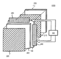
도 1은 본 발명의 실시 형태 1에 따른 액정 표시 장치(1000)의 구성을 모식적으로 나타낸 사시도이다.
도 2는 액정 표시 장치(1000)의 TFT 기판(반도체 장치(100))의 구성을 모식적으로 나타낸 평면도이다.
도 3은 TFT 기판(100)의 표시 영역 DA의 구성을 모식적으로 나타낸 평면도이다.
도 4는 실시 형태 1에 따른 TFT(10)의 구성을 모식적으로 나타낸 단면도이다.
도 5는 실시 형태 1에 따른 TFT(10)의 구성을 모식적으로 나타낸 단면도로서, TFT(10)에 의한 효과를 설명하기 위한 도면이다.
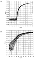
도 6의 (a) 및 도 6의 (b)는 TFT(10)에 의한 효과를 설명하기 위한 그래프로서, 도 6의 (a)는 산소 공급층을 갖는 TFT의 전압-전류 특성을 나타내고 있으며, 도 6의 (b)는 산소 공급층을 갖지 않는 TFT의 전압-전류 특성을 나타내고 있다.
도 7의 (a) 내지 도 7의 (d)는 TFT 기판(100)의 제조 공정을 모식적으로 나타낸 단면도이다.
도 8의 (e) 내지 도 8의 (g)는 TFT 기판(100)의 제조 공정을 모식적으로 나타낸 단면도이다.
도 9는 TFT 기판(100)에서의 상부 배선과 하부 배선의 접속부의 제1 구성예를 모식적으로 나타낸 단면도이다.
도 10은 TFT 기판(100)에서의 접속부의 제2 구성예를 모식적으로 나타낸 단면도이다.
도 11은 TFT 기판(100)에서의 접속부의 제3 구성예를 모식적으로 나타낸 단면도이다.
도 12는 본 발명의 실시 형태 2에 따른 TFT 기판(100)의 구성을 모식적으로 나타낸 단면도이다.
도 13은 실시 형태 2에 따른 TFT 기판(100)의 제1 변형예의 구성을 모식적으로 나타낸 단면도이다.
도 14는 실시 형태 2에 따른 TFT 기판(100)의 제2 변형예의 구성을 모식적으로 나타낸 단면도이다.
도 15는 본 발명의 실시 형태 3에 따른 TFT 기판(100)의 화소(50)의 구성을 모식적으로 나타낸 평면도이다.
도 16은 실시 형태 3에 따른 TFT 기판(100)의 구성을 모식적으로 나타낸 단면도이다.
도 17은 실시 형태 3에 따른 화소(50)의 변형예의 구성을 모식적으로 나타낸 평면도이다.
도 18은 본 발명의 실시 형태 4에 따른 TFT(10)의 구성을 모식적으로 나타낸 단면도이다.
도 19는 본 발명의 실시 형태 5에 따른 TFT(10)의 구성을 모식적으로 나타낸 단면도이다.
도 20은 본 발명의 실시 형태 6에 따른 TFT(10)의 구성을 모식적으로 나타낸 단면도이다.
도 21은 본 발명의 실시 형태 7에 따른 TFT(10)의 구성을 모식적으로 나타낸 단면도이다.
도 22는 실시 형태 7의 TFT(10)에 의한 효과를 설명하기 위한 그래프로서, 실시 형태 7의 TFT(10)의 전압-전류 특성을 나타내고 있다.
도 23은 본 발명의 실시 형태 8에 따른 TFT(10)의 구성을 모식적으로 나타낸 단면도이다.
도 24는 본 발명의 실시 형태 9에 따른 TFT(10)의 구성을 모식적으로 나타낸 단면도이다.
도 25는 본 발명의 실시 형태 10에 따른 TFT(10)의 구성을 모식적으로 나타낸 단면도이다.
도 26은 본 발명의 실시 형태 11에 따른 TFT(10)의 구성을 모식적으로 나타낸 단면도이다.
도 27은 본 발명의 실시 형태 12에 따른 TFT(10)의 구성을 모식적으로 나타낸 단면도이다.
도 28은 본 발명의 실시 형태 13에 따른 TFT(10)의 구성을 모식적으로 나타낸 단면도이다.
도 29는 본 발명의 실시 형태 14에 따른 유기 EL 표시 장치(1002)의 구성을 모식적으로 나타낸 단면도이다.
도 30의 (a)는 종래의 TFT 기판의 개략을 나타내는 모식적인 평면도이며, 도 30의 (b)는 도 30의 (a)의 TFT 기판에서의 1개의 화소를 나타낸 확대 평면도이다.
도 31은 도 30에 도시한 종래의 TFT 기판에서의 TFT 및 단자부의 단면도이다.1 is a perspective view schematically showing the configuration of a liquid
2 is a plan view schematically showing the configuration of a TFT substrate (semiconductor device 100) of the liquid
3 is a plan view schematically showing the configuration of the display area DA of the
4 is a cross-sectional view schematically showing the configuration of the
FIG. 5 is a cross-sectional view schematically showing the configuration of the
6 (a) and 6 (b) are graphs for explaining the effect by the
7A to 7D are cross-sectional views schematically showing the manufacturing process of the
8 (e) to 8 (g) are cross-sectional views schematically showing the manufacturing process of the
9 is a cross-sectional view schematically showing a first configuration example of the connection portion between the upper wiring and the lower wiring in the
10 is a cross-sectional view schematically showing a second configuration example of the connecting portion in the
11 is a cross-sectional view schematically showing a third configuration example of the connecting portion in the
12 is a cross-sectional view schematically showing the configuration of a
13 is a cross-sectional view schematically showing the configuration of a first modification of the
14 is a cross-sectional view schematically showing the configuration of a second modification of the
15 is a plan view schematically showing the configuration of a
16 is a cross-sectional view schematically showing the configuration of the
17 is a plan view schematically illustrating a configuration of a modification of the
18 is a cross-sectional view schematically showing the configuration of the
19 is a cross-sectional view schematically showing the configuration of a
20 is a cross-sectional view schematically showing the configuration of the
21 is a cross-sectional view schematically showing the configuration of the
FIG. 22 is a graph for explaining the effect of the
Fig. 23 is a sectional view schematically showing the configuration of the
24 is a cross-sectional view schematically showing the configuration of the
25 is a cross-sectional view schematically showing the configuration of the
26 is a cross-sectional view schematically showing the configuration of the
27 is a cross-sectional view schematically showing the configuration of a
28 is a cross-sectional view schematically showing the configuration of the
29 is a cross-sectional view schematically showing the configuration of an organic
FIG. 30A is a schematic plan view showing an outline of a conventional TFT substrate, and FIG. 30B is an enlarged plan view showing one pixel in the TFT substrate of FIG. 30A.
FIG. 31 is a cross-sectional view of the TFT and the terminal portion in the conventional TFT substrate shown in FIG.
이하, 도면을 참조하면서, 본 발명의 실시 형태에 따른 표시 장치, 반도체 장치를 설명한다. 단, 본 발명의 범위는 이하의 실시 형태에 한정되는 것은 아니다. 본 발명의 반도체 장치는, 산화물 반도체 TFT가 형성된 TFT 기판이며, 각종 표시 장치나 전자 기기 등의 TFT 기판을 넓게 포함하는 것으로 한다. 본 실시 형태의 설명에서는, 반도체 장치를, 산화물 반도체 TFT를 스위칭 소자로서 구비한 표시 장치의 TFT 기판으로서 설명한다.EMBODIMENT OF THE INVENTION Hereinafter, the display device and semiconductor device which concern on embodiment of this invention are demonstrated, referring drawings. However, the scope of the present invention is not limited to the following embodiment. The semiconductor device of the present invention is a TFT substrate on which an oxide semiconductor TFT is formed, and includes a TFT substrate such as various display devices and electronic devices widely. In the description of the present embodiment, the semiconductor device will be described as the TFT substrate of the display device provided with the oxide semiconductor TFT as the switching element.
(실시 형태 1)(Embodiment 1)
도 1은, 본 발명의 실시 형태에 따른 액정 표시 장치(1000)의 구성을 모식적으로 나타낸 사시도이다.1 is a perspective view schematically showing the configuration of a liquid
도 1에 도시한 바와 같이, 액정 표시 장치(1000)는 액정층을 사이에 두고 서로 대향하는 TFT 기판(100: 반도체 장치) 및 대향 기판(200)과, TFT 기판(100) 및 대향 기판(200) 각각의 외측에 배치된 편광판(210 및 220)과, 표시용 광을 TFT 기판(100)을 향해 출사하는 백라이트 유닛(230)을 구비하고 있다. TFT 기판(100)에는, 복수의 주사선(게이트 버스 라인)을 구동하는 주사선 구동 회로(240) 및 복수의 신호선(데이타 버스 라인)을 구동하는 신호선 구동 회로(250)가 배치되어 있다. 주사선 구동 회로(240) 및 신호선 구동 회로(250)는 TFT 기판(100)의 내부 또는 외부에 배치된 제어 회로(260)에 접속되어 있다. 제어 회로(260)에 의한 제어에 따라서, 주사선 구동 회로(240)로부터 TFT의 온-오프를 전환하는 주사 신호가 복수의 주사선에 공급되고, 신호선 구동 회로(250)로부터 표시 신호(도 3에 도시한 화소 전극(20)에의 인가 전압)가 복수의 신호선에 공급된다.As illustrated in FIG. 1, the liquid
대향 기판(200)은 컬러 필터 및 공통 전극을 구비하고 있다. 컬러 필터는, 3원색 표시의 경우, 각각이 화소에 대응하여 배치된 R(적색) 필터, G(녹색) 필터 및 B(청색) 필터를 포함한다. 대향 기판(200)을 4원색 이상의 표시 방식에 대응시켜도 된다. 공통 전극은, 액정층을 끼워서 복수의 화소 전극(20)을 덮도록 형성되어 있다. 공통 전극과 각 화소 전극(20) 사이에 공급되는 전위차에 따라서 양쪽 전극 사이의 액정 분자가 화소마다 배향되고, 표시가 이루어진다.The opposing
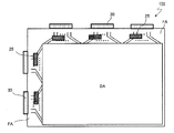
도 2는, TFT 기판(100)의 구성을 모식적으로 나타낸 평면도이며, 도 3은, TFT 기판(100)의 표시 영역 DA의 구성을 모식적으로 나타낸 평면도이다.2 is a plan view schematically showing the configuration of the
도 2에 도시한 바와 같이, TFT 기판(100)은 표시부 DA와 표시부 DA의 외측에 위치하는 주변부 FA를 갖는다. 주변부 FA에는, 도 1에 도시한 주사선 구동 회로(240) 및 신호선 구동 회로(250), 전압 공급 회로의 전기 소자 등이, 예를 들어 COG(Chip on Glass) 방식에 의해 배치되어 있다. 주변부 FA에서의 TFT, 다이오드 등의 전기 소자는, 표시부 DA의 TFT와 동일한 제조 공정에 의해 형성될 수 있다. 또한, 주변부 FA의 외측 단부 부근에는 FPC(Flexible Printed Circuits) 등의 외부 소자를 부착하기 위한 단자부(30)가 배치되어 있다. 또한, 주변부 FA에는, 신호선 등의 상부 배선과 주사선 등의 하부 배선을 전기적으로 접속하는 접속부(25)가 형성되어 있다.As shown in FIG. 2, the
도시는 생략하였지만, 표시 영역 DA와 주변 영역 FA의 경계에는 복수의 접속 배선이 배치되어 있다. 각 신호선(12)은 각각에 대응하여 형성된 접속부를 통하여 접속 배선에 전기적으로 접속되어 있다. 접속부에 의해, 상부 배선인 신호선(12)이 하부 배선인 접속 배선에 접속된다.Although not shown, a plurality of connection wirings are arranged at the boundary between the display area DA and the peripheral area FA. Each
도 3에 도시한 바와 같이, 표시부 DA에는, 복수의 화소(50)가 매트릭스 형상으로 배치되어 있으며, 복수의 주사선(14)과 복수의 신호선(12)이 서로 직교하도록 연장되어 있다. 주사선(14)의 일부는 TFT(10)의 게이트 전극을 구성한다. 복수의 주사선(14)과 복수의 신호선(12)의 교점 각각의 부근에는, 능동 소자인 박막 트랜지스터(10: TFT)가 화소(50)마다 형성되어 있다. 각 화소(50)에는, TFT(10)의 드레인 전극에 전기적으로 접속된, 예를 들어 ITO(Indium Tin Oxide)를 포함하여 이루어지는 화소 전극(20)이 배치되어 있다. 또한, 인접하는 2개의 주사선(14) 사이에는 보조 용량선(16: 'Cs 라인'이라고도 함)이 주사선(14)과 평행하게 연장되어 있다.As shown in FIG. 3, in the display portion DA, a plurality of
각 화소(10) 내에는 보조 용량(18: Cs)이 형성되어 있으며, 보조 용량선(16)의 일부가 보조 용량(18)의 보조 용량 전극(하부 전극)을 이루고 있다. 이 보조 용량 전극과, 보조 용량 대향 전극(상부 전극)과, 양쪽 전극의 사이에 배치된 층에 의해 보조 용량(18)이 구성된다. TFT(10)의 드레인 전극은 보조 용량의 보조 용량 대향 전극에 접속되어 있으며, 보조 용량 대향 전극은 층간 절연층에 형성된 콘택트 홀을 통하여 화소 전극(20)에 접속되어 있다. TFT(10)의 게이트 전극, 주사선(14), 보조 용량선(16) 및 보조 용량 전극은, 기본적으로 동일한 재료에 의해 동일한 공정으로 형성된다. TFT(10)의 소스 전극과 드레인 전극, 신호선(12), 보조 용량 대향 전극은, 기본적으로 동일한 재료에 의해 동일한 공정으로 형성된다.A storage capacitor 18 (Cs) is formed in each
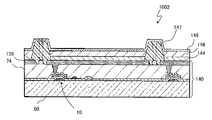
도 4는, 실시 형태 1에 따른 TFT 기판(100: '반도체 장치(100)'라고 하는 경우도 있음)에서의 TFT(10)의 구성을 모식적으로 나타낸 단면도이다.4 is a cross-sectional view schematically showing the configuration of the
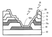
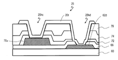
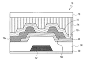
도 4에 도시한 바와 같이, TFT(10)는, 유리 기판 등의 기판(60) 위에 형성된 게이트 전극(62)과, 기판(60) 위에 게이트 전극(62)을 덮도록 형성된 게이트 절연층(66: 단순히 '절연층(66)'이라고 하는 경우도 있음)과, 게이트 절연층(66) 위에 형성된 산화물 반도체층(68)과, 게이트 절연층(66) 및 산화물 반도체층(68) 위에 형성된 소스 전극(70s) 및 드레인 전극(70d)과, 소스 전극(70s) 및 드레인 전극(70d) 위에 형성된 보호층(72)과, 보호층(72) 위에 형성된 산소 공급층(74)과, 산소 공급층(74) 위에 형성된 확산 방지층(78)을 구비하고 있다.As shown in FIG. 4, the
나중에 도 12 내지 14에 도시한 바와 같이, 확산 방지층(78) 위에는 투명 도전 재료에 의한 화소 전극(20)이 형성되어 있다. 화소 전극(20) 아래의 확산 방지층(78), 층간 절연층(74) 및 보호층(72)에는 콘택트 홀이 형성되어 있으며, 화소 전극(20)은 그 콘택트 홀의 바닥에서 TFT(10)의 드레인 전극(70d)과 접하고 있다.12 to 14, a
게이트 전극(62)은 예를 들어 티타늄(Ti)을 포함하여 이루어지는 하층 게이트 전극 위에, 예를 들어 구리(Cu)를 포함하여 이루어지는 상층 게이트 전극이 형성된 2층 구조를 가질 수 있다. 게이트 전극을, Ti/Al(알루미늄)/Ti 등의 3층 구성으로 해도 된다. 게이트 절연층(66)은 질화실리콘에 의해 형성되어 있다. 게이트 절연층(66)을 산화실리콘으로 형성해도 되며, 질화실리콘층과 산화실리콘층의 2층 구성으로 형성할 수도 있다.The
산화물 반도체층(68)은 In-Ga-Zn-O계 반도체(IGZO)를 포함하여 이루어지는 층이다. 산화물 반도체층(68) 위에 형성된 소스 전극(70s) 및 드레인 전극(70d)은 Ti/Al/Ti의 3층 구성을 포함하여 이루어지는 도전층이다. 소스 전극(70s) 및 드레인 전극(70d)을 Al/Ti, Cu/Ti, Cu/Mo(몰리브덴) 등의 2층 구성으로 해도 된다. 보호층(72)은 산화실리콘(SiO2) 또는 질화실리콘(SiNx)에 의해 형성되어 있다. 보호층(72)을 형성하지 않는 구성도 있을 수 있다. 확산 방지층(78)은 산화실리콘(SiO2), 질화실리콘(SiNx) 또는 산질화실리콘(SiNO)에 의해 형성되어 있다.The
산소 공급층(74)은 물(H2O), OR기 또는 OH기를 함유하는 재료를 포함하여 이루어지는 층이다. 본 실시 형태에서는, 산소 공급층(74)은 예를 들어 아크릴 수지를 스핀 코트법에 의해 도포하여 형성되어 있다. SOG 재료에는, 실리콘(silicone) 수지, 실란올(예를 들어 Si(OH)4), 알콕시실란, 실록산 수지 등을 함유하는 스핀온 글라스(SOG) 재료를 이용할 수 있다. 산소 공급층(74)을 실라놀기 또는 Si-OH기를 함유하는 다른 수지 재료로 형성해도 된다. 또한, 산소 공급층(74)은 에스테르 중합 수지 또는 CO-OR기를 함유하는 수지 재료에 의해 형성할 수도 있다.The
도 5에 도시한 바와 같이, 산소 공급층(74)이 H2O, OR기 또는 OH기를 함유하기 때문에, 어닐 등의 열처리 공정에서, 산소 공급층(74)으로부터 보호층(72)을 통하여 산화물 반도체층(68)의 채널부에 H2O, OH기 또는 OR기가 확산되어, 산화물 반도체층(68) 중의 산소 결손 등에 기인한 결함이 보완된다. 이에 의해, TFT의 특성이 향상되어, TFT마다의 변동이 적은, 고품질의 반도체 장치를 제공할 수 있다. 또한, 산화물 반도체층(74)의 상부에 확산 방지층(78)이 배치되어 있기 때문에, 산소 공급층(74)으로부터 위쪽으로 이동한 H2O, OR기 또는 OH기가, 확산 방지층(78)의 저면에서 반사되어 산화물 반도체층(68)을 향해 이동한다. 따라서, 확산 방지층(78)을 형성한 후에 열처리를 행하는 경우, 산화물 반도체층(68)에 보다 많은 H2O, OR기 또는 OH기의 공급이 이루어져서, 보다 많은 결함이 수복된다.As shown in FIG. 5, since the
도 6의 (a)는 복수의 TFT(10)의 전압-전류 특성을 나타낸 그래프이며, (b)는 산소 공급층 및 확산 방지층을 갖지 않는 복수의 TFT의 전압-전류 특성을 나타낸 그래프이다. 양 그래프에서, 횡축은 게이트 전압값을 나타내고, 종축은 소스-드레인 전류값을 나타낸다. 도 6의 (a)로부터 알 수 있는 바와 같이, 실시 형태 1의 TFT(10)에서는, 게이트 전압 0V 부근에서의 전류의 상승이 급격하면서, 복수의 TFT(10)의 특성(S값) 사이에 변동이 적다. 이것은, 어느 TFT(10)에서도, TFT(10)가 ON일 때부터 인가 전압에 따른 적절한 전류값이 얻어지는 것을 나타내고 있다. 한편, 도 6의 (b)에 도시된 바와 같이, 산소 공급층 및 확산 방지층을 갖지 않는 TFT에서는, ON 전류의 상승이 둔하여, 상승 위치에 큰 변동이 보인다. 또한, OFF 전류값에도 변동이 발생하였다. 이들 비교로부터, 실시 형태 1의 TFT(10)에 의하면, 보다 TFT 특성이 안정된 고성능의 반도체 장치가 얻어지는 것을 알 수 있다.6A is a graph showing the voltage-current characteristics of the plurality of
이어서, 도 7 및 도 8을 참조하면서 TFT 기판(100)의 제조 방법을 설명한다.Next, a manufacturing method of the
도 7의 (a) 내지 (d) 및 도 8의 (e) 내지 (g)는, TFT 기판(100)의 제조 공정을 나타낸 모식적인 단면도이다.7A to 7D and FIG. 8E to FIG. 8G are schematic cross-sectional views showing the manufacturing process of the
공정 (A):Process (A):
우선, 기판(60) 위에 스퍼터링법 등에 의해, Ti층 및 Cu층을 이 순서로 적층한다. Ti층의 두께는 30 내지 150㎚이며, Cu층의 두께는 200 내지 500㎚이다. 이어서, 적층한 2층을 공지된 포토리소그래피법 및 웨트 에칭법을 이용하여 패터닝하여(제1 마스크 공정), 도 7의 (a)에 도시한 게이트 전극(62)을 얻는다. 이때, 여기에서는 도시를 생략한 주사선(14), 보조 용량선(16), 보조 용량 전극, 하부 배선 등도 동시에 형성된다. 그 후, 남은 레지스트의 박리 및 기판의 세정이 행해진다.First, Ti layer and Cu layer are laminated | stacked on this board |
공정 (B):Process (B):
이어서, 기판(60) 위에 게이트 전극(62)을 덮도록 게이트 절연층(66)을 적층한다. 게이트 절연층(66)은 플라즈마 CVD법에 의해 두께 100 내지 700㎚로 적층된 질화실리콘층이다. 질화실리콘 대신에 산화실리콘(SiO2)을 적층해도 되고, 질화실리콘과 산화실리콘을 모두 적층해도 된다.Subsequently, the
이어서, 도 7의 (b)에 도시한 바와 같이, 게이트 절연층(66) 위에 산화물 반도체 재료(68m)를 적층한다. 산화물 반도체 재료(68m)는 예를 들어 In-Ga-Zn-O(IGZO)이며, 스퍼터링법에 의해 두께 10 내지 100㎚ 적층된다. 산화물 반도체 재료(68m)를 도포법 또는 잉크젯법에 의해 적층해도 된다. 산화물 반도체 재료에는, IGZO 대신에 다른 종류의 산화물 반도체막을 이용해도 된다.Subsequently, as shown in FIG. 7B, an
공정 (C):Process (C):
그 후, 적층한 산화물 반도체 재료(68m)를 포토리소그래피법, 예를 들어 옥살산을 이용한 웨트 에칭법으로 패터닝하여(제2 마스크 공정), 도 7의 (c)에 도시한 바와 같이, TFT(10)의 채널층을 포함하는 산화물 반도체층(68)을 얻는다. 그 후, 남은 레지스트의 박리 및 기판의 세정이 행해진다.Thereafter, the stacked
공정 (D):Process (D):
이어서, 스퍼터링법에 의해, 게이트 절연층(66) 위에 산화물 반도체층(68)을 덮도록, Ti, Al 및 Ti을 이 순서로 적층한다. 이어서, 포토리소그래피법 및 웨트 에칭법에 의해, 이들 3층을 패터닝하여, 도 7의 (d)에 도시한 바와 같이, 소스 전극(70s) 및 드레인 전극(70d)을 얻는다(제3 마스크 공정). 그 후, 남은 레지스트의 제거 및 기판 세정이 이루어진다. 웨트 에칭 대신에 드라이 에칭을 이용하는 것도 가능하다. Ti, Al 및 Ti을 적층하는 대신에, Al/Ti, Al/Mo, Cu/Ti 또는 Cu/Mo을 적층해도 된다. 또한 이들 금속을 단층으로 이용할 수도 있다. 이 공정에서는, 여기에서는 도시를 생략한 신호선(12), 보조 용량 대향 전극, 상부 배선 등도 동시에 형성된다.Next, Ti, Al, and Ti are laminated in this order so as to cover the
공정 (E):Process (E):
이어서, 도 8의 (e)에 도시한 바와 같이, CVD법에 의해 산화실리콘을 기판 전체에 적층하여, 보호층(72)을 형성한다. 산화실리콘 대신에 질화실리콘을 적층해도 되며 또한, 산화실리콘 및 질화실리콘을 모두 적층해도 된다. 보호층(72)의 두께는, 25nm 내지 350㎚이다. 보호층(72)의 두께가 이보다도 얇은 경우, 보호층으로서의 기능이 떨어져서, TFT의 신뢰성이 저하된다. 이보다도 두꺼운 경우에는, 막 응력 등에 의한 막 박리가 염려된다. 또한 그 경우, 보호층(72)의 성막 및 에칭에 시간이 걸려서, 생산성이 나빠진다.Subsequently, as shown in FIG. 8E, the silicon oxide is laminated on the entire substrate by the CVD method to form the
공정 (F):Process (F):
이어서, 도 8의 (f)에 도시한 바와 같이, 보호층(72) 위에 아크릴 수지의 산소 공급 재료(74m)를 도포한다. 실리콘 수지 등의 SOG 재료를 스핀 코트로 도포해도 된다. 산소 공급 재료(74m)로서, 실란올(Si(OH)4), 알콕시실란, 실록산 수지 등을 함유하는 재료를 이용할 수 있다. 산소 공급층(74)을 실라놀기 또는 Si-OH기를 함유하는 다른 수지 재료로 형성해도 된다. 또한, 산소 공급층(74)은 에스테르 중합 수지 또는 CO-OR기를 함유하는 수지 재료에 의해 형성할 수도 있다. 산소 공급층(74)의 두께는, 500nm 내지 3500㎚이다. 산소 공급층(74)의 두께가 이보다도 얇은 경우, 발명의 효과를 얻지 못할 우려가 있으며, 또한, 이보다도 두꺼운 경우에는, 막 박리 및 생산성의 저하가 염려된다.Subsequently, as illustrated in FIG. 8F, an oxygen supply material 74m of an acrylic resin is applied onto the
공정 (G):Process (G):
이어서, 산소 공급층(74) 위에 CVD법에 의해 산화실리콘을 기판 전체에 적층하여, 도 8의 (g)에 도시한 바와 같이, 확산 방지층(78)을 형성한다. 산화실리콘 대신에 질화실리콘을 적층해도 되며, 또한, 산화실리콘 및 질화실리콘을 모두 적층해도 된다.Subsequently, silicon oxide is laminated on the whole substrate by the CVD method on the
확산 방지층(78)의 두께는, 50nm 내지 500㎚이다. 그 후, 대기 분위기 중에서, 200℃ 내지 400℃의 온도로 어닐 처리를 행하여, TFT(10)가 완성된다. 확산 방지층(78)을 질화실리콘막, 또는 산화실리콘과 질화실리콘막의 적층막으로 하고, 보호층(72)을 실리콘 산화막으로 함으로써, 확산 방지층(78)에 의한 높은 확산 방지 효과와 보호층(72)에 의한 보호막 기능을 양립시키는 것이 가능해진다. 또한, 보호층(72)에는 보호막으로서의 기능과 H2O, OR기 또는 OH기를 적당히 투과하는 성질이 필요하다. 질화실리콘막은 산화실리콘막에 비해, H2O, OR기 또는 OH기를 투과하기 어려운 성질을 갖는다.The thickness of the
어닐 처리 시에, 산소 공급층(74)으로부터 보호층(72)을 통하여 산화물 반도체층(68)의 채널부에, H2O, OH기 또는 OR기가 확산되어, 산화물 반도체층(68) 중의 산소 결손 등에 기인한 결함이 보완된다. 또한, 산소 공급층(74)으로부터 위쪽으로 이동한 H2O, OR기 또는 OH기가, 확산 방지층(78)의 저면에서 반사되어 산화물 반도체층(68)을 향해 이동한다. 따라서, 산화물 반도체층(68)에 H2O, OR기 또는 OH기의 공급이 이루어져서, 보다 결함이 수복된다.At the time of annealing, H 2 O, an OH group or an OR group diffuses from the
그 후, 확산 방지층(78) 위에, 예를 들어 스퍼터링법에 의해 투명 도전 재료를 퇴적한다. 이때 투명 도전 재료는, 드레인 전극(70d) 위의 보호층(72), 산소 공급층(74) 및 확산 방지층(78)에 형성된 콘택트 홀 내에도 적층되고, 콘택트 홀의 저부에서 드레인 전극(70d)과 접한다. 투명 도전 재료로서는, ITO를 이용한다. 투명 도전 재료에 IZO, ZnO 등을 이용해도 된다. 계속해서, 공지된 포토리소그래피법에 의해, 투명 전극층의 패터닝을 행하여 화소 전극(20)이 형성된다.Thereafter, a transparent conductive material is deposited on the
이상의 공정에 의해, TFT(10)를 갖는 TFT 기판(100)이 완성된다.By the above process, the
이어서, 도 9 내지 도 11을 참조하여, TFT 기판(100)에서의 접속부(25)의 제1 내지 제3 구성예를 설명한다. 도 9 내지 도 11은, 각각, 접속부(25)의 제1 내지 제3 구성예의 단면을 모식적으로 나타낸다.Next, with reference to FIGS. 9-11, the 1st-3rd structural example of the
제1 구성예:First configuration example:
제1 구성예에 따른 접속부(25)는 도 9에 도시한 바와 같이, 기판(60) 위에 형성된 하부 배선(62d)과, 하부 배선(62d) 위에 형성된 게이트 절연층(66)과, 게이트 절연층(66) 위에 형성된 산화물 반도체층(68)과, 산화물 반도체층(68) 위에 형성된 상부 배선(70u)을 구비하고 있다. 산화물 반도체층(68)이 배치되지 않은 형태도 있을 수 있다. 하부 배선(62d)은 게이트 전극(62)과 동시에 동일한 재료로 형성된 금속층이다. 상부 배선(70u)은 소스 전극(70s) 및 드레인 전극(70d)과 동시에 동일한 재료로 형성된 금속층이다.As shown in FIG. 9, the
접속부(25)에서, 산화물 반도체층(68) 및 게이트 절연층(66)의 각각에는, 서로 겹치는 위치에 개구가 형성되어 있으며, 이들 2층을 관통하도록 콘택트 홀(25ha)이 형성되어 있다. 게이트 절연층(66)의 개구는 산화물 반도체층(68)의 개구보다도 크고, 콘택트 홀(25ha)에서, 게이트 절연층(66) 및 산화물 반도체층(68)의 측면은 계단 형상으로 형성되어 있다. 상부 배선(70u)과 하부 배선(62d)은, 콘택트 홀(25ha)을 통하여 접속되어 있다. 즉, 콘택트 홀(25ha) 내에 형성된 상부 배선(70u)이 콘택트 홀(25ha)의 저부에서 하부 배선(62d)과 접속되어 있다. 또한, 접속부(25)에 산화물 반도체층(68)이 배치되지 않은 형태에서는, 콘택트 홀(25ha)은, 게이트 절연층(66)만을 관통하도록 형성된다.In the
상부 배선(70u)의 금속층을 적층하는 경우, 콘택트 홀(25ha)의 측면이 급경사면이면, 측면에서 금속층의 절단이 생기기 쉬워, 접속부에서의 단선이 발생할 우려가 있다. 본 구성예에서는, 상부 배선(70u)이 급경사의 측면이 아니라, 게이트 절연층(66) 및 산화물 반도체층(68)의 계단 형상의 측면 위에 형성되기 때문에, 상부 배선(70u)의 절단이 생기기 어렵다. 따라서, 신뢰성이 높은 접속부(25)를 형성할 수 있다.When the metal layer of the
제2 구성예:Second configuration example:
제2 구성예에 따른 접속부(25)는 도 10에 도시한 바와 같이, 기판(60) 위에 형성된 하부 배선(62d)과, 하부 배선(62d) 위에 형성된 게이트 절연층(66)과, 게이트 절연층(66) 위에 형성된 상부 배선(70u)과, 상부 배선(70u) 위에 형성된 보호층(72)과, 보호층(72) 위에 형성된 산소 공급층(74)과, 산소 공급층(74) 위에 형성된 확산 방지층(78)과, 확산 방지층(78) 위에 형성된 도전층(20t)을 구비하고 있다. 하부 배선(62d)은 게이트 전극(62)과 동시에 동일한 재료로 형성된 금속층이며, 상부 배선(70u)은 소스 전극(70s) 및 드레인 전극(70d)과 동시에 동일한 재료로 형성된 금속층이다. 도전층(20t)은 화소 전극(20)과 동시에 동일한 재료로 형성되어 있다.As shown in FIG. 10, the
접속부(25)에서, 게이트 절연층(66), 상부 배선(70u), 보호층(72), 산소 공급층(74) 및 확산 방지층(78)의 각각에는, 서로 겹치는 위치에 개구가 형성되어 있다. 개구는, 하층으로부터 상층을 향해 커지도록 형성되어 있으며, 이들 층을 관통하도록 콘택트 홀(25hb)이 형성되어 있다. 콘택트 홀(25hb)에서, 각 층의 단부는, 보다 상층으로 될수록 보다 외측에 위치하도록, 계단 형상으로 형성되어 있다.In the
상부 배선(70u)과 하부 배선(62d)은, 콘택트 홀(25hb) 내의 도전층(20t)을 통하여 접속되어 있다. 즉, 콘택트 홀(25hb) 내에는, 게이트 절연층(66), 상부 배선(70u), 보호층(72), 산소 공급층(74) 및 확산 방지층(78)의 측면을 덮도록 도전층(20t)이 형성되어 있으며, 그 측면에서 도전층(20t)과 상부 배선(70u)이 접속되고, 콘택트 홀(25hb)의 저부에서 도전층(20t)과 하부 배선(62d)이 접속되어 있다.The
콘택트 홀(25hb) 내에 도전층(20t)을 형성하는 경우, ITO, IZO 등의 금속이 스퍼터링법에 의해 적층되지만, 콘택트 홀(25hb)의 측면이 급경사면이면, 금속층의 절단이나 금속층과 상부 배선(70u)의 접촉 불량이 발생하기 쉽다. 또한, 각 층의 단부가 동일한 위치가 되도록 형성하려고 하면, 포토리소그래피에서의 마스크의 위치 어긋남, 에칭 시프트의 변동, 오버행 등에 의해, 하층의 단부가 상층의 단부보다도 외측에 형성되는 경우가 생길 수 있다. 이것은 도전층(20t)에 단선을 야기하는 원인이 된다.When the
본 구성예에서는, 각 층의 측면이, 보다 상층으로 될수록 보다 외측에 위치하도록 형성되기 때문에, 콘택트 홀(25hb)의 측면이 계단 형상으로 형성되고, 도전층(20t)의 단선 및 도전층(20t)과 상부 배선(70u)의 접촉 불량이 방지된다. 또한, 다층 구성 부위에서의 접속을 하나의 콘택트 홀을 통하여 행하기 때문에, 접속부의 면적을 작게 억제할 수 있다. 이에 의해, TFT 기판의 고밀도화, 소형화가 가능해진다. 또한, 콘택트 홀(25hb)을, 각 층의 에칭을 하프톤 노광, 레지스트 애싱 등을 이용하여, 일괄적으로 행하여 형성할 수도 있다. 이 경우, 제조 효율이 향상되어, TFT 기판을 저비용으로 제조하는 것이 가능해진다.In this configuration example, the side surface of each layer is formed so as to be located outside as the upper layer becomes higher. Therefore, the side surface of the contact hole 25hb is formed in a step shape, and the disconnection and the
제3 구성예:Third configuration example:
제3 구성예에 따른 접속부(25)는 도 11에 도시한 바와 같이, 기판(60) 위에 형성된 하부 배선(62d)과, 하부 배선(62d) 위에 형성된 게이트 절연층(66)과, 게이트 절연층(66) 위에 형성된 상부 배선(70u)과, 상부 배선(70u) 위에 형성된 보호층(72)과, 보호층(72) 위에 형성된 산소 공급층(74)과, 산소 공급층(74) 위에 형성된 확산 방지층(78)과, 확산 방지층(78) 위에 형성된 도전층(20t)을 구비하고 있다. 하부 배선(62d)은 게이트 전극(62)과 동시에 동일한 재료로 형성된 금속층이며, 상부 배선(70u)은 소스 전극(70s) 및 드레인 전극(70d)과 동시에 동일한 재료로 형성된 금속층이다. 도전층(20t)은 화소 전극(20)과 동시에 동일한 재료로 형성되어 있다.As shown in FIG. 11, the
접속부(25)에는, 확산 방지층(78), 산소 공급층(74) 및 보호층(72)을 관통하는 제1 콘택트 홀(25hc)과, 확산 방지층(78), 산소 공급층(74), 보호층(72) 및 게이트 절연층(66)을 관통하는 제2 콘택트 홀(25hd)이 형성되어 있다. 상부 배선(70u)과 도전층(20t)은, 제1 콘택트 홀(25hc) 내에서 접속되어 있다. 즉, 콘택트 홀(25hc) 내에는, 확산 방지층(78), 산소 공급층(74) 및 보호층(72)의 측면을 덮도록 도전층(20t)이 형성되어 있으며, 콘택트 홀(25hc)의 저부에서 도전층(20t)과 상부 배선(70u)이 접속되어 있다. 도전층(20t)과 하부 배선(62d)은, 제2 콘택트 홀(25hd) 내에서 접속되어 있다. 즉, 콘택트 홀(25hd) 내에는, 확산 방지층(78), 산소 공급층(74), 보호층(72) 및 게이트 절연층(66)의 측면을 덮도록 도전층(20t)이 형성되어 있으며, 콘택트 홀(25hd)의 저부에서 도전층(20t)과 하부 배선(62d)이 접속되어 있다.In the
이와 같이 하여, 상부 배선(70u)과 하부 배선(62d)이 도전층(20t)을 통하여 전기적으로 접속되어 있다. 제1 및 제2 구성예와 마찬가지로, 콘택트 홀(25hc 및 25hd)의 측면을 계단 형상으로 형성해도 되며, 그것에 의해, 도전층(20t)의 단선을 방지할 수 있다.In this way, the
이어서, 본 발명에 따른 다른 실시 형태(실시 형태 2 내지 14)를 설명한다. 이하의 설명에서는, 실시 형태 1과 동일한 구성 요소에는 동일한 참조 번호를 붙이고, 그 상세한 설명을 생략한다. 마찬가지의 구성을 갖는 구성 요소로부터는 마찬가지의 효과를 얻을 수 있다. 이하의 실시 형태에서 설명하는 TFT 및 TFT 기판은, 기본적으로 실시 형태 1의 TFT(10) 및 TFT 기판(100)과 교환 가능하다.Next, another embodiment (embodiments 2 to 14) according to the present invention will be described. In the following description, the same components as those in the first embodiment are denoted by the same reference numerals, and detailed description thereof will be omitted. The same effect can be acquired from the component which has a similar structure. TFT and TFT board | substrate demonstrated in the following embodiment are basically interchangeable with
(실시 형태 2)(Embodiment 2)
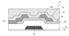
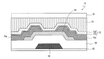
도 12는, 실시 형태 2에 따른 TFT 기판(100)의 구성을 모식적으로 나타낸 단면도이다. 본 실시 형태에 따른 TFT 기판(100)의 기본적 구성은, 이하에 설명하는 이외에는 실시 형태 1의 TFT 기판(100)과 동일하다. 본 실시 형태에 따른 TFT 기판(100)은 도 1 및 도 2에 도시한 액정 표시 장치(1000)의 TFT 기판(100)으로서 이용될 수 있다.12 is a cross-sectional view schematically showing the configuration of the
도 12에 도시한 바와 같이, TFT 기판(100)은 접속부(25)와, TFT(10)와, 보조 용량(18: Cs)을 구비하고 있다. 실시 형태 2에서의 접속부(25)의 구성은, 기본적으로 실시 형태 1의 제2 구성예의 접속부(25)와 동일하다. 단, 제2 구성예에서의 게이트 절연층(66)과 상부 배선(70u) 사이에, 산화물 반도체층(68)이 배치되어 있으며, 게이트 절연층(66), 산화물 반도체층(68), 상부 배선(70u), 보호층(72), 산소 공급층(74) 및 확산 방지층(78)을 관통하도록 콘택트 홀(25hb)이 형성되어 있다.As shown in FIG. 12, the
본 실시 형태의 접속부(25)에 있어서도, 콘택트 홀(25hb) 측면에서, 복수의 층이 보다 상층으로 될수록 보다 외측에 위치하도록 형성되기 때문에, 콘택트 홀(25hb)의 측면이 계단 형상으로 형성되고, 도전층(20t)의 단선 및 도전층(20t)과 상부 배선(70u)의 접촉 불량이 방지된다. 또한, 배선 접속을 하나의 콘택트 홀을 통하여 행하기 때문에, 접속부의 면적을 작게 억제할 수 있다. 접속부(25)로서, 실시 형태 1의 제1 또는 제3 구성예의 접속부(25)를 형성해도 된다.Also in the
보조 용량(18)이 형성된 영역('Cs 영역'이라 함)에는, 기판(60) 위에 보조 용량 전극(62c), 게이트 절연층(66), 보호층(72), 산소 공급층(74), 확산 방지층(78) 및 보조 용량 대향 전극(20c)이 이 순서로 적층되어 있다. 보조 용량 전극(62c)은 TFT(10)의 게이트 전극(62)과 동일한 공정에서 동일한 재료에 의해 형성되어 있다. 보조 용량 대향 전극(20c)은 화소 전극(20)과 동일한 공정에서 동일한 재료에 의해 형성되어 있다.In the region where the
보조 용량 전극(62c) 위에는, 게이트 절연층(66), 보호층(72) 및 산소 공급층(74)을 관통하는 개구가 형성되어 있으며, 그 개구 내에 확산 방지층(78) 및 보조 용량 대향 전극(20c)이 적층되어 있다. 개구 내에서, 확산 방지층(78)은 보조 용량 전극(62c)에 접하고 있으며, 보조 용량 대향 전극(20c)은 확산 방지층(78)에 접하고 있다. 보조 용량 전극(62c)과, 거기에 대향하는 보조 용량 대향 전극(20c)과, 양쪽 전극의 사이에 끼워진 확산 방지층(78)에 의해, 보조 용량(18)이 구성된다. 이 구성에 의해, 양쪽 전극의 간격을 좁힐 수 있으므로, 산소 공급층(74)을 포함하는 다층 구성의 TFT 기판(100)에서도, 좁은 영역에 큰 용량을 갖는 보조 용량(18)을 형성할 수 있다.On the
이어서, 도 13을 참조하면서, 실시 형태 2에 따른 TFT 기판(100)의 제1 변형예의 구성을 설명한다. 제1 변형예에 따른 TFT 기판(100)의 기본적 구성은, 이하에 설명하는 이외에는 실시 형태 2의 TFT 기판(100)과 동일하다. 이하, 서로 다른 부분을 중심으로 설명한다.Next, with reference to FIG. 13, the structure of the 1st modified example of the
도 13에 도시한 바와 같이, TFT 기판(100)은 접속부(25)와, TFT(10)와, 보조 용량(18: Cs)을 구비하고 있다. 보조 용량(18)이 형성된 Cs 영역에는, 기판(60) 위에 보조 용량 전극(62c), 게이트 절연층(66), 보호층(72), 산소 공급층(74), 투명 전극 재료를 포함하여 이루어지는 도전층(22: 제1 도전층), 확산 방지층(78) 및 보조 용량 대향 전극(20c: 제2 도전층)이 이 순서로 적층되어 있다.As shown in FIG. 13, the
보조 용량 전극(62c) 위에는, 게이트 절연층(66), 보호층(72) 및 산소 공급층(74)을 관통하는 개구가 형성되어 있으며, 그 개구 내에 도전층(22), 확산 방지층(78) 및 보조 용량 대향 전극(20c)이 적층되어 있다. 개구 내에서, 도전층(22)은 보조 용량 전극(62c)과 접하고 있으며, 확산 방지층(78)은 도전층(22)과 보조 용량 대향 전극(20c)에 끼워져 있다.An opening penetrating through the
보조 용량 전극(62c) 및 도전층(22)과, 거기에 대향하는 보조 용량 대향 전극(20c)과, 확산 방지층(78)에 의해, 보조 용량(18)이 구성된다. 이 구성에 의해, 양쪽 전극의 간격을 좁힐 수 있으므로, 산소 공급층(74)을 포함하는 다층 구성의 TFT 기판(100)에서도, 좁은 영역에 큰 용량을 갖는 보조 용량(18)을 형성할 수 있다.The
이어서, 도 14를 참조하면서, 실시 형태 2에 따른 TFT 기판(100)의 제2 변형예의 구성을 설명한다. 제2 변형예에 따른 TFT 기판(100)의 기본적 구성은, 이하에 설명하는 이외에는 실시 형태 2의 TFT 기판(100)과 동일하다. 이하, 서로 다른 부분을 중심으로 설명한다.Next, with reference to FIG. 14, the structure of the 2nd modification of the
도 14에 도시한 바와 같이, TFT 기판(100)은 접속부(25)와, TFT(10)와, 보조 용량(18: Cs)을 구비하고 있다. 보조 용량(18)이 형성된 Cs 영역에는, 기판(60) 위에 보조 용량 전극(62c), 게이트 절연층(66), 산화물 반도체층(68), 보호층(72), 산소 공급층(74), 확산 방지층(78) 및 보조 용량 대향 전극(20c)이 이 순서로 적층되어 있다.As shown in FIG. 14, the
보조 용량 전극(62c)의 상면은 게이트 절연층(66)에 덮이지 않고, 산화물 반도체층(68)에 접하고 있다. 산화물 반도체층(68) 위에는, 보호층(72) 및 산소 공급층(74)을 관통하는 개구가 형성되어 있으며, 그 개구 내에 확산 방지층(78) 및 보조 용량 대향 전극(20c)이 적층되어 있다. 개구 내에서, 산화물 반도체층(68)은 확산 방지층(78)과 접하고 있으며, 확산 방지층(78)은 보조 용량 대향 전극(20c)에 접하고 있다.The upper surface of the
보조 용량 전극(62c) 및 산화물 반도체층(68)과, 거기에 대향하는 보조 용량 대향 전극(20c)과, 확산 방지층(78)에 의해, 보조 용량(18)이 구성된다. 산화물 반도체층(68)은 열처리가 이루어짐으로써 도체화하고 있으며, 보조 용량 전극으로서의 기능을 완수한다. 따라서, 양쪽 전극의 간격을 좁힐 수 있어, 산소 공급층(74)을 포함하는 다층 구성의 TFT 기판(100)에서도, 좁은 영역에 큰 용량을 갖는 보조 용량(18)을 형성할 수 있다. 또한, Cs부에서의 산화물 반도체층(68)의 패터닝 및 열처리는, 각각 TFT(10)의 산화물 반도체층(68)의 패터닝 및 열처리와 동시에 행해진다. 따라서, 공정수를 증가시키지 않고 효율적으로 고성능의 보조 용량(18)을 형성할 수 있다.The
(실시 형태 3)(Embodiment 3)
이어서, 본 발명의 실시 형태 3에 따른 표시 장치를 설명한다. 실시 형태 3의 표시 장치는, 프린지 필드(FFS)형 액정 표시 장치이다. 실시 형태 1과 동일한 구성 요소에는 동일한 참조 번호를 붙이고, 서로 다른 부분을 중심으로 설명을 행한다.Next, the display device concerning Embodiment 3 of this invention is demonstrated. The display device of Embodiment 3 is a fringe field (FFS) type liquid crystal display device. The same components as those in the first embodiment are denoted by the same reference numerals, and the description will be mainly focused on different parts.
도 15는, 실시 형태 3에 따른 TFT 기판(100)의 화소(50)의 구성을 모식적으로 나타낸 평면도이며, 도 16은, 실시 형태 3에 따른 TFT 기판(100)의 A-A' 단면(TFT(10)의 단면) 및 B-B' 단면의 구성을 모식적으로 나타낸 단면도이다.FIG. 15 is a plan view schematically showing the configuration of a
도 15 및 도 16에 도시한 바와 같이, TFT 기판(100)은 화소(50)마다 TFT(10), TFT(10)의 드레인 전극(70d)에 접속된 상층 전극(94: 화소 전극) 및 하층 전극(92)을 구비하고 있다. TFT(10)의 구성은, 실시 형태 1 및 2에서 설명한 TFT(10)와 동일하다. TFT 기판(100)에는, 주사선(14)과 평행하게 연장하는 공통선(90)이 배치되어 있다. 주사선(14), 공통선(90) 및 인접하는 2개의 신호선(12)에 의해 둘러싸인 영역이 1개의 화소(50)에 대응하고 있다.As shown in FIG. 15 and FIG. 16, the
공통선(90)으로부터는, 화소(50)의 주변부에서 신호선(12)과 평행하게 연장되는 지선(90b)이 분기하고 있다. 지선(90b) 위의 게이트 절연층(66), 보호층(72) 및 산소 공급층(74)에는 콘택트 홀이 형성되어 있으며, 콘택트 홀 측면 및 저면에는 하층 전극(92)의 일부가 형성되어 있다. 즉, 하부 전극(92)과 지선(90b)(및 공통선(90))은, 콘택트 홀을 통하여 접속되어 있다. 공통선(90) 및 지선(90b)은 TFT(10)의 게이트 전극(62)과 동일한 공정에서 동일한 재료로 형성된다.From the
상층 전극(94)은 빗살 모양의 형태를 갖는다. 하층 전극(92)은 산소 공급층(74)과 확산 방지층(78) 사이에, 화소(50)의 거의 전체에 걸쳐 형성되어 있으며, 상층 전극(92)은 확산 방지층(78) 위에 형성되어 있다. 상층 전극(92)의 빗살 부분(서로 평행하게 연장되는 복수의 선상 부분)과 하층 전극(92) 사이에 형성되는 전계에 따라서, 상층 전극(94) 위의 액정이 배향하여, 표시가 이루어진다.The
도 17은, 실시 형태 3의 TFT 기판(100)에서의 화소(50)의 구성의 변형예를 모식적으로 나타낸 평면도이다. 도 17에 도시한 바와 같이, 변형예에서는 공통선(90)은 화소(10)의 중앙 부근을 주사선(14)과 평행하게 연장되어 있다. 지선(90b)은 형성되지 않고, 공통선(90)과 하부 전극(92)은, 공통선(90) 위에 형성된 콘택트 홀을 통하여 접속되어 있다.17 is a plan view schematically illustrating a modification of the configuration of the
(실시 형태 4)(Fourth Embodiment)
이어서, 도 18을 참조하여, 본 발명의 실시 형태 4에 따른 TFT(10)의 구성을 설명한다. 도 18은, 실시 형태 4에 따른 TFT(10)의 단면을 모식적으로 나타내고 있다.Next, with reference to FIG. 18, the structure of the
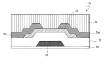
실시 형태 4의 TFT(10)는, 기판(60) 위에 형성된 게이트 전극(62)과, 게이트 전극(62) 위에 형성된 게이트 절연층(66)과, 게이트 절연층(66) 위에 형성된 산화물 반도체층(68)과, 산화물 반도체층(68) 위에 배치된 소스 전극(70s) 및 드레인 전극(70d)과, 산화물 반도체층(68), 소스 전극(70s) 및 드레인 전극(70d) 위에 산화물 반도체층(68)의 채널 부분에 접하도록 형성된 산소 공급층(74)을 구비하고 있다. 이 TFT(10)는, 실시 형태 1의 TFT(10)로부터 보호층(72)과 확산 방지층(78)을 제외한 구성을 가지며, 그 이외의 구성은 실시 형태 1과 동일하다.The
실시 형태 4의 구성에 의하면, 산화물 반도체층(68)의 채널부에 산소 공급층(74)이 직접 접하고 있기 때문에, 채널부의 결함을 효율적으로 보완할 수 있다. 단, 확산 방지층(78)에 따른 효과를 얻을 수는 없다.According to the structure of Embodiment 4, since the
(실시 형태 5)(Embodiment 5)
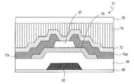
이어서, 도 19를 참조하여, 본 발명의 실시 형태 5에 따른 TFT(10)의 구성을 설명한다. 도 19는, 실시 형태 5에 따른 TFT(10)의 단면을 모식적으로 나타내고 있다.Next, with reference to FIG. 19, the structure of the
실시 형태 5의 TFT(10)는, 기판(60) 위에 형성된 게이트 전극(62)과, 게이트 전극(62) 위에 형성된 게이트 절연층(66)과, 게이트 절연층(66) 위에 형성된 산화물 반도체층(68)과, 산화물 반도체층(68) 위에 배치된 소스 전극(70s) 및 드레인 전극(70d)과, 소스 전극(70s) 및 드레인 전극(70d) 위에 형성된 보호층(72)과, 보호층(72) 위에 형성된 산소 공급층(74)을 구비하고 있다. 이 TFT(10)는, 실시 형태 1의 TFT(10)로부터 확산 방지층(78)을 제외한 구성을 갖고 있으며, 보호층(72)에는 콘택트 홀(72h)이 형성되어 있다. 그 이외의 구성은 실시 형태 1과 동일하다.The
콘택트 홀(72h)은 산소 공급층(74)에 의해 매립되어 있으며, 콘택트 홀(72h)의 저부에서 산소 공급층(74)이 산화물 반도체층(68)에 접하고 있다. 산소 공급층(74)과 산화물 반도체층(68)이 채널부 근방에서 접하고 있기 때문에, 실시 형태 1보다도 산화물 반도체층(68)에 보다 많은 H2O 등을 보충할 수 있다. 또한, 실시 형태 4와 같이, 산화물 반도체층(68)의 채널부에 직접 산소 공급층(74)이 접하는 경우, 채널부의 상면 부근에 많은 불순물이 혼입되는 등의 문제가 발생할 우려가 있다. 그러나, 본 실시 형태에서는, 채널부 위에 보호층(72)이 형성되어 있기 때문에, 그러한 문제가 방지되어, TFT의 신뢰성이 향상된다. 또한, 확산 방지층(78)에 의한 효과를 얻을 수는 없다.The
(실시 형태 6)(Embodiment 6)
이어서, 도 20을 참조하여, 본 발명의 실시 형태 6에 따른 TFT(10)의 구성을 설명한다. 도 20은, 실시 형태 5에 따른 TFT(10)의 단면을 모식적으로 나타내고 있다.Next, with reference to FIG. 20, the structure of the
실시 형태 5의 TFT(10)는, 기판(60) 위에 형성된 게이트 전극(62)과, 게이트 전극(62) 위에 형성된 게이트 절연층(66)과, 게이트 절연층(66) 위에 형성된 산화물 반도체층(68)과, 산화물 반도체층(68) 위에 배치된 소스 전극(70s) 및 드레인 전극(70d)과, 소스 전극(70s) 및 드레인 전극(70d) 위에 형성된 산소 공급층(74)과, 산소 공급층(74) 위에 형성된 확산 방지층(78)을 구비하고 있다. 이 TFT(10)는, 실시 형태 1의 TFT(10)로부터 보호층(72)을 제외한 구성을 가지며, 실시 형태 4에 확산 방지층(78)을 부가한 구성을 갖는다.The
실시 형태 6의 구성에 의하면, 산화물 반도체층(68)의 채널부에 산소 공급층(74)이 직접 접하고 있기 때문에, 채널부의 결함을 효율적으로 보완할 수 있다. 또한, 확산 방지층(78)에 의한 효과도 얻을 수 있다.According to the structure of Embodiment 6, since the
(실시 형태 7)(Seventh Embodiment)
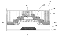
이어서, 도 21을 참조하여, 본 발명의 실시 형태 7에 따른 TFT(10)의 구성을 설명한다. 도 21은 실시 형태 7에 따른 TFT(10)의 단면을 모식적으로 나타내고 있다.Next, with reference to FIG. 21, the structure of the
실시 형태 7의 TFT(10)는, 기판(60) 위에 형성된 게이트 전극(62)과, 게이트 전극(62) 위에 형성된 게이트 절연층(66)과, 게이트 절연층(66) 위에 형성된 산화물 반도체층(68)과, 산화물 반도체층(68) 위에 배치된 소스 전극(70s) 및 드레인 전극(70d)과, 소스 전극(70s) 및 드레인 전극(70d) 위에 형성된 보호층(72)과, 보호층(72) 위에 형성된 산소 공급층(74)과, 산소 공급층 위에 형성된 확산 방지층(78)을 구비하고 있다. 이 TFT(10)는, 실시 형태 1의 TFT(10)에서의 보호층(72)에 콘택트 홀(72h)이 형성된 형태를 갖는다. 또한, 이 형태는, 실시 형태 5에 확산 방지층(78)을 부가한 형태이기도 하다.The
콘택트 홀(72h)은 산소 공급층(74)에 의해 매립되어 있으며, 콘택트 홀(72h)의 저부에서 산소 공급층(74)이 산화물 반도체층(68)에 접하고 있다. 산소 공급층(74)과 산화물 반도체층(68)이 채널부 근방에서 접하고 있기 때문에, 실시 형태 1보다도 산화물 반도체층(68)에 보다 많은 H2O 등을 보충할 수 있다. 또한, 실시 형태 4와 같이, 산화물 반도체층(68)의 채널부에 직접 산소 공급층(74)이 접하는 경우, 채널부의 상면 부근에 많은 불순물이 혼입되는 등의 문제가 발생할 우려가 있다. 그러나, 본 실시 형태에서는, 채널부 위에 보호층(72)이 형성되어 있기 때문에, 그러한 문제가 방지되어, TFT의 신뢰성이 향상된다. 또한 본 형태에 의하면, 확산 방지층(78)에 의한 효과도 얻을 수 있다.The
도 22는, 본 실시 형태에 따른 복수의 TFT(10)의 전압-전류 특성을 나타낸 그래프이며, 횡축은 게이트 전압값을, 종축은 소스-드레인 전류값을 각각 나타내고 있다. 도 6의 (a)는 보호층(72)이 콘택트 홀(72h)을 갖지 않고, 산화물 반도체층(68)과 산소 공급층(74)이 직접 접하는 경우가 없는 실시 형태 1의 특성을 나타내고 있다. 도 6의 (a)와 도 22를 비교하여 알 수 있는 바와 같이, 실시 형태 7의 TFT(10)에서는, 실시 형태 1의 TFT(10)보다도, 게이트 전압 0V 부근에서의 전류의 상승이 보다 급격하면서, 복수의 TFT(10)의 특성(S값)에 변동이 적다. 이것은, 실시 형태 7에 의하면, 복수의 TFT(10)에서, ON시부터 인가 전압에 따른 보다 적절한 전류값이, 보다 변동 적게 얻어지는 것을 나타내고 있다. 이들 비교로부터, 산화물 반도체층(68)과 산소 공급층(74)이 직접 접함으로써, 보다 TFT 특성이 안정된 고성능의 반도체 장치가 얻어지는 것을 알 수 있다.22 is a graph showing the voltage-current characteristics of the plurality of
이어서, 도 23 내지 도 28을 참조하여 본 발명에 따른 실시 형태 8 내지 13을 설명한다. 이들 실시 형태에서는, 각 TFT(10)가 산소 공급층(74) 위에 확산 방지층(78)이 배치되는 것으로서 설명하고 있지만, 확산 방지층(78)을 구비하지 않는 형태도 있을 수 있다.Next, Embodiments 8 to 13 according to the present invention will be described with reference to FIGS. 23 to 28. In these embodiments, the
(실시 형태 8)(Embodiment 8)
우선, 도 23을 참조하여, 본 발명의 실시 형태 8에 따른 TFT(10)의 구성을 설명한다. 도 23은, 실시 형태 8에 따른 TFT(10)의 단면을 모식적으로 나타내고 있다.First, with reference to FIG. 23, the structure of the
실시 형태 8의 TFT(10)는, 기판(60) 위에 형성된 게이트 전극(62)과, 게이트 전극(62) 위에 형성된 게이트 절연층(66)과, 게이트 절연층(66) 위에 형성된 산화물 반도체층(68)과, 산화물 반도체층(68) 위에 배치된 소스 전극(70s) 및 드레인 전극(70d)과, 소스 전극(70s) 및 드레인 전극(70d) 위에 형성된 보호층(72)과, 보호층(72) 위에 형성된 산소 공급층(74)과, 산소 공급층(74) 위에 형성된 확산 방지층(78)을 구비하고 있다.The
이 TFT(10)는, 실시 형태 1의 TFT(10)와 동일한 구성을 갖는다. 단, 본 실시 형태의 보호층(72)은 실시 형태 1의 보호층(72)보다도 낮은 밀도를 갖는다. 보호층(72)의 밀도는, 예를 들어 실시 형태 1에서는, 2.2g/㎤이며, 실시 형태 8에서는 2.0g/㎤이다. 실시 형태 8의 보호층(72)의 밀도는 1.9 내지 2.2g/㎤의 범위 내에 있는 것이 바람직하다. 보다 낮은 밀도를 가짐으로써, 실시 형태 1의 보호층(72)보다도 H2O 등의 투과율이 높아져서, 보다 많은 채널부의 결함을 보완할 수 있다.This
(실시 형태 9)(Embodiment 9)
이어서, 도 24를 참조하여, 본 발명의 실시 형태 9에 따른 TFT(10)의 구성을 설명한다. 도 24는, 실시 형태 9에 따른 TFT(10)의 단면을 모식적으로 나타내고 있다.Next, with reference to FIG. 24, the structure of the
실시 형태 9의 TFT(10)는, 기판(60) 위에 형성된 게이트 전극(62)과, 게이트 전극(62) 위에 형성된 게이트 절연층(66)과, 게이트 절연층(66) 위에 형성된 산화물 반도체층(68)과, 산화물 반도체층(68) 위에 배치된 소스 전극(70s) 및 드레인 전극(70d)과, 소스 전극(70s) 및 드레인 전극(70d) 위에 형성된 제1 보호층(72a)과, 제1 보호층(72a) 위에 형성된 제2 보호층(72b)과, 제2 보호층(72b) 위에 형성된 산소 공급층(74)과, 산소 공급층(74) 위에 형성된 확산 방지층(78)을 구비하고 있다.The
이 TFT(10)는, 보호층(72)이 제1 보호층(72a)과 제2 보호층(72b)에 의한 2층 구성으로 되어 있는 이외에는, 실시 형태 1의 TFT(10)와 동일한 구성을 갖는다. 제1 보호층(72a)은 제2 보호층(72b)보다도 높은 밀도를 갖는다.This
제1 보호층(72a)의 밀도는, 예를 들어 2.2g/㎤이며, 제2 보호층(72b)의 밀도는, 예를 들어 2.0g/㎤이다. 제1 보호층(72a)의 밀도는 2.1 내지 2.4g/㎤의 범위 내에 있는 것이 바람직하며, 제2 보호층(72b)의 밀도는 1.9 내지 2.2g/㎤의 범위 내에 있는 것이 바람직하다.The density of the first
산화물 반도체층(68)과 접하는 제1 보호층(72a)을 저밀도로 하면, 보호층으로서의 신뢰성이 저하된다. 본 실시 형태에서는, 보호층(72)의 특히 중요한 산화물 반도체층(68) 계면 부근의 부분(산화물 반도체층(68)의 계면으로부터 5 내지 25㎚의 두께 부분)을 고밀도막으로 하고, 제2 보호층(72b)을 저밀도막으로 함으로써, 보호막으로서의 기능과 H2O, OR기 또는 OH기를 적당히 투과하는 성질을 모두 보호층(72)에 제공하고 있다.When the first
(실시 형태 10)(Embodiment 10)
이어서, 도 25를 참조하여, 본 발명의 실시 형태 10에 따른 TFT(10)의 구성을 설명한다. 도 25는, 실시 형태 10에 따른 TFT(10)의 단면을 모식적으로 나타내고 있다.Next, with reference to FIG. 25, the structure of the
실시 형태 10의 TFT(10)는, 기판(60) 위에 형성된 게이트 전극(62)과, 게이트 전극(62) 위에 형성된 게이트 절연층(66)과, 게이트 절연층(66) 위에 형성된 산화물 반도체층(68)과, 산화물 반도체층(68) 위에 배치된 에칭 스토퍼층(97: ES층)과, 소스 전극(70s) 및 드레인 전극(70d)과, ES층(97), 소스 전극(70s) 및 드레인 전극(70d) 위에 형성된 보호층(72)과, 보호층(72) 위에 형성된 산소 공급층(74)과, 산소 공급층(74) 위에 형성된 확산 방지층(78)을 구비하고 있다.The
ES층(97)은 산화물 반도체층(68)의 채널부 위의, 소스 전극(70s)과 드레인 전극(70d)의 단부에 끼워진 위치에 배치되어 있다. ES층(97)의 양단부 위에는, 각각 소스 전극(70s) 및 드레인 전극(70d)의 단부가 형성되어 있으며, ES층(97)의 중앙부의 상면은 보호층(72)에 접하고 있다. ES층(97)은 실리콘 산화막 또는 실리콘 산화막과 실리콘 질화막의 적층막(상층이 실리콘 질화막)에 의해 형성되어 있다. 여기에서는 실리콘 산화막의 두께를 100㎚로 하였다. ES층(97)이 배치됨으로써, 소스 전극(70s) 및 드레인 전극(70d)으로 되는 메탈층을 에칭할 때의 에칭 대미지로부터 산화물 반도체층(68)의 채널부를 보호할 수 있다. 따라서, 보다 특성이 안정된 신뢰성이 높은 TFT를 제작할 수 있다.The
(실시 형태 11)(Embodiment 11)
이어서, 도 26을 참조하여, 본 발명의 실시 형태 11에 따른 TFT(10)의 구성을 설명한다. 도 26은, 실시 형태 11에 따른 TFT(10)의 단면을 모식적으로 나타내고 있다.Next, with reference to FIG. 26, the structure of the
실시 형태 11의 TFT(10)는, 기판(60) 위에 형성된 게이트 전극(62)과, 게이트 전극(62) 위에 형성된 게이트 절연층(66)과, 게이트 절연층(66) 위에 형성된 산화물 반도체층(68)과, 산화물 반도체층(68) 위에 배치된 ES층(97), 소스 전극(70s) 및 드레인 전극(70d)과, ES층(97), 소스 전극(70s) 및 드레인 전극(70d) 위에 형성된 산소 공급층(74)과, 산소 공급층(74) 위에 형성된 확산 방지층(78)을 구비하고 있다.The
실시 형태 10은 보호층(72)이 형성되어 있지 않은 점에서 서로 다르지만, 다른 구성은 동일하다. 산화물 반도체층(68)의 채널부에 산소 공급층(74)이 ES층(97)만을 통하여 접하고 있기 때문에, H2O 등의 채널부에의 이동이 용이해져서, 채널부의 결함을 효율적으로 보완할 수 있다.The tenth embodiment differs from the other in that the
실시 형태 10 및 11에서는, TFT(10)가 ES층(97)을 갖는 2가지 형태를 설명하였지만, 이것에 한정되지 않고, 전술한 실시 형태 1 내지 9의 채널층 위에 ES층(97)이 배치된 형태도 본원 발명의 실시 형태에 포함될 수 있다.In the tenth and eleventh embodiments, the two modes in which the
(실시 형태 12)(Embodiment 12)
이어서, 도 27을 참조하여, 본 발명의 실시 형태 12에 따른 TFT(10)의 구성을 설명한다. 도 27은, 실시 형태 12에 따른 TFT(10)의 단면을 모식적으로 나타내고 있다.Next, with reference to FIG. 27, the structure of
실시 형태 12의 TFT(10)는, 기판(60) 위에 형성된 게이트 전극(62)과, 게이트 전극(62) 위에 형성된 게이트 절연층(66)과, 게이트 절연층(66) 위에 형성된 소스 전극(70s) 및 드레인 전극(70d)과, 소스 전극(70s) 및 드레인 전극(70d) 위에 형성된 산화물 반도체층(68)과, 산화물 반도체층(68) 위에 배치된 보호층(72)과, 보호층(72) 위에 형성된 산소 공급층(74)과, 산소 공급층(74) 위에 형성된 확산 방지층(78)을 구비하고 있다.The
여기에서는, 소스 전극(70s) 및 드레인 전극(70d)은 게이트 절연층(66)과 산화물 반도체층(68) 사이에 형성된다. 단, 소스 전극(70s) 및 드레인 전극(70d)의 단부에 끼워진 산화물 반도체층(68)의 채널부는, 그 하면이 게이트 절연층(66)의 상면과 직접 접하도록 형성되어 있다.Here, the
이 구성에 의하면, 산화물 반도체층(68)이 소스 전극(70s) 및 드레인 전극(70d)을 끼우지 않고, 보호층(72)만을 통하여 산소 공급층(74)에 접하므로, H2O 등의 산화물 반도체층(68)으로의 이동이 용이해져서, 산화물 반도체층(68)의 결함을 보다 많이 보완할 수 있다.According to this configuration, since the
(실시 형태 13)(Embodiment 13)
이어서, 도 28을 참조하여, 본 발명의 실시 형태 13에 따른 TFT(10)의 구성을 설명한다. 도 28은, 실시 형태 13에 따른 TFT(10)의 단면을 모식적으로 나타내고 있다.Next, with reference to FIG. 28, the structure of
실시 형태 13의 TFT(10)는 톱 게이트형 TFT이며, 기판(60) 위에 형성된 소스 전극(70s) 및 드레인 전극(70d)과, 소스 전극(70s) 및 드레인 전극(70d) 위에 형성된 산화물 반도체층(68)과, 산화물 반도체층(68) 위에 형성된 게이트 절연층(66)과, 게이트 절연층(66) 위에 형성된 게이트 전극(62)과, 게이트 전극(62) 위에 형성된 산소 공급층(74)과, 산소 공급층(74) 위에 형성된 확산 방지층(78)을 구비하고 있다.The
산화물 반도체층(68)의, 소스 전극(70s) 및 드레인 전극(70d)의 단부에 끼워진 채널부는 기판(60)에 접하도록 형성되고, 그 밖의 부분은 소스 전극(70s) 또는 드레인 전극(70d) 위에 형성된다. 게이트 전극(62)은 산화물 반도체층(68)의 중앙 상부에 배치되고, 게이트 전극(62)이 형성되어 있지 않은 부분에서는, 게이트 절연층(66)과 산소 공급층(74)이 직접 접하고 있다.The channel portion of the
이 구성에 의하면, 게이트 절연층(66)을 통하여, 산소 공급층(74)으로부터 산화물 반도체층(68)으로 H2O 등이 이동하기 때문에, 산화물 반도체층(68)의 결함을 보완할 수 있다. 또한, 소스 전극(70s) 및 드레인 전극(70d)이 확산 방지층으로서의 역할을 완수하므로, 보다 효과적으로 결함이 보완된다.According to this configuration, since H 2 O or the like moves from the
(실시 형태 14)(Embodiment 14)
이어서, 본 발명의 실시 형태 14에 따른 유기 EL 표시 장치(1002)를 설명한다.Next, the organic
도 29는, 유기 EL 표시 장치(1002)(단순히 '표시 장치(1002)'라고도 함)의 구성을 모식적으로 나타낸 단면도이다. 도 29에 도시한 바와 같이, 표시 장치(1002)는 TFT 기판(140)과, TFT 기판(140) 위에 형성된 홀 수송층(144)과, 홀 수송층(144) 위에 형성된 발광층(146)과, 발광층(146) 위에 설치된 대향 전극(148)을 구비하고 있다. 홀 수송층(144)과 발광층(146)은 유기 EL층을 구성한다. 유기 EL층은 절연성 돌기(147)에 의해 구분되어 있으며, 구분된 유기 EL층이 1개의 화소의 유기 EL층을 이룬다.29 is a cross-sectional view schematically showing the configuration of an organic EL display device 1002 (also referred to simply as a 'display device 1002'). As shown in FIG. 29, the
TFT 기판(140)은 전술한 실시 형태의 TFT 기판(100)과 기본적으로 동일한 구성을 가지며, 기판(60) 위에 형성된 TFT(10)를 구비하고 있다. TFT(10)에는, 실시 형태 1 내지 13에서 설명한 TFT(10)가 이용될 수 있다. TFT 기판(140)은 TFT(10)를 덮어 적층된 층간 절연층(74) 및 층간 절연층(74) 위에 형성된 화소 전극(109)을 갖는다. 화소 전극(109)은 층간 절연층(74)에 형성된 콘택트 홀 내에서 TFT(10)의 드레인 전극에 접속되어 있다. TFT 기판(140)의 평면 구성은, 도 2 및 도 3에 도시한 것과 기본적으로 동일하므로, 그 설명을 생략한다. 또한, TFT 기판(140)으로서, 보조 용량을 갖지 않는 형태를 이용해도 된다.The
화소 전극(109) 및 대향 전극(148)에 의해 유기 EL층에 전압이 인가되면, 홀 수송층(144)을 통하여 화소 전극(109)으로부터 발생한 홀이 발광층(146)으로 보내진다. 또한 동시에, 발광층(146)에는 대향 전극(148)으로부터 발생한 전자가 이동하고, 그와 같은 홀과 전자가 재결합됨으로써 발광층(146) 내에서 발광이 일어난다. 발광층(146)에서의 발광을, 액티브 매트릭스 기판인 TFT 기판(140)을 이용하여 화소마다 제어함으로써, 원하는 표시가 이루어진다.When a voltage is applied to the organic EL layer by the
홀 수송층(144), 발광층(146) 및 대향 전극(148)의 재료와, 이들 층 구조에는, 공지된 재료 및 구조를 이용해도 된다. 홀 수송층(144)과 발광층(146) 사이에, 홀 주입 효율을 높이기 위해서, 홀 주입층을 형성할 수도 있다. 광의 출사 효율을 높이는 동시에, 유기 EL층으로의 높은 전자 주입 효율을 달성하기 위해서, 대향 전극(148)에는 투과율이 높으면서, 일함수가 작은 재료를 이용하는 것이 바람직하다.A well-known material and structure may be used for the material of the
본 실시 형태의 유기 EL 표시 장치(1002)는 실시 형태 1 내지 13에서 설명한 TFT(10)를 이용하고 있기 때문에, 실시 형태 1 내지 13에서 설명한 것과 마찬가지의 효과를 얻을 수 있다. 본 실시 형태에 의하면, 고성능 표시를 행할 수 있는 유기 EL 표시 장치(1002)를 제조 효율 좋게 제공하는 것이 가능해진다.Since the organic
본 발명은 박막 트랜지스터를 갖는 반도체 장치 및 박막 트랜지스터를 TFT 기판에 구비한 액정 표시 장치, 유기 EL 표시 장치 등의 표시 장치에 알맞게 이용된다.INDUSTRIAL APPLICABILITY The present invention is suitably used for a display device such as a liquid crystal display device and an organic EL display device having a thin film transistor and a thin film transistor provided on a TFT substrate.
10: TFT(박막 트랜지스터)
12: 신호선
14: 주사선
16: 보조 용량선
18: 보조 용량(Cs)
20: 화소 전극
20c: 보조 용량 대향 전극
20t, 22: 도전층
25: 접속부
30: 단자부
50: 화소
60: 기판
62: 게이트 전극
62c: 보조 용량 전극
62d: 하부 배선
66: 게이트 절연층
68: 산화물 반도체층
68m: 산화물 반도체 재료
70d: 드레인 전극
70s: 소스 전극
70u: 상부 배선
72: 보호층
72h: 콘택트 홀
74: 산소 공급층
78: 확산 방지층
90: 공통선
92: 하층 전극
94: 상층 전극
97: ES층
100: TFT 기판(반도체 장치)
200: 대향 기판
210, 220: 편광판
230: 백라이트 유닛
240: 주사선 구동 회로
250: 신호선 구동 회로
260: 제어 회로
1000: 액정 표시 장치
1002: 유기 EL 표시 장치10: TFT (Thin Film Transistor)
12: signal line
14: scanning line
16: auxiliary capacitance line
18: auxiliary capacity (Cs)
20: pixel electrode
20c: storage capacitor counter electrode
20t, 22: conductive layer
25: connection
30: terminal portion
50: pixel
60: substrate
62: gate electrode
62c: storage capacitor electrode
62d: bottom wiring
66: gate insulating layer
68: oxide semiconductor layer
68m: oxide semiconductor material
70d: drain electrode
70s: source electrode
70u: upper wiring
72: protective layer
72h: contact hall
74: oxygen supply layer
78: diffusion barrier layer
90: common line
92: lower electrode
94: upper electrode
97: ES layer
100: TFT substrate (semiconductor device)
200: counter substrate
210, 220: polarizer
230: backlight unit
240: scan line driving circuit
250: signal line driver circuit
260: control circuit
1000: liquid crystal display
1002: organic EL display device
Claims (29)
기판 위에 형성된, 상기 박막 트랜지스터의 게이트 전극과,
상기 게이트 전극 위에 형성된 게이트 절연층과,
상기 게이트 절연층 위에 형성된 산화물 반도체층과,
상기 산화물 반도체층 위에 형성된, 상기 박막 트랜지스터의 소스 전극 및 드레인 전극과,
상기 산화물 반도체층, 상기 소스 전극 및 상기 드레인 전극 위에 형성된 보호층과,
상기 보호층 위에 형성된 산소 공급층과,
상기 산소 공급층 위에 형성된 확산 방지층
을 구비한, 반도체 장치.A semiconductor device comprising a thin film transistor,
A gate electrode of the thin film transistor formed on a substrate;
A gate insulating layer formed on the gate electrode;
An oxide semiconductor layer formed on the gate insulating layer;
A source electrode and a drain electrode of the thin film transistor formed on the oxide semiconductor layer;
A protective layer formed on the oxide semiconductor layer, the source electrode and the drain electrode;
An oxygen supply layer formed on the protective layer,
Diffusion barrier layer formed on the oxygen supply layer
And a semiconductor device.
상기 산소 공급층이, 물(H2O), OR기 또는 OH기를 함유하는 재료를 포함하여 이루어지는 층인, 반도체 장치.The method of claim 1,
A semiconductor device, wherein the oxygen supply layer is a layer containing a material containing water (H 2 O), an OR group, or an OH group.
상기 산소 공급층이, 아크릴 수지, SOG 재료, 실리콘 수지, 에스테르 중합 수지, 또는 실라놀기, CO-OR기 또는 Si-OH기를 함유하는 수지를 포함하여 이루어지는, 반도체 장치.3. The method according to claim 1 or 2,
The semiconductor device in which the said oxygen supply layer contains acrylic resin, SOG material, silicone resin, ester polymerization resin, or resin containing a silanol group, a CO-OR group, or a Si-OH group.
상기 산소 공급층의 두께가 500㎚ 내지 3500㎚의 범위에 있는, 반도체 장치.4. The method according to any one of claims 1 to 3,
And the thickness of the oxygen supply layer is in the range of 500 nm to 3500 nm.
상기 확산 방지층이, 산화실리콘, 질화실리콘 또는 산질화실리콘을 포함하여 이루어지는, 반도체 장치.5. The method according to any one of claims 1 to 4,
A semiconductor device, wherein the diffusion barrier layer comprises silicon oxide, silicon nitride, or silicon oxynitride.
상기 확산 방지층의 두께가 50㎚ 내지 500㎚의 범위에 있는, 반도체 장치.The method according to any one of claims 1 to 5,
A semiconductor device, wherein the diffusion barrier layer has a thickness in a range of 50 nm to 500 nm.
상기 보호층이, 산화실리콘 또는 질화실리콘을 포함하여 이루어지는, 반도체 장치.7. The method according to any one of claims 1 to 6,
The semiconductor device in which the said protective layer contains silicon oxide or silicon nitride.
상기 게이트 전극과 동일한 재료로 형성된 하부 배선과,
상기 소스 전극 및 상기 드레인 전극과 동일한 재료로 형성된 상부 배선과,
상기 상부 배선과 상기 하부 배선이 접속된 접속부를 구비하고,
상기 접속부에서, 상기 상부 배선과 상기 하부 배선이, 상기 게이트 절연층을 관통하는 콘택트 홀을 통하여 접속되어 있는, 반도체 장치.8. The method according to any one of claims 1 to 7,
A lower wiring formed of the same material as the gate electrode,
An upper wiring formed of the same material as the source electrode and the drain electrode;
A connection portion to which the upper wiring and the lower wiring are connected;
In the connecting portion, the upper wiring and the lower wiring are connected through a contact hole passing through the gate insulating layer.
상기 접속부에서, 상기 콘택트 홀이 산화물 반도체층과 상기 게이트 절연층을 관통하도록 형성되어 있으며, 상기 상부 배선과 상기 하부 배선이, 상기 콘택트 홀을 통하여 접속되어 있는, 반도체 장치.9. The method of claim 8,
The semiconductor device, wherein the contact hole is formed to penetrate the oxide semiconductor layer and the gate insulating layer, and the upper wiring and the lower wiring are connected through the contact hole.
상기 접속부는,
상기 하부 배선 위에 형성된 절연층과,
상기 절연층 위에 형성된 상부 배선과,
상기 상부 배선 위에 형성된 보호층과,
상기 보호층 위에 형성된 산소 공급층과,
상기 산소 공급층 위에 형성된 확산 방지층과,
상기 확산 방지층 위에 형성된 도전층을 갖고,
상기 접속부의 상기 절연층, 상기 상부 배선, 상기 보호층, 상기 산소 공급층 및 상기 확산 방지층을 관통하도록 콘택트 홀이 형성되어 있으며,
상기 콘택트 홀 내에 형성된 상기 도전층을 통하여, 상기 하부 배선과 상기 상부 배선이 전기적으로 접속되어 있는, 반도체 장치.9. The method of claim 8,
Wherein the connecting portion comprises:
An insulating layer formed on the lower interconnection,
An upper wiring formed on the insulating layer,
A protective layer formed on the upper wiring;
An oxygen supply layer formed on the protective layer,
A diffusion barrier layer formed on the oxygen supply layer,
It has a conductive layer formed on the said diffusion prevention layer,
A contact hole is formed to penetrate the insulating layer, the upper wiring, the protective layer, the oxygen supply layer, and the diffusion barrier layer of the connection part;
The lower wiring and the upper wiring are electrically connected to each other through the conductive layer formed in the contact hole.
상기 접속부는,
상기 하부 배선 위에 형성된 절연층과,
상기 절연층 위에 형성된 상기 상부 배선과,
상기 상부 배선 위에 형성된 보호층과,
상기 보호층 위에 형성된 산소 공급층과,
상기 산소 공급층 위에 형성된 확산 방지층과,
상기 확산 방지층 위에 형성된 도전층을 갖고,
상기 접속부의 상기 보호층, 상기 산소 공급층 및 상기 확산 방지층을 관통하도록 제1 콘택트 홀이 형성되어 있으며,
상기 접속부의 상기 절연층, 상기 보호층, 상기 산소 공급층 및 상기 확산 방지층을 관통하도록 제2 콘택트 홀이 형성되어 있으며,
상기 제1 콘택트 홀 내에서 상기 상부 배선과 상기 도전층이 전기적으로 접속되어 있고,
상기 제2 콘택트 홀 내에서 상기 하부 배선과 상기 도전층이 전기적으로 접속되어 있는, 반도체 장치.9. The method of claim 8,
Wherein the connecting portion comprises:
An insulating layer formed on the lower interconnection,
The upper wiring formed on the insulating layer,
A protective layer formed on the upper wiring;
An oxygen supply layer formed on the protective layer,
A diffusion barrier layer formed on the oxygen supply layer,
It has a conductive layer formed on the said diffusion prevention layer,
A first contact hole is formed to penetrate the protective layer, the oxygen supply layer, and the diffusion barrier layer of the connection part,
A second contact hole is formed to penetrate the insulating layer, the protective layer, the oxygen supply layer, and the diffusion barrier layer of the connection part,
The upper wiring and the conductive layer are electrically connected in the first contact hole,
And the lower wiring and the conductive layer are electrically connected in the second contact hole.
상기 게이트 전극과 동일한 재료에 의한 보조 용량 전극과,
상기 보조 용량 전극 위에 상기 보조 용량 전극에 접하도록 형성된 상기 확산 방지층과,
상기 확산 방지층 위에 형성된 보조 용량 대향 전극
을 갖는 보조 용량을 구비한, 반도체 장치.12. The method according to any one of claims 1 to 11,
A storage capacitor electrode made of the same material as the gate electrode;
The diffusion barrier layer formed on the storage capacitor electrode and in contact with the storage capacitor electrode;
A storage capacitor counter electrode formed on the diffusion barrier layer
A semiconductor device having a storage capacitor having a.
상기 게이트 전극과 동일한 재료에 의한 보조 용량 전극과,
상기 보조 용량 전극 위에 상기 보조 용량 전극에 접하도록 형성된 제1 도전층과,
상기 제1 도전층 위에 상기 제1 도전층에 접하도록 형성된 상기 확산 방지층과,
상기 확산 방지층 위에 형성된 보조 용량 대향 전극
을 갖는 보조 용량을 구비한, 반도체 장치.12. The method according to any one of claims 1 to 11,
A storage capacitor electrode made of the same material as the gate electrode;
A first conductive layer formed on the storage capacitor electrode and in contact with the storage capacitor electrode;
The diffusion barrier layer formed on the first conductive layer to contact the first conductive layer;
A storage capacitor counter electrode formed on the diffusion barrier layer
A semiconductor device having a storage capacitor having a.
상기 게이트 전극과 동일한 재료에 의한 보조 용량 전극과,
상기 보조 용량 전극 위에 상기 보조 용량 전극에 접하도록 형성된 산화물 반도체층과,
상기 보조 용량 전극 위의 상기 산화물 반도체층에 접하도록 형성된 상기 확산 방지층과,
상기 확산 방지층 위에 형성된 보조 용량 대향 전극
을 갖는 보조 용량을 구비한, 반도체 장치.12. The method according to any one of claims 1 to 11,
A storage capacitor electrode made of the same material as the gate electrode;
An oxide semiconductor layer formed on the storage capacitor electrode and in contact with the storage capacitor electrode;
The diffusion barrier layer formed to contact the oxide semiconductor layer on the storage capacitor electrode;
A storage capacitor counter electrode formed on the diffusion barrier layer
A semiconductor device having a storage capacitor having a.
상기 확산 방지층 위에 형성된 화소 전극을 구비하고,
상기 화소 전극이, 상기 보호층, 상기 산소 공급층 및 상기 확산 방지층을 관통하는 콘택트 홀을 통하여 상기 드레인 전극에 접속되어 있는, 표시 장치.A display device comprising the semiconductor device according to any one of claims 1 to 14.
A pixel electrode formed on the diffusion barrier layer;
And the pixel electrode is connected to the drain electrode through a contact hole penetrating through the protective layer, the oxygen supply layer, and the diffusion barrier layer.
상기 산소 공급층과 상기 확산 방지층 사이에 배치된 하층 전극과,
상기 확산 방지층 위에 배치되고, 상기 박막 트랜지스터의 상기 드레인 전극에 접속된 상층 전극을 구비한 프린지 필드형 표시 장치.A display device comprising the semiconductor device according to any one of claims 1 to 14.
A lower electrode disposed between the oxygen supply layer and the diffusion barrier layer;
A fringe field type display device disposed on the diffusion barrier layer and having an upper electrode connected to the drain electrode of the thin film transistor.
상기 게이트 전극과 동일한 재료에 의해 형성된 공통선을 구비하고,
상기 공통선과 상기 하층 전극이, 상기 게이트 절연층, 상기 보호층 및 상기 산소 공급층을 관통하는 콘택트 홀을 통하여 접속되어 있는 프린지 필드형 표시 장치.17. The method of claim 16,
A common line formed of the same material as the gate electrode,
A fringe field type display device, wherein the common line and the lower electrode are connected through a contact hole penetrating through the gate insulating layer, the protective layer, and the oxygen supply layer.
상기 보호층의 밀도가 1.9 내지 2.2g/㎤의 범위 내에 있는, 반도체 장치.8. The method according to any one of claims 1 to 7,
And the density of the protective layer is in the range of 1.9 to 2.2 g / cm 3.
상기 보호층이, 상기 산화물 반도체층, 상기 소스 전극 및 상기 드레인 전극 위에 형성된 제1 보호층 및 상기 제1 보호층 위에 형성된, 상기 제1 보호층보다도 밀도가 낮은 제2 보호층을 포함하여 이루어지는, 반도체 장치.8. The method according to any one of claims 1 to 7,
The protective layer comprises a first protective layer formed on the oxide semiconductor layer, the source electrode and the drain electrode, and a second protective layer having a lower density than the first protective layer formed on the first protective layer, Semiconductor device.
상기 제1 보호층의 밀도가 2.1 내지 2.4g/㎤의 범위 내에 있고, 상기 제2 보호층의 밀도가 1.9 내지 2.2g/㎤의 범위 내에 있는, 반도체 장치.20. The method of claim 19,
And the density of the first protective layer is in the range of 2.1 to 2.4 g / cm 3, and the density of the second protective layer is in the range of 1.9 to 2.2 g / cm 3.
상기 산화물 반도체층과 상기 소스 전극 및 상기 드레인 전극 사이에 형성된 에칭 스토퍼층을 구비한, 반도체 장치.8. The method according to any one of claims 1 to 7,
And an etching stopper layer formed between said oxide semiconductor layer and said source electrode and said drain electrode.
기판 위에 형성된, 상기 박막 트랜지스터의 게이트 전극과,
상기 게이트 전극 위에 형성된 게이트 절연층과,
상기 게이트 절연층 위에 형성된 산화물 반도체층과,
상기 산화물 반도체층 위에 배치된, 상기 박막 트랜지스터의 소스 전극 및 드레인 전극과,
상기 산화물 반도체층, 상기 소스 전극 및 상기 드레인 전극 위에 상기 산화물 반도체층에 접하도록 형성된 산소 공급층
을 구비한, 반도체 장치.A semiconductor device comprising a thin film transistor,
A gate electrode of the thin film transistor formed on a substrate;
A gate insulating layer formed on the gate electrode;
An oxide semiconductor layer formed on the gate insulating layer;
A source electrode and a drain electrode of the thin film transistor disposed on the oxide semiconductor layer;
An oxygen supply layer formed to contact the oxide semiconductor layer on the oxide semiconductor layer, the source electrode and the drain electrode
And a semiconductor device.
상기 산화물 반도체층, 상기 소스 전극 및 상기 드레인 전극과 상기 산소 공급층 사이에 배치된 보호층을 구비하고,
상기 산소 공급층이, 상기 보호층에 형성된 콘택트 홀을 통하여, 상기 산화물 반도체층에 접하고 있는, 반도체 장치.24. The method of claim 23,
A protective layer disposed between the oxide semiconductor layer, the source electrode, the drain electrode, and the oxygen supply layer,
The semiconductor device, wherein the oxygen supply layer is in contact with the oxide semiconductor layer via a contact hole formed in the protective layer.
상기 산소 공급층 위에 형성된 확산 방지층을 구비하는, 반도체 장치.25. The method according to claim 23 or 24,
And a diffusion barrier layer formed on the oxygen supply layer.
상기 산화물 반도체층과 상기 소스 전극 및 상기 드레인 전극 사이에 형성된 에칭 스토퍼층을 구비한, 반도체 장치.24. The method of claim 23,
And an etching stopper layer formed between said oxide semiconductor layer and said source electrode and said drain electrode.
기판 위에 형성된, 상기 박막 트랜지스터의 게이트 전극과,
상기 게이트 전극 위에 형성된 게이트 절연층과,
상기 게이트 절연층 위에 형성된, 상기 박막 트랜지스터의 소스 전극 및 드레인 전극과,
상기 게이트 절연층, 상기 소스 전극 및 상기 드레인 전극 위에 형성된 산화물 반도체층과,
상기 산화물 반도체층 위에 형성된 보호층과,
상기 보호층 위에 형성된 산소 공급층
을 구비한, 반도체 장치.A semiconductor device comprising a thin film transistor,
A gate electrode of the thin film transistor formed on a substrate;
A gate insulating layer formed on the gate electrode;
A source electrode and a drain electrode of the thin film transistor formed on the gate insulating layer;
An oxide semiconductor layer formed on the gate insulating layer, the source electrode and the drain electrode;
A protective layer formed on the oxide semiconductor layer;
An oxygen supply layer formed on the protective layer
And a semiconductor device.
기판 위에 형성된, 상기 박막 트랜지스터의 소스 전극 및 드레인 전극과,
상기 소스 전극 및 상기 드레인 전극 위에 형성된 산화물 반도체층과,
상기 산화물 반도체층, 상기 소스 전극 및 상기 드레인 전극 위에 형성된 절연층과,
상기 절연층 위에 형성된, 상기 박막 트랜지스터의 게이트 전극과,
상기 절연층 및 상기 게이트 전극 위에 형성된 산소 공급층과,
상기 산소 공급층 위에 형성된 확산 방지층
을 구비한, 반도체 장치.A top gate semiconductor device comprising a thin film transistor,
A source electrode and a drain electrode of the thin film transistor formed on a substrate,
An oxide semiconductor layer formed on the source electrode and the drain electrode;
An insulating layer formed on the oxide semiconductor layer, the source electrode and the drain electrode;
A gate electrode of the thin film transistor formed on the insulating layer;
An oxygen supply layer formed on the insulating layer and the gate electrode;
Diffusion barrier layer formed on the oxygen supply layer
And a semiconductor device.
Applications Claiming Priority (3)
| Application Number | Priority Date | Filing Date | Title |
|---|---|---|---|
| JPJP-P-2010-282919 | 2010-12-20 | ||
| JP2010282919 | 2010-12-20 | ||
| PCT/JP2011/079036 WO2012086513A1 (en) | 2010-12-20 | 2011-12-15 | Semiconductor device and display device |
Publications (2)
| Publication Number | Publication Date |
|---|---|
| KR20140003481A true KR20140003481A (en) | 2014-01-09 |
| KR101630503B1 KR101630503B1 (en) | 2016-06-14 |
Family
ID=46313789
Family Applications (1)
| Application Number | Title | Priority Date | Filing Date |
|---|---|---|---|
| KR1020137018856A Active KR101630503B1 (en) | 2010-12-20 | 2011-12-15 | Semiconductor device and display device |
Country Status (6)
| Country | Link |
|---|---|
| US (2) | US20150108467A1 (en) |
| EP (1) | EP2657974B1 (en) |
| JP (1) | JP5284544B2 (en) |
| KR (1) | KR101630503B1 (en) |
| CN (1) | CN103270601B (en) |
| WO (1) | WO2012086513A1 (en) |
Cited By (1)
| Publication number | Priority date | Publication date | Assignee | Title |
|---|---|---|---|---|
| KR20150110340A (en) * | 2014-03-20 | 2015-10-02 | 가부시키가이샤 한도오따이 에네루기 켄큐쇼 | Semiconductor device, display device including semiconductor device, display module including display device, and electronic device including semiconductor device, display device, and display module |
Families Citing this family (73)
| Publication number | Priority date | Publication date | Assignee | Title |
|---|---|---|---|---|
| US8679905B2 (en) * | 2011-06-08 | 2014-03-25 | Cbrite Inc. | Metal oxide TFT with improved source/drain contacts |
| WO2013084846A1 (en) | 2011-12-05 | 2013-06-13 | シャープ株式会社 | Semiconductor device |
| US20140014948A1 (en) * | 2012-07-12 | 2014-01-16 | Semiconductor Energy Laboratory Co. Ltd. | Semiconductor device |
| KR102850432B1 (en) * | 2012-07-20 | 2025-08-27 | 가부시키가이샤 한도오따이 에네루기 켄큐쇼 | Display device |
| TWI657539B (en) * | 2012-08-31 | 2019-04-21 | Semiconductor Energy Laboratory Co., Ltd. | Semiconductor device |
| KR102679509B1 (en) | 2012-09-13 | 2024-07-01 | 가부시키가이샤 한도오따이 에네루기 켄큐쇼 | Semiconductor device |
| US9018624B2 (en) * | 2012-09-13 | 2015-04-28 | Semiconductor Energy Laboratory Co., Ltd. | Display device and electronic appliance |
| US9366933B2 (en) * | 2012-09-21 | 2016-06-14 | Sharp Kabushiki Kaisha | Semiconductor display device comprising an upper and lower insulator arranged in a non-display area |
| WO2014046068A1 (en) * | 2012-09-24 | 2014-03-27 | シャープ株式会社 | Active matrix substrate, display device, and production method therefor |
| JP6127425B2 (en) * | 2012-09-26 | 2017-05-17 | 凸版印刷株式会社 | Laminated structure, thin film transistor array, and manufacturing method thereof |
| US20150287799A1 (en) * | 2012-09-26 | 2015-10-08 | Sharp Kabushiki Kaisha | Semiconductor device, display panel, and semiconductor device manufacturing method |
| WO2014054569A1 (en) * | 2012-10-03 | 2014-04-10 | シャープ株式会社 | Semiconductor device and display device |
| WO2014054563A1 (en) * | 2012-10-03 | 2014-04-10 | シャープ株式会社 | Semiconductor device and display device |
| TWI681233B (en) * | 2012-10-12 | 2020-01-01 | 日商半導體能源研究所股份有限公司 | Liquid crystal display device, touch panel and method for manufacturing liquid crystal display device |
| JP6059501B2 (en) | 2012-10-17 | 2017-01-11 | 株式会社半導体エネルギー研究所 | Method for manufacturing semiconductor device |
| TWI637517B (en) | 2012-10-24 | 2018-10-01 | 半導體能源研究所股份有限公司 | Semiconductor device and method of manufacturing same |
| US9287411B2 (en) | 2012-10-24 | 2016-03-15 | Semiconductor Energy Laboratory Co., Ltd. | Semiconductor device and method for manufacturing the same |
| JP6072522B2 (en) | 2012-11-29 | 2017-02-01 | 三菱電機株式会社 | Liquid crystal display panel and manufacturing method thereof |
| KR102370069B1 (en) * | 2012-12-25 | 2022-03-04 | 가부시키가이샤 한도오따이 에네루기 켄큐쇼 | Semiconductor device |
| US9905585B2 (en) * | 2012-12-25 | 2018-02-27 | Semiconductor Energy Laboratory Co., Ltd. | Semiconductor device comprising capacitor |
| WO2014104265A1 (en) * | 2012-12-28 | 2014-07-03 | Semiconductor Energy Laboratory Co., Ltd. | Semiconductor device and manufacturing method thereof |
| TWI607510B (en) * | 2012-12-28 | 2017-12-01 | 半導體能源研究所股份有限公司 | Semiconductor device and method of manufacturing semiconductor device |
| US8981374B2 (en) * | 2013-01-30 | 2015-03-17 | Semiconductor Energy Laboratory Co., Ltd. | Semiconductor device |
| KR102028980B1 (en) * | 2013-01-31 | 2019-10-08 | 엘지디스플레이 주식회사 | Method of fabricating thin film transistor substrate |
| TWI611567B (en) * | 2013-02-27 | 2018-01-11 | 半導體能源研究所股份有限公司 | Semiconductor device, drive circuit and display device |
| JP6300589B2 (en) | 2013-04-04 | 2018-03-28 | 株式会社半導体エネルギー研究所 | Method for manufacturing semiconductor device |
| US10416504B2 (en) * | 2013-05-21 | 2019-09-17 | Semiconductor Energy Laboratory Co., Ltd. | Liquid crystal display device |
| US9356156B2 (en) * | 2013-05-24 | 2016-05-31 | Cbrite Inc. | Stable high mobility MOTFT and fabrication at low temperature |
| JP6475424B2 (en) * | 2013-06-05 | 2019-02-27 | 株式会社半導体エネルギー研究所 | Semiconductor device |
| JP6490914B2 (en) * | 2013-06-28 | 2019-03-27 | 株式会社半導体エネルギー研究所 | Method for manufacturing semiconductor device |
| TWI622053B (en) * | 2013-07-10 | 2018-04-21 | 半導體能源研究所股份有限公司 | Semiconductor device |
| JP6400961B2 (en) * | 2013-07-12 | 2018-10-03 | 株式会社半導体エネルギー研究所 | Display device |
| TWI636309B (en) * | 2013-07-25 | 2018-09-21 | 日商半導體能源研究所股份有限公司 | Liquid crystal display device and electronic device |
| KR102244553B1 (en) * | 2013-08-23 | 2021-04-23 | 가부시키가이샤 한도오따이 에네루기 켄큐쇼 | Capacitor and semiconductor device |
| JP6367655B2 (en) * | 2013-09-13 | 2018-08-01 | 株式会社半導体エネルギー研究所 | Method for manufacturing semiconductor device |
| JP6383616B2 (en) * | 2013-09-25 | 2018-08-29 | 株式会社半導体エネルギー研究所 | Semiconductor device |
| CN105659370A (en) * | 2013-10-22 | 2016-06-08 | 株式会社半导体能源研究所 | Display device |
| JP2015179247A (en) * | 2013-10-22 | 2015-10-08 | 株式会社半導体エネルギー研究所 | display device |
| JP6433757B2 (en) * | 2013-10-31 | 2018-12-05 | 株式会社半導体エネルギー研究所 | Semiconductor devices, display devices, electronic equipment |
| JP6496132B2 (en) * | 2013-12-02 | 2019-04-03 | 株式会社半導体エネルギー研究所 | Semiconductor device |
| CN103680317B (en) * | 2013-12-20 | 2015-09-23 | 合肥京东方光电科技有限公司 | A kind of array base palte and manufacture method thereof and display device |
| US9577110B2 (en) * | 2013-12-27 | 2017-02-21 | Semiconductor Energy Laboratory Co., Ltd. | Semiconductor device including an oxide semiconductor and the display device including the semiconductor device |
| CN104362157B (en) * | 2014-12-02 | 2017-05-03 | 京东方科技集团股份有限公司 | Array substrate and production method thereof and display device |
| KR102279884B1 (en) * | 2014-12-05 | 2021-07-22 | 삼성디스플레이 주식회사 | Thin film transistor substrate and method of manufacturing the same |
| KR102875870B1 (en) * | 2015-02-04 | 2025-10-27 | 가부시키가이샤 한도오따이 에네루기 켄큐쇼 | Semiconductor device, method for manufacturing the semiconductor device, or display device including the semiconductor device |
| CN113219749B (en) * | 2016-02-17 | 2023-01-10 | 群创光电股份有限公司 | Active element array substrate and display panel |
| US10629630B2 (en) | 2016-03-02 | 2020-04-21 | Sharp Kabushiki Kaisha | Active matrix substrate, and liquid crystal display device provided with active matrix substrate |
| US10816865B2 (en) | 2016-03-15 | 2020-10-27 | Sharp Kabushiki Kaisha | Active matrix substrate |
| US10957268B2 (en) | 2016-08-12 | 2021-03-23 | Sharp Kabushiki Kaisha | Active-matrix substrate and display device |
| CN109661701A (en) | 2016-09-01 | 2019-04-19 | 夏普株式会社 | Active matrix substrate and display device |
| WO2018043643A1 (en) * | 2016-09-02 | 2018-03-08 | シャープ株式会社 | Active matrix substrate and display device provided with active matrix substrate |
| US10714552B2 (en) | 2016-09-05 | 2020-07-14 | Sharp Kabushiki Kaisha | Active matrix substrate having plurality of circuit thin film transistors and pixel thin film transistors |
| JP6302037B2 (en) * | 2016-12-09 | 2018-03-28 | 株式会社半導体エネルギー研究所 | Method for manufacturing semiconductor device |
| JP6781051B2 (en) * | 2017-01-12 | 2020-11-04 | 株式会社Joled | Semiconductor devices, display devices and electronic devices |
| DE112018000567T5 (en) | 2017-01-27 | 2019-10-17 | Sharp Kabushiki Kaisha | ACTIVE MATRIX SUBSTRATE AND DISPLAY DEVICE USING THIS |
| CN110291644B (en) | 2017-02-15 | 2022-11-01 | 夏普株式会社 | Active matrix substrate |
| CN110383493B (en) | 2017-03-09 | 2023-06-02 | 夏普株式会社 | Active matrix substrate and method for manufacturing same |
| JP2018157101A (en) | 2017-03-17 | 2018-10-04 | 東芝メモリ株式会社 | Transistor, memory, and method of manufacturing transistor |
| TWI621250B (en) * | 2017-04-19 | 2018-04-11 | Au Optronics Corp. | Soft panel and manufacturing method thereof |
| WO2018212100A1 (en) | 2017-05-18 | 2018-11-22 | シャープ株式会社 | Active matrix substrate and production method therefor |
| JP2019049590A (en) | 2017-09-08 | 2019-03-28 | シャープ株式会社 | Active matrix substrate and demultiplexer circuit |
| JP2019050323A (en) | 2017-09-12 | 2019-03-28 | シャープ株式会社 | Active matrix substrate and demultiplexer circuit |
| WO2019064411A1 (en) * | 2017-09-28 | 2019-04-04 | シャープ株式会社 | Electrode contact structure, display control driver, and display device |
| KR102436813B1 (en) * | 2017-12-08 | 2022-08-29 | 삼성디스플레이 주식회사 | Display panel and fabricating method of the same |
| CN113053250B (en) | 2017-12-28 | 2022-10-04 | 乐金显示有限公司 | Foldable display |
| JP2019121696A (en) * | 2018-01-05 | 2019-07-22 | 株式会社ジャパンディスプレイ | Semiconductor device and manufacturing method |
| JP6706638B2 (en) | 2018-03-07 | 2020-06-10 | シャープ株式会社 | Semiconductor device and manufacturing method thereof |
| JP6799123B2 (en) | 2018-09-19 | 2020-12-09 | シャープ株式会社 | Active matrix substrate and its manufacturing method |
| CN111725238B (en) * | 2019-03-19 | 2023-08-15 | 群创光电股份有限公司 | Operating module with transistor elements |
| JP7471075B2 (en) | 2019-12-17 | 2024-04-19 | シャープ株式会社 | Active matrix substrate and its manufacturing method |
| US12532612B2 (en) | 2020-02-26 | 2026-01-20 | Sharp Kabushiki Kaisha | Display device with overlapping contact holes exposing edge of an insulator and method for manufacturing same |
| KR102899459B1 (en) * | 2021-04-27 | 2025-12-12 | 삼성디스플레이 주식회사 | Display Device and Method of Repairing the same |
| CN113471218B (en) * | 2021-06-29 | 2023-09-19 | 合肥鑫晟光电科技有限公司 | Display panel, manufacturing method thereof, and display device |
Citations (7)
| Publication number | Priority date | Publication date | Assignee | Title |
|---|---|---|---|---|
| JP2003298062A (en) | 2002-03-29 | 2003-10-17 | Sharp Corp | Thin film transistor and method of manufacturing the same |
| JP2006165531A (en) | 2004-11-10 | 2006-06-22 | Canon Inc | Method for manufacturing field effect transistor |
| JP2008153688A (en) * | 2008-02-18 | 2008-07-03 | Sharp Corp | Active matrix substrate and display device including the same |
| JP2008170664A (en) | 2007-01-11 | 2008-07-24 | Epson Imaging Devices Corp | Liquid crystal display device and method for manufacturing the same |
| KR20100005457A (en) * | 2008-07-07 | 2010-01-15 | 삼성전자주식회사 | Thin film transistor substrate and method for fabricating the same |
| KR20100032833A (en) * | 2008-09-18 | 2010-03-26 | 소니 주식회사 | Thin film transistor and method of manufacturing thin film transistor |
| US20100110623A1 (en) * | 2008-10-31 | 2010-05-06 | Semiconductor Energy Laboratory Co., Ltd. | Driver circuit and display device |
Family Cites Families (21)
| Publication number | Priority date | Publication date | Assignee | Title |
|---|---|---|---|---|
| JP2845303B2 (en) * | 1991-08-23 | 1999-01-13 | 株式会社 半導体エネルギー研究所 | Semiconductor device and manufacturing method thereof |
| US6197133B1 (en) * | 1999-02-16 | 2001-03-06 | General Electric Company | Short-pulse high-peak laser shock peening |
| JP4101533B2 (en) * | 2002-03-01 | 2008-06-18 | 株式会社半導体エネルギー研究所 | Method for manufacturing transflective liquid crystal display device |
| US7211825B2 (en) * | 2004-06-14 | 2007-05-01 | Yi-Chi Shih | Indium oxide-based thin film transistors and circuits |
| TWI481024B (en) * | 2005-01-28 | 2015-04-11 | 半導體能源研究所股份有限公司 | Semiconductor device, electronic device, and method of manufacturing semiconductor device |
| EP1998373A3 (en) * | 2005-09-29 | 2012-10-31 | Semiconductor Energy Laboratory Co, Ltd. | Semiconductor device having oxide semiconductor layer and manufacturing method thereof |
| TWI351764B (en) * | 2007-04-03 | 2011-11-01 | Au Optronics Corp | Pixel structure and method for forming the same |
| KR101334182B1 (en) * | 2007-05-28 | 2013-11-28 | 삼성전자주식회사 | Fabrication method of ZnO family Thin film transistor |
| JP4759598B2 (en) * | 2007-09-28 | 2011-08-31 | キヤノン株式会社 | THIN FILM TRANSISTOR, MANUFACTURING METHOD THEREOF, AND DISPLAY DEVICE USING THE SAME |
| US8258511B2 (en) * | 2008-07-02 | 2012-09-04 | Applied Materials, Inc. | Thin film transistors using multiple active channel layers |
| KR20100027388A (en) * | 2008-09-02 | 2010-03-11 | 삼성전자주식회사 | Method for formation of insulation layer of the semiconductor device and formation of the semiconductor device using the same |
| JP5515281B2 (en) * | 2008-12-03 | 2014-06-11 | ソニー株式会社 | THIN FILM TRANSISTOR, DISPLAY DEVICE, ELECTRONIC DEVICE, AND METHOD FOR PRODUCING THIN FILM TRANSISTOR |
| JP5615540B2 (en) * | 2008-12-19 | 2014-10-29 | 株式会社半導体エネルギー研究所 | Method for manufacturing semiconductor device |
| TWI617029B (en) * | 2009-03-27 | 2018-03-01 | 半導體能源研究所股份有限公司 | Semiconductor device |
| JP5760298B2 (en) * | 2009-05-21 | 2015-08-05 | ソニー株式会社 | Thin film transistor, display device, and electronic device |
| TWI634642B (en) * | 2009-08-07 | 2018-09-01 | 半導體能源研究所股份有限公司 | Semiconductor device and method of manufacturing same |
| KR101250319B1 (en) * | 2009-10-06 | 2013-04-03 | 엘지디스플레이 주식회사 | Fringe field switching mode liquid crystal display device and Method of fabricating the same |
| KR102142450B1 (en) * | 2009-10-30 | 2020-08-10 | 가부시키가이샤 한도오따이 에네루기 켄큐쇼 | Semiconductor device and method for manufacturing the same |
| KR101877377B1 (en) * | 2010-04-23 | 2018-07-11 | 가부시키가이샤 한도오따이 에네루기 켄큐쇼 | Manufacturing method of semiconductor device |
| US8629438B2 (en) * | 2010-05-21 | 2014-01-14 | Semiconductor Energy Laboratory Co., Ltd. | Semiconductor device and manufacturing method thereof |
| US8797487B2 (en) * | 2010-09-10 | 2014-08-05 | Semiconductor Energy Laboratory Co., Ltd. | Transistor, liquid crystal display device, and manufacturing method thereof |
-
2011
- 2011-12-15 CN CN201180061376.8A patent/CN103270601B/en active Active
- 2011-12-15 US US13/996,033 patent/US20150108467A1/en not_active Abandoned
- 2011-12-15 WO PCT/JP2011/079036 patent/WO2012086513A1/en not_active Ceased
- 2011-12-15 KR KR1020137018856A patent/KR101630503B1/en active Active
- 2011-12-15 EP EP11851182.3A patent/EP2657974B1/en not_active Not-in-force
- 2011-12-15 JP JP2012549762A patent/JP5284544B2/en active Active
-
2017
- 2017-03-03 US US15/448,652 patent/US20170179162A1/en not_active Abandoned
Patent Citations (7)
| Publication number | Priority date | Publication date | Assignee | Title |
|---|---|---|---|---|
| JP2003298062A (en) | 2002-03-29 | 2003-10-17 | Sharp Corp | Thin film transistor and method of manufacturing the same |
| JP2006165531A (en) | 2004-11-10 | 2006-06-22 | Canon Inc | Method for manufacturing field effect transistor |
| JP2008170664A (en) | 2007-01-11 | 2008-07-24 | Epson Imaging Devices Corp | Liquid crystal display device and method for manufacturing the same |
| JP2008153688A (en) * | 2008-02-18 | 2008-07-03 | Sharp Corp | Active matrix substrate and display device including the same |
| KR20100005457A (en) * | 2008-07-07 | 2010-01-15 | 삼성전자주식회사 | Thin film transistor substrate and method for fabricating the same |
| KR20100032833A (en) * | 2008-09-18 | 2010-03-26 | 소니 주식회사 | Thin film transistor and method of manufacturing thin film transistor |
| US20100110623A1 (en) * | 2008-10-31 | 2010-05-06 | Semiconductor Energy Laboratory Co., Ltd. | Driver circuit and display device |
Cited By (1)
| Publication number | Priority date | Publication date | Assignee | Title |
|---|---|---|---|---|
| KR20150110340A (en) * | 2014-03-20 | 2015-10-02 | 가부시키가이샤 한도오따이 에네루기 켄큐쇼 | Semiconductor device, display device including semiconductor device, display module including display device, and electronic device including semiconductor device, display device, and display module |
Also Published As
| Publication number | Publication date |
|---|---|
| EP2657974B1 (en) | 2017-02-08 |
| CN103270601B (en) | 2016-02-24 |
| JPWO2012086513A1 (en) | 2014-05-22 |
| EP2657974A1 (en) | 2013-10-30 |
| KR101630503B1 (en) | 2016-06-14 |
| CN103270601A (en) | 2013-08-28 |
| EP2657974A4 (en) | 2015-01-07 |
| WO2012086513A1 (en) | 2012-06-28 |
| US20170179162A1 (en) | 2017-06-22 |
| JP5284544B2 (en) | 2013-09-11 |
| US20150108467A1 (en) | 2015-04-23 |
Similar Documents
| Publication | Publication Date | Title |
|---|---|---|
| KR101630503B1 (en) | Semiconductor device and display device | |
| KR101345535B1 (en) | Semiconductor device and display apparatus | |
| TWI546865B (en) | Semiconductor device, display device, and method of manufacturing semiconductor device and display device | |
| CN103201843B (en) | Semiconductor device, display device, and manufacturing method of semiconductor device and display device | |
| TWI629796B (en) | Semiconductor device, display device, and the like | |
| KR101273831B1 (en) | Semiconductor device and method for producing same | |
| JP6832656B2 (en) | Manufacturing method of semiconductor devices | |
| JP5253686B2 (en) | Active matrix substrate, display device, and method of manufacturing active matrix substrate | |
| KR20120039947A (en) | Display device and method for manufacturing the same | |
| WO2012011258A1 (en) | Substrate and process for production thereof, and display device | |
| JP5241966B2 (en) | Semiconductor device, TFT substrate, and semiconductor device and TFT substrate manufacturing method | |
| JP6727414B2 (en) | Thin film transistor substrate and manufacturing method thereof | |
| KR101960390B1 (en) | Display device having a thin film transistor |
Legal Events
| Date | Code | Title | Description |
|---|---|---|---|
| PA0105 | International application |
Patent event date: 20130718 Patent event code: PA01051R01D Comment text: International Patent Application |
|
| PG1501 | Laying open of application | ||
| A201 | Request for examination | ||
| PA0201 | Request for examination |
Patent event code: PA02012R01D Patent event date: 20140224 Comment text: Request for Examination of Application |
|
| E902 | Notification of reason for refusal | ||
| PE0902 | Notice of grounds for rejection |
Comment text: Notification of reason for refusal Patent event date: 20150430 Patent event code: PE09021S01D |
|
| E902 | Notification of reason for refusal | ||
| PE0902 | Notice of grounds for rejection |
Comment text: Notification of reason for refusal Patent event date: 20151116 Patent event code: PE09021S01D |
|
| E701 | Decision to grant or registration of patent right | ||
| PE0701 | Decision of registration |
Patent event code: PE07011S01D Comment text: Decision to Grant Registration Patent event date: 20160525 |
|
| GRNT | Written decision to grant | ||
| PR0701 | Registration of establishment |
Comment text: Registration of Establishment Patent event date: 20160608 Patent event code: PR07011E01D |
|
| PR1002 | Payment of registration fee |
Payment date: 20160608 End annual number: 3 Start annual number: 1 |
|
| PG1601 | Publication of registration | ||
| PR1001 | Payment of annual fee |
Payment date: 20220530 Start annual number: 7 End annual number: 7 |