KR20130123722A - Semiconductor chip and stacked semiconductor package having the same - Google Patents
Semiconductor chip and stacked semiconductor package having the same Download PDFInfo
- Publication number
- KR20130123722A KR20130123722A KR1020120047062A KR20120047062A KR20130123722A KR 20130123722 A KR20130123722 A KR 20130123722A KR 1020120047062 A KR1020120047062 A KR 1020120047062A KR 20120047062 A KR20120047062 A KR 20120047062A KR 20130123722 A KR20130123722 A KR 20130123722A
- Authority
- KR
- South Korea
- Prior art keywords
- alignment
- substrate
- semiconductor chip
- semiconductor
- bumps
- Prior art date
- Legal status (The legal status is an assumption and is not a legal conclusion. Google has not performed a legal analysis and makes no representation as to the accuracy of the status listed.)
- Withdrawn
Links
Images


Classifications
-
- H—ELECTRICITY
- H10—SEMICONDUCTOR DEVICES; ELECTRIC SOLID-STATE DEVICES NOT OTHERWISE PROVIDED FOR
- H10W—GENERIC PACKAGES, INTERCONNECTIONS, CONNECTORS OR OTHER CONSTRUCTIONAL DETAILS OF DEVICES COVERED BY CLASS H10
- H10W70/00—Package substrates; Interposers; Redistribution layers [RDL]
- H10W70/60—Insulating or insulated package substrates; Interposers; Redistribution layers
-
- H—ELECTRICITY
- H10—SEMICONDUCTOR DEVICES; ELECTRIC SOLID-STATE DEVICES NOT OTHERWISE PROVIDED FOR
- H10W—GENERIC PACKAGES, INTERCONNECTIONS, CONNECTORS OR OTHER CONSTRUCTIONAL DETAILS OF DEVICES COVERED BY CLASS H10
- H10W46/00—Marks applied to devices, e.g. for alignment or identification
-
- H—ELECTRICITY
- H10—SEMICONDUCTOR DEVICES; ELECTRIC SOLID-STATE DEVICES NOT OTHERWISE PROVIDED FOR
- H10W—GENERIC PACKAGES, INTERCONNECTIONS, CONNECTORS OR OTHER CONSTRUCTIONAL DETAILS OF DEVICES COVERED BY CLASS H10
- H10W72/00—Interconnections or connectors in packages
-
- H—ELECTRICITY
- H10—SEMICONDUCTOR DEVICES; ELECTRIC SOLID-STATE DEVICES NOT OTHERWISE PROVIDED FOR
- H10W—GENERIC PACKAGES, INTERCONNECTIONS, CONNECTORS OR OTHER CONSTRUCTIONAL DETAILS OF DEVICES COVERED BY CLASS H10
- H10W90/00—Package configurations
-
- H—ELECTRICITY
- H10—SEMICONDUCTOR DEVICES; ELECTRIC SOLID-STATE DEVICES NOT OTHERWISE PROVIDED FOR
- H10W—GENERIC PACKAGES, INTERCONNECTIONS, CONNECTORS OR OTHER CONSTRUCTIONAL DETAILS OF DEVICES COVERED BY CLASS H10
- H10W46/00—Marks applied to devices, e.g. for alignment or identification
- H10W46/301—Marks applied to devices, e.g. for alignment or identification for alignment
-
- H—ELECTRICITY
- H10—SEMICONDUCTOR DEVICES; ELECTRIC SOLID-STATE DEVICES NOT OTHERWISE PROVIDED FOR
- H10W—GENERIC PACKAGES, INTERCONNECTIONS, CONNECTORS OR OTHER CONSTRUCTIONAL DETAILS OF DEVICES COVERED BY CLASS H10
- H10W46/00—Marks applied to devices, e.g. for alignment or identification
- H10W46/601—Marks applied to devices, e.g. for alignment or identification for use after dicing
-
- H—ELECTRICITY
- H10—SEMICONDUCTOR DEVICES; ELECTRIC SOLID-STATE DEVICES NOT OTHERWISE PROVIDED FOR
- H10W—GENERIC PACKAGES, INTERCONNECTIONS, CONNECTORS OR OTHER CONSTRUCTIONAL DETAILS OF DEVICES COVERED BY CLASS H10
- H10W72/00—Interconnections or connectors in packages
- H10W72/071—Connecting or disconnecting
- H10W72/072—Connecting or disconnecting of bump connectors
- H10W72/07221—Aligning
- H10W72/07227—Aligning involving guiding structures, e.g. spacers or supporting members
-
- H—ELECTRICITY
- H10—SEMICONDUCTOR DEVICES; ELECTRIC SOLID-STATE DEVICES NOT OTHERWISE PROVIDED FOR
- H10W—GENERIC PACKAGES, INTERCONNECTIONS, CONNECTORS OR OTHER CONSTRUCTIONAL DETAILS OF DEVICES COVERED BY CLASS H10
- H10W74/00—Encapsulations, e.g. protective coatings
- H10W74/10—Encapsulations, e.g. protective coatings characterised by their shape or disposition
- H10W74/15—Encapsulations, e.g. protective coatings characterised by their shape or disposition on active surfaces of flip-chip devices, e.g. underfills
-
- H—ELECTRICITY
- H10—SEMICONDUCTOR DEVICES; ELECTRIC SOLID-STATE DEVICES NOT OTHERWISE PROVIDED FOR
- H10W—GENERIC PACKAGES, INTERCONNECTIONS, CONNECTORS OR OTHER CONSTRUCTIONAL DETAILS OF DEVICES COVERED BY CLASS H10
- H10W90/00—Package configurations
- H10W90/20—Configurations of stacked chips
-
- H—ELECTRICITY
- H10—SEMICONDUCTOR DEVICES; ELECTRIC SOLID-STATE DEVICES NOT OTHERWISE PROVIDED FOR
- H10W—GENERIC PACKAGES, INTERCONNECTIONS, CONNECTORS OR OTHER CONSTRUCTIONAL DETAILS OF DEVICES COVERED BY CLASS H10
- H10W90/00—Package configurations
- H10W90/20—Configurations of stacked chips
- H10W90/26—Configurations of stacked chips the stacked chips being of the same size without any chips being laterally offset, e.g. chip stacks having a rectangular shape
-
- H—ELECTRICITY
- H10—SEMICONDUCTOR DEVICES; ELECTRIC SOLID-STATE DEVICES NOT OTHERWISE PROVIDED FOR
- H10W—GENERIC PACKAGES, INTERCONNECTIONS, CONNECTORS OR OTHER CONSTRUCTIONAL DETAILS OF DEVICES COVERED BY CLASS H10
- H10W90/00—Package configurations
- H10W90/20—Configurations of stacked chips
- H10W90/297—Configurations of stacked chips characterised by the through-semiconductor vias [TSVs] in the stacked chips
-
- H—ELECTRICITY
- H10—SEMICONDUCTOR DEVICES; ELECTRIC SOLID-STATE DEVICES NOT OTHERWISE PROVIDED FOR
- H10W—GENERIC PACKAGES, INTERCONNECTIONS, CONNECTORS OR OTHER CONSTRUCTIONAL DETAILS OF DEVICES COVERED BY CLASS H10
- H10W90/00—Package configurations
- H10W90/701—Package configurations characterised by the relative positions of pads or connectors relative to package parts
- H10W90/721—Package configurations characterised by the relative positions of pads or connectors relative to package parts of bump connectors
- H10W90/722—Package configurations characterised by the relative positions of pads or connectors relative to package parts of bump connectors between stacked chips
-
- H—ELECTRICITY
- H10—SEMICONDUCTOR DEVICES; ELECTRIC SOLID-STATE DEVICES NOT OTHERWISE PROVIDED FOR
- H10W—GENERIC PACKAGES, INTERCONNECTIONS, CONNECTORS OR OTHER CONSTRUCTIONAL DETAILS OF DEVICES COVERED BY CLASS H10
- H10W90/00—Package configurations
- H10W90/701—Package configurations characterised by the relative positions of pads or connectors relative to package parts
- H10W90/721—Package configurations characterised by the relative positions of pads or connectors relative to package parts of bump connectors
- H10W90/724—Package configurations characterised by the relative positions of pads or connectors relative to package parts of bump connectors between a chip and a stacked insulating package substrate, interposer or RDL
-
- H—ELECTRICITY
- H10—SEMICONDUCTOR DEVICES; ELECTRIC SOLID-STATE DEVICES NOT OTHERWISE PROVIDED FOR
- H10W—GENERIC PACKAGES, INTERCONNECTIONS, CONNECTORS OR OTHER CONSTRUCTIONAL DETAILS OF DEVICES COVERED BY CLASS H10
- H10W90/00—Package configurations
- H10W90/701—Package configurations characterised by the relative positions of pads or connectors relative to package parts
- H10W90/731—Package configurations characterised by the relative positions of pads or connectors relative to package parts of die-attach connectors
- H10W90/732—Package configurations characterised by the relative positions of pads or connectors relative to package parts of die-attach connectors between stacked chips
-
- H—ELECTRICITY
- H10—SEMICONDUCTOR DEVICES; ELECTRIC SOLID-STATE DEVICES NOT OTHERWISE PROVIDED FOR
- H10W—GENERIC PACKAGES, INTERCONNECTIONS, CONNECTORS OR OTHER CONSTRUCTIONAL DETAILS OF DEVICES COVERED BY CLASS H10
- H10W90/00—Package configurations
- H10W90/701—Package configurations characterised by the relative positions of pads or connectors relative to package parts
- H10W90/731—Package configurations characterised by the relative positions of pads or connectors relative to package parts of die-attach connectors
- H10W90/734—Package configurations characterised by the relative positions of pads or connectors relative to package parts of die-attach connectors between a chip and a stacked insulating package substrate, interposer or RDL
Landscapes
- Wire Bonding (AREA)
- Engineering & Computer Science (AREA)
- Manufacturing & Machinery (AREA)
Abstract
반도체 칩 및 이를 갖는 적층 반도체 패키지가 개시되어 있다. 개시된 반도체 칩은, 일면 및 상기 일면과 대향하는 타면을 갖는 기판; 상기 기판의 일면에 형성되며 상이한 직경을 갖는 적어도 2개 이상의 얼라인 범프들; 및 상기 기판의 타면에 형성되며 상이한 직경을 갖는 적어도 2개 이상의 얼라인 홈들을 포함한다. A semiconductor chip and a laminated semiconductor package having the same are disclosed. The disclosed semiconductor chip includes a substrate having one surface and the other surface opposite to the one surface; At least two alignment bumps formed on one surface of the substrate and having different diameters; And at least two or more alignment grooves formed on the other surface of the substrate and having different diameters.
Description
본 발명은 반도체 칩 및 이를 갖는 적층 반도체 패키지에 관한 것이다.The present invention relates to a semiconductor chip and a laminated semiconductor package having the same.
반도체 소자에 대한 패키징 기술은 소형화 및 고용량화의 요구에 따라서 지속적으로 발전하고 있으며 최근에는 소형화, 고용량화 및 실장 효율성을 만족시킬 수 있는 적층 반도체 패키지(stacked semiconductor package)에 대한 다양한 기술들이 개발되고 있다.Packaging technology for semiconductor devices continues to develop according to the demand for miniaturization and high capacity, and recently, various technologies for stacked semiconductor packages that can satisfy miniaturization, high capacity, and mounting efficiency have been developed.
반도체 산업에서 말하는 "적층"이란 적어도 2개 이상의 반도체 칩 또는 패키지를 수직으로 쌓아 올리는 기술로서, 메모리 소자의 경우 반도체 집적 공정에서 구현 가능한 메모리 용량보다 큰 메모리 용량을 갖는 제품을 구현할 수 있고 실장 면적 사용의 효율성을 높일 수 있다.In the semiconductor industry, "stacking" refers to a technology in which at least two semiconductor chips or packages are stacked vertically. In the case of a memory device, a product having a memory capacity larger than the memory capacity that can be realized in a semiconductor integrated process and using a mounting area is used. Can increase the efficiency.
적층 반도체 패키지 중 관통 전극(Through Silicon Via, TSV)을 이용한 적층 반도체 패키지는 반도체 칩에 관통 전극을 형성하고, 반도체 칩들이 관통 전극을 통해 전기적으로 연결되도록 적층된 구조를 갖는다. 관통 전극을 이용한 적층 반도체 패키지는 전기적인 연결이 관통 전극을 통하여 이루어지므로 동작 속도 향상 및 소형화가 가능한 장점을 갖는다.The stacked semiconductor package using through silicon vias (TSVs) of the stacked semiconductor packages has a stacked structure in which through electrodes are formed on the semiconductor chips and the semiconductor chips are electrically connected through the through electrodes. The laminated semiconductor package using the through electrode has an advantage that the operation speed can be improved and downsized because the electrical connection is made through the through electrode.
이러한 관통 전극을 이용한 적층 반도체 패키지에서 적층되는 반도체 칩들간에 미스 얼라인(mis-align)이 발생되는 경우 상부 반도체 칩의 관통 전극과 하부 반도체 칩의 관통 전극의 위치가 서로 어긋나게 되어 접속 불량이 발생된다. 그리고, 이러한 접속 불량은 집적화에 의한 영향으로 관통 전극의 피치(pitch)가 축소됨에 따라서 더욱 심화되고 있는 실정이다.When mis-alignment occurs between the semiconductor chips stacked in the stacked semiconductor package using the through electrodes, the position of the through electrodes of the upper semiconductor chip and the through electrodes of the lower semiconductor chip is shifted from each other, resulting in poor connection. do. In addition, such a connection failure is worsening as the pitch of the through electrode is reduced due to the integration.
본 발명의 목적은 반도체 칩 적층시 향상된 얼라인 정확도를 제공하여 적층되는 반도체 칩들간 접속 불량을 방지하기에 적합한 반도체 칩을 제공하는 데 있다.SUMMARY OF THE INVENTION An object of the present invention is to provide a semiconductor chip suitable for preventing poor connection between stacked semiconductor chips by providing improved alignment accuracy in stacking semiconductor chips.
본 발명의 다른 목적은 상기 반도체 칩을 갖는 적층 반도체 패키지를 제공하는 데 있다.Another object of the present invention is to provide a laminated semiconductor package having the semiconductor chip.
본 발명의 일 견지에 따른 반도체 칩은, 일면 및 상기 일면과 대향하는 타면을 갖는 기판; 상기 기판의 일면에 형성되며 상이한 직경을 갖는 적어도 2개 이상의 얼라인 범프들; 및 상기 기판의 타면에 형성되며 상이한 직경을 갖는 적어도 2개 이상의 얼라인 홈들을 포함한다. According to one aspect of the present invention, a semiconductor chip includes: a substrate having one surface and the other surface facing the one surface; At least two alignment bumps formed on one surface of the substrate and having different diameters; And at least two or more alignment grooves formed on the other surface of the substrate and having different diameters.
상기 반도체 칩은, 제 1항에 있어서, 상기 기판의 일면 및 타면을 관통하는 관통 전극을 더 포함할 수 있다. The semiconductor chip of claim 1, further comprising a through electrode penetrating through one surface and the other surface of the substrate.
상기 얼라인 범프들 및 얼라인 홈들 중 그 직경이 가장 작은 얼라인 범프 및 얼라인 홈은 상기 관통 전극보다 작은 직경을 가질 수 있다. The alignment bumps and the alignment grooves having the smallest diameter among the alignment bumps and the alignment grooves may have a diameter smaller than that of the through electrodes.
상기 각각의 얼라인 홈들은 상기 얼라인 범프들과 개별적으로 마주하도록 배치될 수 있고, 상기 각각의 얼라인 홈들은 상기 마주하는 얼라인 범프와 동일한 직경을 가질 수 있다. The respective alignment grooves may be arranged to face the alignment bumps individually, and each of the alignment grooves may have the same diameter as the facing alignment bumps.
상기 얼라인 범프들 및 얼라인 홈들은 직경 크기 순서에 따라서 일렬로 배열될 수 있다. The alignment bumps and the alignment grooves may be arranged in a line in diameter size order.
상기 기판은 상기 기판의 일면에 형성되는 본딩 패드; 및 상기 본딩 패드와 전기적으로 연결되며 데이터를 저장, 처리 또는 전송하기 위한 회로부를 더 포함할 수 있다. The substrate may include a bonding pad formed on one surface of the substrate; And a circuit unit electrically connected to the bonding pad and configured to store, process, or transmit data.
상기 기판은 상기 본딩 패드 및 회로부가 위치하는 제1 영역 및 상기 제1 영역 바깥쪽에 배치되는 제2 영역으로 구획되며, 상기 얼라인 범프들은 상기 기판 일면의 상기 제2 영역에 배치되고, 상기 얼라인 홈들은 상기 기판 타면의 상기 제2 영역에 배치될 수 있다. The substrate is divided into a first region in which the bonding pad and the circuit unit are located and a second region disposed outside the first region, and the alignment bumps are disposed in the second region on one surface of the substrate, and the alignment Grooves may be disposed in the second region of the other surface of the substrate.
상기 얼라인 범프들 및 얼라인 홈들은 그 직경에 비례하는 높이로 형성될 수 있다. The alignment bumps and the alignment grooves may be formed at a height proportional to the diameter thereof.
본 발명의 다른 견지에 따른 적층 반도체 패키지는, 일면 및 상기 일면과 대향하는 타면을 갖는 기판과, 상기 기판의 일면에 형성되며 상이한 직경을 갖는 적어도 2개 이상의 얼라인 범프들과, 상기 기판의 타면에 형성되며 상이한 직경을 갖는 적어도 2개 이상의 얼라인 홈들을 각각 구비하며 적층되는 복수개의 반도체 칩들;및 상기 반도체 칩들 사이에 형성되는 접착 부재를 포함하며, 상기 반도체 칩들은 하부 반도체 칩의 얼라인 범프들과 상부 반도체 칩의 얼라인 홈들간 결합에 의해 얼라인되는 것을 특징으로 한다. According to another aspect of the present invention, a multilayer semiconductor package includes a substrate having one surface and the other surface facing the one surface, at least two alignment bumps formed on one surface of the substrate and having different diameters, and the other surface of the substrate. A plurality of semiconductor chips each having at least two or more alignment grooves having different diameters and stacked thereon; and an adhesive member formed between the semiconductor chips, wherein the semiconductor chips include alignment bumps of a lower semiconductor chip. And the alignment grooves of the upper semiconductor chip.
상기 각각의 반도체 칩들은 상기 기판의 일면 및 타면을 관통하는 관통 전극을 더 포함하며, 상기 반도체 칩들은 각각의 관통 전극들이 전기적으로 연결되도록 적층될 수 있다. Each of the semiconductor chips may further include through electrodes penetrating through one surface and the other surface of the substrate, and the semiconductor chips may be stacked such that the respective through electrodes are electrically connected to each other.
상기 적층 반도체 패키지는 상기 반도체 칩들의 관통 전극들 사이에 형성되어 상기 관통 전극들을 전기적으로 연결하는 전도성 연결 부재를 더 포함할 수 있다. The multilayer semiconductor package may further include a conductive connection member formed between the through electrodes of the semiconductor chips to electrically connect the through electrodes.
상기 각 반도체 칩들의 상기 얼라인 범프들 및 얼라인 홈들 중 그 직경 크기가 가장 작은 얼라인 범프 및 얼라인 홈은 상기 관통 전극보다 작은 직경을 가질 수 있다. The alignment bumps and the alignment grooves having the smallest diameter among the alignment bumps and the alignment grooves of the semiconductor chips may have a diameter smaller than that of the through electrode.
상기 각 반도체 칩들의 각각의 얼라인 홈들은 상기 얼라인 범프들과 개별적으로 마주하도록 배치될 수 있다. 그리고, 상기 각각의 얼라인 홈들은 상기 마주하는 얼라인 범프와 동일한 직경을 가질 수 있다. Alignment grooves of each of the semiconductor chips may be disposed to face the alignment bumps individually. Each of the alignment grooves may have the same diameter as the facing alignment bumps.
상기 각 반도체 칩들의 상기 기판은 상기 기판의 일면에 형성되는 본딩 패드; 및 상기 본딩 패드와 전기적으로 연결되며 데이터를 저장, 처리 또는 전송하는 회로부를 더 포함할 수 있다. A bonding pad formed on one surface of the substrate; And a circuit unit electrically connected to the bonding pad and configured to store, process, or transmit data.
상기 각 반도체 칩들의 상기 기판은 상기 회로부가 위치하는 제1 영역 및 상기 제1 영역 바깥쪽에 배치되는 제2 영역으로 구획되며, 상기 얼라인 홈들은 상기 기판 일면의 상기 제2 영역에 배치되고, 상기 얼라인 범프들은 상기 기판 타면의 상기 제2 영역에 배치될 수 있다. The substrate of each of the semiconductor chips is divided into a first region in which the circuit unit is located and a second region disposed outside the first region, and the alignment grooves are disposed in the second region on one surface of the substrate. Alignment bumps may be disposed in the second region of the other surface of the substrate.
상기 각 반도체 칩들의 상기 얼라인 범프들 및 얼라인 홈들은 직경 사이즈 순서에 따라서 일렬로 배열될 수 있다. The alignment bumps and the alignment grooves of the semiconductor chips may be arranged in a line according to the diameter size order.
상기 적층된 복수개의 반도체 칩들 중 최상부 반도체 칩의 얼라인 범프들과 결합되는 얼라인 홈들을 갖는 추가 반도체 칩을 더 포함할 수도 있고, 상기 적층된 복수개의 반도체 칩들 중 최하부 반도체 칩의 얼라인 홈들과 결합되는 얼라인 범프들을 갖는 추가 반도체 칩을 더 포함할 수도 있다. The semiconductor device may further include an additional semiconductor chip having alignment grooves coupled with alignment bumps of an uppermost semiconductor chip of the plurality of stacked semiconductor chips, and the alignment grooves of the lowermost semiconductor chip among the stacked plurality of semiconductor chips; It may further comprise an additional semiconductor chip with aligned bumps coupled.
본 발명에 따르면, 반도체 칩 적층시 향상된 얼라인 정확도가 향상되므로 적층되는 반도체 칩들간 미스 얼라인으로 인한 접속 불량이 방지되어 수율이 향상된다. 또한, 적층되는 반도체 칩들간 결속력이 향상되어 외부 충격이나 열팽창 계수 차이로 인한 변형이 감소되므로 제품의 신뢰성이 향상된다. According to the present invention, improved alignment accuracy is improved when stacking semiconductor chips, thereby preventing poor connection due to misalignment between stacked semiconductor chips, thereby improving yield. In addition, since the binding force between the stacked semiconductor chips is improved, deformation due to external shock or thermal expansion coefficient difference is reduced, thereby improving product reliability.
도 1은 본 발명의 제1 실시예에 따른 반도체 칩을 도시한 사시도이다.
도 2는 도 1의 Ⅰ-Ⅰ' 라인에 따른 단면도이다.
도 3은 도 1의 Ⅱ-Ⅱ' 라인에 따른 단면도이다.
도 4는 본 발명의 제1 실시예에 따른 적층 반도체 패키지를 도시한 사시도이다.
도 5는 도 4의 Ⅲ-Ⅲ' 라인에 따른 단면도이다.
도 6은 도 4의 Ⅳ-Ⅳ' 라인에 따른 단면도이다.
도 7은 본 발명의 제2 실시예에 따른 적층 반도체 패키지를 도시한 사시도이다.
도 8은 도 7의 Ⅴ-Ⅴ' 라인에 따른 단면도이다.
도 9는 본 발명의 제3 실시예에 따른 적층 반도체 패키지를 도시한 단면도이다.
도 10은 본 발명의 제4 실시예에 따른 적층 반도체 패키지를 도시한 단면도이다.
도 11은 본 발명의 제5 실시예에 따른 적층 반도체 패키지를 도시한 단면도이다.
도 12는 본 발명에 따른 적층 반도체 패키지를 구비한 전자 장치를 도시한 사시도이다.
도 13은 본 발명에 따른 적층 반도체 패키지를 포함하는 전자 장치의 예를 보여주는 블럭도이다. 1 is a perspective view illustrating a semiconductor chip according to a first embodiment of the present invention.
2 is a cross-sectional view taken along the line I-I 'of Fig.
3 is a cross-sectional view taken along the line II-II 'of FIG. 1.
4 is a perspective view illustrating a laminated semiconductor package according to a first embodiment of the present invention.
FIG. 5 is a cross-sectional view taken along line III-III ′ of FIG. 4.
6 is a cross-sectional view taken along the line IV-IV 'of FIG. 4.
7 is a perspective view illustrating a laminated semiconductor package according to a second embodiment of the present invention.
FIG. 8 is a cross-sectional view taken along the line VV ′ of FIG. 7.
9 is a cross-sectional view illustrating a multilayer semiconductor package according to a third exemplary embodiment of the present invention.
10 is a cross-sectional view showing a laminated semiconductor package according to a fourth embodiment of the present invention.
11 is a cross-sectional view illustrating a multilayer semiconductor package according to a fifth exemplary embodiment of the present invention.
12 is a perspective view illustrating an electronic device having a stacked semiconductor package according to the present invention.
13 is a block diagram illustrating an example of an electronic device including a stacked semiconductor package according to the present disclosure.
이하, 첨부된 도면들을 참조하여 본 발명의 바람직한 실시예들을 상세히 설명하도록 한다.Hereinafter, preferred embodiments of the present invention will be described in detail with reference to the accompanying drawings.
도 1은 본 발명의 제1 실시예에 따른 반도체 칩을 도시한 사시도이고, 도 2는 도 1의 Ⅰ-Ⅰ' 라인에 따른 단면도이고, 도 3은 도 1의 Ⅱ-Ⅱ' 라인에 따른 단면도이다.1 is a perspective view illustrating a semiconductor chip according to a first embodiment of the present invention, FIG. 2 is a cross-sectional view taken along the line II ′ of FIG. 1, and FIG. 3 is a cross-sectional view taken along the line II-II ′ of FIG. 1. to be.
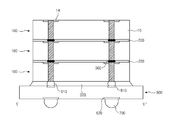
도 1 내지 도 3을 참조하면, 본 발명의 제1 실시예에 따른 반도체 칩(100)은, 기판(10), 다수개의 얼라인 범프(20)들 및 다수개의 얼리인 홈(30)들을 포함한다. 그 외에, 관통 전극(40)을 더 포함한다. 1 to 3, a
기판(10)은 제1 영역(First Region, FR) 및 제1 영역(FR) 바깥쪽에 배치되는 제2 영역(Second Region, SR)으로 구획되며, 일면(11), 타면(12), 측면(13), 회로부(미도시) 및 본딩 패드(14)를 포함한다. The
상기 일면(11)은 타면(12)과 대향하고, 측면(13)은 일면(11) 및 타면(12)을 연결한다.The one
회로부(미도시)는 기판(10)의 제1 영역(FR)에 형성되며 데이터를 저장, 처리 또는 전송하기 위한 트랜지스터, 커패시터 및 저항 등과 같은 소자를 포함한다. 본딩 패드(14)는 외부와의 연결을 위한 회로부의 전기적인 접점으로써, 제1 영역(FR)의 기판(10) 일면(11)에 형성된다. 비록, 본 실시예에서는 본딩 패드(14)가 제1 영역(FR)의 기판(10) 일면(11)에 형성된 경우만을 도시 및 설명하였으나, 이와 달리 본딩 패드(14)는 제1 영역(FR)의 기판(10) 타면(12)에 형성될 수도 있다. The circuit unit (not shown) is formed in the first region FR of the
얼라인 범프(20)들은 제2 영역(SR)의 기판(10) 일면(11)에 형성되며, 상이한 직경을 갖는 적어도 2개 이상의 범프들로 구성된다. 본 실시예에서, 얼라인 범프(20)들은 상이한 직경을 갖는 제1,제2,제3,제4 얼라인 범프(21,22,23,24)를 포함한다. 상기 제1,제2,제3,제4 얼라인 범프(21,22,23,24) 중에서 제1 얼라인 범프(21)의 직경이 가장 크고, 제1 얼라인 범프(21) 다음으로 제2 얼라인 범프(22)의 직경이 크고, 제2 얼라인 범프(22) 다음으로 제3 얼라인 범프(23)의 직경이 크고, 제4 얼라인 범프(24)의 직경이 가장 작다.The
본 실시예에서, 얼라인 범프(20)들은 그 직경의 크기에 비례하는 높이를 갖는다. 예컨데, 직경이 가장 큰 제1 얼라인 범프(21)의 높이가 가장 크고, 제1 얼라인 범프(21) 다음으로 제2 얼라인 범프(22)의 높이가 크고, 제2 얼라인 범프(22) 다음으로 제3 얼라인 범프(23)의 높이가 크며, 직경이 가장 작은 제4 얼라인 범프(24)의 높이가 가장 작다. In this embodiment, the alignment bumps 20 have a height proportional to the size of their diameter. For example, the height of the
얼라인 홈(30)들은 제2 영역(SR)의 기판(10) 타면(12)에 형성되며, 상이한 직경을 갖는 적어도 2개 이상의 홈들로 구성된다. 본 실시예에서, 얼라인 홈(30)들은 상이한 직경을 갖는 제1,제2,제3,제4 얼라인 홈(31,32,33,34)을 포함한다. The
각각의 얼라인 홈(30)들은 얼라인 범프(20)들과 개별적으로 마주하도록 배치되고, 마주하는 얼라인 범프(20)들과 동일한 직경을 갖는다. 구체적으로, 제1 얼라인 홈(31)은 제1 얼라인 범프(21)와 마주하도록 배치되고 제1 얼라인 범프(21)와 동일한 직경을 가지며, 제2 얼라인 홈(32)은 제2 얼라인 범프(22)와 마주하도록 배치되고 제2 얼라인 범프(22)와 동일한 직경을 갖는다. 그리고, 제3 얼라인 홈(33)은 제3 얼라인 범프(23)와 마주하도록 배치되고 제3 얼라인 범프(23)와 동일한 직경을 가지며, 제4 얼라인 홈(34)은 제4 얼라인 범프(24)와 마주하도록 배치되고 제4 얼라인 범프(24)와 동일한 직경을 갖는다. Each of the
한편, 얼라인 범프(20)들 및 얼라인 홈(30)들 중 최소 사이즈를 갖는 제4 얼라인 범프(24) 및 제4 얼라인 홈(34)은 후술되는 관통 전극(40)보다 작은 직경을 갖도록 형성하는 것이 바람직하다. Meanwhile, the
본 실시예에서, 얼라인 범프(20)들 및 얼라인 홈(30)들은 직경 크기 순서에 따라서 일렬로 배열된다. 이와 달리, 도시하지는 않았지만 얼라인 범프(20)들 및 얼라인 홈(30)들은 직경 크기와 관계없이 랜덤(random)하게 배열될 수도 있다. In this embodiment, the alignment bumps 20 and the
관통 전극(40)은 제1 영역(FR) 기판(10)의 일면(11) 및 타면(12)을 관통하고, 본딩 패드(14)와 전기적으로 연결된다. 본 실시예에서, 관통 전극(40)은 본딩 패드(14)를 관통한다. 이와 다르게, 관통 전극(40)은 본딩 패드(14)를 관통하지 않고 본딩 패드(14)와 전기적으로 연결된 회로부의 일부분을 관통할 수도 있다.The through
이하, 전술한 반도체 칩을 갖는 적층 반도체 패키지를 설명하면 다음과 같다.Hereinafter, a multilayer semiconductor package having the semiconductor chip described above will be described.
도 4는 본 발명의 제1 실시예에 따른 적층 반도체 패키지를 도시한 사시도이고, 도 5는 도 4의 Ⅲ-Ⅲ' 라인에 따른 단면도이고, 도 6은 도 4의 Ⅳ-Ⅳ' 라인에 따른 단면도이다.4 is a perspective view illustrating a multilayer semiconductor package according to a first exemplary embodiment of the present invention, FIG. 5 is a cross-sectional view taken along line III-III ′ of FIG. 4, and FIG. 6 is taken along line IV-IV ′ of FIG. 4. It is a cross section.
도 4 내지 도 6을 참조하면, 얼라인 범프(20)들, 얼라인 홈(30)들 및 관통 전극(40)을 갖는 복수개의 반도체 칩(100)들이 마련된 후, 하부 반도체 칩(100)의 얼라인 범프(20)들과 상부 반도체 칩(100)의 얼라인 홈(30)들이 상호 결합되고, 하부 반도체 칩(100)의 관통 전극(40)과 상부 반도체 칩(100)의 관통 전극(40)이 전기적으로 연결되도록 복수개의 반도체 칩(100)들이 적층된다. 4 to 6, after the plurality of
적층되는 반도체 칩(100)들 사이에는 접착 부재(200)가 형성되고, 반도체 칩(100)들의 관통 전극(40)들 사이에는 전도성 연결 부재(300)가 형성된다. 접착 부재(200)는 비전도성 페이스트(Non-Conductive Paste)를 포함할 수 있고, 전도성 연결 부재(300)는 솔더(solder)를 포함할 수 있다. An
상기 적층된 반도체 칩(100)들 중 최하부 반도체 칩(100)의 하부면에는 관통 전극(40)을 노출하는 제1 절연층(400)이 형성되고, 제1 절연층(400) 상에는 최하부 반도체 칩(100)의 관통 전극(40)과 전기적으로 연결되는 재배선(500)이 형성된다. 그리고, 재배선(500)을 포함한 제1 절연층(400) 상에는 재배선(500)의 일부를 노출시키는 제2 절연층(600)이 형성되고, 제2 절연층(600)에 의해 노출된 재배선(500) 상에는 외부접속단자(700)가 장착된다. A first insulating
도 7은 본 발명의 제2 실시예에 따른 적층 반도체 패키지를 도시한 사시도이고, 도 8은 도 7의 Ⅴ-Ⅴ' 라인에 따른 단면도이다. FIG. 7 is a perspective view illustrating a multilayer semiconductor package according to a second exemplary embodiment of the present invention, and FIG. 8 is a cross-sectional view taken along the line VV ′ of FIG. 7.
도 7 및 도 8을 참조하면, 얼라인 범프(20)들, 얼라인 홈(30)들 및 관통 전극(40)을 갖는 복수개의 반도체 칩(100)들이 마련된 후, 하부 반도체 칩(100)의 얼라인 범프(20)들과 상부 반도체 칩(100)의 얼라인 홈(30)들이 상호 결합되고, 하부 반도체 칩(100)의 관통 전극(40)과 상부 반도체 칩(100)의 관통 전극(40)이 전기적으로 연결되도록 복수개의 반도체 칩(100)들이 적층된다. 7 and 8, after a plurality of
적층되는 반도체 칩(100)들 사이에는 접착 부재(200)가 형성되고, 반도체 칩(100)들의 관통 전극(40)들 사이에는 전도성 연결 부재(300)가 형성된다. 접착 부재(200)는 비전도성 페이스트를 포함할 수 있고, 전도성 연결 부재(300)는 솔더(solder)를 포함할 수 있다. An
적층된 반도체 칩(100)들은, 최하부 반도체 칩(100)의 관통 전극(40)이 구조체(800)의 접속 전극(810)과 전기적으로 연결되도록, 구조체(800) 상에 실장된다.본 실시예에서, 구조체(800)는 인쇄회로기판(Printed Circuit Board, PCB)으로 형성된다.The stacked
최하부 반도체 칩(100)의 관통 전극(40)과 구조체(800)의 접속 전극(810)은 전도성 연결 부재(910)에 의하여 전기적으로 연결된다. 그리고, 최하부 반도체 칩(100)과 구조체(800) 사이에는 접착 부재(920)이 형성된다. 미설명된 도면부호 820은 볼랜드를, 700은 볼랜드(820)에 장착되는 외부접속단자를 나타낸다.The through
비록, 본 실시예에서는 구조체(800)가 인쇄회로기판인 경우만을 도시 및 설명하였으나, 구조체(800)는 반도체 패키지, 인터포저 등 다른 반도체 구조물일 수도 있다.Although the
도 9는 본 발명의 제3 실시예에 따른 적층 반도체 패키지를 도시한 단면도이다.9 is a cross-sectional view illustrating a multilayer semiconductor package according to a third exemplary embodiment of the present invention.
본 발명의 제3 실시예에 따른 적층 반도체 패키지는, 앞서 도 4 내지 도 6을 통해 설명된 제1 실시예에 따른 적층 반도체 패키지에 추가 반도체 칩(100A)이 추가된 구성을 갖는다. 따라서, 추가 반도체 칩(100A)을 제외하면 제1 실시예에 따른 적층 반도체 패키지와 실질적으로 동일한 구성을 갖는다. 따라서, 동일한 구성요소에 대한 중복된 설명은 생략하기로 하며, 동일한 구성요소에 대해서는 동일한 명칭 및 동일한 참조 부호를 부여하기로 한다.The multilayer semiconductor package according to the third embodiment of the present invention has a configuration in which an
도 9를 참조하면, 얼라인 범프(20)들, 얼라인 홈(30)들 및 관통 전극(40)을 갖는 복수개의 반도체 칩(100)들이 마련된 후, 하부 반도체 칩(100)의 얼라인 범프(20)들과 상부 반도체 칩(100)의 얼라인 홈(30)들이 상호 결합되고, 하부 반도체 칩(100)의 관통 전극(40)과 상부 반도체 칩(100)의 관통 전극(40)이 전기적으로 연결되도록 복수개의 반도체 칩(100)들이 적층된다. Referring to FIG. 9, after the plurality of
그리고, 적층된 반도체 칩(100)들 중 최상부 반도체 칩(100) 상에 최상부 반도체 칩(100)의 얼라인 범프(20)들과 결합되는 얼라인 홈(30A)들을 갖는 추가 반도체 칩(100A)이 적층된다. Further, the
도시하지 않았지만, 추가 반도체 칩(100A)은 최상부 반도체 칩(100)의 관통 전극(40)과 전기적으로 연결되는 본딩 패드를 구비한다. 그 외에, 추가 반도체 칩(100A)은 최상부 반도체 칩(100)의 관통 전극(40)과 전기적으로 연결되는 관통 전극을 더 구비할 수도 있다. Although not shown, the
그리고, 적층되는 반도체 칩(100)들 및 추가 반도체 칩(100A)들 사이에는 접착 부재(200)가 형성되고, 반도체 칩(100)들의 관통 전극(40)들 사이에는 전도성 연결 부재(300)가 형성된다. 접착 부재(200)는 비전도성 페이스트를 포함할 수 있고, 전도성 연결 부재(300)는 솔더를 포함할 수 있다. In addition, an
도 10은 본 발명의 제4 실시예에 따른 적층 반도체 패키지를 도시한 단면도이다.10 is a cross-sectional view showing a laminated semiconductor package according to a fourth embodiment of the present invention.
본 발명의 제4 실시예에 따른 적층 반도체 패키지는, 앞서 도 4 내지 도 6을 통해 설명된 제1 실시예에 따른 적층 반도체 패키지에 추가 반도체 칩(100B)이 추가된 구성을 갖는다. 따라서, 추가 반도체 칩(100B)을 제외하면 제1 실시예에 따른 적층 반도체 패키지와 실질적으로 동일한 구성을 갖는다. 따라서, 동일한 구성요소에 대한 중복된 설명은 생략하기로 하며, 동일한 구성요소에 대해서는 동일한 명칭 및 동일한 참조 부호를 부여하기로 한다.The multilayer semiconductor package according to the fourth embodiment of the present invention has a configuration in which an
도 10을 참조하면, 얼라인 범프(20)들, 얼라인 홈(30)들 및 관통 전극(40)을 갖는 복수개의 반도체 칩(100)들이 마련된 후, 하부 반도체 칩(100)의 얼라인 범프(20)들과 상부 반도체 칩(100)의 얼라인 홈(30)들이 상호 결합되고, 하부 반도체 칩(100)의 관통 전극(40)과 상부 반도체 칩(100)의 관통 전극(40)이 전기적으로 연결되도록 복수개의 반도체 칩(100)들이 적층된다. Referring to FIG. 10, after the plurality of
적층된 반도체 칩(100)들 중 최하부 반도체 칩(100) 상에 최하부 반도체 칩(100)의 얼라인 홈(30)들과 결합되는 얼라인 범프(20B)들을 갖는 추가 반도체 칩(100B)이 적층된다. 도시하지 않았지만, 추가 반도체 칩(100B)은 최하부 반도체 칩(100)의 관통 전극(40)과 전기적으로 연결되는 관통 전극(미도시)을 구비한다. The
그리고, 적층되는 반도체 칩(100)들 및 추가 반도체 칩(100B)들 사이에는 접착 부재(200)가 형성되고, 반도체 칩(100)들의 관통 전극(40)들 사이에는 전도성 연결 부재(300)가 형성된다. 접착 부재(200)는 비전도성 페이스트를 포함할 수 있고, 전도성 연결 부재(300)는 솔더를 포함할 수 있다. The
상기 추가 반도체 칩(100B)의 하부면에는 추가 반도체 칩(100B)의 관통 전극을 노출하는 제1 절연층(400)이 형성되고, 제1 절연층(400) 상에는 추가 반도체 칩(100B)의 관통 전극과 전기적으로 연결되는 재배선(500)이 형성된다. 그리고, 재배선(500)을 포함한 제1 절연층(400) 상에는 재배선(500)의 일부를 노출시키는 제2 절연층(600)이 형성되고, 제2 절연층(600)에 의해 노출된 재배선(500) 상에는 외부접속단자(700)가 장착된다. The first insulating
도 11은 본 발명의 제5 실시예에 따른 적층 반도체 패키지를 도시한 단면도이다.11 is a cross-sectional view illustrating a multilayer semiconductor package according to a fifth exemplary embodiment of the present invention.
본 발명의 제5 실시예에 따른 적층 반도체 패키지는, 앞서 도 4 내지 도 6을 통해 설명된 제1 실시예에 따른 적층 반도체 패키지에 제1 추가 반도체 칩(100A) 및 제2 추가 반도체 칩(100B)이 추가된 구성을 갖는다. 따라서, 제1,제2 추가 반도체 칩(100A, 100B)을 제외하면 제1 실시예에 따른 적층 반도체 패키지와 실질적으로 동일한 구성을 갖는다. 따라서, 동일한 구성요소에 대한 중복된 설명은 생략하기로 하며, 동일한 구성요소에 대해서는 동일한 명칭 및 동일한 참조 부호를 부여하기로 한다.In the multilayer semiconductor package according to the fifth embodiment of the present invention, the first
도 11을 참조하면, 얼라인 범프(20)들, 얼라인 홈(30)들 및 관통 전극(40)을 갖는 복수개의 반도체 칩(100)들이 마련된 후, 하부 반도체 칩(100)의 얼라인 범프(20)들과 상부 반도체 칩(100)의 얼라인 홈(30)들이 상호 결합되고, 하부 반도체 칩(100)의 관통 전극(40)과 상부 반도체 칩(100)의 관통 전극(40)이 전기적으로 연결되도록 복수개의 반도체 칩(100)들이 적층된다. Referring to FIG. 11, after the plurality of
그리고, 적층된 반도체 칩(100) 중 최상부 반도체 칩(100) 상에 최상부 반도체 칩(100)의 얼라인 범프(20)들과 결합되는 얼라인 홈(30A)들을 갖는 제1 추가 반도체 칩(100A)이 적층되고, 최하부 반도체 칩(100) 상에 최하부 반도체 칩(100)의 얼라인 홈(30)들과 결합되는 얼라인 범프(20B)들을 갖는 제2 추가 반도체 칩(100B)이 적층된다. In addition, the first
도시하지 않았지만, 제1 추가 반도체 칩(100A)은 최상부 반도체 칩(100)의 관통 전극(40)과 전기적으로 연결되는 본딩 패드를 구비한다. 그 외에, 제1 추가 반도체 칩(100A)은 최상부 반도체 칩(100)의 관통 전극(40)과 전기적으로 연결되는 관통 전극을 더 구비할 수도 있다. 그리고, 제2 추가 반도체 칩(100B)은 최하부 반도체 칩(100)의 관통 전극(40)과 전기적으로 연결되는 관통 전극을 구비한다. Although not illustrated, the first
그리고, 적층되는 반도체 칩(100)들 및 제1, 제2 추가 반도체 칩(100A, 100B) 사이에는 접착 부재(200)가 형성되고, 반도체 칩(100)들의 관통 전극(40)들 및 제1, 제2 추가 반도체 칩(100A,100B)의 관통 전극들 사이에는 전도성 연결 부재(300)가 형성된다. 접착 부재(200)는 비전도성 페이스트를 포함할 수 있고, 전도성 연결 부재(300)는 솔더를 포함할 수 있다. The
상기 제2 추가 반도체 칩(100B)의 하부면에는 제2 추가 반도체 칩(100B)의 관통 전극을 노출하는 제1 절연층(400)이 형성되고, 제1 절연층(400) 상에는 제2 추가 반도체 칩(100B)의 관통 전극과 전기적으로 연결되는 재배선(500)이 형성된다. 그리고, 재배선(500)을 포함한 제1 절연층(400) 상에는 재배선(500)의 일부를 노출시키는 제2 절연층(600)이 형성되고, 제2 절연층(600)에 의해 노출된 재배선(500) 상에는 외부접속단자(700)가 장착된다. A first insulating
도 12는 본 발명에 따른 적층 반도체 패키지를 구비한 전자 장치를 도시한 사시도이다. 12 is a perspective view illustrating an electronic device having a stacked semiconductor package according to the present invention.
도 12를 참조하면, 본 발명의 실시예에 따른 적층 반도체 패키지는 휴대폰과 같은 전자 장치(1000)에 응용될 수 있다. 본 실시예의 적층 반도체 패키지는 불량 개선의 장점을 가지므로, 전자 장치(1000)의 신뢰성 향상에 유리하다. 전자 장치는 도 12에 도시된 휴대폰에 한정되는 것이 아니며, 가령 모바일 전자 기기, 랩톱(laptop) 컴퓨터, 휴대용 컴퓨터, 포터블 멀티미디어 플레이어(PMP), 엠피쓰리(MP3) 플레이어, 캠코더, 웹 태블릿(web tablet), 무선 전화기, 네비게이션, 개인 휴대용 정보 단말기(PDA; Personal Digital Assistant) 등 다양한 전자 기기를 포함할 수 있다.Referring to FIG. 12, the multilayer semiconductor package according to an embodiment of the present invention may be applied to an
도 13은 본 발명에 따른 적층 반도체 패키지를 포함하는 전자 장치의 예를 보여주는 블럭도이다. 13 is a block diagram illustrating an example of an electronic device including a stacked semiconductor package according to the present disclosure.
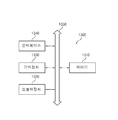
도 13을 참조하면, 전자 시스템(1300)은 제어기(1310), 입출력 장치(1320) 및 기억 장치(1330)를 포함할 수 있다. 상기 제어기(1310), 입출력 장치(1320) 및 기억 장치(1330)는 버스(1350, bus)를 통하여 결합될 수 있다. 상기 버스(1350)는 데이터들이 이동하는 통로라 할 수 있다. 예컨대, 상기 제어기(1310)는 적어도 하나의 마이크로프로세서, 디지털 신호 프로세서, 마이크로컨트롤러, 그리고 이들과 동일한 기능을 수행할 수 있는 논리 소자들 중에서 적어도 어느 하나를 포함할 수 있다. 상기 제어기(1310) 및 기억 장치(1330)는 본 발명에 따른 적층 반도체 패키지를 포함할 수 있다. 상기 입출력 장치(1320)는 키패드, 키보드 및 표시 장치(display device) 등에서 선택된 적어도 하나를 포함할 수 있다. 상기 기억 장치(1330)는 데이터를 저장하는 장치이다. 상기 기억 장치(1330)는 데이터 및/또는 상기 제어기(1310)에 의해 실행되는 명령어 등을 저장할 수 있다. 상기 기억 장치(1330)는 휘발성 기억 소자 및/또는 비휘발성 기억 소자를 포함할 수 있다. 또는, 상기 기억 장치(1330)는 플래시 메모리로 형성될 수 있다. 예를 들면, 모바일 기기나 데스크 톱 컴퓨터와 같은 정보 처리 시스템에 본 발명의 기술이 적용된 플래시 메모리가 장착될 수 있다. 이러한 플래시 메모리는 SSD(Solide State Drive)로 구성될 수 있다. 이 경우 전자 시스템(1300)은 대용량의 데이터를 상기 플래시 메모리 시스템에 안정적으로 저장할 수 있다. 상기 전자 시스템(1300)은 통신 네트워크로 데이터를 전송하거나 통신 네트워크로부터 데이터를 수신하기 위한 인터페이스(1340)를 더 포함할 수 있다. 상기 인터페이스(1340)는 유무선 형태일 수 있다. 예컨대, 상기 인터페이스(1340)는 안테나 또는 유무선 트랜시버 등을 포함할 수 있다. 그리고, 도시되지 않았지만, 상기 전자 시스템(1300)에는 응용 칩셋(Application Chipset), 카메라 이미지 프로세서(Camera Image Processor:CIP), 그리고 입출력 장치 등이 더 제공될 수 있음은 이 분야의 통상적인 지식을 습득한 자들에게 자명하다.Referring to FIG. 13, the
본 발명에 따르면, 반도체 칩 적층시 향상된 얼라인 정확도가 향상되므로 적층되는 반도체 칩들간 미스 얼라인으로 인한 접속 불량이 방지되어 수율이 향상된다. 또한, 적층되는 반도체 칩들간 결속력이 향상되어 외부 충격이나 열팽창 계수 차이로 인한 변형이 감소되므로 제품의 신뢰성이 향상된다. According to the present invention, improved alignment accuracy is improved when stacking semiconductor chips, thereby preventing poor connection due to misalignment between stacked semiconductor chips, thereby improving yield. In addition, since the binding force between the stacked semiconductor chips is improved, deformation due to external shock or thermal expansion coefficient difference is reduced, thereby improving product reliability.
앞서 설명한 본 발명의 상세한 설명에서는 본 발명의 실시예들을 참조하여 설명하였지만, 해당 기술분야의 숙련된 당업자 또는 해당 기술분야에 통상의 지식을 갖는 자라면 후술 될 특허청구범위에 기재된 본 발명의 사상 및 기술 영역으로부터 벗어나지 않는 범위 내에서 본 발명을 다양하게 수정 및 변경시킬 수 있음을 이해할 수 있을 것이다.While the present invention has been described in connection with what is presently considered to be the most practical and preferred embodiment, it is to be understood that the invention is not limited to the disclosed embodiments, but, on the contrary, It will be understood that the invention can be variously modified and changed without departing from the technical scope thereof.
100 : 반도체 칩
10 : 기판
20 : 얼라인 범프들
30 : 얼라인 홈들
40 : 관통 전극100: semiconductor chip
10: substrate
20: alignment bumps
30: alignment grooves
40: through electrode
Claims (20)
상기 기판의 일면에 형성되며 상이한 직경을 갖는 적어도 2개 이상의 얼라인 범프들;
상기 기판의 타면에 형성되며 상이한 직경을 갖는 적어도 2개 이상의 얼라인 홈들을 포함하는 반도체 칩.A substrate having one surface and the other surface opposite to the one surface;
At least two alignment bumps formed on one surface of the substrate and having different diameters;
And at least two alignment grooves formed on the other surface of the substrate and having different diameters.
상기 본딩 패드와 전기적으로 연결되며 데이터를 저장, 처리 또는 전송하기 위한 회로부를 더 포함하는 것을 특징으로 하는 반도체 칩.The method of claim 1, wherein the substrate comprises: a bonding pad formed on one surface of the substrate; And
And a circuit unit electrically connected to the bonding pad and configured to store, process, or transmit data.
상기 얼라인 범프들은 상기 기판 일면의 상기 제2 영역에 배치되고, 상기 얼라인 홈들은 상기 기판 타면의 상기 제2 영역에 배치되는 것을 특징으로 하는 반도체 칩.The method of claim 7, wherein the substrate is divided into a first region in which the bonding pad and the circuit unit are located, and a second region disposed outside the first region.
And the alignment bumps are disposed in the second region of one surface of the substrate, and the alignment grooves are disposed in the second region of the other surface of the substrate.
상기 반도체 칩들 사이에 형성되는 접착 부재를 포함하며,
상기 반도체 칩들은 하부 반도체 칩의 얼라인 범프들과 상부 반도체 칩의 얼라인 홈들간 결합에 의해 얼라인되는 것을 특징으로 하는 적층 반도체 패키지.A substrate having one surface and the other surface opposite to the one surface, at least two alignment bumps formed on one surface of the substrate and having different diameters, and at least two different shapes formed on the other surface of the substrate and having different diameters A plurality of semiconductor chips each having phosphorus grooves and stacked;
An adhesive member formed between the semiconductor chips,
And the semiconductor chips are aligned by coupling between alignment bumps of the lower semiconductor chip and the alignment grooves of the upper semiconductor chip.
상기 본딩 패드와 전기적으로 연결되며 데이터를 저장, 처리 또는 전송하는 회로부를 더 포함하는 것을 특징으로 하는 적층 반도체 패키지.The semiconductor device of claim 11, wherein the substrate of each semiconductor chip comprises: a bonding pad formed on one surface of the substrate; And
And a circuit unit electrically connected to the bonding pad and configured to store, process, or transmit data.
상기 얼라인 홈들은 상기 기판 일면의 상기 제2 영역에 배치되고, 상기 얼라인 범프들은 상기 기판 타면의 상기 제2 영역에 배치되는 것을 특징으로 하는 적층 반도체 패키지.The semiconductor device of claim 16, wherein the substrate of each of the semiconductor chips is divided into a first region in which the circuit portion is located and a second region disposed outside the first region.
And the alignment grooves are disposed in the second region of one surface of the substrate, and the alignment bumps are disposed in the second region of the other surface of the substrate.
Priority Applications (2)
| Application Number | Priority Date | Filing Date | Title |
|---|---|---|---|
| KR1020120047062A KR20130123722A (en) | 2012-05-03 | 2012-05-03 | Semiconductor chip and stacked semiconductor package having the same |
| US13/614,222 US8884445B2 (en) | 2012-05-03 | 2012-09-13 | Semiconductor chip and stacked semiconductor package having the same |
Applications Claiming Priority (1)
| Application Number | Priority Date | Filing Date | Title |
|---|---|---|---|
| KR1020120047062A KR20130123722A (en) | 2012-05-03 | 2012-05-03 | Semiconductor chip and stacked semiconductor package having the same |
Publications (1)
| Publication Number | Publication Date |
|---|---|
| KR20130123722A true KR20130123722A (en) | 2013-11-13 |
Family
ID=49511917
Family Applications (1)
| Application Number | Title | Priority Date | Filing Date |
|---|---|---|---|
| KR1020120047062A Withdrawn KR20130123722A (en) | 2012-05-03 | 2012-05-03 | Semiconductor chip and stacked semiconductor package having the same |
Country Status (2)
| Country | Link |
|---|---|
| US (1) | US8884445B2 (en) |
| KR (1) | KR20130123722A (en) |
Cited By (1)
| Publication number | Priority date | Publication date | Assignee | Title |
|---|---|---|---|---|
| US11637075B2 (en) | 2020-09-02 | 2023-04-25 | SK Hynix Inc. | Semiconductor device having three-dimensional structure |
Families Citing this family (8)
| Publication number | Priority date | Publication date | Assignee | Title |
|---|---|---|---|---|
| JP2015005637A (en) | 2013-06-21 | 2015-01-08 | ピーエスフォー ルクスコ エスエイアールエルPS4 Luxco S.a.r.l. | Semiconductor device |
| KR102427557B1 (en) | 2017-09-29 | 2022-08-01 | 삼성전자주식회사 | Semiconductor package |
| KR102722915B1 (en) | 2019-10-30 | 2024-10-28 | 삼성전자주식회사 | Semiconductor package and method for fabricating the same |
| US12159850B2 (en) | 2020-12-25 | 2024-12-03 | Yibu Semiconductor Co., Ltd. | Semiconductor packaging method, semiconductor assembly and electronic device comprising semiconductor assembly |
| US12154884B2 (en) | 2021-02-01 | 2024-11-26 | Yibu Semiconductor Co., Ltd. | Semiconductor packaging method, semiconductor assembly and electronic device comprising semiconductor assembly |
| US12500203B2 (en) | 2021-02-22 | 2025-12-16 | Yibu Semiconductor Co., Ltd. | Semiconductor packaging method, semiconductor assembly and electronic device comprising semiconductor assembly |
| CN113078147B (en) * | 2021-02-22 | 2023-08-15 | 上海易卜半导体有限公司 | Semiconductor packaging method, semiconductor assembly and electronic device comprising semiconductor assembly |
| KR20230056188A (en) * | 2021-10-20 | 2023-04-27 | 삼성전자주식회사 | Semiconductor package |
Family Cites Families (3)
| Publication number | Priority date | Publication date | Assignee | Title |
|---|---|---|---|---|
| US6778404B1 (en) * | 2000-06-02 | 2004-08-17 | Micron Technology Inc | Stackable ball grid array |
| KR20090047776A (en) * | 2007-11-08 | 2009-05-13 | 삼성전자주식회사 | Semiconductor element and method of forming the same |
| KR20120048841A (en) | 2010-11-08 | 2012-05-16 | 에스케이하이닉스 주식회사 | Stacked semiconductor package |
-
2012
- 2012-05-03 KR KR1020120047062A patent/KR20130123722A/en not_active Withdrawn
- 2012-09-13 US US13/614,222 patent/US8884445B2/en not_active Expired - Fee Related
Cited By (1)
| Publication number | Priority date | Publication date | Assignee | Title |
|---|---|---|---|---|
| US11637075B2 (en) | 2020-09-02 | 2023-04-25 | SK Hynix Inc. | Semiconductor device having three-dimensional structure |
Also Published As
| Publication number | Publication date |
|---|---|
| US8884445B2 (en) | 2014-11-11 |
| US20130292843A1 (en) | 2013-11-07 |
Similar Documents
| Publication | Publication Date | Title |
|---|---|---|
| KR20130123722A (en) | Semiconductor chip and stacked semiconductor package having the same | |
| CN103258806B (en) | Semiconductor package structure with bridge structure and manufacturing method thereof | |
| CN111490029A (en) | Semiconductor package including bridge die | |
| KR102110405B1 (en) | semiconductor package and manufacturing method of the same | |
| KR20110045222A (en) | Semiconductor package and manufacturing method thereof | |
| US9780071B2 (en) | Stacked semiconductor package including reconfigurable package units | |
| CN112397486A (en) | Semiconductor package including stacked semiconductor chips | |
| KR101904926B1 (en) | Semiconductor package | |
| US20170062384A1 (en) | Semiconductor package embedded with plurality of chips and method of manufacturing the same | |
| CN104779218B (en) | Chip package structure | |
| US20160163608A1 (en) | Semiconductor package | |
| US9087819B2 (en) | Semiconductor package and stack-type semiconductor package having the same | |
| US8803325B2 (en) | Stacked semiconductor package | |
| US20170200688A1 (en) | Semiconductor package having a bump bonding structure | |
| US9082686B2 (en) | Semiconductor package | |
| US9515054B2 (en) | Semiconductor device and stacked semiconductor package having the same | |
| JP2012138401A (en) | Semiconductor device manufacturing method | |
| KR20140023070A (en) | Conductive bump, semiconductor chip and stacked semiconductor package using the same | |
| CN102386180A (en) | Semiconductor integrated circuit | |
| US20130292818A1 (en) | Semiconductor chip, semiconductor package having the same, and stacked semiconductor package using the semiconductor package | |
| US20170084575A1 (en) | Semiconductor package embedded with a plurality of chips | |
| KR20130104728A (en) | Semiconductor chip and stacked semiconductor package having the same | |
| US20160086912A1 (en) | Methods for semiconductor package | |
| US20140015126A1 (en) | Semiconductor package and stacked semiconductor package using the same | |
| KR102188644B1 (en) | Semiconductor package having extanded bandwidth |
Legal Events
| Date | Code | Title | Description |
|---|---|---|---|
| PA0109 | Patent application |
St.27 status event code: A-0-1-A10-A12-nap-PA0109 |
|
| PN2301 | Change of applicant |
St.27 status event code: A-3-3-R10-R13-asn-PN2301 St.27 status event code: A-3-3-R10-R11-asn-PN2301 |
|
| PG1501 | Laying open of application |
St.27 status event code: A-1-1-Q10-Q12-nap-PG1501 |
|
| PN2301 | Change of applicant |
St.27 status event code: A-3-3-R10-R13-asn-PN2301 St.27 status event code: A-3-3-R10-R11-asn-PN2301 |
|
| PC1203 | Withdrawal of no request for examination |
St.27 status event code: N-1-6-B10-B12-nap-PC1203 |
|
| WITN | Application deemed withdrawn, e.g. because no request for examination was filed or no examination fee was paid | ||
| P22-X000 | Classification modified |
St.27 status event code: A-2-2-P10-P22-nap-X000 |