KR20130111031A - Semiconductor light emitting device - Google Patents
Semiconductor light emitting device Download PDFInfo
- Publication number
- KR20130111031A KR20130111031A KR1020120033491A KR20120033491A KR20130111031A KR 20130111031 A KR20130111031 A KR 20130111031A KR 1020120033491 A KR1020120033491 A KR 1020120033491A KR 20120033491 A KR20120033491 A KR 20120033491A KR 20130111031 A KR20130111031 A KR 20130111031A
- Authority
- KR
- South Korea
- Prior art keywords
- layer
- light emitting
- emitting device
- semiconductor layer
- type semiconductor
- Prior art date
- Legal status (The legal status is an assumption and is not a legal conclusion. Google has not performed a legal analysis and makes no representation as to the accuracy of the status listed.)
- Withdrawn
Links
Images


Classifications
-
- H—ELECTRICITY
- H10—SEMICONDUCTOR DEVICES; ELECTRIC SOLID-STATE DEVICES NOT OTHERWISE PROVIDED FOR
- H10H—INORGANIC LIGHT-EMITTING SEMICONDUCTOR DEVICES HAVING POTENTIAL BARRIERS
- H10H20/00—Individual inorganic light-emitting semiconductor devices having potential barriers, e.g. light-emitting diodes [LED]
- H10H20/80—Constructional details
- H10H20/83—Electrodes
- H10H20/832—Electrodes characterised by their material
- H10H20/833—Transparent materials
-
- H—ELECTRICITY
- H10—SEMICONDUCTOR DEVICES; ELECTRIC SOLID-STATE DEVICES NOT OTHERWISE PROVIDED FOR
- H10H—INORGANIC LIGHT-EMITTING SEMICONDUCTOR DEVICES HAVING POTENTIAL BARRIERS
- H10H20/00—Individual inorganic light-emitting semiconductor devices having potential barriers, e.g. light-emitting diodes [LED]
- H10H20/80—Constructional details
- H10H20/83—Electrodes
- H10H20/831—Electrodes characterised by their shape
- H10H20/8312—Electrodes characterised by their shape extending at least partially through the bodies
-
- H—ELECTRICITY
- H10—SEMICONDUCTOR DEVICES; ELECTRIC SOLID-STATE DEVICES NOT OTHERWISE PROVIDED FOR
- H10H—INORGANIC LIGHT-EMITTING SEMICONDUCTOR DEVICES HAVING POTENTIAL BARRIERS
- H10H20/00—Individual inorganic light-emitting semiconductor devices having potential barriers, e.g. light-emitting diodes [LED]
- H10H20/80—Constructional details
- H10H20/83—Electrodes
- H10H20/832—Electrodes characterised by their material
- H10H20/835—Reflective materials
Landscapes
- Led Devices (AREA)
Abstract
본 발명의 실시형태에 따른 반도체 발광 소자는, n형 반도체층; 상기 n형 반도체층과 서로 마주보게 형성된 p형 반도체층; 상기 n형 반도체층과 p형 반도체층 사이에 형성된 활성층; 및 상기 n형 반도체층 및 p형 반도체층 중 적어도 하나를 덮도록 형성되며, 그래핀층과 상기 그래핀층을 관통하는 접촉층으로 이루어진 전극;을 구비한다.A semiconductor light emitting device according to an embodiment of the present invention, an n-type semiconductor layer; A p-type semiconductor layer formed to face the n-type semiconductor layer; An active layer formed between the n-type semiconductor layer and the p-type semiconductor layer; And an electrode formed to cover at least one of the n-type semiconductor layer and the p-type semiconductor layer, the electrode including a graphene layer and a contact layer penetrating through the graphene layer.
Description
본 발명은 반도체 발광 소자에 관한 것이다.
The present invention relates to a semiconductor light emitting device.
발광 소자(Light Emitting Device; LED)는 화합물 반도체의 P-N 접합 구조를 이용하여 소수 캐리어(전자 또는 정공)를 만들고, 이들의 재결합에 의하여 소정의 빛을 발산하는 소자이다. 발광 소자는 GaAs, AlGaAs, GaN, InGaN, AlGaInP 등의 화합물 반도체(compound semiconductor) 재료를 변경하여 발광원을 구성함으로써 다양한 색을 구현할 수 있다. 발광 소자는 기존의 전구 또는 형광등에 비해 소모 전력이 작고 수명이 길기 때문에 최근 일반 조명은 물론 액정 표시 장치의 백라이트, 자동차 헤드라이트까지 응용이 확대되고 있다.A light emitting device (LED) is a device that makes a minority carrier (electron or hole) by using a P-N junction structure of a compound semiconductor and emits predetermined light by recombination thereof. The light emitting device can realize various colors by changing a compound semiconductor material such as GaAs, AlGaAs, GaN, InGaN, AlGaInP, and the like to form a light emitting source. Since the light emitting device consumes less power and has a longer lifespan than conventional light bulbs or fluorescent lamps, applications have recently been extended to general lighting, backlights of liquid crystal display devices, and automobile headlights.
이러한 발광 소자에서 투명 전극으로 투명도전성 박막이 사용되는데, 우수한 광 투과성 및 도전성이 요구된다.In such a light emitting device, a transparent conductive thin film is used as the transparent electrode, and excellent light transmittance and conductivity are required.
현재 고품위의 투명도전성 박막으로 가장 많이 사용되고 있는 재료는 ITO이다. 그러나, ITO는 최근 가격이 급등하여 매우 고가이고, 전기전도도가 낮은 문제점이 있으며, 특히 단파장 영역에서 광 투과성이 매우 낮아지게 되는 문제점이 있다.
Currently, ITO is the most widely used high quality transparent conductive thin film. However, ITO is very expensive due to the recent surge in price, has a problem of low electrical conductivity, and particularly has a problem that the light transmittance is very low in the short wavelength region.
따라서 단파장 영역에서 광 투과성이 높고, 보다 전기적 특성이 향상된 투명 전극을 포함하는 반도체 발광 소자가 요구되고 있다.
Accordingly, there is a need for a semiconductor light emitting device including a transparent electrode having high light transmittance and improved electrical characteristics in a short wavelength region.
본 발명의 일 실시형태에 따른 반도체 발광 소자는, n형 반도체층; 상기 n형 반도체층과 서로 마주보게 형성된 p형 반도체층; 상기 n형 반도체층과 p형 반도체층 사이에 형성된 활성층; 및 상기 n형 반도체층 및 p형 반도체층 중 적어도 하나를 덮도록 형성되며, 그래핀층과 상기 그래핀층을 관통하는 접촉층으로 이루어진 전극;을 구비한다.A semiconductor light emitting device according to an embodiment of the present invention, an n-type semiconductor layer; A p-type semiconductor layer formed to face the n-type semiconductor layer; An active layer formed between the n-type semiconductor layer and the p-type semiconductor layer; And an electrode formed to cover at least one of the n-type semiconductor layer and the p-type semiconductor layer, the electrode including a graphene layer and a contact layer penetrating through the graphene layer.
상기 접촉층은 금속, 합금 및 산화물로 이루어진 군에서 선택된 어느 하나의 물질로 이루어진 것을 특징으로 한다.The contact layer is made of any one material selected from the group consisting of metals, alloys and oxides.
상기 접촉층은 은(Ag) 또는 니켈-은(Ni-Ag)합금으로 이루어진 것을 특징으로 한다.The contact layer is characterized in that made of silver (Ag) or nickel-silver (Ni-Ag) alloy.
상기 접촉층은 상기 그래핀층과 동일한 높이로 형성된 것을 특징으로 한다.The contact layer is characterized in that formed at the same height as the graphene layer.
상기 접촉층은 원기둥, 삼각기둥, 사각기둥 및 육각기둥으로 이루어진 군에서 선택된 어느 하나의 상을 갖는 것을 특징으로 한다.The contact layer is characterized in that it has any one phase selected from the group consisting of a cylinder, a triangular column, a square column and a hexagonal column.
상기 접촉층은 복수개로 이루어져 라인 패턴으로 배열된 것을 특징으로 한다.The contact layer is composed of a plurality, characterized in that arranged in a line pattern.
상기 접촉층은 격자 패턴으로 형성되는 것을 특징으로 한다.
The contact layer is characterized in that formed in a grid pattern.
본 발명의 일 실시형태에 따른 반도체 발광 소자는, n형 반도체층; 상기 n형 반도체층과 서로 마주보게 형성된 p형 반도체층; 상기 n형 반도체층과 p형 반도체층 사이에 형성된 활성층; 및 상기 n형 반도체층 및 p형 반도체층 중 적어도 하나를 덮도록 형성되며, 그래핀층과 접촉층으로 이루어지고, 상기 그래핀층은 상기 접촉층의 상부를 덮도록 형성된 전극; 을 구비한다.A semiconductor light emitting device according to an embodiment of the present invention, an n-type semiconductor layer; A p-type semiconductor layer formed to face the n-type semiconductor layer; An active layer formed between the n-type semiconductor layer and the p-type semiconductor layer; And an electrode formed to cover at least one of the n-type semiconductor layer and the p-type semiconductor layer, the graphene layer and a contact layer, and the graphene layer formed to cover an upper portion of the contact layer. Respectively.
상기 접촉층은 금속, 합금 및 산화물로 이루어진 군에서 선택된 어느 하나의 물질로 이루어진 것을 특징으로 한다.The contact layer is made of any one material selected from the group consisting of metals, alloys and oxides.
상기 접촉층은 은(Ag) 또는 니켈-은(Ni-Ag)합금으로 이루어진 것을 특징으로 한다.The contact layer is characterized in that made of silver (Ag) or nickel-silver (Ni-Ag) alloy.
상기 접촉층은 원기둥, 삼각기둥, 사각기둥 및 육각기둥으로 이루어진 군에서 선택된 어느 하나의 상을 갖는 것을 특징으로 한다.The contact layer is characterized in that it has any one phase selected from the group consisting of a cylinder, a triangular column, a square column and a hexagonal column.
상기 접촉층은 복수개로 이루어져 라인 패턴으로 배열된 것을 특징으로 한다.The contact layer is composed of a plurality, characterized in that arranged in a line pattern.
상기 접촉층은 격자 패턴으로 형성되는 것을 특징으로 한다.
The contact layer is characterized in that formed in a grid pattern.
본 발명은 그래핀을 사용하여 투명 전극을 형성하는 것을 그 특징으로 하고 있는데, 이와 같은 그래핀은 지구상에 많이 존재하는 흑연이 원료이므로 채취가 용이하고, ITO보다 더 투명하기 때문에 발광 효율이 향상되는 효과가 있다. 또한 그래핀은 높은 열전도도를 가지고 있기 때문에 발광 소자에서 발생하는 열의 분산에 유리하여 발광 소자의 온도를 낮추는 효과를 볼 수 있다. 이것은 반도체 발광 소자의 발광 효율을 더 좋게 하는 결과를 가져오며 발광 소자의 장수명화를 가능하게 한다. 그리고 그래핀은 전기 전도성이 매우 좋으므로, 전극 내의 우수한 전류 확산을 통하여 발광 효율이 향상되는 효과가 있다.The present invention is characterized in that to form a transparent electrode using a graphene, such graphene is easy to collect because the graphite is present on the earth a lot, because the luminous efficiency is improved because it is more transparent than ITO It works. In addition, since graphene has a high thermal conductivity, it is advantageous to dissipate heat generated in the light emitting device, thereby reducing the temperature of the light emitting device. This results in better light emission efficiency of the semiconductor light emitting device and enables long life of the light emitting device. And since graphene has a very good electrical conductivity, there is an effect that the luminous efficiency is improved through excellent current diffusion in the electrode.
이와 같은 그래핀을 사용한 투명 전극 내에 접촉층을 형성하여 투명 전극과 하부 반도체층과의 접촉성을 향상시켜 안정적인 투명 전극을 형성할 수 있는 효과가 있다.By forming a contact layer in the transparent electrode using the graphene as described above there is an effect that can improve the contact between the transparent electrode and the lower semiconductor layer to form a stable transparent electrode.
따라서 전기적 특성 및 광 투과성이 향상된 투명 전극을 포함하는 반도체 발광 소자를 형성할 수 있다.
Therefore, the semiconductor light emitting device including the transparent electrode having improved electrical characteristics and light transmittance can be formed.
도 1은 본 발명의 제1 실시형태에 따른 반도체 발광 소자의 단면도이다.
도 2는 본 발명의 제1 실시형태에 따른 투명 전극을 포함하는 반도체 발광 소자의 사시도이다.
도 3은 본 발명의 제2 실시형태에 따른 투명 전극을 포함하는 반도체 발광 소자의 사시도이다.
도 4는 본 발명의 제3 실시형태에 따른 투명 전극을 나타낸 사시도이다.
도 5는 본 발명의 제4 실시형태에 따른 발광 소자의 단면도이다.
도 6은 도 5에 도시된 투명 전극을 나타낸 사시도이다.
도 7은 본 발명의 제5 실시형태에 따른 투명 전극을 나타낸 사시도이다.1 is a cross-sectional view of a semiconductor light emitting device according to a first embodiment of the present invention.
2 is a perspective view of a semiconductor light emitting element including the transparent electrode according to the first embodiment of the present invention.
3 is a perspective view of a semiconductor light emitting element including a transparent electrode according to a second embodiment of the present invention.
4 is a perspective view showing a transparent electrode according to a third embodiment of the present invention.
5 is a cross-sectional view of a light emitting device according to a fourth embodiment of the present invention.
6 is a perspective view illustrating the transparent electrode illustrated in FIG. 5.
7 is a perspective view showing a transparent electrode according to a fifth embodiment of the present invention.
본 발명의 실시형태에 따른 반도체 발광 소자에 관한 사항을 도면을 참조하여 설명한다. 그러나, 본 발명의 실시형태는 여러 가지 다른 형태로 변형될 수 있으며, 본 발명의 범위가 이하 설명되는 실시예로 한정되는 것은 아니다. 본 발명의 실시형태는 본 발명이 속하는 기술분야에서 통상의 지식을 가진 자에게 본 발명을 보다 완전하게 설명하기 위하여 제공되는 것이다. The matters regarding the semiconductor light emitting element which concerns on embodiment of this invention are demonstrated with reference to drawings. However, embodiments of the present invention may be modified in various other forms, and the scope of the present invention is not limited to the examples described below. Embodiments of the present invention are provided to more completely explain the present invention to those skilled in the art.
따라서, 도면에 도시된 구성요소들의 형상 및 크기 등은 보다 명확한 설명을 위하여 과장될 수 있으며, 도면 상에서 실질적으로 동일한 구성과 기능을 가진 구성요소들은 동일한 참조부호를 사용할 것이다.
Therefore, the shape and size of the components shown in the drawings may be exaggerated for more clear description, components having substantially the same configuration and function in the drawings will use the same reference numerals.
본 발명에 따른 반도체 발광 소자는 투명 전극이 그래핀(graphene)을 포함하여 이루어진 것이 특징이다.The semiconductor light emitting device according to the present invention is characterized in that the transparent electrode comprises graphene (graphene).
그래핀은 탄소가 육각형의 형태로 서로 연결된 벌집 모양의 2차원 평면 구조를 이루는 물질이다. 그래핀은 얇고 투명하며, 화학적으로 안정성이 높은 탄소로 구성되어있어 전기 전도성이 뛰어나다. 반도체에 사용하는 실리콘보다 전기 전도성이 100배 이상 빠르고, 열 전도율도 뛰어나다.
Graphene is a honeycomb two-dimensional planar structure in which carbon is connected to each other in the form of a hexagon. Graphene is made of thin, transparent, chemically stable carbon, which has excellent electrical conductivity. It is 100 times faster in electrical conductivity than silicon used in semiconductors, and also has excellent thermal conductivity.
도 1을 참조하여 본 발명의 제1 실시형태에 따른 반도체 발광 소자에 대해 설명한다. A semiconductor light emitting device according to a first embodiment of the present invention will be described with reference to FIG. 1.
도 1을 참조하면, 본 발명의 일 실시형태에 따른 반도체 발광 소자(1)는 단파장 LED로서, 기판(110)과, 상기 기판(110) 상에 순차적으로 형성된 언도프 반도체층(120), n형 질화물 반도체층(130), 활성층(140) 및 p형 질화물 반도체층(150), 제1 투명 전극(160), n형 전극(170) 및 p형 전극(180)을 포함하여 구성된다.
Referring to FIG. 1, a semiconductor
상기 기판(110)은 질화물 반도체 발광소자를 제작하기 위한 웨이퍼를 지칭하는 것으로, 주로 사파이어(Al2O3) 또는 실리콘카바이드(SiC)일 수 있으나, 이에 한정되는 것은 아니며, 질화물 반도체층을 성장시키기에 적합한 이종기판, 예컨대 실리콘(Si), 갈륨비소(GaAs), 스피넬 등의 이종기판 또는 GaN와 같은 동종기판일 수 있다.
The
상기 기판(110) 상에 언도프 반도체층(u-GaN층으로 형성될 수 있음)(120)이 형성되어 있을 수 있다. 이 경우, 언도프라 함은 반도체층에 의도적인 불순물 도핑 공정을 하지 않은 상태를 의미하며, 반도체층에 불가피하게 존재하는 수준의 불순물 농도, 예컨대, 질화갈륨 반도체를 MOCVD를 이용하여 성장시킬 경우, 도펀트로 사용되는 Si 등이 의도하지 않더라도 약 1014~ 1018/㎤인 수준으로 포함될 수 있다. An undoped semiconductor layer (which may be formed of a u-GaN layer) 120 may be formed on the
상기 언도프 반도체층(120)은 이후 상기 기판(110) 상에 성장되는 발광구조물의 격자 결함 완화를 위한 것이다. 예를 들면, 언도프 반도체층(120)은 사파이어 기판과 그 상면에 적층되는 GaN으로 이루어진 반도체층과의 격자상수 차이를 완화하여, GaN층의 결정성을 증대시킬 수 있다.
The
상기 n형 및 p형 질화물 반도체층(130, 150)은, AlxInyGa(1-x-y)N 조성식(여기서, 0≤x≤1, 0≤y≤1, 0≤x+y≤1임)을 갖는 반도체 물질로 이루어질 수 있다. 보다 구체적으로, 상기 n형 질화물 반도체층(130)은 n형 도전형 불순물이 도핑된 GaN, AlGaN, InGaN 층으로 이루어질 수 있으며, n형 도전형 불순물로는 예를 들어, Si, Ge 및 Sn 등을 사용하고, 바람직하게는 Si를 주로 사용한다. 또한, 상기 p형 질화물 반도체층(150)은 p형 도전형 불순물이 도핑된 GaN, AlGaN, InGaN 층으로 이루어질 수 있으며, p형 도전형 불순물로는 예를 들어, Mg, Zn 및 Be 등을 사용하고, 바람직하게는 Mg을 주로 사용한다. 그리고, 상기 활성층(140)은 전자와 정공의 재결합에 의해 소정의 에너지를 갖는 광을 방출하며, 양자우물층과 양자장벽층이 서로 교대로 적층된 다중 양자우물(MQW) 구조의 InGaN/GaN층으로 이루어질 수 있다. 한편, n형 및 p형 질화물 반도체층(130, 150)과 활성층(140)은 당 기술 분야에서 공지된 MOCVD, MBE, HVPE 등과 같은 반도체층 성장 공정을 이용하여 형성될 수 있을 것이다.
The n-type and p-type
상기 p형 질화물 반도체층(150) 및 활성층(140)의 일부는 식각(etching)으로 제거되어, 저면에 n형 질화물 반도체층(130)의 일부를 드러내고 있다. 즉, 상기 활성층(140) 및 p형 질화물 반도체층(150)은 상기 n형 질화물 반도체층(130) 상의 일부분에 형성되어 있는 것이다.Portions of the p-type
상기 식각에 의해 드러난 n형 질화물 반도체층(130) 상에는 n형 전극(170)이 형성되어 있다. 그리고 상기 p형 질화물 반도체층(150) 상에는 제1 투명 전극(160)및 p형 전극(180)이 형성되어 있다.
An n-
상기 제1 투명 전극(160)은, 상기 p형 질화물 반도체층(150)을 전체적으로 덮도록 형성된 제1 그래핀층(162)과 상기 p형 질화물 반도체층(150) 상부에서 상기 제1 그래핀층(162)에 부분적으로 형성된 제1 접촉층(164)으로 이루어져 있다.
The first
상기 제1 접촉층(164)은 상기 제1 그래핀층(162)과 상기 제1 그래핀층(162)의 하부에 위치한 p형 질화물 반도체층(150)과의 밀착성 및 접촉성을 높이기 위하여 상기 제1 그래핀층(162)의 일부분에 상기 제1 그래핀층(162)을 관통하여 형성된다.The
상기 제1 접촉층(164)은 투명 전극으로 사용되는 제1 그래핀층(162)의 접촉저항을 낮추고 상기 활성층(140)으로부터 출사되는 빛의 반사도를 높여 발광 효율을 높일 수 있는 금속, 합금, 또는 산화물 등으로 형성된다. 바람직하게는 상기 제1 접촉층(164)으로 은(Ag), 니켈-은(Ni-Ag)합금, 니켈-금(Ni-Au)합금, ITO 가 사용될 수 있다. 특히 상기 제1 접촉층(164)은 은(Ag) 또는 니켈-은(Ni-Ag)합금으로 이루어지는 것이 더욱 바람직하다. The
도 1에 도시된 바와 같이, 상기 제1 접촉층(164)은 상기 제1 그래핀층(162)을 관통하여 상기 제1 그래핀층(162)과 동일한 높이로 형성될 수 있으며, 복수로 형성될 수 있다.
As shown in FIG. 1, the
도 2 는 본 발명의 제1 실시형태에 따른 투명 전극을 포함하는 반도체 발광 소자의 사시도이다.2 is a perspective view of a semiconductor light emitting element including the transparent electrode according to the first embodiment of the present invention.
도 2에서 보는 바와 같이, 상기 제1 그래핀층(162)을 관통하여 형성된 상기 제1 접촉층(164)은 전류 확산 및 광 추출을 고려하여 p형 질화물 반도체층(150)상에서 라인 패턴으로 배열된다. 즉 일방향으로 등간격을 갖는 다수의 제1 접촉층이 적어도 하나의 열을 이루어 배열된다.As shown in FIG. 2, the
상기 제1 투명 전극(160)위에는 p형 전극(180)이 형성된다.
The p-
이와 같이 본 발명에서 전극 물질로 제안하는 그래핀은 지구상에 많이 존재하는 흑연이 원료이므로 채취가 용이하고 안정적이다. 또한 투명 전극으로 사용되던 ITO보다 더 투명하기 때문에 발광 효율이 향상된다.As described above, the graphene proposed as an electrode material in the present invention is easy to collect and stable since graphite is a raw material present on the earth. In addition, the light emitting efficiency is improved because it is more transparent than the ITO used as the transparent electrode.
그리고 그래핀은 높은 열전도도를 가지고 있기 때문에 소자에서 발생하는 열의 분산에 유리하여 소자의 온도를 낮추는 효과를 볼 수 있다. 이것은 반도체 발광 소자의 발광 효율을 더 좋게 하며 소자의 수명 단축을 방지하여 장수명화를 가능하게 하는 결과를 가져온다.And since graphene has high thermal conductivity, it is advantageous to dissipate heat generated in the device, thereby lowering the temperature of the device. This results in a better light emission efficiency of the semiconductor light emitting device and prevents shortening of the lifetime of the device, thereby enabling long life.
그러나, 투명 전극을 그래핀으로만 형성하는 경우에 접촉저항이 높아지는 문제점이 있으므로 본 발명에서는 투명 전극으로 그래핀을 사용하는 경우에 그래핀층 내에 접촉층을 형성하여 하부층과의 접촉저항을 낮춘다. 이때 니켈(Ni)을 포함하는 접촉층(164)을 형성하여 하부층과의 밀착력을 높이거나 은(Ag)을 포함하는 접촉층(164)을 형성하여 반사도를 높일 수 있다.
However, since the contact resistance is increased when the transparent electrode is formed only of graphene, in the present invention, when the graphene is used as the transparent electrode, a contact layer is formed in the graphene layer to lower the contact resistance with the lower layer. In this case, the
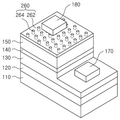
도 3은 본 발명의 제2 실시형태에 따른 투명 전극을 포함하는 반도체 발광 소자의 사시도이다.3 is a perspective view of a semiconductor light emitting element including a transparent electrode according to a second embodiment of the present invention.
도 3에서 보는 바와 같이, 본 발명의 제2 실시형태에 따른 상기 제2 투명 전극(260)은 제2 그래핀층(262)과, 일방향으로 등간격을 가지며 서로 다른 열과 지즈재그 형태로 배열된 제2 접촉층(264)를 포함한다.As shown in FIG. 3, the second
상기 제2 접촉층(264)은 상기 제2 그래핀층(262)과 상기 제2 그래핀층(262)의 하부에 위치한 p형 질화물 반도체층(150)과의 접촉성을 높이기 위하여 상기 제2 그래핀층(262)의 일부분에 상기 제2 그래핀층(262)을 관통하여 형성된다.
The
도 2 내지 도 3에 도시된 바와 같이, 상기 접촉층들(164, 264)은 원기둥 형태일 수 있으나. 삼각기둥, 사각기둥 육각기둥 등 다양한 형태로 이루어질 수 있음은 물론이다.As illustrated in FIGS. 2 to 3, the contact layers 164 and 264 may have a cylindrical shape. Of course, it can be made in a variety of forms, such as a triangular prism, square prism hexagonal pillar.
이상에서 설명한 바와 같이, 상기 접촉층은 일정한 패턴으로 형성될 수 있으나, 필요에 따라서는 간격이 서로 다른 랜덤 분포를 가질 수도 있다.
As described above, the contact layer may be formed in a predetermined pattern, but may have random distributions having different intervals as necessary.
도 4는 본 발명의 제3 실시형태에 따른 투명 전극을 나타낸 사시도이다.4 is a perspective view showing a transparent electrode according to a third embodiment of the present invention.
도 4에 도시된 바와 같이, 본 발명의 제3 실시형태에 따른 제3 투명 전극(360)은 제3 그래핀층(362)과 상기 제3 그래핀층(362)내에서 격자 패턴으로 형성된 상기 제3 접촉층(364)을 포함한다. As shown in FIG. 4, the third
상기 제3 접촉층(364)은 상기 제3 그래핀층(362)과 상기 제3 그래핀층(362)의 하부에 위치한 p형 질화물 반도체층(미도시)과의 접촉성을 높이기 위하여 상기 제3 그래핀층(362)의 일부분에 상기 제3 그래핀층(362)을 관통하여 형성된다.The
이와 같이 투명 전극의 그래핀층 내에 형성된 접촉층은 그래핀층의 접촉저항을 낮추기 위하여 다양한 형태로 형성될 수 있다.
As such, the contact layer formed in the graphene layer of the transparent electrode may be formed in various forms to lower the contact resistance of the graphene layer.
도 5을 참조하여 본 발명의 제4 실시형태에 따른 발광 소자에 대해 설명한다. The light emitting element which concerns on 4th Embodiment of this invention is demonstrated with reference to FIG.
도 5을 참조하면, 본 발명의 제4 실시형태에 따른 발광 소자(2)는 단파장 LED로서, 기판(110)과, 상기 기판(110) 상에 순차적으로 형성된 언도프 반도체층(120), n형 질화물 반도체층(130), 활성층(140) 및 p형 질화물 반도체층(150), 제4 투명 전극(460), n형 전극(170) 및 p형 전극(180)을 포함하여 구성된다.Referring to FIG. 5, the
이하 본 발명의 제1 실시형태에서와 동일한 구성에 대하여는 설명을 생략한다.Hereinafter, description is abbreviate | omitted about the structure similar to 1st Embodiment of this invention.
도 5에 도시된 바와 같이, 상기 제4 투명 전극(460)은, 상기 p형 질화물 반도체층(150) 상부의 일부에 형성된 제4 접촉층(464) 및 상기 제4 접촉층(464)과 상기 p형 질화물 반도체층(150)을 모두 덮도록 형성된 제4 그래핀층(462)을 포함하여 이루어져 있다.As illustrated in FIG. 5, the fourth
본 실시형태에서는 본 발명의 제1 실시형태와 달리 상기 제4 접촉층(464)이 제4 그래핀층(462)과 동일한 높이가 아니며, 상기 제4 그래핀층(462) 보다 낮은 높이로 형성되어 있다.In the present embodiment, unlike the first embodiment of the present invention, the
즉 상기 제4 접촉층(464)은 상기 제4 그래핀층(462)과 상기 제4 그래핀층(462)의 하부에 위치한 p형 질화물 반도체층(150)과의 접촉성을 높이기 위하여 상기 제4 그래핀층(462)의 하부 일부분에 형성된다.That is, the
또한 상기 제4 접촉층(464)은 투명 전극으로 사용되는 제4 그래핀층(462)의 접촉저항을 낮추고 상기 활성층(140)으로부터 출사되는 빛의 반사도를 높여 발광 효율을 높일 수 있는 금속, 합금, 또는 산화물 등으로 형성된다. 바람직하게는 상기 제4 접촉층(464)으로 은(Ag), 니켈-은(Ni-Ag)합금, 니켈-금(Ni-Au)합금, ITO 가 사용될 수 있다.특히 상기 제4 접촉층(464)은 은(Ag) 또는 니켈-은(Ni-Ag)합금으로 이루어지는 것이 더욱 바람직하다. In addition, the
이와 같이 접촉층을 덮도록 그래핀층을 형성하면, 투명 전극 내의 그래핀층의 비율이 본 발명의 제1 실시형태에서 보다 높아지게 되므로 광 투과성이 더 향상되는 효과가 있다.
When the graphene layer is formed so as to cover the contact layer in this way, the ratio of the graphene layer in the transparent electrode becomes higher than in the first embodiment of the present invention, so that the light transmittance is further improved.
도 6은 도 5에 도시된 제 4 투명 전극을 나타낸 사시도이다.FIG. 6 is a perspective view illustrating a fourth transparent electrode illustrated in FIG. 5.
도 6에 도시된 바와 같이, 상기 제4 접촉층(464)는 p형 질화물 반도체층(150)상에서 라인 패턴으로 배열된다. 즉 일방향으로 등간격을 갖는 다수의 제4 접촉층이 적어도 하나의 열을 이루어 배열된다.
As shown in FIG. 6, the
도 7은 본 발명의 제5 실시형태에 따른 투명 전극을 나타낸 사시도이다.7 is a perspective view showing a transparent electrode according to a fifth embodiment of the present invention.
도 7에 도시된 바와 같이, 제5 투명 전극(560)은 제5 그래핀층(562)과, 일방향으로 등간격을 가지며 서로 다른 열과 지즈재그 형태로 배열된 제5 접촉층(564)를 포함한다.As illustrated in FIG. 7, the fifth
상기 제5 접촉층(564)은 상기 제5 그래핀층(562)과 상기 제5 그래핀층(562)의 하부에 위치한 p형 질화물 반도체층(미도시)과의 접촉성을 높이기 위하여 상기 제5 그래핀층(562)의 하부 일부분에 형성된다.
The
그리고 도 6 및 도 7에 도시된 바와 같이, 상기 접촉층은 원기둥 형태일 수 있으나. 삼각기둥, 사각기둥, 육각기둥 등 다양한 형태로 이루어질 수 있음은 물론이다.
6 and 7, the contact layer may have a cylindrical shape. Of course, it can be made in various forms such as a triangular prism, a square prism, a hexagonal prism.
이상에서 설명한 바와 같이 상기 접촉층은 일정한 패턴으로 형성될 수 있으나, 필요에 따라서는 간격이 서로 다른 랜덤 분포를 가질 수도 있다. 또는 투명 전극을 그래핀층과 그래핀층 일부 하부에 격자 패턴으로 형성된 접촉층을 포함하여 형성할 수 있다. 이와 같이 투명 전극의 그래핀층 내에 형성된 접촉층은 그래핀층의 접촉저항을 낮추기 위하여 다양한 형태로 형성될 수 있다.
As described above, the contact layer may be formed in a predetermined pattern, but may have random distributions having different intervals as necessary. Alternatively, the transparent electrode may include a contact layer formed in a lattice pattern on the graphene layer and a part of the graphene layer. As such, the contact layer formed in the graphene layer of the transparent electrode may be formed in various forms to lower the contact resistance of the graphene layer.
본 발명의 다양한 실시형태는 수평구조의 발광소자에서 그래핀층을 포함하는 투명 전극을 사용하는 것에 대하여 설명하였으나, 수직구조, 플립칩 구조 등 다양한 형태의 반도체 발광 소자에서 투명 전극으로 본 발명의 투명 전극을 사용할 수 있음은 물론이다.
Various embodiments of the present invention have been described using a transparent electrode including a graphene layer in a light emitting device of a horizontal structure, but the transparent electrode of the present invention as a transparent electrode in various types of semiconductor light emitting device, such as a vertical structure, flip chip structure Of course it can be used.
이상, 본 발명을 바람직한 실시형태들을 들어 상세하게 설명하였으나, 본 발명은 상기 실시예들에 한정되지 않으며, 본 발명의 기술적 사상 내에서 당 분야의 통상의 지식을 가진 자에 의하여 여러 가지 많은 변형이 가능함은 명백하다. 본 발명의 실시예들은 예시적이고 비한정적으로 모든 관점에서 고려되었으며, 이는 그 안에 상세한 설명 보다는 첨부된 청구범위와, 그 청구범위의 균등 범위와 수단내의 모든 변형 예에 의해 나타난 본 발명의 범주를 포함시키려는 것이다.
As mentioned above, the present invention has been described in detail with reference to preferred embodiments, but the present invention is not limited to the above embodiments, and various modifications may be made by those skilled in the art within the technical spirit of the present invention. It is obvious. Embodiments of the invention have been considered in all respects as illustrative and not restrictive, including the scope of the invention as indicated by the appended claims rather than the detailed description therein, the equivalents of the claims and all modifications within the means. I want to.
110 ... 기판 120 ...언도프 반도체층
130 ...n형 질화물 반도체층 140 ...활성층
150 ...p형 질화물 반도체층 160 ...제1 투명 전극
162 ...제1 그래핀층 164 ...제1 접촉층
170 ...n형 전극 180 ...p형 전극
260 ...제2 투명 전극 262 ...제2 그래핀층
264 ...제2 접촉층
360 ...제3 투명 전극 362 ...제3 그래핀층
364 ...제3 접촉층
460 ...제4 투명 전극 462 ...제4 그래핀층
464 ...제4 접촉층
560 ...제5 투명 전극 562 ...제5 그래핀층
564 ...제5 접촉층110 ...
130 ... n-type
150 ... p-type
162 ...
170 ... n-
260 ... second
264 ... second contact layer
360 ... third
364 ... Third contact layer
460 ... fourth
464 ... fourth contact layer
560 ... fifth
564 ... Fifth Contact Layer
Claims (13)
상기 n형 반도체층과 서로 마주보게 형성된 p형 반도체층;
상기 n형 반도체층과 p형 반도체층 사이에 형성된 활성층; 및
상기 n형 반도체층 및 p형 반도체층 중 적어도 하나를 덮도록 형성되며, 그래핀층과 상기 그래핀층을 관통하는 접촉층으로 이루어진 전극;을 구비하는 반도체 발광 소자.
an n-type semiconductor layer;
A p-type semiconductor layer formed to face the n-type semiconductor layer;
An active layer formed between the n-type semiconductor layer and the p-type semiconductor layer; And
And an electrode formed to cover at least one of the n-type semiconductor layer and the p-type semiconductor layer, the electrode including a graphene layer and a contact layer penetrating through the graphene layer.
상기 접촉층은 금속, 합금 및 산화물로 이루어진 군에서 선택된 어느 하나의 물질로 이루어진 것을 특징으로 하는 반도체 발광 소자.
The method of claim 1,
The contact layer is a semiconductor light emitting device, characterized in that made of any one material selected from the group consisting of metals, alloys and oxides.
상기 접촉층은 은(Ag), 니켈-은(Ni-Ag)합금, 니켈-금(Ni-Au)합금, 및 ITO로 이루어진 군에서 선택된 어느 하나의 물질로 이루어진 것을 특징으로 하는 반도체 발광 소자.
The method of claim 1,
The contact layer is a semiconductor light emitting device, characterized in that made of any one material selected from the group consisting of silver (Ag), nickel-silver (Ni-Ag) alloy, nickel-gold (Ni-Au) alloy, and ITO.
상기 접촉층은 상기 그래핀층과 동일한 높이로 형성된 것을 특징으로 하는 반도체 발광 소자.
The method of claim 1,
The contact layer is a semiconductor light emitting device, characterized in that formed with the same height as the graphene layer.
상기 접촉층은 원기둥, 삼각기둥, 사각기둥 및 육각기둥으로 이루어진 군에서 선택된 어느 하나의 상을 갖는 것을 특징으로 하는 반도체 발광 소자.
The method of claim 1,
The contact layer has a semiconductor light emitting device, characterized in that it has any one phase selected from the group consisting of a cylinder, a triangular column, a square column and a hexagonal column.
상기 접촉층은 복수개로 이루어져 라인 패턴으로 배열된 것을 특징으로 하는 반도체 발광 소자.
The method of claim 1,
The contact layer is a plurality of semiconductor light emitting device, characterized in that arranged in a line pattern.
상기 접촉층은 격자 패턴으로 형성되는 것을 특징으로 하는 반도체 발광 소자.
The method of claim 1,
The contact layer is a semiconductor light emitting device, characterized in that formed in a grid pattern.
상기 n형 반도체층과 서로 마주보게 형성된 p형 반도체층;
상기 n형 반도체층과 p형 반도체층 사이에 형성된 활성층; 및
상기 n형 반도체층 및 p형 반도체층 중 적어도 하나를 덮도록 형성되며, 그래핀층과 접촉층으로 이루어지고, 상기 그래핀층은 상기 접촉층의 상부를 덮도록 형성된 전극; 을 구비하는 반도체 발광 소자.
an n-type semiconductor layer;
A p-type semiconductor layer formed to face the n-type semiconductor layer;
An active layer formed between the n-type semiconductor layer and the p-type semiconductor layer; And
An electrode formed to cover at least one of the n-type semiconductor layer and the p-type semiconductor layer, the graphene layer and a contact layer, and the graphene layer formed to cover an upper portion of the contact layer; And a semiconductor light emitting element.
상기 접촉층은 금속, 합금 및 산화물로 이루어진 군에서 선택된 어느 하나의 물질로 이루어진 것을 특징으로 하는 반도체 발광 소자.
9. The method of claim 8,
The contact layer is a semiconductor light emitting device, characterized in that made of any one material selected from the group consisting of metals, alloys and oxides.
상기 접촉층은 은(Ag), 니켈-은(Ni-Ag)합금, 니켈-금(Ni-Au)합금, 및 ITO로 이루어진 군에서 선택된 어느 하나의 물질로 이루어진 것을 특징으로 하는 반도체 발광 소자.
9. The method of claim 8,
The contact layer is a semiconductor light emitting device, characterized in that made of any one material selected from the group consisting of silver (Ag), nickel-silver (Ni-Ag) alloy, nickel-gold (Ni-Au) alloy, and ITO.
상기 접촉층은 원기둥, 삼각기둥, 사각기둥 및 육각기둥으로 이루어진 군에서 선택된 어느 하나의 상을 갖는 것을 특징으로 하는 반도체 발광 소자.
9. The method of claim 8,
The contact layer has a semiconductor light emitting device, characterized in that it has any one phase selected from the group consisting of a cylinder, a triangular column, a square column and a hexagonal column.
상기 접촉층은 복수개로 이루어져 라인 패턴으로 배열된 것을 특징으로 하는 반도체 발광 소자.
9. The method of claim 8,
The contact layer is a plurality of semiconductor light emitting device, characterized in that arranged in a line pattern.
상기 접촉층은 격자 패턴으로 형성되는 것을 특징으로 하는 반도체 발광 소자.
9. The method of claim 8,
The contact layer is a semiconductor light emitting device, characterized in that formed in a grid pattern.
Priority Applications (1)
| Application Number | Priority Date | Filing Date | Title |
|---|---|---|---|
| KR1020120033491A KR20130111031A (en) | 2012-03-30 | 2012-03-30 | Semiconductor light emitting device |
Applications Claiming Priority (1)
| Application Number | Priority Date | Filing Date | Title |
|---|---|---|---|
| KR1020120033491A KR20130111031A (en) | 2012-03-30 | 2012-03-30 | Semiconductor light emitting device |
Publications (1)
| Publication Number | Publication Date |
|---|---|
| KR20130111031A true KR20130111031A (en) | 2013-10-10 |
Family
ID=49632749
Family Applications (1)
| Application Number | Title | Priority Date | Filing Date |
|---|---|---|---|
| KR1020120033491A Withdrawn KR20130111031A (en) | 2012-03-30 | 2012-03-30 | Semiconductor light emitting device |
Country Status (1)
| Country | Link |
|---|---|
| KR (1) | KR20130111031A (en) |
Cited By (2)
| Publication number | Priority date | Publication date | Assignee | Title |
|---|---|---|---|---|
| KR20160147349A (en) * | 2015-06-15 | 2016-12-23 | 엘지이노텍 주식회사 | Light Emitting Device |
| CN108780828A (en) * | 2016-01-05 | 2018-11-09 | Lg伊诺特有限公司 | Semiconductor device |
-
2012
- 2012-03-30 KR KR1020120033491A patent/KR20130111031A/en not_active Withdrawn
Cited By (4)
| Publication number | Priority date | Publication date | Assignee | Title |
|---|---|---|---|---|
| KR20160147349A (en) * | 2015-06-15 | 2016-12-23 | 엘지이노텍 주식회사 | Light Emitting Device |
| CN108780828A (en) * | 2016-01-05 | 2018-11-09 | Lg伊诺特有限公司 | Semiconductor device |
| CN108780828B (en) * | 2016-01-05 | 2022-02-11 | 苏州乐琻半导体有限公司 | Semiconductor device |
| US11355672B2 (en) | 2016-01-05 | 2022-06-07 | Suzhou Lekin Semiconductor Co., Ltd. | Semiconductor device |
Similar Documents
| Publication | Publication Date | Title |
|---|---|---|
| KR101712049B1 (en) | Light emitting device | |
| KR100661614B1 (en) | Nitride-based semiconductor light emitting device and its manufacturing method | |
| KR101646664B1 (en) | Light emitting device, method for fabricating the light emitting device and light emitting device package | |
| KR20120083084A (en) | Nano lod light emitting device and method of manufacturing the same | |
| US20130134475A1 (en) | Semiconductor light emitting device | |
| CN103650175A (en) | Semiconductor light emitting device and manufacturing method thereof | |
| KR20130042784A (en) | Nitride semiconductor light emitting device | |
| US10770622B2 (en) | Light-emitting element and light-emitting element package comprising same | |
| KR20130011767A (en) | Light emitting device | |
| CN108305922B (en) | Nitride semiconductor structure and semiconductor light emitting element | |
| KR102264678B1 (en) | Light emitting diode comprising porous transparent electrode | |
| KR20110117963A (en) | Nitride semiconductor light emitting device and manufacturing method thereof | |
| CN103782399B (en) | Nitride semiconductor luminescent element | |
| KR20130111031A (en) | Semiconductor light emitting device | |
| US10553756B2 (en) | Light emitting device | |
| KR20110041683A (en) | Semiconductor light emitting device and method for manufacturing same | |
| KR102315594B1 (en) | Light emitting device and lighting system | |
| KR102237123B1 (en) | Light emitting device and lighting system | |
| KR20130007682A (en) | Light emitting device and method for fabricating the same | |
| KR20110091245A (en) | Semiconductor light emitting device and manufacturing method thereof | |
| KR101285527B1 (en) | Light emitting diode | |
| KR100988193B1 (en) | Light emitting device | |
| KR20070063720A (en) | Gallium Nitride Light Emitting Diode | |
| KR100723230B1 (en) | Nitride Semiconductor LEDs and LED Packages | |
| KR20130032201A (en) | Light emitting device |
Legal Events
| Date | Code | Title | Description |
|---|---|---|---|
| PA0109 | Patent application |
Patent event code: PA01091R01D Comment text: Patent Application Patent event date: 20120330 |
|
| N231 | Notification of change of applicant | ||
| PN2301 | Change of applicant |
Patent event date: 20120629 Comment text: Notification of Change of Applicant Patent event code: PN23011R01D |
|
| PG1501 | Laying open of application | ||
| PC1203 | Withdrawal of no request for examination | ||
| WITN | Application deemed withdrawn, e.g. because no request for examination was filed or no examination fee was paid |