KR20130104800A - Apparatus for driving light emitting diode - Google Patents
Apparatus for driving light emitting diode Download PDFInfo
- Publication number
- KR20130104800A KR20130104800A KR1020120026662A KR20120026662A KR20130104800A KR 20130104800 A KR20130104800 A KR 20130104800A KR 1020120026662 A KR1020120026662 A KR 1020120026662A KR 20120026662 A KR20120026662 A KR 20120026662A KR 20130104800 A KR20130104800 A KR 20130104800A
- Authority
- KR
- South Korea
- Prior art keywords
- light emitting
- driving voltage
- emitting device
- capacitor
- diode
- Prior art date
- Legal status (The legal status is an assumption and is not a legal conclusion. Google has not performed a legal analysis and makes no representation as to the accuracy of the status listed.)
- Withdrawn
Links
- 239000003990 capacitor Substances 0.000 claims description 51
- 230000000630 rising effect Effects 0.000 claims description 3
- 238000007599 discharging Methods 0.000 claims description 2
- 238000000034 method Methods 0.000 claims 11
- 208000002193 Pain Diseases 0.000 abstract 1
- 238000010586 diagram Methods 0.000 description 13
- 230000000694 effects Effects 0.000 description 3
- 239000003792 electrolyte Substances 0.000 description 3
- 230000004048 modification Effects 0.000 description 2
- 238000012986 modification Methods 0.000 description 2
- 239000003985 ceramic capacitor Substances 0.000 description 1
- 238000006243 chemical reaction Methods 0.000 description 1
- 230000000593 degrading effect Effects 0.000 description 1
Images


Classifications
-
- H—ELECTRICITY
- H05—ELECTRIC TECHNIQUES NOT OTHERWISE PROVIDED FOR
- H05B—ELECTRIC HEATING; ELECTRIC LIGHT SOURCES NOT OTHERWISE PROVIDED FOR; CIRCUIT ARRANGEMENTS FOR ELECTRIC LIGHT SOURCES, IN GENERAL
- H05B45/00—Circuit arrangements for operating light-emitting diodes [LED]
- H05B45/30—Driver circuits
- H05B45/395—Linear regulators
-
- H—ELECTRICITY
- H05—ELECTRIC TECHNIQUES NOT OTHERWISE PROVIDED FOR
- H05B—ELECTRIC HEATING; ELECTRIC LIGHT SOURCES NOT OTHERWISE PROVIDED FOR; CIRCUIT ARRANGEMENTS FOR ELECTRIC LIGHT SOURCES, IN GENERAL
- H05B45/00—Circuit arrangements for operating light-emitting diodes [LED]
- H05B45/30—Driver circuits
- H05B45/345—Current stabilisation; Maintaining constant current
-
- H—ELECTRICITY
- H05—ELECTRIC TECHNIQUES NOT OTHERWISE PROVIDED FOR
- H05B—ELECTRIC HEATING; ELECTRIC LIGHT SOURCES NOT OTHERWISE PROVIDED FOR; CIRCUIT ARRANGEMENTS FOR ELECTRIC LIGHT SOURCES, IN GENERAL
- H05B45/00—Circuit arrangements for operating light-emitting diodes [LED]
- H05B45/30—Driver circuits
- H05B45/37—Converter circuits
-
- H—ELECTRICITY
- H05—ELECTRIC TECHNIQUES NOT OTHERWISE PROVIDED FOR
- H05B—ELECTRIC HEATING; ELECTRIC LIGHT SOURCES NOT OTHERWISE PROVIDED FOR; CIRCUIT ARRANGEMENTS FOR ELECTRIC LIGHT SOURCES, IN GENERAL
- H05B45/00—Circuit arrangements for operating light-emitting diodes [LED]
- H05B45/30—Driver circuits
- H05B45/355—Power factor correction [PFC]; Reactive power compensation
-
- Y—GENERAL TAGGING OF NEW TECHNOLOGICAL DEVELOPMENTS; GENERAL TAGGING OF CROSS-SECTIONAL TECHNOLOGIES SPANNING OVER SEVERAL SECTIONS OF THE IPC; TECHNICAL SUBJECTS COVERED BY FORMER USPC CROSS-REFERENCE ART COLLECTIONS [XRACs] AND DIGESTS
- Y02—TECHNOLOGIES OR APPLICATIONS FOR MITIGATION OR ADAPTATION AGAINST CLIMATE CHANGE
- Y02B—CLIMATE CHANGE MITIGATION TECHNOLOGIES RELATED TO BUILDINGS, e.g. HOUSING, HOUSE APPLIANCES OR RELATED END-USER APPLICATIONS
- Y02B20/00—Energy efficient lighting technologies, e.g. halogen lamps or gas discharge lamps
- Y02B20/30—Semiconductor lamps, e.g. solid state lamps [SSL] light emitting diodes [LED] or organic LED [OLED]
Landscapes
- Circuit Arrangement For Electric Light Sources In General (AREA)
- Led Devices (AREA)
Abstract
본 발명은 발광 소자 구동장치에 관한 것으로, 교류 전압을 입력 받아 노이즈를 제거하여 출력하는 필터부, 필터부의 출력을 정류하여 구동 전압을 출력하는 정류부, 교류 전압에 대응하는 입력 전류의 노이즈를 제거하고, 구동 전압의 크기를 보상하여 발광 소자에 전달하는 보상부 및 발광 소자에 흐르는 전류를 일정하게 유지시키는 정전류부를 포함하여, 역률 및 전 고조파 왜율 특성을 향상시키고, 발광 소자를 정전류 구동함과 동시에 깜빡거림 현상을 억제할 수 있다.The present invention relates to a light emitting device driving apparatus, comprising: a filter unit for receiving an AC voltage and removing noise and outputting the rectifier; a rectifying unit for rectifying the output of the filter unit and outputting a driving voltage; and removing noise of an input current corresponding to the AC voltage. And a compensating part for compensating the magnitude of the driving voltage to the light emitting device and a constant current part for maintaining a constant current flowing in the light emitting device, thereby improving power factor and total harmonic distortion factor characteristics, and at the same time flickering the light emitting device with constant current driving. Stinging phenomenon can be suppressed.
Description
본 발명은 발광 소자 구동장치에 관한 것으로, 특히 교류전압에 의해 구동되는 발광 소자 구동장치에 관한 기술이다.
BACKGROUND OF THE
일반적으로 실내 또는 실외의 조명등으로 백열전구나 형광등이 많이 사용되고 있는데, 이러한 백열전구나 형광등은 수명이 짧아 자주 교환하여야 하는 문제가 있다. 이러한 문제를 해결하기 위하여 우수한 제어성, 빠른 응답속도, 높은 전기-광 변환효율, 긴 수명, 적은 소비전력 및 높은 휘도의 특성을 갖는 발광 다이오드(Light Emitting Diode)를 적용한 조명기구가 개발되고 있다.In general, incandescent lamps or fluorescent lamps are often used as indoor or outdoor lighting lamps. Such incandescent lamps or fluorescent lamps have a short lifetime and therefore require frequent replacement. In order to solve this problem, a lighting apparatus using light emitting diodes having excellent controllability, fast response speed, high electro-optical conversion efficiency, long life, low power consumption and high luminance has been developed.
이러한 발광 다이오드는 통상 수십 mA의 작은 전류에서 구동되므로, 발광 다이오드를 교류전압에 직접 연결하여 사용하는 경우, 전류가 제한되지 않기 때문에 교류전압이 변동하는 경우에 전류의 변동이 함께 커지게 되어 발광 다이오드가 쉽게 파손되는 문제점이 있었다. 따라서, 교류전압을 낮은 직류전압으로 바꾸어주는 AC/DC 컨버터 등을 이용하거나, 정류 회로 및 저항을 이용하여 전류를 제한하는 회로를 이용하고 있다.Since the light emitting diode is usually driven at a small current of several tens of mA, when the light emitting diode is directly connected to an AC voltage, the current is not limited because the current is not limited. There was a problem that is easily broken. Therefore, an AC / DC converter for converting an AC voltage into a low DC voltage or the like is used, or a circuit for limiting current using a rectifier circuit and a resistor is used.
도 1은 종래기술에 따른 발광 소자 구동장치를 도시한 회로도이다.1 is a circuit diagram showing a light emitting device driving apparatus according to the prior art.
도 1을 참조하면, 종래의 발광 소자 구동장치는 정류부(10), 커패시터(C1) 및 저항(R1)을 포함한다. 정류부(10)는 교류전압(Vac)을 입력받아 전파 정류하여 출력한다. 커패시터(C1)는 정류부(10)로부터 출력된 전압을 충전 및 방전한다. 저항(R1)은 정류부(10)로부터 출력된 전압 및 커패시터(C1)에 충전된 전압(Vc)에 대응하는 전류의 크기를 제한하여 발광 다이오드(L1)에 공급한다. Referring to FIG. 1, a conventional light emitting device driving apparatus includes a
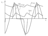
도 2는 종래기술에 따른 발광 소자 구동장치의 동작을 설명하기 위한 파형도이다.2 is a waveform diagram illustrating an operation of a light emitting device driving apparatus according to the prior art.
도 2를 참조하면, 교류전압(Vac)은 정류부(10)를 통해 전파 정류되어 출력된다. 그 다음, 정류부(10)로부터 출력된 전압이 발광 다이오드(L1)의 순방향 전압(Vf; Forward voltage) 이상이 되면 발광 다이오드(L1)에 저항(R1)을 거쳐 전류(Iled)가 흐른다. 이와 동시에, 커패시터(C1) 양단에 전압(Vc)이 충전되기 시작한다. 이때, 커패시터(C1)에는 교류전압(Vac)이 발광 다이오드(L1)의 순방향 전압(Vf) 이상이 되는 시점부터 전압(Vc)이 충전되고, 교류전압(Vac)이 하강하는 시점부터 전압(Vc)이 방전된다. 이에 따라, 입력전류(Iin)의 파형이 왜곡되어 역률(Power Factor) 및 전 고조파 왜율(Total Harmonics Distortion) 특성이 저하되는 문제점이 있다. 또한, 발광 다이오드(L1)에 흐르는 전류(Iled)의 리플(ripple)이 크게 나타나 발광 다이오드(L1)가 깜빡거리는(Flicker) 현상이 심하게 보이는 문제점이 있다. 이를 해결하기 위해 커패시터(C1)를 수십 μF의 용량을 갖는 전해질 커패시터를 이용하는 경우 회로의 크기가 커지고, 전해질 커패시터의 수명으로 인해 회로의 수명이 단축되는 문제점이 있다. Referring to FIG. 2, the AC voltage Vac is full-wave rectified through the
또한, 발광 다이오드(L1)에 정전류가 흐르도록 제어하기 위해 정전류 IC를 이용하는 경우 제어를 위한 별도의 정전류 제어회로가 필요하고, 가격이 상승하는 문제점이 있다.
In addition, when using a constant current IC to control the constant current flows to the light emitting diode (L1), a separate constant current control circuit for control is required, there is a problem that the price increases.
본 발명은 교류전압을 이용하여 발광 다이오드를 구동하는 발광 소자 구동장치의 역률, 전 고조파 왜율 및 전력 효율을 향상시키는데 그 목적이 있다.An object of the present invention is to improve the power factor, total harmonic distortion and power efficiency of a light emitting device driving apparatus for driving a light emitting diode using an AC voltage.
그리고, 본 발명은 적은 용량의 리플 필터용 커패시터를 이용하여 발광 소자의 깜빡거림 현상을 억제할 수 있도록 발광소자를 구동하는 전류를 가급적 직류에 가깝도록 만드는 데 그 목적이 있다. In addition, an object of the present invention is to make the current driving the light emitting device as close to the direct current as possible to suppress the flicker of the light emitting device using a small capacity capacitor for the ripple filter.
또한, 본 발명은 복잡한 스위칭 전원회로 또는 전류를 검출하여 되먹임하는 정전류 제어회로를 이용하지 않고 발광소자를 정전류로 구동할 수 있는 데 그 목적이 있다.
It is also an object of the present invention to drive a light emitting device with a constant current without using a complicated switching power supply circuit or a constant current control circuit that detects and feeds back a current.
본 발명은 교류 전압을 입력 받아 노이즈를 제거하여 출력하는 필터부; 상기 필터부의 출력을 정류하여 구동 전압을 출력하는 정류부; 상기 교류 전압에 대응하는 입력 전류의 노이즈를 제거하고, 상기 구동 전압의 크기를 보상하여 발광 소자에 전달하는 보상부; 및 상기 발광 소자에 흐르는 전류를 일정하게 유지시키는 정전류부를 포함한다. 여기서, 상기 보상부는 상기 필터부를 통해 흐르는 상기 입력 전류의 상승 및 하강 기울기를 보상하고, 상기 보상부는 상기 구동 전압을 충전 및 방전하여 상기 발광 소자의 발광 구간을 보상하며, 상기 보상부는 상기 발광 소자의 턴 오프 구간을 제거하는 것을 특징으로 한다. The present invention includes a filter unit for receiving an AC voltage to remove noise and output it; A rectifying unit rectifying the output of the filter unit to output a driving voltage; A compensator which removes noise of an input current corresponding to the AC voltage and compensates the magnitude of the driving voltage and transmits the magnitude of the driving voltage to the light emitting device; And a constant current unit for maintaining a constant current flowing through the light emitting device. Here, the compensation unit compensates the rising and falling slope of the input current flowing through the filter unit, the compensation unit to charge and discharge the driving voltage to compensate for the light emitting period of the light emitting device, the compensation unit of the light emitting device It characterized in that to remove the turn off period.
그리고, 상기 필터부는 저역 통과 필터를 포함하고, 상기 교류 전압은 제1 및 제2 교류 입력단자를 통해 입력되고, 상기 필터부는, 상기 제1 및 제2 교류 입력단자 각각에 연결된 제1 및 제2 저항; 및 상기 제1 및 제2 저항 사이에 연결된 제1 커패시터를 포함하는 것을 특징으로 한다. 또한, 상기 구동 전압은 제1 및 제2 구동 전압 출력단자를 통해 출력되고, 상기 정류부는, 상기 제1 구동전압 출력단자에 연결된 캐소드 단자와 상기 제1 커패시터의 일단에 연결된 애노드 단자를 포함하는 제1 다이오드; 상기 제1 구동전압 출력단자에 연결된 캐소드 단자와 상기 제1 커패시터의 타단에 연결된 제2 다이오드; 상기 제1 커패시터의 일단에 연결된 캐소드 단자와 상기 제2 구동전압 출력단자에 연결된 애노드 단자를 포함하는 제3 다이오드; 및 상기 제1 커패시터의 타단에 연결된 캐소드 단자와 상기 제2 구동전압 출력단자에 연결된 애노드 단자를 포함하는 제4 다이오드를 포함하는 것을 특징으로 한다. 상기 보상부는 상기 제1 및 제2 구동전압 출력단자 사이에 연결된 적어도 하나의 충방전 소자를 포함하는 것을 특징으로 한다. 상기 보상부는 상기 제2 구동전압 출력단자에 연결된 일단 및 상기 제2 다이오드의 애노드 단자와 상기 제4 다이오드의 캐소드 단자가 공통 접속된 노드에 연결된 타단을 포함하는 제2 커패시터; 및 상기 노드에 연결된 일단과 상기 제2 구동전압 출력단자에 연결된 타단을 포함하는 제3 커패시터를 포함하는 것을 특징으로 한다.The filter unit may include a low pass filter, and the AC voltage may be input through first and second AC input terminals, and the filter unit may include first and second connected to the first and second AC input terminals, respectively. resistance; And a first capacitor connected between the first and second resistors. The driving voltage may be output through first and second driving voltage output terminals, and the rectifying unit may include a cathode terminal connected to the first driving voltage output terminal and an anode terminal connected to one end of the first capacitor. 1 diode; A cathode diode connected to the first driving voltage output terminal and a second diode connected to the other end of the first capacitor; A third diode including a cathode terminal connected to one end of the first capacitor and an anode terminal connected to the second driving voltage output terminal; And a fourth diode including a cathode terminal connected to the other end of the first capacitor and an anode terminal connected to the second driving voltage output terminal. The compensation unit may include at least one charge / discharge device connected between the first and second driving voltage output terminals. The compensator includes a second capacitor including one end connected to the second driving voltage output terminal and the other end connected to a node to which an anode terminal of the second diode and a cathode terminal of the fourth diode are commonly connected; And a third capacitor including one end connected to the node and the other end connected to the second driving voltage output terminal.
그리고, 상기 정전류부는 상기 발광 소자에 연결된 정전류 다이오드를 포함하는 것을 특징으로 하고, 상기 정전류부는 상기 발광 소자에 흐르는 전류가 상기 구동 전압과 동일한 위상각의 전류 성분을 갖도록 보상하는 전류 보상 소자를 더 포함하는 것을 특징으로 하며, 상기 전류 보상 소자는 상기 정전류 소자와 병렬 연결된 저항을 포함하는 것을 특징으로 한다.
The constant current unit may include a constant current diode connected to the light emitting device, and the constant current unit further includes a current compensation device configured to compensate for a current flowing through the light emitting device to have a current component having a phase angle equal to the driving voltage. The current compensating device may include a resistor connected in parallel with the constant current device.
본 발명은 역률, 전 고조파 왜율 및 전력 효율을 향상시킬 수 있는 효과를 제공한다. The present invention provides the effect of improving the power factor, total harmonic distortion and power efficiency.
그리고, 본 발명은 적은 용량의 리플 필터용 커패시터를 이용하여 발광 소자의 깜빡거림 현상을 억제하고, 발광다이오드를 구동하는 전류의 첨두치를 낮춤으로서 LED 수명을 향상시킬 수 있는 효과를 제공한다. In addition, the present invention provides an effect of suppressing the flicker of the light emitting device by using a capacitor for a small capacity ripple filter and improving the LED lifetime by lowering the peak value of the current driving the light emitting diode.
또한, 본 발명은 스위칭 전원회로 또는 복잡한 되먹임 정전류 제어회로를 사용하지 않고 발광 소자를 정전류로 구동하여 발광 소자 구동장치를 소형화시킬 수 있는 효과를 제공한다.
In addition, the present invention provides the effect of miniaturizing the light emitting device driving apparatus by driving the light emitting device at a constant current without using a switching power supply circuit or a complex feedback constant current control circuit.
도 1은 종래기술에 따른 발광 소자 구동장치를 도시한 회로도.
도 2는 종래기술에 따른 발광 소자 구동장치의 문제점을 설명하기 위한 파형도.
도 3은 본 발명의 일 실시 예에 따른 발광 소자 구동장치를 도시한 회로도.
도 4는 본 발명의 일 실시 예에 따른 발광 소자 구동장치의 동작을 설명하기 위한 파형도.
도 5는 본 발명의 다른 실시 예에 따른 발광 소자 구동장치를 도시한 회로도.
도 6은 본 발명의 다른 실시 예에 따른 발광 소자 구동장치의 동작을 설명하기 위한 파형도.1 is a circuit diagram showing a light emitting device driving apparatus according to the prior art.
Figure 2 is a waveform diagram for explaining the problem of the light emitting device driving apparatus according to the prior art.
3 is a circuit diagram showing a light emitting device driving apparatus according to an embodiment of the present invention.
4 is a waveform diagram illustrating an operation of a light emitting device driving apparatus according to an embodiment of the present invention.
5 is a circuit diagram showing a light emitting device driving apparatus according to another embodiment of the present invention.
6 is a waveform diagram illustrating an operation of a light emitting device driving apparatus according to another exemplary embodiment of the present invention.
이하, 첨부된 도면을 참조하여 본 발명에 따른 실시 예들을 상세히 설명하기로 한다.Hereinafter, exemplary embodiments of the present invention will be described in detail with reference to the accompanying drawings.
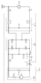
도 3은 본 발명의 일 실시 예에 따른 발광 소자 구동장치를 도시한 회로도이다. 3 is a circuit diagram illustrating a light emitting device driving apparatus according to an embodiment of the present invention.
도 3을 참조하면, 본 발명의 발광 소자 구동장치(100)는 필터부(110), 정류부(120), 보상부(130) 및 정전류부(140)를 포함한다. 필터부(110)는 제1 교류 입력단자(A1) 및 제2 교류 입력단자(A2)를 통해 교류전압(Vac)을 입력받아 노이즈를 제거하여 출력한다. 여기서, 제2 교류 입력단자(A2)는 접지단자(GND)에 연결되어 있다. 구체적으로, 필터부(110)는 제1 저항(R11), 제2 저항(R12) 및 제1 커패시터(C11)를 포함한다. 제1 저항(R11)은 제1 교류 입력단자(A1)와 제1 커패시터(C11)의 일단 사이에 연결되어 있고, 제2 저항(R12)은 제2 교류 입력단자(A2)와 커패시터(C11)의 타단 사이에 연결되어 있다. 여기서, 제1 및 제2 저항(R11, R12)은 수백 Ω 이내의 크기를 갖는 것이 바람직하다. 본 발명의 실시 예에 따른 제1 및 제2 저항(R11, R12)과 제1 커패시터(C11)는 저역 통과 필터(LPF; Low Pass Filter)를 구성할 수 있다. 또한, 제1 및 제2 저항(R11, R12)과 제2 및 제3 커패시터(C12, C13)는 입력전류(Iin)의 리플을 제거하기 위한 구성일 수 있다. 이에 대한 설명은 이하에서 자세히 설명한다. Referring to FIG. 3, the light emitting
그리고, 정류부(120)는 필터부(110)를 통해 교류전압(Vac)을 입력받아 정류하여 제1 및 제2 구동전압 출력단자(B1, B2)를 통해 구동전압(Vrec)을 출력한다. 이를 위해, 정류부(120)는 제1 내지 제4 다이오드(D1~D4)로 구성되는 전파 정류 회로를 포함한다. 여기서, 제1 다이오드(D1)는 제1 구동전압 출력단자(B1)에 연결된 캐소드 단자와 제1 커패시터(C11)의 일단에 연결된 애노드 단자를 포함한다. 제2 다이오드(D2)는 제1 구동전압 출력단자(B1)에 연결된 캐소드 단자와 제1 커패시터(C11)의 타단에 연결된 애노드 단자를 포함한다. 제3 다이오드(D3)는 제1 커패시터(C11)의 일단에 연결된 캐소드 단자와 제2 구동전압 출력단자(B2)에 연결된 애노드 단자를 포함한다. 제4 다이오드(D4)는 제1 커패시터(C11)의 타단에 연결된 캐소드 단자와 제2 구동전압 출력단자(B2)에 연결된 애노드 단자를 포함한다.The
보상부(130)는 구동전압(Vrec)을 충전 및 방전하여 발광 소자(L11)의 발광 구간을 보상한다. 또한, 보상부(130)는 필터부(110)를 통해 흐르는 입력전류(Iin)의 상승 및 하강 기울기를 보상하여 입력전류(Iin)의 리플을 완화시킨다. 이를 위해, 보상부(130)는 제2 및 제3 커패시터(C12, C13)를 포함한다. 여기서, 제2 커패시터(C12)는 제2 구동전압 출력단자(B1)에 연결된 일단과, 제2 다이오드(D2)의 애노드 단자와 제4 다이오드(D4)의 캐소드 단자가 공통 접속된 노드(N1)에 연결된 타단을 포함한다. 제3 커패시터(C13)는 노드(N1)에 연결된 일단과 제2 구동전압 출력단자(B2)에 연결된 타단을 포함한다. 본 발명의 실시 예에 따른 제2 및 제3 커패시터(C12, C13)는 수 μF의 크기를 갖는 적층 세라믹 커패시터(MLCC; Multi-Layer Ceramic Capacitor)로 구성하는 것이 바람직하다. 이 경우 종래의 전해질 커패시터에 비해 수명에 제한이 적고, 회로를 소형화하여 구성할 수 있다.The
한편, 본 발명의 실시 예에서는 보상부(130)를 2개의 커패시터로 구성하는 경우를 예를 들어 설명하였으나, 본 발명은 이에 한정되지 않고, 제1 및 제2 구동전압 출력단자(B1, B2) 사이에 연결된 1개의 커패시터를 이용할 수 있다. Meanwhile, in the exemplary embodiment of the present invention, the case in which the
그리고, 정전류부(140)는 발광 소자(L11)에 일정한 크기의 전류(Iled)가 흐르도록 제어한다. 이를 위해, 정전류부(140)는 정전류 소자(J1) 및 제3 저항(R13)을 포함한다. 정전류 소자(J1)는 발광 소자(L11)에 직렬 연결되어 있는 애노드 단자와 제3 저항(R13)의 일단에 연결된 캐소드 단자를 포함한다. 본 발명의 실시 예에 따른 정전류 소자(J1)는 정전류 다이오드(CRD; Current Regulative Diode)를 포함한다. 정전류 다이오드는 입력 전압, 온도 등의 변화에 대응하여 일정한 전류를 공급하는 특성을 가지며, 별도의 스위칭 소자가 필요없어 회로를 간단하게 구성할 수 있다. 그러나, 본 발명의 실시 예는 이에 한정되지 않으며, 정전류 소자(J1)를 FET 등의 다른 소자를 이용하여 구성할 수 있다. 제3 저항(R13)의 타단은 제2 구동전압 출력단자(B2)에 연결되어 있다. 제3 저항(R13)은 정전류 소자(J1) 양단에 걸리는 전압의 크기를 제한하여 정전류 소자(J1)가 안정적으로 동작하도록 한다. 본 발명은 이에 한정되지 않고, 제3 저항(R13) 대신 다이오드를 이용할 수 있고, 제3 저항(R13)을 생략할 수도 있다. In addition, the constant
한편, 도 3에 도시된 발광 소자(L11)는 발광 다이오드를 포함하며, 설명 상의 편의를 위해 1개의 발광 다이오드만 도시하였으나, 본 발명은 이에 한정되지 않으며, 발광 다이오드의 개수는 변경 가능하며, 복수의 발광 다이오드가 직렬 또는 병렬 연결될 수 있다. 또한, 본 발명의 실시 예에 따른 발광 다이오드(L11)는 백색 발광 다이오드인 것이 바람직하다. 그러나, 본 발명은 이에 한정되지 않고, 백색이 아닌 적색, 청색, 녹색, 노란색 등을 발광하는 발광 다이오드를 포함할 수 있다. Meanwhile, the light emitting device L11 illustrated in FIG. 3 includes a light emitting diode, and only one light emitting diode is illustrated for convenience of description. However, the present invention is not limited thereto, and the number of light emitting diodes may be changed. The light emitting diodes of may be connected in series or in parallel. In addition, the light emitting diode L11 according to the embodiment of the present invention is preferably a white light emitting diode. However, the present invention is not limited thereto and may include a light emitting diode that emits red, blue, green, yellow, and the like instead of white.
도 4는 본 발명의 일 실시 예에 따른 발광 소자 구동장치의 동작을 설명하기 위한 파형도이다. 도 4의 (a)는 도 3에 도시된 제2 및 제3 커패시터(C12, C13)의 용량이 발광소자(L11)의 순방향 전압(Vf) 보다 큰 경우를 도시한 도면이고, (b)는 제2 및 제3 커패시터(C12, C13)의 용량이 발광소자(L11)의 순방향 전압(Vf) 보다 작은 경우를 도시한 도면이다.4 is a waveform diagram illustrating an operation of a light emitting device driving apparatus according to an embodiment of the present invention. FIG. 4A is a diagram illustrating a case where the capacitances of the second and third capacitors C12 and C13 shown in FIG. 3 are larger than the forward voltage Vf of the light emitting element L11, and FIG. The case where the capacitances of the second and third capacitors C12 and C13 are smaller than the forward voltage Vf of the light emitting element L11 is illustrated.
도 4를 참조하면, 교류전압(Vac)이 제1 교류 입력단자(A1) 및 제2 교류 입력단자(A2)를 통해 필터부(110)에 입력된다. 먼저, 교류전압(Vac)의 양(+)의 반주기 동안 교류전압(Vac)은 제1 저항(R11) 및 제1 커패시터(C11)를 통해 고주파 성분이 제거되어 출력된다. 그 다음, 교류전압(Vac)은 제1 다이오드(D1) 및 제4 다이오드(D4)에 의해 정류되어 제1 및 제2 구동전압 출력단자(B1, B2)를 통해 구동전압(Vrec)이 출력된다. 이와 동시에, 제2 커패시터(C12) 양단에 일정 전압이 충전되기 시작한다. 이에 따라, 구동전압(Vrec)이 교류전압(Vac)의 실효치보다 높은 크기로 보상되어 구동전압(Vrec)이 발광 소자(L11)의 순방향 전압(Vf) 이상으로 상승되는 시점이 빨라진다. 즉, 구동전압(Vrec)이 발광 소자(L11)의 순방향 전압(Vf) 이상이 되는 구간이 길어져 발광 소자(L11)의 턴 온 구간이 증가한다.Referring to FIG. 4, the AC voltage Vac is input to the
그 다음, 발광 소자(L11)가 턴 온되어 전류(Iled)가 흐르기 시작하면, 전류(Iled)는 정전류 소자(J1)를 통해 일정한 크기로 제한된다. 그리고, 제2 커패시터(C12) 양단에 충전된 전압은 방전되기 시작한다. 여기서, 제2 커패시터(C12)의 용량이 발광 소자(L11)의 순방향 전압(Vf) 보다 큰 경우, 예컨대 4.7μF 이면 발광 소자(L11)에 흐르는 전류(Iled)가 도 4의 (a)에 도시된 바와 같이, 리플이 없는 직류 파형을 가진다. 반면, 제2 커패시터(C12)의 용량이 발광 소자(L11)의 순방향 전압(Vf) 보다 작은 경우, 예컨대 2.2μF 이면 발광 소자(L11)에 흐르는 전류(Iled)가 도 4의 (b)에 도시된 바와 같이, 일부 구간동안 리플 성분을 갖는다. 그러나, 이 경우에도 종래에 비해 리플 성분의 크기가 감소되었기 때문에 발광 소자(L11)가 깜빡거리는 현상이 억제될 수 있다. 또한, 발광 소자(L11)가 턴 오프되는 구간이 제거되어 발광 효율이 증가할 수 있다.Then, when the light emitting element L11 is turned on and the current Iled starts to flow, the current Iled is limited to a constant size through the constant current element J1. Then, the voltage charged across the second capacitor C12 starts to be discharged. Here, when the capacitance of the second capacitor C12 is larger than the forward voltage Vf of the light emitting element L11, for example, 4.7 μF, the current Iled flowing in the light emitting element L11 is illustrated in FIG. 4A. As shown, it has a direct current waveform with no ripple. On the other hand, when the capacitance of the second capacitor C12 is smaller than the forward voltage Vf of the light emitting element L11, for example, 2.2 μF, the current Iled flowing in the light emitting element L11 is illustrated in FIG. 4B. As shown, it has a ripple component for some period. However, even in this case, since the size of the ripple component is reduced as compared with the related art, the phenomenon of flickering of the light emitting element L11 can be suppressed. In addition, since the section in which the light emitting device L11 is turned off is removed, the light emission efficiency may increase.
한편, 입력전류(Iin)는 교류전압(Vac)의 양(+)의 반주기 동안 제1 교류 입력단자(A1)부터 제1 저항(R11), 제1 다이오드(D1), 제1 및 제2 커패시터(C12, 13), 제4 다이오드(D4)를 거쳐 제2 교류 입력단자(A2) 방향으로 흐른다. 즉, 입력전류(Iin)는 제1 커패시터(C12)의 충전에 대응하여 천천히 상승하고, 발광소자(L11)의 턴 온에 의한 제1 커패시터(C12)의 방전에 대응하여 천천히 하강한다. 즉, 입력전류(Iin)가 교류전압(Vac)의 파형과 유사한 형태로 흐른다. 이로 인해, 역률(Power Factor) 및 전 고조파 왜율(Total Harmonics Distortion) 특성이 향상될 수 있다.On the other hand, the input current (Iin) is the first resistor R11, the first diode (D1), the first and second capacitors from the first AC input terminal (A1) during the half period of the positive (+) of the AC voltage (Vac) (C12, 13), and flows in the direction of the second AC input terminal A2 via the fourth diode D4. That is, the input current Iin slowly rises in response to the charging of the first capacitor C12, and slowly falls in response to the discharge of the first capacitor C12 by turning on the light emitting element L11. That is, the input current Iin flows in a form similar to the waveform of the AC voltage Vac. As a result, power factor and total harmonic distortion characteristics may be improved.
그 다음, 교류전압(Vac)의 음(-)의 반주기 동안에도 위에서 설명한 내용과 동일하게 동작한다. 결국, 구동전압(Vrec)은 제2 및 제3 커패시터(C12, C13)에 의해 보상되어 발광 소자(L11)의 턴 오프 구간은 제거되고, 리플이 억제된 턴 온 구간이 증가한다. Next, the same operation as described above is performed even during the negative half period of the AC voltage Vac. As a result, the driving voltage Vrec is compensated by the second and third capacitors C12 and C13 so that the turn-off period of the light emitting element L11 is eliminated, and the turn-on period in which ripple is suppressed increases.
도 5는 본 발명의 다른 실시 예에 따른 발광 소자 구동장치를 도시한 회로도이다. 도 5에 도시된 발광 소자 구동장치(100_1)의 필터부(110), 정류부(120) 및 보상부(130)는 도 3에 도시된 구성과 동일하여 동일한 도면 부호로 도시하였으며, 이에 대한 설명은 생략한다. 여기서, 도 5의 정전류부(140_1)는 정전류 소자(J1)와 병렬 연결된 전류 보상 소자를 더 포함하는 구성이 도 3과 다르다.5 is a circuit diagram illustrating a light emitting device driving apparatus according to another exemplary embodiment of the present invention. The
여기서, 본 발명의 다른 실시 예에 따른 전류 보상 소자는 제4 저항(R14)을 포함한다. 제4 저항(R14)은 발광 소자(L11)에 연결된 일단과 제2 구동전압 출력단(B2)에 연결된 타단을 포함한다. 제4 저항(R14)에는 구동전압(Vrec)의 위상각과 동일하고, 저항 값에 대응하는 크기를 갖는 전류가 흐른다. 즉, 발광 소자(L11)에는 정전류 소자(J1)를 통해 흐르는 전류와 제4 저항(R14)을 통해 흐르는 전류가 더해진 전류(Iled)가 흐른다. 예컨대, 발광 소자(L11)에 40mA의 전류가 흐르도록 구성한 경우, 정전류 소자(J1)를 통해 흐르는 전류가 30mA이고, 제4 저항(R14)에 흐르는 전류가 10mA가 되도록 할 수 있다.Here, the current compensation device according to another embodiment of the present invention includes a fourth resistor (R14). The fourth resistor R14 includes one end connected to the light emitting element L11 and the other end connected to the second driving voltage output terminal B2. A current having a magnitude equal to the phase angle of the driving voltage Vrec and corresponding to the resistance value flows through the fourth resistor R14. That is, the current Iled, to which the current flowing through the constant current device J1 and the current flowing through the fourth resistor R14 is added, flows through the light emitting device L11. For example, when the current of 40 mA flows through the light emitting element L11, the current flowing through the constant current element J1 may be 30 mA, and the current flowing through the fourth resistor R14 may be 10 mA.
도 6은 본 발명의 다른 실시 예에 따른 발광 소자 구동장치의 동작을 설명하기 위한 파형도이다. 도 6에 도시된 교류전압(Vac), 입력전류(Iin), 구동전압(Vrec)은 도 4와 동일하여 이에 대한 설명은 생략하며, 이하에서는 발광 소자(L11)에 흐르는 전류(Iled)에 대해 설명한다.6 is a waveform diagram illustrating an operation of a light emitting device driving apparatus according to another exemplary embodiment of the present invention. The AC voltage Vac, the input current Iin, and the driving voltage Vrec shown in FIG. 6 are the same as in FIG. 4, and description thereof is omitted. Hereinafter, the current Iled flowing through the light emitting element L11 will be described. Explain.
도 6을 참조하면, 구동전압(Vrec)이 발광 소자(L11)의 순방향 전압(Vf) 보다 커지면 발광 소자(L11)가 턴 온되어 전류가 흐르기 시작한다. 이때, 정전류 소자(J1)는 전류의 크기를 일정하게 유지시킨다. 이와 동시에, 제4 저항(R14)에도 전류가 흐르기 시작한다. 결국, 발광 소자(L11)에 흐르는 전류(Iled)는 구동전압(Vrec)과 유사한 형태의 전류 성분을 포함한다. 이로 인해, 발광 소자 구동장치의 전력 효율이 향상될 수 있다. Referring to FIG. 6, when the driving voltage Vrec is greater than the forward voltage Vf of the light emitting device L11, the light emitting device L11 is turned on and current starts to flow. At this time, the constant current element J1 keeps the magnitude of the current constant. At the same time, current also begins to flow in the fourth resistor R14. As a result, the current Iled flowing in the light emitting element L11 includes a current component in a form similar to the driving voltage Vrec. As a result, the power efficiency of the light emitting device driving apparatus can be improved.
이상 본 발명을 상기 실시 예들을 들어 설명하였으나, 본 발명은 이에 제한되는 것이 아니다. 당업자라면, 본 발명의 취지 및 범위를 벗어나지 않고 수정, 변경을 할 수 있으며 이러한 수정과 변경 또한 본 발명에 속하는 것임을 알 수 있을 것이다.
The present invention has been described above with reference to the above embodiments, but the present invention is not limited thereto. Those skilled in the art will appreciate that modifications and variations can be made without departing from the spirit and scope of the present invention and that such modifications and variations also fall within the present invention.
110: 필터부, 120: 구동전압 생성부
J1: 정전류 소자, R14: 전류 제한 소자110: filter unit, 120: driving voltage generation unit
J1: constant current device, R14: current limiting device
Claims (12)
상기 필터부의 출력을 정류하여 구동 전압을 출력하는 정류부;
상기 교류 전압에 대응하는 입력 전류의 노이즈를 제거하고, 상기 구동 전압의 크기를 보상하여 발광 소자에 전달하는 보상부; 및
상기 발광 소자에 흐르는 전류를 일정하게 유지시키는 정전류부
를 포함하는 발광 소자 구동장치.
A filter unit which receives an AC voltage and removes and outputs noise;
A rectifying unit rectifying the output of the filter unit to output a driving voltage;
A compensator which removes noise of an input current corresponding to the AC voltage and compensates the magnitude of the driving voltage and transmits the magnitude of the driving voltage to the light emitting device; And
Constant current unit for maintaining a constant current flowing through the light emitting element
Light emitting device driving apparatus comprising a.
상기 보상부는 상기 필터부를 통해 흐르는 상기 입력 전류의 상승 및 하강 기울기를 보상하는 것을 특징으로 하는 발광 소자 구동장치.
The method according to claim 1,
And the compensating part compensates for the rising and falling slope of the input current flowing through the filter part.
상기 보상부는 상기 구동 전압을 충전 및 방전하여 상기 발광 소자의 발광 구간을 보상하는 것을 특징으로 하는 발광 소자 구동장치.
The method according to claim 2,
And the compensator is configured to compensate for the light emission period of the light emitting device by charging and discharging the driving voltage.
상기 보상부는 상기 발광 소자의 턴 오프 구간을 제거하는 것을 특징으로 하는 발광 소자 구동장치.
The method according to claim 3,
And the compensator removes a turn-off period of the light emitting device.
상기 필터부는 저역 통과 필터를 포함하는 것을 특징으로 하는 발광 소자 구동장치.
The method according to claim 1,
And the filter part comprises a low pass filter.
상기 교류 전압은 제1 및 제2 교류 입력단자를 통해 입력되고,
상기 필터부는,
상기 제1 및 제2 교류 입력단자 각각에 연결된 제1 및 제2 저항; 및
상기 제1 및 제2 저항 사이에 연결된 제1 커패시터
를 포함하는 것을 특징으로 하는 발광 소자 구동장치.
The method according to claim 5,
The AC voltage is input through the first and second AC input terminals,
The filter unit includes:
First and second resistors connected to the first and second AC input terminals, respectively; And
A first capacitor connected between the first and second resistors
Light emitting device driving apparatus comprising a.
상기 구동 전압은 제1 및 제2 구동 전압 출력단자를 통해 출력되고,
상기 정류부는,
상기 제1 구동전압 출력단자에 연결된 캐소드 단자와 상기 제1 커패시터의 일단에 연결된 애노드 단자를 포함하는 제1 다이오드;
상기 제1 구동전압 출력단자에 연결된 캐소드 단자와 상기 제1 커패시터의 타단에 연결된 제2 다이오드;
상기 제1 커패시터의 일단에 연결된 캐소드 단자와 상기 제2 구동전압 출력단자에 연결된 애노드 단자를 포함하는 제3 다이오드; 및
상기 제1 커패시터의 타단에 연결된 캐소드 단자와 상기 제2 구동전압 출력단자에 연결된 애노드 단자를 포함하는 제4 다이오드
를 포함하는 것을 특징으로 하는 발광 소자 구동장치.
The method of claim 6,
The driving voltage is output through the first and second driving voltage output terminal,
The rectifying unit includes:
A first diode including a cathode terminal connected to the first driving voltage output terminal and an anode terminal connected to one end of the first capacitor;
A cathode diode connected to the first driving voltage output terminal and a second diode connected to the other end of the first capacitor;
A third diode including a cathode terminal connected to one end of the first capacitor and an anode terminal connected to the second driving voltage output terminal; And
A fourth diode including a cathode terminal connected to the other end of the first capacitor and an anode terminal connected to the second driving voltage output terminal;
Light emitting device driving apparatus comprising a.
상기 보상부는,
상기 제1 및 제2 구동전압 출력단자 사이에 연결된 적어도 하나의 충방전 소자를 포함하는 것을 특징으로 하는 발광 소자 구동장치.
The method of claim 7,
Wherein the compensation unit comprises:
And at least one charge / discharge device connected between the first and second drive voltage output terminals.
상기 보상부는,
상기 제2 구동전압 출력단자에 연결된 일단 및 상기 제2 다이오드의 애노드 단자와 상기 제4 다이오드의 캐소드 단자가 공통 접속된 노드에 연결된 타단을 포함하는 제2 커패시터; 및
상기 노드에 연결된 일단과 상기 제2 구동전압 출력단자에 연결된 타단을 포함하는 제3 커패시터
를 포함하는 것을 특징으로 하는 발광 소자 구동장치.
The method according to claim 8,
Wherein the compensation unit comprises:
A second capacitor including one end connected to the second driving voltage output terminal and the other end connected to a node to which an anode terminal of the second diode and a cathode terminal of the fourth diode are commonly connected; And
A third capacitor including one end connected to the node and the other end connected to the second driving voltage output terminal;
Light emitting device driving apparatus comprising a.
상기 정전류부는,
상기 발광 소자에 연결된 정전류 다이오드를 포함하는 것을 특징으로 하는 발광 소자 구동장치.
The method according to claim 1,
The constant current unit,
And a constant current diode connected to the light emitting device.
상기 정전류부는 상기 발광 소자에 흐르는 전류가 상기 구동 전압과 동일한 위상각의 전류 성분을 갖도록 보상하는 전류 보상 소자를 더 포함하는 것을 특징으로 하는 발광 소자 구동장치.
The method of claim 10,
The constant current unit further comprises a current compensating element for compensating for the current flowing through the light emitting element to have a current component of the same phase angle as the driving voltage.
상기 전류 보상 소자는 상기 정전류 소자와 병렬 연결된 저항을 포함하는 것을 특징으로 하는 발광 소자 구동장치.The method of claim 11,
And the current compensating element comprises a resistor connected in parallel with the constant current element.
Priority Applications (2)
| Application Number | Priority Date | Filing Date | Title |
|---|---|---|---|
| KR1020120026662A KR20130104800A (en) | 2012-03-15 | 2012-03-15 | Apparatus for driving light emitting diode |
| PCT/KR2013/002096 WO2013137678A1 (en) | 2012-03-15 | 2013-03-15 | Driving device for light-emitting device |
Applications Claiming Priority (1)
| Application Number | Priority Date | Filing Date | Title |
|---|---|---|---|
| KR1020120026662A KR20130104800A (en) | 2012-03-15 | 2012-03-15 | Apparatus for driving light emitting diode |
Publications (1)
| Publication Number | Publication Date |
|---|---|
| KR20130104800A true KR20130104800A (en) | 2013-09-25 |
Family
ID=49161500
Family Applications (1)
| Application Number | Title | Priority Date | Filing Date |
|---|---|---|---|
| KR1020120026662A Withdrawn KR20130104800A (en) | 2012-03-15 | 2012-03-15 | Apparatus for driving light emitting diode |
Country Status (2)
| Country | Link |
|---|---|
| KR (1) | KR20130104800A (en) |
| WO (1) | WO2013137678A1 (en) |
Cited By (1)
| Publication number | Priority date | Publication date | Assignee | Title |
|---|---|---|---|---|
| US9532412B2 (en) | 2014-10-22 | 2016-12-27 | Silicon Works Co., Ltd. | Lighting apparatus capable of reducing flicker |
Families Citing this family (2)
| Publication number | Priority date | Publication date | Assignee | Title |
|---|---|---|---|---|
| CN108541111B (en) * | 2018-05-30 | 2024-04-02 | 深圳市明微电子股份有限公司 | Constant-current output control circuit and method for LED lamp illumination driving and LED device |
| WO2025001950A1 (en) * | 2023-06-29 | 2025-01-02 | 苏州欧普照明有限公司 | Constant current driving circuit, constant current control system and lamp |
Family Cites Families (5)
| Publication number | Priority date | Publication date | Assignee | Title |
|---|---|---|---|---|
| US6459603B1 (en) * | 2001-04-02 | 2002-10-01 | International Business Machines Corporation | Adapter circuit for selectively doubling input voltage depending upon connector type |
| KR101759614B1 (en) * | 2009-09-01 | 2017-07-25 | 필립스 라이팅 홀딩 비.브이. | Power supply system for electronic loads |
| JP5198405B2 (en) * | 2009-10-22 | 2013-05-15 | フェニックス電機株式会社 | Power circuit |
| JP5507957B2 (en) * | 2009-10-22 | 2014-05-28 | フェニックス電機株式会社 | Power circuit |
| KR101073498B1 (en) * | 2011-07-04 | 2011-10-17 | (주)우도 | LED module device for advertising signboard |
-
2012
- 2012-03-15 KR KR1020120026662A patent/KR20130104800A/en not_active Withdrawn
-
2013
- 2013-03-15 WO PCT/KR2013/002096 patent/WO2013137678A1/en not_active Ceased
Cited By (1)
| Publication number | Priority date | Publication date | Assignee | Title |
|---|---|---|---|---|
| US9532412B2 (en) | 2014-10-22 | 2016-12-27 | Silicon Works Co., Ltd. | Lighting apparatus capable of reducing flicker |
Also Published As
| Publication number | Publication date |
|---|---|
| WO2013137678A1 (en) | 2013-09-19 |
Similar Documents
| Publication | Publication Date | Title |
|---|---|---|
| US7791285B2 (en) | High efficiency AC LED driver circuit | |
| US8847509B2 (en) | Light-emitting diode driving apparatus including charging/discharging capacitor | |
| EP2793534A1 (en) | Led driving device | |
| US10264635B2 (en) | Ripple suppression circuit and light emitting diode driver | |
| EP2496056B1 (en) | Constant-current-drive led module device | |
| KR20130072175A (en) | Backlight module and driving method thereof and display device using the same | |
| CN103152914B (en) | AC rectification circuit and AC rectification method for driving LED module | |
| US9325237B2 (en) | Power supply with charge pump and control method | |
| CN105792421A (en) | A bridgeless LED drive power supply | |
| US9380669B2 (en) | Low flicker LED driving circuit with high power factor | |
| EP2249470B1 (en) | Capacitance reducing method for a pulsed activiated device and associated devices | |
| KR20130104800A (en) | Apparatus for driving light emitting diode | |
| CN102711346B (en) | Electronic ballast with multiple outputs | |
| KR101092218B1 (en) | LED Driving Circuit using Sumple Current Source | |
| KR101493813B1 (en) | LED illumination device with energy conservation | |
| KR101756458B1 (en) | A/d converter for led lighting device | |
| US9622308B2 (en) | Lighting device, illumination device, and lighting fixture | |
| US8519638B2 (en) | Electronic ballast for a high intesity discharge lamp | |
| EP2560461A2 (en) | Power converter and a dimmable solid-state lighting device with the power converter | |
| US20130088161A1 (en) | Driving circuit of light emitting diode | |
| KR101777566B1 (en) | LED Lamp | |
| US20240306275A1 (en) | Low power converter for compensating mains voltage variation | |
| JP5319606B2 (en) | Lighting device | |
| KR200465924Y1 (en) | LED Power Supply Device for Power Factor Improvement | |
| KR20140102951A (en) | Led power supply and led lighting apparatus using the same |
Legal Events
| Date | Code | Title | Description |
|---|---|---|---|
| PA0109 | Patent application |
Patent event code: PA01091R01D Comment text: Patent Application Patent event date: 20120315 |
|
| PG1501 | Laying open of application | ||
| PC1203 | Withdrawal of no request for examination | ||
| WITN | Application deemed withdrawn, e.g. because no request for examination was filed or no examination fee was paid |