KR20130067177A - Compound and organic light emitting diode device using the same - Google Patents
Compound and organic light emitting diode device using the same Download PDFInfo
- Publication number
- KR20130067177A KR20130067177A KR1020110134052A KR20110134052A KR20130067177A KR 20130067177 A KR20130067177 A KR 20130067177A KR 1020110134052 A KR1020110134052 A KR 1020110134052A KR 20110134052 A KR20110134052 A KR 20110134052A KR 20130067177 A KR20130067177 A KR 20130067177A
- Authority
- KR
- South Korea
- Prior art keywords
- light emitting
- compound
- layer
- carboline
- organic light
- Prior art date
- Legal status (The legal status is an assumption and is not a legal conclusion. Google has not performed a legal analysis and makes no representation as to the accuracy of the status listed.)
- Withdrawn
Links
- 0 *c(cc1)cc(c2c3*=*C*=C2)c1[n]3-c(cc1)cc(c2c3)c1[n](*)c2ccc3N(C*=**=C1)c(ccc(*)c2)c2C1=C Chemical compound *c(cc1)cc(c2c3*=*C*=C2)c1[n]3-c(cc1)cc(c2c3)c1[n](*)c2ccc3N(C*=**=C1)c(ccc(*)c2)c2C1=C 0.000 description 3
Images


Classifications
-
- H—ELECTRICITY
- H10—SEMICONDUCTOR DEVICES; ELECTRIC SOLID-STATE DEVICES NOT OTHERWISE PROVIDED FOR
- H10K—ORGANIC ELECTRIC SOLID-STATE DEVICES
- H10K85/00—Organic materials used in the body or electrodes of devices covered by this subclass
- H10K85/60—Organic compounds having low molecular weight
- H10K85/649—Aromatic compounds comprising a hetero atom
- H10K85/657—Polycyclic condensed heteroaromatic hydrocarbons
- H10K85/6572—Polycyclic condensed heteroaromatic hydrocarbons comprising only nitrogen in the heteroaromatic polycondensed ring system, e.g. phenanthroline or carbazole
-
- C—CHEMISTRY; METALLURGY
- C07—ORGANIC CHEMISTRY
- C07F—ACYCLIC, CARBOCYCLIC OR HETEROCYCLIC COMPOUNDS CONTAINING ELEMENTS OTHER THAN CARBON, HYDROGEN, HALOGEN, OXYGEN, NITROGEN, SULFUR, SELENIUM OR TELLURIUM
- C07F15/00—Compounds containing elements of Groups 8, 9, 10 or 18 of the Periodic Table
- C07F15/0006—Compounds containing elements of Groups 8, 9, 10 or 18 of the Periodic Table compounds of the platinum group
- C07F15/0033—Iridium compounds
-
- H—ELECTRICITY
- H10—SEMICONDUCTOR DEVICES; ELECTRIC SOLID-STATE DEVICES NOT OTHERWISE PROVIDED FOR
- H10K—ORGANIC ELECTRIC SOLID-STATE DEVICES
- H10K50/00—Organic light-emitting devices
- H10K50/10—OLEDs or polymer light-emitting diodes [PLED]
- H10K50/14—Carrier transporting layers
- H10K50/16—Electron transporting layers
-
- H—ELECTRICITY
- H10—SEMICONDUCTOR DEVICES; ELECTRIC SOLID-STATE DEVICES NOT OTHERWISE PROVIDED FOR
- H10K—ORGANIC ELECTRIC SOLID-STATE DEVICES
- H10K85/00—Organic materials used in the body or electrodes of devices covered by this subclass
- H10K85/30—Coordination compounds
- H10K85/341—Transition metal complexes, e.g. Ru(II)polypyridine complexes
- H10K85/342—Transition metal complexes, e.g. Ru(II)polypyridine complexes comprising iridium
-
- H—ELECTRICITY
- H10—SEMICONDUCTOR DEVICES; ELECTRIC SOLID-STATE DEVICES NOT OTHERWISE PROVIDED FOR
- H10K—ORGANIC ELECTRIC SOLID-STATE DEVICES
- H10K85/00—Organic materials used in the body or electrodes of devices covered by this subclass
- H10K85/60—Organic compounds having low molecular weight
- H10K85/649—Aromatic compounds comprising a hetero atom
- H10K85/654—Aromatic compounds comprising a hetero atom comprising only nitrogen as heteroatom
-
- C—CHEMISTRY; METALLURGY
- C09—DYES; PAINTS; POLISHES; NATURAL RESINS; ADHESIVES; COMPOSITIONS NOT OTHERWISE PROVIDED FOR; APPLICATIONS OF MATERIALS NOT OTHERWISE PROVIDED FOR
- C09K—MATERIALS FOR MISCELLANEOUS APPLICATIONS, NOT PROVIDED FOR ELSEWHERE
- C09K2211/00—Chemical nature of organic luminescent or tenebrescent compounds
- C09K2211/18—Metal complexes
- C09K2211/185—Metal complexes of the platinum group, i.e. Os, Ir, Pt, Ru, Rh or Pd
Landscapes
- Chemical & Material Sciences (AREA)
- Physics & Mathematics (AREA)
- Engineering & Computer Science (AREA)
- Materials Engineering (AREA)
- Spectroscopy & Molecular Physics (AREA)
- Organic Chemistry (AREA)
- Optics & Photonics (AREA)
- Crystallography & Structural Chemistry (AREA)
- Inorganic Chemistry (AREA)
- Electroluminescent Light Sources (AREA)
Abstract
본 발명은 하기 화학식 1로 표시되는 화합물 또는 이를 사용하는 유기전계발광소자에 관한 것이다.
[화학식 1]

여기서, 상기 X, Y 및 Z 중 적어도 어느 하나는 질소로 이루어지고,
상기 R1은 치환되거나 치환되지 않은 방향족 화합물과 헤테로 방향족 화합물 및 실리콘 화합물에서 선택되고,
상기 R2 및 R3는 각각 독립적으로 치환되거나 치환되지 않은 방향족 화합물과 헤테로 방향족 화합물, 수소, 중수소, 실리콘 화합물 및 포스포릴(phoshporyl)에서 선택한다.The present invention relates to a compound represented by the following formula (1) or an organic light emitting device using the same.
[Formula 1]
Here, at least one of the X, Y and Z is made of nitrogen,
R 1 is selected from a substituted or unsubstituted aromatic compound, a heteroaromatic compound, and a silicon compound,
R 2 and R 3 are each independently selected from a substituted or unsubstituted aromatic compound and a heteroaromatic compound, hydrogen, deuterium, a silicon compound, and phosphoryl.
Description
본 발명은 유기전계발광소자에 관한 것으로, 보다 구체적으로 수명과 발광효율을 향상시킬 수 있는 화합물 및 이를 이용한 유기전계발광소자에 관한 것이다.
The present invention relates to an organic light emitting display device, and more particularly, to a compound capable of improving lifespan and luminous efficiency, and an organic light emitting display device using the same.
오늘날, 정보 통신 발달과 함께 표시장치가 급격하게 발전해오고 있다. 특히, 표시장치 중 유기전계발광소자는 자발광 소자로써, 별도의 백라이트 유닛을 구비하지 않아도 되므로, 다른 표시장치에 비해 얇게 형성하며 낮은 소비전력을 가질 수 있다.Today, display devices have been rapidly developed with the development of information and communication. In particular, the organic light emitting display device of the display device is a self-light emitting device, and does not have to be provided with a separate backlight unit, and thus may be formed thinner than other display devices and may have low power consumption.
여기서, 유기전계발광소자는 애노드 전극, 캐소드 전극 및 애노드 전극과 캐소드 전극 사이에 구비된 발광층을 포함한다. 여기서, 애노드 전극은 발광층에 정공을 제공하고, 캐소드 전극은 발광층에 전자를 제공한다. 이때, 발광층에서 전자와 정공의 재결합을 통해 엑시톤이 생성되며, 이 엑시톤이 기저상태로 떨어지면서 빛을 방출하게 된다.Here, the organic light emitting diode includes an anode electrode, a cathode electrode and a light emitting layer provided between the anode electrode and the cathode electrode. Here, the anode electrode provides holes to the light emitting layer, and the cathode electrode provides electrons to the light emitting layer. In this case, excitons are generated through recombination of electrons and holes in the emission layer, and the excitons fall to the ground state to emit light.
여기서, 엑시톤은 일중항과 삼중항의 비율이 1:3으로 존재할 수 있다. 이때, 형광의 경우 일중항의 엑시톤만을 이용하여 빛을 방출하게 되며, 인광의 경우 일중항과 삼중항의 엑시톤을 모두 이용하여 빛을 방출하게 된다. 이에 따라, 유기전계발광소자가 형광보다 인광 재료를 이용할 경우, 높은 발광효율을 얻을 수 있다. 이와 같이, 인광재료는 형광재료에 비해 매우 높은 양자효율을 가질 수 있으므로, 유기 전계 발광 소자의 발광 효율을 높일 수 있어, 많은 연구가 이루어지고 있다.Here, the exciton may have a ratio of the singlet and triplet is 1: 3. In this case, in the case of fluorescence, light is emitted using only the excitons of the singlet, and in the case of phosphorescence, light is emitted using both the excitons of the singlet and triplet. Accordingly, when the organic electroluminescent device uses a phosphorescent material rather than fluorescence, high luminous efficiency can be obtained. As described above, since the phosphorescent material may have a very high quantum efficiency as compared with the fluorescent material, the luminous efficiency of the organic EL device can be increased, and much research has been made.
한편, 인광 재료는 호스트 물질과 이로부터 에너지를 전이받아 발광하는 인광 도판트 물질을 포함할 수 있다. 이는, 인광 재료가 인광 도판트 단독으로 사용될경우, 소광현상으로 인해 발광효율이 급격하게 줄어들기 때문이다. 이때, 호스트 물질의 삼중항 에너지 레벨이 인광도판트의 삼중항 에너지 레벨보다 충분히 커야만 에너지 전이과정에서 역 에너지 전이발생없이 전이현상을 발생시킬 수 있다. 즉, 호스트 물질의 삼중항 에너지 레벨이 인광도판트의 삼중항 에너지 레벨보다 클 경우, 양자 효율을 최대로 이끌어낼 수 있다.Meanwhile, the phosphorescent material may include a host material and a phosphorescent dopant material which emits light by transferring energy therefrom. This is because when the phosphorescent material is used alone as a phosphorescent dopant, the luminous efficiency is drastically reduced due to the quenching phenomenon. At this time, the triplet energy level of the host material must be sufficiently larger than the triplet energy level of the phosphor, so that the transition phenomenon can occur without the reverse energy transfer in the energy transfer process. In other words, when the triplet energy level of the host material is greater than the triplet energy level of the phosphor, the quantum efficiency can be maximized.
하지만, 종래 호스트 물질의 삼중항 에너지 레벨은 인광도판트의 삼중항 에너지 레벨보다 작아, 양자효율을 향상시키는데 한계가 있었다. However, the triplet energy level of the conventional host material is smaller than the triplet energy level of the phosphorescent dopant, thereby limiting the improvement of the quantum efficiency.
종래 호스트 물질은 낮은 유리전이온도를 가짐에 따라, 재료의 열적 안정성의 영향을 주어 고온 또는 구동온도에서 재료의 변형으로 인한 소자의 수명이 단축되는 문제점이 있었다.As the conventional host material has a low glass transition temperature, there is a problem that the life of the device is shortened due to the deformation of the material at a high temperature or a driving temperature due to the thermal stability of the material.
따라서, 유기전계발광소자의 발광효율 및 수명을 향상시키기 위해, 새로운 호스트 재료의 개발이 시급하다.
Therefore, in order to improve the luminous efficiency and lifetime of the organic light emitting display device, it is urgent to develop a new host material.
본 발명은 유기전계발광소자에서 발생할 수 있는 문제점을 해결하기 위한 것으로, 구체적으로 발광효율 및 수명을 동시에 향상시킬 수 있는 화합물 및 이를 사용한 유기전계발광소자를 제공함에 그 목적이 있다.
The present invention is to solve the problems that may occur in the organic light emitting device, and in particular, an object of the present invention to provide a compound and an organic light emitting device using the same that can improve the luminous efficiency and lifetime.
본 발명에 따른 하나의 해결 수단의 화합물을 제공한다. 본 발명에 따른 화합물은 하기 화학식 1로 표시될 수 있다.One compound of one solution according to the invention is provided. Compounds according to the invention can be represented by the following formula (1).

여기서, 상기 X, Y 및 Z 중 적어도 어느 하나는 질소로 이루어지고, 상기 R1은 치환되거나 치환되지 않은 방향족 화합물과 헤테로 방향족 화합물 및 실리콘 화합물에서 선택되고, 상기 R2 및 R3는 각각 독립적으로 치환되거나 치환되지 않은 방향족 화합물과 헤테로 방향족 화합물, 수소, 중수소, 실리콘 화합물 및 포스포릴(phoshporyl)에서 선택될 수 있다.Herein, at least one of X, Y and Z is made of nitrogen, and R1 is selected from a substituted or unsubstituted aromatic compound, a heteroaromatic compound and a silicon compound, and R2 and R3 are each independently substituted or substituted Non-aromatic compounds and heteroaromatic compounds, hydrogen, deuterium, silicone compounds and phosphoryls.
본 발명에 따른 다른 하나의 해결 수단의 유기전계발광소자를 제공한다. 본 발명에 따른 유기전계발광소자는 양극과 음극 사이에 발광층을 포함하는 유기전계발광소자에 있어서, 상기 발광층은 도펀트 물질과 호스트 물질을 포함하고, 상기 호스트 물질은 하기 화학식 1로 표시될 수 있다.Provided are an organic light emitting display device according to another solution according to the present invention. The organic light emitting device according to the present invention includes an organic light emitting device including a light emitting layer between an anode and a cathode, wherein the light emitting layer includes a dopant material and a host material, and the host material may be represented by the following Chemical Formula 1.
[화학식 1][Formula 1]

여기서, 상기 X, Y 및 Z 중 적어도 어느 하나는 질소로 이루어지고, 상기 R1은 치환되거나 치환되지 않은 방향족 화합물과 헤테로 방향족 화합물 및 실리콘 화합물에서 선택되고, 상기 R2 및 R3는 각각 독립적으로 치환되거나 치환되지 않은 방향족 화합물과 헤테로 방향족 화합물, 수소, 중수소, 실리콘 화합물 및 포스포릴(phoshporyl)에서 선택될 수 있다.
Herein, at least one of X, Y and Z is made of nitrogen, and R1 is selected from a substituted or unsubstituted aromatic compound, a heteroaromatic compound and a silicon compound, and R2 and R3 are each independently substituted or substituted Non-aromatic compounds and heteroaromatic compounds, hydrogen, deuterium, silicone compounds and phosphoryls.
본 발명의 실시예에 따른 유기전계발광소자는 신규한 화합물을 이용하여 고효율 및 장수명을 달성할 수 있다.
The organic electroluminescent device according to the embodiment of the present invention can achieve high efficiency and long life by using a novel compound.
도 1은 본 발명의 실시예에 따른 유기전계발광소자의 단면도이다.
도 2는 본 발명의 실험예에 따른 화합물의 UV 스펙트럼, 상온 PL 스펙트럼 및 저온에서의 PL 스펙트럼을 보여주는 그래프이다.1 is a cross-sectional view of an organic light emitting display device according to an embodiment of the present invention.
2 is a graph showing the UV spectrum, the room temperature PL spectrum and the PL spectrum at low temperature of the compound according to the experimental example of the present invention.
이하, 본 발명의 제 1 실시예에 따른 화합물에 대해 구체적으로 설명하기로 한다.Hereinafter, the compound according to the first embodiment of the present invention will be described in detail.
본 발명에 따른 화합물은 하기 화학식 1로 표시될 수 있다.Compounds according to the invention can be represented by the following formula (1).
[화학식 1][Formula 1]

여기서, 상기 X, Y 및 Z 중 적어도 어느 하나는 질소로 이루어지고, 상기 R1은 치환되거나 치환되지 않은 방향족 화합물과 헤테로 방향족 화합물 및 실리콘 화합물에서 선택되고, 상기 R2 및 R3는 각각 독립적으로 치환되거나 치환되지 않은 방향족 화합물과 헤테로 방향족 화합물, 수소, 중수소, 실리콘 화합물 및 포스포릴(phoshporyl)에서 선택될 수 있다.
Herein, at least one of X, Y and Z is made of nitrogen, and R1 is selected from a substituted or unsubstituted aromatic compound, a heteroaromatic compound and a silicon compound, and R2 and R3 are each independently substituted or substituted Non-aromatic compounds and heteroaromatic compounds, hydrogen, deuterium, silicone compounds and phosphoryls.
구체적으로, 상기 X는 질소이고 상기 Y와 상기 Z는 각각 탄소로 이루어지는 알파 카볼린(α-carboline)기, 상기 Y는 질소이고 상기 X와 상기 Z은 각각 탄소로 이루어지는 베타 카볼린(β-carboline)기 및 상기 Z는 질소이고 상기 X와 상기 Y는 각각 탄소로 이루어지는 감마 카볼린(γ-carboline)기 중에서 하나가 선택될 수 있다. 여기서, 치화된 카볼린기는 모두 동일하거나 다를 수 있다.Specifically, X is nitrogen, and Y and Z are alpha-carboline groups each consisting of carbon, Y is nitrogen, and X and Z are each beta carboline consisting of carbon (β-carboline). ) And Z is nitrogen, and X and Y may each be selected from a gamma carboline group consisting of carbon. Here, all of the carboxyl groups can be the same or different.
또한, 상기 R1은 페닐(phenyl), 디벤조티오펜(dibenzothiphene), 디펜조퓨란(dibenzofuran), 테트라페닐실란(tetraphenylsilane), 피리딘(pyridine), 퀸놀린(quinoline), 아이소퀴놀린(isoquinoline), 피리미딘(pyrimidine) 및 이들의 치환체로 이루어진 군에서 선택될 수 있다. 또는, 상기 R1의 치환체는 알파 카볼린기, 베타 카볼린기, 감마 카볼린기, 플로렌(fluorene) 및 이들의 치환체로 이루어진 군에서 선택될 수 있다.In addition, the R1 is phenyl, dibenzothiphene, diphenfuran, dibenzofuran, tetraphenylsilane, pyridine, quinolin, isoquinoline, isoquinoline, pyri It may be selected from the group consisting of pyrimidine and their substituents. Alternatively, the substituent of R1 may be selected from the group consisting of alpha carboline group, beta carboline group, gamma carboline group, fluorene and fluorene.
또는, 상기 R1의 치환체는 하기 화학식 A1 내지 A9로 이루어진 군에서 선택될 수 있다.Alternatively, the substituent of R1 may be selected from the group consisting of Formulas A1 to A9.

상기 R2 및 R3는 각각 독립적으로 수소, 페닐(phenyl), 트라이페닐실란(triphenylsilane), 테트라페닐실란(tetraphenylsilane), 피리딘(pyridine), 퀸놀린(quinoline), 아이소퀴놀린(isoquinoline), 피리미딘(pyrimidine) 및 이들의 치환체로 이루어진 군에서 선택될 수 있다.R2 and R3 are each independently hydrogen, phenyl, triphenylsilane, tetraphenylsilane, pyridine, quinolin, isoquinoline, pyrimidine ) And their substituents.
여기서, 화학식 1로 나타내지는 화합물의 구체적인 예로서는 하기 화학식 B1 내지 B17 중 어느 하나로 표시될 수 있다. 그러나, 본발명의 실시예에서 이를 한정하는 것은 아니다.Here, specific examples of the compound represented by Formula 1 may be represented by any one of the following Formulas B1 to B17. However, the embodiment of the present invention is not limited thereto.


여기서, 상기 화학식 1로 표시되는 화합물은 카볼린기를 가짐에 따라, 종래의 비스(N-카보졸리)바이페닐)Bis(N-carbazolyl)biphenyl;CBP)보다 높은 삼중항 에너지 레벨을 가질 수 있다. 이에 따라, 상기 화학식 1로 표시되는 화합물을 발광층의 호스트 물질을 이용할 경우, 호스트에서 도판트로 역 에너지 전이 현상을 방지할 수 있어, 발광 효율, 특히 저온에서 발광효율이 저하되는 것을 방지할 수 있다. Here, the compound represented by Formula 1 may have a triplet energy level higher than that of conventional bis (N-carbozolyl) biphenyl) Bis (N-carbazolyl) biphenyl; CBP as it has a carboline group. Accordingly, when the compound represented by Chemical Formula 1 is used as the host material of the light emitting layer, it is possible to prevent the reverse energy transfer phenomenon from the host to the dopant, thereby preventing the luminous efficiency, particularly at low temperature, from being lowered.
또한, 종래보다 삼중항 에너지 레벨과 단일항 에너지 레벨의 차이를 줄일 수 있어, 유기전계발광소자의 제작시 발광효율 및 전압특성을 증대시킬 수 있다.In addition, since the difference between the triplet energy level and the singlet energy level can be reduced compared to the prior art, the luminous efficiency and voltage characteristics can be increased when fabricating the organic light emitting device.
상기 화학식 1로 표시되는 화합물은 종래의 비스(N-카보졸리)바이페닐)Bis(N-carbazolyl)biphenyl;CBP)보다 높은 유리전이온도를 가짐에 따라, 유기전계발광소자의 제작시 수명을 향상시킬 수 있다.Compound represented by Formula 1 has a higher glass transition temperature than conventional bis (N- carbozolyl) biphenyl) Bis (N-carbazolyl) biphenyl (CBP), thereby improving the lifespan during fabrication of the organic light emitting device You can.
상기 화학식 1로 표시되는 화합물은 양극성을 가짐에 따라, 발광층내에서 전자 또는 정공의 일탈을 줄일 수 있어 유기전계발광소자의 제작시 수명 및 발광효율을 증대시킬 수 있다.As the compound represented by Chemical Formula 1 has a bipolarity, it is possible to reduce the deviation of electrons or holes in the light emitting layer, thereby increasing the lifespan and luminous efficiency during fabrication of the organic light emitting device.
또한, 상기 화학식 1로 표시되는 화합물은 정공 저지층과 전자수송층등을 형성하는 재질로 이용될 수 있다.
In addition, the compound represented by Formula 1 may be used as a material for forming a hole blocking layer and an electron transport layer.
이하, 유기전계발광소자의 도면을 참고하여 상세하게 설명한다. 다음에 소개되는 실시예들은 당업자에게 본 발명의 사상이 충분히 전달될 수 있도록 하기 위해 예로서 제공되어지는 것이다. Hereinafter, with reference to the drawings of the organic light emitting device will be described in detail. The following embodiments are provided by way of example so that those skilled in the art can fully understand the spirit of the present invention.
따라서, 본 발명은 이하 설명되어지는 실시예들에 한정되지 않고 다른 형태로 구체화될 수도 있다. 그리고, 도면들에 있어서, 장치의 크기 및 두께 등은 편의를 위하여 과장되어 표현될 수도 있다. 명세서 전체에 걸쳐서 동일한 참조번호들은 동일한 구성요소들을 나타낸다.Therefore, the present invention is not limited to the embodiments described below, but may be embodied in other forms. In the drawings, the size and thickness of an apparatus may be exaggerated for convenience. Like numbers refer to like elements throughout.
도 1은 본 발명의 제 2 실시예에 따른 유기전계발광소자의 단면도이다.1 is a cross-sectional view of an organic light emitting display device according to a second exemplary embodiment of the present invention.
도 1을 참조하면, 본 발명의 실시예에 따른 유기전계발광소자(100)는 기판(110)상에 순차적으로 배치된 양극(120), 발광층(150), 음극(190)을 포함할 수 있다.Referring to FIG. 1, an organic light
여기서, 기판(110)으로 사용될 수 있는 재질의 예로서는 유리 또는 수지일 수 있다. 기판(110)이 수지로 형성될 경우, 수지는 다른 재질에 비해 발광층(150)으로 수분이나 산소 투과율이 작은 재질로 선택될 수 있다. 수지의 예로서는 폴로카보네이트, 폴리이미드, 폴리에틸렌테레프탈레이트, 폴리에틸렌나프탈레이트 등일 수 있다. 기판(110)은 리지드(rigid)하거나 플렉시블(flexible)할 수 있다.Here, an example of a material that may be used as the
양극(120)은 기판(110)상에 배치되어 있다. 양극(120)은 투명한 도전물질로 이루어질 수 있다. 양극(120)을 형성하는 재질의 예로서는 ITO 또는 IZO일 수 있다. The
발광층(150)은 양극(120) 상에 배치될 수 있다. 여기서, 발광층(150)은 녹색 또는 청색을 발광하는 물질로 이루어질 수 있다. The
발광층(150)이 청색을 발광할 경우, 발광층(150)은 청색 인광 도판트와 상기 청색 인광 도판트가 도핑된 청색 인광 호스트 물질을 포함할 수 있다. When the
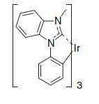
여기서, 청색 인광 도판트의 예로서는 하기 화학식 2 또는 화학식 3으로 표시되는 화합물로 선택될 수 있다. 그러나, 본 발명의 실시예에서, 청색 인광 도판트의 재질을 한정하는 것은 아니다.Here, as an example of the blue phosphorescent dopant, the compound represented by the following Chemical Formula 2 or Chemical Formula 3 may be selected. However, in the embodiment of the present invention, the material of the blue phosphorescent dopant is not limited.

또한, 청색 인광 호스트 물질은 상기 화학식 1로 표시되는 화합물일 수 있다. In addition, the blue phosphorescent host material may be a compound represented by Chemical Formula 1.
여기서, 청색 인광 호스트 물질과 청색 인광 도판트의 전체 중량을 기준으로 청색 인광 도판트는 0.1 내지 50중량%로 도핑될 수 있다. 여기서, 청색 인광 화합물이 0.1중량% 미만으로 도핑될 경우, 에너지 전환 효율이 작아질 수 있다. 반면, 청색 인광 화합물이 50중량%를 초과할 경우, 인광물질들간의 소광현상의 발생으로 인하여 발광 효율 및 수명이 떨어질 수 있다. Here, the blue phosphorescent dopant may be doped at 0.1 to 50% by weight based on the total weight of the blue phosphorescent host material and the blue phosphorescent dopant. Here, when the blue phosphorescent compound is doped at less than 0.1% by weight, the energy conversion efficiency may be reduced. On the other hand, when the blue phosphorescent compound exceeds 50% by weight, the luminous efficiency and lifespan may decrease due to the occurrence of quenching between the phosphors.
본 발명의 실시예에서, 유기발광층(140)은 청색 발광층인 것으로 설명하였으나, 실질적으로 풀컬러를 구현하기 위해, 유기발광층(140)은 영역별로 패턴화되어 있을 수 있으며, 청색 발광층 외에 녹색 발광층과 적색 발광층을 더 포함할 수 있다. 이때, 청색 발광층, 녹색 발광층 및 적색 발광층은 하나의 픽셀을 구성하여 여러가지 계조(grayscale)을 표현할 수 있다. 녹색 발광층을 구성하는 예로서는 호스트인 트리스-8-하이드록시퀴놀린 알루미늄(tris(8-hydroxyquinolino)aluminum;Alq3)과 녹색 인광 도판트인 N-메틸퀴인아크리돈(N-methylquinacridone;MQD)을 포함할 수 있다. 또한, 녹색 발광층의 두께는 300Å의 두께로 형성될 수 있다. 또한, 적색 발광층을 구성하는 예로서는 호스트인 4,4'-비스카바졸릴비페닐(4,4'-N,N'-dicarbazole-biphenyl;CBP)과 도판트인 비스(2-페닐퀴노린)아세틸아세토-네이트)이리듐(bis(2-phenylquinoline)(acetylaceto- nate)iridium;Ir(Phq)2(acac))포함할 수 있다. In the exemplary embodiment of the present invention, the organic
유기발광층(150)은 진공 증착법을 통해 형성될 수 있다.The organic
여기서, 녹색 발광층의 호스트 물질은 트리스-8-하이드록시퀴놀린 알루미늄(tris(8-hydroxyquinolino)aluminum;Alq3)로 형성하는 것으로 설명하였으나, 이에 한정되는 것은 아니며, 녹색 발광층의 호스트 물질은 상기 화학식 1로 표시되는 화합물을 이용할 수도 있다. 이때, 이에 따라, 청색 발광층과 녹색 발광층은 동일한 호스트 물질로 이루어질 수 있다.Here, the host material of the green light emitting layer is described as being formed of tris-8-hydroxyquinoline aluminum (Alq3), but is not limited thereto, and the host material of the green light emitting layer is represented by Chemical Formula 1 above. The compound shown can also be used. In this case, the blue light emitting layer and the green light emitting layer may be formed of the same host material.
음극(190)은 발광층(150) 상에 배치되어 있다. 음극(190)은 반사 도전물질로 이루어질 수 있다. 음극(190)을 형성하는 재질의 예로서는 Al, Ag, Cr, Au, W 및 Ti 중 어느 하나의 단일 금속 또는 어느 하나를 포함한 합금으로 이루어질 수 있다. 그러나, 본 발명의 실시예에서 음극(190)의 재질을 한정하는 것은 아니다.The
이에 더하여, 유기전계발광소자(100)는 양극(120)과 발광층(150) 사이에 배치되는 정공주입층(130)과 정공수송층(140)중 어느 하나 또는 둘을 모두 포함할 수 있다.In addition, the organic
여기서, 정공 주입층(130)은 양극(120)상에 배치될 수 있다. 이때, 정공 주입층(130)은 양극(120)으로부터 정공의 방출을 도와주는 역할을 할 수 있다. 정공 주입층을 형성하는 재질의 예로서는 4,4'-비스[N-[4-{N,N-비스(3-메틸페닐)아미노}페닐-N-페닐아미노]비페닐(4,4'-bis[4-{N,N-bis(3-methylphenyl)amino}phenyl}-N-phenylamino]biphenyl;DNTPD)일 수 있다. 여기서, 정공 주입층은 진공증착법을 통해 형성할 수 있다. 이때, 정공 주입층의 재질을 한정하는 것은 아니며, 다른 예로 4,4',4"-트리스(3-메틸페닐-N-페닐아미노)트리페닐아민)([4,4,4"-tris(3-methylphenylphenylamino)triphenylamine];m-MTDATA) 및 구리 프탈로시아닌(copper phthalocyanine;CuPc)등으로 형성될 수도 있다.Here, the
정공수송층(140)은 양극(120)으로부터 발광층(150)으로 원활하게 수송하는 역할을 할 수 있다. 여기서, 정공 수송층(140)은 발광층(150)으로부터 전자가 이탈하는 것을 방지하는 역할을 더 수행할 수 있다. 정공 수송층은 N,N-비스(나프탈렌-1-일)페닐-N,N-비스(페닐)벤지딘(N,N'-bis(naphthalene-1-yl)-N,N'- bis(phenyl)-benzidine;NPB)로 형성할 수 있다. The
여기서, 정공주입층(130)과 정공수송층(140)을 모두 구비할 경우, 정공주입층(130)과 정공수송층(140)은 양극(120)상에 순차적으로 적층되어 있을 수 있다.In this case, when the
이에 더하여, 유기전계발광소자(100)는 발광층(150) 및 음극(190) 사이에 배치된 정공저지층(160), 전자 수송층(170) 및 전자 주입층(180) 중 어느 하나 또는 둘을 모두 포함할 수 있다.In addition, the organic
여기서, 정공저지층(160)은 유기발광층(150)으로부터 정공이 이탈하는 것을 방지하는 역할을 할 수 있다. 정공 저지층(160)을 형성하는 물질의 예로서는 알루미늄(Ⅲ)비스(2-메틸-8-퀴톨리나토)-4-페닐페놀레이트(Aluminum(Ⅲ)bis(2-methyl-8-quinolinato)-4-phenylphenolate; BAlq)일 수 있다.Here, the
전자 수송층(170)은 음극(190)으로부터 방출된 전자를 발광층(150)으로 수송하는 역할을 할 수 있다. 여기서, 전자 수송층(170)은 발광층(150)에서 음극(190)으로 정공이 이탈하는 것을 방지하는 역할을 더 수행할 수 있다. 전자수송층(160)을 형성하는 재질의 예로서는 트리스(8-하이드로퀴놀리나토)알루미늄(Tris-8-hydroxyquinolinato aluminium;Alq3) 및 (2-(4-바이페닐)-5-(4-터트-부틸페닐)-1,3,4-옥사디아졸)(2-(4-biphenyl)-5-(4-tert-butylphenyl)-1,3,4-oxadiazole;PBD)등일 수 있다. The
전자 주입층(180)은 음극(190)으로부터 전자의 방출을 도와주는 역할을 할 수 있다. 여기서, 전자주입층(180)을 형성하는 물질의 예로서는 리튬 플로라이드(LiF)일 수 있다.The
본 발명의 실시예에서와 같이, 유기전계발광소자(100)는 발광층(150) 외에 정공 및 전자 주입층(120, 180), 정공저지층(160), 정공 및 전자 수송층(130, 170) 중 적어도 어느 하나를 더 포함함에 따라, 유기전계발광소자의 발광 효율 및 수명을 향상시킬 수 있다.As in the exemplary embodiment of the present invention, the organic
여기서, 정공저지층(160) 및 전자수송층(170) 중 적어도 어느 하나는 우수한 열안정을 갖는 상기 화학식 1로 표시되는 화합물로 이루어질 수 있다. Here, at least one of the
이에 더하여, 도면에는 도시되지 않았으나, 양극(120), 발광층(150) 및 음극(190)은 외부로부터 밀폐시키기 위한 밀봉부재를 더 구비할 수 있다. 이는 발광층(150)이 외부의 수분이나 산소에 의해 쉽게 열화될 수 있기 때문이다. 밀봉부재는 양극(120), 발광층(150) 및 음극(190)을 사이에 두고 기판과 마주하며 합착된 상부기판일 수 있다. 또는 밀봉부재는 양극(120), 발광층(150) 및 음극(190)을 포함한 기판(110)을 덮는 무기절연막일 수 있다.In addition, although not shown in the drawing, the
따라서, 본 발명의 실시예에서와 같이, 유기전계발광소자는 종래보다 높은 삼중항 에너지를 갖는 신규한 호스트 물질을 포함함에 따라, 유기전계발광소자의 발광 효율이 증대될 수 있다.Therefore, as in the embodiment of the present invention, the organic light emitting device includes a novel host material having a triplet energy higher than that of the prior art, thereby increasing the luminous efficiency of the organic light emitting device.
또한, 신규한 호스트 물질은 종래보다 높은 유리전이온도를 가짐에 따라, 고온 또는 구동온도에서 열에 의한 호스트 물질의 변형을 방지할 수 있어, 종래와 대비하여, 유기전계발광소자의 수명을 향상시킬 수 있다.In addition, since the new host material has a higher glass transition temperature than the conventional one, it is possible to prevent deformation of the host material due to heat at a high temperature or a driving temperature, thereby improving the lifetime of the organic light emitting device. have.
또한, 신규한 호스트 물질은 양극성을 가짐에 따라, 유기전계발광소자의 발광효율 및 수명특성을 증대시킬 수 있다.In addition, as the novel host material has bipolarity, the luminous efficiency and lifespan of the organic light emitting display device can be increased.
이하, 하기의 실험예들을 통해 본 발명에 따른 호스트 물질의 제조 방법에 대하여 구체적으로 설명하기로 한다. 하기의 실험예를 통해 본 발명을 설명하기 위한 것일 뿐 본 발명에 이에 한정되는 것은 아니다.
Hereinafter, a method of preparing a host material according to the present invention will be described in detail with reference to the following experimental examples. Through the following experimental example is only for illustrating the present invention is not limited thereto.
실험예Experimental Example 1 : 3,6-디(알파 1: 3,6-di (alpha 카볼린Kaboline )-9-(4-(() -9- (4-(( 트리페닐Triphenyl )실리)Silly) 페닐Phenyl )) 카바졸Carbazole (3,6-di(α-(3,6-di (α- carbolinecarboline )-9-(4-() -9- (4- ( triphenyl트리 피닐 )) silylphenlysilylphenly )) carbazolecarbazole )의 합성) Synthesis of
2구 플라스크에 1-요오드-(4-(트리페닐)실리)페닐(1-iodine-(4-(triphenyl)silylphenly) 3.24mmol, 3,6-디(알파 카볼린)카바졸(3,6-di(α-carboline)carbazole)3.24mmol, K3PO4 6.5mmol, CuI 0.97mmol,트렌스-1,2-사이클로헥산디아민(trans-1,2-cyclohexanediamine) 0.97mmol, 1,4-디옥산(1,4-dioxane) 50ml을 넣고, 질소 분위기 하에서 24시간동안 환류시켰다. 반응 종결 후, 1,4-디옥산(1,4-dioxane)을 감암 증류하여 제거하였다. 디클로로메탄(dichloromethane)과 물을 사용하여 추출한 후, 감압 증류하여 실리카 겔 칼럼(silica gel column)후 용매를 감압 증류한 후 디클로로메탄(dichloromethane)과 페토리움 에테르(petrolium ether)을 사용하여 재결정 및 필터링하여, 백색 파우더인 3,6-디(알파 카볼린)-9-(4-((트리페닐)실리)페닐)카바졸 1.0g을 얻었다.1-iodine- (4- (triphenyl) silyl) phenyl (1-iodine- (4- (triphenyl) silylphenly) 3.24 mmol, 3,6-di (alpha carboline) carbazole (3,6) -di (α-carboline) carbazole) 3.24 mmol, K 3 PO 4 6.5 mmol, CuI 0.97 mmol, trans-1,2-cyclohexanediamine 0.97 mmol, 1,4-dioxane 50 ml of (1,4-dioxane) was added and refluxed under a nitrogen atmosphere for 24 hours, and after completion of the reaction, 1,4-dioxane was removed by distillation under reduced pressure. After extraction with water, distillation under reduced pressure, silica gel column, and then the solvent was distilled under reduced pressure, and then recrystallized and filtered using dichloromethane and petrolium ether. 1.0 g of, 6-di (alpha carboline) -9- (4-((triphenyl) silyl) phenyl) carbazole was obtained.
3,6-디(알파 카볼린)-9-(4-((트리페닐)실리)페닐)카바졸의 합성 메카니즘은 하기 반응식 1로 표시될 수 있다.The synthesis mechanism of 3,6-di (alpha carboline) -9- (4-((triphenyl) silyl) phenyl) carbazole can be represented by Scheme 1 below.
[반응식1] [ Scheme 1]
이하, 도2 및 표1은 실험예 1로부터 제조된 화합물의 실험결과를 나타내었다. 2 and Table 1 show the experimental results of the compound prepared in Experimental Example 1.
도 2는 본 발명의 제조예에 따른 화합물의 UV 스펙트럼, 상온 PL 스펙트럼 및 저온에서의 PL 스펙트럼을 보여주는 그래프이다. 여기서, 저온은 77K이었다.Figure 2 is a graph showing the UV spectrum, room temperature PL spectrum and low temperature PL spectrum of the compound according to the preparation of the present invention. Here, the low temperature was 77K.
(℃)Tg
(℃)
(eV)HOMO a
(eV)
(eV)LUMO
(eV)
(eV)c E T
(eV) c
여기서, 상기 표 1에서 비교예는 J. Appl . Phys . 2001.90,5048에 기재하고 비스(N-카보졸리)바이페닐)Bis(N-carbazolyl)biphenyl;CBP)이다.Here, the comparative example in Table 1 is J. Appl . Phys . 2001.90,5048 and bis (N-carbozolyl) biphenyl) Bis (N-carbazolyl) biphenyl; CBP).
HOMO는 AC-2(Photo-electron spectrometer, RIKEN KEIKI CO., LTD)로 측정하였다.HOMO was measured by AC-2 (Photo-electron spectrometer, RIKEN KEIKI CO., LTD).
Band gap Energy는 UV absorption onset으로부터 측정하였다.Band gap energy was measured from UV absorption onset.
ET는 2-메틸 THF에 용해시킨 후 300nm에 대해서 PL maxima를 이용하여 exicitation을 측정하였다.E T was dissolved in 2-methyl THF and measured for exicitation using PL maxima for 300 nm.
상기 도 2 및 표1에서와 같이, 실험예 1에 의해 제조된 3,6-디(알파 카볼린)-9-(4-((트리페닐)실리)페닐)카바졸은 종래와 대비하여 높은 유리전이온도를 가짐을 확인할 수 있었다.As shown in FIG. 2 and Table 1, 3,6-di (alpha carboline) -9- (4-((triphenyl) silyl) phenyl) carbazole prepared by Experimental Example 1 was higher than that of the prior art. It was confirmed that the glass transition temperature.
실험예 1에 의해 제조된 3,6-디(알파 카볼린)-9-(4-((트리페닐)실리)페닐)카바졸은 종래 CBP와 대비하여 높은 삼중항 에너지 레벨을 가짐을 확인할 수 있었다.The 3,6-di (alpha carboline) -9- (4-((triphenyl) silyl) phenyl) carbazole prepared by Experimental Example 1 has a higher triplet energy level compared to the conventional CBP. there was.
또한, 실험예 1에 의해 제조된 3,6-디(알파 카볼린)-9-(4-((트리페닐)실리)페닐)카바졸은 종래 CBP와 대비하여 삼중항 에너지 레벨과 단일항 에너지 레벨의 차이가 작아지는 것을 확인할 수 있었다. 이에 따라, 실험예 1에 의해 제조된 3,6-디(알파 카볼린)-9-(4-((트리페닐)실리)페닐)카바졸은 종래에 비해 발광층으로의 전하의 진입 장벽이 낮아질 수 있다. In addition, the 3,6-di (alpha carboline) -9- (4-((triphenyl) silyl) phenyl) carbazole prepared by Experimental Example 1 has triplet energy level and singlet energy as compared to the conventional CBP. It was confirmed that the difference in level is small. Accordingly, the 3,6-di (alpha carboline) -9- (4-((triphenyl) silyl) phenyl) carbazole prepared in Experimental Example 1 has a lower barrier to entry of charge into the light emitting layer than in the prior art. Can be.
따라서, 종래와 대비하여 높은 유리전이 온도를 갖는 신규한 화합물을 이용하여 유기전계발광소자를 제조할 경우, 고온 또는 구동온도에서 열에 의한 호스트 물질의 변형을 방지할 수 있어, 유기전계발광소자의 수명을 향상시킬 수 있다.Therefore, when the organic light emitting diode is manufactured using a novel compound having a high glass transition temperature as compared with the conventional art, it is possible to prevent deformation of the host material due to heat at a high temperature or a driving temperature, and thus the lifetime of the organic light emitting diode. Can improve.
또한, 종래와 대비하여 높은 삼중항 에너지 레벨을 가지며, 낮은 단일항 에너지 레벨과 삼중항 에너지 레벨 차이를 갖는 신규한 화합물을 이용하여 유기전계발광소자를 제조할 경우, 유기전계발광소자의 발광효율 및 수명을 향상시킬 수 있다.
In addition, when the organic light emitting device is manufactured using a novel compound having a higher triplet energy level and a lower singlet energy level and a triplet energy level difference, the organic light emitting device has a high luminous efficiency and It can improve the service life.
110 : 기판
120 : 양극
130 : 정공주입층
140 : 정공수송층
150 : 발광층
160 : 정공저지층
170 : 전자수송층
180 : 전자주입층
190 : 음극110: substrate
120: anode
130: hole injection layer
140: hole transport layer
150: light emitting layer
160: hole blocking layer
170: electron transport layer
180: electron injection layer
190: cathode
Claims (13)
[화학식 1]

여기서, 상기 X, Y 및 Z 중 적어도 어느 하나는 질소로 이루어지고,
상기 R1은 치환되거나 치환되지 않은 방향족 화합물과 헤테로 방향족 화합물 및 실리콘 화합물에서 선택되고,
상기 R2 및 R3는 각각 독립적으로 치환되거나 치환되지 않은 방향족 화합물과 헤테로 방향족 화합물, 수소, 중수소, 실리콘 화합물 및 포스포릴(phoshporyl)에서 선택한다.
A compound represented by the following formula (1).
[Formula 1]
Here, at least one of the X, Y and Z is made of nitrogen,
R 1 is selected from a substituted or unsubstituted aromatic compound, a heteroaromatic compound, and a silicon compound,
R 2 and R 3 are each independently selected from a substituted or unsubstituted aromatic compound and a heteroaromatic compound, hydrogen, deuterium, a silicon compound, and phosphoryl.
상기 X는 질소이고 상기 Y와 상기 Z는 각각 탄소로 이루어지는 알파 카볼린(α-carboline)기, 상기 Y는 질소이고 상기 X와 상기 Z은 각각 탄소로 이루어지는 베타 카볼린(β-carboline)기 및 상기 Z는 질소이고 상기 X와 상기 Y는 각각 탄소로 이루어지는 감마 카볼린(γ-carboline)기 중에서 하나가 선택될 수 있으며,
치환된 카볼린기는 모두 동일하거나 다른 화합물.
The method of claim 1,
X is nitrogen, and Y and Z are alpha-carboline groups each consisting of carbon, Y is nitrogen, and X and Z are beta-carboline groups each consisting of carbon, and Z is nitrogen, and X and Y may each be selected from a gamma carboline group consisting of carbon,
Substituted carboline groups are all the same or different compounds.
상기 R1은 페닐(phenyl), 디벤조티오펜(dibenzothiphene), 디펜조퓨란(dibenzofuran), 테트라페닐실란(tetraphenylsilane), 피리딘(pyridine), 퀸놀린(quinoline), 아이소퀴놀린(isoquinoline), 피리미딘(pyrimidine) 및 이들의 치환체로 이루어진 군에서 선택된 화합물.
The method of claim 1,
The R1 is phenyl, dibenzothiphene, dibenzofuran, diphenylfuran, tetraphenylsilane, pyridine, quinolin, isoquinoline, pyrimidine pyrimidine) and substituents thereof.
상기 R1의 치환체는 알파 카볼린기, 베타 카볼린기, 감마 카볼린기, 플로렌(fluorene) 및 이들의 치환체로 이루어진 군에서 선택된 화합물.
The method of claim 3, wherein
The substituent of R1 is selected from the group consisting of alpha carboline group, beta carboline group, gamma carboline group, fluorene (fluorene) and substituents thereof.
상기 R1의 치환체는 하기 화학식 A1 내지 A9로 이루어진 군에서 선택된 화합물.

The method of claim 3, wherein
Substituent of R1 is a compound selected from the group consisting of the formula A1 to A9.
상기 R2 및 R3는 각각 독립적으로 수소, 페닐(phenyl), 트라이페닐실란(triphenylsilane), 테트라페닐실란(tetraphenylsilane), 피리딘(pyridine), 퀸놀린(quinoline), 아이소퀴놀린(isoquinoline), 피리미딘(pyrimidine) 및 이들의 치환체로 이루어진 군에서 선택된 화합물.
The method of claim 1,
R2 and R3 are each independently hydrogen, phenyl, triphenylsilane, tetraphenylsilane, pyridine, quinolin, isoquinoline, pyrimidine ) And substituents thereof.
상기 화학식 1은 하기 화학식 B1 내지 B17 중 어느 하나로 표시되는 화합물.


The method of claim 1,
Formula 1 is a compound represented by any one of the following formulas B1 to B17.
상기 발광층은 도펀트 물질과 호스트 물질을 포함하고,
상기 호스트 물질은 상기 제 1 항 내지 제 7 항 중 어느 한 항의 화합물로 이루어지는 유기전계발광소자.
In the organic light emitting device comprising a light emitting layer between the anode and the cathode,
The emission layer includes a dopant material and a host material,
The host material is an organic electroluminescent device comprising the compound of any one of claims 1 to 7.
상기 도펀트 물질은 하기 화학식 2 또는 화학식 3으로 표시되는 화합물에서 선택되는 유기전계발광소자.
[화학식 2]

[화학식 3]

The method of claim 8,
The dopant material is an organic light emitting display device selected from the compounds represented by the following formula (2) or (3).
(2)
(3)
상기 호스트 물질 및 상기 도펀트 물질의 전체 중량을 기준으로 상기 도펀트 물질은 0.1 내지 50 중량%를 함유하는 유기전계발광소자.
The method of claim 8,
The organic light emitting device of claim 1, wherein the dopant material contains 0.1 to 50% by weight based on the total weight of the host material and the dopant material.
상기 화학식 1로 표시되는 화합물은 청색 인광 호스트 물질 또는 녹색 인광 호스트 물질인 유기전계발광소자.
The method of claim 8,
The compound represented by Formula 1 is an organic electroluminescent device which is a blue phosphorescent host material or a green phosphorescent host material.
상기 양극과 상기 발광층 사이에 정공주입층과 정공수송층 중 어느 하나 또는 둘을 모두 포함하고, 상기 발광층과 상기 음극 사이에 정공저지층, 전자수송층과 전자주입층 중 어느 하나 또는 둘을 모두 포함하는 유기전계발광소자.
The method of claim 8,
An organic material including any one or both of a hole injection layer and a hole transport layer between the anode and the light emitting layer, and one or both of a hole blocking layer, an electron transport layer and an electron injection layer between the light emitting layer and the cathode; Electroluminescent element.
상기 정공저지층 및 전자수송층 중 적어도 어느 하나는 상기 제 1 항 내지 제 7 항 중 어느 한 항의 화합물로 이루어지는 유기전계발광소자.13. The method of claim 12,
At least one of the hole blocking layer and the electron transport layer is an organic electroluminescent device comprising the compound of any one of claims 1 to 7.
Priority Applications (1)
| Application Number | Priority Date | Filing Date | Title |
|---|---|---|---|
| KR1020110134052A KR20130067177A (en) | 2011-12-13 | 2011-12-13 | Compound and organic light emitting diode device using the same |
Applications Claiming Priority (1)
| Application Number | Priority Date | Filing Date | Title |
|---|---|---|---|
| KR1020110134052A KR20130067177A (en) | 2011-12-13 | 2011-12-13 | Compound and organic light emitting diode device using the same |
Publications (1)
| Publication Number | Publication Date |
|---|---|
| KR20130067177A true KR20130067177A (en) | 2013-06-21 |
Family
ID=48863139
Family Applications (1)
| Application Number | Title | Priority Date | Filing Date |
|---|---|---|---|
| KR1020110134052A Withdrawn KR20130067177A (en) | 2011-12-13 | 2011-12-13 | Compound and organic light emitting diode device using the same |
Country Status (1)
| Country | Link |
|---|---|
| KR (1) | KR20130067177A (en) |
Cited By (7)
| Publication number | Priority date | Publication date | Assignee | Title |
|---|---|---|---|---|
| US9634259B2 (en) | 2014-03-11 | 2017-04-25 | Samsung Display Co., Ltd. | Condensed cyclic compound and organic light-emitting device including the same |
| CN106916170A (en) * | 2015-12-28 | 2017-07-04 | 上海大学 | A kind of carboline disubstituted derivatives and its preparation method and application |
| WO2018103746A1 (en) * | 2016-12-08 | 2018-06-14 | 广州华睿光电材料有限公司 | Carbazole benzene fused ring derivative, polymer, mixture, composition, organic electronic device and preparation method therefor |
| WO2019100582A1 (en) * | 2017-11-24 | 2019-05-31 | 南京邮电大学 | Organic nano-grid, nano-polymer thereof and preparation method therefor |
| CN113121572A (en) * | 2019-12-30 | 2021-07-16 | 陕西莱特光电材料股份有限公司 | Heterocyclic compound, organic electroluminescent device, and electronic apparatus |
| US11873311B2 (en) | 2019-12-30 | 2024-01-16 | Shaanxi Lighte Optoelectronics Material Co., Ltd. | Heterocyclic compound, organic electroluminescent device, and electronic device |
| US12167677B2 (en) | 2021-03-19 | 2024-12-10 | Samsung Electronics Co., Ltd. | Heterocyclic compound and organic light-emitting device including the same |
-
2011
- 2011-12-13 KR KR1020110134052A patent/KR20130067177A/en not_active Withdrawn
Cited By (9)
| Publication number | Priority date | Publication date | Assignee | Title |
|---|---|---|---|---|
| US9634259B2 (en) | 2014-03-11 | 2017-04-25 | Samsung Display Co., Ltd. | Condensed cyclic compound and organic light-emitting device including the same |
| CN106916170A (en) * | 2015-12-28 | 2017-07-04 | 上海大学 | A kind of carboline disubstituted derivatives and its preparation method and application |
| WO2018103746A1 (en) * | 2016-12-08 | 2018-06-14 | 广州华睿光电材料有限公司 | Carbazole benzene fused ring derivative, polymer, mixture, composition, organic electronic device and preparation method therefor |
| CN109790117A (en) * | 2016-12-08 | 2019-05-21 | 广州华睿光电材料有限公司 | Carbazole benzene fused ring derivatives, polymers, mixtures, compositions, organic electronic devices and preparation methods thereof |
| WO2019100582A1 (en) * | 2017-11-24 | 2019-05-31 | 南京邮电大学 | Organic nano-grid, nano-polymer thereof and preparation method therefor |
| US11312717B2 (en) | 2017-11-24 | 2022-04-26 | Nanjing University Of Posts And Telecommunications | Organic nano-grid, nano-polymer thereof and preparation method therefor |
| CN113121572A (en) * | 2019-12-30 | 2021-07-16 | 陕西莱特光电材料股份有限公司 | Heterocyclic compound, organic electroluminescent device, and electronic apparatus |
| US11873311B2 (en) | 2019-12-30 | 2024-01-16 | Shaanxi Lighte Optoelectronics Material Co., Ltd. | Heterocyclic compound, organic electroluminescent device, and electronic device |
| US12167677B2 (en) | 2021-03-19 | 2024-12-10 | Samsung Electronics Co., Ltd. | Heterocyclic compound and organic light-emitting device including the same |
Similar Documents
| Publication | Publication Date | Title |
|---|---|---|
| EP2388842B1 (en) | Organic electroluminescent element | |
| JP6361138B2 (en) | Light emitting element | |
| KR101738607B1 (en) | Organic electroluminescent device | |
| CN102754237B (en) | Organic electroluminescent element | |
| US8859109B2 (en) | Compound for organic electroluminescent device and organic electroluminescent device using the same | |
| CN104953037B (en) | Organic light-emitting diode | |
| KR101195863B1 (en) | Aromatic Compounds and Organic Electroluminescent Devices Using the Same | |
| KR101957902B1 (en) | New compounds and organic light-emitting diode including the same | |
| WO2013122082A1 (en) | Light-emitting element material, and light-emitting element | |
| KR20110041728A (en) | Aromatic Compounds and Organic Electroluminescent Devices Using the Same | |
| KR102081595B1 (en) | Phosphorescent host compound and Organic electroluminescent device using the same | |
| KR20130067177A (en) | Compound and organic light emitting diode device using the same | |
| KR102237159B1 (en) | Organic Compound and Organic Light Emitting Diode Devices using the same | |
| US20170040546A1 (en) | Novel compound and organic electronic device using the same | |
| KR101601679B1 (en) | Compound Containing 5-Membered Heterocycle And Organic Electronic Element Using The Same, Terminal Thereof | |
| KR101555155B1 (en) | Novel spyrobifluorene type organic compounds and an organic electroluminescent device comprising the same | |
| CN105669555B (en) | Organic light-emitting display device | |
| KR102038815B1 (en) | Host compound for phosphorescent dopant and organic light emitting diode device using the same | |
| KR102004385B1 (en) | New compounds and organic light-emitting diode including the same | |
| KR102044134B1 (en) | Phosphorescent compound and Organic light emitting diode device using the same | |
| KR102489360B1 (en) | Compound for organic electronic element, organic electronic element comprising the same, and electronic device thereof | |
| KR101497123B1 (en) | Compound Containing 5-Membered Heterocycle And Organic Electronic Element Using The Same, Terminal Thereof | |
| KR20130015370A (en) | Phosphorescent material and organic electroluminescent device using the same | |
| KR101193522B1 (en) | Naphthalene derivatives and organic light-emitting diode including the same | |
| JP2014093501A (en) | Light-emitting element material and light emitting element |
Legal Events
| Date | Code | Title | Description |
|---|---|---|---|
| PA0109 | Patent application |
Patent event code: PA01091R01D Comment text: Patent Application Patent event date: 20111213 |
|
| PG1501 | Laying open of application | ||
| PC1203 | Withdrawal of no request for examination | ||
| WITN | Application deemed withdrawn, e.g. because no request for examination was filed or no examination fee was paid |