KR20130027153A - Control method of nonvolitile memory device - Google Patents
Control method of nonvolitile memory device Download PDFInfo
- Publication number
- KR20130027153A KR20130027153A KR1020110090542A KR20110090542A KR20130027153A KR 20130027153 A KR20130027153 A KR 20130027153A KR 1020110090542 A KR1020110090542 A KR 1020110090542A KR 20110090542 A KR20110090542 A KR 20110090542A KR 20130027153 A KR20130027153 A KR 20130027153A
- Authority
- KR
- South Korea
- Prior art keywords
- wear
- memory cells
- memory
- index
- wear ring
- Prior art date
- Legal status (The legal status is an assumption and is not a legal conclusion. Google has not performed a legal analysis and makes no representation as to the accuracy of the status listed.)
- Withdrawn
Links
Images


Classifications
-
- G—PHYSICS
- G11—INFORMATION STORAGE
- G11C—STATIC STORES
- G11C16/00—Erasable programmable read-only memories
- G11C16/02—Erasable programmable read-only memories electrically programmable
- G11C16/06—Auxiliary circuits, e.g. for writing into memory
- G11C16/10—Programming or data input circuits
- G11C16/14—Circuits for erasing electrically, e.g. erase voltage switching circuits
-
- G—PHYSICS
- G11—INFORMATION STORAGE
- G11C—STATIC STORES
- G11C16/00—Erasable programmable read-only memories
- G11C16/02—Erasable programmable read-only memories electrically programmable
- G11C16/06—Auxiliary circuits, e.g. for writing into memory
- G11C16/26—Sensing or reading circuits; Data output circuits
-
- G—PHYSICS
- G11—INFORMATION STORAGE
- G11C—STATIC STORES
- G11C16/00—Erasable programmable read-only memories
- G11C16/02—Erasable programmable read-only memories electrically programmable
- G11C16/06—Auxiliary circuits, e.g. for writing into memory
- G11C16/34—Determination of programming status, e.g. threshold voltage, overprogramming or underprogramming, retention
- G11C16/3436—Arrangements for verifying correct programming or erasure
- G11C16/344—Arrangements for verifying correct erasure or for detecting overerased cells
- G11C16/3445—Circuits or methods to verify correct erasure of nonvolatile memory cells
Landscapes
- Read Only Memory (AREA)
- Techniques For Improving Reliability Of Storages (AREA)
Abstract
본 발명에서는 메모리 셀의 웨어링 정도를 정확하게 검출하는 불휘발성 메모리 장치의 제어 방법이 제공된다. 본 발명에 따른 제어 방법은 메모리 셀들을 프로그램하는 단계 및 상기 프로그램된 메모리 셀들의 문턱 전압 분포를 참조하여 상기 메모리 셀들의 웨어링 정도를 나타내는 웨어링 인덱스를 검출하는 단계를 포함한다. 웨어링 인덱스를 검출하는 단계에서는 메모리 셀들의 최대 문턱 전압을 읽고, 그때의 읽기 전압에 대응되는 웨어링 인덱스를 검출한다.
본 발명에 따르면, 메모리 셀의 웨어링 정도를 정확하게 검출할 수 있다. 그리고, 웨어링 정도를 참조하여 메모리 장치를 보다 효율적으로 관리하는 제어 방법이 제공된다.The present invention provides a control method of a nonvolatile memory device that accurately detects the degree of wear of a memory cell. The control method according to the present invention includes programming memory cells and detecting a wear index indicating a wear degree of the memory cells by referring to threshold voltage distributions of the programmed memory cells. In the detecting of the wear ring index, a maximum threshold voltage of the memory cells is read, and a wear ring index corresponding to the read voltage is detected.
According to the present invention, the degree of wear of a memory cell can be accurately detected. A control method for more efficiently managing a memory device with reference to the degree of wear is provided.
Description
본 발명은 반도체 메모리 장치에 관한 것으로, 더욱 상세하게는 메모리 셀의 웨어링 상태를 효과적으로 판단하는 불휘발성 메모리 장치의 제어 방법에 관한 것이다.The present invention relates to a semiconductor memory device, and more particularly, to a control method of a nonvolatile memory device that effectively determines a wear state of a memory cell.
반도체 메모리 장치(Semiconductor Memory Device)는 크게 휘발성 메모리 장치(Volatile Memory Device)와 불휘발성 메모리 장치(Non-volatile Memory Device)로 구분된다. 휘발성 메모리 장치는 읽고 쓰는 속도가 빠르지만 외부 전원 공급이 끊기면 저장된 내용이 사라져 버리는 단점이 있다. 반면에 불휘발성 메모리 장치는 외부 전원 공급이 중단되더라도 그 내용을 보존한다. 그러므로 불휘발성 메모리 장치는 전원이 공급되었는지의 여부에 관계없이 보존되어야 할 내용을 기억시키는 데 쓰인다. 특히, 불휘발성 메모리 중에서 플래시 메모리(Flash memory)는 기존의 EEPROM에 비해 집적도가 높아, 대용량 보조 기억 장치로의 응용에 매우 유리하다. Semiconductor memory devices are divided into volatile memory devices and non-volatile memory devices. Volatile memory devices have a fast read / write speed, but their contents are lost when the external power supply is interrupted. On the other hand, nonvolatile memory devices retain their contents even when the external power supply is interrupted. Therefore, a nonvolatile memory device is used to store contents that should be preserved regardless of whether power is supplied or not. In particular, the flash memory (Flash memory) of the non-volatile memory has a high degree of integration compared to the conventional EEPROM, it is very advantageous for the application to a large capacity auxiliary storage device.
플래시 메모리에서, 프로그램-소거 사이클(Program Erase Cycle, 이하 P/E 사이클이라 한다)이 반복될수록, 메모리 셀의 산화막이 열화된다. 이는 플래시 메모리의 리텐션(Retention) 특성을 비롯한 성능 저하 및 수명 단축을 야기한다. 플래시 메모리의 성능 및 수명을 보증하기 위해, 웨어 레벨링(Wear Leveling)을 비롯한 다양한 메모리 제어 방법들이 사용된다. In the flash memory, as the program erase cycle (hereinafter, referred to as P / E cycle) is repeated, the oxide film of the memory cell is degraded. This causes performance degradation and shortened life, including the retention characteristics of flash memory. To ensure the performance and lifetime of flash memory, various memory control methods, including wear leveling, are used.
본 발명의 목적은 메모리 셀의 웨어링 정도(Wearing Degree)를 정확하게 검출하는 불휘발성 메모리 장치의 제어 방법을 제공하는 데 있다.An object of the present invention is to provide a control method of a nonvolatile memory device which accurately detects a wear degree of a memory cell.
본 발명의 다른 목적은 메모리 장치의 성능 및 수명을 개선하는 불휘발성 메모리 장치의 제어 방법을 제공하는 데 있다.Another object of the present invention is to provide a control method of a nonvolatile memory device that improves the performance and lifespan of the memory device.
볼 발명에 따른 불휘발성 메모리 장치의 제어 방법은 메모리 셀들을 프로그램하는 단계; 및 상기 프로그램된 메모리 셀들의 문턱 전압 분포를 참조하여 상기 메모리 셀들의 웨어링 정도를 나타내는 웨어링 인덱스를 검출하는 단계를 포함한다.In accordance with another aspect of the present disclosure, a method of controlling a nonvolatile memory device may include: programming memory cells; And detecting a wear index indicating a wear degree of the memory cells by referring to the threshold voltage distribution of the programmed memory cells.
실시 예로서, 상기 웨어링 인덱스는 상기 프로그램 또는 소거된 메모리 셀들의 문턱 전압들 중 최대 문턱 전압에 의해 결정될 수 있다.In example embodiments, the wear ring index may be determined by a maximum threshold voltage among threshold voltages of the programmed or erased memory cells.
실시 예로서, 상기 웨어링 인덱스는 상기 최대 문턱 전압이 클수록 증가할 수 있다.In an embodiment, the wear ring index may increase as the maximum threshold voltage increases.
실시 예로서, 상기 웨어링 인덱스를 검출하는 단계는, 워드 라인에 읽기 전압을 인가하여 상기 메모리 셀들을 읽는 단계; 및 상기 읽기 전압에 대응되는 웨어링 인덱스를 상기 메모리 셀의 웨어링 인덱스로서 검출하는 단계를 포함한다.The detecting of the wear index may include reading the memory cells by applying a read voltage to a word line; And detecting a wear index corresponding to the read voltage as a wear index of the memory cell.
실시 예로서, 상기 웨어링 인덱스를 참조하여, 상기 불휘발성 메모리 장치를 관리하는 단계를 더 포함할 수 있다.The method may further include managing the nonvolatile memory device with reference to the wear ring index.
실시 예로서, 상기 관리하는 단계는. 상기 웨어링 인덱스에 따라 ISPP(Incremental Step Pulse Program) 전압을 가변하는 능동적 성능 제어(Dynamic Performance Control) 단계 또는 웨어 레벨링(Wear Leveling) 단계를 포함할 수 있다.In an embodiment, the managing may include. The method may include an active performance control step or a wear leveling step of varying an incremental step pulse program (ISPP) voltage according to the wear ring index.
본 발명에 따른 불휘발성 메모리 장치의 제어 방법은 메모리 셀들을 소거하는 단계; 및 상기 소거된 메모리 셀들의 소거 검증 결과를 참조하여 상기 메모리 셀들의 웨어링 정도를 나타내는 웨어링 인덱스를 검출하는 단계를 포함한다.A control method of a nonvolatile memory device according to the present invention may include erasing memory cells; And detecting a wear index indicating a wear degree of the memory cells by referring to an erase verification result of the erased memory cells.
실시 예로서, 상기 소거하는 단계는, 제 1 소거 전압으로써 메모리 셀들을 소거하는 단계; 상기 메모리 셀들의 소거 여부를 검증하는 단계; 및 상기 검증한 결과에 따라 상기 제 1 소거 전압보다 높은 전압 레벨을 갖는 제 2 소거 전압으로써 상기 메모리 셀들을 소거하는 단계를 포함할 수 있다.In example embodiments, the erasing may include erasing memory cells with a first erase voltage; Verifying whether the memory cells are erased; And erasing the memory cells with a second erase voltage having a voltage level higher than the first erase voltage according to the verified result.
실시 예로서, 상기 웨어링 인덱스는 상기 검증한 결과에 따라 증가할 수 있다.In an embodiment, the wear index may increase according to the verification result.
실시 예로서, 상기 웨어링 인덱스를 참조하여, 상기 불휘발성 메모리 장치를 관리하는 단계를 더 포함할 수 있다.The method may further include managing the nonvolatile memory device with reference to the wear ring index.
실시 예로서, 상기 관리하는 단계는. 상기 웨어링 인덱스에 따라 ISPP(Incremental Step Pulse Program) 전압을 가변하는 능동적 성능 제어(Dynamic Performance Control) 단계 또는 웨어 레벨링(Wear Leveling) 단계를 포함할 수 있다.In an embodiment, the managing may include. The method may include an active performance control step or a wear leveling step of varying an incremental step pulse program (ISPP) voltage according to the wear ring index.
본 발명에 따르면, 메모리 셀의 웨어링 정도가 정확하게 검출된다.According to the present invention, the degree of wear of a memory cell is accurately detected.
또한, 메모리 셀의 웨어링 정도를 참조하여, 메모리 장치를 효율적으로 관리함으로써 메모리 장치의 성능 및 수명이 개선될 수 있다.In addition, by referring to the degree of wear of the memory cell, the memory device may be efficiently managed to improve performance and lifespan of the memory device.
도 1은 불휘발성 메모리 장치를 보여주는 블록도이다.
도 2는 메모리 셀의 일반적인 구조를 설명하기 위한 단면도이다.
도 3은 P/E 사이클 환경에 따른 웨어링 정도의 차이를 설명하기 위한 도면이다.
도 4는 메모리 셀의 프로그램에 있어서, 메모리 셀의 웨어링이 문턱 전압 분포에 미치는 영향을 나타내는 도면이다.
도 5는 본 발명의 제 1 실시 예에 따른 웨어링 정도 검출 방법을 설명하기 위한 도면이다.
도 6은 메모리 셀의 소거에 있어서, 메모리 셀의 웨어링이 문턱 전압 분포에 미치는 영향을 나타내는 도면이다.
도 7은 본 발명의 제 2 실시 예에 따른 웨어링 정도 검출 방법을 설명하기 위한 도면이다.
도 8은 본 발명의 제 1 실시 예에 따른 불휘발성 메모리 장치의 제어 방법을 나타내는 순서도이다.
도 9는 본 발명의 제 2 실시 예에 따른 불휘발성 메모리 장치의 제어 방법을 나타내는 순서도이다.
도 10은 본 발명의 실시 예에 따른 솔리드 스테이트 디스크(이하, SSD)를 포함하는 사용자 장치를 보여주는 블록도이다.
도 11은 본 발명에 따른 메모리 시스템을 간략히 보여주는 블록도이다.
도 12는 본 발명의 다른 실시 예에 따른 데이터 저장 장치를 예시적으로 보여주는 블록도이다.
도 13은 플래시 메모리 장치를 포함한 컴퓨팅 시스템을 개략적으로 나타낸 도면이다. 1 is a block diagram illustrating a nonvolatile memory device.
2 is a cross-sectional view illustrating a general structure of a memory cell.
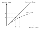
3 is a view for explaining a difference in the degree of wear according to the P / E cycle environment.
4 is a diagram illustrating the effect of the wear ring of a memory cell on the threshold voltage distribution in the program of the memory cell.
5 is a view for explaining a wear level detecting method according to a first embodiment of the present invention.
FIG. 6 is a diagram illustrating an effect of a wear ring of a memory cell on a threshold voltage distribution in erasing the memory cell.
7 is a view for explaining a wear level detecting method according to a second embodiment of the present invention.
8 is a flowchart illustrating a control method of a nonvolatile memory device according to a first embodiment of the present invention.
9 is a flowchart illustrating a control method of a nonvolatile memory device according to a second embodiment of the present invention.
10 is a block diagram illustrating a user device including a solid state disk (hereinafter, referred to as an SSD) according to an embodiment of the present invention.
11 is a block diagram schematically illustrating a memory system according to the present invention.
12 is a block diagram illustrating a data storage device in accordance with another embodiment of the inventive concept.
13 is a schematic diagram of a computing system including a flash memory device.
앞의 일반적인 설명 및 다음의 상세한 설명들은 모두 청구된 발명의 부가적인 설명을 제공하기 위한 예시적인 것이다. 그러므로 본 발명은 여기서 설명되는 실시 예에 한정되지 않고 다른 형태로 구체화될 수도 있다. 여기서 소개되는 실시 예는 개시된 내용이 철저하고 완전해 질 수 있도록 그리고 당업자에게 본 발명의 사상이 충분히 전달될 수 있도록 하기 위해 제공되는 것이다. The foregoing general description and the following detailed description are exemplary and are intended to provide further explanation of the claimed invention. Therefore, the present invention is not limited to the embodiments described herein and may be embodied in other forms. The embodiments disclosed herein are provided so that the disclosure can be thorough and complete, and will fully convey the scope of the invention to those skilled in the art.
본 명세서에서, 어떤 부분이 어떤 구성요소를 포함한다고 언급되는 경우에, 이는 그 외의 다른 구성요소를 더 포함할 수도 있다는 것을 의미한다. 또한, 여기에서 설명되고 예시되는 각 실시 예는 그것의 상보적인 실시 예도 포함한다. 이하, 본 발명의 실시 예를 첨부된 도면을 참조하여 상세하게 설명한다.In this specification, when it is mentioned that a certain element includes an element, it means that it may further include other elements. In addition, each embodiment described and illustrated herein includes its complementary embodiment. DETAILED DESCRIPTION OF THE PREFERRED EMBODIMENTS Hereinafter, embodiments of the present invention will be described in detail with reference to the accompanying drawings.
도 1은 불휘발성 메모리 장치를 보여주는 블록도이다. 도 1을 참조하면, 불휘발성 메모리 장치(10)는 셀 어레이(11), 어드레스 디코더(12), 페이지 버퍼(13), 그리고 제어 로직(14)을 포함한다.1 is a block diagram illustrating a nonvolatile memory device. Referring to FIG. 1, the
셀 어레이(11)는 복수의 메모리 블록(Memory Block)을 포함할 수 있다. 도 1에서는 설명의 편의를 위하여 하나의 메모리 블록을 포함하는 셀 어레이(11)가 도시되어 있다. 메모리 블록들 각각은 복수의 페이지(Pages)로 구성될 수 있다. 그리고 각각의 페이지는 복수의 메모리 셀들로 구성될 수 있다. 불휘발성 메모리 장치(10)에서, 메모리 블록 단위로 소거 동작이 수행되고, 페이지 단위로 쓰기 또는 읽기 동작이 수행될 수 있다. The
셀 어레이(11)는 복수의 메모리 셀들을 포함할 수 있다. 메모리 셀들은 셀 스트링 구조(Cell String Structure)로 되어 있다. 하나의 셀 스트링은 스트링 선택 라인(SSL: String Selection Line)에 연결되는 스트링 선택 트랜지스터(SST), 복수의 워드 라인(WL0~WLn-1)에 연결되는 복수의 메모리 셀들, 그리고 접지 선택 라인(GSL: Ground Selection Line)에 연결되는 접지 선택 트랜지스터(GST)를 포함한다. 스트링 선택 트랜지스터(SST)는 비트 라인(BL)에 연결되고, 접지 선택 트랜지스터(GST)는 공통 소스 라인(CSL: Common Source Line)에 연결된다. The
여기서, 셀 어레이(11)를 구성하는 메모리 셀들은 플로팅 게이트 또는 전하 트랩층과 같은 전하 저장층을 갖는 메모리 셀 또는 가변 저항 소자를 갖는 메모리 셀로 구현될 수 있다. 메모리 셀 어레이(11)는 단층 어레이 구조(single-layer array structure)(또는, 2차원 어레이 구조라고 불림) 또는 다층 어레이 구조(multi-layer array structure)(또는, 수직형 또는 스택형 3차원 어레이 구조라고 불림)를 갖도록 구현될수 있을 것이다.Here, the memory cells constituting the
어드레스 디코더(12)는 선택 라인(SSL, GSL) 또는 워드 라인(WL0~WLn-1)을 통해 셀 어레이(11)와 연결된다. 프로그램 또는 읽기 동작 시에, 어드레스 디코더(12)는 어드레스(Address)를 입력받고, 어느 하나의 워드 라인(예를 들면, WL1)을 선택한다. 한편, 어드레스 디코더(12)는 선택 워드 라인 또는 비선택 워드 라인으로 프로그램 또는 읽기 동작에 필요한 전압을 전달한다.The
페이지 버퍼(13)는 기입 드라이버로서 또는 감지 증폭기로서 동작한다. 페이지 버퍼(13)는 선택된 메모리 셀들에 프로그램될 데이터나, 선택된 메모리 셀들로부터 읽은 데이터를 임시로 저장할 수 있다. 페이지 버퍼(13)는 비트 라인(BL0~BLm-1)을 통해 셀 어레이(11)와 연결된다. 페이지 버퍼(13)는 프로그램 동작 시에는 데이터(Data)를 입력받아 선택된 페이지의 메모리 셀들에 전달한다. 페이지 버퍼(13)는 읽기 동작 시에 선택된 페이지의 메모리 셀들로부터 데이터를 읽고, 외부로 데이터(Data)를 출력한다. The
제어 로직(14)은 외부로부터의 명령어(CMD)나 제어에 따라 불휘발성 메모리 장치(10)의 프로그램, 읽기, 및 소거 등의 동작을 제어할 수 있다. 예를 들면, 프로그램 동작시 제어 로직(14)은 어드레스 디코더(12)를 선택 워드 라인으로 프로그램 전압이 제공되도록 제어할 수 있다. 제어 로직(14)은 페이지 버퍼(13)를 제어함으로 선택된 페이지에 프로그램 데이터가 제공되도록 할 수 있다.The
도 2는 메모리 셀의 일반적인 구조를 설명하기 위한 단면도이다. 도 2를 참조하면 메모리 셀(20)의 반도체 기판(21)에는 불순물이 제 1 불순물 영역(21a) 및 제 2 불순물 영역(21b)이 형성된다. 반도체 기판(21) 중 제 1 및 제 2 불순물 영역(21a, 21b) 사이에 위치한 부분에는 일반적으로 채널 영역이 형성된다. 그리고, 제 1 및 제 2 불순물 영역(21a, 21b)과 접촉하는 반도체 기판(21) 상에는 게이트 구조체가 형성된다. 게이트 구조체는 터널링 산화층(22), 전하 저장층(23), 블로킹 산화층(24) 및 게이트 전극층(25)이 순차적으로 형성된다. 게이트 전극층(25)은 전도성 물질로 이루어진다. 2 is a cross-sectional view illustrating a general structure of a memory cell. Referring to FIG. 2, impurities are formed in the
터널링 산화층(22)은 제 1 및 제 2 불순물 영역(21a, 21b)과 접촉한다. 프로그램 동작에서, 반도체 기판(11)을 통해 이동하는 전하는 터널링 산화층(22)을 통과하여 전하 저장층(23)에 트랩(Trap)된다. 소거 동작에서, 전하 저장층(23)에 트랩된 전하는 F-N 터널링에 의해 반도체 기판(11)으로 방출된다. 전하 저장층(23)에 트랩된 전하의 양은 메모리 셀(20)의 문턱 전압 변화에 영향을 준다. 이러한 문턱 전압 변화의 메카니즘에 의해, 메모리 셀(20)은 데이터를 저장할 수 있다. The tunneling oxide layer 22 is in contact with the first and
한편, 메모리 셀(20)이 프로그램과 소거를 반복함에 따라(P/E 사이클 횟수가 증가함에 따라), 터널링 산화층(22)은 열화되고, 터널링 산화층(22)에 누설 경로가 형성된다. 그 결과, 누설 경로를 통해서 전하 저장층(23)에 저장된 전하가 방출되므로, 메모리 셀(20)의 데이터 유지(Data Retention) 특성은 저하된다. On the other hand, as the memory cell 20 repeats program and erase (as the number of P / E cycles increases), the tunneling oxide layer 22 deteriorates, and a leakage path is formed in the tunneling oxide layer 22. As a result, since the charge stored in the charge storage layer 23 is released through the leakage path, the data retention characteristic of the memory cell 20 is degraded.
이와 같은 P/E 사이클 횟수 증가에 따른 메모리 셀(20)의 성능 저하 및 그에 따른 수명 감소를 최소화하기 위해, 다양한 관리 방법이 사용된다. 예를 들어, 새로운 데이터를 프로그램 할 때 P/E 사이클 횟수가 낮은 메모리 블록에 우선적으로 프로그램할 수 있다. 그러면, 각 메모리 블록들의 P/E 사이클 횟수가 균등하게 관리될 수 있다. 이를 웨어 레벨링(Wear Leveling)이라 한다. Various management methods are used to minimize the performance degradation of the memory cell 20 and the decrease in the lifetime according to the increase in the number of P / E cycles. For example, when programming new data, you may preferentially program memory blocks with low P / E cycles. Then, the number of P / E cycles of each memory block can be managed evenly. This is called wear leveling.
또한, 관리 방법의 다른 예로서, P/E 사이클 횟수가 높은 메모리 블록을 프로그램할 때 ISPP(Incremental Step Pulse Program) 전압을 전압 레벨을 감소시키는 방법이 있다. 이를 통해, 메모리 셀의 문턱 전압 산포를 조밀하게 되고 더 큰 데이터 유지(Data Retention) 마진(Margin)이 확보된다. 이를 능동적 성능 제어(Dynamic Performance Control)이라 한다. As another example of the management method, an incremental step pulse program (ISPP) voltage may be reduced when a memory block having a high number of P / E cycles is programmed. This densifies the threshold voltage distribution of the memory cell and ensures a greater Data Retention Margin. This is called dynamic performance control.
그러나, 이러한 방법들은 통상 P/E 사이클의 횟수만을 참조하여 수행되므로, 메모리 셀의 웨어링 정도(Wearing Degree)를 정확히 반영하지 못하는 문제가 있다.즉, 이러한 관리 방법들은 메모리 셀의 웨어링 정도를 판단하는 기준으로서, P/E 사이클 횟수를 이용한다. 그러나, P/E 사이클 횟수는 메모리 셀의 웨어링 정도를 나타내는데 있어서 일정한 한계를 가진다. However, since these methods are usually performed only by referring to the number of P / E cycles, there is a problem in that they do not accurately reflect the wear degree of the memory cell. That is, these management methods determine the wear level of the memory cell. As a reference, the number of P / E cycles is used. However, the number of P / E cycles has a certain limit in indicating the degree of wear of a memory cell.
1회 P/E 사이클이 수행된 데 따른 메모리 셀의 웨어링 정도는 프로그램 또는 소거할 때의 환경에 의해 달라질 수 있다. 메모리 셀의 웨어링 정도에 영향을 미치는 환경 변수로는 온도 및 P/E 사이클의 동작 기간이 있을 수 있다. The degree of wear of a memory cell according to one P / E cycle is performed may vary depending on the environment at the time of programming or erasing. Environmental variables that affect the degree of wear of a memory cell may include temperature and operating periods of P / E cycles.
예를 들어, 프로그램 또는 소거시의 온도가 고온이면, 메모리 셀의 웨어링 정도는 상온일 때보다 낮아진다. 또한, 동일한 회수의 P/E 사이클이 수행된다 하더라도, 오랜 기간에 걸쳐 수행되는 것(예를 들어, 30일 동안 30회)이 단기간에 걸쳐 수행되는 것(예를 들어, 1일 동안 30회)보다 메모리 셀을 덜 마모(Wearing)시킨다.For example, when the temperature at the time of programming or erasing is high, the degree of wear of the memory cell is lower than at normal temperature. Also, even if the same number of P / E cycles are performed, what is performed over a long period of time (eg, 30 times for 30 days) is performed over a short period of time (eg, 30 times for 1 day). Less wear on memory cells than on
도 3은 P/E 사이클 환경에 따른 웨어링 정도의 차이를 설명하기 위한 도면이다. 도 3을 참조하면, X축은 수행된 P/E 사이클의 횟수를 나타내고, Y축은 메모리 셀의 웨어링 인덱스(Wearing Index)를 나타낸다. 여기서 웨어링 인덱스는 메모리 셀의 웨어링 정도를 수치화한 값이다. 참조 곡선(Reference Curve)은 P/E 사이클 횟수만을 고려하여 웨어링 인덱스를 표시한 곡선이다. 실제 곡선(Real Curve)은 실제 메모리 셀의 웨어링 인덱스를 표시한 곡선으로서, 상대적으로 고온 및 장기간의 P/E 사이클 환경을 갖는다.3 is a view for explaining a difference in the degree of wear according to the P / E cycle environment. Referring to FIG. 3, the X axis represents the number of P / E cycles performed, and the Y axis represents a wearing index of the memory cell. Here, the wear ring index is a value obtained by quantifying the wear degree of the memory cell. A reference curve is a curve indicating a wear ring index considering only the number of P / E cycles. The real curve is a curve representing the wear ring index of the real memory cell, and has a relatively high temperature and a long P / E cycle environment.
실제 곡선과 참조 곡선을 비교하여 설명하면, P/E 사이클의 횟수가 N회 일 때, 참조 곡선에 따른 웨어링 인덱스는 A가 된다. 동일한 P/E 사이클 횟수에 대해 실제 곡선에 따른 웨어링 인덱스는 A'가 된다. 즉, 참고 곡선에 따른 웨어링 인덱스와 실제 메모리 셀의 웨어링 인덱스 사이에는 A-A'의 오차가 존재한다. 따라서, 참조 곡선에 따를 때 메모리 셀은 실제 웨어링 인덱스보다 더 큰 웨어링 인덱스를 갖는 것으로 간주된다.When comparing the actual curve with the reference curve, when the number of P / E cycles is N, the wear index according to the reference curve becomes A. For the same number of P / E cycles, the wear ring index according to the actual curve is A '. That is, an error of A-A 'exists between the wear ring index according to the reference curve and the wear ring index of the actual memory cell. Thus, according to the reference curve, the memory cell is considered to have a larger wear ring index than the actual wear ring index.
한편, 참조곡선에 있어서, 웨어링 인덱스 A 및 A'는 P/E 사이클 횟수는 N 및 N'과 각각 대응한다. 따라서, A-A' 크기의 웨어링 인덱스 오차는 N-N'회의 P/E 사이클 오차와 동일하다. 이러한 경우, 메모리 장치의 기능 유지를 위한 관리 동작(즉, 웨어 레벨링 동작 또는 능동적 성능 제어 동작)이 최적으로 수행되지 못하는 비효율이 발생할 수 있다. 따라서, 실제 웨어링 정도(또는, 웨어링 인덱스)와의 오차를 최소화하는 웨어링 정도 검출 방법이 필요하다.On the other hand, in the reference curve, the wear ring indexes A and A 'correspond to N and N' of the number of P / E cycles, respectively. Therefore, the wearing index error of A-A 'size is equal to the P / E cycle error of N-N' times. In this case, an inefficiency may occur in which a management operation (ie, a wear leveling operation or an active performance control operation) for maintaining the function of the memory device is not optimally performed. Accordingly, there is a need for a wear degree detecting method for minimizing an error with an actual wear degree (or wear ring index).
도 4 내지 도 7은 본 발명에 따른 불휘발성 메모리 장치의 제어 방법을 설명하기 위한 도면이다. 구체적으로, 도 4 내지 도 7에서는 메모리 셀의 웨어링 정도를 검출하는 방법이 제공된다. 4 to 7 are diagrams for describing a method of controlling a nonvolatile memory device according to the present invention. Specifically, FIGS. 4 to 7 provide a method of detecting a wear level of a memory cell.
도 4는 메모리 셀의 프로그램에 있어서, 메모리 셀의 웨어링이 문턱 전압 분포에 미치는 영향을 나타내는 도면이다. 도 4를 참조하면, 초기 문턱 전압 분포(410)는 소거된 메모리 셀들의 문턱 전압 분포를 나타낸다. 낮은 문턱 전압 분포(420)는 웨어링 정도가 낮은 메모리 셀들을 프로그램한 문턱 전압 분포를 나타낸다. 높은 문턱 전압 분포(430)는 웨어링 정도가 높은 메모리 셀들을 프로그램한 문턱 전압 분포를 나타낸다. 4 is a diagram illustrating the effect of the wear ring of a memory cell on the threshold voltage distribution in the program of the memory cell. Referring to FIG. 4, an initial
메모리 셀의 웨어링 정도가 증가하면(즉, P/E 사이클이 증가하면), 메모리 셀의 프로그램 속도도 증가한다. 이는 P/E 사이클의 반복에 의해 터널링 산화층(22, 도 2 참조)이 열화되기 때문이다. 또한, 터널링 산화층(22)의 열화에 따라, 동일한 프로그램 전압에 의해 메모리 셀의 문턱 전압이 증가되는 폭도 증가한다. 예를 들어, 웨어링 정도가 낮은 메모리 셀들은 프로그램 전압을 인가하면, 초기 문턱 전압 분포(410)에서 낮은 문턱 전압 분포(420)로 문턱 전압 분포가 변화한다. 반면에, 웨어링 정도가 높은 메모리 셀들은 프로그램 전압을 인가하면, 초기 문턱 전압 분포(410)에서 높은 문턱 전압 분포(430)로 문턱 전압 분포가 변화한다. As the degree of wear of a memory cell increases (ie, P / E cycles increase), the program speed of the memory cell also increases. This is because the tunneling oxide layer 22 (see Fig. 2) is deteriorated by repetition of the P / E cycle. In addition, as the tunneling oxide layer 22 deteriorates, the width at which the threshold voltage of the memory cell is increased by the same program voltage also increases. For example, when the memory cells having a low wear level apply a program voltage, the threshold voltage distribution is changed from the initial
따라서, 웨어링 정도가 높은 메모리 셀들을 프로그램한 문턱 전압 분포(430)는 웨어링 정도가 낮은 메모리 셀들을 프로그램한 문턱 전압 분포(420) 보다 X축의 양의 방향으로 더 치우쳐진다. 그리고, 웨어링 정도가 낮은 셀들의 최대 문턱 전압(Vupper)은 웨어링 정도가 높은 셀들의 최대 문턱 전압(V'upper)보다 낮다.Therefore, the
도 5는 본 발명의 제 1 실시 예에 따른 웨어링 정도 검출 방법을 설명하기 위한 도면이다. 본 발명의 제 1 실시 예는 메모리 셀의 프로그램을 이용하여 실시된다. 도 5를 참조하면, 초기 문턱 전압 분포(510)는 소거된 메모리 셀들의 문턱 전압 분포를 나타낸다. 제 1 문턱 전압 분포(520)는 제 1 메모리 셀들을 프로그램한 문턱 전압 분포를 나타낸다. 제 2 문턱 전압 분포(530)는 제 2 메모리 셀들을 프로그램한 문턱 전압 분포를 나타낸다. 제 3 문턱 전압 분포(540)는 제 3 메모리 셀들을 프로그램한 문턱 전압 분포를 나타낸다. 5 is a view for explaining a wear level detecting method according to a first embodiment of the present invention. A first embodiment of the present invention is implemented using a program of a memory cell. Referring to FIG. 5, an initial
본 실시 예에서, 제 1 메모리 셀들의 웨어링 정도는 제 2 메모리 셀들의 웨어링 정도보다 낮다. 그리고, 제 2 메모리 셀들의 웨어링 정도는 제 3 메모리 셀들의 웨어링 정도보다 낮다. 앞서 설명한 바와 같이, 동일한 프로그램 전압에 의한 문턱 전압의 증가폭은 메모리 셀의 웨어링 정도가 클수록 증가한다. 따라서, 소거 상태에 있는 메모리 셀들을 동일한 프로그램 전압에 의해 프로그램하면, 웨어링 정도가 높은 메모리 셀들은 높은 문턱 전압을 갖는다. 그리고, 웨어링 정도가 낮은 메모리 셀들은 낮은 문턱 전압을 갖는다.In this embodiment, the wear degree of the first memory cells is lower than the wear degree of the second memory cells. The wear degree of the second memory cells is lower than that of the third memory cells. As described above, the increase of the threshold voltage by the same program voltage increases as the wear rate of the memory cell increases. Therefore, when memory cells in the erased state are programmed by the same program voltage, memory cells having a high degree of wear have high threshold voltages. In addition, memory cells having a low degree of wear have low threshold voltages.
메모리 셀들의 웨어링 정도를 검출하기 위해서 제 1, 제 2 및 제 3 메모리 셀들을 동일한 프로그램 전압으로 프로그램한다. 그에 따라, 제 1, 제 2 및 제 3 메모리 셀들의 문턱 전압 분포는 초기 문턱 전압 분포(510)에서 제 1, 제 2 및 제 3 문턱 전압 분포(520, 530, 540)로 각각 상승한다. 제 1, 제 2 및 제 3 메모리 셀들의 웨어링 정도를 검출하기 위하여, 각 메모리 셀들의 최대 문턱 전압을 검출한다. 최대 문턱 전압은 프로그램된 각 메모리 셀들에 대한 읽기(Read) 동작을 통해 검출된다. The first, second and third memory cells are programmed with the same program voltage to detect the degree of wear of the memory cells. Accordingly, the threshold voltage distributions of the first, second and third memory cells rise from the initial
실시 예로서, 전압 레벨을 일정하게 증가시킨 복수의 읽기 전압들(V1, V2, V3, V4)에 의해 읽기 동작이 수행될 수 있다. 각 읽기 전압에 대해서 메모리 셀들이 모두 턴 온되는 경우, 메모리 셀들에는 읽기 전압에 대응되는 웨어링 인덱스가 할당된다. 웨어링 인덱스는 각 메모리 셀들의 웨어링 정도를 수치화한 지표로서 정의된다.According to an embodiment, a read operation may be performed by the plurality of read voltages V1, V2, V3, and V4 that increase the voltage level constantly. When all of the memory cells are turned on for each read voltage, a wear ring index corresponding to the read voltage is allocated to the memory cells. The wear index is defined as an index indicating a wear degree of each memory cell.
읽기 전압(V1)에 대해서, 제 1 메모리 셀들은 모두 턴 온된다. 따라서, 제 1 메모리 셀들에는 제 1 웨어링 인덱스가 할당한다. 제 2 및 제 3 메모리 셀들은 턴 온되지 않은 메모리 셀들을 포함한다. 따라서, 읽기 전압(V1)에 대해서, 제 2 및 제 3 메모리 셀들은 웨어링 인덱스가 할당되지 않는다.For the read voltage V1, all of the first memory cells are turned on. Accordingly, the first wear ring index is allocated to the first memory cells. The second and third memory cells include memory cells that are not turned on. Thus, for the read voltage V1, the second and third memory cells are not assigned a wear index.
웨어링 인덱스가 할당되지 않은 제 2 및 제 3 메모리 셀들에 대해서는, 읽기 전압(V2)에 의한 읽기 동작이 수행된다. 읽기 전압(V2)에 대해서, 제 2 메모리 셀들은 모두 턴 온된다. 따라서, 제 2 메모리 셀들에는 제 2 웨어링 인덱스가 할당된다. 제 3 메모리 셀들은 턴 온되지 않은 메모리 셀들을 포함한다. 따라서, 제 3 메모리 셀들에는 웨어링 인덱스가 할당되지 않고, 증가된 읽기 전압에 의한 읽기 동작이 수행된다.For the second and third memory cells to which the wear ring index is not allocated, a read operation by the read voltage V2 is performed. For the read voltage V2, the second memory cells are all turned on. Thus, a second wear index is allocated to the second memory cells. The third memory cells include memory cells that are not turned on. Accordingly, a wear ring index is not allocated to the third memory cells, and a read operation is performed by an increased read voltage.
읽기 전압(V3)에 대해서, 제 3 메모리 셀들은 턴 온되지 않은 메모리 셀들을 포함한다. 따라서, 제 3 메모리 셀들에는 웨어링 인덱스가 할당되지 않고, 다시 증가된 읽기 전압에 의한 읽기 동작이 수행된다.For the read voltage V3, the third memory cells include memory cells that are not turned on. Accordingly, a wear ring index is not allocated to the third memory cells, and a read operation is performed by the increased read voltage.
읽기 전압(V4)에 대해서, 제 3 메모리 셀들은 모두 턴 온된다. 따라서, 제 3 메모리 셀들에는 제 3 웨어링 인덱스가 할당된다. For the read voltage V4, all of the third memory cells are turned on. Thus, a third wear index is allocated to the third memory cells.
각 웨어링 인덱스들은 메모리 셀의 웨어링 정도를 수치화한 값으로서, 낮은 읽기 전압에 의해 할당된 웨어링 인덱스일수록 낮은 웨어링 정도를 나타낸다. 예를 들어, 읽기 전압들(V1, V2, V3, V4)에 대응하는 웨어링 인덱스들을 각각 1, 2, 3, 4라고 정의한다. 그에 따르면, 제 1, 제 2 및 제 3 메모리 셀들의 웨어링 인덱스는 각각 1, 2, 4가 된다. 제 2 메모리 셀들은 제 1 메모리 셀들 보다 웨어링 정도가 1 높다. 제 3 메모리 셀들은 제 1 및 제 2 메모리 셀들보다 웨어링 정도가 각각 3 및 2 높다.Each wear ring index is a numerical value of the wear rate of a memory cell. The wear ring index assigned by a low read voltage indicates a lower wear rate. For example, the wear indexes corresponding to the read voltages V1, V2, V3, and V4 are defined as 1, 2, 3, and 4, respectively. According to him, the wear indexes of the first, second and third memory cells are 1, 2, and 4, respectively. The second memory cells have a wear degree higher than that of the first memory cells. The third memory cells have a wear degree higher than that of the first and second memory cells by 3 and 2, respectively.
위와 같이 본 발명에서 웨어링 인덱스는 프로그램 전압에 의해 변화되는 문턱 전압의 크기를 이용하여 검출된다. 따라서, 웨어링 인덱스는 터널링 산화층(22, 도 2 참조)의 실제 열화정도를 정확하게 반영할 수 있다. 즉, P/E 사이클 환경(예를 들어, 온도 또는 P/E 사이클 동작 기간)까지 고려된다. 그 결과, P/E 사이클 횟수만을 참조하는 방법보다 정확한 웨어링 정도의 검출이 가능하다.As described above, in the present invention, the wear ring index is detected using the magnitude of the threshold voltage which is changed by the program voltage. Accordingly, the wear ring index may accurately reflect the degree of actual deterioration of the tunneling oxide layer 22 (see FIG. 2). That is, up to P / E cycle environment (eg, temperature or P / E cycle operating period) is considered. As a result, more accurate wear ring detection is possible than the method of referring only to the number of P / E cycles.
도 6은 메모리 셀의 소거에 있어서, 메모리 셀의 웨어링이 문턱 전압 분포에 미치는 영향을 나타내는 도면이다. 도 6을 참조하면, 문턱 전압 분포(610)는 프로그램된 메모리 셀들의 문턱 전압 분포를 나타낸다. 문턱 전압 분포(620)는 웨어링 정도가 낮은 메모리 셀들을 소거한 문턱 전압 분포를 나타낸다. 소거 전압 분포(630)는 웨어링 정도가 높은 메모리 셀들을 소거한 문턱 전압 분포를 나타낸다. FIG. 6 is a diagram illustrating an effect of a wear ring of a memory cell on a threshold voltage distribution in erasing the memory cell. Referring to FIG. 6, the
메모리 셀의 웨어링 정도가 증가할수록(즉, P/E 사이클이 증가할수록), 터널링 산화층(22, 도 2 참조)에 트랩되는 전자수는 증가한다. 그리고, 터널링 산화층(22)에 트랩된 전자가 많을수록, F-N 터널링(Fowler-Nordheim Tunneling)을 방해하는 힘이 강해진다. 그 결과, 메모리 셀의 웨어링 정도가 증가할수록, 메모리 셀의 소거 속도는 감소한다. 그리고, 동일한 소거 전압으로 메모리 셀을 소거할 경우, 웨어링 정도가 큰 메모리 셀 일수록 문턱 전압의 변화가 작다.As the degree of wear of the memory cell increases (ie, as the P / E cycle increases), the number of electrons trapped in the tunneling oxide layer 22 (see FIG. 2) increases. In addition, the more electrons trapped in the tunneling oxide layer 22, the stronger the interference of F-N tunneling (Fowler-Nordheim Tunneling). As a result, as the wear degree of the memory cell increases, the erase speed of the memory cell decreases. When the memory cell is erased with the same erase voltage, the change in the threshold voltage is smaller for the memory cell having a greater degree of wear ring.
예를 들어, 같은 문턱 전압 분포(610)를 갖도록 프로그램된 메모리 셀들에 소거 동작을 수행하면, 웨어링 정도가 높은 메모리 셀들의 문턱 전압 변화폭은 웨어링 정도가 낮은 메모리 셀의 변화폭보다 작다. 따라서, 웨어링 정도가 높은 메모리 셀들을 소거한 문턱 전압 분포(630)는 웨어링 정도가 낮은 메모리 셀들을 소거한 문턱 전압 분포(620) 보다 X축의 양의 방향으로 더 치우쳐진다. For example, when an erase operation is performed on memory cells programmed to have the same
그러므로 실시 예로서, 제 1 실시 예와 유사하게, 소거된 메모리 셀들의 최대 문턱 전압을 읽음으로써, 웨어링 인덱스를 검출할 수 있다. 즉, 전압 레벨을 일정하게 증가시킨 복수의 읽기 전압들로써 소거된 메모리 셀들을 읽는다. 읽기 전압에 대해서 메모리 셀들이 모두 턴 온되는 경우, 메모리 셀들에는 읽기 전압에 대응되는 웨어링 인덱스가 할당된다. 읽기 전압에 대해 턴 온되지 않은 메모리 셀이 존재하면, 증가된 읽기 전압으로서 해당 메모리 셀들에 대해 다시 읽기 동작을 수행한다. 이때, 구체적인 웨어링 인덱스 검출 방법은 제 1 실시 예에서 설명한 바와 동일하다. Therefore, as an embodiment, similar to the first embodiment, the wear ring index may be detected by reading the maximum threshold voltages of the erased memory cells. That is, the erased memory cells are read with a plurality of read voltages with a constant increase in voltage level. When the memory cells are all turned on with respect to the read voltage, the wear ring index corresponding to the read voltage is allocated to the memory cells. If a memory cell is not turned on with respect to the read voltage, the read operation is performed again with respect to the memory cells as the increased read voltage. At this time, the specific wear ring index detection method is the same as described in the first embodiment.
도 7은 본 발명의 제 2 실시 예에 따른 웨어링 정도 검출 방법을 설명하기 위한 도면이다. 본 발명의 제 2 실시 예는 메모리 셀의 소거를 이용하여 실시된다. 도 7을 참조하면, 초기 전압 분포(710)는 프로그램된 메모리 셀들의 문턱 전압 분포를 나타낸다. 본 실시 예에서, 소거 동작은 점증적으로 증가되는 소거 전압을 사용하여 수행된다(ISPE : Incremental Step Pulse Erase). 7 is a view for explaining a wear level detecting method according to a second embodiment of the present invention. A second embodiment of the present invention is implemented using the erase of memory cells. Referring to FIG. 7, an
앞서 설명한 바와 같이, 메모리 셀들의 웨어링 정도에 따라 메모리 셀들을 소거한 문턱 전압 분포는 달라진다. 따라서, 점증적 펄스 소거(ISPE)에 의해 메모리 셀들을 소거하는 경우, 소거 동작이 수행된 횟수에 의해 메모리 셀들의 웨어링 인덱스가 검출될 수 있다. As described above, the threshold voltage distribution of erasing the memory cells varies according to the degree of wear of the memory cells. Therefore, when erasing memory cells by incremental pulse erasure (ISPE), the wear index of the memory cells may be detected by the number of times the erase operation is performed.
예를 들어, 도 7을 참조하면, 가장 왼쪽의 문턱 전압 분포(N=3, 실선)는 완전한 소거 상태의 문턱 전압 분포를 나타낸다. 본 실시 예에서는 프로그램된 메모리 셀들을 1단계 소거 전압으로써 소거한다(제 1단계 소거). 소거된 메모리 셀의 문턱 전압 분포는 초기 전압 분포(710)에서 1단계 문턱 전압 분포(N=1)으로 변화한다. 1단계 문턱 전압 분포(N=1)는 완전한 소거 상태의 문턱 전압 분포가 아니다. For example, referring to FIG. 7, the leftmost threshold voltage distribution N = 3 (solid line) represents the threshold voltage distribution in a completely erased state. In the present exemplary embodiment, the programmed memory cells are erased using the first stage erase voltage (first stage erase). The threshold voltage distribution of the erased memory cell changes from the
따라서, 1단계 소거 전압보다 증가한 2단계 소거 전압으로써 메모리 셀들을 다시 소거한다(제 2단계 소거). 제 2단계 소거에 의해, 메모리 셀들의 문턱 전압 분포는 1단계 문턱 전압 분포(N=1)에서 2단계 문턱 전압 분포(N=2)로 변화한다. 2단계 문턱 전압 분포(N=2)도 완전한 소거 상태의 문턱 전압 분포가 아니다.Accordingly, the memory cells are erased again by using the two-step erase voltage that is increased from the one-step erase voltage (second erase). By the second stage erase, the threshold voltage distribution of the memory cells is changed from the first stage threshold voltage distribution N = 1 to the second stage threshold voltage distribution N = 2. The two-stage threshold voltage distribution (N = 2) is also not a threshold voltage distribution in a completely erased state.
그러므로, 2단계 소거 전압보다 증가한 3단계 소거 전압으로써 메모리 셀들을 다시 소거한다(제 3단계 소거). 제 3단계 소거에 의해, 메모리 셀들의 문턱 전압 분포는 2단계 문턱 전압 분포(N=2)에서 3단계 문턱 전압 분포(N=3)로 변화한다. 3단계 문턱 전압 분포(N=3)는 완전한 소거 상태의 문턱 전압 분포이다. 따라서, 소거 동작은 종료되고, 수행된 소거 동작의 횟수(즉, 3)는 메모리 셀들의 웨어링 인덱스로서 검출된다.Therefore, the memory cells are again erased (third stage erase) with the third stage erase voltage increased from the second stage erase voltage. By the third stage erase, the threshold voltage distribution of the memory cells is changed from the second stage threshold voltage distribution N = 2 to the three stage threshold voltage distribution N = 3. The three-stage threshold voltage distribution (N = 3) is a threshold voltage distribution in a completely erased state. Thus, the erase operation is terminated, and the number of erase operations (ie, 3) performed is detected as the wear index of the memory cells.
마찬가지로, 어떠한 메모리 셀들이 2번의 소거 동작에 의해 완전한 소거 상태의 문턱 전압 분포를 갖는다면, 메모리 셀들의 웨어링 인덱스는 2가 된다. 메모리 셀들의 웨어링 정도가 클수록 동일한 소거 전압에 의한 문턱 전압 변화는 작아진다. 따라서, 메모리 셀들의 웨어링 정도가 클수록, 웨어링 인덱스도 증가할 것이다. Similarly, if any memory cells have a threshold voltage distribution of a complete erase state by two erase operations, the wear index of the memory cells becomes two. The greater the degree of wear of the memory cells, the smaller the change in the threshold voltage due to the same erase voltage. Therefore, as the degree of wear of memory cells increases, the wear ring index will increase.
한편, 본 실시 예에서, 반복되는 소거 동작마다 증가시키는 소거 전압의 크기는 웨어링 인덱스의 정확도에 따라 다르게 설정될 수 있다. 증가시키는 소거 전압의 크기가 작아질수록, 웨어링 인덱스의 정확도는 증가할 것이다.Meanwhile, in the present embodiment, the magnitude of the erase voltage that is increased for each repeated erase operation may be set differently according to the accuracy of the wear index. As the magnitude of the increasing erase voltage decreases, the accuracy of the wear ring index will increase.
이와 같이, 제 2 실시 예에 따르면, 소거된 메모리 셀의 문턱 전압 분포로부터 웨어링 인덱스를 검출할 수 있다. 따라서, 웨어링 인덱스는 터널링 산화층(22, 도 2 참조)의 실제 열화정도를 정확하게 반영할 수 있다. 즉, P/E 사이클 환경(예를 들어, 온도 또는 P/E 사이클 동작 기간)까지 고려된다. 그 결과, P/E 사이클 횟수만을 참조하는 방법보다 정확한 웨어링 정도의 검출이 가능하다.As described above, according to the second exemplary embodiment, the wear ring index may be detected from the threshold voltage distribution of the erased memory cell. Accordingly, the wear ring index may accurately reflect the degree of actual deterioration of the tunneling oxide layer 22 (see FIG. 2). That is, up to P / E cycle environment (eg, temperature or P / E cycle operating period) is considered. As a result, more accurate wear ring detection is possible than the method of referring only to the number of P / E cycles.
도 8은 본 발명의 제 1 실시 예에 따른 불휘발성 메모리 장치의 제어 방법을 나타내는 순서도이다. 도 8을 참조하면, 불휘발성 메모리 장치의 제어 방법은 S810 단계 내지 S840 단계를 포함한다.8 is a flowchart illustrating a control method of a nonvolatile memory device according to a first embodiment of the present invention. Referring to FIG. 8, a method of controlling a nonvolatile memory device may include steps S810 to S840.
S810 단계에서, 웨어링 인덱스를 검출할 메모리 셀들을 프로그램한다. 웨어링 인덱스는 메모리 셀의 웨어링 정도를 수치화한 지표이다. 메모리 셀들의 프로그램은 소정의 프로그램 전압을 인가하여 수행된다. 메모리 셀의 프로그램하는 구체적인 방법은 당해 기술 분야에서 널리 알려져 있으므로, 그에 대한 설명은 생략한다.In operation S810, memory cells for detecting a wear index are programmed. The wear ring index is an index indicating a wear degree of a memory cell. The program of the memory cells is performed by applying a predetermined program voltage. Since a specific method of programming a memory cell is well known in the art, a description thereof will be omitted.
S820 단계에서, 프로그램된 메모리 셀들의 문턱 전압을 읽는다. 이때, 각 메모리 셀들의 최대 문턱 전압을 검출하기 위해, 모든 메모리 셀들이 턴 온되는 최소의 읽기 전압을 인가한다. 한편, 읽기 전압을 인가하여 메모리 셀을 읽는 구체적인 방법은 당해 기술 분야에서 널리 알려져 있으므로, 그에 대한 설명은 생략한다.In operation S820, threshold voltages of programmed memory cells are read. In this case, in order to detect the maximum threshold voltage of each memory cell, a minimum read voltage at which all memory cells are turned on is applied. Meanwhile, since a specific method of reading a memory cell by applying a read voltage is well known in the art, a description thereof will be omitted.
구체적으로, 제 1 읽기 전압으로써 읽기 동작을 수행한다. 제 1 읽기 전압이 메모리 셀들의 최대 문턱 전압보다 크면, 제 1 읽기 전압은 모든 메모리 셀들을 턴 온시킨다. 따라서, 제 1 읽기 전압에 대응하는 제 1 웨어링 인덱스를 메모리 셀들의 웨어링 인덱스로서 설정한다. Specifically, a read operation is performed with the first read voltage. If the first read voltage is greater than the maximum threshold voltage of the memory cells, the first read voltage turns on all the memory cells. Therefore, the first wear ring index corresponding to the first read voltage is set as the wear ring index of the memory cells.
한편, 제 1 읽기 전압이 최대 문턱 전압보다 작으면, 제 1 읽기 전압은 일부 메모리 셀들을 턴 온시키지 못한다. 따라서, 제 1 읽기 전압보다 증가한 제 2 읽기 전압으로써 읽기 동작을 다시 수행한다. 제 2 읽기 전압이 메모리 셀들의 최대 문턱 전압보다 크면, 제 2 읽기 전압은 모든 메모리 셀들을 턴 온시킨다. 따라서, 제 2 읽기 전압에 대응하는 제 2 웨어링 인덱스를 메모리 셀들의 웨어링 인덱스로서 설정한다.On the other hand, if the first read voltage is less than the maximum threshold voltage, the first read voltage does not turn on some memory cells. Therefore, the read operation is performed again with the second read voltage increased from the first read voltage. If the second read voltage is greater than the maximum threshold voltage of the memory cells, the second read voltage turns on all the memory cells. Therefore, the second wear ring index corresponding to the second read voltage is set as the wear ring index of the memory cells.
한편, 제 2 읽기 전압이 최대 문턱 전압보다 작으면, 제 2 읽기 전압은 일부 메모리 셀들을 턴 온시키지 못한다. 따라서, 제 2 읽기 전압보다 증가한 제 3 읽기 전압으로써 읽기 동작을 다시 수행한다. 제 3 읽기 전압이 메모리 셀들의 최대 문턱 전압보다 크면, 제 3 읽기 전압은 모든 메모리 셀들을 턴 온시킨다. 따라서, 제 3 읽기 전압에 대응하는 제 3 웨어링 인덱스를 메모리 셀들의 웨어링 인덱스로서 설정한다. On the other hand, if the second read voltage is less than the maximum threshold voltage, the second read voltage does not turn on some memory cells. Therefore, the read operation is performed again with the third read voltage increased from the second read voltage. If the third read voltage is greater than the maximum threshold voltage of the memory cells, the third read voltage turns on all the memory cells. Therefore, the third wear ring index corresponding to the third read voltage is set as the wear ring index of the memory cells.
이와 같이, 모든 메모리 셀이 턴 온될 때까지, 읽기 전압을 점증시키며 읽기 동작을 수행한다. 그리고, 모든 메모리 셀이 턴 온되면, 그 때의 읽기 전압에 대응되는 웨어링 인덱스를 메모리 셀의 웨어링 인덱스로 설정한다.As such, the read operation is performed while increasing the read voltage until all the memory cells are turned on. When all memory cells are turned on, the wear ring index corresponding to the read voltage at that time is set as the wear ring index of the memory cell.
S830 단계에서, 메모리 셀들의 웨어링 인덱스를 검출한다. 웨어링 정도가 높은 메모리 셀일 수록 프로그램 전압에 의한 문턱 전압 변화가 크므로, 메모리 셀을 턴 온시키기 위한 읽기 전압도 높아진다. 한편, S820 단계에서, 높은 읽기 전압에는 높은 웨어링 인덱스가 대응된다. 따라서, 웨어링 정도가 높은 메모리 셀일 수록 높은 웨어링 인덱스가 검출될 것이다.In operation S830, the wear index of the memory cells is detected. Since the memory cell with a higher degree of wear has a larger threshold voltage change due to the program voltage, the read voltage for turning on the memory cell also increases. In operation S820, a high wear ring index corresponds to the high read voltage. Therefore, the higher the wear ring index will be detected in a memory cell having a higher wear ring degree.
S840 단계에서, 웨어링 인덱스를 참조하여, 불휘발성 메모리 장치를 관리하는 프로세스를 수행한다. 이때, 관리 프로세스는 P/E 사이클 증가에 따른 메모리 장치의 성능 및 수명 감소를 개선하기 위한 일반적인 관리 프로세스들을 포함한다.In operation S840, the process of managing the nonvolatile memory device is performed by referring to the wear ring index. At this time, the management process includes general management processes for improving the performance and life reduction of the memory device as the P / E cycle increases.
실시 예로서, 관리 프로세스는 웨어 레벨링(Wear Leveling)일 수 있다. 웨어 레벨링은 새로운 쓰기 데이터가 입력된 경우, 웨어링 인덱스가 낮은 메모리 셀(즉, 웨어링 정도가 낮은 메모리 셀)에 우선적으로 쓰기 데이터를 기록하는 메모리 관리 방법이다. 즉, 웨어 레벨링을 통해, 웨어링 인덱스가 높은 메모리 셀은 더 적게 쓰여지고, 웨어링 인덱스가 낮은 메모리 셀은 더 많이 쓰여진다. 따라서, 전체적인 메모리 셀들의 웨어링 인덱스가 비교적 균등하게 유지될 수 있다.In an embodiment, the management process may be wear leveling. Wear leveling is a memory management method in which write data is preferentially written to memory cells having a low wear ring index (that is, memory cells having a low wear degree) when new write data is input. That is, through wear leveling, less memory cells with a higher wear index are written and more memory cells with a lower wear index are used. Thus, the wear index of the entire memory cells can be maintained relatively evenly.
한편, 실시 예로서, 관리 프로세스는 능동적 성능 제어(Dynamic Performance Control)일 수 있다. 메모리 셀의 웨어링 인덱스가 증가할수록(즉, 메모리 셀의 웨어링 정도가 증가할수록) 데이터 유지 성능(Data Retention Performance)는 저하된다. 따라서, 프로그램되는 메모리 셀의 웨어링 인덱스가 높을수록, 점증적 펄스 프로그램(ISPP : Incremental Step Pulse Program) 전압의 크기를 감소시킨다. 그럼으로써, 프로그램된 메모리 셀의 문턱 전압 분포가 좁아지고, 데이터 유지를 위한 마진이 더 크게 확보된다. 이러한 메모리 제어 방법을 능동적 성능 제어라 한다. Meanwhile, as an embodiment, the management process may be dynamic performance control. As the wear ring index of the memory cell increases (that is, the wear degree of the memory cell increases), the data retention performance decreases. Therefore, the higher the wear ring index of the memory cell being programmed, the smaller the incremental pulse program (ISPP) voltage. As a result, the threshold voltage distribution of the programmed memory cell is narrowed, and a larger margin for data retention is secured. This memory control method is called active performance control.
한편, 도 8에서는 메모리 셀의 프로그램을 이용하여 웨어링 인덱스를 검출하는 방법에 대해 설명하였다. 그러나, 동일한 내용의 검출 방법이 메모리 셀의 소거를 이용하여 수행될 수 있다. 메모리 셀의 소거를 이용하여 웨어링 인덱스를 검출하는 방법은 앞서 도 6의 설명에서 설명된 바와 동일하다.8 illustrates a method of detecting a wear index by using a program of a memory cell. However, the same detection method can be performed using erasing of memory cells. The method of detecting the wear index by erasing the memory cell is the same as described above with reference to FIG. 6.
본 발명의 실시 예에 따르면, 메모리 셀의 웨어링 정도를 보다 정확하게 검출하는 수단이 제공된다. 따라서, 불휘발성 메모리 장치의 성능 및 수명을 개선하기 위한 제어 방법들의 성능이 향상될 수 있다.According to an embodiment of the present invention, a means for more accurately detecting a wear level of a memory cell is provided. Thus, the performance of control methods for improving the performance and lifespan of the nonvolatile memory device can be improved.
도 9는 본 발명의 제 2 실시 예에 따른 불휘발성 메모리 장치의 제어 방법을 나타내는 순서도이다. 도 9를 참조하면, 불휘발성 메모리 장치의 제어 방법은 S910 단계 내지 S970 단계를 포함한다.9 is a flowchart illustrating a control method of a nonvolatile memory device according to a second embodiment of the present invention. 9, a method of controlling a nonvolatile memory device includes steps S910 to S970.
S910 단계에서, 소거 전압을 인가하여 웨어링 인덱스를 검출할 메모리 셀들을 소거한다. 웨어링 인덱스는 메모리 셀의 웨어링 정도를 수치화한 지표이다. 메모리 셀들을 소거 방법은 당해 기술 분야에서 널리 알려져 있으므로, 그에 대한 설명은 생략한다. In operation S910, an erase voltage is applied to erase memory cells for detecting a wear index. The wear ring index is an index indicating a wear degree of a memory cell. Since the method of erasing the memory cells is well known in the art, a description thereof will be omitted.
S920 단계 내지 S930 단계에서, 메모리 셀들의 소거 여부를 검증한다. 메모리 셀들 중 일부가 소거 패스되지 않았으면, 재소거를 위해 S940 단계 내지 S950 단계로 진행한다. 메모리 셀들이 모두 소거 패스되었으면, 웨어링 인덱스를 검출하기 위해 S960 단계로 진행한다. 메모리 셀의 소거 검증 방법은 당해 기술 분야에서 널리 알려져 있으므로, 그에 대한 구체적인 설명은 생략한다.In step S920 to step S930, whether the memory cells are erased is verified. If some of the memory cells have not been erased, the process proceeds to step S940 to step S950 for re-erasing. If all the memory cells have been erased and passed, the process proceeds to step S960 to detect the wear index. Since the erase verification method of the memory cell is widely known in the art, a detailed description thereof will be omitted.
S940 단계 내지 S950 단계에서, 메모리 셀의 일부가 소거 패스 되지 않았으므로, 웨어링 인덱스의 값을 1 증가 시킨다(S940). 실시 예로서, 초기 웨어링 인덱스의 값은 1일 수 있다. 그리고, 메모리 셀의 재소거를 위해 소거 전압을 증가시킨다(S950). 그리고, 증가된 소거 전압으로써 메모리 셀을 재소거하기 위해, S910단계로 진행한다. S940 단계 내지 S950 단계를 통해, 메모리 셀의 소거가 페일될 때마다, 웨어링 인덱스 및 소거 전압을 증가시킨다. 따라서, 소거 동작이 반복될 수록 메모리 셀의 웨어링 인덱스는 지속적으로 증가한다.In steps S940 to S950, since a part of the memory cells is not erased, the value of the wear ring index is increased by one (S940). In an embodiment, the value of the initial wear index may be 1. In addition, the erase voltage is increased to erase the memory cell (S950). In order to erase the memory cell with the increased erase voltage, the process proceeds to step S910. In operation S940 to operation S950, whenever the erase of the memory cell is failed, the wear ring index and the erase voltage are increased. Therefore, as the erase operation is repeated, the wear index of the memory cell continuously increases.
S960 단계에서, 메모리 셀은 전부 소거 패스되었으므로, 메모리 셀의 웨어링 인덱스 값을 검출한다. 웨어링 인덱스 값은, S910 단계 내지 S950 단계의 루프(Loop)를 반복 수행한 횟수에 의해 결정된다. In operation S960, since the memory cells are all erased and passed, the wear index value of the memory cells is detected. The wear ring index value is determined by the number of times that the loop of steps S910 to S950 is repeatedly performed.
구체적으로, S940 단계 내지 S950 단계를 진행하지 않고 S960 단계로 진행한 경우, 메모리 셀의 웨어링 인덱스 값은 초기 설정값(예를 들어, 1)이 된다. 반면에, S910 단계 내지 S950 단계의 루프(Loop)를 진행하면, 메모리 셀의 웨어링 인덱스 값은 루프를 진행한 횟수만큼 가산된다. 예를 들어, 메모리 셀이 세 번의 소거 동작에 의해 완전한 소거 상태의 문턱 전압 분포를 갖는다면, 메모리 셀은 두 번의 루프를 진행한다. 따라서, 메모리 셀의 검출된 웨어링 인덱스 값은 3이 된다.Specifically, when the process proceeds to step S960 without performing steps S940 to S950, the wear ring index value of the memory cell becomes an initial setting value (for example, 1). On the other hand, when the loop of steps S910 to S950 is performed, the wear ring index value of the memory cell is added as many times as the loop is performed. For example, if a memory cell has a threshold voltage distribution of a complete erase state by three erase operations, the memory cell goes through two loops. Thus, the detected wear ring index value of the memory cell is three.
한편, 웨어링 정도가 높은 메모리 셀일 수록 소거 전압에 의한 문턱 전압 변화가 작다. 따라서, 완전한 소거 상태에 도달하기 위해 필요한 소거 동작의 횟수도 증가한다. 소거 동작의 횟수가 증가할수록 높은 웨어링 인덱스가 대응되므로, 웨어링 정도가 높은 메모리 셀일수록 높은 웨어링 인덱스가 검출될 것이다.On the other hand, the higher the wear ring, the smaller the change in the threshold voltage due to the erase voltage. Thus, the number of erase operations required to reach a complete erase state also increases. As the number of erase operations increases, a higher wear ring index corresponds, so that a higher wear ring index may be detected in a memory cell having a higher wear level.
S970 단계에서, 웨어링 인덱스를 참조하여, 불휘발성 메모리 장치를 관리하는 프로세스를 수행한다. 이때, 관리 프로세스는 P/E 사이클 증가에 따른 메모리 장치의 성능 및 수명 감소를 개선하기 위한 일반적인 관리 프로세스들을 포함한다.In operation S970, the process of managing the nonvolatile memory device is performed by referring to the wear ring index. At this time, the management process includes general management processes for improving the performance and life reduction of the memory device as the P / E cycle increases.
실시 예로서, 관리 프로세스는 웨어 레벨링(Wear Leveling)일 수 있다. 웨어 레벨링은 새로운 쓰기 데이터가 입력된 경우, 웨어링 인덱스가 낮은 메모리 셀(즉, 웨어링 정도가 낮은 메모리 셀)에 우선적으로 쓰기 데이터를 기록하는 메모리 관리 방법이다. 즉, 웨어 레벨링을 통해, 웨어링 인덱스가 높은 메모리 셀은 더 적게 쓰여지고, 웨어링 인덱스가 낮은 메모리 셀은 더 많이 쓰여진다. 따라서, 전체적인 메모리 셀들의 웨어링 인덱스가 비교적 균등하게 유지될 수 있다.In an embodiment, the management process may be wear leveling. Wear leveling is a memory management method in which write data is preferentially written to memory cells having a low wear ring index (that is, memory cells having a low wear degree) when new write data is input. That is, through wear leveling, less memory cells with a higher wear index are written and more memory cells with a lower wear index are used. Thus, the wear index of the entire memory cells can be maintained relatively evenly.
한편, 실시 예로서, 관리 프로세스는 능동적 성능 제어(Dynamic Performance Control)일 수 있다. 메모리 셀의 웨어링 인덱스가 증가할수록(즉, 메모리 셀의 웨어링 정도가 증가할수록) 데이터 유지 성능(Data Retention Performance)는 저하된다. 따라서, 프로그램되는 메모리 셀의 웨어링 인덱스가 높을수록, 점증적 펄스 프로그램(ISPP : Incremental Step Pulse Program) 전압의 크기를 감소시킨다. 그럼으로써, 프로그램된 메모리 셀의 문턱 전압 분포가 좁아지고, 데이터 유지를 위한 마진이 더 크게 확보된다. 이러한 메모리 제어 방법을 능동적 성능 제어라 한다. Meanwhile, as an embodiment, the management process may be dynamic performance control. As the wear ring index of the memory cell increases (that is, the wear degree of the memory cell increases), the data retention performance decreases. Therefore, the higher the wear ring index of the memory cell being programmed, the smaller the incremental pulse program (ISPP) voltage. As a result, the threshold voltage distribution of the programmed memory cell is narrowed, and a larger margin for data retention is secured. This memory control method is called active performance control.
본 발명의 실시 예에 따르면, 메모리 셀의 웨어링 정도를 정확하게 검출하는 수단이 제공된다. 따라서, 불휘발성 메모리 장치의 성능 및 수명을 개선하기 위한 제어 방법들의 성능이 향상될 수 있다.According to an embodiment of the present invention, a means for accurately detecting a degree of wear of a memory cell is provided. Thus, the performance of control methods for improving the performance and lifespan of the nonvolatile memory device can be improved.
도 10은 본 발명의 실시 예에 따른 솔리드 스테이트 디스크(이하, SSD)를 포함하는 사용자 장치를 보여주는 블록도이다. 도 10을 참조하면, 사용자 장치(1000)는 호스트(1100)와 SSD(1200)를 포함한다. SSD(1200)는 SSD 컨트롤러(1210), 버퍼 메모리(1220), 그리고 불휘발성 메모리 장치(1230)를 포함한다. 10 is a block diagram illustrating a user device including a solid state disk (hereinafter, referred to as an SSD) according to an embodiment of the present invention. Referring to FIG. 10, the
SSD 컨트롤러(1210)는 호스트(1100)와 SSD(1200)와의 물리적 연결을 제공한다. 즉, SSD 컨트롤러(1210)는 호스트(1100)의 버스 포맷(Bus format)에 대응하여 SSD(1200)와의 인터페이싱을 제공한다. 특히, SSD 컨트롤러(1210)는 호스트(1100)로부터 제공되는 명령어를 디코딩한다. 디코딩된 결과에 따라, SSD 컨트롤러(1210)는 불휘발성 메모리 장치(1230)를 액세스한다. 호스트(1100)의 버스 포맷(Bus format)으로 USB(Universal Serial Bus), SCSI(Small Computer System Interface), PCI express, ATA, PATA(Parallel ATA), SATA(Serial ATA), SAS(Serial Attached SCSI) 등이 포함될 수 있다.The
SSD 컨트롤러(1210)는 메모리 블록의 웨어링 인덱스를 검출한다. 웨어링 인덱스는 메모리 블록을 프로그램 또는 소거 동작하는 과정에서 검출된다. 웨어링 인덱스를 검출하는 방법은 제 1 및 제 2 실시 예에서 설명된 바와 동일하다.The
검출된 웨어링 인덱스는 불휘발성 메모리 장치(1230)의 일부에 저장된다. 그리고, 호스트(1100)로부터 쓰기 요청되는 데이터를 기입할 때, 저장된 웨어링 인덱스가 참조된다. 이때, 웨어링 인덱스에 따라, SSD 컨트롤러(1210)는 웨어 레벨링(Wear Leveling) 및 능동적 성능 제어(Dynamic Performance Control)을 수행한다. The detected wear ring index is stored in a portion of the
이 경우, 메모리 블록들의 웨어링 편차가 감소하고, 데이터 유지 마진(Data Retention Margin)이 개선된다. 따라서, 메모리 장치의 성능 및 수명이 향상된다.In this case, the wear variation of the memory blocks is reduced, and the data retention margin is improved. Thus, the performance and life of the memory device is improved.
버퍼 메모리(1220)에는 호스트(1100)로부터 제공되는 쓰기 데이터 또는 불휘발성 메모리 장치(1230)로부터 읽혀진 데이터가 일시 저장된다. 호스트(1100)의 읽기 요청 시에 불휘발성 메모리 장치(1230)에 존재하는 데이터가 캐시되어 있는 경우에는, 버퍼 메모리(1220)는 캐시된 데이터를 직접 호스트(1100)로 제공하는 캐시 기능을 지원한다. 일반적으로, 호스트(1100)의 버스 포맷(예를 들면, SATA 또는 SAS)에 의한 데이터 전송 속도는 SSD(1200)의 메모리 채널의 전송 속도보다 월등히 빠르다. 즉, 호스트(1100)의 인터페이스 속도가 월등히 높은 경우, 대용량의 버퍼 메모리(1220)를 제공함으로써 속도 차이로 발생하는 퍼포먼스 저하를 최소화할 수 있다. In the
버퍼 메모리(1220)는 대용량의 보조 기억 장치로 사용되는 SSD(1200)에서 충분한 버퍼링을 제공하기 위해 동기식 DRAM(Synchronous DRAM)으로 제공될 수 있다. 하지만, 버퍼 메모리(1220)가 여기의 개시에 국한되지 않음은 이 분야의 통상적인 지식을 습득한 자들에게 자명하다. The
불휘발성 메모리 장치(1230)는 SSD(1200)의 저장 매체로서 제공된다. 예를 들면, 불휘발성 메모리 장치(1230)는 대용량의 저장 능력을 가지는 낸드 플래시 메모리(NAND-type Flash memory)로 제공될 수 있다. 불휘발성 메모리 장치(1230)는 복수의 메모리 장치로 구성될 수 있다. 이 경우, 각각의 메모리 장치들은 채널 단위로 SSD 컨트롤러(1210)와 연결된다. 저장 매체로서 불휘발성 메모리 장치(1230)가 낸드 플래시 메모리를 예로 들어 설명되었으나, 또 다른 불휘발성 메모리 장치들로 구성될 수 있다. 예를 들면, 저장 매체로서 PRAM, MRAM, ReRAM, FRAM, NOR 플래시 메모리 등이 사용될 수 있으며, 이종의 메모리 장치들이 혼용되는 메모리 시스템도 적용될 수 있다. 그리고 저장 매체로서 휘발성 메모리 장치(예를 들면, DRAM)이 포함될 수도 있다. The
도 11은 본 발명에 따른 메모리 시스템(2000)을 간략히 보여주는 블록도이다. 도 11을 참조하면, 본 발명에 따른 메모리 시스템(2000)은 불휘발성 메모리 장치(2200)와 메모리 컨트롤러(2100)를 포함한다.11 is a block diagram schematically illustrating a
메모리 컨트롤러(2100)는 불휘발성 메모리 장치(2200)를 제어하도록 구성될 것이다. 불휘발성 메모리 장치(2200)와 메모리 컨트롤러(2100)의 결합에 의해 메모리 카드로 제공될 수 있을 것이다. SRAM(2110)은 프로세싱 유닛(2120)의 동작 메모리로 사용된다. 호스트 인터페이스(2130)는 메모리 시스템(2000)과 접속되는 호스트의 데이터 교환 프로토콜을 구비한다. 에러 정정 블록(2140)은 불휘발성 메모리 장치(2200)로부터 독출된 데이터에 포함되는 에러를 검출 및 정정한다. 메모리 인터페이스(2150)는 본 발명의 불휘발성 메모리 장치(2200)와 인터페이싱한다. 프로세싱 유닛(2120)은 메모리 컨트롤러(2100)의 데이터 교환을 위한 제반 제어 동작을 수행한다. 비록 도면에는 도시되지 않았지만, 본 발명에 따른 메모리 시스템(2000)은 호스트(Host)와의 인터페이싱을 위한 코드 데이터를 저장하는 ROM(미도시됨) 등이 더 제공될 수 있음은 이 분야의 통상적인 지식을 습득한 자들에게 자명하다. The
메모리 컨트롤러(2100)는 메모리 블록의 웨어링 인덱스를 검출한다. 웨어링 인덱스는 메모리 블록을 프로그램 또는 소거 동작하는 과정에서 검출된다. 웨어링 인덱스를 검출하는 방법은 제 1 및 제 2 실시 예에서 설명된 바와 동일하다.The
검출된 웨어링 인덱스는 불휘발성 메모리 장치(2200)의 일부에 저장된다. 그리고, 쓰기 요청이 발생하면, 메모리 컨트롤러(2100)는 포함된 메모리 블록의 웨어링 인덱스를 참조하여, 웨어 레벨링(Wear Leveling) 및 능동적 성능 제어(Dynamic Performance Control)을 수행한다. The detected wear ring index is stored in a portion of the
이 경우, 메모리 블록들의 웨어링 편차가 감소하고, 데이터 유지 마진(Data Retention Margin)이 개선된다. 따라서, 메모리 장치의 성능 및 수명이 향상된다.In this case, the wear variation of the memory blocks is reduced, and the data retention margin is improved. Thus, the performance and life of the memory device is improved.
불휘발성 메모리 장치(2200)는 복수의 플래시 메모리 칩들로 구성되는 멀티-칩 패키지로 제공될 수도 있다. 이상의 본 발명의 메모리 시스템(2000)은 에러의 발생 확률이 낮은 고신뢰성의 저장 매체로 제공될 수 있다. 이 경우, 메모리 컨트롤러(2100)는 USB, MMC, PCI-E, SAS, SATA, PATA, SCSI, ESDI, 그리고 IDE 등과 같은 다양한 인터페이스 프로토콜들 중 하나를 통해 외부(예를 들면, 호스트)와 통신하도록 구성될 것이다. The
도 12는 본 발명의 다른 실시 예에 따른 데이터 저장 장치(3000)를 예시적으로 보여주는 블록도이다. 도 12를 참조하면, 본 발명에 따른 데이터 저장 장치(3000)는 플래시 메모리(3100)와 플래시 컨트롤러(3200)를 포함할 수 있다. 플래시 컨트롤러(3200)는 데이터 저장 장치(3000) 외부로부터 수신된 제어 신호들에 기초하여 플래시 메모리(3100)를 제어할 수 있다. 12 is a block diagram illustrating a
플래시 컨트롤러(3200)는 메모리 블록의 웨어링 인덱스를 검출한다. 웨어링 인덱스는 메모리 블록을 프로그램 또는 소거 동작하는 과정에서 검출된다. 웨어링 인덱스를 검출하는 방법은 제 1 및 제 2 실시 예에서 설명된 바와 동일하다.The
검출된 웨어링 인덱스는 플래시 메모리(3100)의 일부에 저장된다. 그리고, 쓰기 요청이 발생하면, 플래시 컨트롤러(3200)는 포함된 메모리 블록의 웨어링 인덱스를 참조하여, 웨어 레벨링(Wear Leveling) 및 능동적 성능 제어(Dynamic Performance Control)을 수행한다. The detected wear ring index is stored in a part of the
이 경우, 메모리 블록들의 웨어링 편차가 감소하고, 데이터 유지 마진(Data Retention Margin)이 개선된다. 따라서, 메모리 장치의 성능 및 수명이 향상된다.In this case, the wear variation of the memory blocks is reduced, and the data retention margin is improved. Thus, the performance and life of the memory device is improved.
본 발명의 데이터 저장 장치(3000)는 메모리 카드 장치, SSD 장치, 멀티미디어 카드 장치, SD 장치, 메모리 스틱 장치, 하드 디스크 드라이브 장치, 하이브리드 드라이브 장치, 또는 범용 직렬 버스 플래시 장치를 구성할 수 있다. 예를 들면, 본 발명의 데이터 저장 장치(3000)는 디지털, 카메라, 개인 컴퓨터 등과 같은 사용자 장치를 사용하기 위한 산업 표준을 만족하는 카드를 구성할 수 있다. The
도 13에는 플래시 메모리 장치(4120)를 포함한 컴퓨팅 시스템(4000)이 개략적으로 도시되어 있다. 본 발명에 따른 컴퓨팅 시스템(4000)은 시스템 버스(4600)에 전기적으로 연결된 마이크로프로세서(4200), 램(4300), 사용자 인터페이스(4400), 베이스밴드 칩셋(Baseband chipset)과 같은 모뎀(4500) 및 메모리 시스템(4100)을 포함한다. 메모리 시스템(4100)은 도 10의 SSD 또는 도 11에 도시된 메모리 시스템, 도 12에 도시된 메모리 카드와 실질적으로 동일하게 구성될 것이다. 13 schematically illustrates a
본 발명에 따른 컴퓨팅 시스템(4000)이 모바일 장치인 경우, 컴퓨팅 시스템(4000)의 동작 전압을 공급하기 위한 배터리(미도시됨)가 추가적으로 제공될 것이다. 비록 도면에는 도시되지 않았지만, 본 발명에 따른 컴퓨팅 시스템(4000)에는 응용 칩세트(Application chipset), 카메라 이미지 프로세서(Camera Image Processor: CIS), 모바일 디램, 등이 더 제공될 수 있음은 이 분야의 통상적인 지식을 습득한 자들에게 자명하다. 메모리 시스템(4100)은, 예를 들면, 데이터를 저장하는 데 불휘발성 메모리를 사용하는 SSD(Solid State Drive/Disk)를 구성할 수 있다. 또는, 메모리 시스템(4100)은, 퓨전 플래시 메모리(예를 들면, 원낸드 플래시 메모리)로 제공될 수 있다. When the
메모리 컨트롤러(4110)는 메모리 블록의 웨어링 인덱스를 검출한다. 웨어링 인덱스는 메모리 블록을 프로그램 또는 소거 동작하는 과정에서 검출된다. 웨어링 인덱스를 검출하는 방법은 제 1 및 제 2 실시 예에서 설명된 바와 동일하다.The
검출된 웨어링 인덱스는 플래시 메모리 장치(4120)의 일부에 저장된다. 그리고, 마이크로프로세서(4200)로부터 쓰기 요청이 발생하면, 메모리 컨트롤러(4110)는 포함된 메모리 블록의 웨어링 인덱스를 참조하여, 웨어 레벨링(Wear Leveling) 및 능동적 성능 제어(Dynamic Performance Control)을 수행한다. The detected wear ring index is stored in a part of the
이 경우, 메모리 블록들의 웨어링 편차가 감소하고, 데이터 유지 마진(Data Retention Margin)이 개선된다. 따라서, 메모리 장치의 성능 및 수명이 향상된다.In this case, the wear variation of the memory blocks is reduced, and the data retention margin is improved. Thus, the performance and life of the memory device is improved.
본 발명에 따른 불휘발성 메모리 장치 그리고/또는 메모리 컨트롤러는 다양한 형태들의 패키지를 이용하여 실장될 수 있다. 예를 들면, 본 발명에 따른 플래시 메모리 장치 그리고/또는 메모리 컨트롤러는 PoP(Package on Package), Ball grid arrays(BGAs), Chip scale packages(CSPs), Plastic Leaded Chip Carrier(PLCC), Plastic Dual In-Line Package(PDIP), Die in Waffle Pack, Die in Wafer Form, Chip On Board(COB), Ceramic Dual In-Line Package(CERDIP), Plastic Metric Quad Flat Pack(MQFP), Thin Quad Flatpack(TQFP), Small Outline(SOIC), Shrink Small Outline Package(SSOP), Thin Small Outline(TSOP), Thin Quad Flatpack(TQFP), System In Package(SIP), Multi Chip Package(MCP), Wafer-level Fabricated Package(WFP), Wafer-Level Processed Stack Package(WSP), 등과 같은 패키지들을 이용하여 실장될 수 있다.The nonvolatile memory device and / or memory controller according to the present invention may be mounted using various types of packages. For example, the flash memory device and / or the memory controller according to the present invention may be a package on package (PoP), ball grid arrays (BGAs), chip scale packages (CSPs), plastic leaded chip carrier (PLCC), plastic dual in- Line Package (PDIP), Die in Waffle Pack, Die in Wafer Form, Chip On Board (COB), Ceramic Dual In-Line Package (CERDIP), Plastic Metric Quad Flat Pack (MQFP), Thin Quad Flatpack (TQFP), Small Outline (SOIC), Shrink Small Outline Package (SSOP), Thin Small Outline (TSOP), Thin Quad Flatpack (TQFP), System In Package (SIP), Multi Chip Package (MCP), Wafer-level Fabricated Package (WFP), It can be implemented using packages such as Wafer-Level Processed Stack Package (WSP), or the like.
본 발명의 상세한 설명에서는 구체적인 실시 예를 들어 설명하였으나, 본 발명의 범위에서 벗어나지 않는 한 각 실시 예는 여러 가지 형태로 변형될 수 있다. 또한, 여기서 특정한 용어들이 사용되었으나, 이는 단지 본 발명을 설명하기 위한 목적에서 사용된 것이지 의미 한정이나 특허청구범위에 기재된 본 발명의 범위를 제한하기 위하여 사용된 것은 아니다. 그러므로 본 발명의 범위는 상술한 실시 예에 국한되어 정해져서는 안되며 후술하는 특허 청구범위뿐만 아니라 이 발명의 특허 청구범위와 균등한 것들에 의해 정해져야 한다.While the present invention has been particularly shown and described with reference to exemplary embodiments thereof, it is to be understood that the invention is not limited to the disclosed exemplary embodiments. In addition, although specific terms are used herein, they are used for the purpose of describing the present invention only and are not used to limit the scope of the present invention described in the claims or the claims. Therefore, the scope of the present invention should not be limited to the above-described embodiments, but should be determined by the equivalents of the claims of the present invention as well as the claims of the following.
Claims (11)
메모리 셀들을 프로그램하는 단계; 및
상기 프로그램된 메모리 셀들의 문턱 전압 분포를 참조하여 상기 메모리 셀들의 웨어링 정도를 나타내는 웨어링 인덱스를 검출하는 단계를 포함하는 제어 방법.In the control method of a nonvolatile memory device,
Programming memory cells; And
And detecting a wear index indicating a wear level of the memory cells by referring to threshold voltage distributions of the programmed memory cells.
상기 웨어링 인덱스는 상기 프로그램 또는 소거된 메모리 셀들의 문턱 전압들 중 최대 문턱 전압에 의해 결정되는 제어 방법.The method of claim 1,
The wear index is determined by a maximum threshold voltage among threshold voltages of the programmed or erased memory cells.
상기 웨어링 인덱스는 상기 최대 문턱 전압이 클수록 증가하는 제어 방법.The method of claim 2,
And the wear ring index increases as the maximum threshold voltage increases.
상기 웨어링 인덱스를 검출하는 단계는,
워드 라인에 서로 다른 레벨의 읽기 전압들을 인가하여 상기 메모리 셀들을 읽는 단계; 및
상기 읽기 전압들 중에서 상기 메모리 셀들이 온-셀로 감지되는 최소 읽기 전압에 대응 되는 웨어링 인덱스를 상기 메모리 셀들의 웨어링 인덱스로서 선택하는 단계를 포함하는 제어 방법.The method of claim 1,
Detecting the wear ring index,
Reading the memory cells by applying different levels of read voltages to a word line; And
And selecting a wear ring index corresponding to a minimum read voltage at which the memory cells are detected as on-cell among the read voltages as the wear ring index of the memory cells.
상기 웨어링 인덱스를 참조하여, 상기 불휘발성 메모리 장치를 관리하는 단계를 더 포함하는 제어 방법.The method of claim 4, wherein
And managing the nonvolatile memory device with reference to the wear ring index.
상기 관리하는 단계는,
상기 웨어링 인덱스에 따라 ISPP(Incremental Step Pulse Program) 전압을 가변하는 능동적 성능 제어(Dynamic Performance Control) 단계 또는 웨어 레벨링(Wear Leveling) 단계를 포함하는 제어 방법.The method of claim 5, wherein
Wherein the managing comprises:
And a dynamic performance control step or a wear leveling step of varying an incremental step pulse program (ISPP) voltage according to the wear ring index.
메모리 셀들을 소거하는 단계; 및
상기 소거된 메모리 셀들의 소거 검증 결과를 참조하여 상기 메모리 셀들의 웨어링 정도를 나타내는 웨어링 인덱스를 검출하는 단계를 포함하는 제어 방법.In the control method of a nonvolatile memory device,
Erasing the memory cells; And
And detecting a wear index indicating a wear degree of the memory cells by referring to an erase verification result of the erased memory cells.
상기 소거하는 단계는,
제 1 소거 전압으로써 메모리 셀들을 소거하는 단계;
상기 메모리 셀들의 소거 여부를 검증하는 단계; 및
상기 검증한 결과에 따라 상기 제 1 소거 전압보다 높은 전압 레벨을 갖는 제 2 소거 전압으로써 상기 메모리 셀들을 소거하는 단계를 포함하는 제어 방법.The method of claim 7, wherein
The erasing step,
Erasing the memory cells with the first erase voltage;
Verifying whether the memory cells are erased; And
And erasing the memory cells with a second erase voltage having a voltage level higher than the first erase voltage in accordance with the verified result.
상기 웨어링 인덱스는 소거 전압의 인가 횟수의 증가에 따라 증가하는 제어 방법.The method of claim 8,
And the wear ring index increases as the number of times of erase voltage is applied.
상기 웨어링 인덱스를 참조하여, 상기 불휘발성 메모리 장치를 관리하는 단계를 더 포함하는 제어 방법.The method of claim 9,
And managing the nonvolatile memory device with reference to the wear ring index.
상기 관리하는 단계는,
상기 웨어링 인덱스에 따라 ISPP(Incremental Step Pulse Program) 전압을 가변하는 능동적 성능 제어(Dynamic Performance Control) 단계 또는 웨어 레벨링(Wear Leveling) 단계를 포함하는 제어 방법.11. The method of claim 10,
Wherein the managing comprises:
And a dynamic performance control step or a wear leveling step of varying an incremental step pulse program (ISPP) voltage according to the wear ring index.
Priority Applications (1)
| Application Number | Priority Date | Filing Date | Title |
|---|---|---|---|
| KR1020110090542A KR20130027153A (en) | 2011-09-07 | 2011-09-07 | Control method of nonvolitile memory device |
Applications Claiming Priority (1)
| Application Number | Priority Date | Filing Date | Title |
|---|---|---|---|
| KR1020110090542A KR20130027153A (en) | 2011-09-07 | 2011-09-07 | Control method of nonvolitile memory device |
Publications (1)
| Publication Number | Publication Date |
|---|---|
| KR20130027153A true KR20130027153A (en) | 2013-03-15 |
Family
ID=48178173
Family Applications (1)
| Application Number | Title | Priority Date | Filing Date |
|---|---|---|---|
| KR1020110090542A Withdrawn KR20130027153A (en) | 2011-09-07 | 2011-09-07 | Control method of nonvolitile memory device |
Country Status (1)
| Country | Link |
|---|---|
| KR (1) | KR20130027153A (en) |
Cited By (2)
| Publication number | Priority date | Publication date | Assignee | Title |
|---|---|---|---|---|
| CN112860194A (en) * | 2021-03-18 | 2021-05-28 | 群联电子股份有限公司 | Memory control method, memory storage device and memory control circuit unit |
| CN113707206A (en) * | 2021-05-17 | 2021-11-26 | 深圳市国微电子有限公司 | Data protection method and device of FLASH memory, electronic equipment and storage medium |
-
2011
- 2011-09-07 KR KR1020110090542A patent/KR20130027153A/en not_active Withdrawn
Cited By (4)
| Publication number | Priority date | Publication date | Assignee | Title |
|---|---|---|---|---|
| CN112860194A (en) * | 2021-03-18 | 2021-05-28 | 群联电子股份有限公司 | Memory control method, memory storage device and memory control circuit unit |
| CN112860194B (en) * | 2021-03-18 | 2024-01-23 | 群联电子股份有限公司 | Memory control method, memory storage device and memory control circuit unit |
| CN113707206A (en) * | 2021-05-17 | 2021-11-26 | 深圳市国微电子有限公司 | Data protection method and device of FLASH memory, electronic equipment and storage medium |
| CN113707206B (en) * | 2021-05-17 | 2024-03-22 | 深圳市国微电子有限公司 | Data protection method and device of FLASH memory, electronic equipment and storage medium |
Similar Documents
| Publication | Publication Date | Title |
|---|---|---|
| KR102302187B1 (en) | Methods of operating nonvolatile memory devices and nonvolatile memory devices | |
| KR102365950B1 (en) | Read voltage calibration based on host IO activity | |
| US8621266B2 (en) | Nonvolatile memory system and related method of performing erase refresh operation | |
| US9715344B2 (en) | Memory device and controlling method of the same | |
| KR102025193B1 (en) | Memory controller and operating method the same, memory system comprising the memory controller | |
| CN107240418B (en) | Memory system and method of operation | |
| KR101891164B1 (en) | Flash memory device including program scheduler | |
| KR102102224B1 (en) | Storage and programming method thereof | |
| KR102117919B1 (en) | Storage device and programming method thereof | |
| KR102190694B1 (en) | Nonvolatile memory system and operating method thereof | |
| US8300463B2 (en) | Nonvolatile memory device and related programming method | |
| KR101518033B1 (en) | Multi-level non-volatile semiconductor device, memory system having the same and Operating method there-of | |
| KR101792870B1 (en) | Non-volatile memory device and read method thereof | |
| KR102452994B1 (en) | Semiconductor memory device and method for operating the same | |
| KR102128825B1 (en) | Non-volatile memory device and operation method thereof | |
| KR101895605B1 (en) | Flash memory device and program method thereof | |
| KR102005888B1 (en) | Nonvolatile memory device and read method thereof | |
| KR20170097267A (en) | Data storage device including read voltage search unit | |
| KR20110097446A (en) | Memory system and its data processing method | |
| KR20140031556A (en) | Flash memory system including flash memory and detecting method of abnormal wordline thereof | |
| KR102245822B1 (en) | Storage device comprising non-volatile memory device and programing method thereof | |
| KR20160055309A (en) | Operating method for nonvolatile memory device, memory controller, and nonvolatile memory system including them | |
| KR20160095282A (en) | Nonvolatile memory device and reading method thereof | |
| KR20130142417A (en) | Non-volatile memory device and program method thereof | |
| KR20140123230A (en) | Data storage device including flash memory and memory controller and bad page management method thereof |
Legal Events
| Date | Code | Title | Description |
|---|---|---|---|
| PA0109 | Patent application |
Patent event code: PA01091R01D Comment text: Patent Application Patent event date: 20110907 |
|
| PG1501 | Laying open of application | ||
| PC1203 | Withdrawal of no request for examination | ||
| WITN | Application deemed withdrawn, e.g. because no request for examination was filed or no examination fee was paid |