KR20120093679A - Light emitting device package and manufacturing method thereof - Google Patents
Light emitting device package and manufacturing method thereof Download PDFInfo
- Publication number
- KR20120093679A KR20120093679A KR1020110013385A KR20110013385A KR20120093679A KR 20120093679 A KR20120093679 A KR 20120093679A KR 1020110013385 A KR1020110013385 A KR 1020110013385A KR 20110013385 A KR20110013385 A KR 20110013385A KR 20120093679 A KR20120093679 A KR 20120093679A
- Authority
- KR
- South Korea
- Prior art keywords
- light emitting
- emitting device
- lead frame
- device package
- mounting area
- Prior art date
- Legal status (The legal status is an assumption and is not a legal conclusion. Google has not performed a legal analysis and makes no representation as to the accuracy of the status listed.)
- Withdrawn
Links
Images


Classifications
-
- H—ELECTRICITY
- H10—SEMICONDUCTOR DEVICES; ELECTRIC SOLID-STATE DEVICES NOT OTHERWISE PROVIDED FOR
- H10H—INORGANIC LIGHT-EMITTING SEMICONDUCTOR DEVICES HAVING POTENTIAL BARRIERS
- H10H20/00—Individual inorganic light-emitting semiconductor devices having potential barriers, e.g. light-emitting diodes [LED]
- H10H20/80—Constructional details
- H10H20/85—Packages
- H10H20/857—Interconnections, e.g. lead-frames, bond wires or solder balls
-
- H—ELECTRICITY
- H10—SEMICONDUCTOR DEVICES; ELECTRIC SOLID-STATE DEVICES NOT OTHERWISE PROVIDED FOR
- H10H—INORGANIC LIGHT-EMITTING SEMICONDUCTOR DEVICES HAVING POTENTIAL BARRIERS
- H10H20/00—Individual inorganic light-emitting semiconductor devices having potential barriers, e.g. light-emitting diodes [LED]
- H10H20/80—Constructional details
- H10H20/85—Packages
- H10H20/858—Means for heat extraction or cooling
- H10H20/8582—Means for heat extraction or cooling characterised by their shape
-
- H—ELECTRICITY
- H10—SEMICONDUCTOR DEVICES; ELECTRIC SOLID-STATE DEVICES NOT OTHERWISE PROVIDED FOR
- H10H—INORGANIC LIGHT-EMITTING SEMICONDUCTOR DEVICES HAVING POTENTIAL BARRIERS
- H10H20/00—Individual inorganic light-emitting semiconductor devices having potential barriers, e.g. light-emitting diodes [LED]
- H10H20/80—Constructional details
- H10H20/85—Packages
- H10H20/852—Encapsulations
-
- H—ELECTRICITY
- H10—SEMICONDUCTOR DEVICES; ELECTRIC SOLID-STATE DEVICES NOT OTHERWISE PROVIDED FOR
- H10W—GENERIC PACKAGES, INTERCONNECTIONS, CONNECTORS OR OTHER CONSTRUCTIONAL DETAILS OF DEVICES COVERED BY CLASS H10
- H10W72/00—Interconnections or connectors in packages
- H10W72/01—Manufacture or treatment
- H10W72/0198—Manufacture or treatment batch processes
-
- H—ELECTRICITY
- H10—SEMICONDUCTOR DEVICES; ELECTRIC SOLID-STATE DEVICES NOT OTHERWISE PROVIDED FOR
- H10H—INORGANIC LIGHT-EMITTING SEMICONDUCTOR DEVICES HAVING POTENTIAL BARRIERS
- H10H20/00—Individual inorganic light-emitting semiconductor devices having potential barriers, e.g. light-emitting diodes [LED]
- H10H20/01—Manufacture or treatment
- H10H20/036—Manufacture or treatment of packages
- H10H20/0363—Manufacture or treatment of packages of optical field-shaping means
-
- H—ELECTRICITY
- H10—SEMICONDUCTOR DEVICES; ELECTRIC SOLID-STATE DEVICES NOT OTHERWISE PROVIDED FOR
- H10H—INORGANIC LIGHT-EMITTING SEMICONDUCTOR DEVICES HAVING POTENTIAL BARRIERS
- H10H20/00—Individual inorganic light-emitting semiconductor devices having potential barriers, e.g. light-emitting diodes [LED]
- H10H20/80—Constructional details
- H10H20/85—Packages
- H10H20/8506—Containers
-
- H—ELECTRICITY
- H10—SEMICONDUCTOR DEVICES; ELECTRIC SOLID-STATE DEVICES NOT OTHERWISE PROVIDED FOR
- H10H—INORGANIC LIGHT-EMITTING SEMICONDUCTOR DEVICES HAVING POTENTIAL BARRIERS
- H10H20/00—Individual inorganic light-emitting semiconductor devices having potential barriers, e.g. light-emitting diodes [LED]
- H10H20/80—Constructional details
- H10H20/85—Packages
- H10H20/858—Means for heat extraction or cooling
- H10H20/8585—Means for heat extraction or cooling being an interconnection
-
- H—ELECTRICITY
- H10—SEMICONDUCTOR DEVICES; ELECTRIC SOLID-STATE DEVICES NOT OTHERWISE PROVIDED FOR
- H10W—GENERIC PACKAGES, INTERCONNECTIONS, CONNECTORS OR OTHER CONSTRUCTIONAL DETAILS OF DEVICES COVERED BY CLASS H10
- H10W74/00—Encapsulations, e.g. protective coatings
-
- H—ELECTRICITY
- H10—SEMICONDUCTOR DEVICES; ELECTRIC SOLID-STATE DEVICES NOT OTHERWISE PROVIDED FOR
- H10W—GENERIC PACKAGES, INTERCONNECTIONS, CONNECTORS OR OTHER CONSTRUCTIONAL DETAILS OF DEVICES COVERED BY CLASS H10
- H10W90/00—Package configurations
- H10W90/701—Package configurations characterised by the relative positions of pads or connectors relative to package parts
- H10W90/751—Package configurations characterised by the relative positions of pads or connectors relative to package parts of bond wires
- H10W90/754—Package configurations characterised by the relative positions of pads or connectors relative to package parts of bond wires between a chip and a stacked insulating package substrate, interposer or RDL
Landscapes
- Led Device Packages (AREA)
Abstract
본 발명은 발광소자 패키지 및 그 제조방법에 관한 것으로,
실장 영역 및 상기 실장 영역을 둘러싸는 방열 영역을 포함하되, 상기 실장 영역은 상기 방열 영역보다 상부에 위치하도록 상부를 향하여 돌출된 형상을 갖는 제1 리드 프레임; 상기 제1 리드 프레임과 이격 배치되는 제2 리드 프레임; 상기 제1 리드 프레임의 상기 실장 영역에 배치된 적어도 하나의 발광소자; 상기 제1 및 제2 리드 프레임을 고정시키도록 상기 제1 및 제2 리드 프레임 사이 영역에 형성된 몰딩부; 및 상기 발광소자 및 상기 몰딩부의 상부에 배치된 렌즈;를 포함하는 발광소자 패키지 및 그 제조방법을 제공한다.The present invention relates to a light emitting device package and a method of manufacturing the same.
A first lead frame including a mounting area and a heat dissipation area surrounding the mounting area, the mounting area protruding upward to be positioned above the heat dissipation area; A second lead frame spaced apart from the first lead frame; At least one light emitting element disposed in the mounting region of the first lead frame; A molding part formed in an area between the first and second lead frames to fix the first and second lead frames; And a lens disposed on the light emitting device and the molding part.
Description
본 발명은 발광소자 패키지 및 그 제조방법에 관한 것이다.The present invention relates to a light emitting device package and a method of manufacturing the same.
일반적으로 발광 소자(luminous element)는 화합물 반도체의 특성을 이용하여, 전기 에너지를 적외선, 가시광선 또는 빛의 형태로 변환시킨 신호를 발신하는데 사용되는 소자이다. 발광 다이오드는 EL의 일종이며, 현재 Ⅲ-Ⅴ족 화합물 반도체를 이용한 발광 다이오드가 실용화되고 있다. Ⅲ족 질화물계 화합물 반도체는 직접천이형 반도체이며, 다른 반도체를 이용한 소자보다 고온에서 안정된 동작을 얻을 수 있어서, 발광 다이오드(Light Emitting Diode: LED)나 레이저 다이오드(laser diode:LD) 등의 발광 소자에 널리 응용되고 있다.
In general, a luminous element is a device used to transmit a signal in which electrical energy is converted into an infrared ray, visible ray, or light by using the characteristics of a compound semiconductor. A light emitting diode is a kind of EL, and light-emitting diodes using III-V compound semiconductors have been put into practical use. Group III nitride compound semiconductors are direct-transition type semiconductors, and can obtain stable operation at a high temperature than devices using other semiconductors, so that light emitting devices such as light emitting diodes (LEDs) and laser diodes (LDs) can be obtained. It is widely applied to.
일반적으로 이러한 발광소자는 패키지를 구성하여 발광소자 패키지가 기판에 실장되는 형태로 적용될 수 있으며, 상기 발광소자 패키지는 발광소자를 노출시키는 형태의 수지로 이루어진 패키지 본체를 포함할 수 있다. 따라서, 상기 패키지 본체는 내광성, 투광성이 뛰어난 수지 조성물을 성형하여 형성되며, 이 경우, 발광소자 동작 시 발생하는 고온으로 인한 수지의 변색은 휘도 저하의 주요 원인으로 작용한다. 한편, 이러한 문제를 해결하기 위해 별도의 방열 부재를 부착해야 하므로, 비용 및 제조 방법상의 어려움이 존재한다.In general, such a light emitting device may be applied in a form in which a light emitting device package is mounted on a substrate by constituting a package, and the light emitting device package may include a package body made of a resin that exposes the light emitting device. Therefore, the package body is formed by molding a resin composition having excellent light resistance and light transmittance, and in this case, discoloration of the resin due to high temperature generated during operation of the light emitting device serves as a main cause of the decrease in luminance. On the other hand, in order to solve this problem, it is necessary to attach a separate heat dissipation member, there is a difficulty in cost and manufacturing method.
본 발명의 목적 중 하나는, 고 접착력, 고 신뢰성, 고 내열성, 고 난연성, 우수한 기계적 물성을 갖는 고 기능성 몰드 부재를 적용하여, 신뢰성이 향상된 반도체 발광소자를 제공하는 것이다.One of the objects of the present invention is to provide a semiconductor light emitting device having improved reliability by applying a highly functional mold member having high adhesion, high reliability, high heat resistance, high flame retardancy, and excellent mechanical properties.
본 발명의 목적 중 다른 하나는, 단순한 공정을 통해 우수한 방열 기능을 갖고, 신뢰성이 향상된 반도체 발광소자 제조방법을 제공하는 것이다. Another object of the present invention is to provide a method of manufacturing a semiconductor light emitting device having excellent heat dissipation function and improved reliability through a simple process.
본 발명의 일 측면은,According to an aspect of the present invention,
실장 영역 및 상기 실장 영역을 둘러싸는 방열 영역을 포함하되, 상기 실장 영역은 상기 방열 영역보다 상부에 위치하도록 상부를 향하여 돌출된 형상을 갖는 제1 리드 프레임; 상기 제1 리드 프레임과 이격 배치되는 제2 리드 프레임; 상기 제1 리드 프레임의 상기 실장 영역에 배치된 적어도 하나의 발광소자; 상기 제1 및 제2 리드 프레임을 고정시키도록 상기 제1 및 제2 리드 프레임 사이 영역에 형성된 몰딩부; 및 상기 발광소자 및 상기 몰딩부의 상부에 배치된 렌즈;를 포함하는 발광소자 패키지를 제공한다.
A first lead frame including a mounting area and a heat dissipation area surrounding the mounting area, the mounting area protruding upward to be positioned above the heat dissipation area; A second lead frame spaced apart from the first lead frame; At least one light emitting element disposed in the mounting region of the first lead frame; A molding part formed in an area between the first and second lead frames to fix the first and second lead frames; And a lens disposed on the light emitting device and the molding part.
본 발명의 일 실시 예에서, 상기 몰딩부는 상기 제1 및 제2 리드 프레임 상면에 형성되되, 상기 발광소자의 상면보다 낮은 위치에 형성될 수 있다.In one embodiment of the present invention, the molding part is formed on the upper surface of the first and second lead frame, it may be formed at a position lower than the upper surface of the light emitting device.
본 발명의 일 실시 예에서, 상기 몰딩부는 상기 실장영역에 대응하는 상기 제1 리드 프레임의 하면을 덮도록 형성될 수 있다.In one embodiment of the present invention, the molding part may be formed to cover the bottom surface of the first lead frame corresponding to the mounting area.
본 발명의 일 실시 예에서, 상기 몰딩부와 상기 렌즈는 서로 상이한 물질로 이루어질 수 있다.In one embodiment of the present invention, the molding part and the lens may be made of different materials.
본 발명의 일 실시 예에서, 상기 몰딩부는 유색 수지로 이루어질 수 있다.In one embodiment of the present invention, the molding part may be made of a colored resin.
본 발명의 일 실시 예에서, 상기 제1 리드 프레임은 사각형 형상의 상부로 돌출된 실장 영역을 포함하며, 상기 제1 리드 프레임의 방열 영역과 상기 제2 리드 프레임은 동일 평면상에 배치될 수 있다.In an embodiment of the present disclosure, the first lead frame may include a mounting region protruding upward in a rectangular shape, and the heat dissipation region and the second lead frame of the first lead frame may be disposed on the same plane. .
본 발명의 일 실시 예에서, 상기 제1 및 제2 리드 프레임 중 적어도 하나는, 그 하면의 적어도 일부가 외부로 노출될 수 있다.In at least one of the first and second lead frames, at least a portion of a lower surface thereof may be exposed to the outside.
본 발명의 일 실시 예에서, 상기 몰딩부는 상기 제1 및 제2 리드 프레임의 상면 중 적어도 일부를 노출하며, 상기 노출된 면을 통해 상기 발광소자와 와이어 본딩될 수 있다.In one embodiment of the present invention, the molding part exposes at least a portion of the upper surface of the first and second lead frame, it may be wire bonded with the light emitting device through the exposed surface.
본 발명의 일 실시 예에서, 상기 제1 및 제2 리드 프레임 중 적어도 하나에 형성된 관통 홀을 포함할 수 있다.In one embodiment of the present invention, it may include a through hole formed in at least one of the first and second lead frame.
본 발명의 일 실시 예에서, 상기 제1 리드 프레임의 일측에서 상기 실장 영역을 향해 상기 제1 리드 프레임의 일부가 제거되어 형성된 홈을 더 포함할 수 있다.In one embodiment of the present invention, one side of the first lead frame may further include a groove formed by removing a portion of the first lead frame toward the mounting area.
이 경우, 상기 홈은 상기 제2 리드 프레임과 마주보는 방향에 형성될 수 있다.In this case, the groove may be formed in a direction facing the second lead frame.
본 발명의 일 실시 예에서, 상기 발광소자의 광 방출면 중 적어도 일부에 형성된 형광체층을 더 포함할 수 있다.
In one embodiment of the present invention, the light emitting device may further include a phosphor layer formed on at least part of the light emitting surface.
본 발명의 다른 측면은,Another aspect of the invention,
실장 영역 및 상기 실장 영역을 둘러싸는 방열 영역을 형성하되, 상기 실장 영역이 상부를 향하여 돌출되어 상기 방열 영역보다 상부에 위치하는 형상을 갖도록 제1 및 제2 리드 프레임 중 적어도 하나를 프레스 가공하는 단계; 이격 배치된 상기 제1 및 제2 리드 프레임 사이 영역에 몰딩부를 형성하여, 상기 제1 및 제2 리드 프레임을 고정시키는 단계; 상기 실장 영역 상에 적어도 하나의 발광소자를 배치하는 단계; 및 상기 발광소자 상부에 렌즈를 배치하는 단계;를 포함하는 발광소자 패키지 제조방법을 제공한다.
Forming a mounting area and a heat dissipation area surrounding the mounting area, and press-processing at least one of the first and second lead frames such that the mounting area protrudes upward to have a shape located above the heat dissipation area. ; Fixing the first and second lead frames by forming a molding part in an area between the first and second lead frames spaced apart from each other; Disposing at least one light emitting device on the mounting area; And disposing a lens on the light emitting device.
본 발명의 일 실시 예에서, 상기 제1 및 제2 리드 프레임 중 적어도 하나는, 그 하면의 적어도 일부가 외부로 노출되도록 형성될 수 있다.In an embodiment of the present disclosure, at least one of the first and second lead frames may be formed so that at least a portion of the lower surface thereof is exposed to the outside.
본 발명의 일 실시 예에서, 상기 몰딩부는 상기 제1 및 제2 리드 프레임 상면에 형성되되, 상기 발광소자의 상면보다 낮은 위치에 형성될 수 있다.In one embodiment of the present invention, the molding part is formed on the upper surface of the first and second lead frame, it may be formed at a position lower than the upper surface of the light emitting device.
본 발명의 일 실시 예에서, 상기 몰딩부는 상기 실장영역에 대응하는 상기 제1 리드 프레임의 하면을 덮도록 형성될 수 있다.In one embodiment of the present invention, the molding part may be formed to cover the bottom surface of the first lead frame corresponding to the mounting area.
본 발명의 일 실시 예에서, 상기 몰딩부는 유색 수지로 이루어질 수 있다.In one embodiment of the present invention, the molding part may be made of a colored resin.
본 발명의 일 실시 예에서, 상기 발광소자를 상기 제1 및 제2 리드 프레임 중 적어도 하나와 와이어 본딩하는 단계를 더 포함할 수 있다.In an embodiment of the present disclosure, the method may further include wire bonding the light emitting device to at least one of the first and second lead frames.
본 발명의 일 실시형태에 따르면, 고 접착력, 고 신뢰성, 고 내열성, 고 난연성, 우수한 기계적 물성을 갖는 고 기능성 몰드 부재를 적용하여, 신뢰성이 향상된 반도체 발광소자를 제공할 수 있다.According to one embodiment of the present invention, by applying a high functional mold member having high adhesion, high reliability, high heat resistance, high flame retardancy, excellent mechanical properties, it is possible to provide a semiconductor light emitting device with improved reliability.
본 발명의 다른 실시형태에 따르면, 단순한 공정을 통해 우수한 방열 기능을 갖고, 신뢰성이 향상된 반도체 발광소자 제조방법을 제공할 수 있다.According to another embodiment of the present invention, it is possible to provide a method of manufacturing a semiconductor light emitting device having excellent heat dissipation function and improved reliability through a simple process.
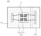
도 1은 본 발명의 일 실시형태에 따른 발광소자 패키지를 개략적으로 나타낸 단면도이다.
도 2는 도 1에 도시된 실시형태에 따른 제1 및 제2 리드 프레임을 상부에서 바라본 개략적인 도면이다.
도 3은 본 발명의 다른 실시형태에 따른 발광소자 패키지를 상부에서 바라본 개략적인 도면이다.
도 4 내지 도 8은 본 발명의 일 실시형태에 따른 발광소자 패키지 제조방법을 나타내기 위한 개략적인 도면이다.1 is a cross-sectional view schematically showing a light emitting device package according to an embodiment of the present invention.
FIG. 2 is a schematic top view of the first and second lead frames according to the embodiment shown in FIG. 1.
3 is a schematic view from above of a light emitting device package according to another embodiment of the present invention.
4 to 8 are schematic views illustrating a method of manufacturing a light emitting device package according to an embodiment of the present invention.
이하, 첨부된 도면을 참조하여 본 발명의 바람직한 실시형태들을 설명한다. Hereinafter, preferred embodiments of the present invention will be described with reference to the accompanying drawings.
그러나, 본 발명의 실시형태는 여러 가지 다른 형태로 변형될 수 있으며, 본 발명의 범위가 이하 설명하는 실시 형태로 한정되는 것은 아니다. 또한, 본 발명의 실시형태는 당해 기술분야에서 평균적인 지식을 가진 자에게 본 발명을 더욱 완전하게 설명하기 위해서 제공되는 것이다. 따라서, 도면에서의 요소들의 형상 및 크기 등은 보다 명확한 설명을 위해 과장될 수 있으며, 도면상의 동일한 부호로 표시되는 요소는 동일한 요소이다.
However, the embodiments of the present invention can be modified into various other forms, and the scope of the present invention is not limited to the embodiments described below. Further, the embodiments of the present invention are provided to more fully explain the present invention to those skilled in the art. Accordingly, the shapes and sizes of the elements in the drawings may be exaggerated for clarity of description, and the elements denoted by the same reference numerals in the drawings are the same elements.
도 1은 본 발명의 일 실시형태에 따른 발광소자 패키지를 개략적으로 나타낸 단면도이며, 도 2는 도 1에 도시된 실시형태에 따른 제1 및 제2 리드 프레임(20a, 20b)을 상부에서 바라본 개략적인 도면이다. 우선, 도 1을 참조하면, 본 발명의 일 실시형태에 따른 발광소자 패키지(100)는, 실장 영역(20a') 및 상기 실장 영역(20a')을 둘러싸는 방열 영역(20a'')을 포함하되, 상기 실장 영역(20a')은 상기 방열 영역(20a'')보다 상부에 위치하도록 상부를 향하여 돌출된 형상을 가지는 제1 리드 프레임(20a)과, 상기 제1 리드 프레임(20a)과 이격 배치되는 제2 리드 프레임(20b)과, 상기 제1 리드 프레임(20a)의 상기 실장 영역(20a')에 배치되는 적어도 하나의 발광소자(10)와, 상기 제1 및 제2 리드 프레임(20a, 20b)을 고정시키도록 상기 제1 및 제2 리드 프레임(20a, 20b) 사이 영역에 형성된 몰딩부(30)와, 상기 발광소자(10) 및 상기 몰딩부(30) 상부에 배치된 렌즈(40)를 포함한다.
1 is a cross-sectional view schematically showing a light emitting device package according to an embodiment of the present invention, Figure 2 is a schematic view of the first and second lead frame (20a, 20b) according to the embodiment shown in FIG. Drawing. First, referring to FIG. 1, a light
상기 발광소자(10)는 전기 신호 인가시 빛을 방출하는 광전 소자라면 어느 것이나 이용 가능하며, 대표적으로, 성장 기판 상에 반도체층을 에피택셜 성장시킨 반도체 발광소자를 이용할 수 있다. 성장기판은 사파이어가 적용될 수 있으나, 이에 한정되는 것은 아니며, 예를 들어 스피넬, SiC, GaN, GaAs 등과 같은 공지된 성장용 기판을 이용할 수 있다. 구체적으로, 상기 발광소자(10)는 BN, SiC, ZnSe, GaN, InGaN, InAlGaN, AlGaN, BAlGaN, BInAlGaN 등으로 이루어질 수 있으며, Si 또는 Zn 등으로 도핑할 수 있다. 또한, 상기 발광소자(10)의 발광층은 InxAlyGa1-x-y(0≤X≤1, 0≤Y≤1, X+Y≤1)로 이루어진 질화물 반도체로 구성될 수 있으며, 단일 또는 다중 양자 우물 구조로 이루어져 출력을 향상시킬 수 있다.
The
도 1에 도시된 바와 같이, 상기 발광소자(10) 상면에 형성된 전극(미도시)은 제1 및 제2 리드 프레임(20a, 20b)과 와이어 본딩되어 외부로부터 전기 신호를 인가받을 수 있다. 본 실시형태의 경우, 발광소자(10) 상면에 형성된 양 전극을 통해 제1 및 제2 리드 프레임(20a, 20b) 각각과 와이어 본딩되는 형태로 도시되어 있으나, 이와는 달리, 발광소자(10)의 실장 영역으로 제공되는 제1 리드 프레임(20a)과는 와이어를 이용하지 않고 직접 전기적으로만 연결되고 제2 리드 프레임(20b)과만 도전성 와이어로 연결되는 등 구체적인 연결 방식은 필요에 따라 다양하게 변경될 수 있다. 또한, 본 실시형태에서는, 하나의 발광소자 패키지(100) 내에 하나의 발광소자(10)가 도시되어 있으나, 상기 제1 리드 프레임(20a) 상에 2개 이상의 발광소자(10)가 배치될 수도 있을 것이다.
As illustrated in FIG. 1, an electrode (not shown) formed on an upper surface of the
제1 및 제2 리드 프레임(20a, 20b)은 발광소자(10)의 실장 영역으로 제공되는 동시에, 상기 발광소자(10)에 외부로부터 공급되는 전기 신호를 인가하기 위한 단자로 기능할 수 있다. 이를 위하여, 상기 한 쌍의 리드 프레임(20a, 20b)은 전기 전도성이 우수한 금속 물질로 이루어질 수 있다. 구체적으로, 도 2a를 참조하면, 상기 제1 리드 프레임(20a)은 실장 영역(20a') 및 상기 실장 영역(20a')을 둘러싸는 방열 영역(20a'')을 포함하되, 상기 실장 영역(20a')은 상기 방열 영역(20a'')보다 상부에 위치하도록 상부를 향하여 돌출된 형상을 가지며, 상기 실장 영역(20a')에는 적어도 하나의 발광소자(10)가 배치될 수 있다. 상기 제1 리드 프레임(20a)의 실장 영역(20a')은 상기 제1 리드 프레임(20a)의 외측이 아닌, 그 내부의 일부 영역만을 상부를 향하여 돌출되도록 형성함으로써 상기 실장 영역(20a')을 둘러싸는 방열 영역(20a'')은 상기 발광소자(10)가 실장된 반대 측에서 외부로 노출되도록 배치될 수 있다.
The first and
본 실시형태에 따르면, 상기 제1 및 제2 리드 프레임(20a, 20b)의 하면 대부분이 외부로 노출되도록 배치되어,발광소자 패키지(100) 실장용 기판과 직접 접촉함으로써, 상기 발광소자(10) 실장 영역(20a')이 상부로 돌출됨으로써 발생할 수 있는 방열 문제를 해결할 수 있다. 구체적으로, 상기 제1 리드 프레임(20a)은 사각형 형상의 상부로 돌출된 실장 영역(20a')을 포함할 수 있으며, 상기 제1 리드 프레임(20a)의 상기 실장 영역(20a')을 둘러싸는 방열 영역(20a'')과 상기 제2 리드 프레임(20b)은 동일 평면상에 위치하여, 상기 제1 및 제2 리드 프레임(20a, 20b) 하면의 적어도 일부가 외부로 노출될 수 있다. 상기 외부로 노출된 제1 및 제2 리드 프레임(20a, 20b)의 표면은 기판, 예를 들면, 에폭시, 트리아진, 실리콘, 폴리이미드 등을 함유하는 유기 수지 소재 및 기타 유기 수지 소재로 형성되거나, AlN, Al2O3 등의 세라믹 소재, 또는 금속 및 금속화합물을 소재로 하여 형성된 PCB 기판에 직접 접촉하도록 배치되어, 상기 발광소자(10)에서 방출된 열을 외부로 효과적으로 전달할 수 있다.
According to the present embodiment, most of the lower surfaces of the first and second lead frames 20a and 20b are disposed to be exposed to the outside, so that the
도 2b는 본 발명의 일 실시형태에 따른 발광소자 패키지에 적용될 수 있는 리드 프레임의 변형 예이다. 도 2b를 참조하면, 도 2a에 도시된 실시형태와는 달리, 상기 제1 리드 프레임(20a)의 일측에서 상기 실장 영역(20a')을 향해 상기 제1 리드 프레임(20a)의 일부가 제거되어 형성된 홈(A)을 더 포함한다. 상기 홈(A)은 상기 제1 및 제2 리드 프레임(20a, 20b)을 고정하기 위한 몰딩 공정에서, 상기 제1 리드 프레임(20a)의 실장 영역(20a') 하부로 몰드 재료가 용이하게 충진되도록 할 수 있으며, 상기 제1 리드 프레임(20a)과 몰딩부(30) 사이의 접착 면적을 넓혀, 접착력을 강화시킬 수 있다. 한편, 상기 제1 및 제2 리드 프레임(20a, 20b)은 복수 개의 관통 홀(H)을 포함하여, 몰딩 공정에서 상기 제1 및 제2 리드 프레임(20a, 20b) 상면 및 하면에 몰드 재료가 배치되도록 할 수 있다.
2B is a modified example of a lead frame that may be applied to a light emitting device package according to an embodiment of the present invention. Referring to FIG. 2B, unlike the embodiment illustrated in FIG. 2A, a portion of the
상기 제1 및 제2 리드 프레임(20a, 20b)을 사이 영역에 형성되어 상기 한 쌍의 리드 프레임을 고정하는 몰딩부(30)는, 상기 제1 및 제2 리드 프레임(20a, 20b)에 형성되되, 상기 발광소자(10)의 상면보다 낮은 위치에 형성될 수 있다. 도 1을 참조하면, 상기 몰딩부(30)는 상기 제1 및 제2 리드 프레임(20a, 20b)의 상면 중 일부 영역이 노출되도록 형성될 수 있으며, 또한, 상기 실장 영역(20a')과 대응하는 상기 제1 리드 프레임(20a')의 하면을 덮도록 형성될 수 있다. 또한, 상기 몰딩부(30)는 상기 제1 및 제2 리드 프레임(20a, 20b)의 상면 중 적어도 일부를 노출하도록 형성될 수 있으며, 상기 노출된 면을 통해 상기 발광소자(10)와 와이어 본딩될 수 있다.
The
상기 몰딩부(30)는 상기 발광소자(10)의 상면보다 낮은 곳에 형성되어, 상기 발광소자(10)로부터 방출된 광을 상부로 반사하는 기능이 요구되지 않으므로, 일반적으로 발광소자 패키지에 사용되는 백색 또는 투명 성형 재료가 적용되어야 하는 것은 아니다. 즉, 종래에는 상기 발광소자의 측면을 감싸는 형태로 몰딩부가 형성됨에 따라, 발광소자로부터 방출된 빛을 측면 및 하면에서 반사하여 상부로 유도하기 위하여 광 반사 기능을 갖는 백색 성형재료를 사용할 것이 요구되었으나, 본 발명의 경우, 상기 몰딩부(30)가 상기 발광소자(10)의 상면보다 낮은 위치에 형성되므로, 상기 몰딩부(30)가 광 반사 기능을 요구하지 않게 되어, 고온으로 인한 백색의 몰드 소재 변색에 의해 발생하는 휘도 저하 문제를 방지할 수 있다. 또한, 고 접착력, 고 신뢰성, 고 내열성, 고 난연성, 우수한 기계적 물성을 갖는 유색 몰드 재료, 예를 들면, EMC(Epoxy molding compound) 및 다양한 색상을 첨가한 몰드 재료가 적용될 수 있다.
Since the
한편, 구체적으로 도시하지는 않았으나, 상기 발광구조물(10)의 광 방출면에 중 적어도 일부에는 파장 변환용 형광체를 포함하는 형광체층(미도시)이 형성될 수 있다. 상기 형광체층은 상기 발광소자(10)의 활성층으로부터 방출된 광의 파장을 변환시키는 파장변환용 형광체 입자를 포함할 수 있다. 상기 형광체는 황색(yellow), 적색(red) 및 녹색(green) 중 어느 하나로 파장을 변환시키는 형광체로 이루어질 수 있으며, 상기 형광체의 종류는, 상기 발광소자(10)의 활성층으로부터 방출되는 파장에 의해 결정될 수 있다. 구체적으로, 상기 형광체층은 YAG계, TAG계, Silicate계, Sulfide계 또는 Nitride계 중 어느 하나의 형광물질을 포함할 수 있다. 예를 들면, 청색 발광 LED 칩에 황색으로 파장 변환시키는 형광체를 적용하는 경우, 백색 발광 반도체 발광소자를 얻을 수 있다.
Although not specifically illustrated, a phosphor layer (not shown) including a phosphor for converting wavelengths may be formed on at least part of the light emitting surface of the
상기 발광소자(10) 상부에는 렌즈(40)가 배치될 수 있다. 구체적으로, 제1 리드프레임(20a) 상에 발광소자(10)를 배치한 후, 상기 발광소자(10) 상면을 수지로 디스펜싱(dispencing) 혹은 몰딩(molding)하여 다양한 형상의 렌즈, 예를 들면, 반구 형상의 투명 렌즈를 성형하여 광 추출 효율을 향상시킬 수 있다. 상기 렌즈(40)는 상기 발광소자(10)를 완전히 커버하여 발광소자(10)를 보호할 뿐 아니라, 반구 형상으로 이루어져, 경계면에서의 프레넬 반사를 줄여서 광추출을 증가시키는 역할을 할 수 있다. 이때, 상기 렌즈(40)는 수지로 이루어져 있으며, 상기 수지는, 에폭시, 실리콘, 변형 실리콘, 우레탄수지, 옥세탄수지, 아크릴, 폴리카보네이트 및 폴리이미드 중 어느 하나를 포함할 수 있다. 또한, 상기 렌즈 상면에 요철을 형성하여 광추출 효율을 높이고, 방출되는 광의 방향을 조절할 수 있다. 이에 제한되는 것은 아니나, 상기 렌즈(40)는 상기 몰드부(30)와 상이한 물질로 이루어질 수 있으며, 예를 들면, 상기 렌즈(40)는 광이 효율적으로 투과할 수 있도록 투명 수지로 형성되고, 상기 몰드부(30)는 고 기능성 유색 수지로 형성될 수 있다.
The
도 3은 본 발명의 다른 실시형태에 따른 발광소자 패키지를 상부에서 바라본 개략적인 도면이다. 본 실시형태에 따른 발광소자 패키지(101)는, 실장 영역(21a') 및 상기 실장 영역(21a')을 둘러싸는 방열 영역(21a'')을 포함하되, 상기 실장 영역(21a')은 상기 방열 영역(21a'')보다 상부에 위치하도록 상부를 향하여 돌출된 형상의 제1 리드 프레임(21a)과, 상기 제1 리드 프레임(21a)과 이격 배치되는 제2 리드 프레임(21b)을 포함하며, 상기 제1 리드 프레임(21a)의 실장 영역(21a')에는 복수 개의 발광소자(11)가 배치될 수 있다. 다만, 도 3에서는 상기 발광소자(11) 상면에 배치되는 렌즈(미도시)의 도시를 생략하였으며, 상기 제1 리드 프레임(21a)의 실장 영역(21a')에 복수 개의 발광소자(11)가 배치된다는 점에서만 도 1에 도시된 실시형태와 상이하다.
3 is a schematic view from above of a light emitting device package according to another embodiment of the present invention. The light emitting
도 3을 참조하면, 상기 제1 리드 프레임(21a)의 실장 영역(21a')에는 4개의 발광소자(11)가 배치되며, 상기 발광소자(11)는 상호 직렬 및 병렬로 연결될 수 있다. 상기 제1 및 제2 리드 프레임(21a, 21b)은 일정 간격 이격 배치되어 상호 전기적으로 분리되어 있으며, 그 사이 및 상면에 몰드부(31)가 형성될 수 있다. 상기 몰드부(31)는 상기 제1 및 제2 리드 프레임(21a, 21b)의 상면 중 적어도 일부를 노출하며, 상기 노출된 영역을 통해 상기 발광소자(11)와 상기 제1 및 제2 리드 프레임(21a, 21b) 각각이 와이어 본딩될 수 있다. 다만, 전술한 바와 같이, 상기 발광소자(11)의 전기적 연결 형태는 상기 발광소자(11)가 실장된 제1 리드 프레임(21a)과는 직접 연결되고, 제2 리드 프레임(21b)과만 와이어 본딩되는 등 다양하게 변형될 수 있음은 물론이다.
Referring to FIG. 3, four light emitting
도 4 내지 도 8은 본 발명의 일 실시형태에 따른 발광소자 패키지 제조방법을 나타내기 위한 개략적인 도면이다. 구체적으로, 도 1에 도시된 실시형태에 따른 발광소자 패키지(100)를 제조하기 위한 공정 단면도로, 우선, 도 4를 참조하면, 실장 영역(20a') 및 상기 실장 영역(20a')을 둘러싸는 방열 영역(20a'')을 형성하되, 상기 실장 영역(20a')이 상부를 향하여 돌출되어 상기 방열 영역(20a'')보다 상부에 위치하는 형상을 갖도록 제1 및 제2 리드 프레임(20a, 20b) 중 적어도 하나를 프레스 가공할 수 있다. 본 실시형태에서는, 실장 영역(20a')과 상기 실장 영역(20a')을 둘러싸는 방열 영역(20a'')이 형성된 동일한 리드 프레임을 복수 개 배열하였으나, 이와는 달리, 상기 실장 영역(20a')이 상부를 향하여 돌출되어 상기 방열 영역(20a'')보다 상부에 위치하는 형상을 갖는 제1 리드 프레임(20a)과, 평판 형상의 제2 리드 프레임(20b)을 상기 제1 리드 프레임(20a)과 상호 교대로 이격 배치할 수 있다.
4 to 8 are schematic views illustrating a method of manufacturing a light emitting device package according to an embodiment of the present invention. Specifically, a cross-sectional view of a process for manufacturing the light emitting
도 4는 상기 리드 프레임(20)의 상부를 향하여 돌출되도록 형성되는 실장 영역(20a')을 가로지르는 절단 영역을 개략적으로 나타낸 것으로, 상부에서 바라보는 경우, 상기 리드 프레임(20)이 전체적으로 절곡되어 상부로 돌출되는 것이 아니라, 상기 방열 영역(20a'')에 의해 둘러싸이는 실장 영역(20a')만이 상부를 향하여 돌출된 형태가 된다. 즉, 발광 소자가 실장될 영역을 제외한 방열 영역(20a'')은 상기 실장 영역(20a')보다 낮은 위치에서, 동일 평면상에 위치하게 된다. 이러한 형상은, 평판 형태의 리드 프레임의 중앙 부근 영역을 프레스 가공하여 형성할 수 있다.
FIG. 4 schematically shows a cutting area across the mounting
다음으로, 도 5를 참조하면, 본 실시형태에 따른 발광소자 패키지를 제조하기 위한 패키지 제조장치는, 몰딩부(30)와 동일한 형상의 캐비티를 갖는 하부 금형(50a) 및 상부 금형(50b)으로 구성된다. 상기 하부 및 상부 금형(50a, 50b) 사이에 형성된 캐비티 내로 몰딩부(30) 제조용 수지 조성물이 용융되어 공급되어 원하는 형상의 발광소자 패키지 구조물을 제조할 수 있다. 구체적으로, 상기 하부 및 상부 금형(50a, 50b) 사이에 리드 프레임(20)이 배치되고, 상부 금형(50b)의 하면이 하부 금형(50a)의 상면에 가압 밀착된 상태에서 고온으로 가열되어 일정한 점도를 갖는 겔(gel) 상태의 성형 수지로 용융되어 상부 및 하부 금형(50b, 50a) 사이로 주입된다. 이에 제한되는 것은 아니나, 상기 몰딩부(30)는 상기 실장 영역(20a')과 동일한 높이를 갖도록 형성될 수 있으며, 상기 실장 영역(20a')에 대응하는 상기 리드 프레임(20) 하면에 형성되는 빈공간에도 성형 재료가 채워져, 보다 견고한 결합이 가능하도록 할 수 있다. 또한, 상기 몰딩부(30)를 형성하는 몰드 재료는, 이에 제한되는 것은 아니나, 고 접착력, 고 신뢰성, 고 내열성, 고 난연성, 우수한 기계적 물성을 갖는 유색 몰드 재료, 예를 들면, EMC(Epoxy molding compound) 및 다양한 색상을 첨가한 몰드 재료가 적용될 수 있다.
Next, referring to FIG. 5, the package manufacturing apparatus for manufacturing the light emitting device package according to the present embodiment includes a
다음으로, 도 6 에 도시된 바와 같이, 상기 리드 프레임(20)이 부착된 몰딩부(30)의 성형이 완료된 후에는 상부 금형(50b) 및 하부 금형(50a)이 상하로 분리된다. 상기 몰드부(30)에 의해 고정된 리드 프레임(20)의 인접한 주위 영역으로부터 돌출된 실장 영역(20a')에, 발광소자(10)를 배치하고, 상기 몰드부(30)에 의해 노출되는 리드 프레임(20)의 표면과 와이어 본딩 할 수 있다. 전술한 바와 같이, 상기 리드 프레임(20)과 발광소자(10)의 전기적 연결관계는 이에 제한되는 것은 아니며, 다양하게 변형될 수 있을 것이다.
Next, as shown in FIG. 6, after the molding of the
다음으로, 도 7에 도시된 바와 같이, 상기 발광소자(10) 상부에 렌즈(40)를 배치할 수 있다. 이때, 상기 렌즈(40)는 발광소자(10) 상면을 수지로 디스펜싱(dispencing) 혹은 몰딩(molding)하여 다양한 형상의 렌즈, 예를 들면, 반구 형상의 투명 렌즈를 성형할 수 있으며, 이때, 상기 렌즈 상면에 요철을 형성하여 광추출 효율을 높이고, 방출되는 광의 방향을 조절할 수 있다. 상기 렌즈(40)는 수지로 이루어져 있으며, 상기 수지는, 에폭시, 실리콘, 변형 실리콘, 우레탄수지, 옥세탄수지, 아크릴, 폴리카보네이트 및 폴리이미드 중 어느 하나를 포함할 수 있다. 또한, 상기 렌즈 상면에 요철을 형성하여 광추출 효율을 높이고, 방출되는 광의 방향을 조절할 수 있다. 이에 제한되는 것은 아니나, 상기 렌즈(40)는 상기 몰드부(30)와 서로 다른 상이한 물질로 이루어질 수 있으며, 구체적으로, 상기 렌즈(40)는 광이 효율적으로 투과할 수 있도록 투명 수지로 형성되고, 상기 몰드부(30)는 고 기능성 유색 수지로 형성될 수 있다.
Next, as shown in FIG. 7, the
다음으로, 도 8에 도시된 바와 같이, 상기 리드 프레임(20)을 개별 패키지 단위로 분리하여, 복수 개의 발광소자 패키지(100)를 제조할 수 있다. 상기 분리 공정은, 물리적, 화학적 절삭, 식각 공정 등이 적용될 수 있다. 본 실시형태와 달리, 한 쌍의 리드 프레임(20a, 20b)이 상호 교대로 이격 배치되어 발광소자 패키지(100) 사이에 몰드부(30)가 존재하는 경우에는, 리드 프레임(20)을 구성하는 금속 절단 공정이 요구되지 않으므로, 패키지 단위의 분리 공정이 보다 용이하게 이루어질 수 있다. 또한, 본 실시형태와 같이, 복수의 발광소자 패키지를 하나의 공정에서 제조하여 분리하는 경우뿐만 아니라, 개별 발광소자 패키지 단위로 제조되는 것도 가능함은 물론이다.
Next, as shown in FIG. 8, the
본 발명은 상술한 실시 형태 및 첨부된 도면에 의해 한정되는 것이 아니며, 첨부된 청구범위에 의해 한정하고자 한다. 따라서, 청구범위에 기재된 본 발명의 기술적 사상을 벗어나지 않는 범위 내에서 당 기술분야의 통상의 지식을 가진 자에 의해 다양한 형태의 치환, 변형 및 변경이 가능할 것이며, 이 또한 본 발명의 범위에 속한다고 할 것이다.The present invention is not limited by the above-described embodiments and the accompanying drawings, but is intended to be limited only by the appended claims. It will be apparent to those skilled in the art that various changes in form and details may be made therein without departing from the spirit and scope of the invention as defined by the appended claims. something to do.
100, 101: 발광소자 패키지 10, 11: 발광소자
20a, 21a: 제1 리드 프레임 20b, 21b: 제2 리드 프레임
30, 31: 몰딩부 40: 렌즈
50a, 50b: 하부, 상부 금형100 and 101: light emitting
20a, 21a: first
30, 31: molding 40: lens
50a, 50b: lower, upper mold
Claims (18)
상기 제1 리드 프레임과 이격 배치되는 제2 리드 프레임;
상기 제1 리드 프레임의 상기 실장 영역에 배치된 적어도 하나의 발광소자;
상기 제1 및 제2 리드 프레임을 고정시키도록 상기 제1 및 제2 리드 프레임 사이 영역에 형성된 몰딩부; 및
상기 발광소자 및 상기 몰딩부의 상부에 배치된 렌즈;
를 포함하는 발광소자 패키지.
A first lead frame including a mounting area and a heat dissipation area surrounding the mounting area, the mounting area protruding upward to be positioned above the heat dissipation area;
A second lead frame spaced apart from the first lead frame;
At least one light emitting element disposed in the mounting region of the first lead frame;
A molding part formed in an area between the first and second lead frames to fix the first and second lead frames; And
A lens disposed on the light emitting element and the molding part;
Light emitting device package comprising a.
상기 몰딩부는 상기 제1 및 제2 리드 프레임 상면에 형성되되, 상기 발광소자의 상면보다 낮은 위치에 형성되는 것을 특징으로 하는 발광소자 패키지.
The method of claim 1,
The molding unit is formed on the upper surface of the first and second lead frame, the light emitting device package, characterized in that formed in a lower position than the upper surface of the light emitting device.
상기 몰딩부는 상기 실장영역에 대응하는 상기 제1 리드 프레임의 하면을 덮도록 형성되는 것을 특징으로 하는 발광소자 패키지.
The method of claim 1,
And the molding part is formed to cover a lower surface of the first lead frame corresponding to the mounting area.
상기 몰딩부와 상기 렌즈는 서로 상이한 물질로 이루어진 것을 특징으로 하는 발광소자 패키지.
The method of claim 1,
The molding unit and the lens is a light emitting device package, characterized in that made of different materials.
상기 몰딩부는 유색 수지로 이루어진 것을 특징으로 하는 발광소자 패키지.
The method of claim 1,
The molding unit light emitting device package, characterized in that made of colored resin.
상기 제1 리드 프레임은 사각형 형상의 상부로 돌출된 실장 영역을 포함하며, 상기 제1 리드 프레임의 방열 영역과 상기 제2 리드 프레임은 동일 평면상에 배치되는 것을 특징으로 하는 발광소자 패키지.
The method of claim 1,
The first lead frame includes a mounting area protruding upward in a quadrangular shape, wherein the heat dissipation area of the first lead frame and the second lead frame are disposed on the same plane.
상기 제1 및 제2 리드 프레임 중 적어도 하나는, 그 하면의 적어도 일부가 외부로 노출되는 것을 특징으로 하는 발광소자 패키지.
The method of claim 1,
At least one of the first and second lead frames, the light emitting device package, characterized in that at least a portion of the lower surface is exposed to the outside.
상기 몰딩부는 상기 제1 및 제2 리드 프레임의 상면 중 적어도 일부를 노출하며, 상기 노출된 면을 통해 상기 발광소자와 와이어 본딩되는 것을 특징으로 하는 발광소자 패키지.
The method of claim 1,
The molding unit exposes at least a portion of upper surfaces of the first and second lead frames, and the light emitting device package, characterized in that the wire bonding with the light emitting device through the exposed surface.
상기 제1 및 제2 리드 프레임 중 적어도 하나에 형성된 관통 홀을 포함하는 것을 특징으로 하는 발광소자 패키지.
The method of claim 1,
And a through-hole formed in at least one of the first and second lead frames.
상기 제1 리드 프레임의 일측에서 상기 실장 영역을 향해 상기 제1 리드 프레임의 일부가 제거되어 형성된 홈을 더 포함하는 것을 특징으로 하는 발광소자 패키지.
The method of claim 1,
And a groove formed by removing a portion of the first lead frame from one side of the first lead frame toward the mounting region.
상기 홈은 상기 제2 리드 프레임과 마주보는 방향에 형성된 것을 특징으로 하는 발광소자 패키지.
The method of claim 10,
The groove is a light emitting device package, characterized in that formed in the direction facing the second lead frame.
상기 발광소자의 광 방출면 중 적어도 일부에 형성된 형광체층을 더 포함하는 것을 특징으로 하는 발광소자 패키지.
The method of claim 1,
The light emitting device package further comprises a phosphor layer formed on at least part of the light emitting surface of the light emitting device.
이격 배치된 상기 제1 및 제2 리드 프레임 사이 영역에 몰딩부를 형성하여, 상기 제1 및 제2 리드 프레임을 고정시키는 단계;
상기 실장 영역 상에 적어도 하나의 발광소자를 배치하는 단계; 및
상기 발광소자 상부에 렌즈를 배치하는 단계;
를 포함하는 발광소자 패키지 제조방법.
Forming a mounting area and a heat dissipation area surrounding the mounting area, and press-processing at least one of the first and second lead frames such that the mounting area protrudes upward to have a shape located above the heat dissipation area. ;
Fixing the first and second lead frames by forming a molding part in an area between the first and second lead frames spaced apart from each other;
Disposing at least one light emitting device on the mounting area; And
Disposing a lens on the light emitting device;
Emitting device package.
상기 제1 및 제2 리드 프레임 중 적어도 하나는, 그 하면의 적어도 일부가 외부로 노출되도록 형성되는 것을 특징으로 하는 발광소자 패키지 제조방법.
The method of claim 13,
At least one of the first and second lead frames, the light emitting device package manufacturing method, characterized in that the at least a portion of the lower surface is formed to be exposed to the outside.
상기 몰딩부는 상기 제1 및 제2 리드 프레임 상면에 형성되되, 상기 발광소자의 상면보다 낮은 위치에 형성되는 것을 특징으로 하는 발광소자 패키지 제조방법.
The method of claim 13,
The molding part is formed on the upper surface of the first and second lead frame, the light emitting device package manufacturing method, characterized in that formed in a lower position than the upper surface of the light emitting device.
상기 몰딩부는 상기 실장영역에 대응하는 상기 제1 리드 프레임의 하면을 덮도록 형성되는 것을 특징으로 하는 발광소자 패키지 제조방법.
The method of claim 13,
And the molding part is formed to cover a lower surface of the first lead frame corresponding to the mounting area.
상기 몰딩부는 유색 수지로 이루어진 것을 특징으로 하는 발광소자 패키지 제조방법.
The method of claim 13,
The molding part manufacturing method of a light emitting device package, characterized in that made of colored resin.
상기 발광소자를 상기 제1 및 제2 리드 프레임 중 적어도 하나와 와이어 본딩하는 단계를 더 포함하는 것을 특징으로 하는 발광소자 패키지 제조방법.The method of claim 13,
And wire bonding the light emitting device to at least one of the first and second lead frames.
Priority Applications (3)
| Application Number | Priority Date | Filing Date | Title |
|---|---|---|---|
| KR1020110013385A KR20120093679A (en) | 2011-02-15 | 2011-02-15 | Light emitting device package and manufacturing method thereof |
| US13/356,245 US20120205696A1 (en) | 2011-02-15 | 2012-01-23 | Light emitting device package and method of manufacturing thereof |
| CN201210031251.7A CN102637812B (en) | 2011-02-15 | 2012-02-13 | Light emitting device package and manufacturing method thereof |
Applications Claiming Priority (1)
| Application Number | Priority Date | Filing Date | Title |
|---|---|---|---|
| KR1020110013385A KR20120093679A (en) | 2011-02-15 | 2011-02-15 | Light emitting device package and manufacturing method thereof |
Publications (1)
| Publication Number | Publication Date |
|---|---|
| KR20120093679A true KR20120093679A (en) | 2012-08-23 |
Family
ID=46622127
Family Applications (1)
| Application Number | Title | Priority Date | Filing Date |
|---|---|---|---|
| KR1020110013385A Withdrawn KR20120093679A (en) | 2011-02-15 | 2011-02-15 | Light emitting device package and manufacturing method thereof |
Country Status (3)
| Country | Link |
|---|---|
| US (1) | US20120205696A1 (en) |
| KR (1) | KR20120093679A (en) |
| CN (1) | CN102637812B (en) |
Cited By (1)
| Publication number | Priority date | Publication date | Assignee | Title |
|---|---|---|---|---|
| KR20140088021A (en) * | 2012-12-29 | 2014-07-09 | 니치아 카가쿠 고교 가부시키가이샤 | Light emitting device package, light emitting device using that package, and illumination device using the light emitting devices |
Families Citing this family (6)
| Publication number | Priority date | Publication date | Assignee | Title |
|---|---|---|---|---|
| KR101958418B1 (en) * | 2013-02-22 | 2019-03-14 | 삼성전자 주식회사 | Light emitting device package |
| CN103268914A (en) * | 2013-05-27 | 2013-08-28 | 北京半导体照明科技促进中心 | LED package substrate and manufacturing process |
| DE102013219063A1 (en) * | 2013-09-23 | 2015-03-26 | Osram Opto Semiconductors Gmbh | Optoelectronic component and method for its production |
| KR102261288B1 (en) * | 2017-03-14 | 2021-06-04 | 현대자동차 주식회사 | Light emitting diode package for automobile exterior |
| US11677059B2 (en) | 2017-04-26 | 2023-06-13 | Samsung Electronics Co., Ltd. | Light-emitting device package including a lead frame |
| KR102335216B1 (en) * | 2017-04-26 | 2021-12-03 | 삼성전자 주식회사 | Light emitting device package |
Family Cites Families (24)
| Publication number | Priority date | Publication date | Assignee | Title |
|---|---|---|---|---|
| US5436492A (en) * | 1992-06-23 | 1995-07-25 | Sony Corporation | Charge-coupled device image sensor |
| TW351008B (en) * | 1996-12-24 | 1999-01-21 | Matsushita Electronics Corp | Lead holder, manufacturing method of lead holder, semiconductor and manufacturing method of semiconductor |
| DE19829197C2 (en) * | 1998-06-30 | 2002-06-20 | Siemens Ag | Component emitting and / or receiving radiation |
| US6208020B1 (en) * | 1999-02-24 | 2001-03-27 | Matsushita Electronics Corporation | Leadframe for use in manufacturing a resin-molded semiconductor device |
| DE19918370B4 (en) * | 1999-04-22 | 2006-06-08 | Osram Opto Semiconductors Gmbh | LED white light source with lens |
| US6720207B2 (en) * | 2001-02-14 | 2004-04-13 | Matsushita Electric Industrial Co., Ltd. | Leadframe, resin-molded semiconductor device including the leadframe, method of making the leadframe and method for manufacturing the device |
| JP2003204027A (en) * | 2002-01-09 | 2003-07-18 | Matsushita Electric Ind Co Ltd | Lead frame and method of manufacturing the same, resin-sealed semiconductor device and method of manufacturing the same |
| JP4572312B2 (en) * | 2004-02-23 | 2010-11-04 | スタンレー電気株式会社 | LED and manufacturing method thereof |
| JP2005317661A (en) * | 2004-04-27 | 2005-11-10 | Sharp Corp | Semiconductor light emitting device and manufacturing method thereof |
| JP4953578B2 (en) * | 2005-02-18 | 2012-06-13 | 日亜化学工業株式会社 | Light emitting device |
| KR100616684B1 (en) * | 2005-06-03 | 2006-08-28 | 삼성전기주식회사 | High output LED package and manufacturing method |
| CN101807533B (en) * | 2005-06-30 | 2016-03-09 | 费查尔德半导体有限公司 | Semiconductor die package and manufacturing method thereof |
| KR100700883B1 (en) * | 2005-12-14 | 2007-03-29 | 엘지전자 주식회사 | Light emitting device package and manufacturing method thereof |
| JP2007311445A (en) * | 2006-05-17 | 2007-11-29 | Stanley Electric Co Ltd | Semiconductor light emitting device and manufacturing method thereof |
| US8044418B2 (en) * | 2006-07-13 | 2011-10-25 | Cree, Inc. | Leadframe-based packages for solid state light emitting devices |
| KR100851636B1 (en) * | 2006-07-27 | 2008-08-13 | 삼성전기주식회사 | Surface-Mount LED Elements |
| US7604028B2 (en) * | 2006-07-27 | 2009-10-20 | Bridgefarmer Donnie R | Front pocket wallet |
| JP2008060344A (en) * | 2006-08-31 | 2008-03-13 | Toshiba Corp | Semiconductor light emitting device |
| JP2008108836A (en) * | 2006-10-24 | 2008-05-08 | Sharp Corp | Semiconductor light emitting device and manufacturing method thereof |
| JP4205135B2 (en) * | 2007-03-13 | 2009-01-07 | シャープ株式会社 | Semiconductor light emitting device, multiple lead frame for semiconductor light emitting device |
| KR100818518B1 (en) * | 2007-03-14 | 2008-03-31 | 삼성전기주식회사 | LED Package |
| KR101574286B1 (en) * | 2009-01-21 | 2015-12-04 | 삼성전자 주식회사 | Light emitting device |
| KR101047676B1 (en) * | 2010-04-01 | 2011-07-08 | 엘지이노텍 주식회사 | Light emitting device and light unit having same |
| US8987022B2 (en) * | 2011-01-17 | 2015-03-24 | Samsung Electronics Co., Ltd. | Light-emitting device package and method of manufacturing the same |
-
2011
- 2011-02-15 KR KR1020110013385A patent/KR20120093679A/en not_active Withdrawn
-
2012
- 2012-01-23 US US13/356,245 patent/US20120205696A1/en not_active Abandoned
- 2012-02-13 CN CN201210031251.7A patent/CN102637812B/en not_active Expired - Fee Related
Cited By (1)
| Publication number | Priority date | Publication date | Assignee | Title |
|---|---|---|---|---|
| KR20140088021A (en) * | 2012-12-29 | 2014-07-09 | 니치아 카가쿠 고교 가부시키가이샤 | Light emitting device package, light emitting device using that package, and illumination device using the light emitting devices |
Also Published As
| Publication number | Publication date |
|---|---|
| US20120205696A1 (en) | 2012-08-16 |
| CN102637812B (en) | 2014-12-03 |
| CN102637812A (en) | 2012-08-15 |
Similar Documents
| Publication | Publication Date | Title |
|---|---|---|
| US7872410B2 (en) | Light emitting device and light emitter | |
| EP1692729B1 (en) | Submount for a semiconductor light emitting device and manufacturing method thereof | |
| KR101543333B1 (en) | Lead frame for light emitting device package, light emitting device package, and illumination apparatus employing the light emitting device package | |
| US9893247B2 (en) | Light-emitting device including phosphorus layer covering side surfaces of substrate and light-emitting device package including the same | |
| US20190206846A1 (en) | Light emitting device package and light emitting device package module including the same | |
| KR20120093679A (en) | Light emitting device package and manufacturing method thereof | |
| US20150349219A1 (en) | Light emitting device module | |
| JP2012134295A (en) | Semiconductor light-emitting device and method of manufacturing the same | |
| CN107565009A (en) | Led module | |
| CN109390449A (en) | Light emitting device package | |
| KR101607139B1 (en) | Light emitting device package, backlight unit, illumination device and its manufacturing method | |
| KR101186644B1 (en) | Led package mounting a led having an array of light emitting cells coupled in series | |
| JP4016925B2 (en) | Light emitting device | |
| KR20060136100A (en) | Led package mounting a led having an array of light emitting cells coupled in series | |
| KR101719642B1 (en) | Light-emitting diode package and method of manufacturing the same | |
| KR101713685B1 (en) | Light emitting device package, backlight unit and light emitting apparatus manufacturing method | |
| KR101273481B1 (en) | White Light-emitting diode and Method of Manufacturing the same | |
| KR20120079667A (en) | Light emitting device package and manufacturing method thereof | |
| KR101547548B1 (en) | Phosphor encapsulation type light emitting device package, backlight unit, illumination device and its manufacturing method | |
| JP6978708B2 (en) | Semiconductor light emitting device | |
| JP4742772B2 (en) | Light emitting device | |
| KR101258231B1 (en) | Led package mounting a led | |
| KR20130024499A (en) | Light emitting module | |
| JP2022010198A (en) | Semiconductor light emitting device | |
| KR20120060084A (en) | Light Source Module |
Legal Events
| Date | Code | Title | Description |
|---|---|---|---|
| PA0109 | Patent application |
Patent event code: PA01091R01D Comment text: Patent Application Patent event date: 20110215 |
|
| N231 | Notification of change of applicant | ||
| PN2301 | Change of applicant |
Patent event date: 20120629 Comment text: Notification of Change of Applicant Patent event code: PN23011R01D |
|
| PG1501 | Laying open of application | ||
| PC1203 | Withdrawal of no request for examination | ||
| WITN | Application deemed withdrawn, e.g. because no request for examination was filed or no examination fee was paid |