KR20120067205A - Backlight unit, liquid crystal display device and method assembling thereof - Google Patents
Backlight unit, liquid crystal display device and method assembling thereof Download PDFInfo
- Publication number
- KR20120067205A KR20120067205A KR1020100128670A KR20100128670A KR20120067205A KR 20120067205 A KR20120067205 A KR 20120067205A KR 1020100128670 A KR1020100128670 A KR 1020100128670A KR 20100128670 A KR20100128670 A KR 20100128670A KR 20120067205 A KR20120067205 A KR 20120067205A
- Authority
- KR
- South Korea
- Prior art keywords
- light
- liquid crystal
- guide plate
- tape
- leds
- Prior art date
- Legal status (The legal status is an assumption and is not a legal conclusion. Google has not performed a legal analysis and makes no representation as to the accuracy of the status listed.)
- Ceased
Links
Images



Classifications
-
- G—PHYSICS
- G02—OPTICS
- G02F—OPTICAL DEVICES OR ARRANGEMENTS FOR THE CONTROL OF LIGHT BY MODIFICATION OF THE OPTICAL PROPERTIES OF THE MEDIA OF THE ELEMENTS INVOLVED THEREIN; NON-LINEAR OPTICS; FREQUENCY-CHANGING OF LIGHT; OPTICAL LOGIC ELEMENTS; OPTICAL ANALOGUE/DIGITAL CONVERTERS
- G02F1/00—Devices or arrangements for the control of the intensity, colour, phase, polarisation or direction of light arriving from an independent light source, e.g. switching, gating or modulating; Non-linear optics
- G02F1/01—Devices or arrangements for the control of the intensity, colour, phase, polarisation or direction of light arriving from an independent light source, e.g. switching, gating or modulating; Non-linear optics for the control of the intensity, phase, polarisation or colour
- G02F1/13—Devices or arrangements for the control of the intensity, colour, phase, polarisation or direction of light arriving from an independent light source, e.g. switching, gating or modulating; Non-linear optics for the control of the intensity, phase, polarisation or colour based on liquid crystals, e.g. single liquid crystal display cells
- G02F1/133—Constructional arrangements; Operation of liquid crystal cells; Circuit arrangements
- G02F1/1333—Constructional arrangements; Manufacturing methods
- G02F1/1335—Structural association of cells with optical devices, e.g. polarisers or reflectors
- G02F1/1336—Illuminating devices
-
- G—PHYSICS
- G02—OPTICS
- G02B—OPTICAL ELEMENTS, SYSTEMS OR APPARATUS
- G02B6/00—Light guides; Structural details of arrangements comprising light guides and other optical elements, e.g. couplings
- G02B6/0001—Light guides; Structural details of arrangements comprising light guides and other optical elements, e.g. couplings specially adapted for lighting devices or systems
- G02B6/0011—Light guides; Structural details of arrangements comprising light guides and other optical elements, e.g. couplings specially adapted for lighting devices or systems the light guides being planar or of plate-like form
- G02B6/0033—Means for improving the coupling-out of light from the light guide
- G02B6/005—Means for improving the coupling-out of light from the light guide provided by one optical element, or plurality thereof, placed on the light output side of the light guide
- G02B6/0053—Prismatic sheet or layer; Brightness enhancement element, sheet or layer
-
- G—PHYSICS
- G02—OPTICS
- G02B—OPTICAL ELEMENTS, SYSTEMS OR APPARATUS
- G02B6/00—Light guides; Structural details of arrangements comprising light guides and other optical elements, e.g. couplings
- G02B6/0001—Light guides; Structural details of arrangements comprising light guides and other optical elements, e.g. couplings specially adapted for lighting devices or systems
- G02B6/0011—Light guides; Structural details of arrangements comprising light guides and other optical elements, e.g. couplings specially adapted for lighting devices or systems the light guides being planar or of plate-like form
- G02B6/0033—Means for improving the coupling-out of light from the light guide
- G02B6/005—Means for improving the coupling-out of light from the light guide provided by one optical element, or plurality thereof, placed on the light output side of the light guide
- G02B6/0055—Reflecting element, sheet or layer
-
- G—PHYSICS
- G02—OPTICS
- G02B—OPTICAL ELEMENTS, SYSTEMS OR APPARATUS
- G02B6/00—Light guides; Structural details of arrangements comprising light guides and other optical elements, e.g. couplings
- G02B6/0001—Light guides; Structural details of arrangements comprising light guides and other optical elements, e.g. couplings specially adapted for lighting devices or systems
- G02B6/0011—Light guides; Structural details of arrangements comprising light guides and other optical elements, e.g. couplings specially adapted for lighting devices or systems the light guides being planar or of plate-like form
- G02B6/0065—Manufacturing aspects; Material aspects
-
- G—PHYSICS
- G02—OPTICS
- G02B—OPTICAL ELEMENTS, SYSTEMS OR APPARATUS
- G02B6/00—Light guides; Structural details of arrangements comprising light guides and other optical elements, e.g. couplings
- G02B6/0001—Light guides; Structural details of arrangements comprising light guides and other optical elements, e.g. couplings specially adapted for lighting devices or systems
- G02B6/0011—Light guides; Structural details of arrangements comprising light guides and other optical elements, e.g. couplings specially adapted for lighting devices or systems the light guides being planar or of plate-like form
- G02B6/0081—Mechanical or electrical aspects of the light guide and light source in the lighting device peculiar to the adaptation to planar light guides, e.g. concerning packaging
- G02B6/0093—Means for protecting the light guide
-
- G—PHYSICS
- G02—OPTICS
- G02F—OPTICAL DEVICES OR ARRANGEMENTS FOR THE CONTROL OF LIGHT BY MODIFICATION OF THE OPTICAL PROPERTIES OF THE MEDIA OF THE ELEMENTS INVOLVED THEREIN; NON-LINEAR OPTICS; FREQUENCY-CHANGING OF LIGHT; OPTICAL LOGIC ELEMENTS; OPTICAL ANALOGUE/DIGITAL CONVERTERS
- G02F1/00—Devices or arrangements for the control of the intensity, colour, phase, polarisation or direction of light arriving from an independent light source, e.g. switching, gating or modulating; Non-linear optics
- G02F1/01—Devices or arrangements for the control of the intensity, colour, phase, polarisation or direction of light arriving from an independent light source, e.g. switching, gating or modulating; Non-linear optics for the control of the intensity, phase, polarisation or colour
- G02F1/13—Devices or arrangements for the control of the intensity, colour, phase, polarisation or direction of light arriving from an independent light source, e.g. switching, gating or modulating; Non-linear optics for the control of the intensity, phase, polarisation or colour based on liquid crystals, e.g. single liquid crystal display cells
- G02F1/133—Constructional arrangements; Operation of liquid crystal cells; Circuit arrangements
- G02F1/1333—Constructional arrangements; Manufacturing methods
- G02F1/1335—Structural association of cells with optical devices, e.g. polarisers or reflectors
- G02F1/133524—Light-guides, e.g. fibre-optic bundles, louvered or jalousie light-guides
-
- G—PHYSICS
- G02—OPTICS
- G02F—OPTICAL DEVICES OR ARRANGEMENTS FOR THE CONTROL OF LIGHT BY MODIFICATION OF THE OPTICAL PROPERTIES OF THE MEDIA OF THE ELEMENTS INVOLVED THEREIN; NON-LINEAR OPTICS; FREQUENCY-CHANGING OF LIGHT; OPTICAL LOGIC ELEMENTS; OPTICAL ANALOGUE/DIGITAL CONVERTERS
- G02F1/00—Devices or arrangements for the control of the intensity, colour, phase, polarisation or direction of light arriving from an independent light source, e.g. switching, gating or modulating; Non-linear optics
- G02F1/01—Devices or arrangements for the control of the intensity, colour, phase, polarisation or direction of light arriving from an independent light source, e.g. switching, gating or modulating; Non-linear optics for the control of the intensity, phase, polarisation or colour
- G02F1/13—Devices or arrangements for the control of the intensity, colour, phase, polarisation or direction of light arriving from an independent light source, e.g. switching, gating or modulating; Non-linear optics for the control of the intensity, phase, polarisation or colour based on liquid crystals, e.g. single liquid crystal display cells
- G02F1/133—Constructional arrangements; Operation of liquid crystal cells; Circuit arrangements
- G02F1/1333—Constructional arrangements; Manufacturing methods
- G02F1/1335—Structural association of cells with optical devices, e.g. polarisers or reflectors
- G02F1/1336—Illuminating devices
- G02F1/133615—Edge-illuminating devices, i.e. illuminating from the side
-
- G—PHYSICS
- G02—OPTICS
- G02F—OPTICAL DEVICES OR ARRANGEMENTS FOR THE CONTROL OF LIGHT BY MODIFICATION OF THE OPTICAL PROPERTIES OF THE MEDIA OF THE ELEMENTS INVOLVED THEREIN; NON-LINEAR OPTICS; FREQUENCY-CHANGING OF LIGHT; OPTICAL LOGIC ELEMENTS; OPTICAL ANALOGUE/DIGITAL CONVERTERS
- G02F1/00—Devices or arrangements for the control of the intensity, colour, phase, polarisation or direction of light arriving from an independent light source, e.g. switching, gating or modulating; Non-linear optics
- G02F1/01—Devices or arrangements for the control of the intensity, colour, phase, polarisation or direction of light arriving from an independent light source, e.g. switching, gating or modulating; Non-linear optics for the control of the intensity, phase, polarisation or colour
- G02F1/13—Devices or arrangements for the control of the intensity, colour, phase, polarisation or direction of light arriving from an independent light source, e.g. switching, gating or modulating; Non-linear optics for the control of the intensity, phase, polarisation or colour based on liquid crystals, e.g. single liquid crystal display cells
- G02F1/133—Constructional arrangements; Operation of liquid crystal cells; Circuit arrangements
- G02F1/136—Liquid crystal cells structurally associated with a semi-conducting layer or substrate, e.g. cells forming part of an integrated circuit
- G02F1/1362—Active matrix addressed cells
- G02F1/1368—Active matrix addressed cells in which the switching element is a three-electrode device
Landscapes
- Physics & Mathematics (AREA)
- General Physics & Mathematics (AREA)
- Optics & Photonics (AREA)
- Nonlinear Science (AREA)
- Mathematical Physics (AREA)
- Chemical & Material Sciences (AREA)
- Crystallography & Structural Chemistry (AREA)
- Engineering & Computer Science (AREA)
- Manufacturing & Machinery (AREA)
- Microelectronics & Electronic Packaging (AREA)
- Liquid Crystal (AREA)
- Planar Illumination Modules (AREA)
Abstract
본 발명은 백라이트 유닛, 이를 구비한 액정표시장치 및 조립방법에 관한 것으로, 개시된 구성은 액정패널에 광을 제공하는 다수의 LED와, 이 다수의 LED가 실장되는 LED기판(FPCB)으로 구성된 광원부; 상기 광원부의 측부에 위치 하며, 상기 광원으로부터 입사되는 광을 평면 광으로 변환하여 상기 액정패널 측으로 진행시키는 도광판; 상기 도광판의 측면부와 상기 광원부를 감싸는 가이드 패널; 상기 다수의 LED가 끼워지며 상기 LED기판과 상기 가이드패널에 부착된 차광테 이프; 및 상기 도광판 상에 배치되는 광학시트를 포함하여 구성된다.The present invention relates to a backlight unit, a liquid crystal display device having the same, and an assembling method. The disclosed configuration includes a light source unit including a plurality of LEDs for providing light to a liquid crystal panel, and an LED substrate (FPCB) on which the plurality of LEDs are mounted; A light guide plate positioned at a side of the light source unit and configured to convert light incident from the light source into planar light and propagate it toward the liquid crystal panel; A guide panel surrounding a side portion of the light guide plate and the light source; A light shielding tape fitted to the plurality of LEDs and attached to the LED substrate and the guide panel; And an optical sheet disposed on the light guide plate.
Description
본 발명은 액정표시장치에 관한 것으로, 보다 상세하게는 백라이트 유닛, 이를 구비한 액정표시장치 및 그 조립방법에 관한 것이다.The present invention relates to a liquid crystal display device, and more particularly, to a backlight unit, a liquid crystal display device having the same, and an assembly method thereof.
일반적으로 액정표시장치(Liquid Crystal Display)는 매트릭스(Matrix) 형태로 배열된 액정 셀들의 광투과율을 화상신호 정보에 따라 조절하여 원하는 화상을 표시하는 장치로서, 백라이트유닛에 조사되는 빛을 이용하여 액정패널에 화상을 형성한다.In general, a liquid crystal display (LCD) is a device for displaying a desired image by adjusting the light transmittance of liquid crystal cells arranged in a matrix form according to image signal information. Form an image on the panel.
이러한 원리를 이용한 액정표시장치는 경량, 박형, 저소비 전력구동 등의 특징으로 인해 그 응용범위가 점차 넓어지고 있는 추세에 있다. 이러한 추세에 따라, 액정표시장치는 사무자동화기기, 오디오/비디오 기기 등에 이용되고 있다. 이러한 액정표시장치는 매트릭스 형태로 배열된 다수의 제어용 스위치들에 인가되는 신호에 따라 광의 투과량이 조정되어 화면에 원하는 화상을 표시하게 된다. The liquid crystal display device using this principle has a tendency that its application range is gradually widening due to the characteristics of light weight, thinness, low power consumption, and the like. In accordance with this trend, liquid crystal displays have been used in office automation equipment, audio / video equipment, and the like. In such a liquid crystal display, the amount of light transmitted is adjusted according to a signal applied to a plurality of control switches arranged in a matrix to display a desired image on a screen.
최근에는 액정표시장치가 컴퓨터용 모니터, 텔레비전뿐만 아니라 차량용 네비게이터 시스템의 표시장치와, 노트북, 핸드폰 등의 휴대용 표시장치 등에 광범위하게 적용되고 있다.Recently, liquid crystal displays have been widely applied to not only computer monitors and televisions but also display devices of vehicle navigator systems and portable display devices such as laptops and mobile phones.
상기와 같은 액정표시장치의 대부분은 외부에서 들어오는 광원의 양을 조절하여 화상을 표시하는 수광형(Non-emissive Type) 표시소자이기 때문에 액정표시패널에 광을 조사하기 위한 별도의 광원을 포함하는 백라이트 유닛가 필요하다.Most of the liquid crystal display devices as described above are non-emissive type display devices that display an image by controlling the amount of light source coming from the outside, so that the backlight including a separate light source for irradiating light to the liquid crystal display panel. Requires unit
이때, 상기 백라이트 유닛는 광원인 LED소자와, 상기 LED소자의 광 출사면과 결합되는 도광판과, 상기 도광판의 상부에 마련되는 다수의 시트류를 포함한다.In this case, the backlight unit includes an LED device which is a light source, a light guide plate coupled to the light exit surface of the LED device, and a plurality of sheets provided on the light guide plate.
이러한 구성으로 이루어진 종래의 백라이트 유닛를 구비한 액정표시장치에 대해 도 1 및 도 2를 참조하여 설명하면 다음과 같다.A liquid crystal display having a conventional backlight unit having such a configuration will be described with reference to FIGS. 1 and 2 as follows.
도 1은 종래기술에 따른 백라이트 유닛를 구비한 액정표시장치의 결합 단면도이다.1 is a cross-sectional view of a liquid crystal display having a backlight unit according to the related art.
도 2는 종래기술에 따른 액정표시장치의 백라이트 유닛를 구비한 액정표시장치의 결합 단면도로서, LED FPCB의 들뜸 현상과 함께 빛 샘이 발생하는 예를 나타낸 개략도이다.2 is a schematic cross-sectional view of a liquid crystal display device having a backlight unit of a liquid crystal display device according to the related art, in which light leakage is generated together with the rising phenomenon of the LED FPCB.
종래기술에 따른 백라이트 유닛을 구비한 액정표시장치는, 도 1 및 2에 도시된 바와 같이, 액정패널(10)과, 상기 액정패널(10)에 광을 공급하는 백라이트유닛 (1)과, 상기 액정패널(10)과 백라이트유닛(1)을 감싸며 지지하는 가이드패널(40)와, 상기 가이드패널(40)와 결합되며 상기 백라이트 유닛(1)이 수납되는 버텀 커버 (70)와, 상기 액정패널(10)의 전면 가장자리부를 덮어 감싸는 탑 케이스(80)를 포함하여 구성된다.As shown in FIGS. 1 and 2, a liquid crystal display device having a backlight unit according to the related art includes a
여기서, 상기 액정패널(10)은 컬러필터 어레이 기판(10a)과 TFT 어레이 기판 (10b) 및 이들 사이에 개재된 액정층(미도시)으로 구성되며, 상기 컬러필터 어레이기판(10a)과 TFT 어레이 기판(10b)의 외측면에는 편광판(미도시)이 각각 부착된다.Here, the
이러한 액정패널(10)은 화소 단위를 이루는 액정 셀들이 매트릭스 형태로 배열되어 있으며, 드라이버 구동회로(미도시)에서 전달되는 화상 신호 정보에 따라 액정 셀들이 광 투과율을 조절함으로써 화상을 형성하게 된다. In the
또한, 상기 액정 패널(10)의 일측에는 상기 액정패널에 형성된 단위 화소를 구동하기 위한 구동 드라이버(미도시)와, 상기 액정패널에 일단이 연결된 가요성 인쇄회로기판(Flexible Printed Circuit Board; FPCB, 미도시)이 연결되어 있다.In addition, one side of the
상기 백라이트 유닛(1)은 광을 발생하는 광원부(50)와, 상기 광원부 (50)에서 발생하는 광을 상기 액정패널(10)의 전면으로 제공하기 위한 도광판(30), 및 상기 도광판(30)의 배면에 부착되어 후방으로 방출되는 광을 반사시킴으로써 광의 효율을 향상시키는 반사 시트(60), 및 상기 도광판(30)의 전면에 적층되어 상기 도광판 (30)으로부터 방출되는 광을 산란시키는 다수의 광학시트(20)를 포함한다.The
여기서, 상기 광원부(50)는 LED소자(51)와, 상기 LED소자(51)가 실장된 기판(FPCB; flexible printing circuit board, 53)을 포함한다. Here, the
상기 다수의 광학시트(20)는 상기 도광판(30)으로부터 입사되는 광을 확산 및 집광하기 위한 것으로, 도 1에 도시된 바와 같이, 확산시트(21)와 프리즘시트 (23) 및 보호시트(25)로 구비된다. The plurality of
한편, 상기 도광판(30)은 상기 광원(50)의 일측변을 따라 위치하면서 상기 액정패널(10)의 배면에 배치되어 상기 광원(50)에서 발생된 빛을 액정패널(10)의 배면으로 유도한다. 이때, 상기 도광판(30)은 상기 LED(51)로부터 빛을 받는 입사면(30a)과, 상기 입사면(30a)에서 연장되어 액정패널(10)과 대향하는 경사부(30b)를 포함한 출사면(30c)이 마련되어 있다. 이에 상기 도광판(30)은 도광판(30)의 일 측변을 따라, 즉 입사면(30a)에 인접하여 배치된 LED소자(51)에서 입사면(30a)으로 조사된 빛을 평면 광으로 바꾸어 출사면 (30c)을 통해 상기 액정패널(10)로 균일하게 전달하게 된다. On the other hand, the
상기 가이드 패널(40)은 상기 도광판(30)의 측면부를 감싸는 사각틀 형태로 구성되며, 상기 가이드 패널(40)의 상부에는 액정패널(10)과 함께 다수의 LED(51)가 실장된 LED기판(FPCB)(53)이 안착된다. The
또한, 상기 LED기판(53)과 광학시트(20) 상부에는 차광 테이프(90)가 부착되어 있으며, 상기 LED기판(53)과 가이드패널(40) 사이에는 상기 LED기판(53)을 고정하기 위해 양면테이프(95)가 부착되어 있다. In addition, a
한편, 상기 반사시트(60)는 상기 도광판(30)의 하부에 마련되며, 상기 도광판(30)의 하부로 출사되는 일부 광을 도광판(30)의 출사면(30b)으로 반사시켜 광 효율을 높여 주고, 입사광 전체의 반사량을 조절하여 출사면 전체가 균일한 휘도 분포를 가지도록 한다.On the other hand, the
또한, 상기 버텀커버(70)는 상부가 개방된 장방형 박스 형상으로 구성되어 있는데, 이 버텀커버(70) 내에는 상기 가이드패널(40)에 의해 감싸지는 도광판 (30)과 반사시트(60)를 포함한 백라이트 유닛(미도시)의 구성요소들이 수납된다. In addition, the
따라서, 상기 액정패널(10)과 백라이트유닛이 수납된 버텀커버(70)는 상기 액정패널(10)의 상면 가장자리부와 가이드패널(40)의 측면을 감싸는 탑 케이스 (미도시)와 결합되어져, 액정표시장치를 이루게 된다.Therefore, the
그러나, 종래기술에 따르면, 백라이트 유닛 조립시에 가이드패널 내에 반사시트, 도광판, 양면테이프 및 LED가 실장된 LED기판이 조립된 다음, 광학시트 및 차광테이프가 차례로 조립되는데, 상기 가이드패널 내에 반사시트, 도광판, 양면테이프 및 LED가 실장된 LED기판을 조립하는 작업은 작업자에 의해 거의 이루어지기 때문에 자동화 라인을 사용하지 못하게 됨으로써 그만큼 조립 공정이 복잡해지게 된다. However, according to the related art, when the backlight unit is assembled, the reflective sheet, the light guide plate, the double-sided tape, and the LED substrate on which the LED is mounted are assembled in the guide panel, and then the optical sheet and the light-shielding tape are assembled in sequence. Since assembling of the light guide plate, the double-sided tape, and the LED board on which the LED is mounted is almost done by the operator, the assembly process is complicated because the automation line is not used.
또한, 종래기술에 따르면, 가이드패널 상면에 LED기판을 고정하기 위해서는 별도의 양면 테이프가 반드시 사용해야 하기 때문에 그만큼 재료비가 많이 들게 된다.In addition, according to the prior art, since a separate double-sided tape must be used to secure the LED substrate on the upper surface of the guide panel, the material cost is much higher.
그리고, 종래기술에 따르면, LED기판이 도광판의 상면, 즉 경사부와 출사면에 밀착하여 조립하므로 인해, 이 LED기판의 들뜸으로 인해 발생하는 빛샘이나 핫 스폿(hot spot) 등의 불량을 방지하기 위해 상기 LED기판을 길게 형성해야 하기 때문에, LED기판의 형상을 최소화할 수 없게 된다. In addition, according to the related art, since the LED substrate is assembled in close contact with the upper surface of the light guide plate, that is, the inclined portion and the exit surface, it is possible to prevent defects such as light leakage or hot spots caused by lifting of the LED substrate. In order to form the LED substrate for a long time, it is impossible to minimize the shape of the LED substrate.
이에 본 발명은 상기 문제점들을 해결하기 위한 것으로서, 본 발명의 목적은 백라이트 유닛에 조립하는 LED를 실장하는 기판의 접착 구조를 개선하여 LED 기판의 사이즈를 최소화하여 재료비를 절감하고, 백라이트 유닛의 조립을 단순화시킬 수 있는 백라이트 유닛, 이를 구비한 액정표시장치 및 그 조립방법을 제공함에 있다.Accordingly, the present invention is to solve the above problems, an object of the present invention is to improve the adhesive structure of the substrate mounting the LED to assemble the backlight unit to minimize the size of the LED substrate to reduce the material cost, the assembly of the backlight unit The present invention provides a backlight unit, a liquid crystal display device having the same, and a method of assembling the same.
상기 목적을 달성하기 위해, 본 발명에 따른 백라이트 유닛는 액정패널에 광을 제공하는 다수의 LED와, 이 다수의 LED가 실장되는 LED기판(FPCB)으로 구성된 광원부; 상기 광원부의 측부에 위치하며, 상기 광원으로부터 입사되는 광을 평면 광으로 변환하여 상기 액정패널 측으로 진행시키는 도광판; 상기 도광판의 측면부와 상기 광원부를 감싸는 가이드 패널; 상기 다수의 LED가 끼워지며 상기 LED기판과 상기 가이드패널에 부착된 차광테이프; 및 상기 도광판 상에 배치되는 광학시트를 포함하여 구성되는 것을 특징으로 한다.In order to achieve the above object, the backlight unit according to the present invention comprises a light source unit consisting of a plurality of LEDs for providing light to the liquid crystal panel, and the LED substrate (FPCB) is mounted with the plurality of LEDs; A light guide plate positioned at a side of the light source unit and configured to convert light incident from the light source into planar light and propagate it toward the liquid crystal panel; A guide panel surrounding a side portion of the light guide plate and the light source; A light shielding tape fitted to the plurality of LEDs and attached to the LED substrate and the guide panel; And an optical sheet disposed on the light guide plate.
상기 목적을 달성하기 위해, 본 발명에 따른 백라이트 유닛을 구비한 액정표시장치는, 액정패널; 상기 액정패널에 광을 제공하는 다수의 LED와, 이 다수의 LED가 실장되는 LED기판(FPCB)으로 구성된 광원부; 상기 광원부의 측부에 위치하며, 상기 광원으로부터 입사되는 광을 평면 광으로 변환하여 상기 액정패널 측으로 진행시키는 도광판; 상기 도광판의 측면부와 상기 광원부를 감싸는 가이드 패널; 상기 다수의 LED가 끼워지며 상기 LED기판과 상기 가이드패널에 부착된 차광테이프; 및 상기 도광판 상에 배치되는 광학시트를 포함하여 구성되는 것을 특징으로 한다.In order to achieve the above object, a liquid crystal display device having a backlight unit according to the present invention, a liquid crystal panel; A light source unit including a plurality of LEDs providing light to the liquid crystal panel and an LED substrate (FPCB) on which the plurality of LEDs are mounted; A light guide plate positioned at a side of the light source unit and configured to convert light incident from the light source into planar light and propagate it toward the liquid crystal panel; A guide panel surrounding a side portion of the light guide plate and the light source; A light shielding tape fitted to the plurality of LEDs and attached to the LED substrate and the guide panel; And an optical sheet disposed on the light guide plate.
상기 목적을 달성하기 위해, 본 발명에 따른 백라이트 유닛 조립방법은 사각틀 형태의 가이드 패널을 제공하는 단계; 액정패널에 광을 제공하는 다수의 LED와, 이 다수의 LED가 실장되는 LED기판(FPCB)으로 구성된 광원부을 제공하는 단계; 상기 가이드패널 내에 위치하며, 광원으로부터 입사되는 광을 평면 광으로 변환하여 액정패널 측으로 진행시키는 도광판을 배치하는 단계; 상기 가이드패널 내에서 상기 도광판의 일측면에 대응되게 배치되며, 액정패널에 광을 제공하는 다수의 LED와, 이 다수의 LED가 실장되는 LED기판(FPCB)으로 구성된 광원부을 제공하는 단계; 상기 다수의 LED가 끼워지도록 상기 LED기판 하면에 차광테이프를 부착하는 단계; 및 상기 차광테이프가 부착된 상기 LED기판을 상기 가이드패널 상에 위치시켜 상기 차광테이프에 의해 상기 LED기판을 상기 가이드패널에 부착시키는 단계를 포함하여 구성되는 것을 특징으로 한다.In order to achieve the above object, the backlight unit assembly method according to the present invention comprises the steps of providing a guide panel of the rectangular frame shape; Providing a light source unit including a plurality of LEDs providing light to the liquid crystal panel and an LED substrate (FPCB) on which the plurality of LEDs are mounted; Disposing a light guide plate positioned in the guide panel and converting light incident from a light source into planar light and traveling toward the liquid crystal panel; Providing a light source unit disposed in the guide panel corresponding to one side of the light guide plate, the light source unit including a plurality of LEDs providing light to the liquid crystal panel and an LED substrate (FPCB) on which the plurality of LEDs are mounted; Attaching a light shielding tape to a lower surface of the LED substrate to insert the plurality of LEDs; And attaching the LED substrate to the guide panel by the shading tape by placing the LED substrate on which the shading tape is attached on the guide panel.
본 발명에 따른 백라이트 유닛, 이를 구비한 액정표시장치 및 그 조립방법에 따르면, 다음과 같은 효과가 있다.According to the backlight unit, the liquid crystal display device having the same, and an assembly method thereof according to the present invention, the following effects are obtained.
이상에서와 같이, 본 발명에 따르면, 백라이트 유닛 조립시에 차광테이프를 먼저 가이드패널 상면에 부착한 상태에서 LED기판을 부착하여 조립하기 때문에 LED 기판을 고정하기 위한 별도의 양면 테이프를 사용할 필요가 없다. 즉, 차광테이프에 LED가 끼워질 수 있도록 다수의 LED개구부가 형성되어 있고, 상기 차광테이프가 양면 접착 특성을 가지고 있기 때문에 별도의 LED기판에 별도의 양면 테이프를 부착할 필요가 없게 된다.As described above, according to the present invention, it is not necessary to use a separate double-sided tape for fixing the LED substrate because the LED substrate is attached and assembled while the shading tape is first attached to the upper surface of the guide panel when assembling the backlight unit. . That is, a plurality of LED openings are formed to allow the LED to be fitted to the shading tape, and since the shading tape has double-sided adhesive property, it is not necessary to attach a separate double-sided tape to a separate LED substrate.
또한, 본 발명에 따르면, LED기판에 구동을 위한 배선만 형성되는 영역에서 LED기판의 사이즈를 최소화시킬 수 있어 재료비를 절감할 수 있다. In addition, according to the present invention, it is possible to minimize the size of the LED substrate in the region where only wiring for driving is formed on the LED substrate can reduce the material cost.
그리고, 본 발명에 따르면, LED기판을 가장 마지막으로 조립할 수 있어, 재료비 절감이 가능하고, 백라이트유닛의 종류에 따라 전 라인의 자동화 조립도 가능하게 된다. 즉, 삽입(insert) 타입의 백라이트유닛의 경우 LED기판 조립시에 사람의 손이 아닌 자동화 장비로 조립이 가능해진다. In addition, according to the present invention, the LED substrate can be assembled at the end, thereby reducing material costs, and enabling automated assembly of all lines according to the type of backlight unit. That is, in the case of the insert type backlight unit, assembling is possible with automation equipment instead of human hands when assembling the LED substrate.
더욱이, 본 발명에 따르면, 차광테이프와 광학시트 사이에 발생되는 갭을 블랙/화이트 테이프를 이용하여 줄여 줌으로써, 기존에 LED기판을 도광판에 밀착하여 조립함으로써 생기는 LED기판의 뜸으로 인해 발생되는 빛샘을 방지할 수 있다. 특히, 상기 블랙/화이트 테이프를 갭이 형성되는 차광테이프 하면에 부착하거나, 도광판의 경사부에 부착함으로써 차광테이프와 광학시트 간의 갭을 줄일 수 있어, 기존에 LED기판을 도광판에 밀착하여 조립함으로써 생기는 LED기판의 뜸으로 인해 발생되는 빛샘을 최대한 방지할 수 있다. Further, according to the present invention, by reducing the gap generated between the light-shielding tape and the optical sheet using a black / white tape, the light leakage caused by the moxibustion of the LED substrate generated by assembling the LED substrate to the light guide plate in the past. It can prevent. In particular, by attaching the black / white tape to the bottom surface of the light shielding tape where the gap is formed or by attaching the black / white tape to the inclined portion of the light guide plate, the gap between the light shielding tape and the optical sheet can be reduced. It is possible to prevent the light leakage caused by the moxibustion of the LED substrate as much as possible.
도 1은 종래기술에 따른 백라이트 유닛를 구비한 액정표시장치의 결합 단면도이다.
도 2는 종래기술에 따른 액정표시장치의 백라이트 유닛를 구비한 액정표시장치의 결합 단면도로서, LED FPCB의 들뜸 현상과 함께 빛 샘이 발생하는 예를 나타낸 개략도이다.
도 3은 본 발명에 따른 백라이트 유닛를 구비한 액정표시장치의 분해 사시도이다.
도 4는 본 발명에 따른 액정표시장치의 백라이트 유닛를 구비한 액정표시장치의 결합 단면도이다.
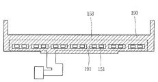
도 5는 본 발명에 따른 백라이트 유닛 조립시에 LED 기판(FPCB)과 이 LED 기판 내측에 부착된 차광테이프의 결합 구조를 개략적으로 나타낸 평면도이다.
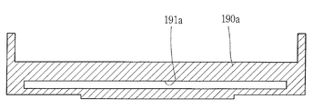
도 6은 본 발명에 따른 백라이트 유닛 조립시에 LED 기판 내측에 부착되는 차광테이프의 다른 실시 예를 도시한 차광테이프의 평면도이다.
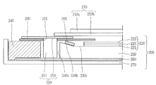
도 7은 본 발명에 따른 백라이트유닛을 구비한 액정표시장치의 다른 실시 예로서, 차광테이프와 도광판의 경사면 사이의 이격 공간부에 블랙/화이트 테이프가 부착된 상태를 도시한 결합 단면도이다.
도 8은 본 발명에 따른 백라이트유닛을 구비한 액정표시장치의 또 다른 실시 예로서, 차광테이프와 도광판의 평편한 출사면 사이의 이격 공간부에 블랙/화이트 테이프가 부착된 상태를 도시한 결합 단면도이다.1 is a cross-sectional view of a liquid crystal display having a backlight unit according to the related art.
2 is a schematic cross-sectional view of a liquid crystal display device having a backlight unit of a liquid crystal display device according to the related art, in which light leakage is generated together with the rising phenomenon of the LED FPCB.
3 is an exploded perspective view of a liquid crystal display device having a backlight unit according to the present invention.
4 is a cross-sectional view of a liquid crystal display having a backlight unit of the liquid crystal display according to the present invention.
5 is a plan view schematically illustrating a coupling structure of an LED substrate FPCB and a light shielding tape attached to an inside of the LED substrate when the backlight unit is assembled according to the present invention.
6 is a plan view of a light shielding tape showing another embodiment of a light shielding tape attached to an inside of an LED substrate at the time of assembling a backlight unit according to the present invention.
FIG. 7 is a cross-sectional view illustrating a state in which a black / white tape is attached to a spaced part between a light shielding tape and an inclined surface of a light guide plate according to another embodiment of the liquid crystal display device having the backlight unit according to the present invention.
8 is a cross-sectional view illustrating a state in which a black / white tape is attached to a spaced part between a light shielding tape and a flat exit surface of a light guide plate according to another embodiment of the liquid crystal display device having the backlight unit according to the present invention. to be.
이하 본 발명에 따른 백라이트 유닛 및 이를 구비한 액정표시장치에 대해 첨부된 도면을 참조하여 상세히 설명한다.Hereinafter, a backlight unit and a liquid crystal display device having the same according to the present invention will be described in detail with reference to the accompanying drawings.
도 3은 본 발명에 따른 백라이트 유닛를 구비한 액정표시장치의 분해 사시도이다.3 is an exploded perspective view of a liquid crystal display device having a backlight unit according to the present invention.
도 4는 본 발명에 따른 액정표시장치의 백라이트 유닛를 구비한 액정표시장치의 결합 단면도이다.4 is a cross-sectional view of a liquid crystal display having a backlight unit of the liquid crystal display according to the present invention.
본 발명에 따른 액정표시장치는, 도 3 및 4에 도시된 바와 같이, 액정패널 (110)과, 상기 액정패널(110)에 광을 공급하는 백라이트유닛(100)과, 상기 액정패널(110)과 백라이트유닛(100)을 감싸며 지지하는 가이드패널(140), 상기 가이드패널(140)과 결합되며, 상기 백라이트 유닛(100)이 수납되는 버텀 커버(170), 상기 액정패널(110)의 전면 가장자리부를 덮어 감싸는 탑 케이스(180)를 포함한다.3 and 4, the liquid crystal display according to the present invention, the
여기서, 상기 액정패널(110)은 컬러필터 어레이 기판(110a)과 TFT 어레이 기판(110b) 및 이들 사이에 개재된 액정층(미도시)을 포함한다. 또한, 도면에는 도시하지 않았지만, 상기 액정패널(110)은 액정패널(110)을 투과하는 빛이 교차 편광되도록 상기 컬러필터 어레이기판(110a)의 전면 및 TFT 어레이 기판(110b)의 배면에 각각 부착된 전면 편광판(미도시) 및 후면 편광판(미도시)을 더 포함한다. Here, the
이러한 액정패널(110)은 화소 단위를 이루는 액정 셀들이 매트릭스 형태로 배열되어 있으며, 드라이버 구동회로(113)에서 전달되는 화상 신호 정보에 따라 액정 셀들이 광 투과율을 조절함으로써 화상을 형성하게 된다. In the
상기 TFT 어레이 기판(110b)에는, 도면에는 도시하지 않았지만, 복수의 게이트 라인과 복수의 데이터 라인이 매트릭스 형태로 형성되어 있으며, 상기 게이트 라인과 데이터 라인이 교차점에는 박막트랜지스터(Thin Film Transistor; TFT)가 형성되어 있다. 드라이버 구동회로(113)에서 전달된 신호전압은 박막트랜지스터를 통해 화소전극과 후술할 컬러필터 어레이 기판(110a)의 공통전극(미도시) 사이에 인가되며, 화소전극과 공통전극 사이의 액정은 이 신호전압에 따라 정렬되어 광 투과율을 정하게 된다.Although not shown in the drawing, a plurality of gate lines and a plurality of data lines are formed in a matrix form on the
상기 컬러필터 어레이 기판(110a)에는, 도면에는 도시하지 않았지만, 블랙 매트릭스를 경계로 적색, 녹색 및 청색 또는 청록색, 자홍색 및 노랑색이 반복되어 형성되어 있는 컬러필터와 공통전극을 포함한다. 상기 공통전극은 ITO(Indium Tin Oxide) 또는 IZO(Indium Zinc Oxide) 등의 투명한 도전성 물질로 이루어진다. Although not shown in the drawing, the color
또한, 상기 액정 패널(110)의 일측에는 상기 액정패널에 형성된 단위 화소를 구동하기 위한 구동 드라이버(113)와, 상기 액정패널에 일단이 연결된 가요성 인쇄회로기판(Flexible Printed Circuit Board; FPCB, 115)이 연결되어 있다.In addition, one side of the
상기 백라이트 유닛(100)은 광을 발생하는 광원부(150)과 상기 광원부(150)에서 발생하는 광을 상기 액정패널(110)의 전면으로 제공하기 위한 도광판(130), 및 상기 도광판(130)의 배면에 부착되어 후방으로 방출되는 광을 반사시킴으로써 광의 효율을 향상시키는 반사 시트(160), 및 상기 도광판(130)의 전면에 적층되어 도광판(130)으로부터 방출되는 광을 산란시키는 다수의 광학시트(120)를 포함한다.The
여기서, 상기 광원부(150)는 냉음극 형광램프(Cothode Fluorescent Lamp: CCFL), 외부전극 형광램프(External Electrode Fluorescent Lamp: EEFL), 발광다이오드(Light Emitting Diode: LED)소자 중 어느 하나가 사용되는데, 여기서는 발광 다이오드 소자(LED소자)를 적용하는 경우를 예로 들고 있다. 또한, 상기 광원부 (150)는 LED소자(151)와, 상기 LED소자(151)가 실장된 기판(FPCB; flexible printed circuit board, 153)을 포함한다. 상기 LED소자(151)는 사이드 뷰형(side viewing type) 소자로서, 상기 LED소자(151)는 도광판(130)의 입사면(130a)을 향해 광을 출광시킨다. 또한, 상기 기판(153)은 휘어짐이 우수한 연성 인쇄회로기판으로서, 내부에 회로(미도시)가 형성되어 있어, 상기 회로를 통해 LED소자(151)에 외부 전원을 공급한다. 여기서는, 상기 광원부(150)는 도광판(130)의 일 측면에만 설치되는 경우에 대해 설명하고 있지만, 필요에 따라서는 도광판(130)의 양 측면 또는 세 측면에 설치할 수도 있다. Here, the
상기 다수의 광학시트(120)는 상기 도광판(130)으로부터 입사되는 광을 확산 및 집광하기 위한 것으로, 확산시트(121)와 프리즘시트(123) 및 보호시트(125)로 구비된다. 경우에 따라서는 두 개의 확산시트와 두 개의 프리즘 시트로 구비될 수도 있다. 이때, 상기 확산시트(121)는 베이스 판과 이 베이스 판에 형성된 구슬 모양의 코팅층으로 이루어져 있다. 상기 확산시트(121)는 광원부(150)로부터의 빛을 확산시켜 액정패널(110)로 공급하는 역할을 한다. 상기 확산시트(121)는 2장 또는 3장을 겹쳐서 사용할 수도 있다. 또한, 상기 프리즘 시트(123)는 상부면에 삼각기둥 모양의 프리즘이 일정한 배열을 갖고 형성되어 있다. 상기 프리즘 시트(123)는 확산시트(121)에서 확산된 빛을 상부의 액정패널(110)의 평면에 수직한 방향으로 집광하는 역할을 수행한다. 상기 프리즘 시트(123)는 통상 2장이 사용되며 각 프리즘 시트(123)에 형성된 마이크로 프리즘은 소정의 각도를 이루고 있다. 따라서, 상기 프리즘 시트(123)를 통과한 빛은 거의 대부분 수직하게 진행되어 균일한 휘도 분포를 제공하게 된다. 가장 상부에 위치하는 보호시트(125)는 스크래치(scratch)에 약한 프리즘 시트(123)를 보호한다.The plurality of
한편, 상기 도광판(130)은 상기 LED소자(151)의 일 측변을 따라 위치하면서 상기 액정패널(110)의 배면에 배치되어 상기 LED소자(151)에서 발생된 빛을 액정패널(110)의 배면으로 유도한다. 상기 도광판(130)은 상기 LED소자(151)로부터 빛을 받는 입사면(130a)과, 상기 입사면(130a)에서 연장되어 액정패널(110)과 대향하는 경사부(130b)를 포함한 출사면(130c)과, 상기 LED소자(151)에서 입사면(130a)으로 조사된 빛이 출사면(130c)으로 진행되도록 도트 패턴(미도시)이 형성된 배면을 갖는다. 이에 상기 도광판(130)은 도광판(130)의 일 측변을 따라, 즉 입사면(130a)에 인접하여 배치된 LED소자(151)에서 입사면(130a)으로 조사된 빛을 평면 광으로 바꾸어 출사면(130b)을 통해 상기 액정패널(110)로 균일하게 전달하게 된다. 상기 도광판(130)의 재질로는 강도가 높아 쉽게 변형되거나 깨지지 않으며 투과율이 좋은 PMMA(Polymethy- methacrylate)가 사용될 수 있다. Meanwhile, the
여기서, 상기 도광판(130)은 입사면(130b)과 접해 있는 상면에는 경사부 (130b)가 형성되어 있으며, 이 경사부(130b)를 제외한 상면 전체는 단면이 평편한 출사면(130c)으로 구성되어 있다. 한편, 상기 도광판(130)은 입사면(130b)에서 멀어질수록 점점 두께가 얇아지는 쇄기형(wedge)으로 형성되거나, 평편한 판형(plate type)으로 형성될 수도 있다. 하지만, 노트 PC나 핸드폰 등의 소형 제품에 적용되는 액정표시장치의 경우에는 쇄기형(wedge) 형상의 도광판(130)이 적용될 수 있으며, 통상적으로 두께가 두꺼운 쪽의 측벽에 광원부(150)가 구비된다. Here, the
상기 가이드 패널(140)은 상기 도광판(130)의 측면부를 감싸는 사각틀 형태로 구성되며, PC 재질과 같은 플라스틱 재질 또는 금속(metal) 재질로 형성된다. 이때, 상기 가이드 패널(140)의 상부에는 액정패널(110)과 함께 다수의 LED(151)가 실장된 LED기판(FPCB)(153)이 안착된다. 또한, 상기 가이드패널(140)과 상기 LED기판(153) 사이에는 양면 접착 특성을 가지는 차광 테이프(190)가 부착되어 있어, 상기 LED기판(153)이 상기 가이드패널(140)에 유동없이 고정된다. 이때, 상기 차광테이프(19)에는 상기 다수의 LED(151)가 들어갈 수 있도록 LED 개구부(191)들이 형성되어 있어, 상기 차광테이프(190)의 일면은 LED 개구부(191) 각각에 LED(151)가 끼워진 상태에서 LED기판(153) 안쪽 부분과 접착되고, 그 타면은 상기 가이드패널 (140)과 접착된다. 따라서, 상기 LED기판(153)에 별도의 양면 테이프를 부착할 필요가 없게 된다.The
한편, 상기 반사시트(160)는 상기 도광판(130)의 하부에 마련되며, 상기 도광판(130)의 하부로 출사되는 일부 광을 도광판(130)의 출사면(130b)으로 반사시켜 광 효율을 높여 주고, 입사광 전체의 반사량을 조절하여 출사면 전체가 균일한 휘도 분포를 가지도록 한다.On the other hand, the
또한, 상기 버텀커버(170)는 상부가 개방된 장방형 박스 형상으로 구성되어 있는데, 이 버텀커버(170) 내에는 상기 가이드패널(140)에 의해 감싸지는 도광판 (130)과 반사시트(160)를 포함한 백라이트 유닛(100)의 구성요소들이 수납된다. In addition, the
따라서, 상기 액정패널(110)과 백라이트유닛(100)이 수납된 버텀커버(170)는 상기 액정패널(110)의 상면 가장자리부와 가이드패널(140)의 측면을 감싸는 탑 케이스(180)와 결합되어져, 액정표시장치를 이루게 된다.Therefore, the
상기 구성으로 이루어진 본 발명에 따른 백라이트 유닛은 도광판이 적용된 에지형(Edge type) 백라이트유닛에 적용한 것이지만, 도광판 대신에 플레이트를 사용하는 직하형(Director type) 백라이트유닛에도 동일하게 적용가능하다. The backlight unit according to the present invention having the above configuration is applied to an edge type backlight unit to which a light guide plate is applied, but may be equally applicable to a direct type backlight unit using a plate instead of a light guide plate.
한편, 이와 같은 구성으로 이루어진 본 발명에 따른 백라이트 유닛을 구비한 액정표시장치의 조립 과정에 대해 도 3 내지 도 6을 참조하여 설명하면 다음과 같다.Meanwhile, a process of assembling the liquid crystal display device having the backlight unit according to the present invention having the above configuration will be described with reference to FIGS. 3 to 6.
도 5는 본 발명에 따른 백라이트 유닛 조립시에 LED 기판(FPCB)과 이 LED 기판 내측에 부착된 차광테이프의 결합 구조를 개략적으로 나타낸 평면도이다.5 is a plan view schematically illustrating a coupling structure of an LED substrate FPCB and a light shielding tape attached to an inside of the LED substrate when the backlight unit is assembled according to the present invention.
도 6은 본 발명에 따른 백라이트 유닛 조립시에 LED 기판 내측에 부착되는 차광테이프의 다른 실시 예를 도시한 차광테이프의 평면도이다.6 is a plan view of a light shielding tape showing another embodiment of a light shielding tape attached to an inside of an LED substrate at the time of assembling a backlight unit according to the present invention.
도 3 및 4에 도시된 바와 같이, 바텀커버(170)의 내측 저면에 백라이트 유닛 (100)의 반사시트(160)가 안착되고, 상기 반사시트(160) 상에 도광판(130)과 광학시트(120)가 배치되는데, 이들 도광판(130) 및 광학시트(120)는 가이드 패널(140)에 의해 감싸지게 된다. As shown in FIGS. 3 and 4, the
이후, 상기 도광판(130)의 일측면과 가이드 패널(140) 사이에 광원부(150)가 배치된다. 이때, 상기 광원부(150)의 다수의 LED(151)는 상기 도광판(130)의 입사면(130)에 인접되게 배치되며, 이 다수의 LED(151)가 실장된 LED기판(153)은 상기 가이드패널(140)의 상면과 상기 도광판(130)의 상부에 배치된다. Thereafter, the
그 다음, 도 4 및 5에 도시된 바와 같이, 상기 가이드패널(140)과 상기 LED기판(153) 사이에는 양면 접착 특성을 가지는 차광 테이프(190)가 부착된다. 이때, 상기 차광테이프(19)에는, 도 5에 도시된 바와 같이, 상기 다수의 LED(151)가 들어갈 수 있도록 일정 간격을 두고 다수의 LED 개구부(191)들이 형성되어 있어, 상기 LED 개구부(191) 각각에 LED(151)가 끼워진 상태에서 상기 차광테이프(190)의 일면은 상기 LED기판(153) 안쪽 부분과 접착되고, 그 타면은 상기 가이드패널(140)과 접착된다. 또한, 상기 차광테이프(190)는 백라이트 유닛의 조립시에 LED기판(153)을 고정하는 역할과 함께 광학시트(120)와 가이드 패널(140) 사이에서 방출되는 빛을 차광하여 액정표시패널(110)의 가장자리부에서 원치 않는 빛샘 현상을 예방하는 역할을 겸한다.Next, as illustrated in FIGS. 4 and 5, a
한편, 차광테이프의 다른 실시 예로서, 도 6에 도시된 바와 같이, 차광테이프(190a)에는, 상기 다수의 LED(151)가 들어갈 수 있을 정도의 LED 개구부(191a)가 형성되어 있어, 상기 LED 개구부(191)에 다수의 LED(151)가 끼워진 상태에서 상기 차광테이프(190a)의 일면은 상기 LED기판(153) 안쪽 부분과 접착되고, 그 타면은 상기 가이드패널(140)과 접착되도록 조립할 수도 있다. On the other hand, as another embodiment of the light shielding tape, as shown in Figure 6, the
이렇게 하여, 상기 LED기판(153)은 상기 가이드패널(140)에 유동없이 고정되게 된다. 이때, 상기 LED기판(153)은 상기 차광테이프(190)에 의해 상기 가이드패널(140) 상면에 접착되어 고정되기 때문에, 상기 LED기판(153)을 고정시켜 주기 위한 별도의 양면 테이프를 부착할 필요가 없게 된다.In this way, the
이어서, 상기 LED기판(153)을 포함한 상기 가이드패널(140) 상면에 액정패널 (110)을 배치하고, 상기 액정패널(110)의 상면 가장자리부, 즉 비 표시지역과 상기 가이드패널(140)의 측면부를 감싸도록 탑케이스(180)를 조립함으로써 백라이트유닛을 구비한 액정표시장치 조립 공정을 완료하게 된다. Subsequently, the
한편, 본 발명의 다른 실시 예들에 따른 백라이트유닛을 구비한 액정표시장치에 대해 도 7을 참조하여 설명하면 다음과 같다. 여기서는 차광테이프와 광학시트 사이에 생기는 갭을 줄이기 위해 블랙/화이트 테이프가 추가로 부착되는 경우에 대한 실시 예이다.Meanwhile, a liquid crystal display device having a backlight unit according to other embodiments of the present invention will be described with reference to FIG. 7. In this case, the black / white tape is additionally attached to reduce the gap between the light shielding tape and the optical sheet.
도 7은 본 발명에 따른 백라이트유닛을 구비한 액정표시장치의 다른 실시 예로서, 차광테이프와 도광판의 경사면 사이의 이격 공간부에 블랙/화이트 테이프가 부착된 상태를 도시한 결합 단면도이다.FIG. 7 is a cross-sectional view illustrating a state in which a black / white tape is attached to a spaced part between a light shielding tape and an inclined surface of a light guide plate according to another embodiment of the liquid crystal display device having the backlight unit according to the present invention.
본 발명에 따른 백라이트유닛을 구비한 액정표시장치는, 도 7에 도시된 바와 같이, 액정패널(210)과, 상기 액정패널(210)에 광을 공급하는 백라이트유닛(200)과, 상기 액정패널 (210)과 백라이트유닛(200)을 감싸며 지지하는 가이드패널 (240), 상기 가이드패널 (240)과 결합되며, 상기 백라이트 유닛(200)이 수납되는 버텀 커버 (270), 상기 액정패널(210)의 전면 가장자리부를 덮어 감싸는 탑 케이스 (미도시)를 포함한다.As shown in FIG. 7, a liquid crystal display device having a backlight unit according to the present invention includes a
여기서, 상기 액정패널(210)은 컬러필터 어레이 기판(210a)과 TFT 어레이 기판(210b) 및 이들 사이에 개재된 액정층(미도시)을 포함한다. 또한, 도면에는 도시하지 않았지만, 상기 액정패널(210)은 액정패널(210)을 투과하는 빛이 교차 편광되도록 상기 컬러필터 어레이기판(210a)의 전면 및 TFT 어레이 기판(210b)의 배면에 각각 부착된 전면 편광판(미도시) 및 후면 편광판(미도시)을 더 포함한다. Here, the
이러한 액정패널(210)은 화소 단위를 이루는 액정 셀들이 매트릭스 형태로 배열되어 있으며, 드라이버 구동회로(미도시)에서 전달되는 화상 신호 정보에 따라 액정 셀들이 광 투과율을 조절함으로써 화상을 형성하게 된다. In the
상기 TFT 어레이 기판(210b)에는, 도면에는 도시하지 않았지만, 복수의 게이트 라인과 복수의 데이터 라인이 매트릭스 형태로 형성되어 있으며, 상기 게이트 라인과 데이터 라인이 교차점에는 박막트랜지스터(Thin Film Transistor; TFT)가 형성되어 있다. 드라이버 구동회로(미도시)에서 전달된 신호전압은 박막트랜지스터를 통해 화소전극과 후술할 컬러필터 어레이 기판(210a)의 공통전극(미도시) 사이에 인가되며, 화소전극과 공통전극 사이의 액정은 이 신호전압에 따라 정렬되어 광 투과율을 정하게 된다.Although not shown in the figure, a plurality of gate lines and a plurality of data lines are formed in a matrix form on the
상기 컬러필터 어레이 기판(210a)에는, 도면에는 도시하지 않았지만, 블랙 매트릭스를 경계로 적색, 녹색 및 청색 또는 청록색, 자홍색 및 노랑색이 반복되어 형성되어 있는 컬러필터와 공통전극을 포함한다. 상기 공통전극은 ITO(Indium Tin Oxide) 또는 IZO(Indium Zinc Oxide) 등의 투명한 도전성 물질로 이루어진다. Although not shown in the drawing, the color
또한, 도면에는 도시하지 않았지만, 본 발명의 일 실시 예와 마찬가지로, 상기 액정 패널(210)의 일측에는 상기 액정패널에 형성된 단위 화소를 구동하기 위한 구동 드라이버(미도시)와, 상기 액정패널에 일단이 연결된 가요성 인쇄회로기판 (Flexible Printed Circuit Board; FPCB, 미도시)이 연결되어 있다.In addition, although not shown in the drawing, as in the exemplary embodiment of the present invention, one side of the
상기 백라이트 유닛(200)은 광을 발생하는 광원부(250)과 상기 광원부(250)에서 발생하는 광을 상기 액정패널(210)의 전면으로 제공하기 위한 도광판(230), 및 상기 도광판(230)의 배면에 부착되어 후방으로 방출되는 광을 반사시킴으로써 광의 효율을 향상시키는 반사 시트(260), 및 상기 도광판(230)의 전면에 적층되어 도광판(230)으로부터 방출되는 광을 산란시키는 다수의 광학시트(220)를 포함한다.The
여기서, 상기 광원부(250)는 LED소자(251)와, 상기 LED소자(251)가 실장된 기판(FPCB; flexible printed circuit board, 253)을 포함한다. 상기 LED소자(251)는 사이드 뷰형(side viewing type) 소자로서, 상기 LED소자(251)는 도광판(230)의 입사면(230a)을 향해 광을 출광시킨다. 또한, 상기 기판(253)은 휘어짐이 우수한 연성 인쇄회로기판으로서, 내부에 회로(미도시)가 형성되어 있어, 상기 회로를 통해 LED소자(251)에 외부 전원을 공급한다. 여기서는, 상기 광원부(250)는 도광판 (230)의 일 측면에만 설치되는 경우에 대해 설명하고 있지만, 필요에 따라서는 도광판(230)의 양 측면 또는 세 측면에 설치할 수도 있다. The
상기 다수의 광학시트(220)는 상기 도광판(330)으로부터 입사되는 광을 확산 및 집광하기 위한 것으로, 확산시트(221)와 프리즘시트(223) 및 보호시트(225)로 구비된다. 경우에 따라서는 두 개의 확산시트와 두 개의 프리즘 시트로 구비될 수도 있다. 이때, 상기 확산시트(221)는 베이스 판과 이 베이스 판에 형성된 구슬 모양의 코팅층으로 이루어져 있다. 상기 확산시트(221)는 광원부(250)로부터의 빛을 확산시켜 액정패널(210)로 공급하는 역할을 한다. 상기 확산시트(221)는 2장 또는 3장을 겹쳐서 사용할 수도 있다. 또한, 상기 프리즘 시트(223)는 상부면에 삼각기둥 모양의 프리즘이 일정한 배열을 갖고 형성되어 있다. 상기 프리즘 시트(223)는 확산시트(221)에서 확산된 빛을 상부의 액정패널(210)의 평면에 수직한 방향으로 집광하는 역할을 수행한다. 상기 프리즘 시트(223)는 통상 2장이 사용되며 각 프리즘 시트(223)에 형성된 마이크로 프리즘은 소정의 각도를 이루고 있다. 따라서, 상기 프리즘 시트(223)를 통과한 빛은 거의 대부분 수직하게 진행되어 균일한 휘도 분포를 제공하게 된다. 가장 상부에 위치하는 보호시트(225)는 스크래치(scratch)에 약한 프리즘 시트(223)를 보호한다.The plurality of
한편, 상기 도광판(230)은 상기 LED소자(251)의 일 측변을 따라 위치하면서 상기 액정패널(210)의 배면에 배치되어 상기 LED소자(251)에서 발생된 빛을 액정패널(210)의 배면으로 유도한다. 상기 도광판(230)은 상기 LED소자(251)로부터 빛을 받는 입사면(230a)과, 상기 입사면(230a)에서 연장되어 액정패널(210)과 대향하는 경사부(230b)를 포함한 출사면(230c)과, 상기 LED소자(251)에서 입사면(230a)으로 조사된 빛이 출사면(230c)으로 진행되도록 도트 패턴(미도시)이 형성된 배면을 갖는다. 이에 상기 도광판(230)은 도광판(230)의 일 측변을 따라, 즉 입사면(230a)에 인접하여 배치된 LED소자(251)에서 입사면(230a)으로 조사된 빛을 평면 광으로 바꾸어 출사면(230b)을 통해 상기 액정패널(210)로 균일하게 전달하게 된다. Meanwhile, the
여기서, 상기 도광판(230)은 입사면(230b)과 접해 있는 상면에는 경사부 (230b)가 형성되어 있으며, 이 경사부(230b)를 제외한 상면 전체는 단면이 평편한 출사면(230c)으로 구성되어 있다. 한편, 상기 도광판(230)은 입사면(230b)에서 멀어질수록 점점 두께가 얇아지는 쇄기형(wedge)으로 형성되거나, 평편한 판형(plate type)으로 형성될 수도 있다. Here, the
상기 가이드 패널(240)은 상기 도광판(230)의 측면부를 감싸는 사각틀 형태로 구성되며, PC 재질과 같은 플라스틱 재질 또는 금속(metal) 재질로 형성된다. 이때, 상기 가이드 패널(240)의 상부에는 액정패널(210)과 함께 다수의 LED(251)가 실장된 LED기판(FPCB)(253)이 안착된다. 또한, 상기 가이드패널(240)과 상기 LED기판(253) 사이에는 양면 접착 특성을 가지는 차광 테이프(290)가 부착되어 있어, 상기 LED기판(253)이 상기 가이드패널(240)에 유동없이 고정된다. 이때, 상기 차광테이프(290)에는 상기 다수의 LED(251)가 들어갈 수 있도록 LED 개구부(291)들이 형성되어 있어, 상기 차광테이프(290)의 일면은 LED 개구부(291) 각각에 LED(251)가 끼워진 상태에서 LED기판(253) 안쪽 부분과 접착되고, 그 타면은 상기 가이드패널 (240)과 접착된다. 따라서, 상기 LED기판(253)에 별도의 양면 테이프를 부착할 필요가 없게 된다.The
또한, 상기 차광테이프(290)와 광학시트(220) 사이에는 갭(293)이 형성될 수 있는데, 이러한 갭(293)을 줄여 주기 위해, 상기 도광판(230)의 상부, 즉 경사부 (230b) 표면에 블랙/화이트 테이프(295)를 부착한다. 이때, 상기 블랙/화이트 테이프(295)가 상기 도광판(230)의 경사부(230b)에 부착됨으로써, 차광테이프 (290)와 광학시트(220) 간의 갭(293)이 줄어 들어, 기존에 LED기판을 도광판에 밀착하여 조립함으로써 생기는 LED기판의 뜸으로 인해 발생되는 빛샘을 최대한 방지할 수 있게 된다. In addition, a gap 293 may be formed between the
한편, 상기 반사시트(260)는 상기 도광판(230)의 하부에 마련되며, 상기 도광판(230)의 하부로 출사되는 일부 광을 도광판(230)의 출사면(230b)으로 반사시켜 광 효율을 높여 주고, 입사광 전체의 반사량을 조절하여 출사면 전체가 균일한 휘도 분포를 가지도록 한다.On the other hand, the
또한, 상기 버텀커버(270)는 상부가 개방된 장방형 박스 형상으로 구성되어 있는데, 이 버텀커버(270) 내에는 상기 가이드패널(240)에 의해 감싸지는 도광판 (230)과 반사시트(260)를 포함한 백라이트 유닛(200)의 구성요소들이 수납된다. In addition, the
따라서, 상기 액정패널(210)과 백라이트유닛(200)이 수납된 버텀커버(270)는 상기 액정패널(210)의 상면 가장자리부와 가이드패널(240)의 측면을 감싸는 탑 케이스(미도시)와 결합되어져, 액정표시장치를 이루게 된다.Accordingly, the
한편, 본 발명의 또 다른 실시 예들에 따른 백라이트유닛을 구비한 액정표시장치에 대해 도 8을 참조하여 설명하면 다음과 같다. 여기서는 차광테이프와 광학시트 사이에 생기는 갭을 줄이기 위해 블랙/화이트 테이프가 추가로 부착되는 경우에 대한 다른 실시 예이다.Meanwhile, a liquid crystal display device having a backlight unit according to still another embodiment of the present invention will be described with reference to FIG. 8. Here, another embodiment of the case where the black / white tape is additionally attached to reduce the gap between the light-shielding tape and the optical sheet.
도 8은 본 발명에 따른 백라이트유닛을 구비한 액정표시장치의 또 다른 실시 예로서, 차광테이프와 도광판의 평편한 출사면 사이의 이격 공간부에 블랙/화이트 테이프가 부착된 상태를 도시한 결합 단면도이다.8 is a cross-sectional view illustrating a state in which a black / white tape is attached to a spaced part between a light shielding tape and a flat exit surface of a light guide plate according to another embodiment of the liquid crystal display device having the backlight unit according to the present invention. to be.
본 발명에 따른 백라이트유닛을 구비한 액정표시장치는, 도 8에 도시된 바와 같이, 액정패널(310)과, 상기 액정패널(310)에 광을 공급하는 백라이트유닛(300)과, 상기 액정패널 (310)과 백라이트유닛(300)을 감싸며 지지하는 가이드패널 (340), 상기 가이드패널 (340)과 결합되며, 상기 백라이트 유닛(300)이 수납되는 버텀 커버(370), 상기 액정패널(310)의 전면 가장자리부를 덮어 감싸는 탑 케이스(미도시)를 포함한다.As shown in FIG. 8, the liquid crystal display device having the backlight unit according to the present invention includes a
여기서, 상기 액정패널(310)은 컬러필터 어레이 기판(310a)과 TFT 어레이 기판(310b) 및 이들 사이에 개재된 액정층(미도시)을 포함한다. 또한, 도면에는 도시하지 않았지만, 상기 액정패널(310)은 액정패널(310)을 투과하는 빛이 교차 편광되도록 상기 컬러필터 어레이기판(310a)의 전면 및 TFT 어레이 기판(310b)의 배면에 각각 부착된 전면 편광판(미도시) 및 후면 편광판(미도시)을 더 포함한다. Here, the
이러한 액정패널(310)은 화소 단위를 이루는 액정 셀들이 매트릭스 형태로 배열되어 있으며, 드라이버 구동회로(미도시)에서 전달되는 화상 신호 정보에 따라 액정 셀들이 광 투과율을 조절함으로써 화상을 형성하게 된다. In the
상기 TFT 어레이 기판(310b)에는, 도면에는 도시하지 않았지만, 복수의 게이트 라인과 복수의 데이터 라인이 매트릭스 형태로 형성되어 있으며, 상기 게이트 라인과 데이터 라인이 교차점에는 박막트랜지스터(Thin Film Transistor; TFT)가 형성되어 있다. 드라이버 구동회로(미도시)에서 전달된 신호전압은 박막트랜지스터를 통해 화소전극과 후술할 컬러필터 어레이 기판(310a)의 공통전극(미도시) 사이에 인가되며, 화소전극과 공통전극 사이의 액정은 이 신호전압에 따라 정렬되어 광 투과율을 정하게 된다.Although not shown in the figure, a plurality of gate lines and a plurality of data lines are formed in a matrix form on the
상기 컬러필터 어레이 기판(310a)에는, 도면에는 도시하지 않았지만, 블랙 매트릭스를 경계로 적색, 녹색 및 청색 또는 청록색, 자홍색 및 노랑색이 반복되어 형성되어 있는 컬러필터와 공통전극을 포함한다. 상기 공통전극은 ITO(Indium Tin Oxide) 또는 IZO(Indium Zinc Oxide) 등의 투명한 도전성 물질로 이루어진다. Although not shown in the drawing, the color
또한, 도면에는 도시하지 않았지만, 본 발명의 일 실시 예와 마찬가지로, 상기 액정 패널(310)의 일측에는 상기 액정패널에 형성된 단위 화소를 구동하기 위한 구동 드라이버(미도시)와, 상기 액정패널에 일단이 연결된 가요성 인쇄회로기판 (Flexible Printed Circuit Board; FPCB, 미도시)이 연결되어 있다.In addition, although not shown in the drawing, as in the exemplary embodiment of the present invention, one side of the
상기 백라이트 유닛(300)은 광을 발생하는 광원부(350)과 상기 광원부(350)에서 발생하는 광을 상기 액정패널(310)의 전면으로 제공하기 위한 도광판(330), 및 상기 도광판(330)의 배면에 부착되어 후방으로 방출되는 광을 반사시킴으로써 광의 효율을 향상시키는 반사 시트(360), 및 상기 도광판(330)의 전면에 적층되어 도광판(330)으로부터 방출되는 광을 산란시키는 다수의 광학시트(320)를 포함한다.The
여기서, 상기 광원부(350)는 LED소자(351)와, 상기 LED소자(351)가 실장된 기판(FPCB; flexible printed circuit board, 353)을 포함한다. 상기 LED소자(351)는 사이드 뷰형(side viewing type) 소자로서, 상기 LED소자(351)는 도광판(330)의 입사면(330a)을 향해 광을 출광시킨다. 또한, 상기 기판(353)은 휘어짐이 우수한 연성 인쇄회로기판으로서, 내부에 회로(미도시)가 형성되어 있어, 상기 회로를 통해 LED소자(351)에 외부 전원을 공급한다. 여기서는, 상기 광원부(350)는 도광판 (330)의 일 측면에만 설치되는 경우에 대해 설명하고 있지만, 필요에 따라서는 도광판(330)의 양 측면 또는 세 측면에 설치할 수도 있다. The
상기 다수의 광학시트(320)는 상기 도광판(330)으로부터 입사되는 광을 확산 및 집광하기 위한 것으로, 확산시트(321)와 프리즘시트(323) 및 보호시트(325)로 구비된다. 경우에 따라서는 두 개의 확산시트와 두 개의 프리즘 시트로 구비될 수도 있다. 이때, 상기 확산시트(321)는 베이스 판과 이 베이스 판에 형성된 구슬 모양의 코팅층으로 이루어져 있다. 상기 확산시트(321)는 광원부(350)로부터의 빛을 확산시켜 액정패널(310)로 공급하는 역할을 한다. 상기 확산시트(321)는 2장 또는 3장을 겹쳐서 사용할 수도 있다. 또한, 상기 프리즘 시트(323)는 상부면에 삼각기둥 모양의 프리즘이 일정한 배열을 갖고 형성되어 있다. 상기 프리즘 시트(323)는 확산시트(321)에서 확산된 빛을 상부의 액정패널(310)의 평면에 수직한 방향으로 집광하는 역할을 수행한다. 상기 프리즘 시트(323)는 통상 2장이 사용되며 각 프리즘 시트(323)에 형성된 마이크로 프리즘은 소정의 각도를 이루고 있다. 따라서, 상기 프리즘 시트(323)를 통과한 빛은 거의 대부분 수직하게 진행되어 균일한 휘도 분포를 제공하게 된다. 가장 상부에 위치하는 보호시트(325)는 스크래치(scratch)에 약한 프리즘 시트(323)를 보호한다.The plurality of
한편, 상기 도광판(330)은 상기 LED소자(351)의 일 측변을 따라 위치하면서 상기 액정패널(310)의 배면에 배치되어 상기 LED소자(351)에서 발생된 빛을 액정패널(310)의 배면으로 유도한다. 상기 도광판(330)은 상기 LED소자(351)로부터 빛을 받는 입사면(330a)과, 상기 입사면(330a)에서 연장되어 액정패널(310)과 대향하는 경사부(330b)를 포함한 출사면(330c)과, 상기 LED소자(351)에서 입사면(330a)으로 조사된 빛이 출사면(330c)으로 진행되도록 도트 패턴(미도시)이 형성된 배면을 갖는다. 이에 상기 도광판(330)은 도광판(330)의 일 측변을 따라, 즉 입사면(330a)에 인접하여 배치된 LED소자(351)에서 입사면(330a)으로 조사된 빛을 평면 광으로 바꾸어 출사면(330b)을 통해 상기 액정패널(310)로 균일하게 전달하게 된다. On the other hand, the
여기서, 상기 도광판(330)은 입사면(330b)과 접해 있는 상면에는 경사부 (330b)가 형성되어 있으며, 이 경사부(330b)를 제외한 상면 전체는 단면이 평편한 출사면(330c)으로 구성되어 있다. 한편, 상기 도광판(330)은 입사면(330b)에서 멀어질수록 점점 두께가 얇아지는 쇄기형(wedge)으로 형성되거나, 평편한 판형(plate type)으로 형성될 수도 있다. Here, the
상기 가이드 패널(340)은 상기 도광판(330)의 측면부를 감싸는 사각틀 형태로 구성되며, PC 재질과 같은 플라스틱 재질 또는 금속(metal) 재질로 형성된다. 이때, 상기 가이드 패널(340)의 상부에는 액정패널(310)과 함께 다수의 LED(351)가 실장된 LED기판(FPCB)(353)이 안착된다. 또한, 상기 가이드패널(340)과 상기 LED기판(353) 사이에는 양면 접착 특성을 가지는 차광 테이프(390)가 부착되어 있어, 상기 LED기판(353)이 상기 가이드패널(340)에 유동없이 고정된다. 이때, 상기 차광테이프(390)에는 상기 다수의 LED(351)가 들어갈 수 있도록 LED 개구부(391)들이 형성되어 있어, 상기 차광테이프(390)의 일면은 LED 개구부(391) 각각에 LED(351)가 끼워진 상태에서 LED기판(353) 안쪽 부분과 접착되고, 그 타면은 상기 가이드패널 (340)과 접착된다. 따라서, 상기 LED기판(353)에 별도의 양면 테이프를 부착할 필요가 없게 된다.The
또한, 상기 차광테이프(390)와 광학시트(320) 사이에 갭(393)이 형성될 수 있는데, 이러한 갭(393)을 줄여 주기 위해, 상기 갭(393)에 위치하는 차광테이프 (390)의 배면에 블랙/화이트 테이프(395)를 부착한다. 이때, 상기 블랙/화이트 테이프(395)가 상기 차광테이프(390)의 배면에 부착됨으로써, 차광테이프(390)와 광학시트(320) 간의 갭(393)이 줄어들어, 기존에 LED기판을 도광판에 밀착하여 조립함으로써 생기는 LED기판의 뜸으로 인해 발생되는 빛샘을 최대한 방지할 수 있게 된다. In addition, a gap 393 may be formed between the
한편, 상기 반사시트(360)는 상기 도광판(330)의 하부에 마련되며, 상기 도광판(330)의 하부로 출사되는 일부 광을 도광판(330)의 출사면(330b)으로 반사시켜 광 효율을 높여 주고, 입사광 전체의 반사량을 조절하여 출사면 전체가 균일한 휘도 분포를 가지도록 한다.On the other hand, the
또한, 상기 버텀커버(370)는 상부가 개방된 장방형 박스 형상으로 구성되어 있는데, 이 버텀커버(370) 내에는 상기 가이드패널(340)에 의해 감싸지는 도광판 (330)과 반사시트(360)를 포함한 백라이트 유닛(300)의 구성요소들이 수납된다. In addition, the
따라서, 상기 액정패널(310)과 백라이트유닛(300)이 수납된 버텀커버(370)는 상기 액정패널(310)의 상면 가장자리부와 가이드패널(340)의 측면을 감싸는 탑 케이스(미도시)와 결합되어져, 액정표시장치를 이루게 된다.Accordingly, the
이상에서와 같이, 본 발명에 따르면, 백라이트 유닛 조립시에 차광테이프를 먼저 가이드패널 상면에 부착한 상태에서 LED기판을 부착하여 조립하기 때문에 LED 기판을 고정하기 위한 별도의 양면 테이프를 사용할 필요가 없다. 즉, 차광테이프에 LED가 끼워질 수 있도록 다수의 LED개구부가 형성되어 있고, 상기 차광테이프가 양면 접착 특성을 가지고 있기 때문에 별도의 LED기판에 별도의 양면 테이프를 부착할 필요가 없게 된다.As described above, according to the present invention, it is not necessary to use a separate double-sided tape for fixing the LED substrate because the LED substrate is attached and assembled while the shading tape is first attached to the upper surface of the guide panel when assembling the backlight unit. . That is, a plurality of LED openings are formed to allow the LED to be fitted to the shading tape, and since the shading tape has double-sided adhesive property, it is not necessary to attach a separate double-sided tape to a separate LED substrate.
또한, 본 발명에 따르면, LED기판에 구동을 위한 배선만 형성되는 영역에서 LED기판의 사이즈를 최소화시킬 수 있어 재료비를 절감할 수 있다. In addition, according to the present invention, it is possible to minimize the size of the LED substrate in the region where only wiring for driving is formed on the LED substrate can reduce the material cost.
그리고, 본 발명에 따르면, LED기판을 가장 마지막으로 조립할 수 있어, 재료비 절감이 가능하고, 백라이트유닛의 종류에 따라 전 라인의 자동화 조립도 가능하게 된다. 즉, 삽입(insert) 타입의 백라이트유닛의 경우 LED기판 조립시에 사람의 손이 아닌 자동화 장비로 조립이 가능해진다. In addition, according to the present invention, the LED substrate can be assembled at the end, thereby reducing material costs, and enabling automated assembly of all lines according to the type of backlight unit. That is, in the case of the insert type backlight unit, assembling is possible with automation equipment instead of human hands when assembling the LED substrate.
더욱이, 본 발명에 따르면, 차광테이프와 광학시트 사이에 발생되는 갭을 블랙/화이트 테이프를 이용하여 줄여 줌으로써, 기존에 LED기판을 도광판에 밀착하여 조립함으로써 생기는 LED기판의 뜸으로 인해 발생되는 빛샘을 방지할 수 있다. 특히, 상기 블랙/화이트 테이프를 갭이 형성되는 차광테이프 하면에 부착하거나, 도광판의 경사부에 부착함으로써 차광테이프와 광학시트 간의 갭을 줄일 수 있어, 기존에 LED기판을 도광판에 밀착하여 조립함으로써 생기는 LED기판의 뜸으로 인해 발생되는 빛샘을 최대한 방지할 수 있다. Further, according to the present invention, by reducing the gap generated between the light-shielding tape and the optical sheet using a black / white tape, the light leakage caused by the moxibustion of the LED substrate generated by assembling the LED substrate to the light guide plate in the past. It can prevent. In particular, by attaching the black / white tape to the bottom surface of the light shielding tape where the gap is formed or by attaching the black / white tape to the inclined portion of the light guide plate, the gap between the light shielding tape and the optical sheet can be reduced. It is possible to prevent the light leakage caused by the moxibustion of the LED substrate as much as possible.
이상 첨부된 도면을 참조하여 본 발명의 실시 예를 설명하였지만, 본 발명이 속하는 기술분야에서 통상의 지식을 가진 자는 본 발명이 그 기술적 사상이나 필수적인 특징을 변경하지 않고서 다른 구체적인 형태로 실시될 수 있다는 것을 이해할 수 있을 것이다. Although embodiments of the present invention have been described above with reference to the accompanying drawings, those skilled in the art to which the present invention pertains may implement the present invention in other specific forms without changing the technical spirit or essential features thereof. I can understand that.
따라서, 이상에서 기술한 실시 예들은 본 발명이 속하는 기술분야에서 통상의 지식을 가진 자에게 발명의 범주를 완전하게 알려 주기 위해 제공되는 것이므로, 모든 면에서 예시적인 것이며 한정적이 아닌 것으로 이해해야만 하며, 본 발명은 청구항의 범주에 의해 정의될 뿐이다.Therefore, since the embodiments described above are provided to completely inform the scope of the invention to those skilled in the art to which the present invention pertains, it should be understood that they are exemplary in all respects and not limited. The invention is only defined by the scope of the claims.
100: 백라이트 유닛 110: 액정패널
110a: 칼라필터 어레이기판 110b: TFT 어레이기판
113: 구동 드라이버 115: 인쇄회로기판
120: 광학시트 121: 확산시트
123: 프리즘시트 125: 보호시트
130: 도광판 130a: 입사면
130b: 경사부 130c: 출사면 140: 가이드패널 150: 광원부 151: LED 153: LED 기판(FPCB) 160: 반사시트 170: 버텀 커버
180: 탑 케이스 190: 차광테이프
191: LED개구부 193: 갭100: backlight unit 110: liquid crystal panel
110a: color
113: drive driver 115: printed circuit board
120: optical sheet 121: diffusion sheet
123: prism sheet 125: protective sheet
130:
130b:
180: top case 190: shading tape
191: LED opening 193: gap
Claims (15)
상기 광원부의 측부에 위치하며, 상기 광원으로부터 입사되는 광을 평면 광으로 변환하여 상기 액정패널 측으로 진행시키는 도광판;
상기 도광판의 측면부와 상기 광원부를 감싸는 가이드 패널;
상기 다수의 LED가 끼워지며 상기 LED기판과 상기 가이드패널에 부착된 차광테이프; 및
상기 도광판 상에 배치되는 광학시트를 포함하여 구성되는 백라이트 유닛.A light source unit including a plurality of LEDs providing light to the liquid crystal panel and an LED substrate (FPCB) on which the plurality of LEDs are mounted;
A light guide plate positioned at a side of the light source unit and configured to convert light incident from the light source into planar light and propagate it toward the liquid crystal panel;
A guide panel surrounding a side portion of the light guide plate and the light source;
A light shielding tape fitted to the plurality of LEDs and attached to the LED substrate and the guide panel; And
And a optical sheet disposed on the light guide plate.
상기 액정패널에 광을 제공하는 다수의 LED와, 이 다수의 LED가 실장되는 LED기판(FPCB)으로 구성된 광원부;
상기 광원부의 측부에 위치하며, 상기 광원으로부터 입사되는 광을 평면 광으로 변환하여 상기 액정패널 측으로 진행시키는 도광판;
상기 도광판의 측면부와 상기 광원부를 감싸는 가이드 패널;
상기 다수의 LED가 끼워지며 상기 LED기판과 상기 가이드패널에 부착된 차광테이프; 및
상기 도광판 상에 배치되는 광학시트를 포함하여 구성되는 백라이트 유닛을 구비한 액정표시장치.A liquid crystal panel;
A light source unit including a plurality of LEDs providing light to the liquid crystal panel and an LED substrate (FPCB) on which the plurality of LEDs are mounted;
A light guide plate positioned at a side of the light source unit and configured to convert light incident from the light source into planar light and propagate it toward the liquid crystal panel;
A guide panel surrounding a side portion of the light guide plate and the light source;
A light shielding tape fitted to the plurality of LEDs and attached to the LED substrate and the guide panel; And
And a backlight unit including an optical sheet disposed on the light guide plate.
액정패널에 광을 제공하는 다수의 LED와, 이 다수의 LED가 실장되는 LED기판(FPCB)으로 구성된 광원부을 제공하는 단계;
상기 가이드패널 내에 위치하며, 광원으로부터 입사되는 광을 평면 광으로 변환하여 액정패널 측으로 진행시키는 도광판을 배치하는 단계;
상기 가이드패널 내에서 상기 도광판의 일측면에 대응되게 배치되며, 액정패널에 광을 제공하는 다수의 LED와, 이 다수의 LED가 실장되는 LED기판(FPCB)으로 구성된 광원부을 제공하는 단계;
상기 다수의 LED가 끼워지도록 상기 LED기판 하면에 차광테이프를 부착하는 단계; 및
상기 차광테이프가 부착된 상기 LED기판을 상기 가이드패널 상에 위치시켜 상기 차광테이프에 의해 상기 LED기판을 상기 가이드패널에 부착시키는 단계를 포함하여 구성되는 백라이트 유닛 조립방법.Providing a guide panel having a rectangular frame shape;
Providing a light source unit including a plurality of LEDs providing light to the liquid crystal panel and an LED substrate (FPCB) on which the plurality of LEDs are mounted;
Disposing a light guide plate positioned in the guide panel and converting light incident from a light source into planar light and traveling toward the liquid crystal panel;
Providing a light source unit disposed in the guide panel corresponding to one side of the light guide plate, the light source unit including a plurality of LEDs providing light to the liquid crystal panel and an LED substrate (FPCB) on which the plurality of LEDs are mounted;
Attaching a light shielding tape to a lower surface of the LED substrate to insert the plurality of LEDs; And
Positioning the LED substrate having the light shielding tape on the guide panel, and attaching the LED substrate to the guide panel by the light shielding tape.
Priority Applications (1)
| Application Number | Priority Date | Filing Date | Title |
|---|---|---|---|
| KR1020100128670A KR20120067205A (en) | 2010-12-15 | 2010-12-15 | Backlight unit, liquid crystal display device and method assembling thereof |
Applications Claiming Priority (1)
| Application Number | Priority Date | Filing Date | Title |
|---|---|---|---|
| KR1020100128670A KR20120067205A (en) | 2010-12-15 | 2010-12-15 | Backlight unit, liquid crystal display device and method assembling thereof |
Publications (1)
| Publication Number | Publication Date |
|---|---|
| KR20120067205A true KR20120067205A (en) | 2012-06-25 |
Family
ID=46686323
Family Applications (1)
| Application Number | Title | Priority Date | Filing Date |
|---|---|---|---|
| KR1020100128670A Ceased KR20120067205A (en) | 2010-12-15 | 2010-12-15 | Backlight unit, liquid crystal display device and method assembling thereof |
Country Status (1)
| Country | Link |
|---|---|
| KR (1) | KR20120067205A (en) |
Cited By (4)
| Publication number | Priority date | Publication date | Assignee | Title |
|---|---|---|---|---|
| KR101513160B1 (en) * | 2013-10-29 | 2015-04-17 | 엘지디스플레이 주식회사 | Liquid crystal display device having heat radiation sheet |
| CN104949011A (en) * | 2015-07-07 | 2015-09-30 | 京东方光科技有限公司 | Backlight module and display device |
| KR20170072368A (en) * | 2014-11-17 | 2017-06-26 | 센젠 차이나 스타 옵토일렉트로닉스 테크놀로지 컴퍼니 리미티드 | Display |
| KR20190075502A (en) * | 2017-12-21 | 2019-07-01 | 엘지디스플레이 주식회사 | Display Device |
-
2010
- 2010-12-15 KR KR1020100128670A patent/KR20120067205A/en not_active Ceased
Cited By (6)
| Publication number | Priority date | Publication date | Assignee | Title |
|---|---|---|---|---|
| KR101513160B1 (en) * | 2013-10-29 | 2015-04-17 | 엘지디스플레이 주식회사 | Liquid crystal display device having heat radiation sheet |
| US9316774B2 (en) | 2013-10-29 | 2016-04-19 | Lg Display Co., Ltd. | Liquid crystal display device having heat radiation sheet |
| KR20170072368A (en) * | 2014-11-17 | 2017-06-26 | 센젠 차이나 스타 옵토일렉트로닉스 테크놀로지 컴퍼니 리미티드 | Display |
| CN104949011A (en) * | 2015-07-07 | 2015-09-30 | 京东方光科技有限公司 | Backlight module and display device |
| CN104949011B (en) * | 2015-07-07 | 2018-05-01 | 京东方光科技有限公司 | Backlight module and display device |
| KR20190075502A (en) * | 2017-12-21 | 2019-07-01 | 엘지디스플레이 주식회사 | Display Device |
Similar Documents
| Publication | Publication Date | Title |
|---|---|---|
| JP4542581B2 (en) | Liquid crystal display | |
| US20140043848A1 (en) | Backlight device and display device including the same | |
| KR20120068499A (en) | Backlight unit and liquid crystal display device and method having the same | |
| US20260086407A1 (en) | Display module and display device | |
| TWI403802B (en) | Backlight assembly provided with an improved light guiding plate and a display device provided with the same | |
| KR101792104B1 (en) | Light guide plate and liquid crystal display device having thereof | |
| KR101929378B1 (en) | Liquid crystal display device | |
| KR20080006969A (en) | LCD Display | |
| KR101824603B1 (en) | Backlight unit and liquid crystal display device and method having the same | |
| KR20120067205A (en) | Backlight unit, liquid crystal display device and method assembling thereof | |
| KR101737799B1 (en) | Light shielding tape and backlight unit using the same and liquid crystal display device having thereof | |
| KR20090055770A (en) | Liquid crystal display | |
| KR101832483B1 (en) | Backlight unit and liquid crystal display device and method having the same | |
| KR101848914B1 (en) | Liquid crystal display device and method for fabricating the same | |
| KR102082679B1 (en) | Liquid crystal display device and method for fabricating the same | |
| US7525609B2 (en) | LCD module having inverter power supply with master/slave portions interconnected by flexible flat cable mounted on inner surface of lower cover and where master/slave portions and corresponding sides of power supply line are exposed on outer surface of lower cover | |
| KR20150079251A (en) | Liquid crystal display device and method for fabricating the same | |
| KR102128924B1 (en) | Liquid crystal display device and method for fabricating the same | |
| KR102106546B1 (en) | Liquid crystal display device and method for fabricating the same | |
| KR20120075115A (en) | Light guide plate, backlight unit having the same and liquid crystal display device and method thereof | |
| KR101749750B1 (en) | Backlight Unit And Liquid Crystal Diplay | |
| KR20080096077A (en) | Backlight assembly and liquid crystal display including the same | |
| KR102005556B1 (en) | Liquid crystal display device having backlight unit and method for fabricating the same | |
| KR20150049280A (en) | Liquid crystal display device and method for fabricating the same | |
| KR20130025270A (en) | Backlight assembly and liquid crystal display device having the same |
Legal Events
| Date | Code | Title | Description |
|---|---|---|---|
| PA0109 | Patent application |
Patent event code: PA01091R01D Comment text: Patent Application Patent event date: 20101215 |
|
| PG1501 | Laying open of application | ||
| A201 | Request for examination | ||
| PA0201 | Request for examination |
Patent event code: PA02011R01I Patent event date: 20101215 Comment text: Patent Application |
|
| E902 | Notification of reason for refusal | ||
| PE0902 | Notice of grounds for rejection |
Comment text: Notification of reason for refusal Patent event date: 20170309 Patent event code: PE09021S01D |
|
| E601 | Decision to refuse application | ||
| PE0601 | Decision on rejection of patent |
Patent event date: 20170905 Comment text: Decision to Refuse Application Patent event code: PE06012S01D Patent event date: 20170309 Comment text: Notification of reason for refusal Patent event code: PE06011S01I |