KR20120007909A - Manufacturing Method of Printed Board - Google Patents
Manufacturing Method of Printed Board Download PDFInfo
- Publication number
- KR20120007909A KR20120007909A KR1020100068702A KR20100068702A KR20120007909A KR 20120007909 A KR20120007909 A KR 20120007909A KR 1020100068702 A KR1020100068702 A KR 1020100068702A KR 20100068702 A KR20100068702 A KR 20100068702A KR 20120007909 A KR20120007909 A KR 20120007909A
- Authority
- KR
- South Korea
- Prior art keywords
- substrate
- dry film
- copper
- etching
- hole
- Prior art date
- Legal status (The legal status is an assumption and is not a legal conclusion. Google has not performed a legal analysis and makes no representation as to the accuracy of the status listed.)
- Ceased
Links
Images


Classifications
-
- H—ELECTRICITY
- H05—ELECTRIC TECHNIQUES NOT OTHERWISE PROVIDED FOR
- H05K—PRINTED CIRCUITS; CASINGS OR CONSTRUCTIONAL DETAILS OF ELECTRIC APPARATUS; MANUFACTURE OF ASSEMBLAGES OF ELECTRICAL COMPONENTS
- H05K3/00—Apparatus or processes for manufacturing printed circuits
- H05K3/0011—Working of insulating substrates or insulating layers
- H05K3/0044—Mechanical working of the substrate, e.g. drilling or punching
- H05K3/0047—Drilling of holes
-
- H—ELECTRICITY
- H05—ELECTRIC TECHNIQUES NOT OTHERWISE PROVIDED FOR
- H05K—PRINTED CIRCUITS; CASINGS OR CONSTRUCTIONAL DETAILS OF ELECTRIC APPARATUS; MANUFACTURE OF ASSEMBLAGES OF ELECTRICAL COMPONENTS
- H05K3/00—Apparatus or processes for manufacturing printed circuits
- H05K3/40—Forming printed elements for providing electric connections to or between printed circuits
- H05K3/42—Plated through-holes or plated via connections
- H05K3/423—Plated through-holes or plated via connections characterised by electroplating method
-
- H—ELECTRICITY
- H05—ELECTRIC TECHNIQUES NOT OTHERWISE PROVIDED FOR
- H05K—PRINTED CIRCUITS; CASINGS OR CONSTRUCTIONAL DETAILS OF ELECTRIC APPARATUS; MANUFACTURE OF ASSEMBLAGES OF ELECTRICAL COMPONENTS
- H05K3/00—Apparatus or processes for manufacturing printed circuits
- H05K3/40—Forming printed elements for providing electric connections to or between printed circuits
- H05K3/42—Plated through-holes or plated via connections
- H05K3/429—Plated through-holes specially for multilayer circuits, e.g. having connections to inner circuit layers
-
- H—ELECTRICITY
- H05—ELECTRIC TECHNIQUES NOT OTHERWISE PROVIDED FOR
- H05K—PRINTED CIRCUITS; CASINGS OR CONSTRUCTIONAL DETAILS OF ELECTRIC APPARATUS; MANUFACTURE OF ASSEMBLAGES OF ELECTRICAL COMPONENTS
- H05K2201/00—Indexing scheme relating to printed circuits covered by H05K1/00
- H05K2201/03—Conductive materials
- H05K2201/0332—Structure of the conductor
- H05K2201/0364—Conductor shape
- H05K2201/0373—Conductors having a fine structure, e.g. providing a plurality of contact points with a structured tool
-
- H—ELECTRICITY
- H05—ELECTRIC TECHNIQUES NOT OTHERWISE PROVIDED FOR
- H05K—PRINTED CIRCUITS; CASINGS OR CONSTRUCTIONAL DETAILS OF ELECTRIC APPARATUS; MANUFACTURE OF ASSEMBLAGES OF ELECTRICAL COMPONENTS
- H05K2201/00—Indexing scheme relating to printed circuits covered by H05K1/00
- H05K2201/05—Flexible printed circuits [FPCs]
Landscapes
- Engineering & Computer Science (AREA)
- Manufacturing & Machinery (AREA)
- Microelectronics & Electronic Packaging (AREA)
- Manufacturing Of Printed Circuit Boards (AREA)
- Printing Elements For Providing Electric Connections Between Printed Circuits (AREA)
Abstract
드릴링으로 기판의 표면에 홀(HOLE)을 형성하는 단계와, 드릴링된 기판에 화학동을 실시하는 단계; 화학동이 입혀진 기판에 전기동도금을 실시하는 단계와, 전기동도금이 입혀진 기판에 밀착력을 증진시키기 위한 전처리과정인 소프트에칭을 실시하는 단계와, 소프트에칭이 실시된 기판에 드라이필름을 코팅 및 노광을 실시하는 단계와, 노광된 기판에 현상을 실시하는 단계와, 현상된 기판에 하프에칭을 하는 단계와, 하프에칭된 상기 기판에 드라이필름의 박리하는 단계와, 드라이 필름이 박리된 기판에 소프트에칭을 실시하여 회로패턴이 형성되는 단계를 포함함으로써, 홀의 구리도금 두께를 균일하게 도금함으로 DFR(DRY FILM RESISTER)의 코팅을 쉽게 할 수 있는 장점이 있어서 버튼 형성 이후 패턴공정에서 FINE PATTERN을 형성할 수 있는 효과를 도모할 수 있는 것을 특징으로 하는 프린트기판의 제조방법에 관한 것이다.Forming a hole (HOLE) in the surface of the substrate by drilling, and performing chemical copper on the drilled substrate; Electroplating the chemically coated substrate, performing soft etching, a pretreatment process to enhance adhesion to the electroplated substrate, and coating and exposing the dry film to the substrate subjected to the soft etching. Performing the development on the exposed substrate, performing half etching on the developed substrate, peeling dry film on the half-etched substrate, and soft etching on the substrate on which the dry film has been peeled off. Including the step of forming a circuit pattern, by coating the copper plating thickness of the hole uniformly, there is an advantage that the coating of DFR (DRY FILM RESISTER) can be easily formed, so that the fine pattern can be formed in the pattern process after the button formation. The present invention relates to a method for manufacturing a printed circuit board, which can achieve the effect.
Description
본 발명은 button 동도금 공법의 동도금 두께 편차로 인한 불량의 발생을 보완하기 위한 프린트기판의 제조방법에 관한 것이다.The present invention relates to a method of manufacturing a printed circuit board to compensate for the occurrence of defects caused by copper plating thickness variation of the button copper plating method.
프린트 기판, 예를 들면, 플렉서블(flexible) 프린트 기판은 고정밀도화, 극박화(極薄化) 및 경량화의 진전이 현저하여, 형성되는 회로 패턴(circuit pattern)의 고밀도화 및 미세화가 현저하다.Printed substrates, such as flexible printed circuit boards, have made remarkable progress in high precision, ultra-thinning, and weight reduction, and high density and miniaturization of circuit patterns formed.
그리고 프린트 기판은, 양면 회로 패턴의 도통용(導通用) 및 반도체부품의 부착용으로, 미세한 관통구멍(貫通孔)인 쓰루홀(through hole)이 매우 다수 형성되어 있다.The printed circuit board has a large number of through holes, which are minute through holes, for conducting double-sided circuit patterns and for attaching semiconductor parts.
그런데, 프린트 기판의 제조공정 중, 이러한 쓰루홀의 제조 및 도통화(electrical conduction)에 관해서는, 종래부터 패널도금법(panel palting method) 및 버튼 도금법(button plating method)이 대표적으로 사용되고 있었다.
By the way, in the manufacturing process of a printed circuit board, the panel palting method and the button plating method have conventionally been used regarding manufacture of such a through-hole, and electrical conduction.
《패널 도금법에 대해서》<< panel plating method >>
패널 도금법에서는, 절연재(insulating material)의 양면(표면과 이면)에 구리박(copper foil)이 각각 붙여진 기재에 대해서, In the panel plating method, with respect to a base material on which copper foil is attached to both surfaces (surface and back surface) of an insulating material,
먼저, 쓰루홀용 관통구멍을 다수 드릴링한 후, 관통구멍 안을 도전화 처리(conductive process)(electricallyconduct)한 후, 기재를 전체적으로 전기 구리도금(copper electroplating)하였다. 그리고, 이러한 패널 도금법에 의해, 관통구멍 안이 구리도금으로 도통화된 기재는, 공지의 노광(exposure), 현상(development), 에칭(etching), 박리(stripping)의 패터닝 스텝(patterning step)을 순차적으로 거침으로써, 회로 패턴이 형성되어, 이로 인해 프린트 기판이 제조되었다.
First, after drilling a large number of through holes for through-holes, an electrically conductive process was conducted in the through holes, and then the substrate was entirely copper electroplated. Then, by the panel plating method, the substrate in which the through hole is conducted with copper plating is sequentially subjected to patterning steps of known exposure, development, etching, and stripping. As a result, a circuit pattern was formed, whereby a printed circuit board was produced.
그러나, 이러한 패널 도금법에서는 관통구멍 안 뿐만 아니라, 양면의 구리박도 전체적으로 구리도금되어 버리기 때문에, 제조된 프린트 기판도 양면의 회로 패턴이 구리도금되어 있고, 그 만큼 유연성 및 굴곡성이 저하되고, 추가로 중량도 증가해 버린다고 하는 난점(難点)이 지적되고 있었다. 그리고 이 점은, 플렉서블 프린트 기판에 대해서 현저한 문제로 여겨지고 있었다.
However, in such a panel plating method, copper foils on both sides as well as through holes are copper plated as a whole. Thus, the printed circuit boards are also plated with copper circuit patterns on both sides. Difficulties of increasing also were pointed out. This point was regarded as a remarkable problem for the flexible printed circuit board.
《신, 구버튼 도금법에 대해서》<< new, old button plating method >>
따라서, 이러한 난점을 극복하는 공법으로서, 버튼 도금법이 개발되어 있어, 유연성 및 굴곡성, 더 나아가서는 경량성(輕量性)이 특히 중시되는 분야에서는 현재 주류가 되어가고 있다.Therefore, as a method for overcoming such a difficulty, a button plating method has been developed, and it is currently becoming a mainstream in the field where flexibility and flexibility, and furthermore, light weight are particularly important.
이 버튼 도금법에서는, 기재에 대해서 먼저 쓰루홀용 관통구멍을 다수 드릴링한 후, 관통구멍 안을 도전화 처리한 다음, 기재를 감광성 드라이필름(photosensitive dry film)으로 피복하고, 그 바깥쪽에 네거티브 마스크(negative mask)인 포토 마스크(photo mask)를 대어, 이로 인해 감광성 드라이필름을 도금 레지스트(plating resist)로서 노광, 현상한 후, 개구(開口)된 관통구멍 안과 관통구멍의 개구 주위가 버튼부로서 대략 버튼(button)형상으로 전기 구리도금된다. 그리고, 이러한 버튼 도금법에 의해, 관통구멍 등이 구리도금된 기재는, 패터닝 스텝을 거쳐 회로 패턴이 형성되고, 이로 인해 프린트 기판이 제조되었다.In this button plating method, a plurality of through holes for through holes are first drilled on the substrate, and then conductively processed in the through holes, the substrate is covered with a photosensitive dry film, and a negative mask is placed on the outside thereof. A photo mask is applied, thereby exposing and developing the photosensitive dry film as a plating resist, and then the inside of the opened through hole and the periphery of the through hole are approximately button ( button) is electroplated with copper. By the button plating method, a substrate having copper plated through holes and the like was formed through a patterning step, thereby forming a circuit pattern, thereby producing a printed board.
그러나, 이 종래의 버튼 도금법(이하 간단히 구버튼 도금법이라고 한다)에 대해서는, 기재의 각 관통구멍의 위치와, 포토마스크의 각 대응 개소(箇所)의 위치(그리고 구체적인 전기 도금의 위치)가 어긋나는 경우가 많이 있다는 지적이 있었다.However, with respect to this conventional button plating method (hereinafter referred to simply as the old button plating method), the position of each through hole of the base material and the position (and specific electroplating position) of each corresponding location of the photomask are shifted. There were a lot of points.
즉, 종래의 버튼 도금법에서는 기재나 포토 마스크의 신축(伸縮), 및 양자간의 육안으로 위치를 맞추는 작업의 곤란성 등이 원인이 되어 위치가 어긋하는 경우가 많이 있어, 이 위치 어긋남이 단선 불량(disconnection defect) 등의 원인으로도 되었다.
That is, in the conventional button plating method, the position is often misaligned due to the expansion and contraction of the substrate and the photo mask and the difficulty of aligning the positions with the naked eye, and this position shift is often caused by disconnection. defects).
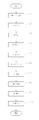
도1은 종래의 프린트기판의 제조방법에 대한 공정도이다.1 is a process chart of a conventional method for manufacturing a printed board.
도1을 참조하여 설명하면 먼저 쓰루홀용 관통구멍을 다수 드릴링 한 후, 소프트에칭을 하여 드라이필름의 밀착력을 증진시킬 수 있도록 한다. Referring to FIG. 1, first, a plurality of through holes for through holes are drilled, and then soft etching is performed to increase the adhesion of the dry film.
그 다음 무전해동도금을 실시한 후, 드라이필름을 코팅하고, 코팅 위에 회로가 그려진 필름을 올려놓고 노광 및 현상을 한다.Then, after electroless copper plating, the dry film is coated, and a film on which the circuit is drawn is placed on the coating, followed by exposure and development.
다음으로 유산동도금을 실시한 후, 금속 표면에 코팅된 코팅층을 제거하는 박리단계를 거치면 소프트에칭을 하여 회로기판의 제작이 완료된다. Next, after performing lactic acid copper plating, a peeling step of removing the coating layer coated on the metal surface is performed to soft etch to complete the manufacture of the circuit board.
본 발명은 상기와 같은 문제점을 해결할 수 있도록 제안된 것으로, The present invention is proposed to solve the above problems,
본 발명의 목적은 홀의 구리도금 두께를 균일하게 하는 것과 이후 패턴형성을 위한 DFR(DRY FILM RESISTER)의 코팅을 쉽게 할 수 있는 장점이 있어서 버튼 형성 이후 패턴공정에서 FINE PATTERN을 형성할 수 있으며, An object of the present invention is to uniformize the thickness of the copper plating of the hole and to facilitate the coating of DFR (DRY FILM RESISTER) for pattern formation afterwards to form a fine pattern in the pattern process after button formation,
양면 FPCB의 원재료인 FCCL이 롤(ROLL)또는 시트(SHEET) 상태로 진행이 가능함으로 기존 버튼공법에서 굴곡특성 및 신뢰성의 측면에서 월등한 효과를 도출할 수 있어 양호한 품질을 가진 PCB를 생산할 수 있도록 하는 프린트기판의 제조방법을 제공하는 것을 그 목적으로 한다.FCCL, a raw material of double-sided FPCB, can be rolled or sheeted to produce superior quality PCBs with excellent effects in terms of bending characteristics and reliability. It is an object of the present invention to provide a method for manufacturing a printed circuit board.
본 발명은 상기와 같은 목적을 달성하기 위하여 하기와 같은 실시예를 포함한다. The present invention includes the following embodiments in order to achieve the above object.
본 발명의 일 실시예에 따르면, 드릴링으로 기판의 표면에 홀(HOLE)을 형성하는 단계와,According to one embodiment of the invention, the step of forming a hole (HOLE) on the surface of the substrate by drilling,
드릴링된 기판에 화학동을 실시하는 단계;Performing chemical copper on the drilled substrate;
화학동이 입혀진 기판에 전기동도금을 실시하는 단계;Performing electroplating on the substrate coated with chemical copper;
전기동도금이 입혀진 기판에 밀착력을 증진시키기 위한 전처리과정인 소프트에칭을 실시하는 단계,Performing soft etching, a pretreatment process for enhancing adhesion to the electroplated substrate,
소프트에칭이 실시된 기판에 드라이필름을 코팅 및 노광을 실시하는 단계,Coating and exposing the dry film to the substrate subjected to soft etching,
노광된 기판에 현상을 실시하는 단계,Developing on the exposed substrate,
현상된 기판에 하프에칭을 하는 단계,Half etching the developed substrate,
하프에칭된 상기 기판에 드라이필름을 박리하는 단계,Peeling a dry film on the half-etched substrate,
드라이 필름이 박리된 기판에 소프트에칭을 실시하여 회로패턴이 형성되는 단계를 포함하는 것을 특징으로 한다.
And performing a soft etching on the substrate from which the dry film is peeled off, thereby forming a circuit pattern.
본 발명의 다른 실시예에 따르면, 상기 기판은 유연한 플랙시블 프린트 기판을 사용하는 것을 특징으로 한다.
According to another embodiment of the present invention, the substrate is characterized by using a flexible flexible printed substrate.
본 발명의 또 다른 실시예에 따르면, 상기 전기동도금 처리까지 공정된 기판은 부착될 드라이 필름의 밀착력을 증진시키기 위한 전처리과정인 SOFT에칭을 실시하고 HALF에칭을 하여 홀이 아닌 기판의 바깥표면에 형성된 동도금을 제거할 수 있도록 하는 것을 특징으로 한다.
According to another embodiment of the present invention, the substrate processed up to the electroplating process is subjected to SOFT etching, which is a pretreatment process to enhance the adhesion of the dry film to be attached, and is formed on the outer surface of the substrate rather than the hole by HALF etching It is characterized in that the copper plating can be removed.
본 발명의 또 다른 실시예에 따르면, 상기 드라이필름의 노광단계에서는 쓰루홀을 노출시켜 경화하여 홀이 아닌 부위가 현상공정에서 현상되어서 동이 노출되게 노광공정을 진행하는 것을 특징으로 한다.
According to another embodiment of the present invention, in the exposing step of the dry film, the through-holes are exposed and cured so that a portion other than the holes is developed in the developing process, so that the copper is exposed.
본 발명의 또 다른 실시예에 따르면, 상기 하프에칭단계는 회로의 패턴이 아닌 노출된 동박을 도금이 형성된 두께까지 제거하여 얇게 형성함으로서 패턴이 FINE화 됨에 따라 동의 두께를 얇게 하여 패턴재현을 원활히 할 수 있도록 하는 것을 특징으로 한다.According to another embodiment of the present invention, the half-etching step removes the exposed copper foil, not the pattern of the circuit, to a thickness in which the plating is formed to form a thin layer so that the thickness of the copper can be smoothed as the pattern is finened to smooth the pattern reproduction. It can be characterized by.
본 발명은 앞서 본 구성에 의해 다음과 같은 효과를 도모할 수 있다.
The present invention can achieve the following effects by the above configuration.
본 발명에 따른 프린트기판의 제조방법에 있어서, 홀의 안정성과 DFR(DRY FILM RESISTER)의 코팅을 쉽게 할 수 있는 장점이 있어서 버튼 형성 이후 패턴공정에서 FINE PATTERN을 형성할 수 있는 효과를 지니며,In the method of manufacturing a printed circuit board according to the present invention, the stability of the hole and the coating of DFR (DRY FILM RESISTER) can be easily coated, which has the effect of forming a fine pattern in the pattern process after button formation.
동도금의 두께 편차가 적고 모델별 도금 두께의 유의차가 없어 초기 개발품의 조건 설정이 용이한 효과를 도모할 수 있다. The small thickness variation of copper plating and no significant difference in plating thickness for each model make it easy to set the conditions for early development products.
또한, HALF에칭과 소프트에칭을 실시하여 기판의 두께를 줄일 수 있을 뿐만 아니라 미세회로를 용이하게 형성하는 것이 가능하며, 층간 전기적 신뢰도가 높으므로 양면 또는 다층 인쇄회로기판의 제조에 적합한 효과가 있다.In addition, by performing HALF etching and soft etching, it is possible not only to reduce the thickness of the substrate, but also to easily form a fine circuit. Since the interlayer electrical reliability is high, there is an effect suitable for the manufacture of double-sided or multilayer printed circuit boards.
도 1은 종래의 프린트기판의 제조방법에 대한 공정도
도 2는 본 발명의 일 실시예에 따른 프린트기판의 제조방법의 순서도
도 3은 본 발명의 일 실시예에 따른 프린트기판의 제조방법의 공정도1 is a process chart for a manufacturing method of a conventional printed board
2 is a flow chart of a method of manufacturing a printed board according to an embodiment of the present invention.
Figure 3 is a process diagram of a manufacturing method of a printed circuit board according to an embodiment of the present invention.
이하, 본 발명의 바람직한 실시예를 첨부된 도면들을 참조하여 상세히 설명한다. 우선 각 도면의 구성요소들에 참조부호를 부가함에 있어서, 동일한 구성요소들에 대해서는 비록 다른 도면상에 표시되더라도 가능한 한 동일한 부호를 가지도록 하고 있음에 유의해야 한다. 또한, 본 발명을 설명함에 있어서, 관련된 공지 구성 또는 기능에 대한 구체적인 설명이 본 발명이 요지를 흐릴 수 있다고 판단되는 경우에는 그 상세한 설명은 생략한다.
Hereinafter, exemplary embodiments of the present invention will be described in detail with reference to the accompanying drawings. First of all, in adding reference numerals to the components of each drawing, it should be noted that the same reference numerals are used as much as possible even if displayed on different drawings. In addition, in describing the present invention, if it is determined that the detailed description of the related well-known configuration or function may obscure the subject matter, the detailed description thereof will be omitted.
도 2는 본 발명의 일 실시예에 따른 프린트기판의 제조방법의 순서도이고, 도 3은 본 발명의 일 실시예에 따른 프린트기판의 제조방법의 공정도이다.
2 is a flowchart of a method of manufacturing a printed board according to an embodiment of the present invention, and FIG. 3 is a process diagram of a method of manufacturing a printed board according to an embodiment of the present invention.
도 2를 참조하여 설명하면, 본 발명인 프린트기판의 제조방법은 우선 드릴링으로 플랙시블 회로기판(Flexible Printed Circuit Board: F.P.C.B)의 표면에 홀(HOLE)을 형성한다(S10). 드릴링된 기판에 소프트에칭(S20)을 실시한 후, 화학동을 실시한다(320).Referring to FIG. 2, the method of manufacturing a printed circuit board according to the present invention first forms a hole (HOLE) on the surface of a flexible printed circuit board (F.P.C.B) by drilling (S10). After performing soft etching (S20) on the drilled substrate, chemical copper is performed (320).
화학동을 형성한 후 전기동도금을 실시한다(S40). 다음으로 밀착력을 증진시키기 위한 전처리과정인 SOFT에칭을 실시한다(S50). 그리고 배경기술에서 예시한 드라이필름의 코팅 및 노광을 실시한다(S60). 노광된 기판에 현상을 실시한다(S70).After forming the copper copper is subjected to electroplating (S40). Next, SOFT etching is performed, which is a pretreatment process to enhance adhesion (S50). And the coating and exposure of the dry film exemplified in the background art (S60). Development is performed on the exposed substrate (S70).
다음 단계로 HALF에칭을 한다(S80). Next, HALF etching is performed (S80).
상기 HALF에칭 후에는 드리이필름의 박리(S90)과정을 거쳐 다시 한번 SOFT에칭을 실시하여 회로패턴이 형성된다(S100).
After the HALF etching, the circuit pattern is formed by performing SOFT etching once again through the process of peeling the dry film (S90) (S100).
먼저 프린트 기판(E)는 유연한 플랙시블 프린트 기판(FPC)과, 경질의 리지드 프린트 기판으로 크게 구별되지만, 본원 발명에서는 플랙시블 프린트 기판(FPC)을 사용하며, 상기 플랙시블 프린트 기판(FPC)은 절연재(플렉서블 기판의 경우는 절연 필름(insulating film)이라고도 한다)의 양면에 각각 구리박이 붙여진, 양면에 구리를 붙인 적층판으로 된다. 베이스재인 절연재는 플렉시블 프린트 기판의 경우는 폴리이미드 수지제 필름(polyimide resin film), 아라미드 수지제 필름(aramid resin film), 액정 폴리머제 필름(liquid crystal polymer film), 그 밖의 유연성과 절연성을 구비한 수지제 필름으로 된다. 구리박로서는, 압연박(rolled foil), 전해박(electrolytic foil), 특수 전해박, 또는 도금박(plating foil) 등이 사용된다.First, the printed board E is largely divided into a flexible flexible printed board (FPC) and a rigid rigid printed board, but in the present invention, a flexible printed board (FPC) is used, and the flexible printed board (FPC) is It becomes a laminated board which affixed copper on both surfaces by which copper foil was affixed on both surfaces of an insulating material (also called an insulating film in the case of a flexible substrate). Insulating material, which is a base material, has a polyimide resin film, an aramid resin film, a liquid crystal polymer film, and other flexibility and insulation for flexible printed circuit boards. It becomes a resin film. As the copper foil, a rolled foil, an electrolytic foil, a special electrolytic foil, a plating foil, or the like is used.
또한, 이러한 절연재로서는, 복층 타입(double layer type)의 것과 단층 타입(single layer type)의 것이 있다. 복층 타입에서는, 절연재의 양면에, 접착제를 매개로 하여 각각 구리박이 적층된다. 접착제로서는 에폭시(epoxy) 수지, 할로겐 프리(halogen free) 에폭시 수지, 또는 고(高) Tg-에폭시 수지 등이 사용된다. 이에 대해서 단층 타입에서는, 절연재의 양면에 각각 구리박(F)가 직접 첩부 적층된다. 단층 타입의 절연재는 캐스팅법(casting method), 라미네이터법(laminator method), 또는 메탈라이딩법(metalliding method), 스퍼터링법(sputtering method) 등에 의해 제작된다.
As such an insulating material, there are a double layer type and a single layer type. In the multilayer type, copper foil is laminated on both surfaces of an insulating material via an adhesive agent, respectively. As the adhesive, an epoxy resin, a halogen free epoxy resin, a high Tg-epoxy resin, or the like is used. In contrast, in the single layer type, the copper foils F are directly laminated on both surfaces of the insulating material. The single layer type insulating material is produced by a casting method, a laminator method, a metalliding method, a sputtering method, or the like.
상기 플랙시블 프린트 기판(FPC)을 이용한 제조방법을 살펴보면, 도3에 도시된 바와 같이, 기판에 쓰루홀(1)용의 관통구멍(2)가 다수 드릴링 가공된다.Looking at the manufacturing method using the flexible printed circuit board (FPC), as shown in Figure 3, a plurality of through holes for the through-hole (1) in the substrate is drilled.
쓰루홀(1)은 프린트 기판(E)의 양면(표면과 이면)(한쪽 면과 반대 면) 사이를 관통하는 미세구멍(minute pore)으로 되고, 1장의 프린트 기판(E)에 다수 형성된다. 그리고 쓰루홀(1)은, 양면의 회로 패턴(A) 사이의 도통 접속용, 또는(및) 회로 패턴(A)에 실장(mounting)되는 반도체부품 등의 부착용으로서 사용된다. 쓰루홀(1)의 공경(孔徑)은 0.2 ㎜ 이상~0.5 ㎜ 이하의 것이 많아지고 있고, 드릴공법에 의한 것으로 0.1 ㎜ 정도인 것, 레이저공법의 것으로는 0.05 ㎜ 정도인 것도 출현하고 있다.Through-
쓰루홀(1)이 가공된 기판(E)에 화학동 처리를 하여 도전성 피막(2)이 형성된다. 상기 화학동 처리는 무전해 동도금 공정을 말하며, 화학 또는 촉매도금이라고도 한다. 상기 쓰루홀의 내벽에 전도체인 동을 입혀 전도성을 부여하며, 도금되는 동의 두께는 0.3~1.0㎛이고, 사용되는 촉매는 Pd가 주로 사용된다.
The electrochemical copper process is performed to the board | substrate E with which the through-
상기 화학동 처리된 기판에는 다시 전기동도금이 처리하여 상기 도전성 피막(2)의 상부에 동도금(3)이 형성된다. 전기 동도금은 패턴 및 홀의 내벽에 규정된 두께의 동을 전기석출법을 사용하여 2차 도금하는 공정으로 석출량은 전류밀도와 석출시간으로 결정된다.
Electrochemical copper plating is again performed on the chemically copper-treated substrate to form copper plating 3 on the
상기 전기동도금처리까지 공정된 기판은 추후 부착될 드라이 필름의 밀착력을 증진시키기 위한 전처리과정인 SOFT에칭을 실시하여 기판(E)의 바깥표면에 형성된 상기 동도금(3)을 제거한다.
The substrate processed until the electrocopper plating process is subjected to SOFT etching, which is a pretreatment process for enhancing the adhesion of the dry film to be attached later, to remove the copper plating 3 formed on the outer surface of the substrate E.
그 다음, 제조방법에서는 정면처리된 기판(E)상에 드라이필름(4)을 정해진 열과 압력을 압착하여 도포한 뒤, 상기 드라이필름(4)의 위에 워킹필름을 정합하여 노광시간동안 빛에너지를 공급하여 필요한 패턴 이미지를 재현해 낼 수 있도록 한다. 한편 본원발명에서는 상기 쓰루홀(1)을 가린 상태에서 노광공정을 진행하는 것이 바람직하다.Next, in the manufacturing method, the
그리고, 드라이 필름(4)등으로 피복된 기판(E)이 현상되는데, 기판(E)의 쓰루홀(1)을 통해 현상액을 침입시켜 상기 드라이필름(4)을 현상액으로 용해시켜 제거될 수 있도록 한다.
Then, the substrate E coated with the
현상과정을 거친 기판(E)은 HALF에칭 단계를 거치게 되는데, 여기서 HALF에칭은 기존에 없는 공정으로 Pattern이 FINE화 됨에 따라 동의 두께를 얇게 하여 Pattern재현을 원활히 하려는 목적으로 사용하며, 보통 1/2 OZ나 1/4 OZ의 동박을 균일하게 에칭하여 원하는 두께로 만드는 공정이나 본 발명에서는 홀이 아닌 노출된 동박표면을 도금이 형성된 두께까지 제거하여 얇게 형성한다.
The developed substrate (E) goes through the HALF etching step, where HALF etching is a process that does not exist in the past, and is used for the purpose of smoothing the pattern reproduction by thinning the copper thickness as the pattern is finened. In the process of uniformly etching OZ or 1/4 OZ copper foil to a desired thickness or in the present invention, the exposed copper foil surface, not the hole, is removed to the thickness where the plating is formed to form a thin layer.
그 다음, 드라이 필름(4)을 박리하여 제거한 후, 소프트에칭을 실시하여 인쇄회로기판의 두께를 좀 더 얇게 할 수 있고, 동적층판의 표면에 미세회로를 형성하는 것이 용이하도록 할 수 있다.
Then, after peeling and removing the
이상의 설명은 본 발명의 기술 사상을 예시적으로 설명한 것에 불과한 것으로서, 본 발명이 속하는 기술 분야에서 통상의 지식을 가진 자라면 본 발명의 본질적인 특성에서 벗어나지 않는 범위에서 다양한 수정 및 변형이 가능할 것이다. 따라서, 본 발명에 개시된 실시예들은 본 발명의 기술 사상을 한정하기 위한 것이 아니라 설명하기 위한 것이고, 이러한 실시예에 의하여 본 발명의 기술 사상의 범위가 한정되는 것은 아니다. 본 발명의 보호범위는 아래 청구범위에 의하여 해석되어야 하며, 그와 동등한 범위 내에 있는 모든 기술 사상은 본 발명의 권리범위에 포함되는 것으로 해석되어야 할 것이다.The foregoing description is merely illustrative of the technical idea of the present invention, and various changes and modifications may be made by those skilled in the art without departing from the essential characteristics of the present invention. Therefore, the embodiments disclosed in the present invention are not intended to limit the technical idea of the present invention but to describe the present invention, and the scope of the technical idea of the present invention is not limited by these embodiments. The scope of protection of the present invention should be interpreted by the following claims, and all technical ideas within the scope equivalent thereto should be construed as being included in the scope of the present invention.
E : 기판 1 : 쓰루홀
2 : 도전성 피막 3 : 동도금
4 : 드라이 필름E: Substrate 1: Through Hole
2: conductive film 3: copper plating
4: dry film
Claims (5)
드릴링된 기판에 소프트에칭을 실시하는 단계,
소프트에칭이 실시된 기판에 화학동을 실시하는 단계;
화학동이 입혀진 기판에 전기동도금을 실시하는 단계,
전기동도금이 입혀진 기판에 밀착력을 증진시키기 위한 전처리과정인 소프트에칭을 실시하는 단계,
소프트에칭이 실시된 기판에 드라이필름을 코팅 및 노광을 실시하는 단계,
노광된 기판에 현상을 실시하는 단계,
현상된 기판에 하프에칭을 하는 단계,
하프에칭된 상기 기판에 드라이필름의 박리하는 단계,
드라이 필름이 박리된 기판에 소프트에칭을 실시하여 회로패턴이 형성되는 단계를 포함하는 것을 특징으로 하는 프린트기판의 제조방법Drilling to form a hole (HOLE) in the surface of the substrate,
Performing soft etching on the drilled substrate,
Performing chemical copper on the substrate subjected to soft etching;
Electroplating the chemically coated substrate,
Performing soft etching, a pretreatment process for enhancing adhesion to the electroplated substrate,
Coating and exposing the dry film to the substrate subjected to soft etching,
Developing on the exposed substrate,
Half etching the developed substrate,
Peeling the dry film onto the half-etched substrate,
Method of manufacturing a printed circuit board comprising the step of performing a soft etching on the substrate from which the dry film is peeled off to form a circuit pattern
상기 기판은 유연한 플랙시블 프린트 기판을 사용하는 것을 특징으로 하는 프린트기판의 제조방법The method of claim 1,
The substrate is a manufacturing method of a printed circuit board, characterized in that using a flexible flexible printed circuit board
상기 전기동도금 처리까지 공정된 기판은 부착될 드라이 필름의 밀착력을 증진시키기 위한 전처리과정인 SOFT에칭을 실시하고 HALF에칭을 하여 홀이 아닌 기판의 바깥표면에 형성된 동도금을 제거할 수 있도록 하는 것을 특징으로 하는 프린트기판의 제조방법The method of claim 1,
The substrate processed to the electroplating process is subjected to SOFT etching, which is a pretreatment process to enhance the adhesion of the dry film to be attached, and by HALF etching to remove the copper plating formed on the outer surface of the substrate, not the hole Manufacturing method of printed circuit board
상기 드라이필름의 노광단계에서는 쓰루홀을 노출시켜 경화하여 홀이 아닌 부위가 현상공정에서 현상되어서 동이 노출되게 노광공정을 진행하는 것을 특징으로 하는 프린트기판의 제조방법The method of claim 1,
In the exposure step of the dry film, the through-holes are exposed and cured so that the non-holes are developed in the developing step, and the exposure process is performed so that the copper is exposed.
상기 하프에칭단계는 회로의 패턴이 아닌 노출된 동박을 도금이 형성된 두께까지 제거하여 얇게 형성함으로서 패턴이 FINE화 됨에 따라 동의 두께를 얇게 하여 패턴재현을 원활히 할 수 있도록 하는 것을 특징으로 하는 프린트기판의 제조방법The method of claim 1,
The half-etching step is to remove the exposed copper foil, not the pattern of the circuit, to a thickness formed by plating to form a thin, thereby reducing the thickness of the copper as the pattern is finened to facilitate the pattern reproduction of the printed circuit board Manufacturing method
Priority Applications (1)
| Application Number | Priority Date | Filing Date | Title |
|---|---|---|---|
| KR1020100068702A KR20120007909A (en) | 2010-07-15 | 2010-07-15 | Manufacturing Method of Printed Board |
Applications Claiming Priority (1)
| Application Number | Priority Date | Filing Date | Title |
|---|---|---|---|
| KR1020100068702A KR20120007909A (en) | 2010-07-15 | 2010-07-15 | Manufacturing Method of Printed Board |
Publications (1)
| Publication Number | Publication Date |
|---|---|
| KR20120007909A true KR20120007909A (en) | 2012-01-25 |
Family
ID=45613097
Family Applications (1)
| Application Number | Title | Priority Date | Filing Date |
|---|---|---|---|
| KR1020100068702A Ceased KR20120007909A (en) | 2010-07-15 | 2010-07-15 | Manufacturing Method of Printed Board |
Country Status (1)
| Country | Link |
|---|---|
| KR (1) | KR20120007909A (en) |
Cited By (8)
| Publication number | Priority date | Publication date | Assignee | Title |
|---|---|---|---|---|
| CN102883542A (en) * | 2012-10-17 | 2013-01-16 | 无锡江南计算技术研究所 | Production method of substrate surface circuit diagraph |
| KR101223400B1 (en) * | 2012-08-07 | 2013-01-16 | 주식회사 와이에스테크 | Side plating method of substrate outskirts |
| CN103582306A (en) * | 2012-08-06 | 2014-02-12 | Si弗莱克斯有限公司 | Printed circuit board manufacturing method |
| KR101380016B1 (en) * | 2012-07-25 | 2014-04-02 | 강병돈 | The manufacturing method of bandpass filters of microstrip line |
| KR101420924B1 (en) * | 2012-09-17 | 2014-07-25 | 풍원정밀(주) | Method for manufacturing of thin metal substrate and thin metal substrate using the same method |
| CN105208778A (en) * | 2015-09-23 | 2015-12-30 | 安捷利电子科技(苏州)有限公司 | Manufacturing mode for producing high-density flexible printed circuit board in sheet mode |
| CN111867240A (en) * | 2020-05-25 | 2020-10-30 | 鹤山市中富兴业电路有限公司 | High-pressure-resistant material and method for improving pressure resistance of PCB |
| CN119730071A (en) * | 2024-12-24 | 2025-03-28 | 厦门弘信电子科技集团股份有限公司 | Manufacturing method of wireless FPC (Flexible printed Circuit) |
-
2010
- 2010-07-15 KR KR1020100068702A patent/KR20120007909A/en not_active Ceased
Cited By (9)
| Publication number | Priority date | Publication date | Assignee | Title |
|---|---|---|---|---|
| KR101380016B1 (en) * | 2012-07-25 | 2014-04-02 | 강병돈 | The manufacturing method of bandpass filters of microstrip line |
| CN103582306A (en) * | 2012-08-06 | 2014-02-12 | Si弗莱克斯有限公司 | Printed circuit board manufacturing method |
| KR101223400B1 (en) * | 2012-08-07 | 2013-01-16 | 주식회사 와이에스테크 | Side plating method of substrate outskirts |
| KR101420924B1 (en) * | 2012-09-17 | 2014-07-25 | 풍원정밀(주) | Method for manufacturing of thin metal substrate and thin metal substrate using the same method |
| CN102883542A (en) * | 2012-10-17 | 2013-01-16 | 无锡江南计算技术研究所 | Production method of substrate surface circuit diagraph |
| CN105208778A (en) * | 2015-09-23 | 2015-12-30 | 安捷利电子科技(苏州)有限公司 | Manufacturing mode for producing high-density flexible printed circuit board in sheet mode |
| CN111867240A (en) * | 2020-05-25 | 2020-10-30 | 鹤山市中富兴业电路有限公司 | High-pressure-resistant material and method for improving pressure resistance of PCB |
| CN119730071A (en) * | 2024-12-24 | 2025-03-28 | 厦门弘信电子科技集团股份有限公司 | Manufacturing method of wireless FPC (Flexible printed Circuit) |
| CN119730071B (en) * | 2024-12-24 | 2025-11-18 | 厦门弘信电子科技集团股份有限公司 | A method for manufacturing a wireless charging FPC |
Similar Documents
| Publication | Publication Date | Title |
|---|---|---|
| KR20120007909A (en) | Manufacturing Method of Printed Board | |
| CN108617104B (en) | Method for manufacturing printed circuit board with thickened copper local pattern | |
| KR100733253B1 (en) | High density printed circuit board and manufacturing method thereof | |
| JP6819608B2 (en) | Multi-layer printed wiring board and its manufacturing method | |
| KR100661713B1 (en) | Printed wiring board manufacturing method | |
| US11140784B2 (en) | Printed wiring board and manufacturing method thereof | |
| CN102378483A (en) | Printed circuit board and method of manufacturing the same | |
| KR20040075595A (en) | Method for manufacturing double side a flexible printed circuit board | |
| KR100700272B1 (en) | Manufacturing Method of Printed Board | |
| JPH04100294A (en) | Manufacture of printed wiring board | |
| KR101201948B1 (en) | The printed circuit board manufacturing method | |
| KR20090011528A (en) | Manufacturing method of printed circuit board | |
| KR20110009790A (en) | Flexible Printed Circuit Board and Manufacturing Method Thereof | |
| JP4549807B2 (en) | Multilayer printed wiring board manufacturing method, multilayer printed wiring board, and electronic device | |
| KR101241070B1 (en) | The printed circuit board manufacturing method | |
| CN114641136B (en) | Manufacturing method of copper layer boss of circuit board and circuit board | |
| JPH10215072A (en) | Manufacture of multilayer printed wiring board | |
| JP2004039771A (en) | Manufacturing method of printed circuit board | |
| JP2012074557A (en) | Multilayer printed wiring board and manufacturing method therefor, and multilayer build-up wiring board and manufacturing method therefor | |
| JPH036880A (en) | Blind wiring board and its manufacturing method | |
| KR101041130B1 (en) | Printed Circuit Board Manufacturing Method Using Nickel Plating | |
| CN120076205B (en) | A method for manufacturing high-precision circuit boards with single-sided through-hole rings | |
| JPH077264A (en) | Manufacture of printed wiring board | |
| JPH08204339A (en) | Manufacture of printed wiring board | |
| JP2000138443A (en) | Manufacture of conductor pattern |
Legal Events
| Date | Code | Title | Description |
|---|---|---|---|
| A201 | Request for examination | ||
| PA0109 | Patent application |
Patent event code: PA01091R01D Comment text: Patent Application Patent event date: 20100715 |
|
| PA0201 | Request for examination | ||
| E902 | Notification of reason for refusal | ||
| PE0902 | Notice of grounds for rejection |
Comment text: Notification of reason for refusal Patent event date: 20110714 Patent event code: PE09021S01D |
|
| E601 | Decision to refuse application | ||
| PE0601 | Decision on rejection of patent |
Patent event date: 20111223 Comment text: Decision to Refuse Application Patent event code: PE06012S01D Patent event date: 20110714 Comment text: Notification of reason for refusal Patent event code: PE06011S01I |
|
| PG1501 | Laying open of application |