KR20100135223A - Light emitting diode package - Google Patents
Light emitting diode package Download PDFInfo
- Publication number
- KR20100135223A KR20100135223A KR1020107017068A KR20107017068A KR20100135223A KR 20100135223 A KR20100135223 A KR 20100135223A KR 1020107017068 A KR1020107017068 A KR 1020107017068A KR 20107017068 A KR20107017068 A KR 20107017068A KR 20100135223 A KR20100135223 A KR 20100135223A
- Authority
- KR
- South Korea
- Prior art keywords
- light emitting
- emitting diode
- glass
- substrate
- conductor
- Prior art date
- Legal status (The legal status is an assumption and is not a legal conclusion. Google has not performed a legal analysis and makes no representation as to the accuracy of the status listed.)
- Ceased
Links
Images
Classifications
-
- C—CHEMISTRY; METALLURGY
- C04—CEMENTS; CONCRETE; ARTIFICIAL STONE; CERAMICS; REFRACTORIES
- C04B—LIME, MAGNESIA; SLAG; CEMENTS; COMPOSITIONS THEREOF, e.g. MORTARS, CONCRETE OR LIKE BUILDING MATERIALS; ARTIFICIAL STONE; CERAMICS; REFRACTORIES; TREATMENT OF NATURAL STONE
- C04B35/00—Shaped ceramic products characterised by their composition; Ceramics compositions; Processing powders of inorganic compounds preparatory to the manufacturing of ceramic products
- C04B35/01—Shaped ceramic products characterised by their composition; Ceramics compositions; Processing powders of inorganic compounds preparatory to the manufacturing of ceramic products based on oxide ceramics
- C04B35/10—Shaped ceramic products characterised by their composition; Ceramics compositions; Processing powders of inorganic compounds preparatory to the manufacturing of ceramic products based on oxide ceramics based on aluminium oxide
- C04B35/111—Fine ceramics
- C04B35/117—Composites
- C04B35/119—Composites with zirconium oxide
-
- C—CHEMISTRY; METALLURGY
- C03—GLASS; MINERAL OR SLAG WOOL
- C03C—CHEMICAL COMPOSITION OF GLASSES, GLAZES OR VITREOUS ENAMELS; SURFACE TREATMENT OF GLASS; SURFACE TREATMENT OF FIBRES OR FILAMENTS MADE FROM GLASS, MINERALS OR SLAGS; JOINING GLASS TO GLASS OR OTHER MATERIALS
- C03C14/00—Glass compositions containing a non-glass component, e.g. compositions containing fibres, filaments, whiskers, platelets, or the like, dispersed in a glass matrix
- C03C14/004—Glass compositions containing a non-glass component, e.g. compositions containing fibres, filaments, whiskers, platelets, or the like, dispersed in a glass matrix the non-glass component being in the form of particles or flakes
-
- C—CHEMISTRY; METALLURGY
- C04—CEMENTS; CONCRETE; ARTIFICIAL STONE; CERAMICS; REFRACTORIES
- C04B—LIME, MAGNESIA; SLAG; CEMENTS; COMPOSITIONS THEREOF, e.g. MORTARS, CONCRETE OR LIKE BUILDING MATERIALS; ARTIFICIAL STONE; CERAMICS; REFRACTORIES; TREATMENT OF NATURAL STONE
- C04B35/00—Shaped ceramic products characterised by their composition; Ceramics compositions; Processing powders of inorganic compounds preparatory to the manufacturing of ceramic products
- C04B35/01—Shaped ceramic products characterised by their composition; Ceramics compositions; Processing powders of inorganic compounds preparatory to the manufacturing of ceramic products based on oxide ceramics
- C04B35/10—Shaped ceramic products characterised by their composition; Ceramics compositions; Processing powders of inorganic compounds preparatory to the manufacturing of ceramic products based on oxide ceramics based on aluminium oxide
- C04B35/111—Fine ceramics
- C04B35/117—Composites
-
- H—ELECTRICITY
- H10—SEMICONDUCTOR DEVICES; ELECTRIC SOLID-STATE DEVICES NOT OTHERWISE PROVIDED FOR
- H10H—INORGANIC LIGHT-EMITTING SEMICONDUCTOR DEVICES HAVING POTENTIAL BARRIERS
- H10H20/00—Individual inorganic light-emitting semiconductor devices having potential barriers, e.g. light-emitting diodes [LED]
- H10H20/80—Constructional details
- H10H20/85—Packages
- H10H20/8506—Containers
-
- H—ELECTRICITY
- H10—SEMICONDUCTOR DEVICES; ELECTRIC SOLID-STATE DEVICES NOT OTHERWISE PROVIDED FOR
- H10H—INORGANIC LIGHT-EMITTING SEMICONDUCTOR DEVICES HAVING POTENTIAL BARRIERS
- H10H20/00—Individual inorganic light-emitting semiconductor devices having potential barriers, e.g. light-emitting diodes [LED]
- H10H20/80—Constructional details
- H10H20/85—Packages
- H10H20/858—Means for heat extraction or cooling
- H10H20/8581—Means for heat extraction or cooling characterised by their material
-
- H—ELECTRICITY
- H10—SEMICONDUCTOR DEVICES; ELECTRIC SOLID-STATE DEVICES NOT OTHERWISE PROVIDED FOR
- H10W—GENERIC PACKAGES, INTERCONNECTIONS, CONNECTORS OR OTHER CONSTRUCTIONAL DETAILS OF DEVICES COVERED BY CLASS H10
- H10W40/00—Arrangements for thermal protection or thermal control
- H10W40/20—Arrangements for cooling
- H10W40/22—Arrangements for cooling characterised by their shape, e.g. having conical or cylindrical projections
- H10W40/226—Arrangements for cooling characterised by their shape, e.g. having conical or cylindrical projections characterised by projecting parts, e.g. fins to increase surface area
- H10W40/228—Arrangements for cooling characterised by their shape, e.g. having conical or cylindrical projections characterised by projecting parts, e.g. fins to increase surface area the projecting parts being wire-shaped or pin-shaped
-
- C—CHEMISTRY; METALLURGY
- C04—CEMENTS; CONCRETE; ARTIFICIAL STONE; CERAMICS; REFRACTORIES
- C04B—LIME, MAGNESIA; SLAG; CEMENTS; COMPOSITIONS THEREOF, e.g. MORTARS, CONCRETE OR LIKE BUILDING MATERIALS; ARTIFICIAL STONE; CERAMICS; REFRACTORIES; TREATMENT OF NATURAL STONE
- C04B2235/00—Aspects relating to ceramic starting mixtures or sintered ceramic products
- C04B2235/02—Composition of constituents of the starting material or of secondary phases of the final product
- C04B2235/30—Constituents and secondary phases not being of a fibrous nature
- C04B2235/36—Glass starting materials for making ceramics, e.g. silica glass
-
- C—CHEMISTRY; METALLURGY
- C04—CEMENTS; CONCRETE; ARTIFICIAL STONE; CERAMICS; REFRACTORIES
- C04B—LIME, MAGNESIA; SLAG; CEMENTS; COMPOSITIONS THEREOF, e.g. MORTARS, CONCRETE OR LIKE BUILDING MATERIALS; ARTIFICIAL STONE; CERAMICS; REFRACTORIES; TREATMENT OF NATURAL STONE
- C04B2235/00—Aspects relating to ceramic starting mixtures or sintered ceramic products
- C04B2235/60—Aspects relating to the preparation, properties or mechanical treatment of green bodies or pre-forms
- C04B2235/602—Making the green bodies or pre-forms by moulding
- C04B2235/6025—Tape casting, e.g. with a doctor blade
-
- C—CHEMISTRY; METALLURGY
- C04—CEMENTS; CONCRETE; ARTIFICIAL STONE; CERAMICS; REFRACTORIES
- C04B—LIME, MAGNESIA; SLAG; CEMENTS; COMPOSITIONS THEREOF, e.g. MORTARS, CONCRETE OR LIKE BUILDING MATERIALS; ARTIFICIAL STONE; CERAMICS; REFRACTORIES; TREATMENT OF NATURAL STONE
- C04B2235/00—Aspects relating to ceramic starting mixtures or sintered ceramic products
- C04B2235/70—Aspects relating to sintered or melt-casted ceramic products
- C04B2235/96—Properties of ceramic products, e.g. mechanical properties such as strength, toughness, wear resistance
-
- H—ELECTRICITY
- H05—ELECTRIC TECHNIQUES NOT OTHERWISE PROVIDED FOR
- H05K—PRINTED CIRCUITS; CASINGS OR CONSTRUCTIONAL DETAILS OF ELECTRIC APPARATUS; MANUFACTURE OF ASSEMBLAGES OF ELECTRICAL COMPONENTS
- H05K1/00—Printed circuits
- H05K1/02—Details
- H05K1/0201—Thermal arrangements, e.g. for cooling, heating or preventing overheating
- H05K1/0203—Cooling of mounted components
- H05K1/0204—Cooling of mounted components using means for thermal conduction connection in the thickness direction of the substrate
- H05K1/0206—Cooling of mounted components using means for thermal conduction connection in the thickness direction of the substrate by printed thermal vias
-
- H—ELECTRICITY
- H05—ELECTRIC TECHNIQUES NOT OTHERWISE PROVIDED FOR
- H05K—PRINTED CIRCUITS; CASINGS OR CONSTRUCTIONAL DETAILS OF ELECTRIC APPARATUS; MANUFACTURE OF ASSEMBLAGES OF ELECTRICAL COMPONENTS
- H05K1/00—Printed circuits
- H05K1/02—Details
- H05K1/03—Use of materials for the substrate
- H05K1/0306—Inorganic insulating substrates, e.g. ceramic, glass
-
- H—ELECTRICITY
- H10—SEMICONDUCTOR DEVICES; ELECTRIC SOLID-STATE DEVICES NOT OTHERWISE PROVIDED FOR
- H10H—INORGANIC LIGHT-EMITTING SEMICONDUCTOR DEVICES HAVING POTENTIAL BARRIERS
- H10H20/00—Individual inorganic light-emitting semiconductor devices having potential barriers, e.g. light-emitting diodes [LED]
- H10H20/80—Constructional details
- H10H20/85—Packages
- H10H20/858—Means for heat extraction or cooling
- H10H20/8582—Means for heat extraction or cooling characterised by their shape
Landscapes
- Chemical & Material Sciences (AREA)
- Engineering & Computer Science (AREA)
- Ceramic Engineering (AREA)
- Materials Engineering (AREA)
- Organic Chemistry (AREA)
- Composite Materials (AREA)
- Manufacturing & Machinery (AREA)
- Structural Engineering (AREA)
- Dispersion Chemistry (AREA)
- Life Sciences & Earth Sciences (AREA)
- Chemical Kinetics & Catalysis (AREA)
- General Chemical & Material Sciences (AREA)
- Geochemistry & Mineralogy (AREA)
- Glass Compositions (AREA)
- Led Device Packages (AREA)
- Compositions Of Oxide Ceramics (AREA)
Abstract
절연 기판의 항절강도를 저하시키지 않고 서멀 버아의 볼록 형상 높이를 낮춘 발광 다이오드 패키지를 제공한다. 기판 상에 발광 다이오드 소자가 실장되어 있는 발광 다이오드 패키지로서, 기판이 몰 백분율 표시로 SiO2 를 57 ~ 65 %, B2O3 을 13 ~ 18 %, CaO 를 9 ~ 23 %, Al2O3 을 3 ~ 8 %, K2O 및 Na2O 중 적어도 어느 일방을 합계로 0.5 ~ 6 % 함유하는 유리 분말과 세라믹스 필러를 함유하는 유리 세라믹스 조성물을 소성하여 얻어진 것인 발광 다이오드 패키지.Provided is a light emitting diode package having a lower convex height of a thermal burr without lowering the strength of an insulating substrate. A light emitting diode package in which a light emitting diode device is mounted on a substrate, wherein the substrate has a mole percentage display of 57 to 65% SiO 2 , 13 to 18% B 2 O 3 , 9 to 23% CaO, and Al 2 O 3 a light emitting diode package to 3 ~ 8%, K 2 O and Na 2 O in a total amount obtained by at least any one firing a glass ceramic composition containing a glass powder and a ceramics filler, which contains 0.5 to 6%.
Description
본 발명은, 발광 다이오드 디바이스, 고휘도 (HB) 광 다이오드 백라이트, 디스플레이에 관련하는 광원, 자동차 조명, 장식 조명, 표지 및 광고 조명, 및 정보 디스플레이 용도를 포함하는 조명 디바이스의 형성에 바람직한 발광 다이오드 패키지, 및 그것에 사용되는 절연 기판에 관한 것이다. 여기서 발광 다이오드 패키지란 발광 다이오드 칩을 실장하여 장착하는 절연 기판 및 리플렉터를 포함하며, 본 명세서에서는 발광 장치라고 하는 경우가 있다.The present invention relates to a light emitting diode package suitable for the formation of light emitting diode devices, high brightness (HB) photodiode backlights, light sources associated with displays, automotive lighting, decorative lighting, signs and advertising lighting, and information display applications, And an insulating substrate used therein. Here, the light emitting diode package includes an insulating substrate and a reflector for mounting and mounting a light emitting diode chip, which may be referred to as a light emitting device in the present specification.
최근, 발광 다이오드 (이하, LED 라고 하는 경우가 있다) 디바이스 등 발광 소자의 고휘도, 백색화에 수반하여, 휴대전화나 대형 액정 TV 등의 백라이트에 LED 를 사용한 발광 장치가 사용되게 되었다.In recent years, with the high brightness and whitening of light emitting elements, such as a light emitting diode (hereinafter may be called LED) device, the light emitting device which used LED for backlights, such as a mobile telephone and a large liquid crystal TV, has become used.
그러나, 발광 소자의 고휘도화에 수반하여, 발광 장치로부터 발생하는 열도 증가하고 있다. 따라서, 온도 상승에 의한 발광 소자의 휘도 저하를 없애기 위해서는, 발생한 열을 발광 소자보다 신속하게 방산하는 높은 열방산성을 갖는 발광 소자용 기판 및 LED 패키지 (이하, 간단히 패키지라고 하는 경우가 있다) 가 요구되고 있다.However, with high luminance of the light emitting element, heat generated from the light emitting device is also increasing. Therefore, in order to eliminate the fall of the brightness | luminance of a light emitting element by temperature rise, the board | substrate for light emitting elements and LED package (henceforth simply a package) which has high heat dissipation property which dissipates heat which generate | occur | produces faster than a light emitting element is called for. It is becoming.
발광 장치의 기판으로는, 종래부터 배선 기판의 절연 기판에 사용되어 온 알루미나 기판이 사용되는 경우가 많았으나, 알루미나 기판은 열전도율이 작은 약 15 ~ 20 W/m·K 라는 문제가 있었다.As a substrate of the light emitting device, alumina substrates which have conventionally been used for insulating substrates of wiring boards are often used, but alumina substrates have a problem of about 15 to 20 W / m · K having a low thermal conductivity.
또, 알루미나 기판을 대신하는 것으로서 높은 열전도율을 갖는 질화알루미늄 기판이 주목받기 시작하였다. 그러나, 질화알루미늄 기판은, 원료 비용이 높고, 열팽창 계수가 4×10⁻⁶ ~ 5×10⁻⁶/ ℃ 으로 작기 때문에, 범용품인 9×10⁻⁶/ ℃ 이상의 열팽창 계수를 갖는 프린트 기판에 실장했을 때에 큰 열팽창 계수차로 인하여 접속 신뢰성이 저하된다는 문제가 있었다. 게다가 알루미나 기판이나 질화알루미늄 기판은 난소결성이기 때문에 고온 소성이 필요하여 프로세스 비용이 높아진다는 문제가 있었다.In addition, aluminum nitride substrates having high thermal conductivity have attracted attention as a substitute for alumina substrates. However, since the aluminum nitride substrate has a high raw material cost and a small coefficient of thermal expansion of 4 × 10 −6 to 5 × 10 −6 / ° C., the aluminum nitride substrate is mounted on a printed board having a thermal expansion coefficient of 9 × 10 −6 / ° C. or more, which is a general-purpose product. There was a problem that connection reliability was lowered due to a large thermal expansion coefficient difference. In addition, since alumina substrates and aluminum nitride substrates are poorly sintered, there is a problem that high temperature firing is required and the process cost is high.
이와 같은 문제를 해결하기 위해서, LED 패키지 기판으로서 저온 동시 소성 세라믹 기판 (이하, LTCC 또는 LTCC 기판으로 기재하는 경우가 있다) 이 사용되게 되었다.In order to solve such a problem, a low temperature co-fired ceramic substrate (hereinafter sometimes referred to as LTCC or LTCC substrate) has been used as the LED package substrate.
LTCC 는, 유리와 알루미나 필러 등 세라믹스 필러로 이루어지고, 그 유리의 굴절률과 세라믹스 필러의 굴절률차가 크고, 또한, LTCC 중에 분산되어 있는 세라믹스 필러의 수가 많기 때문에 광을 반사하는 계면의 면적이 크고, 게다가 그 계면 양측의 유리 또는 세라믹스 필러의 두께가 광의 파장보다 크기 때문에 반사율이 높다. 따라서, LTCC 는 발광 소자로부터의 광을 효율적으로 반사할 수 있고, 또 그 결과로 열 발생을 줄일 수 있다.LTCC consists of ceramic fillers such as glass and alumina fillers, and the refractive index difference between the glass and the ceramic filler is large, and the number of ceramic fillers dispersed in the LTCC is large, so that the area of the interface reflecting light is large. Since the thickness of the glass or ceramic filler on both sides of the interface is larger than the wavelength of light, the reflectance is high. Accordingly, the LTCC can efficiently reflect light from the light emitting element, and as a result, can generate heat.
또, LTCC 는 무기 산화물에 의하여 형성되어 있기 때문에, 수지 기판과 같이 광원에 의한 열화가 없고, 장기간에 걸쳐 색조를 안정적으로 유지할 수 있다.In addition, since the LTCC is formed of an inorganic oxide, there is no deterioration caused by the light source like the resin substrate, and the color tone can be stably maintained for a long time.
그러나, LTCC 는 열전도율이 충분히 크다고는 할 수 없기 때문에 발광 소자의 휘도 저하가 일어나기 쉽다는 문제가 있다. 이것을 해결하기 위해서 종래, 열을 LED 로부터 기판 반대측의 히트 싱크에 전달하는 방열용의 관통 도체 즉 서멀 비아를 형성하여 열저항을 감소시키는 것이 알려져 있다. 또한, 관통 도체는 비아 도체라고 하는 경우도 있다.However, since LTCC cannot be said to be sufficiently large in thermal conductivity, there is a problem that the luminance of the light emitting element is liable to occur. In order to solve this problem, it has conventionally been known to form a through conductor for heat dissipation, that is, a thermal via, which transfers heat from the LED to the heat sink on the opposite side of the substrate to reduce the thermal resistance. In addition, a through conductor may be called a via conductor.
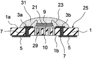
도 1 은, 종래의 발광 다이오드 패키지의 예로서 특허문헌 1 의 도 2 를 옮겨 기재한 것이다. 발광 소자인 LED 칩 (LED 소자)(21) 의 바로 아래에 관통 도체 (서멀 비아)(10) 를 설치하고, 서멀 비아 (10) 위에 접착제 (29) 를 개재하여 LED 칩 (21) 을 장착한다. 또한, LED 로부터 기판 배후에 대한 낮은 열저항을 실현하기 위해서는 비교적 큰 직경의 비아가 필요하다. 또, 서멀 비아의 직경이 단일한 비아에 의하여 전달할 수 있는 열의 양을 제한하기 때문에, 서멀 비아는 보통 여러 개의 비아에 의하여 기판 중에 형성되게 된다.FIG. 1 transfers and describes FIG. 2 of
LTCC 는 통상적으로 유리 분말과 세라믹스 필러 (세라믹스 분말) 를 주성분으로 하는 원료 분말에 수지 등을 첨가하여 시트 형상으로 성형하고, 1000 ℃ 이하의 온도에서 소성하여 기판이 되는 것이다. 상기 시트 형상의 성형체는 그린 시트라고 하여, 필요에 따라 절단, 천공 등의 가공이 실시되고, 또 도체 페이스트를 이용하여 도체가 인쇄되고, 통상은 복수 장이 적층되어 소성된다.LTCC is usually formed into a sheet by adding a resin or the like to a raw material powder mainly composed of glass powder and ceramic filler (ceramic powder), and baking at a temperature of 1000 ° C. or lower to form a substrate. The sheet-shaped molded body is referred to as a green sheet, and processing such as cutting and drilling are performed as necessary, and a conductor is printed using a conductor paste, and a plurality of sheets are usually laminated and fired.
LTCC 는, 열전도율이 높은 은 도체나 구리 도체의 분말을 페이스트로 하여 그린 시트에 형성된 관통공에 매립하거나 하여 은 도체나 구리 도체의 분말과 동시에 소성하여 제조할 수 있기 때문에 방열성이 우수한 관통 도체 첨부 기판을 효율적으로 생산할 수 있다.Since LTCC can be produced by embedding silver conductor or copper conductor powder with high thermal conductivity as a paste in a through hole formed in a green sheet, and by firing simultaneously with the powder of silver conductor or copper conductor, the substrate with a through conductor having excellent heat dissipation properties Can be produced efficiently.
(특허문헌 1) : 일본 공개특허공보 2006-41230호(Patent Document 1): Japanese Unexamined Patent Publication No. 2006-41230
종래예로서 도 1 에 나타내는 바와 같은 LED 패키지 구조를 채용하는 경우, 후술하는 항절강도를 크게 하고자 하면, 서멀 비아는 동시 소성시에 LTCC 기판으로부터 돌출되어 볼록 형상부를 형성하기 때문에, LED 칩은 그 서멀 비아의 볼록 형상부에 접착제를 개재하여 장착되어 있다. 그러나, 서멀 비아의 볼록 형상부의 높이가 높으면 접착제를 많이 사용해야만 하여 열저항이 증가하게 된다. 따라서, 항절강도가 크고, 또한 서멀 비아의 볼록 형상부의 높이가 낮은 것이 요구되고 있다.In the case of adopting the LED package structure as shown in FIG. 1 as a conventional example, when increasing the strength of the later-described strength, the thermal via protrudes from the LTCC substrate at the time of simultaneous firing to form a convex shape. It is attached to the convex part of the thermal via via an adhesive agent. However, if the height of the convex portion of the thermal via is high, a large amount of adhesive must be used to increase the thermal resistance. Therefore, it is desired to have a high tensile strength and a low height of the convex portion of the thermal via.
본 발명은 이와 같은 문제를 해결할 수 있는 LED 패키지의 제공을 목적으로 한다.An object of the present invention is to provide an LED package that can solve such a problem.
본 발명은, 기판 상에 발광 다이오드 소자가 실장되어 있는 발광 다이오드 패키지로서, 기판이 몰 백분율 표시로 SiO2 를 57 ~ 65 %, B2O3 를 13 ~ 18 %, CaO 를 9 ~ 23 %, Al2O3 을 3 ~ 8 %, K2O 및 Na2O 중 적어도 어느 일방을 합계로 0.5 ~ 6 % 함유하는 유리 분말과 세라믹스 필러를 함유하는 유리 세라믹스 조성물을 소성하여 얻어진 것인 발광 다이오드 패키지를 제공한다.The present invention provides a light emitting diode package in which a light emitting diode element is mounted on a substrate, wherein the substrate has a molar percentage of 57 to 65% SiO 2 , 13 to 18% B 2 O 3 , 9 to 23% CaO, A light emitting diode package obtained by firing a glass ceramic composition containing a ceramic powder and a glass powder containing 3 to 8% of Al 2 O 3 and at least one of K 2 O and Na 2 O in total of 0.5 to 6% To provide.
또, 상기 발광 다이오드 패키지로서, 발광 다이오드 소자가 실장되어 있는 기판의 면과 대향하는 기판의 타방의 면에 히트 싱크가 형성되어 있고, 관통 도체로서, 그 위에 발광 다이오드 소자가 실장되어 있는 것의 적어도 1 개가 그 히트 싱크와 접속되어 있는 서멀 비아 (Thermal vias) 인 발광 다이오드 패키지, 즉 서멀 비아를 갖는 기판의 일방의 면 상의 발광 다이오드 소자와 기판의 타방의 면측에 형성된 히트 싱크가, 당해 기판 중에 형성된 적어도 1 개의 서멀 비아에 의하여 접속되어 있는 발광 다이오드 패키지로서, 기판이 몰 백분율 표시로 SiO2 를 57 ~ 65 %, B2O3 을 13 ~ 18 %, CaO 를 9 ~ 23 %, Al2O3 을 3 ~ 8 %, K2O + Na2O를 0.5 ~ 6 % 함유하는 유리 분말과 세라믹스 필러를 함유하는 유리 세라믹스 조성물을 소성하여 얻어진 것인 발광 다이오드 패키지를 제공한다.Further, at least one of the light emitting diode package in which a heat sink is formed on the other surface of the substrate facing the surface of the substrate on which the light emitting diode element is mounted, and the light emitting diode element is mounted thereon as a through conductor. A light emitting diode package in which dogs are thermal vias connected to the heat sink, i.e., a heat sink formed on one side of the substrate with the thermal vias and the heat sink formed on the other side of the substrate, at least A light emitting diode package connected by one thermal via, wherein the substrate has a mole percentage display of 57 to 65% SiO 2 , 13 to 18% B 2 O 3 , 9 to 23% CaO, and 2 to 3% Al 2 O 3 . 3 to 8%, by firing a glass ceramic composition containing a glass powder and a ceramics filler, which contains 0.5 ~ 6% K 2 O + Na 2 O of the light emitting diode package is obtained the The.
또한, 발광 다이오드 소자는 발광 다이오드 칩 또는 간단히 칩으로 기재하는 경우가 있고, 이 기판은 절연 기판으로 기재하는 경우가 있다.In addition, a light emitting diode element may be described as a light emitting diode chip or simply a chip, and this substrate may be described as an insulating substrate.
또, 상기 세라믹스 필러가 알루미나 분말인 상기 발광 다이오드 패키지를 제공한다. The present invention also provides the light emitting diode package in which the ceramic filler is alumina powder.
또한, 상기 세라믹스 필러가 알루미나 분말 및 지르코니아 분말을 함유하는 상기 발광 다이오드 패키지를 제공한다.In addition, the ceramic filler provides the light emitting diode package containing alumina powder and zirconia powder.
또, 기판의 항절강도가 250 ㎫ 이상인 상기 발광 다이오드 패키지를 제공한다.Further, the light emitting diode package having a break strength of the substrate of 250 MPa or more is provided.
또, 상기 서멀 비아의 도체가 발광 다이오드 소자가 실장되어 있는 기판의 면에서 돌출되어 있고, 그 돌출량이 5 ㎛ 이하인 상기 발광 다이오드 패키지, 즉 발광 다이오드 소자와 히트 싱크를 접속하고 있는 서멀 비아의 도체가, 발광 다이오드 소자가 탑재되어 있는 기판면으로부터 돌출되어 있고, 그 돌출량이 5 ㎛ 이하인 상기 발광 다이오드 패키지를 제공한다.Further, the conductor of the thermal via protrudes from the surface of the substrate on which the light emitting diode element is mounted, and the light emitting diode package having a protruding amount of 5 µm or less, that is, the conductor of the thermal via connecting the light emitting diode element and the heat sink. The light emitting diode package protrudes from the surface of the substrate on which the light emitting diode element is mounted, and has a protruding amount of 5 m or less.
본 발명에서의 기판 또는 LED 패키지는 칩을 마운트한 후, 칼집을 낸 부분을 절곡시키거나, 기판을 소성한 후 다이아몬드 지석으로 이른바 다이싱함으로써 절단한다. 이 때 함께 기판 자체가 균열되거나 칩핑 (결손) 이 발생되면 패키지가 파손되어 비용이 상승한다. 이 때문에 기판의 항절강도가 클 것, 전형적으로는 250 ㎫ 이상인 것이 요구된다. 또한, 항절강도는 통상적으로 알루미나 기판이 400 ㎫ , 질화알루미늄 기판이 300 ㎫ 이다.The substrate or LED package according to the present invention is cut by mounting the chip, bending the cut portion, or firing the substrate and then dicing into so-called diamond grindstones. At this time, if the substrate itself is cracked or chipping occurs, the package is broken and the cost is increased. For this reason, it is required that the tensile strength of a board | substrate is large, typically 250 Mpa or more. In addition, the tensile strength is usually 400 MPa for an alumina substrate and 300 MPa for an aluminum nitride substrate.
또, 본 발명에서의 기판은 내산성이 우수한 것인 점이 바람직하다. 그 이유는, 기판에는 도금 등이 실시되는 경우가 있고, 이를 위해 기판이 산성 도금액 등으로 처리되는 경우가 있기 때문이다.Moreover, it is preferable that the board | substrate in this invention is excellent in acid resistance. This is because the substrate may be subjected to plating or the like, and for this purpose, the substrate may be treated with an acidic plating solution or the like.
본 발명자는 몰% 표시로 SiO2 를 81.6 %, B2O3 을 16.6 %, K2O 를 1.8 % 함유하는 유리 (후출하는 예 15 의 유리) 의 분말과 알루미나 분말을 이용하여 LTCC 기판을 제작한 바, 내산성이 양호하고, 또 관통 도체가 크게 돌출되는 현상은 확인되지 않았으나, 항절강도는 작아, 190 ㎫ 인 것을 알아내었다.The inventors have used LTCC substrates using alumina powders and powders of glass (glass from Example 15) that contain 81.6% SiO 2 , 16.6% B 2 O 3 , and 1.8% K 2 O in mole percent. When produced, the phenomenon that acid resistance was good and a penetration conductor protruded largely was not confirmed, but it was found out that the tensile strength was small and it was 190 Mpa.
그래서, 상기 유리 조성에 CaO, 및 Al2O3 을 첨가한 바, 항절강도는 250 ㎫ 가 되어 강도를 향상시킬 수 있었다 (후출하는 예 13 의 유리). 이것은 유리의 결정화 경향이 강해졌기 때문으로 생각한다. 또한, 석출 결정상은 아노사이트인 것으로 생각한다.Thus, the glass composition of the CaO, and Al 2 O 3 was added the flexural bar, wherein a is 250 ㎫ was possible to improve the strength (after shipment of the glass in Example 13). This is considered to be because the crystallization tendency of glass became strong. In addition, the precipitation crystal phase is considered to be ananocite.
그러나, CaO, 및 Al2O3 을 첨가함으로써 관통 도체가 크게 돌출되는 현상이 나타났다.However, the addition of CaO and Al 2 O 3 showed a phenomenon in which the through conductor protruded greatly.
관통 도체의 돌출을 억제하기 위해서는, 관통 도체와 그린 시트의 소성에 의한 수축 거동의 매칭이 중요하다. 본 발명자는 원료 분말에 함유되는 유리의 조성에 소량의 알칼리 성분을 첨가함으로써, 수축 거동을 관통 도체에 접근하는 것에 성공하였다 (후출하는 예 10, 예 11, 및 예 12 의 유리).In order to suppress the protrusion of the through conductor, matching of the shrinkage behavior due to the firing of the through conductor and the green sheet is important. The present inventors have succeeded in approaching the through conductor with shrinkage behavior by adding a small amount of an alkali component to the composition of the glass contained in the raw material powder (glasses of Examples 10, 11, and 12 falling out).
그러나, 유리가 결정화 경향이 강한 경우에는 관통 도체의 돌출을 충분히 억제하기가 곤란하였다. 이것은, 유리가 결정화되는 것에 따른 체적 수축이 커서 관통 도체와의 수축 매칭이 곤란하기 때문인 것으로 생각한다.However, when glass had a strong crystallization tendency, it was difficult to sufficiently suppress the protrusion of the through conductor. This is considered to be because the volume shrinkage due to crystallization of the glass is so large that shrinkage matching with the through conductor is difficult.
본 발명자는 이상의 견지를 기초로 하여 항절강도를 높이면서, 관통 도체의 돌출량을 충분히 작게 할 수 있는 유리 조성을 찾아내어 본 발명에 이르렀다.The present inventors have found a glass composition which can sufficiently reduce the amount of protrusion of the through-conductor while increasing the tensile strength based on the above points.
본 발명에 의하면, 관통 도체의 돌출량이 충분히 작고, 강도와 방열성이 우수한 LED 패키지를 효율적으로 제조할 수 있다.According to the present invention, a protruding amount of the through conductor is sufficiently small, and an LED package excellent in strength and heat dissipation can be efficiently produced.
또, 실장 신뢰성을 향상시킬 수 있어 치수 정밀도가 높은 LED 패키지를 얻을 수 있게 된다.In addition, the mounting reliability can be improved, and an LED package with high dimensional accuracy can be obtained.
또, 내산성이 높은 LED 패키지를 얻을 수 있게 된다.In addition, an LED package having high acid resistance can be obtained.
또, 은 도체와 그린 시트를 동시에 소성하여 기판을 제작할 때, LTCC 기판에 휨 등의 변형이 발생되는 경우가 있다. 이것은 주로 은 도체 페이스트와 그린 시트의 소성에 의한 수축량이 상이하기 때문이고, 또한 유리 중으로 은 이온이 용출됨으로써 은 도체와 접하는 부분의 유리 조성이 변화하여 은 도체로부터 먼 부분과 은 도체에 접하는 부분에서 수축 거동이 상이한 결과가 되기 때문으로도 생각된다.Moreover, when baking a silver conductor and a green sheet simultaneously, and manufacturing a board | substrate, distortion, such as curvature, may arise in an LTCC board | substrate. This is mainly because the amount of shrinkage due to the firing of the silver conductor paste and the green sheet is different, and the glass composition of the portion in contact with the silver conductor changes due to the elution of silver ions into the glass, and thus the portion away from the silver conductor and in the portion in contact with the silver conductor. It is also considered that the shrinkage behavior results in different results.
본 발명에 의하면, 동시 소성시에 기판의 휨이 발생되어도 그 휨이 작은 LED 패키지를 얻을 수 있게 된다.According to this invention, even if the board | substrate warpage generate | occur | produces at the time of co-firing, LED package with small curvature can be obtained.
또, LTCC 의 원료 분말에 함유되는 유리와 은의 반응에 의하여 발색 (은 발색) 되는 경우가 있다. 이것은 은 도체로부터 유리 중에 용출된 은 이온이 그 후에 환원되어 콜로이드화하기 때문으로 생각된다.Moreover, color development (silver color development) may occur by reaction of glass and silver contained in the raw material powder of LTCC. This is considered to be because silver ions eluted from the silver conductor into the glass are subsequently reduced to colloid.
본 발명에 의하면, 은 도체와 동시에 소성했을 때에 은 발색이 일어나지 않거나 또는 일어나기 어렵고, 기판의 반사율을 높일 수 있거나 또는 기판의 착색을 억제할 수 있다.According to the present invention, silver firing does not occur or hardly occurs when firing at the same time as the silver conductor, and the reflectance of the substrate can be increased or the coloring of the substrate can be suppressed.
도 1 은 종래의 발광 다이오드 패키지의 단면도이다.1 is a cross-sectional view of a conventional light emitting diode package.
이하, 본 발명의 실시형태에 대해 설명하는데, 본 발명은 이들에 한정되지 않는다.EMBODIMENT OF THE INVENTION Hereinafter, although embodiment of this invention is described, this invention is not limited to these.
본 발명에서의 유리 세라믹스 조성물 (이하, 간단히 본 발명의 조성물이라고 한다) 은 통상적으로 상기 유리 (이하, 본 발명의 조성물에 사용되는 이 유리를 본 발명의 유리라고 한다) 의 분말과 세라믹스 필러 (전형적으로는 알루미나 필러 즉 알루미나 분말이다) 를 함유하고, 또는 이것들로 이루어지는 그린 시트화하여 사용된다.The glass ceramic composition (hereinafter simply referred to as the composition of the present invention) in the present invention is usually a powder of ceramic (hereinafter referred to as the glass of the present invention) and a ceramic filler (typically referred to as the glass of the present invention). As an alumina filler, that is, an alumina powder), it is used, being made into the green sheet which consists of these, or these.
본 발명에 있어서, 그린 시트의 제조는 바람직하게는 아래와 같이 행해진다. 즉, 먼저 본 발명의 조성물과 폴리비닐부티랄, 아크릴 수지 등의 수지를 필요에 따라 프탈산디부틸, 프탈산디옥틸, 프탈산부틸벤질 등의 가소제 등도 첨가하여 혼합한다. 다음으로, 톨루엔, 자일렌, 부탄올 등의 용제를 첨가하여 슬러리로 하고, 폴리에틸렌테레프탈레이트 등의 필름 위에 닥터 블레이드법 등으로 이 슬러리를 시트 형상으로 성형한다. 마지막으로, 이 시트 형상으로 성형된 것을 건조시켜 용제를 제거하고 그린 시트로 한다.In the present invention, production of the green sheet is preferably performed as follows. That is, first, the composition of this invention, resins, such as a polyvinyl butyral and an acrylic resin, are also added and mixed as needed, plasticizers, such as dibutyl phthalate, dioctyl phthalate, and butyl benzyl phthalate. Next, a solvent such as toluene, xylene, butanol is added to form a slurry, and the slurry is molded into a sheet shape on a film such as polyethylene terephthalate by a doctor blade method or the like. Finally, what was molded in this sheet form is dried, a solvent is removed, and it is set as a green sheet.
상기 그린 시트에는 필요에 따라 은 페이스트, 은 도체 등을 사용하여 스크린 인쇄 등에 의하여 배선 패턴이나 관통 도체인 비아 등이 형성된다.If necessary, the green sheet is formed with a wiring pattern, vias, or the like, through screen printing using silver paste, silver conductor, or the like.
본 발명의 유리는 발광 다이오드 패키지 기판용 유리로서 바람직하다.The glass of this invention is suitable as glass for light emitting diode package substrates.
상기 그린 시트는, 소성 후 원하는 형상으로 가공하여 기판으로 한다. 이 경우, 피소성체는 1 장 또는 복수 장의 동일한 그린 시트를 중첩시킨 것이다. 또한, 이 기판은 본 발명의 LED 패키지용 기판으로서, 상기 소성은 전형적으로는 850 ~ 900 ℃ 에서 20 ~ 60 분간 유지하여 행해진다. 보다 전형적인 소성 온도는 860 ~ 880 ℃ 이다.The green sheet is processed into a desired shape after firing to form a substrate. In this case, the to-be-baked body superimposed one or more sheets of the same green sheet. In addition, this board | substrate is a board | substrate for LED packages of this invention, The said baking is typically performed by hold | maintaining for 20 to 60 minutes at 850-900 degreeC. More typical firing temperatures are from 860 ° C to 880 ° C.
또한, 은 페이스트 등과 동시에 소성하여 배선 패턴이나 관통 도체를 소성체 즉 기판의 내부에 형성하는 경우, 소성 온도는 880 ℃ 이하인 것이 바람직하다. 소성 온도가 880 ℃ 를 초과하는 경우에는 소성시에 은 또는 은 함유 도체가 연화되어 배선 패턴이나 관통 도체의 형상을 유지할 수 없게 될 우려가 있어, 보다 바람직하게는 870 ℃ 이하이다.Moreover, when baking simultaneously with silver paste etc. and forming a wiring pattern or a through conductor in a baking body, ie, a board | substrate, it is preferable that baking temperature is 880 degreeC or less. When the firing temperature exceeds 880 ° C, the silver or silver-containing conductor may soften during firing and may not be able to maintain the shape of the wiring pattern or the through conductor, more preferably 870 ° C or less.
본 발명의 조성물은, 900 ℃ 이하의 온도에서 소성해도 치밀한 소성체가 얻어지는 것이 바람직하다. 이와 같은 것이면, 은 페이스트 등의 도체 재료와 900 ℃ 이하의 온도에서 동시 소성할 수 있다.It is preferable that a compact fired body is obtained even if the composition of the present invention is fired at a temperature of 900 ° C or lower. If it is such a thing, it can bake simultaneously with conductor materials, such as silver paste, at the temperature of 900 degrees C or less.
본 발명의 조성물은, 질량 백분율 표시로 본 발명의 유리 분말을 25 ~ 55 %, 세라믹스 필러를 45 ~ 75 % 함유하는 것이 바람직하다. 본 발명의 유리 분말의 함유량이 25 % 미만이면 소성에 의하여 치밀한 소성체를 얻기가 곤란해질 우려가 있어, 바람직하게는 35 % 이상이다. 또, 유리 분말의 함유량이 55 % 를 초과하면 강도가 부족할 우려가 있어, 바람직하게는 50 % 이하, 보다 바람직하게는 45 % 이하이다.It is preferable that the composition of this invention contains 25 to 55% of glass powder of this invention and 45 to 75% of ceramic fillers by mass percentage display. When content of the glass powder of this invention is less than 25%, there exists a possibility that it may become difficult to obtain a compact plastic body by baking, Preferably it is 35% or more. Moreover, when content of glass powder exceeds 55%, there exists a possibility that intensity | strength may run short, Preferably it is 50% or less, More preferably, it is 45% or less.
세라믹스 필러는 기판의 강도를 높이는 성분이다. 그 함유량은 보다 바람직하게는 50 % 이상, 특히 바람직하게는 55 % 이상이다. 세라믹스 필러의 함유량이 75 % 를 초과하면, 소성에 의하여 치밀한 소성체를 얻기가 곤란해지거나 또는 기판 표면의 평활성이 손상될 우려가 있어, 바람직하게는 65 % 이하이다.The ceramic filler is a component that increases the strength of the substrate. The content is more preferably 50% or more, particularly preferably 55% or more. When the content of the ceramic filler exceeds 75%, it is difficult to obtain a compacted plastic body by firing or the smoothness of the substrate surface may be impaired, and preferably 65% or less.
본 발명의 조성물은, 본 발명의 목적을 해치지 않는 범위에서 그 밖의 성분으로서 무기물 분말, 예를 들어 내열 안료 등을 함유할 수 있다. 이 경우, 당해 그 밖의 성분의 함유량은 전형적으로는 합계로 5 % 이하이다.The composition of this invention can contain an inorganic powder, for example, a heat-resistant pigment, etc. as another component in the range which does not impair the objective of this invention. In this case, content of the said other components is 5% or less in total typically.
본 발명의 조성물 성분인 세라믹스 필러는 전형적으로는 알루미나 분말이다. 알루미나 분말을 함유함으로써 기판의 강도를 높일 수 있다. 기판의 강도를 높이기 위해서는 알루미나 분말을 30 % 이상 함유하는 것이 바람직하다.The ceramic filler which is a composition component of the present invention is typically an alumina powder. By containing alumina powder, the strength of the substrate can be increased. In order to increase the strength of the substrate, it is preferable to contain 30% or more of alumina powder.
또, 후술하는 기판의 반사율을 특히 높이고자 하는 경우에는, 본 발명의 조성물은 굴절률이 2 를 초과하는 고굴절률 세라믹스 분말을 함유하는 것이 보다 바람직하다. 고굴절률 세라믹스로서는, 예를 들어 티타니아, 지르코니아를 들 수 있다. 반사율을 높이고자 하는 경우에는, 지르코니아 분말의 함유량은 5 % 이상인 것이 바람직하고, 10 % 이상인 것이 보다 바람직하다. 이 경우, 알루미나 분말을 30 % 이상 함유하는 것이 바람직하다.Moreover, when it is going to especially raise the reflectance of the board | substrate mentioned later, it is more preferable that the composition of this invention contains the high refractive index ceramic powder whose refractive index exceeds 2. As high refractive index ceramics, titania and zirconia are mentioned, for example. In the case of increasing the reflectance, the content of the zirconia powder is preferably 5% or more, and more preferably 10% or more. In this case, it is preferable to contain 30% or more of alumina powder.
세라믹스 필러의 50 % 입경 (D50) 은 0.5 ~ 5 ㎛ 인 것이 바람직하다. D50 이 0.5 ㎛ 미만인 경우에는, 예를 들어 그린 시트 중에 분말을 균일하게 분산시키기가 곤란해지거나 또는 분말이 응집되기 쉬워져 취급하기가 어려워진다. D50 은 보다 바람직하게는 1 ㎛ 이상이다. D50 이 5 ㎛ 를 초과하는 경우에는 치밀한 소성체를 얻기 어려워지고, 보다 바람직하게는 3 ㎛ 이하이다.50% particle size (D 50) of the ceramics filler is preferably 0.5 ~ 5 ㎛. D becomes 50 are liable to be less than 0.5 ㎛ include, for example, or it is difficult to uniformly disperse the powder in the green sheet or powder agglomeration becomes difficult to handle. D 50 is more preferably 1 µm or more. If D 50 exceeds 5 ㎛ has been difficult to obtain a dense sintered body, and more preferably not more than 3 ㎛.
본 발명의 조성물 성분인 본 발명의 유리 분말은 통상적으로 용융 법에 의하여 얻어진 유리를 분쇄하여 제조된다. 분쇄 방법은, 본 발명의 목적을 해치지 않는 것이면 한정되지 않으며, 건식 분쇄이어도 되고 습식 분쇄이어도 된다. 습식 분쇄의 경우에는 용매로서 물을 사용하는 것이 바람직하다. 또 분쇄에는 롤 밀, 볼 밀, 제트 밀 등의 분쇄기를 적절히 사용할 수 있다. 유리는 분쇄 후에 필요에 따라서 건조되고 분급된다.The glass powder of this invention which is a composition component of this invention is normally manufactured by pulverizing the glass obtained by the melting method. The grinding method is not limited as long as it does not impair the object of the present invention, and may be dry grinding or wet grinding. In the case of wet grinding, it is preferable to use water as a solvent. Moreover, grinders, such as a roll mill, a ball mill, and a jet mill, can be used suitably for grinding | pulverization. The glass is dried and classified as needed after grinding.
본 발명의 조성물 성분인 본 발명의 유리 분말의 D50 은 0.5 ~ 5 ㎛ 인 것이 바람직하다. D50 이 0.5 ㎛ 미만인 경우에는, 예를 들어 그린 시트 중에 유리 분말을 균일하게 분산시키기 곤란해지고, 또 분말이 잘 응집되지 않아 취급하기가 어려워진다. D50 은 보다 바람직하게는 1 ㎛ 이상이다. D50 이 5 ㎛ 를 초과하는 경우에는 치밀한 소성체를 얻기 어려워지고, 보다 바람직하게는 3㎛ 이하이다.D 50 of the glass powder of the present invention] The ingredients of the present invention is preferably 0.5 ~ 5 ㎛. D 50 is less than 0.5 ㎛ include, for example, is difficult to uniformly disperse the glass powder in the green sheet, and is difficult to handle the powder has not been well agglomerated. D 50 is more preferably 1 µm or more. If D 50 exceeds 5 ㎛ has been difficult to obtain a dense sintered body, and more preferably not more than 3㎛.
본 발명에 있어서의 기판에는, 방열 등의 목적에서 1 개 이상의 관통 도체가 형성되어 있고, 그 관통 도체의 적어도 1 개 위에 LED 소자가 실장되어 있다.The board | substrate in this invention is formed with one or more through conductors for the purpose of heat dissipation, etc., and LED element is mounted on at least one of the through conductors.
그리고, 통상적으로 그 관통 도체는 열전도율이 높은 은이 주성분인 은 도체로 이루어지고, 동시 소성은 900 ℃ 이하에서 행해지는 것이 바람직하다. 은 도체가 사용되는 것은, 은이 열전도율이 높아 방열성이 우수하기 때문이다.In general, the through conductor is preferably composed of a silver conductor whose main component is silver having high thermal conductivity, and simultaneous firing is preferably performed at 900 ° C or lower. A silver conductor is used because silver has high thermal conductivity and is excellent in heat dissipation.
관통 도체는, 전형적으로는 상기 그린 시트의 소정 위치에 구멍을 형성하여 은 페이스트 등 도체 페이스트를 충전시킨 것을 적층하여 소성하는 방법으로 형성할 수 있다. 이 경우, 관통 도체 및 그것을 형성하기 위한 도체 페이스트는, 열전도율을 높이기 위하여 도체 이외의 무기 성분을 함유하지 않는 것이 바람직하다.The through-conductor can be formed by a method of forming a hole in a predetermined position of the green sheet and laminating and packing a conductor paste such as silver paste. In this case, it is preferable that the through conductor and the conductor paste for forming the same do not contain inorganic components other than the conductor in order to increase the thermal conductivity.
본 발명의 기판의 발광 소자 탑재부에 서멀 비아가 형성되는 경우, 서멀 비아의 도체는 발광 다이오드 소자가 실장되어 있는 면에서 돌출되어 있는 것이 바람직하다. 서멀 비아의 도체가 기판 표면에 대해 오목하게 되어 있으면, 서멀 비아의 도체와 발광 다이오드 소자 사이에 간극이 발생하거나 또는 접착제층이 두꺼워져, 발광 다이오드 소자로부터의 열을 서멀 비아의 도체에 효율적으로 방출할 수 없게 되기 때문이다. 서멀 비아의 도체 돌출량은 0 ~ 5 ㎛ 인 것이 바람직하다. 돌출량이 5 ㎛ 를 초과하여 서멀 비아의 도체가 크게 볼록해지면, 발광 다이오드 소자와 기판 사이에 간극이 발생하여 다량의 접착제를 사용하기 때문에 방열성이 저하된다, 또 실장할 때에 발광 다이오드 소자가 경사지게 되어, 소정 위치에 장착하기 어려워지는 경우가 있기 때문이다.When the thermal via is formed in the light emitting element mounting portion of the substrate of the present invention, the conductor of the thermal via is preferably protruded from the surface where the light emitting diode element is mounted. If the conductor of the thermal via is concave to the surface of the substrate, a gap is generated between the conductor of the thermal via and the light emitting diode element, or the adhesive layer is thickened, thereby efficiently dissipating heat from the light emitting diode element to the conductor of the thermal via. Because you can not. It is preferable that the conductor protrusion amount of a thermal via is 0-5 micrometers. If the amount of protrusion exceeds 5 μm and the conductor of the thermal via becomes largely convex, a gap is generated between the light emitting diode element and the substrate, so that a large amount of adhesive is used, so that the heat dissipation is deteriorated. It is because it may become difficult to attach to a predetermined position.
본 발명의 유리의 유리 전이점 (Tg) 은 550 ~ 700 ℃ 인 것이 바람직하다. Tg 가 550 ℃ 미만이면 그린 시트 중의 유기체 바인더 (수지) 를 제거하기 어려워지고, 700 ℃ 를 초과하면 소성시의 수축 개시 온도가 높아져 절연 기판의 치수 정밀도가 저하될 우려가 있다.It is preferable that the glass transition point (Tg) of the glass of this invention is 550-700 degreeC. When Tg is less than 550 degreeC, it becomes difficult to remove the organic binder (resin) in a green sheet, and when it exceeds 700 degreeC, the shrinkage start temperature at the time of baking becomes high and there exists a possibility that the dimensional precision of an insulating substrate may fall.
본 발명의 유리는, 전형적으로는 850 ~ 900 ℃ 에서 소성했을 때에 분상 (分相) 이 발생되는 것인 것이 바람직하다. 분상이 발생되는 것이 아니면, 소성체의 기계적 강도가 낮아질 우려가 있다. 또한, 여기서 말하는 분상이 발생되는 것이란, X 선 회절에 의하여 결정을 검출하는 것은 곤란하지만, 고분해능의 전자선 현미경으로 관찰했을 때 화학 조성이 상이한 상의 존재를 확인할 수 있는 것이 전형적이다.It is preferable that the glass of this invention generate | occur | produces powder phase typically when it bakes at 850-900 degreeC. If powder phase does not occur, there exists a possibility that the mechanical strength of a fired body may become low. In addition, although it is difficult to detect a crystal | crystallization by X-ray diffraction that the powdery phase here generate | occur | produces, it is typical that the presence of a phase with a different chemical composition can be confirmed when observed with a high-resolution electron beam microscope.
다음으로, 본 발명의 유리 성분에 대해 설명한다. 또한, 이하에서는 특별히 언급하지 않는 한 유리 조성은 몰 백분율로 표시한다.Next, the glass component of this invention is demonstrated. In addition, below, a glass composition is represented by mole percentage unless there is particular notice.
SiO2 는 유리의 네트워크 포머로서 필수적이다. SiO2 가 57 % 미만인 경우에는 안정된 유리를 얻기가 어려워지거나, 또는 화학적 내구성이 저하된다. 내산성을 높이고자 하는 경우 등에는, SiO2 는 바람직하게는 58 % 이상, 보다 바람직하게는 59 % 이상, 특히 바람직하게는 60 % 이상이다. SiO2 가 65 % 를 초과하는 경우에는 유리 용융 온도 또는 Tg 가 지나치게 높아질 우려가 있어, 바람직하게는 64 % 이하, 보다 바람직하게는 63 % 이하이다.SiO 2 is essential as the network former of the glass. When SiO 2 is less than 57%, it becomes difficult to obtain stable glass or the chemical durability is lowered. SiO 2 is preferably at least 58%, more preferably at least 59%, particularly preferably at least 60%, in order to increase acid resistance. When SiO 2 is more than 65% there is a fear that there is a glass melting temperature or Tg is too high, preferably 64% or less, more preferably 63% or less.
B2O3 은 유리의 네트워크 포머로서 필수적이다. B2O3 이 13 % 미만인 경우에는 유리 용융 온도 또는 Tg 가 지나치게 높아질 우려가 있어, 바람직하게는 14 % 이상, 보다 바람직하게는 15 % 이상이다. B2O3 이 18 % 를 초과하는 경우에는 안정된 유리를 얻기가 어려워지거나, 또는 화학적 내구성이 저하될 우려가 있어, 바람직하게는 17 % 이하, 보다 바람직하게는 16 % 이하이다.B 2 O 3 is essential as the network former of the glass. If B 2 O 3 is less than 13%, there is there is a fear that the glass melting temperature or Tg is too high, preferably not less than 14%, more preferably at least 15%. When B 2 O 3 exceeds 18% or is difficult to obtain a stable glass, or there is a fear that the chemical durability is reduced, and preferably 17%, more preferably not more than 16%.
Al2O3 은 유리의 안정성, 화학적 내구성 또는 강도를 높이는 성분으로서 필수적이다. Al2O3 이 3 % 미만인 경우에는 유리가 불안정해지고, 바람직하게는 4 % 이상, 보다 바람직하게는 5 % 이상이다. Al2O3 이 8 % 를 초과하는 경우에는 유리 용융 온도 또는 Tg 가 지나치게 높아져 바람직하게는 7 % 이하, 보다 바람직하게는 6 % 이하이다.Al 2 O 3 is essential as a component to enhance the stability, chemical durability or strength of the glass. If Al 2 O 3 is less than 3%, the glass becomes unstable, is, preferably, more preferably 4% or more is 5% or more. When Al 2 O 3 is more than 8% and preferably higher the glass melting temperature or Tg is over 7%, more preferably 6% or less.
CaO 는 유리를 안정화시키고, 유리 용융 온도를 저하시키고, 또한 소성시에 결정을 석출하기 용이하게 하는 성분으로서 필수적이고, 또한 유리의 Tg 를 저하시키는 경우도 있다. CaO 가 9 % 미만인 경우에는 유리 용융 온도가 지나치게 높아질 우려가 있어, 바람직하게는 10 % 이상이다. 유리를 쉽게 용융시키고자 하는 경우 등에는, CaO 는 바람직하게는 12 % 이상, 보다 바람직하게는 13 % 이상, 특히 바람직하게는 14 % 이상이다. CaO 가 23 % 를 초과하는 경우에는 유리가 불안정해질 우려가 있어, 바람직하게는 22 % 이하, 보다 바람직하게는 21 % 이하, 특히 바람직하게는 20 % 이하, 전형적으로는 18 % 이하이다.CaO is essential as a component which stabilizes glass, lowers glass melting temperature, and makes it easy to precipitate crystal | crystallization at the time of baking, and may also reduce Tg of glass. When CaO is less than 9%, there exists a possibility that glass melting temperature may become high too much, Preferably it is 10% or more. CaO is preferably at least 12%, more preferably at least 13%, particularly preferably at least 14% when the glass is to be easily melted or the like. When CaO exceeds 23%, there exists a possibility that glass may become unstable, Preferably it is 22% or less, More preferably, it is 21% or less, Especially preferably, it is 20% or less, and typically 18% or less.
Na2O 및 K2O 는 Tg 를 저하시키는 성분으로서, 적어도 어느 한쪽을 함유해야 한다. 그 합계 (Na2O + K2O) 가 0.5 % 미만인 경우에는, 유리 용융 온도 또는 Tg 가 지나치게 높아질 우려가 있어, 바람직하게는 0.8 % 이상이다. Na2O + K2O 의 합계량이 6 % 를 초과하는 경우에는 화학적 내구성, 특히 내산성이 악화될 우려가 있거나, 또는 소성체의 전기 절연성이 저하할 우려가 있어, 바람직하게는 5 % 이하, 보다 바람직하게는 4 % 이하이다.Na 2 O and K 2 O are components that lower Tg and should contain at least either. If the total (Na 2 O + K 2 O ) is less than 0.5%, the there is a possibility that the glass melting temperature or Tg is too high, preferably not less than 0.8%. When the total amount of Na 2 O + K 2 O exceeds 6%, chemical durability, in particular, acid resistance may be deteriorated, or electrical insulation of the fired body may be deteriorated, and preferably 5% or less. Preferably it is 4% or less.
관통 도체가 볼록한 형상이 되는 것을 방지 또는 억제하고자 하는 경우, 혹은 강도 또는 화학적 내구성을 높이고자 하는 경우 등에는 CaO 를 17 % 이하, Al2O3 을 4 ~ 7 몰%, K2O 및 Na2O 의 합계를 4 % 이하로 하는 것이 바람직하다.In order to prevent or suppress the through conductor from becoming convex, or to increase the strength or chemical durability, CaO is 17% or less, Al 2 O 3 is 4-7 mol%, K 2 O and Na 2 It is preferable to make the total of O into 4% or less.
본 발명의 유리는 본질적으로 상기 성분으로 이루어지나, 본 발명의 목적을 저해하지 않는 범위에서 그 밖의 성분을 함유해도 된다. 당해 그 밖의 성분을 함유하는 경우, 이들 성분의 함유량 합계는 10 % 이하인 것이 바람직하다.Although the glass of this invention consists essentially of the said component, you may contain other components in the range which does not impair the objective of this invention. When it contains the said other component, it is preferable that the sum total of content of these components is 10% or less.
예를 들어, 유리 융액의 점성을 저하시키는 등의 목적에서 TiO2 를 함유해도 되는 경우가 있고, 그 경우의 TiO2 의 함유량은 3 % 이하인 것이 바람직하다. 또, 유리의 안정성을 향상시키는 등의 목적에서 ZrO2 를 함유해도 되는 경우가 있어, 그 경우의 ZrO2 의 함유량은 3 % 이하인 것이 바람직하다.For example, it is preferable that the content of the can, in that case may contain a case where TiO 2 for the purpose, such as to lower the viscosity of the glass melt TiO 2 is not more than 3%. In addition, it is preferable that the content of the, in that case it may contain a case where ZrO 2 on the purpose of improving the stability of the glass ZrO 2 is not more than 3%.
또한, 본 발명의 유리는 납 산화물은 함유하지 않는 것이 바람직하다.Moreover, it is preferable that the glass of this invention does not contain lead oxide.
실시예 Example
이하에서, 본 발명의 실시예에 의하여 보다 더 상세하게 설명하지만, 본 발명은 이들에 한정하여 해석되는 것은 아니다.Hereinafter, although an Example of this invention is demonstrated in more detail, this invention is limited to these and is not interpreted.
표 1 의 예 1 ~ 6, 및 표 2 의 예 10 ~ 15 에서는, SiO2 로부터 ZrO2 까지의 란에 몰% 로 나타내는 조성이 되도록 원료를 조제, 혼합하고, 이 혼합된 원료를 백금 도가니에 넣고 1550 ~ 1600 ℃ 에서 60 분간 용융한 후, 용융 유리를 흘려서 냉각시켰다. 얻어진 유리를, 알루미나제의 볼 밀로 에틸알코올을 용매로 하여 20 ~ 60 시간 분쇄하여 유리 분말을 얻었다.In the example 1-6, and the example of Table 2, 10 to 15 in Table 1, to prepare, mix the raw materials so that the composition shown in mol% in the column to ZrO 2 from the SiO 2 and into the mixed raw material in a platinum crucible. After melting for 60 minutes at 1550-1600 degreeC, the molten glass was poured and cooled. The obtained glass was pulverized for 20 to 60 hours using ethyl alcohol as a solvent with a ball mill made of alumina to obtain a glass powder.
예 1 ~ 6 은 본 발명의 실시예이고, 예 10 ~ 15 는 비교예이다. 예 7 ~ 9 도 본 발명의 실시예이지만, 앞서 언급한 유리 분말의 제조는 실시하지 않았다.Examples 1-6 are Examples of this invention, and Examples 10-15 are comparative examples. Examples 7 to 9 are also examples of the present invention, but the production of the aforementioned glass powder was not carried out.
각각의 유리 분말 (예 1 ~ 6, 및 예 10 ~ 15) 의 D50 (단위 : ㎛ ) 을 시마즈 제작소사 제작 SALD2100 을 사용하여 측정했을 때 모두 2.5 ㎛ 였다.Each of the glass powder (for example, 1-6, and Examples 10 ~ 15) D 50 (unit: ㎛) was a 2.5 ㎛ both as measured using Shimazu Production Sosa SALD2100 manufactured.
또, 각각의 유리 분말의 Tg (단위 : ℃), 및 연화점 Ts (단위 : ℃) 를, 마크사이언스사 제작 열분석 장치 (TG-DTA2000) 를 사용하여, 승온 속도 10 ℃/분의 조건에서 1000 ℃ 까지 각각 측정하였다. 표 중의 Tg, 및 Ts 의 란에 「*」으로 기재한 것은, 이들 방법에 의해서는 Tg 또는 Ts 를 측정할 수 없었다는 것을 나타낸다. 또한, 표 중에 괄호로 표시한 것은 조성에서 추정한 값으로, 후술하는 H 및 항절강도에 대해서도 동일하다.Moreover, Tg (unit: degreeC) of each glass powder, and softening point Ts (unit: degreeC) were made into 1000 by the temperature of 10 degreeC / min of temperature rising rate using Mark Science Corporation thermal analysis apparatus (TG-DTA2000). Each was measured to ℃. In the column of Tg and Ts in the table, "*" indicates that Tg or Ts could not be measured by these methods. In addition, it is the value estimated by the composition in parentheses in a table | surface, and the same is also the case about H mentioned later and strength of a clause.
질량 백분율 표시로, 각각의 유리 분말 40 % 와 쇼와 전공사 제조 알루미나 필러 AL-45H 를 60 % 의 비율로 혼합한 분말 50 g 에 유기 용제 (톨루엔, 자일렌, 2-프로판올, 2-부탄올을 질량비 4 : 2 : 2 : 1 로 혼합한 것) 15 g, 가소제 (프탈산디-2-에틸헥실) 2.5 g, 및 수지 (덴카사 제조 폴리비닐부티랄 PVK#3000K) 5 g 과 분산제 (비크케미사 제조 DISPERBYK180) 를 혼합하여 슬러리로 하였다. 이 슬러리를 PET 필름 위에 닥터 블레이드법으로 도포하고, 도막을 건조시켜 두께가 0.2 ㎜ 인 그린 시트를 얻었다.In the mass percentage display, an organic solvent (toluene, xylene, 2-propanol, 2-butanol) was added to 50 g of a powder mixed with 40% of each glass powder and 60% of alumina fillers AL-45H manufactured by Showa Denko. 15 g of mass ratios mixed at 2: 2: 1), plasticizer (di-2-ethylhexyl phthalate) 2.5 g, and resin (polyvinyl butyral PVK # 3000K manufactured by Denka Co., Ltd.) and dispersant (Vikke) Unmade DISPERBYK180) was mixed to obtain a slurry. This slurry was apply | coated on the PET film by the doctor blade method, the coating film was dried and the green sheet which is 0.2 mm in thickness was obtained.
비아 페이스트 (도체 페이스트) 는, 도전성 분말 (다이켄 화학 공업사 제조의 평균 입자경 5 ㎛ 의 구 형상 은 분말) 및 비히클 (에틸셀룰로오스) 을 질량비 85 : 15 의 비율로 조제하고, 고형분의 농도가 질량 백분율 표시로 85 % 가 되도록 용제 (![]()
![]()
상기에서 얻은 그린 시트에 천공기를 사용하여, 직경 0.3 ㎜ 의 구멍을 뚫어 비아홀을 형성하였다. 비아홀 내에, 스크린 인쇄법에 의하여 상기 조합 (調合) 으로 제조한 비아 페이스트를 충전하였다. 이어서, 얻어진 그린 시트를 6 장 적층하고, 550 ℃ 에서 5 시간 유지하여 수지 성분을 분해 제거한 후, 870 ℃ 에서 30 분 유지하여 소성을 실시하였다. 얻어진 소성체 (절연 기판) 를 전자현미경 (히타치 하이테크사 제조 S3000H) 에 의하여 관찰하고, 도체 비아 즉 관통 도체의 볼록 형상의 높이를 5 지점에서 계측하였다. 이들 5 지점의 계측 결과 평균치를 표 1 의 H 란에 나타낸다 (단위 : ㎛ ). H 는 5 ㎛ 이하인 것이 바람직하다. H 가 5 ㎛ 를 초과하는 경우에는 LED 칩을 실장할 때에 기울어져 버려 광량이 저하될 우려가 있다.A hole having a diameter of 0.3 mm was drilled into the green sheet obtained above to form a via hole. In the via hole, the via paste produced by the above combination was filled by the screen printing method. Subsequently, six obtained green sheets were laminated | stacked, hold | maintained at 550 degreeC for 5 hours, and the resin component was decomposed | disassembled and removed, it hold | maintained at 870 degreeC for 30 minutes, and baked. The obtained fired body (insulation board | substrate) was observed with the electron microscope (S3000H by Hitachi High-Tech Co., Ltd.), and the height of the convex shape of a conductor via, ie, a through conductor, was measured at five points. The measurement result average of these 5 points is shown in H column of Table 1 (unit: micrometer). It is preferable that H is 5 micrometers or less. When H exceeds 5 micrometers, when mounting an LED chip, it inclines and there exists a possibility that light quantity may fall.
항절강도는 다음과 같은 방법으로 측정하였다. 즉, 상기에서 얻어진 그린 시트를 6 장 적층하고, 550 ℃ 에서 5 시간 유지하여 수지 성분을 분해 제거한 후, 870 ℃ 에서 30 분 유지하는 소성을 실시하여 항절강도 측정용 소성체를 제조하였다. 이 소성체를 절단하여 두께가 약 0.85 ㎜, 폭이 5 ㎜ 인 길고 가는 형상으로 가공한 것 10 장을 사용하여 3 점 굽힘 강도를 측정하였다 (측정 장치 : 인스트론사 제조, INSTRON 8561). 스팬은 15 ㎜, 크로스 헤드 스피드는 0.5 cm/분으로 하였다. 이들 측정 결과를 표 1, 및 표 2 의 강도의 란에 나타낸다 (단위 : ㎫). 항절강도는 250 ㎫ 이상인 것이 바람직하다.Section strength was measured by the following method. That is, six green sheets obtained above were laminated | stacked, hold | maintained at 550 degreeC for 5 hours, the resin component was decomposed | disassembled, and baked was hold | maintained at 870 degreeC for 30 minutes, and the fired body for measuring a breakage strength was manufactured. The three-point bending strength was measured using 10 sheets of this fired body cut out and processed into a long thin shape having a thickness of about 0.85 mm and a width of 5 mm (measurement apparatus: INSTRON 8561, manufactured by Instron). The span was 15 mm and the crosshead speed was 0.5 cm / min. These measurement results are shown in the column of the strength of Table 1 and Table 2 (unit: Mpa). The tensile strength is preferably 250 MPa or more.


예 2 와 동일한 유리 분말과 상기 알루미나 분말 AL-45H 와 제일 희원소 화학 공업사 제조의 지르코니아 분말 HSY-3F-J 를, 표 3 의 유리 분말 란, 알루미나 분말 란, 지르코니아 분말 란에 질량 백분율 표시로 나타낸 비율로 혼합한 혼합 분말을 사용하여 상기와 동일한 방법으로 그린 시트를 제작하였다. 얻어진 그린 시트를 6 장 적층하여 550 ℃ 에서 5 시간 유지하여 수지 성분을 제거하였다. 그 후, 예 2A 는 885 ℃ 에서 30 분, 예 2B, 예 2C, 예 2D, 및 예 2E 는 875 ℃ 에서 30분 유지하는 소성을 실시하여 소성체를 제조하고, 상기 방법으로 항절강도를 측정하였다. 이들 측정 결과를 예 2 의 결과와 함께 표 3 의 강도의 란에 나타낸다 (단위 : ㎫ ). 이 결과로부터, 예 2의 유리를 이용해 항절강도를 250 ㎫ 이상으로 하고자 하는 경우에는, 본 발명의 조성물이 질량 백분율 표시로 유리 분말을 25 ~ 55 %, 세라믹스 필러를 45 ~ 75 % 함유하는 것이 바람직하다는 것을 알 수 있다.The ratio which showed the same glass powder as Example 2, the said alumina powder AL-45H, and the zirconia powder HSY-3F-J by the most rare element chemical industry company by mass percentage display in the glass powder column, alumina powder column, and zirconia powder column of Table 3 Green sheet was produced in the same manner as above using the mixed powder mixed with. Six obtained green sheets were laminated | stacked, it hold | maintained at 550 degreeC for 5 hours, and the resin component was removed. Thereafter, Example 2A was fired at 885 ° C. for 30 minutes, Example 2B, Example 2C, Example 2D, and Example 2E held at 875 ° C. for 30 minutes to prepare a fired body, and to measure the breakdown strength by the above method. It was. These measurement results are shown in the column of the intensity | strength of Table 3 with the result of Example 2 (unit: Mpa). From this result, when it is desired to have a breakdown strength of 250 MPa or more using the glass of Example 2, it is preferable that the composition of the present invention contains 25 to 55% of the glass powder and 45 to 75% of the ceramic filler in terms of mass percentage. It is understood that it is preferable.
또, 반사율은 다음과 같은 방법으로 측정하였다. 상기에서 얻어진 그린 시트를 적층하여 소성하고, 1 변이 30 ㎜ 정도인 정방형이고, 또한 두께가 300 ㎛ 정도인 각 소성체를 얻었다. 얻어진 소성체의 반사율을, 오션옵틱스사 제조 분광기 USB2000 와 오션옵틱스사 제조의 소형 적분구 ISP-RF 를 사용하여 측정하고, 황산바륨 표준판의 반사율을 100 으로 하여 광 파장 460 ㎚ 에 있어서의 반사율 (단위 : %) 을 산출하였다. 결과를 표 3 에 나타낸다.In addition, the reflectance was measured by the following method. The green sheets obtained above were laminated and fired to obtain respective fired bodies each having a square of about 30 mm and having a thickness of about 300 µm. The reflectance of the resulting fired body was measured using Ocean Optics' spectrometer USB2000 and Ocean Optics's compact integrating sphere ISP-RF, and the reflectance at light wavelength 460 nm with the reflectance of barium sulfate standard plate as 100. :%) Was calculated. The results are shown in Table 3.
기판의 두께를 얇게 하고자 하는 등의 사용 조건이 있는 경우, 반사율은 85 % 이상인 것이 바람직하다. 예 2C 에서는, 높은 반사율을 얻을 수 있었다. 반사율이 85 % 미만인 경우에는, 기판의 두께를 얇게 했을 때에 광의 누출이 커질 우려가 있다.In the case where there are use conditions such as thinning the thickness of the substrate, the reflectance is preferably 85% or more. In Example 2C, a high reflectance could be obtained. When the reflectance is less than 85%, there is a fear that light leakage increases when the thickness of the substrate is reduced.

산업상의 이용가능성Industrial availability
본 발명의 발광 다이오드 패키지는, 고휘도 (HB) 광 다이오드 백라이트, 디스플레이에 관련된 광원, 자동차 조명, 장식 조명, 표지 및 광고 조명, 및 정보 디스플레이 용도를 포함하는 조명 디바이스의 용도에 바람직하고, 특히 휴대전화나 대형 액정 TV 등의 백라이트에 이용할 수 있다.The light emitting diode package of the present invention is suitable for the use of lighting devices including high brightness (HB) photodiode backlights, light sources related to displays, automotive lighting, decorative lighting, signs and advertising lighting, and information display applications, and in particular mobile phones And backlights such as large liquid crystal TVs.
또한, 2008년 4월 18일에 출원된 일본 특허 출원 2008-108953호의 명세서, 특허 청구의 범위, 도면 및 요약서의 전체 내용을 여기에 인용하여, 본 발명의 명세서의 개시로서 도입한다.In addition, all the content of the JP Patent application 2008-108953, a claim, drawing, and the abstract for which it applied on April 18, 2008 is referred here, and it introduces as an indication of the specification of this invention.
1 : 절연 기판
1a, 1b : 주면 (主面)
3a, 3b : 접속 단자
5 : 외부 전극 단자
7 : 통전용 비아 도체
9 : 탑재부
10 : 서멀 비아 (관통 도체)
21 : LED 소자
23 : 본딩 와이어
25 : 발광 장치
29 : 접착제
31 : 몰드 재1: insulated substrate
1a, 1b: main surface
3a, 3b: connection terminal
5: external electrode terminal
7: Via Conductor for Electricity
9: mounting part
10: Thermal Via (Through Conductor)
21: LED device
23: bonding wire
25: light emitting device
29: adhesive
31: Mold Ash
Claims (13)
기판이 몰 백분율 표시로 SiO2 를 57 ~ 65 %, B2O3 을 13 ~ 18 %, CaO 를 9 ~ 23 %, Al2O3 을 3 ~ 8 %, K2O 및 Na2O 중 적어도 어느 일방을 합계로 0.5 ~ 6 % 함유하는 유리의 분말과 세라믹스 필러를 함유하는 유리 세라믹스 조성물을 소성하여 얻어진 것을 특징으로 하는 발광 다이오드 패키지.A light emitting diode package having a light emitting diode element mounted on a substrate,
Substrate indicates molar percentage of 57 to 65% SiO 2 , 13 to 18% B 2 O 3 , 9 to 23% CaO, 3 to 8% Al 2 O 3 , at least K 2 O and Na 2 O A light emitting diode package obtained by firing a glass ceramic composition containing a powder of a glass and a ceramic filler containing 0.5 to 6% in total either.
상기 유리의 SiO2 가 58 몰% 이상인, 발광 다이오드 패키지.The method of claim 1,
Wherein the SiO 2 of the glass is at least 58 mole percent.
상기 유리의 CaO 가 12 몰% 이상인, 발광 다이오드 패키지.The method according to claim 1 or 2,
Wherein the CaO of the glass is at least 12 mole percent.
상기 유리의, CaO 가 17 몰% 이하, Al2O3 이 4 ~ 7 몰%, K2O 및 Na2O 의 합계가 4 % 이하인, 발광 다이오드 패키지.The method according to any one of claims 1 to 3,
Of the glass, CaO are 17 mol% or less, Al 2 O 3 is 4-7 mol%, not more than the total of the K 2 O and Na 2 O 4%, the LED package.
상기 세라믹스 필러가 알루미나 분말인, 발광 다이오드 패키지. The method according to any one of claims 1 to 4,
The ceramic filler is alumina powder, the light emitting diode package.
상기 세라믹스 필러가 알루미나 분말 및 지르코니아 분말을 함유하는, 발광 다이오드 패키지.The method of claim 5, wherein
Wherein said ceramic filler contains alumina powder and zirconia powder.
상기 유리 세라믹스 조성물이 질량 백분율 표시로 상기 유리의 분말을 25 ~ 55 %, 상기 세라믹스 필러를 45 ~ 75 % 함유하는, 발광 다이오드 패키지.The method according to any one of claims 1 to 6,
A light emitting diode package, wherein the glass ceramic composition contains 25 to 55% of the powder of the glass and 45 to 75% of the ceramic filler in terms of mass percentage.
상기 유리 세라믹스 조성물이 질량 백분율 표시로 알루미나 분말을 30 % 이상 함유하는, 발광 다이오드 패키지.The method of claim 7, wherein
A light emitting diode package, wherein said glass ceramic composition contains at least 30% alumina powder in terms of mass percentage.
상기 유리 세라믹스 조성물이 질량 백분율 표시로 지르코니아 분말을 5 % 이상 함유하는, 발광 다이오드 패키지.The method of claim 8,
A light emitting diode package, wherein said glass ceramics composition contains at least 5% zirconia powder in terms of mass percentage.
상기 기판에 1 개 이상의 관통 도체가 형성되어 있고, 그 관통 도체의 적어도 1 개 위에 발광 다이오드 소자가 실장되어 있는, 발광 다이오드 패키지. The method according to any one of claims 1 to 9,
A light emitting diode package in which at least one through conductor is formed on the substrate, and a light emitting diode element is mounted on at least one of the through conductors.
발광 다이오드 소자가 실장되어 있는 기판의 면과 대향하는 기판의 타방의 면에 히트 싱크가 형성되어 있고, 관통 도체로서 그 위에 발광 다이오드 소자가 실장되어 있는 것의 적어도 1 개가 그 히트 싱크와 접속되어 있는 서멀 비아인, 발광 다이오드 패키지.The method of claim 10,
The heat sink is formed in the other surface of the board | substrate which opposes the surface of the board | substrate in which the light emitting diode element is mounted, and at least one of which the light emitting diode element is mounted as a through conductor is connected with the heat sink. Vias, LED package.
상기 서멀 비아의 도체가, 발광 다이오드 소자가 실장되어 있는 기판의 면에서 돌출되어 있고, 그 돌출량이 5 ㎛ 이하인, 발광 다이오드 패키지. The method of claim 11,
The conductor of said thermal via protrudes from the surface of the board | substrate in which the light emitting diode element is mounted, and the protrusion amount is 5 micrometers or less, The light emitting diode package.
기판의 항절강도가 250 ㎫ 이상인, 발광 다이오드 패키지.The method according to any one of claims 1 to 12,
The light emitting diode package having a breakdown strength of the substrate of 250 MPa or more.
Applications Claiming Priority (2)
| Application Number | Priority Date | Filing Date | Title |
|---|---|---|---|
| JPJP-P-2008-108953 | 2008-04-18 | ||
| JP2008108953 | 2008-04-18 |
Publications (1)
| Publication Number | Publication Date |
|---|---|
| KR20100135223A true KR20100135223A (en) | 2010-12-24 |
Family
ID=41199052
Family Applications (1)
| Application Number | Title | Priority Date | Filing Date |
|---|---|---|---|
| KR1020107017068A Ceased KR20100135223A (en) | 2008-04-18 | 2009-04-03 | Light emitting diode package |
Country Status (7)
| Country | Link |
|---|---|
| US (1) | US8309974B2 (en) |
| EP (1) | EP2267799A1 (en) |
| JP (2) | JP5061236B2 (en) |
| KR (1) | KR20100135223A (en) |
| CN (1) | CN102007609B (en) |
| TW (1) | TW201006012A (en) |
| WO (1) | WO2009128354A1 (en) |
Cited By (6)
| Publication number | Priority date | Publication date | Assignee | Title |
|---|---|---|---|---|
| US8822032B2 (en) | 2010-10-28 | 2014-09-02 | Corning Incorporated | Phosphor containing glass frit materials for LED lighting applications |
| US9011720B2 (en) | 2012-03-30 | 2015-04-21 | Corning Incorporated | Bismuth borate glass encapsulant for LED phosphors |
| US9202996B2 (en) | 2012-11-30 | 2015-12-01 | Corning Incorporated | LED lighting devices with quantum dot glass containment plates |
| US10017849B2 (en) | 2012-11-29 | 2018-07-10 | Corning Incorporated | High rate deposition systems and processes for forming hermetic barrier layers |
| US10158057B2 (en) | 2010-10-28 | 2018-12-18 | Corning Incorporated | LED lighting devices |
| US10439109B2 (en) | 2013-08-05 | 2019-10-08 | Corning Incorporated | Luminescent coatings and devices |
Families Citing this family (56)
| Publication number | Priority date | Publication date | Assignee | Title |
|---|---|---|---|---|
| US9082921B2 (en) * | 2007-10-31 | 2015-07-14 | Cree, Inc. | Multi-die LED package |
| US9172012B2 (en) | 2007-10-31 | 2015-10-27 | Cree, Inc. | Multi-chip light emitter packages and related methods |
| US9666762B2 (en) | 2007-10-31 | 2017-05-30 | Cree, Inc. | Multi-chip light emitter packages and related methods |
| JP5569942B2 (en) * | 2009-10-27 | 2014-08-13 | 学校法人東京理科大学 | Luminescent glass, light-emitting device provided with the luminescent glass, and method for producing the luminescent glass |
| WO2011059070A1 (en) * | 2009-11-13 | 2011-05-19 | 旭硝子株式会社 | Substrate for light-emitting elements and light-emitting device |
| KR100962706B1 (en) * | 2009-11-27 | 2010-06-15 | 주식회사 테크엔 | Manufacture method of the large illuminations with power led |
| US8927433B2 (en) * | 2009-12-18 | 2015-01-06 | Electronics And Telecommunications Research Institute | Conductive via hole and method for forming conductive via hole |
| US8174044B2 (en) * | 2010-01-14 | 2012-05-08 | Shang-Yi Wu | Light emitting diode package and method for forming the same |
| JP2011176303A (en) * | 2010-01-29 | 2011-09-08 | Asahi Glass Co Ltd | Substrate for mounting light emitting element and method for manufacturing the same |
| WO2011104963A1 (en) * | 2010-02-25 | 2011-09-01 | 旭硝子株式会社 | Substrate for mounting light emitting element, and light emitting device |
| TW201143152A (en) * | 2010-03-31 | 2011-12-01 | Asahi Glass Co Ltd | Substrate for light-emitting element and light-emitting device employing it |
| JP5596410B2 (en) * | 2010-05-18 | 2014-09-24 | スタンレー電気株式会社 | Semiconductor light emitting device |
| JP5655375B2 (en) * | 2010-05-31 | 2015-01-21 | 旭硝子株式会社 | Glass ceramic composition, light emitting diode element substrate and light emitting device. |
| WO2012005308A1 (en) * | 2010-07-07 | 2012-01-12 | 旭硝子株式会社 | Reflective frame for light-emitting elements, substrate for light-emitting elements, and light-emitting device |
| WO2012014853A1 (en) * | 2010-07-26 | 2012-02-02 | 旭硝子株式会社 | Substrate for light-emitting element, light-emitting device, and method for producing substrate for light-emitting element |
| JP5915527B2 (en) | 2010-07-29 | 2016-05-11 | 旭硝子株式会社 | Glass ceramic composition, substrate for light emitting element, and light emitting device |
| JP5725029B2 (en) * | 2010-09-17 | 2015-05-27 | 旭硝子株式会社 | Light emitting element mounting substrate and light emitting device |
| JP2012074478A (en) * | 2010-09-28 | 2012-04-12 | Asahi Glass Co Ltd | Substrate for light emitting element, and light emitting device |
| JP5888690B2 (en) * | 2010-11-08 | 2016-03-22 | 奥野製薬工業株式会社 | White ceramic color composition |
| US10267506B2 (en) | 2010-11-22 | 2019-04-23 | Cree, Inc. | Solid state lighting apparatuses with non-uniformly spaced emitters for improved heat distribution, system having the same, and methods having the same |
| US11101408B2 (en) * | 2011-02-07 | 2021-08-24 | Creeled, Inc. | Components and methods for light emitting diode (LED) lighting |
| US9704793B2 (en) * | 2011-01-04 | 2017-07-11 | Napra Co., Ltd. | Substrate for electronic device and electronic device |
| TW201251140A (en) | 2011-01-31 | 2012-12-16 | Cree Inc | High brightness light emitting diode (LED) packages, systems and methods with improved resin filling and high adhesion |
| TW201246619A (en) * | 2011-03-31 | 2012-11-16 | Asahi Glass Co Ltd | Substrate for light emitting element and light emitting device |
| TWI504030B (en) * | 2011-04-07 | 2015-10-11 | A co-fired ceramic substrate having a built-in heat radiating portion, and a light emitting diode having the substrate | |
| WO2013002348A1 (en) * | 2011-06-30 | 2013-01-03 | 旭硝子株式会社 | Light-emitting element substrate and light-emitting device |
| JP5937315B2 (en) * | 2011-08-11 | 2016-06-22 | シチズン電子株式会社 | Light emitting diode |
| CN102322580A (en) * | 2011-09-09 | 2012-01-18 | 福建省万邦光电科技有限公司 | LED (light-emitting diode) bulb light with high-whiteness substrate |
| CN102287663A (en) * | 2011-09-09 | 2011-12-21 | 福建省万邦光电科技有限公司 | Light emitting diode (LED) light source single-cup module for high-whiteness base plate |
| CN102290519A (en) * | 2011-09-09 | 2011-12-21 | 福建省万邦光电科技有限公司 | Substrate with high whiteness for packaging of LED (Light Emitting Diode) |
| CN102322581A (en) * | 2011-09-09 | 2012-01-18 | 福建省万邦光电科技有限公司 | LED (light-emitting diode) light source module with high-whiteness substrate |
| CN103035814A (en) * | 2011-10-10 | 2013-04-10 | 宁波瑞昀光电照明科技有限公司 | High heat dissipation aluminum substrate |
| TWI484674B (en) * | 2011-12-08 | 2015-05-11 | 新世紀光電股份有限公司 | Electronic component |
| JP5932494B2 (en) * | 2012-06-01 | 2016-06-08 | 日亜化学工業株式会社 | Light emitting element mounting substrate and light emitting device |
| KR20140021910A (en) * | 2012-08-13 | 2014-02-21 | 삼성전기주식회사 | Core substrate and printed circuit board using the same |
| JP2014037324A (en) * | 2012-08-13 | 2014-02-27 | Ariake Materials Co Ltd | Ceramics sintered compact for reflector |
| TWI550920B (en) * | 2012-12-13 | 2016-09-21 | 鴻海精密工業股份有限公司 | Light-emitting diode |
| JP6098200B2 (en) * | 2013-02-05 | 2017-03-22 | 旭硝子株式会社 | Light emitting element substrate and light emitting device |
| FR3003081A1 (en) * | 2013-03-07 | 2014-09-12 | Saint Gobain Rech | VITROCERAMIC MONTE SUPPORT FOR LED |
| JP6319947B2 (en) * | 2013-04-19 | 2018-05-09 | 日本特殊陶業株式会社 | Ceramic wiring board |
| JP6185864B2 (en) * | 2013-06-07 | 2017-08-23 | 本田技研工業株式会社 | Integrating sphere |
| JP2015106633A (en) * | 2013-11-29 | 2015-06-08 | 京セラ株式会社 | Substrate of light-emitting element mounting use, and light-emitting element module arranged by use thereof |
| CN103779285A (en) * | 2014-01-21 | 2014-05-07 | 中国兵器工业集团第二一四研究所苏州研发中心 | Heat dissipation packaging structure for hybrid integrated power module |
| TWI543315B (en) * | 2014-04-16 | 2016-07-21 | 光頡科技股份有限公司 | A carrier and a package structure having the carrier |
| JP6701566B2 (en) * | 2016-04-05 | 2020-05-27 | 日本電気硝子株式会社 | Composite powder, green sheet, light-reflecting substrate, and light-emitting device using these |
| US10658264B2 (en) * | 2017-09-01 | 2020-05-19 | Analog Devices, Inc. | Diamond-based heat spreading substrates for integrated circuit dies |
| DE102018121208B4 (en) * | 2017-09-01 | 2021-04-29 | Analog Devices, Inc. | Diamond-based heat distribution substrates for integrated circuit dies |
| JP2018019106A (en) * | 2017-10-23 | 2018-02-01 | 日本特殊陶業株式会社 | Ceramic wiring board |
| US10804180B2 (en) | 2017-11-30 | 2020-10-13 | Taiwan Semiconductor Manufacturing Co., Ltd. | Semiconductor device and method for manufacturing the same |
| CN113195435A (en) * | 2018-12-20 | 2021-07-30 | 株式会社村田制作所 | Glass ceramic material, laminate, and electronic component |
| JP7521430B2 (en) * | 2019-02-14 | 2024-07-24 | Agc株式会社 | Substrate for light emitting element and method for producing same |
| US11058883B2 (en) * | 2019-02-15 | 2021-07-13 | Medtronic, Inc. | Feedthrough assembly |
| FR3096831B1 (en) * | 2019-06-03 | 2021-06-18 | St Microelectronics Grenoble 2 | Electronic device comprising an electronic chip mounted above a support substrate |
| JP2023040431A (en) * | 2021-09-10 | 2023-03-23 | 山村フォトニクス株式会社 | glass ceramics substrate |
| CN113896513B (en) * | 2021-11-02 | 2022-10-04 | 珠海粤科京华科技有限公司 | High-performance alumina ceramic substrate and preparation method thereof |
| CN115565971B (en) * | 2022-10-26 | 2024-02-23 | 弘大芯源(深圳)半导体有限公司 | A chip packaging structure with good heat dissipation performance |
Family Cites Families (22)
| Publication number | Priority date | Publication date | Assignee | Title |
|---|---|---|---|---|
| JPS61186248A (en) * | 1985-02-13 | 1986-08-19 | Nippon Electric Glass Co Ltd | Glass ceramic |
| JP2800176B2 (en) * | 1987-08-18 | 1998-09-21 | 旭硝子株式会社 | Glass ceramic composition |
| JPH01252548A (en) * | 1987-12-28 | 1989-10-09 | Asahi Glass Co Ltd | Glass ceramic composition |
| JPH01226750A (en) * | 1988-03-04 | 1989-09-11 | Sumitomo Metal Mining Co Ltd | Inorganic composition for insulating paste |
| JPH0450141A (en) * | 1990-06-18 | 1992-02-19 | Hitachi Ltd | Glass-ceramic substrate |
| JP2000203879A (en) * | 1999-01-18 | 2000-07-25 | Sumitomo Metal Electronics Devices Inc | Glass ceramic substrate |
| WO2005106973A1 (en) * | 2004-04-27 | 2005-11-10 | Kyocera Corporation | Wiring board for light emitting element |
| JP4780939B2 (en) | 2004-07-28 | 2011-09-28 | 京セラ株式会社 | Light emitting device |
| DE102005000660A1 (en) * | 2005-01-04 | 2006-11-09 | Schott Ag | Lighting device with a structured body |
| DE102005000663B4 (en) * | 2005-01-04 | 2010-08-05 | Schott Ag | Process for clouding a glass, in particular a borosilicate glass, glass tube and its use |
| JP4947332B2 (en) * | 2005-01-28 | 2012-06-06 | 日立化成工業株式会社 | LED heat block and LED device using the same |
| US7550319B2 (en) * | 2005-09-01 | 2009-06-23 | E. I. Du Pont De Nemours And Company | Low temperature co-fired ceramic (LTCC) tape compositions, light emitting diode (LED) modules, lighting devices and method of forming thereof |
| JP4688633B2 (en) | 2005-10-27 | 2011-05-25 | 京セラ株式会社 | LIGHT REFLECTOR, LIGHT EMITTING ELEMENT WIRING BOARD, AND LIGHT EMITTING DEVICE |
| JP4688695B2 (en) | 2006-02-24 | 2011-05-25 | 京セラ株式会社 | LIGHT REFLECTOR, LIGHT EMITTING ELEMENT WIRING BOARD, AND LIGHT EMITTING DEVICE |
| JP4789671B2 (en) * | 2006-03-28 | 2011-10-12 | 京セラ株式会社 | WIRING BOARD FOR LIGHT EMITTING ELEMENT AND LIGHT EMITTING DEVICE |
| JP4814703B2 (en) * | 2006-06-20 | 2011-11-16 | 京セラ株式会社 | Circuit board |
| EP2317571A1 (en) * | 2008-08-21 | 2011-05-04 | Asahi Glass Company, Limited | Light-emitting device |
| JP5206770B2 (en) * | 2010-02-19 | 2013-06-12 | 旭硝子株式会社 | Light emitting element mounting substrate and light emitting device |
| TW201143152A (en) * | 2010-03-31 | 2011-12-01 | Asahi Glass Co Ltd | Substrate for light-emitting element and light-emitting device employing it |
| KR20110111243A (en) * | 2010-04-02 | 2011-10-10 | 아사히 가라스 가부시키가이샤 | Light emitting element mounting substrate and light emitting device using the substrate |
| JP2012009850A (en) * | 2010-05-26 | 2012-01-12 | Panasonic Corp | Hybrid substrate and manufacturing method therefor |
| CN102347426A (en) * | 2010-07-26 | 2012-02-08 | 旭硝子株式会社 | Substrate for mounting light-emitting element, production process thereof and light-emitting device |
-
2009
- 2009-04-03 KR KR1020107017068A patent/KR20100135223A/en not_active Ceased
- 2009-04-03 CN CN2009801137206A patent/CN102007609B/en active Active
- 2009-04-03 WO PCT/JP2009/056976 patent/WO2009128354A1/en not_active Ceased
- 2009-04-03 EP EP09733229A patent/EP2267799A1/en not_active Withdrawn
- 2009-04-03 JP JP2010508173A patent/JP5061236B2/en active Active
- 2009-04-06 TW TW098111369A patent/TW201006012A/en unknown
-
2010
- 2010-09-14 US US12/881,204 patent/US8309974B2/en active Active
-
2012
- 2012-07-31 JP JP2012169164A patent/JP5668730B2/en active Active
Cited By (8)
| Publication number | Priority date | Publication date | Assignee | Title |
|---|---|---|---|---|
| US8822032B2 (en) | 2010-10-28 | 2014-09-02 | Corning Incorporated | Phosphor containing glass frit materials for LED lighting applications |
| US10158057B2 (en) | 2010-10-28 | 2018-12-18 | Corning Incorporated | LED lighting devices |
| US9011720B2 (en) | 2012-03-30 | 2015-04-21 | Corning Incorporated | Bismuth borate glass encapsulant for LED phosphors |
| US9624124B2 (en) | 2012-03-30 | 2017-04-18 | Corning Incorporated | Bismuth borate glass encapsulant for LED phosphors |
| US10023492B2 (en) | 2012-03-30 | 2018-07-17 | Corning Incorporated | Bismuth borate glass encapsulant for LED phosphors |
| US10017849B2 (en) | 2012-11-29 | 2018-07-10 | Corning Incorporated | High rate deposition systems and processes for forming hermetic barrier layers |
| US9202996B2 (en) | 2012-11-30 | 2015-12-01 | Corning Incorporated | LED lighting devices with quantum dot glass containment plates |
| US10439109B2 (en) | 2013-08-05 | 2019-10-08 | Corning Incorporated | Luminescent coatings and devices |
Also Published As
| Publication number | Publication date |
|---|---|
| CN102007609B (en) | 2013-01-23 |
| JPWO2009128354A1 (en) | 2011-08-04 |
| WO2009128354A1 (en) | 2009-10-22 |
| JP2012229160A (en) | 2012-11-22 |
| EP2267799A1 (en) | 2010-12-29 |
| CN102007609A (en) | 2011-04-06 |
| JP5061236B2 (en) | 2012-10-31 |
| TW201006012A (en) | 2010-02-01 |
| JP5668730B2 (en) | 2015-02-12 |
| US20110001162A1 (en) | 2011-01-06 |
| US8309974B2 (en) | 2012-11-13 |
Similar Documents
| Publication | Publication Date | Title |
|---|---|---|
| KR20100135223A (en) | Light emitting diode package | |
| CN102030477B (en) | Ceramic material composition | |
| JP5429038B2 (en) | Light emitting element mounting substrate and light emitting device | |
| US8604499B2 (en) | Light-emitting device | |
| JP5915527B2 (en) | Glass ceramic composition, substrate for light emitting element, and light emitting device | |
| US20120018759A1 (en) | Substrate for mounting light-emitting element, production process thereof and light-emitting device | |
| CN102770977A (en) | Substrate for mounting light-emitting element and light-emitting device | |
| KR20120123023A (en) | Substrate for mounting light-emitting element, and light-emitting device | |
| JP2015120621A (en) | Glass ceramic composition, substrate for light emitting element, and light emitting device | |
| JPWO2012036219A1 (en) | Light emitting element substrate and light emitting device | |
| JP5720454B2 (en) | Light-emitting element mounting substrate, method for manufacturing the same, and light-emitting device | |
| US20120201037A1 (en) | Substrate for light-emitting element and light-emitting device | |
| JP5556336B2 (en) | Glass ceramic composition and element mounting substrate | |
| JP6150159B2 (en) | Glass ceramic for light emitting diode package, ceramic substrate using the same, and light emitting diode package | |
| JP5725029B2 (en) | Light emitting element mounting substrate and light emitting device | |
| JP2011258866A (en) | Substrate for mounting light emitting element and light emitting device | |
| JP2013239546A (en) | Substrate for mounting light emitting element and light emitting device | |
| JP2012238855A (en) | Substrate for light emitting element and light emitting device | |
| JP2015070088A (en) | Substrate for light-emitting element and light-emitting device |
Legal Events
| Date | Code | Title | Description |
|---|---|---|---|
| PA0105 | International application |
St.27 status event code: A-0-1-A10-A15-nap-PA0105 |
|
| PG1501 | Laying open of application |
St.27 status event code: A-1-1-Q10-Q12-nap-PG1501 |
|
| R18-X000 | Changes to party contact information recorded |
St.27 status event code: A-3-3-R10-R18-oth-X000 |
|
| A201 | Request for examination | ||
| PA0201 | Request for examination |
St.27 status event code: A-1-2-D10-D11-exm-PA0201 |
|
| E902 | Notification of reason for refusal | ||
| PE0902 | Notice of grounds for rejection |
St.27 status event code: A-1-2-D10-D21-exm-PE0902 |
|
| E601 | Decision to refuse application | ||
| PE0601 | Decision on rejection of patent |
St.27 status event code: N-2-6-B10-B15-exm-PE0601 |
|
| PN2301 | Change of applicant |
St.27 status event code: A-3-3-R10-R13-asn-PN2301 St.27 status event code: A-3-3-R10-R11-asn-PN2301 |
|
| P22-X000 | Classification modified |
St.27 status event code: A-2-2-P10-P22-nap-X000 |
|
| P22-X000 | Classification modified |
St.27 status event code: A-2-2-P10-P22-nap-X000 |