KR20100111798A - Method for word line double patterning process and nand flash memory array fabricated by the same - Google Patents
Method for word line double patterning process and nand flash memory array fabricated by the same Download PDFInfo
- Publication number
- KR20100111798A KR20100111798A KR1020090030181A KR20090030181A KR20100111798A KR 20100111798 A KR20100111798 A KR 20100111798A KR 1020090030181 A KR1020090030181 A KR 1020090030181A KR 20090030181 A KR20090030181 A KR 20090030181A KR 20100111798 A KR20100111798 A KR 20100111798A
- Authority
- KR
- South Korea
- Prior art keywords
- word line
- oxide film
- line
- flash memory
- nand flash
- Prior art date
- Legal status (The legal status is an assumption and is not a legal conclusion. Google has not performed a legal analysis and makes no representation as to the accuracy of the status listed.)
- Ceased
Links
Images




Classifications
-
- H—ELECTRICITY
- H10—SEMICONDUCTOR DEVICES; ELECTRIC SOLID-STATE DEVICES NOT OTHERWISE PROVIDED FOR
- H10D—INORGANIC ELECTRIC SEMICONDUCTOR DEVICES
- H10D64/00—Electrodes of devices having potential barriers
- H10D64/01—Manufacture or treatment
- H10D64/013—Manufacture or treatment of electrodes having a conductor capacitively coupled to a semiconductor by an insulator
- H10D64/01302—Manufacture or treatment of electrodes having a conductor capacitively coupled to a semiconductor by an insulator the insulator being formed after the semiconductor body, the semiconductor being silicon
- H10D64/01304—Manufacture or treatment of electrodes having a conductor capacitively coupled to a semiconductor by an insulator the insulator being formed after the semiconductor body, the semiconductor being silicon characterised by the conductor
- H10D64/01326—Aspects related to lithography, isolation or planarisation of the conductor
- H10D64/01328—Aspects related to lithography, isolation or planarisation of the conductor by defining the conductor using a sidewall spacer mask, a transformation under a mask or a plating at a sidewall
-
- H—ELECTRICITY
- H10—SEMICONDUCTOR DEVICES; ELECTRIC SOLID-STATE DEVICES NOT OTHERWISE PROVIDED FOR
- H10B—ELECTRONIC MEMORY DEVICES
- H10B41/00—Electrically erasable-and-programmable ROM [EEPROM] devices comprising floating gates
- H10B41/30—Electrically erasable-and-programmable ROM [EEPROM] devices comprising floating gates characterised by the memory core region
- H10B41/35—Electrically erasable-and-programmable ROM [EEPROM] devices comprising floating gates characterised by the memory core region with a cell select transistor, e.g. NAND
Landscapes
- Non-Volatile Memory (AREA)
- Semiconductor Memories (AREA)
Abstract
Description
본 발명은 반도체 메모리 어레이의 공정방법에 관한 것으로, 더욱 상세하게는 집적도를 획기적으로 높일 수 있는 워드라인 더블 패터닝 공정방법 및 이에 의하여 구현된 낸드 플래시 메모리 어레이에 관한 것이다. The present invention relates to a method of processing a semiconductor memory array, and more particularly, to a word line double patterning process method capable of significantly increasing the degree of integration and a NAND flash memory array implemented thereby.
현재, 낸드 플래시 메모리의 경우 동작속도 보다도 집적도를 높이는데 촛점이 맞추어져 왔고, 집적도의 향상은 메모리 셀을 스케일링 다운시키는 방향으로 주로 연구되어 왔다.Currently, in the case of NAND flash memory, the focus has been on increasing the density rather than the operation speed, and the improvement of the density has been mainly studied in the direction of scaling down the memory cells.
그러나, 기존 광학 리소그래피로는 메모리 셀의 스케일링 다운에 일정한 한계가 있게되어, 가까운 미래에 더 이상 비용절감 효과를 누릴 수 없게 되고, 단위 비트당 제작에 드는 비용(bit cost)이 점차 증가할 것으로 예상되고 있다.However, with traditional optical lithography, there is a certain limit to scaling down memory cells, which will no longer be cost effective in the near future, and the cost of manufacturing per unit bit will increase gradually. It is becoming.
또한, ITRS 2007(최신버젼)에 따르면, 32 nm 이하에서 공정가능한 리소그래피 방법이 아직까지 제시되고 있지 않은 상황에 있다.In addition, according to ITRS 2007 (latest version), there is a situation in which no lithography method capable of processing below 32 nm has yet been proposed.
기존의 더블 노광 공정이 상기 기술적 한계를 극복하기 위하여 이용될 수 있 지만, 아직까지 경제적인 방법으로 적용하기에는 풀어야할 여러 문제들이 남아 있다.Existing double exposure processes can be used to overcome the above technical limitations, but there are still many problems to be solved in an economical way.
따라서, 본 발명은 낸드 플래시 메모리의 급적한 스케일링 요구에 부응하고 비용절감이 가능한 새로운 워드라인 더블 패터닝 공정방법을 제공하고자 한다.Accordingly, the present invention is to provide a new word line double patterning process method that can meet the rapid scaling requirements of the NAND flash memory and can be reduced in cost.
또한, 상기 워드라인 더블 패터닝 공정방법에 의하여 워드라인 간격을 50nm 이하로 줄임으로써, 이웃 워드라인의 프린징 필드(fringing field)로 전기적으로 소스/드레인을 형성하는 인버젼 타입의 소스/드레인 구조를 갖는 낸드 플래시 메모리 어레이를 제공하는 것을 그 목적으로 한다. In addition, by reducing the word line spacing to 50 nm or less by the word line double patterning process method, an inversion type source / drain structure for electrically forming a source / drain into a fringing field of a neighboring word line is provided. It is an object to provide a NAND flash memory array having.
상기 목적을 달성하기 위하여, 본 발명에 따른 워드라인 더블 패터닝 공정방법은 반도체 기판에 절연막으로 비트라인을 정의하는 제 1 단계와; 상기 비트라인이 정의된 기판 상에 전하저장층이 포함된 2이상의 유전체층을 적층하는 제 2 단계와; 상기 유전체층 상에 제 1 전도성 물질을 적층하고 식각하여 제 1 워드라인을 형성하는 제 3 단계와; 상기 제 1 워드라인 상에 분리 산화막을 형성하는 제 4 단계와; 상기 기판 상에 제 2 전도성 물질을 적층하고 식각하여 제 2 워드라인을 형성하는 제 5 단계를 포함하여 구성된 것을 특징으로 한다.In order to achieve the above object, the word line double patterning process according to the present invention comprises a first step of defining a bit line as an insulating film on a semiconductor substrate; Stacking two or more dielectric layers including a charge storage layer on a substrate on which the bit lines are defined; Stacking and etching a first conductive material on the dielectric layer to form a first word line; Forming a separation oxide film on the first word line; And forming a second word line by laminating and etching a second conductive material on the substrate.
또한, 본 발명의 워드라인 더블 패터닝 공정방법에 따라 제조된 낸드 플래시 메모리 어레이는 하나의 피치에 두개의 워드라인이 형성된 것을 특징으로 한다.In addition, the NAND flash memory array manufactured according to the word line double patterning process of the present invention is characterized in that two word lines are formed at one pitch.
본 발명의 공정방법에 따라 워드라인을 더블 패터닝함으로써, 비트 밀도를 종래 1bit/4F2에서 1bit/2F2로 2배 증가시킬 수 있는 효과가 있다.By double patterning the word lines according to the process method of the present invention, there is an effect that can double the bit density from 1bit / 4F 2 to 1bit / 2F 2 .
그리고, 본 발명에 의한 인버젼 타입의 소스/드레인 구조를 갖는 낸드 플래시 메모리 어레이는 소스/드레인의 접합 깊이가 기존의 이온주입 및 활성화에 의해서 정의되지 않기 때문에 단채널 효과를 획기적으로 줄일 수 있는 효과가 있다.In addition, the NAND flash memory array having an inversion type source / drain structure according to the present invention can significantly reduce the short channel effect because the junction depth of the source / drain is not defined by the conventional ion implantation and activation. There is.
이하, 첨부된 도면을 참조하며 본 발명의 바람직한 실시예에 대하여 설명한다.Hereinafter, preferred embodiments of the present invention will be described with reference to the accompanying drawings.
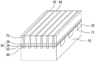
도 1 내지 도 4는 본 발명에 따른 워드라인 더블 패터닝 공정방법에 관한 제 1 실시예를 보여주는 공정 사시도이고, 도 5는 상기 제 1 실시예에 의하여 제조된 낸드 플래시 메모리 어레이의 일 예를 보여준다.1 to 4 are process perspective views showing a first embodiment of a word line double patterning process method according to the present invention, and FIG. 5 shows an example of a NAND flash memory array manufactured according to the first embodiment.
도 6 내지 도 8은 본 발명에 따른 워드라인 더블 패터닝 공정방법에 관한 제 2 실시예를 보여주는 공정 사시도이고, 도 9는 상기 제 2 실시예에 의하여 제조된 낸드 플래시 메모리 어레이의 일 예를 보여준다.6 to 8 are process perspective views showing a second embodiment of a word line double patterning process method according to the present invention, and FIG. 9 shows an example of a NAND flash memory array manufactured according to the second embodiment.
도 10 내지 도 12는 본 발명에 따른 워드라인 더블 패터닝 공정방법에 관한 제 3 실시예를 보여주는 공정 사시도이고, 도 13은 상기 제 3 실시예에 의하여 제조된 낸드 플래시 메모리 어레이의 일 예를 보여준다.10 to 12 are process perspective views showing a third embodiment of a word line double patterning process method according to the present invention, and FIG. 13 shows an example of a NAND flash memory array manufactured according to the third embodiment.
[공정방법 및 이에 의한 낸드 어레이 구조에 관한 제 1 실시예][First Embodiment of Processing Method and NAND Array Structure thereby]
먼저, 워드라인 더블 패터닝 공정방법은, 도 1과 같이, 반도체 기판(10)에 절연막(20)으로 비트라인(12)을 정의한다(제 1 단계).First, in the word line double patterning process method, as shown in FIG. 1, the
여기서, 상기 비트라인(12)을 정의하는 절연막(20) 형성 공정은 공지의 STI 공정이나 필드 산화막 형성 공정에 의할 수 있다.The process of forming the
다음, 도 2와 같이, 상기 비트라인(12)이 정의된 기판 상에 전하저장층이 포함된 2이상의 유전체층(30)을 적층하고(제 2 단계), 이어 상기 유전체층(30) 상에 제 1 전도성 물질을 적층하고 식각하여 제 1 워드라인(40)을 형성한다(제 3 단계).Next, as shown in FIG. 2, two or more
여기서, 상기 전하저장층이 포함된 2이상의 유전체층(30)은 블로킹산화막(36)/질화막(34)/터널링산화막(32)으로 적층된 ONO층이 바람직하다. 이때, 전하저장층은 질화막(34)이 된다. Here, the at least two
물론, 상기 전하저장층(34)으로 질화막 대신 도전성 물질로 대체하여 플로팅게이트 구조로 형성할 수 있음은 물론이다. 그러나, 플로팅게이트 구조로 메모리 셀을 형성할 경우에는 이웃 셀과의 전기적 독립을 위하여 전하저장층으로 사용되는 도전성 물질을 절단시켜주는 별도의 공정을 더 진행하여야 한다.Of course, the
그리고, 상기 제 1 전도성 물질은 도핑된 폴리실리콘이 바람직하다.In addition, the first conductive material is preferably doped polysilicon.
다음, 도 3과 같이, 상기 제 1 워드라인(40) 상에 분리 산화막(50)을 형성한다(제 4 단계). Next, as shown in FIG. 3, a
여기서, 상기 분리 산화막(50) 형성은 열산화 공정에 의하였으나, 공지의 CVD 공정에 의할 수도 있다. 열산화 공정에 의할 경우, 도 3과 같이, 폴리실리콘으 로 이루어진 제 1 워드라인이 잠식되며(42) 분리 산화막(50)이 형성된다. Here, the
상기 분리 산화막(50)은 공정조건을 조절하여 일정 두께로 특히, 2~50 nm의 두께를 갖도록 하는 것이 바람직한데, 이는 별도의 소스/드레인 형성을 위한 이온주입 공정 없이도, 이웃 워드라인의 프린징 필드(fringing field)로 전기적으로 소스/드레인을 형성하는 인버젼 타입의 소스/드레인을 형성하기 위함이다. 즉, 50 nm 이상의 두께를 가지게 되면 결국 이웃 워드라인 간 간격이 넓어져 프린징 필드로 인버젼 타입의 소스/드레인을 형성하기 어렵고, 그렇다고 너무 좁으면 이웃 워드라인 간 전기적 간섭이 커지는 문제점이 있다. 그러나, 상기 분리 산화막(50)의 두께는 워드라인에 가해지는 동작 전압과 워드라인 사이에 채워지는 절연물질의 유전율에 따라 달리 결정될 수 있다.The
이어, 도 4와 같이, 상기 기판 상에 제 2 전도성 물질을 적층하고 식각하여 제 2 워드라인(44)을 형성한다(제 5 단계).Subsequently, as illustrated in FIG. 4, a
여기서, 상기 제 2 전도성 물질은 상기 제 1 전도성 물질과 동일하게 도핑된 폴리실리콘인 것이 바람직하고, 상기 제 2 전도성 물질의 식각은 공지의 CMP 공정 등으로, 도 4와 같이, 상기 제 1 워드라인(42)이 드러나도록 평탄화시키는 것이 바람직하다.Here, the second conductive material is preferably polysilicon doped in the same manner as the first conductive material, the etching of the second conductive material is a known CMP process or the like, as shown in Figure 4, the first word line It is preferable to flatten so that (42) is revealed.
도 4와 같이, 상기 제 2 전도성 물질의 식각으로 기판 상부를 평탄화시켰을 경우, 제 1 워드라인(42)과 제 2 워드라인(44) 사이에는 분리 산화막(52)이 채워진 상태로 남게되고, 상기 제 1 워드라인(42) 및 제 2 워드라인(44)에 일정 전압(VPASS) 이상을 걸어주면 이웃 워드라인의 프린징 필드(fringing field; 62)로 전기적으로 소스/드레인을 형성하는 인버젼 타입의 소스/드레인이 형성되게 되어, 별도의 소스/드레인 형성을 위한 이온주입 공정이 필요 없게 되는 장점이 있다.As shown in FIG. 4, when the upper portion of the substrate is planarized by etching the second conductive material, the
상기와 같은 공정을 통하게 되면, 도 5와 같은 구조를 갖는 낸드 플래시 메모리 어레이를 제조할 수 있다.Through the above process, a NAND flash memory array having a structure as shown in FIG. 5 can be manufactured.
상기 어레이의 특징은 하나의 피치(pitch)에 두개의 워드라인이 형성되어 종래보다 비트 밀도를 1bit/4F2에서 1bit/2F2로 2배 증가시킬 수 있는 장점이 있다.The feature of the array is that two word lines are formed in one pitch, thereby increasing the bit density twice from 1 bit / 4F 2 to 1 bit / 2F 2 than in the prior art.
여기서, Pitch=L1+L2+2Wox=2F (F: minimum feature size) 이고, 프린징 필드(fringing field; 62)로 소스/드레인을 형성하기 위해 상기 제 1 워드라인 및 상기 제 2 워드라인 사이의 간격은 상기 제 1 워드라인 또는 상기 제 2 워드라인의 선폭, 즉 최소선폭(F) 보다 작은 것이 바람직하고, 보다 구체적으로 2~50 nm인 것이 바람직하다.Here, Pitch = L1 + L2 + 2Wox = 2F (F: minimum feature size), and between the first word line and the second word line to form a source / drain with a
그리고, 상기 제 1 워드라인(42)과 상기 제 2 워드라인(44)의 선폭은 상기 제 1 워드라인 및 상기 제 2 워드라인의 간격 만큼 오차 범위내에서 같도록 하여(즉, 제 1, 2 워드라인의 선폭 차이가 이들 간격보다 크지 않도록 하여) 메모리 셀 간의 구동 편차를 줄이는 것이 바람직하다.The line widths of the
[공정방법 및 이에 의한 낸드 어레이 구조에 관한 제 2 실시예][Second embodiment of process method and NAND array structure thereby]
이는 상기 제 1 실시예에서, 도 4와 같이, 상기 제 5 단계의 제 2 전도성 물 질 식각을 상기 제 1 워드라인(42)이 드러나도록 하고, 도 6과 같이, 상기 제 1 워드라인(42) 및 상기 제 2 워드라인(44)을 식각 마스크로 하여 사이에 있는 상기 분리 산화막(52) 및 상기 ONO층(30)의 블로킹산화막(36)/질화막(34)/터널링산화막(32)을 순차 제거하는 제 6 단계와, 도 7과 같이, 상기 분리 산화막(52) 및 상기 블로킹산화막(36)/질화막(34)/터널링산화막(32)의 제거로 드러난 홈을 이용 소스/드레인(60) 형성을 위한 이온주입 공정을 진행하는 제 7 단계와, 도 8과 같이, 상기 홈에 유전율이 높은 절연막을 채우는 제 8 단계 공정을 더 진행한다.In this first embodiment, as shown in FIG. 4, the
상기 제 2 실시예에 의한 공정은 상기 제 4 단계에서 분리 산화막(50)의 두께가 너무 두껍게 형성되거나 워드라인에 가해지는 동작 전압(VPASS)을 낮출 필요가 있을 경우에 유용하게 이용될 수 있고, 이에 의하면, 도 9와 같은 구조를 갖는 낸드 플래시 메모리 어레이를 제조할 수 있다.The process according to the second embodiment may be useful when the thickness of the
상기 제 2 실시예에 의한 어레이의 특징도 하나의 피치(pitch)에 두개의 워드라인이 형성되어 종래보다 비트 밀도를 1bit/4F2에서 1bit/2F2로 2배 증가시킬 수 있는 장점이 있다.The second has the advantage of features also the two word lines are formed in a pitch (pitch) can be increased two times the bit density than the conventional by 1bit / 2F 2 in 1bit / 4F 2 of the array according to the second embodiment.
여기서, Pitch=L1+L2+2Wox=2F (F: minimum feature size) 이고, 상기 제 1 워드라인(42)과 상기 제 2 워드라인(44)의 선폭은 상기 제 1 워드라인 및 상기 제 2 워드라인의 간격 만큼 오차 범위내에서 같도록 하여(즉, 제 1, 2 워드라인의 선폭 차이가 이들 간격보다 크지 않도록 하여) 메모리 셀 간의 구동 편차를 줄이는 것이 바람직하다.Here, Pitch = L1 + L2 + 2Wox = 2F (F: minimum feature size), and the line widths of the
[공정방법 및 이에 의한 낸드 어레이 구조에 관한 제 3 실시예][Third Embodiment Regarding Process Method and NAND Array Structure]
이는, 도 10과 같이, 상기 제 3 단계에서 제 1 워드라인(40)을 형성하기 위해 사용했던 식각 마스크 제거시 상기 블로킹산화막(36)도 선택적으로 제거하여 트렌치(37) 바닥으로 질화막(34)이 드러나도록 한 다음, 도 11과 같이, 상기 제 4 단계의 분리 산화막(38)을 형성하는 것을 특징으로 한다.As shown in FIG. 10, when the etching mask used to form the
여기서, 상기 분리 산화막(38) 형성은 공지의 CVD 공정에 의하였으나, 열산화 공정에 의할 수도 있다. CVD 공정에 의할 경우, 도 11과 같이, 잠식없이 제 1 워드라인(40)을 둘러싸며 트렌치(37) 바닥에도 일정 두께의 분리 산화막(38)을 형성할 수 있다. 이렇게 됨에 따라, 트렌치(37) 폭이 좁아지게 되어 차후 제 2 워드라인의 폭이 상대적으로 작게 되는데, 이를 방지하기 위하여 열산화 공정 및 식각공정을 먼저 진행하여 제 1 워드라인(40)의 폭을 줄인 다음, 상기 CVD 공정으로 분리 산화막(38)을 형성하는 것이 바람직하다.Here, the
상기 분리 산화막(38) 형성 이후에는 상기 제 1 실시예와 동일하게, 도 12와 같이, 상기 기판 상에 제 2 전도성 물질을 적층하고 식각하여 제 2 워드라인(41)을 형성한다. 제 2 워드라인(41)의 하단에는 분리 산화막(38)/질화막(34)/터널링산화막(32)으로 ONO층(31)을 이루게 된다.After the
상기 분리 산화막(38) 형성시 공정조건을 조절하여 일정 두께로 특히, 2~50 nm의 두께를 갖도록 하여 이웃 워드라인의 프린징 필드(fringing field; 62)로 전기적으로 소스/드레인을 형성하는 것도 상기 제 1 실시예와 동일하다.In order to form the source / drain electrically in the
상기 제 3 실시예에 의한 공정을 통하게 되면, 도 13과 같은 구조를 갖는 낸드 플래시 메모리 어레이를 제조할 수 있다.Through the process according to the third embodiment, a NAND flash memory array having a structure as shown in FIG. 13 can be manufactured.
상기 제 3 실시예에 의한 어레이의 특징도 하나의 피치(pitch)에 두개의 워드라인이 형성되어 종래보다 비트 밀도를 1bit/4F2에서 1bit/2F2로 2배 증가시킬 수 있는 장점이 있다.The second has the advantage of features of the array can also have two word lines are formed in a pitch (pitch) increases twice the bit density than the conventional by 1bit / 2F 2 in 1bit / 4F 2 according to the third embodiment.
여기서, Pitch=L3+L4+2Wox=2F (F: minimum feature size) 이고, 프린징 필드(fringing field; 62)로 소스/드레인을 형성하기 위해 상기 제 1 워드라인 및 상기 제 2 워드라인 사이의 간격은 상기 제 1 워드라인 또는 상기 제 2 워드라인의 선폭, 즉 최소선폭(F) 보다 작은 것이 바람직하고, 보다 구체적으로 2~50 nm인 것이 바람직하다.Here, Pitch = L3 + L4 + 2Wox = 2F (F: minimum feature size), and between the first word line and the second word line to form a source / drain with a
그리고, 상기 제 1 워드라인(40)과 상기 제 2 워드라인(41)의 선폭은 상기 제 1 워드라인 및 상기 제 2 워드라인의 간격 만큼 오차 범위내에서 같도록 하여(즉, 제 1, 2 워드라인의 선폭 차이가 이들 간격보다 크지 않도록 하여) 메모리 셀 간의 구동 편차를 줄이는 것이 바람직하다.The line widths of the
이상으로 본 발명의 바람직한 실시예에 대하여 기술하였으나, 하기 특허청구범위에 기재된 기술적 사상은 상기 실시예에 국한되지 아니하고, 상기 실시예를 토대로 다양하게 균등물의 대체 등으로 실시될 수 있는바, 이에 대한 설명은 생략한다.Although the preferred embodiments of the present invention have been described above, the technical idea described in the following claims is not limited to the above embodiments, and can be carried out by replacing various equivalents based on the embodiments. Description is omitted.
도 1 내지 도 4는 본 발명에 따른 워드라인 더블 패터닝 공정방법에 관한 제 1 실시예를 보여주는 공정 사시도이다. 1 to 4 are process perspective views showing a first embodiment of a word line double patterning process method according to the present invention.
도 5는 상기 제 1 실시예에 의하여 제조된 낸드 플래시 메모리 어레이의 일 예를 보여주는 구조 사시도이다.FIG. 5 is a structural perspective view illustrating an example of a NAND flash memory array manufactured according to the first embodiment.
도 6 내지 도 8은 본 발명에 따른 워드라인 더블 패터닝 공정방법에 관한 제 2 실시예를 보여주는 공정 사시도이다.6 to 8 are process perspective views showing a second embodiment of a word line double patterning process method according to the present invention.
도 9는 상기 제 2 실시예에 의하여 제조된 낸드 플래시 메모리 어레이의 일 예를 보여주는 구조 사시도이다.9 is a structural perspective view showing an example of a NAND flash memory array manufactured by the second embodiment.
도 10 내지 도 12는 본 발명에 따른 워드라인 더블 패터닝 공정방법에 관한 제 3 실시예를 보여주는 공정 사시도이다.10 to 12 are process perspective views showing a third embodiment of a word line double patterning process method according to the present invention.
도 13은 상기 제 3 실시예에 의하여 제조된 낸드 플래시 메모리 어레이의 일 예를 보여주는 구조 사시도이다.FIG. 13 is a structural perspective view illustrating an example of a NAND flash memory array manufactured according to the third embodiment.
<도면의 주요부분에 대한 부호의 설명><Description of the symbols for the main parts of the drawings>
10: 반도체 기판 12: 비트라인10: semiconductor substrate 12: bit line
20: 절연막 30, 31: ONO층20: insulating
40, 42: 제 1 워드라인 44: 제 2 워드라인40, 42: first word line 44: second word line
50: 분리 산화막 60: 소스/드레인50: separation oxide film 60: source / drain
Claims (8)
Priority Applications (1)
| Application Number | Priority Date | Filing Date | Title |
|---|---|---|---|
| KR1020090030181A KR20100111798A (en) | 2009-04-08 | 2009-04-08 | Method for word line double patterning process and nand flash memory array fabricated by the same |
Applications Claiming Priority (1)
| Application Number | Priority Date | Filing Date | Title |
|---|---|---|---|
| KR1020090030181A KR20100111798A (en) | 2009-04-08 | 2009-04-08 | Method for word line double patterning process and nand flash memory array fabricated by the same |
Publications (1)
| Publication Number | Publication Date |
|---|---|
| KR20100111798A true KR20100111798A (en) | 2010-10-18 |
Family
ID=43131907
Family Applications (1)
| Application Number | Title | Priority Date | Filing Date |
|---|---|---|---|
| KR1020090030181A Ceased KR20100111798A (en) | 2009-04-08 | 2009-04-08 | Method for word line double patterning process and nand flash memory array fabricated by the same |
Country Status (1)
| Country | Link |
|---|---|
| KR (1) | KR20100111798A (en) |
Cited By (6)
| Publication number | Priority date | Publication date | Assignee | Title |
|---|---|---|---|---|
| US8389353B2 (en) | 2010-03-09 | 2013-03-05 | Micron Technology, Inc. | Methods of forming an array of memory cells, methods of forming a plurality of field effect transistors, methods of forming source/drain regions and isolation trenches, and methods of forming a series of spaced trenches into a substrate |
| US8791443B2 (en) | 2012-05-24 | 2014-07-29 | SK Hynix Inc. | High density variable resistive memory and method of fabricating the same |
| US9005463B2 (en) | 2013-05-29 | 2015-04-14 | Micron Technology, Inc. | Methods of forming a substrate opening |
| US9153705B2 (en) | 2013-02-26 | 2015-10-06 | Samsung Electronics Co., Ltd. | Vertical memory devices and methods of manufacturing the same |
| US9236417B2 (en) | 2012-08-23 | 2016-01-12 | SK Hynix Inc. | 3-dimensional stack memory device |
| US9385132B2 (en) | 2011-08-25 | 2016-07-05 | Micron Technology, Inc. | Arrays of recessed access devices, methods of forming recessed access gate constructions, and methods of forming isolation gate constructions in the fabrication of recessed access devices |
-
2009
- 2009-04-08 KR KR1020090030181A patent/KR20100111798A/en not_active Ceased
Cited By (9)
| Publication number | Priority date | Publication date | Assignee | Title |
|---|---|---|---|---|
| US8389353B2 (en) | 2010-03-09 | 2013-03-05 | Micron Technology, Inc. | Methods of forming an array of memory cells, methods of forming a plurality of field effect transistors, methods of forming source/drain regions and isolation trenches, and methods of forming a series of spaced trenches into a substrate |
| US8586429B2 (en) | 2010-03-09 | 2013-11-19 | Micron Technology, Inc. | Methods of forming an array of memory cells, methods of forming a plurality of field effect transistors, methods of forming source/drain regions and isolation trenches, and methods of forming a series of spaced trenches into a substrate |
| US8796086B2 (en) | 2010-03-09 | 2014-08-05 | Micron Technology, Inc. | Methods of forming an array of memory cells, methods of forming a plurality of field effect transistors, methods of forming source/drain regions and isolation trenches, and methods of forming a series of spaced trenches into a substrate |
| US9385132B2 (en) | 2011-08-25 | 2016-07-05 | Micron Technology, Inc. | Arrays of recessed access devices, methods of forming recessed access gate constructions, and methods of forming isolation gate constructions in the fabrication of recessed access devices |
| US8791443B2 (en) | 2012-05-24 | 2014-07-29 | SK Hynix Inc. | High density variable resistive memory and method of fabricating the same |
| US9236417B2 (en) | 2012-08-23 | 2016-01-12 | SK Hynix Inc. | 3-dimensional stack memory device |
| US9153705B2 (en) | 2013-02-26 | 2015-10-06 | Samsung Electronics Co., Ltd. | Vertical memory devices and methods of manufacturing the same |
| US9005463B2 (en) | 2013-05-29 | 2015-04-14 | Micron Technology, Inc. | Methods of forming a substrate opening |
| US9443756B2 (en) | 2013-05-29 | 2016-09-13 | Micron Technology, Inc. | Methods of forming a substrate opening |
Similar Documents
| Publication | Publication Date | Title |
|---|---|---|
| US11069410B1 (en) | Three-dimensional NOR-NAND combination memory device and method of making the same | |
| JP6339672B2 (en) | Method and apparatus having a memory cell string including a metal source | |
| US7589374B2 (en) | Semiconductor device and related fabrication method | |
| US11127862B2 (en) | Three-dimensional non-volatile memory device and method of manufacturing the same | |
| KR20170036878A (en) | Three dimensional semiconductor device | |
| CN102237368A (en) | Nonvolatile memory device and method for fabricating the same | |
| CN106024794A (en) | Semiconductor device and manufacturing method thereof | |
| CN110289265B (en) | Method for forming 3D NAND memory | |
| CN103579125A (en) | Nonvolatile memory device and method for fabricating the same | |
| JP5361335B2 (en) | Nonvolatile semiconductor memory device and manufacturing method thereof | |
| KR20100111798A (en) | Method for word line double patterning process and nand flash memory array fabricated by the same | |
| US11664281B2 (en) | Semiconductor device | |
| US20160233221A1 (en) | Flash memory semiconductor device | |
| KR100620223B1 (en) | Manufacturing method of split gate flash Y pyrom | |
| CN106206446A (en) | Embed the manufacture method of the flash memory of logic circuit | |
| JP4250616B2 (en) | Semiconductor integrated circuit device and manufacturing method thereof | |
| JP2011066052A (en) | Semiconductor device manufacturing method, and the semiconductor device | |
| US20120025293A1 (en) | Semiconductor memory device having a floating gate and a control gate and method of manufacturing the same | |
| EP1782460B1 (en) | Method for fabricating a floating gate memory cell | |
| US20100314677A1 (en) | Semiconductor storage device and method of manufacturing the same | |
| KR100673011B1 (en) | NOR flash memory device and manufacturing method thereof | |
| TWI908024B (en) | Sonos memory device and manufacturing method of the same | |
| KR20100120787A (en) | Nand flash memory array with extended charge storage node and fabrication method of the same | |
| TWI423398B (en) | Memory cell and its manufacturing method and memory structure | |
| JP3141934B2 (en) | Manufacturing method of nonvolatile semiconductor memory device |
Legal Events
| Date | Code | Title | Description |
|---|---|---|---|
| A201 | Request for examination | ||
| PA0109 | Patent application |
St.27 status event code: A-0-1-A10-A12-nap-PA0109 |
|
| PA0201 | Request for examination |
St.27 status event code: A-1-2-D10-D11-exm-PA0201 |
|
| PG1501 | Laying open of application |
St.27 status event code: A-1-1-Q10-Q12-nap-PG1501 |
|
| D13-X000 | Search requested |
St.27 status event code: A-1-2-D10-D13-srh-X000 |
|
| D14-X000 | Search report completed |
St.27 status event code: A-1-2-D10-D14-srh-X000 |
|
| E902 | Notification of reason for refusal | ||
| PE0902 | Notice of grounds for rejection |
St.27 status event code: A-1-2-D10-D21-exm-PE0902 |
|
| T11-X000 | Administrative time limit extension requested |
St.27 status event code: U-3-3-T10-T11-oth-X000 |
|
| E13-X000 | Pre-grant limitation requested |
St.27 status event code: A-2-3-E10-E13-lim-X000 |
|
| P11-X000 | Amendment of application requested |
St.27 status event code: A-2-2-P10-P11-nap-X000 |
|
| P13-X000 | Application amended |
St.27 status event code: A-2-2-P10-P13-nap-X000 |
|
| PN2301 | Change of applicant |
St.27 status event code: A-3-3-R10-R13-asn-PN2301 St.27 status event code: A-3-3-R10-R11-asn-PN2301 |
|
| E601 | Decision to refuse application | ||
| PE0601 | Decision on rejection of patent |
St.27 status event code: N-2-6-B10-B15-exm-PE0601 |
|
| R18-X000 | Changes to party contact information recorded |
St.27 status event code: A-3-3-R10-R18-oth-X000 |
|
| PN2301 | Change of applicant |
St.27 status event code: A-3-3-R10-R13-asn-PN2301 St.27 status event code: A-3-3-R10-R11-asn-PN2301 |
|
| PN2301 | Change of applicant |
St.27 status event code: A-3-3-R10-R13-asn-PN2301 St.27 status event code: A-3-3-R10-R11-asn-PN2301 |
|
| P22-X000 | Classification modified |
St.27 status event code: A-2-2-P10-P22-nap-X000 |
|
| R18-X000 | Changes to party contact information recorded |
St.27 status event code: A-3-3-R10-R18-oth-X000 |
|
| R18-X000 | Changes to party contact information recorded |
St.27 status event code: A-3-3-R10-R18-oth-X000 |
|
| PN2301 | Change of applicant |
St.27 status event code: A-3-3-R10-R13-asn-PN2301 St.27 status event code: A-3-3-R10-R11-asn-PN2301 |
|
| PN2301 | Change of applicant |
St.27 status event code: A-3-3-R10-R13-asn-PN2301 St.27 status event code: A-3-3-R10-R11-asn-PN2301 |
|
| R18-X000 | Changes to party contact information recorded |
St.27 status event code: A-3-3-R10-R18-oth-X000 |
|
| R18-X000 | Changes to party contact information recorded |
St.27 status event code: A-3-3-R10-R18-oth-X000 |
|
| R18-X000 | Changes to party contact information recorded |
St.27 status event code: A-3-3-R10-R18-oth-X000 |
|
| R18-X000 | Changes to party contact information recorded |
St.27 status event code: A-3-3-R10-R18-oth-X000 |
|
| P22-X000 | Classification modified |
St.27 status event code: A-2-2-P10-P22-nap-X000 |
|
| R18-X000 | Changes to party contact information recorded |
St.27 status event code: A-3-3-R10-R18-oth-X000 |
|
| R18-X000 | Changes to party contact information recorded |
St.27 status event code: A-3-3-R10-R18-oth-X000 |
|
| R18 | Changes to party contact information recorded |
Free format text: ST27 STATUS EVENT CODE: A-3-3-R10-R18-OTH-X000 (AS PROVIDED BY THE NATIONAL OFFICE) |
|
| R18-X000 | Changes to party contact information recorded |
St.27 status event code: A-3-3-R10-R18-oth-X000 |
|
| P22-X000 | Classification modified |
St.27 status event code: A-2-2-P10-P22-nap-X000 |