KR20100049027A - Infrared and dual mode displays - Google Patents
Infrared and dual mode displays Download PDFInfo
- Publication number
- KR20100049027A KR20100049027A KR1020107000995A KR20107000995A KR20100049027A KR 20100049027 A KR20100049027 A KR 20100049027A KR 1020107000995 A KR1020107000995 A KR 1020107000995A KR 20107000995 A KR20107000995 A KR 20107000995A KR 20100049027 A KR20100049027 A KR 20100049027A
- Authority
- KR
- South Korea
- Prior art keywords
- display device
- light
- infrared light
- display
- wavelength
- Prior art date
- Legal status (The legal status is an assumption and is not a legal conclusion. Google has not performed a legal analysis and makes no representation as to the accuracy of the status listed.)
- Ceased
Links
Images


Classifications
-
- G—PHYSICS
- G02—OPTICS
- G02B—OPTICAL ELEMENTS, SYSTEMS OR APPARATUS
- G02B26/00—Optical devices or arrangements for the control of light using movable or deformable optical elements
- G02B26/001—Optical devices or arrangements for the control of light using movable or deformable optical elements based on interference in an adjustable optical cavity
-
- G—PHYSICS
- G02—OPTICS
- G02B—OPTICAL ELEMENTS, SYSTEMS OR APPARATUS
- G02B26/00—Optical devices or arrangements for the control of light using movable or deformable optical elements
- G02B26/08—Optical devices or arrangements for the control of light using movable or deformable optical elements for controlling the direction of light
- G02B26/0816—Optical devices or arrangements for the control of light using movable or deformable optical elements for controlling the direction of light by means of one or more reflecting elements
- G02B26/0833—Optical devices or arrangements for the control of light using movable or deformable optical elements for controlling the direction of light by means of one or more reflecting elements the reflecting element being a micromechanical device, e.g. a MEMS mirror, DMD
-
- G—PHYSICS
- G02—OPTICS
- G02B—OPTICAL ELEMENTS, SYSTEMS OR APPARATUS
- G02B5/00—Optical elements other than lenses
- G02B5/20—Filters
- G02B5/208—Filters for use with infrared or ultraviolet radiation, e.g. for separating visible light from infrared and/or ultraviolet radiation
-
- G—PHYSICS
- G09—EDUCATION; CRYPTOGRAPHY; DISPLAY; ADVERTISING; SEALS
- G09G—ARRANGEMENTS OR CIRCUITS FOR CONTROL OF INDICATING DEVICES USING STATIC MEANS TO PRESENT VARIABLE INFORMATION
- G09G3/00—Control arrangements or circuits, of interest only in connection with visual indicators other than cathode-ray tubes
- G09G3/20—Control arrangements or circuits, of interest only in connection with visual indicators other than cathode-ray tubes for presentation of an assembly of a number of characters, e.g. a page, by composing the assembly by combination of individual elements arranged in a matrix no fixed position being assigned to or needed to be assigned to the individual characters or partial characters
- G09G3/34—Control arrangements or circuits, of interest only in connection with visual indicators other than cathode-ray tubes for presentation of an assembly of a number of characters, e.g. a page, by composing the assembly by combination of individual elements arranged in a matrix no fixed position being assigned to or needed to be assigned to the individual characters or partial characters by control of light from an independent source
- G09G3/3433—Control arrangements or circuits, of interest only in connection with visual indicators other than cathode-ray tubes for presentation of an assembly of a number of characters, e.g. a page, by composing the assembly by combination of individual elements arranged in a matrix no fixed position being assigned to or needed to be assigned to the individual characters or partial characters by control of light from an independent source using light modulating elements actuated by an electric field and being other than liquid crystal devices and electrochromic devices
- G09G3/3466—Control arrangements or circuits, of interest only in connection with visual indicators other than cathode-ray tubes for presentation of an assembly of a number of characters, e.g. a page, by composing the assembly by combination of individual elements arranged in a matrix no fixed position being assigned to or needed to be assigned to the individual characters or partial characters by control of light from an independent source using light modulating elements actuated by an electric field and being other than liquid crystal devices and electrochromic devices based on interferometric effect
-
- G—PHYSICS
- G09—EDUCATION; CRYPTOGRAPHY; DISPLAY; ADVERTISING; SEALS
- G09G—ARRANGEMENTS OR CIRCUITS FOR CONTROL OF INDICATING DEVICES USING STATIC MEANS TO PRESENT VARIABLE INFORMATION
- G09G2320/00—Control of display operating conditions
- G09G2320/06—Adjustment of display parameters
- G09G2320/0666—Adjustment of display parameters for control of colour parameters, e.g. colour temperature
-
- H—ELECTRICITY
- H04—ELECTRIC COMMUNICATION TECHNIQUE
- H04N—PICTORIAL COMMUNICATION, e.g. TELEVISION
- H04N5/00—Details of television systems
- H04N5/74—Projection arrangements for image reproduction, e.g. using eidophor
- H04N5/7416—Projection arrangements for image reproduction, e.g. using eidophor involving the use of a spatial light modulator, e.g. a light valve, controlled by a video signal
- H04N5/7458—Projection arrangements for image reproduction, e.g. using eidophor involving the use of a spatial light modulator, e.g. a light valve, controlled by a video signal the modulator being an array of deformable mirrors, e.g. digital micromirror device [DMD]
- H04N2005/7466—Control circuits therefor
Landscapes
- Physics & Mathematics (AREA)
- General Physics & Mathematics (AREA)
- Optics & Photonics (AREA)
- Engineering & Computer Science (AREA)
- Computer Hardware Design (AREA)
- Toxicology (AREA)
- Health & Medical Sciences (AREA)
- Theoretical Computer Science (AREA)
- Spectroscopy & Molecular Physics (AREA)
- Mechanical Light Control Or Optical Switches (AREA)
- Devices For Indicating Variable Information By Combining Individual Elements (AREA)
- Micromachines (AREA)
- Control Of Indicators Other Than Cathode Ray Tubes (AREA)
Abstract
본 발명의 일 양상은 적외광 영역의 제1 파장의 광과 가시광 영역의 제2 파장의 광을 선택적으로 반사시키도록 구성된 표시소자(102)를 포함하는 표시장치(100)에 관한 것이다. 본 발명의 다른 양상은 적어도 3개의 반사형 표시소자(104, 106, 108)를 포함하는 컬러 표시장치(100)에 관한 것이다. 각 표시소자(104, 106, 108)는 가시광 영역에서의 상이한 파장의 광을 선택적으로 반사시키도록 구성되어 있다. 3개의 반사형 표시소자(104, 106, 108) 중 적어도 하나는 적외광 영역의 파장의 광을 선택적으로 반사시키도록 구성되어 있다.One aspect of the present invention relates to a display device 100 including a display element 102 configured to selectively reflect light of a first wavelength in an infrared light region and light of a second wavelength in a visible light region. Another aspect of the invention relates to a color display device 100 comprising at least three reflective display elements 104, 106, 108. Each display element 104, 106, 108 is configured to selectively reflect light of different wavelengths in the visible light region. At least one of the three reflective display elements 104, 106 and 108 is configured to selectively reflect light of the wavelength of the infrared light region.
Description
본 발명의 기술분야는 MEMS(microelectromechanical systems: 마이크로전자기계 시스템)에 관한 것이다.TECHNICAL FIELD The present invention relates to microelectromechanical systems (MEMS).
마이크로전자기계 시스템(MEMS)은 마이크로기계 소자, 작동기 및 전자 기기를 포함한다. 마이크로기계 소자는 기판 및/또는 증착(혹은 침착(deposition); 이하 본 명세서에서는 "증착"이라 표기함)된 재료층의 일부를 에칭해내거나 층들을 추가하여 전기 및 전자기계 장치를 형성하는 증착, 에칭 및/또는 기타 미세기계가공(micromachining) 공정들을 이용하여 형성될 수도 있다. MEMS 장치의 한 유형은 간섭계 변조기라 불린다. 본 명세서에서 이용되는 바와 같이, 간섭계 변조기(interferometric modulator) 또는 간섭계 광 변조기(interferometric light modulator)라는 용어는 광학적 간섭의 원리를 이용하여 광을 선택적으로 흡수 및/또는 반사하는 장치를 의미한다. 소정의 실시형태에 있어서, 간섭계 변조기는 1쌍의 도전판을 포함할 수도 있는 데, 상기 1쌍의 도전판의 어느 하나 또는 양쪽 모두가 전체 또는 부분적으로 투과형 및/또는 반사형일 수도 있고 적절한 전기 신호의 인가시 상대 운동을 할 수 있다. 특별한 실시형태에 있어서, 하나의 도전판은 기판에 증착된 고정층을 포함할 수도 있고, 다른 하나의 도전판은 공기 간극(air gap)에 의해 고정층과는 분리된 금속막을 포함할 수도 있다. 본 명세서에서 보다 더 상세히 설명하는 바와 같이, 도전판의 상대적 위치에 의해서 간섭계 변조기에 입사되는 광의 광학적 간섭은 변화될 수 있다. 이러한 장치들의 적용 범위는 광범위하며, 기존의 제품들을 개선시키는 데 있어서, 그리고 아직 개발되지 않은 새로운 제품들을 만들어내는 데 있어서 이러한 유형의 장치 특성들이 사용될 수 있도록 이들 장치의 특징들을 이용 및/또는 변경하는 것은 해당 기술 분야에서 유용할 것이다.Microelectromechanical systems (MEMS) include micromechanical elements, actuators and electronic devices. A micromechanical element may be a substrate and / or deposition that deposits a portion of a deposited (or deposited; hereafter referred to as "deposition") or adds layers to form an electromechanical device, It may be formed using etching and / or other micromachining processes. One type of MEMS device is called an interferometric modulator. As used herein, the term interferometric modulator or interferometric light modulator means an apparatus that selectively absorbs and / or reflects light using the principles of optical interference. In certain embodiments, the interferometric modulator may comprise a pair of conductive plates, wherein either or both of the pair of conductive plates may be transmissive and / or reflective in whole or in part and suitable electrical signals. You can do relative exercise when In a particular embodiment, one conductive plate may comprise a pinned layer deposited on a substrate, and the other conductive plate may comprise a metal film separated from the fixed layer by an air gap. As will be explained in more detail herein, the optical interference of light incident on the interferometric modulator can be varied by the relative position of the conductive plate. The range of applications of these devices is broad, and the use and / or modification of the features of these devices can be used to improve existing products and to create new products that have not yet been developed. Will be useful in the art.
본 명세서에 개시된 시스템, 방법 및 장치는 각각 수개의 양상들을 지니고 있으며, 이들 각각의 어느 하나만이 단독으로 그것의 목적으로 하는 속성을 담당하지는 않는다. 본 발명의 범위를 한정하는 일없이, 본 발명의 더욱 뛰어난 특징들이 지금부터 간단하게 논의될 것이다. 당업자는, 이 논의를 고려한 후에, 그리고 특히 "실시예" 부분을 읽은 후에, 본 발명의 특징들이 어떻게 다른 표시장치에 비해 장점을 제공하는지 이해할 수 있을 것이다.The systems, methods, and apparatus disclosed herein each have several aspects, and not each of these alone is responsible for its intended attributes. Without limiting the scope of the invention, further superior features of the invention will now be discussed briefly. Those skilled in the art will understand how the features of the present invention provide advantages over other displays, after considering this discussion, and in particular after reading the "embodiments" section.
본 발명은 특정 구성의 표시장치, 특히 컬러 표시장치, 및 이러한 표시장치의 작동방법을 제공하는 데 있다.The present invention provides a display device having a specific configuration, in particular a color display device, and a method of operating such a display device.
일 양상에 있어서, 디스플레이, 즉, 표시장치가 개시되어 있다. 해당 표시장치는 적외광 영역의 제1 파장의 광과 가시광 영역의 제2 파장의 광을 선택적으로 반사시키도록 구성된 표시 소자를 포함한다.In one aspect, a display, i.e. a display, is disclosed. The display device includes a display element configured to selectively reflect light at a first wavelength in an infrared light region and light at a second wavelength in a visible light region.
다른 양상에 있어서, 컬러 표시장치가 개시되어 있다. 해당 표시장치는 적어도 3개의 반사형 표시소자를 포함한다. 각 표시소자는 가시광 영역에서의 상이한 파장의 광을 선택적으로 반사시키도록 구성되어 있다. 3개의 반사형 표시소자 중 적어도 1개는 적외광 영역의 파장의 광을 선택적으로 반사시키도록 추가로 구성되어 있다.In another aspect, a color display device is disclosed. The display device includes at least three reflective display elements. Each display element is configured to selectively reflect light of a different wavelength in the visible light region. At least one of the three reflective display elements is further configured to selectively reflect light of the wavelength of the infrared light region.
또 다른 양상에 있어서, 표시장치가 개시되어 있다. 해당 표시장치는 가시광 영역의 파장의 광과 적외광 영역의 파장의 광을 선택적으로 반사시키는 반사수단을 포함한다. 상기 표시장치는 상기 반사수단에 적어도 하나의 신호를 전송하는 전송수단을 추가로 포함한다.In another aspect, a display device is disclosed. The display device includes reflecting means for selectively reflecting light of the wavelength of the visible region and light of the wavelength of the infrared region. The display device further includes transmission means for transmitting at least one signal to the reflecting means.
다른 양상에 있어서, 표시장치를 작동시키는 방법이 개시되어 있다. 해당 방법은 상기 표시장치를 가시광 모드로부터 적외광 모드로 전환시키는 단계를 포함한다. 상기 방법은 상기 적외광 모드와 연관된 방식(scheme)으로 상기 표시장치를 구동시키는 단계를 추가로 포함한다.In another aspect, a method of operating a display device is disclosed. The method includes switching the display device from visible light mode to infrared light mode. The method further includes driving the display device in a scheme associated with the infrared light mode.
또 다른 양상에 있어서, 표시장치를 제조하는 방법이 개시되어 있다. 해당 방법은 적외광 영역의 제1 파장의 광과 가시광 영역의 제2 파장의 광을 선택적으로 반사시키도록 구성된 표시소자를 제조하는 단계를 포함한다.In another aspect, a method of manufacturing a display device is disclosed. The method includes manufacturing a display element configured to selectively reflect light of a first wavelength in an infrared light region and light of a second wavelength in a visible light region.
다른 양상에 있어서, 표시장치가 개시되어 있다. 해당 표시장치는 제1 영역의 파장의 광과 제2 영역의 파장의 광을 선택적으로 반사시키도록 구성된 제1 표시소자를 포함하되, 상기 제1 및 제2 영역의 각각은 자외광 스펙트럼, 가시광 스펙트럼 혹은 적외광 스펙트럼 중 하나 이내이다.In another aspect, a display device is disclosed. The display device includes a first display element configured to selectively reflect light of a wavelength of a first region and light of a wavelength of a second region, wherein each of the first and second regions has an ultraviolet light spectrum and a visible light spectrum. Or within one of the infrared spectrums.
도 1은 제1간섭계 변조기의 이동식 반사층이 이완 위치에 있고, 제2간섭계 변조기의 이동식 반사층이 작동 위치에 있는 간섭계 변조기 디스플레이(표시장치)의 일 실시형태의 일부를 나타낸 등각 투상도;
도 2는 3×3 간섭계 변조기 디스플레이를 내장하는 전자 장치의 일 실시형태를 예시한 시스템 블록도;
도 3은 도 1의 간섭계 변조기의 예시적인 일 실시형태에 대해 이동식 미러(movable mirror)의 위치 대 인가된 전압을 나타낸 선도;
도 4는 간섭계 변조기 디스플레이를 구동하는 데 사용될 수 있는 한 세트의 행방향 전압(row voltage) 및 열방향 전압(column voltage)을 나타낸 도면;
도 5a는 도 2의 3×3 간섭계 변조기 디스플레이에 있어서의 표시 데이터의 하나의 예시적인 프레임을 예시한 도면;
도 5b는 도 5a의 프레임을 기록하는(write) 데 이용될 수 있는 행방향 신호 및 열방향 신호의 하나의 예시적인 타이밍 선도를 나타낸 도면;
도 6a 및 도 6b는 복수개의 간섭계 변조기를 포함하는 비쥬얼 표시장치(visual display device)의 일 실시형태를 나타낸 시스템 블록도;
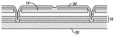
도 7a는 도 1의 장치의 단면도;
도 7b는 간섭계 변조기의 대안적인 실시형태의 단면도;
도 7c는 간섭계 변조기의 다른 대안적인 실시형태의 단면도;
도 7d는 간섭계 변조기의 또 다른 대안적인 실시형태의 단면도;
도 7e는 간섭계 변조기의 추가의 대안적인 실시형태의 단면도;
도 8은 가시광 스펙트럼과 IR(적외광) 스펙트럼의 양쪽 모두에서 볼 수 있는 이색 표시장치(bi-chrome display)(100)의 일 실시형태를 나타낸 도면;
도 9는 약 480 ㎚의 명 상태(bright state) 광학적 간극 길이를 지닌 예시적인 간섭계 변조기의 분광 응답을 나타낸 도면;
도 10은 다른 예시적인 간섭계 변조기의 분광 응답을 나타낸 도면;
도 11은 가시광 스펙트럼과 IR 스펙트럼의 양쪽 모두에서 볼 수 있는 컬러 표시장치(100)의 일 실시형태를 나타낸 도면;
도 12는 본 명세서에 기재된 표시장치에서 적외광 화상(혹은 영상 혹은 이미지)을 표시하는 방법의 일 실시형태를 나타낸 순서도;
도 13은 표시장치를 IR 스펙트럼 모드와 가시광 스펙트럼 모드 간에 작동시키는 방법의 일 실시형태를 나타낸 순서도.1 is an isometric view of a portion of one embodiment of an interferometric modulator display (display) with the movable reflective layer of the first interferometric modulator in a relaxed position and the movable reflective layer of the second interferometric modulator in an operating position;
2 is a system block diagram illustrating one embodiment of an electronic device incorporating a 3x3 interferometric modulator display.
3 is a diagram showing the position of the movable mirror versus the applied voltage for one exemplary embodiment of the interferometric modulator of FIG. 1;
4 shows a set of row and column voltages that can be used to drive an interferometric modulator display;
5A illustrates one exemplary frame of display data in the 3x3 interferometric modulator display of FIG.
FIG. 5B illustrates one exemplary timing diagram of the row and column signals that may be used to write the frame of FIG. 5A; FIG.
6A and 6B are system block diagrams illustrating one embodiment of a visual display device including a plurality of interferometric modulators.
7A is a cross-sectional view of the device of FIG. 1;
7B is a cross-sectional view of an alternative embodiment of an interferometric modulator;
7C is a cross-sectional view of another alternative embodiment of an interferometric modulator;
7D is a cross-sectional view of another alternative embodiment of an interferometric modulator;
7E is a sectional view of a further alternative embodiment of an interferometric modulator;
FIG. 8 shows an embodiment of a
9 shows the spectral response of an exemplary interferometric modulator having a bright state optical gap length of about 480 nm;
10 shows the spectral response of another exemplary interferometric modulator;
FIG. 11 shows an embodiment of a
12 is a flow chart showing one embodiment of a method for displaying an infrared light image (or image or image) in the display device described herein;
13 is a flow diagram illustrating one embodiment of a method of operating a display device between an IR spectral mode and a visible light spectral mode.
이하의 상세한 설명은 본 발명의 임의의 특정 실시형태들에 관한 것이지만, 본 발명은 다양한 방법들로 구현될 수 있다. 본 설명에 있어서, 도면 전체에 걸쳐서 동일한 구성 요소들은 동일한 참조 번호들로 표기된 도면을 참조한다. 이하의 설명으로부터 명백한 바와 같이, 각 실시형태는 동화상(예를 들어, 비디오)인지 또는 정지화상(예를 들어, 스틸 이미지(still image))인지, 그리고 문자인지 그림인지의 여부에 따라 화상을 표시하도록 구성되는 장치이면 어떠한 장치에서도 구현될 수도 있다. 더욱 상세하게는, 휴대폰, 무선 장치, PDA(personal data assistant), 초소형 또는 휴대용 컴퓨터, GPS 수신기/네비게이션, 카메라, MP3 플레이어, 캠코더, 게임 콘솔(game console), 손목 시계, 시계, 계산기, 텔레비전 모니터, 플랫 패널 디스플레이, 컴퓨터 모니터, 자동차 디스플레이(예를 들어, 주행 기록계 디스플레이 등), 콕핏 제어기(cockpit control) 및/또는 디스플레이, 카메라 뷰 디스플레이(예를 들어, 차량의 리어 뷰(rear view) 카메라의 디스플레이), 전자 사진, 전자 광고판 또는 간판, 프로젝터, 건축 구조물, 포장물 및 미술 구조물(예를 들어, 보석류에 대한 화상의 디스플레이)을 포함하지만 이들로 한정되지는 않는 다양한 전자 장치들로 구현되거나 또는 그 다양한 전자 장치들과 관련될 수 있는 것을 고려할 수 있다. 본 명세서에 기재된 것과 마찬가지의 구조체의 MEMS 장치는 또한 전자 전환 장치 등에서와 같은 표시장치가 아닌 용도에도 이용될 수 있다.Although the following detailed description relates to any particular embodiment of the present invention, the present invention may be implemented in various ways. In the present description, the same components refer to the drawings denoted by the same reference numerals throughout the drawings. As will be apparent from the description below, each embodiment displays an image according to whether it is a moving image (e.g. video) or a still image (e.g. still image), and whether it is a character or a picture. Any device may be implemented as long as the device is configured to do so. More specifically, mobile phones, wireless devices, personal data assistants (PDAs), micro or portable computers, GPS receivers / navigations, cameras, MP3 players, camcorders, game consoles, wrist watches, watches, calculators, television monitors Flat panel displays, computer monitors, automotive displays (e.g., odometer displays, etc.), cockpit controls and / or displays, camera view displays (e.g., rear view cameras of vehicles) Display), electronic photographs, electronic billboards or signs, projectors, architectural structures, packages and art structures (e.g., display of images for jewelry), or implemented in various electronic devices, including but not limited to It is contemplated that this may be associated with various electronic devices. MEMS devices of structures similar to those described herein can also be used for applications other than display devices such as in electronic switching devices and the like.
소정의 실시형태는 가시광 스펙트럼과 적외광 스펙트럼의 양쪽 모두에서 반사성인 표시장치를 제공한다. 해당 표시장치는 하나 이상의 간섭계 변조기를 포함할 수 있다. 일 실시형태에 있어서, 상기 표시장치는 가시광 모드와 적외광(IR) 모드의 두 가지 모드에서 이용가능하다. 상기 표시장치는 이들 두 가지 모드 간에 전환하는 기구를 추가로 포함할 수 있다. 도 1 내지 도 7은 간섭계 디스플레이(즉, 표시장치)를 예시하고, 도 8 내지 도 13은 가시광 스펙트럼과 IR 스펙트럼의 양쪽 모두에서 반사성인 간섭계 디스플레이를 예시하고 있다.Certain embodiments provide a display device that is reflective in both the visible spectrum and the infrared spectrum. The display device may include one or more interferometric modulators. In one embodiment, the display device is available in two modes, visible light mode and infrared light (IR) mode. The display device may further comprise a mechanism for switching between these two modes. 1 through 7 illustrate an interferometer display (ie, a display), and FIGS. 8 through 13 illustrate an interferometer display that is reflective in both the visible light spectrum and the IR spectrum.
간섭계 MEMS 표시 소자를 포함하는 간섭계 변조기 디스플레이의 일 실시형태가 도 1에 예시되어 있다. 이들 장치에 있어서, 화소들은 명 상태 또는 암 상태(dark state)이다. 명("온(on) 또는 "열린") 상태에서, 표시 소자는 입사되는 가시 광선의 많은 부분을 사용자에게 반사시킨다. 암("오프(off)" 또는 "닫힌") 상태에 있을 경우, 표시 소자는 입사되는 가시 광선을 사용자에게 거의 반사하지 않는다. "온" 및 "오프" 상태의 광 반사 특성은 실시형태에 따라서 반대로 되어 있을 수도 있다. 열린 혹은 닫힌 상태의 각각에서 단일 색(혹은 파장)을 부여할 수 있는 동일한 화소로 구성된 디스플레이는 이색 표시장치(예를 들어, 흑색 및 황색 표시장치, 혹은 적색 및 녹색 표시장치)로서 공지되어 있다. MEMS 화소들은 선택된 색에서 우선적으로 반사하도록 구성되어 이색 표시에 부가해서 컬러 표시를 가능하게 한다. 마찬가지로, MEMS 화소는 비가시광 파장, 혹은 적외광 표시장치, 또는 적외광 파장 및 가시광 파장의 양쪽 모두에서 작동가능한 표시장치 등을 위한 파장의 조합에서 주로 반사하도록 구성될 수 있다.One embodiment of an interferometric modulator display including an interferometer MEMS display element is illustrated in FIG. 1. In these devices, the pixels are in either a bright state or a dark state. In the bright ("on" or "open") state, the display element reflects much of the incident visible light to the user. When in the dark ("off" or "closed") state, the display element The device reflects little incident visible light to the user The light reflection properties of the "on" and "off" states may be reversed depending on the embodiment Single color (or wavelength) in each of the open or closed states. Displays composed of the same pixels capable of imparting are known as dichroic displays (eg, black and yellow displays, or red and green displays) MEMS pixels are configured to reflect preferentially in a selected color and are dichroic. In addition to the display, color display is possible, as well as MEMS pixels operating at invisible light wavelengths, or at infrared light displays, or at both infrared and visible wavelengths. It can be configured to reflect mainly at a combination of wavelengths for possible display devices and the like.
도 1은 비쥬얼 디스플레이의 일련의 화소에 있어서 두 개의 인접한 화소들을 나타낸 등각 투상도인 데, 여기서 각 화소는 MEMS 간섭계 변조기를 포함한다. 소정의 실시형태에서, 간섭계 변조기 디스플레이는 이들 간섭계 변조기의 행/열 어레이를 포함한다. 각각의 간섭계 변조기는 서로 간에 가변적이고 제어 가능한 거리에 위치된 1쌍의 반사층을 포함하여 적어도 하나의 가변 치수를 가진 공진 광학적 간극(resonant optical gap)을 형성한다. 일 실시형태에 있어서, 반사층들 중 하나는 두 위치 사이에서 움직일 수도 있다. 여기서 이완 위치라고도 지칭되는 제1 위치에서, 이동식 반사층은 고정된 부분 반사층으로부터 상대적으로 먼 거리에 위치된다. 여기서 작동 위치라고도 지칭되는 제2 위치에서, 이동식 반사층은 상기 부분 반사층에 더 가까이 인접하여 위치된다. 이들 두 층에서 반사된 입사광은 이동식 반사층의 위치에 따라서 보강(constructively) 간섭 또는 소멸(destructively) 간섭하여 각 화소에 대해 전체 반사 상태 또는 비반사 상태를 생성한다. 상기 두 층 간의 간극은 최대 반사성의 파장을 일부 결정한다. 해당 간극은 다수의 응답을 생성할 수 있고, 이들은 조화적으로(harmonically) 관련되어 있다. 본 명세서에서 이용되는 바와 같이, 보강 간섭 반사율 최대값이 발생되는 가장 긴 파장은 1차 응답으로 공지되어 있거나, 또는 가시광 반사의 경우에는 1차 색으로 공지되어 있다. 상기 1차 최대값의 파장의 절반에서의 보강 간섭 반사율 최대값은 2차 응답으로, 상기 1차 응답의 파장의 1/3, 1/4 혹은 그 이상의 배수에 대해서는 3차, 4차 응답 등으로 공지되어 있다. 간섭계 변조기 디스플레이는, 1차 응답의 파장에 따라, 수개의 동시 반사 최대값을, 가시광에서는 그 일부를, 그리고 육안으로 볼 수 없는 파장에서는 그 일부를 지니도록 설계될 수 있다.1 is an isometric view showing two adjacent pixels in a series of pixels of a visual display, where each pixel comprises a MEMS interferometric modulator. In certain embodiments, the interferometric modulator display comprises a row / column array of these interferometric modulators. Each interferometric modulator includes a pair of reflective layers located at variable and controllable distances from each other to form a resonant optical gap having at least one variable dimension. In one embodiment, one of the reflective layers may move between two positions. In a first position, also referred to herein as a relaxed position, the movable reflective layer is located relatively far from the fixed partial reflective layer. In a second position, also referred to herein as an operating position, the movable reflective layer is located closer to the partial reflective layer. Incident light reflected from these two layers constructively or destructively interferes depending on the position of the movable reflective layer to produce an overall reflective state or non-reflective state for each pixel. The gap between the two layers determines some of the wavelength of maximum reflectivity. The gap can produce multiple responses, which are harmonically related. As used herein, the longest wavelength at which constructive interference reflectance maximums occur is known as the primary response or, in the case of visible light reflection, as the primary color. The maximum value of constructive interference reflectance at half the wavelength of the primary maximum is the secondary response, and the third, quaternary response, etc., for multiples of 1/3, 1/4 or more of the wavelength of the primary response. Known. An interferometric modulator display can be designed to have several simultaneous reflection maximums, part of it in visible light and part of it at a wavelength that is not visible to the naked eye, depending on the wavelength of the primary response.
도 1에 있어서 화소 어레이의 도시된 부분은 두 개의 인접한 간섭계 변조기(12a), (12b)를 포함한다. 왼쪽에 위치한 간섭계 변조기(12a)에는 부분 반사층을 포함하는 광학적 적층부(16a)로부터 소정 거리 떨어진 이완 위치에 이동식 반사층(14a)이 예시되어 있다. 오른쪽에 위치한 간섭계 변조기(12b)에는 광학적 적층부(16b)에 인접한 작동 위치에 이동식 반사층(14b)이 예시되어 있다.The illustrated portion of the pixel array in FIG. 1 includes two adjacent
여기서 참조 기호로 표시되는 바와 같은 광학적 적층부(16a), (16b)(일괄해서 광학적 적층부(16)라 표기함)는 전형적으로 수 개의 융합층(fused layer)을 포함하는 데, 이들 융합층은 산화인듐주석(indium tin oxide: ITO)과 같은 전극층, 크롬과 같은 부분 반사층 및 투명 유전체를 포함할 수 있다. 따라서, 광학적 적층부(16)는 전기 전도성이고, 부분적으로 투명하며, 부분적으로 반사성이고, 예를 들어 하나 이상의 상기 층들을 투명 기판(20) 위에 증착함으로써 제조될 수 있다. 부분적으로 반사성인 층은 각종 금속, 반도체 및 유전체 등과 같이 부분적으로 반사성인 각종 재료로부터 형성될 수 있다. 이 부분적으로 반사성인 층은 하나 이상의 재료의 층으로 형성될 수 있고, 이들 층의 각각은 단일 재료 혹은 이들 재료의 조합으로 형성될 수 있다.
몇몇 실시형태에 있어서, 이하에 더욱 설명되는 바와 같이, 광학적 적층체(16)의 층들은 평행 스트립들로 패턴화되고, 표시장치 내에서 행방향 전극들을 형성할 수도 있다. 이동식 반사층(14a), (14b)은 기둥부(즉, 지지부)(18) 사이에 증착되는 중재 희생 재료 및 기둥부(18)의 상부면에 증착된 증착 금속층 또는 증착 금속층들(광학적 적층부(16a), (16b)의 행방향 전극에 직교)로 이루어진 일련의 평행 스트립들로서 형성될 수도 있다. 희생 재료를 에칭하여 제거하면, 이동식 반사층(14a), (14b)은 광학적 적층부(16b), (16b)로부터 소정의 간극(19)만큼 분리되게 된다. 알루미늄과 같은 고 전도성·반사성 재료가 반사층(14)에 사용될 수 있고, 이들 스트립들은 표시장치에서 열방향 전극들을 형성할 수도 있다.In some embodiments, as described further below, the layers of the
도 1에 있어서 화소(12a)로 예시된 바와 같이, 전압이 인가되지 않을 경우, 이동식 반사층(14a)이 기계적으로 이완 상태인 채로, 간극(19)이 이동식 반사층(14a)과 광학적 적층부(16a) 사이에서 유지된다. 그러나, 선택된 행 및 열에 전위차가 인가될 경우, 대응하는 화소에서 행방향 전극과 열방향 전극의 교차점에 형성된 커패시터는 충전되고, 정전기력은 전극들을 함께 당긴다. 전압이 충분히 높다면, 이동식 반사층(14)은 변형이 일어나 광학적 적층부(16)에 대해서 힘을 가한다. 도 1의 오른쪽에 위치한 화소(12b)로 표시된 바와 같이, 광학적 적층부(16) 내의 유전체 층(도 1에서는 도시 생략)은 단락이 방지되어 층(14)과 층(16) 간의 이격 거리를 조절한다. 이러한 거동은 인가된 전위차의 극성에 상관없이 동일하다. 이와 같이 해서, 반사 화소 상태 대 비반사 화소 상태를 제어할 수 있는 행/열방향 작동은 종래의 LCD 및 다른 디스플레이 기술에서 사용되는 것과 여러 면에서 유사하다.As illustrated by the
도 2 내지 도 5b는 디스플레이 적용에 있어서 간섭계 변조기들의 어레이를 사용하기 위한 하나의 예시적 과정 및 시스템을 예시한다.2-5B illustrate one exemplary process and system for using an array of interferometric modulators in display applications.
도 2는 본 발명의 양상들을 내포할 수도 있는 전자 장치의 일 실시형태를 예시한 시스템 블록도이다. 예시적 실시형태에 있어서, 전자 장치는 프로세서(21)를 포함하는 데, 이 프로세서는 ARM, 펜티엄(Pentium)(등록상표), 펜티엄 II(등록상표), 펜티엄 III(등록상표), 펜티엄 IV(등록상표), 펜티엄(등록상표) Pro, 8051, MIPS(등록상표), Power PC(등록상표), ALPHA(등록상표)와 같은 범용 단일 칩 프로세서 또는 멀티 칩 마이크로 프로세서, 또는 디지털 신호 프로세서, 마이크로제어기와 같은 소정의 특수 목적의 마이크로프로세서, 또는 프로그래밍가능한 게이트 어레이일 수도 있다. 종래 기술에서와 같이, 상기 프로세서(21)는 하나 이상의 소프트웨어 모듈을 실행하도록 구성될 수도 있다. 오퍼레이팅 시스템(operating system)의 실행과 더불어, 상기 프로세서는 웹 브라우저(web browser), 전화 애플리케이션(application), 이메일 프로그램 또는 기타 임의의 소프트웨어 애플리케이션을 비롯한 하나 이상의 소프트웨어 애플리케이션을 실행하도록 구성될 수도 있다.2 is a system block diagram illustrating one embodiment of an electronic device that may incorporate aspects of the present disclosure. In an exemplary embodiment, the electronic device includes a
일 실시형태에 있어서, 프로세서(21)는 또한 어레이 드라이버(22)와 통신하도록 구성된다. 일 실시형태에 있어서, 어레이 드라이버(22)는 디스플레이 어레이 혹은 패널(30)에 신호를 제공하는 행방향 드라이버 회로(24) 및 열방향 드라이버 회로(26)를 포함한다. 도 1에 예시된 어레이의 단면은 도 2의 1-1선으로 도시된다. MEMS 간섭계 변조기에 대해서, 행/열방향 작동 프로토콜은 도 3에 도시된 이들 장치의 히스테리시스 특성을 이용할 수도 있다. 예를 들어, 이완 상태에서 작동 상태로 이동식 층을 변형시키기 위해 10 볼트의 전위차가 필요할 수도 있다. 그러나, 이러한 값으로부터 전압이 감소될 경우, 전압이 10 볼트 미만으로 다시 떨어질 때에 이동식 층은 그 상태를 유지한다. 도 3의 예시적 실시형태에 있어서, 전압이 2 볼트 미만으로 떨어질 때까지 이동식 층은 완전히 이완되지 않는다. 이와 같이 해서, 도 3에 예시된 예에서 약 3 내지 7 V의 인가된 전압의 창이 존재하고, 이 범위 내에서 장치가 이완 또는 작동 상태에서 안정적이다. 이것을 여기서는 "히스테리시스 창" 또는 "안정성 창"이라고 칭한다. 도 3의 히스테리시스 특성을 가지는 디스플레이 어레이에 대해서, 행방향 스트로빙(strobing) 동안 스트로빙된 행에 있는 작동될 화소들이 약 10 볼트의 전압차에 노출되고, 이완될 화소들이 0 볼트에 근접한 전압차에 노출되도록 행/열방향 작동 프로토콜을 설계할 수 있다. 스트로빙 후에, 화소들은 약 5 볼트의 정상 상태 전압차에 노출되므로, 이들은 행방향 스트로빙이 화소들을 어떤 상태에 두었던지 그 상태를 유지하게 된다. 이러한 예에서, 각 화소는, 기록된 후에, 3 내지 7 볼트의 "안정성 창" 내에서 전위차를 보인다. 이러한 특성으로 작동 또는 이완의 기존 상태에서 동일한 인가 전압 조건 하에서 도 1에 예시된 화소 설계가 안정화된다. 간섭계 변조기의 각 화소는 작동 상태인지 혹은 이완 상태인지에 따라 본질적으로 고정식 반사층 및 이동식 반사층에 의해 형성된 커패시터이기 때문에, 이러한 안정한 상태는 전력 손실이 거의 없이 히스테리시스 창 내의 전압에서 유지될 수 있다. 인가된 전위가 고정되어 있다면 화소로 들어가는 전류 흐름은 실질적으로 없다.In one embodiment, the
전형적인 응용에 있어서, 제1행에 있는 원하는 세트의 작동 화소에 따라 열방향 전극 세트를 어서트(assert)함으로써 표시 프레임을 생성할 수도 있다. 다음에, 행방향 펄스가 제1행의 전극에 인가되어 어서트된 열방향 라인에 대응하는 화소를 작동시킨다. 그 후, 어서트된 세트의 열방향 전극은 제2행에 있는 원하는 세트의 작동 화소에 대응하도록 변경된다. 이어서, 펄스가 제2행의 전극에 인가되어, 어서트된 열방향 전극들에 따라서 제2행에 있는 적절한 화소들을 작동시킨다. 제1행의 화소들은 제2행의 펄스의 영향을 받지 않고 제1행의 펄스 동안 그들이 설정되었던 상태로 유지된다. 이것은 프레임을 작성하기 위하여 일련의 전체 행들에 대해서 순차적으로 반복될 수도 있다. 일반적으로, 이러한 과정을 초당 원하는 프레임 수만큼 계속적으로 반복함으로써 프레임들은 새로운 표시 데이터로 리프레시(refresh) 및/또는 갱신된다. 더불어, 표시 프레임을 작성하는 화소 어레이의 행방향 전극 및 열방향 전극을 구동하기 위한 매우 다양한 프로토콜은 잘 알려져 있고, 이것은 본 발명과 관련하여 사용될 수도 있다.In a typical application, the display frame may be created by asserting a set of column electrodes in accordance with the desired set of working pixels in the first row. Next, a row pulse is applied to the electrodes of the first row to operate the pixels corresponding to the asserted column direction lines. Thereafter, the asserted set of columnar electrodes is changed to correspond to the desired set of working pixels in the second row. A pulse is then applied to the electrodes in the second row, actuating the appropriate pixels in the second row according to the asserted column electrodes. The pixels in the first row remain unaffected by the pulses in the second row and remain as they were set during the pulses in the first row. This may be repeated sequentially for a whole series of rows to create a frame. In general, by repeating this process by the desired number of frames per second, the frames are refreshed and / or updated with new display data. In addition, a wide variety of protocols for driving the row and column electrodes of the pixel array for creating the display frame are well known, which may be used in connection with the present invention.
도 4, 도 5a 및 도 5b는 도 2의 3×3 어레이 위에 표시 프레임을 생성하기 위한 하나의 가능한 작동 프로토콜을 예시한다. 도 4는 도 3의 히스테리시스 곡선을 나타내는 화소를 위해 사용될 수도 있는 가능한 세트의 행방향 전압 레벨들 및 열방향 전압 레벨들을 예시한다. 도 4의 실시형태에서, 화소를 작동시키기 위해서는 적절한 열을 -Vbias로 설정하고 적절한 행을 +ΔV로 설정하는 것이 필요한데, -Vbias 및 +ΔV는 각각 -5 볼트 및 +5 볼트에 대응한다. 화소에 대한 볼트 전위차가 0이 되는 동일한 +ΔV로 적절한 행을 설정하고 +Vbias로 적절한 열을 설정함으로써 화소의 이완을 수행한다. 행방향 전압이 0볼트로 유지되는 이들 행에서, 열이 -Vbias이거나 +Vbias인 것에 상관없이, 화소들은 그들의 원래 상태가 어떠하든 안정하다. 도 4에 또한 예시된 바와 같이, 앞서 설명한 것과 반대 극성의 전압이 사용될 수 있다는 것을 이해할 수 있을 것이다. 예를 들어, 화소를 작동시키는 것은 적절한 열을 +Vbias로 설정하고 적절한 행을 -ΔV로 설정하는 것을 수반할 수 있다. 본 실시형태에 있어서, 화소에 대한 0 볼트 전위차를 생성하는 동일한 -ΔV로 적절한 행을 설정하고 -Vbias로 적절한 열을 설정함으로써 화소의 이완을 수행한다.4, 5A and 5B illustrate one possible operating protocol for generating display frames on the 3x3 array of FIG. FIG. 4 illustrates a possible set of row voltage levels and column voltage levels that may be used for the pixel representing the hysteresis curve of FIG. 3. In the embodiment of Figure 4, to operate the pixel it is necessary to set the appropriate column to -V bias and the appropriate row to + ΔV, where -V bias And + ΔV correspond to −5 volts and +5 volts, respectively. Pixel relaxation is accomplished by setting the appropriate rows with the same + ΔV, where the volt potential difference for the pixels is zero, and setting the appropriate columns with + V bias . In these rows where the row voltage remains at zero volts, the pixels are stable whatever their original state, regardless of whether the column is a -V bias or a + V bias . As also illustrated in FIG. 4, it will be appreciated that voltages of opposite polarity to those described above may be used. For example, turning on a pixel sets the appropriate column to + V bias This may involve setting the appropriate row to -ΔV. In this embodiment, pixel relaxation is performed by setting the appropriate row with the same -ΔV and the appropriate column with -V bias , which produce a zero volt potential difference for the pixel.
도 5b는 도 5a에 예시된 디스플레이 구성으로 되는 도 2의 3×3 어레이에 인가되는 일련의 행방향 신호 및 열방향 신호를 나타낸 타이밍도로서, 여기서 작동 화소들은 비반사형이다. 도 5a에 예시된 프레임을 기록하기에 앞서, 화소들은 임의의 상태에 있을 수 있고, 이 예에서, 모든 행들은 0볼트이고 모든 열들은 +5 볼트이다. 이들 인가 전압에 의하면, 화소는 모두 그들의 기존의 작동 또는 이완 상태에서 안정하다.FIG. 5B is a timing diagram illustrating a series of row and column signals applied to the 3x3 array of FIG. 2 in the display configuration illustrated in FIG. 5A, wherein the operational pixels are non-reflective. Prior to writing the frame illustrated in FIG. 5A, the pixels may be in any state, in this example, all rows are zero volts and all columns are +5 volts. According to these applied voltages, the pixels are all stable in their existing operating or relaxed state.
도 5a의 프레임에서, (1,1), (1,2), (2,2), (3,2) 및 (3,3) 화소들이 작동된다. 이것을 달성하기 위해서, 제1행에 대한 "라인 시간"(line time) 동안 제1열과 제2열은 -5볼트로 설정되고, 제3열은 +5볼트로 설정된다. 이것은 임의의 화소들의 상태를 변화시키지 않는 데, 그 이유는 모든 화소들이 3 내지 7볼트 안정성 창에 유지되기 때문이다. 다음에, 제1행은 0볼트에서 5볼트까지 가고 다시 0볼트로 가는 펄스로 스트로빙된다. 이것은 (1,1) 화소 및 (1,2) 화소를 작동시키고 (1,3) 화소를 이완시킨다. 어레이 내의 다른 화소들은 영향을 받지 않는다. 원하는 바와 같이 제2행을 설정하기 위하여, 제2열을 -5볼트로 설정하고 제1열 및 제3열을 +5볼트로 설정한다. 다음에, 제2행에 인가된 동일한 스트로브(strobe)는 (2,2) 화소를 작동시키고 (2,1) 및 (2,3) 화소를 이완시킬 것이다. 재차, 어레이의 다른 화소들은 영향받지 않는다. 제3행은 제2열 및 제3열을 -5볼트로 설정하고 제1열을 +5볼트로 설정함으로써 마찬가지로 설정된다. 제3행의 스트로브는 도 5a에 도시된 바와 같이 제3행의 화소들을 설정한다. 프레임을 기록한 후에, 행방향 전위들은 0이고 열방향 전위들은 +5볼트 또는 -5볼트로 유지될 수 있게 되어, 디스플레이는 도 5a의 구성에서 안정적이다. 수십 또는 수백 개의 행과 열들을 가진 어레이들에 대해서 동일한 과정을 이용할 수 있다는 것을 이해할 수 있을 것이다. 행 및 열 작동을 수행시키는 데 사용되는 타이밍, 수순 및 전압 레벨들은 상기의 일반적인 원리 범위 안에서 매우 다양할 수 있고, 상기 예는 다만 예시적인 것에 불과하며, 다른 작동 전압 방법이 본 명세서에 기재된 시스템 및 방법과 함께 사용될 수 있다는 것을 또한 이해할 수 있을 것이다.In the frame of Fig. 5A, (1,1), (1,2), (2,2), (3,2) and (3,3) pixels are operated. To accomplish this, the first and second columns are set to -5 volts and the third column is set to +5 volts during the "line time" for the first row. This does not change the state of any pixels because all the pixels remain in the 3 to 7 volt stability window. Next, the first row is strobe with pulses going from zero to five volts and back to zero volts. This operates the (1,1) pixel and the (1,2) pixel and relaxes the (1,3) pixel. Other pixels in the array are not affected. To set the second row as desired, set the second column to -5 volts and the first and third columns to +5 volts. Next, the same strobe applied to the second row will activate the (2,2) pixels and relax the (2,1) and (2,3) pixels. Again, other pixels of the array are not affected. The third row is similarly set by setting the second column and the third column to -5 volts and the first column to +5 volts. The strobe of the third row sets the pixels of the third row as shown in FIG. 5A. After writing the frame, the row potentials can be zero and the column potentials can be held at +5 volts or -5 volts, so that the display is stable in the configuration of FIG. 5A. It will be appreciated that the same process can be used for arrays with tens or hundreds of rows and columns. The timing, procedure, and voltage levels used to perform the row and column operations may vary widely within the general principles of the foregoing, the examples are merely illustrative, and other operating voltage methods may be described in the systems and systems described herein. It will also be appreciated that it can be used with the method.
도 6a 및 도 6b는 표시장치(40)의 일 실시형태를 예시한 시스템 블록도이다. 예를 들어, 표시장치(40)는 이동 전화기 또는 휴대 전화기일 수 있다. 그러나, 표시장치(40)의 동일한 구성 요소들 또는 그것의 약간의 변경으로는 또한 텔레비전 및 휴대용 미디어 플레이어와 같은 다양한 유형의 표시장치를 들 수 있다.6A and 6B are system block diagrams illustrating one embodiment of the
표시장치(40)는 하우징(housing)(41), 디스플레이(30), 안테나(43), 스피커(45), 입력 장치(48) 및 마이크(46)를 포함한다. 일반적으로 하우징(41)은 사출 성형 및 진공 성형을 비롯한 당업자들에게 잘 알려진 다양한 제조 과정들 중의 어떤 것으로 형성된다. 또한, 하우징(41)은 플라스틱, 금속, 유리, 고무 및 세라믹, 또는 이들의 조합을 포함하지만, 이들로 한정되지 않는 다양한 재료 중의 어떤 것으로 만들어질 수도 있다. 일 실시형태에 있어서, 하우징(41)은 다른 색깔을 가지거나 다른 로고, 그림 또는 기호를 포함하는 분리 가능한 부분들과 호환될 수도 있는 분리 가능한 부분(도시 생략)을 포함한다.The
예시적인 표시장치(40)의 디스플레이(30)는 여기에서 설명되는 바와 같이, 쌍안정 디스플레이를 비롯한 다양한 디스플레이들 중의 어떤 것일 수도 있다. 다른 실시형태에 있어서, 당업자들에게 잘 알려진 바와 같이, 디스플레이(30)는 앞서 설명한 바와 같은 플라즈마, EL, OLED, STN LCD 또는 TFT LCD와 같은 평판형 디스플레이, 또는 CRT나 다른 종류의 관(tube) 장치와 같은 비평판형(non-flat-panel) 디스플레이를 포함한다. 그러나, 본 실시형태를 설명할 목적으로, 상기 디스플레이(30)는 여기에서 설명하는 바와 같이 간섭계 변조기 디스플레이를 포함한다.
예시적 표시장치(40)의 일 실시형태의 구성 요소들은 도 6b에 개략적으로 도시되어 있다. 도시된 예시적 표시장치(40)는 하우징(41)을 포함하고 적어도 그 속에 부분적으로 수용된 추가적인 구성 요소들을 포함할 수 있다. 예를 들어, 일 실시형태에 있어서, 예시적 표시장치(40)는 트랜스시버(transceiver)(47)에 결합된 안테나(43)를 포함하는 네트워크 인터페이스(27)를 포함한다. 트랜스시버(47)는 컨디셔닝 하드웨어(conditioning hardware)(52)에 연결된 프로세서(21)에 접속된다. 컨디셔닝 하드웨어(52)는 신호를 조절(예를 들어, 신호를 필터링)하도록 구성될 수도 있다. 컨디셔닝 하드웨어(52)는 스피커(45) 및 마이크(46)에 연결된다. 프로세서(21)는 입력 장치(48) 및 드라이버 제어기(29)에도 연결된다. 드라이버 제어기(29)는 프레임 버퍼(frame buffer)(28)에 그리고 어레이 드라이버(22)에 결합되고, 어레이 드라이버(22)는 이어서 디스플레이 어레이(30)에 결합된다. 전력 공급 장치(50)는 특정한 예시적 표시장치(40) 설계에 요구되는 바와 같이 모든 구성 요소들에 전력을 제공한다.Components of one embodiment of
네트워크 인터페이스(27)는 예시적 표시장치(40)가 네트워크를 통하여 하나 이상의 장치와 연통할 수 있도록 안테나(43) 및 트랜스시버(47)를 포함한다. 일 실시형태에 있어서, 네트워크 인터페이스(27)는 프로세서(21)의 요건을 완화시킬 수 있는 몇몇 처리 능력도 가질 수 있다. 안테나(43)는 신호를 송수신하기 위해, 당업자들에게 알려진 소정의 안테나이다. 일 실시형태에 있어서, 안테나는 IEEE 802.11(a), (b) 또는 (g)를 비롯한 IEEE 802.11 표준에 따라서 RF 신호를 송수신한다. 다른 실시형태에 있어서, 안테나는 블루투스(BLUETOOTH) 표준에 따라서 RF 신호를 송수신한다. 이동 전화기의 경우, 안테나는 CDMA, GSM, AMPS 또는 무선 이동 전화 네트워크 내에서 연통하기 위해 사용되는 기타 공지된 신호를 수신하도록 설계되어 있다. 트랜스시버(47)는 안테나(43)로부터 수신된 신호를 미리 처리하여 이 신호가 프로세서(21)에 의해 수신되고 나아가 조작될 수도 있다. 또, 트랜스시버(47)는 프로세서(21)로부터 수신된 신호도 처리하여 이 신호가 안테나(43)를 거쳐서 예시적 표시장치(40)로부터 전송될 수 있게 한다.The
대안적인 실시형태에 있어서, 트랜스시버(47)는 수신기로 대체될 수 있다. 또 다른 대안적인 실시형태에 있어서, 네트워크 인터페이스(27)는 프로세서(21)에 전송될 화상 데이터를 저장하거나 생성할 수 있는 이미지 소스(즉, 화상 공급원(image source))로 대체될 수 있다. 예를 들어, 화상 공급원은 화상 데이터를 포함하는 디지털 비디오 디스크(DVD: digital video disc)나 하드 디스크 드라이브, 또는 화상 데이터를 생성하는 소프트웨어 모듈일 수 있다.In alternative embodiments, the
프로세서(21)는 일반적으로 예시적 표시장치(40)의 전체적인 동작을 제어한다. 프로세서(21)는 네트워크 인터페이스(27) 또는 화상 공급원으로부터의 압축된 화상 데이터와 같은 데이터를 수신하고, 해당 데이터를 원천 화상 데이터(raw image data)로 또는 원천 화상 데이터로 즉시 처리할 수 있는 포맷으로 처리한다. 그 후, 프로세서(21)는 처리된 데이터를 드라이버 제어기(29)로 또는 저장을 위해 프레임 버퍼(28)로 전송한다. 원천 데이터는 전형적으로 화상 내의 각각의 위치에서 화상 특성들을 식별하는 정보를 의미한다. 예를 들어, 이러한 화상 특성들은 색깔, 채도(color saturation), 그레이 스케일 레벨(gray scale level)을 포함할 수 있다.The
일 실시형태에서, 프로세서(21)는 예시적 표시장치(40)의 동작을 제어하는 마이크로 제어기, CPU 또는 논리 유닛을 포함한다. 컨디셔닝 하드웨어(52)는 일반적으로 신호를 스피커(45)에 전송하기 위해, 그리고 마이크(46)로부터 신호를 수신하기 위해 증폭기들 및 필터들을 포함한다. 컨디셔닝 하드웨어(52)는 예시적 표시장치(40) 내에 있는 별도의 구성 요소일 수도 있거나 프로세서(21) 혹은 기타 구성 요소들 내에 내장되어 있을 수도 있다.In one embodiment, the
드라이버 제어기(29)는 프로세서(21)에서 생성된 원천 화상 데이터를 프로세서(21)로부터 혹은 프레임 버퍼(28)로부터 직접 취하여 어레이 드라이버(22)로 고속 전송하기 위해 원천 화상 데이터를 적절하게 재포맷한다. 특히, 드라이버 제어기(29)는 원천 화상 데이터를 래스터 유사 포맷(raster like format)을 가진 데이터 흐름으로 재포맷하여 디스플레이 어레이(30)에 걸쳐 스캐닝하기에 적합한 시간 순서를 가진다. 다음에, 드라이버 제어기(29)는 포맷된 정보를 어레이 드라이버(22)에 전송한다. 비록 LCD 제어기와 같은 드라이버 제어기(29)가 자립형 집적 회로(stand-alone Integrated Circuit(IC))로서 시스템 프로세서(21)와 종종 관련되지만, 이러한 제어기들은 다양한 방법들로 구현될 수도 있다. 이들은 프로세서(21) 내에 하드웨어로서 삽입될 수 있거나, 소프트웨어로서 프로세서(21) 내에 삽입될 수도 있거나, 또는 어레이 드라이버(22)와 함께 하드웨어에 완전히 일체화될 수도 있다.The
전형적으로, 어레이 드라이버(22)는 포맷된 정보를 드라이버 제어기(29)로부터 수신하고 디스플레이의 x-y 매트릭스 화소들로부터 나온 수백, 때로는 수천개의 인출선에 초당 여러 번 인가되는 병렬 세트의 파형들로 비디오 데이터를 재포맷한다.Typically,
일 실시형태에 있어서, 드라이버 제어기(29), 어레이 드라이버(22) 및 디스플레이 어레이(30)는 여기서 설명하는 디스플레이들의 유형 중 어느 것에나 적합하다. 예를 들어, 일 실시형태에 있어서, 드라이버 제어기(29)는 종래의 디스플레이 제어기 또는 쌍안정 디스플레이 제어기(예를 들어, 간섭계 변조기 제어기)이다. 다른 실시형태에 있어서, 어레이 드라이버(22)는 종래의 드라이버 또는 쌍안정 디스플레이 드라이버(예를 들어, 간섭계 변조기 디스플레이)이다. 일 실시형태에 있어서, 드라이버 제어기(29)는 어레이 드라이버(22)와 일체형이다. 이러한 일 실시형태는 이동 전화기, 시계 및 기타 소형 디스플레이와 같은 고집적 시스템에 있어서 일반적이다. 또 다른 실시형태에 있어서, 디스플레이 어레이(30)는 전형적인 디스플레이 어레이 또는 쌍안정 디스플레이 어레이(예를 들어, 간섭계 변조기들의 어레이를 포함하는 디스플레이)이다.In one embodiment,
입력 장치(48)는 사용자로 하여금 예시적 표시장치(40)의 동작을 제어하도록 한다. 일 실시형태에 있어서, 입력 장치(48)는 QWERTY 키보드 또는 전화기 키패드와 같은 키패드, 버튼, 스위치, 터치 센스 스크린, 감압막 또는 감열막을 포함한다. 일 실시형태에 있어서, 마이크(46)는 예시적 표시장치(40)에 대한 입력 장치이다. 이 장치에 데이터를 입력하기 위해 마이크(46)가 사용되는 경우, 음성 명령들이 사용자에 의해 제공되어 예시적 표시장치(40)의 동작들을 제어할 수도 있다.The
전력 공급 장치(50)는 당업계에 잘 알려져 있는 다양한 에너지 저장 장치들을 포함할 수 있다. 예를 들어, 일 실시형태에 있어서, 전력 공급 장치(50)는 니켈-카드뮴 배터리 또는 리튬 이온 배터리와 같은 충전용 배터리이다. 다른 실시형태에 있어서, 전력 공급 장치(50)는 재생 가능 에너지 원, 커패시터, 또는 플라스틱 태양 전지, 태양 전지 도료를 비롯한 태양 전지이다. 다른 실시형태에 있어서, 전력 공급 장치(50)는 벽에 붙은 콘센트에서 전력을 받도록 구성된다.
소정의 실시형태에 있어서, 제어 프로그램은 앞서 설명한 바와 같이 전자 디스플레이 시스템 안의 몇몇 장소에 위치될 수 있는 드라이버 제어기 내에 존재한다. 소정의 실시형태에 있어서, 제어 프로그램은 어레이 드라이버(22) 내에 존재한다. 당업자들은 앞서 설명한 최적화 조건들을 다수의 하드웨어 및/또는 소프트웨어 구성 요소들 및 다양한 형태로 구현할 수도 있다는 것을 인식할 것이다.In certain embodiments, the control program resides in a driver controller that can be located at several places in the electronic display system as described above. In certain embodiments, the control program resides in the
앞서 설명한 원리들에 따라서 작동되는 간섭계 변조기의 상세한 구조는 매우 다양할 수 있다. 예를 들어, 도 7a 내지 도 7e는 이동식 반사층(14) 및 그의 지지 구조체들의 다섯 개의 서로 다른 실시형태를 나타낸다. 도 7a는 도 1의 실시형태의 단면도인데, 여기서 금속 재료(14)의 스트립은 직교 방향으로 연장된 지지부(18) 상에 증착된다. 도 7b에 있어서, 이동식 반사층(14)은 줄(tether)(32) 상에 단지 모서리에서 지지부에 부착된다. 도 7c에 있어서, 이동식 반사층(14)은 가요성 금속을 포함할 수도 있는 변형가능한 층(34)으로부터 매달려 있다. 변형가능한 층(34)은 해당 변형가능한 층(34) 주변의 기판(20)에 직접적으로 혹은 간접적으로 접속된다. 이들 접속부(혹은 연결부)는 여기서는 지지 기둥부라고도 칭한다. 도 7d에 나타낸 실시형태는 변형가능한 층(34)이 안착되는 지지 기둥 플러그(42)를 가진다. 이동 반사층(14)은 도 7a 내지 도 7c에 있어서와 마찬가지로 간극부 위에 매달린 채 유지되지만, 변형가능한 층(34)은 해당 변형가능한 층(34)과 광학적 적층부(16) 사이의 구멍들을 채움으로써 지지 기둥부를 형성하지 않는다. 오히려, 지지 기둥부는 평탄화 재료로 형성되고, 이것은 지지 기둥 플러그(42)를 형성하는 데 이용된다. 도 7e에 나타낸 실시형태는 도 7d에 나타낸 실시형태에 의거한 것이지만, 도 7a 내지 도 7c에 나타낸 실시형태뿐만 아니라 도시하지 않은 추가적인 실시형태의 어느 것과 함께 작용하도록 적합화될 수도 있다. 도 7e에 나타낸 실시형태에 있어서, 금속 또는 기타 전도성 재료의 여분의 층은 버스 구조체(44)를 형성하는 데 이용되어왔다. 이것에 의해 신호가 간섭계 변조기의 이면을 따라 송신될 수 있고, 그렇지 않으면 기판(20) 상에 형성될 수도 있는 다수의 전극을 제거할 수 있다.The detailed structure of the interferometric modulator operated in accordance with the principles described above can vary widely. For example, FIGS. 7A-7E illustrate five different embodiments of the movable
도 7a 내지 도 7e에 나타낸 것과 같은 실시형태에 있어서, 간섭계 변조기는 직시형(direct-view) 장치로서 기능하는 데, 여기서 화상들은 투명 기판(20)의 앞면 쪽으로부터 보이고 그 반대편에는 변조기들이 배열되어 있다. 이들 실시형태에 있어서, 반사층(14)은 변형가능한 층(34)을 비롯한, 기판(20)의 반대편의 반사층 쪽에 있는 간섭계 변조기의 일부를 광학적으로 차단한다. 이것에 의해 상기 차단된 영역은 화질에 나쁜 영향을 미치는 일없이 구성되고 작동될 수 있게 된다. 이러한 차단은 도 7e에서 버스 구조체(44)를 허용하며, 이것은 어드레싱 및 그 어드레싱으로부터 기인하는 이동 등과 같은, 상기 변조기의 전자기계 특성으로부터 해당 변조기의 광학적 특성을 분리시키는 능력을 제공한다. 이 분리가능한 변조기 구조체로 인해 해당 변조기의 광학적 측면들 및 전자기계적 측면들에 대해 사용되는 재질들 및 구조 설계가 선택되어 서로 독립적으로 기능하게 된다. 더욱이, 도 7c 내지 도 7e에 도시된 실시형태는 변형가능한 층(34)에 의해 수행되는, 기계적 특성들로부터 반사층(14)의 광학적 특성들을 분리함으로써 얻어지는 추가적인 장점들을 가진다. 이로 인해 반사층(14)에 사용되는 구조 설계 및 재질들이 광학적 특성에 대해서 최적화되고, 변형가능한 층(34)에 사용되는 구조 설계 및 재질들이 원하는 기계적 특성에 대해서 최적화된다.In embodiments such as those shown in FIGS. 7A-7E, the interferometric modulator functions as a direct-view device, wherein the images are seen from the front side of the
몇몇 응용예는 가시광 스펙트럼과 IR 스펙트럼의 양쪽 모두에서 볼 수 있는 이중 표시장치를 요구하고 있다. 특정 응용예에 따라서, 이중 표시장치는 가시광 스펙트럼과 IR 스펙트럼의 양쪽 모두에서 동시에 볼 수 있거나, 또는, 각 모드에서 IR 스펙트럼과 가시광 스펙트럼 중 하나에서만 볼 수 있는 2개의 별개의 모드로 작동될 수 있었다. 다른 응용예는 IR 스펙트럼에서만 볼 수 있는 표시장치를 필요로 할 수도 있다. 군수 운용에 있어서, 적에게 포착될 수 있는 가시광을 야간에 방출하지 않도록 하는 것이 중요하다. 주간에 볼 수 있고 야간에는 IR 결상 장치에 대해서만 볼 수 있는 표시장치는, 야간에 가시광 스펙트럼에서의 광 방사를 피하는 것을 도울 수 있다. 가시광 스펙트럼과 IR 스펙트럼의 양쪽 모두에서 동시에 볼 수 있는 표시장치는 이러한 표시장치에 적합화된 장비를 동작시키기 위하여 탁한 연기 중에서 IR 결상 장비를 이용하는 소방대원에게 도움을 줄 수 있다.Some applications call for dual displays that can be seen in both the visible and IR spectrum. Depending on the particular application, the dual display could be operated in two separate modes, which can be viewed simultaneously in both the visible and IR spectra, or in each mode, which can only be seen in one of the IR and visible spectra. . Other applications may require displays that are only visible in the IR spectrum. In military operations, it is important not to emit visible light that can be captured by the enemy at night. A display that is visible during the day and only visible to the IR imaging device at night can help to avoid light emission in the visible light spectrum at night. Displays that can be viewed simultaneously in both the visible and IR spectrum can assist firefighters using IR imaging equipment in muddy smoke to operate equipment adapted for such displays.
이중 표시장치에 대해서 수개의 해결책이 있지만, 이들 각각은 그 자체로 결점을 지니고 있다. 하나의 접근법은 가시광 스펙트럼 백라이트에 부가해서, IR 백라이트로 액정 표시 장치(LCD)를 비추는 것이지만, LCD는 암 상태에서 충분한 IR을 통과시킴에 따라 불량한 IR 콘트라스트비를 지닌다. OLED(Organic Light Emitting Diode) 표시장치 등의 발광형 표시장치에 있어서, 하나의 접근법은, 가시광 스펙트럼 LED에 부가해서, 각 화소에서 추가의 IR LED를 포함하는 것이 가능하였다. IR 및 가시광 스펙트럼 표시장치로서 작동하는 것이 가능하지만, 이 설계는, 각 화소에 대해서 추가의 IR LED를 필요로 하기 때문에, 값비싸고 에너지 소비적이다. 또, 발광형 표시장치로서, 군수 용도 등과 같이 낮은 가시광 혹은 IR 방사가 요망되는 상황에서 검출되기 더욱 쉬운 것으로 여겨진다.There are several solutions to dual displays, but each of them has its own drawbacks. One approach is to illuminate a liquid crystal display (LCD) with an IR backlight in addition to the visible spectral backlight, but LCDs have poor IR contrast ratios as they pass sufficient IR in the dark. In light emitting displays such as OLED (Organic Light Emitting Diode) displays, one approach has been possible to include additional IR LEDs in each pixel in addition to the visible light spectrum LEDs. While it is possible to operate as an IR and visible light spectrum display, this design is expensive and energy consuming because it requires additional IR LEDs for each pixel. In addition, it is considered that a light emitting display device is more easily detected in a situation where low visible light or IR radiation is desired, such as for military applications.
이하에 기술되는 바와 같은 소정의 실시형태는 가시광 스펙트럼과 IR 스펙트럼의 양쪽 모두에서 반사형인 간섭계 표시장치를 제공한다. 이 표시장치는 일광 혹은 인공 광 하에 있을 경우 가시광 스펙트럼에서 화상을 형성할 수 있다. 상기 표시장치는, 예를 들어, IR 광원으로 조명이 시행될 경우, IR 스펙트럼에서 화상을 형성할 수 있다. 상이한 실시형태는 가시 및 IR 스펙트럼에서 동시에 작동가능하거나, 혹은, 두 모드 중 하나만 이용가능한(즉, 각 모드의 스펙트럼 중 단지 하나에 대해서만 볼 수 있는) 표시장치를 제공할 수 있다. 이들 실시형태는 특히 기존의 접근법보다 수개의 이점을 제공한다. 첫째로, 간섭계 표시장치는 보다 낮은 전력을 소비한다. 두번째로, 반사형 표시장치는 그에 입사하는 광을 단지 반사한다. 이것은, 야간 투시 장비(night vision equipment)를 갖춘 적에게 보일 수도 있는 IR 방사선의 중요한 공급원일 수 있기 때문에, 그의 은폐 가능성을 더욱 증대시킨다.Certain embodiments as described below provide an interferometer display that is reflective in both the visible light spectrum and the IR spectrum. The display can form an image in the visible light spectrum when it is under daylight or artificial light. The display device may form an image in the IR spectrum, for example, when illuminated with an IR light source. Different embodiments may provide displays that are operable simultaneously in the visible and IR spectra, or that only one of the two modes is available (ie, only visible for one of the spectra of each mode). These embodiments particularly provide several advantages over existing approaches. First, the interferometer display consumes lower power. Secondly, the reflective display device only reflects light incident thereto. This further increases its concealment potential since it may be an important source of IR radiation that may be seen by an enemy with night vision equipment.
이들 실시형태는 각각 도 1에 예시된 것과 같은 간섭계 변조기를 포함한다. 전술한 바와 같이, 간섭계 변조기는 명 상태 혹은 암 상태에서 작동하도록 구성되어 있다. 명 상태에서, 간섭계 변조기는 사용자에게 입사한 가시광의 커다란 부분을 반사시킨다. 암 상태에 있을 경우, 사용자에게 거의 입사 가시광을 반사시키지 않는다. 이 간섭계 변조기의 반사 분광 특성은 반사층(14a), (16a)(도 1 참조) 간의 광학적 간극에 좌우된다. 광학적 간극을 변경함으로써, 간섭계 변조기는 가시광 스펙트럼과 IR 스펙트럼의 양쪽 모두 내의 광을 반사시킬 수 있다.These embodiments each include an interferometric modulator as illustrated in FIG. 1. As mentioned above, the interferometric modulator is configured to operate in a light or dark state. In the bright state, the interferometric modulator reflects a large portion of the visible light incident on the user. When in the dark state, it hardly reflects incident visible light to the user. The reflection spectral characteristics of this interferometric modulator depend on the optical gap between the reflective layers 14a and 16a (see Fig. 1). By changing the optical gap, the interferometric modulator can reflect light in both the visible light spectrum and the IR spectrum.
IR 화상은 IR 결상 장치를 이용해서 인간 관찰자에게 보일 수 있다. 이 표시장치의 요구되는 IR 응답은 사용되는 IR 결상 장치에 따라 변화될 수 있다. 전형적으로, IR 결상 시스템은 두 넓은 영역, 대략 800-1200 ㎚ 범위의 근(near) IR과 대략 3-5 ㎛ and 8-12 ㎛ 범위의 장파장 IR로 나뉜다. 근 IR은 가시광 결상 시스템에 대한 IR 확대가 필요한 경우 종종 이용되는 반면, 보다 장파장 IR은 IR 단독 결상 시스템에 종종 이용된다.IR images can be seen by human observers using an IR imaging device. The required IR response of this display device may vary depending on the IR imaging device used. Typically, an IR imaging system is divided into two broad regions, near IR in the range of approximately 800-1200 nm and long wavelength IR in the range of approximately 3-5 μm and 8-12 μm. Near IR is often used when IR magnification for visible light imaging systems is required, while longer wavelength IR is often used for IR alone imaging systems.
도 8은 가시광 스펙트럼과 IR 스펙트럼의 양쪽 모두에서 볼 수 있는 이색 표시장치(100)의 일 실시형태를 예시하고 있다. 해당 표시장치(100)는 화소(102)들의 어레이를 포함할 수 있다. 각 화소(102)는 도 1에 예시된 바와 같은 간섭계 변조기를 포함한다.8 illustrates one embodiment of a
간섭계 변조기는, 암 상태에서 가시광 스펙트럼 및 IR 스펙트럼 내에서 사용자에게 거의 입사광을 반사시키지 않도록 적절한 길이로 설정된 암 상태에서의 그의 광학적 간극을 지닐 수 있다. 일례에 있어서, 암 상태에서의 반사 반응의 피크는 자외광(UV) 스펙트럼으로 이동한다.The interferometric modulator may have its optical gap in the dark state set to an appropriate length so as to hardly reflect incident light to the user in the visible light spectrum and the IR spectrum in the dark state. In one example, the peak of the reflection reaction in the dark state shifts to the ultraviolet light (UV) spectrum.
상기 간섭계 변조기는, 해당 변조기가 IR 영역에서 1차 명 상태 반사 응답을 가지며, 이에 따라 가시광 영역에서 보다 고차의 응답을 초래하도록 설정된 명 상태에서 그의 광학적 간극을 지닐 수 있다. 따라서, 상기 표시장치는 명 상태에서 가시광 스펙트럼과 IR 스펙트럼의 양쪽 모두 내의 광을 반사시킬 것이다. 일 실시형태에 있어서, 가시광 영역에서의 단일의 고차 응답은 단일의 시인가능한 색(visible color)을 생성하는 데 이용된다. 다른 실시형태에 있어서, 수개의 고차 응답은 특정 색조로서 함께 인지되는 색에서 형성된다. 본 명세서에서 이용되는 바와 같이, "색조"란 반사된 광의 인간 관찰자에 의해서 인지되는 색을 의미한다. 일례에서, 동시적인 적색, 녹색 및 청색 분광 응답이 형성될 수 있고, 이것은 백색 색조로서 함께 인지된다.The interferometric modulator may have its optical gap in the bright state where the modulator has a first order bright state reflection response in the IR region, and thus is set to result in a higher order response in the visible region. Thus, the display will reflect light in both the visible and IR spectrum in the bright state. In one embodiment, a single higher order response in the visible region is used to produce a single visible color. In other embodiments, several higher order responses are formed in colors that are perceived together as a specific hue. As used herein, "hue" means a color perceived by a human observer of reflected light. In one example, simultaneous red, green and blue spectral responses can be formed, which are perceived together as white hues.
일 실시형태에 있어서, 간섭계 변조기는, 대략 800 내지 1200 ㎚ IR 영역에서 1차 반사 응답을 지니고, 이에 따라 가시광 영역에서 2차 응답을 초래하도록 적절한 길이로 설정된 그의 명 상태 광학적 간극을 지닌다. 2차 응답의 색은, 명 상태 광학적 간극에 따라, 1차 반사 응답이 대략 800 내지 1200 ㎚ IR에서 변화하므로, 가시광 영역 내에서 변화할 것이다.In one embodiment, the interferometric modulator has a first order reflection response in the approximately 800-1200 nm IR region, and thus has its bright state optical gap set to an appropriate length to result in a secondary response in the visible region. The color of the secondary response will change within the visible region since the primary reflection response varies at approximately 800-1200 nm IR, depending on the bright state optical gap.
도 9는 예시적인 간섭계 변조기의 분광 응답을 예시하고 있다. 세로축은 간섭계 변조기의 반사율을 나타내는 한편, 가로축은 반사된 광의 파장을 나타낸다. 예시된 바와 같이, 간섭계 변조기는 IR 스펙트럼 내의 약 1120 ㎚에서 피크를 보이는 1차 반사 응답(901)과 가시광 스펙트럼 내의 약 560 ㎚에서 피크를 보이는 2차 반사 응답(902)를 발생한다.9 illustrates the spectral response of an exemplary interferometric modulator. The vertical axis represents the reflectance of the interferometric modulator, while the horizontal axis represents the wavelength of the reflected light. As illustrated, the interferometric modulator generates a
다른 실시형태에 있어서, 수개의 고차 가시광 스펙트럼 응답이 결합되어 단일 색조로서 인지되는 응답을 형성한다. 도 10은 다른 예시적인 간섭계 변조기의 분광 응답을 나타낸다. 세로축은 간섭계 변조기의 반사율을 나타내는 한편, 가로축은 반사된 광의 파장을 나타낸다. 예시된 바와 같이, 간섭계 변조기는, IR 스펙트럼 내의 약 1900 ㎚에서 피크를 보이는 1차 반사 응답(102)을 지니도록 설정된 그의 명 상태 광학적 간극을 지닌다. 이것은 근 IR 스펙트럼 내에서 피크를 보이는 2차 반사 응답(104)을 초래하고, 가시광 스펙트럼 내에서 제3, 제4 및 제5차 반사 응답(106), (108), (109)을 초래한다. 제3, 제4 및 제5차 반사 응답은 함께 백색 가시 색조로서 인간 관찰자에 의해 인지된다. IR 응답 중 하나 혹은 양쪽은 특정 용도에 따라 IR 화상을 형성하는 데 사용될 수 있다.In other embodiments, several higher order visible light spectral responses are combined to form a response that is perceived as a single hue. 10 shows the spectral response of another exemplary interferometric modulator. The vertical axis represents the reflectance of the interferometric modulator, while the horizontal axis represents the wavelength of the reflected light. As illustrated, the interferometric modulator has its bright state optical gap set to have a
보다 장파장 1차 IR 응답은 명 상태에서도 광학적 간극을 증가시킴으로써 형성될 수 있다. 간섭계 변조기는 원(far) IR 스펙트럼(대략 3 내지 12 ㎛)으로 되는 명 상태에서 그의 1차 반사 응답을 지닐 경우, 고차 응답은 근 IR 및 가시광 스펙트럼을 통해 존재할 수 있다.Longer wavelength first order IR responses can be formed by increasing the optical gap even in bright conditions. If an interferometric modulator has its first order reflection response in the bright state of being in the far IR spectrum (approximately 3-12 μm), the higher order response may be present through the near IR and visible light spectrum.
도 11은 가시광 스펙트럼과 IR 스펙트럼의 양쪽 모두에서 볼 수 있는 컬러 표시장치(100)의 일 실시형태를 예시하고 있다. 상기 표시장치(100)는 화소(102)의 어레이를 포함할 수 있다. 각 화소(102)는 3개의 부화소(subpixel)(104), (106), (108)를 포함한다. 각 부화소는 가시광 영역에서 상이한 파장의 광을 선택적으로 반사시키도록 구성된, 도 8 내지 도 10과 관련해서 위에서 설명된 바와 같은 간섭계 변조기를 포함한다. 여기서 이용되는 바와 같이, "파장의 광을 반사시키는"이란 하나의 파장의 광 혹은 소정 범위의 파장의 광을 반사시키는 것을 의미할 수 있다. 화소(102)에 의해 발생된 색조는 각 부화소에 의해 반사된 광량 및 색에 의해 결정될 것이다. 일 실시형태에 있어서, 3개의 부화소(104), (106), (108)는 각각 상이한 원색에서 근 IR 응답 및 가시광 응답을 지닌다. 가시광 스펙트럼에서 화상을 형성할 경우, 3개의 부화소는 모두 함께 이용되어, 인간 관찰자에 의해 인지되는 바람직한 색을 형성한다. 표시장치의 IR 작동은 용도에 따라 변화된다.FIG. 11 illustrates one embodiment of a
일 실시형태에 있어서, 특정 IR 응답이 요구된다. 이것은 3원색 중 하나에서 고차 응답으로 매핑된다. 예를 들어, 전형적인 IR 결상 장치는 약 900 ㎚에서 IR 응답을 지닌다. 약 900 ㎚에서의 1차 IR 응답은 450 ㎚에서 가시 청색 응답을 초래한다. 이 예에 있어서, 부화소 중 하나는 900㎚ IR 응답 및 450 ㎚에서의 가시 청색 응답을 지닌다. 상기 표시장치가 IR 가시 화상을 표시하는데 이용될 경우, 가시 청색 응답을 지니는 부화소만이 화상 신호에 의해 구동된다. 요구되는 IR 응답을 지니지 않는 다른 부화소는 미사용상태로 남게 된다. 상기 표시장치는 IR 스펙트럼에서 단색 표시장치로 되어, IR 결상 장치의 단색 특성과 일치한다. 상기 표시장치는 가시광 스펙트럼에서 화상을 표시하는 가시광 모드와 IR 스펙트럼에서 화상을 표시하는 IR 모드의 두개의 별개의 모드로 동작될 수 있다.In one embodiment, a specific IR response is required. This maps to a higher order response in one of the three primary colors. For example, a typical IR imaging device has an IR response at about 900 nm. The first order IR response at about 900 nm results in a visible blue response at 450 nm. In this example, one of the subpixels has a 900 nm IR response and a visible blue response at 450 nm. When the display device is used to display an IR visible image, only subpixels having a visible blue response are driven by the image signal. Other subpixels that do not have the required IR response remain unused. The display device is a monochromatic display device in the IR spectrum, which matches the monochrome characteristics of the IR imaging device. The display device can be operated in two distinct modes: a visible light mode for displaying an image in the visible light spectrum and an IR mode for displaying an image in the IR spectrum.
다른 실시형태에 있어서, 단색 출력을 지닌 IR 결상 장치는 IR 파장의 보다 넓은 영역을 수용할 수 있다. 그 경우, 그 범위 내에 들어가는 IR 응답을 지닌 하나 이상의 부화소가 있을 수 있고, 따라서 이들이 이용될 수 있다. 화상 신호에 의해 구동된 2개 이상의 부화소에 의해, 상기 표시장치는 IR 스펙트럼 내에서 보다 높은 해상도의 단색 표시장치로서 작동될 수 있다. 대안적으로, 추가의 부화소가 IR 화상을 위한 추가 레벨의 계조를 제공하는 데 이용될 수 있다.In another embodiment, an IR imaging device with a monochromatic output can accommodate a wider range of IR wavelengths. In that case, there may be one or more subpixels with IR responses falling within that range, and thus they may be used. By means of two or more sub-pixels driven by an image signal, the display can be operated as a monochrome display of higher resolution in the IR spectrum. Alternatively, additional subpixels may be used to provide additional levels of gradation for the IR picture.
다른 실시형태에 있어서, IR 결상 장치는, 예컨대, 검출된 화상에서 각 파장에 잘못된 색(false color)을 할당함으로써, 검출된 IR의 파장에 따른 출력을 지닌 IR 파장의 보다 넓은 범위를 수용할 수 있다. 이 경우, 각 화소 내의 하나 이상의 부화소가 결상 장치의 IR 파장 검출 내에 IR 응답을 지니는 경우, 2개 이상의 부화소가 결상 장치의 능력을 이용하도록 구동될 수 있다. 예를 들어, 각 화소 내의 부화소는 그들 각각의 IR 파장의 광을 반사하여 IR 결상 장치의 출력으로서 잘못된 색 화상을 형성하도록 구동될 수 있다.In another embodiment, the IR imaging device can accommodate a wider range of IR wavelengths, with an output corresponding to the wavelength of the detected IR, for example by assigning a false color to each wavelength in the detected image. have. In this case, if one or more subpixels in each pixel have an IR response within the IR wavelength detection of the imaging device, the two or more subpixels can be driven to take advantage of the imaging device's capabilities. For example, the subpixels in each pixel can be driven to reflect light of their respective IR wavelengths to form a false color image as the output of the IR imaging device.
일 실시형태에 있어서, 도 11과 관련하여 위에서 설명한 바와 같은 표시장치는, 교호적인 구동 방식을 적용하도록, IR 모드와 가시광 스펙트럼 모드의 2개의 모드로 작동할 수 있다. 가시광 스펙트럼 모드에 있어서, 각 부화소는 적절한 구동 신호로 구동될 것이다. IR 모드에 있어서, 모든 부화소가 특정 실시형태에 따른 구동 신호에 의해 구동될 필요는 없다. 일 실시형태에 있어서, 부화소는 가시광 스펙트럼 모드에 대해서 이용되는 것과는 다른 IR 스펙트럼 모드에서의 신호에 의해 구동된단. 상기 표시장치는 적절한 화상을 작성하여 소비 전력을 낮추기 위하여 상기 두 모드 간을 전환시키도록 구성될 수 있다.In one embodiment, the display device as described above with respect to FIG. 11 can operate in two modes, an IR mode and a visible light spectrum mode, to apply an alternate drive scheme. In the visible light spectral mode, each subpixel will be driven with an appropriate drive signal. In the IR mode, not all subpixels need to be driven by the drive signal according to the particular embodiment. In one embodiment, the subpixel is driven by a signal in an IR spectral mode different from that used for the visible light spectral mode. The display device may be configured to switch between the two modes in order to create an appropriate image to lower power consumption.
다른 실시형태에 있어서, 부화소는 동일한 구동 신호에 의해 구동될 수 있다. 그 결과, 두 모드 간에 전환이 불필요하다. 또, 표시장치는 가시광 스펙트럼과 IR 스펙트럼의 양쪽 모두에서 동시에 볼 수 있다.In other embodiments, the subpixels can be driven by the same drive signal. As a result, switching between the two modes is unnecessary. In addition, the display can be viewed simultaneously in both the visible light spectrum and the IR spectrum.
표시장치는 IR 광으로 조명할 경우 IR 모드에서 작동하는 것만이 필요하다. 일 실시형태에 있어서, 상기 표시장치는 입사되는 IR 조명을 검출하도록 구성된 IR 검출기를 포함할 수 있다. IR 검출기는 포토트랜지스터나 포토다이오드 등과 같은, 이 목적에 적합한 소정의 장치일 수 있다. IR 검출기는 예를 들어 표시장치에 인접하게 장착될 수 있다. 가시광 조명에 반응성인 제2 검출기는 이용가능한 유형 혹은 유형들의 조명에 따라 설정된 조작성 모드와 조합하여 포함될 수도 있다. 상기 표시장치는 가시광 조명만이 검출된다면 가시광 스펙트럼 모드로, IR 조명만이 검출된다면 IR 모드로 작동한다. 상기 표시장치는 미리 결정된 밀도 혹은 양의 소정 유형의 조명이 검출된다면 해당 검출된 그 유형의 조명을 결정한다. 조명의 양쪽 유형이 있거나 혹은 조명의 어느 유형도 없는 경우 표시장치가 작동하는 모드는 특정 용도에 따라 좌우된다.The display only needs to operate in IR mode when illuminated with IR light. In one embodiment, the display device may include an IR detector configured to detect incident IR illumination. The IR detector may be any device suitable for this purpose, such as a phototransistor or photodiode. The IR detector can be mounted adjacent to the display, for example. A second detector that is responsive to visible light illumination may be included in combination with the operability mode set according to the type or types of illumination available. The display operates in visible light spectral mode if only visible light is detected, and in IR mode if only IR light is detected. The display determines the type of illumination detected if a predetermined type of illumination of a predetermined density or amount is detected. If there are both types of lighting, or no type of lighting, the mode of operation of the display depends on the particular application.
IR 스펙트럼의 광만을 반사시키도록 구성된 IR-단독 표시장치는 전술한 바와 같이 가시광/IR 표시장치의 어느 것과 IR 필터를 조합함으로써 작성될 수 있다. IR 필터는 IR 광을 실질적으로 투과시키고 가시광을 투과시키지 않도록 설계될 수 있다. IR 필터는, 예를 들어, 디스플레이 어레이와 뷰어(viewer) 사이에 위치될 수 있다. 일 실시형태에 있어서, 다수의 층을 포함하는 IR 필터는 간섭계 변조기를 포함하는 디스플레이 어레와 마찬가지 제조 방법을 이용해서 표시장치의 유리 기판(20)(도 1 참조) 상에 증착된다.An IR-only display configured to reflect only light in the IR spectrum can be created by combining an IR filter with any of the visible / IR displays as described above. The IR filter may be designed to substantially transmit IR light and not transmit visible light. The IR filter can be located, for example, between the display array and the viewer. In one embodiment, an IR filter comprising multiple layers is deposited on the glass substrate 20 (see FIG. 1) of the display using the same manufacturing method as the display array including an interferometric modulator.
도 12는 여기에 기재된 표시장치 내에서 적외광 화상을 표시하는 방법의 일 실시형태를 나타낸 순서도이다. 이 방법의 소정의 단계들은, 실시예에 따라서, 제거되거나, 함께 병합되거나 혹은 순서가 재배열될 수 있다. 이하의 단계들은 어레이 드라이버(22)에 의해 수행되는 것으로 기술되어 있지만, 이들 단계는 프로세서(21)(도 2 참조)에 의해 수행될 수도 있다. 상기 예시적인 실시형태에 있어서, 상기 표시장치는 간섭계 변조기의 어레이를 포함한다.12 is a flowchart showing one embodiment of a method for displaying an infrared light image in the display device described herein. Certain steps of the method may be removed, merged together, or rearranged, depending on the embodiment. Although the following steps are described as being performed by the
상기 방법은 블록(1202)에서 개시되어, 적외광 조명이 표시장치에 입수된다. 다음에, 블록(1204)에서, 상기 표시장치는 입수된 적외광 조명의 파장의 광을 선택적으로 반사함으로써 적외광 화상을 표시한다. 상기 표시장치는 입수되는 적외광 조명을 간섭계측적으로(interferometrically) 변조함으로써 적외광 화상을 표시한다.The method is initiated at
도 13은 표시장치를 IR 모드 스펙트럼 모드와 가시광 스펙트럼 모드 간에 작동시키는 방법의 일 실시형태를 나타낸 순서도이다. 이 방법의 소정의 단계들은, 실시예에 따라서, 제거되거나, 함께 병합되거나 혹은 순서가 재배열될 수 있다. 이하의 단계들은 어레이 드라이버(22)에 의해 수행되는 것으로 기술되어 있지만, 이들 단계는 프로세서(21)(도 2 참조)에 의해 수행될 수도 있다. 상기 예시적인 실시형태에 있어서, 상기 표시장치는 간섭계 변조기의 어레이를 포함한다. 상기 표시장치는 두 모드로 화상을 형성하기 위하여 입수된 조명을 간섭계측적으로 변조하도록 구성되어 있다.13 is a flow diagram illustrating one embodiment of a method of operating a display device between an IR mode spectrum mode and a visible light spectrum mode. Certain steps of the method may be removed, merged together, or rearranged, depending on the embodiment. Although the following steps are described as being performed by the
상기 방법은 블록(1302)에서 개시되어, 표시장치가 가시광 스펙트럼 모드와 연관된 방식으로 구동된다. 블록(1304)으로 이행하여, 상기 표시장치는 가시광 스펙트럼 모드로부터 IR 모드로 전환된다. 상기 표시장치는, 예를 들어, 어레이 드라이버(22)가 미리 결정된 밀도 혹은 양의 IR 조명이 입수되는 것을 나타내는 IR 검출기로부터의 신호를 수신한 경우 IR 모드로 전환된다. 다른 예에서, 상기 표시장치는 사용자 요청에 응답하여 IR 모드로 전환된다. 다음에, 블록(1306)에서, 상기 표시장치는 IR 모드와 연관된 방식으로 구동된다. 각 화소가 3개의 부화소를 포함하는 표시장치에 대해서, 하나 이상의 부화소가 용도에 따라 IR 모드에서 비구동 상태인 채로 남을 수도 있다.The method commences at
여기에 기재된 실시형태는 특히 기존의 접근법에 비해서 각종 이점을 제공한다. 첫째로, 많은 실시형태는 가시 스펙트럼과 IR 스펙트럼에서 동시에 작동할 수 있다. 두번째로, 이들 실시형태는 입사하는 IR 조명을 반사하는 것 이외에 어떠한 IR 방사선도 방출하지 않는 반사형 표시장치를 제공한다. 세번째로, 표시장치의 시인가능한 색 버전은 IR 모드에서 증강된 해상도 혹은 계조 작동을 제공한다. 마지막으로, 소정의 실시형태는 항상 유리하게 저전력을 지니는 간섭계 변조기의 어레이를 포함한다.The embodiments described herein provide a number of advantages, in particular over existing approaches. First, many embodiments may operate simultaneously in the visible spectrum and the IR spectrum. Secondly, these embodiments provide a reflective display device that emits no IR radiation other than reflecting incident IR illumination. Third, the visible color version of the display device provides enhanced resolution or gradation operation in IR mode. Finally, certain embodiments include an array of interferometric modulators that are always advantageously low power.
이상의 설명에서, 각 표시장치는 적어도 적외광 영역의 제1 파장의 광과 가시광 영역의 제2 파장의 광을 선택적으로 반사하도록 구성된 표시소자를 포함한다. 상기 간섭계 변조기는 표시소자의 일례로서 이용되어 왔다. 단, 전술한 실시형태는 가시광 스펙트럼 및 IR 스펙트럼 내에서 광을 반사시킬 수 있는 기타 표시소자를 이용할 수 있고, 따라서, 간섭계 변조기를 포함하는 표시장치로 제한되는 것은 아니다.In the above description, each display device includes a display element configured to selectively reflect light of at least a first wavelength of an infrared light region and light of a second wavelength of a visible light region. The interferometric modulator has been used as an example of a display element. However, the above-described embodiments can use other display elements capable of reflecting light in the visible light spectrum and the IR spectrum, and are therefore not limited to display devices including an interferometric modulator.
상기 실시형태는 다수의 분광 영역에서 볼 수 있는 표시장치를 기술하고 있다. IR 스펙트럼과 가시광 스펙트럼의 양쪽 모두에서 볼 수 있는 표시장치는 단지 예시의 목적을 위해 일례로서 이용된다. 상기 표시장치의 다른 실시형태는, 이들로 제한되지는 않지만 IR 스펙트럼과 가시광 스펙트럼을 비롯한 다수의 분광 영역에서 보일 수 있다. 예를 들어, 표시장치는 제1 영역의 파장의 광과 제2 영역의 파장의 광을 선택적으로 반사시킬 수 있는 표시소자(예컨대, 간섭계 변조기)를 포함할 수 있고, 이때, 상기 제1 영역 및 제2 영역은 각각 자외광, 가시광 혹은 적외광 스펙트럼 중 하나 내에 있다.The above embodiment describes a display device that can be seen in multiple spectral regions. Display devices visible in both the IR spectrum and the visible light spectrum are used as examples only for illustrative purposes. Other embodiments of the display device can be seen in a number of spectral regions including, but not limited to, the IR spectrum and the visible light spectrum. For example, the display device may include a display element (eg, an interferometric modulator) capable of selectively reflecting light of a wavelength of a first region and light of a wavelength of a second region, wherein the first region and The second region is in one of the ultraviolet, visible or infrared spectrum, respectively.
일 실시형태에 있어서, 표시장치는 가시광 스펙트럼의 제1 파장의 광과 자외광 스펙트럼의 제2 파장의 광을 선택적으로 반사시킬 수 있는 표시소자를 포함한다. 일 실시형태에 있어서, 표시장치는 자외광 스펙트럼의 제1 파장의 광과 자외광 스펙트럼의 제2 파장의 광을 선택적으로 반사시킬 수 있는 표시소자를 포함한다. 일 실시형태에 있어서, 표시장치는 적외광 스펙트럼의 제1 파장, 가시광 스펙트럼의 제2 파장 및 자외광 스펙트럼의 제3 파장의 광을 선택적으로 반사시킬 수 있는 표시소자를 포함한다.In one embodiment, the display device includes a display element capable of selectively reflecting light of the first wavelength of the visible light spectrum and light of the second wavelength of the ultraviolet light spectrum. In one embodiment, the display device includes a display element capable of selectively reflecting light of the first wavelength of the ultraviolet light spectrum and light of the second wavelength of the ultraviolet light spectrum. In one embodiment, the display device includes a display element capable of selectively reflecting light of a first wavelength of the infrared light spectrum, a second wavelength of the visible light spectrum, and a third wavelength of the ultraviolet light spectrum.
소정의 실시형태에 있어서, 표시장치는 온 상태 혹은 명 상태에서 가시광 스펙트럼의 제1 파장의 광과, 오프 상태 혹은 암 상태에서 자외광 스펙트럼의 제2 파장의 광을 선택적으로 반사시도록 구성된 간섭계 변조기를 포함할 수 있다. 자외광 스펙트럼은 예를 들어 대략 200 ㎚ 내지 400 ㎚의 범위이다. 상기 간섭계 변조기는 오프 상태 혹은 암 상태에서 대략 200 ㎚의 광을 반사시키도록 구성되어 있다. 자외광 스펙트럼의 명/암 상태는, 사용되는 자외광 검출 장치에 따라서, 역전될 수 있다. 자외광 검출 장치가 300 ㎚ 정도에 중심을 지닌 자외광에 응답해서 명 상태를 검출하도록 구성된 경우, 명 상태의 화소는 자외광 스펙트럼에서 표시장치를 보고 있는 사용자에게 밝게 보인다. 자외광 검출 장치가 200 ㎚ 정도에 중심을 지닌 자외광에 응답해서 명 상태를 검출하도록 구성된 경우, 명 상태의 화소는 자외광 스펙트럼에서 표시장치를 보고 있는 사용자에게 밝게 보이거나, 혹은 그 반대이며, 따라서, 상기 표시장치는 자외광 스펙트럼에 대해서 반대로 작동한다. 필요에 따라서, 이것은 가시광 스펙트럼 중 하나로부터 자외광 스펙트럼 내의 상이한 구동 방식을 이용함으로써 보상될 수 있다.In certain embodiments, the display device comprises an interferometric modulator configured to selectively reflect light of the first wavelength of the visible spectrum in the on or bright state and light of the second wavelength of the ultraviolet spectrum in the off or dark state. It may include. The ultraviolet light spectrum is for example in the range of approximately 200 nm to 400 nm. The interferometric modulator is configured to reflect light of approximately 200 nm in the off state or the dark state. The light / dark state of the ultraviolet light spectrum may be reversed, depending on the ultraviolet light detection device used. When the ultraviolet light detecting device is configured to detect the bright state in response to the ultraviolet light centered at about 300 nm, the bright state pixels are bright to the user who is looking at the display device in the ultraviolet light spectrum. When the ultraviolet light detecting device is configured to detect the bright state in response to the ultraviolet light centered on the order of 200 nm, the bright state pixels are bright to the user looking at the display device in the ultraviolet light spectrum, or vice versa, Thus, the display device works in reverse with respect to the ultraviolet light spectrum. If desired, this can be compensated by using different driving schemes in the ultraviolet light spectrum from one of the visible light spectra.
이상의 설명은 본 발명의 소정의 실시예를 상세히 기술하고 있다. 그러나, 이상의 설명이 아무리 상세히 기재되어 있는 것으로 보이더라도, 본 발명은 다양한 방식으로 실행될 수 있음을 이해할 수 있을 것이다. 단, 본 발명의 소정의 특성 혹은 양상을 설명할 때 특정 용어를 이용한 것은 해당 용어가 관련된 본 발명의 특성 혹은 양상의 소정의 구체적인 특징을 포함하는 것으로 제한되도록 본원에서 재정의되어 있는 것을 의미하도록 취해지는 것은 아니다.The foregoing description details certain embodiments of the invention. However, no matter how detailed the foregoing description may appear, it will be appreciated that the present invention may be practiced in a variety of ways. It is to be understood that the use of specific terms when describing certain features or aspects of the present invention is to be overridden herein so that the term is limited to include any specific features of the features or aspects of the present invention with which the term is related. It is not.
12a, 12b: 간섭계 변조기 19: 간극
21: 프로세서 22: 어레이 드라이버
24: 행방향 드라이버 회로 26: 열방향 드라이버 회로
27: 네트워크 인터페이스 28: 프레임 버퍼
29: 드라이버 제어기 30: 디스플레이 어레이 혹은 패널
40, 100: 표시장치 43: 안테나
47: 트랜스시버 48: 입력 장치
52: 컨디셔닝 하드웨어12a, 12b: interferometric modulator 19: gap
21: Processor 22: Array Driver
24: row driver circuit 26: column driver circuit
27: network interface 28: frame buffer
29: driver controller 30: display array or panel
40, 100: display device 43: antenna
47: transceiver 48: input device
52: conditioning hardware
Claims (49)
상기 프로세서와 통신하도록 구성된 메모리 장치를 추가로 포함하는 표시장치.The apparatus of claim 1, further comprising: a processor in communication with the display element, the processor configured to process image data; And
And a memory device configured to communicate with the processor.
상기 3개의 반사형 표시소자 중 적어도 1개는 적외광 영역의 파장의 광을 선택적으로 반사시키도록 추가로 구성된 것인 컬러 표시장치.At least three reflective display elements, each display element configured to selectively reflect light of a different wavelength in a visible light region,
And at least one of the three reflective display elements is further configured to selectively reflect light of a wavelength in the infrared light region.
상기 반사수단에 적어도 하나의 신호를 전송하는 전송수단을 포함하는 표시장치.Reflecting means for selectively reflecting light at a wavelength in the visible region and light at a wavelength in the infrared region; And
And display means for transmitting at least one signal to the reflecting means.
상기 표시장치를 가시광 모드로부터 적외광 모드로 전환시키는 단계; 및
상기 적외광 모드와 연관된 방식으로 상기 표시장치를 구동시키는 단계를 포함하는, 표시장치의 작동방법.As a method of operating the display device,
Switching the display device from a visible light mode to an infrared light mode; And
Driving the display device in a manner associated with the infrared light mode.
Applications Claiming Priority (2)
| Application Number | Priority Date | Filing Date | Title |
|---|---|---|---|
| US11/766,725 | 2007-06-21 | ||
| US11/766,725 US7782517B2 (en) | 2007-06-21 | 2007-06-21 | Infrared and dual mode displays |
Publications (1)
| Publication Number | Publication Date |
|---|---|
| KR20100049027A true KR20100049027A (en) | 2010-05-11 |
Family
ID=39764955
Family Applications (1)
| Application Number | Title | Priority Date | Filing Date |
|---|---|---|---|
| KR1020107000995A Ceased KR20100049027A (en) | 2007-06-21 | 2008-06-17 | Infrared and dual mode displays |
Country Status (7)
| Country | Link |
|---|---|
| US (1) | US7782517B2 (en) |
| EP (1) | EP2006714A1 (en) |
| JP (1) | JP2010533304A (en) |
| KR (1) | KR20100049027A (en) |
| CN (1) | CN101688973A (en) |
| TW (1) | TW200912501A (en) |
| WO (1) | WO2008157558A1 (en) |
Families Citing this family (39)
| Publication number | Priority date | Publication date | Assignee | Title |
|---|---|---|---|---|
| US7527998B2 (en) | 2006-06-30 | 2009-05-05 | Qualcomm Mems Technologies, Inc. | Method of manufacturing MEMS devices providing air gap control |
| US7630121B2 (en) | 2007-07-02 | 2009-12-08 | Qualcomm Mems Technologies, Inc. | Electromechanical device with optical function separated from mechanical and electrical function |
| CN101809471B (en) | 2007-07-31 | 2013-12-25 | 高通Mems科技公司 | Apparatus for enhancing color shift of interferometric modulators |
| US7773286B2 (en) | 2007-09-14 | 2010-08-10 | Qualcomm Mems Technologies, Inc. | Periodic dimple array |
| US7847999B2 (en) | 2007-09-14 | 2010-12-07 | Qualcomm Mems Technologies, Inc. | Interferometric modulator display devices |
| WO2009052324A2 (en) | 2007-10-19 | 2009-04-23 | Qualcomm Mems Technologies, Inc. | Display with integrated photovoltaic device |
| US8058549B2 (en) | 2007-10-19 | 2011-11-15 | Qualcomm Mems Technologies, Inc. | Photovoltaic devices with integrated color interferometric film stacks |
| JP2011504243A (en) | 2007-10-23 | 2011-02-03 | クォルコム・メムズ・テクノロジーズ・インコーポレーテッド | Adjustable transmissive MEMS-based device |
| US8941631B2 (en) | 2007-11-16 | 2015-01-27 | Qualcomm Mems Technologies, Inc. | Simultaneous light collection and illumination on an active display |
| US7715079B2 (en) | 2007-12-07 | 2010-05-11 | Qualcomm Mems Technologies, Inc. | MEMS devices requiring no mechanical support |
| US8164821B2 (en) | 2008-02-22 | 2012-04-24 | Qualcomm Mems Technologies, Inc. | Microelectromechanical device with thermal expansion balancing layer or stiffening layer |
| US7944604B2 (en) | 2008-03-07 | 2011-05-17 | Qualcomm Mems Technologies, Inc. | Interferometric modulator in transmission mode |
| US7612933B2 (en) * | 2008-03-27 | 2009-11-03 | Qualcomm Mems Technologies, Inc. | Microelectromechanical device with spacing layer |
| US7898723B2 (en) | 2008-04-02 | 2011-03-01 | Qualcomm Mems Technologies, Inc. | Microelectromechanical systems display element with photovoltaic structure |
| US7969638B2 (en) | 2008-04-10 | 2011-06-28 | Qualcomm Mems Technologies, Inc. | Device having thin black mask and method of fabricating the same |
| US7768690B2 (en) | 2008-06-25 | 2010-08-03 | Qualcomm Mems Technologies, Inc. | Backlight displays |
| US8023167B2 (en) | 2008-06-25 | 2011-09-20 | Qualcomm Mems Technologies, Inc. | Backlight displays |
| US7746539B2 (en) | 2008-06-25 | 2010-06-29 | Qualcomm Mems Technologies, Inc. | Method for packing a display device and the device obtained thereof |
| US7859740B2 (en) | 2008-07-11 | 2010-12-28 | Qualcomm Mems Technologies, Inc. | Stiction mitigation with integrated mech micro-cantilevers through vertical stress gradient control |
| US7855826B2 (en) * | 2008-08-12 | 2010-12-21 | Qualcomm Mems Technologies, Inc. | Method and apparatus to reduce or eliminate stiction and image retention in interferometric modulator devices |
| US8358266B2 (en) | 2008-09-02 | 2013-01-22 | Qualcomm Mems Technologies, Inc. | Light turning device with prismatic light turning features |
| US8270056B2 (en) | 2009-03-23 | 2012-09-18 | Qualcomm Mems Technologies, Inc. | Display device with openings between sub-pixels and method of making same |
| WO2010111306A1 (en) * | 2009-03-25 | 2010-09-30 | Qualcomm Mems Technologies, Inc. | Em shielding for display devices |
| CN102449513B (en) | 2009-05-29 | 2015-01-21 | 高通Mems科技公司 | Illumination devices and methods of fabrication thereof |
| US8270062B2 (en) | 2009-09-17 | 2012-09-18 | Qualcomm Mems Technologies, Inc. | Display device with at least one movable stop element |
| US8488228B2 (en) | 2009-09-28 | 2013-07-16 | Qualcomm Mems Technologies, Inc. | Interferometric display with interferometric reflector |
| EP2556403A1 (en) | 2010-04-09 | 2013-02-13 | Qualcomm Mems Technologies, Inc. | Mechanical layer of an electromechanical device and methods of forming the same |
| EP2606485A1 (en) | 2010-08-17 | 2013-06-26 | Qualcomm Mems Technologies, Inc. | Actuation and calibration of a charge neutral electrode in an interferometric display device |
| US9057872B2 (en) | 2010-08-31 | 2015-06-16 | Qualcomm Mems Technologies, Inc. | Dielectric enhanced mirror for IMOD display |
| KR101829777B1 (en) * | 2011-03-09 | 2018-02-20 | 삼성디스플레이 주식회사 | Optical sensor |
| US8963159B2 (en) | 2011-04-04 | 2015-02-24 | Qualcomm Mems Technologies, Inc. | Pixel via and methods of forming the same |
| US9134527B2 (en) | 2011-04-04 | 2015-09-15 | Qualcomm Mems Technologies, Inc. | Pixel via and methods of forming the same |
| US8659816B2 (en) | 2011-04-25 | 2014-02-25 | Qualcomm Mems Technologies, Inc. | Mechanical layer and methods of making the same |
| JP5877661B2 (en) * | 2011-06-29 | 2016-03-08 | 日置電機株式会社 | Infrared shutter mechanism and infrared measuring instrument |
| US8736939B2 (en) | 2011-11-04 | 2014-05-27 | Qualcomm Mems Technologies, Inc. | Matching layer thin-films for an electromechanical systems reflective display device |
| US20140160137A1 (en) * | 2012-12-12 | 2014-06-12 | Qualcomm Mems Technologies, Inc. | Field-sequential color mode transitions |
| US9390650B2 (en) * | 2013-08-30 | 2016-07-12 | L-3 Communications Corporation | Night vision compatible display |
| US9355599B2 (en) * | 2014-03-06 | 2016-05-31 | 3M Innovative Properties Company | Augmented information display |
| IL232888B (en) | 2014-05-29 | 2020-08-31 | Vaynberg Mark | Liquid crystal display backlight |
Family Cites Families (199)
| Publication number | Priority date | Publication date | Assignee | Title |
|---|---|---|---|---|
| US3728030A (en) * | 1970-06-22 | 1973-04-17 | Cary Instruments | Polarization interferometer |
| JPS4946974A (en) | 1972-09-11 | 1974-05-07 | ||
| NL8001281A (en) | 1980-03-04 | 1981-10-01 | Philips Nv | DISPLAY DEVICE. |
| US4441791A (en) * | 1980-09-02 | 1984-04-10 | Texas Instruments Incorporated | Deformable mirror light modulator |
| US5096279A (en) * | 1984-08-31 | 1992-03-17 | Texas Instruments Incorporated | Spatial light modulator and method |
| US4560435A (en) | 1984-10-01 | 1985-12-24 | International Business Machines Corporation | Composite back-etch/lift-off stencil for proximity effect minimization |
| US4655554A (en) * | 1985-03-06 | 1987-04-07 | The United States Of America As Represented By The Secretary Of The Air Force | Spatial light modulator having a capacitively coupled photoconductor |
| US4859060A (en) * | 1985-11-26 | 1989-08-22 | 501 Sharp Kabushiki Kaisha | Variable interferometric device and a process for the production of the same |
| US5835255A (en) | 1986-04-23 | 1998-11-10 | Etalon, Inc. | Visible spectrum modulator arrays |
| US4786128A (en) | 1986-12-02 | 1988-11-22 | Quantum Diagnostics, Ltd. | Device for modulating and reflecting electromagnetic radiation employing electro-optic layer having a variable index of refraction |
| JPH02503713A (en) | 1987-06-04 | 1990-11-01 | ルコツ バルター | Optical modulation and measurement methods |
| US4956619A (en) | 1988-02-19 | 1990-09-11 | Texas Instruments Incorporated | Spatial light modulator |
| US5028939A (en) | 1988-08-23 | 1991-07-02 | Texas Instruments Incorporated | Spatial light modulator system |
| US4982184A (en) * | 1989-01-03 | 1991-01-01 | General Electric Company | Electrocrystallochromic display and element |
| US5022745A (en) | 1989-09-07 | 1991-06-11 | Massachusetts Institute Of Technology | Electrostatically deformable single crystal dielectrically coated mirror |
| US4954789A (en) | 1989-09-28 | 1990-09-04 | Texas Instruments Incorporated | Spatial light modulator |
| US5062689A (en) | 1990-08-21 | 1991-11-05 | Koehler Dale R | Electrostatically actuatable light modulating device |
| US5287215A (en) | 1991-07-17 | 1994-02-15 | Optron Systems, Inc. | Membrane light modulation systems |
| US5170283A (en) | 1991-07-24 | 1992-12-08 | Northrop Corporation | Silicon spatial light modulator |
| US5240818A (en) | 1991-07-31 | 1993-08-31 | Texas Instruments Incorporated | Method for manufacturing a color filter for deformable mirror device |
| US5315370A (en) | 1991-10-23 | 1994-05-24 | Bulow Jeffrey A | Interferometric modulator for optical signal processing |
| TW245772B (en) * | 1992-05-19 | 1995-04-21 | Akzo Nv | |
| US5818095A (en) | 1992-08-11 | 1998-10-06 | Texas Instruments Incorporated | High-yield spatial light modulator with light blocking layer |
| FI96450C (en) | 1993-01-13 | 1996-06-25 | Vaisala Oy | Single-channel gas concentration measurement method and equipment |
| US6674562B1 (en) * | 1994-05-05 | 2004-01-06 | Iridigm Display Corporation | Interferometric modulation of radiation |
| US7830587B2 (en) * | 1993-03-17 | 2010-11-09 | Qualcomm Mems Technologies, Inc. | Method and device for modulating light with semiconductor substrate |
| US5559358A (en) | 1993-05-25 | 1996-09-24 | Honeywell Inc. | Opto-electro-mechanical device or filter, process for making, and sensors made therefrom |
| US5526172A (en) | 1993-07-27 | 1996-06-11 | Texas Instruments Incorporated | Microminiature, monolithic, variable electrical signal processor and apparatus including same |
| FI94804C (en) | 1994-02-17 | 1995-10-25 | Vaisala Oy | Electrically adjustable surface micromechanical Fabry-Perot interferometer for optical material analysis |
| US5665997A (en) | 1994-03-31 | 1997-09-09 | Texas Instruments Incorporated | Grated landing area to eliminate sticking of micro-mechanical devices |
| US8081369B2 (en) * | 1994-05-05 | 2011-12-20 | Qualcomm Mems Technologies, Inc. | System and method for a MEMS device |
| US6710908B2 (en) * | 1994-05-05 | 2004-03-23 | Iridigm Display Corporation | Controlling micro-electro-mechanical cavities |
| US7826120B2 (en) * | 1994-05-05 | 2010-11-02 | Qualcomm Mems Technologies, Inc. | Method and device for multi-color interferometric modulation |
| US6680792B2 (en) * | 1994-05-05 | 2004-01-20 | Iridigm Display Corporation | Interferometric modulation of radiation |
| US7738157B2 (en) * | 1994-05-05 | 2010-06-15 | Qualcomm Mems Technologies, Inc. | System and method for a MEMS device |
| US6040937A (en) * | 1994-05-05 | 2000-03-21 | Etalon, Inc. | Interferometric modulation |
| US7808694B2 (en) | 1994-05-05 | 2010-10-05 | Qualcomm Mems Technologies, Inc. | Method and device for modulating light |
| US7123216B1 (en) | 1994-05-05 | 2006-10-17 | Idc, Llc | Photonic MEMS and structures |
| US7460291B2 (en) * | 1994-05-05 | 2008-12-02 | Idc, Llc | Separable modulator |
| US7550794B2 (en) * | 2002-09-20 | 2009-06-23 | Idc, Llc | Micromechanical systems device comprising a displaceable electrode and a charge-trapping layer |
| US20010003487A1 (en) | 1996-11-05 | 2001-06-14 | Mark W. Miles | Visible spectrum modulator arrays |
| US7852545B2 (en) * | 1994-05-05 | 2010-12-14 | Qualcomm Mems Technologies, Inc. | Method and device for modulating light |
| US5920418A (en) | 1994-06-21 | 1999-07-06 | Matsushita Electric Industrial Co., Ltd. | Diffractive optical modulator and method for producing the same, infrared sensor including such a diffractive optical modulator and method for producing the same, and display device including such a diffractive optical modulator |
| US5636052A (en) | 1994-07-29 | 1997-06-03 | Lucent Technologies Inc. | Direct view display based on a micromechanical modulation |
| US5485304A (en) | 1994-07-29 | 1996-01-16 | Texas Instruments, Inc. | Support posts for micro-mechanical devices |
| FR2726960B1 (en) | 1994-11-10 | 1996-12-13 | Thomson Csf | PROCESS FOR PRODUCING MAGNETORESISTIVE TRANSDUCERS |
| JPH08153700A (en) * | 1994-11-25 | 1996-06-11 | Semiconductor Energy Lab Co Ltd | Method for anisotropically etching conductive coating |
| US5661592A (en) | 1995-06-07 | 1997-08-26 | Silicon Light Machines | Method of making and an apparatus for a flat diffraction grating light valve |
| US6046840A (en) * | 1995-06-19 | 2000-04-04 | Reflectivity, Inc. | Double substrate reflective spatial light modulator with self-limiting micro-mechanical elements |
| US6324192B1 (en) | 1995-09-29 | 2001-11-27 | Coretek, Inc. | Electrically tunable fabry-perot structure utilizing a deformable multi-layer mirror and method of making the same |
| JPH09127551A (en) * | 1995-10-31 | 1997-05-16 | Sharp Corp | Semiconductor device and active matrix substrate |
| US5999306A (en) | 1995-12-01 | 1999-12-07 | Seiko Epson Corporation | Method of manufacturing spatial light modulator and electronic device employing it |
| US5825528A (en) | 1995-12-26 | 1998-10-20 | Lucent Technologies Inc. | Phase-mismatched fabry-perot cavity micromechanical modulator |
| US5751469A (en) | 1996-02-01 | 1998-05-12 | Lucent Technologies Inc. | Method and apparatus for an improved micromechanical modulator |
| US5710656A (en) * | 1996-07-30 | 1998-01-20 | Lucent Technologies Inc. | Micromechanical optical modulator having a reduced-mass composite membrane |
| US5838484A (en) | 1996-08-19 | 1998-11-17 | Lucent Technologies Inc. | Micromechanical optical modulator with linear operating characteristic |
| GB9619781D0 (en) | 1996-09-23 | 1996-11-06 | Secr Defence | Multi layer interference coatings |
| US7830588B2 (en) * | 1996-12-19 | 2010-11-09 | Qualcomm Mems Technologies, Inc. | Method of making a light modulating display device and associated transistor circuitry and structures thereof |
| US6028689A (en) | 1997-01-24 | 2000-02-22 | The United States Of America As Represented By The Secretary Of The Air Force | Multi-motion micromirror |
| US5786927A (en) | 1997-03-12 | 1998-07-28 | Lucent Technologies Inc. | Gas-damped micromechanical structure |
| US6034752A (en) * | 1997-03-22 | 2000-03-07 | Kent Displays Incorporated | Display device reflecting visible and infrared radiation |
| US6384952B1 (en) | 1997-03-27 | 2002-05-07 | Mems Optical Inc. | Vertical comb drive actuated deformable mirror device and method |
| US5867302A (en) * | 1997-08-07 | 1999-02-02 | Sandia Corporation | Bistable microelectromechanical actuator |
| WO1999036824A1 (en) | 1998-01-20 | 1999-07-22 | Seiko Epson Corporation | Optical switching device and image display device |
| US5914804A (en) | 1998-01-28 | 1999-06-22 | Lucent Technologies Inc | Double-cavity micromechanical optical modulator with plural multilayer mirrors |
| US6100861A (en) | 1998-02-17 | 2000-08-08 | Rainbow Displays, Inc. | Tiled flat panel display with improved color gamut |
| US6195196B1 (en) * | 1998-03-13 | 2001-02-27 | Fuji Photo Film Co., Ltd. | Array-type exposing device and flat type display incorporating light modulator and driving method thereof |
| US6262697B1 (en) | 1998-03-20 | 2001-07-17 | Eastman Kodak Company | Display having viewable and conductive images |
| US7532377B2 (en) | 1998-04-08 | 2009-05-12 | Idc, Llc | Movable micro-electromechanical device |
| KR100703140B1 (en) | 1998-04-08 | 2007-04-05 | 이리다임 디스플레이 코포레이션 | Interference modulator and its manufacturing method |
| US6046659A (en) * | 1998-05-15 | 2000-04-04 | Hughes Electronics Corporation | Design and fabrication of broadband surface-micromachined micro-electro-mechanical switches for microwave and millimeter-wave applications |
| JP3919954B2 (en) | 1998-10-16 | 2007-05-30 | 富士フイルム株式会社 | Array type light modulation element and flat display driving method |
| US6242932B1 (en) | 1999-02-19 | 2001-06-05 | Micron Technology, Inc. | Interposer for semiconductor components having contact balls |
| WO2003007049A1 (en) | 1999-10-05 | 2003-01-23 | Iridigm Display Corporation | Photonic mems and structures |
| US6307663B1 (en) | 2000-01-26 | 2001-10-23 | Eastman Kodak Company | Spatial light modulator with conformal grating device |
| JP2001221913A (en) | 2000-02-08 | 2001-08-17 | Yokogawa Electric Corp | Fabry-Perot filter and infrared gas analyzer |
| CN1160684C (en) | 2000-02-24 | 2004-08-04 | 皇家菲利浦电子有限公司 | Display device including optical waveguide |
| US6836366B1 (en) | 2000-03-03 | 2004-12-28 | Axsun Technologies, Inc. | Integrated tunable fabry-perot filter and method of making same |
| US6698295B1 (en) * | 2000-03-31 | 2004-03-02 | Shipley Company, L.L.C. | Microstructures comprising silicon nitride layer and thin conductive polysilicon layer |
| DE60142383D1 (en) | 2000-07-03 | 2010-07-29 | Sony Corp | Optical multilayer structure, optical switching device, and image display device |
| JP2002062490A (en) | 2000-08-14 | 2002-02-28 | Canon Inc | Interferometric modulator |
| US6466354B1 (en) | 2000-09-19 | 2002-10-15 | Silicon Light Machines | Method and apparatus for interferometric modulation of light |
| US6556338B2 (en) * | 2000-11-03 | 2003-04-29 | Intpax, Inc. | MEMS based variable optical attenuator (MBVOA) |
| US6433917B1 (en) | 2000-11-22 | 2002-08-13 | Ball Semiconductor, Inc. | Light modulation device and system |
| US6906847B2 (en) | 2000-12-07 | 2005-06-14 | Reflectivity, Inc | Spatial light modulators with light blocking/absorbing areas |
| US6614576B2 (en) | 2000-12-15 | 2003-09-02 | Texas Instruments Incorporated | Surface micro-planarization for enhanced optical efficiency and pixel performance in SLM devices |
| DE10064616C2 (en) * | 2000-12-22 | 2003-02-06 | Ovd Kinegram Ag Zug | Decorative film and method for labeling the decorative film |
| JP2002221678A (en) | 2001-01-25 | 2002-08-09 | Seiko Epson Corp | Optical switching device, manufacturing method thereof, and image display device |
| US6912078B2 (en) | 2001-03-16 | 2005-06-28 | Corning Incorporated | Electrostatically actuated micro-electro-mechanical devices and method of manufacture |
| US6661561B2 (en) | 2001-03-26 | 2003-12-09 | Creo Inc. | High frequency deformable mirror device |
| US6657832B2 (en) | 2001-04-26 | 2003-12-02 | Texas Instruments Incorporated | Mechanically assisted restoring force support for micromachined membranes |
| JP3740444B2 (en) * | 2001-07-11 | 2006-02-01 | キヤノン株式会社 | Optical deflector, optical equipment using the same, torsional oscillator |
| JP4032216B2 (en) * | 2001-07-12 | 2008-01-16 | ソニー株式会社 | OPTICAL MULTILAYER STRUCTURE, ITS MANUFACTURING METHOD, OPTICAL SWITCHING DEVICE, AND IMAGE DISPLAY DEVICE |
| US6632698B2 (en) | 2001-08-07 | 2003-10-14 | Hewlett-Packard Development Company, L.P. | Microelectromechanical device having a stiffened support beam, and methods of forming stiffened support beams in MEMS |
| US6661562B2 (en) | 2001-08-17 | 2003-12-09 | Lucent Technologies Inc. | Optical modulator and method of manufacture thereof |
| US6983820B2 (en) * | 2001-09-07 | 2006-01-10 | Avon Polymer Products Limited | Noise and vibration suppressors |
| US20030053078A1 (en) * | 2001-09-17 | 2003-03-20 | Mark Missey | Microelectromechanical tunable fabry-perot wavelength monitor with thermal actuators |
| US6791735B2 (en) * | 2002-01-09 | 2004-09-14 | The Regents Of The University Of California | Differentially-driven MEMS spatial light modulator |
| US6608268B1 (en) | 2002-02-05 | 2003-08-19 | Memtronics, A Division Of Cogent Solutions, Inc. | Proximity micro-electro-mechanical system |
| US6794119B2 (en) | 2002-02-12 | 2004-09-21 | Iridigm Display Corporation | Method for fabricating a structure for a microelectromechanical systems (MEMS) device |
| US6574033B1 (en) | 2002-02-27 | 2003-06-03 | Iridigm Display Corporation | Microelectromechanical systems device and method for fabricating same |
| US6972882B2 (en) | 2002-04-30 | 2005-12-06 | Hewlett-Packard Development Company, L.P. | Micro-mirror device with light angle amplification |
| US6954297B2 (en) | 2002-04-30 | 2005-10-11 | Hewlett-Packard Development Company, L.P. | Micro-mirror device including dielectrophoretic liquid |
| JP2003340795A (en) | 2002-05-20 | 2003-12-02 | Sony Corp | Electrostatic drive type MEMS element and manufacturing method thereof, optical MEMS element, light modulation element, GLV device, and laser display |
| JP3801099B2 (en) * | 2002-06-04 | 2006-07-26 | 株式会社デンソー | Tunable filter, manufacturing method thereof, and optical switching device using the same |
| US6813059B2 (en) | 2002-06-28 | 2004-11-02 | Silicon Light Machines, Inc. | Reduced formation of asperities in contact micro-structures |
| US6822798B2 (en) * | 2002-08-09 | 2004-11-23 | Optron Systems, Inc. | Tunable optical filter |
| US7085121B2 (en) | 2002-10-21 | 2006-08-01 | Hrl Laboratories, Llc | Variable capacitance membrane actuator for wide band tuning of microstrip resonators and filters |
| FR2846318B1 (en) * | 2002-10-24 | 2005-01-07 | Commissariat Energie Atomique | INTEGRATED ELECTROMECHANICAL MICROSTRUCTURE HAVING MEANS FOR ADJUSTING THE PRESSURE IN A SEALED CAVITY AND A METHOD OF ADJUSTING THE PRESSURE |
| US7370185B2 (en) * | 2003-04-30 | 2008-05-06 | Hewlett-Packard Development Company, L.P. | Self-packaged optical interference display device having anti-stiction bumps, integral micro-lens, and reflection-absorbing layers |
| US6844959B2 (en) * | 2002-11-26 | 2005-01-18 | Reflectivity, Inc | Spatial light modulators with light absorbing areas |
| US6958846B2 (en) | 2002-11-26 | 2005-10-25 | Reflectivity, Inc | Spatial light modulators with light absorbing areas |
| TWI289708B (en) | 2002-12-25 | 2007-11-11 | Qualcomm Mems Technologies Inc | Optical interference type color display |
| TW594155B (en) | 2002-12-27 | 2004-06-21 | Prime View Int Corp Ltd | Optical interference type color display and optical interference modulator |
| JP2004212638A (en) | 2002-12-27 | 2004-07-29 | Fuji Photo Film Co Ltd | Optical modulator and plane display element |
| JP2004212680A (en) | 2002-12-27 | 2004-07-29 | Fuji Photo Film Co Ltd | Optical modulator array and method of manufacturing same |
| JP2004219843A (en) * | 2003-01-16 | 2004-08-05 | Seiko Epson Corp | Optical modulator, display device and manufacturing method thereof |
| TW200413810A (en) | 2003-01-29 | 2004-08-01 | Prime View Int Co Ltd | Light interference display panel and its manufacturing method |
| TW557395B (en) | 2003-01-29 | 2003-10-11 | Yen Sun Technology Corp | Optical interference type reflection panel and the manufacturing method thereof |
| TW200417806A (en) | 2003-03-05 | 2004-09-16 | Prime View Int Corp Ltd | A structure of a light-incidence electrode of an optical interference display plate |
| TW567355B (en) | 2003-04-21 | 2003-12-21 | Prime View Int Co Ltd | An interference display cell and fabrication method thereof |
| TWI226504B (en) * | 2003-04-21 | 2005-01-11 | Prime View Int Co Ltd | A structure of an interference display cell |
| TW594360B (en) | 2003-04-21 | 2004-06-21 | Prime View Int Corp Ltd | A method for fabricating an interference display cell |
| TWI224235B (en) | 2003-04-21 | 2004-11-21 | Prime View Int Co Ltd | A method for fabricating an interference display cell |
| US7072093B2 (en) | 2003-04-30 | 2006-07-04 | Hewlett-Packard Development Company, L.P. | Optical interference pixel display with charge control |
| US7447891B2 (en) * | 2003-04-30 | 2008-11-04 | Hewlett-Packard Development Company, L.P. | Light modulator with concentric control-electrode structure |
| WO2004099629A2 (en) | 2003-05-01 | 2004-11-18 | University Of Florida | Vertical displacement device |
| TW570896B (en) * | 2003-05-26 | 2004-01-11 | Prime View Int Co Ltd | A method for fabricating an interference display cell |
| TW591716B (en) * | 2003-05-26 | 2004-06-11 | Prime View Int Co Ltd | A structure of a structure release and manufacturing the same |
| TWI223855B (en) | 2003-06-09 | 2004-11-11 | Taiwan Semiconductor Mfg | Method for manufacturing reflective spatial light modulator mirror devices |
| US7221495B2 (en) | 2003-06-24 | 2007-05-22 | Idc Llc | Thin film precursor stack for MEMS manufacturing |
| US7190337B2 (en) * | 2003-07-02 | 2007-03-13 | Kent Displays Incorporated | Multi-configuration display driver |
| JP3786106B2 (en) * | 2003-08-11 | 2006-06-14 | セイコーエプソン株式会社 | Wavelength tunable optical filter and manufacturing method thereof |
| TWI251712B (en) * | 2003-08-15 | 2006-03-21 | Prime View Int Corp Ltd | Interference display plate |
| TW200506479A (en) * | 2003-08-15 | 2005-02-16 | Prime View Int Co Ltd | Color changeable pixel for an interference display |
| TWI231865B (en) * | 2003-08-26 | 2005-05-01 | Prime View Int Co Ltd | An interference display cell and fabrication method thereof |
| TWI230801B (en) | 2003-08-29 | 2005-04-11 | Prime View Int Co Ltd | Reflective display unit using interferometric modulation and manufacturing method thereof |
| JP3979982B2 (en) | 2003-08-29 | 2007-09-19 | シャープ株式会社 | Interferometric modulator and display device |
| TWI232333B (en) * | 2003-09-03 | 2005-05-11 | Prime View Int Co Ltd | Display unit using interferometric modulation and manufacturing method thereof |
| US6982820B2 (en) | 2003-09-26 | 2006-01-03 | Prime View International Co., Ltd. | Color changeable pixel |
| US7027204B2 (en) * | 2003-09-26 | 2006-04-11 | Silicon Light Machines Corporation | High-density spatial light modulator |
| TW593126B (en) * | 2003-09-30 | 2004-06-21 | Prime View Int Co Ltd | A structure of a micro electro mechanical system and manufacturing the same |
| JP2005121906A (en) | 2003-10-16 | 2005-05-12 | Fuji Photo Film Co Ltd | Reflection type optical modulation array element and exposure device |
| US7198873B2 (en) * | 2003-11-18 | 2007-04-03 | Asml Netherlands B.V. | Lithographic processing optimization based on hypersampled correlations |
| TWI235345B (en) | 2004-01-20 | 2005-07-01 | Prime View Int Co Ltd | A structure of an optical interference display unit |
| JP2005235403A (en) | 2004-02-17 | 2005-09-02 | Hitachi Displays Ltd | Organic EL display device |
| TWI256941B (en) * | 2004-02-18 | 2006-06-21 | Qualcomm Mems Technologies Inc | A micro electro mechanical system display cell and method for fabricating thereof |
| US7119945B2 (en) | 2004-03-03 | 2006-10-10 | Idc, Llc | Altering temporal response of microelectromechanical elements |
| TW200530669A (en) | 2004-03-05 | 2005-09-16 | Prime View Int Co Ltd | Interference display plate and manufacturing method thereof |
| US7855824B2 (en) | 2004-03-06 | 2010-12-21 | Qualcomm Mems Technologies, Inc. | Method and system for color optimization in a display |
| TWI261683B (en) | 2004-03-10 | 2006-09-11 | Qualcomm Mems Technologies Inc | Interference reflective element and repairing method thereof |
| JP4581453B2 (en) | 2004-03-29 | 2010-11-17 | ソニー株式会社 | MEMS element, optical MEMS element, diffractive optical MEMS element, and laser display |
| US7245285B2 (en) | 2004-04-28 | 2007-07-17 | Hewlett-Packard Development Company, L.P. | Pixel device |
| US7476327B2 (en) * | 2004-05-04 | 2009-01-13 | Idc, Llc | Method of manufacture for microelectromechanical devices |
| TWI233916B (en) * | 2004-07-09 | 2005-06-11 | Prime View Int Co Ltd | A structure of a micro electro mechanical system |
| TWI270722B (en) | 2004-07-23 | 2007-01-11 | Au Optronics Corp | Dual-side display panel |
| KR101255691B1 (en) * | 2004-07-29 | 2013-04-17 | 퀄컴 엠이엠에스 테크놀로지스, 인크. | System and method for micro-electromechanical operating of an interferometric modulator |
| US8102407B2 (en) | 2004-09-27 | 2012-01-24 | Qualcomm Mems Technologies, Inc. | Method and device for manipulating color in a display |
| US7327510B2 (en) * | 2004-09-27 | 2008-02-05 | Idc, Llc | Process for modifying offset voltage characteristics of an interferometric modulator |
| US7304784B2 (en) * | 2004-09-27 | 2007-12-04 | Idc, Llc | Reflective display device having viewable display on both sides |
| US8008736B2 (en) * | 2004-09-27 | 2011-08-30 | Qualcomm Mems Technologies, Inc. | Analog interferometric modulator device |
| BRPI0509575A (en) * | 2004-09-27 | 2007-10-09 | Idc Llc | Method and device for multi-state interferometric light modulation |
| US7527995B2 (en) | 2004-09-27 | 2009-05-05 | Qualcomm Mems Technologies, Inc. | Method of making prestructure for MEMS systems |
| US7420725B2 (en) * | 2004-09-27 | 2008-09-02 | Idc, Llc | Device having a conductive light absorbing mask and method for fabricating same |
| US7302157B2 (en) | 2004-09-27 | 2007-11-27 | Idc, Llc | System and method for multi-level brightness in interferometric modulation |
| US7944599B2 (en) * | 2004-09-27 | 2011-05-17 | Qualcomm Mems Technologies, Inc. | Electromechanical device with optical function separated from mechanical and electrical function |
| US7630119B2 (en) * | 2004-09-27 | 2009-12-08 | Qualcomm Mems Technologies, Inc. | Apparatus and method for reducing slippage between structures in an interferometric modulator |
| US7321456B2 (en) * | 2004-09-27 | 2008-01-22 | Idc, Llc | Method and device for corner interferometric modulation |
| US7719500B2 (en) * | 2004-09-27 | 2010-05-18 | Qualcomm Mems Technologies, Inc. | Reflective display pixels arranged in non-rectangular arrays |
| US7936497B2 (en) * | 2004-09-27 | 2011-05-03 | Qualcomm Mems Technologies, Inc. | MEMS device having deformable membrane characterized by mechanical persistence |
| US7554714B2 (en) * | 2004-09-27 | 2009-06-30 | Idc, Llc | Device and method for manipulation of thermal response in a modulator |
| US7184202B2 (en) * | 2004-09-27 | 2007-02-27 | Idc, Llc | Method and system for packaging a MEMS device |
| US7612932B2 (en) * | 2004-09-27 | 2009-11-03 | Idc, Llc | Microelectromechanical device with optical function separated from mechanical and electrical function |
| US7684104B2 (en) * | 2004-09-27 | 2010-03-23 | Idc, Llc | MEMS using filler material and method |
| US7130104B2 (en) | 2004-09-27 | 2006-10-31 | Idc, Llc | Methods and devices for inhibiting tilting of a mirror in an interferometric modulator |
| US7564612B2 (en) | 2004-09-27 | 2009-07-21 | Idc, Llc | Photonic MEMS and structures |
| US7893919B2 (en) * | 2004-09-27 | 2011-02-22 | Qualcomm Mems Technologies, Inc. | Display region architectures |
| US7372613B2 (en) | 2004-09-27 | 2008-05-13 | Idc, Llc | Method and device for multistate interferometric light modulation |
| US7289259B2 (en) * | 2004-09-27 | 2007-10-30 | Idc, Llc | Conductive bus structure for interferometric modulator array |
| US7675665B2 (en) | 2005-02-23 | 2010-03-09 | Pixtronix, Incorporated | Methods and apparatus for actuating displays |
| US8310442B2 (en) * | 2005-02-23 | 2012-11-13 | Pixtronix, Inc. | Circuits for controlling display apparatus |
| US7884989B2 (en) | 2005-05-27 | 2011-02-08 | Qualcomm Mems Technologies, Inc. | White interferometric modulators and methods for forming the same |
| US7460292B2 (en) | 2005-06-03 | 2008-12-02 | Qualcomm Mems Technologies, Inc. | Interferometric modulator with internal polarization and drive method |
| US7184195B2 (en) * | 2005-06-15 | 2007-02-27 | Miradia Inc. | Method and structure reducing parasitic influences of deflection devices in an integrated spatial light modulator |
| US8574823B2 (en) * | 2005-10-05 | 2013-11-05 | Hewlett-Packard Development Company, L.P. | Multi-level layer |
| JP2007167998A (en) | 2005-12-20 | 2007-07-05 | Toshiba Corp | Device having beam structure and semiconductor device |
| US7652814B2 (en) | 2006-01-27 | 2010-01-26 | Qualcomm Mems Technologies, Inc. | MEMS device with integrated optical element |
| US7550810B2 (en) | 2006-02-23 | 2009-06-23 | Qualcomm Mems Technologies, Inc. | MEMS device having a layer movable at asymmetric rates |
| US7649671B2 (en) | 2006-06-01 | 2010-01-19 | Qualcomm Mems Technologies, Inc. | Analog interferometric modulator device with electrostatic actuation and release |
| US7321457B2 (en) * | 2006-06-01 | 2008-01-22 | Qualcomm Incorporated | Process and structure for fabrication of MEMS device having isolated edge posts |
| US7835061B2 (en) * | 2006-06-28 | 2010-11-16 | Qualcomm Mems Technologies, Inc. | Support structures for free-standing electromechanical devices |
| US7385744B2 (en) * | 2006-06-28 | 2008-06-10 | Qualcomm Mems Technologies, Inc. | Support structure for free-standing MEMS device and methods for forming the same |
| US7527998B2 (en) | 2006-06-30 | 2009-05-05 | Qualcomm Mems Technologies, Inc. | Method of manufacturing MEMS devices providing air gap control |
| US7629197B2 (en) | 2006-10-18 | 2009-12-08 | Qualcomm Mems Technologies, Inc. | Spatial light modulator |
| US8115987B2 (en) | 2007-02-01 | 2012-02-14 | Qualcomm Mems Technologies, Inc. | Modulating the intensity of light from an interferometric reflector |
| US7742220B2 (en) | 2007-03-28 | 2010-06-22 | Qualcomm Mems Technologies, Inc. | Microelectromechanical device and method utilizing conducting layers separated by stops |
| US7715085B2 (en) | 2007-05-09 | 2010-05-11 | Qualcomm Mems Technologies, Inc. | Electromechanical system having a dielectric movable membrane and a mirror |
| US7643202B2 (en) | 2007-05-09 | 2010-01-05 | Qualcomm Mems Technologies, Inc. | Microelectromechanical system having a dielectric movable membrane and a mirror |
| US7643199B2 (en) | 2007-06-19 | 2010-01-05 | Qualcomm Mems Technologies, Inc. | High aperture-ratio top-reflective AM-iMod displays |
-
2007
- 2007-06-21 US US11/766,725 patent/US7782517B2/en not_active Expired - Fee Related
-
2008
- 2008-03-28 EP EP08153564A patent/EP2006714A1/en not_active Withdrawn
- 2008-06-17 CN CN200880020982A patent/CN101688973A/en active Pending
- 2008-06-17 WO PCT/US2008/067249 patent/WO2008157558A1/en not_active Ceased
- 2008-06-17 KR KR1020107000995A patent/KR20100049027A/en not_active Ceased
- 2008-06-17 JP JP2010513362A patent/JP2010533304A/en active Pending
- 2008-06-20 TW TW097123221A patent/TW200912501A/en unknown
Also Published As
| Publication number | Publication date |
|---|---|
| CN101688973A (en) | 2010-03-31 |
| EP2006714A1 (en) | 2008-12-24 |
| JP2010533304A (en) | 2010-10-21 |
| US7782517B2 (en) | 2010-08-24 |
| WO2008157558A1 (en) | 2008-12-24 |
| TW200912501A (en) | 2009-03-16 |
| US20080316568A1 (en) | 2008-12-25 |
Similar Documents
| Publication | Publication Date | Title |
|---|---|---|
| US7782517B2 (en) | Infrared and dual mode displays | |
| JP4501005B2 (en) | Method and apparatus for manipulating colors in a display | |
| US8102407B2 (en) | Method and device for manipulating color in a display | |
| US7911428B2 (en) | Method and device for manipulating color in a display | |
| US8031133B2 (en) | Method and device for manipulating color in a display | |
| KR101431785B1 (en) | Hybrid Color Synthesis for Multiphase Reflective Modulator Display | |
| US7847999B2 (en) | Interferometric modulator display devices | |
| US7612933B2 (en) | Microelectromechanical device with spacing layer | |
| TWI386681B (en) | Method and device for manipulating color in a display | |
| KR20100084518A (en) | Semi-transparent/transflective lighted interferometric modulator devices | |
| CA2519660A1 (en) | Apparatus and method for reducing perceived color shift | |
| AU2005204393A1 (en) | Method and device for reflectance with a predetermined spectral response | |
| KR20120081169A (en) | Interferometric display with interferometric reflector | |
| CA2580794C (en) | Method and device for manipulating color in a display | |
| CN1755501B (en) | Method and device for manipulating color in a display |
Legal Events
| Date | Code | Title | Description |
|---|---|---|---|
| PA0105 | International application |
Patent event date: 20100115 Patent event code: PA01051R01D Comment text: International Patent Application |
|
| PG1501 | Laying open of application | ||
| A201 | Request for examination | ||
| PA0201 | Request for examination |
Patent event code: PA02012R01D Patent event date: 20130614 Comment text: Request for Examination of Application |
|
| E902 | Notification of reason for refusal | ||
| PE0902 | Notice of grounds for rejection |
Comment text: Notification of reason for refusal Patent event date: 20140529 Patent event code: PE09021S01D |
|
| E601 | Decision to refuse application | ||
| PE0601 | Decision on rejection of patent |
Patent event date: 20141119 Comment text: Decision to Refuse Application Patent event code: PE06012S01D Patent event date: 20140529 Comment text: Notification of reason for refusal Patent event code: PE06011S01I |