KR20080104587A - Filter and plasma display device using the same - Google Patents
Filter and plasma display device using the same Download PDFInfo
- Publication number
- KR20080104587A KR20080104587A KR1020070051559A KR20070051559A KR20080104587A KR 20080104587 A KR20080104587 A KR 20080104587A KR 1020070051559 A KR1020070051559 A KR 1020070051559A KR 20070051559 A KR20070051559 A KR 20070051559A KR 20080104587 A KR20080104587 A KR 20080104587A
- Authority
- KR
- South Korea
- Prior art keywords
- panel
- external light
- pattern portion
- pattern
- refractive index
- Prior art date
- Legal status (The legal status is an assumption and is not a legal conclusion. Google has not performed a legal analysis and makes no representation as to the accuracy of the status listed.)
- Ceased
Links
- 239000010409 thin film Substances 0.000 claims abstract description 28
- 239000010410 layer Substances 0.000 claims description 103
- 230000000903 blocking effect Effects 0.000 claims description 71
- 238000005192 partition Methods 0.000 claims description 51
- 239000000758 substrate Substances 0.000 claims description 39
- 229910052751 metal Inorganic materials 0.000 claims description 37
- 239000002184 metal Substances 0.000 claims description 37
- 239000011159 matrix material Substances 0.000 claims description 32
- 238000000034 method Methods 0.000 claims description 25
- 239000011241 protective layer Substances 0.000 claims description 21
- 238000004544 sputter deposition Methods 0.000 claims description 13
- 238000002161 passivation Methods 0.000 claims description 2
- 238000000638 solvent extraction Methods 0.000 claims 1
- 230000000694 effects Effects 0.000 abstract description 9
- 239000000463 material Substances 0.000 description 15
- 239000002245 particle Substances 0.000 description 12
- 239000011651 chromium Substances 0.000 description 11
- 238000002834 transmittance Methods 0.000 description 10
- 238000009792 diffusion process Methods 0.000 description 8
- 230000003287 optical effect Effects 0.000 description 8
- XKRFYHLGVUSROY-UHFFFAOYSA-N Argon Chemical compound [Ar] XKRFYHLGVUSROY-UHFFFAOYSA-N 0.000 description 6
- 229910052804 chromium Inorganic materials 0.000 description 6
- 239000007789 gas Substances 0.000 description 6
- VYZAMTAEIAYCRO-UHFFFAOYSA-N Chromium Chemical compound [Cr] VYZAMTAEIAYCRO-UHFFFAOYSA-N 0.000 description 5
- 238000002474 experimental method Methods 0.000 description 5
- 230000031700 light absorption Effects 0.000 description 5
- 238000004519 manufacturing process Methods 0.000 description 5
- OAICVXFJPJFONN-UHFFFAOYSA-N Phosphorus Chemical compound [P] OAICVXFJPJFONN-UHFFFAOYSA-N 0.000 description 4
- 239000000853 adhesive Substances 0.000 description 4
- 230000001070 adhesive effect Effects 0.000 description 4
- 230000015556 catabolic process Effects 0.000 description 4
- 239000011521 glass Substances 0.000 description 4
- 238000003475 lamination Methods 0.000 description 4
- 229920003023 plastic Polymers 0.000 description 4
- 238000010521 absorption reaction Methods 0.000 description 3
- 229910052786 argon Inorganic materials 0.000 description 3
- 230000004888 barrier function Effects 0.000 description 3
- 230000000740 bleeding effect Effects 0.000 description 3
- 230000002950 deficient Effects 0.000 description 3
- 239000010408 film Substances 0.000 description 3
- 238000009413 insulation Methods 0.000 description 3
- 239000004925 Acrylic resin Substances 0.000 description 2
- 229920000178 Acrylic resin Polymers 0.000 description 2
- BQCADISMDOOEFD-UHFFFAOYSA-N Silver Chemical compound [Ag] BQCADISMDOOEFD-UHFFFAOYSA-N 0.000 description 2
- 229910052782 aluminium Inorganic materials 0.000 description 2
- 230000008901 benefit Effects 0.000 description 2
- 230000015572 biosynthetic process Effects 0.000 description 2
- 239000010949 copper Substances 0.000 description 2
- 230000006866 deterioration Effects 0.000 description 2
- 238000012986 modification Methods 0.000 description 2
- 230000004048 modification Effects 0.000 description 2
- 229920003229 poly(methyl methacrylate) Polymers 0.000 description 2
- 239000004926 polymethyl methacrylate Substances 0.000 description 2
- 230000001681 protective effect Effects 0.000 description 2
- 239000011347 resin Substances 0.000 description 2
- 229920005989 resin Polymers 0.000 description 2
- 229910052709 silver Inorganic materials 0.000 description 2
- 239000004332 silver Substances 0.000 description 2
- 229910018072 Al 2 O 3 Inorganic materials 0.000 description 1
- RYGMFSIKBFXOCR-UHFFFAOYSA-N Copper Chemical compound [Cu] RYGMFSIKBFXOCR-UHFFFAOYSA-N 0.000 description 1
- 241000255925 Diptera Species 0.000 description 1
- 239000011358 absorbing material Substances 0.000 description 1
- 239000012790 adhesive layer Substances 0.000 description 1
- 239000000956 alloy Substances 0.000 description 1
- 229910045601 alloy Inorganic materials 0.000 description 1
- XAGFODPZIPBFFR-UHFFFAOYSA-N aluminium Chemical compound [Al] XAGFODPZIPBFFR-UHFFFAOYSA-N 0.000 description 1
- 239000011324 bead Substances 0.000 description 1
- 230000005540 biological transmission Effects 0.000 description 1
- 239000003575 carbonaceous material Substances 0.000 description 1
- 150000001768 cations Chemical class 0.000 description 1
- 230000008859 change Effects 0.000 description 1
- 230000000295 complement effect Effects 0.000 description 1
- 229910052802 copper Inorganic materials 0.000 description 1
- 230000007423 decrease Effects 0.000 description 1
- 238000007599 discharging Methods 0.000 description 1
- 238000005516 engineering process Methods 0.000 description 1
- 230000004313 glare Effects 0.000 description 1
- 230000020169 heat generation Effects 0.000 description 1
- AMGQUBHHOARCQH-UHFFFAOYSA-N indium;oxotin Chemical compound [In].[Sn]=O AMGQUBHHOARCQH-UHFFFAOYSA-N 0.000 description 1
- 150000002739 metals Chemical class 0.000 description 1
- URLJKFSTXLNXLG-UHFFFAOYSA-N niobium(5+);oxygen(2-) Chemical compound [O-2].[O-2].[O-2].[O-2].[O-2].[Nb+5].[Nb+5] URLJKFSTXLNXLG-UHFFFAOYSA-N 0.000 description 1
- 239000004033 plastic Substances 0.000 description 1
- 239000002861 polymer material Substances 0.000 description 1
- 230000002265 prevention Effects 0.000 description 1
- 230000008569 process Effects 0.000 description 1
- 230000035939 shock Effects 0.000 description 1
- 239000013077 target material Substances 0.000 description 1
- 229910001887 tin oxide Inorganic materials 0.000 description 1
- 229910052719 titanium Inorganic materials 0.000 description 1
- 229910052726 zirconium Inorganic materials 0.000 description 1
Images


Classifications
-
- H—ELECTRICITY
- H01—ELECTRIC ELEMENTS
- H01J—ELECTRIC DISCHARGE TUBES OR DISCHARGE LAMPS
- H01J11/00—Gas-filled discharge tubes with alternating current induction of the discharge, e.g. alternating current plasma display panels [AC-PDP]; Gas-filled discharge tubes without any main electrode inside the vessel; Gas-filled discharge tubes with at least one main electrode outside the vessel
- H01J11/20—Constructional details
- H01J11/34—Vessels, containers or parts thereof, e.g. substrates
- H01J11/44—Optical arrangements or shielding arrangements, e.g. filters, black matrices, light reflecting means or electromagnetic shielding means
-
- H—ELECTRICITY
- H01—ELECTRIC ELEMENTS
- H01J—ELECTRIC DISCHARGE TUBES OR DISCHARGE LAMPS
- H01J11/00—Gas-filled discharge tubes with alternating current induction of the discharge, e.g. alternating current plasma display panels [AC-PDP]; Gas-filled discharge tubes without any main electrode inside the vessel; Gas-filled discharge tubes with at least one main electrode outside the vessel
- H01J11/10—AC-PDPs with at least one main electrode being out of contact with the plasma
- H01J11/12—AC-PDPs with at least one main electrode being out of contact with the plasma with main electrodes provided on both sides of the discharge space
-
- H—ELECTRICITY
- H01—ELECTRIC ELEMENTS
- H01J—ELECTRIC DISCHARGE TUBES OR DISCHARGE LAMPS
- H01J11/00—Gas-filled discharge tubes with alternating current induction of the discharge, e.g. alternating current plasma display panels [AC-PDP]; Gas-filled discharge tubes without any main electrode inside the vessel; Gas-filled discharge tubes with at least one main electrode outside the vessel
- H01J11/20—Constructional details
- H01J11/34—Vessels, containers or parts thereof, e.g. substrates
- H01J11/40—Layers for protecting or enhancing the electron emission, e.g. MgO layers
-
- H—ELECTRICITY
- H01—ELECTRIC ELEMENTS
- H01J—ELECTRIC DISCHARGE TUBES OR DISCHARGE LAMPS
- H01J2211/00—Plasma display panels with alternate current induction of the discharge, e.g. AC-PDPs
- H01J2211/20—Constructional details
- H01J2211/34—Vessels, containers or parts thereof, e.g. substrates
- H01J2211/44—Optical arrangements or shielding arrangements, e.g. filters or lenses
- H01J2211/442—Light reflecting means; Anti-reflection means
-
- H—ELECTRICITY
- H01—ELECTRIC ELEMENTS
- H01J—ELECTRIC DISCHARGE TUBES OR DISCHARGE LAMPS
- H01J2211/00—Plasma display panels with alternate current induction of the discharge, e.g. AC-PDPs
- H01J2211/20—Constructional details
- H01J2211/34—Vessels, containers or parts thereof, e.g. substrates
- H01J2211/44—Optical arrangements or shielding arrangements, e.g. filters or lenses
- H01J2211/444—Means for improving contrast or colour purity, e.g. black matrix or light shielding means
-
- H—ELECTRICITY
- H01—ELECTRIC ELEMENTS
- H01J—ELECTRIC DISCHARGE TUBES OR DISCHARGE LAMPS
- H01J2211/00—Plasma display panels with alternate current induction of the discharge, e.g. AC-PDPs
- H01J2211/20—Constructional details
- H01J2211/34—Vessels, containers or parts thereof, e.g. substrates
- H01J2211/44—Optical arrangements or shielding arrangements, e.g. filters or lenses
- H01J2211/446—Electromagnetic shielding means; Antistatic means
Landscapes
- Physics & Mathematics (AREA)
- Engineering & Computer Science (AREA)
- Plasma & Fusion (AREA)
- Electromagnetism (AREA)
- Devices For Indicating Variable Information By Combining Individual Elements (AREA)
- Optical Elements Other Than Lenses (AREA)
Abstract
본 발명은 필터 및 상기 필터가 결합된 플라즈마 디스플레이 장치에 관한 것으로서, 패널의 전면에 배치되어 상기 패널의 전자파를 차폐하고, 적어도 3개의 박막층이 한 셋트를 이루어, 상기 한 셋트가 반복되어 적층되는 EMI차폐시트와, 상기 EMI차폐시트와 평행하게 상기 패널의 전면에 배치되고, 상기 패널로 입사하는 외광을 차단하기 위한 외광차단시트를 포함하고, 상기 외광차단시트는 홈이 형성된 베이스부 및 상기 베이스부의 홈 상에 형성되며 상기 베이스부와 굴절률이 상이한 패턴부를 포함하여 구성됨에 따라, 모아레 현상이 감소되고 전자파 차폐효과가 향상되며, 블랙(black) 영상을 효과적으로 구현할 수 있으며 명실 콘트라스트(contrast)를 개선할 수 있다. BACKGROUND OF THE INVENTION 1. Field of the Invention The present invention relates to a filter and a plasma display device in which the filter is combined, and disposed in front of the panel to shield electromagnetic waves of the panel, wherein at least three thin film layers are formed in one set, and the set is repeatedly stacked. A shielding sheet and an external light shielding sheet disposed on a front surface of the panel in parallel with the EMI shielding sheet, and configured to block external light incident on the panel, wherein the external light shielding sheet includes a base portion having a groove formed therein and the base portion; By forming a pattern portion formed on the groove and having a different refractive index from the base portion, the moiré phenomenon can be reduced, the electromagnetic shielding effect can be improved, the black image can be effectively realized, and the contrast contrast can be improved. Can be.
Description
도 1은 플라즈마 디스플레이 패널의 구조에 대한 일실시예를 나타내는 사시도이다.1 is a perspective view illustrating an embodiment of a structure of a plasma display panel.
도 2는 본 발명에 따른 외광차단시트의 개략적인 단면 구조에 대한 일실시예를 나타내는 단면도이다.2 is a cross-sectional view showing an embodiment of a schematic cross-sectional structure of an external light shielding sheet according to the present invention.
도 3 내지 도 6은 외광차단시트의 구조에 따른 광특성을 나타내는 단면도이다.3 to 6 are cross-sectional views illustrating optical characteristics of the external light blocking sheet.
도 7는 외광차단시트의 패턴부 형상에 대한 제1 실시예를 나타내는 단면도이다.7 is a cross-sectional view showing the first embodiment of the pattern portion shape of the external light shielding sheet.
도 8 및 도 9는 외광차단시트에 일렬로 형성된 패턴부의 전면 형상에 대한 일실시예를 나타내는 도면이다.8 and 9 are views showing an embodiment of the front shape of the pattern portion formed in a row on the external light blocking sheet.
도 10 및 도 11는 패널의 상부기판에 형성된 블랙 매트릭스의 구조에 대한 실시예들을 간략하게 도시한 도면이다.10 and 11 briefly illustrate embodiments of a structure of a black matrix formed on an upper substrate of a panel.
도 12는 패널의 상부 기판에 형성된 버스 전극의 구조에 대한 일실시예를 나타내는 단면도이다.12 is a cross-sectional view illustrating an embodiment of a structure of a bus electrode formed on an upper substrate of a panel.
도 13 및 도 14는 패널의 하부 기판에 형성된 격벽의 구조에 대한 실시예들을 나타내는 단면도이다.13 and 14 are cross-sectional views illustrating embodiments of a structure of a partition wall formed on a lower substrate of a panel.
도 15 내지 도 19는 외광차단시트의 패턴부 형상에 대한 제2 내지 제7 실시예를 나타내는 단면도이다.15 to 19 are cross-sectional views illustrating second to seventh embodiments of the pattern portion shape of the external light shielding sheet.
도 20 내지 도 25는 하단이 오목한 형태를 가지는 패턴부의 단면 형상에 대한 실시예들 및 그의 광특성에 대한 설명하기 위한 단면도이다.20 to 25 are cross-sectional views illustrating embodiments of a cross-sectional shape of a pattern portion having a concave shape at its lower end and optical characteristics thereof.
도 26은 외광차단시트에 형성된 인접한 패턴부 사이 간격과 패턴부의 높이와의 관계를 설명하기 위한 단면도이다.FIG. 26 is a cross-sectional view for explaining a relationship between an interval between adjacent pattern portions formed in the external light shielding sheet and a height of the pattern portion.
도 27 내지 도 30은 외광차단시트를 포함하는 필터의 구조에 대한 실시예들을 나타내는 단면도이다.27 to 30 are cross-sectional views showing embodiments of the structure of the filter including the external light shielding sheet.
도 31 및 도 32는 EMI차폐시트의 구조 및 두께를 나타내는 단면도이다.31 and 32 are cross-sectional views showing the structure and thickness of the EMI shield sheet.
본 발명은 플라즈마 디스플레이 장치에 관한 것으로서, 특히 패널의 외부로부터 입사되는 외광을 차단시키기 위한 외광차단시트 및 스퍼터타입의 EMI차폐시트가 포함된 필터를 패널 전면에 부착함으로써, 패널의 명실 콘트라스트를 향상시킴과 동시에 모아레 현상을 방지할 수 있는 플라즈마 디스플레이 장치에 관한 것이다.BACKGROUND OF THE INVENTION 1. Field of the Invention The present invention relates to a plasma display device, and in particular, by attaching a filter including an external light shielding sheet and a sputter-type EMI shielding sheet to block external light incident from the outside of the panel to the front of the panel, improving the clear contrast of the panel In addition, the present invention relates to a plasma display device capable of preventing moiré phenomenon.
일반적으로 플라즈마 디스플레이 패널은 방전공간에 설치된 전극들에 소정의 전압을 인가하여 방전을 일으키고, 가스방전시 발생하는 플라즈마가 형광체를 여기 시킴으로써 문자 또는 그래픽을 포함한 화상을 표시하는 장치로서, 대형화 및 경량화와 평면 박형화가 용이하고, 상하 좌우로 넓은 시야각을 제공하며, 풀 컬러 및 고휘도를 구현하는 것이 가능하다는 장점이 있다. In general, a plasma display panel generates a discharge by applying a predetermined voltage to electrodes provided in a discharge space, and plasma generated during gas discharge excites a phosphor, thereby displaying an image including a character or a graphic. It is advantageous in that it is easy to thin a plane, provides a wide viewing angle up and down, left and right, and realizes full color and high brightness.
상기와 같은 패널은 블랙(Black) 영상을 구현할 때, 패널의 하판에 노출되어 있는 흰색계통의 형광체로 인하여 외부광이 패널 전면에서 반사됨으로써, 블랙영상이 밝은 계열의 어두운 색으로 인지되어 콘트라스트가 저하되는 문제점이 있다.In the panel as described above, when the black image is implemented, external light is reflected from the front of the panel due to the white phosphor exposed on the lower panel of the panel, so that the black image is perceived as a dark color of a bright series and the contrast is reduced. There is a problem.
본 발명은 상기한 종래 기술의 문제점을 해결하기 위하여 안출된 것으로서, 디스플레이 패널로 입사되는 외부광을 효과적으로 차단하는 외광차단시트 및 상기 외광차단시트가 포함된 필터, 그리고 상기 필터가 결합된 플라즈마 디스플레이 장치를 제공함으로써, 패널의 명실 콘트라스트를 향상시킴과 동시에 휘도를 개선하고자 한다. The present invention has been made to solve the above problems of the prior art, an external light blocking sheet for effectively blocking external light incident to the display panel, a filter including the external light blocking sheet, and the plasma display device combined with the filter By providing a, it is intended to improve the brightness and contrast of the panel while improving luminance.
아울러, 상기 필터에는 패널에서 방출되는 전자파를 차폐하기 위한 EMI차폐시트가 포함되고, 상기 EMI차폐시트를 스퍼터링 방식으로 형성함으로써 모아레 현상을 방지하고, 화상표시능력을 향상시키고자 한다. In addition, the filter includes an EMI shielding sheet for shielding electromagnetic waves emitted from the panel, and by forming the EMI shielding sheet by a sputtering method, it is intended to prevent moiré phenomenon and improve image display ability.
상술한 기술적 과제를 해결하기 위한 본 발명에 의한 플라즈마 디스플레이 장치는, 플라즈마 디스플레이 패널, 상기 패널의 전면에 배치되어 상기 패널의 전자파를 차폐하고, 적어도 3개의 박막층이 한 셋트를 이루어, 상기 한 셋트가 반복되어 적층되는 EMI차폐시트와, 상기 EMI차폐시트와 평행하게 상기 패널의 전면에 배치되고, 상기 패널로 입사하는 외광을 차단하기 위한 외광차단시트를 포함하고, 상기 외광차단시트는 홈이 형성된 베이스부 및 상기 베이스부의 홈 상에 형성되며 상기 베이스부와 굴절률이 상이한 패턴부를 포함하는 것을 특징으로 한다. Plasma display device according to the present invention for solving the above technical problem, is disposed on the front of the plasma display panel, the panel to shield the electromagnetic waves of the panel, at least three thin film layer is made of one set, An EMI shielding sheet that is repeatedly stacked and disposed on a front surface of the panel in parallel with the EMI shielding sheet, and includes an external light shielding sheet for blocking external light incident on the panel, wherein the external light shielding sheet has a grooved base. And a pattern portion formed on a groove of the base portion and having a refractive index different from that of the base portion.
또한, 플라즈마 디스플레이 패널의 전면에서 결합되는 필터는 플라즈마 디스플레이 패널의 전면에서 결합되는 필터는 상기 패널로 입사하는 외광을 차단하기 위한 외광차단시트와, 상기 패널에서 방사되는 전자파를 차폐하는 EMI차폐시트를 포함하고, 상기 외광차단시트는 홈이 형성된 베이스부 및 상기 베이스부의 홈 상에 형성되며 상기 베이스부와 굴절률이 상이한 패턴부를 포함하고, 상기 EMI 차폐시트는 두께가 200 내지 300nm이고, 스퍼터링 방식으로 형성된 적어도 3개의 박막층이 한 셋트를 이루어, 상기 한 셋트가 반복 적층되는 적층체인 것을 특징으로 한다. In addition, the filter coupled to the front surface of the plasma display panel, the filter coupled to the front surface of the plasma display panel includes an external light shielding sheet for blocking external light incident to the panel, and an EMI shielding sheet for shielding electromagnetic waves emitted from the panel. The external light blocking sheet includes a base portion having a groove and a pattern portion formed on a groove of the base portion and having a refractive index different from that of the base portion. The EMI shielding sheet has a thickness of 200 to 300 nm and is formed by a sputtering method. At least three thin film layers form a set, characterized in that the set is a laminate in which the set is repeatedly stacked.
이하, 본 발명의 바람직한 실시예를 첨부된 도 1 내지 도 32를 참조하여 상세히 설명한다. 도 1은 플라즈마 디스플레이 패널에 대한 일실시예를 사시도로 도시한 것이다.Hereinafter, exemplary embodiments of the present invention will be described in detail with reference to FIGS. 1 to 32. 1 illustrates a perspective view of an embodiment of a plasma display panel.
도 1에 도시된 바와 같이, 플라즈마 디스플레이 패널은 상부기판(10) 상에 형성되는 유지 전극 쌍인 스캔 전극(11) 및 서스테인 전극(12), 하부기판(20) 상에 형성되는 어드레스 전극(22)을 포함한다.As shown in FIG. 1, the plasma display panel includes a
상기 유지 전극 쌍(11, 12)은 통상 인듐틴옥사이드(Indi㎛-Tin-Oxide;ITO)로 형성된 투명전극(11a, 12a)과 버스 전극(11b, 12b)을 포함하며, 상기 버스 전극(11b, 12b)은 은(Ag), 크롬(Cr) 등의 금속 또는 크롬/구리/크롬(Cr/Cu/Cr)의 적층형이나 크롬/알루미늄/크롬(Cr/Al/Cr)의 적층형으로 형성될 수 있다. 버스 전극(11b, 12b)은 투명전극(11a, 12a) 상에 형성되어, 저항이 높은 투명전극(11a, 12a)에 의한 전압 강하를 줄이는 역할을 한다.The
한편, 본 발명의 일실시예에 따르면 유지 전극쌍(11, 12)은 투명전극(11a 12a)과 버스 전극(11b, 12b)이 적층된 구조 뿐만 아니라, 투명 전극(11a, 12a)이 없이 버스 전극(11b, 12b)만으로도 구성될 수 있다. 이러한 구조는 투명 전극(11a, 12a)을 사용하지 않으므로, 패널 제조의 단가를 낮출 수 있는 장점이 있다. 이러한 구조에 사용되는 버스 전극(11b, 12b)은 위에 열거한 재료 이외에 감광성 재료등 다양한 재료가 가능할 것이다.Meanwhile, according to the exemplary embodiment of the present invention, the
스캔 전극(11) 및 서스테인 전극(12)의 투명전극(11a, 12a)과 버스전극(11b, 12b)의 사이에는 상부 기판(10)의 외부에서 발생하는 외부광을 흡수하여 반사를 줄여주는 광차단의 기능과 상부 기판(10)의 퓨리티(Purity) 및 콘트라스트를 향상시키는 기능을 하는 블랙 매트릭스(Black Matrix, BM)가 배열될 수 있다.Light between the
본 발명의 일실시예에 따른 블랙 매트릭스는 상부 기판(10)에 형성되는데, 격벽(21)과 중첩되는 위치에 형성되는 제1 블랙 매트릭스(15)와, 투명전극(11a, 12a)과 버스전극(11b, 12b)사이에 형성되는 제2 블랙 매트릭스(11c, 12c)로 구성될 수 있다. 여기서, 제 1 블랙 매트릭스(15)와 블랙층 또는 블랙 전극층이라고도 하는 제 2 블랙 매트릭스(11c, 12c)는 형성 과정에서 동시에 형성되어 물리적으로 연결될 수 있고, 동시에 형성되지 않아 물리적으로 연결되지 않을 수도 있다. The black matrix according to the exemplary embodiment of the present invention is formed on the
또한, 물리적으로 연결되어 형성되는 경우, 제 1 블랙 매트릭스(15)와 제 2 블랙 매트릭스(11c, 12c)는 동일한 재질로 형성되지만, 물리적으로 분리되어 형성되는 경우에는 다른 재질로 형성될 수 있다.In addition, when physically connected and formed, the first black matrix 15 and the second
버스전극(11b, 12b) 또는 격벽(21)이 어두운 색을 가짐으로써, 상기 블랙 매트릭스와 같이 외부에서 발생하는 외부광을 흡수하여 반사를 줄여주는 광차단의 기능과 콘트라스트를 향상시키는 기능을 할 수도 있다. 또는 상부기판(10)에 형성된 특정 부재, 예를 들어 유전체층(13)과 하부기판(20)에 형성된 특정 부재, 예를 들어 격벽(21)이 서로 보색 관계를 가짐으로써, 패널의 전면에서 볼때 중첩되는 부분이 검은색에 가깝게 보이도록 하여 상기 블랙 매트릭스와 같은 기능을 할 수도 있다.Since the
스캔 전극(11)과 서스테인 전극(12)이 나란하게 형성된 상부기판(10)에는 상부 유전체층(13)과 보호막(14)이 적층된다. 상부 유전체층(13)에는 방전에 의하여 발생된 하전입자들이 축적되고, 유지 전극 쌍(11, 12)을 보호하는 기능을 수행할 수 있다. 보호막(14)은 가스 방전시 발생된 하전입자들의 스피터링으로부터 상부 유전체층(13)을 보호하고, 2차 전자의 방출 효율을 높이게 된다.The upper
또한, 어드레스 전극(22)은 스캔 전극(11) 및 서스테인 전극(12)과 교차되는 방향으로 형성된다. 또한, 어드레스 전극(22)이 형성된 하부기판(20) 상에는 하부 유전체층(24)과 격벽(21)이 형성된다.In addition, the
또한, 하부 유전체층(24)과 격벽(21)의 표면에는 형광체층(23)이 형성된다. 격벽(21)은 세로 격벽(21a)와 가로 격벽(21b)가 폐쇄형으로 형성되고, 방전셀을 물리적으로 구분하며, 방전에 의해 생성된 자외선과 가시광이 인접한 방전셀에 누설되는 것을 방지할 수 있다.In addition, the
도 1을 참조하면, 본 발명에 따른 플라즈마 디스플레이 패널의 전면에는 필터(100)가 형성되는 것이 바람직하며, 필터(100)에는 외광차단시트, AR(Anti-Reflection) 시트, NIR(Near Infrared)차폐 시트, EMI(ElectroMagnetic Interference)차폐 시트, 확산 시트, 광특성 시트 등이 포함될 수 있다.Referring to FIG. 1, it is preferable that a
필터(100)와 상기 패널 사이의 간격이 10㎛ 내지 30㎛일 때, 외부로부터 입사되는 광을 효과적으로 차단할 수 있으며, 상기 패널에서 발생되는 광을 외부로 효과적으로 방출할 수 있다. 또한, 외부로부터의 압력 등으로부터 상기 패널을 보호하기 위해, 필터(100)와 상기 패널 사이의 간격을 30㎛ 내지 120㎛로 할 수 있으며, 충격 방지를 위해 상기 필터(100)와 상기 패널 사이에 충격 흡수의 기능을 가지는 점착층을 형성할 수도 있다.When the distance between the
본 발명의 일실시예에는 도 1에 도시된 격벽(21)의 구조뿐만 아니라, 다양한 형상의 격벽(21)의 구조도 가능할 것이다. 예컨대, 세로 격벽(21a)과 가로 격벽(21b)의 높이가 다른 차등형 격벽 구조, 세로 격벽(21a) 또는 가로 격벽(21b) 중 적어도 하나 이상에 배기 통로로 사용 가능한 채널(Channel)이 형성된 채널형 격벽 구조, 세로 격벽(21a) 또는 가로 격벽(21b) 중 하나 이상에 홈(Hollow)이 형성된 홈형 격벽 구조 등이 가능할 것이다.In an embodiment of the present invention, not only the structure of the
여기서, 차등형 격벽 구조인 경우에는 가로 격벽(21b)의 높이가 높은 것이 더 바람직하고, 채널형 격벽 구조나 홈형 격벽 구조인 경우에는 가로 격벽(21b)에 채널이 형성되거나 홈이 형성되는 것이 바람직할 것이다.Here, in the case of the differential partition wall structure, the height of the
한편, 본 발명의 일실시예에서는 R, G 및 B 방전셀 각각이 동일한 선상에 배열되는 것으로 도시 및 설명되고 있지만, 다른 형상으로 배열되는 것도 가능할 것이다. 예컨대, R, G 및 B 방전셀이 삼각형 형상으로 배열되는 델타(Delta) 타입의 배열도 가능할 것이다. 또한, 방전셀의 형상도 사각형상뿐만 아니라, 오각형, 육각형 등의 다양한 다각 형상도 가능할 것이다.Meanwhile, in one embodiment of the present invention, although the R, G and B discharge cells are shown and described as being arranged on the same line, it may be arranged in other shapes. For example, a Delta type arrangement in which R, G, and B discharge cells are arranged in a triangular shape may be possible. In addition, the shape of the discharge cell may be not only rectangular, but also various polygonal shapes such as a pentagon and a hexagon.
또한, 형광체층(23)은 가스 방전시 발생된 자외선에 의해 발광되어 적색(R), 녹색(G) 또는 청색(B) 중 어느 하나의 가시광을 발생하게 된다. 여기서, 상부/하부 기판(10, 20)과 격벽(21) 사이에 마련된 방전공간에는 방전을 위한 He+Xe, Ne+Xe 및 He+Ne+Xe 등의 불활성 혼합가스가 주입된다.In addition, the
도 2는 본 발명에 따른 필터에 구비되는 외광차단시트 구조에 대한 일실시예를 단면도로 도시한 것으로, 외광차단시트는 베이스부(200) 및 패턴부(210)를 포함하여 이루어진다.2 is a cross-sectional view showing an embodiment of the external light blocking sheet structure provided in the filter according to the present invention, the external light blocking sheet comprises a
베이스부(200)는 빛이 원활히 투과될 수 있도록 투명한 플라스틱 재질, 예를 들어 자외선(UV) 경화 방식으로 형성된 수지(Resin)계열의 물질로 이루어지는 것이 바람직하며, 패널의 전면을 보호하는 효과를 높이기 위하여 견고한 글라스(Glass) 재질이 사용될 수도 있다.
도 2를 참조하면, 패턴부(210)의 형상은 삼각형일 수 있으며, 그 이외에 여러 형상을 가질 수도 있다. 패턴부(210)는 베이스부(200)보다 어두운 색의 물질로 형성되며, 바람직하게는 검은색의 물질로 이루어진다. 예를 들어, 패턴부(210)는 카본(carbon) 계열의 물질로 형성하거나 검은색의 염료를 도포하여 외광을 흡수하는 효과를 극대화할 수 있다. 이하에서는 패턴부(210)의 상단과 하단 중 폭이 더 넓은 것을 패턴부(210)의 하단이라 한다.Referring to FIG. 2, the
도 2에 있어서, 패턴부(210)의 하단이 패널 측에 배치되며, 패턴부(210)의 상단이 외광이 입사되는 관찰자 측에 배치될 수 있다. 또한, 상기 배치와 반대로 패턴부(210)의 하단이 관찰자 측으로 배치되고, 패턴부(210)의 상단이 패널 측에 배치될 수도 있다.In FIG. 2, the lower end of the
외부 광원은 패널의 상측에 위치하는 것이 일반적이므로, 외광은 상측으로부터 비스듬히 패널로 입사되어 패턴부(210)에 흡수된다.Since the external light source is generally located above the panel, the external light is incident on the panel at an angle from the upper side and absorbed by the
패턴부(210)는 광흡수입자를 포함할 수 있으며, 광흡수입자는 특정 색으로 착색된 수지 입자일 수 있다. 광흡수 효과를 최대화하기 위해, 광흡수입자는 검은색으로 착색되는 것이 바람직하다.The
광흡수입자의 제조 및 패턴부(210) 내부로의 첨가가 용이하고, 외광을 흡수하는 효과를 최대화하기 위해, 광흡수입자의 크기는 1㎛ 이상일 수 있다. 또한, 광흡수입자의 크기가 1㎛ 이상인 경우, 패턴부(210)로 굴절되는 외광을 효과적으로 흡수하기 위해 패턴부(210)는 광흡수입자를 10 중량% 이상 포함할 수 있다. 즉, 패턴부(210) 전체 중량의 10% 이상의 중량의 광흡수입자들이 패턴부(210)에 포함될 수 있다.In order to facilitate the manufacture of the light absorbing particles and the addition into the
도 3 내지 도 6은 외광차단시트의 구조에 따른 광특성을 설명하기 위해 외광차단시트의 구조에 대한 실시예들을 단면도로 도시한 것이다.3 to 6 illustrate cross-sectional views of embodiments of the structure of the external light blocking sheet in order to explain the optical characteristics according to the structure of the external light blocking sheet.
도 3의 경우, 외광을 흡수하여 차단하고, 패널로부터 방출되는 가시광선을 전반사하여 패널광의 반사율을 높이기 위해, 패턴부(305)의 굴절율, 적어도 패턴부(305)의 일부분인 경사면의 굴절율을 베이스부(300)의 굴절율보다 작게 한 경우이다.In the case of FIG. 3, in order to absorb and block external light and totally reflect visible light emitted from the panel to increase the reflectance of the panel light, the refractive index of the
상기한 바와 같이 플라즈마 디스플레이 패널의 명실 콘트라스트를 저하시키는 외광은 패널의 상측에 위치하는 경우가 많다. 도 3을 참조하면, 스넬(snell)의 법칙에 의해, 외광차단시트로 비스듬히 입사되는 외광(점선으로 표시됨)은 베이스부(300)보다 작은 굴절율을 가지는 패턴부(310) 내부로 굴절되어 흡수된다. 패턴부(305) 내부로 굴절되는 외광은 광흡수입자에 의해 흡수될 수 있다.As described above, the external light that lowers the clear room contrast of the plasma display panel is often located above the panel. Referring to FIG. 3, according to Snell's law, external light (indicated by dashed lines) obliquely incident on the external light shielding sheet is refracted and absorbed into the
또한, 디스플레이를 위해 패널(310)로부터 외부로 방출되는 광(실선으로 표시됨)은 패턴부(305)의 경사면에서 전반사되어 관찰자측인 외부로 반사되게 된다. In addition, light (shown in solid line) emitted from the
상기한 바와 같이, 외광(점선으로 표시됨)은 패턴부(305)로 굴절되어 흡수되고 패널(310)로부터 방출되는 광(실선으로 표시됨)은 패턴부(305)에서 전반사되는 이유는, 도 3에 도시된 바와 같이 패널(310) 광이 패턴부(305) 경사면과 이루는 각보다 외광이 패턴부(305) 경사면과 이루는 각이 크기 때문이다.As described above, the external light (indicated by the dotted line) is refracted and absorbed by the
따라서 본 발명에 따른 외광차단시트는 외광이 관찰자측으로 반사되지 않도록 외광을 흡수하고, 패널(310)로부터 방출되는 광의 반사량을 높임으로써 디스플 레이 영상의 명실 콘트라스트를 향상시킨다.Therefore, the external light shielding sheet according to the present invention absorbs external light so that external light is not reflected to the observer side, and improves the clear room contrast of the display image by increasing the amount of reflection of the light emitted from the
패널(310)로 입사되는 외광의 각도를 고려하여 외광의 흡수 및 패널(310) 광의 전반사를 최대화하기 위해서는, 패턴부(305)의 굴절율은 베이스부(300)의 굴절율의 0.3배 이상 1배 미만인 것이 바람직하다. 패널(310)로부터 방출되는 광이 패턴부(305)의 경사면에서 전반사되는 것을 최대화하기 위해, 플라즈마 디스플레이 패널의 상하 시야각을 고려하면 패턴부(305)의 굴절율은 베이스부(300)의 굴절율의 0.3배 내지 0.8배인 것이 바람직하다.In order to maximize absorption of external light and total reflection of light of the
도 3에 도시된 바와 같이 패턴부(305)의 상단이 관찰자 측에 배치되고 패턴부(305)의 굴절율이 베이스부(300)의 굴절율 보다 작은 경우에는, 패널로부터 방출되는 광이 패턴부(305)의 경사면에서 반사되어 관찰자 측으로 퍼져나가기 때문에, 관찰자 측에서 볼 때 영상이 또렷하지 않고 흐트러져 보이는 고스트(ghost) 현상이 발생할 수 있다.As shown in FIG. 3, when the upper end of the
도 4는 패턴부(325)의 상단이 관찰자 측에 배치되고 패턴부(325)의 굴절율이 베이스부(320)의 굴절율 보다 큰 경우이다. 도 4를 참조하면, 패턴부(325)의 굴절율이 베이스부(320)의 굴절율 보다 크므로 스넬의 법칙에 따라 패턴부(325)로 입사되는 외광 및 패널 광은 모두 패턴부(325)로 흡수된다.4 illustrates a case where the upper end of the
따라서 패턴부(325)의 상단이 관찰자 측에 배치되고 패턴부(325)의 굴절율이 베이스부(320)의 굴절율 보다 클 때, 고스트 현상을 감소시킬 수 있다. 패턴부(325)로 비스듬히 입사되는 패널 광을 충분히 흡수하여 고스트 현상을 방지하기 위해, 패턴부(325)의 굴절율과 베이스부(320)의 굴절율의 차이는 0.05 이상인 것이 바람직하다.Therefore, when the upper end of the
패턴부(325)의 굴절율을 베이스부(320)의 굴절율 보다 크게 하는 경우, 외광차단시트의 투과율 및 명실 콘트라스트가 감소될 수 있으므로, 고스트 현상을 방지함과 동시에 외광차단시트의 투과율을 크게 저하시키지 않기 위해, 패턴부(325)의 굴절율과 베이스부(320)의 굴절율의 차이는 0.05 내지 0.3인 것이 바람직하다. 또한, 고스트 현상을 방지함과 동시에 패널의 명실 코트라스를 적정 수준으로 유지하기 위해서는, 패턴부(325)의 굴절율을 베이스부(320)의 굴절율의 1.0배 내지 1.3배로 하는 것이 바람직하다.When the refractive index of the
도 5는 패턴부(345)의 하단이 관찰자 측에 배치되고 패턴부(345)의 굴절율이 베이스부(340)의 굴절율 보다 작은 경우이다. 도 5에 도시된 바와 같이 패턴부(345)의 하단을 외광이 입사되는 관찰자 측에 배치하여 패턴부(345)의 하단에 외광이 흡수되도록 함으로써, 외광 차단 효과를 향상시킬 수 있다. 또한, 도 4에 도시된 경우보다 패턴부(345)의 하단 사이 간격을 크게 할 수 있으므로, 외광차단시트의 개구율을 향상시킬 수 있다.5 illustrates a case where the lower end of the
도 5에 도시된 바와 같이, 패널(350)로부터 방출되는 패널 광은 패턴부(345)의 경사면에서 반사되어, 베이스부(340)를 통과한 패널 광을 중심으로 모일 수 있다. 그에 따라, 외광차단시트의 투과율을 크게 저하시키지 아니하고, 고스트 현상을 감소시킬 수 있다.As shown in FIG. 5, the panel light emitted from the
패널 광이 패턴부(345)의 경사면에서 반사되어 베이스부(340)를 통과한 패널 광을 중심으로 모임에 따라 고스트 현상을 방지하기 위해서는, 패널(350)과 외광차 단시트 사이의 간격(d)이 1.5 내지 3.5mm인 것이 바람직하다.In order to prevent the ghost phenomenon as the panel light is reflected from the inclined surface of the
도 6은 패턴부(365)의 하단이 관찰자 측에 배치되고 패턴부(365)의 굴절율이 베이스부(360)의 굴절율 보다 큰 경우이다. 도 6에 도시된 바와 같이, 패턴부(365)의 굴절율이 베이스부(360)의 굴절율 보다 크므로 패턴부(365)의 경사면으로 입사되는 패널 광은 패턴부(365)로 흡수될 수 있다. 그에 따라, 베이스부(360)를 통과한 패널 광에 의해 영상이 디스플레이 되므로 고스트 현상이 감소될 수 있다.6 illustrates a case where the lower end of the
또한, 패턴부(365)의 굴절율이 베이스부(360)의 굴절율 보다 크므로 외광 흡수 효과가 향상될 수 있다. In addition, since the refractive index of the
도 7은 본 발명에 따른 필터에 구비되는 외광차단시트의 구조에 대한 제1 실시예를 단면도로 도시한 것이다. 외광차단시트의 두께(T)가 20㎛ 내지 250㎛일때, 제조 공정이 용이하고, 적절한 광투과율을 가질 수 있다. 패널로부터 방출되는 빛이 원활하게 투과되도록 하고, 외부에서 입사되는 빛이 굴절되어 패턴부(410)로 효과적으로 흡수 및 차단 되도록 하고, 시트의 견고성을 확보하기 위해, 외광차단시트의 두께(T)는 100㎛ 내지 180㎛로 형성될 수 있다.7 is a sectional view showing a first embodiment of the structure of the external light blocking sheet provided in the filter according to the present invention. When the thickness T of the external light shielding sheet is 20 μm to 250 μm, the manufacturing process may be easy and may have an appropriate light transmittance. In order to smoothly transmit the light emitted from the panel, the light incident from the outside is refracted to be effectively absorbed and blocked by the
도 7을 참조하면, 베이스부(400) 상에 형성되는 패턴부(410)는 삼각형의 형태를 가질 수 있으며, 보다 바람직하게는 이등변 삼각형 형태를 가질 수 있다. 또한, 패턴부(410)의 하단 폭(P1)은 18㎛ 내지 36㎛으로 형성될 수 있으며, 그러한 경우 패널로부터 발생되는 광이 원활하게 사용자측으로 방출될 수 있기 위한 개구율을 확보하고, 외광 차단 효율을 극대화할 수 있다.Referring to FIG. 7, the
패턴부(410)의 높이(h)는 80㎛ 내지 170㎛으로 형성되어, 하단 폭(P1)과의 관계에서 외광의 흡수 및 패널 광의 반사를 효과적으로 할 수 있는 경사면 기울기를 형성할 수 있으며, 패턴부(410)의 단락을 방지할 수 있다.The height h of the
패널 광이 사용자측으로 방출되어 적정 휘도의 디스플레이 영상을 표시하기 위한 개구율을 확보하고, 외광 차단 효과 및 패널 광 반사 효율을 증가시키기 위한 최적의 패턴부(410) 경사면 기울기를 확보하기 위해, 서로 인접한 두 패턴부 사이의 간격(D1)은 40㎛ 내지 90㎛일 수 있으며, 서로 인접한 패턴부 상단 사이의 간격(D2)은 90㎛ 내지 130㎛일 수 있다.The panel light is emitted to the user side to secure an aperture ratio for displaying a display image having an appropriate brightness, and to secure an
상기와 같은 이유에 따라, 서로 인접한 두 패턴부 사이의 간격(D1)이 패턴부(410) 하단 폭의 1.1배 내지 5배일 때, 디스플레이를 위한 개구율을 확보할 수 있다. 또한, 개구율 확보와 동시에 외광 차단 효과 및 패널광 반사 효율을 최적화하기 위해서는 서로 인접한 두 패턴부 사이의 간격(D1)이 패턴부(410) 하단 폭의 1.5배 내지 3.5배일 수 있다.For the above reason, when the distance D1 between two adjacent pattern parts is 1.1 to 5 times the width of the lower end of the
패턴부(410)의 높이(h)가 서로 인접한 두 패턴부 사이의 간격(D1)의 0.89배 내지 4.25배의 범위를 가지는 경우, 상측으로부터 비스듬히 입사되는 외광이 패널로 입사되지 않도록 할 수 있다. 또한 패턴부(410)의 단락을 방지하고 패널 광의 반사 효율을 최적화하기 위해, 패턴부(410)의 높이(h)가 서로 인접한 두 패턴부 사이의 간격(D1)의 1.5배 내지 3배일 수 있다.When the height h of the
또한, 서로 인접한 두 패턴부 상단 사이의 간격(D2)이 서로 인접한 두 패턴부 하단 사이의 간격(D1)의 1배 내지 3.25배일때, 적정 휘도를 가지는 영상의 디스플레이를 위한 개구율을 확보할 수 있다. 또한, 패널 광이 패턴부(410)의 경사면에 서 전반사되는 반사 효율을 최적화하기 위해, 서로 인접한 두 패턴부 상단 사이의 간격(D2)이 서로 인접한 두 패턴부 하단 사이의 간격(D1)의 1.2배 내지 2.5배일 수 있다.In addition, when the distance D2 between the upper ends of the two pattern parts adjacent to each other is 1 to 3.25 times the distance D1 between the lower ends of the two pattern parts adjacent to each other, an aperture ratio for displaying an image having an appropriate luminance may be secured. . In addition, in order to optimize the reflection efficiency in which the panel light is totally reflected on the inclined surface of the
상기에서는 패턴부(410)의 상단이 관찰자 측으로 배치되는 경우를 예로 들어 본 발명에 따른 외광차단시트의 구조에 대해 설명하였으나, 도 7을 참조하여 상기에서 기재한 내용은 패턴부(410)의 하단이 관찰자 측으로 배치되는 경우에도 적용 가능하다.In the above, the structure of the external light blocking sheet according to the present invention is described by taking the case in which the upper end of the
도 8 및 도 9는 외광차단시트에 일렬로 형성된 패턴부의 전면 형상에 대한 일실시예를 도시한 것으로, 도시된 바와 같이 패턴부는 베이스부상에 소정의 간격을 가지고 일렬로 형성되는 것이 바람직하다.8 and 9 illustrate an embodiment of the front shape of the pattern portions formed in a row on the external light blocking sheet. As shown in the drawing, the pattern portions are formed in a row at predetermined intervals on the base portion.
외광차단시트에 소정의 간격들로 형성된 복수의 패턴부들과 상기 패널에 소정의 패턴을 가지고 형성된 블랙 매트릭스, 블랙층, 버스 전극, 격벽 등이 겹쳐짐에 의해 모아레 현상이 발생할 수 있게 된다. 모아레 현상이란 비슷한 격자 모양의 패턴이 겹쳐지면서 발생하는 저주파의 패턴을 말하는데, 예를 들어 모기장을 겹쳐 놓았을 때 보이는 물결 무늬 패턴 등이 있다.The moiré phenomenon may occur by overlapping a plurality of pattern parts formed at predetermined intervals on the external light shielding sheet and a black matrix, a black layer, a bus electrode, a partition wall, etc. formed with the predetermined pattern on the panel. The moiré phenomenon is a low frequency pattern generated by overlapping similar lattice patterns. For example, the moiré pattern shows a wave pattern when the mosquito nets are stacked.
도 8 및 도 9에 도시된 바와 같이, 복수의 패턴부들을 비스듬히 형성함으로써 패널에 형성된 블랙 매트릭스, 블랙층, 버스 전극, 격벽 등과 겹쳐짐에 따라 발생하는 모아레 현상을 감소시킬 수 있다.As shown in FIG. 8 and FIG. 9, by forming the plurality of pattern portions at an angle, moiré phenomena generated by overlapping with a black matrix, a black layer, a bus electrode, and a partition wall formed in the panel can be reduced.
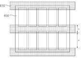
도 10 및 도 11에 도시된 바와 같이, 블랙 매트릭스(610, 650)는 패널의 하부기판에 형성된 가로 격벽과 나란한 방향으로 패널의 상부기판에 형성되므로, 블 랙 매트릭스는 도 8 및 도 9에 도시된 외광차단시트의 상단 또는 하단과 평행하다. 따라서 도 9에서, 패턴부가 외광차단시트의 상단과 이루는 각(Θ1, Θ2, Θ3)은 외광차단시트의 패턴부가 패널에 형성된 블랙 매트릭스와 이루는 각을 나타낸다.As shown in FIGS. 10 and 11, since the
외광차단시트의 패턴부가 패널에 형성된 블랙 매트릭스와 20도 이하의 사이각을 가지고 비스듬히 형성될 때, 모아레 현상을 감소시킬 수 있다. 또한, 패널로 입사되는 외부광이 사용자의 머리 상단에 존재하는 경우가 많은 것을 고려하면, 패턴부와 블랙 매트릭스 사이의 각이 5도 이하일 때 모아레 현상을 방지함과 동시에 적정 개구율을 확보하여 패널 광의 반사 효율을 증가시킬 수 있으며, 외부광을 가장 효과적으로 차단할 수 있다.When the pattern portion of the external light shielding sheet is formed obliquely with an angle of 20 degrees or less with the black matrix formed on the panel, the moiré phenomenon can be reduced. In addition, considering that the external light incident to the panel is often present at the top of the user's head, when the angle between the pattern portion and the black matrix is 5 degrees or less, it prevents moiré phenomenon and at the same time secures an appropriate aperture ratio. It can increase the reflection efficiency and can block the external light most effectively.
도 9는 도 8에 도시된 외광차단시트의 일부분(500)을 확대 도시한 것으로, 일렬로 형성된 패턴부(510, 520, 530, 540, 550, 560)는 서로 평행한 것이 바람직하며, 서로 평행하지 않은 경우에도 패턴부(510, 520, 530, 540, 550, 560)와 블랙 매트릭스의 사이각들은 각각 상기 기재된 범위를 가지는 것이 바람직하다.FIG. 9 is an enlarged view of a
또한, 상기와 같은 이유로 외광차단시트의 패턴부와 패널의 상부 기판에 형성된 버스 전극 또는 하부 기판에 형성된 가로 격벽이 이루는 사이 각(Θ1, Θ2, Θ3)이 20도 이하일때, 모아레 현상을 감소시킬 수 있다. 또한, 패널로 입사되는 외부광이 사용자의 머리 상단에 존재하는 경우가 많은 것을 고려하면, 패턴부와 상기 버스 전극 또는 가로 격벽이 이루는 사이 각(Θ1, Θ2, Θ3)이 5도 이하일 때 모아레 현상을 방지함과 동시에 적정 개구율을 확보하여 패널 광의 반사 효율을 증가시 킬 수 있으며, 외부광을 가장 효과적으로 차단할 수 있다.In addition, when the angle (Θ 1 , Θ 2 , Θ 3 ) between the pattern portion of the external light shielding sheet and the bus electrode formed on the upper substrate of the panel or the horizontal partition wall formed on the lower substrate is 20 degrees or less, the moiré phenomenon Can be reduced. In addition, considering that the external light incident on the panel is often present at the top of the user's head, the angle Θ 1 , Θ 2 , Θ 3 between the pattern portion and the bus electrode or the horizontal partition wall is 5 degrees or less. When the moiré phenomenon is prevented at the same time to secure the appropriate aperture ratio to increase the panel light reflection efficiency, it is possible to block the external light most effectively.
도 8 및 도 9에서는, 패턴부가 외광차단시트의 우측 하단에서 좌측 상단 방향으로 비스듬히 형성되어있으나, 다른 실시예로는 패턴부가 외광차단시트의 좌측 상단에서 우측 하단 방향으로 상기한 바와 같은 각을 가지고 비스듬히 형성되어있을 수도 있다.8 and 9, the pattern portion is formed obliquely in the upper left direction from the lower right side of the external light blocking sheet, but in another embodiment, the pattern portion has the angle as described above in the upper left direction from the upper left of the external light blocking sheet. It may be formed at an angle.
도 10 및 도 11은 패널에 형성된 블랙 매트릭스의 구조에 대한 실시예들을 간략하게 도시한 것이다.10 and 11 briefly illustrate embodiments of the structure of the black matrix formed in the panel.
도 10을 참조하면, 블랙 매트릭스(610)는 하부기판(600)에 형성된 가로 격벽에 중첩되도록 형성될 수 있다. 또한, 도 10에 도시된 바와 같이 블랙 매트릭스(610)는 상부기판에 형성된 스캔 전극 및 서스테인 전극과 중첩되게 형성되어, 스캔 전극 및 서스테인 전극이 블랙 매트릭스(610)에 의해 가려지도록 형성될 수 있다.Referring to FIG. 10, the
이 경우, 블랙 매트릭스(610)의 폭(b)이 200㎛ 내지 400㎛이고, 서로 인접한 블랙 매트릭스 사이의 간격(a)이 300㎛ 내지 600㎛일 때, 디스플레이 영상이 적정 휘도를 가지도록 하기 위한 패널의 개구율을 확보하는 동시에, 외부에서 발생하는 외부광을 흡수하여 반사를 줄여주는 광차단 효율과 상부 기판의 퓨리티 및 콘트라스트를 향상시키는 효율을 최대화할 수 있다.In this case, when the width b of the
도 11을 참조하면, 블랙 매트릭스(650)는 상부기판에 형성된 스캔 전극 및 서스테인 전극(630, 640)과 이격되어 형성될 수 있다.Referring to FIG. 11, the black matrix 650 may be formed to be spaced apart from the scan electrodes and the sustain
이 경우에는, 블랙 매트릭스(650)의 폭(d)이 70㎛ 내지 150㎛이고, 서로 인 접한 블랙 매트릭스 사이의 간격(c)이 500㎛ 내지 800㎛일 때, 디스플레이 영상이 적정 휘도를 가지도록 하기 위한 패널의 개구율을 확보하는 동시에, 외부에서 발생하는 외부광을 흡수하여 반사를 줄여주는 광차단 효율과 상부 기판의 퓨리티 및 콘트라스트를 향상시키는 효율을 최대화할 수 있다.In this case, when the width d of the black matrix 650 is 70 μm to 150 μm and the distance c between adjacent black matrices is 500 μm to 800 μm, the display image has an appropriate brightness. In order to secure the aperture ratio of the panel, the light blocking efficiency of absorbing external light generated from the outside to reduce reflection and the efficiency of improving the purity and contrast of the upper substrate can be maximized.
상기한 바와 같이, 외광차단시트의 패턴부의 패턴과 패널의 상부기판에 형성된 블랙 매트릭스의 패턴이 겹치면서 모아레 현상이 발생할 수 있다.As described above, the moiré phenomenon may occur while the pattern of the pattern portion of the external light blocking sheet overlaps the pattern of the black matrix formed on the upper substrate of the panel.
블랙 매트릭스의 폭이 패턴부 폭(P1)의 3배 내지 15배인 경우, 모아레 현상을 방지함과 동시에, 패널의 적정 개구율을 확보하고 외광 차단 효율을 극대화할 수 있다. 또한, 서로 인접한 두 블랙 매트릭스 사이의 간격이 서로 인접한 두 패턴부 사이 간격(D1)의 4배 내지 12배일 때, 패널 광이 블랙 매트릭스 사이를 통과하여 외광차단시트의 패턴부 경사면에 전반사되 외부로 방출되는 반사 효율을 최적화할 수 있으며, 모아레 현상을 감소시킬 수 있다.When the width of the black matrix is 3 to 15 times the width of the pattern portion P1, the moir phenomenon may be prevented, and the appropriate opening ratio of the panel may be secured and the external light blocking efficiency may be maximized. Further, when the distance between two adjacent black matrices is 4 to 12 times the distance D1 between the two adjacent pattern parts, the panel light passes between the black matrices and is totally reflected on the inclined surface of the pattern part of the external light shielding sheet to the outside. It is possible to optimize the reflection efficiency emitted and to reduce the moiré phenomenon.
도 10에 도시된 경우와 같이 블랙 매트릭스(610)가 스캔 전극 및 서스테인 전극에 중첩되어 형성된 경우에는, 블랙 매트릭스(610)의 폭(b)이 외광차단시트의 패턴부 폭(P1)의 10배 내지 15배일때 모아레 현상을 방지함과 동시에, 패널의 적정 개구율을 확보하고 외광 차단 효율을 극대화할 수 있으며, 서로 인접한 블랙 매트릭스 사이의 간격(a)이 서로 인접한 패턴부 사이 간격의 4배 내지 9배일 때 패널 광의 반사 효율을 최적화할 수 있으며, 모아레 현상을 감소시킬 수 있다.When the
도 11에 도시된 경우와 같이 블랙 매트릭스(650)가 스캔 전극 및 서스테인 전극(630, 640)에 이격되어 형성된 경우에는, 블랙 매트릭스(650)의 폭(d)이 외광 차단시트 패턴부 폭(P1)의 3배 내지 7배일때 모아레 현상을 방지함과 동시에, 패널의 적정 개구율을 확보하고 외광 차단 효율을 극대화할 수 있으며, 서로 인접한 블랙 매트릭스 사이의 간격(c)이 서로 인접한 패턴부 사이 간격의 7배 내지 12배일 때 패널 광의 반사 효율을 최적화할 수 있으며, 모아레 현상을 감소시킬 수 있다.When the black matrix 650 is formed to be spaced apart from the scan electrode and the sustain
도 13은 본 발명에 따른 플라즈마 디스플레이 패널의 상부 기판에 형성된 버스 전극의 구조에 대한 일실시예를 단면도로 도시한 것이다. 13 is a cross-sectional view of an embodiment of a structure of a bus electrode formed on an upper substrate of a plasma display panel according to the present invention.
도 7을 참조하여 설명한 바와 같이 외광차단시트의 서로 인접한 패턴부 사이 간격은 40㎛ 내지 90㎛인 것이 바람직하며, 패널의 상부 기판에 형성된 서로 인접한 두 버스 전극(660, 670) 사이의 간격(a)이 225㎛ 내지 480㎛일때 디스플레이 영상이 적정 휘도를 가지도록 하기 위한 패널의 개구율을 확보하는 동시에 방전 개시 전압을 감소시킬 수 있다. 그에 따라, 서로 인접한 두 버스 전극(660,670) 사이의 간격(a)이 서로 인접한 두 패턴부 사이 간격의 2.5배 내지 12배일때, 패널의 적정 개구율을 확보하고 외광 차단 효율을 극대화할 수 있으며, 패널 광의 반사 효율을 최적화할 수 있다.As described with reference to FIG. 7, the distance between the adjacent pattern parts of the external light blocking sheet is preferably 40 μm to 90 μm, and the distance a between the two
또한, 외광차단시트의 패턴부와 패널의 버스 전극이 겹침에 따라 발생하는 모아레 현상을 감소시키기 위해서는, 서로 인접한 패턴부 사이 간격이 40㎛ 내지 60㎛이고, 서로 인접한 두 버스 전극(660, 670) 사이의 간격(a)이 225㎛ 내지 480㎛인 것이 바람직하다. 따라서 서로 인접한 두 버스 전극(660, 670) 사이의 간격(a)이 서로 인접한 두 패턴부 사이 간격의 4배 내지 10배일때, 패널의 적정 개구율을 확보하고 외광 차단 효율을 극대화할 수 있으며, 패널 광의 반사 효율을 최적 화하는 동시에 모아레 현상을 감소시킬 수 있다.In addition, in order to reduce the moiré phenomenon caused by the overlap between the pattern portion of the external light shielding sheet and the bus electrodes of the panel, the distance between the adjacent pattern portions is 40 μm to 60 μm, and two
도 7을 참조하여 설명한 바와 같이 외광차단시트의 패턴부의 하단 폭은 18㎛ 내지 35㎛인 것이 바람직하며, 패널의 상부 기판에 형성된 버스 전극(660)의 폭(b)은 45㎛ 내지 90㎛일때 패널 구동을 위한 적정 저항 및 커패시턴스를 확보할 수 있으며, 디스플레이 영상이 적정 휘도를 가지도록 하기 위한 패널의 개구율을 확보할 수 있다. 따라서 패널 구동을 위한 적정 저항 및 커패시턴스를 확보할 수 있으며, 디스플레이 영상이 적정 휘도를 가지도록 하기 위한 패널의 개구율을 확보하기 위해, 패턴부의 하단 폭은 버스 전극(660)의 폭(b)의 0.2배 내지 0.8배인 것이 바람직하다.As described with reference to FIG. 7, the bottom width of the pattern portion of the external light blocking sheet is preferably 18 μm to 35 μm, and the width b of the
도 13 및 도 14는 본 발명에 따른 플라즈마 디스플레이 패널의 하부 기판에 형성된 격벽의 구조에 대한 실시예들을 단면도로 도시한 것으로, 격벽은 상부 기판에 형성된 버스 전극과 교차하는 방향으로 형성된 세로 격벽(720) 및 세로 격벽(720)에 교차하는 방향으로 형성된 가로 격벽(700, 710)을 포함한다.13 and 14 illustrate cross-sectional views of embodiments of a structure of a barrier rib formed on a lower substrate of the plasma display panel according to the present invention, wherein the barrier rib is formed in a direction crossing the bus electrode formed on the upper substrate. And
디스플레이 영상의 적정 휘도 및 해상도 확보를 고려하면, 서로 인접한 두 가로 격벽(700, 710) 사이의 간격(c)은 540㎛ 내지 800㎛인 것이 바람직하다. 그에 따라, 패널의 적정 개구율 확보하는 동시에 외광 차단 효과 및 패널 광 반사 효율을 증가시키기 위한 서로 인접한 두 패턴부 사이의 간격이 40㎛ 내지 90㎛인 것을 고려하면, 서로 인접한 두 가로 격벽(700, 710) 사이의 간격(c)이 서로 인접한 두 패턴부 사이의 간격의 6배 내지 20배인 것이 바람직하다.In consideration of securing appropriate brightness and resolution of the display image, the distance c between two adjacent
또한, 서로 인접한 패턴부 사이 간격이 40㎛ 내지 60㎛이고, 서로 인접한 두 가로 격벽(700, 710) 사이의 간격(c)이 600㎛ 내지 700㎛일 때, 외광차단시트의 패턴부와 패널의 가로 격벽이 겹침에 따라 발생하는 모아레 현상을 감소시킬 수 있다. 따라서 서로 인접한 두 가로 격벽(700, 710) 사이의 간격(c)이 서로 인접한 두 패턴부 사이의 간격의 10배 내지 17.5배일때, 외부에서 발생하는 외부광을 흡수하여 반사를 줄여주는 광차단 효율과 상부 기판의 퓨리티 및 콘트라스트를 향상시키는 효율을 최대화하는 동시에 모아레 현상을 감소시킬 수 있다.Further, when the distance between the pattern portions adjacent to each other is 40 μm to 60 μm, and the distance c between the two
도 7을 참조하여 설명한 바와 같이 외광차단시트의 패턴부의 하단 폭은 18㎛ 내지 35㎛인 것이 바람직하며, 가로 격벽(700)의 상단 폭(d)이 45㎛ 내지 90㎛일때 디스플레이 영상이 적정 휘도를 가지도록 하기 위한 패널의 개구율을 확보할 수 있다. 따라서 디스플레이 영상이 적정 휘도를 가지도록 하기 위한 패널의 개구율을 확보하고, 외광차단시트의 패턴부와 패널의 가로 격벽이 겹침에 의해 발생하는 모아레 현상을 감소시키기 위해, 패턴부의 하단 폭은 가로 격벽(700)의 상단 폭(d)의 0.2배 내지 0.8배인 것이 바람직하다.As described with reference to FIG. 7, the bottom width of the pattern portion of the external light blocking sheet is preferably 18 μm to 35 μm, and when the top width d of the
도 14에 도시된 바와 같이, 격벽(800, 810) 중 일부분의 폭이 다른 부분과 상이할 수도 있다. 격벽이(800, 810)이 도 14에 도시된 바와 같은 구조를 가지는 경우에는, 서로 인접한 두 가로 격벽(800, 810) 사이의 간격(c)과 가로 격벽(800)의 상단 폭(d)은 격벽의 직선 부분을 기준으로 정의될 수 있다. As shown in FIG. 14, a width of a portion of the
도 15 내지 도 19는 외광차단시트의 패턴부 형상에 대한 실시예들을 단면도로 도시한 것이다.15 to 19 illustrate embodiments of the pattern portion of the exterior light shielding sheet in cross-sectional view.
도 15를 참조하면, 패턴부(900)는 좌우 비대칭 형상으로 형성될 수도 있다. 즉, 패턴부(900)의 좌우 경사면 면적이 상이하거나, 좌우 경사면 각각이 하단과 이루는 각이 서로 상이할 수 있다. 일반적으로 외광을 발생시키는 물체들은 패널의 상측에 위치하므로, 외광은 일정한 각도 범위 내에서 패널의 상측으로부터 패널로 입사된다. 따라서, 외광 흡수 효과를 증가시키고, 패널로부터 방출되는 광의 반사율을 증가시키기 위해, 패턴부(900)의 두 경사면 중 외광이 입사되는 상측 경사면의 기울기를 하측 경사면의 기울기보다 완만하게 할 수 있다. 즉, 패턴부(900)의 두 경사면 중 상측 경사면의 기울기가 하측 경사면의 기울기보다 작게 할 수 있다.Referring to FIG. 15, the
도 16을 참조하면, 패턴부(910)는 사다리꼴 형상을 가질 수도 있으며, 그러한 경우 상단의 폭(P2)이 하단의 폭(P1)보다 작게 형성된다. 또한, 패턴부(910) 상단의 폭(P2)은 10㎛ 이하일 수 있으며, 그에 따라 하단 폭(P1)과의 관계에서 외광의 흡수 및 패널 광의 반사를 효과적으로 할 수 있는 경사면 기울기를 형성할 수 있다.Referring to FIG. 16, the
도 17 내지 도 19에 도시된 바와 같이, 외광차단시트의 패턴부(920, 930, 940)의 형상은 좌우 경사면이 소정의 곡률을 가지는 곡선 형태일 수도 있다. 이 경우, 비스듬히 입사되는 외광의 차단 효과를 향상시키기 위해, 패턴부(920, 930, 940) 경사면의 기울기의 변화량은 하단에서 상단으로 갈수록 감소되는 것이 바람직하다.17 to 19, the shape of the
또한, 도 17 내지 도 19에 도시된 패턴부의 형상에 대한 실시예들에 있어서, 패턴부의 모서리 부분이 소정의 곡률을 가지는 곡선 형태를 가질 수도 있다.In addition, in embodiments of the shape of the pattern portion illustrated in FIGS. 17 to 19, the corner portion of the pattern portion may have a curved shape having a predetermined curvature.
도 20은 하단이 오목한 형태를 가지는 패턴부의 형상에 대한 실시예를 단면 도로 도시한 것이다.20 is a sectional view showing an embodiment of the shape of the pattern portion having a concave shape at the bottom.
도 20에 도시된 바와 같이, 패턴부의 하단(1015)이 가운데가 동그스름하게 폭 패거나 들어가 있는 오목한 형태를 가지도록 함으로써, 패널로부터 방출되는 광이 패턴부의 하단(1015)에서 반사됨에 따라 발생하는 영상의 번짐 현상을 감소시킬 수 있으며, 외광차단시트가 다른 기능성 시트 또는 패널에 부착되는 경우 접착 부위의 면적을 증가시킴으로써 접착력을 향상시킬 수 있다.As shown in FIG. 20, the
즉, 중심 부분에서의 높이가 최외곽 부분에서의 높이보다 작은 값을 가지도록 패턴부(1010)를 형성함으로써, 오목한 형태의 하단(1015)을 포함하는 패턴부(1010)를 형성할 수 있다.That is, by forming the
패턴부(1010)는 베이스부(1000)에 형성된 홈에 광흡수 물질 등을 채움에 의해 형성될 수 있는데, 상기 베이스부(1000)에 형성된 홈 중 일부분이 패턴부(1010)를 이루는 광흡수 물질로 채워지고, 나머지 부분은 빈공간으로 남겨질 수 있다. 그에 따라, 패턴부의 하단(1015)이 가운데 부분이 내부로 인입되어 있는 오목한 형태를 가질 수 있다.The
도 21에 도시된 바와 같이 패턴부(1030)의 하단이 평평한 경우, 패널로부터 방출되어 패턴부(1030)의 하단으로 비스듬히 입사되는 광은 패널 방향으로 반사될 수 있다. 상기와 같이 패널 방향으로 반사되는 패널 광에 의해 특정 위치에 디스플레이되어야할 영상이 상기 특정 위치의 주변에 디스플레이됨으로써, 영상 번짐 현상이 발생되어 디스플레이 영상의 선명도를 저하시킬 수 있다.As shown in FIG. 21, when the bottom of the
도 22을 참조하면, 오목한 형태를 가지는 패턴부(1010)의 하단으로 비스듬히 입사되는 광의 입사각(θ2)은 도 21에 도시된 평평한 패턴부(1030)의 하단에 입사되는 입사각(θ1)보다 작아지게 된다. 따라서 도 21에 도시된 평평한 패턴부(1030)의 하단에서 반사되는 패널 광이 도 22에 도시된 오목한 형태를 가지는 패턴부(1010)의 하단에서는 패턴부(1010) 내부로 흡수될 수 있다. 그에 따라 디스플레이 영상의 번짐 현상을 감소시켜 영상의 선명도를 향상시킬 수 있다.Referring to FIG. 22, an incident angle θ2 of light incident obliquely to the lower end of the
도 23은 하단이 오목한 패턴부를 포함하는 외광차단시트의 구조에 대한 실시예를 단면도로 도시한 것으로, 패턴부(1110)의 하단을 오목한 형태로 하여 관찰자 측에 배치한 것이다.FIG. 23 is a cross-sectional view showing an embodiment of a structure of an external light shielding sheet including a pattern portion having a bottom concave. The bottom portion of the
도 23을 참조하면, 관찰자 측에 배치된 패턴부(1110)의 하단을 오목한 형태로 함으로써, 패턴부(1110) 하단에서 흡수되는 외광의 입사각 범위를 확대시킬 수 있다. 즉, 패턴부(1110)의 하단을 오목한 형태로 하는 경우, 외광의 패턴부(1110) 하단으로의 입사각을 크게 할 수 있으며, 그로 인해 외광 흡수 효과를 향상시킬 수 있다.Referring to FIG. 23, the incidence angle range of external light absorbed by the lower end of the
도 24는 하단이 오목한 형태를 가지는 패턴부의 형상에 대한 실시예를 단면도로 도시한 것이다. 다음의 표 1은 패턴부(1210)의 하단을 오목한 형태로 형성함으로써 생기는 홈의 깊이(a)와 패턴부(1210)의 하단 폭(d)에 따른 디스플레이 영상의 번짐 현상 감소 여부를 실험한 결과로서, 하단이 평평한 패턴부를 가지는 외광차단시트가 배치된 플라즈마 디스플레이 패널에 비해 영상의 번짐 현상이 감소되는지 여부를 실험한 결과이다.24 is a sectional view showing an embodiment of the shape of the pattern portion having a concave shape at the bottom. Table 1 below shows the results of experiments on whether or not the blurring phenomenon of the display image is reduced according to the depth (a) of the groove formed by forming the lower end of the
표 1에 나타난 바와 같이, 패턴부(1210)의 하단에 형성된 홈의 깊이(a)가 1.5㎛ 내지 7.0㎛일 때, 디스플레이 영상의 번짐 현상을 감소시켜 영상의 선명도를 향상시킬 수 있다.As shown in Table 1, when the depth (a) of the groove formed in the lower end of the
또한, 외부 충격 등에 의한 패턴부(1210)의 파손 방지 및 패턴부(1210) 형성 공정의 용이성을 고려하면, 패턴부(1210)의 하단에 형성된 홈의 깊이(a)는 2㎛ 내지 5㎛인 것이 바람직하다.In addition, considering the prevention of damage to the
도 7를 참조하여 설명한 바와 같이 패턴부(1210)의 하단 폭(d)이 18㎛ 내지 35㎛일 때 패널 광 방출을 위한 개구율을 확보하고 외광 차단 효율을 극대화할 수 있으므로, 패턴부(1210)의 하단 폭(d)은 패턴부(1210)의 하단에 형성된 홈의 깊이(a)의 3.6배 내지 17.5배인 것이 바람직하다.As described with reference to FIG. 7, when the bottom width d of the
한편, 패턴부(1210)의 높이(c)가 80㎛ 내지 170㎛일때 외광의 흡수 및 패널 광의 반사를 효과적으로 할 수 있는 경사면 기울기를 형성할 수 있으므로, 패턴부(1210)의 높이(c)가 패턴부(1210)의 하단에 형성된 홈의 깊이(a)의 16배 내지 85배인 것이 바람직하다.On the other hand, when the height c of the
또한, 외광차단시트의 두께(b)가 100㎛ 내지 180㎛일 때 패널 광의 원활한 투과와 외광의 효과적인 흡수 및 차단을 달성할 수 있고 시트의 견고성을 확보할 수 있으므로, 외광차단시트의 두께(b)는 패턴부(1210)의 하단에 형성된 홈의 깊이(a)의 20배 내지 90배인 것이 바람직하다.In addition, when the thickness (b) of the external light shielding sheet is 100 μm to 180 μm, smooth transmission of panel light and effective absorption and blocking of external light can be achieved, and the firmness of the sheet can be secured. ) Is preferably 20 to 90 times the depth (a) of the groove formed in the lower end of the
도 25를 참조하면, 패턴부(1230)는 사다리꼴 형상을 가질 수도 있으며, 그러한 경우 상단의 폭(e)이 하단의 폭(d)보다 작게 형성되는 것이 바람직하다. 또한, 패턴부(1230) 상단의 폭(e)은 10㎛ 이하일 때, 하단 폭(d)과의 관계에서 외광의 흡수 및 패널 광의 반사를 효과적으로 할 수 있는 경사면 기울기를 형성할 수 있다. 이 경우에도, 패턴부(1230) 하단에 형성된 홈의 깊이(a)와 패턴부(1230) 하단 폭(d) 사이의 관계는 도 24를 참조하여 설명한 것과 동일할 수 있다.Referring to FIG. 25, the
도 26은 외광차단시트의 두께와 패턴부의 높이 사이의 관계를 설명하기 위해 외광차단시트의 구조를 단면도로 도시한 것이다.FIG. 26 is a cross-sectional view of the structure of the external light shielding sheet to explain the relationship between the thickness of the external light blocking sheet and the height of the pattern portion.
도 26을 참조하면, 패턴부를 포함하는 외광차단시트의 견고성을 확보하는 동시에 화상을 표시하기 위해 패널로부터 방출되는 가시광의 투과율을 확보하기 위해, 외광차단시트의 두께(T)는 100㎛ 내지 180㎛인 것이 바람직하다.Referring to FIG. 26, the thickness T of the external light blocking sheet is 100 μm to 180 μm to secure the robustness of the external light blocking sheet including the pattern portion and to secure the transmittance of visible light emitted from the panel to display an image. Is preferably.
외광차단시트에 구비되는 패턴부의 높이(h)가 80㎛ 내지 170㎛일 때, 상기 패턴부의 제조가 가장 용이하며, 외광차단시트의 적절한 개구율을 확보할 수 있고, 외광 차단 효과 및 패널로부터 방출되는 광의 반사 효과를 최대화할 수 있다.When the height h of the pattern portion provided in the external light shielding sheet is 80 μm to 170 μm, the pattern part is most easily manufactured, and an appropriate opening ratio of the external light blocking sheet can be ensured, and the external light blocking effect and the light emitted from the panel The reflection effect of the light can be maximized.
패턴부의 높이(h)는 외광차단시트의 두께(T)에 따라 가변 될 수 있다. 일반적으로 패널로 입사되어 명실콘트라스트 저하에 영향을 주는 외광은 주로 패널의 위치보다 상측에 위치하게 된다. 따라서 일정한 범위의 입사각(θ)을 가지도 패널로 입사되는 외광을 효과적으로 차단하기 위해, 패턴부의 높이(h)와 외광차단시트의 두께(T)의 비율은 일정 범위 내의 값을 가지는 것이 바람직하다.The height h of the pattern portion may vary depending on the thickness T of the external light shielding sheet. In general, external light incident on the panel and affecting bright room contrast is mainly located above the position of the panel. Therefore, in order to effectively block external light incident on the panel even with a predetermined angle of incidence θ, the ratio of the height h of the pattern portion to the thickness T of the external light shielding sheet preferably has a value within a certain range.
패턴부의 높이(h)가 증가할수록 패턴부 상단 부분의 베이스부 두께가 얇아져 절연 파괴가 발생할 수 있으며, 패턴부의 높이(h)가 감소할수록 일정 범위 내의 각도를 가지는 외광이 패널로 입사되어 외광 차단이 제대로 차단되지 않을 수 있다.As the height (h) of the pattern portion increases, the thickness of the base portion of the upper portion of the pattern portion may become thinner, and insulation breakage may occur. It may not be blocked properly.
다음의 표 2는 외광차단시트의 두께(T)와 패턴부의 높이(h)에 따라 외광차단시트의 절연 파괴 및 외광 차단 효과를 실험한 결과이다.Table 2 below shows the results of experiments of insulation breakdown and external light blocking effects of the external light blocking sheet according to the thickness (T) of the external light blocking sheet and the height (h) of the pattern portion.
표 2를 참조하면, 외광차단시트의 두께(T)가 120㎛일 경우, 패턴부의 높이(h)가 115㎛ 이상으로 형성되면 패턴부가 절연 파괴될 위험이 있어 제품의 불량율이 증가할 수 있다. 패턴부의 높이(h)가 115㎛ 이하로 형성되면 패턴부가 절연 파괴될 우려가 없어 외광차단시트의 불량율을 감소시킬 수 있다. 그러나, 패턴부의 높이가 85㎛이하로 형성될 때에는 패턴부에 의해 외부광이 차단되는 효율이 감소될 수 있으며, 60㎛ 이하로 형성되는 경우에는 외광이 패널로 입사될 수 있다. 그에 따라, 패턴부의 높이(h)가 90㎛ 내지 110㎛일 때, 외광차단시트의 외광 차단 효율을 증가시키는 동시에 불량율을 감소시킬 수 있다.Referring to Table 2, when the thickness T of the external light shielding sheet is 120 μm, when the height h of the pattern part is formed to be 115 μm or more, there is a risk that the pattern part is insulated and destroyed, thereby increasing the defective rate of the product. If the height h of the pattern portion is formed to be 115 μm or less, there is no fear that the pattern portion will be insulated and broken, thereby reducing the defective rate of the external light shielding sheet. However, when the height of the pattern portion is formed to be 85 μm or less, the efficiency of blocking external light by the pattern portion may be reduced, and when formed to 60 μm or less, external light may be incident on the panel. Accordingly, when the height h of the pattern portion is 90 μm to 110 μm, the external light blocking efficiency of the external light shielding sheet may be increased and the defective rate may be reduced.
또한, 외광차단시트의 두께(T)가 패턴부 높이(h)의 1.01배 내지 2.25배일 때, 패턴부 상단 부분의 절연 파괴를 방지할 수 있으며, 외광이 패널로 입사되는 것을 방지할 수 있다. 또한, 절연 파괴 및 외광의 패널 입사를 방지함과 동시에, 패널로부터 방출되는 광의 반사량을 증가시키고 시야각을 확보하기 위해서는, 외광차단시트의 두께(T)가 패턴부 높이(h)의 1.01배 내지 1.5배일 수 있다.In addition, when the thickness T of the external light shielding sheet is 1.01 to 2.25 times the height of the pattern portion, insulation breakdown of the upper portion of the pattern portion may be prevented, and external light may be prevented from entering the panel. In addition, in order to prevent dielectric breakdown and external light incident on the panel, and to increase the amount of reflection of light emitted from the panel and to secure a viewing angle, the thickness T of the external light shielding sheet is 1.01 times to 1.5 times the height of the pattern portion. It may be a boat.
다음의 표 3은 외광차단시트의 패턴부 하단 폭과 패널의 상부 기판에 형성되는 버스 전극의 폭의 비율에 따라 모아레 현상 발생 여부 및 외광 차단 효과를 실험한 결과로서, 버스 전극의 폭이 70㎛인 경우이다.Table 3 below shows the results of experiments on whether moiré occurred and external light blocking effect according to the ratio of the width of the bottom of the pattern portion of the external light blocking sheet to the width of the bus electrode formed on the upper substrate of the panel. If
표 3을 참조하면, 패턴부 하단의 폭이 버스 전극 폭의 0.2배 내지 0.5배일 때, 모아레 현상을 감소시킴과 동시에 패널로 입사되는 외광을 감소시킬 수 있다. 또한, 모아레 현상을 방지하고 외광을 효과적으로 차단하는 동시에, 패널 광의 방출을 위한 개구율을 확보하기 위해서는, 패턴부 하단의 폭이 버스 전극 폭의 0.25배 내지 0.4배인 것이 바람직하다.Referring to Table 3, when the width of the bottom of the pattern portion is 0.2 times to 0.5 times the width of the bus electrode, it is possible to reduce the moiré phenomenon and at the same time reduce the external light incident on the panel. In addition, in order to prevent moiré phenomenon and effectively block external light, and to secure an aperture ratio for emitting panel light, the width of the lower end of the pattern portion is preferably 0.25 times to 0.4 times the width of the bus electrode.
다음의 표 4는 외광차단시트의 패턴부 하단 폭과 패널의 하부 기판에 형성되는 세로 격벽의 폭의 비율에 따라 모아레 현상 발생 여부 및 외광 차단 효과를 실험한 결과로서, 세로 격벽의 폭이 50㎛인 경우이다.Table 4 below shows the results of experiments on the occurrence of moiré phenomenon and external light blocking effect according to the ratio of the width of the bottom of the pattern portion of the external light blocking sheet to the width of the vertical partition formed on the lower substrate of the panel. If
표 4를 참조하면, 패턴부의 하단 폭이 세로 격벽의 상단 폭의 0.3배 내지 0.8배일 때, 모아레 현상을 감소시키는 동시에 패널로 입사되는 외광을 감소시킬 수 있다. 또한, 모아레 현상을 방지하고 외광을 효과적으로 차단하는 동시에, 패널 광의 방출을 위한 개구율을 확보하기 위해서는, 패턴부의 하단 폭이 세로 격벽의 상단 폭의 0.4배 내지 0.65배인 것이 바람직하다.Referring to Table 4, when the bottom width of the pattern portion is 0.3 times to 0.8 times the top width of the vertical partition wall, it is possible to reduce the moiré phenomenon and at the same time reduce the external light incident on the panel. In addition, in order to prevent moiré phenomenon and effectively block external light, and to secure an aperture ratio for emitting panel light, it is preferable that the bottom width of the pattern portion is 0.4 times to 0.65 times the top width of the vertical partition wall.
도 27 내지 도 30은 본 발명에 따른 필터의 구조에 대한 실시예들을 단면도로 도시한 것으로, 플라즈마 디스플레이 패널의 전면에 형성되는 필터는 AR/NIR 시트, EMI 차폐시트, 외광차단시트, 광특성시트 등을 포함할 수 있다.27 to 30 are sectional views showing embodiments of the structure of the filter according to the present invention. The filter formed on the front surface of the plasma display panel includes an AR / NIR sheet, an EMI shield sheet, an external light shield sheet, and an optical sheet. And the like.
도 27 및 도 28을 참조하면, AR/NIR 시트(1310)는 투명한 플라스틱 재질로 이루어진 베이스시트(1313)의 전면에 외부로부터 입사되는 빛이 반사되는 것을 방지하여 눈부심 현상을 감소시키는 기능이 있는 AR(Anti-Reflection)층(1311)이 부착되고, 후면에는 패널로부터 방사되는 근적외선을 차폐하여 리모콘 등과 같이 적외선을 이용하여 전달되는 신호들이 정상적으로 전달될 수 있도록 하는 NIR(Near Infrared) 차폐시트(1312)이 부착된다.Referring to FIGS. 27 and 28, the AR /
EMI 차폐시트(1320)는 패널로부터 방사되는 EMI(Electromagnetic Interference)가 외부로 방출되는 것을 방지하는 시트로서, 본 발명에서는 스퍼터링(SPUTTERING)방법으로 형성된 적어도 3개의 박막층이 한 셋트를 이루고, 상기 한 셋트가 반복되어 적층되는 구조를 가진다.
상기 스퍼터링 방법이란, 금속판에 아르곤 등의 불활성 원소를 부딪쳐서 금속 분자를 쫓아낸 후 표면에 막을 부착하는 기술로서 박막층의 제조방법 중 하나이다. 진공이 유지된 챔버(Chamber) 내에 스퍼터링 기체로 불활성 물질인 아르곤(Ar)가스를 흘려주면서 타겟에 직류 전원을 인가하면, 증착하고자 하는 기판과 타겟사이에서 플라즈마가 발생한다. 즉, 상기 아르곤 가스가 양이온으로 이온화되고, 이는 직류전류계에 의해 음극으로 가속되어 타겟 표면과 충돌하며, 이로 인해 타겟물질의 원자가 표면으로부터 탈출하여 기판에 박막층을 형성하게 된다.The sputtering method is one of the methods for producing a thin film layer as a technique of striking an inert element such as argon on a metal plate to drive out metal molecules and then attaching a film to the surface. When DC power is applied to a target while argon (Ar) gas, which is an inert material, is flowed into a chamber where vacuum is maintained, a plasma is generated between the substrate to be deposited and the target. That is, the argon gas is ionized with a cation, which is accelerated to the cathode by a direct current ammeter and collides with the target surface, whereby atoms of the target material escape from the surface to form a thin film layer on the substrate.
이와 같이 스퍼터링 방법으로 EMI차폐시트가 형성되면, 메쉬타입의 EMI차폐시트에 비해 모아레 현상이 현저하게 감소될 수 있다. 즉, 모아레 현상은 특정 패턴이 규칙적으로 반복됨에 따라 발생되는 현상으로서 화질을 저하시키는 주요 원인으로 지적되고 있으나, 본 발명에서와 같이 스퍼터링 방법으로 형성된 EMI차폐시트에서는 패턴이 형성되지 아니하므로 모아레 현상이 발생되지 않는 것이다. As such, when the EMI shielding sheet is formed by the sputtering method, the moiré phenomenon may be significantly reduced as compared to the EMI shielding sheet of the mesh type. That is, the moiré phenomenon is a phenomenon that occurs when a specific pattern is regularly repeated, but has been pointed out as a main cause of deterioration in image quality, but the moiré phenomenon is not formed in the EMI shielding sheet formed by the sputtering method as in the present invention. It doesn't happen.
이러한 본 발명의 EMI차폐시트에는 적어도 하나의 적층셋트가 반복되는 구조이며, 상기 하나의 적층셋트는 유전체층, 보호층 및 금속층을 포함한다. 각 층의 적층순서는 도면에 의해 한정되지 않으나, 가장 투명한 박막층이 외면을 이루도록 배치되는 것이 빛의 투과율 측면에서 바람직할 것이다. The EMI shield sheet of the present invention has a structure in which at least one lamination set is repeated, and the one lamination set includes a dielectric layer, a protective layer, and a metal layer. The stacking order of each layer is not limited by the drawings, but it is preferable to arrange the most transparent thin film layers to form the outer surface in terms of light transmittance.
아울러, 상기 적층셋트는 수회 반복될 수 있으며, 적층되는 박막층이 많을수록 저항치가 높아지게 되므로 EMI차폐효율이 증가하게 될 것이다. 반면, 빛의 투과율은 저하되고 생산비용은 증가하게 되므로 상기 셋트가 반복되는 횟수는 소정의 횟수만큼 제한되는 것이 바람직하다. In addition, the lamination set may be repeated several times, and the more the thin film layer is laminated, the higher the resistance value will increase the EMI shielding efficiency. On the other hand, since the light transmittance is lowered and the production cost is increased, the number of times the set is repeated is preferably limited to a predetermined number of times.
본 발명에서는 상기 셋트가 3회만큼 반복되는 것을 예시하는데, 그 이유는 적층이 반복됨에 따른 간섭현상으로 인해 투과되는 빛이 소멸되지 아니하고, 패널에서 방출되는 EMI를 효율적으로 차폐할 수 있기 때문이다. 물론, 상기 셋트가 3회 반복되더라도 상기 유전체층, 보호층 및 금속층 중 어느 하나의 층이 추가될 수 있는바, 스퍼터링 방식에 의해 적층되는 총 박막층은 9개(3X3) 내지 15개(4X3+3)가 될 것이다. . In the present invention, the set is repeated three times, since the transmitted light does not disappear due to the interference caused by the lamination, and the EMI emitted from the panel can be effectively shielded. Of course, even if the set is repeated three times, any one of the dielectric layer, the protective layer, and the metal layer may be added, and thus the total thin film layers stacked by the sputtering method are 9 (3X3) to 15 (4X3 + 3). Will be. .
통상적으로 외부광원은 실내나 외부에서나 관찰자의 머리 상단에 존재하는 경우가 제일 많다. 이러한 외부광을 효과적으로 차단하여 플라즈마 디스플레이 패널의 블랙영상을 더욱 어둡게 표현될 수 있도록 하는 외광차단시트(1330)가 부착된다.Typically, the external light source is most often present at the top of the observer's head, indoors or outdoors. The external
이와 같은 AR/NIR 시트(1310), EMI 차폐시트(1320), 외광차단시트(1330) 사이에는 점착제(1340)가 층을 이루고 있어, 각각의 시트들(1310, 1320, 1330) 및 필터(1300)가 패널의 전면에 견고하게 부착될 수 있도록 한다. 또한, 각각의 시트들(1310, 1320, 1330) 사이에 포함된 베이스시트의 재질은 필터(1300) 제작의 용이성을 고려하여 실질적으로 동일한 재질을 사용하는 것이 바람직하다.The adhesive 1340 forms a layer between the AR /
한편, 도 27에서는 AR/NIR 시트(1310), EMI 차폐시트(1320), 외광차단시트(1330)의 순으로 적층되어 있으나, 도 28에 도시된 바와 같이 AR/NIR 시트(1310), 외광차단시트(1330), EMI 차폐시트(1320)의 순으로 적층될 수 있듯이 각 시트의 적층순서는 당업자에 의하여 다르게 적층될 수 있을 것이다. 또한, 도시된 시트들(1310, 1320, 1330) 중 적어도 어느 한 층이 생략될 수도 있을 것이다.Meanwhile, in FIG. 27, the AR /
도 29 및 도 30을 참조하면, 패널의 전면에 형성되는 필터(1400)는 AR/NIR 시트(1410), EMI 차폐시트(1430) 및 외광차단시트(1440) 이외에 광특성시트(1420)를 더 포함할 수 있다. 광특성시트(1420)는 패널로부터 입사되는 광의 색온도 및 휘도 특성을 개선시키며, 투명한 플라스틱 재질로 이루어진 베이스시트(1422)의 전면 또는 후면에 소정의 염료와 점착제로 이루어진 광특성층(1421)이 적층된다.29 and 30, the
도 27 내지 도 30에 도시된 베이스 시트들 중 적어도 하나의 베이스시트가 생략될 수도 있고, 상기 베이스 시트들 중 어느 하나는 플라스틱 재질이 아닌 견고한 글라스(Glass)가 사용되어 패널을 보호하는 기능을 향상시킬 수 있다. 상기 글라스는 패널로부터 소정 간격을 가지고 이격되어 형성되는 것이 바람직하다.At least one of the base sheets shown in FIGS. 27 to 30 may be omitted, and any one of the base sheets may be made of hard glass, not plastic, to protect the panel. You can. The glass is preferably formed spaced apart from the panel at a predetermined interval.
또한, 본 발명에 따른 필터는 확산 시트를 더 포함할 수 있다. 확산 시트는 광이 균일한 밝기를 유지하도록 입사되는 광을 확산시켜주는 역할을 한다. 그에 따라, 확산 시트는 패널로부터 방출되는 광을 균일하게 확산시켜 디스플레이 화면의 상하 시야각을 넓히고, 외광차단시트 등에 형성된 패턴을 은폐할 수 있다. 또한, 확산 시트는 상하 시야각에 해당하는 방향으로 광을 집광하여 정면 휘도를 균일하게 하는 동시에 향상시킬 수 있으며, 대전 방지성을 향상시킬 수 있다.In addition, the filter according to the present invention may further include a diffusion sheet. The diffusion sheet serves to diffuse the incident light so that the light maintains uniform brightness. Accordingly, the diffusion sheet uniformly diffuses the light emitted from the panel, thereby widening the vertical viewing angle of the display screen, and concealing the pattern formed in the external light blocking sheet or the like. In addition, the diffusion sheet can condense light in the direction corresponding to the vertical viewing angle to make the front luminance uniform and at the same time improve antistatic property.
확산 시트는 투과형 또는 반사형 확산 필름 등이 사용될 수 있으며, 일반적으로 폴리머(polymer) 재료의 베이스시트에 작은 유리 구슬 알갱이들이 혼합된 형태를 가질 수 있다. 또한, 확산 시트의 베이스시트로 고순도 아크릴 수지(PMMA)가 이용될 수 있으며, 고순도 아크릴 수지(PMMA)를 이용하는 경우 시트의 두께가 두꺼운 반면 내열성이 좋아 발열이 많은 대형 디스플레이 장치에 이용될 수 있다.The diffusion sheet may be a transmissive or reflective diffusion film and the like, and generally may have a form in which small glass bead grains are mixed with a base sheet of a polymer material. In addition, high purity acrylic resin (PMMA) may be used as the base sheet of the diffusion sheet, and when the high purity acrylic resin (PMMA) is used, the sheet may have a thick thickness but good heat resistance, and thus may be used in a large display device having high heat generation.
도 31 및 도 32는 상기 EMI차폐시트(1320,1430)의 구조가 도시된 단면도로서, 도 27에 관한 설명에서 제시한 적층셋트의 구조가 상이한 실시예를 도시한 것이다. 31 and 32 are cross-sectional views illustrating the structures of the
보다 상세하게 한 셋트를 이루는 각 층에 관해 살펴보면, 상기 유전체층(1321)은 니오브 산화물(Nb2O5)을 포함하여 구성된다. 물론, 이외의 Ti, Cr 또는 Zr와 같은 다른 원소 성분도 함유될 수 있음은 물론이다. Looking at each layer forming a set in more detail, the
상기 복수 유전체층(1321)의 두께(T1,T1',T1")는 50nm 내지 80nm의 범위로 형성될 수 있고, 특히 전면기판과 인접하여 배치되는 유전체층의 경우 그 두께가 얇게 형성되는 것이 바람직하다. 그 이유는 기판과 가장 인접한 유전체층의 두께가 얇을수록 가시광 반사율을 감소시키고 낮은 반사율을 얻을 수 있는 파장 범위를 증가시키기 때문이다.The thicknesses T1, T1 ′, and T1 ″ of the plurality of
상기 유전체층(1321) 상에는 ZnO 또는 ITO를 주성분으로 하는 보호층(1322)이 형성된다. 상기 보호층은 EMI를 차폐하기 위한 금속층(1323)을 보호하여 내구성을 향상시키는 동시에, 상기 금속층에 의해 나타나는 전기전도성을 증진시켜 전자파 차폐 성능을 향상시킨다.A
아울러, 상기 보호층(1322)은 금속층(1323) 및 유전체층(1321) 사이의 계면에서 발생되는 표면 플라즈몬의 형성을 억제하여 플라즈몬에 의한 광흡수로 인해 발생하는 가시광 손실을 감소시킨다. 동시에, 가시광 반사율을 감소시키고 저반사율이 얻어질 수 있는 파장 대역을 증가시키는 역할을 하게 되므로 도 31에 도시된 구조에서 최외면을 이루도록 추가적으로 적층될 수 있으며, 도 32에 도시된 실시예와 같이 하부 외면을 이루도록 적층순서를 달리할 수 있다. In addition, the
이를 위해 상기 복수 보호층(1322)의 두께(T2,T2',T2")는 70nm 내지 100nm이내로 형성되며, ZnO 이외에도 Al 또는 Al2O3가 소량 포함되어 있는 산화물(이하, AZO라 함)을 포함하여 형성된다. To this end, the thickness of the plurality of protective layers 1322 (T2, T2 ', T2 ") is formed within 70nm to 100nm, and the oxide containing a small amount of Al or Al 2 O 3 in addition to ZnO (hereinafter referred to as AZO) It is formed to include.
상기 보호층(1322) 상에는 전기전도성을 가지는 금속층(1323)이 형성되며, 금속층은 주로 연성 및 전기전도성이 우수하고, 박막 형성시에도 전기전도성을 유지하는 Ag 또는 상기 Ag가 90% 이상인 합금으로 이루어진다. 또한, 은은 가격이 저렴하고 다른 금속에 비하여 가시광 흡수가 적어 투명한 박막을 얻기가 용이하다는 장점이 있다. The
이러한 금속층(1323)의 총 두께(T3,T3',T3")는 80nm 내지 120nm이내로 형성되고, 상기 유전체층(1321)과 같은 이유로 기판과 가장 인접하게 배치되는 금속층은 다른 금속층 두께에 비해 얇게 형성되는 것이 바람직하다. 그 이유는 가시광 반사율을 감소시키고 저반사율을 얻을 수 있는 파장 대역을 증가시키기 때문이다. The total thickness (T3, T3 ', T3 ") of the
이와 같이 도 31의 실시예의 EMI차폐시트(1321,1430)는 유전체층(1321), 보호층(1322), 금속층(1323)의 순서로 적층되는 구조를 가지며, 이러한 구조가 한 셋트가 되어 3회 반복된 것을 예시하였으나 반복횟수는 도면에 의해 한정되지 아니한다. 아울러, 외면에는 가장 투명한 박막층이 추가적으로 배치될 수 있음은 이미 기재한 바와 같다. As described above, the
이와 같이 스퍼터링 방식으로 형성된 박막층이 적층됨에 따른 EMI 차폐시트의 두께(Te)는 200 내지 300 nm이어야 패널에서 방출되는 EMI 차폐가 가능한 저항치를 가지게 되고, 필터를 이루는 다른 시트와 결합했을 때 박형화를 이루면서 광투과율을 유지할 수 있게 된다. Thus, the thickness (Te) of the EMI shielding sheet according to the stacking of the thin film layer formed by the sputtering method has a resistance value capable of shielding the EMI emitted from the panel at a thickness of 200 to 300 nm, and when combined with other sheets forming the filter, it becomes thinner. The light transmittance can be maintained.
상기 EMI차폐시트(1320,1430)를 이루는 복수의 박막층 두께에 관한 수치범위를 고려해 볼 때, 유전체층의 두께가 가장 얇고, 금속층의 두께가 가장 두껍다는 것을 도출할 수 있으며, 보호층의 두께는 유전체층 두께 대비 1 내지 1.5배 이내이고, 금속층의 두께는 유전체층 두께 대비 1.3 내지 2배이다. Considering the numerical range of the thicknesses of the plurality of thin film layers constituting the
도 32의 실시예에서는 한 셋트를 이루는 박막층이 유전체층(1321), 금속층(1323) 그리고 상기 금속층의 양면에 각각 적층되는 보호층(1322,1324)으로 구성되는 점이 상이하며, 그 이외의 중복되는 구성요소에 대한 설명은 도 31의 실시예에 관한 설명으로 대체한다. 이 역시 이러한 구조가 3회 반복된 것을 예시하였으나, 반복횟수는 도면에 의해 한정되지 아니한다. In the embodiment of FIG. 32, the thin film layer forming a set is different from the
즉, 도 32에 도시된 실시예에서는 상기 금속층(1323)의 상부와 하부에 각각 보호층(1322,1324)이 적층됨에 따라 한 셋트에 적어도 4개의 박막층을 포함한다. 상기 보호층(1324)이 추가적으로 적층된 이유는 상기 금속층(1323)을 형성한 후에 유전체층을 형성하기 위해 스퍼터링 방법을 사용하게 되면, 플라즈마에 의해 이전에 형성된 금속층이 손상될 수 있고, 이를 방지하기 위해 블로커 기능을 수행하는 보호층을 상기 금속층의 상부 및 하부에 각각 배치함으로써 전기전도성을 유지하고, 원하는 전자파 차폐기능을 달성할 수 있기 때문이다. That is, in the embodiment illustrated in FIG. 32, at least four thin film layers are included in one set as the
도 32의 실시예에서 EMI 차폐시트를 이루는 적층셋트의 구조가 상이하지만, 상기 EMI차폐시트의 두께(Te)는 도 31과 마찬가지로 200 내지 300 nm이어야 패널에서 방출되는 EMI 차폐가 가능한 저항치를 가지게 되고, 필터를 이루는 다른 시트와 결합했을 때 박형화를 이루면서 광투과율을 유지할 수 있게 된다. In the embodiment of FIG. 32, the structure of the laminated set forming the EMI shielding sheet is different, but the thickness Te of the EMI shielding sheet should be 200 to 300 nm as in FIG. 31 to have a resistance value capable of EMI shielding emitted from the panel. When combined with other sheets forming a filter, the light transmittance can be maintained while being thinned.
상기 EMI차폐시트(1320,1430)에 포함되는 복수의 박막층의 두께를 살펴보면, 한 셋트가 반복됨에 따라 적층된 복수의 유전체층의 총 두께(T1,T1',T1")는 50 내지 80nm이고, 복수의 금속층의 총 두께(T3,T3',T3")는 80 내지 120nm이다.Looking at the thicknesses of the plurality of thin film layers included in the
도 31의 실시예와는 달리, 상기 금속층의 양면을 감싸도록 보호층(1324)이 추가 적층되더라도 EMI차폐시트(1320,1430)를 이루는 총 보호층의 두께 (T2,T2',T2",T22,T22',T22")는 70 내지 100nm인 것이 바람직하다.Unlike the embodiment of FIG. 31, even if the
이러한 각 박막층의 두께(T1,T2,T3,T22)의 수치범위를 고려해 볼 때, 상기 EMI차폐시트를 이루는 총 유전체층의 두께가 가장 얇고, 금속층의 두께가 가장 두껍다는 것을 도출할 수 있으며, 상기 보호층의 총 두께는 상기 유전체층의 총 두께 대비 1 내지 1.5배이내이고, 상기 금속층의 총 두께는 상기 유전체층 총 두께 대비 1.3 내지 2배이다. 이것은 도 31의 실시예에서 기술한 바와 동일하게 적용된다. Considering the numerical range of the thicknesses (T1, T2, T3, T22) of each thin film layer, it can be derived that the total thickness of the dielectric layer constituting the EMI shielding sheet is the thinnest and the thickness of the metal layer is the thickest. The total thickness of the protective layer is within 1 to 1.5 times the total thickness of the dielectric layer, and the total thickness of the metal layer is 1.3 to 2 times the total thickness of the dielectric layer. This applies in the same manner as described in the embodiment of FIG.
이상 본 발명의 바람직한 실시예에 대해 상세히 기술하였지만, 본 발명이 속하는 기술분야에 있어서 통상의 지식을 가진 사람이라면, 첨부된 청구범위에 정의된 본 발명의 정신 및 범위에 벗어나지 않으면서 본 발명을 여러 가지로 변형 또는 변경하여 실시할 수 있음을 알 수 있을 것이다. 따라서, 본 발명의 앞으로의 실시예들의 변경은 본 발명의 기술을 벗어날 수 없을 것이다.Although a preferred embodiment of the present invention has been described in detail above, those skilled in the art to which the present invention pertains can make various changes without departing from the spirit and scope of the invention as defined in the appended claims. It will be appreciated that modifications or variations may be made to the branches. Accordingly, modifications to future embodiments of the present invention will not depart from the technology of the present invention.
상기와 같이 구성되는 본 발명에 따른 필터 및 그를 이용한 플라즈마 디스플레이 장치에 의하면, 외부로부터 입사되는 빛을 최대한 흡수 및 차단하는 외광차단시트를 디스플레이 패널의 전면에 위치시킴으로써 블랙 영상을 효과적으로 구현할 수 있으며 명실 콘트라스트를 개선할 수 있다. According to the filter and the plasma display device using the same according to the present invention configured as described above, it is possible to effectively implement a black image by placing the external light blocking sheet that absorbs and blocks the light incident from the outside to the front of the display panel effectively and the contrast contrast Can be improved.
또한, 패널로부터 방출되는 EMI차폐시트를 스터퍼타입으로 형성함으로써 모아레 현상에 의한 화질 저하를 방지할 수 있고, 상기 EMI차폐시트를 형성하는 박막층의 두께 및 차폐시트의 전체 두께의 범위가 제시됨에 따라 광투과율을 유지함과 동시에 효과적인 전자파 차폐기능을 기대할 수 있다.In addition, by forming the EMI shielding sheet emitted from the panel as a stuffer type, it is possible to prevent the deterioration of image quality due to the moiré phenomenon, and the range of the thickness of the thin film layer forming the EMI shielding sheet and the total thickness of the shielding sheet is presented. While maintaining the light transmittance, effective electromagnetic shielding can be expected.
Claims (23)
Priority Applications (4)
| Application Number | Priority Date | Filing Date | Title |
|---|---|---|---|
| KR1020070051559A KR20080104587A (en) | 2007-05-28 | 2007-05-28 | Filter and plasma display device using the same |
| US11/952,889 US7852002B2 (en) | 2007-05-03 | 2007-12-07 | Filter and plasma display device thereof |
| EP07122638A EP1988561A3 (en) | 2007-05-03 | 2007-12-07 | Filter and plasma display device thereof |
| JP2008110848A JP2008277816A (en) | 2007-05-03 | 2008-04-22 | Filter and plasma display device using the same |
Applications Claiming Priority (1)
| Application Number | Priority Date | Filing Date | Title |
|---|---|---|---|
| KR1020070051559A KR20080104587A (en) | 2007-05-28 | 2007-05-28 | Filter and plasma display device using the same |
Publications (1)
| Publication Number | Publication Date |
|---|---|
| KR20080104587A true KR20080104587A (en) | 2008-12-03 |
Family
ID=40366183
Family Applications (1)
| Application Number | Title | Priority Date | Filing Date |
|---|---|---|---|
| KR1020070051559A Ceased KR20080104587A (en) | 2007-05-03 | 2007-05-28 | Filter and plasma display device using the same |
Country Status (1)
| Country | Link |
|---|---|
| KR (1) | KR20080104587A (en) |
Cited By (2)
| Publication number | Priority date | Publication date | Assignee | Title |
|---|---|---|---|---|
| WO2011008055A3 (en) * | 2009-07-16 | 2011-04-21 | 주식회사 엘지화학 | Electrical conductor and a production method therefor |
| US8692445B2 (en) | 2009-07-16 | 2014-04-08 | Lg Chem, Ltd. | Electrical conductor and a production method therefor |
-
2007
- 2007-05-28 KR KR1020070051559A patent/KR20080104587A/en not_active Ceased
Cited By (3)
| Publication number | Priority date | Publication date | Assignee | Title |
|---|---|---|---|---|
| WO2011008055A3 (en) * | 2009-07-16 | 2011-04-21 | 주식회사 엘지화학 | Electrical conductor and a production method therefor |
| US8692445B2 (en) | 2009-07-16 | 2014-04-08 | Lg Chem, Ltd. | Electrical conductor and a production method therefor |
| US9049788B2 (en) | 2009-07-16 | 2015-06-02 | Lg Chem, Ltd. | Electrical conductor and a production method therefor |
Similar Documents
| Publication | Publication Date | Title |
|---|---|---|
| US7852002B2 (en) | Filter and plasma display device thereof | |
| KR20080041540A (en) | Filter and plasma display device using the same | |
| US7764016B2 (en) | Plasma display device | |
| KR100829502B1 (en) | Filter and plasma display device using the same | |
| JP2008146075A (en) | External light shielding sheet and plasma display device using the same | |
| KR100809038B1 (en) | Exterior light shielding sheet and plasma display device using same | |
| US20080042570A1 (en) | Sheet for protecting external light and plasma display device thereof | |
| KR20080097855A (en) | Exterior light shielding sheet and plasma display device using same | |
| KR100775837B1 (en) | Filter and plasma display device using the same | |
| US8125147B2 (en) | Plasma display device with light-absorbing filter | |
| KR20080104587A (en) | Filter and plasma display device using the same | |
| KR100912940B1 (en) | Method for manufacturing external light blocking sheet, external light blocking sheet and display device using same | |
| KR100849425B1 (en) | Filter and plasma display device using the same | |
| KR100849424B1 (en) | External light shielding sheet and plasma display device using the same | |
| KR100829504B1 (en) | Plasma display device | |
| KR100883584B1 (en) | Filter and plasma display device using the same | |
| KR100781919B1 (en) | Filter and plasma display device using the same | |
| KR100783645B1 (en) | Plasma display device | |
| KR100829503B1 (en) | Exterior light shielding sheet and plasma display device using same | |
| KR100838599B1 (en) | Plasma display device | |
| KR100848287B1 (en) | Exterior light shielding sheet and plasma display device using same | |
| KR20090021824A (en) | Filter and display device using the same | |
| KR100840996B1 (en) | Exterior light shielding sheet and plasma display device using same | |
| KR100809037B1 (en) | Exterior light shielding sheet and plasma display device using same | |
| US20080042571A1 (en) | Filter and plasma display device thereof |
Legal Events
| Date | Code | Title | Description |
|---|---|---|---|
| A201 | Request for examination | ||
| PA0109 | Patent application |
Patent event code: PA01091R01D Comment text: Patent Application Patent event date: 20070528 |
|
| PA0201 | Request for examination | ||
| E902 | Notification of reason for refusal | ||
| PE0902 | Notice of grounds for rejection |
Comment text: Notification of reason for refusal Patent event date: 20080327 Patent event code: PE09021S01D |
|
| E902 | Notification of reason for refusal | ||
| PE0902 | Notice of grounds for rejection |
Comment text: Notification of reason for refusal Patent event date: 20080923 Patent event code: PE09021S01D |
|
| PG1501 | Laying open of application | ||
| E601 | Decision to refuse application | ||
| PE0601 | Decision on rejection of patent |
Patent event date: 20090311 Comment text: Decision to Refuse Application Patent event code: PE06012S01D Patent event date: 20080923 Comment text: Notification of reason for refusal Patent event code: PE06011S01I Patent event date: 20080327 Comment text: Notification of reason for refusal Patent event code: PE06011S01I |