KR20080051756A - OLED display and manufacturing method thereof - Google Patents
OLED display and manufacturing method thereof Download PDFInfo
- Publication number
- KR20080051756A KR20080051756A KR1020060123372A KR20060123372A KR20080051756A KR 20080051756 A KR20080051756 A KR 20080051756A KR 1020060123372 A KR1020060123372 A KR 1020060123372A KR 20060123372 A KR20060123372 A KR 20060123372A KR 20080051756 A KR20080051756 A KR 20080051756A
- Authority
- KR
- South Korea
- Prior art keywords
- glass frit
- light emitting
- organic light
- sealing member
- substrate
- Prior art date
- Legal status (The legal status is an assumption and is not a legal conclusion. Google has not performed a legal analysis and makes no representation as to the accuracy of the status listed.)
- Ceased
Links
- 238000004519 manufacturing process Methods 0.000 title claims abstract description 17
- 239000011521 glass Substances 0.000 claims abstract description 121
- 238000007789 sealing Methods 0.000 claims abstract description 62
- 239000000758 substrate Substances 0.000 claims abstract description 46
- 238000000034 method Methods 0.000 claims abstract description 35
- 238000007650 screen-printing Methods 0.000 claims abstract description 16
- 239000000565 sealant Substances 0.000 claims description 15
- 238000010304 firing Methods 0.000 claims description 9
- 238000002844 melting Methods 0.000 claims description 4
- 230000008018 melting Effects 0.000 claims description 4
- 230000001678 irradiating effect Effects 0.000 claims description 2
- 239000010410 layer Substances 0.000 description 36
- 239000010408 film Substances 0.000 description 15
- 229920000642 polymer Polymers 0.000 description 12
- 239000000463 material Substances 0.000 description 7
- 239000004065 semiconductor Substances 0.000 description 7
- 239000011368 organic material Substances 0.000 description 6
- 229910004298 SiO 2 Inorganic materials 0.000 description 5
- 238000002161 passivation Methods 0.000 description 5
- 229910004205 SiNX Inorganic materials 0.000 description 4
- 230000035515 penetration Effects 0.000 description 4
- 229910052779 Neodymium Inorganic materials 0.000 description 3
- 229910052782 aluminium Inorganic materials 0.000 description 3
- 229910052791 calcium Inorganic materials 0.000 description 3
- 229910052804 chromium Inorganic materials 0.000 description 3
- 229910052737 gold Inorganic materials 0.000 description 3
- 230000005525 hole transport Effects 0.000 description 3
- 229910052741 iridium Inorganic materials 0.000 description 3
- 229910052744 lithium Inorganic materials 0.000 description 3
- 229910052749 magnesium Inorganic materials 0.000 description 3
- 229910052751 metal Inorganic materials 0.000 description 3
- 239000002184 metal Substances 0.000 description 3
- 229910052759 nickel Inorganic materials 0.000 description 3
- 229910052763 palladium Inorganic materials 0.000 description 3
- 229910052697 platinum Inorganic materials 0.000 description 3
- 229910052709 silver Inorganic materials 0.000 description 3
- URLKBWYHVLBVBO-UHFFFAOYSA-N Para-Xylene Chemical group CC1=CC=C(C)C=C1 URLKBWYHVLBVBO-UHFFFAOYSA-N 0.000 description 2
- -1 Ta 2 O 5 Inorganic materials 0.000 description 2
- YTPLMLYBLZKORZ-UHFFFAOYSA-N Thiophene Chemical compound C=1C=CSC=1 YTPLMLYBLZKORZ-UHFFFAOYSA-N 0.000 description 2
- 239000011248 coating agent Substances 0.000 description 2
- 238000000576 coating method Methods 0.000 description 2
- 150000001875 compounds Chemical class 0.000 description 2
- 238000001723 curing Methods 0.000 description 2
- 239000012535 impurity Substances 0.000 description 2
- PJXISJQVUVHSOJ-UHFFFAOYSA-N indium(III) oxide Inorganic materials [O-2].[O-2].[O-2].[In+3].[In+3] PJXISJQVUVHSOJ-UHFFFAOYSA-N 0.000 description 2
- 238000002347 injection Methods 0.000 description 2
- 239000007924 injection Substances 0.000 description 2
- 238000007641 inkjet printing Methods 0.000 description 2
- 239000011229 interlayer Substances 0.000 description 2
- 239000002245 particle Substances 0.000 description 2
- 238000000059 patterning Methods 0.000 description 2
- 229920003023 plastic Polymers 0.000 description 2
- 229920000767 polyaniline Polymers 0.000 description 2
- 229920002098 polyfluorene Polymers 0.000 description 2
- 238000004528 spin coating Methods 0.000 description 2
- 239000010409 thin film Substances 0.000 description 2
- YOZHUJDVYMRYDM-UHFFFAOYSA-N 4-(4-anilinophenyl)-3-naphthalen-1-yl-n-phenylaniline Chemical compound C=1C=C(C=2C(=CC(NC=3C=CC=CC=3)=CC=2)C=2C3=CC=CC=C3C=CC=2)C=CC=1NC1=CC=CC=C1 YOZHUJDVYMRYDM-UHFFFAOYSA-N 0.000 description 1
- MBPCKEZNJVJYTC-UHFFFAOYSA-N 4-[4-(n-phenylanilino)phenyl]aniline Chemical compound C1=CC(N)=CC=C1C1=CC=C(N(C=2C=CC=CC=2)C=2C=CC=CC=2)C=C1 MBPCKEZNJVJYTC-UHFFFAOYSA-N 0.000 description 1
- 229910018072 Al 2 O 3 Inorganic materials 0.000 description 1
- IMROMDMJAWUWLK-UHFFFAOYSA-N Ethenol Chemical compound OC=C IMROMDMJAWUWLK-UHFFFAOYSA-N 0.000 description 1
- YCKRFDGAMUMZLT-UHFFFAOYSA-N Fluorine atom Chemical compound [F] YCKRFDGAMUMZLT-UHFFFAOYSA-N 0.000 description 1
- 239000004677 Nylon Substances 0.000 description 1
- 229920001609 Poly(3,4-ethylenedioxythiophene) Polymers 0.000 description 1
- 229910010413 TiO 2 Inorganic materials 0.000 description 1
- 238000003848 UV Light-Curing Methods 0.000 description 1
- 150000001408 amides Chemical class 0.000 description 1
- 229910021417 amorphous silicon Inorganic materials 0.000 description 1
- 150000008378 aryl ethers Chemical class 0.000 description 1
- QVGXLLKOCUKJST-UHFFFAOYSA-N atomic oxygen Chemical compound [O] QVGXLLKOCUKJST-UHFFFAOYSA-N 0.000 description 1
- 239000003795 chemical substances by application Substances 0.000 description 1
- 239000002131 composite material Substances 0.000 description 1
- 239000004020 conductor Substances 0.000 description 1
- 238000007796 conventional method Methods 0.000 description 1
- 239000010949 copper Substances 0.000 description 1
- 238000000151 deposition Methods 0.000 description 1
- 230000006866 deterioration Effects 0.000 description 1
- 230000000694 effects Effects 0.000 description 1
- 238000005538 encapsulation Methods 0.000 description 1
- 238000002474 experimental method Methods 0.000 description 1
- 239000004744 fabric Substances 0.000 description 1
- 229910052731 fluorine Inorganic materials 0.000 description 1
- 239000011737 fluorine Substances 0.000 description 1
- 239000011888 foil Substances 0.000 description 1
- RBTKNAXYKSUFRK-UHFFFAOYSA-N heliogen blue Chemical compound [Cu].[N-]1C2=C(C=CC=C3)C3=C1N=C([N-]1)C3=CC=CC=C3C1=NC([N-]1)=C(C=CC=C3)C3=C1N=C([N-]1)C3=CC=CC=C3C1=N2 RBTKNAXYKSUFRK-UHFFFAOYSA-N 0.000 description 1
- 150000003949 imides Chemical class 0.000 description 1
- 229910010272 inorganic material Inorganic materials 0.000 description 1
- 239000011147 inorganic material Substances 0.000 description 1
- 239000011810 insulating material Substances 0.000 description 1
- 239000011159 matrix material Substances 0.000 description 1
- 239000000203 mixture Substances 0.000 description 1
- 238000012986 modification Methods 0.000 description 1
- 230000004048 modification Effects 0.000 description 1
- 239000006060 molten glass Substances 0.000 description 1
- IBHBKWKFFTZAHE-UHFFFAOYSA-N n-[4-[4-(n-naphthalen-1-ylanilino)phenyl]phenyl]-n-phenylnaphthalen-1-amine Chemical compound C1=CC=CC=C1N(C=1C2=CC=CC=C2C=CC=1)C1=CC=C(C=2C=CC(=CC=2)N(C=2C=CC=CC=2)C=2C3=CC=CC=C3C=CC=2)C=C1 IBHBKWKFFTZAHE-UHFFFAOYSA-N 0.000 description 1
- 229920001778 nylon Polymers 0.000 description 1
- 239000003921 oil Substances 0.000 description 1
- 239000012044 organic layer Substances 0.000 description 1
- 229910052760 oxygen Inorganic materials 0.000 description 1
- 239000001301 oxygen Substances 0.000 description 1
- ISWSIDIOOBJBQZ-UHFFFAOYSA-N phenol group Chemical group C1(=CC=CC=C1)O ISWSIDIOOBJBQZ-UHFFFAOYSA-N 0.000 description 1
- 238000000206 photolithography Methods 0.000 description 1
- 239000004033 plastic Substances 0.000 description 1
- 229920003229 poly(methyl methacrylate) Polymers 0.000 description 1
- 229920000058 polyacrylate Polymers 0.000 description 1
- 229910021420 polycrystalline silicon Inorganic materials 0.000 description 1
- 229920000728 polyester Polymers 0.000 description 1
- 239000004926 polymethyl methacrylate Substances 0.000 description 1
- 229920005591 polysilicon Polymers 0.000 description 1
- 239000011347 resin Substances 0.000 description 1
- 229920005989 resin Polymers 0.000 description 1
- 229910052814 silicon oxide Inorganic materials 0.000 description 1
- 239000010935 stainless steel Substances 0.000 description 1
- 229910001220 stainless steel Inorganic materials 0.000 description 1
- 230000003685 thermal hair damage Effects 0.000 description 1
- 229930192474 thiophene Natural products 0.000 description 1
- 238000012546 transfer Methods 0.000 description 1
- 239000012780 transparent material Substances 0.000 description 1
- TVIVIEFSHFOWTE-UHFFFAOYSA-K tri(quinolin-8-yloxy)alumane Chemical compound [Al+3].C1=CN=C2C([O-])=CC=CC2=C1.C1=CN=C2C([O-])=CC=CC2=C1.C1=CN=C2C([O-])=CC=CC2=C1 TVIVIEFSHFOWTE-UHFFFAOYSA-K 0.000 description 1
Images




Classifications
-
- H—ELECTRICITY
- H05—ELECTRIC TECHNIQUES NOT OTHERWISE PROVIDED FOR
- H05B—ELECTRIC HEATING; ELECTRIC LIGHT SOURCES NOT OTHERWISE PROVIDED FOR; CIRCUIT ARRANGEMENTS FOR ELECTRIC LIGHT SOURCES, IN GENERAL
- H05B33/00—Electroluminescent light sources
- H05B33/02—Details
- H05B33/04—Sealing arrangements, e.g. against humidity
-
- C—CHEMISTRY; METALLURGY
- C03—GLASS; MINERAL OR SLAG WOOL
- C03C—CHEMICAL COMPOSITION OF GLASSES, GLAZES OR VITREOUS ENAMELS; SURFACE TREATMENT OF GLASS; SURFACE TREATMENT OF FIBRES OR FILAMENTS MADE FROM GLASS, MINERALS OR SLAGS; JOINING GLASS TO GLASS OR OTHER MATERIALS
- C03C8/00—Enamels; Glazes; Fusion seal compositions being frit compositions having non-frit additions
- C03C8/24—Fusion seal compositions being frit compositions having non-frit additions, i.e. for use as seals between dissimilar materials, e.g. glass and metal; Glass solders
-
- C—CHEMISTRY; METALLURGY
- C03—GLASS; MINERAL OR SLAG WOOL
- C03C—CHEMICAL COMPOSITION OF GLASSES, GLAZES OR VITREOUS ENAMELS; SURFACE TREATMENT OF GLASS; SURFACE TREATMENT OF FIBRES OR FILAMENTS MADE FROM GLASS, MINERALS OR SLAGS; JOINING GLASS TO GLASS OR OTHER MATERIALS
- C03C27/00—Joining pieces of glass to pieces of other inorganic material; Joining glass to glass other than by fusing
- C03C27/06—Joining glass to glass by processes other than fusing
-
- H—ELECTRICITY
- H10—SEMICONDUCTOR DEVICES; ELECTRIC SOLID-STATE DEVICES NOT OTHERWISE PROVIDED FOR
- H10K—ORGANIC ELECTRIC SOLID-STATE DEVICES
- H10K50/00—Organic light-emitting devices
- H10K50/80—Constructional details
- H10K50/84—Passivation; Containers; Encapsulations
- H10K50/842—Containers
- H10K50/8426—Peripheral sealing arrangements, e.g. adhesives, sealants
-
- H—ELECTRICITY
- H10—SEMICONDUCTOR DEVICES; ELECTRIC SOLID-STATE DEVICES NOT OTHERWISE PROVIDED FOR
- H10K—ORGANIC ELECTRIC SOLID-STATE DEVICES
- H10K59/00—Integrated devices, or assemblies of multiple devices, comprising at least one organic light-emitting element covered by group H10K50/00
- H10K59/80—Constructional details
- H10K59/87—Passivation; Containers; Encapsulations
- H10K59/871—Self-supporting sealing arrangements
- H10K59/8722—Peripheral sealing arrangements, e.g. adhesives, sealants
-
- H—ELECTRICITY
- H10—SEMICONDUCTOR DEVICES; ELECTRIC SOLID-STATE DEVICES NOT OTHERWISE PROVIDED FOR
- H10K—ORGANIC ELECTRIC SOLID-STATE DEVICES
- H10K71/00—Manufacture or treatment specially adapted for the organic devices covered by this subclass
- H10K71/851—Division of substrate
Landscapes
- Chemical & Material Sciences (AREA)
- Engineering & Computer Science (AREA)
- Life Sciences & Earth Sciences (AREA)
- Chemical Kinetics & Catalysis (AREA)
- General Chemical & Material Sciences (AREA)
- Geochemistry & Mineralogy (AREA)
- Materials Engineering (AREA)
- Organic Chemistry (AREA)
- Ceramic Engineering (AREA)
- Physics & Mathematics (AREA)
- Optics & Photonics (AREA)
- Electroluminescent Light Sources (AREA)
Abstract
유기 발광 소자를 용이하게 밀봉할 수 있도록, 본 발명은 유기 발광 소자를 포함하는 표시부를 구비하는 기판을 준비하는 단계, 상기 기판의 일면에 대향하도록 밀봉 부재를 준비하는 단계, 상기 밀봉 부재의 일면에 상기 표시부의 외곽에 대응하도록 글라스 프릿을 도포하는 단계 및 상기 글라스 프릿을 매개로 상기 기판과 상기 밀봉 부재를 접합하는 단계를 포함하고, 상기 글라스 프릿을 도포하는 단계는 스크린 인쇄법을 이용하는 유기 발광 표시 장치 및 그 제조 방법을 제공한다.In order to easily seal the organic light emitting device, the present invention provides a method of preparing a substrate including a display unit including an organic light emitting device, preparing a sealing member to face one surface of the substrate, and forming a sealing member on one surface of the sealing member. Applying a glass frit to correspond to an outer portion of the display unit, and bonding the substrate and the sealing member through the glass frit, and applying the glass frit may include an organic light emitting display using a screen printing method. An apparatus and a method of manufacturing the same are provided.
Description
도 1 내지 도 3은 본 발명의 일 실시예에 관한 유기 발광 표시 장치의 제조 방법을 순차적으로 도시한 개략적인 단면도이다.1 to 3 are schematic cross-sectional views sequentially illustrating a method of manufacturing an organic light emitting diode display according to an exemplary embodiment of the present invention.
도 4는 도 2의 글라스 프릿을 밀봉 부재에 스크린 인쇄법으로 도포하는 단계를 개략적으로 도시하는 단면도이다. 4 is a cross-sectional view schematically showing the step of applying the glass frit of FIG. 2 to the sealing member by screen printing.
도 5는 본 발명의 일 실시예에 따른 글라스 프릿의 상세한 배치 위치 및 구조를 도시하는 단면도이다.5 is a cross-sectional view showing a detailed arrangement position and structure of the glass frit according to an embodiment of the present invention.
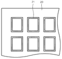
도 6은 도 2의 밀봉 부재에 글라스 프릿이 도포된 것을 도시하는 평면도이다.FIG. 6 is a plan view illustrating a glass frit coated on the sealing member of FIG. 2.
도 7은 도 1의 표시부의 일 부분을 개략적으로 도시하는 단면도이다.7 is a cross-sectional view schematically illustrating a part of the display unit of FIG. 1.
도 8 및 도 9는 본 발명의 일 실시예에 따른 방법으로 제조된 유기 발광 표시 장치의 평면 사진과 그 확대사진이다. 8 and 9 are planar photographs and enlarged photographs of organic light emitting display devices manufactured by a method according to an exemplary embodiment of the present invention.
도 10은 본 발명의 다른 실시예에 관한 유기 발광 표시 장치를 도시하는 개략적인 평면도이다.10 is a schematic plan view illustrating an organic light emitting display device according to another exemplary embodiment of the present invention.
도 11은 도 10에 도시한 유기 발광 표시 장치의 다른 변형예를 도시하는 개략적인 평면도이다.FIG. 11 is a schematic plan view illustrating another modified example of the organic light emitting diode display illustrated in FIG. 10.
<도면의 주요부분에 대한 부호의 간단한 설명><Brief description of symbols for the main parts of the drawings>
10: 기판 11: 표시부 10: substrate 11: display unit
20: 밀봉 부재 21: 글라스 프릿20: sealing member 21: glass frit
30: 스크린 마스크 31: 스크린부30: screen mask 31: screen part
32: 차폐부 37: 스퀴즈32: shield 37: squeeze
41: 버퍼층 42: 반도체층41: buffer layer 42: semiconductor layer
43: 게이트 절연막 44: 게이트 전극 43: gate insulating film 44: gate electrode
45: 층간 절연막 46: 소스 전극 45: interlayer insulating film 46: source electrode
47: 드레인 전극 48: 패시베이션막 47: drain electrode 48: passivation film
49: 화소 정의막 50: 유기 발광 소자 49: pixel defining layer 50: organic light emitting element
51: 제1 전극 52: 유기 발광층 51: first electrode 52: organic light emitting layer
53: 제2 전극 60: 실런트 53: second electrode 60: sealant
본 발명은 유기 발광 표시 장치 및 그 제조 방법에 관한 것으로 더 상세하게는 유기 발광 소자를 용이하게 밀봉할 수 있는 유기 발광 표시 장치 및 그 제조방법에 관한 것이다. The present invention relates to an organic light emitting display device and a method for manufacturing the same, and more particularly, to an organic light emitting display device and a method for manufacturing the organic light emitting device that can be easily sealed.
근래에 디스플레이 장치는 휴대가 가능한 박형의 평판 표시 장치로 대체되는 추세이다. 평판 디스플레이 장치 중에서도 전계 발광 표시장치는 자발광형 디스플 레이 장치로서 시야각이 넓고 콘트라스트가 우수할 뿐 만 아니라 응답속도가 빠르다는 장점을 가지고 있어서 차세대 디스플레이 장치로 주목 받고 있다. 또한 발광층의 형성 물질이 유기물로 구성되는 유기 발광 표시 장치는 무기 발광 표시 장치에 비해 휘도, 구동 전압 및 응답속도 특성이 우수하고 다색화가 가능하다는 점을 가지고 있다.Recently, display devices have been replaced by portable thin flat display devices. Among the flat panel display devices, the electroluminescent display device is a self-luminous display device, and has attracted attention as a next-generation display device because it has a wide viewing angle, excellent contrast, and fast response speed. In addition, an organic light emitting display device in which a light emitting layer is formed of an organic material has excellent luminance, driving voltage, and response speed, and may be multicolored, compared to an inorganic light emitting display device.
한편 유기 발광 표시 장치는 수분 침투에 의해 열화되는 특성을 가지고 있다. 그래서 수분 침투와 외부의 이물로부터 유기 발광 소자를 보호하기 위해 유기 발광 소자를 밀봉 하고 있다. 밀봉을 하기 위해 글라스 프릿을 사용하기도 한다. 그런데 글라스 프릿을 도포하는 데에는 많은 시간이 소요되고 정확한 패터닝이 힘든 문제점이 있다.On the other hand, the organic light emitting diode display has a property of deterioration due to moisture penetration. Therefore, the organic light emitting device is sealed in order to protect the organic light emitting device from moisture penetration and external foreign matter. Sometimes glass frit is used to seal. However, it takes a lot of time to apply the glass frit and there is a problem that accurate patterning is difficult.
본 발명은 유기 발광 소자를 용이하게 밀봉할 수 있는 유기 발광 표시 장치 및 그 제조 방법을 제공할 수 있다.The present invention can provide an organic light emitting display device and a method of manufacturing the same that can easily seal the organic light emitting device.
본 발명은 유기 발광 소자를 포함하는 표시부를 구비하는 기판을 준비하는 단계, 상기 기판의 일면에 대향하도록 밀봉 부재를 준비하는 단계, 상기 밀봉 부재의 일면에 상기 표시부의 외곽에 대응하도록 글라스 프릿을 도포하는 단계 및 상기 글라스 프릿을 매개로 상기 기판과 상기 밀봉 부재를 접합하는 단계를 포함하고, 상기 글라스 프릿을 도포하는 단계는 스크린 인쇄법을 이용하는 유기 발광 표시 장치의 제조 방법을 개시한다.The present invention provides a method of preparing a substrate including a display unit including an organic light emitting diode, preparing a sealing member to face one surface of the substrate, and coating a glass frit on one surface of the sealing member so as to correspond to an outer edge of the display unit. And bonding the substrate and the sealing member through the glass frit, and applying the glass frit discloses a method of manufacturing an organic light emitting display device using a screen printing method.
본 발명에 있어서 도포된 글라스 프릿을 소성하는 단계를 더 포함할 수 있다.In the present invention, the method may further include firing the coated glass frit.
본 발명에 있어서 상기 글라스 프릿을 소성하는 단계를 거친 후에 상기 글라스 프릿의 양면 중 상기 밀봉 부재를 향하는 일면의 폭에 대한 상기 글라스 프릿의 타면의 폭의 비가 0.5 내지 0.95를 만족할 수 있다.In the present invention, after the step of firing the glass frit, the ratio of the width of the other surface of the glass frit to the width of one surface of the both sides of the glass frit toward the sealing member may satisfy 0.5 to 0.95.
본 발명에 있어서 상기 글라스 프릿의 두께는 3 내지 100 마이크로 미터로 형성할 수 있다.In the present invention, the glass frit may have a thickness of 3 to 100 micrometers.
본 발명에 있어서 상기 글라스 프릿과 상기 표시부의 간격은 20 마이크로 미터 내지 20 밀리미터로 형성할 수 있다.In the present invention, the distance between the glass frit and the display unit may be 20 micrometers to 20 millimeters.
본 발명에 있어서 상기 글라스 프릿을 상기 밀봉 부재에 도포할 때 스크린 마스크를 이용하고, 상기 스크린 마스크는 200 내지 400 메쉬를 가질 수 있다.In the present invention, when applying the glass frit to the sealing member using a screen mask, the screen mask may have a 200 to 400 mesh.
본 발명에 있어서 상기 글라스 프릿에 의한 접합 단계는, 상기 글라스 프릿을 용융한 후 경화하는 단계를 포함할 수 있다.In the present invention, the bonding by the glass frit may include melting the glass frit and curing the glass frit.
본 발명에 있어서 상기 글라스 프릿을 용융하는 단계는 상기 글라스 프릿에 레이저를 조사하는 단계를 포함할 수 있다.In the present invention, melting the glass frit may include irradiating a laser to the glass frit.
본 발명에 있어서 상기 밀봉 부재상에 상기 글라스 프릿을 둘러싸도록 실런트를 도포하는 단계를 더 포함할 수 있다. The method may further include applying a sealant on the sealing member to surround the glass frit.
본 발명의 다른 측면에 따르면 기판, 상기 기판 상에 형성되고, 유기 발광 소자를 구비하는 표시부, 상기 유기 발광 소자를 밀봉하도록 상기 기판의 일면에 대향하여 접합되는 밀봉 부재 및 상기 표시부의 외곽에 대응하도록 상기 밀봉 부재 와 상기 기판 사이에 개재하는 글라스 프릿을 포함하고, 상기 글라스 프릿의 양면 중 상기 밀봉 부재를 향하는 일 면의 폭에 대한 상기 글라스 프릿의 타면의 폭의 비가 0.5 내지 1이고, 상기 글라스 프릿의 두께가 3 내지 100 마이크로 미터인 유기 발광 표시 장치를 개시한다.According to another aspect of the present invention, a substrate, a display unit formed on the substrate and including an organic light emitting element, a sealing member joined to one surface of the substrate to seal the organic light emitting element, and a shape corresponding to an outer portion of the display unit A glass frit interposed between the sealing member and the substrate, wherein the ratio of the width of the other surface of the glass frit to the width of one surface of the glass frit facing the sealing member is 0.5 to 1, and the glass frit An organic light emitting display device having a thickness of 3 to 100 micrometers is disclosed.
본 발명에 있어서 상기 밀봉 부재와 상기 기판 사이에 개재하는 실런트를 더 포함하고 상기 실런트는 상기 글라스 프릿을 둘러싸도록 상기 글라스 프릿의 외곽에 형성될 수 있다.In the present invention, the sealant may further include a sealant interposed between the sealing member and the substrate, and the sealant may be formed outside the glass frit to surround the glass frit.
이하 첨부된 도면들에 도시된 본 발명에 관한 실시예를 참조하여 본 발명의 구성 및 작용을 상세히 설명한다.Hereinafter, with reference to the embodiments of the present invention shown in the accompanying drawings will be described in detail the configuration and operation of the present invention.
도 1 내지 도 3은 본 발명의 일 실시예에 관한 유기 발광 표시 장치의 제조 방법을 순차적으로 도시한 개략적인 단면도이다.1 to 3 are schematic cross-sectional views sequentially illustrating a method of manufacturing an organic light emitting diode display according to an exemplary embodiment of the present invention.
도 1에 도시한 대로 기판(10)의 일면에 복수개의 표시부(11)를 형성한다.As shown in FIG. 1, a plurality of
기판(10)은 SiO2를 주성분으로 하는 투명한 유리 재질로 이루어질 수 있다. 비록 도시하지 않았으나 기판(10)의 상면에는 기판(10)의 평활성과 불순 원소의 침투를 차단하기 위하여 버퍼층(미도시)을 더 포함할 수 있고, 버퍼층은 SiO2 및/또는 SiNx 등으로 형성할 수 있다. 기판(10)은 반드시 이에 한정되는 것은 아니며 투명한 플라스틱 재로 형성할 수도 있고, 금속 호일 등도 적용이 가능하다.The
표시부(11)는 화상을 구현하는 유기 발광 소자를 포함하고 있다. 유기 발광 소자는 능동형 소자일수도 있고 수동형 소자일수도 있다. 이에 대한 상세한 설명은 후술한다.The
도 2를 참조하면 기판(10)의 일 면에 대향하도록 밀봉 부재(20)를 준비한다. 밀봉 부재(20)에는 기판(10)의 표시부(11)의 외곽에 대응하도록 글라스 프릿(21)이 형성된다.Referring to FIG. 2, the sealing
밀봉 부재(20)는 외부의 수분이나 산소 등으로부터 유기 발광 소자를 보호하기 위해 형성하는 것으로 밀봉 부재(20)는 투명한 재질로 형성된다. 이를 위해 글라스, 플라스틱 또는 유기물과 무기물의 복수의 중첩된 구조일 수도 있다. The sealing
밀봉 부재(20)에 글라스 프릿(21)을 형성하고 도 3에 도시한 것과 같이 기판(10)과 밀봉 부재(20)를 결합한다. A glass frit 21 is formed on the sealing
밀봉 부재(20)에 글라스 프릿(21)을 형성하는 방법을 상세히 설명하기로 한다. 도 4는 도 2의 글라스 프릿을 스크린 인쇄법을 이용하여 밀봉 부재에 형성하는 단계를 개략적으로 도시하는 단면도이다. A method of forming the glass frit 21 on the sealing
본 발명에서는 스크린 인쇄법을 이용하여 글라스 프릿(21)을 밀봉 부재(20)에 형성한다. 스크린 인쇄법을 이용하는 경우 원하는 패턴으로 막을 형성하기 위해 스크린 마스크를 필요로 한다.In the present invention, the glass frit 21 is formed on the sealing
스크린 마스크(30)는 도 4에 도시한 것과 같이 글라스 프릿(21)이 스며드는 스크린부(31), 스크린부(31)를 한정하는 차폐부(32)를 포함한다.The
스크린 마스크(30)는 소정 입도의 글라스 프릿 페이스트가 스며들 수 있도록 나일론 천과 같은 메쉬형의 부재로 형성되는 데, 스크린부(31)의 영역을 제외한 영역에 대해 경화제를 이용해 상기 천의 구멍을 막아 차폐부(32)를 형성하고, 차폐 부(32)에 따라 스크린부(31)의 패턴을 한정한다. 이러한 스크린 인쇄용 마스크(30)로는 이 외에도 폴리 에스테르 소재, 스텐레스강으로 만들어진 메쉬가 사용될 수 있다. 메쉬의 범위는 다양할 수 있으나 글라스 프릿(21)의 밀봉 특성상 200 내지 400 메쉬를 가지는 스크린 마스크(30)를 사용하는 것이 바람직하다. 이는 글라스 프릿 페이스트의 입도 및 점도를 고려한 것이다.The
스크린 마스크(30)의 하면, 예컨대 차폐부(32)에 대응되는 영역의 하면에는 도 4에서 볼 수 있듯이 지지 부재(33)가 접합된다. 지지 부재(33)는 레진(resin)과 같은 유제가 사용될 수 있으나, 반드시 이에 한정되는 것은 아니며, 스크린 인쇄용 마스크(30)를 지지해줄 수 있는 것이면 어떠한 것이든 무방하다. 지지 부재(33)는 패턴의 정밀도를 높이기 위해 도 4에서 볼 수 있듯이, 차폐부(32)보다 약간 정도 넓게 스크린부(31)를 둘러쌀 수 있다.The
스크린 마스크(30) 상에 글라스 프릿 페이스트를 도포한 후, 스크린부(31)에 대응되는 영역을 스퀴즈(37)로 눌러, 스크린부(31)의 메쉬를 통해 글라스 프릿 페이스트가 배출되어 밀봉 부재(20)상에 소정 패턴 막으로 된 글라스 프릿(21)을 형성한다.After applying the glass frit paste on the
1장의 기판(10)으로 복수개의 유기 발광 표시 장치를 만들기 위해 1장의 기판(20)에는 독립된 복수개의 표시부(11)가 형성된다. 그리고 각 표시부(11)의 외곽에 글라스 프릿(21)을 형성할 수 있도록 스크린 마스크(30)는 복수의 스크린부(31)를 포함한다.In order to make a plurality of organic light emitting display devices using one
스크린 마스크(30)를 밀봉 부재(20)에 밀착시킨 후 스크린 인쇄를 하게 된 다. 이 때 스크린부(31)와 밀봉 부재(20)사이의 압력이 전체 스크린부(31)에 있어 균일해야 전체적으로 균일한 도포가 가능하다. 글라스 프릿(21)을 스크린 인쇄한 후에는 소정의 소성 공정을 거쳐 글라스 프릿(21)을 경화할 수 있다.The
도 5는 본 발명의 일 실시예에 관한 글라스 프릿의 상세한 배치 위치 및 구조를 도시하는 단면도이다. 글라스 프릿(21)은 밀봉 부재(20)상에 상, 하면의 폭이 다르게 형성될 수 있다. 즉 도 5에 도시된 것과 같이 글라스 프릿(21)의 양면 중 밀봉 부재(20)를 향하는 일면의 폭(w1)이 타면의 폭(w2)보다 크다. 바람직하게는, w2/w1는 0.5 내지 0.95이다. w2/w1 값이 작으면 즉 w2 값이 지나치게 작아지면 글라스 프릿(21)과 기판(10)과의 접촉면적이 줄어들어 밀봉능력이 감소한다.5 is a cross-sectional view showing the detailed arrangement position and structure of the glass frit according to one embodiment of the present invention. The
디스펜스법으로 글라스 프릿(21)을 형성하는 경우에는 디스펜서의 노즐에서 프릿 페이스트가 자연스럽게 분출되므로 글라스 프릿(21)이 형성된 후에 글라스 프릿(21)의 상면이 균일하지 않다. 또한 노즐에서 분출되는 프릿 페이스트의 특성상 프릿 페이스트가 밀봉 부재(20)와 닿는 부분이 자연스럽게 늘어난다. 결과적으로 소성후 글라스 프릿(21)의 w2/w1의 비가 낮아지게 된다.When the
그러나 스크린 인쇄법으로 글라스 프릿(21)을 형성하는 경우에는 스크린 마스크(30)를 이용한다. 스크린 마스크(30)의 스크린부(31)로 프릿 페이스트가 스며들도록 스퀴즈(37)로 누르게 된다. 즉 스퀴즈(37)로 프릿 페이스트의 상면을 누르게 되므로 밀봉 부재(20)상에 글라스 프릿(21)이 형성되었을 때에 상면 즉 밀봉 부재(20)와 접하지 않는 글라스 프릿(21)의 면이 매끄럽게 되고 상, 하변의 폭의 비 즉 w2/w1값도 1에 가까운 높은 값을 가질 수 있다. 특히 스크린 인쇄법을 이용할 경우에는 별도의 공정없이도 w2/w1의 값이 0.7이상의 값을 용이하게 얻을 수 있다.However, when the
글라스 프릿(21)의 두께(h)는 3 내지 100 마이크로 미터로 형성할 수 있다. 기판(10)에 형성되는 표시부(11)의 두께를 확보할 수 있도록 글라스 프릿(21)은 3 마이크로 미터 이상의 두께로 형성될 수 있다. 또한 글라스 프릿(21)이 지나치게 두꺼우면 빛이 산란되어 화질 특성이 감소하므로 100마이크로 미터 이하의 두께를 갖도록 형성하는 것이 바람직하다.The thickness h of the
글라스 프릿(21)과 표시부(11)는 20 마이크로 미터 이상의 간격을 가지도록 형성될 수 있다. 글라스 프릿(21)과 표시부(11)의 간격(d)이 너무 좁으면 후속 공정인 레이저 경화 공정 시에 표시부(11)가 손상을 받을 염려가 있다. 그러므로 글라스 프릿(21)과 표시부(11)와의 간격(d)은 20 마이크로 미터 이상이 되는 것이 바람직하다. 그러나 그 간격(d)이 너무 넓으면 기판(10)에서의 데드 스페이스가 늘어나게 된다. 그러므로 공정 조건 및 제조하려는 유기 발광 표시 장치의 크기를 고려해 글라스 프릿(21)과 표시부(11)와의 간격(d)을 적절하게 결정할 수 있는데 20 밀리미터로 이하로 형성할 수 있다. The
도 6은 도 2의 밀봉 부재에 글라스 프릿이 도포된 것을 도시하는 평면도이다. 전술한 바와 같이 글라스 프릿(21)은 각 표시부(11)의 외곽에 대응되도록 도포된다.FIG. 6 is a plan view illustrating a glass frit coated on the sealing member of FIG. 2. As described above, the
밀봉 부재(20)상에 글라스 프릿(21)을 형성한 후에 밀봉 부재(20)와 기판(10)을 접합한다. 먼저 기판(10)상에 밀봉 기판(20)을 배치한다. 이때 밀봉 기판(20)상에 형성된 글라스 프릿(21)이 표시부(11)의 외곽에 대응되도록 정확히 얼 라인 한다. 정확히 얼라인을 한 후에 글라스 프릿(21)을 용융하는 공정을 거친다. 다양한 방법을 이용하여 글라스 프릿(21)을 용융할 수 있으나 표시부(11)에 미치는 열적 손상을 방지하기 위해서는 레이저를 이용하여 글라스 프릿(21)을 용융하는 것이 바람직하다. 용융된 글라스 프릿(21)이 냉각되면 기판(10)과 밀봉 부재(20)는 글라스 프릿(21)에 의해 접합될 수 있다. 특히 레이저를 이용해 글라스 프릿(21)을 용융할 경우에 글라스 프릿(21)의 상면 즉 밀봉 부재(20)와 접하지 않는 면을 조사할 수 있다. 이 경우 글라스 프릿(21)의 상면이 용융되어 소성후 보다 상면의 폭(w2)을 크게 할 수 있다. 그래서 소성전인 글라스 프릿(21)의 w2/w1의 값의 범위는 0.5 내지 0.95 였으나 레이저 조사후에는 0.5 내지 1의 값을 가지도록 할 수 있다.After the
디스펜스법을 사용하여 프릿을 형성할 경우엔 디스펜서의 특성상 프릿의 도포 면의 폭이 일정하지 않다. 나아가 프릿을 도포하는 시작점과 끝점에서는 프릿의 폭이 굵어지거나 얇아지게 된다. 그 결과 레이저를 조사할 경우 프릿 도포 면의 폭이 일정하지 않은 부분에 응력이 집중되어 밀봉을 파괴시킬 수 있다. 그러나 전술한 대로 스크린 인쇄법으로 프릿(21)을 도포하면 도 6에 도시한 것과 같이 프릿(21)의 도포 면이 고르게 형성되어 프릿(21)의 신뢰성이 향상되고 그 결과 유기 발광 표시 장치의 밀봉 능력도 개선된다.When the frit is formed using the dispense method, the width of the coated surface of the frit is not constant due to the characteristics of the dispenser. Furthermore, the frit becomes thicker or thinner at the start and end points of applying the frit. As a result, when the laser is irradiated, the stress can be concentrated in the portion where the width of the frit coating surface is not constant, which can break the seal. However, when the frit 21 is coated by the screen printing method as described above, as shown in FIG. 6, the application surface of the frit 21 is evenly formed, thereby improving the reliability of the frit 21 and consequently sealing the organic light emitting display device. The ability is also improved.
기판(10)과 밀봉 부재(20)를 접합한 후에 각 표시부(11)주변에 형성된 글라스 프릿(21)의 외곽을 스크라이빙하여 복수 개의 유기 발광 표시 장치를 제조할 수 있다.After the
본 발명의 일 실시예에 관한 유기 발광 표시 장치의 제조 방법은 다양한 형태의 유기 발광 표시 장치를 제조하는데 모두 적용이 가능하다. 도 7은 도 1의 표시부의 일부를 개략적으로 도시하는 단면도로서 능동(active matrix type:AM) 구동형 유기 발광 소자를 포함한 유기 발광 표시 장치의 부분 단면도이다. The manufacturing method of the organic light emitting diode display according to the exemplary embodiment of the present invention may be applied to manufacturing various types of organic light emitting diode display devices. FIG. 7 is a cross-sectional view schematically illustrating a portion of the display unit of FIG. 1, and is a partial cross-sectional view of an organic light emitting diode display including an active matrix type (AM) driven organic light emitting diode.
기판(10)의 상면에 기판(10)의 평활성과 불순 원소의 침투를 차단하기 위하여 버퍼층(41)을 형성할 수 있다. 버퍼층(21)은 SiO2 및/또는 SiNx 등으로 형성할 수 있다. The
기판(10)의 상면에 박막 트랜지스터(TFT)가 형성되어 있다. 이 박막 트랜지스터(TFT)는 각 화소별로 적어도 하나씩 형성되는 데, 유기 발광 소자(50)에 전기적으로 연결된다.The thin film transistor TFT is formed on the upper surface of the
구체적으로 버퍼층(41)상에 소정 패턴의 반도체층(42)이 형성된다. 반도체층(42)은 아모퍼스 실리콘 또는 폴리 실리콘과 같은 무기 반도체나 유기 반도체로 형성될 수 있고 소스 영역, 드레인 영역 및 채널 영역을 포함한다.Specifically, the
반도체층(42)의 상부에는 SiO2, SiNx 등으로 형성되는 게이트 절연막(43)이 형성되고, 게이트 절연막(43)상부의 소정 영역에는 게이트 전극(44)이 형성된다. 게이트 전극(44)은 MoW, Al/Cu 등과 같은 물질로 형성하나 이에 한정되지 않고 인접층과의 밀착성, 적층되는 층의 평탄성, 전기 저항 및 가공성등을 고려하여 다양한 재료를 사용할 수 있다. A
게이트 전극(44)은 TFT 온/오프 신호를 인가하는 게이트 라인(미도시)과 연 결되어 있다.The
게이트 전극(14)의 상부로는 층간 절연막(45)을 형성하고, 컨택홀을 통해 소스 전극(46) 및 드레인 전극(47)이 각각 반도체층(42)의 소스 및 드레인 영역에 접하도록 형성한다. 이렇게 형성한 TFT는 패시베이션막(48)을 덮어 보호한다. An interlayer insulating
패시베이션막(48)은 무기 절연막 및/또는 유기 절연막을 사용하여 형성할 수 있는데 무기 절연막으로는 SiO2, SiNx, SiON, Al2O3, TiO2, Ta2O5, HfO2, ZrO2, BST, PZT 등이 포함되도록 할 수 있고, 유기 절연막으로는 일반 범용고분자(PMMA, PS), phenol그룹을 갖는 고분자 유도체, 아크릴계 고분자, 이미드계 고분자, 아릴에테르계 고분자, 아마이드계 고분자, 불소계고분자, p-자일렌계 고분자, 비닐알콜계 고분자 및 이들의 블렌드 등이 포함되도록 할 수 있다. 패시베이션막(48)은 무기 절연막과 유기 절연막의 복합 적층체로도 형성할 수 있다.The
패시베이션막(48) 상부에는 유기 발광 소자의 애노우드 전극이 되는 제1 전극(51)을 형성하고, 이를 덮도록 절연물로 화소 정의막(49)(pixel define layer)을 형성한다. 이 화소 정의막(49)에 소정의 개구를 형성한 후, 이 개구로 한정된 영역 내에 유기 발광 소자의 유기 발광층(52)을 형성한다. 그리고, 전체 화소들을 모두 덮도록 유기 발광 소자의 캐소오드 전극이 되는 제2 전극(53)을 형성된다. 물론 제1 전극(51)과 제2 전극(53)의 극성은 서로 반대로 바뀌어도 무방하다.A
유기 발광 소자는 전류의 흐름에 따라 빛을 발광하여 화상을 표시하는 것으로 TFT의 드레인 전극(47)에 콘택홀을 통하여 전기적으로 연결된 제1 전극(51), 유 기 발광층(52) 및 제2 전극(53)을 포함한다. The organic light emitting element emits light according to the flow of current to display an image. The organic light emitting element is a
제1 전극(51)은 포토 리소그래피법에 의해 화소에 대응하는 형태로 형성할 수 있다.제1 전극(51)의 상부로 제2 전극(53)을 배치하는데 외부단자(미도시)에 연결하여 캐소오드(cathode)전극으로 작용할 수 있다. 제2 전극(53)은 화상이 구현되는 액티브 영역 전체에 걸쳐 형성할 수 있다. 제1 전극(51)의 극성과 제2 전극(53)의 극성은 서로 반대가 되어도 무방하다. 기판(10)의 방향으로 화상이 구현되는 배면 발광형(bottom emission type)일 경우, 제1 전극(51)은 투명 전극이 되고, 제2 전극(53)은 반사전극이 될 수 있다. 제1 전극(51)은 일함수가 높은 ITO, IZO, ZnO, 또는 In2O3 등으로 형성하고, 제2 전극(53)은 일함수가 작은 금속 즉, Ag, Mg, Al, Pt, Pd, Au, Ni, Nd, Ir, Cr, Li, Ca 등으로 형성할 수 있다.The
도 1에 도시한 것과 같이 제2 전극(53)의 방향으로 화상을 구현하는 전면 발광형(top emission type)일 경우, 제1 전극(51)은 반사 전극으로 구비될 수 있고, 제2 전극(53)은 투명 전극으로 구비될 수 있다. 이 때, 제1 전극(51)이 되는 반사 전극은 Ag, Mg, Al, Pt, Pd, Au, Ni, Nd, Ir, Cr, Li, Ca 및 이들의 화합물 등으로 반사막을 형성한 후, 그 위에 일함수가 높은 ITO, IZO, ZnO, 또는 In2O3 등을 형성하여 이루어질 수 있다. 그리고, 제2 전극(53)이 되는 투명 전극은, 일함수가 작은 금속 즉, Ag, Mg, Al, Pt, Pd, Au, Ni, Nd, Ir, Cr, Li, Ca 및 이들의 화합물을 증착한 후, 그 위에 ITO, IZO, ZnO, 또는 In2O3 등의 투명 도전물질로 보조 전극층이나 버스 전극 라인을 형성할 수 있다.As shown in FIG. 1, in the case of a top emission type that implements an image in the direction of the
양면 발광형의 경우, 제1 전극(51)과 제2 전극(53) 모두를 투명 전극으로 형 성할 수 있다.In the case of the double-sided light emission type, both the
제1 전극(51)과 제2 전극(53)의 사이에 개재된 유기 발광층(52)은 제1 전극(51)과 제2 전극(53)의 전기적 구동에 의해 발광한다. 유기 발광층(52)은 저분자 또는 고분자 유기물을 사용할 수 있다. 유기 발광층(52)이 저분자 유기물로 형성되는 경우 유기 발광층(52)을 중심으로 제1 전극(51)의 방향으로 홀 수송층 및 홀 주입층 등이 적층되고, 제2 전극(53) 방향으로 전자 수송층 및 전자 주입층 등이 적층된다. 이외에도 필요에 따라 다양한 층들이 적층될 수 있다. 사용 가능한 유기 재료도 구리 프탈로시아닌(CuPc: copper phthalocyanine), N,N-디(나프탈렌-1-일)-N,N'-디페닐-벤지딘 (N,N'-Di(naphthalene-1-yl)-N,N'-diphenyl-benzidine: NPB) , 트리스-8-하이드록시퀴놀린 알루미늄(tris-8-hydroxyquinoline aluminum)(Alq3) 등을 비롯해 다양하게 적용 가능하다. The organic
한편, 고분자 유기물로 형성된 고분자 유기층의 경우에는 유기 발광층(52)을 중심으로 제1 전극(51)의 방향으로 홀 수송층(Hole Transport Layer: HTL)만이 포함될 수 있다. 상기 고분자 홀 수송층은 폴리에틸렌 디히드록시티오펜 (PEDOT: poly-(2,4)-ethylene-dihydroxy thiophene)이나, 폴리아닐린(PANI: polyaniline) 등을 사용하여 잉크젯 프린팅이나 스핀 코팅의 방법에 의해 제1 전극(51) 상부에 형성되며, 고분자 유기 발광층(52)은 PPV, Soluble PPV's, Cyano-PPV, 폴리플루오렌(Polyfluorene) 등을 사용할 수 있으며 잉크젯 프린팅이나 스핀 코팅 또는 레이저를 이용한 열전사방식 등의 통상의 방법으로 컬러 패턴을 형성할 수 있다.Meanwhile, in the case of the polymer organic layer formed of the polymer organic material, only the hole transport layer (HTL) may be included in the direction of the
이상 도 7에 도시한 탑게이트 구조의 능동형 유기 발광 표시 장치만을 설명 하였으나 전술한 바와 같이 본 발명은 이에 한정되지 않고 기타 다양한 형태의 유기 발광 표시 장치에 적용이 가능하다. As described above, only the active organic light emitting display device having the top gate structure illustrated in FIG. 7 is described. However, the present invention is not limited thereto, and the present invention can be applied to other organic light emitting display devices.
본 발명의 일 실시예에 관한 유기 발광 표시 장치의 제조 방법을 이용하면 스크린 인쇄법을 이용해 글라스 프릿(21)을 도포하게 되므로 디스펜스법등에 비해 공정 시간이 매우 단축된다. 그리고 스크린 인쇄법을 이용하면 글라스 프릿(21)의 패터닝이 용이하고 단면의 모양을 균일하게 형성할 수 있다. 또한 글라스 프릿(21)의 우수한 밀봉 특성으로 외부의 수분이나 이물로부터 유기 발광 소자를 용이하게 보호할 수 있다.When the method of manufacturing the organic light emitting diode display according to the exemplary embodiment of the present invention is used, the
도 8 및 도 9는 본 발명의 일 실시예에 관한 방법으로 제조된 유기 발광 표시 장치의 평면 사진과 그 확대사진이다. 8 and 9 are planar photographs and enlarged photographs of organic light emitting display devices manufactured by a method according to an exemplary embodiment of the present invention.
실험을 위해 325메쉬의 스크린 마스크(30)를 사용하여 글라스 프릿(21)을 밀봉 부재(20)에 도포하고, 420℃에서 10분간 소성하였다. 그리고 밀봉 기판(20)을 표시부(11)가 형성된 기판(10)과 얼라인 한 후에 레이저를 조사하여 기판(10)과 밀봉 부재(20)를 합착하였다. 도 8의 A의 확대도인 도 9를 참조하면 글라스 프릿(21)이 형성된 패턴이 직선으로 형성되어 있어 원하는 글라스 프릿(21)의 패터닝이 용이하게 됨을 알 수 있다. 또한 글라스 프릿(21)의 형성된 폭이 충분히 확보되어 있어 기판(10)과 밀봉 부재(20)의 접착의 신뢰성을 높일 수 있다. 또한 스크린 인쇄법으로 글라스 프릿(21)을 도포하는 경우 스크린 마스크(30)의 메쉬형상이 글라스 프릿(21)에 남을 수 있는데 도 9는 글라스 프릿(21)상에 스크린 마스크(30)의 메쉬의 흔적이 남지 않은 것을 보여준다. For the experiment, the
도 10은 본 발명의 다른 실시예에 관한 유기 발광 표시 장치를 도시하는 개략적인 평면도이다. 이하에서는 전술한 실시예와 상이한 점을 중심으로 설명한다. 동일한 참조부호는 동일한 부재를 나타낸다.10 is a schematic plan view illustrating an organic light emitting display device according to another exemplary embodiment of the present invention. The following description will focus on differences from the above-described embodiment. Like reference numerals denote like elements.
본 실시예에 관한 유기 발광 표시 장치의 제조 방법은 실런트(60)를 밀봉부재에 도포하는 단계를 더 포함한다. 실런트(60)는 글라스 프릿(21)들을 둘러싸도록 도포한다. 실런트(60)는 자외선 경화 실런트 기타 다양한 종류의 재질이 사용 가능하다. The manufacturing method of the organic light emitting diode display according to the present embodiment further includes applying the
도 11은 도 10에 도시한 유기 발광 표시 장치의 다른 변형예를 도시한 평면도이다. 도 10과 달리 실런트(60)는 글라스 프릿(21)을 둘러싸되, 각각의 표시부(11)를 밀봉하는 글라스 프릿(21)을 둘러싸도록 형성된다. FIG. 11 is a plan view illustrating another modified example of the organic light emitting diode display illustrated in FIG. 10. Unlike FIG. 10, the
도 10과 도 11의 경우 실런트(60)에 의해 1차적으로 밀봉이 되고 글라스 프릿(21)으로 다시 한번 밀봉이 되는 구조이다. 그래서 밀봉 효과를 향상시킬 수 있다. 특히 도 11은 각 표시부(11)별로 스크라이빙을 하여도 2중으로 밀봉된 상태의 압력을 유지할 수 있다. 10 and 11, the
본 발명에 관한 유기 발광 표시 장치 및 그 제조 방법은 유기 발광 소자를 용이하게 밀봉할 수 있다.The organic light emitting diode display and the manufacturing method thereof according to the present invention can easily seal the organic light emitting element.
도면에 도시된 실시예를 참고로 설명되었으나 이는 예시적인 것에 불과하며, 본 기술 분야의 통상의 지식을 가진 자라면 이로부터 다양한 변형 및 균등한 다른 실시예가 가능하다는 점을 이해할 것이다. 따라서, 본 발명의 진정한 기술적 보호 범위는 첨부된 특허청구범위의 기술적 사상에 의하여 정해져야 할 것이다.Although described with reference to the embodiment shown in the drawings it is merely exemplary, those skilled in the art will understand that various modifications and equivalent other embodiments are possible from this. Therefore, the true technical protection scope of the present invention will be defined by the technical spirit of the appended claims.
Claims (12)
Priority Applications (6)
| Application Number | Priority Date | Filing Date | Title |
|---|---|---|---|
| KR1020060123372A KR20080051756A (en) | 2006-12-06 | 2006-12-06 | OLED display and manufacturing method thereof |
| JP2007071107A JP4612009B2 (en) | 2006-12-06 | 2007-03-19 | Organic light-emitting display device and method for manufacturing the same |
| US11/754,938 US7841919B2 (en) | 2006-12-06 | 2007-05-29 | Method of sealing an organic light emitting display using closed loop pattern of frit paste composition |
| TW096120065A TWI376981B (en) | 2006-12-06 | 2007-06-05 | Organic light emitting display apparatus and method of manufacturing the same |
| CN2007101468199A CN101198201B (en) | 2006-12-06 | 2007-08-24 | Organic light emitting display apparatus and method of manufacturing the same |
| EP07115069.2A EP1930967B1 (en) | 2006-12-06 | 2007-08-28 | Method of making an organic light emitting display apparatus and apparatus therefor |
Applications Claiming Priority (1)
| Application Number | Priority Date | Filing Date | Title |
|---|---|---|---|
| KR1020060123372A KR20080051756A (en) | 2006-12-06 | 2006-12-06 | OLED display and manufacturing method thereof |
Publications (1)
| Publication Number | Publication Date |
|---|---|
| KR20080051756A true KR20080051756A (en) | 2008-06-11 |
Family
ID=38711077
Family Applications (1)
| Application Number | Title | Priority Date | Filing Date |
|---|---|---|---|
| KR1020060123372A Ceased KR20080051756A (en) | 2006-12-06 | 2006-12-06 | OLED display and manufacturing method thereof |
Country Status (6)
| Country | Link |
|---|---|
| US (1) | US7841919B2 (en) |
| EP (1) | EP1930967B1 (en) |
| JP (1) | JP4612009B2 (en) |
| KR (1) | KR20080051756A (en) |
| CN (1) | CN101198201B (en) |
| TW (1) | TWI376981B (en) |
Cited By (2)
| Publication number | Priority date | Publication date | Assignee | Title |
|---|---|---|---|---|
| WO2011016650A3 (en) * | 2009-08-03 | 2011-04-28 | 주식회사 동진쎄미켐 | Method and apparatus for packaging a light-transmitting unit for an optical element |
| KR101256026B1 (en) * | 2009-11-24 | 2013-04-18 | 삼성디스플레이 주식회사 | Organic light emitting diode display |
Families Citing this family (37)
| Publication number | Priority date | Publication date | Assignee | Title |
|---|---|---|---|---|
| US8716850B2 (en) * | 2007-05-18 | 2014-05-06 | Semiconductor Energy Laboratory Co., Ltd. | Semiconductor device and method for manufacturing the same |
| KR101375334B1 (en) * | 2008-07-17 | 2014-03-20 | 삼성디스플레이 주식회사 | Organic light emitting display apparatus and method of manufacturing thereof |
| KR101100943B1 (en) * | 2008-10-31 | 2011-12-29 | 삼성모바일디스플레이주식회사 | Manufacturing method of organic light emitting display device |
| US8860305B2 (en) | 2009-07-09 | 2014-10-14 | Corning Incorporated | Methods for forming fritted cover sheets with masks and glass packages comprising the same |
| US20110014731A1 (en) * | 2009-07-15 | 2011-01-20 | Kelvin Nguyen | Method for sealing a photonic device |
| KR101022141B1 (en) * | 2009-10-27 | 2011-03-17 | 삼성모바일디스플레이주식회사 | An organic light emitting display device comprising a thin film transistor, a method of manufacturing the same, and a thin film transistor |
| KR101137394B1 (en) * | 2010-07-05 | 2012-04-20 | 삼성모바일디스플레이주식회사 | Laser beam irradiation apparatus and substrate sealing apparatus comprising the same |
| KR20120019017A (en) * | 2010-08-24 | 2012-03-06 | 삼성모바일디스플레이주식회사 | Organic electroluminescence emitting display device and manufacturing method of the same |
| JP2012186080A (en) * | 2011-03-07 | 2012-09-27 | Panasonic Corp | Planar light emitting device and method for manufacturing the same |
| TW202414842A (en) | 2011-05-05 | 2024-04-01 | 日商半導體能源研究所股份有限公司 | Semiconductor device and method for manufacturing the same |
| JP6111022B2 (en) * | 2011-06-17 | 2017-04-05 | 株式会社半導体エネルギー研究所 | Method for manufacturing sealing body and method for manufacturing light-emitting device |
| JP5816029B2 (en) | 2011-08-24 | 2015-11-17 | 株式会社半導体エネルギー研究所 | Light emitting device |
| TWI569490B (en) | 2011-11-28 | 2017-02-01 | 半導體能源研究所股份有限公司 | Sealing body, light emitting module, and method of manufacturing the same |
| KR20130060131A (en) * | 2011-11-29 | 2013-06-07 | 가부시키가이샤 한도오따이 에네루기 켄큐쇼 | Sealed structure, light-emitting device, electronic device, and lighting device |
| TW201707202A (en) | 2011-11-29 | 2017-02-16 | 半導體能源研究所股份有限公司 | Sealing structure, illuminating device, electronic device, and lighting device |
| KR102001815B1 (en) | 2011-11-29 | 2019-07-19 | 가부시키가이샤 한도오따이 에네루기 켄큐쇼 | Method of manufacturing sealed body and method of manufacturing light-emitting device |
| US9012927B2 (en) * | 2011-11-30 | 2015-04-21 | Canon Kabushiki Kaisha | Display device |
| KR101333138B1 (en) | 2012-03-05 | 2013-11-26 | 삼성디스플레이 주식회사 | Method for preparing organic light emitting device, substrate for transiting of an inorganic film and organic light emitting device |
| KR101991863B1 (en) * | 2012-08-28 | 2019-06-24 | 삼성디스플레이 주식회사 | Encapsulation sheet, manufacturing method of organic light emitting display device comprising the same and organic light emitting display device |
| JP6019997B2 (en) * | 2012-09-26 | 2016-11-02 | ソニー株式会社 | Display device and electronic device |
| CN103000251B (en) * | 2012-11-10 | 2015-05-20 | 江苏瑞德新能源科技有限公司 | Solar cell silver-backed slurry with wide sintering process window |
| CN103367658B (en) * | 2013-07-17 | 2016-08-31 | 深圳市华星光电技术有限公司 | A kind of glass package structure and method for packing |
| CN104576744A (en) * | 2013-10-24 | 2015-04-29 | 中国科学院苏州纳米技术与纳米仿生研究所 | Carbon nanotube thin-film transistor, AMOLED (active matrix organic light emitting diode) pixel flexible driving circuit and manufacturing method thereof |
| CN103972268B (en) * | 2014-04-22 | 2017-01-04 | 京东方科技集团股份有限公司 | Organic LED display panel and preparation method thereof |
| US20150372251A1 (en) * | 2014-06-19 | 2015-12-24 | Toshishige Fujii | Electric element package |
| KR102223679B1 (en) * | 2014-08-04 | 2021-03-08 | 삼성디스플레이 주식회사 | Display panel and mother panel for manufacturing the display panel |
| US9698376B2 (en) * | 2014-10-24 | 2017-07-04 | Shenzhen China Star Optoelectronics Technology Co., Ltd | Packaging method and packaging structure of substrate |
| CN104409662B (en) | 2014-11-10 | 2017-07-18 | 京东方科技集团股份有限公司 | Oled panel and preparation method, screen printing plate, display device |
| EP3236249B1 (en) * | 2014-12-15 | 2024-03-13 | Joint Stock Company "Akme-Engineering" | Sensor for sensing hydrogen in liquid and gaseous media |
| KR102221554B1 (en) * | 2015-01-19 | 2021-03-02 | 삼성디스플레이 주식회사 | Display device |
| CN104867962B (en) * | 2015-05-06 | 2019-04-05 | 京东方科技集团股份有限公司 | An OLED array substrate and its manufacturing method, and an OLED display device |
| CN105058957B (en) * | 2015-07-27 | 2018-12-28 | 京东方科技集团股份有限公司 | Halftone and preparation method thereof, packaging method, display panel, display device |
| KR102382487B1 (en) * | 2017-09-15 | 2022-04-01 | 엘지디스플레이 주식회사 | Organic light emitting display device |
| CN107742472B (en) * | 2017-09-25 | 2021-03-26 | 昆山国显光电有限公司 | Packaging mask plate, packaging method and display panel |
| FR3118461B1 (en) * | 2020-12-24 | 2024-01-19 | Saint Gobain | METHOD FOR MANUFACTURING GREENHOUSE GLAZING AND SUCH GREENHOUSE GLAZING |
| CN114039019B (en) * | 2021-11-08 | 2025-04-04 | 福建华佳彩有限公司 | A Frit packaging method and device |
| CN118023078B (en) * | 2024-02-23 | 2024-08-09 | 沃卡姆(山东)真空玻璃科技有限公司 | Curved surface vacuum glass powder coating thickness monitoring device |
Family Cites Families (12)
| Publication number | Priority date | Publication date | Assignee | Title |
|---|---|---|---|---|
| JPS526097B2 (en) * | 1972-03-14 | 1977-02-18 | ||
| JPH053006A (en) | 1991-06-25 | 1993-01-08 | Mitsubishi Electric Corp | Light emitting element |
| CN2384314Y (en) * | 1999-07-15 | 2000-06-21 | 张志林 | Organic film electroluminescent element with multi-layer seal |
| US6555025B1 (en) * | 2000-01-31 | 2003-04-29 | Candescent Technologies Corporation | Tuned sealing material for sealing of a flat panel display |
| JP2005510831A (en) | 2001-05-24 | 2005-04-21 | オリオン エレクトリック カンパニー,リミテッド | Container for encapsulation of organic light-emitting diode and method for manufacturing the same |
| TW517356B (en) * | 2001-10-09 | 2003-01-11 | Delta Optoelectronics Inc | Package structure of display device and its packaging method |
| DE10219951A1 (en) * | 2002-05-03 | 2003-11-13 | Patent Treuhand Ges Fuer Elektrische Gluehlampen Mbh | Process for encapsulating a component based on organic semiconductors |
| JP4299021B2 (en) * | 2003-02-19 | 2009-07-22 | ヤマト電子株式会社 | Sealing material and sealing paste |
| US6998776B2 (en) * | 2003-04-16 | 2006-02-14 | Corning Incorporated | Glass package that is hermetically sealed with a frit and method of fabrication |
| WO2005050751A2 (en) | 2003-11-12 | 2005-06-02 | E.I. Dupont De Nemours And Company | Encapsulation assembly for electronic devices |
| US7371143B2 (en) * | 2004-10-20 | 2008-05-13 | Corning Incorporated | Optimization of parameters for sealing organic emitting light diode (OLED) displays |
| JP2006228647A (en) * | 2005-02-21 | 2006-08-31 | Idemitsu Kosan Co Ltd | Organic electroluminescent sealing substrate and method for manufacturing the same |
-
2006
- 2006-12-06 KR KR1020060123372A patent/KR20080051756A/en not_active Ceased
-
2007
- 2007-03-19 JP JP2007071107A patent/JP4612009B2/en active Active
- 2007-05-29 US US11/754,938 patent/US7841919B2/en active Active
- 2007-06-05 TW TW096120065A patent/TWI376981B/en active
- 2007-08-24 CN CN2007101468199A patent/CN101198201B/en active Active
- 2007-08-28 EP EP07115069.2A patent/EP1930967B1/en active Active
Cited By (3)
| Publication number | Priority date | Publication date | Assignee | Title |
|---|---|---|---|---|
| WO2011016650A3 (en) * | 2009-08-03 | 2011-04-28 | 주식회사 동진쎄미켐 | Method and apparatus for packaging a light-transmitting unit for an optical element |
| KR101256026B1 (en) * | 2009-11-24 | 2013-04-18 | 삼성디스플레이 주식회사 | Organic light emitting diode display |
| US8471836B2 (en) | 2009-11-24 | 2013-06-25 | Samsung Display Co., Ltd. | Organic light emitting diode display |
Also Published As
| Publication number | Publication date |
|---|---|
| TW200826729A (en) | 2008-06-16 |
| EP1930967B1 (en) | 2015-06-24 |
| EP1930967A1 (en) | 2008-06-11 |
| JP2008147151A (en) | 2008-06-26 |
| CN101198201B (en) | 2012-01-25 |
| TWI376981B (en) | 2012-11-11 |
| US7841919B2 (en) | 2010-11-30 |
| US20080138653A1 (en) | 2008-06-12 |
| CN101198201A (en) | 2008-06-11 |
| JP4612009B2 (en) | 2011-01-12 |
Similar Documents
| Publication | Publication Date | Title |
|---|---|---|
| JP4612009B2 (en) | Organic light-emitting display device and method for manufacturing the same | |
| JP3999783B2 (en) | Flat panel display | |
| KR100839750B1 (en) | Organic electroluminescent display | |
| US20080238302A1 (en) | Display device and method for manufacturing the same | |
| US20190008015A1 (en) | Organic el display unit, method of manufacturing the same, and electronic apparatus | |
| TWI582980B (en) | Organic light emitting display device and method of manufacturing same | |
| US8536567B2 (en) | Organic light emitting display and fabrication method thereof | |
| US20140139102A1 (en) | Organic light emitting diode display device and method of fabricating the same | |
| KR100937866B1 (en) | Organic light emitting display | |
| KR20100109867A (en) | Organic electroluminescence device | |
| KR20100007266A (en) | Organic light emitting display apparatus and method of manufacturing thereof | |
| CN101647320B (en) | Organic thin film transistor substrate and manufacturing method thereof, image display panel and manufacturing method thereof | |
| KR20050119892A (en) | Electro-luminescence display device | |
| KR20140031003A (en) | Organic light emitting display apparatus and method of manufacturing thereof | |
| JP2009224329A (en) | Frit sealing system and manufacturing method for organic light-emitting display using same | |
| KR102393931B1 (en) | Organic light-emitting display apparatus | |
| US8247274B2 (en) | Organic light-emitting display apparatus and method of manufacturing the same | |
| KR101084179B1 (en) | Sealing method of organic light emitting display device | |
| US8455897B2 (en) | Organic light-emitting display apparatus and method of manufacturing the same | |
| US20070019126A1 (en) | Display device and method of manufacturing the same | |
| KR100932935B1 (en) | Organic light emitting device and organic light emitting display device including the same | |
| KR20150002119A (en) | Organic electro luminescent device and method of fabricating the same | |
| JP2009289474A (en) | Light-emitting device, and manufacturing method of light-emitting device | |
| KR100932937B1 (en) | OLED display and manufacturing method thereof | |
| KR100804539B1 (en) | Organic light emitting display device |
Legal Events
| Date | Code | Title | Description |
|---|---|---|---|
| A201 | Request for examination | ||
| PA0109 | Patent application |
Patent event code: PA01091R01D Comment text: Patent Application Patent event date: 20061206 |
|
| PA0201 | Request for examination | ||
| E902 | Notification of reason for refusal | ||
| PE0902 | Notice of grounds for rejection |
Comment text: Notification of reason for refusal Patent event date: 20071008 Patent event code: PE09021S01D |
|
| AMND | Amendment | ||
| E601 | Decision to refuse application | ||
| PE0601 | Decision on rejection of patent |
Patent event date: 20080229 Comment text: Decision to Refuse Application Patent event code: PE06012S01D Patent event date: 20071008 Comment text: Notification of reason for refusal Patent event code: PE06011S01I |
|
| J201 | Request for trial against refusal decision | ||
| PJ0201 | Trial against decision of rejection |
Patent event date: 20080331 Comment text: Request for Trial against Decision on Refusal Patent event code: PJ02012R01D Patent event date: 20080229 Comment text: Decision to Refuse Application Patent event code: PJ02011S01I Appeal kind category: Appeal against decision to decline refusal Decision date: 20080804 Appeal identifier: 2008101002828 Request date: 20080331 |
|
| AMND | Amendment | ||
| PB0901 | Examination by re-examination before a trial |
Comment text: Amendment to Specification, etc. Patent event date: 20080428 Patent event code: PB09011R02I Comment text: Request for Trial against Decision on Refusal Patent event date: 20080331 Patent event code: PB09011R01I Comment text: Amendment to Specification, etc. Patent event date: 20071210 Patent event code: PB09011R02I |
|
| E801 | Decision on dismissal of amendment | ||
| PE0801 | Dismissal of amendment |
Patent event code: PE08012E01D Comment text: Decision on Dismissal of Amendment Patent event date: 20080529 Patent event code: PE08011R01I Comment text: Amendment to Specification, etc. Patent event date: 20080428 Patent event code: PE08011R01I Comment text: Amendment to Specification, etc. Patent event date: 20071210 |
|
| B601 | Maintenance of original decision after re-examination before a trial | ||
| PB0601 | Maintenance of original decision after re-examination before a trial | ||
| PG1501 | Laying open of application | ||
| J301 | Trial decision |
Free format text: TRIAL DECISION FOR APPEAL AGAINST DECISION TO DECLINE REFUSAL REQUESTED 20080331 Effective date: 20080804 |
|
| PJ1301 | Trial decision |
Patent event code: PJ13011S01D Patent event date: 20080804 Comment text: Trial Decision on Objection to Decision on Refusal Appeal kind category: Appeal against decision to decline refusal Request date: 20080331 Decision date: 20080804 Appeal identifier: 2008101002828 |