KR20070068102A - Voltage controlled oscillator circuit - Google Patents
Voltage controlled oscillator circuit Download PDFInfo
- Publication number
- KR20070068102A KR20070068102A KR1020050129850A KR20050129850A KR20070068102A KR 20070068102 A KR20070068102 A KR 20070068102A KR 1020050129850 A KR1020050129850 A KR 1020050129850A KR 20050129850 A KR20050129850 A KR 20050129850A KR 20070068102 A KR20070068102 A KR 20070068102A
- Authority
- KR
- South Korea
- Prior art keywords
- unit
- power supply
- frequency signal
- circuit
- controlled oscillator
- Prior art date
- Legal status (The legal status is an assumption and is not a legal conclusion. Google has not performed a legal analysis and makes no representation as to the accuracy of the status listed.)
- Granted
Links
Images


Classifications
-
- H—ELECTRICITY
- H03—ELECTRONIC CIRCUITRY
- H03B—GENERATION OF OSCILLATIONS, DIRECTLY OR BY FREQUENCY-CHANGING, BY CIRCUITS EMPLOYING ACTIVE ELEMENTS WHICH OPERATE IN A NON-SWITCHING MANNER; GENERATION OF NOISE BY SUCH CIRCUITS
- H03B1/00—Details
- H03B1/04—Reducing undesired oscillations, e.g. harmonics
-
- H—ELECTRICITY
- H03—ELECTRONIC CIRCUITRY
- H03B—GENERATION OF OSCILLATIONS, DIRECTLY OR BY FREQUENCY-CHANGING, BY CIRCUITS EMPLOYING ACTIVE ELEMENTS WHICH OPERATE IN A NON-SWITCHING MANNER; GENERATION OF NOISE BY SUCH CIRCUITS
- H03B5/00—Generation of oscillations using amplifier with regenerative feedback from output to input
- H03B5/30—Generation of oscillations using amplifier with regenerative feedback from output to input with frequency-determining element being electromechanical resonator
- H03B5/32—Generation of oscillations using amplifier with regenerative feedback from output to input with frequency-determining element being electromechanical resonator being a piezoelectric resonator
-
- H—ELECTRICITY
- H03—ELECTRONIC CIRCUITRY
- H03B—GENERATION OF OSCILLATIONS, DIRECTLY OR BY FREQUENCY-CHANGING, BY CIRCUITS EMPLOYING ACTIVE ELEMENTS WHICH OPERATE IN A NON-SWITCHING MANNER; GENERATION OF NOISE BY SUCH CIRCUITS
- H03B2200/00—Indexing scheme relating to details of oscillators covered by H03B
- H03B2200/006—Functional aspects of oscillators
- H03B2200/008—Functional aspects of oscillators making use of a reference frequency
-
- H—ELECTRICITY
- H03—ELECTRONIC CIRCUITRY
- H03B—GENERATION OF OSCILLATIONS, DIRECTLY OR BY FREQUENCY-CHANGING, BY CIRCUITS EMPLOYING ACTIVE ELEMENTS WHICH OPERATE IN A NON-SWITCHING MANNER; GENERATION OF NOISE BY SUCH CIRCUITS
- H03B2200/00—Indexing scheme relating to details of oscillators covered by H03B
- H03B2200/006—Functional aspects of oscillators
- H03B2200/0088—Reduction of noise
- H03B2200/009—Reduction of phase noise
-
- H—ELECTRICITY
- H03—ELECTRONIC CIRCUITRY
- H03B—GENERATION OF OSCILLATIONS, DIRECTLY OR BY FREQUENCY-CHANGING, BY CIRCUITS EMPLOYING ACTIVE ELEMENTS WHICH OPERATE IN A NON-SWITCHING MANNER; GENERATION OF NOISE BY SUCH CIRCUITS
- H03B2202/00—Aspects of oscillators relating to reduction of undesired oscillations
- H03B2202/02—Reduction of undesired oscillations originated from natural noise of the circuit elements of the oscillator
Landscapes
- Transceivers (AREA)
- Inductance-Capacitance Distribution Constants And Capacitance-Resistance Oscillators (AREA)
Abstract
본 발명은 전압제어발진기(VCO;Voltage controlled oscillator)회로에 관한 것으로서, 본 발명에 의한 전압제어발진기(VCO; Voltage controlled oscillator)회로는 무선 송수신 시스템에 있어서, 전원을 공급하는 전원부; 상기 전원부로부터 전원을 인가받아 기준주파수신호를 생성하고 상기 기준주파수 신호를 상기 무선 송수신 시스템의 베이스밴드부로 제공하는 공진부; 및 상기 전원부 및 상기 공진부 사이에 연결되고 상기 전원의 위상잡음을 필터링하는 필터부를 포함하여 이루어지는 것을 특징으로 한다.The present invention relates to a voltage controlled oscillator (VCO) circuit, and a voltage controlled oscillator (VCO) circuit according to the present invention comprises: a power supply unit for supplying power; A resonator configured to receive power from the power supply unit to generate a reference frequency signal and to provide the reference frequency signal to a baseband unit of the wireless transmission / reception system; And a filter unit connected between the power supply unit and the resonator unit and filtering phase noise of the power supply unit.
본 발명에 의하면, 전압발진기회로 전원부의 위상 잡음을 제거함으로써, 무선 송수신 시스템의 수신측의 스퓨리어스(spurious) 특성, STD(Single Tone desensitization) 특성, IMD(Inter-Modulation distortion) 특성이 개선되어 수신감도가 향상되고, 외부 전원의 영향 없이 안정적으로 수신단에 전원을 공급할 수 있는 효과가 있다. According to the present invention, by removing the phase noise of the voltage oscillator circuit power supply portion, the spurious characteristics, the single tone desensitization (STD) characteristics, and the inter-modulation distortion (IMD) characteristics of the receiving side of the wireless transmission / reception system are improved, and thus the reception sensitivity is improved. Is improved, and there is an effect of stably supplying power to a receiver without the influence of an external power source.
또한, 전압제어발진기회로는 프론트 엔드 모듈로 구현된 무선 송수신 시스템의 수신단에 포함되는 것으로서, 안정적인 기준주파수 신호를 제공하면서도 프론트 엔드 모듈 제품의 사이즈를 최소화할 수 있는 효과가 있다. In addition, the voltage controlled oscillator circuit is included in the receiving end of the wireless transmission / reception system implemented as the front end module, thereby providing a stable reference frequency signal and minimizing the size of the front end module product.
Description
도 1은 종래의 CDMA 이동통신단말기의 구성요소를 개략적으로 도시한 블록 회로도.1 is a block circuit diagram schematically showing the components of a conventional CDMA mobile communication terminal.
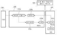
도 2는 종래의 TCXO(Temperature Compensated X-tal Oscillator)회로, 위상동기회로 및 전압제어발진기회로의 연결구성을 개략적으로 도시한 블록도. 2 is a block diagram schematically illustrating a connection configuration of a conventional Temperature Compensated X-tal Oscillator (TCXO) circuit, a phase synchronization circuit, and a voltage controlled oscillator circuit.
도 3은 종래의 전압제어발진기회로 전원부의 구조를 예시적으로 도시한 회로도. 3 is a circuit diagram illustrating a structure of a conventional voltage controlled oscillator circuit power supply unit.
도 4는 본 발명의 실시예에 따른 TCXO회로, 위상동기회로 및 전압제어발진기회로의 연결구성을 개략적으로 도시한 블록도.4 is a block diagram schematically illustrating a connection configuration of a TCXO circuit, a phase synchronization circuit, and a voltage controlled oscillator circuit according to an embodiment of the present invention.
도 5는 본 발명의 실시예에 따른 전압제어발진기회로의 구성요소를 도시한 회로도.5 is a circuit diagram showing components of a voltage controlled oscillator circuit according to an embodiment of the present invention.
도 6은 본 발명의 실시예에 따른 공진부에서 처리되는 발진 신호의 파형을 도시한 그래프.6 is a graph showing waveforms of an oscillation signal processed in a resonator according to an exemplary embodiment of the present invention.
도 7은 종래의 실시예에 따른 전압제어발진기회로의 공진부에서 처리되는 발진신호를 확대하여 도시한 그래프.7 is an enlarged graph illustrating an oscillation signal processed in a resonance unit of a voltage controlled oscillator circuit according to a conventional embodiment.
도 8은 본 발명의 실시예에 따른 전압제어발진기회로의 공진부에서 처리되는 발진신호를 확대하여 도시한 그래프.8 is an enlarged graph illustrating an oscillation signal processed in a resonance unit of a voltage controlled oscillator circuit according to an exemplary embodiment of the present invention.
〈도면의 주요 부분에 대한 부호의 설명〉<Explanation of symbols for main parts of drawing>
700: 전압제어발진기회로 710: 공진부700: voltage controlled oscillator circuit 710: resonator
720: 필터부 730: 전원부 720: filter unit 730: power unit
본 발명은 전압제어발진기(VCO;Voltage controlled oscillator)회로에 관한 것이다.The present invention relates to a voltage controlled oscillator (VCO) circuit.
최근 들어 휴대폰을 비롯한 무선 송수신 시스템의 발전이 가속화되고 있다. 즉, 초창기의 무선 송수신 시스템은 상대방과 전화를 하고 간단한 단문 메시지(SMS)를 전송하던 것이었으나, 현재는 대용량의 방송 프로그램이나 영화를 서비스하는 주문형 비디오 서비스(VOD)를 제공하고 디지털 카메라처럼 고해상도의 사진을 획득하고 캠코더처럼 동영상을 녹화할 수 있으며, 또한 사진이나 동영상을 상대방에게 전송할 수도 있다.Recently, the development of wireless transmission and reception systems including mobile phones is accelerating. In other words, in the early days, the wireless transmission / reception system used to make a call with the other party and transmit a simple short message (SMS), but now it provides a video-on-demand (VOD) service that provides a large broadcast program or a movie, You can take a picture, record a video like a camcorder, and send a picture or video to the other party.
이처럼 무선 송수신 시스템은 음성통화 외에도 여러 가지 기능이 부가됨에 따라 각각의 기능을 수행할 수 있는 장치를 구비할 필요가 생겼으며, 이는 무선 송수신 시스템의 전체적인 사이즈를 커지게 하였다.As described above, the wireless transmission / reception system needs to include a device capable of performing each function as various functions are added in addition to voice calls, which increases the overall size of the wireless transmission / reception system.
그러나 무선 송수신 시스템은 다양한 기능을 수행하면서도 휴대하기에 편리해야 하므로 무선 송수신 시스템의 소형화와 수신성능의 개선이 요구된다.However, since the wireless transmit / receive system should be convenient to carry while performing various functions, the miniaturization of the wireless transmit / receive system and improvement of reception performance are required.
따라서, 각각의 기능을 수행하는 회로구성 또는 칩(chip)의 소형화와 더불어 여러 기능을 함께 수행할 수 있는 프론트 엔드 모듈(Front end module)로 구현된 무선 송수신 시스템이 개발되었는데, 단일 모듈로 구현된 무선 송수신 시스템의 경우에는 간섭 현상 때문에 전원을 안정적으로 공급할 수 없는 문제가 발생한다.Therefore, a wireless transceiver system implemented as a front end module capable of performing various functions together with a miniaturization of a circuit configuration or a chip performing each function has been developed. In the case of a wireless transmission / reception system, there is a problem in that power cannot be stably supplied due to interference.
특히 수신성능에 큰 영향을 주는 전압제어발진기회로의 전원 잡음성분은 무선 송수신 시스템의 수신단에 많은 영향을 주기 때문에 무선 송수신 시스템의 전체적인 성능이 떨어진다는 문제점이 있다. In particular, the power source noise component of the voltage controlled oscillator circuit, which greatly affects the reception performance, has a lot of effects on the receiving end of the wireless transmission / reception system.
이하에서는 무선 송수신 시스템 중 대표적인 CDMA 이동통신단말기에 대해서 살펴보도록 한다.Hereinafter, a representative CDMA mobile communication terminal among wireless transmission / reception systems will be described.
도 1은 종래의 CDMA 이동통신단말기의 구성요소를 개략적으로 도시한 블록 회로도이다.1 is a block circuit diagram schematically showing the components of a conventional CDMA mobile communication terminal.
도 1에 의하면, 종래의 CDMA 이동통신단말기(1000)는 베이스밴드부(100), 신호처리부(200), 프런트엔드부(300), GPS부(400), TCXO(500)를 포함하여 구성된다.Referring to FIG. 1, a conventional CDMA
우선, 상기 베이스밴드부(100)는 신호처리부(200)로부터 전달받은 입력신호를 처리하고, 처리된 디지털 신호를 신호처리부(200)로 전달하여 송신한다.First, the
상기 신호처리부(200)는 수신 측 신호처리부(240)와 송신 측 신호처리부(220)로 구성된다.The
송신 측 신호처리부(220)은 다수개의 증폭기(221, 222, 224, 225), 주파수혼합기(223, 226), 송신 측 전압제어발진기회로(227), 송신 측 위상동기회로(228) 및 수신 측 위상동기회로(229)를 구비하고, 상기 베이스밴드부(100)에서 전달받은 디지털 신호를 RF신호로 전환한다.The transmitter
수신 측 신호처리부(240)는 LPF(245), 수신 측 전압제어발진기회로(241), 다수개의 주파수혼합기(242, 243) 및 합성기(244)를 구비하고, 프런트엔드부(300)에서 전달받은 RF신호를 중간주파수신호로 전환한다. The receiver
상기 프런트엔드부(300)는 송신BPF(310), 수신BPF(340), 전력증폭기(320), 저잡음증폭기(350), 듀플렉서(330) 및 다이플렉서(360)를 구비하고, 상기 베이스밴드단부(100)로부터 전달받은 RF신호를 안테나를 통해 송신하거나 안테나로부터 수신받은 RF신호를 신호처리부(200)로 전달한다.The
상기 GPS부(400)는 BPF(430), 저잡음증폭기(420) 및 주파수혼합기(410)를 구비하며 안테나로부터 수신받은 RF신호중 GPS신호만을 분리하여 신호처리부(200)로 전달한다.The
그런데, CDMA 이동통신단말기(1000)의 수신신호 레벨은 -110dBm 내지 -25dBm으로 매우 넓은 범위에서 움직이게 되므로 수신 단의 전압제어발진기의 전원부는 수신 단에 영향을 주는 중요한 요인으로 작용한다. 특히 수신단 전압제어발진기회로의 위상잡음은 수신신호 감도에 많은 영향을 주는 중요한 요인이 되는데, 아래에서 자세히 살펴보도록 한다. However, since the received signal level of the CDMA
도 2는 종래의 TCXO(Temperature Compensated X-tal Oscillator)회로, 위상동기회로 및 전압제어발진기회로의 연결구성을 개략적으로 도시한 블록도이다. 2 is a block diagram schematically illustrating a connection configuration of a conventional TCXO (Temperature Compensated X-tal Oscillator) circuit, a phase synchronization circuit, and a voltage controlled oscillator circuit.
도 2에 의하면, 상기 전압제어발진기회로(241)는 이동통신단말기의 베이스밴드부(100)로 기준주파수신호를 제공하는 회로로서, 상기 기준주파수신호는 중간주파수신호의 합성에 이용된다. 2, the voltage controlled
그러나, 가령 온도와 같은 외부 환경의 변화 요인에 의하여 전압제어발진기회로(241)가 제공하는 기준주파수신호는 미세하게 유동되어 불안정한 상태가 될 수 있으며, 이러한 경우 베이스밴드부(100)에서 처리되는 중간주파수신호에 왜곡이 발생 될 수 있다. However, for example, the reference frequency signal provided by the voltage controlled
이러한 이유로 전압제어발진기회로(241)의 기준주파수신호에 안정화를 위하여, TCXO회로(500)와 위상동기회로(229)가 구비되는데, 상기 위상동기회로(229)는 전압제어발진기회로(241)로부터 베이스밴드부(100)로 전달되는 기준주파수를 검출하여 TCXO회로(500)에서 제공되는 발진주파수신호와 비교하고, 주파수 차이에 대응되는 제어신호를 생성하여 상기 전압제어발진기회로(241)로 출력한다.For this reason, in order to stabilize the reference frequency signal of the voltage controlled
따라서, 상기 기준주파수신호가 유동되는 경우 위상동기회로(229)가 이를 검출하여 제어신호를 생성/전달하므로 상기 전압제어발진기회로(241)는 제어신호에 따라 안정적인 기준주파수의 출력을 유지할 수 있다. Accordingly, when the reference frequency signal flows, the
그러나, 상기 전압제어발진기회로(241)의 전원부(241b)에서 상기 공진부(241a)로 전원을 제공할 때, 상기 TCXO회로(500)와 위상동기회로(229)만으로는 전원에 섞인 잡음 성분에 의한 요인이 제거될 수 없으므로, 안정적인 기준주파수의 출력이 유지되지 않을 수 있다. However, when the
도 3은 종래의 전압제어발진기회로의 전원부의 구조를 예시적으로 도시한 회로도이다. 3 is a circuit diagram exemplarily illustrating a structure of a power supply unit of a conventional voltage controlled oscillator circuit.
도 3에 의하면, 전압제어발진기(VCO;Voltage controlled oscillator) 회로의 전원부 구조가 도시되어 있는데, DC 전압과 바이패스(bypass) 커패시터가 병렬로 연결된다.Referring to FIG. 3, there is shown a power supply structure of a voltage controlled oscillator (VCO) circuit, in which a DC voltage and a bypass capacitor are connected in parallel.
전압제어발진기회로는 직류전력을 교류전력으로 변환하는 에너지 변환 회로로서, 전압제어발진기회로의 전원부에는 DC 전압이 연결되어 전압제어발진기회로에 에너지를 공급한다. The voltage controlled oscillator circuit is an energy conversion circuit for converting DC power into AC power, and a DC voltage is connected to a power supply unit of the voltage controlled oscillator circuit to supply energy to the voltage controlled oscillator circuit.
이때 바이패스 커패시터는 공진 주파수일 때의 노이즈 성분을 제거하는 역할을 하지만 특정한 주파수 대역의 노이즈 성분만이 제거되어 전원부의 위상잡음을 개선하기에 부족하다. At this time, the bypass capacitor removes the noise component at the resonance frequency, but only the noise component of the specific frequency band is removed, which is insufficient to improve the phase noise of the power supply unit.
일반적으로 상기 CDMA 이동통신단말기(1000)의 구성 및 기능은 위에서 서술한 바와 같으며, 신호처리부(200)에서 RF신호를 중간주파수신호로 전환할 때 전압제어발진기로부터 전달된 기준주파수신호가 필요하다.In general, the configuration and function of the CDMA
그런데, 전압제어발진기회로가 단일 모듈로 구현될 경우 위상잡음이 혼재될 확률이 높으며, 이는 수신단 성능을 저하시키는 주요인이 된다. 특히 무선 송수신 시스템을 단일 모듈로 구현할 경우 전원의 위상잡음이 심각해지는 문제가 있다.However, when the voltage-controlled oscillator circuit is implemented as a single module, there is a high probability that phase noise is mixed, which is a major cause of deteriorating the receiver performance. In particular, when a wireless transmission / reception system is implemented as a single module, there is a problem in that phase noise of a power source becomes serious.
즉, 단일모듈로 구현된 무선 송수신 시스템의 경우에는 성능과 사이즈가 상반된 요소로서 전압제어발진기로 안정적인 전원을 공급하는 회로를 단일모듈로 구성할 필요성이 제기되고 있다.In other words, in the case of a wireless transmission / reception system implemented with a single module, there is a need to configure a circuit for supplying stable power to a voltage controlled oscillator as a single module as a factor in which performance and size are in conflict.
따라서, 본 발명은 프론트 엔드 모듈(Front end module)로 구현된 무선 송수신 시스템에 있어서, 전압제어발진기(VCO;Voltage controlled oscillator)회로 전원의 위상잡음 성분을 효과적으로 제거하는 전원단 구조를 제공하는 것을 그 목적 으로 한다. Accordingly, the present invention provides a power stage structure for effectively removing phase noise components of a voltage controlled oscillator (VCO) circuit power source in a wireless transmit / receive system implemented as a front end module. The purpose.
상기의 목적을 달성하기 위하여, 본 발명에 의한 전압제어발진기(VCO;Voltage controlled oscillator)회로는 무선 송수신 시스템에 관한 것으로서, 전원을 공급하는 전원부; 상기 전원부로부터 전원을 인가받아 기준주파수신호를 생성하고 상기 기준주파수 신호를 상기 무선 송수신 시스템의 베이스밴드부로 제공하는 공진부; 및 상기 전원부 및 상기 공진부 사이에 연결되고 상기 전원의 위상잡음을 필터링하는 필터부를 포함한다.In order to achieve the above object, the voltage controlled oscillator (VCO) circuit according to the present invention relates to a wireless transmission and reception system, a power supply for supplying power; A resonator configured to receive power from the power supply unit to generate a reference frequency signal and to provide the reference frequency signal to a baseband unit of the wireless transmission / reception system; And a filter unit connected between the power supply unit and the resonator unit to filter phase noise of the power supply unit.
상기의 다른 목적을 달성하기 위하여, 본 발명에 의한 프론트 엔드 모듈은 무선 송수신 시스템에 관한 것으로서, 전원을 공급하는 전원부; 상기 전원부로부터 전원을 인가받아 기준주파수신호를 생성하고 상기 기준주파수 신호를 상기 무선 송수신 시스템의 베이스밴드부로 제공하는 공진부; 및 상기 전원부 및 상기 공진부 사이에 연결되고 상기 전원의 위상잡음을 필터링하는 필터부를 포함한다.In order to achieve the above object, the front end module according to the present invention relates to a wireless transmission and reception system, a power supply for supplying power; A resonator configured to receive power from the power supply unit to generate a reference frequency signal and to provide the reference frequency signal to a baseband unit of the wireless transmission / reception system; And a filter unit connected between the power supply unit and the resonator unit to filter phase noise of the power supply unit.
이하에서 첨부된 도면을 참조하여 본 발명의 실시예에 따른 전압제어발진기회로에 대하여 상세히 설명하는데, 상기 전압제어발진기회로는 CDMA 이동통신단말기에 적용되는 것으로 한다.Hereinafter, a voltage controlled oscillator circuit according to an embodiment of the present invention will be described in detail with reference to the accompanying drawings. The voltage controlled oscillator circuit will be applied to a CDMA mobile communication terminal.
도 4는 본 발명의 실시예에 따른 TCXO회로(500), 위상동기회로(Rx PLL; Phase Locked Loop)(600) 및 전압제어발진기회로(700)의 연결구성을 개략적으로 도시한 블록도이다.4 is a block diagram schematically illustrating a connection configuration of a
도 4에 의하면, 상기 전압제어발진기회로(700)는 이동통신단말기의 베이스밴 드부(800)로 기준주파수신호를 제공하는 회로로서, 공진부(710), 필터부(720), 전원부(730)를 구비한다. Referring to FIG. 4, the voltage controlled
상기 전압제어발진기회로(700)로부터 전달된 기준주파수신호는 이동통신단말기의 베이스밴드부(800)에서 중간주파수 합성에 이용되므로 상기 전압제어발진기회로(700)는 안정적인 신호를 전달해야 한다. Since the reference frequency signal transmitted from the voltage controlled
그러나, 가령 온도와 같은 외부 환경 변화 요인 및 상기 전원부(730)에서 전원 제공시 발생되는 잡음성분 등에 의해서 전압제어발진기회로(700)가 제공하는 기준주파수신호는 미세하게 유동되어 불안정한 상태가 될 수 있으며, 이러한 경우 베이스밴드부(800)에서 처리되는 중간주파수신호에 왜곡이 발생 될 수 있다.However, the reference frequency signal provided by the voltage controlled
따라서, 안정적인 기준주파수신호를 전달하기 위해서는 온도와 같은 외부 요인과 상기 전원부(730)의 위상잡음을 개선할 필요가 있다. Therefore, in order to deliver a stable reference frequency signal, it is necessary to improve external factors such as temperature and phase noise of the
먼저, 온도와 같은 외부 환경 변화 요인을 제거하여 전압제어발진기회로(700)의 기준주파수신호의 안정화를 위하여, TCXO회로(500)와 위상동기회로(600)가 구비되는데, 상기 위상동기회로(600)는 전압제어발진기회로(700)로부터 베이스밴드부(800)로 전달되는 기준주파수신호를 검출하여 TCXO회로(500)에서 제공되는 발진주파수신호와 비교하고, 주파수 차이에 대응되는 제어신호를 생성하여 상기 전압제어발진기회로(700)로 출력한다.First, the
따라서, 상기 기준주파수신호가 유동되는 경우 위상동기회로(600)가 이를 검출하여 제어신호를 생성/전달하므로 상기 전압제어발진기회로(700)는 제어신호에 따라 안정적인 기준주파수의 출력을 유지할 수 있다.Therefore, when the reference frequency signal flows, the
상기 TCXO회로(500)는 수정발진기에서 온도변화에 따른 주파수 교란을 통제하는 장치로서, 온도변화에 대하여 일정한 값의 주파수를 갖는 발진주파수신호를 상기 위상동기회로(600)로 제공한다.The
주로, TCXO회로(500)는 큰 온도의 변화(보통, 영하 30도 내지 영상 75도)에도 2.5ppm을 초과하여 주파수가 교란되지 않고 일정하게 고정된 주파수신호를 발진한다.Mainly, the
상기 위상동기회로(600)는 주파수검출기(610), 분주기(620), 챠지펌프(charge pump)(630), 루프필터(loop filter)(640)를 포함하여 구성된다.The
상기 주파수검출기(610)는 TCXO회로(500)로부터 발진주파수신호를 입력받고, 상기 전압제어발진기회로(700)로부터 출력되는 기준주파수신호를 검출하여 비교한다.The
일반적으로 상기 전압제어발진기회로(700)가 제공하는 기준주파수신호는 고주파수(가령, "㎓" 단위의 주파수신호)신호이며, 상기 TCXO회로(500)가 제공하는 발진주파수신호는 기준주파수신호에 비해서 상대적으로 낮은주파수신호(가령, "㎒" 단위의 주파수신호)이다.In general, the reference frequency signal provided by the voltage controlled
따라서, 상기 주파수검출기(610)는 기준주파수신호와 발진주파수신호의 주파수를 비교하기 위해서, 기준주파수신호는 분주기(620)를 통해 상대적으로 낮은 주파수로 전환되어야 한다.Therefore, in order to compare the frequency of the reference frequency signal and the oscillation frequency signal, the
예를 들어, 상기 TCXO회로(500)가 100㎒의 발진주파수신호를 제공하고 상기 전압제어발진기회로(700)가 1.1㎓의 기준주파수신호를 제공하면, 분주기는 기준주 파수신호를 1/10배 하여 비교가능한 단위의 신호로 변환한다.For example, if the
상기 주파수검출기(610)는 발진주파수신호 및 전환된 기준주파수신호의 주파수를 비교하여 주파수 차이에 대응되는 제어신호를 챠지펌프(630)로 전달하고 챠지펌프(630)는 제어신호에 따라 전류값을 조정한다.The
상기 예시에 의하면, TCXO회로(500)의 100MHz의 발진주파수신호와 전환된 110MHz의 기준주파수신호가 비교되고, 주파수검출기(610)는 발진주파수신호와 기준주파수신호의 차이, 즉 10MHz의 차이에 대응되는 전류량을 가지는 제어신호를 생성한다.According to the above example, the 100 MHz oscillation frequency signal of the
상기 챠지펌프(630)는 제어신호에 따라 특정량의 전하를 공급하거나 흡수하는 전자회로이다.The
즉, 챠지펌프(630)는 발진주파수신호에 비하여 기준주파수신호의 전압이 크면 분기회로에 의하여 특정량의 전하를 루프필터(640)로 공급하고, 기준주파수신호의 전압이 발진주파수신호에 비하여 작으면 분기회로에 의하여 특정량의 전하를 로우패스필터(Low Pass Filter)(640)로부터 끌어당긴다.That is, the
상기 제어신호에 따라 전류량이 조정된 제어신호는 로우패스필터(640)로 전달되는데, 가령 커패시터 2개와 저항 1개로 구성된 2차 필터를 이용할 수 있다.The control signal whose current amount is adjusted according to the control signal is transmitted to the
상기 저항과 병렬로 연결된 커패시터에서는 상기 챠지펌프(630)에서 밀고 당기는 전하량을 조절하여 상기 전압제어발진기회로(700)의 전압을 조정하고, 상기 위상동기회로(600)에서 발생하는 스퓨리어스 특성을 감소시킨다. The capacitor connected in parallel with the resistor adjusts the amount of charge and push of the
일반적으로, 상기 수신 측 위상동기회로(600)의 상기 주파수검출기(610), 상 기 분주기(620), 상기 챠지펌프(630)는 송신 칩에 배치되고, 상기 로우패스필터(640)는 수신 칩에 배치될 수 있다.In general, the
다음으로, 전압제어발진기회로(700)가 프론트 엔드 모듈로 구현될 경우, 위상잡음이 혼재될 확률이 높아져 수신성능에 영향을 미치므로, 상기 전원부(730)의 위상잡음을 개선할 필요가 있다.Next, when the voltage controlled
상기 전원부(730)의 위상잡음을 개선하기 위해서, 상기 전원부(730)와 상기 공진부(710) 사이에 상기 필터부(720)를 구비하는데, 상기 필터부(720)는 상기 전원부(730)에서 상기 공진부(710)로 전원 제공시 위상성분을 커패시터를 통하여 제거한다. In order to improve phase noise of the
따라서, 상기 전원부(730)로부터 위상잡음이 개선된 전원을 공급받아 상기 전압제어발진기회로(700)가 베이스밴드부(800)로 안정적인 기준주파수를 제공할 수 있다. Accordingly, the voltage controlled
본 발명의 상기 CDMA 이동통신단말기에서는 수신 측 위상동기회로(600)의 구성부분인 주파수검출기(610), 분주기(620), 챠지펌프(630)는 상기 CDMA 이동통신단말기의 송신 칩에 포함될 수 있다.In the CDMA mobile communication terminal of the present invention, the
그런데, CDMA 이동통신단말기의 수신레벨은 -110dBm 내지 -25dBm으로 매우 넓은 범위이며, 수신 측 전압제어발진기회로(700)의 잡음성분은 수신성능에 많은 영향을 준다. However, the reception level of the CDMA mobile communication terminal is in a very wide range of -110dBm to -25dBm, and the noise component of the receiver side voltage controlled
이하에서, 전압제어발진기회로(700)의 잡음성분을 개선하기 위한 구조를 살펴보도록 한다. Hereinafter, a structure for improving the noise component of the voltage controlled
도 5는 본 발명의 실시예에 따른 전압제어발진기회로(700)의 구성요소를 예시적으로 도시한 회로도이다.5 is a circuit diagram illustrating components of the voltage controlled
도 5에 의하면, 상기 전압제어발진기회로(700)는 전원을 공급하는 전원부(730), 상기 전원부(730)로부터 전원을 인가받아 기준주파수신호를 생성하고 상기 기준주파수 신호를 CDMA 이동통신단말기의 베이스밴드부로 제공하는 공진부(710), 및 상기 전원부(730)와 상기 공진부(710) 사이에 연결되고 상기 전원의 위상잡음을 필터링하는 필터부(720)를 포함하여 이루어진다.Referring to FIG. 5, the voltage controlled
먼저, 상기 전원부(730)는 이동통신단말기의 DC 전원단과 연결되어 전압제어발진기회로(700)로 에너지를 공급하는데, 상기 전원부(730)는 DC전원단과 병렬연결된 바이패스 커패시터를 구비하여 전원의 잡음 성분을 제거한다.First, the
상기 필터부(720)는 병렬연결된 저항 및 커패시터를 포함하여 이루어지는 필터단이 적어도 하나 이상 구비된다. 상기 필터부(720)는 상기 전원부(730)에서 공급되는 전원의 위상잡음을 개선한다. The
가령, 상기 필터부(720)는 병렬연결된 제1저항 및 제1커패시터로 이루어진 제1필터단과, 병렬연결된 제2저항 및 제2커패시터로 이루어진 제2필터단, 2개의 필터단이 직렬연결되어 구성될 수 있으며 2차에 걸쳐 위상잡음을 필터링한다. For example, the
상기 공진부(710)는 TCXO회로(500)로부터 제공된 발진주파수신호와 상기 공진부(710)에서 생성된 기준주파수신호의 주파수를 비교하여 주파수 차이에 따라 제어신호를 생성하는 위상동기회로(600)와 연결되고, 상기 공진부(710)는 상기 제어신호를 입력받아 상기 위상동기회로(600)로부터 입력된 제어신호에 대응되는 기준 주파수신호를 생성한다.The
또한, 상기 공진부(710)는 생성된 기준주파수신호를 베이스밴드부로 제공하는데, 이렇게 제공된 기준주파수신호는 주파수합성기(Mixer)에서 이용될 수 있다.In addition, the
상기 전압제어발진회로(700)의 전원부(730), 공진부(710), 필터부(720)는 CDMA 이동통신단말기의 수신 칩에 내장되고, 상기 수신 칩에 내장된 상기 공진부(710)는 수신 측의 베이스밴드부로 기준주파수신호를 제공한다.The
그리고, 상기 CDMA 이동통신단말기는 프론트 엔드 모듈(Front end module)로 구현된 것으로서, 상기 전원부(730), 상기 공진부(710), 상기 필터부(720)는 상기 프론트 엔드 모듈 내부에 구현된다.The CDMA mobile communication terminal is implemented as a front end module, and the
도 6은 본 발명의 실시예에 따른 공진부에서 처리되는 발진 신호의 파형을 도시한 그래프이고, 도 7은 종래의 실시예에 따른 전압제어발진기회로의 공진부에서 처리되는 발진신호를 확대하여 도시한 그래프이다. 또한, 도 8은 본 발명의 실시예에 따른 전압제어발진기회로의 공진부에서 처리되는 발진신호를 확대하여 도시한 그래프이다.6 is a graph illustrating waveforms of an oscillation signal processed in a resonator according to an exemplary embodiment of the present invention, and FIG. 7 is an enlarged diagram illustrating an oscillation signal processed in a resonator of a voltage controlled oscillator circuit according to a conventional embodiment. One graph. 8 is an enlarged graph illustrating an oscillation signal processed in a resonator of a voltage controlled oscillator circuit according to an exemplary embodiment of the present invention.
각 그래프의 가로축은 주파수 대역을 나타내며, 세로축은 전력을 의미한다.The horizontal axis of each graph represents a frequency band, and the vertical axis represents power.
도 6에 의하면, 상기 공진부(710)를 구성하는 각 소자들은 1.764㎓ 영역에 에너지를 집중시키고, 전기적인 공진 현상을 일으켜 기준주파수신호를 발진시킨다.Referring to FIG. 6, each element constituting the
상기 공진부(710)는 기준주파수신호를 수신 측 베이스밴드부로 전달하는데, 이는 도 5에 도시된 커패시터 C1에 축적된 전하의 이동으로 이루어진다.The
도 7 및 도 8은 발진이 일어나는 기준주파수신호를 확대한 그래프로서, 도 7 은 종래의 전압제어발진기(241)의 출력값에 대한 파형으로서, 그래프의 기울기는 -100.83dBc/Hz 이다. 7 and 8 are enlarged graphs of reference frequency signals in which oscillation occurs, and FIG. 7 is a waveform of an output value of a conventional voltage controlled
도 8은 본 발명의 실시예에 따른 전압제어발진기(700)의 출력값에 대한 파형으로써, 그래프의 기울기는 -108.50dBc/Hz 이다(여기서, 1mW에 대한 현재의 신호 크기를 dBm으로 표현할 때, dBc는 dBm으로 표현되는 신호의 크기 차이를 나타내는 단위이다).8 is a waveform of the output value of the voltage controlled
본 발명에 의한 전압제어발진기의 출력파형은 2차 위상잡음 필터링을 실시한 결과로서 종래의 전압제어발진기의 출력파형에 비해서 8~9dBC/Hz 정도 개선되었음을 알 수 있다.It can be seen that the output waveform of the voltage controlled oscillator according to the present invention is improved by about 8 to 9 dBC / Hz as a result of performing the second phase noise filtering.
이상에서 본 발명에 대하여 그 바람직한 실시예를 중심으로 설명하였으나 이는 단지 예시일 뿐 본 발명을 한정하는 것이 아니며, 본 발명이 속하는 분야의 통상의 지식을 가진 자라면 본 발명의 본질적인 특성을 벗어나지 않는 범위에서 이상에 예시되지 않은 여러 가지의 변형과 응용이 가능함을 알 수 있을 것이다. 예를 들어, 본 발명의 실시예에 구체적으로 나타난 각 구성 요소는 변형하여 실시할 수 있는 것이다. 그리고 이러한 변형과 응용에 관계된 차이점들은 첨부된 청구 범위에서 규정하는 본 발명의 범위에 포함되는 것으로 해석되어야 할 것이다.The present invention has been described above with reference to the preferred embodiments, which are merely examples and are not intended to limit the present invention, and those skilled in the art to which the present invention pertains do not depart from the essential characteristics of the present invention. It will be appreciated that various modifications and applications are not possible that are not illustrated above. For example, each component specifically shown in the embodiment of the present invention can be modified. And differences relating to such modifications and applications will have to be construed as being included in the scope of the invention defined in the appended claims.
본 발명에 의한 전압제어발진회로에 의하면, 전압발진기회로 전원부의 위상 잡음을 제거함으로써, 무선 송수신 시스템의 수신측의 스퓨리어스(spurious) 특성, STD(Single Tone desensitization) 특성, IMD(Inter-Modulation distortion) 특성 이 개선되어 수신감도가 향상되고, 외부 전원의 영향 없이 안정적으로 수신단에 전원을 공급할 수 있는 효과가 있다. According to the voltage-controlled oscillation circuit according to the present invention, by removing the phase noise of the voltage oscillator circuit power supply portion, the spurious characteristics, the single tone desensitization (STD) characteristics, the inter-modulation distortion (IMD) characteristics of the receiving side of the radio transceiver system. The characteristic is improved, the reception sensitivity is improved, and there is an effect that can stably supply power to the receiver without the influence of external power.
또한, 전압제어발진기회로는 프론트 엔드 모듈로 구현된 무선 송수신 시스템의 수신단에 포함되는 것으로서, 안정적인 기준주파수 신호를 제공하면서도 프론트 엔드 모듈 제품의 사이즈를 최소화할 수 있는 효과가 있다. In addition, the voltage controlled oscillator circuit is included in the receiving end of the wireless transmission / reception system implemented as the front end module, thereby providing a stable reference frequency signal and minimizing the size of the front end module product.
Claims (6)
Priority Applications (2)
| Application Number | Priority Date | Filing Date | Title |
|---|---|---|---|
| KR1020050129850A KR100737059B1 (en) | 2005-12-26 | 2005-12-26 | Voltage controlled oscillator circuit |
| US11/518,165 US7768792B2 (en) | 2005-09-12 | 2006-09-11 | Front end module |
Applications Claiming Priority (1)
| Application Number | Priority Date | Filing Date | Title |
|---|---|---|---|
| KR1020050129850A KR100737059B1 (en) | 2005-12-26 | 2005-12-26 | Voltage controlled oscillator circuit |
Publications (2)
| Publication Number | Publication Date |
|---|---|
| KR20070068102A true KR20070068102A (en) | 2007-06-29 |
| KR100737059B1 KR100737059B1 (en) | 2007-07-06 |
Family
ID=38366595
Family Applications (1)
| Application Number | Title | Priority Date | Filing Date |
|---|---|---|---|
| KR1020050129850A Expired - Fee Related KR100737059B1 (en) | 2005-09-12 | 2005-12-26 | Voltage controlled oscillator circuit |
Country Status (1)
| Country | Link |
|---|---|
| KR (1) | KR100737059B1 (en) |
Family Cites Families (2)
| Publication number | Priority date | Publication date | Assignee | Title |
|---|---|---|---|---|
| US6181216B1 (en) * | 1999-07-19 | 2001-01-30 | General Instrument Corporation | Low phase-noise voltage controlled oscillator |
| AU766639B2 (en) * | 1999-09-01 | 2003-10-23 | Qualcomm Incorporated | Wideband voltage controlled oscillator with good noise immunity |
-
2005
- 2005-12-26 KR KR1020050129850A patent/KR100737059B1/en not_active Expired - Fee Related
Also Published As
| Publication number | Publication date |
|---|---|
| KR100737059B1 (en) | 2007-07-06 |
Similar Documents
| Publication | Publication Date | Title |
|---|---|---|
| CN101162266B (en) | GPS receivers and handheld electronic devices | |
| JPH07221667A (en) | Method for generation of signal of different frequencies in digital radiotelephone | |
| US7327993B2 (en) | Low leakage local oscillator system | |
| US8374283B2 (en) | Local oscillator with injection pulling suppression and spurious products filtering | |
| JP2014195295A (en) | Frequency synthesizer with multiple tuning loops | |
| JP2004516692A (en) | Method and apparatus for reducing PLL lock time | |
| KR100997491B1 (en) | Communication transmitter using offset phase locked loop | |
| KR100251582B1 (en) | Apparatus for automatically switching the second if frequency in dual band and dual mode transceiver | |
| KR100737059B1 (en) | Voltage controlled oscillator circuit | |
| JP2017135525A (en) | Oscillator circuit, radio communication apparatus and sensitivity suppression reduction method | |
| KR101007211B1 (en) | Wideband High Frequency Frequency Synthesizer for Avionics | |
| KR101193337B1 (en) | Phase locked loop of low power and sub-sampling tranceiver using the same | |
| KR100737789B1 (en) | Cordless phone architecture | |
| KR100355790B1 (en) | Dual band PLL synthesizer module | |
| KR20010091693A (en) | Direct conversion receiver minimizing local oscillator leakage and method thereof | |
| EP0655844A2 (en) | Method and apparatus for forming intermediate frequency signals | |
| JPS61103324A (en) | Synthesizer circuit of radio communication equipment | |
| JP3063346B2 (en) | Wireless transmission device | |
| KR101148422B1 (en) | Phase locked loop of low power | |
| JP3801493B2 (en) | Transceiver using local oscillator | |
| KR19980057483A (en) | Dual Band Transceiver in Cell Phone | |
| JP2003152586A (en) | Radio communications equipment, radio equipment, and radio communication system | |
| KR20010058285A (en) | Dual band PLL synthesizer module | |
| JPH08251045A (en) | Pll circuit module | |
| KR20000046539A (en) | Transmitting circuit of mobile communication terminal |
Legal Events
| Date | Code | Title | Description |
|---|---|---|---|
| A201 | Request for examination | ||
| PA0109 | Patent application |
St.27 status event code: A-0-1-A10-A12-nap-PA0109 |
|
| PA0201 | Request for examination |
St.27 status event code: A-1-2-D10-D11-exm-PA0201 |
|
| PN2301 | Change of applicant |
St.27 status event code: A-3-3-R10-R13-asn-PN2301 St.27 status event code: A-3-3-R10-R11-asn-PN2301 |
|
| R18-X000 | Changes to party contact information recorded |
St.27 status event code: A-3-3-R10-R18-oth-X000 |
|
| E902 | Notification of reason for refusal | ||
| PE0902 | Notice of grounds for rejection |
St.27 status event code: A-1-2-D10-D21-exm-PE0902 |
|
| P11-X000 | Amendment of application requested |
St.27 status event code: A-2-2-P10-P11-nap-X000 |
|
| P13-X000 | Application amended |
St.27 status event code: A-2-2-P10-P13-nap-X000 |
|
| E701 | Decision to grant or registration of patent right | ||
| PE0701 | Decision of registration |
St.27 status event code: A-1-2-D10-D22-exm-PE0701 |
|
| PG1501 | Laying open of application |
St.27 status event code: A-1-1-Q10-Q12-nap-PG1501 |
|
| GRNT | Written decision to grant | ||
| PR0701 | Registration of establishment |
St.27 status event code: A-2-4-F10-F11-exm-PR0701 |
|
| PR1002 | Payment of registration fee |
St.27 status event code: A-2-2-U10-U11-oth-PR1002 Fee payment year number: 1 |
|
| PG1601 | Publication of registration |
St.27 status event code: A-4-4-Q10-Q13-nap-PG1601 |
|
| PN2301 | Change of applicant |
St.27 status event code: A-5-5-R10-R13-asn-PN2301 St.27 status event code: A-5-5-R10-R11-asn-PN2301 |
|
| R18-X000 | Changes to party contact information recorded |
St.27 status event code: A-5-5-R10-R18-oth-X000 |
|
| LAPS | Lapse due to unpaid annual fee | ||
| PC1903 | Unpaid annual fee |
St.27 status event code: A-4-4-U10-U13-oth-PC1903 Not in force date: 20100703 Payment event data comment text: Termination Category : DEFAULT_OF_REGISTRATION_FEE |
|
| PC1903 | Unpaid annual fee |
St.27 status event code: N-4-6-H10-H13-oth-PC1903 Ip right cessation event data comment text: Termination Category : DEFAULT_OF_REGISTRATION_FEE Not in force date: 20100703 |
|
| PN2301 | Change of applicant |
St.27 status event code: A-5-5-R10-R13-asn-PN2301 St.27 status event code: A-5-5-R10-R11-asn-PN2301 |
|
| P22-X000 | Classification modified |
St.27 status event code: A-4-4-P10-P22-nap-X000 |
|
| R18-X000 | Changes to party contact information recorded |
St.27 status event code: A-5-5-R10-R18-oth-X000 |
|
| P22-X000 | Classification modified |
St.27 status event code: A-4-4-P10-P22-nap-X000 |
|
| R18-X000 | Changes to party contact information recorded |
St.27 status event code: A-5-5-R10-R18-oth-X000 |
|
| R18-X000 | Changes to party contact information recorded |
St.27 status event code: A-5-5-R10-R18-oth-X000 |
|
| PN2301 | Change of applicant |
St.27 status event code: A-5-5-R10-R13-asn-PN2301 St.27 status event code: A-5-5-R10-R11-asn-PN2301 |