KR20060095156A - Electroluminescent display with conductive mesh - Google Patents
Electroluminescent display with conductive mesh Download PDFInfo
- Publication number
- KR20060095156A KR20060095156A KR1020050016603A KR20050016603A KR20060095156A KR 20060095156 A KR20060095156 A KR 20060095156A KR 1020050016603 A KR1020050016603 A KR 1020050016603A KR 20050016603 A KR20050016603 A KR 20050016603A KR 20060095156 A KR20060095156 A KR 20060095156A
- Authority
- KR
- South Korea
- Prior art keywords
- electron emission
- substrate
- conductive mesh
- display device
- electrode
- Prior art date
- Legal status (The legal status is an assumption and is not a legal conclusion. Google has not performed a legal analysis and makes no representation as to the accuracy of the status listed.)
- Withdrawn
Links
Images


Classifications
-
- E—FIXED CONSTRUCTIONS
- E04—BUILDING
- E04F—FINISHING WORK ON BUILDINGS, e.g. STAIRS, FLOORS
- E04F19/00—Other details of constructional parts for finishing work on buildings
- E04F19/02—Borders; Finishing strips, e.g. beadings; Light coves
- E04F19/04—Borders; Finishing strips, e.g. beadings; Light coves for use between floor or ceiling and wall, e.g. skirtings
- E04F2019/0404—Borders; Finishing strips, e.g. beadings; Light coves for use between floor or ceiling and wall, e.g. skirtings characterised by the material
- E04F2019/0422—Borders; Finishing strips, e.g. beadings; Light coves for use between floor or ceiling and wall, e.g. skirtings characterised by the material of organic plastics with or without reinforcements or filling materials
-
- E—FIXED CONSTRUCTIONS
- E04—BUILDING
- E04F—FINISHING WORK ON BUILDINGS, e.g. STAIRS, FLOORS
- E04F19/00—Other details of constructional parts for finishing work on buildings
- E04F19/02—Borders; Finishing strips, e.g. beadings; Light coves
- E04F19/04—Borders; Finishing strips, e.g. beadings; Light coves for use between floor or ceiling and wall, e.g. skirtings
- E04F2019/0454—Borders; Finishing strips, e.g. beadings; Light coves for use between floor or ceiling and wall, e.g. skirtings with decorative effects
Landscapes
- Engineering & Computer Science (AREA)
- Architecture (AREA)
- Civil Engineering (AREA)
- Structural Engineering (AREA)
- Cathode-Ray Tubes And Fluorescent Screens For Display (AREA)
Abstract
본 발명은 제작 공정 중에 도전성 메쉬의 틀어짐을 방지할 수 있는 도전성 메쉬 고정 구조를 구비한 전자방출 표시장치에 관한 것이다. 본 발명에 따른 전자방출 표시장치는, 상부에 전자방출 영역이 형성되며 전자방출 영역 외곽에서 배면 기판 상에 접착되는 고정 부재 및 가이드 부재를 구비하는 전자방출기판과, 전자방출 영역으로부터 방출된 전자에 의해 발광하는 형광막이 형성되는 화상형성기판, 그리고 전자가 통과하는 복수의 홀 및 가이드 부재가 삽입되는 가이드 홀을 구비하며 고정 부재에 의해 한 지점이 전자방출기판에 고정되고 그 팽창 및 수축 방향이 가이드 부재에 의해 한 지점으로부터 방사상 방향으로 유도되는 도전성 메쉬를 포함한다.The present invention relates to an electron emission display device having a conductive mesh fixing structure that can prevent twisting of the conductive mesh during a fabrication process. An electron emission display device according to the present invention includes an electron emission substrate having a fixing member and a guide member having an electron emission region formed thereon and bonded to a rear substrate outside the electron emission region, and the electrons emitted from the electron emission region. An image forming substrate on which a fluorescent film emitting light is formed, and a plurality of holes through which electrons pass, and a guide hole into which a guide member is inserted, and a point is fixed to the electron emitting substrate by a fixing member and the expansion and contraction directions thereof are guided. And a conductive mesh guided in a radial direction from one point by the member.
전자방출 표시장치, 메쉬, 열팽창, 틀어짐, 고정 Emission Display, Mesh, Thermal Expansion, Distortion, Fixed
Description
도 1은 종래의 금속 메쉬를 구비한 전자방출 표시장치에 대한 단면도이다.1 is a cross-sectional view of a conventional electron emission display device having a metal mesh.
도 2a 내지 도 2d는 본 발명의 바람직한 실시예에 따른 도전성 메쉬를 구비한 전자방출 표시장치의 다양한 예를 나타내는 평면도이다.2A to 2D are plan views illustrating various examples of an electron emission display device having a conductive mesh according to an exemplary embodiment of the present invention.
도 3은 본 발명의 실시예에 따른 도전성 메쉬를 구비한 전자방출 표시장치의 일례를 나타내는 평면도이다.3 is a plan view illustrating an example of an electron emission display device having a conductive mesh according to an exemplary embodiment of the present invention.
도 4a는 도 3에 도시한 전자방출 표시장치의 도전성 메쉬의 주요 부분을 개략적으로 나타내는 부분 평면도이다.FIG. 4A is a partial plan view schematically illustrating a main part of the conductive mesh of the electron emission display shown in FIG. 3.
도 4b는 도 4a의 도전성 메쉬에 대응되는 캐소드 기판의 주요 부분을 개략적으로 나타내는 측면도이다.4B is a side view schematically showing a main part of a cathode substrate corresponding to the conductive mesh of FIG. 4A.
도 5는 도 3의 Ⅳ-Ⅳ선을 따라 취한 전자방출 표시장치의 부분 단면도이다.FIG. 5 is a partial cross-sectional view of the electron emission display device taken along line IV-IV of FIG. 3.
도 6은 도 3에 Ⅴ-Ⅴ선을 따라 취한 전자방출 표시장치의 부분 단면도이다.FIG. 6 is a partial cross-sectional view of the electron emission display device taken along the line VV of FIG. 3.
<도면의 주요 부분에 대한 부호의 설명><Explanation of symbols for the main parts of the drawings>
100: 캐소드 기판 110: 배면 기판100: cathode substrate 110: back substrate
120: 제1 전극 130: 제1 절연층120: first electrode 130: first insulating layer
140: 전자방출부 150: 제2 전극140: electron emission unit 150: second electrode
160: 제2 절연층 170: 고정 부재160: second insulating layer 170: fixing member
172, 174: 가이드 부재 200: 애노드 기판172 and 174
210: 전면 기판 220: 애노드 전극210: front substrate 220: anode electrode
230: 광차폐막 240: 형광막230: light shielding film 240: fluorescent film
300: 스페이서 400: 도전성 메쉬300: spacer 400: conductive mesh
500: 실링 부재500: sealing member
본 발명은 제작 공정 중에 도전성 메쉬의 틀어짐을 방지할 수 있는 도전성 메쉬 고정 구조를 구비한 전자방출 표시장치에 관한 것이다.The present invention relates to an electron emission display device having a conductive mesh fixing structure that can prevent twisting of the conductive mesh during a fabrication process.
일반적으로, 전자방출소자(Electron Emission Device)는 캐소드 전극과 게이트 전극 사이에 인가된 전계에 의한 양자 역학적인 터널링 효과(Tunneling effect)에 의해서 캐소드 전극에 전기적으로 접속된 전자방출부로부터 전자를 방출시키는 구조는 가진다. 이러한 전자방출소자는 전자방출부로 열음극을 이용하는 방식과 냉음극을 이용하는 방식이 있다. 냉음극을 이용하는 방식의 전자방출소자로는 FEA(Field Emitter Array)형, SCE(Surface Conduction Emitter)형, MIM(Metal Insulator Metal)형, MIS(Metal Insulator Semiconductor)형, 그리고 BSE(Balli stic electron Surface Emitting)형 등이 알려져 있다.In general, an electron emission device emits electrons from an electron emission unit electrically connected to the cathode by a quantum mechanical tunneling effect by an electric field applied between the cathode and the gate electrode. Has a structure. The electron emitting device has a method using a hot cathode and a cold cathode as an electron emitting unit. The electron-emitting devices using the cold cathode are Field Emitter Array (FEA), Surface Conduction Emitter (SCE), Metal Insulator Metal (MIM), Metal Insulator Semiconductor (MIS), and Ballistic Plastic Surface Emitting) is known.
이러한 전자방출소자를 이용하면, 전자방출 표시장치, 각종 백라이트, 리소그라피용 전자빔 장치 등을 구현할 수 있다. 그 중에서 전자방출 표시장치는, 전자방출소자를 형성하며 전자를 방출하는 캐소드 기판(cathode plate)과, 방출된 전자의 충돌에 의해 발광하는 형광막이 형성되는 애노드 기판(anode plate)으로 구성된다. 통상, 전자방출 표시장치에서 캐소드 기판은 캐소드 전극과 게이트 전극이 교차하는 매트릭스 형상으로 교차 영역에서 정의되는 다수의 단위 전자방출소자를 구비하고, 애노드 기판은 전자방출소자에서 방출된 전자들에 의해 빛을 내는 형광막과 이 형광막을 향해 전자들이 가속될 수 있도록 형광막에 전압을 인가하는 애노드 전극을 구비한다.By using the electron emitting device, an electron emitting display device, various backlights, and an electron beam device for lithography can be implemented. Among them, an electron emission display device includes a cathode plate which forms an electron emission element and emits electrons, and an anode plate on which a fluorescent film which emits light by collision of emitted electrons is formed. In general, in an electron emission display device, a cathode substrate includes a plurality of unit electron emission devices defined in an intersection area in a matrix shape where the cathode electrode and the gate electrode intersect, and the anode substrate is lighted by electrons emitted from the electron emission device. And a anode electrode for applying a voltage to the fluorescent film so that electrons can be accelerated toward the fluorescent film.
도 1은 종래의 메쉬를 구비한 전자방출 표시장치에 대한 단면도이다.1 is a cross-sectional view of a conventional electron emission display device having a mesh.
도 1을 참조하면, 종래의 전자방출 표시장치는 캐소드 기판(10), 애노드 기판(20), 이들 두 기판(10, 20)을 소정 간격으로 격리시키는 스페이서(spacer, 30), 및 금속 메쉬(metal mesh, 40)를 포함한다.Referring to FIG. 1, a conventional electron emission display device includes a
캐소드 기판(10)은 배면 기판(11) 상에 형성되는 캐소드 전극(12), 캐소드 전극(12) 위에 형성된 게이트 절연층(13), 게이트 절연층(13)의 관통홀(13a) 내에 형성되는 전자방출부(14), 및 게이트 절연층(13) 위에 형성되며 관통홀(13a)에 대응하는 게이트 홀(15a)을 구비하는 게이트 전극(15)을 구비한다. 애노드 기판(20)은 배면 기판(11)과 대향하는 전면 기판(21), 이 전면 기판(21) 상에 형성되는 애노드 전극(22), 이 애노드 전극(22) 위에 형성되는 형광막(23) 및 블랙 매트릭스 (24)를 포함한다. 스페이서(30)는 캐소드 기판(10)과 애노드 기판(20) 사이에 소정의 간격을 유지하는 역활을 한다. The
금속 메쉬(40)는 캐소드 기판(10) 상부에 밀착 고정된다. 이때, 금속 메쉬(40)와 캐소드 기판(10) 사이에는 상부 절연층(16)이 형성된다. 금속 메쉬(40)는 게이트 홀(15a)에 대응하는 메쉬 홀(42)을 구비한다.The
한편, 종래의 전자방출 표시장치에서는 예를 들어 약 420℃ 온도하에서의 형광막 소성시, 금속 메쉬의 변형 및 금속 메쉬의 변형으로 인하여 애노드 기판과의 정렬이 흐트러지는 문제가 발생된다. 특히, 진공 패키징시 가해지는 300℃ 이상의 공정 온도에서 2차적인 금속 메쉬의 변형 및 애노드 기판과의 오정렬이 발생된다. 이로 인해, 스페이서가 탈락되는 문제가 발생될 수 있다. 이것은 전자방출 표시장치의 고압 인가 환경과 빔 집속 환경을 악화시켜 양질의 제품을 만들기 어렵게 한다.On the other hand, in the conventional electron emission display device, when the fluorescent film is fired at a temperature of about 420 ° C., the alignment of the anode substrate is disturbed due to the deformation of the metal mesh and the deformation of the metal mesh. In particular, the secondary metal mesh deformation and misalignment with the anode substrate occur at a process temperature of 300 ° C. or higher applied during vacuum packaging. This may cause a problem that the spacer is dropped. This deteriorates the high-pressure application environment and the beam focusing environment of the electron emission display device, making it difficult to produce a good quality product.
이처럼, 종래의 금속 메쉬를 구비한 전자방출 표시장치에서는 고착 공정, 봉착 공정, 가열배기 공정 중에 금속 메쉬의 열팽창 및 틀어짐으로 인해 장치 내에 금속 메쉬를 정확하게 정렬시키기 어렵다는 문제점이 있다.As such, in the conventional electron emission display device having the metal mesh, it is difficult to accurately align the metal mesh in the device due to thermal expansion and twisting of the metal mesh during the fixing process, the sealing process, and the heat exhaust process.
본 발명은 상술한 종래 기술의 문제점을 고려하여 도출된 것으로, 그 목적은 제작 공정 중에 도전성 메쉬의 틀어짐을 방지할 수 있는 도전성 메쉬 고정 구조를 구비한 전자방출 표시장치를 제공하는 데 있다.SUMMARY OF THE INVENTION The present invention has been derived in view of the above-described problems of the prior art, and an object thereof is to provide an electron emission display device having a conductive mesh fixing structure capable of preventing twisting of the conductive mesh during a manufacturing process.
상술한 목적을 달성하기 위하여 본 발명의 제1 측면은, 상부에 전자방출 영역이 형성되며 상기 전자방출 영역 외곽에서 배면 기판 상에 접착되는 고정 부재 및 가이드 부재를 구비하는 전자방출기판; 상기 전자방출 영역으로부터 방출된 전자에 의해 발광하는 형광막이 형성되는 화상형성기판; 및 상기 전자가 통과하는 복수의 홀 및 상기 가이드 부재가 삽입되는 가이드 홀을 구비하며, 상기 고정 부재에 의해 한 지점이 상기 전자방출기판에 고정되고 그 팽창 및 수축 방향이 상기 가이드 부재에 의해 상기 한 지점으로부터 방사상 방향으로 유도되는 도전성 메쉬를 포함하는 전자방출 표시장치를 제공한다.In order to achieve the above object, a first aspect of the present invention provides an electron emission substrate having an electron emission region formed thereon and having a fixing member and a guide member adhered to a rear substrate outside the electron emission region; An image forming substrate on which a fluorescent film which emits light by electrons emitted from the electron emission region is formed; And a plurality of holes through which the electrons pass and a guide hole into which the guide member is inserted, wherein one point is fixed to the electron-emitting substrate by the fixing member, and the expansion and contraction direction thereof is determined by the guide member. An electron emission display device including a conductive mesh guided in a radial direction from a point is provided.
바람직하게, 상기 고정 부재는 상기 도전성 메쉬에 형성된 고정 홀에 삽입되고 소정의 접착 수단에 의해 고정적으로 접합된다.Preferably, the fixing member is inserted into the fixing hole formed in the conductive mesh and fixedly bonded by a predetermined bonding means.
또한, 상기 가이드 부재는 상기 가이드 홀 내에서 상기 방사상 방향으로 왕복 운동한다.Further, the guide member reciprocates in the radial direction within the guide hole.
또한, 상기 가이드 부재 및 상기 가이드 홀은 상기 방사상 방향으로 복수개 형성된다.In addition, the guide member and the guide hole are formed in plural in the radial direction.
이하, 첨부된 도면을 참조하여 본 발명에 따른 바람직한 실시예를 상세하게 설명하기로 한다. 이하의 설명에서 어떤 층이 다른 층의 위에 존재한다고 기술될 때, 이는 다른 층의 바로 위에 존재할 수도 있고, 그 사이에 제3의 층이 게재될 수 도 있다. 또한, 도면에서 각 층의 두께나 크기는 설명의 편의 및 명확성을 위하여 과장되었다. 도면상에서 동일 부호는 동일한 요소를 지칭한다.Hereinafter, exemplary embodiments of the present invention will be described in detail with reference to the accompanying drawings. In the following description, when a layer is described as being on top of another layer, it may be present directly on top of another layer, and a third layer may be interposed therebetween. In the drawings, the thickness and size of each layer are exaggerated for clarity and convenience of explanation. Like numbers refer to like elements in the figures.
도 2a 내지 도 2d는 본 발명의 바람직한 실시예에 따른 도전성 메쉬를 구비한 전자방출 표시장치의 다양한 예를 나타내는 평면도이다.2A to 2D are plan views illustrating various examples of an electron emission display device having a conductive mesh according to an exemplary embodiment of the present invention.
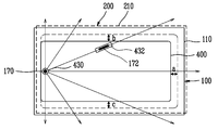
도 2a 내지 도 2d에 도시한 바와 같이, 본 발명에 따른 전자방출 표시장치는 배면 기판(110), 고정 부재(170) 및 가이드 부재(172)를 구비한 캐소드 기판(100)과, 전면 기판(210)을 구비한 애노드 기판(200), 그리고 고정 홀(430) 및 가이드 홀(432)을 구비한 도전성 메쉬(400)를 포함한다.2A to 2D, the electron emission display device according to the present invention includes a
캐소드 기판(100)의 고정 부재(170)는 일단이 캐소드 기판(100)의 배면 기판(110) 상에 소정의 접착 수단에 의해 고정적으로 부착되며, 타단이 도전성 메쉬(400)의 고정 홀(430)에 삽입되어 수정의 접착 수단에 의해 고정적으로 접착된다. 고정 부재(170)는 도전성 메쉬(400)의 일측면 가장자리 중앙부나, 가장자리 코너부 또는 중앙부에 고정점을 형성한다.One end of the
캐소드 기판(100)의 가이드 부재(172)는 도전성 메쉬(400)의 고정 홀(430)에 고정적으로 결합되는 고정 부재(170)를 중심으로 방사상 방향으로 연장되는 선상에 형성된다. 가이드 부재(172)는 소정의 두께와 폭을 가지고 연장되는 길이부를 가지며, 이때 길이부는 방사상 방향으로 연장된다. 또한, 가이드 부재(172)는 도전성 메쉬(400)에 형성된 가이드 홀(432)에 삽입되며 방사상 방향으로 왕복가능하게 결합된다.The
상술한 구성에 의해, 도전성 메쉬는 열공정을 포함하는 제작 공정 중에 팽창 및 수축 방향이 일정하게 유지된다. 따라서, 제작 공정 중에 도전성 메쉬의 틀어짐을 방지할 수 있다.By the above-described configuration, the conductive mesh has a constant expansion and contraction direction during the manufacturing process including the thermal process. Therefore, the twist of the conductive mesh can be prevented during the manufacturing process.
다음은 본 발명에 따른 도전성 메쉬를 구비한 전자방출 표시장치의 일례를 보다 상세히 설명한다. 도 3은 본 발명의 실시예에 따른 도전성 메쉬를 구비한 전자방출 표시장치의 일례를 나타내는 평면도이다. 도 4a는 도 3에 도시한 전자방출 표시장치에 채용된 도전성 메쉬의 주요 부분을 개략적으로 나타내는 부분 평면도이다. 그리고, 도 4b는 도 4a의 도전성 메쉬에 대응되는 캐소드 기판의 주요 부분을 개략적으로 보여주는 측면도이다.Next, an example of an electron emission display device having a conductive mesh according to the present invention will be described in detail. 3 is a plan view illustrating an example of an electron emission display device having a conductive mesh according to an exemplary embodiment of the present invention. 4A is a partial plan view schematically illustrating a main part of the conductive mesh employed in the electron emission display shown in FIG. 3. 4B is a side view schematically illustrating a main part of the cathode substrate corresponding to the conductive mesh of FIG. 4A.
도 3, 도 4a 및 도 4b를 참조하면, 전자방출 표시장치는 제작 공정 중에 도전성 메쉬의 틀어짐을 방지할 수 있는 구조를 갖는다. 이를 위해, 전자방출 표시장치는 고정 부재(170) 및 가이드 부재(172, 174)를 구비한 캐소드 기판(100)과, 애노드 기판(200), 그리고 캐소드 기판(100) 상에 밀착 형성되며 캐소드 기판(100)의 고정 부재(170) 및 가이드 부재(172, 174)가 삽입되는 고정 홀(162) 및 가이드 홀(164, 166)을 구비하는 도전성 메쉬(400)를 포함한다.3, 4A, and 4B, the electron emission display device has a structure capable of preventing the conductive mesh from twisting during the fabrication process. To this end, the electron emission display device is formed on the
여기서, 캐소드 기판(100)은 전자를 방출하는 전자방출 영역이 배면 기판(110)의 상부에 형성된 전자방출기판을 나타내며, 애노드 기판(200)은 캐소드 기판(100)의 전자방출 영역으로부터 방출된 전자의 충돌에 의해 발광하는 형광막이 전면 기판(210) 상에 형성된 화상형성기판을 나타낸다.Here, the
구체적으로, 캐소드 기판(100)은 전자방출 영역 외곽의 일측면 가장자리 중앙부에 형성되는 고정 부재(170)를 구비한다. 고정 부재(170)는 대략 원 기둥 모양이나 다각형 기둥 모양으로 형성되며, 그 일단이 소정의 접착 수단에 의해 배면 기판(110) 상에 고정적으로 접합된다.Specifically, the
또한, 캐소드 기판(100)은 고정 부재(170)가 형성되는 일측면 가장자리에 형성되는 가이드 부재(172, 174)를 구비한다. 가이드 부재(172, 174)는 고정 부재(170)를 지나는 직선 상에 그 길이 방향이 놓여지는 대략 직사각형 기둥 모양으로 형성되며, 그 일단이 소정의 접착 수단에 의해 배면 기판(110) 상에 고정적으로 접합된다.In addition, the
도전성 메쉬(400)는 고정 부재(170)의 타단이 삽입되는 고정 홀(162)을 구비한다. 고정 홀(162)에는 도전성 메쉬(400)와 고정 부재(170)를 접착시키는 소정의 접착 수단이 도포되며, 그것에 의해 도전성 메쉬(400)는 고정 부재(170)를 통해 캐소드 기판(100)에 고정된다.The
또한, 도전성 메쉬(400)는 가이드 부재(172, 174)가 끼우지며 도전성 메쉬(400)이 세 측면에 직교하는 방향으로 소정 길이(a, b, c)로 열팽창할 때, 도전성 메쉬(400)의 열팽창 방향을 제어할 수 있도록 가이드 부재(172, 174)를 원하는 방향으로 수용하는 가이드 홀(164, 166)을 구비한다. 가이드 홀(164, 166)은 가이드 부재(172, 174)가 미끄러져 움직일 수 있도록 형성된다.In addition, the
상술한 본 발명에 의하면, 도전성 메쉬의 일측면 가장자리 중심부를 캐소드 기판에 고정시키고, 그 일측면 가장자리에 가이드 구조를 형성함으로써, 400℃ 또 는 그 이상의 온도를 이용하는 고착 공정, 봉착 공정, 가열배기 공정 등의 전자방출 표시장치의 제작 공정 중에 도전성 메쉬가 열팽창하는 경우에도, 도전성 메쉬의 틀어짐을 방지할 수 있다.According to the present invention described above, by fixing the central portion of one side edge of the conductive mesh to the cathode substrate and forming a guide structure on the one side edge, the fixing step, the sealing step, and the heat exhaust step using a temperature of 400 ° C or higher. Even when the conductive mesh is thermally expanded during the manufacturing process of the electron emitting display device such as the above, the twisting of the conductive mesh can be prevented.
다음은 도 5 및 도 6을 참조하여 본 발명의 실시예에 따른 전자방출 표시장치를 보다 상세히 설명한다.Next, an electron emission display device according to an exemplary embodiment of the present invention will be described in more detail with reference to FIGS. 5 and 6.
도 5는 도 3의 Ⅳ-Ⅳ선을 따라 취한 전자방출 표시장치의 부분 단면도이고, 도 6은 도 3에 Ⅴ-Ⅴ선을 따라 취한 전자방출 표시장치의 부분 단면도이다.FIG. 5 is a partial cross-sectional view of the electron emission display device taken along line IV-IV of FIG. 3, and FIG. 6 is a partial cross-sectional view of the electron emission display device taken along line V-V in FIG. 3.
도 5 및 도 6을 참조하면, 전자방출 표시장치는 전자방출기판(100), 화상형성기판(200), 스페이서(300), 도전성 메쉬(400) 및 실링 부재(500)를 포함한다.5 and 6, the electron emission display device includes an
구체적으로, 전자방출기판(100)은 배면 기판(110), 제1 전극(120), 제1 절연층(130), 전자방출부(140), 제2 전극(150), 제2 절연층(160), 고정 부재(170) 및 가이드 부재(172, 174)를 포함한다.In detail, the
배면 기판(110)은 유리 기판이나 실리콘 기판을 사용한다. 특히, 탄소나노튜브(carbon nanotube, CNT) 페이스트를 이용하여 전자방출부(140)를 형성하는 경우, 배면 기판(110)은 후면 노광에 적합한 유리 기판을 사용한다.The
제1 전극(120)은 배면 기판(110) 상에 스트라이프(stripe) 상 또는 분절된 스트라이프 상으로 형성된다. 전자방출부(140)가 후면 노광 공정을 통해 형성되는 경우, 제1 전극(120)은 투명 전극, 예컨대 ITO(Indium Tin Oxide)로 형성된다. 본 실시예에 따른 잔자방출기판(100)의 제1 전극(120)은 그 구조상 전자방출 표시장치 의 캐소드 전극이 된다.The
제1 절연층(130)은 배면 기판(110)과 제1 전극(120) 상부에 형성되며, 제1 전극(120)과 제2 전극(150)을 전기적으로 상호 절연한다. 제1 절연층(130)은 절연 물질, 예컨대, PbO와 SiO2 혼합 유리질로 이루어지며, 제1 전극(120)을 부분적으로 노출시키는 복수의 제1 홀(132)을 구비한다. 제1 절연층(130)의 두께는 빔 집속에 적합하도록 후막 형성 공정에 의해 비교적 두껍게 형성된다.The first insulating
전자방출부(140)는 제1 절연층(130)에 구비된 제1 홀(132) 내에 노출되어 있는 제1 전극(120)에 전기적으로 접속되도록 형성된다. 전자방출부(140)는 카본계 물질 또는 나노미터(㎚) 사이즈 물질로 이루어진다. 이러한 전자방출부(140)에 사용가능한 물질로는 카본 나노튜브, 그라파이트(graphite), 그라파이트 나노파이버, 다이아몬드상 카본, C60, 실리콘 나노와이어 및 이들의 조합 물질이 있다.The
제2 전극(150)은 제1 절연층(130) 상에 소정의 형상으로 형성된다. 예컨대, 제2 전극(150)은 스프라이프 상으로 제1 전극(120)과 교차하는 방향으로 연장되며 제1 절연층(130)의 제1 홀(132)에 인접하게 형성된다. 본 실시예에서 제2 전극(150)은 전자방출기판(100)의 구조상 전자방출 표시장치의 게이트 전극이 된다. 이러한 제2 전극(150)은 전도성이 우수한 금속, 예컨대 금(Au), 은(Ag), 백금(Pt), 알루미늄(Al), 크롬(Cr) 및 이들의 합금 중에서 선택된 적어도 하나의 도전성 금속 재료로 형성된다. 제1 전극(120) 및 제2 전극(150)이 교차하는 영역은 전자방출 표시장치의 화소 영역으로 정의된다.The
제2 절연층(160)은 제2 전극(150)과 다른 인접한 제2 전극 사이에 배치되거나, 또는 전자방출기판(100) 전체의 기생 캐패시턴스의 영향을 무시할 수 있는 범위 내에서 인접한 제2 전극(150)의 일부와 겹치도록 배치될 수 있다. 제2 절연층(160)의 높이는 빔 집속을 위하여 10㎛ 내지 40㎛인 것이 바람직하며, 이는 전자방출부(140)로부터 방출된 전자가 도전성 메쉬(400)에 형성된 대응 홀로의 경로를 이탈하여 제2 절연층(160) 상부에 형성된 다른 요소에 충돌하여 전자가 축적될 가능성을 현저하게 감소시킨다. 제2 절연층(160)은 제1 전극(120), 제2 전극(150) 및 도전성 메쉬(400) 사이의 내전압 특성을 향상시키기 위하여 PbO 또는 SiO2를 포함하는 절연 재료로 형성되는 것이 바람직하다.The second
고정 부재(170)는 전자방출기판(100)의 전자방출 영역 외곽의 일측면 가장자리 중앙부에 형성된다. 고정 부재(170)의 일단은 제1 및 제2 절연층(130, 160)에 형성된 제1 개구부(162)에 삽입되며, 제1 개구부(162)에 도포되는 접착제 등의 접착 수단(440)에 의해 배면 기판(110) 상에 고정적으로 접합된다. 고정 부재(170)의 타단은 도전성 메쉬(400)에 형성된 고정홀(430)에 삽입되며, 고정홀(434)에 도포되는 접착 수단(440)에 의해 도전성 메쉬(400)와 접합된다. 이러한 구성에 의해, 도전성 메쉬(400)는 전자방출기판(100) 상부에 그 일측면 중앙부가 고정된다.The fixing
가이드 부재(172, 174)는 앞서 언급한 고정 부재(170)가 형성되는 전자방출기판(100)의 전자방출 영역 외곽의 일측면 가장자리에 형성된다. 가이드 부재(172, 174)는 고정 부재(170)를 지나는 직선 상에서 고정 부재(170)의 양쪽에 형성된다. 가이드 부재(172, 174)의 일단은 제1 및 제2 절연층(130, 160)에 형성된 제2 및 제3 개구부(164, 166)에 삽입되며, 제2 및 제3 개구부(164, 166)에 도포되는 접착 수단(440)에 의해 배면 기판(110) 상에 고정적으로 접합된다. 가이드 부재(172, 174)의 타단은 도전성 메쉬(400)에 형성된 제1 및 제2 가이드 홀(432, 434)에 유동적으로 끼워진다. 이러한 구성에 의해, 도전성 메쉬(400)는 제조 공정 중에 일시적으로 열팽창되는 경우에도 고정된 일측면의 중앙부를 중심으로 나머지 측면이 방사상으로 열팽창되었다가 다시 본래의 위치로 자연스럽게 복귀된다.The
이처럼, 본 발명에 의하면 전자방출 표시장치의 제작 공정 중에 도전성 메쉬의 틀어짐을 방지할 수 있다.As described above, according to the present invention, it is possible to prevent twisting of the conductive mesh during the manufacturing process of the electron emission display device.
다음으로, 화상형성기판(200)은 전면 기판(210)과, 전면 기판(210) 상부에 형성되는 애노드 전극(220), 형광막(230) 및 광차폐막(240)을 포함한다.Next, the
전면 기판(210)은 글래스 등의 투명한 재질로 형성된다. 전면 기판(210)은 전자방출기판(100)의 배면 기판(110)과 대향 배치된다.The
애노드 전극(220)은 투명한 재료로 형성되며, 전면 기판(210) 상의 유효 영역에 발광 영역을 형성하는 형광막(230)에 소정의 전압을 공급한다.The
형광막(230)은 전면 기판(210)의 일면에 형성되며 전자방출기판(100)의 전자방출부(140)에서 방출된 전자의 충돌에 의해 발광한다. 형광막(230)은 임의의 간격을 두고 소정의 형상, 예컨대 스트라이프 상으로 배치된다.The
광차폐막(240)은 선택적 구성 요소로서, 외부 빛을 흡수 및 차단하여 광학적 크로스 토크를 방지함으로써 콘트라스트가 향상되도록 형광막(230) 사이에 배치된 다. 다시 말해서, 광차폐막(240)은 전면 기판(210)의 유효 영역 내의 발광 영역 사이에 비발광 영역 또는 흑색 영역을 형성한다.The
한편, 화상형성기판(200)은 금속 박막(미도시)을 더 포함할 수 있다. 금속 박막은 형광막 상부에 위치하며 전자방출부로부터 방출된 전자를 보다 더 양호하게 집속하고 전자의 충돌에 의해 발광하는 빛을 전면 기판측으로 다시 반사시켜 반사효율을 향상시키는 역활을 한다. 또한, 금속 박막은 애노드 전극과 유사하게 형광막에 전압을 공급하도록 형성될 수 있다. 이러한 경우, 애노드 전극은 생략가능하다.On the other hand, the
다음으로, 스페이서(300)는 전자방출기판(100)과 화상형성기판(200)을 상호 지지한다. 스페이서(300)는 전자방출 표시장치 내부의 진공 환경하에서 전자방출기판(100)과 화상형성기판(200)을 소정 간격으로 유지시킨다.Next, the
다음으로, 도전성 메쉬(400)는 전자방출기판(100)의 전자방출 영역으로부터방출된 전자가 통과하는 제2 홀(420)을 구비한다. 도전성 메쉬(400)는 메쉬 형태의 도전성 시트를 나타낸다. 본 실시예에서, 도전성 메쉬(400)는 전자방출기판(100)과의 사이에 제2 절연층(160)을 개재하고 전자방출기판(100) 상부에 형성된다. 다른 한편으로, 본 발명에 따른 도전성 메쉬(400)는 스페이서(300)와의 접착에 의해 전자방출기판(100)과 소정 간격을 두고 고정 배치될 수 있다.Next, the
또한, 도전성 메쉬(400)는 화상형성기판(200)의 형광막(230)으로 향하는 전자를 집속하며, 아킹(arcing) 방전시의 전극 손상을 방지하는 역활을 한다. 예를 들면, 애노드 전극(220)에 인가되는 고전압에 의해 형성된 애노드 전계로부터 전자 방출기판(100)의 제2 전극(150), 전자방출부(140), 제1 전극(120) 등을 보호한다.In addition, the
또한, 도전성 메쉬(400)는 그 양면에 형성되는 소정의 메쉬 절연층(미도시)을 구비할 수 있다. 메쉬 절연층이 형성된 도전성 메쉬(400)를 이용하면, 전자방출 표시장치의 제작 공정 중의 도전성 메쉬(400)의 틀어짐을 더욱 방지할 수 있다. 또한, 도전성 메쉬(400)은 전자방출기판(100)을 형성하는 캐소드 공정과 별도의 공정을 통해서 형성되며, 메쉬 절연층은 글래스 프릿(미도시) 등에 의해 전자방출기판(100)의 제2 전극(150) 상부에 형성될 수 있다.In addition, the
다음으로, 실링 부재(500)는 전자방출기판(100)과 화상형성기판(200)을 진공 상태로 접합하기 위한 부재로서, 예컨대, 봉착용 프릿 바(frit bar)가 이용된다. 실링 부재(500)는 소정의 접착 페이스트에 의해 전자방출기판(100)과 화상형성기판(200)에 각각 접착된다.Next, the sealing
상술한 본 발명에 의하면, 전자방출 표시장치의 제작 공정 중에 열팽창하는 도전성 메쉬를 일정한 형태로 열팽창 및 수축되도록 제어함으로써 도전성 메쉬의 틀어짐을 방지할 수 있다. 따라서, 전자방출 표시장치의 고압 인가 환경과 빔 집속 환경을 용이하게 확보할 수 있다.According to the present invention described above, it is possible to prevent twisting of the conductive mesh by controlling the thermally expanding conductive mesh to be thermally expanded and contracted in a predetermined form during the manufacturing process of the electron emission display device. Therefore, the high-pressure application environment and the beam focusing environment of the electron emission display device can be easily secured.
한편, 상술한 실시예에서는 캐소드 전극에 대응하는 제1 전극이 게이트 전극에 대응하는 제2 전극 하부에 형성되는 구조를 예를 들어 설명하였다. 하지만 본 발명은 그러한 구성 이외에 캐소드 전극이 게이트 전극 상부에 형성되는 구조로 용이하게 구현가능하다.Meanwhile, in the above-described embodiment, the structure in which the first electrode corresponding to the cathode electrode is formed under the second electrode corresponding to the gate electrode has been described as an example. However, the present invention can be easily implemented in a structure in which the cathode electrode is formed on the gate electrode in addition to such a configuration.
이상, 본 발명의 바람직한 실시예를 들어 상세하게 설명하였으나, 본 발명은 상기 실시예에 한정되는 것은 아니며, 본 발명의 기술적 사상의 범위내에서 당 분야에서 통상의 지식을 가진 자에 의하여 여러 가지 변형이 가능하다.As mentioned above, although preferred embodiment of this invention was described in detail, this invention is not limited to the said embodiment, A various deformation | transformation by a person of ordinary skill in the art within the scope of the technical idea of this invention is carried out. This is possible.
이상과 같이, 고착, 봉착, 가열배기 등의 전자방출 표시장치의 제작 공정 중에 열팽창하는 도전성 메쉬를 일정한 형태로 열팽창 및 수축되도록 제어함으로써 도전성 메쉬의 틀어짐을 방지할 수 있다. 따라서, 전자방출 표시장치의 고압 인가 환경과 빔 집속 환경을 용이하게 확보할 수 있다. 이로써, 종래에 비해 우수한 특성의 전자방출 표시장치를 제공할 수 있다.As described above, it is possible to prevent twisting of the conductive mesh by controlling the thermally expanded conductive mesh to be thermally expanded and contracted in a predetermined form during the manufacturing process of the electron emission display device such as fixing, sealing, and heating exhaust. Therefore, the high-pressure application environment and the beam focusing environment of the electron emission display device can be easily secured. As a result, an electron emission display device having superior characteristics as compared with the related art can be provided.
Claims (4)
Priority Applications (1)
| Application Number | Priority Date | Filing Date | Title |
|---|---|---|---|
| KR1020050016603A KR20060095156A (en) | 2005-02-28 | 2005-02-28 | Electroluminescent display with conductive mesh |
Applications Claiming Priority (1)
| Application Number | Priority Date | Filing Date | Title |
|---|---|---|---|
| KR1020050016603A KR20060095156A (en) | 2005-02-28 | 2005-02-28 | Electroluminescent display with conductive mesh |
Publications (1)
| Publication Number | Publication Date |
|---|---|
| KR20060095156A true KR20060095156A (en) | 2006-08-31 |
Family
ID=37624899
Family Applications (1)
| Application Number | Title | Priority Date | Filing Date |
|---|---|---|---|
| KR1020050016603A Withdrawn KR20060095156A (en) | 2005-02-28 | 2005-02-28 | Electroluminescent display with conductive mesh |
Country Status (1)
| Country | Link |
|---|---|
| KR (1) | KR20060095156A (en) |
Cited By (3)
| Publication number | Priority date | Publication date | Assignee | Title |
|---|---|---|---|---|
| KR101383239B1 (en) * | 2012-04-30 | 2014-04-10 | 한국화학연구원 | 4-(Benzimidazol-2-ylamino)pyrrolidine derivatives inhibiting beta-secretase's activity and pharmaceutical composition containing the same as an active ingredient |
| US8938049B2 (en) | 2012-07-06 | 2015-01-20 | Samsung Electronics Co., Ltd. | Mesh electrode adhesion structure, electron emission device and electronic apparatus including the electron emission device |
| KR20170032505A (en) | 2015-09-14 | 2017-03-23 | 한국표준과학연구원 | Mesh electrode structure of deflection system |
-
2005
- 2005-02-28 KR KR1020050016603A patent/KR20060095156A/en not_active Withdrawn
Cited By (3)
| Publication number | Priority date | Publication date | Assignee | Title |
|---|---|---|---|---|
| KR101383239B1 (en) * | 2012-04-30 | 2014-04-10 | 한국화학연구원 | 4-(Benzimidazol-2-ylamino)pyrrolidine derivatives inhibiting beta-secretase's activity and pharmaceutical composition containing the same as an active ingredient |
| US8938049B2 (en) | 2012-07-06 | 2015-01-20 | Samsung Electronics Co., Ltd. | Mesh electrode adhesion structure, electron emission device and electronic apparatus including the electron emission device |
| KR20170032505A (en) | 2015-09-14 | 2017-03-23 | 한국표준과학연구원 | Mesh electrode structure of deflection system |
Similar Documents
| Publication | Publication Date | Title |
|---|---|---|
| KR20060095156A (en) | Electroluminescent display with conductive mesh | |
| US7348720B2 (en) | Electron emission device and electron emission display including the same | |
| JP2007123268A (en) | Vacuum container and electron emission display using the same | |
| US7498732B2 (en) | Electron emission device with a grid electrode and electron emission display having the same | |
| KR20050112818A (en) | Electron emission device and method for manufacturing the same | |
| KR20060092513A (en) | Emission Display with Mesh | |
| CN100524597C (en) | Electron emission device and electron emission display device | |
| US7816852B2 (en) | Electron emission display device with anode terminal | |
| CN100570799C (en) | Spacer and electron emission display with spacer | |
| US7468577B2 (en) | Electron emission display having a spacer with inner electrode inserted therein | |
| KR20060037877A (en) | Electronic emission display device and manufacturing method thereof | |
| KR20060102438A (en) | Manufacturing method of focusing plate using glass plate and electron emission display device adopting focusing plate | |
| US7400084B2 (en) | Electron emission display | |
| KR20070051049A (en) | Electron emission indicator | |
| KR101064480B1 (en) | Electron-emitting device and electron-emitting display device using same | |
| JP4458374B2 (en) | Vacuum container and electron emission display device including the vacuum container | |
| KR20060087706A (en) | Manufacturing Method of Mesh Electrode Structure for Electron Emission Display | |
| KR20060092514A (en) | Electronic emission display | |
| KR20060001506A (en) | Electron-emitting device comprising a grid electrode | |
| KR20060095325A (en) | Electron-emitting device | |
| KR20060037862A (en) | Electronic emission display device and manufacturing method thereof | |
| KR20060029072A (en) | Electron-emitting device and electron-emitting display device using same | |
| KR20060001433A (en) | Electron-emitting device | |
| US20070024176A1 (en) | Electron emission display and its method of manufacture | |
| KR20060060485A (en) | Electron-emitting device |
Legal Events
| Date | Code | Title | Description |
|---|---|---|---|
| PA0109 | Patent application |
Patent event code: PA01091R01D Comment text: Patent Application Patent event date: 20050228 |
|
| PG1501 | Laying open of application | ||
| PC1203 | Withdrawal of no request for examination | ||
| WITN | Application deemed withdrawn, e.g. because no request for examination was filed or no examination fee was paid |