KR20060079983A - Liquid crystal display - Google Patents
Liquid crystal display Download PDFInfo
- Publication number
- KR20060079983A KR20060079983A KR1020050000411A KR20050000411A KR20060079983A KR 20060079983 A KR20060079983 A KR 20060079983A KR 1020050000411 A KR1020050000411 A KR 1020050000411A KR 20050000411 A KR20050000411 A KR 20050000411A KR 20060079983 A KR20060079983 A KR 20060079983A
- Authority
- KR
- South Korea
- Prior art keywords
- display panel
- display
- liquid crystal
- fpc
- crystal display
- Prior art date
- Legal status (The legal status is an assumption and is not a legal conclusion. Google has not performed a legal analysis and makes no representation as to the accuracy of the status listed.)
- Withdrawn
Links
Images


Classifications
-
- G—PHYSICS
- G02—OPTICS
- G02F—OPTICAL DEVICES OR ARRANGEMENTS FOR THE CONTROL OF LIGHT BY MODIFICATION OF THE OPTICAL PROPERTIES OF THE MEDIA OF THE ELEMENTS INVOLVED THEREIN; NON-LINEAR OPTICS; FREQUENCY-CHANGING OF LIGHT; OPTICAL LOGIC ELEMENTS; OPTICAL ANALOGUE/DIGITAL CONVERTERS
- G02F1/00—Devices or arrangements for the control of the intensity, colour, phase, polarisation or direction of light arriving from an independent light source, e.g. switching, gating or modulating; Non-linear optics
- G02F1/01—Devices or arrangements for the control of the intensity, colour, phase, polarisation or direction of light arriving from an independent light source, e.g. switching, gating or modulating; Non-linear optics for the control of the intensity, phase, polarisation or colour
- G02F1/13—Devices or arrangements for the control of the intensity, colour, phase, polarisation or direction of light arriving from an independent light source, e.g. switching, gating or modulating; Non-linear optics for the control of the intensity, phase, polarisation or colour based on liquid crystals, e.g. single liquid crystal display cells
-
- G—PHYSICS
- G09—EDUCATION; CRYPTOGRAPHY; DISPLAY; ADVERTISING; SEALS
- G09G—ARRANGEMENTS OR CIRCUITS FOR CONTROL OF INDICATING DEVICES USING STATIC MEANS TO PRESENT VARIABLE INFORMATION
- G09G3/00—Control arrangements or circuits, of interest only in connection with visual indicators other than cathode-ray tubes
- G09G3/20—Control arrangements or circuits, of interest only in connection with visual indicators other than cathode-ray tubes for presentation of an assembly of a number of characters, e.g. a page, by composing the assembly by combination of individual elements arranged in a matrix no fixed position being assigned to or needed to be assigned to the individual characters or partial characters
- G09G3/34—Control arrangements or circuits, of interest only in connection with visual indicators other than cathode-ray tubes for presentation of an assembly of a number of characters, e.g. a page, by composing the assembly by combination of individual elements arranged in a matrix no fixed position being assigned to or needed to be assigned to the individual characters or partial characters by control of light from an independent source
- G09G3/36—Control arrangements or circuits, of interest only in connection with visual indicators other than cathode-ray tubes for presentation of an assembly of a number of characters, e.g. a page, by composing the assembly by combination of individual elements arranged in a matrix no fixed position being assigned to or needed to be assigned to the individual characters or partial characters by control of light from an independent source using liquid crystals
- G09G3/3611—Control of matrices with row and column drivers
- G09G3/3648—Control of matrices with row and column drivers using an active matrix
-
- G—PHYSICS
- G09—EDUCATION; CRYPTOGRAPHY; DISPLAY; ADVERTISING; SEALS
- G09G—ARRANGEMENTS OR CIRCUITS FOR CONTROL OF INDICATING DEVICES USING STATIC MEANS TO PRESENT VARIABLE INFORMATION
- G09G2310/00—Command of the display device
- G09G2310/02—Addressing, scanning or driving the display screen or processing steps related thereto
- G09G2310/0202—Addressing of scan or signal lines
- G09G2310/0221—Addressing of scan or signal lines with use of split matrices
-
- G—PHYSICS
- G09—EDUCATION; CRYPTOGRAPHY; DISPLAY; ADVERTISING; SEALS
- G09G—ARRANGEMENTS OR CIRCUITS FOR CONTROL OF INDICATING DEVICES USING STATIC MEANS TO PRESENT VARIABLE INFORMATION
- G09G2320/00—Control of display operating conditions
- G09G2320/06—Adjustment of display parameters
- G09G2320/0626—Adjustment of display parameters for control of overall brightness
- G09G2320/064—Adjustment of display parameters for control of overall brightness by time modulation of the brightness of the illumination source
Landscapes
- Physics & Mathematics (AREA)
- Engineering & Computer Science (AREA)
- General Physics & Mathematics (AREA)
- Crystallography & Structural Chemistry (AREA)
- Chemical & Material Sciences (AREA)
- Theoretical Computer Science (AREA)
- Computer Hardware Design (AREA)
- Nonlinear Science (AREA)
- Optics & Photonics (AREA)
- Liquid Crystal (AREA)
- Control Of Indicators Other Than Cathode Ray Tubes (AREA)
- Circuit Arrangement For Electric Light Sources In General (AREA)
- Liquid Crystal Display Device Control (AREA)
- Devices For Indicating Variable Information By Combining Individual Elements (AREA)
Abstract
본 발명은 액정 표시 장치에 관한 것으로서, 특히 소음을 줄일 수 있는 액정 표시 장치에 관한 것이다.The present invention relates to a liquid crystal display device, and more particularly, to a liquid crystal display device that can reduce noise.
제1 표시판부, 제2 표시판부, 상기 제2 표시판부를 드러내는 절개부를 갖는 제1 FPC(flexible printed circuit film), 상기 제1 및 제2 표시판부에 빛을 제공하며 복수의 램프로 이루어지는 광원부, 그리고 상기 광원부에 인가되는 전류를 제어하며 축전기를 포함하는 전류 제어부를 포함하고, 상기 축전기의 용량은 100nF 이하이다.A first flexible printed circuit film (FPC) having a first display panel portion, a second display panel portion, and a cutout exposing the second display panel portion, a light source unit configured to provide light to the first and second display panel portions, and a plurality of lamps; And a current controller for controlling a current applied to the light source unit and including a capacitor, wherein the capacity of the capacitor is 100 nF or less.
이와 같이, 전류 제어부의 축전기의 용량을 100nF 이하로 하는 것을 포함하여 공통 전압 주파수를 가청 주파수 범위 밖으로 조절함으로써, 핸드폰과 같은 중소형 액정 표시 장치에서 발생하는 소음을 줄일 수 있다.In this way, by adjusting the common voltage frequency outside the audible frequency range, including the capacitance of the capacitor of the current control unit to 100 nF or less, it is possible to reduce noise generated in a small and medium-sized liquid crystal display such as a mobile phone.
액정표시장치, 소음, 표시판부, 축전기, 백라이트부, 램프, 가청주파수LCD, Noise, Display Panel, Capacitor, Backlight, Lamp, Audible Frequency
Description
도 1은 본 발명의 한 실시예에 따른 액정 표시 장치의 블록도이다.1 is a block diagram of a liquid crystal display according to an exemplary embodiment of the present invention.
도 2는 본 발명의 한 실시예에 따른 액정 표시 장치의 한 화소에 대한 등가 회로도이다.2 is an equivalent circuit diagram of one pixel of a liquid crystal display according to an exemplary embodiment of the present invention.
도 3a 및 도 3b는 본 발명의 한 실시예에 따른 액정 표시 장치의 개략도이다.3A and 3B are schematic views of a liquid crystal display according to an exemplary embodiment of the present invention.
도 4는 도 3b에 도시한 구동 FPC를 이루는 회로부의 개략도이다.FIG. 4 is a schematic diagram of a circuit portion constituting the driving FPC shown in FIG. 3B.
도 5a 및 도 5b는 본 발명의 한 실시예에 따른 액정 표시 장치의 소음 레벨을 측정하기 위한 실험 조건과 소음 레벨을 각각 나타내는 표이다.5A and 5B are tables illustrating noise levels and experimental conditions for measuring noise levels of a liquid crystal display according to an exemplary embodiment of the present invention, respectively.
도 6a 및 도 6b는 본 발명의 한 실시예에 따른 액정 표시 장치에서 도 4에 도시한 축전기의 용량에 따른 소음 레벨을 측정한 그래프이다.6A and 6B are graphs of noise levels measured according to capacitance of a capacitor illustrated in FIG. 4 in a liquid crystal display according to an exemplary embodiment of the present invention.
도 7은 도 1에 도시한 공통 전압 생성부의 블록도이다.7 is a block diagram of the common voltage generator illustrated in FIG. 1.
도 8은 본 발명의 다른 실시예에 따른 액정 표시 장치의 개략도의 측면도이다.8 is a side view of a schematic diagram of a liquid crystal display according to another exemplary embodiment of the present invention.
본 발명은 액정 표시 장치에 관한 것이다.The present invention relates to a liquid crystal display device.
일반적인 액정 표시 장치(liquid crystal display, LCD)는 화소 전극 및 공통 전극이 구비된 두 표시판과 그 사이에 들어 있는 유전율 이방성(dielectric anisotropy)을 갖는 액정층을 포함한다. 화소 전극은 행렬의 형태로 배열되어 있고 박막 트랜지스터(TFT) 등 스위칭 소자에 연결되어 한 행씩 차례로 데이터 전압을 인가 받는다. 공통 전극은 표시판의 전면에 걸쳐 형성되어 있으며 공통 전압을 인가 받는다. 화소 전극과 공통 전극 및 그 사이의 액정층은 회로적으로 볼 때 액정 축전기를 이루며, 액정 축전기는 이에 연결된 스위칭 소자와 함께 화소를 이루는 기본 단위가 된다.A typical liquid crystal display (LCD) includes two display panels provided with pixel electrodes and a common electrode, and a liquid crystal layer having dielectric anisotropy interposed therebetween. The pixel electrodes are arranged in a matrix and connected to switching elements such as thin film transistors (TFTs) to receive data voltages one by one in sequence. The common electrode is formed over the entire surface of the display panel and receives a common voltage. The pixel electrode, the common electrode, and the liquid crystal layer therebetween form a liquid crystal capacitor, and the liquid crystal capacitor becomes a basic unit that forms a pixel together with a switching element connected thereto.
이러한 액정 표시 장치에서는 두 전극에 전압을 인가하여 액정층에 전계를 생성하고, 이 전계의 세기를 조절하여 액정층을 통과하는 빛의 투과율을 조절함으로써 원하는 화상을 얻는다. 이때, 액정층에 한 방향의 전계가 오랫동안 인가됨으로써 발생하는 열화 현상을 방지하기 위하여 프레임별로, 행별로, 또는 화소별로 공통 전압에 대한 데이터 전압의 극성을 반전시킨다.In such a liquid crystal display, a voltage is applied to two electrodes to generate an electric field in the liquid crystal layer, and the intensity of the electric field is adjusted to adjust the transmittance of light passing through the liquid crystal layer to obtain a desired image. In this case, in order to prevent degradation caused by an electric field applied to the liquid crystal layer for a long time, the polarity of the data voltage with respect to the common voltage is inverted frame by frame, row by pixel, or pixel by pixel.
이러한 액정 표시 장치 중에서, 특히 핸드폰과 같은 중소형 표시 장치는 외부와 내부에 각각 표시판부를 구비하는 이른바 듀얼 표시 장치가 활발히 개발 중이다.Among such liquid crystal display devices, in particular, small and medium sized display devices such as mobile phones are actively developing so-called dual display devices each having a display panel portion outside and inside.
이러한 듀얼 표시 장치는 내부에 장착되는 주 표시판부, 외부에 장착되는 부 표시판부, 외부로부터의 입력 신호를 전달하는 배선이 구비된 구동 가요성 인쇄 회로 기판(flexible printed circuit film, FPC), 구동 FPC와 주 표시판부 사이에 위 치한 주 FPC, 주 표시판부와 부 표시판부 사이에 위치한 보조 FPC, 그리고 이들을 제어하기 위한 통합 칩(integrated chip)을 포함한다.Such a dual display device includes a driving flexible printed circuit film (FPC) and a driving FPC having a main display panel unit mounted therein, a sub display panel unit mounted externally, and a wire for transmitting an input signal from the outside. And a primary FPC located between the primary and secondary display panels, an auxiliary FPC located between the primary and secondary display panels, and an integrated chip for controlling them.
통합 칩은 주 표시판부와 부 표시판부를 제어하기 신호 및 구동 신호를 생성하며, 주로 주 표시판부에 COG(chip on glass) 형태로 장착되어 있으며, 구동 FPC는 외부의 장치와 액정 표시 장치를 연결한다는 의미에서 인터페이스 FPC로도 불린다.The integrated chip generates signals and driving signals for controlling the main display panel and the sub-display panel. The integrated chip is mounted on the main display panel in the form of a chip on glass (COG), and the driving FPC connects an external device with a liquid crystal display. Also called interface FPC in the sense.
한편, 이러한 중소형 액정 표시 장치는 화질을 개선하는 방향으로 많은 노력이 이루어지고 있으나 소음을 줄이기 위한 노력은 상대적으로 소홀한 면이 없지 않았다. 즉, 화질을 개선하기 위해 발생하는 소음을 어느 정도 감수하는 방향으로 개발이 이루어져 왔으나 이제는 소음을 줄이려는 시도가 이루어져야 한다.On the other hand, such a small- and medium-size liquid crystal display device has been made a lot of efforts to improve the image quality, but efforts to reduce the noise was relatively neglected. That is, the development has been made to take some noise to improve the image quality, but now an attempt should be made to reduce the noise.
따라서, 본 발명이 이루고자 하는 기술적 과제는 소음을 줄일 수 있는 액정 표시 장치를 제공하는 것이다.Accordingly, an object of the present invention is to provide a liquid crystal display device capable of reducing noise.
이러한 기술적 과제를 이루기 위한 본 발명의 한 실시예에 따른 액정 표시 장치는, 제1 표시판부, 제2 표시판부, 상기 제2 표시판부를 드러내는 절개부를 갖는 제1 FPC(flexible printed circuit film), 상기 제1 및 제2 표시판부에 빛을 제공하며 복수의 램프로 이루어지는 광원부, 그리고 상기 광원부에 인가되는 전류를 제어하며 축전기를 포함하는 전류 제어부를 포함하고, 상기 축전기의 용량은 100nF 이하이다. 이때, 상기 전류 제어부는, 복수의 단자를 포함하며 상기 램프의 일단 에 연결되어 있는 전류 생성부, 그리고 상기 램프의 타단에 연결되어 있으며 상기 축전기와 복수의 저항을 포함하는 전류 설정부를 포함할 수 있다. 이때, 상기 전류 제어부는 상기 제1 FPC에 위치할 수 있다.According to an aspect of the present invention, there is provided a liquid crystal display device including: a first flexible printed circuit film (FPC) having a first display part, a second display part, and a cutout exposing the second display part; And a light source unit that provides light to the first and second display panels and includes a light source unit including a plurality of lamps, and a current control unit that controls a current applied to the light source unit and includes a capacitor, wherein the capacity of the capacitor is 100 nF or less. In this case, the current control unit may include a current generating unit including a plurality of terminals and connected to one end of the lamp, and a current setting unit connected to the other end of the lamp and including the capacitor and a plurality of resistors. . In this case, the current controller may be located in the first FPC.
한편, 상기 액정 표시 장치는 상기 제1 표시판부의 한 변에 부착되어 있는 제2 FPC, 그리고 상기 제1 표시판부의 다른 변과 상기 제2 표시판부의 한 변 사이에 부착되어 있는 제3 FPC를 더 포함할 수 있다.The liquid crystal display may further include a second FPC attached to one side of the first display panel unit, and a third FPC attached between the other side of the first display panel unit and one side of the second display panel unit. Can be.
상기 제1 및 제2 표시판부는 스위칭 소자를 각각 포함하는 복수의 화소 및 상기 스위칭 소자에 연결되어 있는 제1 및 제2 표시 신호선을 각각 포함하는 것이 바람직하다.Preferably, the first and second display panels include a plurality of pixels each including a switching element and first and second display signal lines connected to the switching element.
나아가, 게이트 신호를 생성하여 상기 제1 표시 신호선에 인가하는 게이트 구동부, 그리고 데이터 전압을 생성하여 상기 제2 표시 신호선에 인가하는 데이터 구동부를 더 포함하는 것이 바람직하다.Furthermore, it is preferable to further include a gate driver for generating a gate signal and applying it to the first display signal line, and a data driver for generating a data voltage and applying the data signal to the second display signal line.
이때, 상기 액정 표시 장치는 상기 제1 및 제2 표시판부를 구동하는 구동 회로 칩을 더 포함하는 것이 바람직한데, 상기 구동 회로 칩은 상기 게이트 구동부 및 상기 데이터 구동부를 포함할 수 있다.In this case, the liquid crystal display may further include a driving circuit chip for driving the first and second display panel units, and the driving circuit chip may include the gate driver and the data driver.
또한, 상기 구동 회로 칩은 상기 제1 표시판부에 장착되어 있을 수 있다.In addition, the driving circuit chip may be mounted on the first display panel.
한편, 본 발명의 다른 실시예에 따른 액정 표시 장치는, 제1 표시판부, 제2 표시판부, 상기 제2 표시판부를 드러내는 절개부를 갖는 제1 FPC, 그리고 공통 전압을 생성하여 상기 제1 및 제2 표시판부에 제공하는 공통 전압 생성부를 포함하고, 상기 공통 전압의 주파수는 20kHz를 초과한다. On the other hand, the liquid crystal display according to another embodiment of the present invention, the first display panel portion, the second display panel portion, a first FPC having a cutout that exposes the second display panel portion, and generates a common voltage to generate the first and second And a common voltage generator provided in the display panel, wherein the frequency of the common voltage exceeds 20 kHz.
이때, 상기 공통 전압 생성부는, 오실레이터, 그리고 상기 오실레이터로부터의 신호에 따라 전압을 생성하는 전압 생성부를 포함할 수 있다.In this case, the common voltage generator may include an oscillator and a voltage generator that generates a voltage according to a signal from the oscillator.
상기 오실레이터는 제1 및 제2 단자에 연결되어 있는 저항을 포함하며, 상기 저항의 크기와 상기 공통 전압의 주파수는 서로 반비례할 수 있다.The oscillator may include a resistor connected to first and second terminals, and the magnitude of the resistance may be inversely proportional to the frequency of the common voltage.
여기서, 상기 액정 표시 장치는 상기 제1 표시판부의 한 변에 부착되어 있는 제2 FPC, 그리고 상기 제1 표시판부의 다른 변과 상기 제2 표시판부의 한 변 사이에 부착되어 있는 제3 FPC를 더 포함한다.Here, the liquid crystal display further includes a second FPC attached to one side of the first display panel portion, and a third FPC attached between the other side of the first display panel portion and one side of the second display panel portion. .
한편, 상기 제1 및 제2 표시판부는 스위칭 소자를 각각 포함하는 복수의 화소 및 상기 스위칭 소자에 연결되어 있는 제1 및 제2 표시 신호선을 각각 포함하는 것이 바람직하다.The first and second display panels may include a plurality of pixels each including a switching element and first and second display signal lines connected to the switching element, respectively.
이때, 상기 액정 표시 장치는 게이트 신호를 생성하여 상기 제1 표시 신호선에 인가하는 게이트 구동부, 그리고 데이터 전압을 생성하여 상기 제2 표시 신호선에 인가하는 데이터 구동부를 더 포함하는 것이 바람직하고, 상기 제1 및 제2 표시판부를 구동하는 구동 회로 칩을 더 포함할 수 있다.In this case, the liquid crystal display may further include a gate driver for generating a gate signal and applying the first signal to the first display signal line, and a data driver for generating a data voltage and applying the data voltage to the second display signal line. And a driving circuit chip for driving the second display panel unit.
상기 구동 회로 칩은 상기 공통 전압 생성부, 상기 게이트 구동부 및 상기 데이터 구동부를 포함할 수 있으며, 상기 구동 회로 칩은 상기 제1 표시판부에 장착되어 있을 수 있다.The driving circuit chip may include the common voltage generator, the gate driver, and the data driver, and the driving circuit chip may be mounted on the first display panel.
본 발명의 다른 실시예에 따른 액정 표시 장치는, 제1 표시판부, 제2 표시판부, 상기 제2 표시판부를 드러내는 절개부를 갖는 제1 FPC, 상기 제1 표시판부의 한 변에 부착되어 있는 제2 FPC, 상기 제1 표시판부의 다른 변과 상기 제2 표시판 부의 한 변 사이에 부착되어 있는 제3 FPC, 그리고 상기 제1 및 제2 표시판부에 빛을 제공하는 백라이트부를 포함하고, 상기 제1 및 제2 표시판부는 상기 백라이트부를 사이에 두고 서로 반대편에 위치하며, 상기 제2 표시판부가 위치하는 쪽의 상기 백라이트부와 상기 제3 FPC 사이에는 절연 부재가 위치한다.A liquid crystal display according to another exemplary embodiment of the present invention includes a first FPC having a first display panel portion, a second display panel portion, and a cutout exposing the second display panel portion, and a second FPC attached to one side of the first display panel portion. And a third FPC attached between the other side of the first display panel and one side of the second display panel, and a backlight unit configured to provide light to the first and second display panels. The display panel is positioned opposite to each other with the backlight interposed therebetween, and an insulation member is positioned between the backlight and the third FPC on the side where the second display panel is located.
이때, 상기 절연 부재는 상기 백라이트부와 상기 제3 FPC 모두에 부착되는 양면 테이프일 수 있다.In this case, the insulating member may be a double-sided tape attached to both the backlight unit and the third FPC.
상기 제1 및 제2 표시판부는 스위칭 소자를 각각 포함하는 복수의 화소 및 상기 스위칭 소자에 연결되어 있는 제1 및 제2 표시 신호선을 각각 포함하는 것이 바람직하다.Preferably, the first and second display panels include a plurality of pixels each including a switching element and first and second display signal lines connected to the switching element.
이때, 상기 액정 표시 장치는, 게이트 신호를 생성하여 상기 제1 표시 신호선에 인가하는 게이트 구동부, 그리고 데이터 전압을 생성하여 상기 제2 표시 신호선에 인가하는 데이터 구동부를 더 포함하는 것이 바람직하고, 상기 제1 및 제2 표시판부를 구동하는 구동 회로 칩을 더 포함할 수 있다.The liquid crystal display may further include a gate driver configured to generate a gate signal and apply it to the first display signal line, and a data driver generate a data voltage and apply the data voltage to the second display signal line. The display device may further include a driving circuit chip for driving the first and second display panel units.
상기 구동 회로 칩은 상기 게이트 구동부 및 상기 데이터 구동부를 포함할 수 있는데, 상기 구동 회로 칩은 상기 제1 표시판부에 장착되어 있을 수 있다.The driving circuit chip may include the gate driver and the data driver, and the driving circuit chip may be mounted on the first display panel.
첨부한 도면을 참고로 하여 본 발명의 실시예에 대하여 본 발명이 속하는 기술 분야에서 통상의 지식을 가진 자가 용이하게 실시할 수 있도록 상세히 설명한다. DETAILED DESCRIPTION Embodiments of the present invention will be described in detail with reference to the accompanying drawings so that those skilled in the art may easily implement the present invention.
도면에서 여러 층 및 영역을 명확하게 표현하기 위하여 두께를 확대하여 나타내었다. 명세서 전체를 통하여 유사한 부분에 대해서는 동일한 도면 부호를 붙 였다. 층, 막, 영역, 판 등의 부분이 다른 부분 "위에" 있다고 할 때, 이는 다른 부분 "바로 위에" 있는 경우뿐 아니라 그 중간에 또다른 부분이 있는 경우도 포함한다. 반대로 어떤 부분이 다른 부분 "바로 위에" 있다고 할 때에는 중간에 다른 부분이 없는 것을 뜻한다.In the drawings, the thickness of layers, films, panels, regions, etc., are exaggerated for clarity. Like parts are designated by like reference numerals throughout the specification. When a portion of a layer, film, region, plate, etc. is said to be "on top" of another part, this includes not only when the other part is "right on" but also another part in the middle. On the contrary, when a part is "just above" another part, there is no other part in the middle.
이제 본 발명의 실시예에 따른 액정 표시 장치에 대하여 도면을 참고로 하여 상세하게 설명한다.A liquid crystal display according to an exemplary embodiment of the present invention will now be described in detail with reference to the accompanying drawings.
도 1은 본 발명의 한 실시예에 따른 액정 표시 장치의 블록도이고, 도 2는 본 발명의 한 실시예에 따른 액정 표시 장치의 한 화소에 대한 등가 회로도이며, 도 3a 및 도 3b는 본 발명의 한 실시예에 따른 액정 표시 장치의 개략도이다.1 is a block diagram of a liquid crystal display according to an embodiment of the present invention, FIG. 2 is an equivalent circuit diagram of one pixel of the liquid crystal display according to an embodiment of the present invention, and FIGS. 3A and 3B are diagrams of the present invention. A schematic diagram of a liquid crystal display device according to an embodiment of the present invention.
도 1에 도시한 바와 같이, 본 발명의 한 실시예에 따른 액정 표시 장치는 액정 표시판 조립체(liquid crystal panel assembly)(300)와 이에 연결된 공통 전압 생성부(710), 게이트 구동부(400) 및 데이터 구동부(500), 데이터 구동부(500)에 연결된 계조 전압 생성부(800) 그리고 이들을 제어하는 신호 제어부(600)와 액정 표시판 조립체(300)에 빛을 제공하는 백라이트부(900)를 포함한다.As shown in FIG. 1, a liquid crystal display according to an exemplary embodiment of the present invention includes a liquid
액정 표시판 조립체(300)는 등가 회로로 볼 때 복수의 표시 신호선(G1-Gn, D1-Dm)과 이에 연결되어 있으며 대략 행렬의 형태로 배열된 복수의 화소(pixel)를 포함한다.The liquid
표시 신호선(G1-Gn, D1-Dm)은 게이트 신호("주사 신호"라고도 함)를 전달하는 복수의 게이트선(G1-Gn)과 데이터 신호를 전달하는 데이터선(D1-Dm )을 포함한다. 게 이트선(G1-Gn)은 대략 행 방향으로 뻗어 있으며 서로가 거의 평행하고 데이터선(D 1-Dm)은 대략 열 방향으로 뻗어 있으며 서로가 거의 평행하다.The display signal lines G 1 -G n and D 1 -D m are a plurality of gate lines G 1 -G n for transmitting a gate signal (also called a “scan signal”) and a data line D for transmitting a data signal. 1 -D m ). The gate lines G 1 -G n extend substantially in the row direction and are substantially parallel to each other, and the data lines D 1 -D m extend substantially in the column direction and are substantially parallel to each other.
각 화소는 표시 신호선(G1-Gn, D1-Dm)에 연결된 스위칭 소자(Q)와 이에 연결된 액정 축전기(liquid crystal capacitor)(CLC) 및 유지 축전기(storage capacitor)(CST)를 포함한다. 유지 축전기(CST)는 필요에 따라 생략할 수 있다.Each pixel includes a switching element Q connected to a display signal line G 1 -G n , D 1 -D m , and a liquid crystal capacitor C LC and a storage capacitor C ST connected thereto. It includes. The holding capacitor C ST can be omitted as necessary.
박막 트랜지스터 등 스위칭 소자(Q)는 하부 표시판(100)에 구비되어 있으며, 삼단자 소자로서 그 제어 단자 및 입력 단자는 각각 게이트선(G1-Gn) 및 데이터선(D1-Dm)에 연결되어 있으며, 출력 단자는 액정 축전기(CLC) 및 유지 축전기(C
ST)에 연결되어 있다.The switching element Q, such as a thin film transistor, is provided in the
액정 축전기(CLC)는 하부 표시판(100)의 화소 전극(190)과 상부 표시판(200)의 공통 전극(270)을 두 단자로 하며 두 전극(190, 270) 사이의 액정층(3)은 유전체로서 기능한다. 화소 전극(190)은 스위칭 소자(Q)에 연결되며 공통 전극(270)은 상부 표시판(200)의 전면에 형성되어 있고 공통 전압(Vcom)을 인가받는다. 도 2에서와는 달리 공통 전극(270)이 하부 표시판(100)에 구비되는 경우도 있으며 이때에는 두 전극(190, 270) 중 적어도 하나가 선형 또는 막대형으로 만들어질 수 있다.The liquid crystal capacitor C LC has two terminals, the
액정 축전기(CLC)의 보조적인 역할을 하는 유지 축전기(CST)는 하부 표시판(100)에 구비된 별개의 신호선(도시하지 않음)과 화소 전극(190)이 절연체를 사이 에 두고 중첩되어 이루어지며 이 별개의 신호선에는 공통 전압(Vcom) 따위의 정해진 전압이 인가된다. 그러나 유지 축전기(CST)는 화소 전극(190)이 절연체를 매개로 바로 위의 전단 게이트선과 중첩되어 이루어질 수 있다.The storage capacitor C ST , which serves as an auxiliary part of the liquid crystal capacitor C LC , is formed by overlapping a separate signal line (not shown) and the
한편, 색 표시를 구현하기 위해서는 각 화소가 삼원색 중 하나를 고유하게 표시하거나(공간 분할) 각 화소가 시간에 따라 번갈아 삼원색을 표시하게(시간 분할) 하여 이들 삼원색의 공간적, 시간적 합으로 원하는 색상이 인식되도록 한다. 도 2는 공간 분할의 한 예로서 각 화소가 화소 전극(190)에 대응하는 영역에 적색, 녹색, 또는 청색의 색 필터(230)를 구비함을 보여주고 있다. 도 2와는 달리 색 필터(230)는 하부 표시판(100)의 화소 전극(190) 위 또는 아래에 형성할 수도 있다.On the other hand, to implement color display, each pixel uniquely displays one of the three primary colors (spatial division) or each pixel alternately displays the three primary colors over time (time division) so that the desired color can be selected by the spatial and temporal sum of these three primary colors. To be recognized. 2 shows that each pixel includes a red, green, or
백라이트부(900)는 액정 표시판 조립체(300)의 하부에 장착되어 있는 복수의 램프(도시하지 않음)를 포함하는 광원부(910)를 포함하고, 중소형 액정 표시 장치의 경우에는 램프로서 발광 다이오드(LED) 등이 사용되며, 램프가 액정 표시판 조립체(300)의 하부 가장자리에 배치되어 있고 도광판(light guide)이 배치된 에지형일 수 있다. The
액정 표시판 조립체(300)의 두 표시판(100, 200)의 바깥 면에는 광원부(910)에서 나오는 빛을 편광시키는 편광자(도시하지 않음)가 부착되어 있다.Polarizers (not shown) for polarizing light emitted from the
한편, 도 3에 도시한 바와 같이, 본 발명의 한 실시예에 따른 액정 표시 장치는 주 표시판부(300M)와 부 표시판부(300S)의 두 개의 표시판부를 가지며, 각 표시판부(300M, 300S)는 표시 영역(310M, 310S)을 정의하는 블랙 매트릭스(320M, 320S)를 포함하고, 화소와 표시 신호선(G1-Gn, D1-Dm)의 대부분은 표시 영역(310M, 310S) 내에 위치한다. 상부 표시판(200)은 하부 표시판(100)보다 크기가 작아서 하부 표시판(100)의 일부 영역이 노출되며 이 영역으로 데이터선(D1-Dm)이 연장되어 데이터 구동부(500)와 연결된다. Meanwhile, as shown in FIG. 3, the liquid crystal display according to the exemplary embodiment of the present invention has two display panel units, that is, the main
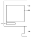
주 표시판부(300M)와 부 표시판부(300S)는 보조 FPC(680S)를 통하여 서로 연결되어 있고, 주 표시판부(300M)의 아래쪽에는 주 FPC(680M)가 부착되어 있으며 주 FPC(680)는 구동 FPC(650)에 부착된다. The
구동 FPC(650)는 또한 인터페이스(interface) FPC라 불리는 것으로, 신호를 전달하기 위한 배선(도시하지 않음)과 그 끝 부분에는 패드(도시하지 않음)가 구비되어 있다. 또한, 구동 FPC(650)의 패드와 접촉하는 주 및 보조 FPC(680M, 680S)와 각 표시판부(300M, 300S)에도 패드가 구비되어 있다.The driving
구동 FPC(650)에는 결합시 부 표시판부(300S)가 위치하는 절개부(690)가 형성되어 있으며, 백라이트부(900)의 광원부(910)에 인가되는 전류를 제어하는 구동 회로부(750)가 구비되어 있다.The driving
구동 FPC(650)의 패드, 주 및 보조 FPC(680M, 680S)의 패드와 각 표시판부(300M, 300S)의 패드를 서로 전기적으로 연결하기 위하여 납땜으로 연결하거나 이방성 도전막(anisotropic conductive film, ACF)을 사용할 수 있다. In order to electrically connect the pads of the driving
다시 도 1을 참조하면, 계조 전압 생성부(800)는 화소의 휘도와 관련된 한 벌 또는 두 벌의 복수 계조 전압을 생성한다. 두 벌이 있는 경우 두 벌 중 한 벌 은 공통 전압(Vcom)에 대하여 양의 값을 가지고 다른 한 벌은 음의 값을 가진다.Referring back to FIG. 1, the
게이트 구동부(400)는 표시판부(300)의 게이트선(G1-Gn)에 연결되어 스위칭 소자(Q)를 턴온시킬 수 있는 게이트 온 전압(Von)과 스위칭 소자(Q)를 턴오프시킬 수 있는 게이트 오프 전압(Voff)의 조합으로 이루어진 게이트 신호를 게이트선(G1-Gn)에 인가한다. The
데이터 구동부(500)는 표시판부(300)의 데이터선(D1-Dm)에 연결되어 계조 전압 생성부(800)로부터의 계조 전압을 선택하여 데이터 신호로서 화소에 인가한다.The
신호 제어부(600)는 게이트 구동부(400) 및 데이터 구동부(500) 등의 동작을 제어한다.The
신호 제어부(600), 게이트 구동부(400), 데이터 구동부(500) 및 계조 전압 생성부(800)는 도 3에 도시한 것처럼 하나의 통합 칩(700)으로 구현되어 COG(chip on glass) 방식으로 주 표시판부(300M)에 장착되어 있다. The
통합 칩(700)은 연결부(660)를 통하여 외부의 MPU(mobile processing unit)(도시하지 않음)로부터 신호를 입력받고 처리한 신호를 FPC(650)에 구비된 배선을 통하여 주 표시판부(300M) 및 부 표시판부(300S)에 공급한다.The
그러면 이러한 액정 표시 장치의 표시 동작에 대하여 상세하게 설명한다.The display operation of such a liquid crystal display device will now be described in detail.
신호 제어부(600)는 외부의 그래픽 제어기(도시하지 않음)로부터 입력 영상 신호(R, G, B) 및 이의 표시를 제어하는 입력 제어 신호, 예를 들면 수직 동기 신 호(Vsync)와 수평 동기 신호(Hsync), 메인 클록(MCLK), 데이터 인에이블 신호(DE) 등을 제공받는다. 신호 제어부(600)는 입력 영상 신호(R, G, B)와 입력 제어 신호를 기초로 영상 신호(R, G, B)를 액정 표시판 조립체(300)의 동작 조건에 맞게 적절히 처리하고 게이트 제어 신호(CONT1) 및 데이터 제어 신호(CONT2) 등을 생성한 후, 게이트 제어 신호(CONT1)를 게이트 구동부(400)로 내보내고 데이터 제어 신호(CONT2)와 처리한 영상 신호(DAT)는 데이터 구동부(500)로 내보낸다.The
게이트 제어 신호(CONT1)는 게이트 온 전압(Von)의 출력 시작을 지시하는 수직 동기 시작 신호(STV), 게이트 온 전압(Von)의 출력 시기를 제어하는 게이트 클록 신호(CPV) 및 게이트 온 전압(Von)의 지속 시간을 한정하는 출력 인에이블 신호(OE) 등을 포함한다.The gate control signal (CONT1) includes a gate-on voltage vertical synchronization start signal (STV) for instructing the start of output of the (V on), the gate-on voltage gated clock signal that controls the output timing of the (V on) (CPV) and the gate-on An output enable signal OE or the like that defines the duration of the voltage V on .
데이터 제어 신호(CONT2)는 영상 데이터(DAT)의 입력 시작을 알리는 수평 동기 시작 신호(STH)와 데이터선(D1-Dm)에 해당 데이터 전압을 인가하라는 로드 신호(LOAD), 공통 전압(Vcom)에 대한 데이터 전압의 극성(이하 "공통 전압에 대한 데이터 전압의 극성"을 줄여 "데이터 전압의 극성"이라 함)을 반전시키는 반전 신호(RVS) 및 데이터 클록 신호(HCLK) 등을 포함한다.The data control signal CONT2 includes a horizontal synchronization start signal STH indicating the start of input of the image data DAT, a load signal LOAD for applying a corresponding data voltage to the data lines D 1 -D m , and a common voltage ( V inverted signal (RVS), data clock signal (HCLK), etc. to invert the polarity of the data voltage for the com (hereinafter referred to as "polarity of the data voltage by reducing the polarity of the data voltage for the common voltage"), etc. do.
데이터 구동부(500)는 신호 제어부(600)로부터의 데이터 제어 신호(CONT2)에 따라 한 행의 화소에 대한 영상 데이터(DAT)를 차례로 입력받아 시프트시키고, 계조 전압 생성부(800)로부터의 계조 전압 중 각 영상 데이터(DAT)에 대응하는 계조 전압을 선택함으로써 영상 데이터(DAT)를 해당 데이터 전압으로 변환한 후, 이를 해당 데이터선(D1-Dm)에 인가한다.The
게이트 구동부(400)는 신호 제어부(600)로부터의 게이트 제어 신호(CONT1)에 따라 게이트 온 전압(Von)을 게이트선(G1-Gn)에 인가하여 이 게이트선(G
1-Gn)에 연결된 스위칭 소자(Q)를 턴온시키며, 이에 따라 데이터선(D1-Dm)에 인가된 데이터 전압이 턴온된 스위칭 소자(Q)를 통하여 해당 화소에 인가된다. The
화소에 인가된 데이터 전압과 공통 전압(Vcom)의 차이는 액정 축전기(CLC)의 충전 전압, 즉 화소 전압으로서 나타난다. 액정 분자들은 화소 전압의 크기에 따라 그 배열을 달리하며, 이에 따라 액정층(3)을 통과하는 빛의 편광이 변화한다. 이러한 편광의 변화는 표시판(100, 200)에 부착된 편광자(도시하지 않음)에 의하여 빛의 투과율 변화로 나타난다.The difference between the data voltage applied to the pixel and the common voltage V com is shown as the charging voltage of the liquid crystal capacitor C LC , that is, the pixel voltage. The arrangement of the liquid crystal molecules varies according to the magnitude of the pixel voltage, thereby changing the polarization of light passing through the
1 수평 주기(또는 "1H")[수평 동기 신호(Hsync), 데이터 인에이블 신호(DE), 게이트 클록(CPV)의 한 주기]가 지나면 데이터 구동부(500)와 게이트 구동부(400)는 다음 행의 화소에 대하여 동일한 동작을 반복한다. 이러한 방식으로, 한 프레임(frame) 동안 모든 게이트선(G1-Gn)에 대하여 차례로 게이트 온 전압(Von)을 인가하여 모든 화소에 데이터 전압을 인가한다. 한 프레임이 끝나면 다음 프레임이 시작되고 각 화소에 인가되는 데이터 전압의 극성이 이전 프레임에서의 극성과 반대가 되도록 데이터 구동부(500)에 인가되는 반전 신호(RVS)의 상태가 제어된다("프 레임 반전"). 이때, 한 프레임 내에서도 반전 신호(RVS)의 특성에 따라 한 데이터선을 통하여 흐르는 데이터 전압의 극성이 바뀌거나(보기: "행 반전", "점 반전"), 한 화소행에 인가되는 데이터 전압의 극성도 서로 다를 수 있다(보기: "열 반전", "점 반전").After one horizontal period (or “1H”) (one period of the horizontal sync signal H sync , the data enable signal DE, and the gate clock CPV), the
그러면 본 발명의 실시예에 따른 액정 표시 장치에 대하여 도 4 내지 도 8을 참고로 하여 상세히 설명한다.Next, a liquid crystal display according to an exemplary embodiment of the present invention will be described in detail with reference to FIGS. 4 to 8.
도 4는 도 3b에 도시한 구동 회로부의 개략도이며, 도 5a 및 도 5b는 도 4에 도시한 축전기와 액정 표시 장치의 여러 실험 조건에 따른 소음을 측정한 결과를 나타낸 표이고, 도 6a 및 도 6b는 본 발명의 한 실시예에 따라 소음을 측정한 그래프이다.FIG. 4 is a schematic view of the driving circuit unit shown in FIG. 3B, and FIGS. 5A and 5B are tables showing results of noise measured according to various experimental conditions of the capacitor and the liquid crystal display shown in FIG. 4, and FIGS. 6A and FIG. 6b is a graph measuring noise according to an embodiment of the present invention.
도 4에는 도 3b에 도시한 구동 회로부(750)와 이에 연결되어 있는 광원부(910), 즉 발광 다이오드를 나타내었다.4 illustrates a driving
도 4에 도시한 바와 같이, 본 발명의 한 실시예에 따른 구동 회로부(750)는 전류 생성부(751)와 전류 설정부(753)를 포함한다.As shown in FIG. 4, the driving
전류 생성부(751)는 집적 회로로 이루어지며 5개의 핀으로 이루어지는 단자, 즉, 제1 및 제2 입력 단자(IN1, IN2), 스위칭 단자(SW), 되먹임 단자(FB) 및 접지 단자(GND)를 포함한다.The
제1 입력 단자(IN1)에는 중소형 표시 장치의 구동에 필요한 직류 전원 전압(VBAT)이 입력되고, 제2 입력 단자(IN2)에는 백라이트부(900)를 동작시키기 위한 인에이블 신호(EN)가 입력된다. 전류 생성부(751)는 스위칭 단자(ST)를 통하여 일 정 주파수로 교류 전류를 발광 다이오드(910)에 출력하며, 되먹임 단자(FB)에는 전류 설정부(753)로부터 되먹임되는 전류가 입력되며, 접지 단자(GND)는 접지 전압에 연결되어 있다.The DC power supply voltage VBAT required for driving the small and medium size display device is input to the first input terminal IN1, and the enable signal EN for operating the
전류 설정부(753)는 복수의 저항(R1-R3), 축전기(C) 및 스위칭 소자(SW)를 포함하며, 디밍 신호(DIM)에 따라 스위칭 소자(SW)의 개폐를 조절함으로써 발광 다이오드(910)에 흐르는 전류의 양을 조절하여 발광 다이오드(910)의 밝기를 조절한다. 특히, 디밍 신호(DIM)가 입력되는 때를 디밍 모드(dimming mode)라 하고, 이러한 디밍 모드에서 발광 다이오드(910)에 흐르는 전류의 양이 점차 감소하면서 어두워진다.The
이때, 도 5a 및 도 5b는 실험 조건을 세 개로 나누고, 각 실험 조건에 대한 세 개의 시료(device under test)에 대하여 소음을 측정한 표로서, 무소음실에서 시료와 3cm 정도의 거리를 두고 마이크로폰을 배치한 후 소음을 측정하였다.5A and 5B are tables for dividing the test conditions into three and measuring noise for three samples (device under test) for each test condition. The microphone is placed at a distance of about 3 cm from the sample in the silent room. After placement the noise was measured.
실험 조건(a, b, c)은 전류 설정부(753)의 축전기(C)의 용량과 액정 표시 장치의 구동 여부로 나누었으며, 모두 디밍 모드이다. 이때, 축전기(C)의 용량이 0인 것은 축전기(C)를 제거한 상태를 의미하고, 구동 여부는 예를 들어, 폴더형 핸드폰에서 핸드폰을 펼친 상태는 구동하는 것에 해당하고 핸드폰을 접은 상태는 구동하지 않는 것에 해당한다.Experimental conditions (a, b, c) were divided into the capacitance of the capacitor (C) of the
시료(#1)는 세 실험 조건(a, b, c)에 대하여 17.3dB, 18.5dB 및 18.7dB를 나타내었고, 시료(#2)는 17.7dB, 17.3dB 및 18.0dB를 나타내었고, 시료(#3)는 17.2dB, 17.3dB 및 17.4dB를 나타내었다.
이때, 소음은 시간 영역에서 측정한 것을 주파수 영역으로 푸리에 변환(Fourier transform)한 것이며, 이렇게 하면 해당 주파수에서의 소음을 좀 더 상세하게 알 수 있다. 도 6a 및 도 6b는 시료(#1)에 대한 실험 결과 중 두 실험 조건(a, c)에 대한 것을 측정한 그래프이며, 나머지 시료(#2, #3)에 대한 것도 이와 동일하게 측정하였다. At this time, the noise is a Fourier transform (Fourier transform) measured in the time domain to the frequency domain, this can be seen in more detail the noise at the frequency. 6A and 6B are graphs of two experimental conditions (a and c) of the experimental results for the sample (# 1), and the same for the remaining samples (# 2 and # 3).
도 6a 및 도 6b에서 데시벨은 20log(y/x)로 측정되고, x는 기준이 되는 음압으로서 20uPa이다. 실험 조건(a)에서 17.3dB이고 실험 조건(c)에서 18.7dB로서 실험 조건(a)의 경우에는 실험 조건(c)보다 1.4dB 적음을 알 수 있다. 이는 실험 조건(c)에서는 5.5KHz의 고조파 성분(harmonic component)에서 골고루 소음이 발생하여 전체적인 소음 레벨을 증가시키지만, 축전기(C)를 제거한 실험 조건(a)에서는 5.409kHz의 고조파 성분이 두 번째 고조파 성분을 제외하고는 급격히 약화되면서 전체적인 소음 레벨을 낮추는 역할을 한다.In FIGS. 6A and 6B, decibels are measured at 20 log (y / x), and x is 20 uPa as a reference sound pressure. It can be seen that the experimental condition (a) is 17.3 dB and the experimental condition (c) is 18.7 dB, which is 1.4 dB less than the experimental condition (c). In experimental condition (c), the noise is evenly generated in the harmonic component of 5.5KHz, which increases the overall noise level, but in experimental condition (a) where capacitor (C) is removed, the harmonic component of 5.409kHz is the second harmonic. Except for the components, it is rapidly weakened and serves to lower the overall noise level.
마찬가지로, 시료(#2, #3)의 경우에도 축전기(C)를 제거한 상태가 소음이 적음을 알 수 있다.Similarly, in the case of
또한, 본 실험에서는 축전기(C)를 제거한 상태에서 실험한 결과를 보여 주었지만, 100nF이하인 경우에도 동일한 결과를 얻었다.In addition, in the present experiment, the results of experiments with the capacitor C removed were shown, but the same results were obtained even when 100 nF or less.
이와 같이, 축전기(C)를 100nF 이하의 용량으로 하면 소음을 상당히 줄일 수 있음을 알 수 있다.Thus, it can be seen that the noise can be significantly reduced by using the capacitor C at a capacity of 100 nF or less.
도 7은 본 발명의 다른 실시예에 따른 공통 전압 생성부(710)의 블록도이다. 본 발명의 다른 실시예에 따른 공통 전압 생성부(710)는 오실레이터(711)와 이에 연결되어 있는 전압 생성부(712)를 포함하고, 오실레이터(711)의 두 단자(OSC1, OSC2) 사이에는 저항(Rf)이 연결되어 있다.7 is a block diagram of a
오실레이터(711)는 오실레이션 신호(OSC)를 내보내고 전압 생성부(713)는 이 신호(OSC)에 따라 공통 전압(Vcom)의 주파수롤 조절한다.The
중소형 액정 표시 장치의 경우에는 대형 액정 표시 장치에 비하여 작은 데이터 전압으로 구동을 하기 위하여 공통 전압(Vcom)도 반전 구동을 하게 되며 일정한 주파수를 갖는다. 이러한 주파수는 통상 프레임 주파수와 게이트선의 수효를 곱한 만큼을 갖는데, 예를 들어 초당 60프레임이고 게이트선의 수효가 160개인 경우에는 9.6kHz이며, 이는 가청 주파수에 포함된다.In the case of the small and medium-sized liquid crystal display, the common voltage Vcom is also inverted and has a constant frequency in order to drive with a smaller data voltage than the large liquid crystal display. This frequency is typically multiplied by the frame frequency multiplied by the number of gate lines, for example 60 frames per second and 160 gate lines, which is 9.6 kHz, which is included in the audible frequency.
다시 도 6a 및 도 6b를 참고하면, 도 6a의 경우에는 10.87kHz에서, 도 6b의 경우에는 11.0kHz에서 소음 레벨이 급격하게 증가하며 이는 공통 전압(Vcom) 주파수 근처에서 소음 레벨이 증가함을 알 수 있다.Referring again to FIGS. 6A and 6B, the noise level increases rapidly at 10.87 kHz in FIG. 6A and at 11.0 kHz in FIG. 6B, indicating that the noise level increases near the common voltage (Vcom) frequency. Can be.
따라서, 공통 전압 주파수를 가청 주파수 대역에서 벗어나게 설계하는 것이 바람직하다. 예를 들어, 20kHz를 초과하도록 설계하는 것이다. 이러한 공통 전압 주파수의 조절은 오실레이터(711)에 연결되어 있는 저항(Rf)의 크기를 조절함으로써 가능하다. 저항(Rf)의 크기와 주파수는 반비례하는 관계에 있는데, 저항(Rf)의 크기를 줄여서 가청 주파수 대역인 20kHz를 넘어서도록 주파수를 증가시킬 수 있다.Therefore, it is desirable to design the common voltage frequency out of the audible frequency band. For example, it is designed to exceed 20kHz. This common voltage frequency can be adjusted by adjusting the size of the resistor Rf connected to the
도 8은 본 발명의 다른 실시예에 따른 액정 표시 장치의 개략도의 측면도로서, 도 3a에 도시한 액정 표시 장치와 백라이트부(900)를 결합한 형태이다.
FIG. 8 is a side view of a schematic view of a liquid crystal display according to another exemplary embodiment, in which the liquid crystal display and the
백라이트부(900)는 도 8을 기준으로 왼쪽에 배치되어 있는 광원부(910)와 도광판을 통하여 두 표시판부(300M, 300S)에 각각 빛을 공급하며, 두 표시판부(300M, 300S)는 백라이트부(900)를 사이에 두고 서로 반대쪽에 서로 위치한다.The
두 표시판부(300M, 300S)는 각각 하부 표시판(100M, 100S)과 상부 표시판(200M, 200S)을 포함하고, 통합 칩(700)은 주 표시판부(300M)의 하부 표시판(100M)에 장착되어 있다.The two
주 및 보조 FPC(680M, 680S)는 접혀서 위쪽으로 올라가고, 보조 FPC(680S)는 주 표시판부(300M)의 하부 표시판(100M)과 부 표시판부(300S)의 하부 표시판(100S) 사이에 연결되어 있고, 주 FPC(680M)는 접힌 상태에서 구동 FPC(650)와 연결된다. 구동 FPC(650)는 백라이트부(900)의 위쪽에 위치하여 절개부(690)에는 부 표시판부(300S)가 들어간다.The primary and
이때, 백라이트부(900)의 위쪽에는 보조 FPC(680S)와 사이에 양면 테이프로 된 절연 부재(950)가 부착되어 있다.At this time, an insulating
이 절연 부재(950)는 백라이트부(900)와 보조 FPC(680S) 사이의 발진을 차단하여 소음을 줄이는 역할을 한다. 앞서 설명한 것처럼, 통합 칩(700)은 주 표시판부(300M)와 부 표시판부(300S)를 모두 구동하는데, 부 표시판부(300S)로 전달되는 데이터 전압, 게이트 전압, 공통 전압 등이 백라이트부(900)의 점멸 주파수, 즉 도 4에서 설명한 전류 생성부(751)에서 생성되는 교류 전류의 주파수와 발진을 일으키게 되면 소음이 발생하는데, 절연 부재(950)는 이러한 발진을 차단하는 역할을 하여 소음을 줄인다.The insulating
이와 같이, 전류 설정부(713)의 축전기(C)의 용량을 100nF 이하로 하거나 공통 전압 주파수를 가청 주파수 범위 밖으로 조절하거나 보조 FPC(750)와 백라이트부(900) 사이에 절연 테이프를 붙임으로써, 핸드폰과 같은 중소형 액정 표시 장치에서 발생하는 소음을 줄일 수 있다.In this manner, the capacitance of the capacitor C of the current setting unit 713 is set to 100 nF or less, the common voltage frequency is adjusted out of the audible frequency range, or an insulating tape is applied between the
이상에서 본 발명의 바람직한 실시예에 대하여 상세하게 설명하였지만 본 발명의 권리범위는 이에 한정되는 것은 아니고 다음의 청구범위에서 정의하고 있는 본 발명의 기본 개념을 이용한 당업자의 여러 변형 및 개량 형태 또한 본 발명의 권리범위에 속하는 것이다.
Although the preferred embodiments of the present invention have been described in detail above, the scope of the present invention is not limited thereto, and various modifications and improvements of those skilled in the art using the basic concepts of the present invention defined in the following claims are also provided. It belongs to the scope of rights.
Claims (25)
Priority Applications (5)
| Application Number | Priority Date | Filing Date | Title |
|---|---|---|---|
| KR1020050000411A KR20060079983A (en) | 2005-01-04 | 2005-01-04 | Liquid crystal display |
| TW094140804A TW200632429A (en) | 2005-01-04 | 2005-11-21 | Liquid crystal display |
| JP2005337859A JP2006189801A (en) | 2005-01-04 | 2005-11-22 | Liquid crystal display |
| US11/323,774 US20060146006A1 (en) | 2005-01-04 | 2005-12-29 | Liquid crystal display |
| CNA2006100003077A CN1801308A (en) | 2005-01-04 | 2006-01-04 | Liquid crystal display |
Applications Claiming Priority (1)
| Application Number | Priority Date | Filing Date | Title |
|---|---|---|---|
| KR1020050000411A KR20060079983A (en) | 2005-01-04 | 2005-01-04 | Liquid crystal display |
Publications (1)
| Publication Number | Publication Date |
|---|---|
| KR20060079983A true KR20060079983A (en) | 2006-07-07 |
Family
ID=36639823
Family Applications (1)
| Application Number | Title | Priority Date | Filing Date |
|---|---|---|---|
| KR1020050000411A Withdrawn KR20060079983A (en) | 2005-01-04 | 2005-01-04 | Liquid crystal display |
Country Status (5)
| Country | Link |
|---|---|
| US (1) | US20060146006A1 (en) |
| JP (1) | JP2006189801A (en) |
| KR (1) | KR20060079983A (en) |
| CN (1) | CN1801308A (en) |
| TW (1) | TW200632429A (en) |
Families Citing this family (5)
| Publication number | Priority date | Publication date | Assignee | Title |
|---|---|---|---|---|
| FR2906396A1 (en) * | 2006-09-26 | 2008-03-28 | Thomson Licensing Sas | ELECTROLUMINESCENT DIODE ELEMENT ASSEMBLY FOR BACKLIGHT DEVICE, BACKLIGHT DEVICE, AND BACKLIGHT SCREEN. |
| KR101410465B1 (en) * | 2007-02-22 | 2014-06-23 | 삼성디스플레이 주식회사 | Backlight device and liquid crystal display device having the same |
| TWI419137B (en) * | 2010-08-19 | 2013-12-11 | Innolux Corp | Liquid crystal display device and driving method thereof |
| KR101730500B1 (en) | 2010-11-25 | 2017-04-27 | 삼성디스플레이 주식회사 | A liquid crystal display apparatus and a method for driving the same |
| KR20140080050A (en) * | 2012-12-20 | 2014-06-30 | 삼성전자주식회사 | Plasma display panel and method for driving thereof |
Family Cites Families (10)
| Publication number | Priority date | Publication date | Assignee | Title |
|---|---|---|---|---|
| JP3286582B2 (en) * | 1997-10-23 | 2002-05-27 | セイコーインスツルメンツ株式会社 | Display device and method of manufacturing display device |
| TW570203U (en) * | 1998-08-03 | 2004-01-01 | Rohm Co Ltd | Liquid crystal display element |
| KR100444694B1 (en) * | 1999-08-04 | 2004-08-18 | 엘지전자 주식회사 | Apparatus For Liquid Crystal Display in A Folder Form Mobile Telecommunication Terminal |
| JP3645770B2 (en) * | 2000-01-28 | 2005-05-11 | 株式会社日立製作所 | Liquid crystal display |
| CN1193261C (en) * | 2001-06-08 | 2005-03-16 | 那纳须株式会社 | Liquid crystal display device and method for manufacturing the same |
| JP2004021238A (en) * | 2002-06-20 | 2004-01-22 | Nec Saitama Ltd | Display device and mobile terminal system |
| US6721022B1 (en) * | 2002-11-14 | 2004-04-13 | Wintek Corporation | Liquid crystal display with electro-luminescent cell having a double-face backlight effect |
| US6864641B2 (en) * | 2003-02-20 | 2005-03-08 | Visteon Global Technologies, Inc. | Method and apparatus for controlling light emitting diodes |
| JP4137712B2 (en) * | 2003-06-17 | 2008-08-20 | アルプス電気株式会社 | Surface light emitting device and liquid crystal display device |
| JP4703955B2 (en) * | 2003-09-10 | 2011-06-15 | 株式会社 日立ディスプレイズ | Display device |
-
2005
- 2005-01-04 KR KR1020050000411A patent/KR20060079983A/en not_active Withdrawn
- 2005-11-21 TW TW094140804A patent/TW200632429A/en unknown
- 2005-11-22 JP JP2005337859A patent/JP2006189801A/en not_active Withdrawn
- 2005-12-29 US US11/323,774 patent/US20060146006A1/en not_active Abandoned
-
2006
- 2006-01-04 CN CNA2006100003077A patent/CN1801308A/en active Pending
Also Published As
| Publication number | Publication date |
|---|---|
| TW200632429A (en) | 2006-09-16 |
| US20060146006A1 (en) | 2006-07-06 |
| JP2006189801A (en) | 2006-07-20 |
| CN1801308A (en) | 2006-07-12 |
Similar Documents
| Publication | Publication Date | Title |
|---|---|---|
| US6943506B2 (en) | Inverter apparatus and liquid crystal display including inverter apparatus | |
| KR20050062852A (en) | Liquid crystal device, driving device and method of light source for display device | |
| KR101129432B1 (en) | Liquid crystal display | |
| KR20060104088A (en) | Circuit board of display device and display device including same | |
| US7205971B2 (en) | Driving circuit of a liquid crystal display device for eliminating residual images | |
| US20060170368A1 (en) | Apparatus and method of driving light source for display device | |
| US20060044828A1 (en) | Display device, driving device of display device, and driving device of light source for display device | |
| JP5255751B2 (en) | Driving device for liquid crystal display device and liquid crystal display device having the same | |
| KR20060079983A (en) | Liquid crystal display | |
| KR20060070346A (en) | Display device | |
| US20080074376A1 (en) | Liquid crystal display and method thereof | |
| JP2006201755A (en) | Dual display device | |
| KR20080019397A (en) | Liquid crystal display | |
| KR100925466B1 (en) | Liquid crystal display | |
| KR20050106689A (en) | Flexible printed circuit film and liquid crystal display including the same | |
| KR20020057225A (en) | Liquid crystal display device and method for driving the same | |
| KR20060029367A (en) | Liquid crystal display | |
| KR20060018390A (en) | Liquid crystal display | |
| KR20060023698A (en) | Display device | |
| KR20080046980A (en) | Liquid crystal display | |
| KR20060077730A (en) | Liquid crystal display | |
| KR20060134371A (en) | Display device and driving device of display device | |
| KR20040077011A (en) | Device of driving liquid crystal display | |
| KR20060070347A (en) | Backlight Device and Display Device | |
| KR20080022874A (en) | Liquid crystal display |
Legal Events
| Date | Code | Title | Description |
|---|---|---|---|
| PA0109 | Patent application |
Patent event code: PA01091R01D Comment text: Patent Application Patent event date: 20050104 |
|
| PG1501 | Laying open of application | ||
| PC1203 | Withdrawal of no request for examination | ||
| WITN | Application deemed withdrawn, e.g. because no request for examination was filed or no examination fee was paid |