KR102819838B1 - Semiconductor devices - Google Patents
Semiconductor devices Download PDFInfo
- Publication number
- KR102819838B1 KR102819838B1 KR1020190140410A KR20190140410A KR102819838B1 KR 102819838 B1 KR102819838 B1 KR 102819838B1 KR 1020190140410 A KR1020190140410 A KR 1020190140410A KR 20190140410 A KR20190140410 A KR 20190140410A KR 102819838 B1 KR102819838 B1 KR 102819838B1
- Authority
- KR
- South Korea
- Prior art keywords
- silicon
- pattern
- semiconductor
- active structure
- substrate
- Prior art date
- Legal status (The legal status is an assumption and is not a legal conclusion. Google has not performed a legal analysis and makes no representation as to the accuracy of the status listed.)
- Active
Links
Images






Classifications
-
- H—ELECTRICITY
- H10—SEMICONDUCTOR DEVICES; ELECTRIC SOLID-STATE DEVICES NOT OTHERWISE PROVIDED FOR
- H10D—INORGANIC ELECTRIC SEMICONDUCTOR DEVICES
- H10D64/00—Electrodes of devices having potential barriers
- H10D64/01—Manufacture or treatment
- H10D64/017—Manufacture or treatment using dummy gates in processes wherein at least parts of the final gates are self-aligned to the dummy gates, i.e. replacement gate processes
-
- H01L21/02532—
-
- H01L21/76811—
-
- H—ELECTRICITY
- H10—SEMICONDUCTOR DEVICES; ELECTRIC SOLID-STATE DEVICES NOT OTHERWISE PROVIDED FOR
- H10D—INORGANIC ELECTRIC SEMICONDUCTOR DEVICES
- H10D30/00—Field-effect transistors [FET]
- H10D30/01—Manufacture or treatment
- H10D30/014—Manufacture or treatment of FETs having zero-dimensional [0D] or one-dimensional [1D] channels, e.g. quantum wire FETs, single-electron transistors [SET] or Coulomb blockade transistors
-
- H—ELECTRICITY
- H10—SEMICONDUCTOR DEVICES; ELECTRIC SOLID-STATE DEVICES NOT OTHERWISE PROVIDED FOR
- H10D—INORGANIC ELECTRIC SEMICONDUCTOR DEVICES
- H10D30/00—Field-effect transistors [FET]
- H10D30/01—Manufacture or treatment
- H10D30/021—Manufacture or treatment of FETs having insulated gates [IGFET]
- H10D30/024—Manufacture or treatment of FETs having insulated gates [IGFET] of fin field-effect transistors [FinFET]
-
- H—ELECTRICITY
- H10—SEMICONDUCTOR DEVICES; ELECTRIC SOLID-STATE DEVICES NOT OTHERWISE PROVIDED FOR
- H10D—INORGANIC ELECTRIC SEMICONDUCTOR DEVICES
- H10D30/00—Field-effect transistors [FET]
- H10D30/40—FETs having zero-dimensional [0D], one-dimensional [1D] or two-dimensional [2D] charge carrier gas channels
- H10D30/43—FETs having zero-dimensional [0D], one-dimensional [1D] or two-dimensional [2D] charge carrier gas channels having one-dimensional [1D] charge carrier gas channels, e.g. quantum wire FETs or transistors having 1D quantum-confined channels
-
- H—ELECTRICITY
- H10—SEMICONDUCTOR DEVICES; ELECTRIC SOLID-STATE DEVICES NOT OTHERWISE PROVIDED FOR
- H10D—INORGANIC ELECTRIC SEMICONDUCTOR DEVICES
- H10D30/00—Field-effect transistors [FET]
- H10D30/60—Insulated-gate field-effect transistors [IGFET]
- H10D30/611—Insulated-gate field-effect transistors [IGFET] having multiple independently-addressable gate electrodes influencing the same channel
-
- H—ELECTRICITY
- H10—SEMICONDUCTOR DEVICES; ELECTRIC SOLID-STATE DEVICES NOT OTHERWISE PROVIDED FOR
- H10D—INORGANIC ELECTRIC SEMICONDUCTOR DEVICES
- H10D30/00—Field-effect transistors [FET]
- H10D30/60—Insulated-gate field-effect transistors [IGFET]
- H10D30/62—Fin field-effect transistors [FinFET]
- H10D30/6215—Fin field-effect transistors [FinFET] having multiple independently-addressable gate electrodes
-
- H—ELECTRICITY
- H10—SEMICONDUCTOR DEVICES; ELECTRIC SOLID-STATE DEVICES NOT OTHERWISE PROVIDED FOR
- H10D—INORGANIC ELECTRIC SEMICONDUCTOR DEVICES
- H10D30/00—Field-effect transistors [FET]
- H10D30/60—Insulated-gate field-effect transistors [IGFET]
- H10D30/67—Thin-film transistors [TFT]
- H10D30/6729—Thin-film transistors [TFT] characterised by the electrodes
- H10D30/673—Thin-film transistors [TFT] characterised by the electrodes characterised by the shapes, relative sizes or dispositions of the gate electrodes
- H10D30/6735—Thin-film transistors [TFT] characterised by the electrodes characterised by the shapes, relative sizes or dispositions of the gate electrodes having gates fully surrounding the channels, e.g. gate-all-around
-
- H—ELECTRICITY
- H10—SEMICONDUCTOR DEVICES; ELECTRIC SOLID-STATE DEVICES NOT OTHERWISE PROVIDED FOR
- H10D—INORGANIC ELECTRIC SEMICONDUCTOR DEVICES
- H10D30/00—Field-effect transistors [FET]
- H10D30/60—Insulated-gate field-effect transistors [IGFET]
- H10D30/67—Thin-film transistors [TFT]
- H10D30/6757—Thin-film transistors [TFT] characterised by the structure of the channel, e.g. transverse or longitudinal shape or doping profile
-
- H—ELECTRICITY
- H10—SEMICONDUCTOR DEVICES; ELECTRIC SOLID-STATE DEVICES NOT OTHERWISE PROVIDED FOR
- H10D—INORGANIC ELECTRIC SEMICONDUCTOR DEVICES
- H10D30/00—Field-effect transistors [FET]
- H10D30/60—Insulated-gate field-effect transistors [IGFET]
- H10D30/751—Insulated-gate field-effect transistors [IGFET] having composition variations in the channel regions
-
- H—ELECTRICITY
- H10—SEMICONDUCTOR DEVICES; ELECTRIC SOLID-STATE DEVICES NOT OTHERWISE PROVIDED FOR
- H10D—INORGANIC ELECTRIC SEMICONDUCTOR DEVICES
- H10D30/00—Field-effect transistors [FET]
- H10D30/60—Insulated-gate field-effect transistors [IGFET]
- H10D30/791—Arrangements for exerting mechanical stress on the crystal lattice of the channel regions
- H10D30/797—Arrangements for exerting mechanical stress on the crystal lattice of the channel regions being in source or drain regions, e.g. SiGe source or drain
-
- H—ELECTRICITY
- H10—SEMICONDUCTOR DEVICES; ELECTRIC SOLID-STATE DEVICES NOT OTHERWISE PROVIDED FOR
- H10D—INORGANIC ELECTRIC SEMICONDUCTOR DEVICES
- H10D62/00—Semiconductor bodies, or regions thereof, of devices having potential barriers
- H10D62/10—Shapes, relative sizes or dispositions of the regions of the semiconductor bodies; Shapes of the semiconductor bodies
- H10D62/117—Shapes of semiconductor bodies
- H10D62/118—Nanostructure semiconductor bodies
- H10D62/119—Nanowire, nanosheet or nanotube semiconductor bodies
- H10D62/121—Nanowire, nanosheet or nanotube semiconductor bodies oriented parallel to substrates
-
- H—ELECTRICITY
- H10—SEMICONDUCTOR DEVICES; ELECTRIC SOLID-STATE DEVICES NOT OTHERWISE PROVIDED FOR
- H10D—INORGANIC ELECTRIC SEMICONDUCTOR DEVICES
- H10D62/00—Semiconductor bodies, or regions thereof, of devices having potential barriers
- H10D62/10—Shapes, relative sizes or dispositions of the regions of the semiconductor bodies; Shapes of the semiconductor bodies
- H10D62/17—Semiconductor regions connected to electrodes not carrying current to be rectified, amplified or switched, e.g. channel regions
- H10D62/213—Channel regions of field-effect devices
- H10D62/221—Channel regions of field-effect devices of FETs
- H10D62/235—Channel regions of field-effect devices of FETs of IGFETs
- H10D62/299—Channel regions of field-effect devices of FETs of IGFETs having lateral doping variations
-
- H—ELECTRICITY
- H10—SEMICONDUCTOR DEVICES; ELECTRIC SOLID-STATE DEVICES NOT OTHERWISE PROVIDED FOR
- H10D—INORGANIC ELECTRIC SEMICONDUCTOR DEVICES
- H10D62/00—Semiconductor bodies, or regions thereof, of devices having potential barriers
- H10D62/80—Semiconductor bodies, or regions thereof, of devices having potential barriers characterised by the materials
- H10D62/83—Semiconductor bodies, or regions thereof, of devices having potential barriers characterised by the materials being Group IV materials, e.g. B-doped Si or undoped Ge
-
- H—ELECTRICITY
- H10—SEMICONDUCTOR DEVICES; ELECTRIC SOLID-STATE DEVICES NOT OTHERWISE PROVIDED FOR
- H10D—INORGANIC ELECTRIC SEMICONDUCTOR DEVICES
- H10D64/00—Electrodes of devices having potential barriers
- H10D64/01—Manufacture or treatment
-
- H—ELECTRICITY
- H10—SEMICONDUCTOR DEVICES; ELECTRIC SOLID-STATE DEVICES NOT OTHERWISE PROVIDED FOR
- H10D—INORGANIC ELECTRIC SEMICONDUCTOR DEVICES
- H10D84/00—Integrated devices formed in or on semiconductor substrates that comprise only semiconducting layers, e.g. on Si wafers or on GaAs-on-Si wafers
- H10D84/80—Integrated devices formed in or on semiconductor substrates that comprise only semiconducting layers, e.g. on Si wafers or on GaAs-on-Si wafers characterised by the integration of at least one component covered by groups H10D12/00 or H10D30/00, e.g. integration of IGFETs
- H10D84/82—Integrated devices formed in or on semiconductor substrates that comprise only semiconducting layers, e.g. on Si wafers or on GaAs-on-Si wafers characterised by the integration of at least one component covered by groups H10D12/00 or H10D30/00, e.g. integration of IGFETs of only field-effect components
- H10D84/83—Integrated devices formed in or on semiconductor substrates that comprise only semiconducting layers, e.g. on Si wafers or on GaAs-on-Si wafers characterised by the integration of at least one component covered by groups H10D12/00 or H10D30/00, e.g. integration of IGFETs of only field-effect components of only insulated-gate FETs [IGFET]
- H10D84/8311—Integrated devices formed in or on semiconductor substrates that comprise only semiconducting layers, e.g. on Si wafers or on GaAs-on-Si wafers characterised by the integration of at least one component covered by groups H10D12/00 or H10D30/00, e.g. integration of IGFETs of only field-effect components of only insulated-gate FETs [IGFET] the IGFETs characterised by having different channel structures
-
- H—ELECTRICITY
- H10—SEMICONDUCTOR DEVICES; ELECTRIC SOLID-STATE DEVICES NOT OTHERWISE PROVIDED FOR
- H10P—GENERIC PROCESSES OR APPARATUS FOR THE MANUFACTURE OR TREATMENT OF DEVICES COVERED BY CLASS H10
- H10P14/00—Formation of materials, e.g. in the shape of layers or pillars
- H10P14/20—Formation of materials, e.g. in the shape of layers or pillars of semiconductor materials
- H10P14/34—Deposited materials, e.g. layers
- H10P14/3402—Deposited materials, e.g. layers characterised by the chemical composition
- H10P14/3404—Deposited materials, e.g. layers characterised by the chemical composition being Group IVA materials
- H10P14/3411—Silicon, silicon germanium or germanium
-
- H—ELECTRICITY
- H10—SEMICONDUCTOR DEVICES; ELECTRIC SOLID-STATE DEVICES NOT OTHERWISE PROVIDED FOR
- H10W—GENERIC PACKAGES, INTERCONNECTIONS, CONNECTORS OR OTHER CONSTRUCTIONAL DETAILS OF DEVICES COVERED BY CLASS H10
- H10W20/00—Interconnections in chips, wafers or substrates
- H10W20/01—Manufacture or treatment
- H10W20/071—Manufacture or treatment of dielectric parts thereof
- H10W20/081—Manufacture or treatment of dielectric parts thereof by forming openings in the dielectric parts
- H10W20/084—Manufacture or treatment of dielectric parts thereof by forming openings in the dielectric parts for dual-damascene structures
- H10W20/087—Manufacture or treatment of dielectric parts thereof by forming openings in the dielectric parts for dual-damascene structures involving multiple stacked pre-patterned masks
-
- B—PERFORMING OPERATIONS; TRANSPORTING
- B82—NANOTECHNOLOGY
- B82Y—SPECIFIC USES OR APPLICATIONS OF NANOSTRUCTURES; MEASUREMENT OR ANALYSIS OF NANOSTRUCTURES; MANUFACTURE OR TREATMENT OF NANOSTRUCTURES
- B82Y10/00—Nanotechnology for information processing, storage or transmission, e.g. quantum computing or single electron logic
-
- H—ELECTRICITY
- H10—SEMICONDUCTOR DEVICES; ELECTRIC SOLID-STATE DEVICES NOT OTHERWISE PROVIDED FOR
- H10D—INORGANIC ELECTRIC SEMICONDUCTOR DEVICES
- H10D62/00—Semiconductor bodies, or regions thereof, of devices having potential barriers
- H10D62/80—Semiconductor bodies, or regions thereof, of devices having potential barriers characterised by the materials
- H10D62/82—Heterojunctions
- H10D62/822—Heterojunctions comprising only Group IV materials heterojunctions, e.g. Si/Ge heterojunctions
-
- H—ELECTRICITY
- H10—SEMICONDUCTOR DEVICES; ELECTRIC SOLID-STATE DEVICES NOT OTHERWISE PROVIDED FOR
- H10D—INORGANIC ELECTRIC SEMICONDUCTOR DEVICES
- H10D62/00—Semiconductor bodies, or regions thereof, of devices having potential barriers
- H10D62/80—Semiconductor bodies, or regions thereof, of devices having potential barriers characterised by the materials
- H10D62/83—Semiconductor bodies, or regions thereof, of devices having potential barriers characterised by the materials being Group IV materials, e.g. B-doped Si or undoped Ge
- H10D62/832—Semiconductor bodies, or regions thereof, of devices having potential barriers characterised by the materials being Group IV materials, e.g. B-doped Si or undoped Ge being Group IV materials comprising two or more elements, e.g. SiGe
-
- H—ELECTRICITY
- H10—SEMICONDUCTOR DEVICES; ELECTRIC SOLID-STATE DEVICES NOT OTHERWISE PROVIDED FOR
- H10P—GENERIC PROCESSES OR APPARATUS FOR THE MANUFACTURE OR TREATMENT OF DEVICES COVERED BY CLASS H10
- H10P30/00—Ion implantation into wafers, substrates or parts of devices
- H10P30/20—Ion implantation into wafers, substrates or parts of devices into semiconductor materials, e.g. for doping
- H10P30/202—Ion implantation into wafers, substrates or parts of devices into semiconductor materials, e.g. for doping characterised by the semiconductor materials
- H10P30/204—Ion implantation into wafers, substrates or parts of devices into semiconductor materials, e.g. for doping characterised by the semiconductor materials into Group IV semiconductors
-
- H—ELECTRICITY
- H10—SEMICONDUCTOR DEVICES; ELECTRIC SOLID-STATE DEVICES NOT OTHERWISE PROVIDED FOR
- H10P—GENERIC PROCESSES OR APPARATUS FOR THE MANUFACTURE OR TREATMENT OF DEVICES COVERED BY CLASS H10
- H10P30/00—Ion implantation into wafers, substrates or parts of devices
- H10P30/20—Ion implantation into wafers, substrates or parts of devices into semiconductor materials, e.g. for doping
- H10P30/208—Ion implantation into wafers, substrates or parts of devices into semiconductor materials, e.g. for doping of electrically inactive species
Landscapes
- Insulated Gate Type Field-Effect Transistor (AREA)
Abstract
반도체 소자는, 기판 상에, 상기 기판 표면에 수직한 수직 방향으로 교대로 반복 적층되는 실리콘 게르마늄 패턴들 및 실리콘 패턴들을 포함하는 액티브 구조물이 구비된다. 상기 액티브 구조물의 표면 및 기판 상에 구비되고, 상기 기판 표면에 수평한 제2 방향으로 연장되는 게이트 구조물이 구비된다. 상기 액티브 구조물에서 상기 제2 방향과 수직한 제1 방향의 양 측벽 상에 형성되고, 소오스/드레인 영역으로 제공되는 반도체막이 포함된다. 상기 실리콘 게르마늄 패턴들은 실리콘이 도핑된 실리콘 리치 실리콘 게르마늄을 포함한다. 상기 반도체 소자는 우수한 특성을 가질 수 있다. A semiconductor device comprises an active structure including silicon germanium patterns and silicon patterns that are alternately and repeatedly stacked in a vertical direction perpendicular to a surface of the substrate on a substrate. A gate structure is provided on a surface of the active structure and the substrate, and extends in a second direction parallel to the surface of the substrate. A semiconductor film is included that is formed on both sidewalls of the active structure in a first direction perpendicular to the second direction and serves as a source/drain region. The silicon germanium patterns include silicon-rich silicon germanium doped with silicon. The semiconductor device can have excellent characteristics.
Description
본 발명은 반도체 소자 및 그 제조 방법에 관한 것이다. 보다 상세하게, 본 발명은 액티브 핀 구조물을 포함하는 반도체 소자 및 그 제조 방법에 관한 것이다.The present invention relates to a semiconductor device and a method for manufacturing the same. More specifically, the present invention relates to a semiconductor device including an active fin structure and a method for manufacturing the same.
반도체 소자에서, 서로 다른 반도체 물질이 교차하여 반복 적층된 액티브 핀 구조물 상에 핀 전계 효과 트랜지스터가 형성될 수 있다. 상기 핀 전계 효과 트랜지스터는 상기 액티브 핀 구조물에서 전자가 이동할 수 있는 부위가 제한되므로, 상기 핀 전계 효과 트랜지스터의 온 전류가 감소될 수 있다. In a semiconductor device, a fin field effect transistor can be formed on an active fin structure in which different semiconductor materials are alternately and repeatedly laminated. Since the area where electrons can move in the active fin structure is limited in the fin field effect transistor, the on-state current of the fin field effect transistor can be reduced.
본 발명의 일 과제는 우수한 특성을 갖는 반도체 소자를 제공하는데 있다.An object of the present invention is to provide a semiconductor device having excellent characteristics.
상기 본 발명의 일 과제를 달성하기 위한 예시적인 실시예들에 따른 반도체 소자는, 기판 상에, 상기 기판 표면에 수직한 수직 방향으로 교대로 반복 적층되는 실리콘 게르마늄 패턴들 및 실리콘 패턴들을 포함하는 액티브 구조물이 구비된다. 상기 액티브 구조물의 표면 및 기판 상에 구비되고, 상기 기판 표면에 수평한 제2 방향으로 연장되는 게이트 구조물이 구비된다. 상기 액티브 구조물에서 상기 제2 방향과 수직한 제1 방향의 양 측벽 상에 형성되고, 소오스/드레인 영역으로 제공되는 반도체막이 포함된다. 상기 실리콘 게르마늄 패턴들은 실리콘이 도핑된 실리콘 리치 실리콘 게르마늄을 포함한다.According to exemplary embodiments for achieving the above object of the present invention, a semiconductor device comprises an active structure including silicon germanium patterns and silicon patterns that are alternately and repeatedly stacked in a vertical direction perpendicular to a surface of the substrate on a substrate. A gate structure is provided on a surface of the active structure and the substrate, and extends in a second direction parallel to the surface of the substrate. A semiconductor film is included that is formed on both sidewalls of the active structure in a first direction perpendicular to the second direction and serves as a source/drain region. The silicon germanium patterns include silicon-rich silicon germanium doped with silicon.
상기 본 발명의 일 과제를 달성하기 위한 예시적인 실시예들에 따른 반도체 소자는, 기판 상에, 상기 기판 표면에 수직한 수직 방향으로 교대로 반복 적층되는 실리콘 게르마늄 패턴들 및 실리콘 패턴들을 포함하는 액티브 구조물이 구비된다. 상기 액티브 구조물의 상부면 및 상기 액티브 구조물에서 상기 기판 표면에 수평한 제2 방향의 양 측벽 상에 형성되고, 상기 제2 방향으로 연장되는 게이트 구조물이 구비된다. 상기 액티브 구조물에서 상기 제2 방향과 수직한 제1 방향의 양 측벽 상에 구비되고, 상기 게이트 구조물의 상기 제1 방향 양 측에 배치되고, 소오스/드레인 영역으로 제공되는 반도체막이 포함된다. 상기 실리콘 게르마늄 패턴들은 실리콘이 도핑된 실리콘 리치 실리콘 게르마늄을 포함하고, 상기 실리콘 게르마늄 패턴 내의 실리콘 농도는 70% 내지 85%일 수 있다. According to exemplary embodiments for achieving the above object of the present invention, a semiconductor device comprises an active structure including silicon germanium patterns and silicon patterns that are alternately and repeatedly stacked in a vertical direction perpendicular to a surface of the substrate on a substrate. A gate structure is formed on an upper surface of the active structure and on both sidewalls of the active structure in a second direction parallel to the surface of the substrate and extending in the second direction. A semiconductor film is included that is provided on both sidewalls of the active structure in a first direction perpendicular to the second direction, is arranged on both sides of the gate structure in the first direction, and serves as a source/drain region. The silicon germanium patterns include silicon-rich silicon germanium doped with silicon, and a silicon concentration in the silicon germanium pattern may be 70% to 85%.
상기 본 발명의 일 과제를 달성하기 위한 예시적인 실시예들에 따른 반도체 소자는, 기판의 제1 영역 상에 구비되고, 상기 기판 표면에 수직한 수직 방향으로 서로 이격되면서 배치되는 실리콘 패턴들을 포함하는 제1 액티브 구조물이 구비된다. 상기 제1 액티브 구조물의 실리콘 패턴들의 수직 방향의 사이의 갭을 채우면서, 상기 기판 및 제1 액티브 구조물 상에 구비되는 제1 게이트 구조물이 구비된다. 상기 기판의 제2 영역 상에, 상기 수직 방향으로 교대로 반복 적층되는 실리콘 게르마늄 패턴들 및 실리콘 패턴들을 포함하는 제2 액티브 구조물이 구비된다. 상기 제2 액티브 구조물의 표면 및 기판 상에 제2 게이트 구조물이 구비된다. 상기 제2 액티브 구조물의 상기 실리콘 게르마늄 패턴들은 실리콘이 도핑된 실리콘 리치 실리콘 게르마늄을 포함할 수 있다.According to exemplary embodiments of the present invention for achieving the above object, a semiconductor device comprises: a first active structure provided on a first region of a substrate and including silicon patterns spaced apart from each other in a vertical direction perpendicular to a surface of the substrate; a first gate structure provided on the substrate and the first active structure while filling a gap between the silicon patterns of the first active structure in a vertical direction; a second active structure comprising silicon germanium patterns and silicon patterns alternately and repeatedly stacked in the vertical direction is provided on a second region of the substrate; a second gate structure is provided on a surface of the second active structure and the substrate. The silicon germanium patterns of the second active structure may include silicon-rich silicon germanium doped with silicon.
예시적인 실시예들에 따른 반도체 소자는 실리콘 패턴 및 실리콘 게르마늄 패턴이 반복 적층되는 액티브 핀 구조물이 포함되고, 상기 실리콘 게르마늄 패턴은 실리콘이 도핑된 실리콘 리치 실리콘 게르마늄을 포함할 수 있다. 즉, 상기 실리콘 게르마늄 패턴의 실리콘 농도가 증가되어, 상기 실리콘 패턴 및 실리콘 게르마늄 패턴 간의 포텐셜 장벽이 감소되어 포텐셜 웰이 낮아지거나 또는 포텐셜 웰의 경사가 완만해질 수 있다. 따라서, 상기 액티브 핀 구조물에서 전자가 이동할 수 있는 부위가 증가되어 트랜지스터의 온 전류가 증가될 수 있다. According to exemplary embodiments, a semiconductor device includes an active fin structure in which a silicon pattern and a silicon germanium pattern are repeatedly stacked, and the silicon germanium pattern may include silicon-rich silicon germanium doped with silicon. That is, a silicon concentration of the silicon germanium pattern may increase, so that a potential barrier between the silicon pattern and the silicon germanium pattern may decrease, thereby lowering a potential well or making a slope of the potential well gentle. Accordingly, a portion in the active fin structure through which electrons can move may increase, so that an on-state current of the transistor may increase.
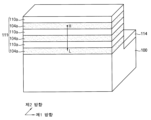
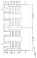
도 1a, 1b, 2 및 3은 예시적인 실시예들에 따른 반도체 소자를 설명하기 위한 단면도, 사시도 및 평면도이다.
도 4는 제1 및 제2 반도체 패턴의 에너지 밴드를 나타낸다.
도 5 내지 도 8은 각각 액티브 구조물의 제1 반도체 패턴들에서 실리콘 농도를 나타내기 위한 사시도들이다.
도 9 내지 도 19는 예시적인 실시예들에 따른 반도체 소자의 제조 방법을 설명하기 위한 단면도들, 평면도들 및 사시도들이다.
도 20 및 도 21은 예시적인 실시예들에 따른 반도체 소자를 설명하기 위한 단면도 및 사시도이다.
도 22 및 도 23은 각각 액티브 구조물의 예비 제1 반도체 패턴들에서 실리콘 농도를 나타내기 위한 사시도들이다.
도 24는 예시적인 실시예들에 따른 반도체 소자를 설명하기 위한 단면도이다.
도 25 내지 도 28은 예시적인 실시예들에 따른 반도체 소자의 제조 방법을 설명하기 위한 단면도들이다.
도 29는 예시적인 실시예들에 따른 반도체 소자를 설명하기 위한 단면도이다.
도 30 및 도 31은 예시적인 실시예들에 따른 반도체 소자의 제조 방법을 설명하기 사시도들이다.
도 32 및 도 33은 예시적인 실시예들에 따른 반도체 소자의 제조 방법을 설명하기 단면도 및 사시도이다.FIGS. 1A, 1B, 2, and 3 are cross-sectional, perspective, and plan views illustrating semiconductor devices according to exemplary embodiments.
Figure 4 shows the energy bands of the first and second semiconductor patterns.
FIGS. 5 to 8 are perspective views each showing the silicon concentration in the first semiconductor patterns of the active structure.
FIGS. 9 to 19 are cross-sectional views, plan views, and perspective views for explaining a method of manufacturing a semiconductor device according to exemplary embodiments.
FIGS. 20 and 21 are cross-sectional and perspective views illustrating semiconductor devices according to exemplary embodiments.
Figures 22 and 23 are perspective views each showing the silicon concentration in preliminary first semiconductor patterns of the active structure.
FIG. 24 is a cross-sectional view illustrating a semiconductor device according to exemplary embodiments.
FIGS. 25 to 28 are cross-sectional views illustrating a method for manufacturing a semiconductor device according to exemplary embodiments.
FIG. 29 is a cross-sectional view illustrating a semiconductor device according to exemplary embodiments.
FIGS. 30 and 31 are perspective views illustrating a method of manufacturing a semiconductor device according to exemplary embodiments.
FIGS. 32 and 33 are cross-sectional and perspective views illustrating a method of manufacturing a semiconductor device according to exemplary embodiments.
도 1a, 1b, 2 및 3은 예시적인 실시예들에 따른 반도체 소자를 설명하기 위한 단면도, 사시도 및 평면도이다. 도 4는 제1 및 제2 반도체 패턴의 에너지 밴드를 나타낸다. 도 5 내지 도 8은 각각 액티브 구조물의 제1 반도체 패턴들에서 실리콘 농도를 나타내기 위한 사시도들이다. FIGS. 1A, 1B, 2, and 3 are cross-sectional, perspective, and plan views, respectively, illustrating semiconductor devices according to exemplary embodiments. FIG. 4 illustrates energy bands of first and second semiconductor patterns. FIGS. 5 to 8 are perspective views each illustrating silicon concentrations in first semiconductor patterns of an active structure.
이하에서는 기판 상면에 평행하고 서로 교차하는 두 방향들을 각각 제1 및 제2 방향들로 정의하고, 기판 상면에 수직한 방향을 수직 방향으로 정의한다. 예시적인 실시예들에 있어서, 상기 제1 및 제2 방향들은 서로 직교할 수 있다.Hereinafter, two directions that are parallel to and intersect the upper surface of the substrate are defined as the first and second directions, respectively, and the direction that is perpendicular to the upper surface of the substrate is defined as the vertical direction. In exemplary embodiments, the first and second directions may be orthogonal to each other.
도 1a는 액티브 구조물 부위를 제1 방향으로 절단한 단면도이다. 도 1b는 액티브 구조물 부위를 제1 방향으로 절단한 단면도이다. 도 1a, 1b, 2 및 3을 참조하면, 상기 반도체 소자는 기판(100) 상에 형성된 액티브 구조물(112), 게이트 구조물(146), 제3 반도체막(134), 절연막(136)을 포함할 수 있다. 또한, 상기 반도체 소자는 소자 분리 패턴(114) 및 스페이서(130)를 더 포함할 수 있다.FIG. 1a is a cross-sectional view of an active structure portion cut in a first direction. FIG. 1b is a cross-sectional view of an active structure portion cut in a first direction. Referring to FIGS. 1a, 1b, 2, and 3, the semiconductor device may include an active structure (112), a gate structure (146), a third semiconductor film (134), and an insulating film (136) formed on a substrate (100). In addition, the semiconductor device may further include a device isolation pattern (114) and a spacer (130).
기판(100)은 실리콘, 게르마늄, 실리콘-게르마늄과 같은 반도체 물질, 또는 GaAs, AlGaAs, InAs, InGaAs 등과 같은 Ⅲ-Ⅴ족 화합물을 포함할 수 있다. The substrate (100) may include a semiconductor material such as silicon, germanium, silicon-germanium, or a group III-V compound such as GaAs, AlGaAs, InAs, InGaAs, etc.
상기 기판(100)에는 상기 제1 방향으로 연장되는 트렌치가 구비되고, 상기 트렌치 내부에는 소자 분리 패턴(114)이 구비될 수 있다. 상기 소자 분리 패턴(114) 부위는 필드 영역으로 제공되고, 상기 소자 분리 패턴들(114) 사이에 형성되는 기판(100) 부위는 액티브 영역으로 제공될 수 있다. 상기 소자 분리 패턴(114)은 예를 들어, 실리콘 산화물과 같은 산화물을 포함할 수 있다.The substrate (100) may be provided with a trench extending in the first direction, and a device isolation pattern (114) may be provided inside the trench. A portion of the device isolation pattern (114) may be provided as a field region, and a portion of the substrate (100) formed between the device isolation patterns (114) may be provided as an active region. The device isolation pattern (114) may include, for example, an oxide such as silicon oxide.
상기 액티브 구조물(112)은 교대로 반복적으로 적층된 제1 반도체 패턴(104b) 및 제2 반도체 패턴(110b)을 포함할 수 있다. 상기 액티브 구조물(112)은 필러(pillar) 형상을 가질 수 있고, 상기 액티브 구조물들(112)은 상기 제1 및 제2 방향으로 서로 이격될 수 있다. 또한, 상기 액티브 구조물들(112)은 상기 제1 및 제2 방향으로 나란하게 배치될 수 있다. The active structure (112) may include a first semiconductor pattern (104b) and a second semiconductor pattern (110b) that are alternately and repeatedly stacked. The active structure (112) may have a pillar shape, and the active structures (112) may be spaced apart from each other in the first and second directions. In addition, the active structures (112) may be arranged in parallel in the first and second directions.
상기 제1 반도체 패턴(104b)은 상기 제2 반도체 패턴(110b)과 다른 물질을 포함할 수 있다. 예를들어, 상기 제1 반도체 패턴(104b)은 상기 기판(100) 및 제2 반도체 패턴(110b)에 대해 높은 식각 선택비를 갖는 물질을 포함할 수 있다. The first semiconductor pattern (104b) may include a different material from the second semiconductor pattern (110b). For example, the first semiconductor pattern (104b) may include a material having a high etching selectivity with respect to the substrate (100) and the second semiconductor pattern (110b).
예시적인 실시예에서, 상기 제1 반도체 패턴(104b)은 실리콘이 도핑된 실리콘 게르마늄일 수 있다. 따라서, 상기 제1 반도체 패턴(104b)은 실리콘 리치 실리콘 게르마늄일 수 있다. 예시적인 실시예에서, 상기 제1 반도체 패턴에서 실리콘의 농도는 70% 이상일 수 있다. 예를들어, 상기 제1 반도체 패턴(104b)에서, 실리콘의 농도는 약 70% 내지 85% 내지 이고, 게르마늄의 농도는 약 15% 내지 30%일 수 있다. 상기 제2 반도체 패턴(110b)은 실리콘을 포함할 수 있다. 예를들어, 상기 제2 반도체 패턴(110b)은 단결정 실리콘일 수 있다. 이하에서는, 상기 제1 반도체 패턴(104b)은 실리콘 게르마늄 패턴으로 칭하고, 상기 제2 반도체 패턴(110b)은 실리콘 패턴으로 칭하면서 설명한다. In an exemplary embodiment, the first semiconductor pattern (104b) may be silicon germanium doped with silicon. Accordingly, the first semiconductor pattern (104b) may be silicon-rich silicon germanium. In an exemplary embodiment, the concentration of silicon in the first semiconductor pattern may be 70% or more. For example, in the first semiconductor pattern (104b), the concentration of silicon may be about 70% to 85%, and the concentration of germanium may be about 15% to 30%. The second semiconductor pattern (110b) may include silicon. For example, the second semiconductor pattern (110b) may be single crystal silicon. Hereinafter, the first semiconductor pattern (104b) will be referred to as a silicon germanium pattern, and the second semiconductor pattern (110b) will be referred to as a silicon pattern.
예시적인 실시예에서, 상기 액티브 구조물(112) 내의 실리콘 게르마늄 패턴들(104b)의 위치에 따라 실리콘의 농도가 다를 수 있다. 일 예로, 상기 액티브 구조물(112) 내의 실리콘 게르마늄 패턴들(104b)에서, 최상부에 형성되는 실리콘 게르마늄 패턴들(104b)에 실리콘의 농도가 가장 높을 수 있다. 또한, 상기 액티브 구조물(112)의 상부로부터 하부로 갈수록 상기 실리콘 게르마늄 패턴들(104b) 내의 실리콘의 농도가 점진적으로 감소될 수 있다. 즉, 도 5에 도시된 것과 같이, 상기 액티브 구조물(112)에서 상기 실리콘 게르마늄 패턴들(104b) 내의 실리콘 농도는 상기 기판(100) 표면으로부터 수직한 방향으로 하방으로 갈수록 점진적으로 감소될 수 있다. In an exemplary embodiment, the concentration of silicon may vary depending on the location of the silicon germanium patterns (104b) within the active structure (112). For example, among the silicon germanium patterns (104b) within the active structure (112), the silicon concentration may be highest in the silicon germanium patterns (104b) formed at the uppermost portion. In addition, the concentration of silicon within the silicon germanium patterns (104b) may gradually decrease from the top to the bottom of the active structure (112). That is, as illustrated in FIG. 5, the silicon concentration within the silicon germanium patterns (104b) in the active structure (112) may gradually decrease downward in a direction perpendicular to the surface of the substrate (100).
일반적으로, 핀 전계효과 트랜지스터에서, 액티브 핀의 하부보다 상부에서 온 전류가 가장 많이 흐른다. 때문에, 상기 액티브 구조물(112)의 최상부에 형성되는 실리콘 게르마늄 패턴들(104b(T))에서 실리콘의 농도를 크게 증가시킴으로써 핀 전계효과 트랜지스터의 온 전류가 증가되는 효과를 크게 할 수 있다. In general, in a fin field-effect transistor, the on-state current flows most from the upper part of the active fin than from the lower part. Therefore, by significantly increasing the concentration of silicon in the silicon germanium patterns (104b(T)) formed at the uppermost part of the active structure (112), the effect of increasing the on-state current of the fin field-effect transistor can be greatly enhanced.
예시적인 실시예에서, 상기 액티브 구조물(112) 에서 각 실리콘 게르마늄 패턴들(104b) 내의 위치별로 실리콘의 농도가 다를 수 있다. In an exemplary embodiment, the concentration of silicon may vary at different locations within each of the silicon germanium patterns (104b) in the active structure (112).
일 예로, 도 6에 도시된 것과 같이, 상기 각 실리콘 게르마늄 패턴들 (104b)에서 제1 방향의 양 측벽 부위에서 실리콘의 농도가 가장 높고, 상기 제1 방향의 양 측벽으로부터 중심 부위로 갈수록 실리콘의 농도가 점진적으로 감소될 수 있다.For example, as illustrated in FIG. 6, in each of the silicon germanium patterns (104b), the silicon concentration may be highest at both sidewall portions in the first direction, and the silicon concentration may gradually decrease from the both sidewalls in the first direction toward the center portion.
일 예로, 도 7에 도시된 것과 같이, 상기 각 실리콘 게르마늄 패턴들 (104b)에서 제2 방향의 양 측벽 부위에서 실리콘의 농도가 가장 높고, 상기 제2 방향의 양 측벽으로부터 중심 부위로 갈수록 실리콘의 농도가 점진적으로 감소될 수 있다.For example, as illustrated in FIG. 7, in each of the silicon germanium patterns (104b), the silicon concentration may be highest at both sidewall portions in the second direction, and the silicon concentration may gradually decrease from the both sidewalls in the second direction toward the center portion.
일 예로, 도 8에 도시된 것과 같이, 상기 각 실리콘 게르마늄 패턴들 (104b)에서 제1 방향의 양 측벽 부위 및 제2 방향의 양 측벽 부위에서 실리콘의 농도가 가장 높고, 각 실리콘 게르마늄 패턴들(104a)의 상기 제1 및 제2 방향의 측벽 부위로부터 중심 부위로 갈수록 실리콘의 농도가 점진적으로 감소될 수 있다.For example, as illustrated in FIG. 8, in each of the silicon germanium patterns (104b), the silicon concentration is highest at both sidewall portions in the first direction and both sidewall portions in the second direction, and the silicon concentration may gradually decrease from the sidewall portions in the first and second directions of each of the silicon germanium patterns (104a) toward the center portion.
일부 예시적인 실시예에서, 상기 실리콘 게르마늄 패턴들(104b)에 도핑된 실리콘의 농도는 상기 실리콘 게르마늄 패턴들(104b)의 수직 방향 위치 및 상기 각 실리콘 게르마늄 패턴들 내의 위치별로 균일할 수도 있다. In some exemplary embodiments, the concentration of silicon doped in the silicon germanium patterns (104b) may be uniform with respect to the vertical position of the silicon germanium patterns (104b) and with respect to the position within each of the silicon germanium patterns.
상기 액티브 구조물(112)은 핀 전계효과 트랜지스터의 채널 영역으로 제공될 수 있다. The above active structure (112) can be provided as a channel region of a fin field effect transistor.
상기 게이트 구조물(146)은 상기 액티브 구조물(112)의 제2 방향의 양 측벽과 상부면 및 상기 기판(100) 상에 형성될 수 있다. 상기 게이트 구조물(146)은 상기 제2 방향으로 연장될 수 있다. 따라서, 상기 게이트 구조물(146)은 상기 제2 방향으로 배치되는 액티브 구조물들(112)의 제2 방향의 양 측벽 및 상부면을 덮을 수 있다. 상기 게이트 구조물(146)의 상부면은 상기 액티브 구조물(112)의 상부면보다 더 높을 수 있다. The gate structure (146) may be formed on both side walls and an upper surface of the active structure (112) in the second direction and on the substrate (100). The gate structure (146) may extend in the second direction. Therefore, the gate structure (146) may cover both side walls and an upper surface of the active structures (112) arranged in the second direction in the second direction. The upper surface of the gate structure (146) may be higher than the upper surface of the active structure (112).
상기 게이트 구조물(146)의 측벽 상에는 상기 스페이서(130)가 구비될 수 있다. 상기 스페이서(130)는 예를들어, 실리콘 질화물을 포함할 수 있다. The spacer (130) may be provided on the side wall of the gate structure (146). The spacer (130) may include, for example, silicon nitride.
상기 게이트 구조물(146)은 게이트 절연막 패턴(140), 게이트 패턴(142) 및 하드 마스크(144)를 포함할 수 있다. The above gate structure (146) may include a gate insulating film pattern (140), a gate pattern (142), and a hard mask (144).
상기 게이트 절연막 패턴(140)은 상기 액티브 구조물(112)의 제2 방향의 양 측벽과 상부면을 덮으면서 컨포멀하게 형성될 수 있다. 또한, 상기 게이트 절연막 패턴(140)은 상기 스페이서(130)의 내측벽에 형성될 수 있다. 따라서, 상기 게이트 절연막 패턴(140)은 상기 게이트 패턴(142)의 표면을 둘러쌀 수 있다. 예시적인 실시예들에 있어서, 상기 게이트 절연막 패턴(140) 및 게이트 패턴(142) 사이에는 일함수 조절 패턴(도시안됨)이 더 구비될 수도 있다. The gate insulating film pattern (140) may be conformally formed to cover both side walls and an upper surface of the second direction of the active structure (112). In addition, the gate insulating film pattern (140) may be formed on the inner wall of the spacer (130). Accordingly, the gate insulating film pattern (140) may surround a surface of the gate pattern (142). In exemplary embodiments, a work function adjustment pattern (not shown) may be further provided between the gate insulating film pattern (140) and the gate pattern (142).
예시적인 실시예에서, 상기 게이트 절연막 패턴(140)의 두께는 하나의 실리콘 게르마늄 패턴(104b)의 수직 방향의 높이의 1/2보다 더 두꺼울 수 있다. 이 경우, 상기 실리콘 게르마늄 패턴(104b)의 형성 부위를 제거하더라도, 상기 게이트 절연막 패턴(140)이 두꺼우므로 상기 게이트 절연막 패턴(140)과 상기 게이트 패턴(142)이 상기 실리콘 게르마늄 패턴(104b)이 제거된 부위 내에 형성되지 못하게 된다. 때문에, 상기 게이트 절연막 패턴(140)의 두께가 하나의 실리콘 게르마늄 패턴(104b)의 수직 방향의 높이의 1/2보다 더 두꺼운 경우에는 멀티 채널 브릿지형 트랜지스터를 형성하기가 어려울 수 있다. In an exemplary embodiment, the thickness of the gate insulating film pattern (140) may be thicker than half of the vertical height of one silicon germanium pattern (104b). In this case, even if the formation portion of the silicon germanium pattern (104b) is removed, since the gate insulating film pattern (140) is thick, the gate insulating film pattern (140) and the gate pattern (142) are not formed within the portion where the silicon germanium pattern (104b) is removed. Therefore, when the thickness of the gate insulating film pattern (140) is thicker than half of the vertical height of one silicon germanium pattern (104b), it may be difficult to form a multi-channel bridge type transistor.
상기 게이트 패턴(142)은 상기 게이트 절연막 패턴(140)상에 구비되고, 상기 액티브 구조물(112)의 제2 방향의 양 측벽과 상부면 상에 형성될 수 있다. The above gate pattern (142) is provided on the gate insulating film pattern (140) and can be formed on both side walls and the upper surface in the second direction of the active structure (112).
상기 하드 마스크(144)는 상기 게이트 절연막 패턴(140) 및 게이트 패턴(142) 상에 구비될 수 있다. The above hard mask (144) may be provided on the gate insulating film pattern (140) and the gate pattern (142).
상기 게이트 절연막 패턴(140)은 예를 들어, 하프늄 산화물, 탄탈륨산화물, 지르코늄산화물 등과 같은 고유전율을 갖는 금속 산화물을 포함할 수 있다. 상기 일함수 조절 패턴은 예를 들어, 티타늄 질화물, 티타늄 산질화물, 티타늄 산탄질화물, 티타늄 실리콘 질화물, 티타늄 실리콘 산질화물, 티타늄 알루미늄 산질화물, 탄탈륨 질화물, 탄탈륨 산질화물, 탄탈륨 알루미늄 질화물, 탄탈륨 알루미늄 산질화물, 텅스텐 질화물, 텅스텐 탄질화물, 알루미늄 산화물 등을 포함할 수 있다. The above gate insulating film pattern (140) may include, for example, a metal oxide having a high dielectric constant, such as hafnium oxide, tantalum oxide, zirconium oxide, etc. The above work function controlling pattern may include, for example, titanium nitride, titanium oxynitride, titanium carbonitride, titanium silicon nitride, titanium silicon oxynitride, titanium aluminum oxynitride, tantalum nitride, tantalum oxynitride, tantalum aluminum nitride, tantalum aluminum oxynitride, tungsten nitride, tungsten carbonitride, aluminum oxide, etc.
상기 게이트 패턴(142)은 예를 들어, 티타늄, 알루미늄, 텅스텐 등과 같은 금속, 이들의 합금, 혹은 이들의 질화물이나 탄화물을 포함할 수 있다.The above gate pattern (142) may include, for example, a metal such as titanium, aluminum, tungsten, an alloy thereof, or a nitride or carbide thereof.
상기 하드 마스크(144)는 절연 물질을 포함하며, 예를들어, 실리콘 질화물을 포함할 수 있다. The above hard mask (144) includes an insulating material, and may include, for example, silicon nitride.
상기 스페이서(130)의 외측벽은 상기 액티브 구조물(112)의 측벽과 상기 수직 방향으로 나란할 수 있다. The outer wall of the above spacer (130) can be aligned in the vertical direction with the side wall of the above active structure (112).
상기 제3 반도체막(134)은 상기 액티브 구조물(112) 및 기판(100) 표면 상에 구비될 수 있다. 상기 제3 반도체막(134)은 상기 액티브 구조물(112)의 제1 방향의 사이에 배치될 수 있다. 상기 제3 반도체막(134)은 트랜지스터의 소오스/드레인 영역으로 제공될 수 있다. 따라서, 상기 제3 반도체막(134)은 불순물이 도핑된 반도체 물질을 포함할 수 있다. 예시적인 실시예에서, 상기 제3 반도체막(134)은 실리콘을 포함할 수 있다. 일부 실시예에서, 상기 제3 반도체막(134)은 실리콘 게르마늄을 포함할 수 있다. The third semiconductor film (134) may be provided on the surface of the active structure (112) and the substrate (100). The third semiconductor film (134) may be arranged between the first direction of the active structure (112). The third semiconductor film (134) may be provided as a source/drain region of the transistor. Therefore, the third semiconductor film (134) may include a semiconductor material doped with an impurity. In an exemplary embodiment, the third semiconductor film (134) may include silicon. In some embodiments, the third semiconductor film (134) may include silicon germanium.
예시적인 실시예들에 있어서, 상기 제3 반도체막(134)의 상부면은 상기 액티브 구조물(112)의 상부면보다는 높고 상기 게이트 구조물(146)의 하드 마스크(144)의 상부면보다는 낮을 수 있다. In exemplary embodiments, the upper surface of the third semiconductor film (134) may be higher than the upper surface of the active structure (112) and lower than the upper surface of the hard mask (144) of the gate structure (146).
상기 절연막(136)은 상기 기판(100) 및 상기 제3 반도체막(134) 상에 구비될 수 있다. 상기 절연막(136)은 상기 게이트 구조물들(146) 사이를 채울 수 있다. 상기 절연막(136)의 상부면은 상기 게이트 구조물(146)의 상부면과 동일한 평면에 위치할 수 있다. 상기 절연막(136)은 예를들어, 실리콘 산화물과 같은 산화물을 포함할 수 있다. The insulating film (136) may be provided on the substrate (100) and the third semiconductor film (134). The insulating film (136) may fill a space between the gate structures (146). The upper surface of the insulating film (136) may be located on the same plane as the upper surface of the gate structure (146). The insulating film (136) may include, for example, an oxide such as silicon oxide.
도시하지는 않았지만, 상기 반도체 소자는 상기 제3 반도체막(134) 및/또는 게이트 구조물(146)에 전기적으로 연결되는 콘택 플러그, 배선 등을 더 포함할 수 있다.Although not shown, the semiconductor device may further include a contact plug, wiring, or the like electrically connected to the third semiconductor film (134) and/or the gate structure (146).
전술한 바와 같이 상기 반도체 소자는 상기 액티브 구조물(112)에 형성되는 핀 전계효과 트랜지스터를 포함한다. 그런데, 상기 액티브 구조물(112)에는 서로 다른 반도체 물질인 실리콘 게르마늄 패턴(104b) 및 실리콘 패턴(110b)이 서로 번갈아 반복 적층될 수 있다. 따라서, 상기 액티브 구조물(112)의 실리콘 게르마늄 패턴(104b)및 실리콘 패턴(110b)에서 각 에너지 밴드의 차이가 발생될 수 있다. As described above, the semiconductor device includes a fin field-effect transistor formed in the active structure (112). However, in the active structure (112), silicon germanium patterns (104b) and silicon patterns (110b), which are different semiconductor materials, may be alternately and repeatedly laminated. Accordingly, a difference in each energy band may occur in the silicon germanium patterns (104b) and silicon patterns (110b) of the active structure (112).
도 4에 도시된 것과 같이, 액티브 구조물이 실리콘 게르마늄 패턴 및 실리콘 패턴이 서로 번갈아 반복 적층되는 구조를 가지므로, 실리콘 게르마늄 및 실리콘 간의 포텐셜 장벽이 높다.(점선 참조) 따라서, 상기 핀 전계효과 트랜지스터는 실질적으로 상기 실리콘 패턴 부위에서만 채널이 형성되고 상기 실리콘 게르마늄 패턴 부위에서는 채널이 거의 형성되지 않아서, 상기 핀 전계효과 트랜지스터의 온 전류가 매우 감소될 수 있다. As illustrated in FIG. 4, since the active structure has a structure in which silicon germanium patterns and silicon patterns are alternately and repeatedly laminated, the potential barrier between the silicon germanium and silicon is high. (See dotted line) Accordingly, in the fin field-effect transistor, a channel is substantially formed only in the silicon pattern portion and almost no channel is formed in the silicon germanium pattern portion, so that the on-state current of the fin field-effect transistor can be greatly reduced.
그러나, 본 발명의 경우, 상기 실리콘 게르마늄 패턴(104b)에는 실리콘이 도핑되어 있다. 이와 같이, 상기 실리콘 게르마늄 패턴(104b)은 실리콘 리치 실리콘 게르마늄으로 제공됨으로써, 상기 실리콘 게르마늄 패턴(104b) 및 실리콘 패턴(110b) 간의 포텐셜 장벽이 감소되어 포텐셜 웰이 낮아지거나 또는 포텐셜 웰의 경사가 완만해질 수 있다.(실선 참조) 따라서, 상기 실리콘 패턴(110b) 뿐만 아니라, 상기 실리콘 게르마늄 패턴(104b) 부위의 일부에도 채널이 형성될 수 있고, 이로인해, 상기 핀 전계효과 트랜지스터의 온 전류가 증가될 수 있다. However, in the case of the present invention, the silicon germanium pattern (104b) is doped with silicon. As such, the silicon germanium pattern (104b) is provided with silicon-rich silicon germanium, so that the potential barrier between the silicon germanium pattern (104b) and the silicon pattern (110b) is reduced, so that the potential well can be lowered or the slope of the potential well can be made gentle. (See solid line) Accordingly, a channel can be formed not only in the silicon pattern (110b) but also in a part of the silicon germanium pattern (104b), and thus, the on current of the fin field-effect transistor can be increased.
도 9 내지 도 19는 예시적인 실시예들에 따른 반도체 소자의 제조 방법을 설명하기 위한 단면도들, 평면도들 및 사시도들이다.FIGS. 9 to 19 are cross-sectional views, plan views, and perspective views for explaining a method of manufacturing a semiconductor device according to exemplary embodiments.
구체적으로, 도 9,11,14,15,17 및 도 18은 단면도들이고, 도 10 및 도 12는 평면도들이고, 도 13, 16 및 19는 사시도들이다. Specifically, FIGS. 9, 11, 14, 15, 17 and 18 are cross-sectional views, FIGS. 10 and 12 are plan views, and FIGS. 13, 16 and 19 are perspective views.
도 9 및 10을 참조하면, 기판(100) 상에 예비 제1 반도체막들(102) 및 제2 반도체막들(110)을 교대로 반복적으로 적층하여 적층막을 형성한다. 이 때, 최상부막은 제2 반도체막(110)일 수 있다. Referring to FIGS. 9 and 10, preliminary first semiconductor films (102) and second semiconductor films (110) are alternately and repeatedly laminated on a substrate (100) to form a laminated film. At this time, the uppermost film may be the second semiconductor film (110).
예시적인 실시예에서, 상기 제2 반도체막(110)은 상기 기판(100)과 실질적으로 동일한 물질을 포함할 수 있다. 상기 예비 제1 반도체막(102)은 상기 제2 반도체막(110)과 다른 물질을 포함할 수 있다. 예를들어, 상기 예비 제1 반도체막(102)은 상기 기판(100) 및 제2 반도체막(110)에 대해 높은 식각 선택비를 갖는 물질을 포함할 수 있다. In an exemplary embodiment, the second semiconductor film (110) may include substantially the same material as the substrate (100). The preliminary first semiconductor film (102) may include a different material from the second semiconductor film (110). For example, the preliminary first semiconductor film (102) may include a material having a high etching selectivity with respect to the substrate (100) and the second semiconductor film (110).
예시적인 실시예에서, 상기 제2 반도체막(110)은 실리콘막일 수 있고, 상기 예비 제1 반도체막(102)은 실리콘-게르마늄막 일 수 있다. 예를들어, 상기 예비 제1 반도체막(102)은 실리콘이 약 67 내지 70%를 포함할 수 있고, 상기 게르마늄은 약 30 내지 33%를 포함하는 실리콘 게르마늄막으로 형성할 수 있다. 일 예로, 상기 제2 반도체막은 단결정 실리콘일 수 있다. In an exemplary embodiment, the second semiconductor film (110) may be a silicon film, and the preliminary first semiconductor film (102) may be a silicon-germanium film. For example, the preliminary first semiconductor film (102) may be formed as a silicon germanium film including about 67 to 70% silicon and about 30 to 33% germanium. As an example, the second semiconductor film may be single crystal silicon.
예시적인 실시예에서, 상기 제2 반도체막(110) 및 예비 제1 반도체막(102)은 에피택셜 성장 공정을 통해 형성할 수 있다. In an exemplary embodiment, the second semiconductor film (110) and the preliminary first semiconductor film (102) can be formed through an epitaxial growth process.
도 11을 참조하면, 상기 예비 제1 반도체막들(102) 및 제2 반도체막들(110)을 포함하는 적층막 상에 실리콘을 이온 주입한다. 실리콘 이온은 상기 예비 제1 반도체막(102)의 상부면에 대해 수직 방향으로 주입될 수 있다. Referring to FIG. 11, silicon ions are ion-implanted onto a laminated film including the first preliminary semiconductor films (102) and the second semiconductor films (110). The silicon ions can be injected in a vertical direction with respect to the upper surface of the first preliminary semiconductor film (102).
상기 이온 주입 공정을 수행하면, 상기 예비 제1 반도체막(102) 내에서 실리콘의 농도가 증가됨으로써 제1 반도체막(104)이 형성될 수 있다. 즉, 상기 제1 반도체막(104)은 상기 예비 제1 반도체막(102)보다 실리콘의 농도가 더 높은 실리콘 리치 실리콘 게르마늄막으로 형성될 수 있다. When the above ion implantation process is performed, the concentration of silicon in the first preliminary semiconductor film (102) increases, thereby forming a first semiconductor film (104). That is, the first semiconductor film (104) can be formed as a silicon-rich silicon germanium film having a higher concentration of silicon than the first preliminary semiconductor film (102).
예시적인 실시예에서, 상기 이온주입 공정에서 실리콘은 상기 기판(100) 표면을 향해 수직 방향으로 주입될 수 있다. 이 경우, 상기 적층막의 최상부에 형성되는 제1 반도체막(104)에 실리콘이 가장 높은 농도로 도핑될 수 있다. 따라서, 상기 적층막의 최상부에 형성되는 제1 반도체막(104)은 실리콘의 농도가 가장 높고, 하부로 갈수록 상기 제1 반도체막(104)의 실리콘의 농도가 감소될 수 있다. 즉, 상기 설명한 것과 같이 공정을 수행하는 경우, 후속 공정을 통해 도 5를 참조로 설명한 것과 같은 반도체 소자가 제조될 수 있다. In an exemplary embodiment, in the ion implantation process, silicon may be implanted in a vertical direction toward the surface of the substrate (100). In this case, silicon may be doped at the highest concentration in the first semiconductor film (104) formed at the top of the laminated film. Accordingly, the first semiconductor film (104) formed at the top of the laminated film may have the highest concentration of silicon, and the concentration of silicon in the first semiconductor film (104) may decrease as it goes downward. That is, when the process is performed as described above, a semiconductor device as described with reference to FIG. 5 may be manufactured through a subsequent process.
한편, 상기 제2 반도체막(110)은 실리콘막이므로, 상기 이온 주입 공정을 수행한 이 후에도 상기 제2 반도체막(110)의 물성은 거의 변하지 않을 수 있다. Meanwhile, since the second semiconductor film (110) is a silicon film, the physical properties of the second semiconductor film (110) may hardly change even after performing the ion implantation process.
이와 같이, 상기 제1 반도체막(104) 내에 실리콘이 도핑됨으로써, 상기 제1 반도체막(104) 및 제2 반도체막(110) 사이의 포텐셜 웰이 낮아지거나 또는 포텐셜 웰의 경사가 완만해질 수 있다. In this way, by doping silicon into the first semiconductor film (104), the potential well between the first semiconductor film (104) and the second semiconductor film (110) can be lowered or the slope of the potential well can be made gentle.
도 12 및 도 13을 참조하면, 최상부에 형성된 제2 반도체막(110) 상에 상기 제1 방향으로 각각 연장되는 하드 마스크(도시되지 않음)를 형성하고, 이를 식각 마스크로 사용하여 제1 반도체막들(104), 제2 반도체막들 (110) 및 기판(100) 상부를 식각할 수 있다.Referring to FIGS. 12 and 13, a hard mask (not shown) extending in the first direction is formed on the second semiconductor film (110) formed on the uppermost portion, and the first semiconductor films (104), the second semiconductor films (110), and the upper portion of the substrate (100) can be etched using this as an etching mask.
이에따라, 상기 기판(100) 상에 상기 제1 방향으로 연장되는 예비 액티브 구조물(111)이 형성될 수 있다. 상기 예비 액티브 구조물(111)은 교대로 반복적으로 적층된 예비 제1 반도체 패턴(104a) 및 예비 제2 반도체 패턴(110a)을 포함할 수 있다. 예시적인 실시예들에 있어서, 상기 예비 액티브 구조물(111)은 상기 기판(100) 상에 상기 제2 방향으로 서로 이격되도록 복수개로 배치될 수 있다. 상기 예비 액티브 구조물들(111) 사이에는 개구부(108)가 형성될 수 있다. Accordingly, a preliminary active structure (111) extending in the first direction may be formed on the substrate (100). The preliminary active structure (111) may include a preliminary first semiconductor pattern (104a) and a preliminary second semiconductor pattern (110a) that are alternately and repeatedly laminated. In exemplary embodiments, the preliminary active structures (111) may be arranged in multiple units on the substrate (100) so as to be spaced apart from each other in the second direction. An opening (108) may be formed between the preliminary active structures (111).
상기 예비 액티브 구조물(111) 사이의 기판(100)상에 소자 분리 패턴(114)을 형성할 수 있다. 또한, 상기 하드 마스크를 제거한다. A device isolation pattern (114) can be formed on the substrate (100) between the above-described preliminary active structures (111). In addition, the hard mask is removed.
도 14를 참조하면, 상기 예비 액티브 구조물(111) 및 소자 분리 패턴(114) 상에 제2 방향으로 연장되는 더미 게이트 구조물(128)을 형성할 수 있다. Referring to FIG. 14, a dummy gate structure (128) extending in the second direction can be formed on the preliminary active structure (111) and the device isolation pattern (114).
예시적인 실시예에서, 상기 더미 게이트 구조물(128)은 더미 게이트 절연막(122), 더미 게이트 패턴(124) 및 더미 하드 마스크(126)를 포함할 수 있다. 상기 더미 게이트 절연막(122)은 예를 들어, 실리콘 산화물과 같은 산화물을 포함할 수 있고, 상기 더미 게이트 패턴(124)은 예를 들어, 폴리실리콘을 포함할 수 있다. 상기 더미 하드 마스크(126)는 예를 들어, 실리콘 질화물을 포함할 수 있다. In an exemplary embodiment, the dummy gate structure (128) may include a dummy gate insulating film (122), a dummy gate pattern (124), and a dummy hard mask (126). The dummy gate insulating film (122) may include an oxide, such as silicon oxide, for example, and the dummy gate pattern (124) may include polysilicon, for example. The dummy hard mask (126) may include silicon nitride, for example.
예시적인 실시예들에 있어서, 상기 더미 게이트 구조물(128)은 상기 제1 방향으로 서로 이격되도록 복수개로 배치될 수 있다. In exemplary embodiments, the dummy gate structures (128) may be arranged in multiple units spaced apart from each other in the first direction.
도 15 및 도 16을 참조하면, 상기 더미 게이트 구조물(128)의 측벽 상에 스페이서(130)를 형성할 수 있다.Referring to FIGS. 15 and 16, a spacer (130) can be formed on a side wall of the dummy gate structure (128).
이 후, 상기 더미 게이트 구조물(128) 및 스페이서(130)를 식각 마스크로 사용하여 노출된 상기 예비 액티브 구조물(111)을 식각함으로써, 상기 기판(100)의 상면을 노출시킬 수 있다.Thereafter, the upper surface of the substrate (100) can be exposed by etching the exposed preliminary active structure (111) using the dummy gate structure (128) and spacer (130) as an etching mask.
이에 따라, 상기 예비 액티브 구조물(111)은 절단되어 액티브 구조물들(112)로 변환될 수 있다. 상기 액티브 구조물(112)은 교대로 반복적으로 적층된 제1 반도체 패턴(104b) 및 제2 반도체 패턴(110b)을 포함할 수 있다. Accordingly, the preliminary active structure (111) can be cut and converted into active structures (112). The active structure (112) can include a first semiconductor pattern (104b) and a second semiconductor pattern (110b) that are alternately and repeatedly stacked.
또한, 상기 제1 방향으로 서로 이격되는 상기 액티브 구조물들(112) 사이에는 상기 제2 방향으로 연장되는 제1 개구부(132)가 형성될 수 있다. 상기 제1 개구부(132)에 의해 상기 제1 및 제2 반도체 패턴(104b, 110b)의 측벽 및 기판(100) 표면이 노출될 수 있다. In addition, a first opening (132) extending in the second direction may be formed between the active structures (112) spaced apart from each other in the first direction. The side walls of the first and second semiconductor patterns (104b, 110b) and the surface of the substrate (100) may be exposed by the first opening (132).
도 17을 참조하면, 상기 제1 개구부(132)에 의해 노출되는 제1 및 제2 반도체 패턴들(104b, 110b)과 기판(100) 표면 상에 제3 반도체막(134)을 형성한다. Referring to FIG. 17, a third semiconductor film (134) is formed on the surface of the substrate (100) and the first and second semiconductor patterns (104b, 110b) exposed by the first opening (132).
예시적인 실시예에서, 상기 제3 반도체막(134)은 불순물을 인시튜로 도핑하면서 선택적 에피택셜 성장 공정(Selective Epitaxial Growth: SEG)을 통해 형성할 수 있다.In an exemplary embodiment, the third semiconductor film (134) may be formed through a selective epitaxial growth (SEG) process while in-situ doping with impurities.
예시적인 실시예에서, 상기 제3 반도체막(134)은 제1 방향으로 이격되는 상기 액티브 구조물들(112) 사이를 채우도록 형성될 수 있다. In an exemplary embodiment, the third semiconductor film (134) may be formed to fill a space between the active structures (112) spaced apart in the first direction.
예시적인 실시예들에 있어서, 상기 제3 반도체막(134)의 상부면은 상기 액티브 구조물(112)의 상부면보다는 높고 상기 더미 하드 마스크(126)의 저면보다는 낮게 되도록 형성될 수 있다. In exemplary embodiments, the upper surface of the third semiconductor film (134) may be formed to be higher than the upper surface of the active structure (112) and lower than the lower surface of the dummy hard mask (126).
도 18 및 도 19를 참조하면, 상기 액티브 구조물(112), 제3 반도체막(134) 및 더미 게이트 구조물(128)을 덮는 절연막(136)을 형성한다. 이 후, 상기 더미 게이트 패턴(124)의 상부면이 노출되도록 상기 절연막(136)을 평탄화할 수 있다. 이 때, 상기 더미 하드 마스크(126)도 함께 제거될 수 있으며, 스페이서(130)의 상부도 부분적으로 제거될 수 있다. 상기 평탄화 공정은 화학 기계적 연마(Chemical Mechanical Polishing: CMP) 공정 및/또는 에치백 공정에 의해 수행될 수 있다.Referring to FIGS. 18 and 19, an insulating film (136) covering the active structure (112), the third semiconductor film (134), and the dummy gate structure (128) is formed. Thereafter, the insulating film (136) can be planarized so that the upper surface of the dummy gate pattern (124) is exposed. At this time, the dummy hard mask (126) can also be removed, and the upper portion of the spacer (130) can also be partially removed. The planarization process can be performed by a chemical mechanical polishing (CMP) process and/or an etch-back process.
이 후, 상기 더미 게이트 패턴(124) 및 그 하부의 더미 게이트 절연막(122)을 제거한다. 따라서, 상기 제1 방향으로 연장되는 제2 개구부(138)를 형성할 수 있다.After this, the dummy gate pattern (124) and the dummy gate insulating film (122) thereunder are removed. Accordingly, a second opening (138) extending in the first direction can be formed.
상기 제2 개구부(138)에 의해, 상기 액티브 구조물(112)의 상기 제2 방향의 측벽이 노출될 수 있다. By the second opening (138), the side wall of the active structure (112) in the second direction can be exposed.
다시, 도 1a, 1b 내지 도 3을 참조하면, 제2 개구부(138)를 채우는 게이트 구조물(146)을 기판(100) 상에 형성할 수 있다.Again, referring to FIGS. 1A, 1B to 3, a gate structure (146) filling the second opening (138) can be formed on the substrate (100).
구체적으로, 제2 개구부(138)에 의해 노출되는 상기 액티브 구조물(112) 상에 산화막(도시안됨)을 형성하고, 상기 산화막의 표면과 스페이서(130)의 내측벽들 및 절연막(136) 상면에 게이트 절연막을 컨포멀하게 형성하고, 제2 개구부(138) 내부를 채우는 게이트 전극막을 형성한다. 예시적인 실시예에서, 상기 게이트 절연막과 게이트 전극막 사이에 일함수 조절막을 더 형성할 수도 있다. Specifically, an oxide film (not shown) is formed on the active structure (112) exposed by the second opening (138), a gate insulating film is conformally formed on the surface of the oxide film, the inner walls of the spacer (130), and the upper surface of the insulating film (136), and a gate electrode film is formed that fills the inside of the second opening (138). In an exemplary embodiment, a work function control film may be further formed between the gate insulating film and the gate electrode film.
상기 게이트 절연막, 상기 일함수 조절막, 및 상기 게이트 전극막은 CVD 공정, ALD 공정, 물리 기상 증착(PVD)공정 등을 통해 형성할 수 있다.The above gate insulating film, the work function control film, and the gate electrode film can be formed through a CVD process, an ALD process, a physical vapor deposition (PVD) process, or the like.
이 후, 상기 절연막(136)의 상면이 노출될 때까지, 상기 게이트 전극막, 상기 일함수 조절막 및 상기 게이트 절연막을 평탄화하여, 각각 게이트 절연막 패턴(140) 및 게이트 패턴(142)을 형성할 수 있다. 또한, 상기 게이트 절연막 패턴(140) 및 게이트 패턴(142)의 상부를 일부 식각하여 리세스부를 형성하고, 상기 리세스부 내부에 하드 마스크(144)를 형성한다. 따라서, 상기 하드 마스크(144)는 상기 게이트 절연막 패턴(140) 및 게이트 패턴(142)의 상부면을 덮을 수 있다. Thereafter, the gate electrode film, the work function control film, and the gate insulating film are planarized until the upper surface of the insulating film (136) is exposed, thereby forming a gate insulating film pattern (140) and a gate pattern (142), respectively. In addition, a portion of the upper portion of the gate insulating film pattern (140) and the gate pattern (142) is etched to form a recessed portion, and a hard mask (144) is formed inside the recessed portion. Therefore, the hard mask (144) can cover the upper surfaces of the gate insulating film pattern (140) and the gate pattern (142).
설명한 것과 같이, 상기 액티브 구조물(112)은 제1 반도체 패턴들(104b) 및 제2 반도체 패턴들(110b)을 번갈아 반복 적층되는 구조를 가질 수 있다. 또한, 상기 액티브 구조물(112) 상에 핀 전계효과 트랜지스터가 형성될 수 있다. 상기 액티브 구조물(112)에서, 상기 제1 반도체 패턴(104b)은 실리콘 리치 실리콘 게르마늄을 포함하고, 상기 제2 반도체 패턴(110b)은 실리콘을 포함할 수 있다. 따라서, 상기 제1 및 제2 반도체 패턴들(104b, 110b) 간의 포텐셜 장벽이 감소되어 포텐셜 웰이 낮아지거나 포텐셜 웰의 경사가 완만해 질 수 있다. 이로인해, 상기 핀 전계효과 트랜지스터의 온 전류가 증가될 수 있다. As described above, the active structure (112) may have a structure in which first semiconductor patterns (104b) and second semiconductor patterns (110b) are alternately and repeatedly laminated. In addition, a fin field-effect transistor may be formed on the active structure (112). In the active structure (112), the first semiconductor pattern (104b) may include silicon-rich silicon germanium, and the second semiconductor pattern (110b) may include silicon. Accordingly, the potential barrier between the first and second semiconductor patterns (104b, 110b) may be reduced, so that the potential well may be lowered or the slope of the potential well may be gentle. As a result, the on current of the fin field-effect transistor may be increased.
상기 설명한 제조 방법에서, 도 11을 참조로 설명한 상기 예비 제1 반도체막에 실리콘을 이온 주입하는 공정은 다른 단계에서 수행할 수도 있다. 즉, 상기 실리콘을 이온 주입하는 공정은 상기 예비 제1 반도체막, 예비 제1 반도체 패턴 또는 제1 반도체 패턴이 노출되는 상태의 각 단계에 적어도 한번 수행할 수 있다. 상기 실리콘을 이온 주입하는 공정 단계에 따라, 상기 액티브 구조물의 제1 반도체 패턴의 위치별로 실리콘의 농도가 달라질 수 있다. In the manufacturing method described above, the process of ion-implanting silicon into the preliminary first semiconductor film described with reference to FIG. 11 may be performed at another stage. That is, the process of ion-implanting silicon may be performed at least once in each stage in which the preliminary first semiconductor film, the preliminary first semiconductor pattern, or the first semiconductor pattern is exposed. Depending on the stage of the process of ion-implanting silicon, the concentration of silicon may vary depending on the position of the first semiconductor pattern of the active structure.
예시적인 실시예에서, 상기 실리콘을 이온 주입하는 공정은 예비 액티브 구조물(111, 도 12, 도 13 참조)을 형성한 이 후에 수행할 수 있다. 즉, 도 9 및 도 10과, 도 12 및 도 13을 참조로 설명한 공정을 수행한 이 후에 상기 실리콘을 이온 주입할 수 있다. In an exemplary embodiment, the process of ion implanting the silicon can be performed after forming the pre-active structure (111, see FIGS. 12 and 13). That is, the silicon can be ion implanted after performing the process described with reference to FIGS. 9 and 10 and FIGS. 12 and 13.
일 예로, 실리콘 이온은 상기 예비 액티브 구조물(111)의 상부면에 대해 수직 방향으로 주입될 수 있으며, 이 경우 상기 예비 액티브 구조물(111)의 상부로부터 하부로 갈수록 예비 제1 반도체 패턴들(104a)내의 실리콘의 농도가 점진적으로 감소될 수 있다. 이 후, 도 14 내지 도 19 및 도 1a, 1b 내지 도 3을 참조로 설명한 후속 공정들을 수행하여 반도체 소자를 제조할 수 있다. 상기 반도체 소자에서, 각 제1 반도체 패턴들(104b)은 도 5를 참조로 설명한 것과 같은 실리콘 농도를 가질 수 있다.For example, silicon ions may be injected in a vertical direction with respect to the upper surface of the preliminary active structure (111), in which case the concentration of silicon in the preliminary first semiconductor patterns (104a) may gradually decrease from the upper to the lower surface of the preliminary active structure (111). Thereafter, subsequent processes described with reference to FIGS. 14 to 19 and FIGS. 1a, 1b to 3 may be performed to manufacture a semiconductor device. In the semiconductor device, each of the first semiconductor patterns (104b) may have a silicon concentration as described with reference to FIG. 5.
일 예로, 실리콘 이온은 상기 예비 액티브 구조물(111)의 상부면에 대해 경사진 방향으로 주입될 수 있다, 따라서, 상기 예비 액티브 구조물(111)의 제2 방향의 양 측벽을 통해 상기 실리콘 이온이 주입될 수 있다. 이 경우 상기 예비 액티브 구조물(111)의 제2 방향의 측벽으로부터 중심으로 갈수록 예비 제1 반도체 패턴들(104a)내의 실리콘의 농도가 점진적으로 감소될 수 있다. 이 후, 도 14 내지 도 19 및 도 1a, 1b 내지 도 3을 참조로 설명한 후속 공정들을 수행하여 반도체 소자를 제조할 수 있다. 상기 반도체 소자에서, 각 제1 반도체 패턴들(104b)은 도 6을 참조로 설명한 것과 같은 실리콘 농도를 가질 수 있다.For example, silicon ions may be injected in an inclined direction with respect to the upper surface of the preliminary active structure (111), and thus, the silicon ions may be injected through both sidewalls of the preliminary active structure (111) in the second direction. In this case, the concentration of silicon in the preliminary first semiconductor patterns (104a) may gradually decrease from the sidewalls of the preliminary active structure (111) in the second direction toward the center. Thereafter, the subsequent processes described with reference to FIGS. 14 to 19 and FIGS. 1a, 1b to 3 may be performed to manufacture a semiconductor device. In the semiconductor device, each of the first semiconductor patterns (104b) may have a silicon concentration as described with reference to FIG. 6.
다른 예시적인 실시예에서, 상기 실리콘을 이온 주입하는 공정은 액티브 구조물(112, 도 15, 도 16 참조)을 형성한 이 후에 수행할 수 있다. 즉, 도 9 및 도 10과, 도 12 내지 도 16을 참조로 설명한 공정을 수행한 이 후에 상기 실리콘을 이온 주입할 수 있다. In another exemplary embodiment, the process of ion implanting the silicon can be performed after forming the active structure (112, see FIGS. 15 and 16). That is, the silicon can be ion implanted after performing the process described with reference to FIGS. 9 and 10, and FIGS. 12 to 16.
예를들어, 실리콘 이온은 상기 액티브 구조물(112)의 상부면에 대해 경사진 방향으로 주입될 수 있다. 따라서, 상기 제1 개구부(132, 도 16)에 의해 노출된 상기 액티브 구조물(112)의 제1 방향의 양 측벽을 통해 상기 실리콘 이온이 주입될 수 있다. 이 경우, 상기 액티브 구조물(112)의 제1 방향의 측벽으로부터 중심으로 갈수록 제1 반도체 패턴들(104b)내의 실리콘의 농도가 점진적으로 감소될 수 있다. 이 후, 도 17 내지 도 19 및 도 1a, 1b 내지 도 3을 참조로 설명한 후속 공정들을 수행하여 반도체 소자를 제조할 수 있다. 상기 반도체 소자에서, 각 제1 반도체 패턴들(104b)은 도 7을 참조로 설명한 것과 같은 실리콘 농도를 가질 수 있다.For example, silicon ions may be injected in an inclined direction with respect to the upper surface of the active structure (112). Accordingly, the silicon ions may be injected through both sidewalls of the active structure (112) in the first direction exposed by the first opening (132, FIG. 16). In this case, the concentration of silicon in the first semiconductor patterns (104b) may gradually decrease from the sidewalls of the active structure (112) in the first direction toward the center. Thereafter, the subsequent processes described with reference to FIGS. 17 to 19 and FIGS. 1A, 1B to 3 may be performed to manufacture a semiconductor device. In the semiconductor device, each of the first semiconductor patterns (104b) may have a silicon concentration as described with reference to FIG. 7.
다른 예시적인 실시예에서, 상기 실리콘을 이온 주입하는 공정은 제2개구부(138, 도 18 및 도 19 참조)를 형성한 이 후에 수행할 수 있다. 즉, 도 9 및 도 10과, 도 12 내지 도 19를 참조로 설명한 공정을 수행한 이 후에 상기 실리콘을 이온 주입할 수 있다. In another exemplary embodiment, the process of ion implanting the silicon may be performed after forming the second opening (138, see FIGS. 18 and 19). That is, the silicon may be ion implanted after performing the process described with reference to FIGS. 9 and 10, and FIGS. 12 to 19.
예를들어, 실리콘 이온은 상기 액티브 구조물(112)의 상부면에 대해 경사진 방향으로 주입될 수 있다. 따라서, 상기 제2 개구부(138)에 의해 노출된 상기 액티브 구조물(112)의 제2 방향의 양 측벽을 통해 상기 실리콘 이온이 주입될 수 있다. 이 경우, 상기 액티브 구조물(112)의 제2 방향의 측벽으로부터 중심으로 갈수록 제1 반도체 패턴들(104b)내의 실리콘의 농도가 점진적으로 감소될 수 있다. 이 후, 도 1a, 1b 내지 도 3을 참조로 설명한 후속 공정들을 수행하여 반도체 소자를 제조할 수 있다. 상기 반도체 소자에서, 각 제1 반도체 패턴들(104b)은 도 6을 참조로 설명한 것과 같은 실리콘 농도를 가질 수 있다.For example, silicon ions may be injected in an inclined direction with respect to the upper surface of the active structure (112). Accordingly, the silicon ions may be injected through both sidewalls of the active structure (112) in the second direction exposed by the second opening (138). In this case, the concentration of silicon in the first semiconductor patterns (104b) may gradually decrease from the sidewalls of the active structure (112) in the second direction toward the center. Thereafter, the subsequent processes described with reference to FIGS. 1A and 1B to 3 may be performed to manufacture a semiconductor device. In the semiconductor device, each of the first semiconductor patterns (104b) may have a silicon concentration as described with reference to FIG. 6.
다른 예시적인 실시예에서, 상기 액티브 구조물(112)의 제1 방향 및 제2 방향의 측벽으로부터 실리콘이 이온 주입되도록 공정을 수행할 수 있다. 즉, 상기 실리콘 이온 주입 공정은 2회 이상 수행할 수 있다. 따라서, 제1 반도체 패턴들(104b)은 도 8을 참조로 설명한 것과 같은 실리콘 농도를 가질 수 있다.In another exemplary embodiment, the process may be performed so that silicon is ion-implanted from the sidewalls of the first direction and the second direction of the active structure (112). That is, the silicon ion-implantation process may be performed two or more times. Accordingly, the first semiconductor patterns (104b) may have a silicon concentration as described with reference to FIG. 8.
도 20 및 도 21은 예시적인 실시예들에 따른 반도체 소자를 설명하기 위한 단면도 및 사시도이다. 도 22 및 도 23은 각각 액티브 구조물의 예비 제1 반도체 패턴들에서 실리콘 농도를 나타내기 위한 사시도들이다.FIGS. 20 and 21 are cross-sectional and perspective views, respectively, for explaining a semiconductor device according to exemplary embodiments. FIGS. 22 and 23 are perspective views, respectively, for showing silicon concentrations in preliminary first semiconductor patterns of an active structure.
상기 반도체 소자는 제1 개구부 및 제3 반도체막이 형성되지 않는 것을 제외하고는 도 1a, 1b 내지 도 3을 참조로 설명한 반도체 소자와 동일하거나 유사하다. The semiconductor device is identical or similar to the semiconductor device described with reference to FIGS. 1A, 1B to 3, except that the first opening and the third semiconductor film are not formed.
도 20 및 21을 참조하면, 상기 반도체 소자는 기판(100) 상에 형성된 예비 액티브 구조물(111), 게이트 구조물(146), 절연막(136)을 포함할 수 있다. 또한, 상기 반도체 소자는 소자 분리 패턴(114) 및 스페이서(130)를 더 포함할 수 있다. 상기 반도체 소자는 상기 예비 액티브 구조물(111) 상에 형성된 핀 전계 효과 트랜지스터를 포함한다. Referring to FIGS. 20 and 21, the semiconductor device may include a preliminary active structure (111), a gate structure (146), and an insulating film (136) formed on a substrate (100). In addition, the semiconductor device may further include a device isolation pattern (114) and a spacer (130). The semiconductor device includes a fin field effect transistor formed on the preliminary active structure (111).
상기 예비 액티브 구조물(111)은 교대로 반복적으로 적층된 예비 제1 반도체 패턴(104a) 및 예비 제2 반도체 패턴(110a)을 포함할 수 있다. 상기 예비 액티브 구조물(111)은 제1 방향으로 연장되는 라인 형상을 가질 수 있다. 상기 예비 액티브 구조물들(111)은 상기 제2 방향으로 서로 이격되게 배치될 수 있다. The above-described preliminary active structure (111) may include a preliminary first semiconductor pattern (104a) and a preliminary second semiconductor pattern (110a) that are alternately and repeatedly laminated. The above-described preliminary active structure (111) may have a line shape extending in a first direction. The above-described preliminary active structures (111) may be arranged to be spaced apart from each other in the second direction.
예시적인 실시예에서, 상기 예비 제1 반도체 패턴(104a)은 실리콘이 도핑된 실리콘 게르마늄 패턴일 수 있다. 따라서, 상기 예비 제1 반도체 패턴(104a)은 실리콘 리치 실리콘 게르마늄 패턴일 수 있다. 예시적인 실시예에서, 상기 예비 제1 반도체 패턴(104a)에서 실리콘의 농도는 70% 이상 일 수 있다. 예를들어, 상기 예비 제1 반도체 패턴(104a)에서, 실리콘의 농도는 약 70% 내지 85%이고, 게르마늄의 농도는 약 15% 내지 30%일 수 있다. 예시적인 실시예에서, 상기 예비 제2 반도체 패턴(110a)은 실리콘 패턴일 수 있다. In an exemplary embodiment, the preliminary first semiconductor pattern (104a) may be a silicon germanium pattern doped with silicon. Accordingly, the preliminary first semiconductor pattern (104a) may be a silicon-rich silicon germanium pattern. In an exemplary embodiment, the concentration of silicon in the preliminary first semiconductor pattern (104a) may be 70% or more. For example, in the preliminary first semiconductor pattern (104a), the concentration of silicon may be about 70% to 85%, and the concentration of germanium may be about 15% to 30%. In an exemplary embodiment, the preliminary second semiconductor pattern (110a) may be a silicon pattern.
예시적인 실시예에서, 상기 예비 액티브 구조물(111) 내의 예비 제1 반도체 패턴들(104a)의 위치 또는 각 예비 제1 반도체 패턴(104a) 내부의 위치에 따라 실리콘의 농도가 다를 수 있다. In an exemplary embodiment, the concentration of silicon may vary depending on the location of the preliminary first semiconductor patterns (104a) within the preliminary active structure (111) or the location within each preliminary first semiconductor pattern (104a).
일 예로, 도 22에 도시된 것과 같이, 상기 예비 액티브 구조물(111)에서 상기 예비 제1 반도체 패턴들(104a) 내의 실리콘 농도는 상기 기판(100) 표면으로부터 수직한 방향으로 하방으로 갈수록 점진적으로 감소될 수 있다. For example, as illustrated in FIG. 22, the silicon concentration in the preliminary first semiconductor patterns (104a) in the preliminary active structure (111) may gradually decrease downward in a vertical direction from the surface of the substrate (100).
일 예로, 도 23에 도시된 것과 같이, 상기 각 예비 제1 반도체 패턴들(104a)에서 제1 방향의 양 측벽 부위에서 실리콘의 농도가 가장 높고, 상기 제1 방향의 양 측벽으로부터 중심 부위로 갈수록 실리콘의 농도가 점진적으로 감소될 수 있다.For example, as illustrated in FIG. 23, in each of the preliminary first semiconductor patterns (104a), the concentration of silicon may be highest at both sidewall portions in the first direction, and the concentration of silicon may gradually decrease from the both sidewalls in the first direction toward the center portion.
상기 게이트 구조물(146)은 상기 예비 액티브 구조물(111)의 제2 방향의 양 측벽과 상부면 및 상기 기판(100) 상에 형성될 수 있다. 상기 게이트 구조물(146)은 상기 제2 방향으로 연장될 수 있다. 상기 게이트 구조물(146)의 측벽 상에는 상기 스페이서(130)가 구비될 수 있다. The gate structure (146) may be formed on both side walls and an upper surface of the second direction of the preliminary active structure (111) and on the substrate (100). The gate structure (146) may extend in the second direction. The spacer (130) may be provided on the side walls of the gate structure (146).
상기 게이트 구조물들(146)의 제1 방향의 사이에는 상기 예비 액티브 구조물(111)의 상부면이 노출될 수 있다. 상기 게이트 구조물들(146) 사이의 예비 액티브 구조물(111)은 트랜지스터의 소오스/드레인 영역(150)으로 제공될 수 있다. 따라서, 상기 게이트 구조물들(146) 사이의 예비 액티브 구조물(111)에는 불순물이 도핑될 수 있다. The upper surface of the preliminary active structure (111) may be exposed between the first direction of the gate structures (146). The preliminary active structure (111) between the gate structures (146) may be provided as a source/drain region (150) of the transistor. Accordingly, the preliminary active structure (111) between the gate structures (146) may be doped with impurities.
상기 절연막(136)은 상기 기판(100) 및 상기 예비 액티브 구조물(111) 상에 구비될 수 있다. 상기 절연막(136)은 상기 게이트 구조물(146) 사이를 채울 수 있다. 상기 절연막(136)의 상부면은 상기 게이트 구조물(146)의 상부면과 동일한 평면에 위치할 수 있다. The insulating film (136) may be provided on the substrate (100) and the preliminary active structure (111). The insulating film (136) may fill a space between the gate structures (146). The upper surface of the insulating film (136) may be located on the same plane as the upper surface of the gate structure (146).
상기 반도체 소자를 제조하는 방법은 상기 제1 개구부 및 제3 반도체막의 형성 공정이 수행되지 않는 것을 제외하고는 도 9 내지 도 19 및 도 1a,1b 내지 3을 참조로 설명한 것과 유사하다. The method for manufacturing the above semiconductor device is similar to that described with reference to FIGS. 9 to 19 and FIGS. 1a, 1b to 3, except that the process of forming the first opening and the third semiconductor film is not performed.
이하에서, 상기 반도체 소자를 제조하는 방법에 대해 간단히 설명한다. Below, a method for manufacturing the semiconductor device is briefly described.
먼저, 도 9 내지 도 14를 참조로 설명한 공정을 동일하게 수행하여 더미 게이트 구조물(128)을 형성한다. 이 후, 상기 더미 게이트 구조물(128) 측벽 상에 스페이서(130)를 형성한다. 다음에, 상기 더미 게이트 구조물들(128)의 사이에 노출되는 상기 예비 액티브 구조물(111)에 불순물을 도핑하는 공정이 더 포함될 수 있다. 따라서, 상기 더미 게이트 구조물(128) 사이의 예비 액티브 구조물(111)은 소오스/드레인 영역으로 제공될 수 있다. First, a dummy gate structure (128) is formed by performing the same process described with reference to FIGS. 9 to 14. Thereafter, a spacer (130) is formed on a sidewall of the dummy gate structure (128). Next, a process of doping an impurity into the preliminary active structure (111) exposed between the dummy gate structures (128) may be further included. Accordingly, the preliminary active structure (111) between the dummy gate structures (128) may be provided as a source/drain region.
계속하여, 도 18 및 19와 도 1a, 1b 내지 도 3을 참조로 설명한 것과 동일한 공정들을 수행할 수 있다. 따라서, 도 20 및 도 21에 도시된 반도체 소자를 제조할 수 있다. Continuing, the same processes as described with reference to FIGS. 18 and 19 and FIGS. 1a, 1b to 3 can be performed. Accordingly, the semiconductor device illustrated in FIGS. 20 and 21 can be manufactured.
상기 설명한 것과 같이, 상기 예비 제1 반도체막(102)에 실리콘을 수직 방향으로 이온 주입하는 경우, 상기 예비 액티브 구조물(111)의 예비 제1 반도체 패턴(104a)은 도 22를 참조로 설명한 것과 같은 실리콘 농도를 가질 수 있다.As described above, when silicon is ion-implanted vertically into the preliminary first semiconductor film (102), the preliminary first semiconductor pattern (104a) of the preliminary active structure (111) can have a silicon concentration as described with reference to FIG. 22.
예시적인 실시예에서, 상기 실리콘을 이온 주입하는 공정은 예비 액티브 구조물(111, 도 12, 도 13 참조)을 형성한 이 후에 수행할 수 있다.In an exemplary embodiment, the process of ion implanting the silicon may be performed after forming the pre-active structure (111, see FIGS. 12 and 13).
일 예로, 실리콘 이온은 상기 예비 액티브 구조물(111)의 상부면에 대해 수직 방향으로 주입될 수 있으며, 이 경우 각 예비 제1 반도체 패턴들(104a)은 도 22를 참조로 설명한 것과 같은 실리콘 농도를 가질 수 있다. For example, silicon ions may be injected in a vertical direction with respect to the upper surface of the preliminary active structure (111), in which case each of the preliminary first semiconductor patterns (104a) may have a silicon concentration as described with reference to FIG. 22.
다른 예로, 실리콘 이온은 상기 예비 액티브 구조물(111)의 상부면에 대해 경사진 방향으로 주입될 수 있으며, 이 경우 각 예비 제1 반도체 패턴들(104a)은 도 23을 참조로 설명한 것과 같은 실리콘 농도를 가질 수 있다.As another example, silicon ions may be injected in an inclined direction with respect to the upper surface of the preliminary active structure (111), in which case each of the preliminary first semiconductor patterns (104a) may have a silicon concentration as described with reference to FIG. 23.
다른 예시적인 실시예에서, 상기 실리콘을 이온 주입하는 공정은 제2개구부(138, 도 18 및 도 19 참조)를 형성한 이 후에 수행할 수 있다. 이 경우 각 예비 제1 반도체 패턴들(104a)은 도 23을 참조로 설명한 것과 같은 실리콘 농도를 가질 수 있다. 이 때, 상기 소오스/드레인 영역에 해당되는 각 예비 제1 반도체 패턴들(104a) 부위에는 상기 실리콘이 주입되지 않을 수 있다. In another exemplary embodiment, the process of ion-implanting the silicon may be performed after forming the second opening (138, see FIGS. 18 and 19). In this case, each of the preliminary first semiconductor patterns (104a) may have a silicon concentration as described with reference to FIG. 23. At this time, the silicon may not be injected into a portion of each of the preliminary first semiconductor patterns (104a) corresponding to the source/drain region.
도 24는 예시적인 실시예들에 따른 반도체 소자를 설명하기 위한 단면도이다.FIG. 24 is a cross-sectional view illustrating a semiconductor device according to exemplary embodiments.
도 24를 참조하면, 상기 반도체 소자는 제1 영역의 기판에는 멀티 브릿지 채널 트랜지스터가 포함되고, 상기 제2 영역의 기판에는 핀 전계효과 트랜지스터가 포함될 수 있다. Referring to FIG. 24, the semiconductor device may include a multi-bridge channel transistor in the substrate of the first region, and a fin field-effect transistor in the substrate of the second region.
상기 제2 영역에 형성되는 핀 전계효과 트랜지스터는 도 1a,1b 내지 도 3에 도시된 것과 실질적으로 동일할 수 있다. 즉, 상기 제2 영역의 기판 상에, 액티브 구조물(112), 게이트 구조물(146), 제3 반도체막(134), 절연막(136)을 포함할 수 있다. 상기 게이트 구조물(146)은 게이트 절연막 패턴(140), 게이트 패턴(142) 및 하드 마스크(144)를 포함할 수 있다. 또한, 상기 반도체 소자는 소자 분리 패턴(114) 및 스페이서(130)를 더 포함할 수 있다. 그러므로, 상기 제2 영역의 기판(100) 상에 형성된 핀 전계효과 트랜지스터의 상세한 설명은 생략한다. The fin field effect transistor formed in the second region may be substantially the same as that illustrated in FIGS. 1A, 1B to 3. That is, on the substrate of the second region, it may include an active structure (112), a gate structure (146), a third semiconductor film (134), and an insulating film (136). The gate structure (146) may include a gate insulating film pattern (140), a gate pattern (142), and a hard mask (144). In addition, the semiconductor element may further include an element isolation pattern (114) and a spacer (130). Therefore, a detailed description of the fin field effect transistor formed on the substrate (100) of the second region is omitted.
상기 제1 영역의 기판(100) 상에 형성된 트랜지스터는 제1 액티브 구조물, 제1 게이트 구조물(166), 제3 반도체막(134) 및 하부 스페이서(152) 포함할 수 있다. 또한, 상기 제1 영역의 기판 상에 형성된 트랜지스터는 소자 분리 패턴(114) 및 상부 스페이서(130a)가 더 포함될 수 있다.The transistor formed on the substrate (100) of the first region may include a first active structure, a first gate structure (166), a third semiconductor film (134), and a lower spacer (152). In addition, the transistor formed on the substrate of the first region may further include a device isolation pattern (114) and an upper spacer (130a).
상기 제1 액티브 구조물은 상기 수직 방향으로 서로 이격되도록 배치되는 제2 반도체 패턴(110b)을 포함할 수 있다. 상기 제1 액티브 구조물은 상기 제2 액티브 구조물에서 상기 제1 반도체 패턴이 제거된 것과 동일한 형상을 가질 수 있다. 상기 수직 방향으로 이격되는 제2 반도체 패턴들(110b)은 각각 트랜지스터의 채널 영역으로 제공될 수 있다. The first active structure may include second semiconductor patterns (110b) arranged to be spaced apart from each other in the vertical direction. The first active structure may have the same shape as that of the second active structure from which the first semiconductor pattern is removed. The second semiconductor patterns (110b) spaced apart from each other in the vertical direction may each be provided as a channel region of a transistor.
상기 하부 스페이서(152)는 상기 제2 반도체 패턴들(110b)의 제1 방향의 가장자리의 상, 하부면에 각각 구비되어 상기 제2 반도체 패턴들(110b)의 상, 하부면을 지지할 수 있다. 따라서, 상기 제1 액티브 구조물에서, 상기 제2 반도체 패턴들(110b)의 상기 수직 방향 사이에는 갭이 포함될 수 있다. 상기 갭은 상기 제2 반도체 패턴들(110b)의 상, 하부면 및 상기 하부 스페이서에 의해 정의될 수 있다. The lower spacer (152) is provided on the upper and lower surfaces of the edges of the first direction of the second semiconductor patterns (110b), respectively, to support the upper and lower surfaces of the second semiconductor patterns (110b). Therefore, in the first active structure, a gap may be included between the vertical directions of the second semiconductor patterns (110b). The gap may be defined by the upper and lower surfaces of the second semiconductor patterns (110b) and the lower spacer.
예시적인 실시예에서, 상기 갭의 수직 방향의 높이는 상기 제2 영역의 기판(100) 상의 제2 액티브 구조물 내의 제1 반도체 패턴(104b)의 수직 방향의 높이와 실질적으로 동일할 수 있다. In an exemplary embodiment, the vertical height of the gap may be substantially equal to the vertical height of the first semiconductor pattern (104b) within the second active structure on the substrate (100) of the second region.
상기 제1 게이트 구조물(166)은 상기 제2 반도체 패턴들(110b) 사이의 갭을 채우면서 상기 제1 액티브 구조물의 제2 방향의 전면 및 후면을 덮을 수 있다. 또한, 상기 제1 게이트 구조물(166)은 상기 제1 액티브 구조물의 최상부면 상에 구비될 수 있다. The first gate structure (166) may cover the front and back surfaces of the first active structure in the second direction while filling the gap between the second semiconductor patterns (110b). In addition, the first gate structure (166) may be provided on the uppermost surface of the first active structure.
상기 제1 게이트 구조물(166)은 제1 게이트 절연막 패턴(160), 제1 게이트 패턴(162) 및 제1 하드 마스크(164)를 포함할 수 있다. 상기 갭 내부를 채우도록 상기 제1 게이트 절연막 패턴(160) 및 제1 게이트 패턴(162)이 형성될 수 있다. 상기 제1 게이트 절연막 패턴(16)은 상기 갭 내부의 상기 제1 게이트 패턴(162)의 표면을 둘러쌀 수 있다. The first gate structure (166) may include a first gate insulating film pattern (160), a first gate pattern (162), and a first hard mask (164). The first gate insulating film pattern (160) and the first gate pattern (162) may be formed to fill the inside of the gap. The first gate insulating film pattern (16) may surround the surface of the first gate pattern (162) inside the gap.
예시적인 실시예에서, 상기 제1 게이트 절연막 패턴(160)의 두께는 상기 제2 영역의 기판(100)에 형성되는 게이트 절연막 패턴(140)의 두께보다 얇을 수 있다. 즉, 상기 제1 게이트 절연막 패턴(160)의 두께는 상기 제1 반도체 패턴(104b)의 수직 방향의 높이의 1/2보다 더 얇을 수 있다. 또한, 상기 제1 게이트 절연막 패턴(160)의 두께는 상기 갭의 수직 방향의 높이의 1/2보다 더 얇을 수 있다.In an exemplary embodiment, the thickness of the first gate insulating film pattern (160) may be thinner than the thickness of the gate insulating film pattern (140) formed on the substrate (100) of the second region. That is, the thickness of the first gate insulating film pattern (160) may be thinner than half the vertical height of the first semiconductor pattern (104b). In addition, the thickness of the first gate insulating film pattern (160) may be thinner than half the vertical height of the gap.
상기 제1 하드 마스크(164)는 상기 제1 게이트 구조물(166)의 최상부에 구비될 수 있다. 또한, 상기 갭 부위 이외에 형성되는 상기 제1 게이트 구조물(166)의 측벽 상에는 상부 스페이서(130a)가 구비될 수 있다. 상기 제1 하드 마스크(164) 및 상부 스페이서(130a)는 각각 상기 제2 영역의 기판(100) 상에 형성되는 하드 마스크(144) 및 스페이서(130)와 동일한 형상 및 동일한 물질을 가질 수 있다.The first hard mask (164) may be provided on the uppermost portion of the first gate structure (166). In addition, an upper spacer (130a) may be provided on a sidewall of the first gate structure (166) formed other than the gap portion. The first hard mask (164) and the upper spacer (130a) may have the same shape and the same material as the hard mask (144) and the spacer (130) formed on the substrate (100) of the second region, respectively.
또한, 상기 제1 영역의 기판(100) 상에는 제3 반도체막(134) 및 절연막(136)이 구비될 수 있다. 상기 제3 반도체막(134) 및 절연막(136)은 상기 제2 영역의 기판(100) 상에 형성되는 제3 반도체막(134) 및 절연막(136)과 동일한 형상 및 동일한 물질을 가질 수 있다. In addition, a third semiconductor film (134) and an insulating film (136) may be provided on the substrate (100) of the first region. The third semiconductor film (134) and the insulating film (136) may have the same shape and the same material as the third semiconductor film (134) and the insulating film (136) formed on the substrate (100) of the second region.
설명한 것과 같이, 제1 영역의 기판(100)에는 멀티 브릿지 채널 트랜지스터가 포함될 수 있다. 또한, 상기 제2 영역의 기판(100)에는 제1 반도체 패턴(104b) 및 제2 반도체 패턴(110b)이 반복 적층되는 액티브 구조물 상에 형성되는 핀 전계효과 트랜지스터가 포함될 수 있다. 상기 제2 영역의 기판(100) 상에 형성되는 핀 전계효과 트랜지스터의 게이트 절연막 패턴(140)의 두께는 상기 멀티 브릿지 트랜지스터의 제1 게이트 절연막 패턴(160)의 두께보다 더 두꺼울 수 있다. 따라서, 상기 핀 전계효과 트랜지스터의 동작 전압은 상기 멀티 브릿지 트랜지스터의 동작 전압보다 더 높을 수 있다. 일 예로, 상기 핀 전계효과 트랜지스터는 높은 동작 전압을 요구하는 I/O 소자를 포함할 수 있다. As described, the substrate (100) of the first region may include a multi-bridge channel transistor. In addition, the substrate (100) of the second region may include a fin field-effect transistor formed on an active structure in which a first semiconductor pattern (104b) and a second semiconductor pattern (110b) are repeatedly laminated. The thickness of the gate insulating film pattern (140) of the fin field-effect transistor formed on the substrate (100) of the second region may be thicker than the thickness of the first gate insulating film pattern (160) of the multi-bridge transistor. Accordingly, the operating voltage of the fin field-effect transistor may be higher than the operating voltage of the multi-bridge transistor. For example, the fin field-effect transistor may include an I/O element requiring a high operating voltage.
도 25 내지 도 28은 예시적인 실시예들에 따른 반도체 소자의 제조 방법을 설명하기 위한 단면도들이다. FIGS. 25 to 28 are cross-sectional views illustrating a method for manufacturing a semiconductor device according to exemplary embodiments.
도 25를 참조하면, 제1 영역 및 제2 영역이 구분되는 기판(100) 상에 예비 제1 반도체막들(102) 및 제2 반도체막들(110)을 교대로 반복적으로 적층하여 적층막을 형성한다. 이 때, 최상부막은 제2 반도체막(110)일 수 있다. Referring to Fig. 25, preliminary first semiconductor films (102) and second semiconductor films (110) are alternately and repeatedly laminated on a substrate (100) in which a first region and a second region are distinguished to form a laminated film. At this time, the uppermost film may be a second semiconductor film (110).
예시적인 실시예에서, 상기 제2 반도체막(110)은 실리콘막일 수 있고, 상기 예비 제1 반도체막(102)은 실리콘-게르마늄막 일 수 있다. 예를들어, 상기 예비 제1 반도체막(102)은 실리콘 농도가 약 67% 내지 70%이고, 상기 게르마늄의 농도가 약 30% 내지 33%인 실리콘 게르마늄막으로 형성할 수 있다. In an exemplary embodiment, the second semiconductor film (110) may be a silicon film, and the preliminary first semiconductor film (102) may be a silicon-germanium film. For example, the preliminary first semiconductor film (102) may be formed as a silicon germanium film having a silicon concentration of about 67% to 70% and a germanium concentration of about 30% to 33%.
상기 최상부의 제2 반도체막(110) 상에, 상기 제1 영역의 최상부의 제2 반도체막(110)을 덮는 이온주입 마스크(106)를 형성한다. 따라서, 상기 제2 영역의 최상부의 제2 반도체막(110)이 노출될 수 있다. 상기 이온주입 마스크(106)는 예를들어 포토레지스트 패턴을 포함할 수 있다. An ion implantation mask (106) is formed on the second semiconductor film (110) at the uppermost portion to cover the second semiconductor film (110) at the uppermost portion of the first region. Accordingly, the second semiconductor film (110) at the uppermost portion of the second region can be exposed. The ion implantation mask (106) may include, for example, a photoresist pattern.
상기 이온주입 마스크(106)를 이용하여 실리콘을 이온 주입한다. 실리콘 이온은 상기 예비 제1 반도체막(102)의 상부면에 대해 수직 방향으로 주입될 수 있다. 상기 이온 주입 공정을 수행하면, 상기 제2 영역의 상기 예비 제1 반도체막(102) 내에서 실리콘의 농도가 증가됨으로써 제1 반도체막(104)이 형성될 수 있다. 즉, 상기 제1 반도체막(104)은 상기 예비 제1 반도체막보다 실리콘의 농도가 더 높은 실리콘 리치 실리콘 게르마늄막으로 형성될 수 있다. 예시적인 실시예에서, 상기 제1 반도체막(104)에서 실리콘의 농도는 70%이상일 수 있다. 예를들어, 상기 제1 반도체막(104)은 실리콘의 농도는 약 70% 내지 80%일 수 있고, 상기 게르마늄의 농도는 약 15% 내지 30%인 실리콘 게르마늄막일 수 있다. Silicon is ion-implanted using the ion implantation mask (106). Silicon ions may be injected in a vertical direction with respect to the upper surface of the first preliminary semiconductor film (102). When the ion implantation process is performed, the concentration of silicon may increase in the first preliminary semiconductor film (102) of the second region, thereby forming the first semiconductor film (104). That is, the first semiconductor film (104) may be formed as a silicon-rich silicon germanium film having a higher silicon concentration than the first preliminary semiconductor film. In an exemplary embodiment, the concentration of silicon in the first semiconductor film (104) may be 70% or more. For example, the first semiconductor film (104) may be a silicon germanium film having a silicon concentration of about 70% to 80% and a germanium concentration of about 15% to 30%.
한편, 상기 제1 영역에는 실리콘이 이온주입되지 않은 실리콘 게르마늄을 포함하는 상기 예비 제1 반도체막(102)이 남아있을 수 있다. 상기 예비 제1 반도체막(102)은 희생막으로 제공될 수 있다. Meanwhile, the first preliminary semiconductor film (102) containing silicon germanium into which silicon is not ion-implanted may remain in the first region. The first preliminary semiconductor film (102) may be provided as a sacrificial film.
전술한 것과 같이, 상기 실리콘의 이온 주입공정은 예비 액티브 구조물이 노출되는 다른 단계에서 수행될 수도 있다. 다만, 상기 실리콘의 이온 주입 공정을 수행하기 이 전에, 상기 제1 영역의 기판 상에 형성되는 구조물을 덮는 이온 주입 마스크를 형성하는 공정이 더 수행되어야 한다. As described above, the ion implantation process of the silicon may be performed at another stage where the pre-active structure is exposed. However, before performing the ion implantation process of the silicon, a process of forming an ion implantation mask covering the structure formed on the substrate of the first region must be further performed.
이 후, 상기 제1 및 제2 영역의 기판(100)에 형성된 구조들에 대해 도 12 내지 도 16을 참조로 설명한 공정들을 동일하게 수행할 수 있다. 따라서, 상기 제1 및 제2 영역의 기판(100) 상에 각각 제1 개구부(132, 도 26 참조)를 형성할 수 있다. 상기 공정에 의하면, 제1 영역의 기판(100) 상에는 실리콘이 이온주입되지 않은 실리콘 게르마늄을 포함하는 예비 희생 패턴이 형성될 수 있다. Thereafter, the processes described with reference to FIGS. 12 to 16 can be performed in the same manner for the structures formed on the substrate (100) of the first and second regions. Accordingly, a first opening (132, see FIG. 26) can be formed on each of the substrates (100) of the first and second regions. According to the process, a preliminary sacrificial pattern including silicon germanium into which silicon is not ion-implanted can be formed on the substrate (100) of the first region.
도 26을 참조하면, 상기 제1 영역의 기판(100)만이 노출되도록 상기 제2 영역의 기판(100) 상의 구조물을 덮는 제1 블록킹 패턴(154)을 형성한다. Referring to FIG. 26, a first blocking pattern (154) is formed to cover a structure on the substrate (100) of the second region so that only the substrate (100) of the first region is exposed.
상기 제1 영역의 기판에는, 상기 제1 개구부(132)에 의해 노출된 예비 희생 패턴의 제1 방향의 양 측벽을 일부 식각하여 제1 리세스를 형성한다. 따라서, 상기 예비 희생 패턴은 식각에 의해 희생 패턴(102b)으로 형성될 수 있다. 상기 희생 패턴(102b)의 제1 방향의 폭은 상기 제2 반도체 패턴(110b)의 제1 방향의 폭보다 작을 수 있다. In the substrate of the first region, a first recess is formed by partially etching both side walls of the preliminary sacrificial pattern exposed by the first opening (132) in the first direction. Accordingly, the preliminary sacrificial pattern can be formed into a sacrificial pattern (102b) by etching. The width of the sacrificial pattern (102b) in the first direction can be smaller than the width of the second semiconductor pattern (110b) in the first direction.
이 후, 상기 제1 리세스들 내부에 하부 스페이서(152)를 형성할 수 있다. 상기 하부 스페이서(152)는 예를들어, 실리콘 질화물을 포함할 수 있다. After this, a lower spacer (152) can be formed inside the first recesses. The lower spacer (152) can include, for example, silicon nitride.
도 27을 참조하면, 상기 제1 블록킹 패턴(154)을 제거한다. 또한, 상기 제1 및 제2 영역의 기판(100) 상에 형성된 구조물에 대해 도 17 및 도 18을 참조로 설명한 공정들을 동일하게 수행한다. Referring to Fig. 27, the first blocking pattern (154) is removed. In addition, the processes described with reference to Figs. 17 and 18 are performed in the same manner for the structures formed on the substrate (100) of the first and second regions.
따라서, 상기 제1 영역 및 제2 영역의 기판(100) 상에 각각 형성된 더미 게이트 구조물이 제거됨으로써, 상기 제2 개구부(138)가 형성될 수 있다. Accordingly, the second opening (138) can be formed by removing the dummy gate structures formed on the substrate (100) of the first region and the second region, respectively.
상기 제1 영역에서는, 상기 제2 개구부(138)에 의해 상기 희생 패턴(102b) 및 제2 반도체 패턴(110b)이 번갈아 반복 적층된 구조의 제2 방향의 양 측벽이 노출될 수 있다. 또한, 상기 제2 영역에서는 상기 제2 개구부(138)에 의해 상기 액티브 구조물(112)의 제2 방향의 측벽이 노출될 수 있다. In the first region, the second direction sidewalls of the structure in which the sacrificial pattern (102b) and the second semiconductor pattern (110b) are alternately and repeatedly laminated can be exposed by the second opening (138). In addition, in the second region, the second direction sidewalls of the active structure (112) can be exposed by the second opening (138).
상기 제2 영역의 기판(100) 상에 형성되는 구조물을 덮는 제2 블록킹패턴(도시안됨)을 형성한다. 이 후, 상기 제1 영역에서 상기 제2 개구부(138)에 의해 노출되는 상기 희생 패턴(102b) 을 선택적으로 제거하여 갭(156)을 형성한다. 상기 갭(156)은 상기 제2 개구부(138)와 연통할 수 있다. 따라서, 상기 갭(156) 및 제2 개구부(138)는 병합되어 상기 제2 방향으로 연장될 수 있다. A second blocking pattern (not shown) covering a structure formed on a substrate (100) of the second region is formed. Thereafter, the sacrificial pattern (102b) exposed by the second opening (138) in the first region is selectively removed to form a gap (156). The gap (156) can communicate with the second opening (138). Accordingly, the gap (156) and the second opening (138) can be merged and extended in the second direction.
도 28 및 도 24를 참조하면, 상기 제1 영역의 기판(100) 상에 제2 개구부(138) 및 갭(156)을 채우는 제1 게이트 구조물(166)을 형성할 수 있다. 또한, 상기 제2 영역의 기판(100) 상에 상기 제2 개구부(138)를 채우는 게이트 구조물(146)을 형성할 수 있다. Referring to FIG. 28 and FIG. 24, a first gate structure (166) filling the second opening (138) and gap (156) can be formed on the substrate (100) of the first region. In addition, a gate structure (146) filling the second opening (138) can be formed on the substrate (100) of the second region.
구체적으로, 상기 제1 영역에서, 제2 개구부(138) 및 갭(156)에 의해 노출된 기판(100), 제2 반도체 패턴(110b)의 표면 및 상, 하부 스페이서(130a, 152)의 내벽 상에 제1 두께를 갖는 제1 게이트 절연막(159)을 컨포멀하게 형성할 수 있다. Specifically, in the first region, a first gate insulating film (159) having a first thickness can be conformally formed on the surface of the substrate (100) exposed by the second opening (138) and the gap (156), the second semiconductor pattern (110b), and the inner walls of the upper and lower spacers (130a, 152).
또한, 상기 제2 영역에서, 상기 제2 개구부(138)에 의해 노출되는 상기 액티브 구조물(112)의 표면 상에 상기 제1 두께보다 두꺼운 제2 두께를 갖는 게이트 절연막(139)을 형성한다. Additionally, in the second region, a gate insulating film (139) having a second thickness thicker than the first thickness is formed on the surface of the active structure (112) exposed by the second opening (138).
이 후, 상기 제1 게이트 절연막(159) 및 게이트 절연막(139) 상에 상기 갭(156) 및 제2 개구부(138) 내부를 채우는 게이트 전극막을 형성한다. 예시적인 실시예에서, 상기 게이트 전극막을 형성하기 이 전에, 일함수 조절막을 더 형성할 수도 있다. Thereafter, a gate electrode film is formed on the first gate insulating film (159) and the gate insulating film (139) to fill the inside of the gap (156) and the second opening (138). In an exemplary embodiment, a work function control film may be further formed before forming the gate electrode film.
이 후, 상기 절연막(136)의 상면이 노출될 때까지, 상기 게이트 전극막, 상기 일함수 조절막, 상기 게이트 절연막 및 제1 게이트 절연막을 평탄화할 수 있다. 또한, 상기 게이트 절연막, 제1 게이트 절연막 및 게이트 전극막을 일부 식각하여 리세스부를 형성하고, 상기 리세스부 내에 하드 마스크를 형성한다. Thereafter, the gate electrode film, the work function control film, the gate insulating film, and the first gate insulating film can be planarized until the upper surface of the insulating film (136) is exposed. In addition, the gate insulating film, the first gate insulating film, and the gate electrode film are partially etched to form a recessed portion, and a hard mask is formed within the recessed portion.
따라서, 상기 제1 영역의 기판 상에 제1 게이트 구조물을 형성하고, 상기 제2 영역의 기판 상에 상기 게이트 구조물을 형성할 수 있다. 상기 제1 게이트 구조물(166)은 제1 게이트 절연막 패턴(160), 제1 게이트 패턴(162) 및 제1 하드 마스크(164)를 포함할 수 있다. 상기 게이트 구조물(146)은 게이트 절연막 패턴(140), 게이트 패턴(142) 및 하드 마스크(144)를 포함할 수 있다.Accordingly, a first gate structure can be formed on a substrate of the first region, and the gate structure can be formed on a substrate of the second region. The first gate structure (166) can include a first gate insulating film pattern (160), a first gate pattern (162), and a first hard mask (164). The gate structure (146) can include a gate insulating film pattern (140), a gate pattern (142), and a hard mask (144).
도 29는 예시적인 실시예들에 따른 반도체 소자를 설명하기 위한 단면도이다. FIG. 29 is a cross-sectional view illustrating a semiconductor device according to exemplary embodiments.
도 29는 액티브 구조물 부위를 제2 방향으로 절단한 단면도이다.Fig. 29 is a cross-sectional view of the active structure portion cut in the second direction.
상기 반도체 소자는 상기 액티브 구조물의 제2 방향의 측벽에 캡핑 반도체 패턴이 더 포함되는 것을 제외하고는 도 1a, 1b 내지 도 3을 참조로 설명한 반도체 소자와 동일하거나 유사하다. The semiconductor device is identical to or similar to the semiconductor device described with reference to FIGS. 1A, 1B to 3, except that the second direction sidewall of the active structure further includes a capping semiconductor pattern.
도 29를 참조하면, 상기 반도체 소자는 기판(100) 상에 형성된 액티브 구조물(120), 게이트 구조물(146), 절연막(136) 및 캡핑 반도체 패턴(170)을 포함할 수 있다. 또한, 상기 반도체 소자는 소자 분리 패턴(114) 및 스페이서(130)를 더 포함할 수 있다.Referring to FIG. 29, the semiconductor device may include an active structure (120), a gate structure (146), an insulating film (136), and a capping semiconductor pattern (170) formed on a substrate (100). In addition, the semiconductor device may further include a device isolation pattern (114) and a spacer (130).
도 1a, 1b 내지 도 3을 참조로 설명한 것과 같이, 상기 액티브 구조물(112)은 서로 다른 반도체 물질인 제1 반도체 패턴(104b) 및 제2 반도체 패턴(110b) 이 번갈아 반복 적층될 수 있다. 상기 액티브 구조물(112)은 실리콘이 도핑된 실리콘 게르마늄 패턴(104b) 및 실리콘 패턴(110b)이 서로 번갈아 반복 적층될 수 있다. As described with reference to FIGS. 1A, 1B to 3, the active structure (112) may be formed by alternately and repeatedly stacking a first semiconductor pattern (104b) and a second semiconductor pattern (110b) of different semiconductor materials. The active structure (112) may be formed by alternately and repeatedly stacking a silicon germanium pattern (104b) doped with silicon and a silicon pattern (110b).
상기 캡핑 반도체 패턴(170)은 상기 액티브 구조물(120)의 제2 방향의 측벽 상에 구비될 수 있다. 상기 캡핑 반도체 패턴(170)은 적어도 상기 액티브 구조물(120)의 제2 방향의 측벽을 덮을 수 있다. The capping semiconductor pattern (170) may be provided on a sidewall of the active structure (120) in the second direction. The capping semiconductor pattern (170) may cover at least the sidewall of the active structure (120) in the second direction.
예시적인 실시예에서, 상기 캡핑 반도체 패턴(170)은 제2 반도체 패턴(110b)과 실질적으로 동일한 물질을 포함할 수 있다. 상기 캡핑 반도체 패턴(170)은 실리콘을 포함할 수 있다. 일 예로, 상기 캡핑 반도체 패턴(170)은 단결정 실리콘을 포함할 수 있다. 다른 예로, 상기 캡핑 반도체 패턴(170)은 폴리실리콘을 포함할 수 있다.In an exemplary embodiment, the capping semiconductor pattern (170) may include substantially the same material as the second semiconductor pattern (110b). The capping semiconductor pattern (170) may include silicon. As an example, the capping semiconductor pattern (170) may include single crystal silicon. As another example, the capping semiconductor pattern (170) may include polysilicon.
예시적인 실시예에서, 상기 캡핑 반도체 패턴(170)은 상기 액티브 구조물(120)의 제2 방향의 측벽 및 상기 액티브 구조물(120)의 상부면 상에 구비될 수 있다. 그러나, 상기 캡핑 반도체 패턴(170)은 최상부의 제2 반도체 패턴(110b)과 실질적으로 동일한 물질을 포함하므로, 상기 액티브 구조물(120)의 상부면 상의 캡핑 반도체 패턴(170)은 하부의 제2 반도체 패턴(110b)과 서로 구분되지 않을 수 있다. In an exemplary embodiment, the capping semiconductor pattern (170) may be provided on the second direction sidewall of the active structure (120) and the upper surface of the active structure (120). However, since the capping semiconductor pattern (170) includes substantially the same material as the second semiconductor pattern (110b) at the uppermost portion, the capping semiconductor pattern (170) on the upper surface of the active structure (120) may not be distinguished from the second semiconductor pattern (110b) at the lower portion.
일부 실시예에서, 상기 캡핑 반도체 패턴(170)은 상기 액티브 구조물(120)의 제2 방향의 측벽 상에만 구비되어 스페이서 형상을 가질 수 있다. In some embodiments, the capping semiconductor pattern (170) may be provided only on the second direction sidewall of the active structure (120) and may have a spacer shape.
상기 캡핑 반도체 패턴(170)이 구비됨에 따라, 상기 게이트 구조물에 포함되는 게이트 절연막 패턴(140)은 상기 캡핑 반도체 패턴(170)의 표면 및 상기 액티브 구조물(112)의 상부면을 덮으면서 컨포멀하게 형성될 수 있다. 또한, 상기 게이트 절연막 패턴(140)은 상기 스페이서(130)의 내측벽에 형성될 수 있다. 즉, 상기 액티브 구조물(120) 및 상기 게이트 구조물(146) 사이에 상기 캡핑 반도체 패턴(170)이 구비될 수 있다.As the capping semiconductor pattern (170) is provided, the gate insulating film pattern (140) included in the gate structure can be conformally formed while covering the surface of the capping semiconductor pattern (170) and the upper surface of the active structure (112). In addition, the gate insulating film pattern (140) can be formed on the inner wall of the spacer (130). That is, the capping semiconductor pattern (170) can be provided between the active structure (120) and the gate structure (146).
설명한 것과 같이, 상기 액티브 구조물(120)의 제2 방향의 측벽 상에 캡핑 반도체 패턴(170)이 구비됨에 따라 상기 핀 전계효과 트랜지스터의 온 전류가 증가될 수 있다. As described, the on-state current of the fin field effect transistor can be increased by providing a capping semiconductor pattern (170) on the second direction sidewall of the active structure (120).
도 30 및 도 31은 예시적인 실시예들에 따른 반도체 소자의 제조 방법을 설명하기 사시도들이다. FIGS. 30 and 31 are perspective views illustrating a method of manufacturing a semiconductor device according to exemplary embodiments.
먼저, 도 9 내지 도 13을 참조로 설명한 공정을 동일하게 수행하여, 도 30에 도시된 것과 같이, 예비 액티브 구조물(108)을 형성한다. First, the process described with reference to FIGS. 9 to 13 is performed in the same manner to form a preliminary active structure (108), as shown in FIG. 30.
도 31을 참조하면, 적어도 상기 예비 액티브 구조물(180)의 측벽을 덮는 캡핑 반도체 패턴(170)을 형성한다. Referring to FIG. 31, a capping semiconductor pattern (170) is formed that covers at least the sidewall of the preliminary active structure (180).
예시적인 실시예에서, 상기 캡핑 반도체 패턴(170)은 선택적 에피택셜 성장 공정(Selective Epitaxial Growth: SEG)을 수행하여 실리콘을 성장시킴으로써 형성할 수 있다. 상기 선택적 에피택셜 성장 공정을 수행하면, 상기 예비 액티브 구조물(180)의 측벽 및 상부면 상에 실리콘을 포함하는 상기 캡핑 반도체 패턴(170)이 형성될 수 있다. In an exemplary embodiment, the capping semiconductor pattern (170) may be formed by growing silicon by performing a Selective Epitaxial Growth (SEG) process. When the Selective Epitaxial Growth process is performed, the capping semiconductor pattern (170) including silicon may be formed on the sidewall and upper surface of the preliminary active structure (180).
일부 예시적인 실시예에서, 상기 캡핑 반도체 패턴(170)은 실리콘막을 상기 예비 액티브 구조물(108)의 측벽 및 상부면과 소자 분리 패턴(114) 상에 컨포멀하게 증착하고, 상기 실리콘막을 이방성 식각함으로써 형성할 수 있다. 이 경우, 상기 예비 액티브 구조물(108) 측벽 상에 스페이서 형상을 갖는 캡핑 반도체 패턴이 형성될 수 있다. 상기 실리콘막은 폴리실리콘을 포함할 수 있다. In some exemplary embodiments, the capping semiconductor pattern (170) may be formed by conformally depositing a silicon film on the sidewall and upper surface of the preliminary active structure (108) and the device isolation pattern (114), and anisotropically etching the silicon film. In this case, a capping semiconductor pattern having a spacer shape may be formed on the sidewall of the preliminary active structure (108). The silicon film may include polysilicon.
계속하여, 도 14 내지 도 19와 도 1a, 1b 내지 도 3을 참조로 설명한 것과 동일한 공정들을 수행할 수 있다. 따라서, 도 29에 도시된 반도체 소자를 제조할 수 있다. Continuing, the same processes as described with reference to FIGS. 14 to 19 and FIGS. 1a, 1b to 3 can be performed. Accordingly, the semiconductor device illustrated in FIG. 29 can be manufactured.
도 32 및 도 33은 예시적인 실시예들에 따른 반도체 소자의 제조 방법을 설명하기 단면도 및 사시도이다. FIGS. 32 and 33 are cross-sectional and perspective views illustrating a method of manufacturing a semiconductor device according to exemplary embodiments.
이하에서 설명하는 반도체 소자의 제조 방법은 상기 캡핑 반도체 패턴의 형성 단계가 다른 것을 제외하고는 도 30 및 도 31을 참조로 설명한 방법과 동일할 수 있다. The method for manufacturing a semiconductor device described below may be the same as the method described with reference to FIGS. 30 and 31, except that the step of forming the capping semiconductor pattern is different.
먼저, 도 9 내지 도 19를 참조로 설명한 공정을 동일하게 수행하여, 도 19에 도시된 것과 같이, 상기 액티브 구조물(112)의 상기 제2 방향의 측벽이 노출되는 제2 개구부를 형성한다. First, the process described with reference to FIGS. 9 to 19 is performed in the same manner to form a second opening in which the side wall of the active structure (112) in the second direction is exposed, as shown in FIG. 19.
도 32 및 도 33을 참조하면, 상기 제2 개구부에 의해 노출된 상기 액티브 구조물(112)의 측벽 및 상부면 상에 캡핑 반도체 패턴(170)을 형성한다. Referring to FIGS. 32 and 33, a capping semiconductor pattern (170) is formed on the sidewall and upper surface of the active structure (112) exposed by the second opening.
예시적인 실시예에서, 상기 캡핑 반도체 패턴(170)은 선택적 에피택셜 성장 공정(Selective Epitaxial Growth: SEG)을 수행하여 실리콘을 성장시킴으로써 형성할 수 있다. 상기 선택적 에피택셜 성장 공정을 수행하면, 상기 액티브 구조물(112)의 측벽 및 상부면 상에 실리콘을 포함하는 상기 캡핑 반도체 패턴(170)이 형성될 수 있다.In an exemplary embodiment, the capping semiconductor pattern (170) may be formed by growing silicon by performing a selective epitaxial growth process (SEG). When the selective epitaxial growth process is performed, the capping semiconductor pattern (170) including silicon may be formed on the sidewall and upper surface of the active structure (112).
이 경우, 상기 스페이서(130) 바로 아래에 위치하는 상기 액티브 구조물(112)의 일부 측벽에는 상기 캡핑 반도체 패턴(170)이 형성되지 않을 수도 있다.In this case, the capping semiconductor pattern (170) may not be formed on some sidewalls of the active structure (112) located directly below the spacer (130).
계속하여, 도 1a, 1b 내지 도 3을 참조로 설명한 것과 동일한 후속 공정들을 수행할 수 있다. 따라서, 도 29에 도시된 반도체 소자를 제조할 수 있다. Subsequently, the same subsequent processes as described with reference to FIGS. 1a, 1b to 3 can be performed. Accordingly, the semiconductor device illustrated in FIG. 29 can be manufactured.
이상에서는 본 발명의 실시예들을 참조하여 설명하였지만, 해당 기술분야의 숙련된 당업자는 하기의 특허 청구 범위에 기재된 본 발명의 사상 및 영역으로부터 벗어나지 않는 범위내에서 본 발명을 다양하게 수정 및 변경시킬 수 있음을 이해할 수 있을 것이다.Although the present invention has been described above with reference to embodiments thereof, it will be understood by those skilled in the art that various modifications and changes may be made to the present invention without departing from the spirit and scope of the present invention as set forth in the claims below.
100 : 기판 104b : 제1 반도체 패턴
110b : 제2 반도체 패턴 112 : 액티브 구조물
114 : 소자 분리 패턴 128 : 더미 게이트 구조물
134 : 제3 반도체막 136 : 절연막
140 : 게이트 절연막 패턴 142 : 게이트 패턴
144 : 하드 마스크 146 : 게이트 구조물100:
110b: Second semiconductor pattern 112: Active structure
114: Device isolation pattern 128: Dummy gate structure
134: Third semiconductor film 136: Insulating film
140: Gate insulating film pattern 142: Gate pattern
144 : Hard mask 146 : Gate structure
Claims (10)
상기 액티브 구조물의 표면 및 기판 상에 구비되고, 상기 기판 표면에 수평한 제2 방향으로 연장되는 게이트 구조물; 및
상기 액티브 구조물에서 상기 제2 방향과 수직한 제1 방향의 양 측벽상에 형성되고, 소오스/드레인 영역으로 제공되는 반도체막이 구비되고,
상기 실리콘 게르마늄 패턴들은 실리콘이 도핑된 실리콘 리치 실리콘 게르마늄을 포함하고,
상기 수직 방향으로 배치되는 각 실리콘 게르마늄 패턴들의 위치에 따라 상기 실리콘 게르마늄 패턴 내에 포함되는 실리콘 농도가 서로 다른 반도체 소자. An active structure comprising silicon germanium patterns and silicon patterns alternately and repeatedly stacked in a vertical direction perpendicular to the substrate surface on a substrate;
A gate structure provided on the surface of the active structure and the substrate, and extending in a second direction parallel to the surface of the substrate; and
In the above active structure, a semiconductor film is formed on both side walls in the first direction perpendicular to the second direction and provided as a source/drain region,
The above silicon germanium patterns comprise silicon-rich silicon germanium doped with silicon,
A semiconductor device in which the silicon concentration contained in the silicon germanium patterns is different depending on the position of each silicon germanium pattern arranged in the vertical direction.
상기 제1 액티브 구조물의 실리콘 패턴들의 수직 방향의 사이의 갭을 채우면서, 상기 기판 및 제1 액티브 구조물 상에 구비되는 제1 게이트 구조물;
상기 기판의 제2 영역 상에, 상기 수직 방향으로 교대로 반복 적층되는 실리콘 게르마늄 패턴들 및 실리콘 패턴들을 포함하는 제2 액티브 구조물; 및
상기 제2 액티브 구조물의 표면 및 기판 상에 구비되는 제2 게이트 구조물을 포함하고,
상기 제2 액티브 구조물의 상기 실리콘 게르마늄 패턴들은 실리콘이 도핑된 실리콘 리치 실리콘 게르마늄을 포함하고, 상기 수직 방향으로 배치되는 각 실리콘 게르마늄 패턴들의 위치에 따라 상기 실리콘 게르마늄 패턴 내에 포함되는 실리콘 농도가 서로 다르고,
상기 제1 게이트 구조물은 제1 게이트 절연막 패턴, 제1 게이트 패턴 및 하드 마스크를 포함하고, 상기 제2 게이트 구조물은 제2 게이트 절연막 패턴, 제2 게이트 패턴 및 하드 마스크를 포함하고,
상기 제2 게이트 절연막 패턴의 두께는 상기 제1 게이트 절연막 패턴의 두께보다 두꺼운 반도체 소자.
A first active structure comprising silicon patterns arranged on a first region of a substrate and spaced apart from each other in a vertical direction perpendicular to the substrate surface;
A first gate structure provided on the substrate and the first active structure, filling the gap between the vertical direction silicon patterns of the first active structure;
A second active structure including silicon germanium patterns and silicon patterns alternately and repeatedly stacked in the vertical direction on a second region of the substrate; and
Including a second gate structure provided on the surface of the second active structure and the substrate,
The silicon germanium patterns of the second active structure include silicon-doped silicon-rich silicon germanium, and the silicon concentrations contained in the silicon germanium patterns are different depending on the position of each silicon germanium pattern arranged in the vertical direction.
The first gate structure includes a first gate insulating film pattern, a first gate pattern, and a hard mask, and the second gate structure includes a second gate insulating film pattern, a second gate pattern, and a hard mask.
A semiconductor device wherein the thickness of the second gate insulating film pattern is thicker than the thickness of the first gate insulating film pattern.
Priority Applications (4)
| Application Number | Priority Date | Filing Date | Title |
|---|---|---|---|
| KR1020190140410A KR102819838B1 (en) | 2019-11-05 | 2019-11-05 | Semiconductor devices |
| US15/931,964 US11282928B2 (en) | 2019-11-05 | 2020-05-14 | Semiconductor devices |
| CN202010950542.0A CN112786702A (en) | 2019-11-05 | 2020-09-10 | Semiconductor device with a plurality of transistors |
| US17/694,994 US11728388B2 (en) | 2019-11-05 | 2022-03-15 | Method for manufacturing a semiconductor device |
Applications Claiming Priority (1)
| Application Number | Priority Date | Filing Date | Title |
|---|---|---|---|
| KR1020190140410A KR102819838B1 (en) | 2019-11-05 | 2019-11-05 | Semiconductor devices |
Publications (2)
| Publication Number | Publication Date |
|---|---|
| KR20210054354A KR20210054354A (en) | 2021-05-13 |
| KR102819838B1 true KR102819838B1 (en) | 2025-06-12 |
Family
ID=75687741
Family Applications (1)
| Application Number | Title | Priority Date | Filing Date |
|---|---|---|---|
| KR1020190140410A Active KR102819838B1 (en) | 2019-11-05 | 2019-11-05 | Semiconductor devices |
Country Status (3)
| Country | Link |
|---|---|
| US (2) | US11282928B2 (en) |
| KR (1) | KR102819838B1 (en) |
| CN (1) | CN112786702A (en) |
Families Citing this family (5)
| Publication number | Priority date | Publication date | Assignee | Title |
|---|---|---|---|---|
| CN112420831B (en) * | 2019-08-23 | 2024-05-14 | 中芯国际集成电路制造(上海)有限公司 | Semiconductor structure and method of forming the same |
| KR102932718B1 (en) * | 2021-02-03 | 2026-03-04 | 삼성전자주식회사 | Semiconductor device |
| CN114420751B (en) * | 2021-12-06 | 2025-07-29 | 北京超弦存储器研究院 | Vertical MOSFET device and manufacturing method and application thereof |
| US20240071808A1 (en) * | 2022-08-29 | 2024-02-29 | Tokyo Electron Limited | Methods for forming semiconductor devices with isolation structures |
| US20250221017A1 (en) * | 2023-12-29 | 2025-07-03 | Intel Corporation | Hv transistors & resistors for stacked transistor architectures |
Citations (5)
| Publication number | Priority date | Publication date | Assignee | Title |
|---|---|---|---|---|
| US20160322481A1 (en) | 2014-03-13 | 2016-11-03 | International Business Machines Corporation | Application of super lattice films on insulator to lateral bipolar transistors |
| US20180261593A1 (en) | 2017-03-09 | 2018-09-13 | International Business Machines Corporation | Forming horizontal bipolar junction transistor compatible with nanosheets |
| US20180301531A1 (en) | 2017-04-13 | 2018-10-18 | Globalfoundries Inc. | Nanosheet transistor with uniform effective gate length |
| US20190081155A1 (en) | 2017-09-13 | 2019-03-14 | Globalfoundries Inc. | Nanosheet transistor with improved inner spacer |
| US20190131274A1 (en) * | 2017-10-26 | 2019-05-02 | Taiwan Semiconductor Manufacturing Co., Ltd. | Semiconductor device and manufacturing method thereof |
Family Cites Families (19)
| Publication number | Priority date | Publication date | Assignee | Title |
|---|---|---|---|---|
| US6900143B1 (en) * | 2003-09-09 | 2005-05-31 | Advanced Micro Devices, Inc. | Strained silicon MOSFETs having improved thermal dissipation |
| KR100555567B1 (en) | 2004-07-30 | 2006-03-03 | 삼성전자주식회사 | Method of manufacturing multi-crosslink channel transistor |
| KR100674914B1 (en) * | 2004-09-25 | 2007-01-26 | 삼성전자주식회사 | Morse transistor having a modified channel layer and method of manufacturing same |
| US8900980B2 (en) | 2006-01-20 | 2014-12-02 | Taiwan Semiconductor Manufacturing Company, Ltd. | Defect-free SiGe source/drain formation by epitaxy-free process |
| US9293534B2 (en) | 2014-03-21 | 2016-03-22 | Taiwan Semiconductor Manufacturing Company, Ltd. | Formation of dislocations in source and drain regions of FinFET devices |
| TWI660438B (en) | 2015-09-23 | 2019-05-21 | United Microelectronics Corp. | Semiconductor device and method of fabricating the same |
| US9853101B2 (en) * | 2015-10-07 | 2017-12-26 | Taiwan Semiconductor Manufacturing Company, Ltd. | Strained nanowire CMOS device and method of forming |
| US9773875B1 (en) * | 2016-07-20 | 2017-09-26 | International Business Machines Corporation | Fabrication of silicon-germanium fin structure having silicon-rich outer surface |
| US10002922B1 (en) * | 2016-12-14 | 2018-06-19 | Taiwan Semiconductor Manufacturing Company | Process to etch semiconductor materials |
| DE102018108598A1 (en) * | 2017-08-31 | 2019-02-28 | Taiwan Semiconductor Manufacturing Company, Ltd. | Semiconductor device and method |
| US10297508B2 (en) | 2017-08-31 | 2019-05-21 | Taiwan Semiconductor Manufacturing Company, Ltd. | Semiconductor device and method |
| US10868127B2 (en) | 2017-10-30 | 2020-12-15 | Taiwan Semiconductor Manufacturing Co., Ltd. | Gate-all-around structure and manufacturing method for the same |
| US10553678B2 (en) * | 2017-11-02 | 2020-02-04 | International Business Machines Corporation | Vertically stacked dual channel nanosheet devices |
| US10546925B2 (en) * | 2017-11-02 | 2020-01-28 | International Business Machines Corporation | Vertically stacked nFET and pFET with dual work function |
| US10355102B2 (en) * | 2017-11-15 | 2019-07-16 | Taiwan Semiconductor Manufacturing Co., Ltd. | Semiconductor device and method of manufacturing the same |
| US10546957B2 (en) * | 2018-01-11 | 2020-01-28 | International Business Machines Corporation | Nanosheet FET including all-around source/drain contact |
| US10263100B1 (en) | 2018-03-19 | 2019-04-16 | International Business Machines Corporation | Buffer regions for blocking unwanted diffusion in nanosheet transistors |
| US10243054B1 (en) | 2018-04-03 | 2019-03-26 | International Business Machines Corporation | Integrating standard-gate and extended-gate nanosheet transistors on the same substrate |
| US10741558B2 (en) * | 2018-08-14 | 2020-08-11 | Taiwan Semiconductor Manufacturing Co., Ltd. | Nanosheet CMOS device and method of forming |
-
2019
- 2019-11-05 KR KR1020190140410A patent/KR102819838B1/en active Active
-
2020
- 2020-05-14 US US15/931,964 patent/US11282928B2/en active Active
- 2020-09-10 CN CN202010950542.0A patent/CN112786702A/en active Pending
-
2022
- 2022-03-15 US US17/694,994 patent/US11728388B2/en active Active
Patent Citations (5)
| Publication number | Priority date | Publication date | Assignee | Title |
|---|---|---|---|---|
| US20160322481A1 (en) | 2014-03-13 | 2016-11-03 | International Business Machines Corporation | Application of super lattice films on insulator to lateral bipolar transistors |
| US20180261593A1 (en) | 2017-03-09 | 2018-09-13 | International Business Machines Corporation | Forming horizontal bipolar junction transistor compatible with nanosheets |
| US20180301531A1 (en) | 2017-04-13 | 2018-10-18 | Globalfoundries Inc. | Nanosheet transistor with uniform effective gate length |
| US20190081155A1 (en) | 2017-09-13 | 2019-03-14 | Globalfoundries Inc. | Nanosheet transistor with improved inner spacer |
| US20190131274A1 (en) * | 2017-10-26 | 2019-05-02 | Taiwan Semiconductor Manufacturing Co., Ltd. | Semiconductor device and manufacturing method thereof |
Also Published As
| Publication number | Publication date |
|---|---|
| US11728388B2 (en) | 2023-08-15 |
| US20210134958A1 (en) | 2021-05-06 |
| KR20210054354A (en) | 2021-05-13 |
| CN112786702A (en) | 2021-05-11 |
| US20220208970A1 (en) | 2022-06-30 |
| US11282928B2 (en) | 2022-03-22 |
Similar Documents
| Publication | Publication Date | Title |
|---|---|---|
| US11211456B2 (en) | Semiconductor devices | |
| KR102819838B1 (en) | Semiconductor devices | |
| KR102836171B1 (en) | Semiconductor devices and methods of manufacturing the same | |
| KR102399071B1 (en) | Semiconductor devices | |
| US11710736B2 (en) | Semiconductor device and method of manufacturing the same | |
| KR102353251B1 (en) | Semiconductor devices and methods of manufacturing the same | |
| KR20190140647A (en) | Semiconductor device having gate isolation layer and method of manufacturing the same | |
| KR102350485B1 (en) | Semiconductor device | |
| KR102574320B1 (en) | Semiconductor device including fin-FET | |
| US12453141B2 (en) | Semiconductor device including barrier layer between active region and semiconductor layer and method of forming the same | |
| US11557656B2 (en) | Semiconductor device having a capping pattern on a gate electrode | |
| KR20200140976A (en) | Semiconductor device | |
| US12249648B2 (en) | Semiconductor device having spacer between contract patterns | |
| KR20220150490A (en) | Semiconductor devices | |
| KR20220045591A (en) | Semiconductor device and method of manufacturing thereof | |
| US12068369B2 (en) | Semiconductor devices and method of manufacturing the same | |
| KR20200141150A (en) | Vertical memory devices | |
| CN114068670B (en) | Semiconductor structure and forming method thereof | |
| KR20240012881A (en) | Semiconductor device and method for manufacturing the same | |
| KR20260048094A (en) | Semiconductor device and manufacturing method thereof |
Legal Events
| Date | Code | Title | Description |
|---|---|---|---|
| PA0109 | Patent application |
St.27 status event code: A-0-1-A10-A12-nap-PA0109 |
|
| P11-X000 | Amendment of application requested |
St.27 status event code: A-2-2-P10-P11-nap-X000 |
|
| P13-X000 | Application amended |
St.27 status event code: A-2-2-P10-P13-nap-X000 |
|
| R15-X000 | Change to inventor requested |
St.27 status event code: A-3-3-R10-R15-oth-X000 |
|
| R16-X000 | Change to inventor recorded |
St.27 status event code: A-3-3-R10-R16-oth-X000 |
|
| PG1501 | Laying open of application |
St.27 status event code: A-1-1-Q10-Q12-nap-PG1501 |
|
| A201 | Request for examination | ||
| E13-X000 | Pre-grant limitation requested |
St.27 status event code: A-2-3-E10-E13-lim-X000 |
|
| P11-X000 | Amendment of application requested |
St.27 status event code: A-2-2-P10-P11-nap-X000 |
|
| P13-X000 | Application amended |
St.27 status event code: A-2-2-P10-P13-nap-X000 |
|
| PA0201 | Request for examination |
St.27 status event code: A-1-2-D10-D11-exm-PA0201 |
|
| E902 | Notification of reason for refusal | ||
| PE0902 | Notice of grounds for rejection |
St.27 status event code: A-1-2-D10-D21-exm-PE0902 |
|
| P11-X000 | Amendment of application requested |
St.27 status event code: A-2-2-P10-P11-nap-X000 |
|
| P22-X000 | Classification modified |
St.27 status event code: A-2-2-P10-P22-nap-X000 |
|
| E701 | Decision to grant or registration of patent right | ||
| PE0701 | Decision of registration |
St.27 status event code: A-1-2-D10-D22-exm-PE0701 |
|
| GRNT | Written decision to grant | ||
| PR0701 | Registration of establishment |
St.27 status event code: A-2-4-F10-F11-exm-PR0701 |
|
| PR1002 | Payment of registration fee |
St.27 status event code: A-2-2-U10-U11-oth-PR1002 Fee payment year number: 1 |
|
| PG1601 | Publication of registration |
St.27 status event code: A-4-4-Q10-Q13-nap-PG1601 |
|
| P22-X000 | Classification modified |
St.27 status event code: A-4-4-P10-P22-nap-X000 |