KR102798995B1 - Eletronic device including flexible printed circuit board equipped with connecting component - Google Patents
Eletronic device including flexible printed circuit board equipped with connecting component Download PDFInfo
- Publication number
- KR102798995B1 KR102798995B1 KR1020200052506A KR20200052506A KR102798995B1 KR 102798995 B1 KR102798995 B1 KR 102798995B1 KR 1020200052506 A KR1020200052506 A KR 1020200052506A KR 20200052506 A KR20200052506 A KR 20200052506A KR 102798995 B1 KR102798995 B1 KR 102798995B1
- Authority
- KR
- South Korea
- Prior art keywords
- circuit board
- battery
- electronic device
- region
- disposed
- Prior art date
- Legal status (The legal status is an assumption and is not a legal conclusion. Google has not performed a legal analysis and makes no representation as to the accuracy of the status listed.)
- Active
Links
Images


Classifications
-
- H—ELECTRICITY
- H05—ELECTRIC TECHNIQUES NOT OTHERWISE PROVIDED FOR
- H05K—PRINTED CIRCUITS; CASINGS OR CONSTRUCTIONAL DETAILS OF ELECTRIC APPARATUS; MANUFACTURE OF ASSEMBLAGES OF ELECTRICAL COMPONENTS
- H05K1/00—Printed circuits
- H05K1/02—Details
- H05K1/14—Structural association of two or more printed circuits
- H05K1/145—Arrangements wherein electric components are disposed between and simultaneously connected to two planar printed circuit boards, e.g. Cordwood modules
-
- H—ELECTRICITY
- H04—ELECTRIC COMMUNICATION TECHNIQUE
- H04M—TELEPHONIC COMMUNICATION
- H04M1/00—Substation equipment, e.g. for use by subscribers
- H04M1/02—Constructional features of telephone sets
-
- H—ELECTRICITY
- H04—ELECTRIC COMMUNICATION TECHNIQUE
- H04M—TELEPHONIC COMMUNICATION
- H04M1/00—Substation equipment, e.g. for use by subscribers
- H04M1/02—Constructional features of telephone sets
- H04M1/0202—Portable telephone sets, e.g. cordless phones, mobile phones or bar type handsets
- H04M1/026—Details of the structure or mounting of specific components
- H04M1/0262—Details of the structure or mounting of specific components for a battery compartment
-
- H—ELECTRICITY
- H04—ELECTRIC COMMUNICATION TECHNIQUE
- H04M—TELEPHONIC COMMUNICATION
- H04M1/00—Substation equipment, e.g. for use by subscribers
- H04M1/02—Constructional features of telephone sets
- H04M1/0202—Portable telephone sets, e.g. cordless phones, mobile phones or bar type handsets
- H04M1/026—Details of the structure or mounting of specific components
- H04M1/0266—Details of the structure or mounting of specific components for a display module assembly
-
- H—ELECTRICITY
- H04—ELECTRIC COMMUNICATION TECHNIQUE
- H04M—TELEPHONIC COMMUNICATION
- H04M1/00—Substation equipment, e.g. for use by subscribers
- H04M1/02—Constructional features of telephone sets
- H04M1/0202—Portable telephone sets, e.g. cordless phones, mobile phones or bar type handsets
- H04M1/026—Details of the structure or mounting of specific components
- H04M1/0277—Details of the structure or mounting of specific components for a printed circuit board assembly
-
- H—ELECTRICITY
- H05—ELECTRIC TECHNIQUES NOT OTHERWISE PROVIDED FOR
- H05K—PRINTED CIRCUITS; CASINGS OR CONSTRUCTIONAL DETAILS OF ELECTRIC APPARATUS; MANUFACTURE OF ASSEMBLAGES OF ELECTRICAL COMPONENTS
- H05K1/00—Printed circuits
- H05K1/02—Details
-
- H—ELECTRICITY
- H05—ELECTRIC TECHNIQUES NOT OTHERWISE PROVIDED FOR
- H05K—PRINTED CIRCUITS; CASINGS OR CONSTRUCTIONAL DETAILS OF ELECTRIC APPARATUS; MANUFACTURE OF ASSEMBLAGES OF ELECTRICAL COMPONENTS
- H05K1/00—Printed circuits
- H05K1/02—Details
- H05K1/0277—Bendability or stretchability details
- H05K1/028—Bending or folding regions of flexible printed circuits
-
- H—ELECTRICITY
- H05—ELECTRIC TECHNIQUES NOT OTHERWISE PROVIDED FOR
- H05K—PRINTED CIRCUITS; CASINGS OR CONSTRUCTIONAL DETAILS OF ELECTRIC APPARATUS; MANUFACTURE OF ASSEMBLAGES OF ELECTRICAL COMPONENTS
- H05K1/00—Printed circuits
- H05K1/02—Details
- H05K1/14—Structural association of two or more printed circuits
-
- H—ELECTRICITY
- H05—ELECTRIC TECHNIQUES NOT OTHERWISE PROVIDED FOR
- H05K—PRINTED CIRCUITS; CASINGS OR CONSTRUCTIONAL DETAILS OF ELECTRIC APPARATUS; MANUFACTURE OF ASSEMBLAGES OF ELECTRICAL COMPONENTS
- H05K5/00—Casings, cabinets or drawers for electric apparatus
-
- H—ELECTRICITY
- H05—ELECTRIC TECHNIQUES NOT OTHERWISE PROVIDED FOR
- H05K—PRINTED CIRCUITS; CASINGS OR CONSTRUCTIONAL DETAILS OF ELECTRIC APPARATUS; MANUFACTURE OF ASSEMBLAGES OF ELECTRICAL COMPONENTS
- H05K5/00—Casings, cabinets or drawers for electric apparatus
- H05K5/0017—Casings, cabinets or drawers for electric apparatus with operator interface units
- H05K5/0018—Casings, cabinets or drawers for electric apparatus with operator interface units having an electronic display
-
- H—ELECTRICITY
- H05—ELECTRIC TECHNIQUES NOT OTHERWISE PROVIDED FOR
- H05K—PRINTED CIRCUITS; CASINGS OR CONSTRUCTIONAL DETAILS OF ELECTRIC APPARATUS; MANUFACTURE OF ASSEMBLAGES OF ELECTRICAL COMPONENTS
- H05K5/00—Casings, cabinets or drawers for electric apparatus
- H05K5/0086—Casings, cabinets or drawers for electric apparatus portable, e.g. battery operated apparatus
-
- H—ELECTRICITY
- H04—ELECTRIC COMMUNICATION TECHNIQUE
- H04R—LOUDSPEAKERS, MICROPHONES, GRAMOPHONE PICK-UPS OR LIKE ACOUSTIC ELECTROMECHANICAL TRANSDUCERS; ELECTRIC HEARING AIDS; PUBLIC ADDRESS SYSTEMS
- H04R2499/00—Aspects covered by H04R or H04S not otherwise provided for in their subgroups
- H04R2499/10—General applications
- H04R2499/11—Transducers incorporated or for use in hand-held devices, e.g. mobile phones, PDA's, camera's
Landscapes
- Engineering & Computer Science (AREA)
- Microelectronics & Electronic Packaging (AREA)
- Signal Processing (AREA)
- Telephone Set Structure (AREA)
Abstract
본 문서에 개시되는 일 실시 예에 따른 전자 장치는, 하우징, 상기 하우징 내부에 배치되는 메인 회로 기판, 상기 하우징 내부에 배치되고 상기 메인 회로 기판으로부터 이격 배치되는 서브 회로 기판, 상기 메인 회로 기판과 상기 서브 회로 기판 사이에 배치되는 배터리, 상기 배터리는 메인 기판과 마주보는 제1 측면, 및 상기 제1 측면에 대향하며 서브 기판과 마주보는 제2 측면을 포함하고, 적어도 일부가 상기 하우징의 일 표면에 배치되고, 상기 전자 장치와 다른 전자 장치를 전기적으로 연결하기 위한 외부 인터페이스 부재, 및 상기 메인 회로 기판과 연결되는 연성 회로 기판을 포함할 수 있다. 일 실시 예에 따르면, 상기 연성 회로 기판은, 상기 메인 회로 기판과 연결되는 메인 영역, 상기 메인 영역으로부터 상기 외부 인터페이스 부재와 연결되는 제1 분기 영역, 및 상기 메인 영역으로부터 상기 서브 회로 기판으로 연결되는 제2 분기 영역을 포함하고, 상기 제1 분기 영역은 상기 배터리의 상기 제2 측면과 마주보도록 벤딩되는 벤딩 부분을 포함할 수 있다.
이 외에도 명세서를 통해 파악되는 다양한 실시 예가 가능하다.An electronic device according to one embodiment disclosed in the present document may include a housing, a main circuit board disposed inside the housing, a sub-circuit board disposed inside the housing and spaced apart from the main circuit board, a battery disposed between the main circuit board and the sub-circuit board, the battery including a first side facing the main board and a second side opposite to the first side and facing the sub-board, at least a portion of which is disposed on one surface of the housing, an external interface member for electrically connecting the electronic device with another electronic device, and a flexible circuit board connected to the main circuit board. According to one embodiment, the flexible circuit board may include a main region connected to the main circuit board, a first branch region connected from the main region to the external interface member, and a second branch region connected from the main region to the sub-circuit board, and the first branch region may include a bending portion bent to face the second side of the battery.
In addition to these, various embodiments are possible as identified through the specification.
Description
본 문서에서 개시되는 실시 예들은, 연결 부재를 구비하는 연성 회로 기판을 포함하는 전자 장치에 관한 것이다. Embodiments disclosed in this document relate to an electronic device including a flexible circuit board having a connecting member.
전자 장치는 회로 기판(Circuit Board)을 포함할 수 있다. 예를 들어, 회로 기판은 인쇄 회로 기판(Printed Circuit Board)을 포함할 수 있다. 회로 기판은 복수의 전기 소자가 배치되고, 상기 복수의 전기 소자를 연결하는 도전성 패턴을 포함할 수 있다. 복수의 전기 소자들은 다양한 수단을 통해 도전성 패턴과 전기적으로 연결될 수 있다. The electronic device may include a circuit board. For example, the circuit board may include a printed circuit board. The circuit board may include a plurality of electrical elements arranged thereon and a conductive pattern connecting the plurality of electrical elements. The plurality of electrical elements may be electrically connected to the conductive pattern through various means.
회로 기판은 경성 회로 기판 및/또는 연성 회로 기판을 포함할 수 있다. 연성 회로 기판은 경성 회로 기판에 비해서 상대적으로 유연한 재질을 이용하여 형성될 수 있다. 연성 회로 기판은 유연하게 구부러질 수 있으므로, 제한된 공간 내에서 효율적으로 복수의 전기 소자들을 서로 연결할 수 있다. The circuit board may include a rigid circuit board and/or a flexible circuit board. The flexible circuit board may be formed using a material that is relatively flexible compared to the rigid circuit board. Since the flexible circuit board can be flexibly bent, it can efficiently connect a plurality of electrical components to each other within a limited space.
전자 장치는 커넥터를 통해 다양한 외부 전자 장치와 연결될 수 있고, 다양한 외부 전자 장치와 연결을 통해서 확장된 기능을 제공할 수 있다. 예를 들어, 전자 장치는 리셉터클(Receptacle)을 포함하는 회로 기판을 이용하여 외부 전자 장치와 유선으로 데이터 통신을 수행하거나, 외부 전원 장치와 연결되어 전력을 공급 받을 수 있다. 예를 들어, 리셉터클은 유에스비(USB, Universal Serial Bus, 이하 USB) 규격을 만족시키도록 형성될 수 있다. USB 규격은 다양한 타입으로 구현되고 있다. 예를 들어, USB 규격은 A 타입(Type-A) USB, B 타입(Type-B) USB, C 타입(Type-C) USB를 포함하며, 전자 장치는 각각의 USB 규격에 대응하는 리셉터클이 구비된 회로 기판을 포함할 수 있다.An electronic device can be connected to various external electronic devices through a connector, and can provide expanded functions through connection with various external electronic devices. For example, an electronic device can perform data communication with an external electronic device through a wire by using a circuit board including a receptacle, or can be connected to an external power supply to receive power. For example, the receptacle can be formed to satisfy the USB (Universal Serial Bus) standard. The USB standard is implemented in various types. For example, the USB standard includes Type-A USB, Type-B USB, and Type-C USB, and an electronic device can include a circuit board equipped with a receptacle corresponding to each USB standard.
전기 소자들은 회로 기판의 표면에 표면 실장(SMT, Surface Mounted Technology)될 수 있다. 표면 실장 기술은 전기 소자를 회로 기판에 포함된 도전성 패턴의 일부 영역(예: 도전성 패드)에 솔더링하는 것을 포함할 수 있다. The electrical components may be surface mounted (SMT) onto the surface of the circuit board. Surface mount technology may involve soldering the electrical components to some area of a conductive pattern (e.g., conductive pads) included in the circuit board.
전자 장치는 복수의 컴포넌트들을 포함할 수 있다. 전자 장치의 성능이 향상됨에 따라, 전자 장치 내부에 더 많은 컴포넌트가 배치되거나 더 큰 컴포넌트가 배치될 필요성이 있다. 예를 들어, 전자 장치는, 더 많은 전력을 제공받기 위해서 종래보다 더 큰 크기를 갖는 배터리를 포함할 필요가 있다. Electronic devices may include multiple components. As the performance of electronic devices improves, there is a need to place more components or larger components inside the electronic device. For example, electronic devices may need to include batteries that are larger than before in order to provide more power.
전자 장치가 종래보다 더 큰 크기 또는 더 많은 컴포넌트를 포함하는 경우, 전자 장치의 내부 공간이 부족할 수 있다. As electronic devices become larger or contain more components than before, internal space in the electronic devices may become limited.
본 문서에 개시되는 실시 예들에 따르면, 제한된 전자 장치의 내부 공간을 효율적으로 활용할 수 있는 연성 회로 기판 및 이를 포함하는 전자 장치를 제공하고자 한다. According to embodiments disclosed in this document, an object is to provide a flexible circuit board capable of efficiently utilizing the internal space of a limited electronic device and an electronic device including the same.
본 문서에 개시되는 실시 예들에 따르면, 전자 장치 내부의 복수의 회로 기판들을 연결하는 연성 회로 기판을 포함하는 전자 장치를 제공하고자 한다. According to embodiments disclosed in this document, an electronic device including a flexible circuit board connecting a plurality of circuit boards inside the electronic device is provided.
본 문서에 개시되는 실시 예들에 따르면, 전자 장치 내부에 포함되는 구성 요소들의 사이에 배치될 수 있도록 벤딩되는 구조를 가지는 연성 회로 기판 구조를 제공하고자 한다. According to embodiments disclosed in this document, it is an object to provide a flexible circuit board structure having a bendable structure that can be placed between components included in an electronic device.
본 문서에 개시되는 실시 예들에 따르면, 전자 장치 내부에 배치되는 기판은 벤딩되는 구조를 가짐으로써, 제한된 크기를 갖는 전자 장치 내부의 공간에서 여유 공간을 확보하고자 한다. According to embodiments disclosed in this document, a substrate disposed inside an electronic device has a bendable structure, thereby attempting to secure free space in a space inside an electronic device having a limited size.
본 문서에 개시되는 일 실시 예에 따른 전자 장치는, 하우징, 상기 하우징 내부에 배치되는 메인 회로 기판, 상기 하우징 내부에 배치되고 상기 메인 회로 기판으로부터 이격 배치되는 서브 회로 기판, 상기 메인 회로 기판과 상기 서브 회로 기판 사이에 배치되는 배터리, 상기 배터리는 메인 기판과 마주보는 제1 측면, 및 상기 제1 측면에 대향하며 서브 기판과 마주보는 제2 측면을 포함하고, 적어도 일부가 상기 하우징의 일 표면에 배치되고, 상기 전자 장치와 다른 전자 장치를 전기적으로 연결하기 위한 외부 인터페이스 부재, 및 상기 메인 회로 기판과 연결되는 연성 회로 기판을 포함할 수 있다. 일 실시 예에 따르면, 상기 연성 회로 기판은, 상기 메인 회로 기판과 연결되는 메인 영역, 상기 메인 영역으로부터 상기 외부 인터페이스 부재와 연결되는 제1 분기 영역, 및 상기 메인 영역으로부터 상기 서브 회로 기판으로 연결되는 제2 분기 영역을 포함하고, 상기 제1 분기 영역은 상기 배터리의 상기 제2 측면과 마주보도록 벤딩되는 벤딩 부분을 포함할 수 있다.An electronic device according to one embodiment disclosed in the present document may include a housing, a main circuit board disposed inside the housing, a sub-circuit board disposed inside the housing and spaced apart from the main circuit board, a battery disposed between the main circuit board and the sub-circuit board, the battery including a first side facing the main board and a second side opposite to the first side and facing the sub-board, at least a portion of which is disposed on one surface of the housing, an external interface member for electrically connecting the electronic device with another electronic device, and a flexible circuit board connected to the main circuit board. According to one embodiment, the flexible circuit board may include a main region connected to the main circuit board, a first branch region connected from the main region to the external interface member, and a second branch region connected from the main region to the sub-circuit board, and the first branch region may include a bending portion bent to face the second side of the battery.
또한 본 문서에 개시되는 일 실시 예에 따른 전자 장치는, 제1 커버, 상기 제1 커버에 대향하는 제2 커버, 및 상기 제1 커버와 상기 제2 커버 사이의 내부 공간을 둘러싸는 브라켓을 포함하는 하우징 구조, 상기 브라켓은 상기 제1 커버와 상기 제2 커버를 연결하는 제1 구조, 및 상기 제1 구조로부터 상기 내부 공간으로 연장되는 제2 구조를 포함하고, 상기 제2 구조와 상기 제2 커버 사이에 배치되는 배터리, 상기 제2 구조와 상기 제2 커버 사이에 배치되며 상기 배터리의 일 측에 배치되는 제1 회로 기판, 상기 제2 구조와 상기 제2 커버 사이에 배치되며 상기 배터리의 타 측에 배치되는 제2 회로 기판, 상기 제2 구조와 상기 제2 커버 사이에 배치되며 상기 배터리의 타 측에 배치되는 스피커 모듈, 및 상기 제1 회로 기판과 연결되는 연성 회로 기판, 상기 연성 회로 기판은 상기 배터리와 상기 제2 커버 사이에 배치되는 제1 부분, 상기 스피커 모듈과 상기 제2 구조 사이에 배치되는 제2 부분, 및 상기 제1 부분과 상기 제2 부분을 연결하는 제3 부분을 포함하고, 상기 제3 부분은 적어도 일부가 상기 제1 부분으로부터 상기 제2 구조를 향하는 방향으로 연장될 수 있다.In addition, an electronic device according to an embodiment disclosed in the present document comprises a housing structure including a first cover, a second cover facing the first cover, and a bracket surrounding an internal space between the first cover and the second cover, the bracket including a first structure connecting the first cover and the second cover, and a second structure extending from the first structure to the internal space, a battery disposed between the second structure and the second cover, a first circuit board disposed between the second structure and the second cover and disposed on one side of the battery, a second circuit board disposed between the second structure and the second cover and disposed on the other side of the battery, a speaker module disposed between the second structure and the second cover and disposed on the other side of the battery, and a flexible circuit board connected to the first circuit board, the flexible circuit board including a first portion disposed between the battery and the second cover, a second portion disposed between the speaker module and the second structure, and a third portion connecting the first portion and the second portion, the third portion comprising: At least a portion may extend from the first portion in a direction toward the second structure.
본 문서에 개시되는 실시 예들에 따르면, 전자 장치 내부의 여유 공간이 확보될 수 있다. 이 외에, 본 문서를 통해 직접적 또는 간접적으로 파악되는 다양한 효과들이 제공될 수 있다.According to the embodiments disclosed in this document, free space inside an electronic device can be secured. In addition, various effects that are directly or indirectly understood through this document can be provided.
도 1은 일 실시 예에 따른 전자 장치의 전면 사시도이다.
도 2는 일 실시 예에 따른 전자 장치의 후면 사시도이다.
도 3은 일 실시 예에 따른 전자 장치의 분해 사시도이다.
도 4는 일 실시 예에 따른 연성 회로 기판을 도시하는 도면이다.
도 5는 일 실시 예에 따른, 연성 회로 기판을 포함하는 전자 장치의 내부 구조를 도시한 도면이다.
도 6은 일 실시 예에 따른 연성 회로 기판을 포함하는 전자 장치의 내부를 도시한 것으로, 도 5의 A-A’ 단면을 나타내는 도면이다.
도 7은 일 실시 예에 따른 연성 회로 기판의 효과를 설명하기 위한 도면이다.
도 8은 일 실시 예에 따른 연성 회로 기판을 포함하는 전자 장치의 내부를 도시한 것으로, 도 5의 A-A’ 단면을 나타내는 도면이다.
도 9는 일 실시 예에 따른 연성 회로 기판을 포함하는 전자 장치의 내부를 도시한 것으로, 도 5의 B-B’ 단면을 나타내는 도면이다.
도 10은 일 실시 예에 따른 전자 장치의 내부 구조를 도시한 단면도이다.
도 11은 다른 실시 예에 따른 연성 회로 기판을 도시하는 도면이다.
도 12는 다른 실시 예에 따른 전자 장치의 내부 구조를 도시한 도면이다.
도면의 설명과 관련하여, 동일 또는 유사한 구성요소에 대해서는 동일 또는 유사한 참조 부호가 사용될 수 있다.FIG. 1 is a front perspective view of an electronic device according to one embodiment.
FIG. 2 is a rear perspective view of an electronic device according to one embodiment.
Figure 3 is an exploded perspective view of an electronic device according to one embodiment.
FIG. 4 is a diagram illustrating a flexible circuit board according to one embodiment.
FIG. 5 is a diagram illustrating the internal structure of an electronic device including a flexible circuit board according to one embodiment.
FIG. 6 is a drawing illustrating the interior of an electronic device including a flexible circuit board according to one embodiment, taken along the line A-A' of FIG. 5.
FIG. 7 is a drawing for explaining the effect of a flexible circuit board according to one embodiment.
FIG. 8 is a drawing illustrating the interior of an electronic device including a flexible circuit board according to one embodiment, taken along the line A-A' of FIG. 5.
FIG. 9 is a drawing illustrating the interior of an electronic device including a flexible circuit board according to one embodiment, taken along the line B-B' of FIG. 5.
FIG. 10 is a cross-sectional view illustrating the internal structure of an electronic device according to one embodiment.
FIG. 11 is a drawing illustrating a flexible circuit board according to another embodiment.
FIG. 12 is a drawing illustrating the internal structure of an electronic device according to another embodiment.
In connection with the description of the drawings, the same or similar reference numerals may be used for identical or similar components.
이하, 본 발명의 다양한 실시 예가 첨부된 도면을 참조하여 기재된다. 그러나, 이는 본 발명을 특정한 실시 형태에 대해 한정하려는 것이 아니며, 본 발명의 실시 예의 다양한 변경(modification), 균등물(equivalent), 및/또는 대체물(alternative)을 포함하는 것으로 이해되어야 한다.Hereinafter, various embodiments of the present invention will be described with reference to the attached drawings. However, this is not intended to limit the present invention to specific embodiments, but should be understood to include various modifications, equivalents, and/or alternatives of the embodiments of the present invention.
도 1는 일 실시 예에 따른 전자 장치의 전면 사시도이다. 도 2는 일 실시 예에 따른 전자 장치의 후면 사시도이다. FIG. 1 is a front perspective view of an electronic device according to one embodiment. FIG. 2 is a rear perspective view of an electronic device according to one embodiment.
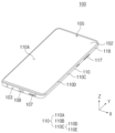
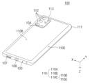
도 1 및 도 2를 참조하면, 일 실시 예에 따른 전자 장치(100)는, 제1 면(또는 전면)(110A), 제2 면(또는 후면)(110B), 및 제1 면(110A) 및 제2 면(110B) 사이의 공간을 둘러싸는 측면(110C)을 포함하는 하우징(110)을 포함할 수 있다. Referring to FIGS. 1 and 2, an electronic device (100) according to one embodiment may include a housing (110) including a first side (or front side) (110A), a second side (or back side) (110B), and a side surface (110C) surrounding a space between the first side (110A) and the second side (110B).
다른 실시 예(미도시)에서, 하우징(110)은, 도 1의 제1 면(110A), 제2 면(110B) 및 측면(110C)들 중 일부를 형성하는 구조를 지칭할 수도 있다. In another embodiment (not shown), the housing (110) may refer to a structure forming part of the first side (110A), the second side (110B), and the side surface (110C) of FIG. 1.
일 실시 예에 따르면, 제1 면(110A)은 적어도 일부분이 실질적으로 투명한 전면 플레이트(102)(예: 다양한 코팅 레이어들을 포함하는 글라스 플레이트, 또는 폴리머 플레이트)에 의하여 형성될 수 있다. 제2 면(110B)은 실질적으로 불투명한 후면 플레이트(111)에 의하여 형성될 수 있다. 상기 후면 플레이트(111)는, 예를 들어, 코팅 또는 착색된 유리, 세라믹, 폴리머, 금속(예: 알루미늄, 스테인레스 스틸(STS), 또는 마그네슘), 또는 상기 물질들 중 적어도 둘의 조합에 의하여 형성될 수 있다. 상기 측면(110C)은, 전면 플레이트(102) 및 후면 플레이트(111)와 결합하며, 금속 및/또는 폴리머를 포함하는 측면 베젤 구조(또는 “프레임 구조”)(118)에 의하여 형성될 수 있다. According to one embodiment, the first side (110A) can be formed by a front plate (102) that is at least partially substantially transparent (e.g., a glass plate including various coating layers, or a polymer plate). The second side (110B) can be formed by a substantially opaque back plate (111). The back plate (111) can be formed by, for example, coated or colored glass, ceramic, polymer, metal (e.g., aluminum, stainless steel (STS), or magnesium), or a combination of at least two of the foregoing materials. The side surface (110C) can be formed by a side bezel structure (or “frame structure”) (118) that is joined to the front plate (102) and the back plate (111) and includes a metal and/or a polymer.
어떤 실시 예에서, 후면 플레이트(111) 및 측면 베젤 구조(118)는 일체로 형성되고 동일한 물질(예: 알루미늄과 같은 금속 물질)을 포함할 수 있다.In some embodiments, the back plate (111) and the side bezel structure (118) may be formed integrally and include the same material (e.g., a metal material such as aluminum).
도시된 실시 예에서, 상기 전면 플레이트(102)는, 상기 제1 면(110A)으로부터 상기 후면 플레이트(111) 쪽으로 휘어져 심리스하게(seamless) 연장된 2개의 제1 영역(110D)들을, 상기 전면 플레이트(102)의 긴 엣지(long edge) 양단에 포함할 수 있다. In the illustrated embodiment, the front plate (102) may include two first regions (110D) extending seamlessly from the first side (110A) toward the rear plate (111) at both ends of a long edge of the front plate (102).
도시된 실시 예(도 2 참조)에서, 상기 후면 플레이트(111)는, 상기 제2 면(110B)으로부터 상기 전면 플레이트(102) 쪽으로 휘어져 심리스하게 연장된 2개의 제2 영역(110E)들을, 상기 후면 플레이트(111)의 긴 엣지 양단에 포함할 수 있다. In the illustrated embodiment (see FIG. 2), the rear plate (111) may include two second regions (110E) that extend seamlessly from the second surface (110B) toward the front plate (102), at both ends of the long edge of the rear plate (111).
어떤 실시 예에서, 상기 전면 플레이트(102)(또는 상기 후면 플레이트(111))는 상기 제1 영역(110D)들(또는 상기 제2 영역(110E)들) 중 하나 만을 포함할 수 있다. 다른 실시 예에서, 상기 전면 플레이트(102)(또는 상기 후면 플레이트(111))는 상기 제1 영역(110D)들 (또는 제2 영역(110E)들) 중 일부를 포함하지 않을 수 있다. In some embodiments, the front plate (102) (or the back plate (111)) may include only one of the first regions (110D) (or the second regions (110E)). In other embodiments, the front plate (102) (or the back plate (111)) may not include some of the first regions (110D) (or the second regions (110E)).
상기 실시 예들에서, 상기 전자 장치(100)의 측면에서 볼 때, 측면 베젤 구조(118)는, 상기와 같은 제1 영역(110D)들 또는 제2 영역(110E)들이 포함되지 않는 측면 쪽(예: 단변)에서는 제1 두께(또는 폭)을 가지고, 상기 제1 영역(110D)들 또는 제2 영역(110E)들을 포함한 측면 쪽(예: 장변)에서는 상기 제1 두께보다 얇은 제2 두께를 가질 수 있다.In the above embodiments, when viewed from the side of the electronic device (100), the side bezel structure (118) may have a first thickness (or width) on a side (e.g., a short side) that does not include the first regions (110D) or the second regions (110E) as described above, and may have a second thickness that is thinner than the first thickness on a side (e.g., a long side) that includes the first regions (110D) or the second regions (110E).
일 실시 예에 따르면, 전자 장치(100)는 디스플레이(101), 오디오 모듈(103, 104, 107), 센서 모듈(미도시, 예를 들어 디스플레이(101) 아래에 배치되거나, 디스플레이(101)에 실장될 수 있음(Under Display)), 카메라 모듈(105, 112), 키 입력 장치(117), 발광 소자(미도시, 예를 들어 디스플레이(101) 아래에 배치되거나, 디스플레이(101)에 실장될 수 있음(Under Display)), 및 커넥터 홀(108) 중 적어도 하나 이상을 포함할 수 있다. 어떤 실시 예에서, 전자 장치(100)는, 구성요소들 중 적어도 하나(예: 키 입력 장치(117), 또는 발광 소자)를 생략하거나 다른 구성요소를 추가적으로 포함할 수 있다.According to one embodiment, the electronic device (100) may include at least one of a display (101), an audio module (103, 104, 107), a sensor module (not shown, for example, positioned under the display (101) or mounted on the display (101) (Under Display)), a camera module (105, 112), a key input device (117), a light-emitting element (not shown, for example, positioned under the display (101) or mounted on the display (101) (Under Display)), and a connector hole (108). In some embodiments, the electronic device (100) may omit at least one of the components (e.g., the key input device (117) or the light-emitting element) or may additionally include other components.
디스플레이(101)는, 예를 들어, 전면 플레이트(102)의 상당 부분을 통하여 노출될 수 있다. 어떤 실시 예에서는, 상기 제1 면(110A), 및 상기 측면(110C)의 제1 영역(110D)들을 포함하는 전면 플레이트(102)를 통하여 상기 디스플레이(101)의 적어도 일부가 노출될 수 있다. The display (101) may be exposed, for example, through a significant portion of the front plate (102). In some embodiments, at least a portion of the display (101) may be exposed through the front plate (102), including the first surface (110A) and the first areas (110D) of the side surfaces (110C).
어떤 실시 예에서, 디스플레이(101)의 모서리는 상기 전면 플레이트(102)의 인접한 외곽 형상과 대체로 동일하게 형성될 수 있다. 다른 실시 예(미도시)에서, 디스플레이(101)가 노출되는 면적을 확장하기 위하여, 디스플레이(101)의 외곽과 전면 플레이트(102)의 외곽간의 간격은 대체로 동일하게 형성될 수 있다.In some embodiments, the corners of the display (101) may be formed to be substantially identical to the adjacent outer shape of the front plate (102). In other embodiments (not shown), in order to expand the area exposed to the display (101), the gap between the outer edge of the display (101) and the outer edge of the front plate (102) may be formed to be substantially identical.
일 실시 예에서, 하우징(110)의 표면(또는 전면 플레이트(102))은 디스플레이(101)가 시각적으로 노출됨에 따라 형성되는 화면 표시 영역을 포함할 수 있다. 일례로, 화면 표시 영역은 제1 면(110A), 및 측면의 제1 영역(110D)들을 포함할 수 있다. In one embodiment, the surface (or front plate (102)) of the housing (110) may include a screen display area formed as the display (101) is visually exposed. As an example, the screen display area may include a first surface (110A) and first areas (110D) of the side surfaces.
일 실시 예에서, 화면 표시 영역(110A, 110D)은 사용자의 생체 정보를 획득하도록 구성된 센싱 영역(미도시)을 포함할 수 있다. 여기서, “화면 표시 영역(110A, 110D)이 센싱 영역을 포함함”의 의미는 센싱 영역의 적어도 일부가 화면 표시 영역(110A, 110D)에 겹쳐질(overlapped) 수 있는 것으로 이해될 수 있다. 예를 들어, 센싱 영역은 화면 표시 영역(110A, 110D)의 다른 영역과 마찬가지로 디스플레이(101)에 의해 시각 정보를 표시할 수 있고, 및 추가적으로 사용자의 생체 정보(예: 지문)를 획득할 수 있는 영역을 의미할 수 있다. In one embodiment, the screen display area (110A, 110D) may include a sensing area (not shown) configured to acquire biometric information of the user. Here, the meaning of “the screen display area (110A, 110D) includes the sensing area” may be understood to mean that at least a portion of the sensing area may overlap the screen display area (110A, 110D). For example, the sensing area may mean an area that can display visual information by the display (101) like other areas of the screen display area (110A, 110D) and additionally acquire biometric information of the user (e.g., a fingerprint).
일 실시 예에서, 디스플레이(101)의 화면 표시 영역(110A, 110D)은 제1 카메라 모듈(105)(예: 펀치 홀 카메라)이 시각적으로 노출될 있는 영역을 포함할 수 있다. 예를 들어, 상기 제1 카메라 모듈(105)이 노출된 영역은 가장자리의 적어도 일부가 화면 표시 영역(110A, 110D)에 의해 둘러싸일 수 있다. 다양한 실시 예에서, 상기 제1 카메라 모듈(105)은 복수의 카메라 모듈들을 포함할 수 있다. In one embodiment, the screen display area (110A, 110D) of the display (101) may include an area in which the first camera module (105) (e.g., a punch hole camera) is visually exposed. For example, the area in which the first camera module (105) is exposed may have at least a portion of an edge surrounded by the screen display area (110A, 110D). In various embodiments, the first camera module (105) may include a plurality of camera modules.
다른 실시 예(미도시)에서, 디스플레이(101)의 화면 표시 영역(110A, 110D)의 일부에는 리세스 또는 개구부(opening)가 형성되고, 상기 리세스 또는 상기 개구부(opening)와 정렬되는 오디오 모듈(미도시), 제1 센서 모듈(미도시), 및 발광 소자(미도시) 중 적어도 하나 이상을 포함할 수 있다. 다양한 실시 예에서, 상기 리세스는 노치(Notch)와 동일하거나 노치(Notch)에 상응할 수 있다.In another embodiment (not shown), a part of a screen display area (110A, 110D) of the display (101) may have a recess or opening formed therein, and may include at least one of an audio module (not shown), a first sensor module (not shown), and a light-emitting element (not shown) aligned with the recess or the opening. In various embodiments, the recess may be identical to or correspond to the notch.
다른 실시 예(미도시)에서, 디스플레이(101)는 화면 표시 영역(110A, 110D)의 배면에, 오디오 모듈, 센서 모듈 및 발광 소자 중 적어도 하나 이상을 포함할 수 있다. In another embodiment (not shown), the display (101) may include at least one of an audio module, a sensor module, and a light-emitting element on the back surface of the screen display area (110A, 110D).
다른 실시 예(미도시)에서, 디스플레이(101)는, 터치 감지 회로, 터치의 세기(압력)를 측정할 수 있는 압력 센서, 및/또는 자기장 방식의 스타일러스 펜을 검출하는 디지타이저와 결합되거나 인접하여 배치될 수 있다. In another embodiment (not shown), the display (101) may be coupled with or disposed adjacent to a touch sensing circuit, a pressure sensor capable of measuring the intensity (pressure) of a touch, and/or a digitizer that detects a magnetic field-type stylus pen.
어떤 실시 예에서, 상기 센서 모듈의 적어도 일부, 및/또는 키 입력 장치(117)의 적어도 일부는, 상기 측면(110C)(예: 제1 영역(110D)들 및/또는 상기 제2 영역(110E)들)에 배치될 수 있다. In some embodiments, at least a portion of the sensor module, and/or at least a portion of the key input device (117), may be positioned on the side (110C) (e.g., the first regions (110D) and/or the second regions (110E)).
오디오 모듈(103, 104, 107)은, 마이크 홀(103, 104) 및 스피커 홀(107)을 포함할 수 있다. 마이크 홀(103, 104)은 외부의 소리를 획득하기 위한 마이크가 내부에 배치될 수 있고, 어떤 실시 예에서는 소리의 방향을 감지할 수 있도록 복수개의 마이크가 배치될 수 있다. 스피커 홀(107)은, 외부 스피커 홀(107) 및 통화용 리시버 홀(미도시)을 포함할 수 있다. 어떤 실시 예에서는 스피커 홀(107)과 마이크 홀(103, 104)이 하나의 홀로 구현 될 수 있다. 다른 실시 예에서 마이크 홀(104)는 디스플레이(101) 아래에 배치되거나, 디스플레이(101)에 실장될 수 있다(Under Display).The audio module (103, 104, 107) may include a microphone hole (103, 104) and a speaker hole (107). The microphone hole (103, 104) may have a microphone placed inside to acquire external sound, and in some embodiments, multiple microphones may be placed to detect the direction of the sound. The speaker hole (107) may include an external speaker hole (107) and a receiver hole for calls (not shown). In some embodiments, the speaker hole (107) and the microphone hole (103, 104) may be implemented as a single hole. In other embodiments, the microphone hole (104) may be placed under the display (101) or mounted on the display (101) (Under Display).
일 실시 예에서, 전자 장치(100)는 스피커 홀(107)과 연통되는 스피커를 포함할 수 있다. 어떤 실시 예에서, 스피커는 스피커 홀(107)이 생략된 피에조 스피커를 포함할 수 있다. In one embodiment, the electronic device (100) may include a speaker in communication with the speaker hole (107). In some embodiments, the speaker may include a piezo speaker in which the speaker hole (107) is omitted.
센서 모듈(미도시)은, 전자 장치(100)의 내부의 작동 상태, 또는 외부의 환경 상태에 대응하는 전기 신호 또는 데이터 값을 생성할 수 있다. 예를 들어, 센서 모듈은, 하우징(110)의 제1 면(110A)에 배치된 제1 센서 모듈(예: 근접 센서), 하우징(110)의 제2 면(110B)에 배치된 제2 센서 모듈(예: TOF 카메라), 상기 하우징(110)의 제2 면(110B)에 배치된 제3 센서 모듈(예: HRM 센서) 및/또는 디스플레이(101)에 결합되는 제4 센서 모듈(138)(예: 지문 센서)을 포함할 수 있다. A sensor module (not shown) can generate an electric signal or data value corresponding to an internal operating state of the electronic device (100) or an external environmental state. For example, the sensor module can include a first sensor module (e.g., a proximity sensor) disposed on a first surface (110A) of the housing (110), a second sensor module (e.g., a TOF camera) disposed on a second surface (110B) of the housing (110), a third sensor module (e.g., an HRM sensor) disposed on the second surface (110B) of the housing (110), and/or a fourth sensor module (138) (e.g., a fingerprint sensor) coupled to the display (101).
다양한 실시 예에서, 제2 센서 모듈(미도시)은 거리 측정을 위한 TOF 카메라를 포함할 수 있다. In various embodiments, the second sensor module (not shown) may include a TOF camera for distance measurement.
다양한 실시 예에서, 제4 센서 모듈(138)은 적어도 일부가 화면 표시 영역(110A, 110D) 아래에 배치될 수 있다. 일례로, 제4 센서 모듈은 디스플레이(101)의 배면에 형성된 리세스(139)에 배치될 수 있다. 예컨대, 제4 센서 모듈(138)은 화면 표시 영역(110A, 110D)으로 노출되지 않으며, 화면 표시 영역(110A, 110D)의 적어도 일부에 센싱 영역을 형성할 수 있다. 어떤 실시 예에서(미도시), 상기 지문 센서는 하우징(110)의 제1 면(110A)(예: 화면 표시 영역(110A, 110D))뿐만 아니라 제2 면(110B)에 배치될 수 있다. In various embodiments, the fourth sensor module (138) may be disposed at least partially below the display area (110A, 110D). For example, the fourth sensor module may be disposed in a recess (139) formed on the back surface of the display (101). For example, the fourth sensor module (138) may not be exposed to the display area (110A, 110D) and may form a sensing area in at least a portion of the display area (110A, 110D). In some embodiments (not shown), the fingerprint sensor may be disposed on the second surface (110B) as well as the first surface (110A) of the housing (110) (e.g., the display area (110A, 110D)).
다양한 실시 예에서, 전자 장치(100)는, 도시되지 않은 센서 모듈, 예를 들어, 제스처 센서, 자이로 센서, 기압 센서, 마그네틱 센서, 가속도 센서, 그립 센서, 컬러 센서, IR(infrared) 센서, 생체 센서, 온도 센서, 습도 센서, 또는 조도 센서 중 적어도 하나를 더 포함할 수 있다.In various embodiments, the electronic device (100) may further include at least one of a sensor module not shown, for example, a gesture sensor, a gyro sensor, a barometric pressure sensor, a magnetic sensor, an acceleration sensor, a grip sensor, a color sensor, an infrared (IR) sensor, a biometric sensor, a temperature sensor, a humidity sensor, or an illuminance sensor.
카메라 모듈(105, 112)은, 전자 장치(100)의 제1 면(110A)으로 노출되는 제1 카메라 모듈(105)(예: 펀치 홀 카메라), 및 제2 면(110B)으로 노출되는 제2 카메라 모듈(112), 및/또는 플래시(113)를 포함할 수 있다. The camera module (105, 112) may include a first camera module (105) (e.g., a punch hole camera) exposed to the first side (110A) of the electronic device (100), a second camera module (112) exposed to the second side (110B), and/or a flash (113).
일 실시 예에서, 제1 카메라 모듈(105)는 제1 면(110A) 중 화면 표시 영역(110D)의 일부를 통해 노출될 수 있다. 일례로, 제1 카메라 모듈(105)는 디스플레이(101)의 일부에 형성된 개구(미도시)를 통해 화면 표시 영역(110D)의 일부 영역으로 노출될 수 있다. In one embodiment, the first camera module (105) may be exposed through a portion of the screen display area (110D) of the first surface (110A). For example, the first camera module (105) may be exposed through a portion of the screen display area (110D) through an opening (not shown) formed in a portion of the display (101).
일 실시 예에서, 제2 카메라 모듈(112)는 복수의 카메라 모듈들(예: 듀얼 카메라, 또는 트리플 카메라)를 포함할 수 있다. 다만, 제2 카메라 모듈(112)이 반드시 복수의 카메라 모듈들을 포함하는 것으로 한정되는 것은 아니며 하나의 카메라 모듈을 포함할 수도 있다. In one embodiment, the second camera module (112) may include multiple camera modules (e.g., dual cameras or triple cameras). However, the second camera module (112) is not necessarily limited to including multiple camera modules and may include one camera module.
상기 카메라 모듈들(105, 112)은, 하나 또는 복수의 렌즈들, 이미지 센서, 및/또는 이미지 시그널 프로세서를 포함할 수 있다. 플래시(113)는, 예를 들어, 발광 다이오드 또는 제논 램프(xenon lamp)를 포함할 수 있다. 어떤 실시 예에서는, 2개 이상의 렌즈들(적외선 카메라, 광각 및 망원 렌즈) 및 이미지 센서들이 전자 장치(100)의 한 면에 배치될 수 있다.The camera modules (105, 112) may include one or more lenses, an image sensor, and/or an image signal processor. The flash (113) may include, for example, a light emitting diode or a xenon lamp. In some embodiments, two or more lenses (infrared camera, wide-angle and telephoto lenses) and image sensors may be arranged on one side of the electronic device (100).
키 입력 장치(117)는, 하우징(110)의 측면(110C)에 배치될 수 있다. 다른 실시 예에서는, 전자 장치(100)는 상기 언급된 키 입력 장치(117) 중 일부 또는 전부를 포함하지 않을 수 있고 포함되지 않은 키 입력 장치(117)는 디스플레이(101) 상에 소프트 키와 같은 다른 형태로 구현될 수 있다. 어떤 실시 예에서, 키 입력 장치는 화면 표시 영역(110A, 110D)에 포함된 센싱 영역을 형성하는 센서 모듈(예: 제4 센서 모듈(138))을 포함할 수 있다.The key input device (117) may be arranged on a side (110C) of the housing (110). In other embodiments, the electronic device (100) may not include some or all of the above-mentioned key input devices (117), and the key input devices (117) that are not included may be implemented in other forms, such as soft keys, on the display (101). In some embodiments, the key input device may include a sensor module (e.g., a fourth sensor module (138)) forming a sensing area included in the screen display area (110A, 110D).
발광 소자는, 예를 들어, 하우징(110)의 제1 면(110A)에 배치될 수 있다. 발광 소자는, 예를 들어, 전자 장치(100)의 상태 정보를 광 형태로 제공할 수 있다. 다른 실시 예에서, 발광 소자는, 예를 들어, 제1 카메라 모듈(105)의 동작과 연동되는 광원을 제공할 수 있다. 발광 소자는, 예를 들어, LED, IR LED 및/또는 제논 램프를 포함할 수 있다.The light-emitting element may be disposed, for example, on the first surface (110A) of the housing (110). The light-emitting element may provide, for example, status information of the electronic device (100) in the form of light. In another embodiment, the light-emitting element may provide a light source that is linked to the operation of, for example, the first camera module (105). The light-emitting element may include, for example, an LED, an IR LED, and/or a xenon lamp.
커넥터 홀(108)은, 외부 전자 장치와 전력 및/또는 데이터를 송수신하기 위한 커넥터(예를 들어, USB 커넥터)를 수용할 수 있는 제1 커넥터 홀(108), 및/또는 외부 전자 장치와 오디오 신호를 송수신하기 위한 커넥터를 수용할 수 있는 제2 커넥터 홀(미도시)(예를 들어, 이어폰 잭)을 포함할 수 있다.The connector hole (108) may include a first connector hole (108) that can accommodate a connector (e.g., a USB connector) for transmitting and receiving power and/or data with an external electronic device, and/or a second connector hole (not shown) that can accommodate a connector (e.g., an earphone jack) for transmitting and receiving audio signals with an external electronic device.
도 3는 일 실시 예에 따른 전자 장치의 분해 사시도이다. FIG. 3 is an exploded perspective view of an electronic device according to one embodiment.
도 3를 참조하면, 전자 장치(100)는, 전면 플레이트(120)(예: 도 1의 전면(110A) 및 제1 영역(110D)), 디스플레이(130)(예: 도 1의 디스플레이(101)), 브라켓(140)(예: 도 1의 측면의 일부(110C)), 제1 지지 구조(142)(예: 플레이트 구조), 제1 인쇄 회로 기판(151), 제2 인쇄 회로 기판(152)(예: PCB), 배터리(159), 리어 케이스(160), 안테나(170), 및 후면 플레이트(180)(예: 도 1의 후면(110B) 및 제2 영역(110E))를 포함할 수 있다. Referring to FIG. 3, the electronic device (100) may include a front plate (120) (e.g., the front (110A) and the first region (110D) of FIG. 1), a display (130) (e.g., the display (101) of FIG. 1), a bracket (140) (e.g., a portion of the side (110C) of FIG. 1), a first support structure (142) (e.g., a plate structure), a first printed circuit board (151), a second printed circuit board (152) (e.g., a PCB), a battery (159), a rear case (160), an antenna (170), and a rear plate (180) (e.g., the rear (110B) and the second region (110E) of FIG. 1).
어떤 실시 예에서, 전자 장치(100)는, 구성요소들 중 적어도 하나(예: 제1 지지 구조(142), 또는 리어 케이스(160))를 생략하거나 다른 구성요소를 추가적으로 포함할 수 있다. 전자 장치(100)의 구성요소들 중 적어도 하나는, 도 1, 또는 도 2의 전자 장치(100)의 구성요소들 중 적어도 하나와 동일, 또는 유사할 수 있으며, 중복되는 설명은 이하 생략한다.In some embodiments, the electronic device (100) may omit at least one of the components (e.g., the first support structure (142) or the rear case (160)) or may additionally include other components. At least one of the components of the electronic device (100) may be identical to or similar to at least one of the components of the electronic device (100) of FIG. 1 or FIG. 2, and any redundant description will be omitted below.
일 실시 예에서, 브라켓(140)은 전자 장치(100)의 표면(예: 도 1의 측면(110C)의 일부)을 형성하는 프레임 구조(141), 및 프레임 구조(141)로부터 전자 장치(100)의 내측으로 연장되는 제1 지지 구조(142)를 포함할 수 있다. In one embodiment, the bracket (140) may include a frame structure (141) forming a surface of the electronic device (100) (e.g., a portion of the side surface (110C) of FIG. 1), and a first support structure (142) extending inwardly of the electronic device (100) from the frame structure (141).
제1 지지 구조(142)는, 전자 장치(100) 내부에 위치되고, 프레임 구조(141)와 연결되거나, 또는 프레임 구조(141)와 일체로 형성될 수 있다. 제1 지지 구조(142)는, 예를 들어, 금속 재질 및/또는 비금속 (예: 폴리머) 재질로 형성될 수 있다. 어떤 실시 예에서, 제1 지지 구조(142)는, 전자 장치(100) 내부에 배치되어 브라켓(140)와 연결될 수 있거나, 브라켓(140)와 일체로 형성될 수 있다. 제1 지지 구조(142)는, 일면에 디스플레이(130)가 결합되고 타면에 제1 인쇄 회로 기판(151) 또는 제2 인쇄 회로 기판(152) 중 적어도 하나가 결합될 수 있다. 제1 인쇄 회로 기판(151) 또는 제2 인쇄 회로 기판(152) 중 적어도 하나에는, 프로세서, 메모리, 및/또는 인터페이스가 장착될 수 있다. 프로세서는, 예를 들어, 중앙처리장치, 어플리케이션 프로세서, 그래픽 처리 장치, 이미지 시그널 프로세서, 센서 허브 프로세서, 또는 커뮤니케이션 프로세서 중 하나 또는 그 이상을 포함할 수 있다.The first support structure (142) may be positioned inside the electronic device (100) and connected to the frame structure (141) or formed integrally with the frame structure (141). The first support structure (142) may be formed of, for example, a metal material and/or a non-metallic (e.g., polymer) material. In some embodiments, the first support structure (142) may be positioned inside the electronic device (100) and connected to the bracket (140) or formed integrally with the bracket (140). The first support structure (142) may have a display (130) coupled to one surface and at least one of a first printed circuit board (151) or a second printed circuit board (152) coupled to the other surface. At least one of the first printed circuit board (151) or the second printed circuit board (152) may be equipped with a processor, a memory, and/or an interface. The processor may include, for example, one or more of a central processing unit, an application processor, a graphics processing unit, an image signal processor, a sensor hub processor, or a communications processor.
메모리는, 예를 들어, 휘발성 메모리 또는 비휘발성 메모리를 포함할 수 있다. The memory may include, for example, volatile memory or non-volatile memory.
인터페이스는, 예를 들어, HDMI(high definition multimedia interface), USB(universal serial bus) 인터페이스, SD카드 인터페이스, 및/또는 오디오 인터페이스를 포함할 수 있다. 인터페이스는, 예를 들어, 전자 장치(100)를 외부 전자 장치와 전기적 또는 물리적으로 연결시킬 수 있으며, USB 커넥터, SD 카드/MMC 커넥터, 또는 오디오 커넥터를 포함할 수 있다.The interface may include, for example, a high definition multimedia interface (HDMI), a universal serial bus (USB) interface, an SD card interface, and/or an audio interface. The interface may electrically or physically connect the electronic device (100) to an external electronic device, for example, and may include a USB connector, an SD card/MMC connector, or an audio connector.
배터리(159)는 전자 장치(100)의 적어도 하나의 구성 요소에 전력을 공급하기 위한 장치로서, 예를 들면, 재충전 불가능한 1차 전지, 또는 재충전 가능한 2차 전지, 또는 연료 전지를 포함할 수 있다. 배터리(159)의 적어도 일부는, 예를 들어, 제1 인쇄 회로 기판(151) 또는 제2 인쇄 회로 기판(152) 중 적어도 하나와 실질적으로 동일 평면 상에 배치될 수 있다. 배터리(159)는 전자 장치(100) 내부에 일체로 배치될 수 있고, 전자 장치(100)와 탈부착 가능하게 배치될 수도 있다.The battery (159) is a device for supplying power to at least one component of the electronic device (100), and may include, for example, a non-rechargeable primary battery, a rechargeable secondary battery, or a fuel cell. At least a portion of the battery (159) may be arranged substantially on the same plane as, for example, at least one of the first printed circuit board (151) or the second printed circuit board (152). The battery (159) may be arranged integrally within the electronic device (100), or may be arranged to be detachably attached to the electronic device (100).
안테나(170)는, 후면 플레이트(180)와 배터리(159) 사이에 배치될 수 있다. 안테나(170)는, 예를 들어, NFC(near field communication) 안테나, 무선 충전 안테나, 및/또는 MST(magnetic secure transmission) 안테나를 포함할 수 있다. 안테나(170)는, 예를 들어, 외부 장치와 근거리 통신을 하거나, 충전에 필요한 전력을 무선으로 송수신 할 수 있다. 다른 실시 예에서는, 브라켓(140) 및/또는 상기 제1 지지 구조(142)의 일부 또는 그 조합에 의하여 안테나 구조가 형성될 수 있다.Antenna (170) may be positioned between the back plate (180) and the battery (159). The antenna (170) may include, for example, a near field communication (NFC) antenna, a wireless charging antenna, and/or a magnetic secure transmission (MST) antenna. The antenna (170) may, for example, perform short-range communication with an external device or wirelessly transmit and receive power required for charging. In another embodiment, the antenna structure may be formed by a portion or a combination of the bracket (140) and/or the first support structure (142).
다양한 실시 예에서, 카메라 모듈(105)은 렌즈가 전자 장치(100)의 전면(110A)으로 노출되도록 하우징(110) 내부에 배치될 수 있다. 예를 들어, 카메라 모듈(105)은 디스플레이(130)의 배면에 형성된 홀 또는 리세스(137)의 내부에 배치되는 펀치 홀 카메라를 포함할 수 있다. In various embodiments, the camera module (105) may be positioned inside the housing (110) such that the lens is exposed to the front (110A) of the electronic device (100). For example, the camera module (105) may include a punch hole camera positioned inside a hole or recess (137) formed on the back surface of the display (130).
다양한 실시 예에서, 카메라 모듈(112)은 렌즈가 전자 장치(100)의 후면(110B)의 카메라 영역(110H)으로 노출되도록 하우징(110) 내부에 배치될 수 있다. 예를 들어, 카메라 모듈(112)은 제1 인쇄 회로 기판(151)에 배치될 수 있다. In various embodiments, the camera module (112) may be positioned inside the housing (110) such that the lens is exposed to the camera area (110H) of the rear (110B) of the electronic device (100). For example, the camera module (112) may be positioned on the first printed circuit board (151).
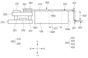
일 실시 예에서, 제1 인쇄 회로 기판(151)과 제2 인쇄 회로 기판(152)은 연성 회로 기판(190)을 통해 서로 연결될 수 있다. 도 3을 참조하면, 제1 인쇄 회로 기판(151)과 제2 인쇄 회로 기판(152)은 서로 이격되게 배치될 수 있다. 제1 인쇄 회로 기판(151)과 제2 인쇄 회로 기판(152) 사이에는 배터리(159)가 배치될 수 있다. In one embodiment, the first printed circuit board (151) and the second printed circuit board (152) may be connected to each other through a flexible circuit board (190). Referring to FIG. 3, the first printed circuit board (151) and the second printed circuit board (152) may be spaced apart from each other. A battery (159) may be placed between the first printed circuit board (151) and the second printed circuit board (152).
일 실시 예에서, 연성 회로 기판(190)은 제1 인쇄 회로 기판(151), 제2 인쇄 회로 기판(152) 및 외부 인터페이스 부재(미도시, 예: USB 리셉터클)를 전기적으로 연결할 수 있다. 예를 들어, 연성 회로 기판(190)의 제1 단부는 제1 인쇄 회로 기판(151)과 연결될 수 있고, 제2 단부는 제2 인쇄 회로 기판(152)과 연결될 수 있고, 제3 단부는 외부 인터페이스 부재와 연결될 수 있다. 예를 들어, 연성 회로 기판(190)은 제1 인쇄 회로 기판(151) 및 제2 인쇄 회로 기판(152)과 외부 인터페이스 부재를 통하여 연결되는 다른 전자 장치(미도시)를 연결할 수 있다. 제1 인쇄 회로 기판(151) 및 제2 인쇄 회로 기판(152)은 외부 인터페이스 부재를 통하여 연결되는 다른 전자 장치(미도시)와 전기적 및/또는 전자적 신호를 주고 받을 수 있다. In one embodiment, the flexible circuit board (190) can electrically connect a first printed circuit board (151), a second printed circuit board (152), and an external interface member (not shown, for example, a USB receptacle). For example, a first end of the flexible circuit board (190) can be connected to the first printed circuit board (151), a second end can be connected to the second printed circuit board (152), and a third end can be connected to the external interface member. For example, the flexible circuit board (190) can connect another electronic device (not shown) connected to the first printed circuit board (151) and the second printed circuit board (152) through the external interface member. The first printed circuit board (151) and the second printed circuit board (152) can exchange electrical and/or electronic signals with another electronic device (not shown) connected through the external interface member.
일 실시 예에서, 연성 회로 기판(190)은 배터리(159)를 가로질러 연장될 수 있다. 예를 들어, 이격 배치되는 둘 이상의 인쇄 회로 기판들(151, 152)은, 연성 회로 기판(190)을 통해서 전기적 및/또는 전자적 신호(또는 정보)를 주고 받을 수 있다. 일 실시 예에서, 연성 회로 기판(190)은 적어도 일부가 플렉서블하게 이루어질 수 있다. 예를 들어, 연성 회로 기판(190)은 적어도 일부가 플렉서블하게 구부러지는 벤딩 부분을 포함할 수 있다. 일 실시 예에 따른 벤딩 부분은, 연성 회로 기판(190)이 전자 장치(100) 내부에 배치되는 컴포넌트들의 사이(예: 배터리(159)와 제1 연성 회로 기판(151)의 사이 또는 배터리(159)와 제2 연성 회로 기판(152)의 사이)로 연장 되도록 구부러질 수 있다. In one embodiment, the flexible circuit board (190) can extend across the battery (159). For example, two or more spaced apart printed circuit boards (151, 152) can exchange electrical and/or electronic signals (or information) through the flexible circuit board (190). In one embodiment, the flexible circuit board (190) can be formed at least in part to be flexible. For example, the flexible circuit board (190) can include a bend portion that is at least in part flexibly bent. The bend portion according to one embodiment can be bent such that the flexible circuit board (190) extends between components disposed within the electronic device (100) (e.g., between the battery (159) and the first flexible circuit board (151) or between the battery (159) and the second flexible circuit board (152).
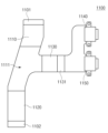
도 4는 일 실시 예에 따른 전자 장치의 연성 회로 기판을 도시하는 도면이다.FIG. 4 is a diagram illustrating a flexible circuit board of an electronic device according to one embodiment.
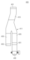
일 실시 예에서, 전자 장치(100)는 연성 회로 기판(400), 및 연성 회로 기판(400)에 연결되는 외부 인터페이스 부재(440)를 포함할 수 있다. In one embodiment, the electronic device (100) may include a flexible circuit board (400) and an external interface member (440) connected to the flexible circuit board (400).
도 4를 참조하면, 연성 회로 기판(400)은 메인 영역(410), 제1 분기(branch) 영역(420), 및 제2 분기(branch) 영역(430)을 포함할 수 있다. 일 실시 예에 따르면, 메인 영역(410)은 제1 커넥터(401)과 연결되는 도전성 패턴을 포함할 수 있다. 일 실시 예에 따르면, 제1 분기 영역(420)은 메인 영역(410)에 포함된 도전성 패턴의 일부를 포함할 수 있다. 제2 분기 영역(430)은 메인 영역(410)에 포함된 도전성 패턴 중 제1 분기 영역(420)에 포함되지 않은 적어도 일부를 포함할 수 있다. 도 4를 참조하면, 메인 영역(410)으로부터 제1 분기 영역(420)이 연장되는 방향(예: 도면을 기준으로 하부 방향)과 메인 영역(410)으로부터 제2 분기 영역(430)이 연장되는 방향(예: 도면을 기준으로 하부 방향)은 서로 동일할 수 있다. Referring to FIG. 4, the flexible circuit board (400) may include a main region (410), a first branch region (420), and a second branch region (430). According to one embodiment, the main region (410) may include a conductive pattern connected to the first connector (401). According to one embodiment, the first branch region (420) may include a portion of the conductive pattern included in the main region (410). The second branch region (430) may include at least a portion of the conductive pattern included in the main region (410) that is not included in the first branch region (420). Referring to FIG. 4, a direction in which the first branch region (420) extends from the main region (410) (e.g., downward with respect to the drawing) and a direction in which the second branch region (430) extends from the main region (410) (e.g., downward with respect to the drawing) may be the same as each other.
연성 회로 기판(400)은 적어도 일부가 벤딩 가능하도록 플렉서블하게 형성될 수 있다. 연성 회로 기판(400)은 전자 장치(100)의 내부에 포함된 컴포넌트들(예: 도 3의 제1 인쇄 회로 기판(151), 제2 인쇄 회로 기판(152))을 서로 전기적으로 연결하도록 구성될 수 있다. The flexible circuit board (400) may be formed to be flexible so that at least a portion thereof is bendable. The flexible circuit board (400) may be configured to electrically connect components included within the electronic device (100) to each other (e.g., the first printed circuit board (151) and the second printed circuit board (152) of FIG. 3).
일 실시 예에서, 메인 영역(410)은 제1 분기 영역(420)과 제2 분기 영역(430)으로 나뉘는 섹션인 슬릿(slit) 부분(411)을 포함할 수 있다. 일 실시 예에서, 메인 영역(410)은 제1 인쇄 회로 기판(예: 도 3의 제1 인쇄 회로 기판(151))과 전기적으로 연결될 수 있다. 예를 들어, 메인 영역(410)은 제2 분기 영역(430)과 함께 이격 배치된 제1 인쇄 회로 기판과 제2 인쇄 회로 기판(예: 도 3의 제2 인쇄 회로 기판(152))을 전기적으로 연결할 수 있다. 예를 들어, 메인 영역(410)은 제1 인쇄 회로 기판에 결합되는 제1 커넥터(401)를 포함할 수 있다. 예를 들어, 제1 커넥터(401)는 메인 영역(410)의 제1 단부에 배치될 수 있다. 어떤 실시 예에 따르면, 제1 커넥터(401)는 메인 영역(410)의 제1 단부와 접촉하는 컨택 커넥터(Contact Connector)를 포함할 수 있다.In one embodiment, the main region (410) may include a slit portion (411) that is a section divided into a first branch region (420) and a second branch region (430). In one embodiment, the main region (410) may be electrically connected to a first printed circuit board (e.g., the first printed circuit board (151) of FIG. 3). For example, the main region (410) may electrically connect a first printed circuit board and a second printed circuit board (e.g., the second printed circuit board (152) of FIG. 3) that are spaced apart from each other together with the second branch region (430). For example, the main region (410) may include a first connector (401) coupled to the first printed circuit board. For example, the first connector (401) may be disposed at a first end of the main region (410). According to some embodiments, the first connector (401) may include a contact connector that contacts the first end of the main region (410).
일 실시 예에서, 제1 분기 영역(420)은 외부 인터페이스 부재(440)와 전기적으로 연결될 수 있다. 제1 분기 영역(420)은 메인 영역(410)과 함께 제1 인쇄 회로 기판(예: 도 3의 제1 인쇄 회로 기판(151))에 포함된 제어 회로(미도시)와 외부 인터페이스 부재(440)를 전기적으로 연결할 수 있다. 예를 들어, 외부 인터페이스 부재(440)는 제1 분기 영역(420)의 제2 단부에 결합될 수 있다. 예를 들어, 외부 인터페이스 부재(440)는 USB 리셉터클(USB Type-B 또는 USB Type-C)을 포함할 수 있다. 다른 예를 들어, 외부 인터페이스 부재(440)는 USB 이어폰과 연결할 수 있는 리셉터클을 포함할 수 있다. 이 경우, 외부 인터페이스 부재(440)는 마이크 신호를 수신하거나, 오디오 신호를 외부로 출력할 수 있다. 다른 예를 들어, 외부 인터페이스 부재(440)는 HDMI 커넥터가 연결될 수 있도록 형성된 컴포넌트를 포함할 수 있다. 다른 예를 들어, 외부 인터페이스 부재(440)는 디스플레이 포트(Display Port)가 연결될 수 있도록 형성된 컴포넌트를 포함할 수 있다. 일 실시 예에 따른 외부 인터페이스 부재(440)는 상술한 예시에 제한되지 않고, 외부 전자 장치와 연결될 수 있도록 형성된 컴포넌트를 포함할 수 있다.In one embodiment, the first branch region (420) may be electrically connected to an external interface member (440). The first branch region (420) may electrically connect a control circuit (not shown) included in a first printed circuit board (e.g., the first printed circuit board (151) of FIG. 3) together with the main region (410) and the external interface member (440). For example, the external interface member (440) may be coupled to a second end of the first branch region (420). For example, the external interface member (440) may include a USB receptacle (USB Type-B or USB Type-C). As another example, the external interface member (440) may include a receptacle that can be connected to a USB earphone. In this case, the external interface member (440) may receive a microphone signal or output an audio signal to the outside. As another example, the external interface member (440) may include a component formed so that an HDMI connector can be connected. For another example, the external interface member (440) may include a component formed to be able to connect a display port. The external interface member (440) according to one embodiment is not limited to the above-described examples and may include a component formed to be able to connect to an external electronic device.
일 실시 예에서, 제1 분기 영역(420)은 벤딩 부분(421)을 포함할 수 있다. 일 실시 예에 따른 연성 회로 기판(400)은 적어도 하나의 레이어를 적층한 구조로 형성될 수 있다. 예를 들어, 메인 영역(410), 제1 분기 영역(420) 및 제2 분기 영역(430)은 싱글 사이드 레이어(Single Side Layer), 더블 사이드 레이어(Double Side Layer) 또는 멀티 레이어(Multi Layer) 중에서 적어도 하나의 구조로 형성될 수 있다. 일 실시 예에 따르면, 벤딩 부분(421)은 협소한 공간에서 효율적인 벤딩 특성을 위해서, 적층된 레이어들 중에서 적어도 하나가 삭제된 구조로 형성될 수 있다. 예를 들어, 메인 영역(410), 제1 분기 영역(420) 및 제2 분기 영역(430)이 멀티 레이어의 구조로 형성된 경우, 벤딩 부분(421)은 더블 사이드 레이어 또는 싱글 사이드 레이어 중에서 어느 하나의 구조로 형성될 수 있다. 일부 레이어가 삭제된 벤딩 부분(421)은 쉽게 구부러질 수 있으므로 벤딩 특성이 향상될 수 있다.In one embodiment, the first branch region (420) may include a bending portion (421). The flexible circuit board (400) according to one embodiment may be formed with a structure in which at least one layer is laminated. For example, the main region (410), the first branch region (420), and the second branch region (430) may be formed with at least one structure from among a single side layer, a double side layer, or a multi layer. According to one embodiment, the bending portion (421) may be formed with a structure in which at least one of the laminated layers is deleted for efficient bending characteristics in a narrow space. For example, when the main region (410), the first branch region (420), and the second branch region (430) are formed with a multi-layer structure, the bending portion (421) may be formed with either a double side layer or a single side layer structure. The bending portion (421) from which some layers have been deleted can be easily bent, so that the bending characteristics can be improved.
벤딩 부분(421)은 전자 장치(100)의 내부에 포함된 다른 구조물들(예: 배터리(159), 스피커 모듈(예: 도 5의 스피커 모듈(500)) 사이로 연장되도록 벤딩될 수 있다. 일 실시 예에 따른 벤딩 부분(421)을 포함하는 제1 분기 영역(420)은 일정한 크기의 단차(gap or differential)를 갖도록 연장될 수 있다. 예를 들어 벤딩 부분(421)은, 제1 분기 영역(420)이 메인 영역(410)으로부터 연장되는 방향에 대해서 수직하는 방향으로 벤딩될 수 있다. 일 실시 예에 따른 제1 분기 영역(420)을 측면에서 바라보면, 제1 분기 영역(420)은 벤딩 부분(421)을 포함하므로, 벤딩 부분(421)에 의해서 형성되는 일정한 크기의 단차를 적어도 일부 포함할 수 있다. The bending portion (421) may be bent to extend between other structures included in the electronic device (100) (e.g., a battery (159), a speaker module (e.g., a speaker module (500) of FIG. 5)). The first branch region (420) including the bending portion (421) according to one embodiment may be extended to have a gap or differential of a predetermined size. For example, the bending portion (421) may be bent in a direction perpendicular to the direction in which the first branch region (420) extends from the main region (410). When the first branch region (420) according to one embodiment is viewed from the side, since the first branch region (420) includes the bending portion (421), it may at least partially include a gap of a predetermined size formed by the bending portion (421).
일 실시 예에서, 제2 분기 영역(430)은 제2 인쇄 회로 기판(예: 도 3의 제2 인쇄 회로 기판(152))과 전기적으로 연결될 수 있다. 제2 분기 영역(430)은 메인 영역(410)과 함께 이격 배치된 제1 인쇄 회로 기판(예: 도 3의 제1 인쇄 회로 기판(151))과 제2 인쇄 회로 기판을 전기적으로 연결할 수 있다. 예를 들어, 제2 분기 영역(430)은 제2 인쇄 회로 기판에 결합되는 제2 커넥터(403)를 포함할 수 있다. 예를 들어, 제2 커넥터(403)는 제2 분기 영역(430)의 제3 단부에 배치될 수 있다. 어떤 실시 예에 따르면, 제2 커넥터(403)는 제2 분기 영역(430)의 제3 단부와 접촉하는 컨택 커넥터(Contact Connector)를 포함할 수 있다. In one embodiment, the second branch region (430) can be electrically connected to a second printed circuit board (e.g., the second printed circuit board (152) of FIG. 3). The second branch region (430) can electrically connect a first printed circuit board (e.g., the first printed circuit board (151) of FIG. 3) and the second printed circuit board, which are spaced apart from the main region (410). For example, the second branch region (430) can include a second connector (403) coupled to the second printed circuit board. For example, the second connector (403) can be disposed at a third end of the second branch region (430). According to some embodiments, the second connector (403) can include a contact connector that contacts the third end of the second branch region (430).
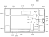
도 5는 일 실시 예에 따른, 연성 회로 기판을 포함하는 전자 장치의 내부 구조를 도시한 도면이다.FIG. 5 is a diagram illustrating the internal structure of an electronic device including a flexible circuit board according to one embodiment.
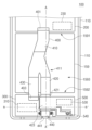
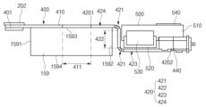
도 5를 참조하면, 전자 장치(100)는, 하우징(110) 및 하우징(110)의 내부에 배치되는 복수의 컴포넌트들을 포함할 수 있다. 예를 들어, 복수의 컴포넌트들은 메인 회로 기판(200)(예: 도 3의 제1 인쇄 회로 기판(151)), 서브 회로 기판(300)(예: 도 3의 제2 인쇄 회로 기판(152)), 배터리(159), 스피커 모듈(500), 연성 회로 기판(400)을 포함할 수 있다.Referring to FIG. 5, the electronic device (100) may include a housing (110) and a plurality of components arranged inside the housing (110). For example, the plurality of components may include a main circuit board (200) (e.g., the first printed circuit board (151) of FIG. 3), a sub-circuit board (300) (e.g., the second printed circuit board (152) of FIG. 3), a battery (159), a speaker module (500), and a flexible circuit board (400).
일 실시 예에 따르면, 메인 회로 기판(200)은 하우징(110)의 내부에 배치될 수 있다. 메인 회로 기판(200)은 제어 회로(230)를 포함할 수 있다. 예를 들어, 제어 회로(230)는 프로세서를 포함할 수 있다. 예를 들어, 제어 회로(230)는 통신 회로 또는 충전 회로 중에서 적어도 하나를 포함할 수 있다. 예를 들어, 제어 회로(230)는 통신 회로를 이용하여 유선 통신(예: USB를 이용한 데이터 통신)을 수행할 수 있다. 예를 들어, 제어 회로(230)는 통신 회로를 이용하여 무선 통신을 수행할 수 있다. 예를 들어, 제어 회로(230)는 충전 회로를 이용하여 배터리(159)에 전력을 충전할 수 있다. 다른 실시 예에 따르면, 제어 회로(230)는 서브 회로 기판(300)에 포함된 접속 회로(310)를 제어할 수 있다. According to one embodiment, the main circuit board (200) may be disposed inside the housing (110). The main circuit board (200) may include a control circuit (230). For example, the control circuit (230) may include a processor. For example, the control circuit (230) may include at least one of a communication circuit and a charging circuit. For example, the control circuit (230) may perform wired communication (e.g., data communication using USB) using the communication circuit. For example, the control circuit (230) may perform wireless communication using the communication circuit. For example, the control circuit (230) may charge power to the battery (159) using the charging circuit. According to another embodiment, the control circuit (230) may control a connection circuit (310) included in a sub-circuit board (300).
일 실시 예에 따르면, 메인 회로 기판(200)은 배터리(159)를 사이에 두고 서브 회로 기판(300)과 이격되어 배치될 수 있다. 메인 회로 기판(200)은 배터리(159)의 제1 측면(1591)과 마주보도록 배치될 수 있다. 일 실시 예에 따르면, 서브 회로 기판(300)은 하우징(110)의 내부에 배치될 수 있다. 일 실시 예에 따르면, 서브 회로 기판(300)은 배터리(159)의 제2 측면(1592)과 마주보도록 배치될 수 있다. 서브 회로 기판(300)은 접속 회로(310)를 포함할 수 있다. 일 실시 예에서, 접속 회로(310)는 전자 장치(100)에 대한 입출력 동작을 수행할 수 있다. 예를 들어, 접속 회로(310)는 전자 장치(100)의 입출력 장치를 전기적으로 연결할 수 있다. 예를 들어, 접속 회로(310)는 스피커 모듈(500)을 전기적으로 연결할 수 있고, 제어 회로(230)는 접속 회로(310)을 통하여 스피커 모듈(500)을 제어할 수 있다. 예를 들어, 접속 회로(310)는 사용자 입력에 대응한 햅틱 피드백을 제공하는 햅틱 모터(미도시)를 전기적으로 연결할 수 있고, 제어 회로 (230)는 접속 회로(310)을 통하여 햅틱 모터를 제어할 수 있다. 예를 들어, 접속 회로(310)는 외부(예: 사용자 또는 전자 입력 기기)로부터 타이핑 또는 터치를 입력 받는 키보드 리셉터클(미도시)을 전기적으로 연결할 수 있고, 제어 회로(230)는 접속 회로(310)을 통하여 키보드 리셉터클을 제어할 수 있다. 예를 들어, 접속 회로(310)는 무선 통신에 사용되는 적어도 하나의 안테나(예: 도 3의 안테나(170))를 전기적으로 연결할 수 있고, 제어 회로(230)은 접속 회로(310)를 통하여 적어도 하나의 안테나의 동작을 제어할 수 있다. 예를 들어, 적어도 하나의 안테나는 LDS 안테나(540) 또는 프레임 안테나(미도시) 중 적어도 하나를 포함할 수 있다. 도 5에는 전자 장치(100)가 LDS 안테나(540)를 포함하는 것으로 도시되었으나, 도시된 것에 한정되지 않고 다양한 형태의 무선 통신에 사용되는 안테나를 포함할 수 있다. According to one embodiment, the main circuit board (200) may be disposed spaced apart from the sub-circuit board (300) with the battery (159) therebetween. The main circuit board (200) may be disposed to face the first side (1591) of the battery (159). According to one embodiment, the sub-circuit board (300) may be disposed inside the housing (110). According to one embodiment, the sub-circuit board (300) may be disposed to face the second side (1592) of the battery (159). The sub-circuit board (300) may include a connection circuit (310). In one embodiment, the connection circuit (310) may perform input/output operations for the electronic device (100). For example, the connection circuit (310) may electrically connect an input/output device of the electronic device (100). For example, the connection circuit (310) can electrically connect the speaker module (500), and the control circuit (230) can control the speaker module (500) through the connection circuit (310). For example, the connection circuit (310) can electrically connect a haptic motor (not shown) that provides haptic feedback corresponding to a user input, and the control circuit (230) can control the haptic motor through the connection circuit (310). For example, the connection circuit (310) can electrically connect a keyboard receptacle (not shown) that receives typing or touch input from an external source (e.g., a user or an electronic input device), and the control circuit (230) can control the keyboard receptacle through the connection circuit (310). For example, the connection circuit (310) can electrically connect at least one antenna (e.g., antenna (170) of FIG. 3) used for wireless communication, and the control circuit (230) can control the operation of the at least one antenna through the connection circuit (310). For example, the at least one antenna can include at least one of an LDS antenna (540) or a frame antenna (not shown). Although the electronic device (100) is illustrated as including an LDS antenna (540) in FIG. 5, it is not limited to the illustrated one and can include various types of antennas used for wireless communication.
일 실시 예에 따르면, 연성 회로 기판(400)은 하우징(110)의 내부에 배치될 수 있다. 예를 들어, 연성 회로 기판(400)은 복수의 컴포넌트들과 전기적으로 연결될 수 있다. 예를 들어, 연성 회로 기판(400)은 메인 회로 기판(200), 서브 회로 기판(300) 및 외부 인터페이스 부재(440)의 사이에 전기적 및/또는 전자적 신호를 전달할 수 있다. According to one embodiment, the flexible circuit board (400) can be disposed inside the housing (110). For example, the flexible circuit board (400) can be electrically connected to a plurality of components. For example, the flexible circuit board (400) can transmit electrical and/or electronic signals between the main circuit board (200), the sub-circuit board (300), and the external interface member (440).
일 실시 예에 따르면, 연성 회로 기판(400)에는 제1 커넥터(401), 제2 커넥터(403) 및 외부 인터페이스 부재(440)가 연결될 수 있다. According to one embodiment, a first connector (401), a second connector (403), and an external interface member (440) may be connected to a flexible circuit board (400).
일 실시 예에 따르면, 제1 커넥터(401)는 메인 영역(410)의 제1 단부에 배치되어 메인 회로 기판(200)과 연성 회로 기판(400)을 전기적으로 및/또는 물리적으로 연결할 수 있다. 예를 들어, 제1 커넥터(401)는 보드-투-보드 커넥터(Board-To-Board Connector)를 포함할 수 있다. 다른 예에서 제1 커넥터(401)은 핀헤더 커넥터(Pin Header Connector)를 포함할 수 있다. 일 실시 예에 따르면, 제1 커넥터(401)는, 서브 회로 기판(300)으로부터 데이터를 송수신하고, 외부 인터페이스 부재(440)를 통해서 연결되는 외부 전자 장치(미도시)와 데이터를 교환하고, 전원 장치(미도시)로부터 전원을 공급 받을 수 있으므로, 제2 커넥터(402)에 포함된 핀(Pin)의 개수보다 많은 개수의 핀을 포함할 수 있다. 일 실시 예에 따르면, 메인 회로 기판(200)은 제1 커넥터(401)와 연결될 수 있도록 제1 커넥터(401)에 대응하는 소켓(Socket)용 커넥터를 더 포함할 수 있다.According to one embodiment, the first connector (401) may be arranged at a first end of the main region (410) to electrically and/or physically connect the main circuit board (200) and the flexible circuit board (400). For example, the first connector (401) may include a board-to-board connector. In another example, the first connector (401) may include a pin header connector. According to one embodiment, the first connector (401) may transmit and receive data from the sub-circuit board (300), exchange data with an external electronic device (not shown) connected through an external interface member (440), and receive power from a power supply device (not shown), and therefore, may include a greater number of pins than the number of pins included in the second connector (402). According to one embodiment, the main circuit board (200) may further include a connector for a socket corresponding to the first connector (401) so as to be connected to the first connector (401).
일 실시 예에 따르면, 제2 커넥터(403)는 제2 분기 영역(430)의 제2 단부에 배치되어 서브 회로 기판(300)과 연성 회로 기판(400)을 전기적으로 및/또는 물리적으로 연결할 수 있다. 예를 들어, 제2 커넥터(403)는 보드-투-보드 커넥터(Board-To-Board Connector)를 포함할 수 있다. 다른 예에서 제2 커넥터(403)은 핀헤더 커넥터(Pin Header Connector)를 포함할 수 있다. 일 실시 예에 따르면, 서브 회로 기판(300)은 제2 커넥터(403)와 연결될 수 있도록 제2 커넥터(403)에 대응하는 소켓(Socket)용 커넥터를 더 포함할 수 있다.According to one embodiment, the second connector (403) may be disposed at the second end of the second branch region (430) to electrically and/or physically connect the sub-circuit board (300) and the flexible circuit board (400). For example, the second connector (403) may include a board-to-board connector. In another example, the second connector (403) may include a pin header connector. According to one embodiment, the sub-circuit board (300) may further include a socket connector corresponding to the second connector (403) so as to be connected to the second connector (403).
일 실시 예에 따르면, 외부 인터페이스 부재(440)는 제1 분기 영역(420)의 제3 단부에 배치될 수 있다. 예를 들어, 외부 인터페이스 부재(440)는 하우징(110) 내부에 배치되는 브라켓과 스크류(screw) 결합할 수 있다. 또는, 외부 인터페이스 부재(440)는 하우징(110) 내부에 배치되는 브라켓 및 서브 회로 기판(300)의 일부와 스크류 결합할 수 있다. 외부 인터페이스 부재(440)가 브라켓과 적어도 일부 스크류 결합함에 따라서, 외부 인터페이스 부재(440)의 움직임이 최소화되도록 외부 인터페이스 부재(440)가 고정될 수 있다. 일 실시 예에 따르면, 외부 인터페이스 부재(440)를 통해서 USB 이어폰 전자 장치(100)에 연결될 수 있다. 이 경우, 외부 인터페이스 부재(440)는 USB 리셉터클을 포함할 수 있다.According to one embodiment, the external interface member (440) may be disposed at the third end of the first branch region (420). For example, the external interface member (440) may be screw-coupled to a bracket disposed inside the housing (110). Alternatively, the external interface member (440) may be screw-coupled to a bracket disposed inside the housing (110) and a portion of the sub-circuit board (300). As the external interface member (440) is at least partially screw-coupled to the bracket, the external interface member (440) may be fixed so that movement of the external interface member (440) is minimized. According to one embodiment, the external interface member (440) may be connected to the USB earphone electronic device (100). In this case, the external interface member (440) may include a USB receptacle.
일 실시 예에 따르면, 외부 인터페이스 부재(440)의 적어도 일부가 전자 장치(100)의 하우징(110)의 일 표면에 배치될 수 있다. 예를 들어, 외부 인터페이스 부재(440)의 적어도 일부가 전자 장치(100)에 형성되는 개구부(opening)을 통해서 외부로 노출될 수 있다. 예를 들어, 외부 인터페이스 부재(400)에 포함된 핀(Pin)(441)의 적어도 일부가 개구부를 통해서 외부로 노출될 수 있다. 일 실시 예에 따르면, USB 케이블이 개구부(opening)을 통해서 외부 인터페이스 부재(440)와 결합되면, 전자 장치(100)는 USB 케이블을 통해서 다른 전자 장치(미도시)와 정보를 주고받는 통신을 수행할 수 있다. 일 실시 예에 따르면, 전자 장치(100)는 덱스(Desktop Experience, DeX, 이하 ‘덱스’) 기능을 지원할 수 있다. 예를 들어, 휴대용 단말 기기(미도시)가 외부 인터페이스 부재(440)를 통해서 모니터를 포함하는 PC(미도시)와 연결되면, 휴대용 단말 기기의 화면이 모니터에 미러링(Mirroring)될 수 있도록 데이터가 송수신 될 수 있다. 또는 휴대용 단말 기기에 터치 좌표가 입력되면, 이에 대응하여 모니터에 터치 좌표가 입력될 수 있다. 또는 휴대용 단말 기기가 외부 인터페이스 부재(440)를 통해서 모니터를 포함하는 PC와 연결되면, PC에 휴대용 단말 기기와 상이한 덱스 전용 인터페이스가 제공될 수 있다.According to one embodiment, at least a part of the external interface member (440) may be disposed on one surface of the housing (110) of the electronic device (100). For example, at least a part of the external interface member (440) may be exposed to the outside through an opening formed in the electronic device (100). For example, at least a part of a pin (441) included in the external interface member (400) may be exposed to the outside through the opening. According to one embodiment, when a USB cable is connected to the external interface member (440) through the opening, the electronic device (100) may perform communication to exchange information with another electronic device (not shown) through the USB cable. According to one embodiment, the electronic device (100) may support a Desktop Experience (DeX, hereinafter referred to as ‘DEX’) function. For example, when a portable terminal device (not shown) is connected to a PC (not shown) including a monitor through an external interface member (440), data may be transmitted and received so that the screen of the portable terminal device may be mirrored on the monitor. Or, when touch coordinates are input to the portable terminal device, touch coordinates may be input to the monitor in response thereto. Or, when the portable terminal device is connected to a PC including a monitor through an external interface member (440), a Dex-specific interface different from that of the portable terminal device may be provided to the PC.
일 실시 예에 따르면, 연성 회로 기판(400)은 메인 영역(410), 제1 분기 영역(420) 및 제2 분기 영역(430)을 포함할 수 있다. According to one embodiment, the flexible circuit board (400) may include a main region (410), a first branch region (420), and a second branch region (430).
일 실시 예에 따르면, 메인 영역(410)은 메인 회로 기판(200)과 전기적 및/또는 물리적으로 연결하는 제1 커넥터(401)를 포함할 수 있다. 일 실시 예에 따르면, 메인 영역(410)은 제1 분기 영역(420) 및 제2 분기 영역(430)으로 분기되는 부분(411)을 포함할 수 있다. 제1 분기 영역(420) 및 제2 분기 영역(430)으로 분기되는 부분(411)은 배터리(159)의 제1 면(1593)의 적어도 일부와 마주보도록 형성될 수 있다. According to one embodiment, the main region (410) may include a first connector (401) that electrically and/or physically connects with the main circuit board (200). According to one embodiment, the main region (410) may include a portion (411) that branches into a first branch region (420) and a second branch region (430). The portion (411) that branches into the first branch region (420) and the second branch region (430) may be formed to face at least a portion of a first surface (1593) of the battery (159).
일 실시 예에 따르면, 제1 분기 영역(420)은 적어도 일부가 배터리(159)의 제1 면(1593)과 마주보도록 연장되고, 다른 적어도 일부가 제2 측면(1592)와 스피커 모듈(500)의 사이를 지나도록 연장될 수 있다. 일 실시 예에 따르면, 제1 분기 영역(420)은 벤딩 부분(421)을 포함할 수 있다. 벤딩 부분(421)은 제1 분기 영역(420)에 포함된 다른 부분에 비해서 일부 레이어가 삭제될 수 있다. 따라서 벤딩 부분(421)의 두께는 제1 분기 영역(420)에 포함된 다른 부분의 두께보다 상대적으로 얇을 수 있다. 예를 들어, 벤딩 부분(421)은, 제1 분기 영역(420) 중에서, 배터리(159)의 제1 면(1593)과 마주보는 부분과 배터리(159)의 제2 측면(1592)와 마주보는 부분을 연결할 수 있다. 또한, 벤딩 부분(421)은 스피커 모듈(500)의 아래에 배치되는 연장 영역(423)과 배터리(159)의 제2 측면(1592)과 마주보는 부분을 연결할 수 있다. 일 실시 예에 따르면, 제1 분기 영역(420)은 다른 전자 장치(미도시)와 전기적 및/또는 물리적으로 연결하는 외부 인터페이스 부재(440)를 포함할 수 있다. According to one embodiment, the first branch region (420) may extend such that at least a portion thereof faces the first side (1593) of the battery (159), and at least another portion thereof may extend such that it passes between the second side (1592) and the speaker module (500). According to one embodiment, the first branch region (420) may include a bending portion (421). The bending portion (421) may have some layers removed compared to other portions included in the first branch region (420). Accordingly, the thickness of the bending portion (421) may be relatively thinner than the thicknesses of other portions included in the first branch region (420). For example, the bending portion (421) may connect a portion of the first branch region (420) facing the first side (1593) of the battery (159) and a portion facing the second side (1592) of the battery (159). Additionally, the bending portion (421) may connect the extension region (423) positioned below the speaker module (500) and the portion facing the second side (1592) of the battery (159). According to one embodiment, the first branch region (420) may include an external interface member (440) that electrically and/or physically connects with another electronic device (not shown).
일 실시 예에 따르면, 제2 분기 영역(430)은 서브 회로 기판(300)과 전기적 및/또는 물리적으로 연결하는 제2 커넥터(403)를 포함할 수 있다. According to one embodiment, the second branch region (430) may include a second connector (403) electrically and/or physically connected to the sub-circuit board (300).
일 실시 예에 따르면, 배터리(159)는 하우징(110)의 내부에 배치될 수 있다. 배터리(159)는 메인 회로 기판(200), 서브 회로 기판(300), 연성 회로 기판(400) 및 스피커 모듈(500) 중에서 적어도 하나에 전력을 공급할 수 있다. 예를 들어, 전자 장치(100)와 외부 충전 장치(미도시)가 외부 인터페이스 부재(440)를 통해서 유선으로 연결되면, 전자 장치(100)는 외부 충전 장치로부터 전력을 제공 받아 배터리(159)에 충전할 수 있다. 예를 들어, 외부 충전 장치는 충전기 또는 USB PD 장치를 포함할 수 있다. 다른 예를 들어, 전자 장치(100)와 외부 전자 장치(미도시)와 외부 인터페이스 부재(400)를 통해서 유선으로 연결되면, 전자 장치(100)는 외부 전자 장치에 배터리(159)에 충전되어 있는 전력을 제공할 수 있다. According to one embodiment, the battery (159) may be placed inside the housing (110). The battery (159) may supply power to at least one of the main circuit board (200), the sub-circuit board (300), the flexible circuit board (400), and the speaker module (500). For example, when the electronic device (100) and an external charging device (not shown) are wiredly connected through an external interface member (440), the electronic device (100) may receive power from the external charging device and charge the battery (159). For example, the external charging device may include a charger or a USB PD device. For another example, when the electronic device (100) and an external electronic device (not shown) are wiredly connected through the external interface member (400), the electronic device (100) may provide power charged in the battery (159) to the external electronic device.
일 실시 예에 따르면, 배터리(159)는 메인 회로 기판(200)과 서브 회로 기판(300)의 사이에 배치될 수 있다. 일 실시 예에 따르면, 배터리(159)는 메인 회로 기판(200)과 스피커 모듈(500)의 사이에 배치될 수 있다. According to one embodiment, the battery (159) may be placed between the main circuit board (200) and the sub-circuit board (300). According to one embodiment, the battery (159) may be placed between the main circuit board (200) and the speaker module (500).
일 실시 예에 따르면, 배터리(159)는 제1 측면(1591), 제2 측면(1592), 및 제1 면(1593)을 포함할 수 있다. 배터리(159)의 제1 측면(1591)은 메인 회로 기판(200)과 마주볼 수 있다. 배터리(159)의 제2 측면(1592)의 적어도 일부는 서브 회로 기판(300)과 마주볼 수 있다. 배터리(159)의 제2 측면(1592)의 적어도 일부는 스피커 모듈(500)과 마주볼 수 있다. According to one embodiment, the battery (159) may include a first side (1591), a second side (1592), and a first surface (1593). The first side (1591) of the battery (159) may face the main circuit board (200). At least a portion of the second side (1592) of the battery (159) may face the sub-circuit board (300). At least a portion of the second side (1592) of the battery (159) may face the speaker module (500).
일 실시 예에 따르면, 스피커 모듈(500)은 스피커 코어(530) 및 적어도 하나의 LDS(Laser Direct Structure) 안테나를 포함할 수 있다. 일 실시 예에 따르면 적어도 하나의 LDS(Laser Direct Structure) 안테나는 스피커 모듈(500)에 패턴 형태로 인쇄될 수 있다. 다른 실시 예에 따르면, 스피커 모듈(500)의 일 측면의 적어도 일부에 LDS(Laser Direct Structure) 안테나가 배치될 수 있다. 일 실시 예에 따르면, 벤딩 부분(421)으로부터 연장되는 연장 영역(423)은 스피커 코어(530)와 중첩되지 않도록 배치될 수 있다. 또는, 벤딩 부분(421)으로부터 연장되는 연장 영역(423)은 스피커 코어(530)가 배치된 위치와 중첩되지 않도록 배치될 수 있고, 스피커 모듈(500)에서 생성된 소리가 전자 장치(100)의 외부로 출력되는 음향 홀(예: 도 2의 스피커 홀(107))의 위치와 중첩되지 않도록 배치될 수 있다. According to one embodiment, the speaker module (500) may include a speaker core (530) and at least one LDS (Laser Direct Structure) antenna. According to one embodiment, the at least one LDS (Laser Direct Structure) antenna may be printed in a pattern shape on the speaker module (500). According to another embodiment, the LDS (Laser Direct Structure) antenna may be arranged on at least a portion of one side of the speaker module (500). According to one embodiment, the extension region (423) extending from the bending portion (421) may be arranged so as not to overlap with the speaker core (530). Alternatively, the extension region (423) extending from the bending portion (421) may be arranged so as not to overlap with a position where the speaker core (530) is arranged, and may be arranged so as not to overlap with a position of an acoustic hole (e.g., speaker hole (107) of FIG. 2) through which sound generated from the speaker module (500) is output to the outside of the electronic device (100).
일 실시 예에 따르면, 메인 회로 기판(200) 또는 서브 회로 기판(300) 중에서 적어도 하나는 다양한 전기 소자 또는 전자 부품을 실장하기 위해 경성(rigid)의 재료를 이용하여 형성될 수 있다. 일 실시 예에 따르면, 연성 회로 기판(500)은 상대적으로 유연하게 구부러질 수 있는 재료를 이용하여 형성될 수 있다. 연성 회로 기판(400)은 구부러질 수 있으므로, 전자 장치(100) 내부의 제한된 공간 내에 위치하여 메인 회로 기판(200), 서브 회로 기판(300) 및 외부 인터페이스 부재(440)를 연결할 수 있다. According to one embodiment, at least one of the main circuit board (200) or the sub-circuit board (300) may be formed using a rigid material for mounting various electrical elements or electronic components. According to one embodiment, the flexible circuit board (500) may be formed using a material that can be relatively flexibly bent. Since the flexible circuit board (400) is bendable, it may be positioned within a limited space within the electronic device (100) to connect the main circuit board (200), the sub-circuit board (300), and the external interface member (440).
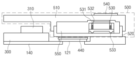
도 6은 일 실시 예에 따른 연성 회로 기판을 포함하는 전자 장치의 내부를 도시한 것으로, 도 5의 A-A’ 단면을 나타내는 도면이다.FIG. 6 is a drawing illustrating the interior of an electronic device including a flexible circuit board according to one embodiment, taken along the line A-A’ of FIG. 5.
도 6을 참조하면, 일 실시 예에서, 전자 장치는 메인 회로 기판(200), 배터리(159), 및 연성 회로 기판(400)를 포함할 수 있다.Referring to FIG. 6, in one embodiment, the electronic device may include a main circuit board (200), a battery (159), and a flexible circuit board (400).
일 실시 예에 따르면, 메인 회로 기판(200)은 제1 메인 회로 기판(210)(또는 마스터 회로 기판) 및 제2 메인 회로 기판(220)(또는 슬레이브 회로 기판)을 포함할 수 있다. 도 6를 참조하면, 메인 회로 기판(200)은 제1 메인 회로 기판(210) 및 제2 메인 회로 기판(220) 만을 포함하는 것으로 도시되나, 이는 예시에 불과하고 적층되는 회로 기판의 개수는 도 6에 도시된 실시 예에 한정되지 않는다. According to one embodiment, the main circuit board (200) may include a first main circuit board (210) (or master circuit board) and a second main circuit board (220) (or slave circuit board). Referring to FIG. 6, the main circuit board (200) is illustrated as including only the first main circuit board (210) and the second main circuit board (220), but this is merely an example and the number of circuit boards to be stacked is not limited to the embodiment illustrated in FIG. 6.
일 실시 예에 따르면, 메인 회로 기판(200)은 제1 메인 회로 기판(210), 제2 메인 회로 기판(220) 및, 인터포저(interposer)(201)를 포함할 수 있다. According to one embodiment, the main circuit board (200) may include a first main circuit board (210), a second main circuit board (220), and an interposer (201).
일 실시 예에 따르면, 제1 메인 회로 기판(210)은 프로세서(232)를 포함할 수 있다. 예를 들어, 프로세서(232)는 제1 메인 회로 기판(210) 및 제2 메인 회로 기판(220) 사이에서, 인터포저(interposer)(201)에 의해서 형성되는 공간에 위치할 수 있다. 예를 들어, 제1 커넥터(401)는 제2 메인 회로 기판(220)과 연성 회로 기판(400)의 메인 영역(410)을 연결할 수 있다. 일 실시 예에 따르면, 제1 메인 회로 기판(210)은 배터리(159)의 제1 측면(1591)과 마주보도록 배치될 수 있다. According to one embodiment, the first main circuit board (210) may include a processor (232). For example, the processor (232) may be located in a space formed by an interposer (201) between the first main circuit board (210) and the second main circuit board (220). For example, the first connector (401) may connect the second main circuit board (220) and the main area (410) of the flexible circuit board (400). According to one embodiment, the first main circuit board (210) may be arranged to face the first side (1591) of the battery (159).
일 실시 예에 따르면, 제2 메인 회로 기판(220)은 RF 회로(231) 및 제2 커넥터(401)를 포함할 수 있다. 제2 메인 회로 기판(220)은 배터리(159)의 제1 측면(1591)과 마주보도록 배치될 수 있다. According to one embodiment, the second main circuit board (220) may include an RF circuit (231) and a second connector (401). The second main circuit board (220) may be positioned to face the first side (1591) of the battery (159).
일 실시 예에 따르면, 인터포저(interposer)(201)는 메인 회로 기판(200)이 적층 구조를 가질 수 있도록, 전기적 및/또는 물리적으로 제1 메인 회로 기판(210)과 제2 메인 회로 기판(220)을 연결할 수 있다. According to one embodiment, an interposer (201) may electrically and/or physically connect a first main circuit board (210) and a second main circuit board (220) such that the main circuit board (200) may have a laminated structure.
일 실시 예에 따르면, 배터리(159)는 제1 측면(1591), 제2 측면(1592), 제1 면(1593) 및 제2 면(1594)를 포함할 수 있다. According to one embodiment, the battery (159) may include a first side (1591), a second side (1592), a first side (1593), and a second side (1594).
일 실시 예에 따르면, 제1 측면(1591)은 제2 측면(1592)과 대향하고, 제1 메인 회로 기판(210) 및 제2 메인 회로 기판(220)과 마주볼 수 있다. 제2 측면(1592)는 제1 측면(1591)과 대향하고, 연성 회로 기판(400)의 굴절 영역(422)과 마주볼 수 있다. 제1 면(1593)은 연성 회로 기판(400)의 메인 영역(410)과 마주보며, 배터리(159)의 상부(예: 도면을 기준으로 상부)면을 형성할 수 있다. 제2 면(1594)는 제1 면(1593)과 대향하고, 배터리(159)의 하부(예: 도면을 기준으로 하부)면을 형성할 수 있다.According to one embodiment, the first side (1591) may be opposite the second side (1592) and may face the first main circuit board (210) and the second main circuit board (220). The second side (1592) may be opposite the first side (1591) and may face the flexure region (422) of the flexible circuit board (400). The first side (1593) may be opposite the main region (410) of the flexible circuit board (400) and may form an upper (e.g., upper based on the drawing) surface of the battery (159). The second side (1594) may be opposite the first side (1593) and may form a lower (e.g., lower based on the drawing) surface of the battery (159).
일 실시 예에 따르면, 연성 회로 기판(400)은, 메인 영역(410), 제1 분기 영역(420), 벤딩 부분(421), 및 굴절 영역(422)을 포함할 수 있다. According to one embodiment, the flexible circuit board (400) may include a main region (410), a first branch region (420), a bending portion (421), and a bending region (422).
일 실시 예에 따르면, 메인 영역(410)은, 메인 영역(410)으로부터 제1 분기 영역(420) 및 제2 분기 영역(미도시)(예:도 5의 제2 분기 영역(430))으로 분기되는 부분(411)을 포함할 수 있다. 분기되는 부분(411)는 배터리(159)의 제1 면(1593)의 적어도 일부와 마주보도록 메인 영역(410)에 형성될 수 있다. 일 실시 예에 따르면, 메인 영역(410)은 일 단부에 부착재(202)가 결합될 수 있다. 예를 들어, 부착재(202)는 SUS 프레임을 포함하는 보강판을 포함할 수 있다. According to one embodiment, the main region (410) may include a portion (411) branching from the main region (410) into a first branch region (420) and a second branch region (not shown) (e.g., the second branch region (430) of FIG. 5). The branching portion (411) may be formed in the main region (410) so as to face at least a portion of the first surface (1593) of the battery (159). According to one embodiment, the main region (410) may have an attachment (202) coupled to one end. For example, the attachment (202) may include a reinforcing plate including a SUS frame.
일 실시 예에 따르면, 제1 분기 영역(420)은 벤딩 부분(421) 및 굴절 영역(422)를 포함할 수 있다. According to one embodiment, the first branch region (420) may include a bending portion (421) and a bending region (422).
일 실시 예에 따르면, 벤딩 부분(421)은 배터리(159)를 감싸는 방향으로 구부러지도록 형성될 수 있다. 어떤 실시 예에서, 벤딩 부분(421)은 제1 분기 영역(420)이 배터리(159)의 제1 면(1593)과 마주 보도록 연장되는 방향에 대해서 수직한 방향으로 벤딩되는 부분을 포함할 수 있다. 벤딩 부분(421)은 메인 영역(410)과 굴절 영역(422)의 사이에 위치할 수 있다. 예를 들어, 벤딩 부분(421)은 일 측이 메인 영역(410)에 연결되고, 타 측이 굴절 영역(422)에 연결될 수 있다. According to one embodiment, the bending portion (421) may be formed to bend in a direction that surrounds the battery (159). In some embodiments, the bending portion (421) may include a portion that bends in a direction perpendicular to a direction in which the first branch region (420) extends to face the first side (1593) of the battery (159). The bending portion (421) may be positioned between the main region (410) and the bending region (422). For example, the bending portion (421) may have one side connected to the main region (410) and the other side connected to the bending region (422).
일 실시 예에 따르면, 굴절 영역(422)는 배터리(159)의 제2 측면(1592)와 마주보도록 배치될 수 있다. 예를 들어, 굴절 영역(422)의 크기는 배터리(159)의 제2 측면(1592)의 크기(예: 배터리(159)의 높이 또는 두께)에 대응하도록 설계될 수 있다. According to one embodiment, the bending region (422) may be positioned to face the second side (1592) of the battery (159). For example, the size of the bending region (422) may be designed to correspond to the size of the second side (1592) of the battery (159) (e.g., the height or thickness of the battery (159)).
일 실시 예에 따르면, 연성 회로 기판(400)은 메인 영역(410)으로부터 배터리(159)의 제1 면(1593)에 마주보며 X 방향으로 연장되는 배터리 상부 연장 영역(424) 및 배터리 상부 연장 영역(424)으로부터 ?Y 방향으로 연장되는 굴절 영역(422)를 포함할 수 있다. 연성 회로 기판(400)은 X 방향으로 연장되는 배터리 상부 연장 영역(424)과 ?Y 방향으로 연장되는 굴절 영역(422)을 연결하는 벤딩 부분(421)을 포함할 수 있다. 예를 들어, 벤딩 부분(421)는 연성 회로 기판(400)의 적어도 일부가 연장되는 방향이 바뀌도록 구부러지는 플렉서블한 부분을 포함할 수 있다. 일 실시 예에 따르면, 연성 회로 기판(400)의 제1 분기 영역(420) 중에서, 배터리(159)의 제2 측면(1592)과 마주보도록 배치되는 부분은 굴절 영역(422)으로 정의될 수 있다. 연성 회로 기판(400)의 굴절 영역(422)의 크기(또는 높이)는 배터리(159)의 제2 측면(1592)의 크기(예를 들어, 배터리의 두께)에 대응할 수 있다. 굴절 영역(422)은 벤딩 부분(421)으로부터 연장될 수 있다. 어떤 실시 예에서, 굴절 영역(422)은 배터리(159)의 제1 면(1593)에 수직하는 제2 측면(1592)과 마주보도록 배치될 수 있다. According to one embodiment, the flexible circuit board (400) may include a battery upper extension region (424) extending in the X direction from the main region (410) and facing the first side (1593) of the battery (159), and a bend region (422) extending in the -Y direction from the battery upper extension region (424). The flexible circuit board (400) may include a bend portion (421) connecting the battery upper extension region (424) extending in the X direction and the bend region (422) extending in the -Y direction. For example, the bend portion (421) may include a flexible portion that is bent so that at least a portion of the flexible circuit board (400) changes an extending direction. According to one embodiment, among the first branch regions (420) of the flexible circuit board (400), a portion that is arranged to face the second side (1592) of the battery (159) may be defined as the bend region (422). The size (or height) of the bending region (422) of the flexible circuit board (400) may correspond to the size of the second side (1592) of the battery (159) (e.g., the thickness of the battery). The bending region (422) may extend from the bending portion (421). In some embodiments, the bending region (422) may be positioned to face the second side (1592) which is perpendicular to the first side (1593) of the battery (159).
일 실시 예에 따르면, 연성 회로 기판(400)은 벤딩 부분(421)을 포함하므로, 전자 장치의 내부의 협소한 공간에 배치될 수 있다. 일 실시 예에 따르면, 연성 회로 기판(400)은 구부러질 수 있는 벤딩 부분(421)을 포함하므로, 전자 장치는 내부에 배치되는 컴포넌트(예를 들어: 배터리(159) 또는 스피커 모듈(예: 도 5의 스피커 모듈(500)))에 더 많은 공간을 할당할 수 있다. According to one embodiment, since the flexible circuit board (400) includes a bending portion (421), it can be placed in a narrow space inside an electronic device. According to one embodiment, since the flexible circuit board (400) includes a bendable bending portion (421), the electronic device can allocate more space to components placed inside it (e.g., a battery (159) or a speaker module (e.g., a speaker module (500) of FIG. 5)).
도 7은 일 실시 예에 따른 연성 회로 기판의 효과를 설명하기 위한 도면이다.FIG. 7 is a drawing for explaining the effect of a flexible circuit board according to one embodiment.
일 실시 예에 따르면, 연성 회로 기판(400)은 배터리(159)의 크기(또는 길이)에 따라서 설계될 수 있다. According to one embodiment, the flexible circuit board (400) can be designed according to the size (or length) of the battery (159).
예를 들어, 전자 장치는 고용량의 전력을 전자 장치에 공급하기 위해서 상대적으로 크기가 큰 배터리(159)를 포함할 수 있다. 도 7에 도시된 것처럼, 배터리(159)의 크기가 상대적으로 커지면, 이에 대응하여 제1 분기 영역(420) 또는 메인 영역(410)의 크기(또는 길이)가 상대적으로 증가되도록 설계될 수 있다. 다른 예에서, 배터리(159)의 높이 또는 두께(제2 측면(1592)의 크기 또는 길이)가 상대적으로 커지면, 이에 대응하여 굴절 영역(422)의 크기가 상대적으로 증가되도록 설계될 수 있다. For example, an electronic device may include a relatively large battery (159) to supply a large amount of power to the electronic device. As illustrated in FIG. 7, when the size of the battery (159) becomes relatively large, the size (or length) of the first branch region (420) or the main region (410) may be designed to increase relatively accordingly. In another example, when the height or thickness (the size or length of the second side (1592)) of the battery (159) becomes relatively large, the size of the refracted region (422) may be designed to increase relatively accordingly.
일 실시 예에 따른 전자 장치는 제한된 크기의 내부 공간을 가질 수 있다. 전자 장치의 내부 공간에는 복수의 컴포넌트들(예: 배터리(159) 및 스피커 모듈(미도시)(도 5의 스피커 모듈))이 배치될 수 있다. 일 실시 예에 따른 연성 회로 기판(400)은 벤딩 부분(421)을 포함하므로, 연성 회로 기판(400)은 제한된 크기를 갖는 전자 장치의 내부 공간에 효율적으로 배치될 수 있다.An electronic device according to an embodiment may have an internal space of a limited size. A plurality of components (e.g., a battery (159) and a speaker module (not shown) (speaker module of FIG. 5)) may be arranged in the internal space of the electronic device. Since a flexible circuit board (400) according to an embodiment includes a bending portion (421), the flexible circuit board (400) may be efficiently arranged in an internal space of an electronic device having a limited size.
도 8은 일 실시 예에 따른 연성 회로 기판을 포함하는 전자 장치의 내부를 도시한 것으로, 도 5의 A-A’ 단면을 나타내는 도면이다.FIG. 8 is a drawing illustrating the interior of an electronic device including a flexible circuit board according to one embodiment, taken along the line A-A’ of FIG. 5.
일 실시 예에 따르면, 연성 회로 기판(400)은 메인 영역(410), 메인 영역에 형성되는 분기되는 부분(411)으로부터 연장되는 제1 분기 영역(420), 메인 영역에 형성되는 분기되는 부분(411)으로부터 연장되는 제2 분기 영역(미도시)(예: 도 5의 제2 분기 영역(430))을 포함할 수 있다. According to one embodiment, the flexible circuit board (400) may include a main region (410), a first branch region (420) extending from a branching portion (411) formed in the main region, and a second branch region (not shown) extending from the branching portion (411) formed in the main region (e.g., the second branch region (430) of FIG. 5).
일 실시 예에 따르면, 제1 분기 영역(420)은 벤딩 부분(421) 및 굴절 영역(422)를 포함할 수 있다. According to one embodiment, the first branch region (420) may include a bending portion (421) and a bending region (422).
일 실시 예에 따르면, 제1 분기 영역(420)은, 제1 단부(4201)가 분기되는 부분(411)에 연결되고, 제2 단부(4202)는 외부 인터페이스 부재(440)와 전기적 및/또는 물리적으로 연결될 수 있다. 예를 들어, 제1 분기 영역(420)의 적어도 일부는, 배터리(159)의 제1 면(1593)과 마주보도록 형성될 수 있다. According to one embodiment, the first branch region (420) may be connected to the portion (411) where the first end (4201) branches, and the second end (4202) may be electrically and/or physically connected to the external interface member (440). For example, at least a portion of the first branch region (420) may be formed to face the first side (1593) of the battery (159).
일 실시 예에 따르면, 벤딩 부분(421)은 배터리(159) 및 스피커 모듈(500)의 사이에 배치되는 굴절 영역(422)의 양 측에 각각 형성될 수 있다. 예를 들어, 벤딩 부분(421)은 배터리(159)를 감싸는 방향으로 벤딩되는 부분을 포함할 수 있다. 예를 들어, 벤딩 부분(421)은 스피커 하부 인클로저(520)를 감싸는 방향으로 벤딩되는 부분을 포함할 수 있다. 일 실시 예에 따르면, 스피커 하부 인클로저(520)의 적어도 일부가 외부 인터페이스 부재(440)의 적어도 일부와 물리적으로 접촉할 수 있다. 외부 인터페이스 부재(440)가 스피커 하부 인클로저(520)의 적어도 일부와 접촉함으로써, 외부 인터페이스 부재(440)의 움직임이 최소화되도록 외부 인터페이스 부재(440)가 고정될 수 있다. According to one embodiment, the bending portion (421) may be formed on each side of the bending region (422) disposed between the battery (159) and the speaker module (500). For example, the bending portion (421) may include a portion that bends in a direction that surrounds the battery (159). For example, the bending portion (421) may include a portion that bends in a direction that surrounds the speaker lower enclosure (520). According to one embodiment, at least a portion of the speaker lower enclosure (520) may be in physical contact with at least a portion of the external interface member (440). By making contact with at least a portion of the speaker lower enclosure (520), the external interface member (440) may be fixed so that movement of the external interface member (440) is minimized.
일 실시 예에 따르면, 굴절 영역(422)은 배터리(159) 및 스피커 모듈(500)의 사이에 배치될 수 있다. 어떤 예에서, 굴절 영역(422)는 배터리(159)의 제1 면(1593)에 수직하도록 형성된 배터리(159)의 제2 측면(1592)과 마주보도록 형성될 수 있다. According to one embodiment, the refracting region (422) may be positioned between the battery (159) and the speaker module (500). In some examples, the refracting region (422) may be formed to face the second side (1592) of the battery (159), which is formed to be perpendicular to the first side (1593) of the battery (159).
도 9는 일 실시 예에 따른 연성 회로 기판을 포함하는 전자 장치의 내부를 도시한 것으로, 도 5의 B-B’ 단면을 나타내는 도면이다.FIG. 9 is a drawing illustrating the interior of an electronic device including a flexible circuit board according to one embodiment, taken along the line B-B’ of FIG. 5.
일 실시 예에 따른 전자 장치(예: 도 1 내지 도 3의 전자 장치(100), 도 5의 전자 장치(100))는 서브 회로 기판(300), 스피커 모듈(500), 브라켓(140), 스티프너(stiffener)(121), 및 외부 인터페이스 부재(440)를 포함할 수 있다.An electronic device according to one embodiment (e.g., the electronic device (100) of FIGS. 1 to 3, the electronic device (100) of FIG. 5) may include a sub-circuit board (300), a speaker module (500), a bracket (140), a stiffener (121), and an external interface member (440).
일 실시 예에 따르면, 서브 회로 기판(300)은 접속 회로(310)를 포함할 수 있다. 서브 회로 기판(300)은 브라켓(140)의 적어도 일부와 연결될 수 있다. 접속 회로(310)는 스피커 상부 인클로저(510)과 서브 회로 기판(300)의 사이에 배치될 수 있다. According to one embodiment, the sub-circuit board (300) may include a connection circuit (310). The sub-circuit board (300) may be connected to at least a portion of the bracket (140). The connection circuit (310) may be positioned between the speaker upper enclosure (510) and the sub-circuit board (300).
일 실시 예에 따르면, 스피커 모듈(500)은 스피커 상부 인클로저(510), 스피커 하부 인클로저(520) 및 스피커 코어(530)를 포함할 수 있다. According to one embodiment, the speaker module (500) may include a speaker upper enclosure (510), a speaker lower enclosure (520), and a speaker core (530).
일 실시 예에 따르면, 스피커 상부 인클로저(510)는 적어도 하나의 LDS(Laser Direct Structure) 안테나(540)를 더 포함할 수 있다. 스피커 상부 인클로저(510)는, 내부에 스피커 코어(530) 및 공명 공간을 포함하도록 스피커 하부 인클로저(520)와 연결될 수 있다. According to one embodiment, the speaker upper enclosure (510) may further include at least one LDS (Laser Direct Structure) antenna (540). The speaker upper enclosure (510) may be connected to the speaker lower enclosure (520) to include a speaker core (530) and a resonant space therein.
일 실시 예에 따르면, 스피커 하부 인클로저(520)는 브라켓(140)의 적어도 일부와 연결될 수 있다. 스피커 하부 인클로저(520)와 스티프너(121)의 사이에, 외부 인터페이스 부재(440)가 배치될 수 있다. 일 실시 예에 따르면, 스티프너(121)는 상대적으로 두께가 얇은 연성 회로 기판의 두께를 보강하기 위해서, 연성 회로 기판의 아래에 배치될 수 있다. 예를 들어 스티프너(121)는, 외부 인터페이스 부재(440)가 움직이는 경우, 주변 구조물(예: 브라켓)에 생길 수 있는 손상을 방지하기 위하여 외부 인터페이스 부재(440)의 적어도 일부와 연결되도록 배치될 수 있다.In one embodiment, the speaker lower enclosure (520) may be connected to at least a portion of the bracket (140). An external interface member (440) may be disposed between the speaker lower enclosure (520) and the stiffener (121). In one embodiment, the stiffener (121) may be disposed below the flexible circuit board to reinforce the thickness of the relatively thin flexible circuit board. For example, the stiffener (121) may be disposed to be connected to at least a portion of the external interface member (440) to prevent damage to a surrounding structure (e.g., the bracket) when the external interface member (440) moves.
일 실시 예에 따르면, 스피커 코어(530)는 자성 물질(예를 들어 자석(magnet)), 코일(531)(coil) 및 요크(532)(yoke)를 포함할 수 있다. 스피커 `코어(530)는 자성 물질 및 코일(531)을 이용하여 생성된 떨림을 공명 공간에서 증폭시킬 수 있다. 일 실시 예에 따르면, 스피커 모듈(500)는 공명 체적(Speaker Volume, 550)을 포함할 수 있다. 예를 들어, 공명 체적을 이용하여 스피커 모듈(500)의 음압과 오디오 주파수의 공진 특성이 조정될 수 있다.According to one embodiment, the speaker core (530) may include a magnetic material (e.g., a magnet), a coil (531) and a yoke (532). The speaker core (530) may amplify vibrations generated by using the magnetic material and the coil (531) in a resonant space. According to one embodiment, the speaker module (500) may include a resonant volume (Speaker Volume, 550). For example, the resonant volume may be used to adjust the sound pressure and resonance characteristics of audio frequencies of the speaker module (500).
일 실시 예에 따르면, 브라켓(140)은 외부로 노출되는 개구부(opening)를 형성할 수 있다. 개구부(opening)와 외부 인터페이스 부재(440)의 사이에는 스티프너(121)가 배치될 수 있다. 일 실시 예에 따르면, 브라켓(140)의 적어도 일부에 서브 회로 기판(300)이 배치될 수 있다. According to one embodiment, the bracket (140) may form an opening that is exposed to the outside. A stiffener (121) may be arranged between the opening and the external interface member (440). According to one embodiment, a sub-circuit board (300) may be arranged on at least a portion of the bracket (140).
일 실시 예에 따르면, 스티프너(121)는 브라켓(140)의 적어도 일부와 연결 될 수 있다. 스티프너(121)는 외부 인터페이스 부재(440)와 연결될 수 있다. 스티프너(121)(stiffener)의 적어도 일부가 개구부(opening)와 연결됨에 따라, 개구부를 형성하는 브라켓(140)의 강도가 높아질 수 있다.According to one embodiment, the stiffener (121) can be connected to at least a portion of the bracket (140). The stiffener (121) can be connected to the external interface member (440). As at least a portion of the stiffener (121) is connected to the opening, the strength of the bracket (140) forming the opening can be increased.
일 실시 예에 따르면, 외부 인터페이스 부재(440)는 스피커 하부 인클로저(520)의 하부(예: 도면을 기준으로 아래)에 배치될 수 있다. 예를 들어, 외부 인터페이스 부재(440)의 적어도 일부가 개구부(opening)를 통해서 전자 장치의 외부로 노출될 수 있다. 예를 들어, 외부 인터페이스 부재(440)의 하부에 스티프너(121)가 연결될 수 있다. According to one embodiment, the external interface member (440) may be positioned at the bottom (e.g., below with respect to the drawing) of the speaker lower enclosure (520). For example, at least a portion of the external interface member (440) may be exposed to the outside of the electronic device through an opening. For example, a stiffener (121) may be connected to the bottom of the external interface member (440).
도 10은 일 실시 예에 따른 전자 장치의 내부 구조를 도시한 단면도이다. FIG. 10 is a cross-sectional view illustrating the internal structure of an electronic device according to one embodiment.
도 10을 참조하면, 전자 장치(예: 도 1 내지 도 3의 전자 장치(100), 도 5의 전자 장치)는 전면 플레이트(120), 후면 플레이트(180) 및 브라켓(140)을 포함할 수 있다. 다른 실시 예에서, 전면 플레이트(120)는 디스플레이(예: 도 3의 디스플레이(130))에 포함된 커버 레이어로 참조될 수 있다. 어떤 실시 예에서, 전면 플레이트(120)는 제1 커버로 참조될 수 있고, 후면 플레이트(180)는 제2 커버로 참조될 수 있다. Referring to FIG. 10, an electronic device (e.g., the electronic device (100) of FIGS. 1 to 3, the electronic device of FIG. 5) may include a front plate (120), a rear plate (180), and a bracket (140). In another embodiment, the front plate (120) may be referred to as a cover layer included in a display (e.g., the display (130) of FIG. 3). In some embodiments, the front plate (120) may be referred to as a first cover, and the rear plate (180) may be referred to as a second cover.
일 실시 예에서, 브라켓(140)은 전면 플레이트(120)와 후면 플레이트(180)의 사이에서, 전면 플레이트(120)와 후면 플레이트(180)의 외측면을 둘러싸는 프레임 구조(1401), 및 프레임 구조(1401)로부터 하우징(예: 도 5의 하우징(110)의 내측으로 연장되는 플레이트 구조(1402)를 포함할 수 있다. 다른 실시 예에서, 플레이트 구조(1402)는 프레임 구조(1401)와 서로 다른 재질로 형성될 수 있고, 프레임 구조(1401)와 일체로 형성될 수 있다. 일 실시 예에서, 플레이트 구조(1402) 및 프레임 구조(1401)는 서로 다른 재질로 구성될 수 있고, 함께 용접 결합될 수 있다. In one embodiment, the bracket (140) may include a frame structure (1401) surrounding the outer surfaces of the front plate (120) and the rear plate (180) between the front plate (120) and the rear plate (180), and a plate structure (1402) extending from the frame structure (1401) toward the inside of the housing (e.g., the housing (110) of FIG. 5). In another embodiment, the plate structure (1402) may be formed of a different material from the frame structure (1401) and may be formed integrally with the frame structure (1401). In one embodiment, the plate structure (1402) and the frame structure (1401) may be formed of different materials and may be welded together.
일 실시 예에서, 프레임 구조(1401)는 전면 플레이트(120) 및 후면 플레이트(180)와 연결될 수 있다. 예를 들어, 프레임 구조(1401)는 전면 플레이트(120) 및 후면 플레이트(180)와 결합될 수 있다. 예를 들어, 프레임 구조(1401)에는 전면 플레이트(120) 및 후면 플레이트(180)가 각각 안착될 수 있다. 일 실시 예에서, 프레임 구조(1401)에는 프레임 구조(1401)를 관통하는 오프닝(149)이 형성될 수 있다. 상기 오프닝(149)의 내부에는 외부 인터페이스 부재(440)의 적어도 일부가 배치될 수 있다. 외부 인터페이스 부재(440)는 상기 오프닝(149)을 통해 외부의 다른 전자 장치와 전기적으로 연결될 수 있다. In one embodiment, the frame structure (1401) can be connected to the front plate (120) and the back plate (180). For example, the frame structure (1401) can be combined with the front plate (120) and the back plate (180). For example, the front plate (120) and the back plate (180) can be respectively mounted on the frame structure (1401). In one embodiment, the frame structure (1401) can have an opening (149) formed therethrough. At least a portion of an external interface member (440) can be disposed inside the opening (149). The external interface member (440) can be electrically connected to another external electronic device through the opening (149).
일 실시 예에서, 플레이트 구조(1402)의 제2 면(140b)에는 전면 플레이트(120)가 배치되고, 제1 면(140a)에는 메인 회로 기판(200), 배터리(159), 스피커 모듈(500), 외부 인터페이스 부재(440)가 배치될 수 있다. In one embodiment, a front plate (120) may be arranged on a second side (140b) of the plate structure (1402), and a main circuit board (200), a battery (159), a speaker module (500), and an external interface member (440) may be arranged on a first side (140a).
일 실시 예에서, 플레이트 구조(1402)는 배터리(159)를 고정시키기 위한 프레임 월(143)을 포함할 수 있다. 예를 들어, 프레임 월(143)은 플레이트 구조(1402)의 제1 면(140a)으로부터 연장될 수 있다, In one embodiment, the plate structure (1402) may include a frame wall (143) for fixing the battery (159). For example, the frame wall (143) may extend from a first side (140a) of the plate structure (1402).
일 실시 예에서, 프레임 월(143)은 배터리(159)의 적어도 일부를 둘러쌀 수 있다. 예를 들어, 프레임 월(143)은 스피커 모듈(500)에 인접한 제1 부분(1431), 및 메인 회로 기판(200)에 인접한 제2 부분(1432)을 포함할 수 있다. 일 실시 예에서, 제1 부분(1431)은 연성 회로 기판(400)의 굴절 영역(422)과 마주볼 수 있다. 예를 들어, 제1 부분(1431)과 스피커 모듈(500) 사이에는 연성 회로 기판(400)의 굴절 영역(422)의 일부가 위치될 수 있다. In one embodiment, the frame wall (143) can surround at least a portion of the battery (159). For example, the frame wall (143) can include a first portion (1431) adjacent the speaker module (500) and a second portion (1432) adjacent the main circuit board (200). In one embodiment, the first portion (1431) can face the flexure region (422) of the flexible circuit board (400). For example, a portion of the flexure region (422) of the flexible circuit board (400) can be positioned between the first portion (1431) and the speaker module (500).
다른 실시 예에서, 전면 플레이트(120), 후면 플레이트(180), 및 브라켓(140)의 프레임 구조(1401)는 전자 장치(100)의 내부 공간을 형성하는 하우징 구조(예: 도 1의 하우징(110))를 형성할 수 있다. 이 때, 플레이트 구조(1402)는 전자 장치(100)의 구조물을 지지하는 지지 부재(예: 도 3의 제1 지지 구조(142))로 참조될 수 있다. In another embodiment, the frame structure (1401) of the front plate (120), the rear plate (180), and the bracket (140) may form a housing structure (e.g., the housing (110) of FIG. 1) that forms an internal space of the electronic device (100). At this time, the plate structure (1402) may be referred to as a support member (e.g., the first support structure (142) of FIG. 3) that supports the structure of the electronic device (100).
일 실시 예에서, 스피커 모듈(500)은 인클로저(510, 520), 및 인클로저(510, 520) 내부에 배치되는 스피커 코어(530)를 포함할 수 있다. 인클로저(510, 520)는 상부 인클로저(510)와 하부 인클로저(520)를 포함할 수 있다. 다양한 실시 예에서, 상부 인클로저(510)는 적어도 하나의 LDS(Laser Direct Structure) 안테나(540)를 더 포함할 수 있다.In one embodiment, the speaker module (500) may include an enclosure (510, 520) and a speaker core (530) disposed within the enclosure (510, 520). The enclosure (510, 520) may include an upper enclosure (510) and a lower enclosure (520). In various embodiments, the upper enclosure (510) may further include at least one LDS (Laser Direct Structure) antenna (540).
일 실시 예에서, 연성 회로 기판(400)은 굴절 영역(422)으로부터 연장되는 연장 영역(423)을 포함할 수 있다. 메인 영역(410)은 배터리(159)의 제1 면(1593)에 위치하고, 연장 영역(423)은 플레이트 구조(1402)의 제1 면(140a)에 위치될 수 있다. In one embodiment, the flexible circuit board (400) may include an extension region (423) extending from a bend region (422). The main region (410) may be located on a first side (1593) of the battery (159), and the extension region (423) may be located on a first side (140a) of the plate structure (1402).
일 실시 예에서, 연성 회로 기판(400)은 적어도 일부가 후면 플레이트(180)와 배터리(159) 사이에 위치되고, 다른 일부가 스피커 모듈(500)과 플레이트 구조(1402) 사이에 위치되도록 형성될 수 있다. 예를 들어, 연성 회로 기판(400)의 메인 영역(410)과 제1 분기 영역(420)의 일부는 배터리(159)의 제1 면(1593)과 후면 플레이트(180) 사이에 위치되고, 굴절 영역(422)으로부터 연장된 연장 영역(423)은 플레이트 구조(1402)의 제1 면(140a)과 스피커 모듈(500) 사이로 연장될 수 있다. 예를 들어, 연장 영역(423)은 외부 인터페이스 부재(440)에 연결될 수 있다. 일 실시 예에 따르면, 연장 영역(423)은 스피커 코어(530)와 중첩되도록 배치될 수 있다. 또는, 벤딩 부분(421)으로부터 연장되는 연장 영역(423)은 스피커 코어(530)가 배치된 위치와 중첩되도록 배치될 수 있고, 스피커 모듈(500)에서 생성된 소리가 전자 장치(100)의 외부로 출력되는 음향 홀(미도시)의 위치와 중첩되지 않도록 배치될 수 있다. In one embodiment, the flexible circuit board (400) can be formed such that at least a portion is positioned between the back plate (180) and the battery (159), and another portion is positioned between the speaker module (500) and the plate structure (1402). For example, a portion of the main region (410) and the first branch region (420) of the flexible circuit board (400) can be positioned between the first side (1593) of the battery (159) and the back plate (180), and an extension region (423) extending from the bend region (422) can extend between the first side (140a) of the plate structure (1402) and the speaker module (500). For example, the extension region (423) can be connected to the external interface member (440). According to one embodiment, the extension region (423) can be positioned to overlap the speaker core (530). Alternatively, the extension region (423) extending from the bending portion (421) may be positioned so as to overlap with the position where the speaker core (530) is positioned, and may be positioned so as not to overlap with the position of the sound hole (not shown) through which sound generated from the speaker module (500) is output to the outside of the electronic device (100).
예를 들어, 연성 회로 기판(400)의 벤딩 부분(421)은 배터리(159)의 제1 면(1593)의 가장자리에서 플레이트 구조(1402)의 제1 면(140a)을 향하도록 구부러질 수 있다. 연성 회로 기판(400)의 벤딩 부분(421)은 굴절 영역(422)으로부터 오프닝(149)을 향하도록 구부러질 수 있다. 연성 회로 기판(400)의 벤딩 부분(421)은 연장 부분(423)이 굴절 영역(422)으로부터 플레이트 구조(1402)의 제1 면(140a)과 스피커 모듈(500) 사이로 연장되도록 구부러질 수 있다. For example, the bending portion (421) of the flexible circuit board (400) can be bent from an edge of the first side (1593) of the battery (159) toward the first side (140a) of the plate structure (1402). The bending portion (421) of the flexible circuit board (400) can be bent from the bending area (422) toward the opening (149). The bending portion (421) of the flexible circuit board (400) can be bent such that the extension portion (423) extends from the bending area (422) between the first side (140a) of the plate structure (1402) and the speaker module (500).
일 실시 예에서, 연성 회로 기판(400)은 일부가 메인 회로 기판(200)으로부터 후면 플레이트(180)와 배터리(159)의 제1 면(1593) 사이의 공간을 통해 연장되고, 다른 일부가 스피커 모듈(500)과 배터리(159)의 제2 측면(1592) 사이의 공간으로 연장되도록, 상기 일부와 다른 일부를 연결하는 굴절 영역(422)을 포함할 수 있다. 예를 들어, 연성 회로 기판(400)의 굴절 영역(422)은 메인 영역(410)으로부터 스피커 모듈(500)과 배터리(159)의 제2 측면(1592) 사이로 연장될 수 있다. In one embodiment, the flexible circuit board (400) may include a flexure region (422) connecting a portion of the flexible circuit board (200) and another portion thereof such that a portion thereof extends from the main circuit board (200) through a space between the back plate (180) and the first side (1593) of the battery (159), and another portion thereof extends into a space between the speaker module (500) and the second side (1592) of the battery (159). For example, the flexure region (422) of the flexible circuit board (400) may extend from the main region (410) between the speaker module (500) and the second side (1592) of the battery (159).
일 실시 예에서, 메인 회로 기판(200)으로부터 외부 인터페이스 부재(440)까지 연장되는 방향을 연성 회로 기판(400)의 연장 방향으로 규정할 수 있다. 연성 회로 기판(400)의 연장 방향으로 볼 때, 굴절 영역(422)은 후면 플레이트(180)로부터 전면 플레이트(120)를 향하는 방향으로 연장될 수 있다. 다양한 실시 예에서, 굴절 영역(422)은 연성 회로 기판(400)의 연장 방향으로 볼 때, 전자 장치(100)의 후면으로부터 전면을 향하는 방향으로 연장될 수 있다. In one embodiment, the direction extending from the main circuit board (200) to the external interface member (440) can be defined as the extension direction of the flexible circuit board (400). When viewed in the extension direction of the flexible circuit board (400), the refractive region (422) can extend in a direction from the rear plate (180) toward the front plate (120). In various embodiments, the refractive region (422) can extend in a direction from the rear side of the electronic device (100) toward the front side when viewed in the extension direction of the flexible circuit board (400).
도 11은 다른 실시 예에 따른 전자 장치를 도시한 도면이다.FIG. 11 is a diagram illustrating an electronic device according to another embodiment.
도 11을 참조하면, 연성 회로 기판(예: 도 4의 연성 회로 기판(400))(1100)은 메인 영역(1110), 메인 영역(1110)으로부터 제1 분기 영역(1120)과 제2 분기 영역(1130)으로 분기되는 부분을 포함하는 슬릿 영역(1111), 슬릿 영역(1111)으로부터 제1 인터페이스 부재(1140), 제2 인터페이스 부재(1150)로 연장되는 제2 분기 영역(1130), 및 슬릿 영역(1111)으로부터 연장되고, 제2 분기 영역(1130)과 구별되는 제1 분기 영역(1120)을 포함할 수 있다. 예를 들어, 슬릿 영역(1111)으로부터 메인 영역(1110), 제1 분기 영역(1120) 및 제2 분기 영역(1130)은 각각 서로 다른 방향으로 연장될 수 있다. Referring to FIG. 11, a flexible circuit board (e.g., a flexible circuit board (400) of FIG. 4) (1100) may include a main region (1110), a slit region (1111) including a portion branching from the main region (1110) into a first branch region (1120) and a second branch region (1130), a second branch region (1130) extending from the slit region (1111) to a first interface member (1140) and a second interface member (1150), and a first branch region (1120) extending from the slit region (1111) and being distinct from the second branch region (1130). For example, the main region (1110), the first branch region (1120), and the second branch region (1130) may each extend in different directions from the slit region (1111).
일 실시 예에서, 연성 회로 기판(1100)은 메인 영역(1110), 및 제1 분기 영역(1120)은 전자 장치(예: 도 1 내지 도 3의 전자 장치(100) 또는 도 5의 전자 장치(100) 또는 도 10의 전자 장치(100) 또는 도 12의 전자 장치(2000))의 서로 이격된 컴포넌트들(예: 도 12의 제1 회로 기판(2100), 제2 회로 기판(2200))과 전기적으로 연결되도록 형성될 수 있다. In one embodiment, the flexible circuit board (1100) may be formed such that the main region (1110) and the first branch region (1120) are electrically connected to spaced apart components (e.g., the first circuit board (2100), the second circuit board (2200) of FIG. 12) of an electronic device (e.g., the electronic device (100) of FIG. 1 to FIG. 3 or the electronic device (100) of FIG. 5 or the electronic device (100) of FIG. 10 or the electronic device (2000) of FIG. 12).
일 실시 예에서, 메인 영역(1110)는 제1 커넥터(1101)를 포함할 수 있다. 제1 커넥터(1101)는 전자 장치(예: 도 12의 전자 장치(2000))의 내부에 배치되는 컴포넌트(예: 도 12의 제1 회로 기판(2100))와 전기적으로 연결될 수 있다. 예를 들어, 제1 커넥터(1101)는 전자 장치(예: 도 12의 전자 장치(2000))의 회로 기판(예: 도 12의 제1 회로 기판(2100))과 전기적으로 연결될 수 있다. 예를 들어, 제1 커넥터(1101)는 메인 영역(1110)의 단부에 배치될 수 있다. In one embodiment, the main region (1110) may include a first connector (1101). The first connector (1101) may be electrically connected to a component (e.g., a first circuit board (2100) of FIG. 12) disposed inside an electronic device (e.g., an electronic device (2000) of FIG. 12). For example, the first connector (1101) may be electrically connected to a circuit board (e.g., a first circuit board (2100) of FIG. 12) of the electronic device (e.g., an electronic device (2000) of FIG. 12). For example, the first connector (1101) may be disposed at an end of the main region (1110).
일 실시 예에서, 제1 분기 영역(1120)은 제2 커넥터(1102)를 포함할 수 있다. 제2 커넥터(1102)는 전자 장치(예: 도 12의 전자 장치(2000))의 내부에 배치되는 컴포넌트(예: 도 12의 제2 회로 기판(2200))와 전기적으로 연결될 수 있다. 예를 들어, 제2 커넥터(1102)는 전자 장치(예: 도 12의 전자 장치(2000))의 회로 기판(예: 도 12의 제2 회로 기판(2200))에 예를 들어, 제2 커넥터(1102)는 제1 분기 영역(1120)의 단부에 배치될 수 있다. In one embodiment, the first branch region (1120) can include a second connector (1102). The second connector (1102) can be electrically connected to a component (e.g., a second circuit board (2200) of FIG. 12) disposed inside an electronic device (e.g., an electronic device (2000) of FIG. 12). For example, the second connector (1102) can be disposed on a circuit board (e.g., a second circuit board (2200) of FIG. 12) of the electronic device (e.g., an electronic device (2000) of FIG. 12). For example, the second connector (1102) can be disposed at an end of the first branch region (1120).
일 실시 예에서, 제2 분기 영역(1130)에는 하나 이상의 인터페이스 부재(1140, 1150)가 결합될 수 있다. 예를 들어, 하나 이상의 인터페이스 부재(1140, 1150)는 제1 인터페이스 부재(1140), 및 제2 인터페이스 부재(1150)가 결합될 수 있다. 일 실시 예에서, 제1 인터페이스 부재(1140) 및 제2 인터페이스 부재(1150)는 각각 USB 리셉터클 또는 HDMI 커넥터 중에 어느 하나를 포함할 수 있다. 예를 들어, 제1 인터페이스 부재(1140)는 USB 리셉터클을 포함할 수 있고, 제2 인터페이스 부재(1150)는 HDMI 커넥터를 포함할 수 있다.In one embodiment, the second branch region (1130) may be coupled with one or more interface members (1140, 1150). For example, the one or more interface members (1140, 1150) may be coupled with a first interface member (1140) and a second interface member (1150). In one embodiment, the first interface member (1140) and the second interface member (1150) may each include one of a USB receptacle or an HDMI connector. For example, the first interface member (1140) may include a USB receptacle and the second interface member (1150) may include an HDMI connector.
일 실시 예에서, 제2 분기 영역(1130)는 전자 장치(예: 도 12의 전자 장치(2000))의 내부에서 구부러진 상태로 배치되는 벤딩 부분(1131)을 포함할 수 있다. In one embodiment, the second branch region (1130) may include a bending portion (1131) that is positioned in a bent state within an electronic device (e.g., electronic device (2000) of FIG. 12).
도 12는 다른 실시 예에 따른 전자 장치의 내부 구조를 도시한 도면이다.FIG. 12 is a drawing illustrating the internal structure of an electronic device according to another embodiment.
도 12를 참조하면, 전자 장치(2000)(예: 도1 내지 도 3의 전자 장치(100) 또는 도 5의 전자 장치(100) 또는 도 10의 전자 장치(100))는, 하우징(2010), 및 적어도 일부가 하우징(2010) 내부에 배치되는 컴포넌트들을 포함할 수 있다. 일 실시 예에서, 컴포넌트들은 제1 회로 기판(2100), 제2 회로 기판(2200), 연성 회로 기판(1100), 배터리(2500), 외부 인터페이스 부재(2340)(예: USB 리셉터클)(예: 도 11의 제1 인터페이스 부재(1140), 제2 인터페이스 부재(1150)), 및 스피커 코어(2410)를 포함하는 스피커 모듈(2400)을 포함할 수 있다. 일 실시 예에서, 외부 인터페이스 부재(2340)는 하우징(2010)의 표면에 형성된 오프닝(예: 도 10의 오프닝(149))을 통해 적어도 일부가 하우징(2010)의 외부로 노출되도록 배치될 수 있다. 다양한 실시 예에서, 도시된 전자 장치(2000)는 태블릿 형태의 모바일 전자 장치를 포함할 수 있다.Referring to FIG. 12, an electronic device (2000) (e.g., the electronic device (100) of FIGS. 1 to 3 or the electronic device (100) of FIG. 5 or the electronic device (100) of FIG. 10) may include a housing (2010) and components at least partially disposed inside the housing (2010). In one embodiment, the components may include a first circuit board (2100), a second circuit board (2200), a flexible circuit board (1100), a battery (2500), an external interface member (2340) (e.g., a USB receptacle) (e.g., the first interface member (1140), the second interface member (1150) of FIG. 11), and a speaker module (2400) including a speaker core (2410). In one embodiment, the external interface member (2340) may be positioned so that at least a portion of the member is exposed to the outside of the housing (2010) through an opening formed in a surface of the housing (e.g., opening (149) of FIG. 10). In various embodiments, the illustrated electronic device (2000) may include a mobile electronic device in the form of a tablet.
일 실시 예에서, 제1 회로 기판(2100) 및 제2 회로 기판(2200) 각각은 전자 회로(2110, 2210)를 포함할 수 있다. 예를 들어, 전자 회로(2110, 2210)는 데이터 통신을 수행하도록 구성되는 통신 회로, 배터리 충전 기능을 제공하는 충전 회로, 입출력 장치와 전기적으로 연결되는 접속 회로 중 적어도 하나를 포함할 수 있다. In one embodiment, each of the first circuit board (2100) and the second circuit board (2200) may include electronic circuits (2110, 2210). For example, the electronic circuits (2110, 2210) may include at least one of a communication circuit configured to perform data communication, a charging circuit providing a battery charging function, and a connection circuit electrically connected to an input/output device.
일 실시 예에서, 배터리(2500)는 제1 회로 기판(2100) 및 제2 회로 기판(2200) 사이에 배치될 수 있다. In one embodiment, the battery (2500) may be positioned between the first circuit board (2100) and the second circuit board (2200).
일 실시 예에서, 연성 회로 기판(1100)은 슬릿 영역(1111)이 배터리(2500)의 일 면과 마주보는 위치에 위치하도록 제1 회로 기판(2100)으로부터 제2 회로 기판(2200)까지 연장될 수 있다. 예를 들어, 연성 회로 기판(1100)은 메인 영역(1110)의 제1 커넥터(1101)가 제1 회로 기판(2100)에 결합되고 제1 분기 영역(1120)의 제2 커넥터(1102)가 제2 회로 기판(2200)에 결합되도록 배터리(2500)를 가로질러 연장될 수 있다. In one embodiment, the flexible circuit board (1100) can extend from the first circuit board (2100) to the second circuit board (2200) such that the slit region (1111) is positioned facing one side of the battery (2500). For example, the flexible circuit board (1100) can extend across the battery (2500) such that the first connector (1101) of the main region (1110) is coupled to the first circuit board (2100) and the second connector (1102) of the first branch region (1120) is coupled to the second circuit board (2200).
일 실시 예에서, 연성 회로 기판(1100)의 제2 분기 영역(1130)은 배터리(2500)의 일 면과 스피커 모듈(2400)의 일면의 사이의 공간으로 연장되는 벤딩 부분(1131), 및 벤딩 부분(1131)으로부터 연장되는 연장 영역(1132)을 포함할 수 있다. 벤딩 부분(1131)은 연장 영역(1132)의 적어도 일부가 스피커 모듈(2400)의 아래로 위치되도록 벤딩될 수 있다. 연장 영역(1132)의 일 단부에는 외부 인터페이스 부재(2340)가 배치될 수 있다. In one embodiment, the second branch region (1130) of the flexible circuit board (1100) may include a bending portion (1131) extending into a space between one side of the battery (2500) and one side of the speaker module (2400), and an extension region (1132) extending from the bending portion (1131). The bending portion (1131) may be bent such that at least a portion of the extension region (1132) is positioned below the speaker module (2400). An external interface member (2340) may be disposed at one end of the extension region (1132).
본 개시의 일 실시 예에 따른 전자 장치(예: 도1 내지 도 3의 전자 장치(100) 또는 도 5의 전자 장치(100) 또는 도 10의 전자 장치(100) 또는 도 12의 전자 장치(2000))는, 하우징(110), 상기 하우징 내부에 배치되는 메인 회로 기판(200), 상기 하우징 내부에 배치되고 상기 메인 회로 기판으로부터 이격 배치되는 서브 회로 기판(300), 상기 메인 회로 기판과 상기 서브 회로 기판 사이에 배치되는 배터리(159), 상기 배터리는 메인 기판과 마주보는 제1 측면(1591), 및 상기 제1 측면에 대향하며 서브 기판과 마주보는 제2 측면(1592)을 포함하고, 적어도 일부가 상기 하우징의 일 표면에 배치되고, 상기 전자 장치와 다른 전자 장치를 전기적으로 연결하기 위한 외부 인터페이스 부재(440), 및 상기 메인 회로 기판과 연결되는 연성 회로 기판(400)을 포함할 수 있다. 일 실시 예에 따르면, 상기 연성 회로 기판은, 상기 메인 회로 기판과 연결되는 메인 영역(410), 상기 메인 영역으로부터 상기 외부 인터페이스 부재와 연결되는 제1 분기 영역(420), 및 상기 메인 영역으로부터 상기 서브 회로 기판으로 연결되는 제2 분기 영역(430)을 포함하고, 상기 제1 분기 영역은 상기 배터리의 상기 제2 측면과 마주보도록 벤딩되는 벤딩 부분(421)을 포함할 수 있다.An electronic device according to an embodiment of the present disclosure (e.g., the electronic device (100) of FIGS. 1 to 3 or the electronic device (100) of FIG. 5 or the electronic device (100) of FIG. 10 or the electronic device (2000) of FIG. 12) may include a housing (110), a main circuit board (200) disposed inside the housing, a sub-circuit board (300) disposed inside the housing and spaced apart from the main circuit board, a battery (159) disposed between the main circuit board and the sub-circuit board, the battery including a first side (1591) facing the main board and a second side (1592) opposite to the first side and facing the sub-board, at least a portion of which is disposed on one surface of the housing and for electrically connecting the electronic device with another electronic device, and a flexible circuit board (400) connected to the main circuit board. According to one embodiment, the flexible circuit board includes a main region (410) connected to the main circuit board, a first branch region (420) connected from the main region to the external interface member, and a second branch region (430) connected from the main region to the sub circuit board, wherein the first branch region may include a bending portion (421) bent to face the second side of the battery.
일 실시 예에 따르면, 상기 전자 장치는 스피커 모듈(500)을 더 포함하고, 상기 벤딩 부분은, 상기 배터리의 일 측면과 상기 스피커 모듈의 일 측면의 사이에 배치될 수 있다.According to one embodiment, the electronic device further includes a speaker module (500), and the bending portion can be disposed between one side of the battery and one side of the speaker module.
일 실시 예에 따르면, 상기 전자 장치는 디스플레이(130)를 더 포함하고, 상기 하우징은, 상기 디스플레이가 노출되는 전면 및 상기 전면과 대향하며, 상기 스피커 모듈의 제1 측면과 마주 보는 후면을 포함하고, 상기 제1 분기 영역은, 상기 스피커 모듈의 제1 측면과 대향하는 상기 스피커 모듈의 제2 측면과 상기 전면의 사이로 연장될 수 있다.According to one embodiment, the electronic device further includes a display (130), and the housing includes a front surface where the display is exposed and a rear surface opposite the front surface and facing the first side surface of the speaker module, and the first branch region can extend between a second side surface of the speaker module opposite the first side surface of the speaker module and the front surface.
일 실시 예에 따르면, 상기 스피커 모듈(500)은, 상기 제1 측면의 적어도 일부에 LDS 안테나(540)가 배치될 수 있다.According to one embodiment, the speaker module (500) may have an LDS antenna (540) arranged on at least a portion of the first side.
일 실시 예에 따르면, 상기 배터리(159)는, 상기 제1 측면(1591) 및 상기 제2 측면(1592) 사이의 공간을 둘러싸고, 상기 하우징의 상기 후면과 마주보는 제3 측면(1593) 및 상기 제3 측면과 대향하며, 상기 하우징의 상기 전면과 마주보는 제4 측면(1594)을 포함하고, 상기 연성 회로 기판(400)은, 상기 제3 측면과 상기 하우징의 상기 후면의 사이에서, 상기 메인 영역으로부터 상기 제1 분기 영역 또는 제2 분기 영역 중에서 적어도 하나로 분기되는 슬릿 부분(411)을 포함할 수 있다.According to one embodiment, the battery (159) includes a third side (1593) surrounding a space between the first side (1591) and the second side (1592) and facing the rear surface of the housing, and a fourth side (1594) opposite the third side and facing the front surface of the housing, and the flexible circuit board (400) may include a slit portion (411) branching from the main region to at least one of the first branch region or the second branch region between the third side and the rear surface of the housing.
일 실시 예에 따르면, 상기 배터리(159)는, 상기 제1 측면(1591) 및 상기 제2 측면(1592) 사이의 공간을 둘러싸고, 상기 하우징의 상기 후면과 마주보는 제3 측면(1593) 및 상기 제3 측면과 대향하며, 상기 하우징의 상기 전면과 마주보는 제4 측면(1594)을 포함하고, 상기 연성 회로 기판(400)은, 상기 메인 영역으로부터 상기 제1 분기 영역 및/또는 제2 분기 영역으로 분기되는 슬릿 부분(411)을 포함하고, 상기 슬릿 부분은 상기 배터리의 상기 제3 측면(1593)의 적어도 일부와 마주 보도록 형성될 수 있다.According to one embodiment, the battery (159) includes a third side (1593) surrounding a space between the first side (1591) and the second side (1592) and facing the rear surface of the housing, and a fourth side (1594) opposite the third side and facing the front surface of the housing, and the flexible circuit board (400) includes a slit portion (411) branching from the main region into the first branch region and/or the second branch region, and the slit portion can be formed to face at least a portion of the third side (1593) of the battery.
일 실시 예에 따르면, 상기 연성 회로 기판(400)은, 상기 메인 영역과 상기 메인 회로 기판을 전기적으로 연결하는 제1 커넥터(401) 및 상기 제2 분기 영역과 상기 서브 회로 기판을 전기적으로 연결하는 제2 커넥터(402)를 더 포함할 수 있다. According to one embodiment, the flexible circuit board (400) may further include a first connector (401) electrically connecting the main region and the main circuit board, and a second connector (402) electrically connecting the second branch region and the sub circuit board.
일 실시 예에 따르면, 상기 메인 회로 기판(200)은, 데이터 통신을 수행하는 통신 회로 또는 상기 배터리를 충전하기 위한 충전 회로 중에서 적어도 하나(230)를 포함하고, 상기 서브 회로 기판(200)은, 상기 전자 장치에 대한 입출력 동작을 수행하는 입출력 회로(310)를 포함할 수 있다.According to one embodiment, the main circuit board (200) may include at least one (230) of a communication circuit for performing data communication or a charging circuit for charging the battery, and the sub-circuit board (200) may include an input/output circuit (310) for performing input/output operations for the electronic device.
일 실시 예에 따르면, 상기 제1 분기 영역(410)은, 상기 벤딩 부분(421)으로부터 연장되고, 상기 제2 측면(1592)과 마주보도록 배치되는 굴절 영역(422)을 포함하고, 상기 굴절 영역의 일 단부에 상기 외부 인터페이스 부재(440)가 연결될 수 있다.According to one embodiment, the first branch region (410) includes a bend region (422) extending from the bending portion (421) and positioned to face the second side (1592), and the external interface member (440) can be connected to one end of the bend region.
본 개시의 일 실시 예에 따른 전자 장치(예: 도1 내지 도 3의 전자 장치(100) 또는 도 5의 전자 장치(100) 또는 도 10의 전자 장치(100) 또는 도 12의 전자 장치(2000))는, 제1 커버(120), 상기 제1 커버에 대향하는 제2 커버(180), 및 상기 제1 커버와 상기 제2 커버 사이의 내부 공간을 둘러싸는 브라켓(140)을 포함하는 하우징 구조(110), 상기 브라켓은 상기 제1 커버와 상기 제2 커버를 연결하는 제1 구조(1401), 및 상기 제1 구조로부터 상기 내부 공간으로 연장되는 제2 구조(1402)를 포함하고, 상기 제2 구조와 상기 제2 커버 사이에 배치되는 배터리(159), 상기 제2 구조와 상기 제2 커버 사이에 배치되며 상기 배터리의 일 측(1591)에 배치되는 제1 회로 기판(200), 상기 제2 구조와 상기 제2 커버 사이에 배치되며 상기 배터리의 타 측(1592)에 배치되는 제2 회로 기판(300), 상기 제2 구조와 상기 제2 커버 사이에 배치되며 상기 배터리의 타 측에 배치되는 스피커 모듈(500), 및 상기 제1 회로 기판과 연결되는 연성 회로 기판(400), 상기 연성 회로 기판은 상기 배터리와 상기 제2 커버 사이에 배치되는 제1 부분(424), 상기 스피커 모듈과 상기 제2 구조 사이에 배치되는 제2 부분(423), 및 상기 제1 부분과 상기 제2 부분을 연결하는 제3 부분(422)을 포함하고, 상기 제3 부분은 적어도 일부가 상기 제1 부분으로부터 상기 제2 구조를 향하는 방향으로 연장될 수 있다.An electronic device according to an embodiment of the present disclosure (e.g., the electronic device (100) of FIGS. 1 to 3 or the electronic device (100) of FIG. 5 or the electronic device (100) of FIG. 10 or the electronic device (2000) of FIG. 12) comprises a housing structure (110) including a first cover (120), a second cover (180) facing the first cover, and a bracket (140) surrounding an internal space between the first cover and the second cover, the bracket including a first structure (1401) connecting the first cover and the second cover, and a second structure (1402) extending from the first structure into the internal space, a battery (159) disposed between the second structure and the second cover, a first circuit board (200) disposed between the second structure and the second cover and disposed on one side (1591) of the battery, a second circuit board (200) disposed between the second structure and the second cover and disposed on the other side of the battery. A second circuit board (300) disposed on a side (1592), a speaker module (500) disposed between the second structure and the second cover and disposed on the other side of the battery, and a flexible circuit board (400) connected to the first circuit board, the flexible circuit board including a first portion (424) disposed between the battery and the second cover, a second portion (423) disposed between the speaker module and the second structure, and a third portion (422) connecting the first portion and the second portion, wherein at least a portion of the third portion can extend from the first portion in a direction toward the second structure.
일 실시 예에 따르면, 상기 스피커 모듈(500)은 상기 제2 커버와 마주보는 일 측면의 적어도 일부에 LDS 안테나(540)가 배치될 수 있다.According to one embodiment, the speaker module (500) may have an LDS antenna (540) positioned on at least a portion of one side facing the second cover.
일 실시 예에 따르면, 상기 제3 부분의 길이는, 상기 배터리의 상기 일 측(1591) 또는 타 측(1592) 중에서 적어도 하나의 길이에 대응하도록 형성될 수 있다.According to one embodiment, the length of the third portion may be formed to correspond to the length of at least one of the one side (1591) or the other side (1592) of the battery.
일 실시 예에 따르면, 상기 제1 부분의 길이는, 상기 배터리의 상기 일 측과 상기 타 측을 연결하는 측면(1593)의 길이에 대응하도록 형성될 수 있다.According to one embodiment, the length of the first portion may be formed to correspond to the length of the side (1593) connecting the one side and the other side of the battery.
일 실시 예에 따르면, 상기 연성 회로 기판은, 상기 전자 장치와 다른 전자 장치를 전기적으로 연결하기 위한 외부 인터페이스 부재(440)를 더 포함하고, 상기 외부 인터페이스 부재는, 상기 제2 부분(423)으로부터 연장되어 상기 제2 부분의 일 단부와 결합될 수 있다.According to one embodiment, the flexible circuit board further includes an external interface member (440) for electrically connecting the electronic device with another electronic device, and the external interface member can extend from the second portion (423) and be coupled to one end of the second portion.
일 실시 예에 따르면, 상기 인터페이스 부재는, 상기 브라켓과 스크류(screw) 결합될 수 있다.According to one embodiment, the interface member may be screw-connected to the bracket.
일 실시 예에 따르면, 상기 제3 부분은, 상기 배터리의 타 측(1592)과 상기 스피커 모듈의 사이에 위치하는 굴절 영역(421) 및 상기 제1 부분과 상기 굴절 영역을 연결하는 벤딩 부분을 포함할 수 있다.According to one embodiment, the third portion may include a bending portion connecting the first portion and the bending portion and a bending region (421) positioned between the other side (1592) of the battery and the speaker module.
일 실시 예에 따르면, 상기 연성 회로 기판(400)은, 상기 제2 회로 기판으로 연결되는 제4 부분(430) 및 상기 제1 부분으로부터 상기 제4 부분으로 분기되는 슬릿 부분(411)을 포함할 수 있다.According to one embodiment, the flexible circuit board (400) may include a fourth portion (430) connected to the second circuit board and a slit portion (411) branching from the first portion to the fourth portion.
일 실시 예에 따르면, 상기 슬릿 부분(411)은, 상기 제2 커버(180) 및 상기 제2 커버와 마주보는 상기 배터리의 일 측면(1593)의 사이에 위치할 수 있다.According to one embodiment, the slit portion (411) may be located between the second cover (180) and one side (1593) of the battery facing the second cover.
일 실시 예에 따르면, 상기 제1 회로 기판은, 데이터 통신을 수행하는 통신 회로 또는 상기 배터리를 충전하기 위한 충전 회로 중에서 적어도 하나(230)를 포함하고, 상기 제2 회로 기판은, 상기 전자 장치에 대한 입출력 동작을 수행하는 입출력 회로(310)를 포함할 수 있다.According to one embodiment, the first circuit board may include at least one (230) of a communication circuit for performing data communication or a charging circuit for charging the battery, and the second circuit board may include an input/output circuit (310) for performing input/output operations for the electronic device.
일 실시 예에 따르면, 상기 전자 장치는 디스플레이(130)를 더 포함하고, 상기 디스플레이는 상기 제1 커버(120)의 적어도 일부를 통해서 노출될 수 있다.According to one embodiment, the electronic device further includes a display (130), wherein the display is exposed through at least a portion of the first cover (120).
본 문서의 다양한 실시 예들 및 이에 사용된 용어들은 본 문서에 기재된 기술을 특정한 실시 형태에 대해 한정하려는 것이 아니며, 해당 실시 예의 다양한 변경, 균등물, 및/또는 대체물을 포함하는 것으로 이해되어야 한다. 도면의 설명과 관련하여, 유사한 구성요소에 대해서는 유사한 참조 부호가 사용될 수 있다. 단수의 표현은 문맥상 명백하게 다르게 뜻하지 않는 한, 복수의 표현을 포함할 수 있다. 본 문서에서, "A 또는 B", "A 및/또는 B 중 적어도 하나", "A, B 또는 C" 또는 "A, B 및/또는 C 중 적어도 하나" 등의 표현은 함께 나열된 항목들의 모든 가능한 조합을 포함할 수 있다. "제1," "제2," "첫째," 또는 "둘째,"등의 표현들은 해당 구성요소들을, 순서 또는 중요도에 상관없이 수식할 수 있고, 한 구성요소를 다른 구성요소와 구분하기 위해 사용될 뿐 해당 구성요소들을 한정하지 않는다. 어떤(예: 제1) 구성요소가 다른(예: 제2) 구성요소에 "(기능적으로 또는 통신적으로) 연결되어" 있다거나 "접속되어" 있다고 언급된 때에는, 상기 어떤 구성요소가 상기 다른 구성요소에 직접적으로 연결되거나, 다른 구성요소(예: 제 3 구성요소)를 통하여 연결될 수 있다.The various embodiments of this document and the terminology used herein are not intended to limit the technology described in this document to the specific embodiments, but should be understood to encompass various modifications, equivalents, and/or substitutes of the embodiments. In connection with the description of the drawings, similar reference numerals may be used for similar components. The singular expressions may include plural expressions unless the context clearly indicates otherwise. In this document, expressions such as "A or B", "at least one of A and/or B", "A, B, or C" or "at least one of A, B and/or C" can include all possible combinations of the items listed together. Expressions such as "first," "second," "first," or "second" can modify the corresponding components, regardless of order or importance, and are only used to distinguish one component from another and do not limit the corresponding components. When it is said that a certain (e.g., a first) component is "(functionally or communicatively) connected" or "connected" to another (e.g., a second) component, said certain component may be directly connected to said other component, or may be connected through another component (e.g., a third component).
본 문서에서, "~하도록 설정된(adapted to or configured to)"은 상황에 따라, 예를 들면, 하드웨어적 또는 소프트웨어적으로 "~에 적합한," "~하는 능력을 가지는," "~하도록 변경된," "~하도록 만들어진," "~를 할 수 있는," 또는 "~하도록 설계된"과 상호 호환적으로(interchangeably) 사용될 수 있다. 어떤 상황에서는, "~하도록 구성된 장치"라는 표현은, 그 장치가 다른 장치 또는 부품들과 함께 "~할 수 있는" 것을 의미할 수 있다. 예를 들면, 문구 "A, B, 및 C를 수행하도록 설정된 (또는 구성된) 프로세서"는 해당 동작들을 수행하기 위한 전용 프로세서(예: 임베디드 프로세서), 또는 메모리 장치(예: 메모리 130)에 저장된 하나 이상의 프로그램들을 실행함으로써, 해당 동작들을 수행할 수 있는 범용 프로세서(예: CPU 또는 AP)를 의미할 수 있다.In this document, "adapted to or configured to" can be used interchangeably with, for example, "suitable for," "capable of," "modified to," "made to," "capable of," or "designed to," depending on the context, for example, hardware-wise or software-wise. In some contexts, the phrase "a device configured to" can mean that the device is "capable of" doing something together with other devices or components. For example, the phrase "a processor adapted (or configured) to perform A, B, and C" can mean a dedicated processor (e.g., an embedded processor) for performing the operations, or a general-purpose processor (e.g., a CPU or AP) that can perform the operations by executing one or more programs stored in a memory device (e.g., memory 130).
본 문서에서 사용된 용어 "모듈"은 하드웨어, 소프트웨어 또는 펌웨어(firmware)로 구성된 유닛(unit)을 포함하며, 예를 들면, 로직, 논리 블록, 부품, 또는 회로 등의 용어와 상호 호환적으로 사용될 수 있다. "모듈"은, 일체로 구성된 부품 또는 하나 또는 그 이상의 기능을 수행하는 최소 단위 또는 그 일부가 될 수 있다. "모듈"은 기계적으로 또는 전자적으로 구현될 수 있으며, 예를 들면, 어떤 동작들을 수행하는, 알려졌거나 앞으로 개발될, ASIC(application-specific integrated circuit) 칩, FPGAs(field-programmable gate arrays), 또는 프로그램 가능 논리 장치를 포함할 수 있다.The term "module" as used in this document includes a unit composed of hardware, software or firmware, and can be used interchangeably with terms such as logic, logic block, component, or circuit. A "module" can be an integrally composed component or a minimum unit or a part thereof that performs one or more functions. A "module" can be implemented mechanically or electronically, and can include, for example, application-specific integrated circuit (ASIC) chips, field-programmable gate arrays (FPGAs), or programmable logic devices, known or to be developed in the future, that perform certain operations.
다양한 실시 예들에 따른 장치(예: 모듈들 또는 그 기능들) 또는 방법(예: 동작들)의 적어도 일부는 프로그램 모듈의 형태로 컴퓨터로 판독 가능한 저장 매체(예: 메모리(130))에 저장된 명령어로 구현될 수 있다. 상기 명령어가 프로세서(예: 프로세서(120))에 의해 실행될 경우, 프로세서가 상기 명령어에 해당하는 기능을 수행할 수 있다. 컴퓨터로 판독 가능한 기록 매체는, 하드디스크, 플로피디스크, 마그네틱 매체(예: 자기테이프), 광기록 매체(예: CD-ROM, DVD, 자기-광 매체(예: 플롭티컬 디스크), 내장 메모리 등을 포함할 수 있다. 명령어는 컴파일러에 의해 만들어지는 코드 또는 인터프리터에 의해 실행될 수 있는 코드를 포함할 수 있다.At least a part of a device (e.g., modules or functions thereof) or a method (e.g., operations) according to various embodiments may be implemented as instructions stored in a computer-readable storage medium (e.g., memory (130)) in the form of a program module. When the instructions are executed by a processor (e.g., processor (120)), the processor may perform a function corresponding to the instructions. The computer-readable recording medium may include a hard disk, a floppy disk, a magnetic medium (e.g., magnetic tape), an optical recording medium (e.g., CD-ROM, DVD, magneto-optical medium (e.g., floptical disk), a built-in memory, etc. The instructions may include a code generated by a compiler or a code executable by an interpreter.
다양한 실시 예들에 따른 구성 요소(예: 모듈 또는 프로그램 모듈) 각각은 단수 또는 복수의 개체로 구성될 수 있으며, 전술한 해당 서브 구성 요소들 중 일부 서브 구성 요소가 생략되거나, 또는 다른 서브 구성 요소를 더 포함할 수 있다. 대체적으로 또는 추가적으로, 일부 구성 요소들(예: 모듈 또는 프로그램 모듈)은 하나의 개체로 통합되어, 통합되기 이전의 각각의 해당 구성 요소에 의해 수행되는 기능을 동일 또는 유사하게 수행할 수 있다. 다양한 실시 예들에 따른 모듈, 프로그램 모듈 또는 다른 구성 요소에 의해 수행되는 동작들은 순차적, 병렬적, 반복적 또는 휴리스틱(heuristic)하게 실행되거나, 적어도 일부 동작이 다른 순서로 실행되거나, 생략되거나, 또는 다른 동작이 추가될 수 있다.Each of the components (e.g., modules or program modules) according to various embodiments may be composed of a single or multiple entities, and some of the sub-components described above may be omitted, or may further include other sub-components. Alternatively or additionally, some of the components (e.g., modules or program modules) may be integrated into a single entity, which may perform the same or similar functions performed by each of the corresponding components prior to integration. Operations performed by modules, program modules or other components according to various embodiments may be executed sequentially, in parallel, iteratively or heuristically, or at least some of the operations may be executed in a different order, omitted, or other operations may be added.
Claims (20)
하우징;
상기 하우징 내부에 배치되는 메인 회로 기판;
상기 하우징 내부에 배치되고 상기 메인 회로 기판으로부터 이격 배치되는 서브 회로 기판;
상기 메인 회로 기판과 상기 서브 회로 기판 사이에 배치되며, 상기 메인 회로 기판과 마주보는 제1 측면, 및 상기 제1 측면에 대향하며 상기 서브 회로 기판과 마주보는 제2 측면을 포함하는 배터리;
상기 배터리의 상기 제2 측면의 적어도 일부와 마주보도록 배치되는 스피커 모듈;
적어도 일부가 상기 하우징의 일 표면에 배치되고, 상기 전자 장치와 다른 전자 장치를 전기적으로 연결하기 위한 외부 인터페이스 부재; 및
상기 메인 회로 기판과 연결되는 연성 회로 기판;을 포함하고,
상기 연성 회로 기판은,
상기 메인 회로 기판과 연결되는 메인 영역, 상기 메인 영역으로부터 상기 외부 인터페이스 부재와 연결되는 제1 분기 영역, 및 상기 메인 영역으로부터 상기 서브 회로 기판으로 연결되는 제2 분기 영역을 포함하고,
상기 제1 분기 영역은
상기 배터리와 마주보도록 상기 배터리의 상부에 배치되는 제1 부분;
상기 스피커 모듈과 마주보도록 상기 스피커 모듈의 하부에 배치되는 제2 부분;
상기 스피커 모듈 및 상기 배터리 사이에 위치하며, 상기 제1 부분 및 상기 제2 부분 사이를 연결하는 제3 부분; 및
상기 외부 인터페이스 부재와 나란하게 배치되며, 상기 배터리의 상기 제2 측면과 마주보도록 벤딩되며, 상기 제1 부분 및 상기 제3 부분 사이에서 상기 배터리를 감싸는 방향으로 벤딩되며, 상기 제2 부분 및 상기 제3 부분 사이에서 상기 스피커 모듈을 감싸는 방향으로 벤딩되는 벤딩 부분을 포함하는 전자 장치.In electronic devices,
housing;
A main circuit board disposed inside the housing;
A sub-circuit board disposed inside the housing and spaced apart from the main circuit board;
A battery disposed between the main circuit board and the sub-circuit board, the battery including a first side facing the main circuit board, and a second side opposite to the first side and facing the sub-circuit board;
A speaker module positioned so as to face at least a portion of the second side of the battery;
At least a portion of which is disposed on one surface of the housing, an external interface member for electrically connecting the electronic device to another electronic device; and
A flexible circuit board connected to the main circuit board;
The above flexible circuit board is,
It comprises a main region connected to the main circuit board, a first branch region connected from the main region to the external interface member, and a second branch region connected from the main region to the sub circuit board.
The above first quarter area is
A first part disposed on the upper part of the battery so as to face the battery;
A second part positioned at the bottom of the speaker module so as to face the speaker module;
A third part located between the speaker module and the battery and connecting the first part and the second part; and
An electronic device comprising a bending portion arranged parallel to the external interface member, bent to face the second side of the battery, bent in a direction that wraps the battery between the first portion and the third portion, and bent in a direction that wraps the speaker module between the second portion and the third portion.
상기 벤딩 부분은,
상기 배터리의 상기 제2 측면과 상기 스피커 모듈의 일 측면의 사이에 배치되는, 전자 장치.In paragraph 1,
The above bending part,
An electronic device disposed between the second side of the battery and one side of the speaker module.
상기 전자 장치는 디스플레이;를 더 포함하고,
상기 하우징은,
상기 디스플레이가 노출되는 전면 및 상기 전면과 대향하며, 상기 스피커 모듈의 제1 면과 마주 보는 후면을 포함하고,
상기 제1 분기 영역은, 상기 스피커 모듈의 제1 면과 대향하는 상기 스피커 모듈의 제2 측면과 상기 전면의 사이로 연장되는, 전자 장치.In the second paragraph,
The electronic device further comprises a display;
The above housing,
The display includes a front surface on which the display is exposed and a rear surface opposite to the front surface and facing the first surface of the speaker module,
An electronic device wherein the first branch region extends between the second side of the speaker module, which faces the first side of the speaker module, and the front side.
상기 제1 면의 적어도 일부에 LDS 안테나가 배치되는, 전자 장치.In the third paragraph, the speaker module,
An electronic device, wherein an LDS antenna is disposed on at least a portion of the first surface.
상기 배터리는, 상기 제1 측면 및 상기 제2 측면 사이의 공간을 둘러싸고, 상기 하우징의 상기 후면과 마주보는 제3 측면 및 상기 제3 측면과 대향하며, 상기 하우징의 상기 전면과 마주보는 제4 측면을 포함하고,
상기 연성 회로 기판은, 상기 제3 측면과 상기 하우징의 상기 후면의 사이에서, 상기 메인 영역으로부터 상기 제1 분기 영역 또는 제2 분기 영역 중에서 적어도 하나로 분기되는 슬릿 부분을 포함하는, 전자 장치.In the third paragraph,
The battery comprises a third side surrounding the space between the first side and the second side, facing the rear surface of the housing, and a fourth side opposite the third side and facing the front surface of the housing,
An electronic device, wherein the flexible circuit board includes a slit portion branching from the main region to at least one of the first branch region or the second branch region between the third side and the rear surface of the housing.
상기 배터리는, 상기 제1 측면 및 상기 제2 측면 사이의 공간을 둘러싸고, 상기 하우징의 상기 후면과 마주보는 제3 측면 및 상기 제3 측면과 대향하며, 상기 하우징의 상기 전면과 마주보는 제4 측면을 포함하고,
상기 연성 회로 기판은, 상기 메인 영역으로부터 상기 제1 분기 영역 및/또는 제2 분기 영역으로 분기되는 슬릿 부분을 포함하고,
상기 슬릿 부분은 상기 배터리의 상기 제3 측면의 적어도 일부와 마주 보도록 형성되는, 전자 장치.In the third paragraph,
The battery comprises a third side surrounding the space between the first side and the second side, facing the rear surface of the housing, and a fourth side opposite the third side and facing the front surface of the housing,
The above flexible circuit board includes a slit portion branching from the main region into the first branch region and/or the second branch region,
An electronic device, wherein the slit portion is formed to face at least a portion of the third side of the battery.
상기 메인 영역과 상기 메인 회로 기판을 전기적으로 연결하는 제1 커넥터; 및
상기 제2 분기 영역과 상기 서브 회로 기판을 전기적으로 연결하는 제2 커넥터;를 더 포함하는, 전자 장치.In the first paragraph, the flexible circuit board,
A first connector electrically connecting the main area and the main circuit board; and
An electronic device further comprising a second connector electrically connecting the second branch region and the sub-circuit board.
상기 메인 회로 기판은, 데이터 통신을 수행하는 통신 회로 또는 상기 배터리를 충전하기 위한 충전 회로 중에서 적어도 하나를 포함하고,
상기 서브 회로 기판은, 상기 전자 장치에 대한 입출력 동작을 수행하는 입출력 회로를 포함하는, 전자 장치. In Article 7,
The above main circuit board includes at least one of a communication circuit for performing data communication or a charging circuit for charging the battery,
An electronic device, wherein the sub-circuit board includes an input/output circuit that performs input/output operations for the electronic device.
상기 제3 부분은,
상기 벤딩 부분으로부터 연장되고, 상기 제2 측면과 마주보도록 배치되고,
상기 제2 부분의 일 단부에 상기 외부 인터페이스 부재가 연결되는, 전자 장치.In paragraph 1,
The third part above,
Extending from the above bending portion and positioned to face the second side,
An electronic device, wherein the external interface member is connected to one end of the second portion.
제1 커버, 상기 제1 커버에 대향하는 제2 커버, 및 상기 제1 커버와 상기 제2 커버 사이의 내부 공간을 둘러싸는 브라켓을 포함하는 하우징 구조;
상기 브라켓은 상기 제1 커버와 상기 제2 커버를 연결하는 제1 구조, 및 상기 제1 구조로부터 상기 내부 공간으로 연장되는 제2 구조를 포함함;
상기 제2 구조와 상기 제2 커버 사이에 배치되는 배터리;
상기 제2 구조와 상기 제2 커버 사이에 배치되며 상기 배터리의 일 측에 배치되는 제1 회로 기판;
상기 제2 구조와 상기 제2 커버 사이에 배치되며 상기 배터리의 타 측에 배치되는 제2 회로 기판;
상기 제2 구조와 상기 제2 커버 사이에 배치되며 상기 배터리의 타 측에 배치되는 스피커 모듈; 및
상기 제1 회로 기판과 연결되는 연성 회로 기판을 포함하며,
상기 연성 회로 기판은,
상기 배터리와 상기 제2 커버 사이에서 상기 배터리의 상부에 배치되는 제1 부분;
상기 스피커 모듈과 상기 제2 구조 사이에서 상기 스피커 모듈의 하부에 배치되는 제2 부분;
상기 제1 부분과 상기 제2 부분을 연결하는 제3 부분; 및
상기 스피커 모듈 및 상기 배터리 사이에 위치하며, 상기 제1 부분 및 상기 제3 부분 사이에서 상기 배터리를 감싸는 방향으로 벤딩되며, 상기 제2 부분 및 상기 제3 부분 사이에서 상기 스피커 모듈을 감싸는 방향으로 벤딩되는 벤딩 부분을 을 포함하고,
상기 제3 부분은 적어도 일부가 상기 제1 부분으로부터 상기 제2 구조를 향하는 방향으로 연장되는 전자 장치. In electronic devices,
A housing structure including a first cover, a second cover opposite to the first cover, and a bracket surrounding an internal space between the first cover and the second cover;
The bracket includes a first structure connecting the first cover and the second cover, and a second structure extending from the first structure into the internal space;
A battery disposed between the second structure and the second cover;
A first circuit board disposed between the second structure and the second cover and disposed on one side of the battery;
A second circuit board disposed between the second structure and the second cover and disposed on the other side of the battery;
A speaker module disposed between the second structure and the second cover and disposed on the other side of the battery; and
A flexible circuit board connected to the first circuit board is included,
The above flexible circuit board is,
A first part disposed on the upper part of the battery between the battery and the second cover;
A second part disposed at the lower portion of the speaker module between the speaker module and the second structure;
a third part connecting the first part and the second part; and
A bending portion positioned between the speaker module and the battery, and bent in a direction that surrounds the battery between the first portion and the third portion, and bent in a direction that surrounds the speaker module between the second portion and the third portion,
An electronic device wherein the third portion extends at least in part from the first portion in a direction toward the second structure.
Priority Applications (2)
| Application Number | Priority Date | Filing Date | Title |
|---|---|---|---|
| KR1020200052506A KR102798995B1 (en) | 2020-04-29 | 2020-04-29 | Eletronic device including flexible printed circuit board equipped with connecting component |
| PCT/KR2021/004536 WO2021221347A1 (en) | 2020-04-29 | 2021-04-09 | Electronic device comprising flexible circuit board including connection element |
Applications Claiming Priority (1)
| Application Number | Priority Date | Filing Date | Title |
|---|---|---|---|
| KR1020200052506A KR102798995B1 (en) | 2020-04-29 | 2020-04-29 | Eletronic device including flexible printed circuit board equipped with connecting component |
Publications (2)
| Publication Number | Publication Date |
|---|---|
| KR20210133645A KR20210133645A (en) | 2021-11-08 |
| KR102798995B1 true KR102798995B1 (en) | 2025-04-23 |
Family
ID=78373648
Family Applications (1)
| Application Number | Title | Priority Date | Filing Date |
|---|---|---|---|
| KR1020200052506A Active KR102798995B1 (en) | 2020-04-29 | 2020-04-29 | Eletronic device including flexible printed circuit board equipped with connecting component |
Country Status (2)
| Country | Link |
|---|---|
| KR (1) | KR102798995B1 (en) |
| WO (1) | WO2021221347A1 (en) |
Families Citing this family (6)
| Publication number | Priority date | Publication date | Assignee | Title |
|---|---|---|---|---|
| KR20210029017A (en) * | 2019-09-05 | 2021-03-15 | 삼성전자주식회사 | Electronic device including light sensor module |
| EP4354836A4 (en) * | 2021-11-08 | 2024-11-27 | Samsung Electronics Co., Ltd. | ELECTRICAL CONNECTION STRUCTURE OF AN ELECTRONIC DEVICE AND ELECTRONIC DEVICE THEREOF |
| WO2024158162A1 (en) * | 2023-01-26 | 2024-08-02 | 삼성전자 주식회사 | Electronic device comprising flexible printed circuit board |
| EP4607951A4 (en) * | 2023-05-12 | 2026-03-18 | Shenzhen Shokz Co Ltd | PORT AND EARPHONE COMPONENT |
| CN121511588A (en) * | 2024-03-20 | 2026-02-10 | 荣耀终端股份有限公司 | An electronic device |
| WO2026014707A1 (en) * | 2024-07-08 | 2026-01-15 | 삼성전자주식회사 | Electronic device comprising antenna and printed circuit board |
Citations (2)
| Publication number | Priority date | Publication date | Assignee | Title |
|---|---|---|---|---|
| JP2015005538A (en) * | 2013-06-19 | 2015-01-08 | 京セラ株式会社 | Flexible substrate and electronic device having the same |
| US20180084680A1 (en) * | 2016-09-22 | 2018-03-22 | Apple Inc. | Thermal distribution assembly in an electronic device |
Family Cites Families (3)
| Publication number | Priority date | Publication date | Assignee | Title |
|---|---|---|---|---|
| KR101086722B1 (en) * | 2009-11-18 | 2011-11-29 | 주식회사 다이아벨 | Mobile assembly and electronic device having same |
| KR102119660B1 (en) * | 2013-10-17 | 2020-06-08 | 엘지전자 주식회사 | Mobile terminal |
| KR20190020971A (en) * | 2017-08-22 | 2019-03-05 | 삼성전자주식회사 | Electronic device with conductive exterior member, and leakage current detection method related thereto |
-
2020
- 2020-04-29 KR KR1020200052506A patent/KR102798995B1/en active Active
-
2021
- 2021-04-09 WO PCT/KR2021/004536 patent/WO2021221347A1/en not_active Ceased
Patent Citations (2)
| Publication number | Priority date | Publication date | Assignee | Title |
|---|---|---|---|---|
| JP2015005538A (en) * | 2013-06-19 | 2015-01-08 | 京セラ株式会社 | Flexible substrate and electronic device having the same |
| US20180084680A1 (en) * | 2016-09-22 | 2018-03-22 | Apple Inc. | Thermal distribution assembly in an electronic device |
Also Published As
| Publication number | Publication date |
|---|---|
| WO2021221347A1 (en) | 2021-11-04 |
| KR20210133645A (en) | 2021-11-08 |
Similar Documents
| Publication | Publication Date | Title |
|---|---|---|
| KR102798995B1 (en) | Eletronic device including flexible printed circuit board equipped with connecting component | |
| KR102764241B1 (en) | An electronic device comprising an interposer surrounding circuit elements disposed on a printed circuit board | |
| KR102554752B1 (en) | A flexible printed circuit board coupled with connector and an electronic device including the same | |
| KR102659482B1 (en) | Electronic device including interposer | |
| EP3729794B1 (en) | Electronic device including conductive member electrically coupled to opening of bracket for adjusting resonance generated from the opening | |
| KR102842594B1 (en) | An electronic device and a connector connecting the first printed circuit board and the second printed circuit board of the electronic device | |
| KR20210003538A (en) | Electronic device including acoustic module | |
| KR102659093B1 (en) | Circuit board including conductive structures electrically connecting lines and electronic device including the same | |
| KR102694244B1 (en) | Electronic device including a speaker module | |
| KR20200117553A (en) | A camera module including heat dissipating structure and an electronic device including the same | |
| KR20210099264A (en) | Component stack mounting structure and electronic device with the same | |
| KR20210012316A (en) | Electronic device incluidng optical sensor module | |
| KR102624300B1 (en) | An electronic device including a connection structure for electrically connecting a printed circuit board and a housing | |
| KR102790819B1 (en) | Electronic device incluidng structure for eliminating parasitic emission | |
| KR102606427B1 (en) | Electronic device disposeing flexible antenna | |
| KR20240122692A (en) | Electronic device including acoustic waveguide | |
| EP4007456A1 (en) | Electronic device comprising printed circuit board assembly | |
| KR102606247B1 (en) | A connector including a support portion for supporting at least a portion of a conductive pin and an electronic device including the same | |
| KR20220145954A (en) | Speaker module and electronic device including same | |
| US11129278B2 (en) | Camera module having elasticity and mobile device with the same | |
| KR102822198B1 (en) | An electronic device including a shield can | |
| KR20220112037A (en) | Flexible assembly including antenna pattern and electronic device with the same | |
| KR20230080387A (en) | Electronic device comprising member for shielding at least portion of magnetic force generated by magnetic substance and connection part having properties of non-magnetic substance connected to member | |
| KR20200001221A (en) | Antenna clip and electronic device comprising the same | |
| KR20210100450A (en) | Electronic device including folded heat radiating member |
Legal Events
| Date | Code | Title | Description |
|---|---|---|---|
| PA0109 | Patent application |
Patent event code: PA01091R01D Comment text: Patent Application Patent event date: 20200429 |
|
| PG1501 | Laying open of application | ||
| E701 | Decision to grant or registration of patent right | ||
| PE0701 | Decision of registration |
Patent event code: PE07011S01D Comment text: Decision to Grant Registration Patent event date: 20250220 |
|
| PG1601 | Publication of registration |