KR102783429B1 - Display device - Google Patents
Display device Download PDFInfo
- Publication number
- KR102783429B1 KR102783429B1 KR1020170011931A KR20170011931A KR102783429B1 KR 102783429 B1 KR102783429 B1 KR 102783429B1 KR 1020170011931 A KR1020170011931 A KR 1020170011931A KR 20170011931 A KR20170011931 A KR 20170011931A KR 102783429 B1 KR102783429 B1 KR 102783429B1
- Authority
- KR
- South Korea
- Prior art keywords
- layer
- light
- electrode
- color conversion
- display device
- Prior art date
- Legal status (The legal status is an assumption and is not a legal conclusion. Google has not performed a legal analysis and makes no representation as to the accuracy of the status listed.)
- Active
Links
Images


Classifications
-
- H—ELECTRICITY
- H05—ELECTRIC TECHNIQUES NOT OTHERWISE PROVIDED FOR
- H05B—ELECTRIC HEATING; ELECTRIC LIGHT SOURCES NOT OTHERWISE PROVIDED FOR; CIRCUIT ARRANGEMENTS FOR ELECTRIC LIGHT SOURCES, IN GENERAL
- H05B33/00—Electroluminescent light sources
- H05B33/12—Light sources with substantially two-dimensional [2D] radiating surfaces
- H05B33/20—Light sources with substantially two-dimensional [2D] radiating surfaces characterised by the chemical or physical composition or the arrangement of the material in which the electroluminescent material is embedded
-
- H—ELECTRICITY
- H05—ELECTRIC TECHNIQUES NOT OTHERWISE PROVIDED FOR
- H05B—ELECTRIC HEATING; ELECTRIC LIGHT SOURCES NOT OTHERWISE PROVIDED FOR; CIRCUIT ARRANGEMENTS FOR ELECTRIC LIGHT SOURCES, IN GENERAL
- H05B33/00—Electroluminescent light sources
- H05B33/12—Light sources with substantially two-dimensional [2D] radiating surfaces
- H05B33/22—Light sources with substantially two-dimensional [2D] radiating surfaces characterised by the chemical or physical composition or the arrangement of auxiliary dielectric or reflective layers
- H05B33/24—Light sources with substantially two-dimensional [2D] radiating surfaces characterised by the chemical or physical composition or the arrangement of auxiliary dielectric or reflective layers of metallic reflective layers
-
- H—ELECTRICITY
- H10—SEMICONDUCTOR DEVICES; ELECTRIC SOLID-STATE DEVICES NOT OTHERWISE PROVIDED FOR
- H10D—INORGANIC ELECTRIC SEMICONDUCTOR DEVICES
- H10D86/00—Integrated devices formed in or on insulating or conducting substrates, e.g. formed in silicon-on-insulator [SOI] substrates or on stainless steel or glass substrates
- H10D86/40—Integrated devices formed in or on insulating or conducting substrates, e.g. formed in silicon-on-insulator [SOI] substrates or on stainless steel or glass substrates characterised by multiple TFTs
- H10D86/411—Integrated devices formed in or on insulating or conducting substrates, e.g. formed in silicon-on-insulator [SOI] substrates or on stainless steel or glass substrates characterised by multiple TFTs characterised by materials, geometry or structure of the substrates
-
- H—ELECTRICITY
- H10—SEMICONDUCTOR DEVICES; ELECTRIC SOLID-STATE DEVICES NOT OTHERWISE PROVIDED FOR
- H10D—INORGANIC ELECTRIC SEMICONDUCTOR DEVICES
- H10D86/00—Integrated devices formed in or on insulating or conducting substrates, e.g. formed in silicon-on-insulator [SOI] substrates or on stainless steel or glass substrates
- H10D86/40—Integrated devices formed in or on insulating or conducting substrates, e.g. formed in silicon-on-insulator [SOI] substrates or on stainless steel or glass substrates characterised by multiple TFTs
- H10D86/421—Integrated devices formed in or on insulating or conducting substrates, e.g. formed in silicon-on-insulator [SOI] substrates or on stainless steel or glass substrates characterised by multiple TFTs having a particular composition, shape or crystalline structure of the active layer
-
- H—ELECTRICITY
- H10—SEMICONDUCTOR DEVICES; ELECTRIC SOLID-STATE DEVICES NOT OTHERWISE PROVIDED FOR
- H10D—INORGANIC ELECTRIC SEMICONDUCTOR DEVICES
- H10D86/00—Integrated devices formed in or on insulating or conducting substrates, e.g. formed in silicon-on-insulator [SOI] substrates or on stainless steel or glass substrates
- H10D86/40—Integrated devices formed in or on insulating or conducting substrates, e.g. formed in silicon-on-insulator [SOI] substrates or on stainless steel or glass substrates characterised by multiple TFTs
- H10D86/60—Integrated devices formed in or on insulating or conducting substrates, e.g. formed in silicon-on-insulator [SOI] substrates or on stainless steel or glass substrates characterised by multiple TFTs wherein the TFTs are in active matrices
-
- H—ELECTRICITY
- H10—SEMICONDUCTOR DEVICES; ELECTRIC SOLID-STATE DEVICES NOT OTHERWISE PROVIDED FOR
- H10H—INORGANIC LIGHT-EMITTING SEMICONDUCTOR DEVICES HAVING POTENTIAL BARRIERS
- H10H20/00—Individual inorganic light-emitting semiconductor devices having potential barriers, e.g. light-emitting diodes [LED]
- H10H20/80—Constructional details
- H10H20/81—Bodies
- H10H20/815—Bodies having stress relaxation structures, e.g. buffer layers
-
- H—ELECTRICITY
- H10—SEMICONDUCTOR DEVICES; ELECTRIC SOLID-STATE DEVICES NOT OTHERWISE PROVIDED FOR
- H10H—INORGANIC LIGHT-EMITTING SEMICONDUCTOR DEVICES HAVING POTENTIAL BARRIERS
- H10H29/00—Integrated devices, or assemblies of multiple devices, comprising at least one light-emitting semiconductor element covered by group H10H20/00
- H10H29/80—Constructional details
- H10H29/832—Electrodes
- H10H29/8322—Electrodes characterised by their materials
- H10H29/8325—Reflective materials
-
- H—ELECTRICITY
- H10—SEMICONDUCTOR DEVICES; ELECTRIC SOLID-STATE DEVICES NOT OTHERWISE PROVIDED FOR
- H10H—INORGANIC LIGHT-EMITTING SEMICONDUCTOR DEVICES HAVING POTENTIAL BARRIERS
- H10H29/00—Integrated devices, or assemblies of multiple devices, comprising at least one light-emitting semiconductor element covered by group H10H20/00
- H10H29/80—Constructional details
- H10H29/882—Scattering means
-
- H—ELECTRICITY
- H10—SEMICONDUCTOR DEVICES; ELECTRIC SOLID-STATE DEVICES NOT OTHERWISE PROVIDED FOR
- H10K—ORGANIC ELECTRIC SOLID-STATE DEVICES
- H10K50/00—Organic light-emitting devices
- H10K50/10—OLEDs or polymer light-emitting diodes [PLED]
- H10K50/11—OLEDs or polymer light-emitting diodes [PLED] characterised by the electroluminescent [EL] layers
- H10K50/115—OLEDs or polymer light-emitting diodes [PLED] characterised by the electroluminescent [EL] layers comprising active inorganic nanostructures, e.g. luminescent quantum dots
-
- H—ELECTRICITY
- H10—SEMICONDUCTOR DEVICES; ELECTRIC SOLID-STATE DEVICES NOT OTHERWISE PROVIDED FOR
- H10K—ORGANIC ELECTRIC SOLID-STATE DEVICES
- H10K59/00—Integrated devices, or assemblies of multiple devices, comprising at least one organic light-emitting element covered by group H10K50/00
- H10K59/10—OLED displays
- H10K59/12—Active-matrix OLED [AMOLED] displays
- H10K59/124—Insulating layers formed between TFT elements and OLED elements
-
- H—ELECTRICITY
- H10—SEMICONDUCTOR DEVICES; ELECTRIC SOLID-STATE DEVICES NOT OTHERWISE PROVIDED FOR
- H10K—ORGANIC ELECTRIC SOLID-STATE DEVICES
- H10K59/00—Integrated devices, or assemblies of multiple devices, comprising at least one organic light-emitting element covered by group H10K50/00
- H10K59/30—Devices specially adapted for multicolour light emission
- H10K59/38—Devices specially adapted for multicolour light emission comprising colour filters or colour changing media [CCM]
-
- H—ELECTRICITY
- H10—SEMICONDUCTOR DEVICES; ELECTRIC SOLID-STATE DEVICES NOT OTHERWISE PROVIDED FOR
- H10K—ORGANIC ELECTRIC SOLID-STATE DEVICES
- H10K59/00—Integrated devices, or assemblies of multiple devices, comprising at least one organic light-emitting element covered by group H10K50/00
- H10K59/80—Constructional details
- H10K59/805—Electrodes
- H10K59/8051—Anodes
- H10K59/80515—Anodes characterised by their shape
-
- H—ELECTRICITY
- H10—SEMICONDUCTOR DEVICES; ELECTRIC SOLID-STATE DEVICES NOT OTHERWISE PROVIDED FOR
- H10K—ORGANIC ELECTRIC SOLID-STATE DEVICES
- H10K59/00—Integrated devices, or assemblies of multiple devices, comprising at least one organic light-emitting element covered by group H10K50/00
- H10K59/80—Constructional details
- H10K59/875—Arrangements for extracting light from the devices
- H10K59/878—Arrangements for extracting light from the devices comprising reflective means
-
- H—ELECTRICITY
- H10—SEMICONDUCTOR DEVICES; ELECTRIC SOLID-STATE DEVICES NOT OTHERWISE PROVIDED FOR
- H10K—ORGANIC ELECTRIC SOLID-STATE DEVICES
- H10K2102/00—Constructional details relating to the organic devices covered by this subclass
- H10K2102/301—Details of OLEDs
- H10K2102/302—Details of OLEDs of OLED structures
- H10K2102/3023—Direction of light emission
- H10K2102/3026—Top emission
-
- H—ELECTRICITY
- H10—SEMICONDUCTOR DEVICES; ELECTRIC SOLID-STATE DEVICES NOT OTHERWISE PROVIDED FOR
- H10K—ORGANIC ELECTRIC SOLID-STATE DEVICES
- H10K59/00—Integrated devices, or assemblies of multiple devices, comprising at least one organic light-emitting element covered by group H10K50/00
- H10K59/80—Constructional details
- H10K59/805—Electrodes
- H10K59/8051—Anodes
- H10K59/80518—Reflective anodes, e.g. ITO combined with thick metallic layers
-
- H—ELECTRICITY
- H10—SEMICONDUCTOR DEVICES; ELECTRIC SOLID-STATE DEVICES NOT OTHERWISE PROVIDED FOR
- H10K—ORGANIC ELECTRIC SOLID-STATE DEVICES
- H10K59/00—Integrated devices, or assemblies of multiple devices, comprising at least one organic light-emitting element covered by group H10K50/00
- H10K59/80—Constructional details
- H10K59/875—Arrangements for extracting light from the devices
- H10K59/877—Arrangements for extracting light from the devices comprising scattering means
-
- H—ELECTRICITY
- H10—SEMICONDUCTOR DEVICES; ELECTRIC SOLID-STATE DEVICES NOT OTHERWISE PROVIDED FOR
- H10K—ORGANIC ELECTRIC SOLID-STATE DEVICES
- H10K59/00—Integrated devices, or assemblies of multiple devices, comprising at least one organic light-emitting element covered by group H10K50/00
- H10K59/80—Constructional details
- H10K59/8791—Arrangements for improving contrast, e.g. preventing reflection of ambient light
- H10K59/8792—Arrangements for improving contrast, e.g. preventing reflection of ambient light comprising light absorbing layers, e.g. black layers
Landscapes
- Engineering & Computer Science (AREA)
- Chemical & Material Sciences (AREA)
- Crystallography & Structural Chemistry (AREA)
- Microelectronics & Electronic Packaging (AREA)
- Inorganic Chemistry (AREA)
- Nanotechnology (AREA)
- Physics & Mathematics (AREA)
- Optics & Photonics (AREA)
- Electroluminescent Light Sources (AREA)
Abstract
본 개시의 일실시예에 따른 표시 장치는 제1 기판, 상기 제1 기판 위에 위치하고, 경사부를 갖는 절연층, 상기 절연층 위에 위치하는 제1 전극, 상기 제1 전극 위에 위치하는 발광층, 상기 발광층 위에 위치하는 제2 전극, 그리고 상기 제2 전극 위에 위치하는 복수의 색변환층을 포함하고, 상기 제1 전극은 상기 제1 기판에 평행한 면을 기준으로 상기 절연층의 경사부를 따라 기울어진 부분을 포함하고, 상기 발광층은 반도체 나노 입자들을 포함한다.A display device according to one embodiment of the present disclosure includes a first substrate, an insulating layer positioned on the first substrate and having an inclined portion, a first electrode positioned on the insulating layer, a light-emitting layer positioned on the first electrode, a second electrode positioned on the light-emitting layer, and a plurality of color conversion layers positioned on the second electrode, wherein the first electrode includes a portion inclined along the inclined portion of the insulating layer with respect to a plane parallel to the first substrate, and the light-emitting layer includes semiconductor nanoparticles.

Description
본 개시는 표시 장치에 관한 것이다. The present disclosure relates to a display device.
표시 장치는 정공 주입 전극과 발광층 및 전자 주입 전극으로 구성되는 발광 소자들을 포함한다. 각각의 발광 소자는 발광층 내부에서 전자와 정공이 결합하여 생성된 여기자(exciton)가 여기 상태로부터 기저 상태로 떨어질 때 발생하는 에너지에 의해 발광하고, 이러한 발광을 이용하여 표시 장치가 소정의 영상을 표시한다.The display device includes light-emitting elements comprising a hole injection electrode, a light-emitting layer, and an electron injection electrode. Each light-emitting element emits light by energy generated when excitons generated by the combination of electrons and holes within the light-emitting layer drop from an excited state to a ground state, and the display device displays a predetermined image by utilizing this light emission.
표시 장치는 일반적으로 기판 위에 제공된 박막 트랜지스터를 덮는 절연층 위에 양극과 음극이 서로 마주보도록 배치되고, 이러한 양극과 음극 사이에 발광층이 위치하는 구조를 갖는다. 그러나, 발광층과 전극들 사이에서 발광층에서 발생되는 광이 부분적으로 또는 전체적으로 반사되기 때문에 외부로 투과되어 나오는 광의 효율이 감소한다.The display device generally has a structure in which an anode and a cathode are arranged so as to face each other on an insulating layer covering a thin film transistor provided on a substrate, and a light-emitting layer is positioned between the anode and the cathode. However, since the light generated from the light-emitting layer is partially or completely reflected between the light-emitting layer and the electrodes, the efficiency of the light transmitted to the outside decreases.
또한, 시야각에 따라 색이 변하는 색편이(color shift)가 발생할 수 있다.Additionally, color shift may occur, where colors change depending on the viewing angle.
본 발명이 해결하고자 하는 과제는 색재현율이 향상되고, 시야각에 따른 색편이를 줄일 수 있는 표시 장치를 제공하는데 있다.The problem to be solved by the present invention is to provide a display device capable of improving color reproducibility and reducing color shift according to viewing angle.
그러나, 본 발명이 해결하고자 하는 과제는 상술한 과제에 한정되지 않고 본 발명에 포함된 기술적 사상의 범위에서 다양하게 확장될 수 있다. However, the problem to be solved by the present invention is not limited to the problem described above and can be expanded in various ways within the scope of the technical idea included in the present invention.
본 개시의 일 실시예에 따른 표시 장치는 제1 기판, 상기 제1 기판 위에 위치하고, 경사부를 갖는 절연층, 상기 절연층 위에 위치하는 제1 전극, 상기 제1 전극 위에 위치하는 발광층, 상기 발광층 위에 위치하는 제2 전극, 그리고 상기 제2 전극 위에 위치하는 복수의 색변환층을 포함하고, 상기 제1 전극은 상기 제1 기판에 평행한 면을 기준으로 상기 절연층의 경사부를 따라 기울어진 부분을 포함하고, 상기 발광층은 반도체 나노 입자들을 포함한다. A display device according to one embodiment of the present disclosure includes a first substrate, an insulating layer positioned on the first substrate and having an inclined portion, a first electrode positioned on the insulating layer, a light-emitting layer positioned on the first electrode, a second electrode positioned on the light-emitting layer, and a plurality of color conversion layers positioned on the second electrode, wherein the first electrode includes a portion inclined along the inclined portion of the insulating layer with respect to a plane parallel to the first substrate, and the light-emitting layer includes semiconductor nanoparticles.
상기 표시 장치는 상기 절연층 위에 위치하는 화소 정의막을 더 포함하고, 상기 화소 정의막은 상기 경사부의 측면과 중첩할 수 있다.The display device further includes a pixel defining film positioned on the insulating layer, and the pixel defining film can overlap a side surface of the inclined portion.
상기 표시 장치는 상기 제1 기판과 상기 절연층 사이에 위치하는 평탄화층을 더 포함하고, 상기 절연층의 경사부에 위치하는 상기 제1 전극의 기울어진 부분이 연장되어 상기 평탄화층 위에 상기 제2 전극이 위치할 수 있다.The display device further includes a planarization layer positioned between the first substrate and the insulating layer, and an inclined portion of the first electrode positioned on an inclined portion of the insulating layer may be extended so that the second electrode may be positioned on the planarization layer.
상기 화소 정의막은 분산되어 있는 나노 구조의 산란 입자들을 포함할 수 있다.The above pixel defining film may include dispersed nano-structured scattering particles.
상기 경사부는 0 보다 크고 90도 보다 작은 경사각을 가질 수 있다.The above slope can have an angle of inclination greater than 0 and less than 90 degrees.
상기 제1 전극은 반사 전극을 포함할 수 있다.The first electrode may include a reflective electrode.
상기 제1 전극은 복수의 돌기를 포함할 수 있다.The first electrode may include a plurality of protrusions.
상기 발광층은 청색을 발광하는 양자점을 포함할 수 있다.The above-mentioned light-emitting layer may include quantum dots that emit blue light.
상기 복수의 색변환층은 제1 색변환층 및 제2 색변환층을 포함하고, 상기 표시 장치는 제1 기판의 상부면과 평행한 방향으로 상기 제1 색변환층 및 상기 제2 색변환층 중 적어도 하나와 이웃하는 투과층을 더 포함하고, 상기 투과층은 복수의 산란체를 포함할 수 있다.The plurality of color conversion layers include a first color conversion layer and a second color conversion layer, and the display device further includes a transparent layer adjacent to at least one of the first color conversion layer and the second color conversion layer in a direction parallel to the upper surface of the first substrate, and the transparent layer may include a plurality of scattering bodies.
상기 표시 장치는 상기 제2 전극과 상기 색변환층 사이에 위치하는 캡핑층을 더 포함할 수 있다.The display device may further include a capping layer positioned between the second electrode and the color conversion layer.
상기 표시 장치는 상기 절연층 위에 위치하고 개구부를 갖는 화소 정의막을 더 포함하고, 상기 복수의 색변환층은 상기 개구부 내에 위치할 수 있다.The display device further includes a pixel defining film positioned over the insulating layer and having an opening, and the plurality of color conversion layers can be positioned within the opening.
상기 발광층은 청색을 발광하는 양자점을 포함하는 텐덤 구조를 형성할 수 있다.The above-mentioned light-emitting layer can form a tandem structure including quantum dots that emit blue light.
상기 제1 기판은 제1 발광 영역, 제 2 발광 영역 및 상기 제1 발광 영역과 상기 제2 발광 영역 사이에 위치하는 비발광 영역을 포함하고, 상기 발광층은 상기 제1 발광 영역, 상기 비발광 영역 및 상기 제2 발광 영역에 걸쳐 연결될 수 있다.The first substrate includes a first light-emitting region, a second light-emitting region, and a non-light-emitting region positioned between the first light-emitting region and the second light-emitting region, and the light-emitting layer can be connected across the first light-emitting region, the non-light-emitting region, and the second light-emitting region.
본 개시의 일 실시예에 따른 표시 장치는 제1 기판, 상기 제1 기판 위에 위치하는 절연층, 상기 절연층 위에 위치하고, 발광층을 포함하는 발광 소자, 상기 발광 소자 위에 위치하는 복수의 색변환층, 그리고 상기 복수의 색변환층 위에 위치하는 반사 금속층을 포함하고, 상기 발광층은 반도체 나노 입자들을 포함한다.A display device according to one embodiment of the present disclosure includes a first substrate, an insulating layer positioned over the first substrate, a light-emitting element positioned over the insulating layer and including a light-emitting layer, a plurality of color conversion layers positioned over the light-emitting element, and a reflective metal layer positioned over the plurality of color conversion layers, wherein the light-emitting layer includes semiconductor nanoparticles.
상기 반사 금속층은 경사부를 포함할 수 있다.The above reflective metal layer may include a sloped portion.
상기 반사 금속층의 경사부는 상기 복수의 색변환층 중에서 서로 이웃하는 제1 색변환층 및 제2 색변환층 사이에 형성된 개구부 내에 위치할 수 있다.The inclined portion of the above reflective metal layer may be positioned within an opening formed between the first color conversion layer and the second color conversion layer, which are adjacent to each other among the plurality of color conversion layers.
상기 표시 장치는 상기 제1 색변환층 및 상기 제2 색변환층과 중첩하는 청색 차단 필터를 더 포함하고, 상기 청색 차단 필터는 상기 제1 기판과 상기 절연층 사이에 위치할 수 있다.The display device further includes a blue blocking filter overlapping the first color conversion layer and the second color conversion layer, and the blue blocking filter can be positioned between the first substrate and the insulating layer.
본 개시의 일 실시예에 따른 표시 장치는 제1 기판, 상기 제1 기판 위에 위치하는 복수의 색변환층, 상기 복수의 색변환층 위에 위치하는 절연층, 그리고 상기 절연층 위에 위치하고, 발광층 및 반사 전극을 포함하는 발광 소자를 포함하고, 상기 발광층은 반도체 나노 입자들을 포함한다.A display device according to one embodiment of the present disclosure includes a first substrate, a plurality of color conversion layers positioned on the first substrate, an insulating layer positioned on the plurality of color conversion layers, and a light-emitting element positioned on the insulating layer and including a light-emitting layer and a reflective electrode, wherein the light-emitting layer includes semiconductor nanoparticles.
상기 발광 소자는 상기 절연층 위에 위치하는 제1 전극, 상기 제1 전극 위에 위치하는 상기 발광층, 그리고 상기 발광층 위에 위치하는 제2 전극을 포함하고, 상기 반사 전극은 상기 제2 전극일 수 있다.The light-emitting element includes a first electrode positioned on the insulating layer, the light-emitting layer positioned on the first electrode, and a second electrode positioned on the light-emitting layer, and the reflective electrode may be the second electrode.
상기 복수의 색변환층은 제1 색변환층 및 제2 색변환층을 포함하고, 상기 표시 장치는 상기 제1 기판의 상부면과 평행한 방향으로 상기 제1 색변환층 및 상기 제2 색변환층 중 적어도 하나와 이웃하는 투과층을 더 포함하고, 상기 투과층은 복수의 산란체를 포함할 수 있다.The plurality of color conversion layers include a first color conversion layer and a second color conversion layer, and the display device further includes a transparent layer adjacent to at least one of the first color conversion layer and the second color conversion layer in a direction parallel to the upper surface of the first substrate, and the transparent layer may include a plurality of scattering bodies.
본 개시의 일 실시예에 따르면, 색재현율이 향상되고 색편이가 감소된 표시 장치를 구현할 수 있다.According to one embodiment of the present disclosure, a display device with improved color reproducibility and reduced color shift can be implemented.
도 1은 본 개시의 일 실시예에 따른 표시 장치를 나타내는 단면도이다.
도 2는 도 1의 실시예에서 녹색 화소 영역을 나타내는 단면도이다.
도 3은 도 1의 실시예에서 청색 화소 영역을 나타내는 단면도이다.
도 4는 도 1의 표시 장치의 발광 소자를 나타내는 단면도이다.
도 5는 도 4의 발광 소자를 변형한 텐덤 구조를 나타내는 단면도이다.
도 6은 도 1의 표시 장치의 발광층에서 발생한 광의 경로를 개략적으로 나타내는 단면도이다.
도 7은 도 1의 실시예에서 요철 구조를 포함하는 전극을 나타내는 단면도이다.
도 8은 도 1의 실시예에서 발광층 구조를 변형한 실시예를 나타내는 단면도이다.
도 9는 본 개시의 일 실시예에 따른 표시 장치를 나타내는 단면도이다.
도 10은 본 개시의 일 실시예에 따른 표시 장치를 나타내는 단면도이다.
도 11은 도 10의 표시 장치의 발광층에서 발생한 광의 경로를 개략적으로 나타내는 단면도이다.
도 12는 본 개시의 일 실시예에 따른 표시 장치를 나타내는 단면도이다.
도 13은 도 12의 표시 장치의 발광층에서 발생한 광의 경로를 개략적으로 나타내는 단면도이다.
도 14는 본 개시의 일 실시예에 따른 표시 장치를 나타내는 단면도이다.
도 15는 도 14의 실시예에서 요철 구조를 포함하는 반사 금속층을 나타내는 단면도이다.FIG. 1 is a cross-sectional view showing a display device according to one embodiment of the present disclosure.
Fig. 2 is a cross-sectional view showing a green pixel area in the embodiment of Fig. 1.
Fig. 3 is a cross-sectional view showing a blue pixel area in the embodiment of Fig. 1.
Fig. 4 is a cross-sectional view showing a light emitting element of the display device of Fig. 1.
Fig. 5 is a cross-sectional view showing a tandem structure that is a modified version of the light-emitting element of Fig. 4.
Fig. 6 is a cross-sectional view schematically showing the path of light generated in the light-emitting layer of the display device of Fig. 1.
FIG. 7 is a cross-sectional view showing an electrode including a rough structure in the embodiment of FIG. 1.
Fig. 8 is a cross-sectional view showing an example in which the light-emitting layer structure is modified from the example in Fig. 1.
FIG. 9 is a cross-sectional view showing a display device according to one embodiment of the present disclosure.
FIG. 10 is a cross-sectional view showing a display device according to one embodiment of the present disclosure.
Fig. 11 is a cross-sectional view schematically showing the path of light generated in the light-emitting layer of the display device of Fig. 10.
FIG. 12 is a cross-sectional view showing a display device according to one embodiment of the present disclosure.
Fig. 13 is a cross-sectional view schematically showing the path of light generated in the light-emitting layer of the display device of Fig. 12.
FIG. 14 is a cross-sectional view showing a display device according to one embodiment of the present disclosure.
FIG. 15 is a cross-sectional view showing a reflective metal layer including a rough structure in the embodiment of FIG. 14.
이하, 첨부한 도면을 참고로 하여 본 발명의 여러 실시예들에 대하여 본 발명이 속하는 기술 분야에서 통상의 지식을 가진 자가 용이하게 실시할 수 있도록 상세히 설명한다. 본 발명은 여러 가지 상이한 형태로 구현될 수 있으며 여기에서 설명하는 실시예들에 한정되지 않는다.Hereinafter, various embodiments of the present invention will be described in detail with reference to the attached drawings so that those skilled in the art can easily implement the present invention. The present invention may be implemented in various different forms and is not limited to the embodiments described herein.
본 발명을 명확하게 설명하기 위해서 설명과 관계없는 부분은 생략하였으며, 명세서 전체를 통하여 동일 또는 유사한 구성요소에 대해서는 동일한 참조 부호를 붙이도록 한다.In order to clearly explain the present invention, parts irrelevant to the description are omitted, and the same reference numerals are used for identical or similar components throughout the specification.
또한, 도면에서 나타난 각 구성의 크기 및 두께는 설명의 편의를 위해 임의로 나타내었으므로, 본 발명이 반드시 도시된 바에 한정되지 않는다. 도면에서 여러 층 및 영역을 명확하게 표현하기 위하여 두께를 확대하여 나타내었다. 그리고 도면에서, 설명의 편의를 위해, 일부 층 및 영역의 두께를 과장되게 나타내었다.In addition, the size and thickness of each component shown in the drawing are arbitrarily shown for the convenience of explanation, so the present invention is not necessarily limited to what is shown. In order to clearly express various layers and regions in the drawing, the thickness is shown by enlarging it. And in the drawing, for the convenience of explanation, the thickness of some layers and regions is shown exaggeratedly.
또한, 층, 막, 영역, 판 등의 부분이 다른 부분 "위에" 또는 "상에" 있다고 할 때, 이는 다른 부분 "바로 위에" 있는 경우뿐 아니라 그 중간에 또 다른 부분이 있는 경우도 포함한다. 반대로 어떤 부분이 다른 부분 "바로 위에" 있다고 할 때에는 중간에 다른 부분이 없는 것을 뜻한다. 또한, 기준이 되는 부분 "위에" 또는 "상에"있다고 하는 것은 기준이 되는 부분의 위 또는 아래에 위치하는 것이고, 반드시 중력 반대 방향을 향하여 "위에" 또는 "상에" 위치하는 것을 의미하는 것은 아니다.Also, when we say that a part such as a layer, film, region, or plate is "over" or "on" another part, this includes not only cases where it is "directly over" the other part, but also cases where there is another part in between. Conversely, when we say that a part is "directly over" another part, it means that there is no other part in between. Also, when we say that a part is "over" or "on" a reference part, it means that it is located above or below the reference part, and does not necessarily mean that it is located "over" or "on" the opposite direction of gravity.
또한, 명세서 전체에서, 어떤 부분이 어떤 구성요소를 "포함" 한다고 할 때, 이는 특별히 반대되는 기재가 없는 한 다른 구성요소를 제외하는 것이 아니라 다른 구성요소를 더 포함할 수 있는 것을 의미한다.Additionally, throughout the specification, whenever a part is said to "include" a component, this does not mean that it excludes other components, but rather that it may include other components, unless otherwise specifically stated.
또한, 명세서 전체에서, "평면상"이라 할 때, 이는 대상 부분을 위에서 보았을 때를 의미하며, "단면상"이라 할 때, 이는 대상 부분을 수직으로 자른 단면을 옆에서 보았을 때를 의미한다.Additionally, throughout the specification, when we say "in plan", we mean when the target portion is viewed from above, and when we say "in cross section", we mean when the target portion is viewed from the side in a cross-section cut vertically.
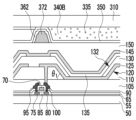
도 1은 본 발명의 일 실시예에 따른 표시 장치를 나타내는 단면도이다. 도 2는 도 1의 실시예에서 녹색 화소 영역을 나타내는 단면도이다. 도 3은 도 1의 실시예에서 청색 화소 영역을 나타내는 단면도이다. 도 4는 도 1의 표시 장치의 발광 소자를 나타내는 단면도이다.FIG. 1 is a cross-sectional view showing a display device according to one embodiment of the present invention. FIG. 2 is a cross-sectional view showing a green pixel area in the embodiment of FIG. 1. FIG. 3 is a cross-sectional view showing a blue pixel area in the embodiment of FIG. 1. FIG. 4 is a cross-sectional view showing a light-emitting element of the display device of FIG. 1.
도 1을 참고하면, 제1 기판(50) 위에 버퍼층(55)이 위치한다. 제1 기판(50)은 투명할 수 있다. Referring to Fig. 1, a buffer layer (55) is positioned on a first substrate (50). The first substrate (50) may be transparent.
버퍼층(55)은 제1 기판(50)으로부터 금속 원자들, 불순물들 등이 확산되는 현상을 방지하는 기능을 수행할 수 있다. 예를 들면, 버퍼층(55)은 실리콘 산화물, 실리콘 질화물, 실리콘 산질화물, 실리콘 산탄화물, 실리콘 탄질화물 등을 포함할 수 있다. 버퍼층(55)은 생략할 수 있다.The buffer layer (55) can perform a function of preventing metal atoms, impurities, etc. from diffusing from the first substrate (50). For example, the buffer layer (55) can include silicon oxide, silicon nitride, silicon oxynitride, silicon oxycarbide, silicon carbon nitride, etc. The buffer layer (55) can be omitted.
버퍼층(55) 위에 반도체층이 위치한다. 반도체층은 n형 또는 p형의 도전성 불순물을 포함하는 복수의 불순물 영역(extrinsic region)과 도전성 불순물을 거의 포함하지 않은 적어도 하나의 진성 영역(intrinsic region)을 포함할 수 있다.A semiconductor layer is positioned on the buffer layer (55). The semiconductor layer may include a plurality of extrinsic regions containing n-type or p-type conductive impurities and at least one intrinsic region containing almost no conductive impurities.
반도체층에서, 불순물 영역은 소스 및 드레인 영역(75, 80)을 포함하며, 이들은 p형 불순물로 도핑되어 있고 서로 분리되어 있다. 소스 영역(75)과 드레인 영역(80) 사이가 채널 영역(85)이 된다. 이와는 달리, 반도체층의 불순물 영역(75, 80)이 n형 불순물로 도핑될 수 있다.In the semiconductor layer, the impurity region includes source and drain regions (75, 80), which are doped with p-type impurities and separated from each other. The region between the source region (75) and the drain region (80) becomes a channel region (85). Alternatively, the impurity region (75, 80) of the semiconductor layer may be doped with n-type impurities.
반도체층 및 버퍼층(55) 위에는 산화 규소 또는 질화 규소로 이루어진 게이트 절연막(65)이 위치한다.A gate insulating film (65) made of silicon oxide or silicon nitride is positioned on the semiconductor layer and buffer layer (55).
게이트 절연막(65) 위에 게이트 전극(70)이 위치한다. 게이트 전극(70)은 게이트 절연막(65) 중에서 아래에 반도체층이 위치하는 게이트 절연막(65) 부분 위에 위치한다.A gate electrode (70) is positioned on the gate insulating film (65). The gate electrode (70) is positioned on the portion of the gate insulating film (65) where the semiconductor layer is positioned underneath.
도시하지 않았으나, 게이트 절연막(65) 위에 게이트 전극(70)과 연결되는 게이트선이 위치한다.Although not shown, a gate line connected to the gate electrode (70) is located on the gate insulating film (65).
게이트 절연막(65) 위에 게이트 전극(70)을 덮는 층간 절연막(90)이 위치할 수 있다. 층간 절연막(90)은 게이트 전극(70)의 프로파일을 따라 게이트 절연막(65) 위에 균일한 두께로 형성될 수 있다. 따라서, 층간 절연막(90)에는 게이트 전극(70)에 인접하는 단차부가 생성될 수 있다. 층간 절연막(90)은 실리콘 산화물, 실리콘 질화물, 실리콘 산질화물 등을 포함하는 실리콘 화합물을 사용하여 형성될 수 있다. 층간 절연막(90)은 후술하는 소스 전극(95)과 드레인 전극(100)으로부터 게이트 전극(70)을 절연시키는 역할을 수행할 수 있다.An interlayer insulating film (90) covering a gate electrode (70) may be positioned on the gate insulating film (65). The interlayer insulating film (90) may be formed with a uniform thickness on the gate insulating film (65) along the profile of the gate electrode (70). Accordingly, a step portion adjacent to the gate electrode (70) may be created in the interlayer insulating film (90). The interlayer insulating film (90) may be formed using a silicon compound including silicon oxide, silicon nitride, silicon oxynitride, or the like. The interlayer insulating film (90) may serve to insulate the gate electrode (70) from the source electrode (95) and the drain electrode (100) described below.
층간 절연막(90) 위에 소스 전극(95)과 드레인 전극(100)이 위치한다. 소스 전극 및 드레인 전극(95, 100)은 게이트 전극(70)을 중심으로 소정의 간격으로 이격되며, 게이트 전극(70)에 인접하여 위치한다. 예를 들면, 소스 및 드레인 전극(95, 100)은 각기 소스 및 드레인 영역(75, 80) 상부에 위치하는 층간 절연막(90)으로부터 게이트 전극(70) 위에 위치하는 층간 절연막(90)까지 연장될 수 있다. 또한, 소스 및 드레인 전극(95, 100)은 층간 절연막(90)을 관통하여 소스 및 드레인 영역(75, 80)에 각각 접촉된다.A source electrode (95) and a drain electrode (100) are positioned on an interlayer insulating film (90). The source electrode and the drain electrode (95, 100) are spaced apart from each other by a predetermined interval with respect to the gate electrode (70) and are positioned adjacent to the gate electrode (70). For example, the source and drain electrodes (95, 100) may extend from the interlayer insulating film (90) positioned above the source and drain regions (75, 80), respectively, to the interlayer insulating film (90) positioned above the gate electrode (70). In addition, the source and drain electrodes (95, 100) penetrate the interlayer insulating film (90) and contact the source and drain regions (75, 80), respectively.
소스 및 드레인 전극(95, 100)은 각각 금속, 합금, 금속 질화물, 도전성 금속 산화물, 투명 도전성 물질 등을 포함할 수 있다.The source and drain electrodes (95, 100) may each include a metal, an alloy, a metal nitride, a conductive metal oxide, a transparent conductive material, etc.
도시하지 않았으나, 층간 절연막(90) 위에 상기 게이트선과 교차하도록 데이터선이 소스 전극(95)과 연결되도록 위치한다.Although not shown, the data line is positioned to be connected to the source electrode (95) so as to intersect the gate line on the interlayer insulating film (90).
소스 전극(95) 및 드레인 전극(100) 위에 평탄화층(105)이 위치한다. 평탄화층(105)은 소스 전극(95) 및 드레인 전극(100)을 완전히 덮도록 충분한 두께를 가질 수 있다. 평탄화층(105)은 유기 물질, 물기 물질 등을 포함할 수 있다.A planarization layer (105) is positioned on the source electrode (95) and the drain electrode (100). The planarization layer (105) may have a sufficient thickness to completely cover the source electrode (95) and the drain electrode (100). The planarization layer (105) may include an organic material, a water-based material, or the like.
평탄화층(105) 위에 경사부(120)를 갖는 절연층(110)이 위치한다. 절연층(110)에는 평탄화층(105)과 함께 관통되어 드레인 전극(100)을 부분적으로 노출하는 접촉 구멍이 형성되어 있다. 이러한 접촉 구멍을 통해 드레인 전극(100)과 후술하는 제1 전극(125)이 전기적으로 연결될 수 있다.An insulating layer (110) having a sloped portion (120) is positioned on the flattening layer (105). A contact hole is formed in the insulating layer (110) that penetrates together with the flattening layer (105) and partially exposes the drain electrode (100). Through this contact hole, the drain electrode (100) and the first electrode (125) described below can be electrically connected.
본 실시예에 따른 절연층(110)은 일부 함몰된 부분을 가진다. 일부 함몰된 부분은 도 2에 도시한 바와 같이 평탄화층(105)의 상부면 일부를 드러낼 수 있다. 절연층(110)의 일부 함몰된 부분과 절연층(110)의 함몰되지 않은 다른 부분을 연결하는 측면은 경사부(120)를 형성할 수 있다. 본 실시예에서 경사부(120)는 제1 경사각(θ1)을 가지고, 제1 경사각(θ1)은 0 도 보다 크고 90 도 보다 작은 각도를 가질 수 있다. 도 1에서 나타낸 3개의 발광 영역(DA) 각각의 제1 경사각(θ1)이 모두 동일한 것으로 도시하였으나 시야각에 따른 색변화 개선을 위한 목적으로 각 발광 영역 별로 경사각이 서로 다르게 설계할 수도 있다.The insulating layer (110) according to the present embodiment has a partially sunken portion. The partially sunken portion may expose a portion of the upper surface of the flattening layer (105), as illustrated in FIG. 2. A side connecting the partially sunken portion of the insulating layer (110) and the other non-sunken portion of the insulating layer (110) may form an inclined portion (120). In the present embodiment, the inclined portion (120) has a first inclined angle (θ 1 ), and the first inclined angle (θ 1 ) may be greater than 0 degrees and less than 90 degrees. Although the first inclined angles (θ 1 ) of each of the three light-emitting areas (DA) illustrated in FIG. 1 are all illustrated as being the same, the inclined angles may be designed differently for each light-emitting area for the purpose of improving color change according to the viewing angle.
절연층(110) 위에 제1 전극(125)이 위치한다. 제1 전극(125)은 전술한 접촉 구멍에 채워져 드레인 전극(100)과 연결된다. 본 실시예에서 제1 전극(125)은 절연층(110)의 일부 함몰된 부분을 덮고, 경사부(120)를 따라 위치하는 기울어진 부분을 포함한다. 제1 전극(125)의 기울어진 부분은 제1 기판(50)에 실질적으로 평행한 면을 기준으로 기울어질 수 있다. 이 때, 제1 전극(125)의 경사 부분은 절연층(110)의 경사부(120) 대부분을 덮을 수 있다. 또한, 도 2에 도시한 것처럼 절연층(110)의 일부 함몰된 부분에서 제1 전극(125)은 평탄화층(105)의 상부면과 접촉할 수 있다.A first electrode (125) is positioned on the insulating layer (110). The first electrode (125) fills the aforementioned contact hole and is connected to the drain electrode (100). In the present embodiment, the first electrode (125) covers a partially sunken portion of the insulating layer (110) and includes an inclined portion positioned along the inclined portion (120). The inclined portion of the first electrode (125) may be inclined with respect to a plane substantially parallel to the first substrate (50). At this time, the inclined portion of the first electrode (125) may cover most of the inclined portion (120) of the insulating layer (110). In addition, as illustrated in FIG. 2, the first electrode (125) may contact the upper surface of the planarization layer (105) in the partially sunken portion of the insulating layer (110).
본 실시예와 같이 경사부(120)를 갖는 절연층(110)을 포함하는 표시 장치는, 제1 기판(50)으로부터 절연층(110)을 향하는 방향으로 최종적으로 광이 발광하는 전면 발광 방식을 가질 수 있다. 이 때, 제1 전극(125)은 반사 전극일 수 있다. A display device including an insulating layer (110) having an inclined portion (120) as in the present embodiment may have a front-emitting method in which light is ultimately emitted in a direction from the first substrate (50) toward the insulating layer (110). In this case, the first electrode (125) may be a reflective electrode.
본 개시에서 반사 전극이라고 함은 발광층(135)에서 발생한 광을 제2 전극(145)으로 보내기 위해 광을 반사하는 성질을 갖는 물질을 포함하는 전극으로 정의할 수 있다. 여기서, 반사하는 성질이란 입사광에 대한 반사율이 약 70% 이상 약 100% 이하이거나 약 80% 이상 약 100% 이하를 의미할 수 있다.In the present disclosure, a reflective electrode may be defined as an electrode including a material having a property of reflecting light in order to send light generated from a light-emitting layer (135) to a second electrode (145). Here, the reflective property may mean a reflectivity for incident light of about 70% or more and about 100% or less, or about 80% or more and about 100% or less.
제1 전극(125)은 은(Ag), 알루미늄(Al), 크롬(Cr), 몰리브덴(Mo), 텅스텐(W), 티타늄(Ti), 금(Au), 팔라듐(Pd) 또는 이들의 합금을 포함할 수 있고, 은(Ag)/산화인듐주석(ITO)/은(Ag)의 삼중막 구조 또는 산화인듐주석(ITO)/은(Ag)/산화인듐주석(ITO)의 삼중막 구조 등을 가질 수 있다.The first electrode (125) may include silver (Ag), aluminum (Al), chromium (Cr), molybdenum (Mo), tungsten (W), titanium (Ti), gold (Au), palladium (Pd), or an alloy thereof, and may have a triple film structure of silver (Ag)/indium tin oxide (ITO)/silver (Ag), or a triple film structure of indium tin oxide (ITO)/silver (Ag)/indium tin oxide (ITO).
제1 전극(125)은 스퍼터링(sputtering)법, 기상 증착(vapor phase deposition)법, 이온 빔 증착(ion beam deposition)법, 또는 전자빔 증착(electron beam deposition)법 등을 이용해서 형성할 수 있다. The first electrode (125) can be formed using a sputtering method, a vapor phase deposition method, an ion beam deposition method, or an electron beam deposition method.
절연층(110)과 제1 전극(125) 위에 화소 정의막(130)이 위치한다. 화소 정의막(130)은 유기 물질, 무기 물질 등을 사용하여 형성될 수 있다. 예를 들면, 화소 정의막(130)은 포토레지스트, 폴리아크릴계 수지, 폴리이미드계 수지, 아크릴계 수지 등의 유기 물질이나 실리콘 화합물과 같은 무기 물질을 포함할 수 있다. 화소 정의막(130)은 검정색 안료를 포함하는 감광제로 만드는 실시예도 가능하고, 이러한 경우에 화소 정의막(130)은 차광 부재의 역할을 할 수 있다.A pixel defining film (130) is positioned on the insulating layer (110) and the first electrode (125). The pixel defining film (130) may be formed using an organic material, an inorganic material, etc. For example, the pixel defining film (130) may include an organic material such as a photoresist, a polyacrylic resin, a polyimide resin, an acrylic resin, etc., or an inorganic material such as a silicon compound. The pixel defining film (130) may also be formed using a photosensitive agent including a black pigment, and in this case, the pixel defining film (130) may function as a light-blocking member.
화소 정의막(130)은 나노 구조의 산란 입자들이 분산되어 있을 수 있다. 산란 입자들은 무기 입자 또는 고분자 입자를 포함할 수 있다. 예를 들어, 실리카(silica), TiO2, ZrO2 등의 무기 입자 또는 폴리 스티렌, 폴리메틸메타아크릴레이트(PMMA) 등의 고분자 입자를 포함할 수 있다.The pixel definition film (130) may have nano-structured scattering particles dispersed therein. The scattering particles may include inorganic particles or polymer particles. For example, the scattering particles may include inorganic particles such as silica, TiO 2 , ZrO 2 , or polymer particles such as polystyrene, polymethyl methacrylate (PMMA).
화소 정의막(130)에는 제1 전극(125)의 일부를 노출하는 개구부(132)가 형성되어 있다. 개구부(132)에 의해 형성되는 화소 정의막(130)의 측면은 경사 구조를 가질 수 있고, 이러한 경사 구조의 경사각은 절연층(110)의 제1 경사각(θ1)과 실질적으로 동일하거나 유사할 수 있다. 실질적으로 동일하거나 유사한 범위는 대략 그 차이가 0 보다 크고 5도 이하일 수 있다. 이와 같은 실시예와 달리, 화소 정의막(130)이 갖는 경사 구조의 경사각은 절연층(110)의 제1 경사각(θ1)과 관계 없이 제1 경사각(θ1)과 다르게 형성할 수도 있다.An opening (132) that exposes a part of the first electrode (125) is formed in the pixel defining film (130). The side surface of the pixel defining film (130) formed by the opening (132) may have a sloped structure, and the slope angle of this sloped structure may be substantially the same as or similar to the first slope angle (θ 1 ) of the insulating layer (110). The substantially same or similar range may be approximately a difference greater than 0 and less than or equal to 5 degrees. Unlike this embodiment, the slope angle of the slope structure of the pixel defining film (130) may be formed differently from the first slope angle (θ 1 ) regardless of the first slope angle (θ 1 ) of the insulating layer (110).
화소 정의막(130)은 표시 장치의 발광 영역(DA)과 비발광 영역(PA)을 정의할 수 있다. 화소 정의막(130)의 개구부(132)가 위치하는 영역이 발광 영역(DA)에 대응하고, 개구부(132) 이외의 화소 정의막(130)이 위치하는 영역이 비발광 영역(PA)에 대응한다. 발광 영역(DA)은 후술하는 발광층(135)에서 빛이 나오는 부분에 대응할 수 있고, 비발광 영역(PA)은 발광 영역(DA)을 제외한 나머지 영역에 대응할 수 있다.The pixel defining film (130) can define an emission area (DA) and a non-emission area (PA) of the display device. The area where the opening (132) of the pixel defining film (130) is positioned corresponds to the emission area (DA), and the area where the pixel defining film (130) is positioned other than the opening (132) corresponds to the non-emission area (PA). The emission area (DA) can correspond to a portion where light is emitted from the emission layer (135) described below, and the non-emission area (PA) can correspond to the remaining area excluding the emission area (DA).
절연층(110)의 경사부(120) 대부분은 발광 영역(DA)에 위치하고, 발광 영역(DA)에서 제1 전극(125)은 경사부(120)의 측면을 덮도록 위치한다. 이 때, 발광 영역(DA)에서 화소 정의막(130)은 경사부(120)의 측면을 덮고 있는 제1 전극(125) 부분을 덮는다.Most of the inclined portion (120) of the insulating layer (110) is located in the light-emitting area (DA), and the first electrode (125) in the light-emitting area (DA) is positioned to cover the side surface of the inclined portion (120). At this time, in the light-emitting area (DA), the pixel defining film (130) covers the portion of the first electrode (125) that covers the side surface of the inclined portion (120).
발광 영역(DA)에 위치하는 제1 전극(125) 위에 발광층(135)이 위치하고, 발광층(135) 위에 제2 전극(145)이 위치한다. 제1 전극(125), 발광층(135) 및 제2 전극(145)은 발광 소자를 구성할 수 있다.A light-emitting layer (135) is positioned on a first electrode (125) located in a light-emitting area (DA), and a second electrode (145) is positioned on the light-emitting layer (135). The first electrode (125), the light-emitting layer (135), and the second electrode (145) can form a light-emitting element.
도 1에 도시한 실시예에서 발광층(135)은 화소 정의막(130)의 경사 구조의 측면을 따라 연장되어 화소 정의막(130)의 상부면 일부에도 위치할 수 있다. 하지만, 변형된 실시예에서, 발광층(135)은 실질적으로 개구부(132)에 의해 노출되는 제1 전극(125) 부분 또는 개구부(132)에 의해 노출되는 제1 전극(125) 부분과 이로부터 연장되어 화소 정의막(130)의 경사진 측면에만 위치할 수 있다.In the embodiment illustrated in FIG. 1, the light-emitting layer (135) may extend along the side surface of the inclined structure of the pixel defining film (130) and may also be positioned on a portion of the upper surface of the pixel defining film (130). However, in a modified embodiment, the light-emitting layer (135) may be positioned only on a portion of the first electrode (125) substantially exposed by the opening (132) or on a portion of the first electrode (125) exposed by the opening (132) and extended therefrom on the inclined side surface of the pixel defining film (130).
도 1에 도시하지 않았으나, 제1 전극(125)과 발광층(135) 사이에는 정공 주입층, 정공 수송층 등의 부대층을 포함하고, 제2 전극(145)과 발광층(135) 사이에는 전자 수송층, 전자 주입층 등의 부대층을 포함할 수 있다. 본 실시예에 따른 발광층(135)은 반도체 나노 입자들을 포함한다. 본 실시예에 따른 반도체 나노 입자는 청색을 발광하는 양자점을 포함할 수 있다. 이하에서는 반도체 나노 입자를 포함하는 발광층(135)을 포함하는 발광 소자에 대해 도 4를 참고하여 설명하기로 한다.Although not shown in FIG. 1, a hole injection layer, a hole transport layer, and the like may be included between the first electrode (125) and the light-emitting layer (135), and an electron transport layer, an electron injection layer, and the like may be included between the second electrode (145) and the light-emitting layer (135). The light-emitting layer (135) according to the present embodiment includes semiconductor nanoparticles. The semiconductor nanoparticles according to the present embodiment may include quantum dots that emit blue light. Hereinafter, a light-emitting element including a light-emitting layer (135) including semiconductor nanoparticles will be described with reference to FIG. 4.
도 4를 참고하면, 본 실시예에 따른 발광 소자는, 제1 전극(125) 위에 정공 수송 영역(1351), 정공 수송 영역(1351) 위에 위치하는 발광층(135), 발광층(135) 위에 위치하는 전자 수송 영역(1355) 및 전자 수송 영역(1355) 위에 위치하는 제2 전극(145)을 포함한다.Referring to FIG. 4, a light-emitting element according to the present embodiment includes a hole transport region (1351) on a first electrode (125), a light-emitting layer (135) positioned on the hole transport region (1351), an electron transport region (1355) positioned on the light-emitting layer (135), and a second electrode (145) positioned on the electron transport region (1355).
정공 수송 영역(1351)은 제1 전극(125)과 발광층(135) 사이에 위치하는 부대층을 포함할 수 있다. 정공 수송 영역(1351)은 정공 수송층과 정공 주입층 중 적어도 하나를 포함할 수 있다. 정공 수송층은 제1 전극(125)으로부터 전달되는 정공을 원활하게 수송하는 기능을 수행할 수 있다. 정공 수송층은 유기 물질을 포함할 수 있다. 예를 들면, 정공 수송층은 NPD(N,N-dinaphthyl-N,N'-diphenyl benzidine), TPD(N,N'-bis-(3-methylphenyl)-N,N'-bis-(phenyl)-benzidine), s-TAD, MTDATA(4,4',4"-Tris(N-3-methylphenyl-N-phenyl-amino)-triphenylamine) 등을 포함할 수 있으나, 이에 한정되는 것은 아니다.The hole transport region (1351) may include a sublayer positioned between the first electrode (125) and the light-emitting layer (135). The hole transport region (1351) may include at least one of a hole transport layer and a hole injection layer. The hole transport layer may perform a function of smoothly transporting holes transferred from the first electrode (125). The hole transport layer may include an organic material. For example, the hole transport layer may include, but is not limited to, NPD (N,N-dinaphthyl-N,N'-diphenyl benzidine), TPD (N,N'-bis-(3-methylphenyl)-N,N'-bis-(phenyl)-benzidine), s-TAD, MTDATA (4,4',4"-Tris(N-3-methylphenyl-N-phenyl-amino)-triphenylamine).
발광층(135)은 복수의 양자점을 포함하고, 발광층(135)을 이루는 물질은 특별히 제한되지 않는다. 또한 본 발명의 실시예에 따른 발광층(135)에 포함되는 양자점은 하나의 반도체 물질이 다른 반도체 물질을 둘러싸는 코어/쉘 구조를 가질 수 있다. 코어와 쉘의 계면은 쉘에 존재하는 원소의 농도가 중심으로 갈수록 낮아지는 농도 구배(gradient)를 가질 수 있다.The light-emitting layer (135) includes a plurality of quantum dots, and the material forming the light-emitting layer (135) is not particularly limited. In addition, the quantum dots included in the light-emitting layer (135) according to the embodiment of the present invention may have a core/shell structure in which one semiconductor material surrounds another semiconductor material. The interface between the core and the shell may have a concentration gradient in which the concentration of elements present in the shell decreases toward the center.
코어 및 쉘 각각은 Mg, Zn, Te, Se 및 S 중 적어도 2 종을 포함할 수 있으며, 특히 쉘이 포함하는 Mg의 함량은 상기 코어가 포함하는 Mg의 함량보다 클 수 있다. Each of the core and the shell may include at least two kinds of Mg, Zn, Te, Se and S, and in particular, the content of Mg included in the shell may be greater than the content of Mg included in the core.
구체적으로, Mg의 함량이 클수록 반도체가 가지는 밴드갭 에너지가 커지는데, 쉘이 포함하는 Mg의 함량이 코어가 포함하는 Mg의 함량보다 큰 경우, 쉘의 밴드갭 에너지가 코어의 밴드갭 에너지를 감싸는 형태로 제공될 수 있고, 이에 따르면 보다 안정적인 정공/전자 주입이 가능하다. Specifically, the larger the content of Mg, the larger the band gap energy of the semiconductor. When the content of Mg contained in the shell is larger than the content of Mg contained in the core, the band gap energy of the shell can be provided in a form that surrounds the band gap energy of the core, thereby enabling more stable hole/electron injection.
다시 말해, 쉘이 코어보다 더 많은 함량의 Mg를 포함하는 경우, 쉘은 코어의 HOMO 에너지 준위보다 낮은 HOMO 에너지 준위를 가지면서 코어의 LUMO 에너지 준위보다 높은 LUMO 에너지 준위를 가질 수 있다. 이러한 코어/쉘 에너지 준위 관계에 따르면 효율적인 정공 및 전자의 주입이 가능하여, 발광 소자의 발광 효율이 증대된다. In other words, when the shell contains a higher content of Mg than the core, the shell can have a HOMO energy level lower than the HOMO energy level of the core and a LUMO energy level higher than the LUMO energy level of the core. According to this core/shell energy level relationship, efficient hole and electron injection is possible, thereby increasing the luminescence efficiency of the light-emitting device.
코어는 Zn1-xMgxSe, Zn1-xMgxS, 및 Zn1-xMgxTe 중 적어도 하나를 포함할 수 있으며 상기 x는 0 이상 1 이하의 값이고, 쉘은 Zn1-yMgyTe, Zn1-yMgySe 및 Zn1-yMgyS 중 적어도 하나를 포함할 수 있으며 상기 y는 0 이상 1 이하의 값일 수 있다. 이때 쉘이 포함하는 Mg의 함량은 코어가 포함하는 Mg의 함량보다 크도록 코어는 Mg을 포함하지 않을 수 있으며 일례로 코어가 ZnTe 재질이고, 쉘이 MgTe일 수 있다. The core may include at least one of Zn 1-x Mg x Se, Zn 1-x Mg x S, and Zn 1-x Mg x Te, where x is a value greater than or equal to 0 and less than or equal to 1, and the shell may include at least one of Zn 1-y Mg y Te, Zn 1-y Mg y Se, and Zn 1-y Mg y S, where y is a value greater than or equal to 0 and less than or equal to 1. At this time, the core may not include Mg so that the content of Mg included in the shell is greater than the content of Mg included in the core. For example, the core may be made of a ZnTe material and the shell may be MgTe.
또한 코어가 Zn1-xMgxSe, Zn1-xMgxS, 및 Zn1-xMgxTe 중 적어도 하나를 포함하고, 쉘이 Zn1-yMgyTe, Zn1-yMgySe 및 Zn1-yMgyS 중 적어도 하나를 포함하는 경우, 쉘과 코어는 유사한 결정 구조를 가지며 이를 나타내는 격자 상수 값이 유사하다. 유사한 격자 상수 값은 코어/쉘 사이의 정합성이 우수함을 나타낸다. Additionally, when the core includes at least one of Zn 1-x Mg x Se, Zn 1-x Mg x S, and Zn 1-x Mg x Te, and the shell includes at least one of Zn 1 - y Mg y Te, Zn 1-y Mg y Se, and Zn 1-y Mg y S, the shell and the core have similar crystal structures and have similar lattice constant values representing this. Similar lattice constant values indicate excellent coherence between the core/shell.
구체적으로 섬아연석형구조(zinc blende structure)를 가지는 경우, ZnTe의 결정 상수는 6.103이고 MgTe의 결정 상수는 6.280이고 CdTe는 6.478의 결정 상수 값을 가진다. 이때 본 발명의 일 실시예에 따른 ZnTe(코어)와 MgTe(쉘)의 결정 상수의 차이값은 ZnTe(코어)와 CdTe(쉘)의 결정 상수의 차이값 보다 작은 값을 가질 수 있으며, 이는 본 발명에 따른 양자점이 기존 대비 결정 정합성이 우수할 수 있음을 나타낸다. Specifically, in the case of having a zinc blende structure, the crystal constant of ZnTe is 6.103, the crystal constant of MgTe is 6.280, and CdTe has a crystal constant value of 6.478. At this time, the difference value of the crystal constants of ZnTe (core) and MgTe (shell) according to an embodiment of the present invention may have a value smaller than the difference value of the crystal constants of ZnTe (core) and CdTe (shell), which indicates that the quantum dot according to the present invention may have superior crystal consistency compared to the existing one.
코어/쉘 양자점 중 코어의 평균 입경은 약 2nm 내지 약 5nm일 수 있다. 한편, 쉘의 평균 두께는 약 3nm 내지 약 5nm일 수 있다. 또한, 양자점의 평균 입경은 약 2nm 내지 약 10nm일 수 있다. Among the core/shell quantum dots, the average particle diameter of the core may be from about 2 nm to about 5 nm. Meanwhile, the average thickness of the shell may be from about 3 nm to about 5 nm. Additionally, the average particle diameter of the quantum dots may be from about 2 nm to about 10 nm.
상술한 바와 같은 범위 내에서 코어의 입경, 쉘의 평균 두께, 양자점의 평균 입경을 다양하게 선택함으로써, 양자점의 발광 컬러 및/또는 양자점의 반도체성 특성 등을 다양하게 변화시킬 수 있다.By variously selecting the core particle size, the average thickness of the shell, and the average particle size of the quantum dots within the ranges described above, the emission color of the quantum dots and/or the semiconductor properties of the quantum dots can be variously changed.
본 실시예에서 발광층(135)은 청색 발광할 수 있다.In this embodiment, the light-emitting layer (135) can emit blue light.
발광층(135) 위에 전자 수송 영역(1355)이 위치할 수 있다. 전자 수송 영역(1355)은 발광층(135)과 제2 전극(145) 사이에 위치하는 부대층을 포함할 수 있다. 전자 수송 영역(1355)은 전자 수송층과 전자 주입층 중 적어도 하나를 포함할 수 있다. 이때, 전자 수송층은 유기 물질을 포함할 수 있다. 예를 들어, 전자 수송층은 Alq3(tris(8-hydroxyquinolino)aluminum), PBD(2-[4-biphenyl-5-[4-tert-butylphenyl]]-1,3,4-oxadiazole), TAZ(1,2,4-triazole), spiro-PBD(spiro-2-[4-biphenyl-5-[4-tert-butylphenyl]]-1,3,4-oxadiazole), 및 BAlq(8-hydroxyquinoline beryllium salt)로 이루어진 군에서 선택된 어느 하나 이상으로 이루어질 수 있으나, 이에 한정되지 않는다.An electron transport region (1355) may be positioned on the light-emitting layer (135). The electron transport region (1355) may include a sublayer positioned between the light-emitting layer (135) and the second electrode (145). The electron transport region (1355) may include at least one of an electron transport layer and an electron injection layer. At this time, the electron transport layer may include an organic material. For example, the electron transport layer may be formed of one or more selected from the group consisting of Alq3 (tris(8-hydroxyquinolino)aluminum), PBD (2-[4-biphenyl-5-[4-tert-butylphenyl]]-1,3,4-oxadiazole), TAZ (1,2,4-triazole), spiro-PBD (spiro-2-[4-biphenyl-5-[4-tert-butylphenyl]]-1,3,4-oxadiazole), and BAlq (8-hydroxyquinoline beryllium salt), but is not limited thereto.
도 5는 도 4의 발광 소자를 변형한 텐덤 구조를 나타내는 단면도이다.Fig. 5 is a cross-sectional view showing a tandem structure that is a modified version of the light-emitting element of Fig. 4.
도 5를 참고하면, 본 개시의 일 실시예에 따른 발광 소자는 텐덤형 구조를 가질 수 있다. 예를 들어, 발광층(135)은 서로 동일한 색을 발광하거나 서로 다른 색을 발광하는 2개의 층(1352, 1353)을 포함할 수 있다. 서로 동일한 색을 발광하는 2개의 층(1352, 1353)은 모두 청색 발광층일 수 있다. 서로 다른 색을 발광하는 2개의 층(1352, 1353) 가운데 어느 하나는 청색 발광층이고, 다른 하나는 녹색 발광층 또는 노란색 발광층일 수 있다. 2개의 발광층 각각에서 발생한 광이 서로 혼합되어 청색 또는 백색을 나타낼 수 있다. 이에 한정되지 않고 발광층(135)은 서로 다른 색을 발광하는 3개의 층, 또는 2개 층은 동일하지만 1개 층은 다른 색을 발광하는 3개의 층을 포함할 수 있다. 이 때 3개의 층은 각각 적색, 녹색 및 청색을 발광하거나 청색, 노란색, 청색을 발광할 수 있고, 3개의 층 각각에서 발생한 광이 서로 혼합되어 청색 또는 백색을 나타낼 수 있다.Referring to FIG. 5, a light-emitting element according to an embodiment of the present disclosure may have a tandem structure. For example, the light-emitting layer (135) may include two layers (1352, 1353) that emit the same color or emit different colors. Both of the two layers (1352, 1353) that emit the same color may be blue light-emitting layers. One of the two layers (1352, 1353) that emit different colors may be a blue light-emitting layer, and the other may be a green light-emitting layer or a yellow light-emitting layer. Light generated from each of the two light-emitting layers may be mixed to exhibit blue or white. Without being limited thereto, the light-emitting layer (135) may include three layers that emit different colors, or three layers in which two layers are the same but one layer emits a different color. At this time, the three layers can emit red, green, and blue, or blue, yellow, and blue, respectively, and the light generated from each of the three layers can be mixed to produce blue or white.
도시하지 않았으나 2개의 층(1352, 1353) 사이에 전하 생성층이 위치할 수 있다. 전하 생성층은 통상적으로, 이웃하는 발광층 사이에 형성되어 인접하는 발광층 간의 전하 균형을 조절하는 역할을 한다.Although not shown, a charge generation layer may be located between the two layers (1352, 1353). The charge generation layer is typically formed between adjacent light-emitting layers and serves to control the charge balance between adjacent light-emitting layers.
도 1을 다시 참고하면, 발광층(135) 및 화소 정의막(130) 위에 제2 전극(145)이 위치한다. 제2 전극(145)은 반투과 전극일 수 있다.Referring again to Figure 1, a second electrode (145) is positioned on the light-emitting layer (135) and the pixel defining film (130). The second electrode (145) may be a semi-transparent electrode.
본 개시에서 반투과 전극이라고 함은 제2 전극(145)으로 입사한 광의 일부를 투과시키고, 나머지 광을 제1 전극(125)으로 반사하는 반투과 성질을 갖는 물질을 포함하는 전극으로 정의할 수 있다. 여기서, 반투과 성질이란 입사광에 대한 반사율이 약 0.1% 이상 약 70% 미만이거나 약 30% 이상 50% 이하를 의미할 수 있다.In the present disclosure, a semi-transparent electrode may be defined as an electrode including a material having a semi-transparent property that transmits a portion of light incident on the second electrode (145) and reflects the remaining light to the first electrode (125). Here, the semi-transparent property may mean a reflectivity for incident light of about 0.1% or more and less than about 70% or about 30% or more and less than about 50%.
제2 전극(145)은 은(Ag), 마그네슘(Mg), 알루미늄(Al), 크롬(Cr), 몰리브덴(Mo), 텅스텐(W), 티타늄(Ti), 금(Au), 팔라듐(Pd), 이터븀(Yb) 또는 이들의 합금을 포함할 수 있다. 이상에서, 제2 전극(145)의 한 예로 공진 구조를 설명하기 위해 반투과 전극인 것으로 설명하였으나, 본 개시의 다른 일 실시예에 따르면 비공진 구조도 적용 가능하고, 이때 제2 전극(145)은 ITO 또는 IZO와 같은 투명 전도성 전극일 수도 있다.The second electrode (145) may include silver (Ag), magnesium (Mg), aluminum (Al), chromium (Cr), molybdenum (Mo), tungsten (W), titanium (Ti), gold (Au), palladium (Pd), ytterbium (Yb), or an alloy thereof. In the above, the second electrode (145) was described as a semi-transparent electrode to explain the resonant structure as an example, but according to another embodiment of the present disclosure, a non-resonant structure may also be applied, and in this case, the second electrode (145) may be a transparent conductive electrode such as ITO or IZO.
도 1에 도시한 바와 같이, 제2 전극(145)은 발광 영역(DA)으로부터 비발광 영역(PA)까지 연장될 수 있다. 이에 한정되지 않고 제2 전극(145)은 발광 영역(DA) 또는 발광층(135)의 상부면에만 위치할 수도 있다. As illustrated in Fig. 1, the second electrode (145) may extend from the light-emitting area (DA) to the non-light-emitting area (PA). However, the second electrode (145) may not be limited thereto and may be positioned only on the upper surface of the light-emitting area (DA) or the light-emitting layer (135).
제2 전극(145) 위에 캡핑층(150)이 위치한다. 캡핑층(150)은 발광 영역(DA)으로부터 비발광 영역(PA)까지 연장될 수 있다. 캡핑층(150)은 유기 물질, 무기 물질 등을 사용하여 형성될 수 있다. 예를 들면, 캡핑층(150)은 포토 레지스트, 아크릴계 폴리머, 폴리이미드계 폴리머, 폴리아미드계 폴리머, 실록산계 폴리머, 감광성 아크릴 카르복실기를 포함하는 폴리머, 노볼락 수지, 알칼리 가용성 수지, 실리콘 산화물, 실리콘 질화물, 실리콘 산질화물, 실리콘 산탄화물, 실리콘 탄질화물, 알루미늄, 마그네슘, 아연, 하프늄, 지르코늄, 티타늄, 탄탈륨, 알루미늄 산화물, 티타늄 산화물, 탄탈륨 산화물, 마그네슘 산화물, 아연 산화물, 하프늄 산화물, 지르코늄 산화물, 티타늄 산화물 등을 포함할 수 있다. 이들은 단독으로 또는 서로 조합되어 사용될 수 있다.A capping layer (150) is positioned on the second electrode (145). The capping layer (150) can extend from the light-emitting area (DA) to the non-light-emitting area (PA). The capping layer (150) can be formed using an organic material, an inorganic material, or the like. For example, the capping layer (150) can include a photoresist, an acrylic polymer, a polyimide polymer, a polyamide polymer, a siloxane polymer, a polymer including a photosensitive acrylic carboxyl group, a novolak resin, an alkali-soluble resin, silicon oxide, silicon nitride, silicon oxynitride, silicon oxycarbide, silicon carbonitride, aluminum, magnesium, zinc, hafnium, zirconium, titanium, tantalum, aluminum oxide, titanium oxide, tantalum oxide, magnesium oxide, zinc oxide, hafnium oxide, zirconium oxide, titanium oxide, or the like. These can be used alone or in combination with each other.
캡핑층(150) 위에 제1 색변환층(340R), 제2 색변환층(340G) 및 투과층(340B)이 위치한다. 서로 이웃하는 제1 색변환층(340R)과 제2 색변환층(340G) 사이, 제1 색변환층(340R)과 투과층(340B) 사이, 제2 색변환층(340G)과 투과층(340B) 사이에 차광 부재(372)가 위치한다. 차광 부재(372)는 서로 인접한 색변환층(340R, 340G) 사이 및 서로 인접한 색변환층(340R, 340G)과 투과층(340B) 사이에서 발생하는 혼색을 보다 효과적으로 방지할 수 있다. A first color conversion layer (340R), a second color conversion layer (340G), and a transparent layer (340B) are positioned on the capping layer (150). A light-blocking member (372) is positioned between the adjacent first color conversion layers (340R) and the second color conversion layer (340G), between the first color conversion layer (340R) and the transparent layer (340B), and between the second color conversion layer (340G) and the transparent layer (340B). The light-blocking member (372) can more effectively prevent color mixing that occurs between adjacent color conversion layers (340R, 340G) and between adjacent color conversion layers (340R, 340G) and the transparent layer (340B).
이하에서는 도 2를 참고하여 제2 색변환층(340G)을 포함하는 녹색 화소 영역 및 녹색 화소 영역과 대체로 유사한 구성을 갖는 적색 화소 영역에 대해 설명하기로 한다.Hereinafter, with reference to FIG. 2, a green pixel area including a second color conversion layer (340G) and a red pixel area having a configuration generally similar to the green pixel area will be described.
도 1 및 도 2를 참고하면, 캡핑층(150)과 제2 색변환층(340G) 사이에 광필터층(350)이 위치할 수 있다. 광필터층(350)은 서로 이웃하는 색변환층(340R, 340G) 사이 및 서로 이웃하는 색변환층(340R, 340G)과 투과층(340B) 사이에도 위치하고, 이 때 제1 기판(50)에 실질적으로 수직한 방향을 기준으로 후술하는 제2 기판(310)과 차광 부재(372) 사이에 위치할 수 있다. 광필터층(350)은 제1, 2 색변환층(340R, 340G)에서 발생된 광을 반사시켜 광효율을 높이는 역할을 한다. 구체적으로, 광필터층(350)은, 발광층(135)에서 발생한 청색광이 색변환층(340R, 340G)의 반도체 나노 입자와 만나 적색 또는 녹색으로 램버시안(Lambertian) 산란하게 되고, 이때 정면이 아닌 측면 및 하부면으로 나가게 되는 적색광 또는 녹색광을 리사이클하고, 정면으로 나가게 하는 역할을 한다.Referring to FIGS. 1 and 2, a light filter layer (350) may be positioned between the capping layer (150) and the second color conversion layer (340G). The light filter layer (350) may be positioned between adjacent color conversion layers (340R, 340G) and between adjacent color conversion layers (340R, 340G) and the transparent layer (340B). In this case, the light filter layer (350) may be positioned between the second substrate (310) and the light blocking member (372) described below based on a direction substantially perpendicular to the first substrate (50). The light filter layer (350) serves to reflect light generated from the first and second color conversion layers (340R, 340G) to increase light efficiency. Specifically, the light filter layer (350) causes the blue light generated from the light-emitting layer (135) to meet the semiconductor nanoparticles of the color conversion layer (340R, 340G) and is scattered in a Lambertian manner into red or green, and recycles the red or green light that is emitted to the side and bottom instead of the front, and causes it to be emitted to the front.
광필터층(350)은 복수의 층을 포함하고, 복수의 층은 굴절률이 서로 다른 층들이 적어도 2 이상, 제1 기판(50)에 실질적으로 수직한 방향으로 교대 배열된 구조를 가질 수 있다.The optical filter layer (350) includes a plurality of layers, and the plurality of layers may have a structure in which at least two layers having different refractive indices are alternately arranged in a direction substantially perpendicular to the first substrate (50).
제2 색변환층(340G)과 차광 부재(372) 사이에 보조 금속층(362)이 위치한다. 보조 금속층(362)은 광 반사가 가능한 금속 물질일 수 있고, 보조 금속층(362)으로 입사하는 광을 다시 색변환층(340R, 340G), 투과층(340B) 또는 제2 기판(310)으로 반사시켜 사용자에게 방출되는 광량을 증가시킬 수 있다. 보조 금속층(362)은 생략될 수도 있다.An auxiliary metal layer (362) is positioned between the second color conversion layer (340G) and the light-shielding member (372). The auxiliary metal layer (362) may be a metal material capable of reflecting light, and may reflect light incident on the auxiliary metal layer (362) back to the color conversion layer (340R, 340G), the transmission layer (340B), or the second substrate (310) to increase the amount of light emitted to the user. The auxiliary metal layer (362) may be omitted.
제2 색변환층(340G) 위에 청색 차단 필터(322)가 위치한다. 청색 차단 필터(322)는 제1 색변환층(340R) 위에도 위치한다. 청색 차단 필터(322)는 다음과 같은 역할을 한다. 청색 발광 물질을 포함하는 발광층(135)을 사용한 경우에, 청색광이 제1 색변환층(340R) 및 제2 색변환층(340G)을 통과하여 각각 적색 및 녹색을 구현하는 과정에서 혼색이 발생하는 것을 방지한다. 구체적으로, 청색 차단 필터(322)는 제1 색변환층(340R) 및 제2 색변환층(340G)에서 흡수되지 않은 청색광을 외부로 나가지 못하게 차단하여, 제1 색변환층(340R)과 중첩하는 청색 차단 필터(322)는 청색광이 섞이지 않은 순수한 적색광을 투과시키고, 제2 색변환층(340G)과 중첩하는 청색 차단 필터(322)는 청색광이 섞이지 않은 순수한 녹색광을 투과시킬 수 있다.A blue blocking filter (322) is positioned on the second color conversion layer (340G). The blue blocking filter (322) is also positioned on the first color conversion layer (340R). The blue blocking filter (322) has the following role. When a light-emitting layer (135) including a blue light-emitting material is used, it prevents color mixing from occurring in the process of blue light passing through the first color conversion layer (340R) and the second color conversion layer (340G) to implement red and green, respectively. Specifically, the blue blocking filter (322) blocks blue light that is not absorbed by the first color conversion layer (340R) and the second color conversion layer (340G) from escaping to the outside, so that the blue blocking filter (322) overlapping the first color conversion layer (340R) can transmit pure red light that is not mixed with blue light, and the blue blocking filter (322) overlapping the second color conversion layer (340G) can transmit pure green light that is not mixed with blue light.
도 1, 2에서 청색 차단 필터(322)가 제1 색변환층(340R) 및 제2 색변환층(340G)과 대응하는 영역에 각각 위치하고, 각 영역에 위치하는 청색 차단 필터(322)가 서로 분리된 것으로 도시되어 있으나, 이와 달리 제1 색변환층(340R) 위에 형성된 청색 차단 필터(322)와 제2 색변환층(340G) 위에 형성된 청색 차단 필터(322)가 서로 연결될 수도 있다.In FIGS. 1 and 2, the blue blocking filter (322) is positioned in an area corresponding to the first color conversion layer (340R) and the second color conversion layer (340G), and the blue blocking filters (322) positioned in each area are shown as being separated from each other. However, unlike this, the blue blocking filter (322) formed on the first color conversion layer (340R) and the blue blocking filter (322) formed on the second color conversion layer (340G) may be connected to each other.
본 실시예에서 제1, 2 색변환층(340R, 340G) 및 투과층(340B)은 감광성 수지를 포함할 수 있다. 제1, 2 색변환층(340R, 340G)에 포함되는 양자점은 II-VI족 화합물, III-V족 화합물, IV-VI족 화합물, IV족 원소, IV족 화합물 및 이들의 조합에서 선택될 수 있다.In this embodiment, the first and second color conversion layers (340R, 340G) and the transparent layer (340B) may include a photosensitive resin. The quantum dots included in the first and second color conversion layers (340R, 340G) may be selected from a II-VI group compound, a III-V group compound, an IV-VI group compound, a IV group element, a IV group compound, and a combination thereof.
II-VI족 화합물은 CdSe, CdTe, ZnS, ZnSe, ZnTe, ZnO, HgS, HgSe, HgTe, MgSe, MgS 및 이들의 혼합물로 이루어진 군에서 선택되는 이원소 화합물; CdSeS, CdSeTe, CdSTe, ZnSeS, ZnSeTe, ZnSTe, HgSeS, HgSeTe, HgSTe, CdZnS, CdZnSe, CdZnTe, CdHgS, CdHgSe, CdHgTe, HgZnS, HgZnSe, HgZnTe, MgZnSe, MgZnS 및 이들의 혼합물로 이루어진 군에서 선택되는 삼원소 화합물; 및 HgZnTeS, CdZnSeS, CdZnSeTe, CdZnSTe, CdHgSeS, CdHgSeTe, CdHgSTe, HgZnSeS, HgZnSeTe, HgZnSTe 및 이들의 혼합물로 이루어진 군에서 선택되는 사원소 화합물로 이루어진 군에서 선택될 수 있다. III-V족 화합물은 GaN, GaP, GaAs, GaSb, AlN, AlP, AlAs, AlSb, InN, InP, InAs, InSb 및 이들의 혼합물로 이루어진 군에서 선택되는 이원소 화합물; GaNP, GaNAs, GaNSb, GaPAs, GaPSb, AlNP, AlNAs, AlNSb, AlPAs, AlPSb, InNP, InNAs, InNSb, InPAs, InPSb 및 이들의 혼합물로 이루어진 군에서 선택되는 삼원소 화합물; 및 GaAlNAs, GaAlNSb, GaAlPAs, GaAlPSb, GaInNP, GaInNAs, GaInNSb, GaInPAs, GaInPSb, GaAlNP, InAlNP, InAlNAs, InAlNSb, InAlPAs, InAlPSb 및 이들의 혼합물로 이루어진 군에서 선택되는 사원소 화합물로 이루어진 군에서 선택될 수 있다. IV-VI족 화합물은 SnS, SnSe, SnTe, PbS, PbSe, PbTe 및 이들의 혼합물로 이루어진 군에서 선택되는 이원소 화합물; SnSeS, SnSeTe, SnSTe, PbSeS, PbSeTe, PbSTe, SnPbS, SnPbSe, SnPbTe 및 이들의 혼합물로 이루어진 군에서 선택되는 삼원소 화합물; 및 SnPbSSe, SnPbSeTe, SnPbSTe 및 이들의 혼합물로 이루어진 군에서 선택되는 사원소 화합물로 이루어진 군에서 선택될 수 있다. IV족 원소로는 Si, Ge 및 이들의 혼합물로 이루어진 군에서 선택될 수 있다. IV족 화합물로는 SiC, SiGe 및 이들의 혼합물로 이루어진 군에서 선택되는 이원소 화합물일 수 있다. The group II-VI compound is a binary compound selected from the group consisting of CdSe, CdTe, ZnS, ZnSe, ZnTe, ZnO, HgS, HgSe, HgTe, MgSe, MgS and mixtures thereof; a ternary compound selected from the group consisting of CdSeS, CdSeTe, CdSTe, ZnSeS, ZnSeTe, ZnSTe, HgSeS, HgSeTe, HgSTe, CdZnS, CdZnSe, CdZnTe, CdHgS, CdHgSe, CdHgTe, HgZnS, HgZnSe, HgZnTe, MgZnSe, MgZnS and mixtures thereof; And the group consisting of quaternary compounds selected from the group consisting of HgZnTeS, CdZnSeS, CdZnSeTe, CdZnSTe, CdHgSeS, CdHgSeTe, CdHgSTe, HgZnSeS, HgZnSeTe, HgZnSTe and mixtures thereof. The group III-V compound may be selected from the group consisting of binary compounds selected from the group consisting of GaN, GaP, GaAs, GaSb, AlN, AlP, AlAs, AlSb, InN, InP, InAs, InSb and mixtures thereof; ternary compounds selected from the group consisting of GaNP, GaNAs, GaNSb, GaPAs, GaPSb, AlNP, AlNAs, AlNSb, AlPAs, AlPSb, InNP, InNAs, InNSb, InPAs, InPSb and mixtures thereof. And a group consisting of four-element compounds selected from the group consisting of GaAlNAs, GaAlNSb, GaAlPAs, GaAlPSb, GaInNP, GaInNAs, GaInNSb, GaInPAs, GaInPSb, GaAlNP, InAlNP, InAlNAs, InAlNSb, InAlPAs, InAlPSb and mixtures thereof. The Group IV-VI compound may be selected from the group consisting of a binary compound selected from the group consisting of SnS, SnSe, SnTe, PbS, PbSe, PbTe and mixtures thereof; a ternary compound selected from the group consisting of SnSeS, SnSeTe, SnSTe, PbSeS, PbSeTe, PbSTe, SnPbS, SnPbSe, SnPbTe and mixtures thereof; and a group consisting of four-element compounds selected from the group consisting of SnPbSSe, SnPbSeTe, SnPbSTe and mixtures thereof. The Group IV element may be selected from the group consisting of Si, Ge and mixtures thereof. The group IV compound may be a binary compound selected from the group consisting of SiC, SiGe, and mixtures thereof.
이때, 이원소 화합물, 삼원소 화합물 또는 사원소 화합물은 균일한 농도로 입자 내에 존재하거나, 농도 분포가 부분적으로 다른 상태로 나누어져 동일 입자 내에 존재하는 것일 수 있다. 또한 하나의 양자점이 다른 양자점을 둘러싸는 코어/쉘 구조를 가질 수도 있다. 코어와 쉘의 계면은 쉘에 존재하는 원소의 농도가 중심으로 갈수록 낮아지는 농도 구배(gradient)를 가질 수 있다.At this time, the binary, ternary or quaternary compound may exist in the particle at a uniform concentration, or may exist in the same particle with a partially different concentration distribution. In addition, one quantum dot may have a core/shell structure surrounding another quantum dot. The interface between the core and the shell may have a concentration gradient in which the concentration of the element existing in the shell decreases toward the center.
양자점은 약 45nm 이하, 바람직하게는 약 40nm 이하, 더욱 바람직하게는 약 30nm 이하의 발광 파장 스펙트럼의 반치폭(full width of half maximum, FWHM)을 가질 수 있으며, 이 범위에서 색순도나 색재현성을 향상시킬 수 있다. 또한 이러한 양자점을 통해 발광되는 광은 전 방향으로 방출되는바, 시야각이 넓어질 수 있다. Quantum dots can have a full width of half maximum (FWHM) of an emission wavelength spectrum of about 45 nm or less, preferably about 40 nm or less, and more preferably about 30 nm or less, and color purity or color reproducibility can be improved within this range. In addition, since light emitted through these quantum dots is emitted in all directions, the viewing angle can be widened.
또한, 양자점의 형태는 당 분야에서 일반적으로 사용하는 형태의 것으로 특별히 한정하지 않지만, 보다 구체적으로 구형, 피라미드형, 다중 가지형(multi-arm), 또는 입방체(cubic)의 나노 입자, 나노 튜브, 나노와이어, 나노 섬유, 나노 판상 입자 등의 형태의 것을 사용할 수 있다.In addition, the shape of the quantum dot is not particularly limited to a shape commonly used in the field, but more specifically, a shape such as a spherical, pyramidal, multi-arm, or cubic nanoparticle, nanotube, nanowire, nanofiber, or nanoplatelet particle can be used.
이하에서는 도 3을 참고하여 투과층(340B)을 포함하는 청색 화소 영역에 대해 설명하기로 한다.Below, the blue pixel area including the transparent layer (340B) will be described with reference to FIG. 3.
투과층(340B)은 투명 폴리머로 이루어져 있으며, 발광층(135)에서 공급된 청색광이 투과하며 청색을 나타낸다. 청색을 출광하는 영역에 해당하는 투과층(340B)은 별도의 형광체 또는 양자점 없이 입사된 청색을 출광하는 물질을 포함한다. 예를 들면, 투과층(340B)은 감광성 수지 등의 폴리머일 수 있다.The transmission layer (340B) is made of a transparent polymer, and the blue light supplied from the light-emitting layer (135) is transmitted through it and exhibits a blue color. The transmission layer (340B) corresponding to the area that emits blue light includes a material that emits incident blue light without a separate fluorescent substance or quantum dot. For example, the transmission layer (340B) may be a polymer such as a photosensitive resin.
본 실시예에서 투과층(340B)은 산란체(335)를 더 포함할 수 있다. 산란체(335)는 투과층(340B)으로부터 방출되는 광의 정면 휘도와 측면 휘도를 균일하게 할 수 있다. 산란체(335)는 광을 고르게 산란시키기 위한 어떠한 재질도 가능하며, 일례로써 실리카(silica; SiO2), 중공 실리카(속이 빈 구조의 SiO2), TiO2, ZrO2, Al2O3, In2O3, ZnO, SnO2, Sb2O3 및 ITO 중 어느 하나일 수 있다. 여기서, 중공 실리카의 속이 빈 구조에서 빈 공간은 가스로 채워지거나 진공일 수 있다.In the present embodiment, the transmitting layer (340B) may further include a scatterer (335). The scatterer (335) may make the front brightness and the side brightness of the light emitted from the transmitting layer (340B) uniform. The scatterer (335) may be any material that can evenly scatter the light, and as an example, may be any one of silica (SiO 2 ), hollow silica (SiO 2 having a hollow structure), TiO 2 , ZrO 2 , Al 2 O 3 , In 2 O 3 , ZnO, SnO 2 , Sb 2 O 3 , and ITO. Here, the empty space in the hollow structure of the hollow silica may be filled with gas or may be a vacuum.
산란체(335)의 크기는 하기 식 1의 범위를 가질 수 있다.The size of the scatterer (335) can have a range of the following equation 1.
λ/10 < PSQD < 5 λ 식 1λ/10 < PS QD < 5 λ Equation 1
식 1에서 λ는 형광체 또는 양자점의 발광 파장(나노미터)이고, PSQD는 형광체 또는 양자점의 응집 입도(나노미터)를 나타낸다.In Equation 1, λ is the emission wavelength (nanometers) of the fluorescent substance or quantum dot, and PS QD represents the aggregate particle size (nanometers) of the fluorescent substance or quantum dot.
도 1 및 도 3에 도시한 바와 같이 투과층(340B)에 산란체(335)가 포함되는 것을 설명하였으나, 변형된 일례로써 제1 색변환층(340R) 및 제2 색변환층(340G)에도 산란체가 포함될 수 있다.As illustrated in FIGS. 1 and 3, the scatterer (335) is included in the transmission layer (340B), but as a modified example, the scatterer may also be included in the first color conversion layer (340R) and the second color conversion layer (340G).
투과층(340B)은 청색 안료 또는 염료 중 어느 하나를 더 포함할 수 있다. 앞에서 설명한 산란체(335)가 외광을 반사시켜 명암비를 떨어뜨릴 수 있고, 이러한 문제를 보완하기 위해 청색 안료 또는 염료가 투과층(340B)에 첨가될 수 있다. 청색 안료 또는 염료는 외광에 포함된 적색 광과 녹색 광 중 적어도 하나를 흡수할 수 있다.The transmission layer (340B) may further include either a blue pigment or dye. The scattering material (335) described above may reflect external light, thereby reducing the contrast ratio, and to compensate for this problem, a blue pigment or dye may be added to the transmission layer (340B). The blue pigment or dye may absorb at least one of red light and green light included in the external light.
도 1 내지 도 3을 참고하면, 제1 색변환층(340R), 제2 색변환층(340G) 및 투과층(340B) 위에 제2 기판(310)이 위치한다. 도시하지 않았으나, 제2 기판(310) 위에 외광 반사를 방지하기 위한 λ/4 편광판을 더 포함할 수 있다.Referring to FIGS. 1 to 3, a second substrate (310) is positioned on the first color conversion layer (340R), the second color conversion layer (340G), and the transparent layer (340B). Although not shown, a λ/4 polarizing plate may be further included on the second substrate (310) to prevent external light reflection.
도 6은 도 1의 표시 장치의 발광층에서 발생한 광의 경로를 개략적으로 나타내는 단면도이다.Fig. 6 is a cross-sectional view schematically showing the path of light generated in the light-emitting layer of the display device of Fig. 1.
도 6을 참고하면, 제1 전극(125)이 갖는 경사 구조에 의해 광의 전반사를 방지하고 제1 전극(125)에 의해 광이 반사되어 제1, 2 색변환층(340R, 340G)을 포함하는 색변환층 및 투과층(340B)으로 전달될 수 있다.Referring to FIG. 6, the total reflection of light is prevented by the inclined structure of the first electrode (125), and the light can be reflected by the first electrode (125) and transmitted to the color conversion layer including the first and second color conversion layers (340R, 340G) and the transmission layer (340B).
따라서, 본 개시의 일 실시예에 따른 표시 장치에서는 발광층(135)에서 발생되는 광이 제1 전극(125) 및 제2 전극(145) 사이에서 전반사되어 광손실이 발생하는 것을 방지하고, 발광 소자 위에 위치하는 색변환층 및 투과층에 의해 출광 효율이 극대화될 수 있다. 본 실시예에 따른 색변환층은 형광체 및 양자점을 적어도 하나 포함하여 형성되기 때문에 종래의 표시 장치가 가지고 있던 색편이 현상을 최소화할 수 있다. 또, 발광층으로 반도체 나노 입자를 사용하기 때문에 발광층에서부터 램버시안 분포로 빛이 발광되고, 이에 따라 산란 효과가 매우 크게 되어 효율이 더욱 상승할 수 있다.Therefore, in the display device according to one embodiment of the present disclosure, the light generated from the light-emitting layer (135) is prevented from being totally reflected between the first electrode (125) and the second electrode (145), thereby causing light loss, and the light output efficiency can be maximized by the color conversion layer and the transparent layer positioned on the light-emitting element. Since the color conversion layer according to the present embodiment is formed by including at least one fluorescent substance and one quantum dot, the color shift phenomenon that the conventional display device has can be minimized. In addition, since semiconductor nanoparticles are used as the light-emitting layer, light is emitted from the light-emitting layer in a Lambertian distribution, and accordingly, the scattering effect is greatly increased, so that the efficiency can be further increased.
도 7은 도 1의 실시예에서 요철 구조를 포함하는 전극을 나타내는 단면도이다.FIG. 7 is a cross-sectional view showing an electrode including a rough structure in the embodiment of FIG. 1.
도 7을 참고하면, 경사부(120)에 인접한 평탄화층(105)의 상부면에 요철 구조(115)가 형성되어 있다. 이러한 요철 구조(115)로 인해 제1 전극(125) 표면이 복수의 돌기(116)를 가질 수 있다. 돌기(116)는 사각형뿐만 아니라 원형, 타원형, 마름모, 삼각형의 형상 등의 다양한 평면 형상을 가질 수 있다. 제1 전극(125)이 돌기(116)를 가지기 때문에 발광층(135)에서 발생되는 광이 반사되어 표시 장치의 광 효율을 더욱 향상시킬 수 있다.Referring to Fig. 7, a rough structure (115) is formed on the upper surface of the flattening layer (105) adjacent to the inclined portion (120). Due to this rough structure (115), the surface of the first electrode (125) can have a plurality of protrusions (116). The protrusions (116) can have various plane shapes such as not only a square shape but also a circle, an oval, a rhombus, a triangle, etc. Since the first electrode (125) has the protrusions (116), light generated from the light-emitting layer (135) is reflected, thereby further improving the light efficiency of the display device.
도 8은 도 1의 실시예에서 제2 전극 구조를 변형한 실시예를 나타내는 단면도이다.Fig. 8 is a cross-sectional view showing an embodiment in which the second electrode structure is modified from the embodiment of Fig. 1.
도 8을 참고하면, 도 1의 실시예와 대부분 동일하나, 발광층(135) 구조에 차이가 있다. 본 실시예에서 발광층(135)은, 발광 영역(DA)과 비발광 영역(PA)에 걸쳐 연결되어 있다. 발광층(135)은 전면 증착하여 형성할 수 있고, 전면 증착의 경우, 스핀 코팅, 슬릿 코팅, 잉크젯/노즐젯 프린팅 등으로 코팅할 수 있으며, 이러한 코팅 방법에 한정되지는 않는다. 결국, 발광층(135)은 패터닝되지 않고 도 8에 도시된 바와 같이, 발광 영역(DA)과 비발광 영역(PA)에 걸쳐 형성될 수 있다.Referring to Fig. 8, it is mostly the same as the embodiment of Fig. 1, but there is a difference in the structure of the light-emitting layer (135). In this embodiment, the light-emitting layer (135) is connected across the light-emitting area (DA) and the non-light-emitting area (PA). The light-emitting layer (135) can be formed by full-surface deposition, and in the case of full-surface deposition, it can be coated by spin coating, slit coating, inkjet/nozzle jet printing, etc., but is not limited to these coating methods. As a result, the light-emitting layer (135) can be formed across the light-emitting area (DA) and the non-light-emitting area (PA) without being patterned, as shown in Fig. 8.
도 9는 본 개시의 일 실시예에 따른 표시 장치를 나타내는 단면도이다. 도 9에서 설명하는 실시예에서, 제1 기판(50)에서부터 제2 전극(145) 사이에 위치하는 구성들은 도 1에서 설명한 실시예와 대체로 동일하다. 다만, 색변환층 및 투과층을 포함하는 구성들에 차이가 있는 바, 이하에서는 차이가 있는 부분에 대해 설명하기로 한다.FIG. 9 is a cross-sectional view showing a display device according to one embodiment of the present disclosure. In the embodiment described in FIG. 9, the components positioned between the first substrate (50) and the second electrode (145) are substantially the same as the embodiment described in FIG. 1. However, there is a difference in the components including the color conversion layer and the transmission layer, and the parts having the difference will be described below.
도 9를 참고하면, 제2 전극(145) 위에 제1 색변환층(540R), 제2 색변환층(540G) 및 투과층(540B)이 위치한다. 색변환층 및 투과층(540B)의 대부분은 화소 정의막(130) 사이의 개구부(132) 내에 위치한다.Referring to Fig. 9, a first color conversion layer (540R), a second color conversion layer (540G), and a transparent layer (540B) are positioned on the second electrode (145). Most of the color conversion layer and the transparent layer (540B) are positioned within the opening (132) between the pixel defining films (130).
제1 색변환층(540R) 및 제2 색변환층(540G) 위에 청색 차단 필터(522)가 위치한다. 청색 차단 필터(522) 및 투과층(540B) 위에 캡핑층(550)이 위치한다. 도 9에서 청색 차단 필터(522)가 제1 색변환층(540R) 및 제2 색변환층(540G)과 대응하는 영역에 각각 위치하고, 각 영역에 위치하는 청색 차단 필터(522)가 서로 분리된 것으로 도시되어 있으나, 이와 달리 제1 색변환층(540R) 위에 형성된 청색 차단 필터(522)와 제2 색변환층(540G) 위에 형성된 청색 차단 필터(522)가 서로 연결될 수도 있다.A blue blocking filter (522) is positioned on the first color conversion layer (540R) and the second color conversion layer (540G). A capping layer (550) is positioned on the blue blocking filter (522) and the transparent layer (540B). In FIG. 9, the blue blocking filter (522) is positioned in regions corresponding to the first color conversion layer (540R) and the second color conversion layer (540G), and the blue blocking filters (522) positioned in each region are shown as being separated from each other. However, the blue blocking filter (522) formed on the first color conversion layer (540R) and the blue blocking filter (522) formed on the second color conversion layer (540G) may be connected to each other.
이상에서 설명한 차이점 외에 도 1 내지 도 7에서 설명한 내용은 도 9의 실시예와 모순되지 않는 한 모두 적용될 수 있다.Except for the differences described above, all of the contents described in FIGS. 1 to 7 can be applied as long as they do not contradict the embodiment of FIG. 9.
도 10은 본 개시의 일 실시예에 따른 표시 장치를 나타내는 단면도이다. 도 11은 도 10의 표시 장치의 발광층에서 발생한 광의 경로를 개략적으로 나타내는 단면도이다.Fig. 10 is a cross-sectional view illustrating a display device according to one embodiment of the present disclosure. Fig. 11 is a cross-sectional view schematically illustrating a path of light generated in a light-emitting layer of the display device of Fig. 10.
도 10 및 도 11에서 설명하는 실시예는, 도 1에서 설명한 실시예와 달리 배면 발광 구조를 나타내고, 이하에서는 도 1의 실시예와 차이가 있는 부분에 대해 설명하기로 한다.The embodiment described in FIGS. 10 and 11, unlike the embodiment described in FIG. 1, exhibits a back-emitting structure, and the differences from the embodiment of FIG. 1 will be described below.
도 10 및 도 11을 참고하면, 제1 전극(125)은 반투과 전극이고, 제2 전극(145)은 반사 전극일 수 있다. 다시 말해, 도 1에서 제1 전극(125)이 반사 전극이고, 제2 전극(145)이 반투과 전극인 것과 거꾸로 되어 있어, 발광층(135)에서 발생한 광을 제1 전극(125)으로 보내기 위해 제2 전극(145)이 광을 반사할 수 있다.Referring to FIGS. 10 and 11, the first electrode (125) may be a semi-transparent electrode and the second electrode (145) may be a reflective electrode. In other words, the first electrode (125) may be a reflective electrode and the second electrode (145) may be a semi-transparent electrode, which is the opposite of FIG. 1, so that the second electrode (145) may reflect the light generated from the light-emitting layer (135) to send the light to the first electrode (125).
본 실시예에서 제1 색변환층(740R), 제2 색변환층(740G) 및 복수의 산란체(735)를 포함하는 투과층(740B)은, 제1 기판(50)과 발광 소자 사이에 위치한다. 발광 소자는 제1 전극(125), 발광층(135) 및 제2 전극(145)을 포함한다. 구체적으로, 제1 색변환층(740R), 제2 색변환층(740G) 및 투과층(740B)은, 절연층(110) 내에 형성될 수 있고, 평탄화층(105)과 제1 전극(125) 사이에 위치할 수 있다. 발광층(135)에서 발생한 광이 제1 전극(125)을 통과하여 제1 색변환층(740R), 제2 색변환층(740G) 및 투과층(740B)에 도달하고, 이들을 통과하면서 적색, 녹색 및 청색을 각각 방출할 수 있다.In the present embodiment, a first color conversion layer (740R), a second color conversion layer (740G), and a transparent layer (740B) including a plurality of scatterers (735) are positioned between a first substrate (50) and a light-emitting element. The light-emitting element includes a first electrode (125), a light-emitting layer (135), and a second electrode (145). Specifically, the first color conversion layer (740R), the second color conversion layer (740G), and the transparent layer (740B) may be formed within an insulating layer (110) and may be positioned between a planarization layer (105) and the first electrode (125). Light generated from the light-emitting layer (135) passes through the first electrode (125) to reach the first color conversion layer (740R), the second color conversion layer (740G), and the transmission layer (740B), and can emit red, green, and blue, respectively, while passing through them.
제1 색변환층(740R)과 제2 색변환층(740G)과 대응하는 영역에서, 제1 기판(50)과 버퍼층(55) 사이에 청색 차단 필터(722)가 위치할 수 있다.A blue blocking filter (722) may be positioned between the first substrate (50) and the buffer layer (55) in an area corresponding to the first color conversion layer (740R) and the second color conversion layer (740G).
이상에서 설명한 차이점 외에, 도 10에 도시한 구성 요소들에 관한 설명은 도 1에서 설명한 내용이 적용될 수 있다.In addition to the differences described above, the description of the components illustrated in Fig. 10 may be applied to the description described in Fig. 1.
도 12는 본 개시의 일 실시예에 따른 표시 장치를 나타내는 단면도이다. 도 13은 도 12의 표시 장치의 발광층에서 발생한 광의 경로를 개략적으로 나타내는 단면도이다. 도 12에서 설명하는 실시예에는 도 10 및 도 11에서 설명한 실시예와 대부분 동일하고 이하에서는 차이가 있는 부분에 대해 설명하기로 한다.Fig. 12 is a cross-sectional view showing a display device according to one embodiment of the present disclosure. Fig. 13 is a cross-sectional view schematically showing a path of light generated in a light-emitting layer of the display device of Fig. 12. The embodiment described in Fig. 12 is mostly the same as the embodiments described in Figs. 10 and 11, and differences will be described below.
도 12 및 도 13을 참고하면, 제1 색변환층(940R), 제2 색변환층(940G) 및 투과층(940B)은, 제1 기판(50)과 발광 소자 사이에 위치한다. 구체적으로, 제1 색변환층(940R), 제2 색변환층(940G) 및 복수의 산란체(935)를 포함하는 투과층(940B)은, 제1 기판(50)과 버퍼층(55) 사이에 형성될 수 있고, 버퍼층(55)과 아래에는 추가적인 캡핑층(53)이 위치할 수 있다. 제1 색변환층(940R)과 제2 색변환층(940G) 사이, 제2 색변환층(940G)과 투과층(940B) 사이 및 제1 색변환층(940R)과 투과층(940B) 사이에는 차광 부재(972)이 위치할 수 있다. 또, 제1 색변환층(940R)과 제1 기판(50) 사이 및 제2 색변환층(940G)과 제1 기판(50) 사이에 청색 차단 필터(922)가 위치할 수 있다.Referring to FIGS. 12 and 13, the first color conversion layer (940R), the second color conversion layer (940G), and the transparent layer (940B) are positioned between the first substrate (50) and the light-emitting element. Specifically, the first color conversion layer (940R), the second color conversion layer (940G), and the transparent layer (940B) including a plurality of scatterers (935) may be formed between the first substrate (50) and the buffer layer (55), and an additional capping layer (53) may be positioned below the buffer layer (55). A light-blocking member (972) may be positioned between the first color conversion layer (940R) and the second color conversion layer (940G), between the second color conversion layer (940G) and the transparent layer (940B), and between the first color conversion layer (940R) and the transparent layer (940B). In addition, a blue blocking filter (922) may be positioned between the first color conversion layer (940R) and the first substrate (50), and between the second color conversion layer (940G) and the first substrate (50).
도 14는 본 개시의 일 실시예에 따른 표시 장치를 나타내는 단면도이다. 도 14에서 설명하는 실시예에서 제1 기판(50)에 실질적으로 수직한 방향을 기준으로 제1 기판(50)에서부터 평탄화층(105) 사이에 위치하는 구성들은 도 1에서 설명한 실시예와 대체로 동일하다. 이때, 본 실시예에서, 제1, 2 색필터층(1040R, 1040G)에 대응하는 영역에서, 제1 기판(50)과 버퍼층(55) 사이에 청색 차단 필터(722)가 위치하는 구성만 차이가 있다. 다만, 절연층(110) 위에 위치하는 구성들에 차이가 있는 바, 이하에서는 차이가 있는 부분에 대해 설명하기로 한다.FIG. 14 is a cross-sectional view showing a display device according to one embodiment of the present disclosure. In the embodiment described in FIG. 14, the configurations positioned between the first substrate (50) and the planarization layer (105) with respect to the direction substantially perpendicular to the first substrate (50) are substantially the same as those in the embodiment described in FIG. 1. At this time, in the present embodiment, the only difference is that the blue blocking filter (722) is positioned between the first substrate (50) and the buffer layer (55) in the region corresponding to the first and second color filter layers (1040R, 1040G). However, since there is a difference in the configurations positioned on the insulating layer (110), the parts where there are differences will be described below.
도 14를 참고하면, 절연층(110)의 상부면은 경사부를 갖지 않고 대부분의 영역에서 실질적으로 평탄한 구조를 가질 수 있다. 절연층(110) 위에 제1, 2 전극(125, 145) 및 발광층(135)을 포함하는 발광 소자가 위치한다. 구체적으로 절연층(110) 위에 제1 전극(125)이 위치하고, 제1 전극(125)은 제1 기판(50)에 실질적으로 평행한 면을 기준으로 평탄한 구조를 가질 수 있다. 제1 전극(125)은 후술하는 배면 발광을 위해 투명 도전 물질을 포함할 수 있다. 예를 들면, 제1 전극(125)은 인듐 주석 산화물, 인듐 아연 산화물, 아연 주석 산화물, 아연 산화물, 주석 산화물, 갈륨 산화물 등을 포함할 수 있다. 이들은 단독으로 또는 서로 조합되어 사용될 수 있다.Referring to FIG. 14, the upper surface of the insulating layer (110) may have a substantially flat structure in most areas without a slope. A light-emitting element including first and second electrodes (125, 145) and a light-emitting layer (135) is positioned on the insulating layer (110). Specifically, the first electrode (125) is positioned on the insulating layer (110), and the first electrode (125) may have a flat structure based on a plane substantially parallel to the first substrate (50). The first electrode (125) may include a transparent conductive material for back-emitting, which will be described later. For example, the first electrode (125) may include indium tin oxide, indium zinc oxide, zinc tin oxide, zinc oxide, tin oxide, gallium oxide, and the like. These may be used alone or in combination with each other.
절연층(110) 및 제1 전극(125) 위에 화소 정의막(130)이 위치하고, 화소 정의막(130)에는 제1 전극(125)의 일부를 노출하는 개구부(132)가 형성되어 있다. 개구부(132)에 의해 형성되는 화소 정의막(130)의 측면은 경사 구조를 가질 수 있고, 개구부(132)에는 발광층(135)이 위치한다. 발광층(135) 위에 제2 전극(145)이 위치하고, 제2 전극(145)은 투명 도전 물질을 포함할 수 있다.A pixel defining film (130) is positioned on an insulating layer (110) and a first electrode (125), and an opening (132) is formed in the pixel defining film (130) to expose a portion of the first electrode (125). A side of the pixel defining film (130) formed by the opening (132) may have an inclined structure, and a light-emitting layer (135) is positioned in the opening (132). A second electrode (145) is positioned on the light-emitting layer (135), and the second electrode (145) may include a transparent conductive material.
제2 전극(145) 위에 캡핑층(150)이 위치하고, 캡핑층(150) 위에 제1 색변환층(1040R), 제2 색변환층(1040G) 및 투과층(1040B)이 위치한다. 본 실시예에 따른 표시 장치는 제1 색변환층(1040R), 제2 색변환층(1040G) 및 투과층(1040B) 위에 반사 금속층(1080)을 포함한다. 반사 금속층(1080)은 반사성을 갖는 물질을 포함한다. 예를 들면, 반사 금속층(1080)은 알루미늄, 은, 백금, 금(Au), 크롬, 텅스텐, 몰리브데늄, 티타늄, 팔라듐(Pd), 이리듐(Ir) 등과 같은 금속, 이들의 합금 등을 포함할 수 있다. 이들은 단독으로 또는 서로 조합되어 사용될 수 있다. 또한, 반사 금속층(1080)은 전술한 금속 및/또는 합금을 포함하는 단층 구조 또는 다층 구조로 형성될 수 있다. 또는 반사 금속층(1080)은 은(Ag)/ 산화인듐주석(ITO)/ 은(Ag)의 삼중막 구조 등을 가질 수 있다.A capping layer (150) is positioned on the second electrode (145), and a first color conversion layer (1040R), a second color conversion layer (1040G), and a transparent layer (1040B) are positioned on the capping layer (150). The display device according to the present embodiment includes a reflective metal layer (1080) on the first color conversion layer (1040R), the second color conversion layer (1040G), and the transparent layer (1040B). The reflective metal layer (1080) includes a material having reflectivity. For example, the reflective metal layer (1080) may include a metal such as aluminum, silver, platinum, gold (Au), chromium, tungsten, molybdenum, titanium, palladium (Pd), iridium (Ir), or an alloy thereof. These may be used alone or in combination with each other. In addition, the reflective metal layer (1080) may be formed as a single-layer structure or a multi-layer structure including the aforementioned metal and/or alloy. Alternatively, the reflective metal layer (1080) may have a triple-layer structure of silver (Ag)/indium tin oxide (ITO)/silver (Ag).
본 실시예에서 반사 금속층(1080)은 경사부(720)를 갖는다. 경사부(720)는 제1 색변환층(1040R)과 제2 색변환층(1040G) 사이 제2 색변환층(1040G)과 투과층(1040B) 사이 및 제1 색변환층(1040R)과 투과층(1040B) 사이에 형성된 개구부 내에 위치할 수 있다. 여기서, 경사부(720)는 경사각(θ)을 가지고, 경사각(θ)은 0 도 보다 크고 90 도 보다 작은 각도를 가질 수 있다. 경사부(720)를 갖는 반사 금속층(1080)은, 발광층(135)에서 발생한 광이 제1 색변환층(1040R), 제2 색변환층(1040G) 및 투과층(1040B)에 도달하고, 이들을 통과하면서 방출된 적색광, 녹색광 및 청색광을 반사시킨다. 따라서, 후술하는 제2 기판(1010)으로부터 제1 기판(50)을 향하는 방향으로 최종 방출되는 광의 효율을 더욱 향상시킬 수 있다.In this embodiment, the reflective metal layer (1080) has an inclined portion (720). The inclined portion (720) may be positioned within an opening formed between the first color conversion layer (1040R) and the second color conversion layer (1040G), between the second color conversion layer (1040G) and the transparent layer (1040B), and between the first color conversion layer (1040R) and the transparent layer (1040B). Here, the inclined portion (720) has an inclined angle (θ), and the inclined angle (θ) may be an angle greater than 0 degrees and less than 90 degrees. The reflective metal layer (1080) having the inclined portion (720) reflects the red light, green light, and blue light emitted when the light generated from the light-emitting layer (135) reaches the first color conversion layer (1040R), the second color conversion layer (1040G), and the transmission layer (1040B) and passes through them. Therefore, the efficiency of the light finally emitted in the direction from the second substrate (1010) described below toward the first substrate (50) can be further improved.
반사 금속층(1080) 위에 제2 기판(1010)이 위치한다.A second substrate (1010) is positioned on the reflective metal layer (1080).
이상에서 설명한 차이점 외에 도 1 내지 도 7에서 설명한 내용은 도 14의 실시예와 모순되지 않는 한 모두 적용될 수 있다.Except for the differences described above, all of the contents described in FIGS. 1 to 7 can be applied as long as they do not contradict the embodiment of FIG. 14.
도 15는 도 14의 실시예에서 요철 구조를 포함하는 반사 금속층을 나타내는 단면도이다.FIG. 15 is a cross-sectional view showing a reflective metal layer including a rough structure in the embodiment of FIG. 14.
도 15를 참고하면, 경사부(720)를 갖는 반사 금속층(1080)에는 복수의 돌기(716)가 형성되어 있다. 복수의 돌기(716)를 형성하기 위해 제2 기판(1010)과 반사 금속층(1080) 사이에 요철 구조(715)를 갖는 보조층(790)을 더 포함할 수 있다. 보조층(790)은 유기 물질일 수 있다.Referring to Fig. 15, a plurality of protrusions (716) are formed on a reflective metal layer (1080) having an inclined portion (720). In order to form a plurality of protrusions (716), an auxiliary layer (790) having a rough structure (715) may be further included between the second substrate (1010) and the reflective metal layer (1080). The auxiliary layer (790) may be an organic material.
반사 금속층(1080)이 복수의 돌기(716)를 가지기 때문에 제1 색변환층(1040R), 제2 색변환층(1040G) 및 투과층(1040B)에서 방출되는 광이 반사되어 표시 장치의 광 효율을 더욱 향상시킬 수 있다.Since the reflective metal layer (1080) has a plurality of protrusions (716), light emitted from the first color conversion layer (1040R), the second color conversion layer (1040G), and the transparent layer (1040B) is reflected, thereby further improving the light efficiency of the display device.
이상에서 본 발명의 바람직한 실시예에 대하여 상세하게 설명하였지만 본 발명의 권리범위는 이에 한정되는 것은 아니고 다음의 청구범위에서 정의하고 있는 본 발명의 기본 개념을 이용한 당업자의 여러 변형 및 개량 형태 또한 본 발명의 권리범위에 속하는 것이다.Although the preferred embodiments of the present invention have been described in detail above, the scope of the present invention is not limited thereto, and various modifications and improvements made by those skilled in the art using the basic concept of the present invention defined in the following claims also fall within the scope of the present invention.
125: 제1 전극 145: 제2 전극
116, 716: 돌기 372, 972: 차광 부재
120, 720: 경사부 115, 715: 요철 구조
335, 735, 935: 산란체 340R, 540R, 740R, 1040R: 제1 색변환층
340G, 540G, 740G, 1040G: 제2 색변환층
340B, 540B, 740B, 1040B: 투과층
135: 발광층 322, 522, 722, 922: 청색 차단 필터125: 1st electrode 145: 2nd electrode
116, 716:
120, 720:
335, 735, 935:
340G, 540G, 740G, 1040G: Second color conversion layer
340B, 540B, 740B, 1040B: Transmittance layer
135: Emitting
Claims (20)
상기 제1 기판 상에 위치하는 트랜지스터,
상기 트랜지스터 위에 위치하고, 개구부 및 경사부를 갖는 절연층,
상기 절연층 위에 위치하는 제1 전극,
상기 제1 전극 위에 위치하는 발광층,
상기 발광층 위에 위치하는 제2 전극,
상기 제2 전극 위에 위치하는 복수의 색변환층, 및
상기 제2 전극과 상기 복수의 색변환층 사이에 위치하는 광필터층을 포함하고,
상기 제1 전극은 상기 제1 기판에 평행한 면을 기준으로 상기 절연층의 경사부를 따라 기울어진 부분을 포함하고,
상기 발광층은 반도체 나노 입자들을 포함하며,
상기 제1 전극은
상기 개구부에 위치하는 제1 평탄 부분,
상기 경사부를 따라 위치하는 상기 기울어진 부분, 및
상기 기울어진 부분과 연결되는 제2 평탄 부분을 포함하고,
상기 제1 전극은 상기 제2 평탄 부분에서 상기 절연층을 관통하여 상기 트랜지스터와 전기적으로 연결되는 표시 장치.1st substrate,
A transistor positioned on the first substrate,
An insulating layer positioned above the transistor and having an opening and a slope,
A first electrode positioned on the above insulating layer,
A light-emitting layer positioned on the first electrode,
A second electrode positioned on the above light-emitting layer,
A plurality of color conversion layers positioned on the second electrode, and
Including an optical filter layer positioned between the second electrode and the plurality of color conversion layers,
The first electrode includes a portion inclined along the slope of the insulating layer with respect to a plane parallel to the first substrate,
The above light-emitting layer contains semiconductor nanoparticles,
The above first electrode
A first flat portion located in the above opening,
the inclined portion positioned along the above slope, and
Including a second flat portion connected to the above inclined portion,
A display device in which the first electrode is electrically connected to the transistor by penetrating the insulating layer in the second flat portion.
상기 절연층 위에 위치하는 화소 정의막을 더 포함하고,
상기 화소 정의막은 상기 경사부의 측면과 중첩하는 표시 장치.In paragraph 1,
Further comprising a pixel defining film positioned on the insulating layer,
A display device in which the pixel definition film overlaps the side surface of the inclined portion.
상기 제1 기판과 상기 절연층 사이에 위치하는 평탄화층을 더 포함하고,
상기 절연층의 경사부에 위치하는 상기 제1 전극의 기울어진 부분이 연장되어 상기 평탄화층 위에 상기 제2 전극이 위치하는 표시 장치.In paragraph 2,
Further comprising a planarizing layer positioned between the first substrate and the insulating layer,
A display device in which the inclined portion of the first electrode positioned on the inclined portion of the insulating layer is extended so that the second electrode is positioned on the flattening layer.
상기 화소 정의막은 분산되어 있는 나노 구조의 산란 입자들을 포함하는 표시 장치.In paragraph 3,
A display device in which the pixel defining film includes dispersed nano-structured scattering particles.
상기 경사부는 0 보다 크고 90도 보다 작은 경사각을 갖는 표시 장치.In paragraph 1,
A display device having an inclination angle greater than 0 and less than 90 degrees.
상기 제1 전극은 반사 전극을 포함하는 표시 장치.In paragraph 1,
A display device wherein the first electrode includes a reflective electrode.
상기 제1 전극은 복수의 돌기를 포함하는 표시 장치.In Article 6,
A display device wherein the first electrode includes a plurality of protrusions.
상기 발광층은 청색을 발광하는 양자점을 포함하는 표시 장치. In paragraph 1,
A display device wherein the above-mentioned light-emitting layer includes quantum dots that emit blue light.
상기 복수의 색변환층은 제1 색변환층 및 제2 색변환층을 포함하고, 상기 표시 장치는 상기 제1 기판의 상부면과 평행한 방향으로 상기 제1 색변환층 및 상기 제2 색변환층 중 적어도 하나와 이웃하는 투과층을 더 포함하고, 상기 투과층은 복수의 산란체를 포함하는 표시 장치.In Article 8,
A display device wherein the plurality of color conversion layers include a first color conversion layer and a second color conversion layer, and the display device further includes a transparent layer adjacent to at least one of the first color conversion layer and the second color conversion layer in a direction parallel to the upper surface of the first substrate, and the transparent layer includes a plurality of scattering bodies.
상기 제2 전극과 상기 색변환층 사이에 위치하는 캡핑층을 더 포함하는 표시 장치.In paragraph 1,
A display device further comprising a capping layer positioned between the second electrode and the color conversion layer.
상기 절연층 위에 위치하고 개구부를 갖는 화소 정의막을 더 포함하고,
상기 복수의 색변환층은 상기 개구부 내에 위치하는 표시 장치.In paragraph 1,
Further comprising a pixel defining film positioned on the insulating layer and having an opening,
A display device in which the plurality of color conversion layers are positioned within the opening.
상기 발광층은 청색을 발광하는 양자점을 포함하는 텐덤 구조를 형성하는 표시 장치.In paragraph 1,
A display device in which the above-mentioned light-emitting layer forms a tandem structure including quantum dots that emit blue light.
상기 제1 기판은 제1 발광 영역, 제 2 발광 영역 및 상기 제1 발광 영역과 상기 제2 발광 영역 사이에 위치하는 비발광 영역을 포함하고, 상기 발광층은 상기 제1 발광 영역, 상기 비발광 영역 및 상기 제2 발광 영역에 걸쳐 연결되어 있는 표시 장치.In paragraph 1,
A display device wherein the first substrate includes a first light-emitting region, a second light-emitting region, and a non-light-emitting region positioned between the first light-emitting region and the second light-emitting region, and the light-emitting layer is connected across the first light-emitting region, the non-light-emitting region, and the second light-emitting region.
상기 제1 기판 위에 위치하는 절연층,
상기 절연층 위에 위치하고, 발광층을 포함하는 발광 소자,
상기 발광 소자 위에 위치하는 복수의 색변환층, 그리고
상기 복수의 색변환층 위에 위치하는 반사 금속층을 포함하고,
상기 발광층은 반도체 나노 입자들을 포함하고,
상기 반사 금속층은 경사부를 포함하며,
상기 반사 금속층의 경사부는 상기 복수의 색변환층 중에서 서로 이웃하는 제1 색변환층 및 제2 색변환층 사이에 형성된 개구부 내에 위치하는 표시 장치.
1st substrate,
An insulating layer positioned on the first substrate,
A light-emitting element positioned on the insulating layer and including a light-emitting layer,
A plurality of color conversion layers positioned on the light-emitting element, and
Including a reflective metal layer positioned on the plurality of color conversion layers,
The above light-emitting layer contains semiconductor nanoparticles,
The above reflective metal layer includes a sloped portion,
A display device in which the inclined portion of the reflective metal layer is located within an opening formed between the first color conversion layer and the second color conversion layer, which are adjacent to each other among the plurality of color conversion layers.
상기 제1 색변환층 및 상기 제2 색변환층과 중첩하는 청색 차단 필터를 더 포함하고,
상기 청색 차단 필터는 상기 제1 기판과 상기 절연층 사이에 위치하는 표시 장치.In Article 14,
Further comprising a blue blocking filter overlapping the first color conversion layer and the second color conversion layer,
A display device in which the above blue blocking filter is positioned between the first substrate and the insulating layer.
Priority Applications (4)
| Application Number | Priority Date | Filing Date | Title |
|---|---|---|---|
| KR1020170011931A KR102783429B1 (en) | 2017-01-25 | 2017-01-25 | Display device |
| US15/717,764 US10373978B2 (en) | 2017-01-25 | 2017-09-27 | Light emitting display device |
| CN201711362588.5A CN108346681B (en) | 2017-01-25 | 2017-12-18 | Luminous display device |
| EP17208697.7A EP3355357A1 (en) | 2017-01-25 | 2017-12-19 | Light emitting display device |
Applications Claiming Priority (1)
| Application Number | Priority Date | Filing Date | Title |
|---|---|---|---|
| KR1020170011931A KR102783429B1 (en) | 2017-01-25 | 2017-01-25 | Display device |
Publications (2)
| Publication Number | Publication Date |
|---|---|
| KR20180087908A KR20180087908A (en) | 2018-08-03 |
| KR102783429B1 true KR102783429B1 (en) | 2025-03-18 |
Family
ID=61749929
Family Applications (1)
| Application Number | Title | Priority Date | Filing Date |
|---|---|---|---|
| KR1020170011931A Active KR102783429B1 (en) | 2017-01-25 | 2017-01-25 | Display device |
Country Status (4)
| Country | Link |
|---|---|
| US (1) | US10373978B2 (en) |
| EP (1) | EP3355357A1 (en) |
| KR (1) | KR102783429B1 (en) |
| CN (1) | CN108346681B (en) |
Families Citing this family (74)
| Publication number | Priority date | Publication date | Assignee | Title |
|---|---|---|---|---|
| KR102626853B1 (en) * | 2015-10-30 | 2024-01-18 | 삼성디스플레이 주식회사 | Organic light emitting diode display |
| KR102416417B1 (en) | 2017-11-24 | 2022-07-04 | 삼성디스플레이 주식회사 | Display device and method of manufacturing the same |
| JP7261220B2 (en) * | 2018-03-06 | 2023-04-19 | ソニーセミコンダクタソリューションズ株式会社 | display device |
| CN111903192B (en) * | 2018-03-30 | 2024-09-27 | 索尼半导体解决方案公司 | Display device, method for manufacturing display device, and electronic apparatus |
| KR102605887B1 (en) * | 2018-05-08 | 2023-11-23 | 엘지디스플레이 주식회사 | Light emitting display apparatus |
| KR102726226B1 (en) * | 2018-08-31 | 2024-11-04 | 엘지디스플레이 주식회사 | Light emitting display apparatus |
| KR102708520B1 (en) | 2018-09-17 | 2024-09-23 | 삼성디스플레이 주식회사 | Display device |
| KR102619610B1 (en) * | 2018-09-28 | 2023-12-28 | 엘지디스플레이 주식회사 | Self light emitting display device |
| KR102528943B1 (en) | 2018-09-28 | 2023-05-03 | 엘지디스플레이 주식회사 | Self light emitting display device |
| CN109188751B (en) * | 2018-09-29 | 2021-11-05 | 武汉天马微电子有限公司 | Display panel, display device, and manufacturing method of display panel |
| KR102654289B1 (en) * | 2018-10-05 | 2024-04-03 | 삼성디스플레이 주식회사 | Display device and manufacturing method thereof |
| US20200135799A1 (en) * | 2018-10-24 | 2020-04-30 | Innolux Corporation | Display device |
| KR102087103B1 (en) | 2018-12-17 | 2020-03-10 | 엘지디스플레이 주식회사 | Organic light emitting pannel and including organic light emitting display |
| KR102075728B1 (en) * | 2018-12-17 | 2020-02-10 | 엘지디스플레이 주식회사 | Display panel |
| US11289557B2 (en) | 2018-12-17 | 2022-03-29 | Lg Display Co., Ltd. | Organic light emitting display panel and organic light emitting display device including the same |
| KR102075741B1 (en) | 2018-12-17 | 2020-02-10 | 엘지디스플레이 주식회사 | Display panel |
| KR102087102B1 (en) * | 2018-12-17 | 2020-04-20 | 엘지디스플레이 주식회사 | Organic light emitting pannel and including organic light emitting display |
| KR102861267B1 (en) * | 2018-12-18 | 2025-09-19 | 삼성디스플레이 주식회사 | Display panel and display device comrpising display panel |
| KR102848280B1 (en) * | 2019-01-15 | 2025-08-21 | 삼성디스플레이 주식회사 | Display device and method of manufacturing the same |
| KR102664401B1 (en) * | 2019-01-28 | 2024-05-08 | 삼성전자주식회사 | Light emitting device and display apparatus including the light emitting device |
| KR102762384B1 (en) * | 2019-02-26 | 2025-02-04 | 삼성디스플레이 주식회사 | Display device |
| KR102887309B1 (en) * | 2019-03-18 | 2025-11-18 | 삼성디스플레이 주식회사 | Display panel and method for manufacturing display pnale |
| CN109950282B (en) * | 2019-03-25 | 2021-04-13 | 京东方科技集团股份有限公司 | Pixel structure, array substrate and display device |
| KR102325381B1 (en) * | 2019-04-15 | 2021-11-10 | 삼성디스플레이 주식회사 | Display device |
| WO2020213094A1 (en) * | 2019-04-17 | 2020-10-22 | シャープ株式会社 | Electroluminescent element, display device, and method for manufacturing electroluminescent element |
| US20220195300A1 (en) * | 2019-04-17 | 2022-06-23 | Sharp Kabushiki Kaisha | Electroluminescent element, display, method for manufacturing electroluminescent element, and liquid composition |
| US20220199924A1 (en) * | 2019-04-17 | 2022-06-23 | Sharp Kabushiki Kaisha | Electroluminescent element, display device, and method for manufacturing electroluminescent element |
| US20220199926A1 (en) * | 2019-04-17 | 2022-06-23 | Sharp Kabushiki Kaisha | Electroluminescence element, display device, and method for producing electroluminescence element |
| KR102922036B1 (en) * | 2019-04-23 | 2026-02-03 | 삼성디스플레이 주식회사 | Color control member and display device employing the same |
| KR102922926B1 (en) * | 2019-05-23 | 2026-02-03 | 엘지디스플레이 주식회사 | Light emitting display apparatus |
| KR102678701B1 (en) * | 2019-05-24 | 2024-06-25 | 엘지디스플레이 주식회사 | Light emitting display apparatus |
| KR102692567B1 (en) * | 2019-06-19 | 2024-08-06 | 삼성전자주식회사 | Light emitting device and display apparatus including the light emitting device |
| CN112147809B (en) * | 2019-06-28 | 2021-08-27 | 成都辰显光电有限公司 | Color conversion assembly, manufacturing method thereof and display panel |
| CN110429111B (en) * | 2019-07-15 | 2022-07-05 | 昆山工研院新型平板显示技术中心有限公司 | Display panel and display device |
| US11043652B2 (en) | 2019-08-15 | 2021-06-22 | Shenzhen China Star Optoelectronics Semiconductor Display Technology Co., Ltd. | Display panel with quantum dot thin film |
| CN110571352A (en) * | 2019-08-15 | 2019-12-13 | 深圳市华星光电半导体显示技术有限公司 | Display panel |
| KR102774702B1 (en) * | 2019-08-27 | 2025-03-05 | 삼성디스플레이 주식회사 | Display panel |
| KR102875471B1 (en) * | 2019-09-04 | 2025-10-24 | 삼성디스플레이 주식회사 | Organic light emitting display device and method of manufacturing the same |
| US12150359B2 (en) | 2019-10-02 | 2024-11-19 | Sharp Kabushiki Kaisha | Display device and method for manufacturing display device |
| KR102901601B1 (en) * | 2019-10-08 | 2025-12-18 | 삼성디스플레이 주식회사 | Display device |
| KR20210052637A (en) * | 2019-10-29 | 2021-05-11 | 삼성디스플레이 주식회사 | Display apparatus and manufacturing the same |
| KR102875648B1 (en) * | 2019-11-11 | 2025-10-23 | 삼성디스플레이 주식회사 | Display apparatus and manufacturing the same |
| JP7388908B2 (en) * | 2019-12-17 | 2023-11-29 | シャープ福山レーザー株式会社 | display device |
| CN113035902A (en) | 2019-12-24 | 2021-06-25 | 群创光电股份有限公司 | Display device |
| US11626460B2 (en) | 2019-12-24 | 2023-04-11 | Innolux Corporation | Display device including blue organic light emitting diode and blue light blocking layer |
| KR102785979B1 (en) * | 2020-01-21 | 2025-03-27 | 삼성디스플레이 주식회사 | Display panel |
| KR102945861B1 (en) | 2020-02-03 | 2026-03-31 | 삼성디스플레이 주식회사 | Color conversion substrate, and display device for the same |
| KR102785403B1 (en) | 2020-03-03 | 2025-03-21 | 삼성전자주식회사 | Light emitting device and display apparatus including the light emitting device |
| KR20210116730A (en) * | 2020-03-12 | 2021-09-28 | 삼성디스플레이 주식회사 | Display apparatus and method of manufacturing the same |
| CN113554972A (en) * | 2020-04-08 | 2021-10-26 | 陈学仕 | Crosstalk improving method for QLED display panel and QLED display panel |
| KR20210132787A (en) * | 2020-04-27 | 2021-11-05 | 삼성디스플레이 주식회사 | Display device and method of manufacturing the same |
| KR102900590B1 (en) * | 2020-06-22 | 2025-12-16 | 삼성디스플레이 주식회사 | Display device and method of fabricating the same |
| CN111834545B (en) * | 2020-06-30 | 2022-10-14 | 湖北长江新型显示产业创新中心有限公司 | Display panel and display device |
| KR102882321B1 (en) * | 2020-07-28 | 2025-11-06 | 삼성디스플레이 주식회사 | Display device |
| CN114843422A (en) * | 2020-09-03 | 2022-08-02 | 京东方科技集团股份有限公司 | Display panel, manufacturing method thereof and display device |
| US11782304B2 (en) * | 2020-09-29 | 2023-10-10 | Boe Technology Group Co., Ltd. | Display panel, display apparatus, method of fabricating display panel, and counter substrate |
| KR102939393B1 (en) * | 2020-09-29 | 2026-03-16 | 엘지디스플레이 주식회사 | Organic Light Emitting Display Apparatus |
| JP7604170B2 (en) * | 2020-10-23 | 2024-12-23 | キヤノン株式会社 | Electronic devices, display devices, photoelectric conversion devices, electronic devices, lighting, and mobile devices |
| TWI757076B (en) * | 2020-12-04 | 2022-03-01 | 中強光電股份有限公司 | Display apparatus |
| CN114639793A (en) * | 2020-12-16 | 2022-06-17 | 京东方科技集团股份有限公司 | Display substrate, preparation method thereof and display device |
| KR20220094311A (en) | 2020-12-28 | 2022-07-06 | 삼성디스플레이 주식회사 | Display device |
| KR102903021B1 (en) * | 2020-12-31 | 2025-12-22 | 삼성디스플레이 주식회사 | Display panel, display device including the same, and method for manufacturing the display panel |
| US12317688B2 (en) | 2021-05-08 | 2025-05-27 | Wuhan China Star Optoelectronics Technology Co., Ltd. | Display panel and display device with nanocrystalline particles that improve the light intensities of the light-emitting areas |
| CN113299699B (en) * | 2021-05-08 | 2022-05-31 | 武汉华星光电技术有限公司 | Display panel |
| KR102903682B1 (en) * | 2021-05-14 | 2025-12-24 | 삼성디스플레이 주식회사 | Display device |
| KR102925872B1 (en) * | 2021-08-24 | 2026-02-10 | 삼성디스플레이 주식회사 | Display apparatus and method of manufacturing the same |
| KR20230059933A (en) * | 2021-10-26 | 2023-05-04 | 삼성디스플레이 주식회사 | Display device and manufacturing method thereof |
| KR20230064452A (en) * | 2021-11-03 | 2023-05-10 | 엘지디스플레이 주식회사 | Display device |
| CN114038840B (en) * | 2021-11-04 | 2025-09-23 | 湖北长江新型显示产业创新中心有限公司 | Display panel and display device |
| TWI786941B (en) * | 2021-11-11 | 2022-12-11 | 友達光電股份有限公司 | Display apparatus |
| KR20230099129A (en) * | 2021-12-27 | 2023-07-04 | 엘지디스플레이 주식회사 | Organic light emitting diodes |
| KR102912419B1 (en) * | 2021-12-30 | 2026-01-13 | 엘지디스플레이 주식회사 | Light emitting display panel |
| KR20240105953A (en) * | 2022-12-29 | 2024-07-08 | 엘지디스플레이 주식회사 | Displny panel and displny device |
| CN118475160A (en) * | 2024-04-30 | 2024-08-09 | 合肥京东方卓印科技有限公司 | Display substrate, display panel and display device |
Citations (1)
| Publication number | Priority date | Publication date | Assignee | Title |
|---|---|---|---|---|
| JP2015143723A (en) * | 2012-05-16 | 2015-08-06 | シャープ株式会社 | Color conversion substrate, method for manufacturing the same, and display device |
Family Cites Families (38)
| Publication number | Priority date | Publication date | Assignee | Title |
|---|---|---|---|---|
| KR20050029426A (en) * | 2003-09-22 | 2005-03-28 | 삼성에스디아이 주식회사 | Full color oled having color filter layer or color conversion medium |
| CN100525558C (en) | 2004-04-30 | 2009-08-05 | 三洋电机株式会社 | Light-emitting display |
| KR20080020312A (en) | 2006-08-31 | 2008-03-05 | 삼성전자주식회사 | Self-luminous liquid crystal display |
| AU2009288057B2 (en) * | 2008-09-02 | 2014-07-03 | Oklahoma Medical Research Foundation | 2, 4-disulfonyl pheny tert-butyl nitrone for the treatment of gliomas |
| CA2748724C (en) * | 2008-12-30 | 2018-01-02 | Zoner Llc | Automatically balancing register for hvac systems |
| KR20110132816A (en) | 2010-06-03 | 2011-12-09 | 삼성모바일디스플레이주식회사 | OLED display and manufacturing method thereof |
| US9029838B2 (en) * | 2011-06-29 | 2015-05-12 | Samsung Display Co., Ltd. | Methods of forming inclined structures on insulation layers, organic light emitting display devices and methods of manufacturing organic light emitting display devices |
| US9284713B2 (en) * | 2011-06-29 | 2016-03-15 | Herbert S. Kobayashi | Backhoe bucket moveable thumb assembly and method |
| TW201338620A (en) * | 2012-03-08 | 2013-09-16 | Innocom Tech Shenzhen Co Ltd | Display device and method of manufacturing same |
| KR101381353B1 (en) * | 2012-07-06 | 2014-04-04 | 삼성디스플레이 주식회사 | Organic light emitting display device and method of manufacturing the same |
| WO2014088667A2 (en) * | 2012-09-14 | 2014-06-12 | Qd Vision, Inc. | Light emitting device including tandem structure |
| KR102021027B1 (en) * | 2013-02-28 | 2019-09-16 | 삼성디스플레이 주식회사 | Organic luminescence emitting display device |
| US9604982B2 (en) * | 2013-03-14 | 2017-03-28 | Janssen Pharmaceutica Nv | P2X7 modulators |
| RU2522400C1 (en) * | 2013-04-05 | 2014-07-10 | Общество С Ограниченной Ответственностью "Хилби" | Method for determining human sleep phase favourable to awakening |
| CN103427049B (en) | 2013-08-21 | 2014-12-03 | 京东方科技集团股份有限公司 | Manufacturing method of quantum dot light-emitting component and quantum dot displaying device |
| JP2015050011A (en) * | 2013-08-30 | 2015-03-16 | 株式会社ジャパンディスプレイ | Electroluminescence device and method for manufacturing the same |
| KR102107108B1 (en) | 2013-09-13 | 2020-05-07 | 삼성디스플레이 주식회사 | Organic light-emitting display apparatus and method for manufacturing the same |
| KR20150033198A (en) * | 2013-09-23 | 2015-04-01 | 삼성디스플레이 주식회사 | Quantum dot light-emitting device and display apparatus |
| KR20160062111A (en) * | 2013-09-27 | 2016-06-01 | 웨이크 포리스트 유니버시티 | Frequency dependent light emitting devices |
| KR20150042937A (en) | 2013-10-14 | 2015-04-22 | 삼성디스플레이 주식회사 | Optical sheet, methods of manufacturing the same and display devices including the same |
| KR102139577B1 (en) | 2013-10-24 | 2020-07-31 | 삼성디스플레이 주식회사 | Organic light emitting display apparatus |
| WO2015072143A1 (en) * | 2013-11-15 | 2015-05-21 | 株式会社Joled | Organic el display panel, display device using same, and method for producing organic el display panel |
| JP2015128027A (en) * | 2013-12-27 | 2015-07-09 | シャープ株式会社 | Organic el device and display device |
| KR102159150B1 (en) | 2014-01-07 | 2020-09-24 | 삼성디스플레이 주식회사 | Organic light-emitting display apparatus |
| TWI549289B (en) * | 2014-02-26 | 2016-09-11 | 友達光電股份有限公司 | Organic light-emitting display panel and fabrication method thereof |
| KR101546944B1 (en) * | 2014-04-09 | 2015-08-24 | 문소영 | Micro Display Device and Manufacturing Method thereof |
| KR102278603B1 (en) * | 2014-04-14 | 2021-07-19 | 삼성디스플레이 주식회사 | Organic light-emitting display apparatus and method for manufacturing the same |
| JP6425921B2 (en) * | 2014-06-12 | 2018-11-21 | 株式会社ジャパンディスプレイ | Image display device |
| KR102331396B1 (en) * | 2014-06-13 | 2021-11-29 | 가부시키가이샤 한도오따이 에네루기 켄큐쇼 | Display device |
| KR102234929B1 (en) | 2014-11-17 | 2021-04-01 | 삼성디스플레이 주식회사 | Organic light emitting diode display |
| JP6707348B2 (en) * | 2015-01-09 | 2020-06-10 | 三星ディスプレイ株式會社Samsung Display Co.,Ltd. | Photosensitive resin composition, color conversion panel and display device using the same |
| KR102660293B1 (en) | 2015-01-09 | 2024-04-25 | 삼성디스플레이 주식회사 | Photosensitive resin composition, color conversion panel using the same and display device |
| KR102294113B1 (en) | 2015-01-09 | 2021-08-26 | 삼성디스플레이 주식회사 | Display device and manufacturing method thereof |
| JP2016177280A (en) | 2015-03-18 | 2016-10-06 | 株式会社半導体エネルギー研究所 | Display device, electronic apparatus, and driving method of display device |
| KR102373200B1 (en) * | 2015-07-14 | 2022-03-17 | 삼성전자주식회사 | A display assembly and a displaying apparatus using the same |
| JP2017174774A (en) * | 2016-03-25 | 2017-09-28 | 株式会社ジャパンディスプレイ | Display device |
| US10069098B2 (en) * | 2016-06-29 | 2018-09-04 | Lg Display Co., Ltd. | Organic light emitting display device, method of manufacturing the same, and head mounted display including the same |
| US10463524B2 (en) * | 2016-06-30 | 2019-11-05 | Yu-Chien WANG | Adjustable neck brace |
-
2017
- 2017-01-25 KR KR1020170011931A patent/KR102783429B1/en active Active
- 2017-09-27 US US15/717,764 patent/US10373978B2/en active Active
- 2017-12-18 CN CN201711362588.5A patent/CN108346681B/en active Active
- 2017-12-19 EP EP17208697.7A patent/EP3355357A1/en active Pending
Patent Citations (1)
| Publication number | Priority date | Publication date | Assignee | Title |
|---|---|---|---|---|
| JP2015143723A (en) * | 2012-05-16 | 2015-08-06 | シャープ株式会社 | Color conversion substrate, method for manufacturing the same, and display device |
Also Published As
| Publication number | Publication date |
|---|---|
| KR20180087908A (en) | 2018-08-03 |
| CN108346681B (en) | 2023-09-08 |
| CN108346681A (en) | 2018-07-31 |
| US10373978B2 (en) | 2019-08-06 |
| US20180211979A1 (en) | 2018-07-26 |
| EP3355357A1 (en) | 2018-08-01 |
Similar Documents
| Publication | Publication Date | Title |
|---|---|---|
| KR102783429B1 (en) | Display device | |
| US20210288291A1 (en) | Organic light-emitting diode display | |
| CN110323243B (en) | Display device | |
| CN111384133B (en) | Display device | |
| CN111435673B (en) | Display device | |
| KR102845502B1 (en) | Display panel | |
| KR102782297B1 (en) | Display device and manufacturing method thereof | |
| US11700751B2 (en) | Display device | |
| KR102903491B1 (en) | Color conversion panel and display device including the same, and manufacturing method thereof | |
| KR20200119946A (en) | Display device | |
| KR102927282B1 (en) | Display panel | |
| US12010893B2 (en) | Color conversion panel and display device including the same | |
| KR20210025750A (en) | Display panel | |
| US12144224B2 (en) | Display device which prevents color mixing between adjacent pixels | |
| KR102906249B1 (en) | Display panel | |
| CN111192894B (en) | Display device | |
| KR20240077571A (en) | Display device and tiling display device | |
| KR20230141994A (en) | Display device | |
| KR102936536B1 (en) | Display panel and electronic device | |
| KR20250166365A (en) | Display device | |
| KR20210081760A (en) | Transparent light emitting diode display device |
Legal Events
| Date | Code | Title | Description |
|---|---|---|---|
| PA0109 | Patent application |
Patent event code: PA01091R01D Comment text: Patent Application Patent event date: 20170125 |
|
| PG1501 | Laying open of application | ||
| A201 | Request for examination | ||
| PA0201 | Request for examination |
Patent event code: PA02012R01D Patent event date: 20211210 Comment text: Request for Examination of Application Patent event code: PA02011R01I Patent event date: 20170125 Comment text: Patent Application |
|
| E902 | Notification of reason for refusal | ||
| PE0902 | Notice of grounds for rejection |
Comment text: Notification of reason for refusal Patent event date: 20231023 Patent event code: PE09021S01D |
|
| PE0902 | Notice of grounds for rejection |
Comment text: Notification of reason for refusal Patent event date: 20240624 Patent event code: PE09021S01D |
|
| E701 | Decision to grant or registration of patent right | ||
| PE0701 | Decision of registration |
Patent event code: PE07011S01D Comment text: Decision to Grant Registration Patent event date: 20241226 |
|
| GRNT | Written decision to grant | ||
| PR0701 | Registration of establishment |
Comment text: Registration of Establishment Patent event date: 20250313 Patent event code: PR07011E01D |
|
| PR1002 | Payment of registration fee |
Payment date: 20250313 End annual number: 3 Start annual number: 1 |
|
| PG1601 | Publication of registration |