KR102722917B1 - Integrated circuit device and method of manufacturing the same - Google Patents
Integrated circuit device and method of manufacturing the same Download PDFInfo
- Publication number
- KR102722917B1 KR102722917B1 KR1020190104983A KR20190104983A KR102722917B1 KR 102722917 B1 KR102722917 B1 KR 102722917B1 KR 1020190104983 A KR1020190104983 A KR 1020190104983A KR 20190104983 A KR20190104983 A KR 20190104983A KR 102722917 B1 KR102722917 B1 KR 102722917B1
- Authority
- KR
- South Korea
- Prior art keywords
- pattern
- film
- blocking dielectric
- charge trap
- patterns
- Prior art date
- Legal status (The legal status is an assumption and is not a legal conclusion. Google has not performed a legal analysis and makes no representation as to the accuracy of the status listed.)
- Active
Links
Images


Classifications
-
- H—ELECTRICITY
- H10—SEMICONDUCTOR DEVICES; ELECTRIC SOLID-STATE DEVICES NOT OTHERWISE PROVIDED FOR
- H10B—ELECTRONIC MEMORY DEVICES
- H10B41/00—Electrically erasable-and-programmable ROM [EEPROM] devices comprising floating gates
- H10B41/10—Electrically erasable-and-programmable ROM [EEPROM] devices comprising floating gates characterised by the top-view layout
-
- H01L29/792—
-
- H—ELECTRICITY
- H10—SEMICONDUCTOR DEVICES; ELECTRIC SOLID-STATE DEVICES NOT OTHERWISE PROVIDED FOR
- H10B—ELECTRONIC MEMORY DEVICES
- H10B41/00—Electrically erasable-and-programmable ROM [EEPROM] devices comprising floating gates
- H10B41/20—Electrically erasable-and-programmable ROM [EEPROM] devices comprising floating gates characterised by three-dimensional [3D] arrangements, e.g. with cells on different height levels
- H10B41/23—Electrically erasable-and-programmable ROM [EEPROM] devices comprising floating gates characterised by three-dimensional [3D] arrangements, e.g. with cells on different height levels with source and drain on different levels, e.g. with sloping channels
- H10B41/27—Electrically erasable-and-programmable ROM [EEPROM] devices comprising floating gates characterised by three-dimensional [3D] arrangements, e.g. with cells on different height levels with source and drain on different levels, e.g. with sloping channels the channels comprising vertical portions, e.g. U-shaped channels
-
- H—ELECTRICITY
- H10—SEMICONDUCTOR DEVICES; ELECTRIC SOLID-STATE DEVICES NOT OTHERWISE PROVIDED FOR
- H10B—ELECTRONIC MEMORY DEVICES
- H10B41/00—Electrically erasable-and-programmable ROM [EEPROM] devices comprising floating gates
- H10B41/30—Electrically erasable-and-programmable ROM [EEPROM] devices comprising floating gates characterised by the memory core region
- H10B41/35—Electrically erasable-and-programmable ROM [EEPROM] devices comprising floating gates characterised by the memory core region with a cell select transistor, e.g. NAND
-
- H—ELECTRICITY
- H10—SEMICONDUCTOR DEVICES; ELECTRIC SOLID-STATE DEVICES NOT OTHERWISE PROVIDED FOR
- H10B—ELECTRONIC MEMORY DEVICES
- H10B43/00—EEPROM devices comprising charge-trapping gate insulators
- H10B43/10—EEPROM devices comprising charge-trapping gate insulators characterised by the top-view layout
-
- H—ELECTRICITY
- H10—SEMICONDUCTOR DEVICES; ELECTRIC SOLID-STATE DEVICES NOT OTHERWISE PROVIDED FOR
- H10B—ELECTRONIC MEMORY DEVICES
- H10B43/00—EEPROM devices comprising charge-trapping gate insulators
- H10B43/20—EEPROM devices comprising charge-trapping gate insulators characterised by three-dimensional [3D] arrangements, e.g. with cells on different height levels
- H10B43/23—EEPROM devices comprising charge-trapping gate insulators characterised by three-dimensional [3D] arrangements, e.g. with cells on different height levels with source and drain on different levels, e.g. with sloping channels
- H10B43/27—EEPROM devices comprising charge-trapping gate insulators characterised by three-dimensional [3D] arrangements, e.g. with cells on different height levels with source and drain on different levels, e.g. with sloping channels the channels comprising vertical portions, e.g. U-shaped channels
-
- H—ELECTRICITY
- H10—SEMICONDUCTOR DEVICES; ELECTRIC SOLID-STATE DEVICES NOT OTHERWISE PROVIDED FOR
- H10B—ELECTRONIC MEMORY DEVICES
- H10B43/00—EEPROM devices comprising charge-trapping gate insulators
- H10B43/30—EEPROM devices comprising charge-trapping gate insulators characterised by the memory core region
- H10B43/35—EEPROM devices comprising charge-trapping gate insulators characterised by the memory core region with cell select transistors, e.g. NAND
-
- H—ELECTRICITY
- H10—SEMICONDUCTOR DEVICES; ELECTRIC SOLID-STATE DEVICES NOT OTHERWISE PROVIDED FOR
- H10B—ELECTRONIC MEMORY DEVICES
- H10B43/00—EEPROM devices comprising charge-trapping gate insulators
- H10B43/50—EEPROM devices comprising charge-trapping gate insulators characterised by the boundary region between the core and peripheral circuit regions
-
- H—ELECTRICITY
- H10—SEMICONDUCTOR DEVICES; ELECTRIC SOLID-STATE DEVICES NOT OTHERWISE PROVIDED FOR
- H10D—INORGANIC ELECTRIC SEMICONDUCTOR DEVICES
- H10D30/00—Field-effect transistors [FET]
- H10D30/60—Insulated-gate field-effect transistors [IGFET]
- H10D30/68—Floating-gate IGFETs
- H10D30/6891—Floating-gate IGFETs characterised by the shapes, relative sizes or dispositions of the floating gate electrode
-
- H—ELECTRICITY
- H10—SEMICONDUCTOR DEVICES; ELECTRIC SOLID-STATE DEVICES NOT OTHERWISE PROVIDED FOR
- H10D—INORGANIC ELECTRIC SEMICONDUCTOR DEVICES
- H10D30/00—Field-effect transistors [FET]
- H10D30/60—Insulated-gate field-effect transistors [IGFET]
- H10D30/69—IGFETs having charge trapping gate insulators, e.g. MNOS transistors
- H10D30/694—IGFETs having charge trapping gate insulators, e.g. MNOS transistors characterised by the shapes, relative sizes or dispositions of the gate electrodes
-
- H—ELECTRICITY
- H10—SEMICONDUCTOR DEVICES; ELECTRIC SOLID-STATE DEVICES NOT OTHERWISE PROVIDED FOR
- H10D—INORGANIC ELECTRIC SEMICONDUCTOR DEVICES
- H10D64/00—Electrodes of devices having potential barriers
- H10D64/01—Manufacture or treatment
- H10D64/031—Manufacture or treatment of data-storage electrodes
- H10D64/035—Manufacture or treatment of data-storage electrodes comprising conductor-insulator-conductor-insulator-semiconductor structures
-
- H—ELECTRICITY
- H10—SEMICONDUCTOR DEVICES; ELECTRIC SOLID-STATE DEVICES NOT OTHERWISE PROVIDED FOR
- H10D—INORGANIC ELECTRIC SEMICONDUCTOR DEVICES
- H10D64/00—Electrodes of devices having potential barriers
- H10D64/01—Manufacture or treatment
- H10D64/031—Manufacture or treatment of data-storage electrodes
- H10D64/037—Manufacture or treatment of data-storage electrodes comprising charge-trapping insulators
Landscapes
- Semiconductor Memories (AREA)
- Non-Volatile Memory (AREA)
- Formation Of Insulating Films (AREA)
Abstract
집적회로 소자는 기판 상에서 수평 방향으로 연장된 도전 라인 및 절연막을 관통하는 채널 홀 내에서 상기 수직 방향으로 연장된 채널막과, 상기 도전 라인과 상기 채널막의 사이에 개재된 전하 트랩 패턴과, 상기 절연막과 상기 채널막의 사이에 개재된 더미 전하 트랩 패턴을 포함한다. 집적회로 소자를 제조하기 위하여, 절연막 및 몰드막을 포함하는 구조물을 관통하는 채널 홀을 형성하고, 상기 몰드막의 일부를 제거하여 상기 채널 홀과 연결되는 몰드 인덴트를 형성하고, 상기 몰드 인덴트 내부에 예비 유전 패턴을 형성하고, 상기 예비 유전 패턴을 산화시켜 제1 블로킹 유전 패턴을 형성하고, 채널 홀 내에 전하 트랩막을 형성하고, 상기 몰드막을 제거하여 도전 공간을 형성하고, 도전 공간을 통해 상기 전하 트랩막의 일부를 제거하여 복수의 전하 트랩 패턴 및 복수의 더미 전하 트랩 패턴을 형성한다. An integrated circuit device includes a channel film extending in a vertical direction within a channel hole penetrating a conductive line and an insulating film extending in a horizontal direction on a substrate, a charge trap pattern interposed between the conductive line and the channel film, and a dummy charge trap pattern interposed between the insulating film and the channel film. In order to manufacture the integrated circuit device, a channel hole penetrating a structure including an insulating film and a mold film is formed, a portion of the mold film is removed to form a mold indent connected to the channel hole, a preliminary dielectric pattern is formed inside the mold indent, the preliminary dielectric pattern is oxidized to form a first blocking dielectric pattern, a charge trap film is formed in the channel hole, the mold film is removed to form a conductive space, and a portion of the charge trap film is removed through the conductive space to form a plurality of charge trap patterns and a plurality of dummy charge trap patterns.
Description
본 발명의 기술적 사상은 집적회로 소자 및 그 제조 방법에 관한 것으로, 특히 불휘발성 수직형 메모리 소자를 구비한 집적회로 소자 및 그 제조 방법에 관한 것이다. The technical idea of the present invention relates to an integrated circuit device and a method for manufacturing the same, and more particularly, to an integrated circuit device having a nonvolatile vertical memory device and a method for manufacturing the same.
집적회로 소자의 대용량화 및 고집적화에 따라 기판 상에 수직 방향으로 복수의 메모리 셀을 적층하여 메모리 용량을 높이는 수직형 메모리 소자가 제안되고 있다. 수직형 메모리 소자에서 수직 방향을 따르는 셀 적층 밀도를 높이는 경우, 수직 방향으로 서로 인접한 셀들 사이의 간격이 축소되어 인접한 셀들 사이의 전하 확산에 의한 셀 간섭으로 인해 집적회로 소자의 신뢰성이 저하될 수 있다. As integrated circuit devices become larger and more highly integrated, vertical memory devices are being proposed in which multiple memory cells are stacked vertically on a substrate to increase memory capacity. When the cell stacking density along the vertical direction in a vertical memory device is increased, the gap between vertically adjacent cells is reduced, which may lower the reliability of the integrated circuit device due to cell interference caused by charge diffusion between adjacent cells.
본 발명의 기술적 사상이 이루고자 하는 기술적 과제는 고도로 스케일링된 수직형 메모리 소자에서 수직 방향으로 서로 인접한 셀들 사이의 간격이 비교적 작은 경우에도 인접한 셀들 사이의 전하 확산에 의한 셀 간섭을 억제하여 신뢰성을 향상시킬 수 있는 구조를 가지는 집적회로 소자를 제공하는 것이다. The technical problem to be achieved by the technical idea of the present invention is to provide an integrated circuit device having a structure capable of improving reliability by suppressing cell interference caused by charge diffusion between adjacent cells even when the gap between cells vertically adjacent to each other is relatively small in a highly scaled vertical memory device.
본 발명의 기술적 사상이 이루고자 하는 다른 기술적 과제는 고도로 스케일링된 수직형 메모리 소자에서 수직 방향으로 서로 인접한 셀들 사이의 간격이 비교적 작은 경우에도 인접한 셀들 사이의 전하 확산에 의한 셀 간섭을 억제할 수 있는 구조를 용이하고 효율적인 방법으로 형성할 수 있는 집적회로 소자의 제조 방법을 제공하는 것이다. Another technical problem to be achieved by the technical idea of the present invention is to provide a method for manufacturing an integrated circuit device capable of forming a structure capable of suppressing cell interference caused by charge diffusion between adjacent cells in a highly scaled vertical memory device in a simple and efficient manner even when the gap between adjacent cells in the vertical direction is relatively small.
본 발명의 기술적 사상에 의한 일 양태에 따른 집적회로 소자는 기판 상에서 상기 기판의 주면에 평행한 수평 방향으로 연장된 도전 패턴과, 상기 기판 상에서 상기 도전 패턴과 평행하게 상기 수평 방향으로 연장된 절연막과, 상기 도전 패턴 및 상기 절연막을 관통하는 채널 홀 내에서 상기 기판의 주면에 수직인 수직 방향으로 연장된 채널막과, 상기 채널 홀 내에서 상기 도전 패턴과 상기 채널막의 사이에 개재된 전하 저장 패턴과, 상기 채널 홀 내에서 상기 절연막과 상기 채널막의 사이에 개재된 더미 전하 저장 패턴을 포함한다. An integrated circuit device according to one aspect of the technical idea of the present invention includes a conductive pattern extending in a horizontal direction parallel to a main surface of a substrate on a substrate, an insulating film extending in the horizontal direction parallel to the conductive pattern on the substrate, a channel film extending in a vertical direction perpendicular to the main surface of the substrate within a channel hole penetrating the conductive pattern and the insulating film, a charge storage pattern interposed between the conductive pattern and the channel film within the channel hole, and a dummy charge storage pattern interposed between the insulating film and the channel film within the channel hole.
본 발명의 기술적 사상에 의한 다른 양태에 따른 집적회로 소자는 기판 상에서 상기 기판의 주면에 평행한 수평 방향으로 연장되고 상기 주면에 수직인 수직 방향을 따라 상호 중첩되어 있는 복수의 도전 패턴과, 상기 복수의 도전 패턴 각각의 사이에 하나씩 개재되고 상기 수평 방향으로 연장되는 복수의 절연막과, 상기 복수의 도전 패턴 및 상기 복수의 절연막을 관통하는 채널 홀 내에서 상기 수직 방향으로 연장된 채널막과, 상기 채널 홀 내에서 상기 복수의 도전 패턴과 상기 채널막과의 사이에 개재되고 서로 이격되어 있는 복수의 전하 트랩 패턴과, 상기 복수의 전하 트랩 패턴으로부터 이격된 위치에서 상기 복수의 절연막과 상기 채널막의 사이에서 개재되고 서로 이격되어 있는 복수의 더미 전하 트랩 패턴과, 상기 복수의 절연막 각각의 사이에서 하나씩 배치되고 상기 복수의 도전 패턴과 상기 복수의 전하 트랩 패턴과의 사이에 개재된 복수의 제1 패턴 부분과, 상기 복수의 도전 패턴 각각의 일부를 감싸고, 상기 복수의 전하 트랩 패턴 및 상기 복수의 더미 전하 트랩 패턴 각각의 사이의 이격 공간을 채우는 복수의 제2 패턴 부분을 포함하는 복수의 블로킹 유전 패턴을 포함한다. According to another aspect of the technical idea of the present invention, an integrated circuit device includes a plurality of blocking dielectric patterns, which include a plurality of conductive patterns extending in a horizontal direction parallel to a main surface of the substrate on a substrate and overlapping each other along a vertical direction perpendicular to the main surface, a plurality of insulating films, each of which is interposed between each of the plurality of conductive patterns and extending in the horizontal direction, a channel film extending in the vertical direction within a channel hole penetrating the plurality of conductive patterns and the plurality of insulating films, a plurality of charge trap patterns interposed between the plurality of conductive patterns and the channel films within the channel hole and spaced apart from each other, a plurality of dummy charge trap patterns interposed between the plurality of insulating films and the channel films at a position spaced apart from the plurality of charge trap patterns and spaced apart from each other, a plurality of first pattern portions, each of which is arranged between each of the plurality of insulating films and interposed between the plurality of conductive patterns and the plurality of charge trap patterns, and a plurality of second pattern portions that surround a portion of each of the plurality of conductive patterns and fill a spaced apart space between each of the plurality of charge trap patterns and the plurality of dummy charge trap patterns.
본 발명의 기술적 사상에 의한 또 다른 양태에 따른 집적회로 소자는 기판 상에서 수평 방향으로 상호 평행하게 연장된 하측 도전 라인 및 상측 도전 라인과, 상기 하측 도전 라인과 상기 상측 도전 라인과의 사이에 개재되고 상기 수평 방향으로 연장된 절연막과, 상기 하측 도전 라인, 상기 상측 도전 라인, 및 상기 절연막을 관통하여 수직 방향으로 연장되는 채널 홀 내에 형성된 채널막과, 상기 채널 홀 내에서 상기 하측 도전 라인과 상기 채널막의 사이에 개재된 하측 전하 트랩 패턴과, 상기 채널 홀 내에서 상기 상측 도전 라인과 상기 채널막의 사이에 개재되고 상기 하측 전하 트랩 패턴과 상기 수직 방향으로 이격된 상측 전하 트랩 패턴과, 상기 절연막과 상기 채널막의 사이에 개재되고 상기 하측 전하 트랩 패턴 및 상기 상측 전하 트랩 패턴으로부터 이격된 더미 전하 트랩 패턴과, 상기 하측 도전 라인과 상기 채널막과의 사이에 개재된 하측 제1 블로킹 유전 패턴과, 상기 상측 도전 라인과 상기 채널막과의 사이에 개재된 상측 제1 블로킹 유전 패턴과, 상기 하측 도전 라인과 상기 하측 제1 블로킹 유전 패턴과의 사이에 개재되고 상기 하측 전하 트랩 패턴과 상기 더미 전하 트랩 패턴과의 사이의 하측 분리 공간을 채우는 하측 제2 블로킹 유전 패턴과, 상기 상측 도전 라인과 상기 상측 제1 블로킹 유전 패턴과의 사이에 개재되고 상기 상측 전하 트랩 패턴과 상기 더미 전하 트랩 패턴과의 사이의 상측 분리 공간을 채우는 상측 제2 블로킹 유전 패턴을 포함한다. According to another aspect of the technical idea of the present invention, an integrated circuit device comprises: a lower conductive line and an upper conductive line extending in a horizontal direction parallel to each other on a substrate; an insulating film interposed between the lower conductive line and the upper conductive line and extending in the horizontal direction; a channel film formed in a channel hole extending in a vertical direction through the lower conductive line, the upper conductive line, and the insulating film; a lower charge trap pattern interposed between the lower conductive line and the channel film in the channel hole; an upper charge trap pattern interposed between the upper conductive line and the channel film in the channel hole and spaced apart from the lower charge trap pattern in the vertical direction; a dummy charge trap pattern interposed between the insulating film and the channel film and spaced apart from the lower charge trap pattern and the upper charge trap pattern; a lower first blocking dielectric pattern interposed between the lower conductive line and the channel film; and an upper first blocking dielectric pattern interposed between the upper conductive line and the channel film. It includes a blocking dielectric pattern, a lower second blocking dielectric pattern interposed between the lower conductive line and the lower first blocking dielectric pattern and filling a lower separation space between the lower charge trap pattern and the dummy charge trap pattern, and an upper second blocking dielectric pattern interposed between the upper conductive line and the upper first blocking dielectric pattern and filling an upper separation space between the upper charge trap pattern and the dummy charge trap pattern.
본 발명의 기술적 사상에 의한 또 다른 양태에 따른 집적회로 소자는 기판 상에서 상기 기판의 주면에 평행한 수평 방향으로 연장되고 상기 주면에 수직인 수직 방향을 따라 상호 중첩되어 있는 복수의 도전 라인과, 상기 복수의 도전 라인 각각의 사이에 하나씩 개재되고 상기 수평 방향으로 연장되는 복수의 절연막과, 상기 복수의 도전 라인 및 상기 복수의 절연막을 관통하는 채널 홀 내에서 상기 수직 방향으로 연장된 채널막과, 상기 채널 홀 내에서 상기 복수의 도전 라인과 상기 채널막과의 사이에 개재되고 서로 이격되어 있는 복수의 전하 트랩 패턴과, 상기 복수의 전하 트랩 패턴으로부터 이격된 위치에서 상기 복수의 절연막과 상기 채널막의 사이에서 개재되고 서로 이격되어 있는 복수의 더미 전하 트랩 패턴과, 상기 복수의 절연막 각각의 사이에서 하나씩 배치되고 상기 복수의 도전 라인과 상기 복수의 전하 트랩 패턴과의 사이에 개재된 복수의 제1 블로킹 유전 패턴과, 상기 복수의 제1 블로킹 유전 패턴 각각의 일부와 상기 복수의 도전 라인 각각의 일부를 감싸고, 상기 복수의 전하 트랩 패턴 및 상기 복수의 더미 전하 트랩 패턴 각각의 사이의 이격 공간을 채우는 부분을 포함하는 복수의 제2 블로킹 유전 패턴과, 상기 복수의 제1 블로킹 유전 패턴과 상기 채널막과의 사이에 개재된 터널링 유전막을 포함한다. According to another aspect of the technical idea of the present invention, an integrated circuit device comprises: a plurality of conductive lines extending in a horizontal direction parallel to a main surface of the substrate on a substrate and overlapping each other along a vertical direction perpendicular to the main surface; a plurality of insulating films, each of which is interposed between each of the plurality of conductive lines and extending in the horizontal direction; a channel film extending in the vertical direction within a channel hole penetrating the plurality of conductive lines and the plurality of insulating films; a plurality of charge trap patterns interposed between the plurality of conductive lines and the channel films within the channel hole and spaced apart from each other; a plurality of dummy charge trap patterns interposed between the plurality of insulating films and the channel films at a position spaced apart from the plurality of charge trap patterns; a plurality of first blocking dielectric patterns, each of which is arranged between each of the plurality of insulating films and spaced apart from each other between the plurality of conductive lines and the plurality of charge trap patterns; a plurality of second blocking dielectric patterns, each of which surrounds a portion of each of the plurality of first blocking dielectric patterns and a portion of each of the plurality of conductive lines, and including a portion filling a space between each of the plurality of charge trap patterns and the plurality of dummy charge trap patterns. It includes a blocking dielectric pattern and a tunneling dielectric film interposed between the plurality of first blocking dielectric patterns and the channel film.
본 발명의 기술적 사상에 의한 일 양태에 따른 집적회로 소자의 제조 방법에서는 기판 상에 복수의 절연막 및 복수의 몰드막이 교대로 1 층씩 적층된 구조물을 형성한다. 상기 구조물을 관통하는 채널 홀을 형성한다. 상기 채널 홀을 통해 상기 복수의 몰드막의 일부를 제거하여 상기 채널 홀과 연결되는 복수의 몰드 인덴트를 형성한다. 상기 복수의 몰드 인덴트 각각의 내부를 채우는 희생막 및 예비 유전 패턴을 형성한다. 상기 예비 유전 패턴을 산화시켜 제1 블로킹 유전 패턴을 형성한다. 상기 채널 홀 내에 전하 저장막을 형성한다. 상기 채널 홀 내에서 상기 전하 저장막 위에 터널링 유전막을 형성한다. 상기 채널 홀 내에서 상기 터널링 유전막 위에 채널막을 형성한다. 상기 복수의 몰드막을 제거하여 상기 복수의 절연막 각각의 사이에 도전 공간을 형성한다. 상기 도전 공간을 통해 상기 희생막을 제거하고 상기 전하 저장막의 일부를 제거하여 상기 전하 저장막을 복수의 전하 저장 패턴 및 복수의 더미 전하 저장 패턴으로 분리하는 복수의 분리 공간을 형성한다. 상기 복수의 분리 공간을 채우며 상기 도전 공간의 내벽을 덮는 제2 블로킹 유전 패턴을 형성한다. 상기 도전 공간 내에서 상기 제2 블로킹 유전 패턴 위에 도전 패턴을 형성한다. In one aspect of the technical idea of the present invention, a method for manufacturing an integrated circuit device includes forming a structure in which a plurality of insulating films and a plurality of mold films are alternately laminated one layer at a time on a substrate. A channel hole penetrating the structure is formed. A portion of the plurality of mold films is removed through the channel hole to form a plurality of mold indents connected to the channel holes. A sacrificial film and a preliminary dielectric pattern are formed to fill the interior of each of the plurality of mold indents. The preliminary dielectric pattern is oxidized to form a first blocking dielectric pattern. A charge storage film is formed in the channel hole. A tunneling dielectric film is formed over the charge storage film in the channel hole. A channel film is formed over the tunneling dielectric film in the channel hole. The plurality of mold films are removed to form a conductive space between each of the plurality of insulating films. The sacrificial film is removed through the conductive space and a portion of the charge storage film is removed to form a plurality of separation spaces that separate the charge storage film into a plurality of charge storage patterns and a plurality of dummy charge storage patterns. A second blocking dielectric pattern is formed that fills the plurality of separation spaces and covers the inner wall of the challenge space. A conductive pattern is formed on the second blocking dielectric pattern within the challenge space.
본 발명의 기술적 사상에 의한 다른 양태에 따른 집적회로 소자의 제조 방법에서는 기판 상에 복수의 절연막 및 복수의 몰드막이 교대로 1 층씩 적층된 구조물을 형성한다. 상기 구조물을 관통하는 채널 홀을 형성한다. 상기 채널 홀을 통해 상기 복수의 몰드막의 일부를 제거하여 상기 채널 홀과 연결되는 복수의 몰드 인덴트를 형성한다. 상기 복수의 몰드 인덴트 각각의 내부에 제1 블로킹 유전 패턴을 형성한다. 상기 채널 홀 내에서 제1 블로킹 유전 패턴을 덮는 전하 트랩막을 형성한다. 상기 복수의 몰드막을 제거하여 상기 제1 블로킹 유전 패턴을 노출시키는 도전 공간을 형성한다. 상기 도전 공간을 통해 상기 전하 트랩막의 일부를 제거하여 상기 전하 트랩막을 복수의 전하 트랩 패턴 및 복수의 더미 전하 트랩 패턴으로 분리하는 복수의 분리 공간을 형성한다. 상기 복수의 분리 공간을 채우며 상기 도전 공간 내에서 상기 제1 블로킹 유전 패턴을 덮는 제2 블로킹 유전 패턴을 형성한다. 상기 도전 공간 내에 도전 라인을 형성한다. In another aspect of the technical idea of the present invention, a method for manufacturing an integrated circuit device includes forming a structure in which a plurality of insulating films and a plurality of mold films are alternately laminated one layer at a time on a substrate. A channel hole penetrating the structure is formed. A portion of the plurality of mold films is removed through the channel hole to form a plurality of mold indents connected to the channel holes. A first blocking dielectric pattern is formed inside each of the plurality of mold indents. A charge trap film covering the first blocking dielectric pattern is formed within the channel hole. The plurality of mold films are removed to form a conductive space exposing the first blocking dielectric pattern. A portion of the charge trap film is removed through the conductive space to form a plurality of separation spaces that separate the charge trap film into a plurality of charge trap patterns and a plurality of dummy charge trap patterns. A second blocking dielectric pattern is formed that fills the plurality of separation spaces and covers the first blocking dielectric pattern within the conductive space. A conductive line is formed within the conductive space.
본 발명의 기술적 사상에 의한 또 다른 양태에 따른 집적회로 소자의 제조 방법에서는 기판 상에 복수의 절연막 및 복수의 몰드막이 교대로 1 층씩 적층된 구조물을 형성한다. 상기 구조물을 관통하는 채널 홀을 형성한다. 상기 채널 홀을 통해 상기 복수의 몰드막의 일부를 제거하여 상기 채널 홀과 연결되는 복수의 몰드 인덴트를 형성한다. 상기 복수의 몰드 인덴트 각각의 내부를 채우는 희생막 및 예비 유전 패턴을 형성한다. 상기 채널 홀 내에 상기 예비 유전 패턴을 덮는 전하 트랩막을 형성한다. 상기 복수의 몰드막을 제거하여 상기 예비 유전 패턴을 노출시키는 도전 공간을 형성한다. 상기 도전 공간을 통해 상기 전하 트랩막의 일부를 제거하여 상기 전하 트랩막을 복수의 전하 트랩 패턴 및 복수의 더미 전하 트랩 패턴으로 분리하는 복수의 분리 공간을 형성한다. 상기 도전 공간을 통해 상기 예비 유전 패턴을 산화시켜 제1 블로킹 유전 패턴을 형성한다. 상기 복수의 분리 공간을 채우며 상기 도전 공간 내에서 상기 제1 블로킹 유전 패턴을 덮는 제2 블로킹 유전 패턴을 형성한다. 상기 도전 공간 내에 도전 라인을 형성한다. In another aspect of the technical idea of the present invention, a method for manufacturing an integrated circuit device comprises forming a structure in which a plurality of insulating films and a plurality of mold films are alternately laminated one layer at a time on a substrate. A channel hole penetrating the structure is formed. A portion of the plurality of mold films is removed through the channel hole to form a plurality of mold indents connected to the channel holes. A sacrificial film and a preliminary dielectric pattern are formed to fill the inside of each of the plurality of mold indents. A charge trap film covering the preliminary dielectric pattern is formed within the channel hole. The plurality of mold films are removed to form a conductive space exposing the preliminary dielectric pattern. A portion of the charge trap film is removed through the conductive space to form a plurality of separation spaces that separate the charge trap film into a plurality of charge trap patterns and a plurality of dummy charge trap patterns. A first blocking dielectric pattern is formed by oxidizing the preliminary dielectric pattern through the conductive space. A second blocking dielectric pattern is formed to fill the plurality of separation spaces and cover the first blocking dielectric pattern within the conductive space. A conductive line is formed within the conductive space.
본 발명의 기술적 사상에 의한 집적회로 소자는 수직형 메모리 소자에서 수직 방향으로 서로 인접한 셀들 사이의 간격이 비교적 작은 경우에도 인접한 셀들 사이의 전하 확산에 의한 셀 간섭을 억제하여 신뢰성을 향상시킬 수 있다. An integrated circuit device according to the technical idea of the present invention can improve reliability by suppressing cell interference caused by charge diffusion between adjacent cells even when the gap between cells vertically adjacent to each other in a vertical memory device is relatively small.
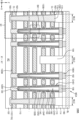
도 1은 본 발명의 기술적 사상에 의한 실시예들에 따른 집적회로 소자의 메모리 셀 어레이의 등가회로도이다.
도 2는 본 발명의 기술적 사상에 의한 실시예들에 따른 집적회로 소자의 주요 구성 요소들을 보여주는 평면도이다.
도 3a는 도 2의 X1 - X1' 선 단면도이고, 도 3b는 도 3a의 BX1으로 표시한 점선 영역의 확대 단면도이다.
도 4a 및 도 4b는 각각 본 발명의 기술적 사상에 의한 다른 실시예들에 따른 집적회로 소자의 개략적인 단면도이다.
도 5는 본 발명의 기술적 사상에 의한 또 다른 실시예들에 따른 집적회로 소자의 개략적인 단면도이다.
도 6a는 본 발명의 기술적 사상에 의한 또 다른 실시예들에 따른 집적회로 소자의 개략적인 단면도이고, 도 6b는 도 6a의 BX2으로 표시한 점선 영역의 확대 단면도이다.
도 7은 본 발명의 기술적 사상에 의한 또 다른 실시예들에 따른 집적회로 소자의 개략적인 단면도이다.
도 8a는 본 발명의 기술적 사상에 의한 또 다른 실시예들에 따른 집적회로 소자의 개략적인 단면도이고, 도 8b는 도 8a의 BX3으로 표시한 점선 영역의 확대 단면도이다.
도 9는 본 발명의 기술적 사상에 의한 또 다른 실시예들에 따른 집적회로 소자의 개략적인 단면도이다.
도 10a 및 도 10b는 각각 본 발명의 기술적 사상에 의한 또 다른 실시예들에 따른 집적회로 소자의 개략적인 단면도이다.
도 11a는 본 발명의 기술적 사상에 의한 또 다른 실시예들에 따른 집적회로 소자의 주요 영역들의 평면 레이아웃 다이어그램이고, 도 11b는 도 11a에 예시한 집적회로 소자의 일부 영역의 개략적인 사시도이고, 도 11c는 도 11a에 예시한 집적회로 소자의 일부 영역의 개략적인 단면도이다.
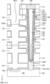
도 12a 내지 도 12m은 본 발명의 기술적 사상에 의한 실시예들에 따른 집적 회로 소자의 제조 방법을 설명하기 위하여 공정 순서에 따라 도시한 단면도들이다.
도 13a 내지 도 13i는 본 발명의 기술적 사상에 의한 다른 실시예들에 따른 집적 회로 소자의 제조 방법을 설명하기 위하여 공정 순서에 따라 도시한 단면도들이다.
도 14a 내지 도 14d는 본 발명의 기술적 사상에 의한 또 다른 실시예들에 따른 집적 회로 소자의 제조 방법을 설명하기 위하여 공정 순서에 따라 도시한 단면도들이다.
도 15a 및 도 15b는 본 발명의 기술적 사상에 의한 또 다른 실시예들에 따른 집적 회로 소자의 제조 방법을 설명하기 위하여 공정 순서에 따라 도시한 단면도들이다.
도 16은 본 발명의 기술적 사상에 의한 또 다른 실시예들에 따른 집적 회로 소자의 제조 방법을 설명하기 위하여 공정 순서에 따라 도시한 단면도이다.
도 17a 내지 도 17c는 본 발명의 기술적 사상에 의한 또 다른 실시예들에 따른 집적 회로 소자의 제조 방법을 설명하기 위하여 공정 순서에 따라 도시한 단면도들이다.
도 18a 및 도 18b는 본 발명의 기술적 사상에 의한 또 다른 실시예들에 따른 집적 회로 소자의 제조 방법을 설명하기 위하여 공정 순서에 따라 도시한 단면도들이다. FIG. 1 is an equivalent circuit diagram of a memory cell array of an integrated circuit device according to embodiments of the technical idea of the present invention.
FIG. 2 is a plan view showing major components of an integrated circuit device according to embodiments of the technical idea of the present invention.
Fig. 3a is a cross-sectional view taken along the line X1 - X1' of Fig. 2, and Fig. 3b is an enlarged cross-sectional view of the dotted line area indicated as BX1 in Fig. 3a.
FIGS. 4A and 4B are schematic cross-sectional views of integrated circuit elements according to different embodiments of the technical concept of the present invention, respectively.
FIG. 5 is a schematic cross-sectional view of an integrated circuit device according to further embodiments of the technical idea of the present invention.
FIG. 6a is a schematic cross-sectional view of an integrated circuit device according to further embodiments of the technical idea of the present invention, and FIG. 6b is an enlarged cross-sectional view of a dotted line area indicated by BX2 in FIG. 6a.
FIG. 7 is a schematic cross-sectional view of an integrated circuit device according to further embodiments of the technical idea of the present invention.
FIG. 8a is a schematic cross-sectional view of an integrated circuit device according to further embodiments of the technical idea of the present invention, and FIG. 8b is an enlarged cross-sectional view of a dotted line area indicated by BX3 in FIG. 8a.
FIG. 9 is a schematic cross-sectional view of an integrated circuit device according to further embodiments of the technical idea of the present invention.
FIGS. 10A and 10B are schematic cross-sectional views of integrated circuit elements according to further embodiments of the technical idea of the present invention, respectively.
FIG. 11a is a planar layout diagram of major regions of an integrated circuit device according to further embodiments of the technical idea of the present invention, FIG. 11b is a schematic perspective view of a portion of the integrated circuit device illustrated in FIG. 11a, and FIG. 11c is a schematic cross-sectional view of a portion of the integrated circuit device illustrated in FIG. 11a.
FIGS. 12A to 12M are cross-sectional views illustrating a manufacturing method of an integrated circuit element according to embodiments of the technical idea of the present invention in accordance with the process sequence.
FIGS. 13A to 13I are cross-sectional views illustrating a manufacturing method of an integrated circuit element according to other embodiments of the technical idea of the present invention in accordance with the process sequence.
FIGS. 14A to 14D are cross-sectional views illustrating a manufacturing method of an integrated circuit device according to further embodiments of the technical idea of the present invention in accordance with the process sequence.
FIGS. 15A and 15B are cross-sectional views illustrating a process sequence for explaining a method of manufacturing an integrated circuit device according to further embodiments of the technical idea of the present invention.
FIG. 16 is a cross-sectional view illustrating a process sequence for manufacturing an integrated circuit element according to further embodiments of the technical idea of the present invention.
FIGS. 17A to 17C are cross-sectional views illustrating a manufacturing method of an integrated circuit element according to further embodiments of the technical idea of the present invention in accordance with the process sequence.
FIGS. 18a and 18b are cross-sectional views illustrating a manufacturing method of an integrated circuit device according to further embodiments of the technical idea of the present invention in accordance with the process sequence.
이하, 첨부 도면을 참조하여 본 발명의 실시예들을 상세히 설명한다. 도면상의 동일한 구성요소에 대해서는 동일한 참조부호를 사용하고, 이들에 대한 중복된 설명은 생략한다. Hereinafter, embodiments of the present invention will be described in detail with reference to the attached drawings. The same reference numerals are used for the same components in the drawings, and redundant descriptions thereof are omitted.
도 1은 본 발명의 기술적 사상에 의한 실시예들에 따른 집적회로 소자의 메모리 셀 어레이(MCA)의 등가회로도이다. 도 1에는 수직 채널 구조를 갖는 수직형 낸드(NAND) 플래시 메모리 소자의 등가 회로도가 예시되어 있다. FIG. 1 is an equivalent circuit diagram of a memory cell array (MCA) of an integrated circuit device according to embodiments of the technical idea of the present invention. FIG. 1 illustrates an equivalent circuit diagram of a vertical NAND flash memory device having a vertical channel structure.
도 1을 참조하면, 메모리 셀 어레이(MCA)는 복수의 메모리 셀 스트링(MS)을 포함할 수 있다. 메모리 셀 어레이(MCA)는 복수의 비트 라인(BL: BL1, BL2, …, BLm), 복수의 워드 라인(WL: WL1, WL2, …, WLn-1, WLn), 적어도 하나의 스트링 선택 라인(SSL), 적어도 하나의 접지 선택 라인(GSL), 및 공통 소스 라인(CSL)을 포함할 수 있다. 복수의 비트 라인(BL: BL1, BL2, …, BLm) 및 공통 소스 라인(CSL) 사이에 복수의 메모리 셀 스트링(MS)이 형성될 수 있다. Referring to FIG. 1, a memory cell array (MCA) may include a plurality of memory cell strings (MS). The memory cell array (MCA) may include a plurality of bit lines (BL: BL1, BL2, ..., BLm), a plurality of word lines (WL: WL1, WL2, ..., WLn-1, WLn), at least one string select line (SSL), at least one ground select line (GSL), and a common source line (CSL). A plurality of memory cell strings (MS) may be formed between the plurality of bit lines (BL: BL1, BL2, ..., BLm) and the common source line (CSL).
복수의 메모리 셀 스트링(MS)은 각각 스트링 선택 트랜지스터(SST), 접지 선택 트랜지스터(GST), 및 복수의 메모리 셀 트랜지스터(MC1, MC2, …, MCn-1, MCn)를 포함할 수 있다. 스트링 선택 트랜지스터(SST)의 드레인 영역은 비트 라인(BL: BL1, BL2, …, BLm)과 연결되며, 접지 선택 트랜지스터(GST)의 소스 영역은 공통 소스 라인(CSL)과 연결될 수 있다. 공통 소스 라인(CSL)은 복수의 접지 선택 트랜지스터(GST)의 소스 영역이 공통으로 연결된 영역일 수 있다.Each of the plurality of memory cell strings (MS) may include a string select transistor (SST), a ground select transistor (GST), and a plurality of memory cell transistors (MC1, MC2, ..., MCn-1, MCn). A drain region of the string select transistor (SST) may be connected to a bit line (BL: BL1, BL2, ..., BLm), and a source region of the ground select transistor (GST) may be connected to a common source line (CSL). The common source line (CSL) may be a region to which source regions of the plurality of ground select transistors (GST) are commonly connected.
스트링 선택 트랜지스터(SST)는 스트링 선택 라인(SSL)과 연결될 수 있고, 접지 선택 트랜지스터(GST)는 접지 선택 라인(GSL)과 연결될 수 있다. 복수의 메모리 셀 트랜지스터(MC1, MC2, …, MCn-1, MCn)는 각각 복수의 워드 라인(WL: WL1, WL2, …, WLn-1, WLn)에 연결될 수 있다.A string select transistor (SST) can be connected to a string select line (SSL), and a ground select transistor (GST) can be connected to a ground select line (GSL). A plurality of memory cell transistors (MC1, MC2, …, MCn-1, MCn) can be connected to a plurality of word lines (WL: WL1, WL2, …, WLn-1, WLn), respectively.
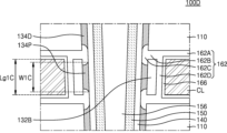
도 2는 본 발명의 기술적 사상에 의한 실시예들에 따른 집적회로 소자(100A)의 주요 구성 요소들을 보여주는 평면도이고, 도 3a는 도 2의 X1 - X1' 선 단면도이고, 도 3b는 도 3a의 BX1으로 표시한 점선 영역의 확대 단면도이다. FIG. 2 is a plan view showing main components of an integrated circuit device (100A) according to embodiments of the technical idea of the present invention, FIG. 3a is a cross-sectional view taken along line X1 - X1' of FIG. 2, and FIG. 3b is an enlarged cross-sectional view of a dotted line area indicated by BX1 of FIG. 3a.
도 2, 도 3a, 및 도 3b를 참조하면, 집적회로 소자(100A)는 활성 영역(AC)을 가지는 기판(102)을 포함한다. 기판(102)의 활성 영역(AC) 위에는 메모리 셀 어레이(MCA)가 형성될 수 있다. 메모리 셀 어레이(MCA)는 도 1을 참조하여 설명한 바와 같은 회로 구성을 가질 수 있다. Referring to FIGS. 2, 3A, and 3B, an integrated circuit device (100A) includes a substrate (102) having an active area (AC). A memory cell array (MCA) may be formed on the active area (AC) of the substrate (102). The memory cell array (MCA) may have a circuit configuration as described with reference to FIG. 1.
기판(102)은 X 방향 및 Y 방향으로 연장되는 주면(main surface)(102M)을 가질 수 있다. 예시적인 실시예들에서, 기판(102)은 Si, Ge, 또는 SiGe를 포함할 수 있다. 다른 예시적인 실시예들에서, 기판(102)은 SOI(silicon-on-insulator) 기판, 또는 GeOI(germanium-on-insulator) 기판을 포함할 수 있다. The substrate (102) can have a main surface (102M) extending in the X-direction and the Y-direction. In exemplary embodiments, the substrate (102) can include Si, Ge, or SiGe. In other exemplary embodiments, the substrate (102) can include a silicon-on-insulator (SOI) substrate, or a germanium-on-insulator (GeOI) substrate.
복수의 도전 라인(CL)이 기판(102) 상에서 주면(102M)에 평행한 수평 방향으로 X-Y 평면을 따라 연장되고, 기판(102)의 주면(102M)에 수직인 수직 방향 (Z 방향)으로 서로 이격되어 상호 중첩되도록 배치될 수 있다. 본 명세서에서, "도전 라인(CL)"은 "도전 패턴(CL)"으로 칭해질 수 있으며, "도전 라인(CL)" 및 "도전 패턴(CL)"은 동일한 구성 요소를 지칭하는 것으로 이해되어야 한다. 기판(102) 상에는 복수의 절연막(110)이 수평 방향으로 연장될 수 있다. 복수의 절연막(110)은 복수의 도전 라인(CL) 각각의 사이에 하나씩 개재될 수 있다. A plurality of conductive lines (CL) may be arranged to extend along the X-Y plane in a horizontal direction parallel to the main surface (102M) on the substrate (102) and to overlap each other while being spaced apart from each other in a vertical direction (Z direction) perpendicular to the main surface (102M) of the substrate (102). In the present specification, a "conductive line (CL)" may be referred to as a "conductive pattern (CL)", and it should be understood that "conductive line (CL)" and "conductive pattern (CL)" refer to the same component. A plurality of insulating films (110) may extend in a horizontal direction on the substrate (102). The plurality of insulating films (110) may be interposed one by one between each of the plurality of conductive lines (CL).
복수의 도전 라인(CL) 및 복수의 절연막(110)을 관통하여 복수의 채널 홀(CHH)이 형성되고, 복수의 채널 홀(CHH) 내에서 복수의 채널 구조물(CHS1)이 수직 방향(Z 방향)으로 연장될 수 있다. 복수의 채널 구조물(CHS1)은 각각 기판(102)에 접하고 채널 홀(CHH)을 부분적으로 채우는 반도체 패턴(120)과, 반도체 패턴(120)에 접하고 채널 홀(CHH) 내에서 수직 방향(Z 방향)으로 연장되는 채널막(150)과, 채널막(150)의 내부 공간을 채우는 매립 절연막(156)과, 채널막(150)에 접하고 채널 홀(CHH)의 입구측 상부를 채우는 드레인 영역(158)를 포함할 수 있다. 예시적인 실시예들에서, 채널막(150)은 내부 공간을 가지는 실린더 형상을 가질 수 있으며, 채널막(150)의 내부 공간은 매립 절연막(156)으로 채워질 수 있다. 채널막(150)은 도핑된 폴리실리콘, 또는 도핑되지 않은 폴리실리콘으로 이루어질 수 있다. 매립 절연막(156)은 실리콘 산화물, 실리콘 질화물, 실리콘 산질화물, 또는 이들의 조합으로 이루어질 수 있다. 예시적인 실시예들에서 매립 절연막(156)은 생략 가능하며, 이 경우 채널막(150)은 내부 공간이 없는 필라(pillar) 구조를 가질 수 있다. 드레인 영역(158)은 도핑된 폴리실리콘막으로 이루어질 수 있다. 복수의 드레인 영역(158)은 절연 패턴(114)에 의해 상호 절연될 수 있다. 절연 패턴(114)은 산화막, 질화막, 또는 이들의 조합으로 이루어질 수 있다. A plurality of channel holes (CHH) are formed by penetrating a plurality of conductive lines (CL) and a plurality of insulating films (110), and a plurality of channel structures (CHS1) may extend in a vertical direction (Z direction) within the plurality of channel holes (CHH). The plurality of channel structures (CHS1) may each include a semiconductor pattern (120) that contacts the substrate (102) and partially fills the channel hole (CHH), a channel film (150) that contacts the semiconductor pattern (120) and extends in a vertical direction (Z direction) within the channel hole (CHH), a buried insulating film (156) that fills an internal space of the channel film (150), and a drain region (158) that contacts the channel film (150) and fills an upper portion of an inlet side of the channel hole (CHH). In exemplary embodiments, the channel film (150) may have a cylindrical shape having an internal space, and the internal space of the channel film (150) may be filled with the buried insulating film (156). The channel film (150) may be made of doped polysilicon or undoped polysilicon. The buried insulating film (156) may be made of silicon oxide, silicon nitride, silicon oxynitride, or a combination thereof. In exemplary embodiments, the buried insulating film (156) may be omitted, in which case the channel film (150) may have a pillar structure without an internal space. The drain region (158) may be made of a doped polysilicon film. A plurality of drain regions (158) may be mutually insulated by an insulating pattern (114). The insulating pattern (114) may be made of an oxide film, a nitride film, or a combination thereof.
복수의 채널 구조물(CHS1)은 복수의 전하 트랩 패턴(134P)과, 복수의 더미 전하 트랩 패턴(134D)을 포함한다. 본 명세서에서 사용되는 용어 "전하 트랩 패턴" 및 "더미 전하 트랩 패턴"은 각각 "전하 저장 패턴" 및 "더미 전하 저장 패턴"으로 칭해질 수 있으며, 용어 "전하 트랩 패턴" 및 "전하 저장 패턴"은 동일한 의미로 사용된다. 복수의 전하 트랩 패턴(134P)은 각각 서로 이격된 상태로 채널 홀(CHH) 내에서 도전 라인(CL)과 채널막(150)과의 사이에 개재될 수 있다. 복수의 더미 전하 트랩 패턴(134D)은 복수의 전하 트랩 패턴(134P)으로부터 이격된 위치에서 절연막(110)과 채널막(150)의 사이에 개재될 수 있다. 복수의 더미 전하 트랩 패턴(134D)은 서로 이격되어 있으며, 복수의 더미 전하 트랩 패턴(134D) 각각의 사이에는 하나의 전하 트랩 패턴(134P)이 개재될 수 있다. 복수의 전하 트랩 패턴(134P) 및 복수의 더미 전하 트랩 패턴(134D)은 채널 홀(CHH) 내에서 기판(102)으로부터 멀어지는 방향으로 연장되는 일직선을 따라 연장되고, 상기 일직선을 따라 하나씩 교대로 배치될 수 있다. 복수의 전하 트랩 패턴(134P) 및 복수의 더미 전하 트랩 패턴(134D)은 수평 방향에서 서로 동일한 폭을 가질 수 있다. 복수의 전하 트랩 패턴(134P) 및 복수의 더미 전하 트랩 패턴(134D)은 각각 상기 일직선을 따라 일정한 폭을 가질 수 있다. 예를 들면, 복수의 전하 트랩 패턴(134P) 및 복수의 더미 전하 트랩 패턴(134D)은 각각 수평 방향에서 약 3 ∼ 10 nm의 폭을 가질 수 있다. The plurality of channel structures (CHS1) include a plurality of charge trap patterns (134P) and a plurality of dummy charge trap patterns (134D). The terms “charge trap pattern” and “dummy charge trap pattern” used in the present specification may be referred to as “charge storage pattern” and “dummy charge storage pattern”, respectively, and the terms “charge trap pattern” and “charge storage pattern” are used with the same meaning. The plurality of charge trap patterns (134P) may be interposed between the conductive line (CL) and the channel film (150) within the channel hole (CHH) while being spaced apart from each other. The plurality of dummy charge trap patterns (134D) may be interposed between the insulating film (110) and the channel film (150) at a position spaced apart from the plurality of charge trap patterns (134P). A plurality of dummy charge trap patterns (134D) are spaced apart from each other, and a single charge trap pattern (134P) may be interposed between each of the plurality of dummy charge trap patterns (134D). The plurality of charge trap patterns (134P) and the plurality of dummy charge trap patterns (134D) may extend along a straight line extending away from the substrate (102) within the channel hole (CHH), and may be alternately arranged one by one along the straight line. The plurality of charge trap patterns (134P) and the plurality of dummy charge trap patterns (134D) may have the same width in the horizontal direction. The plurality of charge trap patterns (134P) and the plurality of dummy charge trap patterns (134D) may each have a constant width along the straight line. For example, the plurality of charge trap patterns (134P) and the plurality of dummy charge trap patterns (134D) may each have a width of about 3 to 10 nm in the horizontal direction.
수평 방향에서 복수의 전하 트랩 패턴(134P)과 채널막(150)과의 사이의 최소 이격 거리는 복수의 더미 전하 트랩 패턴(134D)과 채널막(150)과의 사이의 최소 이격 거리와 실질적으로 동일할 수 있다. 복수의 전하 트랩 패턴(134P) 및 복수의 더미 전하 트랩 패턴(134D)은 각각 실리콘 질화막으로 이루어질 수 있다. The minimum separation distance between the plurality of charge trap patterns (134P) and the channel film (150) in the horizontal direction may be substantially the same as the minimum separation distance between the plurality of dummy charge trap patterns (134D) and the channel film (150). The plurality of charge trap patterns (134P) and the plurality of dummy charge trap patterns (134D) may each be formed of a silicon nitride film.
수직 방향에서 전하 트랩 패턴(134P)의 길이(W1)는 도전 라인(CL)의 길이(Lg1) 이하이고, 도전 라인(CL)의 길이(Lg1)의 1/2 이상일 수 있다. 전하 트랩 패턴(134P)은 도전 라인(CL) 중 절연막(110)에 가장 가까운 코너에 대면하는 부분을 포함하지 않을 수 있다. 따라서, 도전 라인(CL)의 코너에 집중되는 전계로 인해 전하 트랩 패턴(134P)에 미치는 악영향을 최소화할 수 있다. In the vertical direction, the length (W1) of the charge trap pattern (134P) may be less than or equal to the length (Lg1) of the conductive line (CL), and may be more than half the length (Lg1) of the conductive line (CL). The charge trap pattern (134P) may not include a portion facing the corner of the conductive line (CL) closest to the insulating film (110). Accordingly, the adverse effect on the charge trap pattern (134P) due to the electric field concentrated at the corner of the conductive line (CL) can be minimized.
복수의 도전 라인(CL)과 채널 구조물(CHS1)과의 사이에 복수의 제1 블로킹 유전 패턴(132B)이 배치될 수 있다. 복수의 제1 블로킹 유전 패턴(132B)은 복수의 절연막(110) 각각의 사이에 하나씩 배치될 수 있다. 복수의 제1 블로킹 유전 패턴(132B) 각각의 일부는 복수의 절연막(110)과 수직으로 오버랩될 수 있다. 복수의 제1 블로킹 유전 패턴(132B)은 각각 도전 라인(CL)과 전하 트랩 패턴(134P)과의 사이에 개재될 수 있다. 복수의 제1 블로킹 유전 패턴(132B) 중 채널막(150)에 대면하는 측벽은 전하 트랩 패턴(134P) 중 도전 라인(CL)과 대면하는 측벽에 접하고, 복수의 절연막(110) 중 채널막(150)에 대면하는 측벽들과 일직선 상에 연장될 수 있다. 복수의 제1 블로킹 유전 패턴(132B)은 실리콘 산화막으로 이루어질 수 있다. 복수의 제1 블로킹 유전 패턴(132B)의 수평 방향 폭은 약 3 ∼ 10 nm, 예를 들면 약 3 ∼ 5 nm 일 수 있다. A plurality of first blocking dielectric patterns (132B) may be arranged between a plurality of conductive lines (CL) and a channel structure (CHS1). The plurality of first blocking dielectric patterns (132B) may be arranged one by one between each of the plurality of insulating films (110). A portion of each of the plurality of first blocking dielectric patterns (132B) may vertically overlap with the plurality of insulating films (110). The plurality of first blocking dielectric patterns (132B) may be interposed between the conductive lines (CL) and the charge trap patterns (134P), respectively. A sidewall of the plurality of first blocking dielectric patterns (132B) facing the channel film (150) may be in contact with a sidewall of the charge trap patterns (134P) facing the conductive lines (CL) and may extend in a straight line with sidewalls of the plurality of insulating films (110) facing the channel film (150). The plurality of first blocking dielectric patterns (132B) may be formed of a silicon oxide film. The horizontal width of the plurality of first blocking dielectric patterns (132B) may be about 3 to 10 nm, for example, about 3 to 5 nm.
복수의 절연막(110) 각각의 사이에는 제1 블로킹 유전 패턴(132B)의 일부와 도전 라인(CL)의 일부를 감싸는 제2 블로킹 유전 패턴(162)이 형성될 수 있다. 제2 블로킹 유전 패턴(162)은 도전 라인(CL)과 절연막(110)과의 사이에 개재된 제1 부분(162A), 제1 블로킹 유전 패턴(132B)과 절연막(110)과의 사이에 개재된 제2 부분(162B), 전하 트랩 패턴(134P)과 더미 전하 트랩 패턴(134D)과의 사이에 개재된 제3 부분(162C), 및 도전 라인(CL)과 제1 블로킹 유전 패턴(132B)과의 사이에 개재된 제4 부분(162D)을 포함할 수 있다. 제2 블로킹 유전 패턴(162)의 제1 부분(162A), 제2 부분(162B), 제3 부분(162C), 및 제4 부분(162D)은 일체로 연결될 수 있다. 제2 블로킹 유전 패턴(162)의 제3 부분(162C)은 복수의 전하 트랩 패턴(134P) 및 복수의 더미 전하 트랩 패턴(134D) 각각의 사이의 이격 공간을 채우며, 전하 트랩 패턴(134P) 및 더미 전하 트랩 패턴(134D)에 접할 수 있다. 제2 블로킹 유전 패턴(162)은 실리콘 산화막, 고유전막, 또는 이들의 조합으로 이루어질 수 있다. 상기 금속 산화막은 실리콘 산화막보다 높은 유전 상수를 가지는 고유전막으로 이루어질 수 있다. 예를 들면, 상기 고유전막은 HfO2, Al2O3, 또는 ZrO2로 이루어질 수 있으나, 이들에 한정되지 않는다.Between each of the plurality of insulating films (110), a second blocking dielectric pattern (162) may be formed that surrounds a portion of the first blocking dielectric pattern (132B) and a portion of the conductive line (CL). The second blocking dielectric pattern (162) may include a first portion (162A) interposed between the conductive line (CL) and the insulating film (110), a second portion (162B) interposed between the first blocking dielectric pattern (132B) and the insulating film (110), a third portion (162C) interposed between the charge trap pattern (134P) and the dummy charge trap pattern (134D), and a fourth portion (162D) interposed between the conductive line (CL) and the first blocking dielectric pattern (132B). The first portion (162A), the second portion (162B), the third portion (162C), and the fourth portion (162D) of the second blocking dielectric pattern (162) can be connected integrally. The third portion (162C) of the second blocking dielectric pattern (162) fills a space between each of the plurality of charge trap patterns (134P) and the plurality of dummy charge trap patterns (134D), and can contact the charge trap patterns (134P) and the dummy charge trap patterns (134D). The second blocking dielectric pattern (162) can be formed of a silicon oxide film, a high-k dielectric film, or a combination thereof. The metal oxide film can be formed of a high-k dielectric film having a higher dielectric constant than the silicon oxide film. For example, the high-k dielectric film can be formed of, but is not limited to, HfO 2 , Al 2 O 3 , or ZrO 2 .
복수의 제1 블로킹 유전 패턴(132B)과 채널막(150)과의 사이에 전하 트랩 패턴(134P) 및 터널링 유전막(140)이 개재될 수 있다. 터널링 유전막(140)은 전하 트랩 패턴(134P)과 채널막(150)과의 사이, 및 더미 전하 트랩 패턴(134D)과 채널막(150)과의 사이를 지나면서 채널막(150)의 연장 방향을 따라 길게 연장될 수 있다. 전하 트랩 패턴(134P)은 실리콘 산화막으로 이루어질 수 있다. 전하 트랩 패턴(134P) 및 채널막(150) 각각의 수평 방향 폭은 그 길이 방향을 따라 일정할 수 있다. 예를 들면, 전하 트랩 패턴(134P) 및 채널막(150) 각각의 수평 방향 폭은 약 3 ∼ 10 nm일 수 있다. A charge trap pattern (134P) and a tunneling dielectric film (140) may be interposed between a plurality of first blocking dielectric patterns (132B) and the channel film (150). The tunneling dielectric film (140) may extend long along the extension direction of the channel film (150) while passing between the charge trap pattern (134P) and the channel film (150) and between the dummy charge trap pattern (134D) and the channel film (150). The charge trap pattern (134P) may be formed of a silicon oxide film. The horizontal width of each of the charge trap pattern (134P) and the channel film (150) may be constant along the longitudinal direction. For example, the horizontal width of each of the charge trap pattern (134P) and the channel film (150) may be about 3 to about 10 nm.
복수의 도전 라인(CL) 및 복수의 절연막(110) 각각의 제1 수평 방향(X 방향)의 폭은 복수의 워드 라인 컷 영역(WLC)에 의해 한정될 수 있다. 복수의 도전 라인(CL)은 복수의 워드 라인 컷 영역(WLC)에 의해 일정 간격으로 상호 이격되어 반복적으로 배치될 수 있다. The width of each of the plurality of conductive lines (CL) and the plurality of insulating films (110) in the first horizontal direction (X direction) may be defined by the plurality of word line cut regions (WLC). The plurality of conductive lines (CL) may be repeatedly arranged at regular intervals from each other by the plurality of word line cut regions (WLC).
기판(102)에는 복수의 공통 소스 영역(160)이 제2 수평 방향(Y 방향)을 따라 연장될 수 있다. 복수의 공통 소스 영역(160)은 n 형 불순물이 고농도로 도핑된 불순물 영역일 수 있다. 복수의 워드 라인 컷 영역(WLC)의 일부는 공통 소스 패턴(CSP)으로 채워질 수 있다. 공통 소스 패턴(CSP)은 도 1에 예시한 공통 소스 라인(CSL)을 구성할 수 있다. 공통 소스 패턴(CSP)은 복수의 공통 소스 영역(160) 상에서 제2 수평 방향(Y 방향)으로 길게 연장될 수 있다. 워드 라인 컷 영역(WLC) 내에는 공통 소스 패턴(CSP)의 측벽을 덮는 절연 스페이서(170)가 형성될 수 있다. 절연 스페이서(170)는 공통 소스 패턴(CSP)과 복수의 도전 라인(CL)과의 사이를 전기적으로 절연시키는 역할을 할 수 있다. 공통 소스 패턴(CSP) 및 절연 스페이서(170)는 캡핑 절연막(172)으로 덮일 수 있다. 공통 소스 패턴(CSP)은 텅스텐, 구리, 또는 알루미늄 등과 같은 금속; 질화티타늄, 질화탄탈럼 등과 같은 도전성 금속질화물; 티타늄, 탄탈럼 등과 같은 전이 금속; 또는 이들의 조합으로 이루어질 수 있다. 절연 스페이서(170) 및 캡핑 절연막(172)은 각각 실리콘 산화막, 실리콘 질화막, 실리콘 산질화막, 또는 이들의 조합으로 이루어질 수 있다. 공통 소스 영역(160)과 공통 소스 패턴(CSP)과의 사이에는 접촉 저항을 낮추기 위한 금속 실리사이드막(도시 생략)이 개재될 수 있다. 예를 들면, 상기 금속 실리사이드막은 코발트 실리사이드, 텅스텐 실리사이드, 니켈 실리사이드 등으로 이루어질 수 있다. A plurality of common source regions (160) may extend along a second horizontal direction (Y direction) on the substrate (102). The plurality of common source regions (160) may be impurity regions doped with a high concentration of n-type impurities. Part of the plurality of word line cut regions (WLC) may be filled with a common source pattern (CSP). The common source pattern (CSP) may form a common source line (CSL) as illustrated in FIG. 1. The common source pattern (CSP) may extend long in the second horizontal direction (Y direction) on the plurality of common source regions (160). An insulating spacer (170) covering a sidewall of the common source pattern (CSP) may be formed within the word line cut region (WLC). The insulating spacer (170) may serve to electrically insulate between the common source pattern (CSP) and the plurality of conductive lines (CL). The common source pattern (CSP) and the insulating spacer (170) may be covered with a capping insulating film (172). The common source pattern (CSP) may be made of a metal such as tungsten, copper, or aluminum; a conductive metal nitride such as titanium nitride or tantalum nitride; a transition metal such as titanium or tantalum; or a combination thereof. The insulating spacer (170) and the capping insulating film (172) may each be made of a silicon oxide film, a silicon nitride film, a silicon oxynitride film, or a combination thereof. A metal silicide film (not shown) may be interposed between the common source region (160) and the common source pattern (CSP) to lower contact resistance. For example, the metal silicide film may be made of cobalt silicide, tungsten silicide, nickel silicide, or the like.
이웃하는 2 개의 워드 라인 컷 영역(WLC) 사이에 있는 복수의 도전 라인(CL)은 도 1을 참조하여 설명한 접지 선택 라인(GSL), 복수의 워드 라인(WL: WL1, WL2, …, WLn-1, WLn), 및 스트링 선택 라인(SSL)을 구성할 수 있다. 기판(102) 상에 Z 방향을 따라 적층되는 복수의 도전 라인(CL)의 수는 필요에 따라 다양하게 선택될 수 있다. 예를 들면, 복수의 도전 라인(CL) 중 기판(102)에 가장 가까운 도전 라인(CL)은 접지 선택 라인(GSL)을 구성할 수 있다. 복수의 도전 라인(CL) 중 기판(102)으로부터 가장 먼 2 개의 도전 라인(CL)은 각각 스트링 선택 라인(SSL)을 구성할 수 있다. 스트링 선택 라인(SSL)은 스트링 선택 라인 컷 영역(SSLC)에 의해 이격된 부분을 포함할 수 있다. 스트링 선택 라인 컷 영역(SSLC)은 절연막(184)으로 채워질 수 있다. 절연막(184)은 산화막, 질화막, 에어 갭, 또는 이들의 조합으로 이루어질 수 있다. 본 명세서에서 사용되는 용어 "에어 갭"은 대기 또는 제조 공정 중에 존재할 수 있는 다른 가스들을 포함하는 공간을 의미할 수 있다. A plurality of conductive lines (CL) between two adjacent word line cut regions (WLC) can form a ground select line (GSL), a plurality of word lines (WL: WL1, WL2, ..., WLn-1, WLn), and a string select line (SSL) described with reference to FIG. 1. The number of the plurality of conductive lines (CL) stacked along the Z direction on the substrate (102) can be variously selected as needed. For example, the conductive line (CL) closest to the substrate (102) among the plurality of conductive lines (CL) can form a ground select line (GSL). Two conductive lines (CL) farthest from the substrate (102) among the plurality of conductive lines (CL) can each form a string select line (SSL). The string select line (SSL) can include a portion separated by a string select line cut region (SSLC). The string select line cut region (SSLC) can be filled with an insulating film (184). The insulating film (184) may be formed of an oxide film, a nitride film, an air gap, or a combination thereof. The term "air gap" as used herein may mean a space containing the atmosphere or other gases that may be present during the manufacturing process.
복수의 도전 라인(CL)은 텅스텐, 니켈, 코발트, 탄탈럼 등과 같은 금속, 텅스텐 실리사이드, 니켈 실리사이드, 코발트 실리사이드, 탄탈럼 실리사이드 등과 같은 금속 실리사이드, 도핑된 폴리실리콘, 또는 이들의 조합을 포함할 수 있다. The plurality of challenge lines (CL) may include metals such as tungsten, nickel, cobalt, tantalum, etc., metal silicides such as tungsten silicide, nickel silicide, cobalt silicide, tantalum silicide, etc., doped polysilicon, or combinations thereof.
메모리 셀 어레이(MCA)에서, 복수의 채널 구조물(CHS1) 상에 복수의 비트 라인(BL)이 제1 수평 방향(X 방향)으로 연장될 수 있다. 복수의 채널 구조물(CHS1)과 복수의 비트 라인(BL)과의 사이에는 복수의 비트 라인 콘택 패드(182)가 개재될 수 있다. 복수의 채널 구조물(CHS1) 각각의 드레인 영역(158)은 비트 라인 콘택 패드(182)를 통해 복수의 비트 라인(BL) 중 대응하는 하나의 비트 라인(BL)에 연결될 수 있다. 복수의 비트 라인 콘택 패드(182)는 절연막(180)에 의해 상호 절연될 수 있다. 절연막(180)은 산화막, 질화막, 또는 이들의 조합으로 이루어질 수 있다. In a memory cell array (MCA), a plurality of bit lines (BL) may extend in a first horizontal direction (X direction) on a plurality of channel structures (CHS1). A plurality of bit line contact pads (182) may be interposed between the plurality of channel structures (CHS1) and the plurality of bit lines (BL). A drain region (158) of each of the plurality of channel structures (CHS1) may be connected to a corresponding one of the plurality of bit lines (BL) through the bit line contact pad (182). The plurality of bit line contact pads (182) may be mutually insulated by an insulating film (180). The insulating film (180) may be formed of an oxide film, a nitride film, or a combination thereof.
도 3a 및 도 3b에 예시한 집적회로 소자(100A)는 복수의 전하 트랩 패턴(134P)이 채널 홀(CHH) 내에 배치되어 있으므로 복수의 전하 트랩 패턴(134P)이 채널 홀(CHH)의 외부에 있는 경우에 비해 수평 방향 및 수직 방향으로 고도로 스케일링된 집적회로 소자를 구현하는 데 유리하게 채용될 수 있다. 또한, 하나의 채널 홀(CHH) 내에서 복수의 전하 트랩 패턴(134P)이 더미 전하 트랩 패턴(134D) 및 제2 블로킹 유전 패턴(162)을 사이에 두고 수직 방향(Z 방향)으로 서로 이격되어 있다. 따라서, 수직형 메모리 소자에서 수직 방향으로 서로 인접한 셀들 사이의 간격이 비교적 작은 경우에도 인접한 셀들 사이의 전하 확산에 의한 셀 간섭을 억제하여 신뢰성을 향상시킬 수 있는 구조를 제공할 수 있다. The integrated circuit device (100A) illustrated in FIGS. 3A and 3B can be advantageously employed to implement a highly scaled integrated circuit device in the horizontal and vertical directions since a plurality of charge trap patterns (134P) are arranged within the channel hole (CHH), compared to a case where the plurality of charge trap patterns (134P) are outside the channel hole (CHH). In addition, the plurality of charge trap patterns (134P) are spaced apart from each other in the vertical direction (Z direction) with the dummy charge trap pattern (134D) and the second blocking dielectric pattern (162) interposed therebetween. Accordingly, even when the gap between cells vertically adjacent to each other in a vertical memory device is relatively small, a structure can be provided that can suppress cell interference due to charge diffusion between adjacent cells, thereby improving reliability.
도 4a는 본 발명의 기술적 사상에 의한 다른 실시예들에 따른 집적회로 소자(100B)의 개략적인 단면도이다. 도 4a에는 도 3a에서 BX1으로 표시한 점선 영역에 대응하는 부분의 확대된 단면 구성이 예시되어 있다. Fig. 4a is a schematic cross-sectional view of an integrated circuit device (100B) according to other embodiments of the technical idea of the present invention. Fig. 4a illustrates an enlarged cross-sectional configuration of a portion corresponding to a dotted line area indicated as BX1 in Fig. 3a.
도 4a를 참조하면, 집적회로 소자(100B)는 도 3a 및 도 3b에 예시한 집적회로 소자(100A)와 대체로 동일한 구성을 가진다. 단, 집적회로 소자(100B)에서 복수의 제1 블로킹 유전 패턴(132B) 각각은 제2 블로킹 유전 패턴(162)과 일체로 연결될 수 있다. 제1 블로킹 유전 패턴(132B)은 "제1 패턴 부분"으로 칭해지고, 제2 블로킹 유전 패턴(162)은 "제2 패턴 부분"으로 칭해질 수 있다. 도 4a에서, 제1 블로킹 유전 패턴(132B)과 제2 블로킹 유전 패턴(162)이 점선(DL)으로 표시한 가상선으로 구분되어 있으나, 실제로는 제1 블로킹 유전 패턴(132B)과 제2 블로킹 유전 패턴(162)과의 사이에 가시적인 계면 없이 상호 연결되어 있을 수 있다. 집적회로 소자(100B)에서, 복수의 제1 블로킹 유전 패턴(132B) 및 복수의 제2 블로킹 유전 패턴(162)은 동일한 물질로 이루어질 수 있다. 일 예에서, 복수의 제1 블로킹 유전 패턴(132B) 및 복수의 제2 블로킹 유전 패턴(162)은 각각 실리콘 산화막으로 이루어질 수 있다. 다른 예에서, 복수의 제1 블로킹 유전 패턴(132B) 및 복수의 제2 블로킹 유전 패턴(162)은 각각 동일한 물질의 고유전막으로 이루어질 수 있다. 상기 고유전막은 HfO2, Al2O3, 또는 ZrO2로 이루어질 수 있으나, 이들에 한정되는 것은 아니다. Referring to FIG. 4A, the integrated circuit device (100B) has substantially the same configuration as the integrated circuit device (100A) illustrated in FIGS. 3A and 3B. However, in the integrated circuit device (100B), each of the plurality of first blocking dielectric patterns (132B) may be integrally connected to the second blocking dielectric pattern (162). The first blocking dielectric pattern (132B) may be referred to as a “first pattern portion”, and the second blocking dielectric pattern (162) may be referred to as a “second pattern portion”. In FIG. 4A, the first blocking dielectric pattern (132B) and the second blocking dielectric pattern (162) are separated by a virtual line indicated by a dotted line (DL), but in reality, the first blocking dielectric pattern (132B) and the second blocking dielectric pattern (162) may be interconnected without a visible interface therebetween. In the integrated circuit device (100B), the plurality of first blocking dielectric patterns (132B) and the plurality of second blocking dielectric patterns (162) may be formed of the same material. In one example, the plurality of first blocking dielectric patterns (132B) and the plurality of second blocking dielectric patterns (162) may each be formed of a silicon oxide film. In another example, the plurality of first blocking dielectric patterns (132B) and the plurality of second blocking dielectric patterns (162) may each be formed of a high-k dielectric film of the same material. The high-k dielectric film may be formed of, but is not limited to, HfO 2 , Al 2 O 3 , or ZrO 2 .
도 4b는 본 발명의 기술적 사상에 의한 또 다른 실시예들에 따른 집적회로 소자(100C)의 개략적인 단면도이다. 도 4b에는 도 3a에서 BX1으로 표시한 점선 영역에 대응하는 부분의 확대된 단면 구성이 예시되어 있다. Fig. 4b is a schematic cross-sectional view of an integrated circuit device (100C) according to further embodiments of the technical idea of the present invention. Fig. 4b illustrates an enlarged cross-sectional configuration of a portion corresponding to the dotted line area indicated by BX1 in Fig. 3a.
도 4b를 참조하면, 집적회로 소자(100C)는 도 3a 및 도 3b에 예시한 집적회로 소자(100A)와 대체로 동일한 구성을 가진다. 단, 집적회로 소자(100C)는 제2 블로킹 유전 패턴(164)을 포함한다. 제2 블로킹 유전 패턴(164)은 도 3a 및 도 3b에 예시한 제2 블로킹 유전 패턴(162)과 대체로 동일한 구성을 가진다. 단, 제2 블로킹 유전 패턴(164)의 제3 부분(162C)에는 에어 갭(AG1)이 포함될 수 있다. 에어 갭(AG1)의 단면 형상은 도 4b에 예시한 바에 한정되는 것은 아니다. 에어 갭(AG1)은 다양한 폭 및 높이를 가질 수 있다. 제2 블로킹 유전 패턴(164)의 제3 부분(162C)에 에어 갭(AG1)이 포함됨으로써, 복수의 전하 트랩 패턴(134P) 각각의 사이의 유전율이 더욱 낮아질 수 있으며, 수직형 메모리 소자에서 인접한 셀들 사이의 전하 확산에 의한 셀 간섭 억제 효과를 더욱 향상시킬 수 있다. Referring to FIG. 4B, the integrated circuit device (100C) has substantially the same configuration as the integrated circuit device (100A) illustrated in FIGS. 3A and 3B. However, the integrated circuit device (100C) includes a second blocking dielectric pattern (164). The second blocking dielectric pattern (164) has substantially the same configuration as the second blocking dielectric pattern (162) illustrated in FIGS. 3A and 3B. However, an air gap (AG1) may be included in a third portion (162C) of the second blocking dielectric pattern (164). The cross-sectional shape of the air gap (AG1) is not limited to that illustrated in FIG. 4B. The air gap (AG1) may have various widths and heights. By including an air gap (AG1) in the third portion (162C) of the second blocking dielectric pattern (164), the dielectric constant between each of the plurality of charge trap patterns (134P) can be further reduced, and the effect of suppressing cell interference due to charge diffusion between adjacent cells in a vertical memory device can be further improved.
도 4b에 예시한 집적회로 소자(100C)에서, 도 4a를 참조하여 제1 블로킹 유전 패턴(132B)과 제2 블로킹 유전 패턴(162)과의 사이의 계면에 대하여 설명한 바와 유사하게, 제1 블로킹 유전 패턴(132B)과 제2 블로킹 유전 패턴(164)과의 사이에 가시적인 계면은 없을 수 있다. 이 경우, 복수의 제1 블로킹 유전 패턴(132B)과 복수의 제2 블로킹 유전 패턴(164)은 동일한 물질로 이루어질 수 있다. In the integrated circuit element (100C) illustrated in FIG. 4B, similarly to the interface between the first blocking dielectric pattern (132B) and the second blocking dielectric pattern (162) described with reference to FIG. 4A, there may be no visible interface between the first blocking dielectric pattern (132B) and the second blocking dielectric pattern (164). In this case, the plurality of first blocking dielectric patterns (132B) and the plurality of second blocking dielectric patterns (164) may be formed of the same material.
도 5는 본 발명의 기술적 사상에 의한 또 다른 실시예들에 따른 집적회로 소자(100D)의 개략적인 단면도이다. 도 5에는 도 3a에서 BX1으로 표시한 점선 영역에 대응하는 부분의 확대된 단면 구성이 예시되어 있다. Fig. 5 is a schematic cross-sectional view of an integrated circuit device (100D) according to further embodiments of the technical idea of the present invention. Fig. 5 illustrates an enlarged cross-sectional configuration of a portion corresponding to a dotted line area indicated by BX1 in Fig. 3a.
도 5를 참조하면, 집적회로 소자(100D)는 도 3a 및 도 3b에 예시한 집적회로 소자(100A)와 대체로 동일한 구성을 가진다. 단, 집적회로 소자(100D)는 복수의 제3 블로킹 유전 패턴(166)을 더 포함한다. 복수의 제3 블로킹 유전 패턴(166)은 각각 도전 라인(CL)과 제2 블로킹 유전 패턴(162)과의 사이에 개재되어 있다. 복수의 제3 블로킹 유전 패턴(166)은 각각 실리콘 산화막, 고유전막, 또는 이들의 조합으로 이루어질 수 있다. 상기 고유전막은 HfO2, Al2O3, 또는 ZrO2로 이루어질 수 있으나, 이들에 한정되는 것은 아니다. 일 예에서, 복수의 제2 블로킹 유전 패턴(162)은 실리콘 산화막으로 이루어지고, 복수의 제3 블로킹 유전 패턴(166)은 고유전막으로 이루어질 수 있다. 다른 예에서, 복수의 제2 블로킹 유전 패턴(162)은 고유전막으로 이루어지고, 복수의 제3 블로킹 유전 패턴(166)은 실리콘 산화막으로 이루어질 수 있다. Referring to FIG. 5, the integrated circuit device (100D) has substantially the same configuration as the integrated circuit device (100A) illustrated in FIGS. 3A and 3B. However, the integrated circuit device (100D) further includes a plurality of third blocking dielectric patterns (166). The plurality of third blocking dielectric patterns (166) are each interposed between the conductive line (CL) and the second blocking dielectric pattern (162). The plurality of third blocking dielectric patterns (166) may each be formed of a silicon oxide film, a high-k dielectric film, or a combination thereof. The high-k dielectric film may be formed of, but is not limited to, HfO 2 , Al 2 O 3 , or ZrO 2 . In one example, the plurality of second blocking dielectric patterns (162) may be formed of a silicon oxide film, and the plurality of third blocking dielectric patterns (166) may be formed of a high-k dielectric film. In another example, the plurality of second blocking dielectric patterns (162) may be formed of a high-k dielectric film, and the plurality of third blocking dielectric patterns (166) may be formed of a silicon oxide film.
집적회로 소자(100D)에서, 전하 트랩 패턴(134P)의 수직 방향 길이(W1C)는 도전 라인(CL)의 수직 방향 길이(Lg1C) 이하이고, 도전 라인(CL)의 길이(Lg1C)의 1/2 이상일 수 있다. In the integrated circuit device (100D), the vertical length (W1C) of the charge trap pattern (134P) may be less than or equal to the vertical length (Lg1C) of the conductive line (CL), and may be more than half the length (Lg1C) of the conductive line (CL).
도 5에는 집적회로 소자(100D)가 도 3a 및 도 3b에 예시한 집적회로 소자(100A)와 동일한 구성에 제3 블로킹 유전 패턴(166)을 더 포함하는 경우를 예로 들어 설명하였으나, 본 발명의 기술적 사상인 이에 한정되지 않는다. 예를 들면, 도 4b를 참조하여 설명한 집적회로 소자(100C)와 동일한 구성에 도 5에 예시한 제3 블로킹 유전 패턴(166)이 더 포함될 수도 있다. 또한, 도 5에 예시한 집적회로 소자(100D)에서, 도 4a를 참조하여 설명한 바와 유사하게, 제1 블로킹 유전 패턴(132B)과 제2 블로킹 유전 패턴(162)과의 사이의 계면은 없을 수 있다. 이 경우, 복수의 제1 블로킹 유전 패턴(132B)과 복수의 제2 블로킹 유전 패턴(162)은 동일한 물질로 이루어질 수 있다. Although FIG. 5 illustrates an example in which the integrated circuit device (100D) further includes a third blocking dielectric pattern (166) in the same configuration as the integrated circuit device (100A) illustrated in FIGS. 3A and 3B, the technical idea of the present invention is not limited thereto. For example, the integrated circuit device (100C) illustrated with reference to FIG. 4B may further include a third blocking dielectric pattern (166) illustrated in FIG. 5. In addition, in the integrated circuit device (100D) illustrated in FIG. 5, similarly to what was illustrated with reference to FIG. 4A, there may be no interface between the first blocking dielectric pattern (132B) and the second blocking dielectric pattern (162). In this case, the plurality of first blocking dielectric patterns (132B) and the plurality of second blocking dielectric patterns (162) may be made of the same material.
도 6a는 본 발명의 기술적 사상에 의한 또 다른 실시예들에 따른 집적회로 소자의 개략적인 단면도이고, 도 6b는 도 6a의 BX2으로 표시한 점선 영역의 확대 단면도이다. 도 6a에는 도 2의 X1 - X1' 선 단면에 대응하는 부분의 단면 구성이 예시되어 있다. FIG. 6A is a schematic cross-sectional view of an integrated circuit device according to still other embodiments of the technical idea of the present invention, and FIG. 6B is an enlarged cross-sectional view of a dotted line area indicated by BX2 in FIG. 6A. FIG. 6A illustrates an example of a cross-sectional configuration of a portion corresponding to the cross-section along line X1 - X1' in FIG. 2.
도 6a 및 도 6b를 참조하면, 집적회로 소자(200A)는 도 3a 및 도 3b에 예시한 집적회로 소자(100A)와 대체로 동일한 구성을 가진다. 단, 집적회로 소자(200A)는 복수의 채널 구조물(CHS2)을 포함한다. Referring to FIGS. 6A and 6B, the integrated circuit device (200A) has substantially the same configuration as the integrated circuit device (100A) illustrated in FIGS. 3A and 3B. However, the integrated circuit device (200A) includes a plurality of channel structures (CHS2).
복수의 채널 구조물(CHS2)은 도 3a 및 도 3b를 참조하여 설명한 복수의 채널 구조물(CHS1)과 대체로 동일한 구성을 가진다. 단, 복수의 채널 구조물(CHS2)은 복수의 전하 트랩 패턴(234P) 및 복수의 더미 전하 트랩 패턴(234D)를 포함한다. The plurality of channel structures (CHS2) have substantially the same configuration as the plurality of channel structures (CHS1) described with reference to FIGS. 3A and 3B. However, the plurality of channel structures (CHS2) include a plurality of charge trap patterns (234P) and a plurality of dummy charge trap patterns (234D).
복수의 전하 트랩 패턴(234P)은 각각 서로 이격된 상태로 채널 홀(CHH) 내에서 복수의 도전 라인(CL)과 채널막(150)과의 사이에 개재될 수 있다. 복수의 더미 전하 트랩 패턴(234D)은 복수의 전하 트랩 패턴(234P)으로부터 이격된 위치에서 복수의 절연막(110)과 채널막(150)의 사이에 개재될 수 있다. 복수의 더미 전하 트랩 패턴(234D)은 서로 이격되어 있으며, 복수의 더미 전하 트랩 패턴(234D) 각각의 사이에는 하나의 전하 트랩 패턴(234P)이 개재될 수 있다. 복수의 전하 트랩 패턴(234P) 및 복수의 더미 전하 트랩 패턴(234D)은 채널 홀(CHH) 내에서 기판(102)으로부터 멀어지는 방향으로 연장되는 일직선을 따라 연장되고, 상기 일직선을 따라 하나씩 교대로 배치될 수 있다. A plurality of charge trap patterns (234P) may be interposed between a plurality of conductive lines (CL) and a channel film (150) within a channel hole (CHH) while being spaced apart from each other. A plurality of dummy charge trap patterns (234D) may be interposed between a plurality of insulating films (110) and a channel film (150) at a position spaced apart from the plurality of charge trap patterns (234P). The plurality of dummy charge trap patterns (234D) are spaced apart from each other, and one charge trap pattern (234P) may be interposed between each of the plurality of dummy charge trap patterns (234D). The plurality of charge trap patterns (234P) and the plurality of dummy charge trap patterns (234D) may extend along a straight line extending away from the substrate (102) within the channel hole (CHH) and may be alternately arranged one by one along the straight line.
복수의 전하 트랩 패턴(234P) 및 복수의 더미 전하 트랩 패턴(234D)은 수평 방향에서 서로 다른 폭을 가질 수 있다. 복수의 전하 트랩 패턴(234P) 중 채널막(150)에 대면하는 측벽들과, 복수의 더미 전하 트랩 패턴(234D) 중 채널막(150)에 대면하는 측벽들은 일직선상에서 연장될 수 있다. 수평 방향에서 복수의 전하 트랩 패턴(234P)과 채널막(150)과의 사이의 최소 이격 거리는 복수의 더미 전하 트랩 패턴(234D)과 채널막(150)과의 사이의 최소 이격 거리와 실질적으로 동일할 수 있다. 복수의 전하 트랩 패턴(234P) 및 복수의 더미 전하 트랩 패턴(234D)은 실리콘 질화막으로 이루어질 수 있다. The plurality of charge trap patterns (234P) and the plurality of dummy charge trap patterns (234D) may have different widths in the horizontal direction. Sidewalls of the plurality of charge trap patterns (234P) facing the channel film (150) and sidewalls of the plurality of dummy charge trap patterns (234D) facing the channel film (150) may extend in a straight line. The minimum separation distance between the plurality of charge trap patterns (234P) and the channel film (150) in the horizontal direction may be substantially the same as the minimum separation distance between the plurality of dummy charge trap patterns (234D) and the channel film (150). The plurality of charge trap patterns (234P) and the plurality of dummy charge trap patterns (234D) may be formed of a silicon nitride film.
수직 방향에서 전하 트랩 패턴(234P)의 길이(W2)는 도전 라인(CL)의 길이(Lg2) 이하이고, 도전 라인(CL)의 길이(Lg2)의 1/2 이상일 수 있다. 전하 트랩 패턴(234P)은 도전 라인(CL) 중 절연막(110)에 가장 가까운 코너에 대면하는 부분을 포함하지 않을 수 있다. 따라서, 도전 라인(CL)의 코너에 집중되는 전계로 인해 전하 트랩 패턴(234P)에 미치는 악영향을 최소화할 수 있다. In the vertical direction, the length (W2) of the charge trap pattern (234P) may be less than or equal to the length (Lg2) of the conductive line (CL), and may be more than half the length (Lg2) of the conductive line (CL). The charge trap pattern (234P) may not include a portion facing the corner of the conductive line (CL) closest to the insulating film (110). Accordingly, the adverse effect on the charge trap pattern (234P) due to the electric field concentrated at the corner of the conductive line (CL) can be minimized.
복수의 도전 라인(CL)과 채널 구조물(CHS2)과의 사이에 복수의 제1 블로킹 유전 패턴(232B)이 배치될 수 있다. 복수의 제1 블로킹 유전 패턴(232B)은 복수의 절연막(110) 각각의 사이에 하나씩 배치될 수 있다. 복수의 제1 블로킹 유전 패턴(232B) 각각의 일부는 복수의 절연막(110)과 수직으로 오버랩될 수 있다. 복수의 제1 블로킹 유전 패턴(232B)은 각각 도전 라인(CL)과 전하 트랩 패턴(234P)과의 사이에 개재될 수 있다. 복수의 제1 블로킹 유전 패턴(232B) 각각의 일부는 복수의 절연막(110) 중 채널막(150)에 대면하는 측벽들보다 채널막(150)을 향해 더 돌출된 구성을 가질 수 있다. 복수의 제1 블로킹 유전 패턴(232B) 중 채널막(150)에 대면하는 측벽은 복수의 절연막(110) 중 채널막(150)에 대면하는 측벽들보다 채널막(150)에 더 가까울 수 있다. 복수의 제1 블로킹 유전 패턴(232B)은 실리콘 산화막으로 이루어질 수 있다. 복수의 제1 블로킹 유전 패턴(232B)의 수평 방향 폭은 약 3 ∼ 10 nm, 예를 들면 약 3 ∼ 5 nm 일 수 있다. A plurality of first blocking dielectric patterns (232B) may be arranged between a plurality of conductive lines (CL) and a channel structure (CHS2). The plurality of first blocking dielectric patterns (232B) may be arranged one by one between each of the plurality of insulating films (110). A portion of each of the plurality of first blocking dielectric patterns (232B) may vertically overlap the plurality of insulating films (110). The plurality of first blocking dielectric patterns (232B) may be interposed between each of the conductive lines (CL) and the charge trap pattern (234P). A portion of each of the plurality of first blocking dielectric patterns (232B) may have a configuration that protrudes further toward the channel film (150) than sidewalls of the plurality of insulating films (110) that face the channel film (150). Among the plurality of first blocking dielectric patterns (232B), the sidewalls facing the channel film (150) may be closer to the channel film (150) than the sidewalls facing the channel film (150) among the plurality of insulating films (110). The plurality of first blocking dielectric patterns (232B) may be formed of a silicon oxide film. The horizontal width of the plurality of first blocking dielectric patterns (232B) may be about 3 to 10 nm, for example, about 3 to 5 nm.
복수의 절연막(110) 각각의 사이에는 제1 블로킹 유전 패턴(232B)의 일부와 도전 라인(CL)의 일부를 감싸는 제2 블로킹 유전 패턴(262)이 형성될 수 있다. 제2 블로킹 유전 패턴(262)은 도전 라인(CL)과 절연막(110)과의 사이에 개재된 제1 부분(262A), 제1 블로킹 유전 패턴(232B)과 절연막(110)과의 사이에 개재된 제2 부분(262B), 전하 트랩 패턴(234P)과 더미 전하 트랩 패턴(234D)과의 사이에 개재된 제3 부분(262C), 및 도전 라인(CL)과 제1 블로킹 유전 패턴(232B)과의 사이에 개재된 제4 부분(262D)을 포함할 수 있다. 제2 블로킹 유전 패턴(262)의 제1 부분(262A), 제2 부분(262B), 제3 부분(262C), 및 제4 부분(262D)은 일체로 연결될 수 있다. 제2 블로킹 유전 패턴(262)의 제3 부분(262C)은 복수의 전하 트랩 패턴(234P) 및 복수의 더미 전하 트랩 패턴(234D) 각각의 사이의 이격 공간을 채울 수 있다. 제2 블로킹 유전 패턴(262)의 제2 부분(262B)은 제1 블로킹 유전 패턴(232B)과 수직으로 오버랩되는 부분을 포함할 수 있다. Between each of the plurality of insulating films (110), a second blocking dielectric pattern (262) may be formed that surrounds a portion of the first blocking dielectric pattern (232B) and a portion of the conductive line (CL). The second blocking dielectric pattern (262) may include a first portion (262A) interposed between the conductive line (CL) and the insulating film (110), a second portion (262B) interposed between the first blocking dielectric pattern (232B) and the insulating film (110), a third portion (262C) interposed between the charge trap pattern (234P) and the dummy charge trap pattern (234D), and a fourth portion (262D) interposed between the conductive line (CL) and the first blocking dielectric pattern (232B). The first portion (262A), the second portion (262B), the third portion (262C), and the fourth portion (262D) of the second blocking dielectric pattern (262) can be connected integrally. The third portion (262C) of the second blocking dielectric pattern (262) can fill a space between each of the plurality of charge trap patterns (234P) and the plurality of dummy charge trap patterns (234D). The second portion (262B) of the second blocking dielectric pattern (262) can include a portion that vertically overlaps the first blocking dielectric pattern (232B).
복수의 제1 블로킹 유전 패턴(232B)과 채널막(150)과의 사이에 전하 트랩 패턴(234P) 및 터널링 유전막(140)이 개재될 수 있다. A charge trap pattern (234P) and a tunneling dielectric film (140) may be interposed between the plurality of first blocking dielectric patterns (232B) and the channel film (150).
예시적인 실시예들에서, 집적회로 소자(200A)는 도 5를 참조하여 설명한 바와 유사하게 복수의 제3 블로킹 유전 패턴(166)을 더 포함할 수 있다. 복수의 제3 블로킹 유전 패턴(166)은 각각 도전 라인(CL)과 제2 블로킹 유전 패턴(262)과의 사이에 개재될 수 있다. In exemplary embodiments, the integrated circuit device (200A) may further include a plurality of third blocking dielectric patterns (166) similar to that described with reference to FIG. 5. The plurality of third blocking dielectric patterns (166) may each be interposed between a conductive line (CL) and a second blocking dielectric pattern (262).
도 6a 및 도 6b에 예시한 집적회로 소자(200A)에서, 도 4a를 참조하여 제1 블로킹 유전 패턴(132B)과 제2 블로킹 유전 패턴(162)과의 사이의 계면에 대하여 설명한 바와 유사하게, 제1 블로킹 유전 패턴(232B)과 제2 블로킹 유전 패턴(262)과의 사이에 가시적인 계면은 없을 수 있다. 이 경우, 복수의 제1 블로킹 유전 패턴(232B)과 복수의 제2 블로킹 유전 패턴(262)은 동일한 물질로 이루어질 수 있다. In the integrated circuit element (200A) illustrated in FIGS. 6A and 6B, similarly to the interface between the first blocking dielectric pattern (132B) and the second blocking dielectric pattern (162) described with reference to FIG. 4A, there may be no visible interface between the first blocking dielectric pattern (232B) and the second blocking dielectric pattern (262). In this case, the plurality of first blocking dielectric patterns (232B) and the plurality of second blocking dielectric patterns (262) may be formed of the same material.
도 7은 본 발명의 기술적 사상에 의한 또 다른 실시예들에 따른 집적회로 소자(200B)의 개략적인 단면도이다. 도 7에는 도 6a에서 BX2로 표시한 점선 영역에 대응하는 부분의 확대된 단면 구성이 예시되어 있다. Fig. 7 is a schematic cross-sectional view of an integrated circuit device (200B) according to further embodiments of the technical idea of the present invention. Fig. 7 illustrates an enlarged cross-sectional configuration of a portion corresponding to the dotted line area indicated by BX2 in Fig. 6a.
도 7을 참조하면, 집적회로 소자(200B)는 도 6a 및 도 6b를 참조하여 설명한 집적회로 소자(200A)와 대체로 동일한 구성을 가진다. 단, 집적회로 소자(200B)는 제2 블로킹 유전 패턴(264)을 포함한다. 제2 블로킹 유전 패턴(264)은 도 6a 및 도 6b에 예시한 제2 블로킹 유전 패턴(262)과 대체로 동일한 구성을 가진다. 단, 제2 블로킹 유전 패턴(264)의 제3 부분(262C)에는 에어 갭(AG2)이 포함될 수 있다. 에어 갭(AG2)의 단면 형상은 도 7에 예시한 바에 한정되는 것은 아니다. 에어 갭(AG2)은 다양한 폭 및 높이를 가질 수 있다. 제2 블로킹 유전 패턴(264)의 제3 부분(262C)에 에어 갭(AG2)이 포함됨으로써, 복수의 전하 트랩 패턴(234P) 각각의 사이의 유전율이 더욱 낮아질 수 있으며, 수직형 메모리 소자에서 인접한 셀들 사이의 전하 확산에 의한 셀 간섭 억제 효과를 더욱 향상시킬 수 있다. Referring to FIG. 7, the integrated circuit device (200B) has substantially the same configuration as the integrated circuit device (200A) described with reference to FIGS. 6A and 6B. However, the integrated circuit device (200B) includes a second blocking dielectric pattern (264). The second blocking dielectric pattern (264) has substantially the same configuration as the second blocking dielectric pattern (262) illustrated in FIGS. 6A and 6B. However, an air gap (AG2) may be included in a third portion (262C) of the second blocking dielectric pattern (264). The cross-sectional shape of the air gap (AG2) is not limited to that illustrated in FIG. 7. The air gap (AG2) may have various widths and heights. By including an air gap (AG2) in the third portion (262C) of the second blocking dielectric pattern (264), the dielectric constant between each of the plurality of charge trap patterns (234P) can be further reduced, and the effect of suppressing cell interference due to charge diffusion between adjacent cells in a vertical memory device can be further improved.
도 7에 예시한 집적회로 소자(200B)에서, 도 4a를 참조하여 제1 블로킹 유전 패턴(132B)과 제2 블로킹 유전 패턴(162)과의 사이의 계면에 대하여 설명한 바와 유사하게, 제1 블로킹 유전 패턴(232B)과 제2 블로킹 유전 패턴(264)과의 사이에 가시적인 계면은 없을 수 있다. 이 경우, 복수의 제1 블로킹 유전 패턴(232B)과 복수의 제2 블로킹 유전 패턴(264)은 동일한 물질로 이루어질 수 있다. In the integrated circuit element (200B) illustrated in FIG. 7, similarly to the interface between the first blocking dielectric pattern (132B) and the second blocking dielectric pattern (162) described with reference to FIG. 4A, there may be no visible interface between the first blocking dielectric pattern (232B) and the second blocking dielectric pattern (264). In this case, the plurality of first blocking dielectric patterns (232B) and the plurality of second blocking dielectric patterns (264) may be formed of the same material.
도 8a는 본 발명의 기술적 사상에 의한 또 다른 실시예들에 따른 집적회로 소자(300A)의 개략적인 단면도이고, 도 8b는 도 8a의 BX3으로 표시한 점선 영역의 확대 단면도이다. 도 8a에는 도 2의 X1 - X1' 선 단면에 대응하는 부분의 단면 구성이 예시되어 있다. FIG. 8A is a schematic cross-sectional view of an integrated circuit element (300A) according to further embodiments of the technical idea of the present invention, and FIG. 8B is an enlarged cross-sectional view of a dotted line area indicated by BX3 in FIG. 8A. FIG. 8A illustrates a cross-sectional configuration of a portion corresponding to the cross-section along line X1 - X1' in FIG. 2.
도 8a 및 도 8b를 참조하면, 집적회로 소자(300A)는 도 6a 및 도 6b에 예시한 집적회로 소자(200A)와 대체로 동일한 구성을 가진다. 단, 집적회로 소자(300A)는 복수의 채널 구조물(CHS3)을 포함한다. Referring to FIGS. 8A and 8B, the integrated circuit device (300A) has substantially the same configuration as the integrated circuit device (200A) illustrated in FIGS. 6A and 6B. However, the integrated circuit device (300A) includes a plurality of channel structures (CHS3).
복수의 채널 구조물(CHS3)은 도 6a 및 도 6b를 참조하여 설명한 복수의 채널 구조물(CHS2)과 대체로 동일한 구성을 가진다. 단, 복수의 채널 구조물(CHS3)은 복수의 전하 트랩 패턴(334P) 및 복수의 더미 전하 트랩 패턴(334D)를 포함한다. The plurality of channel structures (CHS3) have substantially the same configuration as the plurality of channel structures (CHS2) described with reference to FIGS. 6A and 6B. However, the plurality of channel structures (CHS3) include a plurality of charge trap patterns (334P) and a plurality of dummy charge trap patterns (334D).
복수의 전하 트랩 패턴(334P)은 각각 서로 이격된 상태로 채널 홀(CHH) 내에서 도전 라인(CL)과 채널막(150)과의 사이에 개재될 수 있다. 복수의 더미 전하 트랩 패턴(334D)은 복수의 전하 트랩 패턴(334P)으로부터 이격된 위치에서 복수의 절연막(110)과 채널막(150)의 사이에 개재될 수 있다. 복수의 더미 전하 트랩 패턴(334D) 각각은 서로 이격되어 있다. 복수의 더미 전하 트랩 패턴(334D) 각각의 사이에는 하나의 전하 트랩 패턴(334P)이 개재될 수 있다. 복수의 전하 트랩 패턴(334P)은 채널 홀(CHH) 내에서 기판(102)으로부터 멀어지는 방향으로 연장되는 제1 직선을 따라 연장되고, 복수의 더미 전하 트랩 패턴(334D)은 채널 홀(CHH) 내에서 기판(102)으로부터 멀어지는 방향으로 연장되는 제2 직선을 따라 연장되고, 상기 제1 직선 및 상기 제2 직선은 채널홀(CHH) 내에서 서로 만나지 않을 수 있다. 복수의 전하 트랩 패턴(334P) 및 복수의 더미 전하 트랩 패턴(334D)은 채널홀(CHH) 내에서 기판(102)으로부터 멀어지는 방향을 따라 하나씩 교대로 배치될 수 있다. A plurality of charge trap patterns (334P) may be interposed between a conductive line (CL) and a channel film (150) within a channel hole (CHH) while being spaced apart from each other. A plurality of dummy charge trap patterns (334D) may be interposed between a plurality of insulating films (110) and a channel film (150) at a position spaced apart from the plurality of charge trap patterns (334P). Each of the plurality of dummy charge trap patterns (334D) is spaced apart from each other. One charge trap pattern (334P) may be interposed between each of the plurality of dummy charge trap patterns (334D). A plurality of charge trap patterns (334P) extend along a first straight line extending away from the substrate (102) within the channel hole (CHH), and a plurality of dummy charge trap patterns (334D) extend along a second straight line extending away from the substrate (102) within the channel hole (CHH), and the first straight line and the second straight line may not meet each other within the channel hole (CHH). The plurality of charge trap patterns (334P) and the plurality of dummy charge trap patterns (334D) may be alternately arranged one by one within the channel hole (CHH) along a direction away from the substrate (102).
복수의 전하 트랩 패턴(334P) 및 복수의 더미 전하 트랩 패턴(334D)은 수평 방향에서 서로 동일한 폭을 가질 수 있다. 복수의 전하 트랩 패턴(334P) 중 채널막(150)에 대면하는 측벽들은 복수의 더미 전하 트랩 패턴(334D) 중 채널막(150)에 대면하는 측벽들보다 채널막(150)에 더 가까울 수 있다. 따라서, 수평 방향에서 복수의 전하 트랩 패턴(334P)과 채널막(150)과의 사이의 최소 이격 거리는 복수의 더미 전하 트랩 패턴(334D)과 채널막(150)과의 사이의 최소 이격 거리보다 더 작을 수 있다. 복수의 전하 트랩 패턴(334P) 및 복수의 더미 전하 트랩 패턴(334D)은 실리콘 질화막으로 이루어질 수 있다. The plurality of charge trap patterns (334P) and the plurality of dummy charge trap patterns (334D) may have the same width in the horizontal direction. The sidewalls of the plurality of charge trap patterns (334P) facing the channel film (150) may be closer to the channel film (150) than the sidewalls of the plurality of dummy charge trap patterns (334D) facing the channel film (150). Therefore, the minimum separation distance between the plurality of charge trap patterns (334P) and the channel film (150) in the horizontal direction may be smaller than the minimum separation distance between the plurality of dummy charge trap patterns (334D) and the channel film (150). The plurality of charge trap patterns (334P) and the plurality of dummy charge trap patterns (334D) may be formed of a silicon nitride film.
수직 방향에서 전하 트랩 패턴(334P)의 길이(W3)는 도전 라인(CL)의 길이(Lg3) 이하이고, 도전 라인(CL)의 길이(Lg3)의 1/2 이상일 수 있다. 전하 트랩 패턴(334P)은 도전 라인(CL) 중 절연막(110)에 가장 가까운 코너에 대면하는 부분을 포함하지 않을 수 있다. 따라서, 도전 라인(CL)의 코너에 집중되는 전계로 인해 전하 트랩 패턴(334P)에 미치는 악영향을 최소화할 수 있다. In the vertical direction, the length (W3) of the charge trap pattern (334P) may be less than or equal to the length (Lg3) of the conductive line (CL), and may be more than half the length (Lg3) of the conductive line (CL). The charge trap pattern (334P) may not include a portion facing the corner of the conductive line (CL) closest to the insulating film (110). Accordingly, the adverse effect on the charge trap pattern (334P) due to the electric field concentrated at the corner of the conductive line (CL) can be minimized.
복수의 절연막(110) 각각의 사이에는 제1 블로킹 유전 패턴(232B)의 일부와 도전 라인(CL)의 일부를 감싸는 제2 블로킹 유전 패턴(362)이 형성될 수 있다. 제2 블로킹 유전 패턴(362)은 도전 라인(CL)과 절연막(110)과의 사이에 개재된 제1 부분(362A), 제1 블로킹 유전 패턴(232B)과 절연막(110)과의 사이에 개재된 제2 부분(362B), 전하 트랩 패턴(334P)과 더미 전하 트랩 패턴(334D)과의 사이에 개재된 제3 부분(362C), 및 도전 라인(CL)과 제1 블로킹 유전 패턴(232B)과의 사이에 개재된 제4 부분(362D)을 포함할 수 있다. 제2 블로킹 유전 패턴(362)의 제1 부분(362A), 제2 부분(362B), 제3 부분(362C), 및 제4 부분(362D)은 일체로 연결될 수 있다. 제2 블로킹 유전 패턴(362)의 제3 부분(362C)은 복수의 전하 트랩 패턴(334P) 및 복수의 더미 전하 트랩 패턴(334D) 각각의 사이의 이격 공간을 채울 수 있다. Between each of the plurality of insulating films (110), a second blocking dielectric pattern (362) may be formed that surrounds a portion of the first blocking dielectric pattern (232B) and a portion of the conductive line (CL). The second blocking dielectric pattern (362) may include a first portion (362A) interposed between the conductive line (CL) and the insulating film (110), a second portion (362B) interposed between the first blocking dielectric pattern (232B) and the insulating film (110), a third portion (362C) interposed between the charge trap pattern (334P) and the dummy charge trap pattern (334D), and a fourth portion (362D) interposed between the conductive line (CL) and the first blocking dielectric pattern (232B). The first portion (362A), the second portion (362B), the third portion (362C), and the fourth portion (362D) of the second blocking dielectric pattern (362) can be connected integrally. The third portion (362C) of the second blocking dielectric pattern (362) can fill the space between each of the plurality of charge trap patterns (334P) and the plurality of dummy charge trap patterns (334D).
복수의 제1 블로킹 유전 패턴(232B)과 채널막(150)과의 사이에 복수의 전하 트랩 패턴(334P) 및 터널링 유전막(340)이 개재될 수 있다. 터널링 유전막(340)은 채널홀(CHH) 내에서 기판(102)으로부터 멀어지는 방향을 따라 가변적인 폭을 가질 수 있다. 수평 방향에서, 터널링 유전막(340) 중 전하 트랩 패턴(334P)과 채널막(150)과의 사이에 개재된 부분의 폭은 터널링 유전막(340) 중 더미 전하 트랩 패턴(334D)과 채널막(150)과의 사이에 개재된 부분의 폭보다 더 작을 수 있다. 터널링 유전막(340) 중 채널막(150)에 대면하는 측벽은 채널홀(CHH)의 길이 방향을 따라 평탄하게 연장될 수 있다. 터널링 유전막(340) 중 복수의 전하 트랩 패턴(334P) 및 복수의 더미 전하 트랩 패턴(334D)에 대면하는 측벽에는 채널홀(CHH)의 길이 방향을 따라 요철이 형성될 수 있다. 터널링 유전막(340)은 실리콘 산화막으로 이루어질 수 있다. A plurality of charge trap patterns (334P) and a tunneling dielectric film (340) may be interposed between a plurality of first blocking dielectric patterns (232B) and the channel film (150). The tunneling dielectric film (340) may have a variable width along a direction away from the substrate (102) within the channel hole (CHH). In the horizontal direction, the width of a portion of the tunneling dielectric film (340) interposed between the charge trap pattern (334P) and the channel film (150) may be smaller than the width of a portion of the tunneling dielectric film (340) interposed between the dummy charge trap pattern (334D) and the channel film (150). A sidewall of the tunneling dielectric film (340) facing the channel film (150) may extend flatly along the longitudinal direction of the channel hole (CHH). A side wall facing a plurality of charge trap patterns (334P) and a plurality of dummy charge trap patterns (334D) among the tunneling dielectric films (340) may have unevenness formed along the length direction of the channel hole (CHH). The tunneling dielectric film (340) may be formed of a silicon oxide film.
예시적인 실시예들에서, 집적회로 소자(300A)는 도 5를 참조하여 설명한 바와 유사하게 복수의 제3 블로킹 유전 패턴(166)을 더 포함할 수 있다. 복수의 제3 블로킹 유전 패턴(166)은 각각 도전 라인(CL)과 제2 블로킹 유전 패턴(262)과의 사이에 개재될 수 있다. In exemplary embodiments, the integrated circuit device (300A) may further include a plurality of third blocking dielectric patterns (166) similar to that described with reference to FIG. 5. The plurality of third blocking dielectric patterns (166) may each be interposed between a conductive line (CL) and a second blocking dielectric pattern (262).
도 8a 및 도 8b에 예시한 집적회로 소자(300A)에서, 도 4a를 참조하여 제1 블로킹 유전 패턴(132B)과 제2 블로킹 유전 패턴(162)과의 사이의 계면에 대하여 설명한 바와 유사하게, 제1 블로킹 유전 패턴(232B)과 제2 블로킹 유전 패턴(362)과의 사이에 가시적인 계면은 없을 수 있다. 이 경우, 복수의 제1 블로킹 유전 패턴(232B)과 복수의 제2 블로킹 유전 패턴(362)은 동일한 물질로 이루어질 수 있다. In the integrated circuit element (300A) illustrated in FIGS. 8A and 8B, similarly to the interface between the first blocking dielectric pattern (132B) and the second blocking dielectric pattern (162) described with reference to FIG. 4A, there may be no visible interface between the first blocking dielectric pattern (232B) and the second blocking dielectric pattern (362). In this case, the plurality of first blocking dielectric patterns (232B) and the plurality of second blocking dielectric patterns (362) may be formed of the same material.
도 9는 본 발명의 기술적 사상에 의한 또 다른 실시예들에 따른 집적회로 소자(300B)의 개략적인 단면도이다. 도 9에는 도 8a에서 BX3으로 표시한 점선 영역에 대응하는 부분의 확대된 단면 구성이 예시되어 있다. Fig. 9 is a schematic cross-sectional view of an integrated circuit element (300B) according to further embodiments of the technical idea of the present invention. Fig. 9 illustrates an enlarged cross-sectional configuration of a portion corresponding to the dotted line area indicated by BX3 in Fig. 8a.
도 9를 참조하면, 집적회로 소자(300B)는 도 8a 및 도 8b를 참조하여 설명한 집적회로 소자(300A)와 대체로 동일한 구성을 가진다. 단, 집적회로 소자(300B)는 제2 블로킹 유전 패턴(364)을 포함한다. 제2 블로킹 유전 패턴(364)은 도 8a 및 도 8b에 예시한 제2 블로킹 유전 패턴(362)과 대체로 동일한 구성을 가진다. 단, 제2 블로킹 유전 패턴(364)의 제3 부분(362C)에는 에어 갭(AG3)이 포함될 수 있다. 에어 갭(AG3)의 단면 형상은 도 9에 예시한 바에 한정되는 것은 아니다. 에어 갭(AG3)은 다양한 폭 및 높이를 가질 수 있다. 제2 블로킹 유전 패턴(364)의 제3 부분(362C)에 에어 갭(AG3)이 포함됨으로써, 복수의 전하 트랩 패턴(334P) 각각의 사이의 유전율이 더욱 낮아질 수 있으며, 수직형 메모리 소자에서 인접한 셀들 사이의 전하 확산에 의한 셀 간섭 억제 효과를 더욱 향상시킬 수 있다. Referring to FIG. 9, the integrated circuit device (300B) has substantially the same configuration as the integrated circuit device (300A) described with reference to FIGS. 8A and 8B. However, the integrated circuit device (300B) includes a second blocking dielectric pattern (364). The second blocking dielectric pattern (364) has substantially the same configuration as the second blocking dielectric pattern (362) illustrated in FIGS. 8A and 8B. However, an air gap (AG3) may be included in a third portion (362C) of the second blocking dielectric pattern (364). The cross-sectional shape of the air gap (AG3) is not limited to that illustrated in FIG. 9. The air gap (AG3) may have various widths and heights. By including an air gap (AG3) in the third portion (362C) of the second blocking dielectric pattern (364), the dielectric constant between each of the plurality of charge trap patterns (334P) can be further reduced, and the effect of suppressing cell interference due to charge diffusion between adjacent cells in a vertical memory device can be further improved.
도 9에 예시한 집적회로 소자(300B)에서, 도 4a를 참조하여 제1 블로킹 유전 패턴(132B)과 제2 블로킹 유전 패턴(162)과의 사이의 계면에 대하여 설명한 바와 유사하게, 제1 블로킹 유전 패턴(232B)과 제2 블로킹 유전 패턴(364)과의 사이에 가시적인 계면은 없을 수 있다. 이 경우, 복수의 제1 블로킹 유전 패턴(232B)과 복수의 제2 블로킹 유전 패턴(364)은 동일한 물질로 이루어질 수 있다. In the integrated circuit element (300B) illustrated in FIG. 9, similarly to the interface between the first blocking dielectric pattern (132B) and the second blocking dielectric pattern (162) described with reference to FIG. 4A, there may be no visible interface between the first blocking dielectric pattern (232B) and the second blocking dielectric pattern (364). In this case, the plurality of first blocking dielectric patterns (232B) and the plurality of second blocking dielectric patterns (364) may be formed of the same material.
도 10a는 본 발명의 기술적 사상에 의한 또 다른 실시예들에 따른 집적회로 소자(400A)의 개략적인 단면도이다. 도 10a에는 도 3a의 일부 영역에 대응하는 부분의 확대된 단면 구성이 예시되어 있다. FIG. 10A is a schematic cross-sectional view of an integrated circuit element (400A) according to further embodiments of the technical idea of the present invention. FIG. 10A illustrates an enlarged cross-sectional configuration of a portion corresponding to a portion of FIG. 3A.
도 10a를 참조하면, 집적회로 소자(400A)는 도 1에 예시한 집적회로 소자(100A)의 메모리 셀 어레이(MCA)의 등가회로를 가질 수 있으며, 도 3a 및 도 3b에 예시한 집적회로 소자(100A)와 대체로 동일한 구성을 가질 수 있다. 특히, 도 1의 복수의 워드 라인(WL: WL1, WL2, …, WLn-1, WLn)을 구성하는 부분은 도 3a 및 도 3b에 예시한 바와 같은 구성을 가질 수 있다. 단, 집적회로 소자(400A)에서, 도 1의 접지 선택 라인(GSL) 및 스트링 선택 라인(SSL) 중 적어도 하나를 구성하는 부분은 도 3a 및 도 3b에 예시한 도전 라인(CL) 대신 도전 라인(CL4)을 포함할 수 있다. 도전 라인(CL4)의 수직 방향 두께는 도 3a 및 도 3b에 예시한 도전 라인(CL)의 수직 방향 두께보다 더 클 수 있다. 예를 들면, 도전 라인(CL4)의 수직 방향 두께는 집적회로 소자(400A)에서 복수의 워드 라인(WL: WL1, WL2, …, WLn-1, WLn)을 구성하는 도전 라인(CL)(도 3a 및 도 3b 참조)의 수직 방향 두께의 적어도 2 배 일 수 있으나, 이에 한정되는 것은 아니다. Referring to FIG. 10A, the integrated circuit device (400A) may have an equivalent circuit of the memory cell array (MCA) of the integrated circuit device (100A) illustrated in FIG. 1, and may have substantially the same configuration as the integrated circuit device (100A) illustrated in FIGS. 3A and 3B. In particular, a portion constituting a plurality of word lines (WL: WL1, WL2, ..., WLn-1, WLn) of FIG. 1 may have a configuration as illustrated in FIGS. 3A and 3B. However, in the integrated circuit device (400A), a portion constituting at least one of the ground selection line (GSL) and the string selection line (SSL) of FIG. 1 may include a conductive line (CL4) instead of the conductive line (CL) illustrated in FIGS. 3A and 3B. The vertical thickness of the conductive line (CL4) may be greater than the vertical thickness of the conductive line (CL) illustrated in FIGS. 3A and 3B. For example, the vertical thickness of the conductive line (CL4) may be at least twice the vertical thickness of the conductive line (CL) (see FIGS. 3A and 3B) constituting a plurality of word lines (WL: WL1, WL2, ..., WLn-1, WLn) in the integrated circuit device (400A), but is not limited thereto.
집적회로 소자(400A)는 도전 라인(CL4)을 관통하는 채널 구조물(CHS4)을 포함할 수 있다. 채널 구조물(CHS4)은 채널 홀(CHH) 내에서 수직 방향으로 연장되는 채널막(450)과, 채널막(450)의 내부 공간을 채우는 매립 절연막(456)을 포함할 수 있다. 도전 라인(CL4)과 채널 구조물(CHS4)과의 사이에는 제1 블로킹 유전 패턴(432B)이 배치될 수 있다. 제1 블로킹 유전 패턴(432B)은 이웃하는 2 개의 절연막(110) 사이에 배치되고, 제1 블로킹 유전 패턴(432B) 중 적어도 일부는 절연막(110)과 수직으로 오버랩될 수 있다. 제1 블로킹 유전 패턴(432B)은 채널막(450)을 향해 오목한 측벽(432BS)을 가질 수 있다. 제1 블로킹 유전 패턴(432B)의 수평 방향 폭은 약 3 ∼ 10 nm, 예를 들면 약 3 ∼ 5 nm 일 수 있다. The integrated circuit element (400A) may include a channel structure (CHS4) penetrating a conductive line (CL4). The channel structure (CHS4) may include a channel film (450) extending vertically within the channel hole (CHH) and a buried insulating film (456) filling an internal space of the channel film (450). A first blocking dielectric pattern (432B) may be arranged between the conductive line (CL4) and the channel structure (CHS4). The first blocking dielectric pattern (432B) may be arranged between two adjacent insulating films (110), and at least a portion of the first blocking dielectric pattern (432B) may vertically overlap the insulating films (110). The first blocking dielectric pattern (432B) may have a concave sidewall (432BS) toward the channel film (450). The horizontal width of the first blocking genetic pattern (432B) may be about 3 to 10 nm, for example, about 3 to 5 nm.
제1 블로킹 유전 패턴(432B)과 채널막(450)과의 사이에 전하 트랩 패턴(434P) 및 터널링 유전막(440)이 개재될 수 있다. 터널링 유전막(440)은 전하 트랩 패턴(434P)과 채널막(150)과의 사이, 및 더미 전하 트랩 패턴(134D)과 채널막(150)과의 사이를 지나면서 채널막(450)의 연장 방향을 따라 길게 연장될 수 있다. 전하 트랩 패턴(434P)은 실리콘 산화막으로 이루어질 수 있다. 전하 트랩 패턴(434P), 터널링 유전막(440), 및 채널막(450) 각각의 수평 방향 폭은 그 길이 방향을 따라 일정할 수 있다. 수직 방향에서 전하 트랩 패턴(434P)의 길이(W4)는 도전 라인(CL4)의 길이(Lg4) 이하이고, 복수의 도전 라인(CL4)의 길이(Lg1)의 1/2 이상일 수 있다. 전하 트랩 패턴(434P)은 도전 라인(CL4) 중 절연막(110)에 가장 가까운 코너에 대면하는 부분을 포함하지 않을 수 있다. 따라서, 도전 라인(CL4)의 코너에 집중되는 전계로 인해 전하 트랩 패턴(434P)에 미치는 악영향을 최소화할 수 있다. A charge trap pattern (434P) and a tunneling dielectric film (440) may be interposed between the first blocking dielectric pattern (432B) and the channel film (450). The tunneling dielectric film (440) may extend long along the extension direction of the channel film (450) while passing between the charge trap pattern (434P) and the channel film (150) and between the dummy charge trap pattern (134D) and the channel film (150). The charge trap pattern (434P) may be formed of a silicon oxide film. The horizontal widths of each of the charge trap pattern (434P), the tunneling dielectric film (440), and the channel film (450) may be constant along the longitudinal direction. In the vertical direction, the length (W4) of the charge trap pattern (434P) may be less than or equal to the length (Lg4) of the conductive line (CL4) and may be more than or equal to half the length (Lg1) of the plurality of conductive lines (CL4). The charge trap pattern (434P) may not include a portion facing the corner closest to the insulating film (110) among the conductive lines (CL4). Accordingly, the adverse effect on the charge trap pattern (434P) due to the electric field concentrated at the corner of the conductive line (CL4) can be minimized.
전하 트랩 패턴(434P)은 제1 블로킹 유전 패턴(432B)의 오목한 측벽(432BS)에 대면하는 볼록한 측벽(434PS)을 포함할 수 있다. 전하 트랩 패턴(434P)의 볼록한 측벽(434PS)은 제1 블로킹 유전 패턴(432B)의 오목한 측벽(432BS)에 접할 수 있다. 터널링 유전막(440)은 제1 블로킹 유전 패턴(432B)의 오목한 측벽(432BS)에 대면하는 볼록한 측벽(440S)을 가질 수 있다. 채널막(450)은 제1 블로킹 유전 패턴(432B)의 오목한 측벽(432BS)에 대면하는 볼록한 측벽(450S)을 가질 수 있다. 매립 절연막(456)은 제1 블로킹 유전 패턴(432B)의 오목한 측벽(432BS)에 대면하는 볼록한 측벽(456S)을 가질 수 있다. The charge trap pattern (434P) may include a convex sidewall (434PS) facing the concave sidewall (432BS) of the first blocking dielectric pattern (432B). The convex sidewall (434PS) of the charge trap pattern (434P) may contact the concave sidewall (432BS) of the first blocking dielectric pattern (432B). The tunneling dielectric film (440) may have a convex sidewall (440S) facing the concave sidewall (432BS) of the first blocking dielectric pattern (432B). The channel film (450) may have a convex sidewall (450S) facing the concave sidewall (432BS) of the first blocking dielectric pattern (432B). The embedded insulating film (456) may have a convex sidewall (456S) facing the concave sidewall (432BS) of the first blocking dielectric pattern (432B).
도전 라인(CL4)은 제2 블로킹 유전 패턴(462)으로 포위될 수 있다. 제2 블로킹 유전 패턴(462)은 도전 라인(CL4)과 절연막(110)과의 사이에 개재된 제1 부분(462A), 제1 블로킹 유전 패턴(432B)과 절연막(110)과의 사이에 개재된 제2 부분(462B), 전하 트랩 패턴(434P)과 더미 전하 트랩 패턴(134D)과의 사이에 개재된 제3 부분(462C), 및 도전 라인(CL4)과 제1 블로킹 유전 패턴(432B)과의 사이에 개재된 제4 부분(462D)을 포함할 수 있다. 제2 블로킹 유전 패턴(462)의 제1 부분(462A), 제2 부분(462B), 제3 부분(462C), 및 제4 부분(462D)은 일체로 연결될 수 있다. 제2 블로킹 유전 패턴(462)의 제3 부분(462C)은 전하 트랩 패턴(434P)과 더미 전하 트랩 패턴(134D)과의 사이의 이격 공간을 채울 수 있다. 제1 블로킹 유전 패턴(432B), 전하 트랩 패턴(434P), 터널링 유전막(440), 채널막(450), 매립 절연막(456), 제2 블로킹 유전 패턴(462), 및 도전 라인(CL4) 각각에 대한 보다 상세한 구성은 도 3a 및 도 3b를 참조하여 제1 블로킹 유전 패턴(132B), 전하 트랩 패턴(134P), 터널링 유전막(140), 채널막(150), 매립 절연막(156), 제2 블로킹 유전 패턴(162), 및 도전 라인(CL)에 대하여 설명한 바와 같다. The challenge line (CL4) may be surrounded by a second blocking dielectric pattern (462). The second blocking dielectric pattern (462) may include a first portion (462A) interposed between the challenge line (CL4) and the insulating film (110), a second portion (462B) interposed between the first blocking dielectric pattern (432B) and the insulating film (110), a third portion (462C) interposed between the charge trap pattern (434P) and the dummy charge trap pattern (134D), and a fourth portion (462D) interposed between the challenge line (CL4) and the first blocking dielectric pattern (432B). The first portion (462A), the second portion (462B), the third portion (462C), and the fourth portion (462D) of the second blocking dielectric pattern (462) may be integrally connected. The third portion (462C) of the second blocking dielectric pattern (462) can fill the gap between the charge trap pattern (434P) and the dummy charge trap pattern (134D). A more detailed configuration of each of the first blocking dielectric pattern (432B), the charge trap pattern (434P), the tunneling dielectric film (440), the channel film (450), the buried insulating film (456), the second blocking dielectric pattern (462), and the conductive line (CL4) is as described with respect to the first blocking dielectric pattern (132B), the charge trap pattern (134P), the tunneling dielectric film (140), the channel film (150), the buried insulating film (156), the second blocking dielectric pattern (162), and the conductive line (CL) with reference to FIGS. 3A and 3B.
도 10a에 예시한 집적회로 소자(400A)에서, 도 4a를 참조하여 제1 블로킹 유전 패턴(132B)과 제2 블로킹 유전 패턴(162)과의 사이의 계면에 대하여 설명한 바와 유사하게, 제1 블로킹 유전 패턴(432B)과 제2 블로킹 유전 패턴(462)과의 사이에 가시적인 계면은 없을 수 있다. 이 경우, 복수의 제1 블로킹 유전 패턴(432B)과 복수의 제2 블로킹 유전 패턴(462)은 동일한 물질로 이루어질 수 있다. In the integrated circuit element (400A) illustrated in FIG. 10A, similarly to the interface between the first blocking dielectric pattern (132B) and the second blocking dielectric pattern (162) described with reference to FIG. 4A, there may be no visible interface between the first blocking dielectric pattern (432B) and the second blocking dielectric pattern (462). In this case, the plurality of first blocking dielectric patterns (432B) and the plurality of second blocking dielectric patterns (462) may be formed of the same material.
도 10b는 본 발명의 기술적 사상에 의한 또 다른 실시예들에 따른 집적회로 소자(400B)의 개략적인 단면도이다. FIG. 10b is a schematic cross-sectional view of an integrated circuit device (400B) according to further embodiments of the technical idea of the present invention.
도 10b를 참조하면, 집적회로 소자(400B)는 도 10a를 참조하여 설명한 집적회로 소자(400A)와 대체로 동일한 구성을 가진다. 단, 집적회로 소자(400B)는 제2 블로킹 유전 패턴(464)을 포함한다. 제2 블로킹 유전 패턴(464)은 도 10a에 예시한 제2 블로킹 유전 패턴(462)과 대체로 동일한 구성을 가진다. 단, 제2 블로킹 유전 패턴(464)의 제3 부분(462C)에는 에어 갭(AG4)이 포함될 수 있다. 에어 갭(AG4)의 단면 형상은 도 10a에 예시한 바에 한정되는 것은 아니다. 에어 갭(AG4)은 다양한 폭 및 높이를 가질 수 있다. 제2 블로킹 유전 패턴(464)의 제3 부분(462C)에 에어 갭(AG4)이 포함됨으로써, 복수의 전하 트랩 패턴(434P) 각각의 사이의 유전율이 더욱 낮아질 수 있으며, 수직형 메모리 소자에서 인접한 셀들 사이의 전하 확산에 의한 셀 간섭 억제 효과를 더욱 향상시킬 수 있다. Referring to FIG. 10B, the integrated circuit device (400B) has substantially the same configuration as the integrated circuit device (400A) described with reference to FIG. 10A. However, the integrated circuit device (400B) includes a second blocking dielectric pattern (464). The second blocking dielectric pattern (464) has substantially the same configuration as the second blocking dielectric pattern (462) illustrated in FIG. 10A. However, an air gap (AG4) may be included in a third portion (462C) of the second blocking dielectric pattern (464). The cross-sectional shape of the air gap (AG4) is not limited to that illustrated in FIG. 10A. The air gap (AG4) may have various widths and heights. By including an air gap (AG4) in the third portion (462C) of the second blocking dielectric pattern (464), the dielectric constant between each of the plurality of charge trap patterns (434P) can be further reduced, and the effect of suppressing cell interference due to charge diffusion between adjacent cells in a vertical memory device can be further improved.
도 10b에 예시한 집적회로 소자(400B)에서, 도 4a를 참조하여 제1 블로킹 유전 패턴(132B)과 제2 블로킹 유전 패턴(162)과의 사이의 계면에 대하여 설명한 바와 유사하게, 제1 블로킹 유전 패턴(432B)과 제2 블로킹 유전 패턴(464)과의 사이에 가시적인 계면은 없을 수 있다. 이 경우, 복수의 제1 블로킹 유전 패턴(432B)과 복수의 제2 블로킹 유전 패턴(464)은 동일한 물질로 이루어질 수 있다. In the integrated circuit element (400B) illustrated in FIG. 10B, similarly to the interface between the first blocking dielectric pattern (132B) and the second blocking dielectric pattern (162) described with reference to FIG. 4A, there may be no visible interface between the first blocking dielectric pattern (432B) and the second blocking dielectric pattern (464). In this case, the plurality of first blocking dielectric patterns (432B) and the plurality of second blocking dielectric patterns (464) may be formed of the same material.
도 11a는 본 발명의 기술적 사상에 의한 또 다른 실시예들에 따른 집적회로 소자(500)의 주요 영역들의 평면 레이아웃 다이어그램이다. FIG. 11a is a planar layout diagram of major regions of an integrated circuit device (500) according to further embodiments of the technical idea of the present invention.
도 11a를 참조하면, 집적회로 소자(500)는 메모리 셀 어레이 영역(512), 제1 주변 회로 영역(514), 제2 주변 회로 영역(516), 및 본딩 패드 영역(518)을 포함할 수 있다. 메모리 셀 어레이 영역(512)은 도 1을 참조하여 설명한 구성을 가지는 복수의 메모리 셀 어레이(MCA)를 포함할 수 있다. 제1 주변 회로 영역(514) 및 제2 주변 회로 영역(516)은 메모리 셀 어레이 영역(512)으로부터의 데이터 입력 또는 출력을 제어하기 위한 제어 유니트를 포함할 수 있다. 제1 주변 회로 영역(514) 및 제2 주변 회로 영역(516)에는 메모리 셀 어레이 영역(512)에 포함된 수직형 메모리 셀들을 구동하기 위한 주변 회로들이 배치될 수 있다. Referring to FIG. 11A, the integrated circuit device (500) may include a memory cell array region (512), a first peripheral circuit region (514), a second peripheral circuit region (516), and a bonding pad region (518). The memory cell array region (512) may include a plurality of memory cell arrays (MCAs) having the configuration described with reference to FIG. 1. The first peripheral circuit region (514) and the second peripheral circuit region (516) may include a control unit for controlling data input or output from the memory cell array region (512). Peripheral circuits for driving vertical memory cells included in the memory cell array region (512) may be arranged in the first peripheral circuit region (514) and the second peripheral circuit region (516).
제1 주변 회로 영역(514)은 메모리 셀 어레이 영역(512)과 수직으로 오버랩되도록 배치됨으로써, 집적회로 소자(500)를 포함하는 칩의 평면 크기를 감소시킬 수 있다. 일부 실시예들에서, 제1 주변 회로 영역(514) 내에 배치되는 주변 회로들은 메모리 셀 어레이 영역(512)으로 입력/출력되는 데이터를 고속으로 처리할 수 있는 회로들일 수 있다. 예를 들면, 제1 주변 회로 영역(514) 내에 배치되는 주변 회로들은 페이지 버퍼(page buffer), 래치 회로(latch circuit), 캐시 회로(cache circuit), 칼럼 디코더(column decoder), 감지 증폭기(sense amplifier), 또는 데이터 인/아웃 회로(data in/out circuit) 등일 수 있다. The first peripheral circuit region (514) is arranged to vertically overlap the memory cell array region (512), thereby reducing the plane size of the chip including the integrated circuit element (500). In some embodiments, the peripheral circuits arranged in the first peripheral circuit region (514) may be circuits capable of high-speed processing of data input/output to the memory cell array region (512). For example, the peripheral circuits arranged in the first peripheral circuit region (514) may be a page buffer, a latch circuit, a cache circuit, a column decoder, a sense amplifier, or a data in/out circuit.
제2 주변 회로 영역(516)은 메모리 셀 어레이 영역(512)의 일측에서 메모리 셀 어레이 영역(512) 및 제1 주변 회로 영역(514)과 오버랩되지 않는 영역상에 배치될 수 있다. 제2 주변 회로 영역(516)에 형성되는 주변 회로들은 예를 들어 로우 디코더(row decoder)일 수 있다. 일부 실시예들에서, 도 11a에 예시한 바와 달리, 제2 주변 회로 영역(516)의 적어도 일부가 메모리 셀 어레이 영역(512)의 하부에 배치될 수도 있다. The second peripheral circuit region (516) may be arranged on an area on one side of the memory cell array region (512) that does not overlap with the memory cell array region (512) and the first peripheral circuit region (514). The peripheral circuits formed in the second peripheral circuit region (516) may be, for example, a row decoder. In some embodiments, unlike as illustrated in FIG. 11A, at least a portion of the second peripheral circuit region (516) may be arranged below the memory cell array region (512).
본딩 패드 영역(518)은 메모리 셀 어레이 영역(512)의 타측에 형성될 수 있다. 본딩 패드 영역(518)은 메모리 셀 어레이 영역(512)의 수직형 메모리 셀들 각각의 워드 라인들로부터 연결되는 배선들이 형성되는 영역일 수 있다.A bonding pad region (518) may be formed on the other side of the memory cell array region (512). The bonding pad region (518) may be a region where wirings connected from word lines of each of the vertical memory cells of the memory cell array region (512) are formed.
도 11b 및 도 11c는 도 11a에 예시한 집적회로 소자(500)의 일부 영역의 개략적인 사시도 및 단면도이다. 도 11b 및 도 11c에서, 도 1 내지 도 3b에서와 동일한 참조 부호는 동일 부재를 나타내며, 여기서는 이들에 대한 상세한 설명을 생략한다. FIGS. 11b and 11c are schematic perspective and cross-sectional views of a portion of the integrated circuit element (500) illustrated in FIG. 11a. In FIGS. 11b and 11c, the same reference numerals as in FIGS. 1 to 3b denote the same elements, and a detailed description thereof is omitted herein.
도 11b 및 도 11c를 참조하면, 집적회로 소자(500)는 기판(502)상의 제1 레벨에 형성된 제1 주변 회로 영역(514)과, 기판(502)상에서 상기 제1 레벨보다 높은 제2 레벨에 형성된 메모리 셀 어레이 영역(512)을 포함한다. 여기서 사용되는 용어 "레벨"은 기판(502)으로부터 수직 방향 (도 11b 및 도 11c에서 Z 방향)을 따르는 높이를 의미한다. 기판(502)상에서 상기 제1 레벨은 상기 제2 레벨보다 기판(502)에 더 가깝다. Referring to FIGS. 11B and 11C, the integrated circuit device (500) includes a first peripheral circuit region (514) formed at a first level on a substrate (502) and a memory cell array region (512) formed at a second level higher than the first level on the substrate (502). The term “level” used herein means a height along a vertical direction (Z direction in FIGS. 11B and 11C) from the substrate (502). On the substrate (502), the first level is closer to the substrate (502) than the second level.
기판(502)은 X 방향 및 Y 방향으로 연장되는 주면(502M)을 가질 수 있다. 기판(502)에 대한 보다 상세한 사항은 도 3a 및 도 3b를 참조하여 기판(102)에 대하여 설명한 바와 대체로 동일하다. 기판(502)에는 소자 분리막(504)에 의해 주변 활성 영역(PAC)이 정의될 수 있다. 기판(502)의 주변 활성 영역(PAC) 위에는 제1 주변 회로 영역(514)을 구성하는 복수의 트랜지스터(TR5)가 형성될 수 있다. 복수의 트랜지스터(TR5)는 각각 주변 게이트(PG)와, 주변 게이트(PG)의 양측에서 주변 활성 영역(PAC) 내에 형성된 주변 소스/드레인 영역(PSD)을 포함할 수 있다. 일부 실시예들에서, 제1 주변 회로 영역(514)에는 저항, 커패시터 등과 같은 단위 소자들이 더 배치될 수 있다. 복수의 트랜지스터(TR5) 위에 주변 층간절연막(508)이 형성될 수 있다. 주변 층간절연막(508)은 실리콘 산화물, SiON, SiOCN 등을 포함할 수 있다. The substrate (502) may have a main surface (502M) extending in the X direction and the Y direction. Further details regarding the substrate (502) are generally the same as those described with respect to the substrate (102) with reference to FIGS. 3A and 3B. A peripheral active area (PAC) may be defined in the substrate (502) by a device isolation film (504). A plurality of transistors (TR5) constituting a first peripheral circuit area (514) may be formed on the peripheral active area (PAC) of the substrate (502). Each of the plurality of transistors (TR5) may include a peripheral gate (PG) and peripheral source/drain areas (PSD) formed in the peripheral active area (PAC) on both sides of the peripheral gate (PG). In some embodiments, unit elements such as resistors and capacitors may be further arranged in the first peripheral circuit area (514). A peripheral interlayer insulating film (508) may be formed on the plurality of transistors (TR5). The peripheral interlayer insulating film (508) may include silicon oxide, SiON, SiOCN, etc.
제1 주변 회로 영역(514)은 복수의 주변회로 배선층(MTL5)과 복수의 주변회로 콘택(MC5)을 포함할 수 있다. 복수의 주변회로 배선층(MTL5) 중 일부는 복수의 트랜지스터(TR5)에 전기적으로 연결 가능하도록 구성될 수 있다. 복수의 주변회로 콘택(MC5)은 복수의 주변회로 배선층(MTL5) 중에서 선택되는 일부 주변회로 배선층(MTL5)을 상호 연결시키도록 구성될 수 있다. 복수의 주변회로 배선층(MTL5) 및 복수의 주변회로 콘택(MC5)은 주변 층간절연막(508)으로 덮일 수 있다. The first peripheral circuit region (514) may include a plurality of peripheral circuit wiring layers (MTL5) and a plurality of peripheral circuit contacts (MC5). Some of the plurality of peripheral circuit wiring layers (MTL5) may be configured to be electrically connectable to a plurality of transistors (TR5). The plurality of peripheral circuit contacts (MC5) may be configured to interconnect some peripheral circuit wiring layers (MTL5) selected from the plurality of peripheral circuit wiring layers (MTL5). The plurality of peripheral circuit wiring layers (MTL5) and the plurality of peripheral circuit contacts (MC5) may be covered with a peripheral interlayer insulating film (508).
복수의 주변회로 배선층(MTL5) 및 복수의 주변회로 콘택(MC5)은 각각 금속, 도전성 금속 질화물, 금속 실리사이드, 또는 이들의 조합으로 이루어질 수 있다. 예를 들면, 복수의 주변회로 배선층(MTL5) 및 복수의 주변회로 콘택(MC5)은 각각 텅스텐, 몰리브덴, 티타늄, 코발트, 탄탈럼, 니켈, 텅스텐 실리사이드, 티타늄 실리사이드, 코발트 실리사이드, 탄탈럼 실리사이드, 니켈 실리사이드 등과 같은 도전 물질을 포함할 수 있다. 도 11c에서, 복수의 주변회로 배선층(MTL5)이 수직 방향(Z 방향)을 따라 3 층의 배선 구조를 가지는 것으로 예시되었으나, 본 발명의 기술적 사상은 도 11c에 예시된 바에 한정되는 것은 아니다. 예를 들면, 복수의 주변회로 배선층(MTL5)은 2 층, 또는 4 층 이상의 다층 배선 구조를 가질 수도 있다. The plurality of peripheral circuit wiring layers (MTL5) and the plurality of peripheral circuit contacts (MC5) may each be formed of a metal, a conductive metal nitride, a metal silicide, or a combination thereof. For example, the plurality of peripheral circuit wiring layers (MTL5) and the plurality of peripheral circuit contacts (MC5) may each include a conductive material such as tungsten, molybdenum, titanium, cobalt, tantalum, nickel, tungsten silicide, titanium silicide, cobalt silicide, tantalum silicide, nickel silicide, or the like. In Fig. 11c, the plurality of peripheral circuit wiring layers (MTL5) are illustrated as having a three-layer wiring structure along the vertical direction (Z direction), but the technical idea of the present invention is not limited to what is illustrated in Fig. 11c. For example, the plurality of peripheral circuit wiring layers (MTL5) may have a multilayer wiring structure of two layers, four layers or more.
제1 주변 회로 영역(514) 위에는 주변 층간절연막(508)을 덮는 반도체층(520)이 형성되어 있다. 반도체층(520)은 Si, Ge, 또는 이들의 조합으로 이루어질 수 있다. 반도체층(520)은 도핑된 반도체, 또는 도핑되지 않은 반도체로 이루어질 수 있다. 반도체층(520)은 단결정 구조, 비정질 구조, 또는 다결정 구조를 가질 수 있다. 반도체층(520)에는 복수의 공통 소스 영역(572)이 형성될 수 있다. 복수의 공통 소스 영역(572)에 대한 보다 상세한 구성은 도 3을 참조하여 공통 소스 영역(160)에 대하여 설명한 바와 대체로 유사하다. 복수의 공통 소스 영역(572)은 반도체층(520) 내에 불순물을 도핑하여 형성될 수 있다. A semiconductor layer (520) covering a peripheral interlayer insulating film (508) is formed on the first peripheral circuit region (514). The semiconductor layer (520) may be formed of Si, Ge, or a combination thereof. The semiconductor layer (520) may be formed of a doped semiconductor or an undoped semiconductor. The semiconductor layer (520) may have a single crystal structure, an amorphous structure, or a polycrystalline structure. A plurality of common source regions (572) may be formed in the semiconductor layer (520). A more detailed configuration of the plurality of common source regions (572) is generally similar to that described with respect to the common source region (160) with reference to FIG. 3. The plurality of common source regions (572) may be formed by doping impurities into the semiconductor layer (520).
반도체층(520) 상에는 메모리 셀 어레이 영역(512)이 형성되어 있다. 메모리 셀 어레이 영역(512)은 도 3a 및 도 3b를 참조하여 설명한 집적회로 소자(100A)의 메모리 셀 어레이 영역(MCA)에 대하여 설명한 바와 대체로 동일한 구성을 가질 수 있다. 특히, 메모리 셀 어레이 영역(512)에서 도 1의 복수의 워드 라인(WL: WL1, WL2, …, WLn-1, WLn)에 대응하는 부분들은 도 3a 및 도 3b에 예시한 바와 같은 구성을 가질 수 있다. 단, 집적회로 소자(500)에서, 도 1의 접지 선택 라인(GSL)과 공통 소스 라인(CSL)에 대응하는 부분들은 도 10a를 참조하여 설명한 바와 같은 구성을 가질 수 있다. A memory cell array region (512) is formed on the semiconductor layer (520). The memory cell array region (512) may have substantially the same configuration as that described with respect to the memory cell array region (MCA) of the integrated circuit device (100A) with reference to FIGS. 3A and 3B. In particular, portions corresponding to a plurality of word lines (WL: WL1, WL2, ..., WLn-1, WLn) of FIG. 1 in the memory cell array region (512) may have a configuration as exemplified in FIGS. 3A and 3B. However, in the integrated circuit device (500), portions corresponding to the ground selection line (GSL) and the common source line (CSL) of FIG. 1 may have a configuration as described with reference to FIG. 10A.
보다 구체적으로 설명하면, 집적회로 소자(500)에서 도 1의 복수의 워드 라인(WL: WL1, WL2, …, WLn-1, WLn)에 대응하는 부분들은 도 3a 및 도 3b에 예시한 도전 라인(CL)으로 이루어지고, 도 1의 접지 선택 라인(GSL)과 공통 소스 라인(CSL)에 대응하는 부분들은 도 10a에 예시한 도전 라인(CL4)으로 이루어질 수 있다. 집적회로 소자(500)는 복수의 도전 라인(CL) 및 복수의 도전 라인(CL4)과, 이들을 관통하는 채널 구조물(CHS5)을 포함할 수 있다. 채널 구조물(CHS5) 중 복수의 도전 라인(CL)을 관통하는 부분들은 도 3a 및 도 3b를 참조하여 채널 구조물(CHS1)에 대하여 설명한 바와 같은 구성을 가질 수 있다. 채널 구조물(CHS5) 중 복수의 도전 라인(CL4)을 관통하는 부분들은 도 10a를 참조하여 채널 구조물(CHS4)에 대하여 설명한 바와 같은 구성을 가질 수 있다. More specifically, in the integrated circuit device (500), portions corresponding to the plurality of word lines (WL: WL1, WL2, ..., WLn-1, WLn) of FIG. 1 may be formed of conductive lines (CL) as exemplified in FIGS. 3a and 3b, and portions corresponding to the ground selection line (GSL) and the common source line (CSL) of FIG. 1 may be formed of conductive lines (CL4) as exemplified in FIG. 10a. The integrated circuit device (500) may include a plurality of conductive lines (CL) and a plurality of conductive lines (CL4), and a channel structure (CHS5) penetrating them. Portions penetrating the plurality of conductive lines (CL) among the channel structures (CHS5) may have the same configuration as described with respect to the channel structure (CHS1) with reference to FIGS. 3a and 3b. Parts penetrating multiple challenge lines (CL4) among the channel structures (CHS5) may have a configuration as described for the channel structure (CHS4) with reference to FIG. 10a.
다음에, 본 발명의 기술적 사상에 의한 실시예들에 따른 집적회로 소자의 제조 방법에 대하여 상세히 설명한다. Next, a method for manufacturing an integrated circuit device according to embodiments of the technical idea of the present invention will be described in detail.
도 12a 내지 도 12m은 본 발명의 기술적 사상에 의한 실시예들에 따른 집적 회로 소자의 제조 방법을 설명하기 위하여 공정 순서에 따라 도시한 단면도들이다. 본 예에서는 도 3a 및 도 3b를 참조하여 설명한 집적회로 소자(100A)의 예시적인 제조 방법을 설명한다. 도 12a 내지 도 12m에는 도 3a의 Q1으로 표시한 점선 영역에 대응하는 부분의 확대된 단면 구성이 공정 순서에 따라 예시되어 있다. FIGS. 12A to 12M are cross-sectional views illustrating a manufacturing method of an integrated circuit device according to embodiments of the technical idea of the present invention in accordance with the process sequence. In this example, an exemplary manufacturing method of an integrated circuit device (100A) described with reference to FIGS. 3A and 3B is described. FIGS. 12A to 12M illustrate enlarged cross-sectional configurations of a portion corresponding to a dotted line area indicated by Q1 in FIG. 3A in accordance with the process sequence.
도 12a를 참조하면, 기판(102)에 활성 영역(AC)을 정의하고, 기판(102) 상에 복수의 절연막(110) 및 복수의 몰드막(ML)을 교대로 하나씩 적층한다. 복수의 절연막(110) 중 기판(102)에 접하는 최저층 절연막(110L)은 다른 절연막(110)보다 더 작은 두께(D1)를 가질 수 있다. 복수의 절연막(110)은 실리콘 산화막으로 이루어지고, 복수의 몰드막(ML)은 실리콘 질화막으로 이루어질 수 있다. Referring to FIG. 12A, an active region (AC) is defined on a substrate (102), and a plurality of insulating films (110) and a plurality of mold films (ML) are alternately laminated one by one on the substrate (102). Among the plurality of insulating films (110), the lowest insulating film (110L) in contact with the substrate (102) may have a smaller thickness (D1) than the other insulating films (110). The plurality of insulating films (110) may be formed of a silicon oxide film, and the plurality of mold films (ML) may be formed of a silicon nitride film.
복수의 몰드막(ML)은 각각 후속 공정에서 그라운드 선택 라인(GSL), 복수의 워드 라인(WL), 및 복수의 스트링 선택 라인(SSL)을 형성하기 위한 공간을 제공하는 역할을 할 수 있다. 복수의 몰드막(ML) 중 기판(102)으로부터 첫 번째 몰드막(ML)은 그라운드 선택 라인(GSL)을 형성하기 위한 공간을 제공할 수 있다. 복수의 절연막(110) 중 상기 첫 번째 몰드막(ML)의 상면에 접하는 절연막(110)은 다른 절연막(110)보다 더 큰 두께(D2)를 가질 수 있다. 복수의 절연막(110) 및 복수의 몰드막(ML)은 각각 CVD(chemical vapor deposition), PECVD(plasma enhanced CVD), 또는 ALD(atomic layer deposition) 공정으로 형성될 수 있다. The plurality of mold films (ML) may each serve to provide a space for forming a ground selection line (GSL), a plurality of word lines (WL), and a plurality of string selection lines (SSL) in a subsequent process. Among the plurality of mold films (ML), a first mold film (ML) from the substrate (102) may provide a space for forming a ground selection line (GSL). Among the plurality of insulating films (110), an insulating film (110) in contact with an upper surface of the first mold film (ML) may have a greater thickness (D2) than other insulating films (110). The plurality of insulating films (110) and the plurality of mold films (ML) may each be formed by a chemical vapor deposition (CVD), a plasma enhanced CVD (PECVD), or an atomic layer deposition (ALD) process.
도 12b를 참조하면, 복수의 절연막(110) 중 최상층 절연막(110) 상에 절연 패턴(114)을 형성한 후, 절연 패턴(114)을 식각 마스크로 사용하여 복수의 절연막(110) 및 복수의 몰드막(ML)을 이방성 식각하여 기판(102)을 노출시키는 채널 홀(CHH)을 형성한다. Referring to FIG. 12b, after forming an insulating pattern (114) on the uppermost insulating film (110) among a plurality of insulating films (110), the insulating pattern (114) is used as an etching mask to anisotropically etch the plurality of insulating films (110) and the plurality of mold films (ML) to form a channel hole (CHH) exposing the substrate (102).
채널 홀(CHH)의 수평 방향의 폭은 기판(102)에 가까울수록 더 작아질 수 있다. 절연 패턴(114)은 산화막, 질화막, 또는 이들의 조합으로 이루어지는 단일층 또는 다중충으로 이루어질 수 있다. The horizontal width of the channel hole (CHH) may become smaller as it gets closer to the substrate (102). The insulating pattern (114) may be formed of a single layer or multiple layers of an oxide film, a nitride film, or a combination thereof.
도 12c를 참조하면, 채널 홀(CHH)의 바닥으로부터 선택적 에피택셜 성장 공정을 수행하여 채널 홀(CHH)을 부분적으로 채우는 반도체 패턴(120)을 형성한다. 반도체 패턴(120)은 도핑된 반도체층, 예를 들면 도핑된 Si 층 또는 도핑된 Ge 층으로 이루어질 수 있다. Referring to FIG. 12c, a semiconductor pattern (120) that partially fills the channel hole (CHH) is formed by performing a selective epitaxial growth process from the bottom of the channel hole (CHH). The semiconductor pattern (120) may be formed of a doped semiconductor layer, for example, a doped Si layer or a doped Ge layer.
채널 홀(CHH)을 통해 노출되는 복수의 몰드막(ML)의 측벽으로부터 복수의 몰드막(ML) 각각의 일부를 선택적으로 트리밍하여, 복수의 절연막(110) 각각의 사이에서 채널 홀(CHH)과 연결되는 복수의 몰드 인덴트(MLA)를 형성한다. 복수의 몰드 인덴트(MLA) 각각의 수평 방향 폭(WH1)은 약 3 ∼ 10 nm일 수 있다. A portion of each of the plurality of mold films (ML) is selectively trimmed from the sidewalls of the plurality of mold films (ML) exposed through the channel holes (CHH), thereby forming a plurality of mold indents (MLAs) connected to the channel holes (CHH) between each of the plurality of insulating films (110). The horizontal width (WH1) of each of the plurality of mold indents (MLAs) can be about 3 to 10 nm.
복수의 몰드막(ML)의 트리밍을 위하여 복수의 몰드막(ML) 및 복수의 절연막(110) 중 복수의 몰드막(ML)을 선택적으로 식각하는 식각 공정을 이용할 수 있다. 예를 들면, 복수의 몰드막(ML)이 실리콘 질화막으로 이루어지고 복수의 절연막(110)이 실리콘 산화막으로 이루어지는 경우, 복수의 몰드막(ML) 각각의 일부를 선택적으로 트리밍하기 위하여 암모니아계 식각액, 인산계 식각액, 황산계 식각액, 아세트산계 식각액, 또는 이들의 조합으로 이루어지는 식각액을 사용할 수 있다. 복수의 몰드막(ML)을 트리밍하는 공정은 반도체 패턴(120)을 보호막(도시 생략)으로 덮은 상태에서 수행될 수 있다. In order to trim a plurality of mold films (ML), an etching process that selectively etches a plurality of mold films (ML) among a plurality of mold films (ML) and a plurality of insulating films (110) may be used. For example, when a plurality of mold films (ML) are formed of a silicon nitride film and a plurality of insulating films (110) are formed of a silicon oxide film, an etching solution including an ammonia-based etchant, a phosphoric acid-based etchant, a sulfuric acid-based etchant, an acetic acid-based etchant, or a combination thereof may be used to selectively trim a portion of each of the plurality of mold films (ML). The process of trimming the plurality of mold films (ML) may be performed while the semiconductor pattern (120) is covered with a protective film (not shown).
도 12d를 참조하면, 도 12c의 결과물 상에 희생막(130) 및 예비 블로킹 절연막(132)을 차례로 형성한다. Referring to Fig. 12d, a sacrificial film (130) and a preliminary blocking insulating film (132) are sequentially formed on the result of Fig. 12c.
희생막(130)은 채널 홀(CHH) 및 복수의 몰드 인덴트(MLA)에서 노출되는 표면들을 컨포멀하게 덮도록 형성될 수 있다. 희생막(130)은 복수의 몰드막(ML)의 구성 물질과 동일한 물질, 또는 희생막(130)의 구성 물질과 동일 또는 유사한 식각 특성을 가지는 물질로 이루어질 수 있다. 예를 들면, 희생막(130)은 실리콘 질화막으로 이루어질 수 있다. 희생막(130)은 수평 방향에서 약 3 ∼ 10 nm의 폭을 가지도록 형성될 수 있다. 예비 블로킹 절연막(132)은 희생막(130) 위에서 복수의 몰드 인덴트(MLA) 각각의 일부를 채우면서 채널 홀(CHH) 내에서 채널 홀(CHH)의 길이 방향으로 길게 연장되도록 형성될 수 있다. 예비 블로킹 절연막(132)은 도핑된 폴리실리콘 막 또는 도핑되지 않은 폴리실리콘 막으로 이루어질 수 있다. 예비 블로킹 절연막(132)은 희생막(130) 위에서 복수의 몰드 인덴트(MLA)를 채우기에 충분한 두께로 형성될 수 있다. 희생막(130) 및 예비 블로킹 절연막(132)을 형성하기 위하여 ALD 공정, CVD 공정, 또는 이들의 조합을 이용할 수 있다. The sacrificial film (130) may be formed to conformally cover surfaces exposed in the channel hole (CHH) and the plurality of mold indents (MLAs). The sacrificial film (130) may be formed of a material identical to a constituent material of the plurality of mold films (ML), or a material having etching characteristics identical to or similar to the constituent material of the sacrificial film (130). For example, the sacrificial film (130) may be formed of a silicon nitride film. The sacrificial film (130) may be formed to have a width of about 3 to 10 nm in a horizontal direction. The preliminary blocking insulating film (132) may be formed to extend in the longitudinal direction of the channel hole (CHH) within the channel hole (CHH) while filling a portion of each of the plurality of mold indents (MLAs) on the sacrificial film (130). The preliminary blocking insulating film (132) may be formed of a doped polysilicon film or an undoped polysilicon film. The preliminary blocking insulating film (132) can be formed with a thickness sufficient to fill a plurality of mold indents (MLAs) on the sacrificial film (130). An ALD process, a CVD process, or a combination thereof can be used to form the sacrificial film (130) and the preliminary blocking insulating film (132).
도 12e를 참조하면, 도 12d의 결과물에서 예비 블로킹 절연막(132) 중 복수의 몰드 인덴트(MLA)를 채우는 부분만 남도록 예비 블로킹 절연막(132)의 트리밍 공정을 수행한다. 그 결과, 복수의 몰드 인덴트(MLA) 내에 예비 블로킹 절연막(132)의 남은 부분들로 이루어지는 복수의 예비 블로킹 유전 패턴(132P)이 남을 수 있다. 복수의 예비 블로킹 유전 패턴(132P)은 각각 채널 홀(CHH) 내부까지 돌출되지 않고 복수의 몰드 인덴트(MLA) 내부 공간만을 채울 수 있다. Referring to FIG. 12e, a trimming process of the preliminary blocking insulating film (132) is performed so that only a portion of the preliminary blocking insulating film (132) that fills a plurality of mold indents (MLAs) remains in the result of FIG. 12d. As a result, a plurality of preliminary blocking dielectric patterns (132P) formed by the remaining portions of the preliminary blocking insulating film (132) within the plurality of mold indents (MLAs) may remain. The plurality of preliminary blocking dielectric patterns (132P) may not protrude into the channel hole (CHH), but may only fill the internal spaces of the plurality of mold indents (MLAs).
예비 블로킹 절연막(132)의 트리밍 공정을 수행하기 위하여 식각액을 이용하는 습식 식각 공정을 이용할 수 있다. 상기 식각액으로서 질산 및 불화수소산을 포함하는 혼합 용액, 암모니아수, 과산화수소 및 물을 포함하는 혼합 용액, 수산화 알킬암모늄 화합물, 과산화수소 및 물을 포함하는 혼합 용액을 사용할 수 있으나, 이들에 한정되는 것은 아니다. In order to perform the trimming process of the preliminary blocking insulating film (132), a wet etching process using an etchant can be used. As the etchant, a mixed solution containing nitric acid and hydrofluoric acid, a mixed solution containing ammonia water, hydrogen peroxide, and water, and a mixed solution containing an alkylammonium hydroxide compound, hydrogen peroxide, and water can be used, but the present invention is not limited thereto.
도 12f를 참조하면, 도 12e의 결과물에서 복수의 예비 블로킹 유전 패턴(132P)을 산화시켜 산화막으로 이루어지는 제1 블로킹 유전 패턴(132B)을 형성한다. 복수의 예비 블로킹 유전 패턴(132P)이 폴리실리콘 막으로 이루어지는 경우, 제1 블로킹 유전 패턴(132B)은 실리콘 산화막으로 이루어질 수 있다. Referring to FIG. 12f, in the result of FIG. 12e, a plurality of preliminary blocking dielectric patterns (132P) are oxidized to form a first blocking dielectric pattern (132B) made of an oxide film. When the plurality of preliminary blocking dielectric patterns (132P) are made of a polysilicon film, the first blocking dielectric pattern (132B) may be made of a silicon oxide film.
복수의 예비 블로킹 유전 패턴(132P)을 산화시키기 위하여 건식 산화 공정 또는 습식 산화 공정을 이용할 수 있다. 예를 들면, 복수의 예비 블로킹 유전 패턴(132P)을 건식 산화하는 경우, 플라즈마 산화 공정, O2, N2O, NO, 또는 이들의 조합으로 이루어지는 가스를 사용하는 가스 플로우 공정을 이용할 수 있다. A dry oxidation process or a wet oxidation process can be used to oxidize a plurality of preliminary blocking dielectric patterns (132P). For example, in the case of dry oxidizing a plurality of preliminary blocking dielectric patterns (132P), a plasma oxidation process or a gas flow process using a gas composed of O 2 , N 2 O, NO, or a combination thereof can be used.
도 12g를 참조하면, 도 12f의 결과물에서 희생막(130) 중 채널 홀(CHH)의 내부 및 절연 패턴(114)의 상면에서 노출된 부분들을 제거하기 위한 트리밍 공정을 수행하여 채널 홀(CHH)의 내부에서 복수의 절연막(110)의 측벽들을 노출시키고, 절연 패턴(114)의 상면을 노출시킨다. 희생막(130)의 트리밍 공정을 위하여 암모니아계 식각액, 인산계 식각액, 황산계 식각액, 아세트산계 식각액, 또는 이들의 조합으로 이루어지는 식각액을 사용할 수 있다. Referring to FIG. 12g, a trimming process is performed to remove portions exposed from the inside of the channel hole (CHH) and the upper surface of the insulating pattern (114) among the sacrificial film (130) in the result of FIG. 12f, thereby exposing sidewalls of a plurality of insulating films (110) inside the channel hole (CHH) and exposing the upper surface of the insulating pattern (114). For the trimming process of the sacrificial film (130), an etchant composed of an ammonia-based etchant, a phosphoric acid-based etchant, a sulfuric acid-based etchant, an acetic acid-based etchant, or a combination thereof can be used.
도 12h를 참조하면, 도 12g의 결과물에서 채널 홀(CHH) 내에 전하 트랩막(134), 터널링 유전막(140), 채널막(150), 및 매립 절연막(156)을 차례로 형성하고, 채널 홀(CHH)의 입구측 상부를 채우는 드레인 영역(158)를 형성한다. 본 명세서에서 사용되는 용어 "전하 트랩막"은 "전하 저장막"으로 칭해질 수 있으며, 용어 "전하 트랩막"은 "전하 저장막"은 동일한 의미로 사용된다. Referring to FIG. 12h, in the result of FIG. 12g, a charge trap film (134), a tunneling dielectric film (140), a channel film (150), and a buried insulating film (156) are sequentially formed within the channel hole (CHH), and a drain region (158) is formed that fills the upper portion of the inlet side of the channel hole (CHH). The term “charge trap film” used herein may be referred to as a “charge storage film,” and the terms “charge trap film” and “charge storage film” are used with the same meaning.
채널 홀(CHH) 내에서, 전하 트랩막(134), 터널링 유전막(140), 및 채널막(150)은 각각 실린더 형상을 가질 수 있다. 전하 트랩막(134), 터널링 유전막(140), 및 채널막(150)을 형성하는 과정에서 반도체 패턴(120)의 상면 중 일부 영역이 제거되어 반도체 패턴(120)의 상면에 리세스 표면(120R)이 형성될 수 있다. 채널막(150)은 반도체 패턴(120)의 리세스 표면(120R)과 접촉할 수 있다. Within the channel hole (CHH), the charge trap film (134), the tunneling dielectric film (140), and the channel film (150) may each have a cylindrical shape. In the process of forming the charge trap film (134), the tunneling dielectric film (140), and the channel film (150), a portion of the upper surface of the semiconductor pattern (120) may be removed to form a recess surface (120R) on the upper surface of the semiconductor pattern (120). The channel film (150) may be in contact with the recess surface (120R) of the semiconductor pattern (120).
전하 트랩막(134), 터널링 유전막(140), 채널막(150), 및 매립 절연막(156)을 형성하기 위하여 증착 공정 및 에치백 공정을 복수 회 수행할 수 있다. 상기 증착 공정은 CVD, LPCVD(low pressure CVD), 또는 ALD 공정으로 수행될 수 있다. 전하 트랩막(134)은 실리콘 질화막으로 이루어질 수 있다. 터널링 유전막(140)은 실리콘 산화막으로 이루어질 수 있다. 채널막(150)은 도핑된 폴리실리콘, 또는 도핑되지 않은 폴리실리콘으로 이루어질 수 있다. 매립 절연막(156)은 실리콘 산화물, 실리콘 질화물, 실리콘 산질화물, 또는 이들의 조합으로 이루어질 수 있다. 드레인 영역(158)은 도핑된 폴리실리콘, 금속, 도전성 금속 질화물, 또는 이들의 조합으로 이루어질 수 있다. 드레인 영역(158)를 구성하는 금속은 텅스텐, 니켈, 코발트, 또는 탄탈럼으로 이루어질 수 있다. In order to form a charge trap film (134), a tunneling dielectric film (140), a channel film (150), and a buried insulating film (156), a deposition process and an etch-back process may be performed multiple times. The deposition process may be performed by a CVD, an LPCVD (low pressure CVD), or an ALD process. The charge trap film (134) may be formed of a silicon nitride film. The tunneling dielectric film (140) may be formed of a silicon oxide film. The channel film (150) may be formed of doped polysilicon or undoped polysilicon. The buried insulating film (156) may be formed of silicon oxide, silicon nitride, silicon oxynitride, or a combination thereof. The drain region (158) may be formed of doped polysilicon, a metal, a conductive metal nitride, or a combination thereof. The metal forming the drain region (158) may be made of tungsten, nickel, cobalt, or tantalum.
도 12i를 참조하면, 절연 패턴(114), 복수의 절연막(110), 및 복수의 몰드막(ML)을 이방성 식각하여 절연 패턴(114), 복수의 절연막(110), 및 복수의 몰드막(ML)을 관통하여 기판(102)을 노출시키는 워드 라인 컷 영역(WLC)을 형성한 후, 워드 라인 컷 영역(WLC)을 통해 기판(102)에 불순물 이온을 주입하여 공통 소스 영역(160)을 형성한다. Referring to FIG. 12i, an insulating pattern (114), a plurality of insulating films (110), and a plurality of mold films (ML) are anisotropically etched to form a word line cut region (WLC) that penetrates the insulating pattern (114), the plurality of insulating films (110), and the plurality of mold films (ML) to expose the substrate (102), and then impurity ions are injected into the substrate (102) through the word line cut region (WLC) to form a common source region (160).
도 12j를 참조하면, 워드 라인 컷 영역(WLC)을 통해 복수의 몰드막(ML)을 제거하여 복수의 도전 공간(LS1)을 형성하고, 복수의 도전 공간(LS1)을 통해 노출되는 희생막(130)을 제거한다. 이어서, 희생막(130)이 제거됨에 따라 노출되는 전하 트랩막(134)의 일부를 제거하여, 전하 트랩막(134)을 복수의 전하 트랩 패턴(134P) 및 복수의 더미 전하 트랩 패턴(134D)으로 분리한다. 복수의 전하 트랩 패턴(134P) 및 복수의 더미 전하 트랩 패턴(134D) 각각의 사이에는 분리 공간(TSS)이 형성될 수 있다. Referring to FIG. 12j, a plurality of mold films (ML) are removed through a word line cut region (WLC) to form a plurality of conductive spaces (LS1), and a sacrificial film (130) exposed through the plurality of conductive spaces (LS1) is removed. Then, a portion of a charge trap film (134) exposed as the sacrificial film (130) is removed is removed to separate the charge trap film (134) into a plurality of charge trap patterns (134P) and a plurality of dummy charge trap patterns (134D). A separation space (TSS) may be formed between each of the plurality of charge trap patterns (134P) and the plurality of dummy charge trap patterns (134D).
복수의 몰드막(ML), 희생막(130), 및 전하 트랩막(134)이 각각 실리콘 질화막으로 이루어진 경우, 도전 공간(LS1) 및 분리 공간(TSS)을 형성하기 위하여 인산계 식각액을 사용할 수 있다. When the plurality of mold films (ML), sacrificial films (130), and charge trap films (134) are each made of silicon nitride films, a phosphoric acid-based etchant can be used to form the conductive space (LS1) and the separation space (TSS).
도 12k를 참조하면, 도 12j의 결과물 상에 제2 블로킹 유전 패턴(162)을 형성한다. 제2 블로킹 유전 패턴(162)은 분리 공간(TSS)을 채우면서 도전 공간(LS1) 및 워드 라인 컷 영역(WLC)을 통해 노출되는 표면들을 컨포멀하게 덮도록 형성될 수 있다. 제2 블로킹 유전 패턴(162)은 절연막(110)을 덮는 제1 부분(162A), 제1 블로킹 유전 패턴(132B)과 절연막(110)과의 사이에 개재된 제2 부분(162B), 전하 트랩 패턴(134P)과 더미 전하 트랩 패턴(134D)과의 사이에서 분리 공간(TSS)을 채우는 제3 부분(162C), 및 제1 블로킹 유전 패턴(132B) 중 도전 공간(LS1)을 향하는 측벽을 덮는 제4 부분(162D)을 포함할 수 있다. 제2 블로킹 유전 패턴(162)를 형성하기 위하여 ALD 공정, CVD 공정, 또는 플라즈마 산화 공정을 이용할 수 있다. Referring to FIG. 12k, a second blocking dielectric pattern (162) is formed on the result of FIG. 12j. The second blocking dielectric pattern (162) may be formed to conformally cover surfaces exposed through the conductive space (LS1) and the word line cut region (WLC) while filling the isolation space (TSS). The second blocking dielectric pattern (162) may include a first portion (162A) covering the insulating film (110), a second portion (162B) interposed between the first blocking dielectric pattern (132B) and the insulating film (110), a third portion (162C) filling the isolation space (TSS) between the charge trap pattern (134P) and the dummy charge trap pattern (134D), and a fourth portion (162D) covering a sidewall of the first blocking dielectric pattern (132B) facing the conductive space (LS1). An ALD process, a CVD process, or a plasma oxidation process can be used to form the second blocking dielectric pattern (162).
도 12l을 참조하면, 복수의 도전 공간(LS1) 내에 복수의 도전 라인(CL)을 형성한다. 이를 위하여, 복수의 워드 라인 컷 영역(WLC)을 통해 복수의 도전 공간(LS1) 중 제2 블로킹 유전 패턴(162)에 의해 한정되는 공간을 도전층으로 채울 수 있다. 상기 도전층은 금속, 예를 들면 W으로 이루어질 수 있다. 도전 공간(LS1) 내에서 도전 라인(CL)의 측벽, 저면, 및 상면이 제2 블로킹 유전 패턴(162)으로 덮일 수 있다. Referring to FIG. 12l, a plurality of conductive lines (CL) are formed within a plurality of conductive spaces (LS1). To this end, a space defined by a second blocking dielectric pattern (162) among a plurality of conductive spaces (LS1) can be filled with a conductive layer through a plurality of word line cut regions (WLC). The conductive layer can be made of a metal, for example, W. The sidewalls, bottom surfaces, and top surfaces of the conductive lines (CL) within the conductive spaces (LS1) can be covered with the second blocking dielectric pattern (162).
도 12m을 참조하면, 워드 라인 컷 영역(WLC) 내에 절연 스페이서(170), 공통 소스 패턴(CSP), 및 캡핑 절연막(172)을 형성한다. Referring to FIG. 12m, an insulating spacer (170), a common source pattern (CSP), and a capping insulating film (172) are formed within a word line cut region (WLC).
예시적인 실시예들에서, 워드 라인 컷 영역(WLC) 내에 절연 스페이서(170)를 형성하기 위하여, 먼저 워드 라인 컷 영역(WLC)의 내벽을 덮는 스페이서용 절연막을 형성할 수 있다. 그 후, 워드 라인 컷 영역(WLC)의 저면에서 공통 소스 영역(160)이 노출되도록 상기 스페이서용 절연막을 에치백하여 워드 라인 컷 영역(WLC)의 내부 측벽에 절연 스페이서(170)가 남도록 할 수 있다. In exemplary embodiments, in order to form an insulating spacer (170) within a word line cut region (WLC), an insulating film for a spacer covering an inner wall of the word line cut region (WLC) may first be formed. Thereafter, the insulating film for the spacer may be etched back so that a common source region (160) is exposed at a bottom surface of the word line cut region (WLC), so that the insulating spacer (170) remains on an inner sidewall of the word line cut region (WLC).
공통 소스 패턴(CSP)을 형성하기 위하여, 워드 라인 컷 영역(WLC) 내에서 절연 스페이서(170)로 한정되는 공간이 도전 물질로 채워지도록 워드 라인 컷 영역(WLC)의 내부 및 외부에 도전층을 형성한 후, 상기 도전층 중 불필요한 부분들을 CMP(chemical mechanical polishing) 또는 에치백에 의해 제거할 수 있다. To form a common source pattern (CSP), a conductive layer is formed inside and outside the word line cut region (WLC) so that the space defined by the insulating spacer (170) within the word line cut region (WLC) is filled with a conductive material, and then unnecessary portions of the conductive layer can be removed by chemical mechanical polishing (CMP) or etch-back.
캡핑 절연막(172)을 형성하기 위하여, 절연 스페이서(170) 및 공통 소스 패턴(CSP)이 형성된 결과물 상에 워드 라인 컷 영역(WLC)의 남은 공간을 채우는 절연막을 형성한 후, 상기 절연막의 일부를 CMP 또는 에치백 공정에 의해 제거하여 절연 패턴(114)의 상면 및 드레인 영역(158)의 상면이 노출되도록 할 수 있다. In order to form a capping insulating film (172), an insulating film that fills the remaining space of the word line cut region (WLC) is formed on the resultant structure on which the insulating spacer (170) and the common source pattern (CSP) are formed, and then a portion of the insulating film may be removed by a CMP or etch-back process so that the upper surface of the insulating pattern (114) and the upper surface of the drain region (158) are exposed.
그 후, 도 3a에 예시한 바와 같이, 절연 패턴(114), 드레인 영역(158), 및 캡핑 절연막(172)을 덮는 절연막(180)을 형성하고, 절연막(180)의 일부, 절연 패턴(114)의 일부, 절연막(110)의 일부, 및 복수의 워드 라인(WL) 중 상측 2 개의 워드 라인(WL)의 일부를 제거하여 스트링 선택 라인 컷 영역(SSLC)(도 3a 참조)을 형성하고, 스트링 선택 라인 컷 영역(SSLC)을 절연막(184)으로 채울 수 있다. Thereafter, as illustrated in FIG. 3a, an insulating film (180) covering the insulating pattern (114), the drain region (158), and the capping insulating film (172) is formed, and a portion of the insulating film (180), a portion of the insulating pattern (114), a portion of the insulating film (110), and a portion of the upper two word lines (WL) among the plurality of word lines (WL) are removed to form a string selection line cut region (SSLC) (see FIG. 3a), and the string selection line cut region (SSLC) can be filled with the insulating film (184).
그 후, 절연막(180)의 일부 영역들을 관통하는 복수의 비트 라인 콘택홀(180H)을 형성하고, 복수의 비트 라인 콘택홀(180H) 내에 도전 물질을 매립하여 복수의 비트 라인 콘택 패드(182)를 형성하고, 복수의 비트 라인 콘택 패드(182)에 연결되는 복수의 비트 라인(BL)을 절연막(180) 위에 형성하여 도 3a에 예시한 집적회로 소자(100A)를 제조할 수 있다. Thereafter, a plurality of bit line contact holes (180H) penetrating some areas of the insulating film (180) are formed, a conductive material is buried in the plurality of bit line contact holes (180H) to form a plurality of bit line contact pads (182), and a plurality of bit lines (BL) connected to the plurality of bit line contact pads (182) are formed on the insulating film (180), thereby manufacturing an integrated circuit element (100A) as exemplified in FIG. 3A.
도 4b에 예시한 집적회로 소자(100C)를 제조하기 위하여, 도 12a 내지 도 12m을 참조하여 설명한 공정들을 이용할 수 있다. 단, 도 12k를 참조하여 설명한 공정에서, 제2 블로킹 유전 패턴(162) 대신, 분리 공간(TSS)(도 12j)의 일부 영역을 차지하는 에어 갭(AG1)을 포함하는 제2 블로킹 유전 패턴(164)을 형성한다. 에어 갭(AG1)을 포함하는 제2 블로킹 유전 패턴(164)을 형성하기 위하여 제2 블로킹 유전 패턴(164) 형성을 위한 증착 공정 분위기, 예를 들면 증착 온도, 증착 압력 등을 제어할 수 있다. In order to manufacture the integrated circuit device (100C) illustrated in FIG. 4b, the processes described with reference to FIGS. 12a to 12m may be used. However, in the process described with reference to FIG. 12k, instead of the second blocking dielectric pattern (162), a second blocking dielectric pattern (164) including an air gap (AG1) occupying a portion of the isolation space (TSS) (FIG. 12j) is formed. In order to form the second blocking dielectric pattern (164) including the air gap (AG1), the deposition process atmosphere for forming the second blocking dielectric pattern (164), such as the deposition temperature and the deposition pressure, may be controlled.
도 5에 예시한 집적회로 소자(100D)를 제조하기 위하여, 도 12a 내지 도 12m을 참조하여 설명한 공정들을 이용할 수 있다. 단, 도 12k를 참조하여 설명한 바와 같이 제2 블로킹 유전 패턴(162)을 형성한 후, 도 12l을 참조하여 설명한 복수의 도전 라인(CL) 형성 공정을 수행하기 전에, 복수의 도전 공간(LS1) 및 워드 라인 컷 영역(WLC) 내에서 제2 블로킹 유전 패턴(162)을 컨포멀하게 덮는 제3 블로킹 유전 패턴(166)을 형성하는 공정을 더 수행할 수 있다. 그 후, 도 12l을 참조하여 설명한 복수의 도전 라인(CL)을 형성하는 과정에서 제3 블로킹 유전 패턴(166) 중 도전 공간(LS1)의 외부에 있는 부분들이 제거되고 복수의 도전 공간(LS1) 내에 복수의 제3 블로킹 유전 패턴(166) 및 복수의 도전 라인(CL)이 남게 될 수 있다. In order to manufacture the integrated circuit device (100D) illustrated in FIG. 5, the processes described with reference to FIGS. 12a to 12m may be used. However, after forming the second blocking dielectric pattern (162) as described with reference to FIG. 12k, before performing the process of forming multiple conductive lines (CL) described with reference to FIG. 12l, a process of forming a third blocking dielectric pattern (166) that conformally covers the second blocking dielectric pattern (162) within the multiple conductive spaces (LS1) and the word line cut region (WLC) may be further performed. Thereafter, in the process of forming the multiple conductive lines (CL) described with reference to FIG. 12l, portions of the third blocking dielectric pattern (166) outside the conductive spaces (LS1) may be removed, and the multiple third blocking dielectric patterns (166) and the multiple conductive lines (CL) may remain within the multiple conductive spaces (LS1).
도 13a 내지 도 13i는 본 발명의 기술적 사상에 의한 다른 실시예들에 따른 집적 회로 소자의 제조 방법을 설명하기 위하여 공정 순서에 따라 도시한 단면도들이다. 본 예에서는 도 6a 및 도 6b에 예시한 집적회로 소자(200A)의 제조 방법을 설명한다. 도 13a 내지 도 13i에는 도 6a의 Q2로 표시한 점선 영역에 대응하는 부분의 확대된 단면 구성이 공정 순서에 따라 예시되어 있다. 도 13a 내지 도 13i에 있어서, 도 12a 내지 도 12m에서와 동일한 참조 부호는 동일 부재를 나타내며, 여기서는 이들에 대한 상세한 설명을 생략한다. FIGS. 13A to 13I are cross-sectional views illustrating a method for manufacturing an integrated circuit element according to other embodiments of the technical idea of the present invention in accordance with the process sequence. In this example, a method for manufacturing an integrated circuit element (200A) illustrated in FIGS. 6A and 6B is described. FIGS. 13A to 13I illustrate enlarged cross-sectional configurations of a portion corresponding to the dotted line area indicated by Q2 in FIG. 6A in accordance with the process sequence. In FIGS. 13A to 13I, the same reference numerals as in FIGS. 12A to 12M indicate the same members, and a detailed description thereof is omitted herein.
도 13a를 참조하면, 도 12a 내지 도 12d를 참조하여 설명한 공정들을 수행하여, 채널 홀(CHH) 및 복수의 몰드 인덴트(MLA)에서 노출되는 표면을 컨포멀하게 덮는 희생막(130)과, 희생막(130) 위에서 복수의 몰드 인덴트(MLA) 각각의 일부를 채우는 예비 블로킹 절연막(232)을 형성한 후, 도 12e를 참조하여 설명한 바와 유사한 방법으로 예비 블로킹 절연막(232)의 트리밍 공정을 수행한다. 단, 본 예에서는 예비 블로킹 절연막(232)의 트리밍 공정을 수행한 후, 복수의 몰드 인덴트(MLA) 내에 복수의 예비 블로킹 유전 패턴(232P)이 남을 수 있다. 복수의 예비 블로킹 유전 패턴(232P)은 각각 몰드 인덴트(MLA)를 채우는 부분과, 몰드 인덴트(MLA)로부터 채널 홀(CHH) 내부까지 연장된 부분을 포함할 수 있다. Referring to FIG. 13a, by performing the processes described with reference to FIGS. 12a to 12d, a sacrificial film (130) that conformally covers a surface exposed from a channel hole (CHH) and a plurality of mold indents (MLAs), and a preliminary blocking insulating film (232) that fills a portion of each of the plurality of mold indents (MLAs) on the sacrificial film (130) are formed, and then a trimming process of the preliminary blocking insulating film (232) is performed in a similar manner as described with reference to FIG. 12e. However, in the present example, after performing the trimming process of the preliminary blocking insulating film (232), a plurality of preliminary blocking dielectric patterns (232P) may remain within the plurality of mold indents (MLAs). Each of the plurality of preliminary blocking dielectric patterns (232P) may include a portion filling the mold indent (MLA) and a portion extending from the mold indent (MLA) to the inside of the channel hole (CHH).
도 13b를 참조하면, 도 12f를 참조하여 설명한 바와 유사한 방법으로 도 13a의 결과물에서 복수의 예비 블로킹 유전 패턴(232P)을 산화시켜 산화막으로 이루어지는 제1 블로킹 유전 패턴(232B)을 형성한다. 제1 블로킹 유전 패턴(232B)은 실리콘 산화막으로 이루어질 수 있다. Referring to FIG. 13b, a plurality of preliminary blocking dielectric patterns (232P) in the result of FIG. 13a are oxidized in a similar manner as described with reference to FIG. 12f to form a first blocking dielectric pattern (232B) made of an oxide film. The first blocking dielectric pattern (232B) may be made of a silicon oxide film.
도 13c를 참조하면, 도 12g를 참조하여 설명한 바와 유사한 방법으로, 도 13b의 결과물에서 희생막(130) 중 노출된 부분들을 제거하기 위한 트리밍 공정을 수행하여 채널 홀(CHH)의 내부에서 복수의 절연막(110)의 측벽들을 노출시키고, 절연 패턴(114)의 상면을 노출시킨다. 희생막(130)의 트리밍 공정 후, 복수의 제1 블로킹 유전 패턴(232B)은 채널 홀(CHH) 내에서 노출되는 복수의 절연막(110)의 측벽들보다 채널 홀(CHH)의 중심축을 향해 수평 방향으로 더 돌출된 구조를 가질 수 있다. Referring to FIG. 13c, in a similar manner to that described with reference to FIG. 12g, a trimming process is performed to remove exposed portions of the sacrificial film (130) in the result of FIG. 13b, thereby exposing sidewalls of the plurality of insulating films (110) inside the channel hole (CHH) and exposing the upper surface of the insulating pattern (114). After the trimming process of the sacrificial film (130), the plurality of first blocking dielectric patterns (232B) may have a structure that protrudes further in the horizontal direction toward the central axis of the channel hole (CHH) than the sidewalls of the plurality of insulating films (110) exposed inside the channel hole (CHH).
도 13d를 참조하면, 도 13c의 결과물에서 채널 홀(CHH) 내에 전하 트랩막(233)을 형성한다. 전하 트랩막(233)은 후속 공정에서 형성할 전하 트랩막(234)의 수평 방향 폭보다 더 큰 두께를 가지도록 형성될 수 있다. 전하 트랩막(233) 중 채널 홀(CHH)의 내부를 향하는 측벽 프로파일이 기판(102)으로부터 멀어지는 방향을 따라 실질적으로 직선으로 연장되도록 형성될 수 있다. 전하 트랩막(233)은 실리콘 질화막으로 이루어질 수 있다. 전하 트랩막(233)을 형성하기 위하여 CVD 공정을 이용할 수 있다. 전하 트랩막(233)을 형성하는 과정에서, 제1 블로킹 유전 패턴(232B)으로부터 비교적 가까운 부분에서는 전하 트랩막(233) 형성을 위한 증착 공정이 이루어지는 동안에 전하 트랩막(233) 중 채널 홀(CHH)의 내부를 향하는 측벽 프로파일이 제1 블로킹 유전 패턴(232B)의 단면 윤곽에 대응하는 요철을 가질 수 있다. 이 상태에서, 전하 트랩막(233) 형성을 위한 증착 공정이 더 진행되어 전하 트랩막(233)의 수평 방향 두께가 증가함에 따라 전하 트랩막(233) 중 채널 홀(CHH)의 내부를 향하는 측벽 프로파일이 기판(102)으로부터 멀어지는 방향을 따라 실질적으로 직선으로 연장되는 형상을 가지게 될 수 있다. Referring to FIG. 13d, a charge trap film (233) is formed within the channel hole (CHH) in the result of FIG. 13c. The charge trap film (233) may be formed to have a thickness greater than the horizontal width of the charge trap film (234) to be formed in a subsequent process. The sidewall profile of the charge trap film (233) facing the inside of the channel hole (CHH) may be formed to extend substantially in a straight line along a direction away from the substrate (102). The charge trap film (233) may be formed of a silicon nitride film. A CVD process may be used to form the charge trap film (233). In the process of forming the charge trap film (233), in a portion relatively close to the first blocking dielectric pattern (232B), while the deposition process for forming the charge trap film (233) is performed, the sidewall profile of the charge trap film (233) toward the inside of the channel hole (CHH) may have an unevenness corresponding to the cross-sectional outline of the first blocking dielectric pattern (232B). In this state, as the deposition process for forming the charge trap film (233) further progresses and the horizontal thickness of the charge trap film (233) increases, the sidewall profile of the charge trap film (233) toward the inside of the channel hole (CHH) may have a shape that extends substantially in a straight line along a direction away from the substrate (102).
도 13e를 참조하면, 도 13d의 결과물에서 전하 트랩막(233)을 에치백하여, 채널 홀(CHH) 내에 전하 트랩막(234)을 형성한다. 전하 트랩막(234) 중 채널 홀(CHH)의 내부를 향하는 측벽 프로파일은 기판(102)으로부터 멀어지는 방향을 따라 실질적으로 직선으로 연장될 수 있다. Referring to FIG. 13e, the charge trap film (233) is etched back in the result of FIG. 13d to form a charge trap film (234) within the channel hole (CHH). The sidewall profile of the charge trap film (234) facing the inside of the channel hole (CHH) can be extended substantially in a straight line along the direction away from the substrate (102).
전하 트랩막(234)은 채널 홀(CHH)의 길이 방향(Z 방향)을 따라 가변적인 폭을 가지도록 연장될 수 있다. 전하 트랩막(234)은 제1 블로킹 유전 패턴(232B)을 제1 폭(234T1)으로 덮는 제1 전하 트랩막 부분(234A)과, 절연막(110)을 제1 폭(234T1)보다 더 큰 제2 폭(234T2)으로 덮는 제2 전하 트랩막 부분(234B)을 포함할 수 있다. 전하 트랩막(234)에 대한 보다 상세한 구성 및 형성 방법은 도 12h를 참조하여 전하 트랩막(134)에 대하여 설명한 바와 대체로 유사하다. The charge trap film (234) may be extended to have a variable width along the longitudinal direction (Z direction) of the channel hole (CHH). The charge trap film (234) may include a first charge trap film portion (234A) that covers the first blocking dielectric pattern (232B) with a first width (234T1), and a second charge trap film portion (234B) that covers the insulating film (110) with a second width (234T2) that is larger than the first width (234T1). A more detailed configuration and forming method for the charge trap film (234) are generally similar to those described for the charge trap film (134) with reference to FIG. 12h.
도 13f를 참조하면, 도 13e의 결과물에서 도 12h를 참조하여 설명한 바와 같은 방법으로 채널 홀(CHH) 내에 전하 트랩막(234)을 덮는 터널링 유전막(140), 채널막(150), 및 매립 절연막(156)을 차례로 형성하고, 채널 홀(CHH)의 입구측 상부를 채우는 드레인 영역(158)를 형성한다. Referring to FIG. 13f, in the result of FIG. 13e, a tunneling dielectric film (140), a channel film (150), and a buried insulating film (156) covering a charge trap film (234) within a channel hole (CHH) are sequentially formed in the same manner as described with reference to FIG. 12h, and a drain region (158) filling the upper portion of the inlet side of the channel hole (CHH) is formed.
도 13g를 참조하면, 도 13f의 결과물에서 도 12i를 참조하여 설명한 바와 같은 방법으로 워드 라인 컷 영역(WLC) 및 공통 소스 영역(160)을 형성한다. 그 후, 도 12j를 참조하여 설명한 바와 같은 방법으로 워드 라인 컷 영역(WLC)을 통해 복수의 몰드막(ML)을 제거하여 복수의 도전 공간(LS2)을 형성하고, 복수의 도전 공간(LS2)을 통해 노출되는 희생막(130)을 제거하고, 그 결과 노출되는 전하 트랩막(234)의 일부를 제거하여, 전하 트랩막(234)을 복수의 전하 트랩 패턴(234P) 및 복수의 더미 전하 트랩 패턴(234D)으로 분리할 수 있다. 복수의 전하 트랩 패턴(234P) 및 복수의 더미 전하 트랩 패턴(234D)은 채널 홀(CHH)의 길이 방향(Z 방향)을 따라 하나씩 교대로 배치될 수 있다. 수평 방향에서, 복수의 전하 트랩 패턴(234P)은 제1 폭(234T1)을 가지고, 복수의 더미 전하 트랩 패턴(234D)은 제1 폭(234T1)보다 더 큰 제2 폭(234T2)을 가진다. 복수의 전하 트랩 패턴(234P) 및 복수의 더미 전하 트랩 패턴(234D) 각각의 사이에는 분리 공간(TSS2)이 형성될 수 있다. Referring to FIG. 13g, a word line cut region (WLC) and a common source region (160) are formed in the result of FIG. 13f in the same manner as described with reference to FIG. 12i. Thereafter, a plurality of mold films (ML) are removed through the word line cut region (WLC) in the same manner as described with reference to FIG. 12j to form a plurality of conductive spaces (LS2), the sacrificial film (130) exposed through the plurality of conductive spaces (LS2) is removed, and a part of the charge trap film (234) exposed as a result is removed, so that the charge trap film (234) can be separated into a plurality of charge trap patterns (234P) and a plurality of dummy charge trap patterns (234D). The plurality of charge trap patterns (234P) and the plurality of dummy charge trap patterns (234D) can be alternately arranged one by one along the longitudinal direction (Z direction) of the channel hole (CHH). In the horizontal direction, the plurality of charge trap patterns (234P) have a first width (234T1), and the plurality of dummy charge trap patterns (234D) have a second width (234T2) larger than the first width (234T1). A separation space (TSS2) may be formed between each of the plurality of charge trap patterns (234P) and the plurality of dummy charge trap patterns (234D).
도 13h를 참조하면, 도 13g의 결과물에서 도 12k를 참조하여 제2 블로킹 유전 패턴(162) 형성 방법에 대하여 설명한 바와 유사한 방법으로 제2 블로킹 유전 패턴(262)을 형성한다. Referring to FIG. 13h, a second blocking dielectric pattern (262) is formed in a similar manner to the method for forming a second blocking dielectric pattern (162) described with reference to FIG. 12k in the result of FIG. 13g.
제2 블로킹 유전 패턴(262)은 분리 공간(TSS2)을 채우면서 도전 공간(LS2) 및 워드 라인 컷 영역(WLC)을 통해 노출되는 표면들을 컨포멀하게 덮도록 형성될 수 있다. 제2 블로킹 유전 패턴(262)은 절연막(110)을 덮는 제1 부분(262A), 제1 블로킹 유전 패턴(232B)과 절연막(110)과의 사이에 개재된 제2 부분(262B), 전하 트랩 패턴(234P)과 더미 전하 트랩 패턴(234D)과의 사이에서 분리 공간(TSS2)을 채우는 제3 부분(262C), 및 제1 블로킹 유전 패턴(232B) 중 도전 공간(LS2)을 향하는 측벽을 덮는 제4 부분(262D)을 포함할 수 있다. The second blocking dielectric pattern (262) may be formed to conformally cover the surfaces exposed through the conductive space (LS2) and the word line cut region (WLC) while filling the isolation space (TSS2). The second blocking dielectric pattern (262) may include a first portion (262A) covering the insulating film (110), a second portion (262B) interposed between the first blocking dielectric pattern (232B) and the insulating film (110), a third portion (262C) filling the isolation space (TSS2) between the charge trap pattern (234P) and the dummy charge trap pattern (234D), and a fourth portion (262D) covering a sidewall of the first blocking dielectric pattern (232B) facing the conductive space (LS2).
도 13i를 참조하면, 도 13h의 결과물에서 도 12l을 참조하여 설명한 바와 같은 방법으로, 복수의 도전 공간(LS2) 내에 복수의 도전 라인(CL)을 형성하고, 워드 라인 컷 영역(WLC) 내에 절연 스페이서(170), 공통 소스 패턴(CSP), 및 캡핑 절연막(172)을 형성하고, 도 12m을 참조하여 설명한 바와 같은 후속 공정들을 수행하여 도 6a 및 도 6b에 예시한 집적회로 소자(200A)를 제조할 수 있다. Referring to FIG. 13i, in the result of FIG. 13h, a plurality of conductive lines (CL) are formed within a plurality of conductive spaces (LS2) in the same manner as described with reference to FIG. 12l, an insulating spacer (170), a common source pattern (CSP), and a capping insulating film (172) are formed within a word line cut region (WLC), and subsequent processes as described with reference to FIG. 12m are performed to manufacture an integrated circuit device (200A) as exemplified in FIGS. 6a and 6b.
도 7에 예시한 집적회로 소자(200B)를 제조하기 위하여, 도 13a 내지 도 13i을 참조하여 설명한 공정들을 이용할 수 있다. 단, 도 13h를 참조하여 설명한 공정에서, 제2 블로킹 유전 패턴(262) 대신 에어 갭(AG2)을 포함하는 제2 블로킹 유전 패턴(264)을 형성한다. 에어 갭(AG2)은 분리 공간(TSS2)(도 13g 참조)의 일부 영역을 차지할 수 있다. 에어 갭(AG2)을 포함하는 제2 블로킹 유전 패턴(264)을 형성하기 위하여 제2 블로킹 유전 패턴(264) 형성을 위한 증착 공정 분위기, 예를 들면 증착 온도, 증착 압력 등을 제어할 수 있다. In order to manufacture the integrated circuit device (200B) illustrated in FIG. 7, the processes described with reference to FIGS. 13a to 13i may be used. However, in the process described with reference to FIG. 13h, a second blocking dielectric pattern (264) including an air gap (AG2) is formed instead of the second blocking dielectric pattern (262). The air gap (AG2) may occupy a portion of the separation space (TSS2) (see FIG. 13g). In order to form the second blocking dielectric pattern (264) including the air gap (AG2), the deposition process atmosphere for forming the second blocking dielectric pattern (264), such as a deposition temperature and a deposition pressure, may be controlled.
도 14a 내지 도 14d는 본 발명의 기술적 사상에 의한 또 다른 실시예들에 따른 집적 회로 소자의 제조 방법을 설명하기 위하여 공정 순서에 따라 도시한 단면도들이다. 본 예에서는 도 8a 및 도 8b에 예시한 집적회로 소자(300A)의 제조 방법을 설명한다. 도 14a 내지 도 14d에는 도 8a의 Q3로 표시한 점선 영역에 대응하는 부분의 확대된 단면 구성이 공정 순서에 따라 예시되어 있다. 도 14a 내지 도 14d에 있어서, 도 12a 내지 도 12m, 및 도 13a 내지 도 13i에서와 동일한 참조 부호는 동일 부재를 나타내며, 여기서는 이들에 대한 상세한 설명을 생략한다. FIGS. 14A to 14D are cross-sectional views illustrating a method for manufacturing an integrated circuit element according to further embodiments of the technical idea of the present invention in accordance with the process sequence. In this example, a method for manufacturing an integrated circuit element (300A) illustrated in FIGS. 8A and 8B is described. FIGS. 14A to 14D illustrate enlarged cross-sectional configurations of a portion corresponding to the dotted line area indicated by Q3 in FIG. 8A in accordance with the process sequence. In FIGS. 14A to 14D, the same reference numerals as in FIGS. 12A to 12M and 13A to 13I represent the same elements, and a detailed description thereof is omitted herein.
도 14a를 참조하면, 도 13a 내지 도 13c를 참조하여 설명한 바와 같은 방법으로, 기판(102) 상의 채널 홀(CHH) 내에서 노출되는 복수의 절연막(110)의 측벽들보다 채널 홀(CHH)의 중심축을 향해 수평 방향으로 더 돌출된 구조를 가지는 복수의 제1 블로킹 유전 패턴(232B)을 형성하고, 채널 홀(CHH) 내에서 복수의 절연막(110)의 측벽들을 노출시키는 공정까지 수행한다. 그 후, 도 13d를 참조하여 설명한 바와 유사한 방법으로, 채널 홀(CHH) 내에서 복수의 제1 블로킹 유전 패턴(232B)의 노출 표면들 및 복수의 절연막(110)의 측벽들을 컨포멀하게 덮는 전하 트랩막(334)을 형성한다. 이어서, 채널 홀(CHH) 내에서 전하 트랩막(334)을 차례로 덮는 터널링 유전막(340), 채널막(150), 및 매립 절연막(156)을 차례로 형성하고, 채널 홀(CHH)의 입구측 상부를 채우는 드레인 영역(158)를 형성한다. Referring to FIG. 14A, a plurality of first blocking dielectric patterns (232B) having a structure that protrudes further in the horizontal direction toward the central axis of the channel hole (CHH) than the sidewalls of the plurality of insulating films (110) exposed within the channel hole (CHH) on the substrate (102) are formed in a manner similar to that described with reference to FIGS. 13A to 13C, and a process of exposing the sidewalls of the plurality of insulating films (110) within the channel hole (CHH) is performed. Thereafter, a charge trap film (334) that conformally covers the exposed surfaces of the plurality of first blocking dielectric patterns (232B) and the sidewalls of the plurality of insulating films (110) within the channel hole (CHH) is formed in a manner similar to that described with reference to FIG. 13D. Next, a tunneling dielectric film (340), a channel film (150), and a buried insulating film (156) are sequentially formed to cover a charge trap film (334) in the channel hole (CHH), and a drain region (158) is formed to fill the upper portion of the inlet side of the channel hole (CHH).
전하 트랩막(334)은 채널 홀(CHH)의 길이 방향(Y 방향)을 따라 일정한 수평 방향 폭을 가지도록 형성될 수 있다. 터널링 유전막(340)은 채널홀(CHH) 내에서 기판(102)으로부터 멀어지는 방향을 따라 가변적인 폭을 가지도록 형성될 수 있다. 수평 방향에서, 터널링 유전막(340) 중 전하 트랩막(334)과 채널막(150)과의 사이에 개재된 부분의 제1 폭(340T1)은 터널링 유전막(340) 중 전하 트랩막(334)과 채널막(150)과의 사이에 개재된 부분의 제2 폭(340T2)보다 더 작을 수 있다. The charge trap film (334) may be formed to have a constant horizontal width along the longitudinal direction (Y direction) of the channel hole (CHH). The tunneling dielectric film (340) may be formed to have a variable width along the direction away from the substrate (102) within the channel hole (CHH). In the horizontal direction, a first width (340T1) of a portion of the tunneling dielectric film (340) interposed between the charge trap film (334) and the channel film (150) may be smaller than a second width (340T2) of a portion of the tunneling dielectric film (340) interposed between the charge trap film (334) and the channel film (150).
도 14b를 참조하면, 도 14a의 결과물에서 도 13g 참조하여 설명한 바와 유사한 방법으로 워드 라인 컷 영역(WLC) 및 공통 소스 영역(160)을 형성하고, 워드 라인 컷 영역(WLC)을 통해 복수의 몰드막(ML)을 제거하여 복수의 도전 공간(LS3)을 형성하고, 복수의 도전 공간(LS3)을 통해 노출되는 희생막(130)을 제거하고, 그 결과 노출되는 전하 트랩막(334)의 일부를 제거하여, 전하 트랩막(334)을 복수의 전하 트랩 패턴(334P) 및 복수의 더미 전하 트랩 패턴(334D)으로 분리한다. 그 결과, 복수의 전하 트랩 패턴(234P) 및 복수의 더미 전하 트랩 패턴(234D) 각각의 사이에는 분리 공간(TSS2)이 형성될 수 있다. Referring to FIG. 14b, a word line cut region (WLC) and a common source region (160) are formed in a similar manner to that described with reference to FIG. 13g in the result of FIG. 14a, a plurality of mold films (ML) are removed through the word line cut region (WLC) to form a plurality of conductive spaces (LS3), a sacrificial film (130) exposed through the plurality of conductive spaces (LS3) is removed, and a part of the charge trap film (334) exposed as a result is removed, thereby separating the charge trap film (334) into a plurality of charge trap patterns (334P) and a plurality of dummy charge trap patterns (334D). As a result, a separation space (TSS2) can be formed between each of the plurality of charge trap patterns (234P) and the plurality of dummy charge trap patterns (234D).
도 14c를 참조하면, 도 14b의 결과물에서 도 12k를 참조하여 제2 블로킹 유전 패턴(162) 형성 방법에 대하여 설명한 바와 유사한 방법으로 제2 블로킹 유전 패턴(362)을 형성한다. Referring to FIG. 14c, a second blocking dielectric pattern (362) is formed in a similar manner to the method for forming a second blocking dielectric pattern (162) described with reference to FIG. 12k in the result of FIG. 14b.
제2 블로킹 유전 패턴(362)은 분리 공간(TSS3)을 채우면서 도전 공간(LS3) 및 워드 라인 컷 영역(WLC)을 통해 노출되는 표면들을 컨포멀하게 덮도록 형성될 수 있다. 제2 블로킹 유전 패턴(362)은 절연막(110)을 덮는 제1 부분(362A), 제1 블로킹 유전 패턴(232B)과 절연막(110)과의 사이에 개재된 제2 부분(362B), 전하 트랩 패턴(334P)과 더미 전하 트랩 패턴(334D)과의 사이에서 분리 공간(TSS3)을 채우는 제3 부분(362C), 및 제1 블로킹 유전 패턴(232B) 중 도전 공간(LS3)을 향하는 측벽을 덮는 제4 부분(362D)을 포함할 수 있다. The second blocking dielectric pattern (362) can be formed to conformally cover the surfaces exposed through the conductive space (LS3) and the word line cut region (WLC) while filling the isolation space (TSS3). The second blocking dielectric pattern (362) can include a first portion (362A) covering the insulating film (110), a second portion (362B) interposed between the first blocking dielectric pattern (232B) and the insulating film (110), a third portion (362C) filling the isolation space (TSS3) between the charge trap pattern (334P) and the dummy charge trap pattern (334D), and a fourth portion (362D) covering a sidewall of the first blocking dielectric pattern (232B) facing the conductive space (LS3).
도 14d를 참조하면, 도 14c의 결과물에서 도 12l을 참조하여 설명한 바와 같은 방법으로, 복수의 도전 공간(LS3) 내에 복수의 도전 라인(CL)을 형성하고, 워드 라인 컷 영역(WLC) 내에 절연 스페이서(170), 공통 소스 패턴(CSP), 및 캡핑 절연막(172)을 형성하고, 도 12m을 참조하여 설명한 바와 같은 후속 공정들을 수행하여 도 8a 및 도 8b에 예시한 집적회로 소자(300A)를 제조할 수 있다. Referring to FIG. 14d, in the result of FIG. 14c, a plurality of conductive lines (CL) are formed in a plurality of conductive spaces (LS3) in the same manner as described with reference to FIG. 12l, an insulating spacer (170), a common source pattern (CSP), and a capping insulating film (172) are formed in a word line cut region (WLC), and subsequent processes as described with reference to FIG. 12m are performed to manufacture an integrated circuit device (300A) as exemplified in FIGS. 8a and 8b.
도 9에 예시한 집적회로 소자(300B)를 제조하기 위하여, 도 14a 내지 도 14b를 참조하여 설명한 공정들을 이용할 수 있다. 단, 도 14c를 참조하여 설명한 공정에서, 제2 블로킹 유전 패턴(362) 대신 에어 갭(AG3)을 포함하는 제2 블로킹 유전 패턴(364)을 형성한다. 에어 갭(AG3)은 분리 공간(TSS3)(도 14b 참조)의 일부 영역을 차지할 수 있다. 에어 갭(AG3)을 포함하는 제2 블로킹 유전 패턴(364)을 형성하기 위하여 제2 블로킹 유전 패턴(364) 형성을 위한 증착 공정 분위기, 예를 들면 증착 온도, 증착 압력 등을 제어할 수 있다. In order to manufacture the integrated circuit device (300B) illustrated in FIG. 9, the processes described with reference to FIGS. 14a to 14b may be used. However, in the process described with reference to FIG. 14c, a second blocking dielectric pattern (364) including an air gap (AG3) is formed instead of the second blocking dielectric pattern (362). The air gap (AG3) may occupy a portion of the separation space (TSS3) (see FIG. 14b). In order to form the second blocking dielectric pattern (364) including the air gap (AG3), the deposition process atmosphere for forming the second blocking dielectric pattern (364), such as a deposition temperature and a deposition pressure, may be controlled.
도 15a 및 도 15b는 본 발명의 기술적 사상에 의한 또 다른 실시예들에 따른 집적 회로 소자의 제조 방법을 설명하기 위하여 공정 순서에 따라 도시한 단면도들이다. 본 예에서는 도 3a 및 도 3b에 예시한 집적회로 소자(100A)의 다른 예시적인 제조 방법을 설명한다. 도 15a 및 도 15b에는 도 3의 Q1으로 표시한 점선 영역에 대응하는 부분의 확대된 단면 구성이 공정 순서에 따라 예시되어 있다. 도 15a 및 도 15b에 있어서, 도 12a 내지 도 12m에서와 동일한 참조 부호는 동일 부재를 나타내며, 여기서는 이들에 대한 상세한 설명을 생략한다. FIGS. 15A and 15B are cross-sectional views illustrating a method for manufacturing an integrated circuit device according to further embodiments of the technical idea of the present invention in accordance with the process sequence. In this example, another exemplary method for manufacturing the integrated circuit device (100A) illustrated in FIGS. 3A and 3B is described. FIGS. 15A and 15B illustrate enlarged cross-sectional configurations of a portion corresponding to the dotted line region indicated by Q1 in FIG. 3 in accordance with the process sequence. In FIGS. 15A and 15B, the same reference numerals as in FIGS. 12A to 12M represent the same members, and detailed descriptions thereof are omitted herein.
도 15a를 참조하면, 도 12a 내지 도 12j를 참조하여 설명한 바와 같은 방법으로 워드 라인 컷 영역(WLC), 복수의 도전 공간(LS1), 및 복수의 분리 공간(TSS)을 형성하는 공정까지 수행한다. 단, 본 예에서는 도 12f를 참조하여 설명한 공정, 즉 복수의 예비 블로킹 유전 패턴(132P)을 산화시켜 제1 블로킹 유전 패턴(132B)을 형성하는 공정을 생략하고, 복수의 예비 블로킹 유전 패턴(132P)이 남아 있는 도 12e의 결과물에 대하여 도 12g를 참조하여 설명한 공정을 수행한다. 따라서, 도 12h를 참조하여 설명한 바와 같은 방법으로 전하 트랩막(134), 터널링 유전막(140), 채널막(150), 및 매립 절연막(156)을 형성할 때, 이들은 복수의 예비 블로킹 유전 패턴(132P) 위에 형성될 수 있다. 복수의 도전 공간(LS1) 및 복수의 분리 공간(TSS)이 형성된 후, 도 15a에 예시한 바와 같이 복수의 도전 공간(LS1)을 통해 복수의 예비 블로킹 유전 패턴(132P)이 노출될 수 있다. Referring to FIG. 15a, a process of forming a word line cut region (WLC), a plurality of conductive spaces (LS1), and a plurality of separation spaces (TSS) is performed in the same manner as described with reference to FIGS. 12a to 12j. However, in this example, the process described with reference to FIG. 12f, that is, the process of forming a first blocking dielectric pattern (132B) by oxidizing a plurality of preliminary blocking dielectric patterns (132P), is omitted, and the process described with reference to FIG. 12g is performed on the resultant of FIG. 12e in which a plurality of preliminary blocking dielectric patterns (132P) remain. Therefore, when forming a charge trap film (134), a tunneling dielectric film (140), a channel film (150), and a buried insulating film (156) in the same manner as described with reference to FIG. 12h, they can be formed on the plurality of preliminary blocking dielectric patterns (132P). After a plurality of challenge spaces (LS1) and a plurality of separation spaces (TSS) are formed, a plurality of preliminary blocking dielectric patterns (132P) can be exposed through the plurality of challenge spaces (LS1) as illustrated in FIG. 15a.
도 15b를 참조하면, 도 15a의 결과물에서 도 12f를 참조하여 설명한 바와 유사한 방법으로 복수의 예비 블로킹 유전 패턴(132P)을 산화시켜 산화막으로 이루어지는 제1 블로킹 유전 패턴(132B)을 형성한다. Referring to FIG. 15b, a plurality of preliminary blocking dielectric patterns (132P) are oxidized in a similar manner to that described with reference to FIG. 12f in the result of FIG. 15a to form a first blocking dielectric pattern (132B) made of an oxide film.
그 후, 도 12k 내지 도 12m을 참조하여 설명한 바와 같은 공정들을 수행하여 도 3a 및 도 3b에 예시한 집적회로 소자(100A)를 제조할 수 있다. Thereafter, the integrated circuit device (100A) illustrated in FIGS. 3a and 3b can be manufactured by performing processes as described with reference to FIGS. 12k to 12m.
도 16은 본 발명의 기술적 사상에 의한 또 다른 실시예들에 따른 집적 회로 소자의 제조 방법을 설명하기 위하여 공정 순서에 따라 도시한 단면도이다. 본 예에서는 도 6a 및 도 6b에 예시한 집적회로 소자(200A)의 다른 예시적인 제조 방법을 설명한다. 도 16에는 도 6a의 Q2로 표시한 점선 영역에 대응하는 부분의 확대된 단면 구성이 공정 순서에 따라 예시되어 있다. 도 16에 있어서, 도 13a 내지 도 13i에서와 동일한 참조 부호는 동일 부재를 나타내며, 여기서는 이들에 대한 상세한 설명을 생략한다. FIG. 16 is a cross-sectional view illustrating a manufacturing method of an integrated circuit element according to still other embodiments of the technical idea of the present invention according to the process sequence. In this example, another exemplary manufacturing method of the integrated circuit element (200A) illustrated in FIGS. 6A and 6B is described. FIG. 16 illustrates an enlarged cross-sectional configuration of a portion corresponding to the dotted line area indicated by Q2 in FIG. 6A according to the process sequence. In FIG. 16, the same reference numerals as in FIGS. 13A to 13I represent the same members, and a detailed description thereof is omitted herein.
도 16을 참조하면, 도 13a 내지 도 13g를 참조하여 설명한 바와 같은 방법으로 워드 라인 컷 영역(WLC), 복수의 도전 공간(LS2), 및 복수의 분리 공간(TSS2)을 형성하는 공정까지 수행한다. 단, 본 예에서는 도 13b를 참조하여 설명한 공정, 즉 복수의 예비 블로킹 유전 패턴(232P)을 산화시켜 제1 블로킹 유전 패턴(232B)을 형성하는 공정을 생략하고, 복수의 예비 블로킹 유전 패턴(232P)이 남아 있는 도 13a의 결과물에 대하여 도 13c를 참조하여 설명한 공정을 수행한다. 따라서, 도 13d를 참조하여 설명한 바와 같은 방법으로 전하 트랩막(233)을 형성할 때 전하 트랩막(233)은 복수의 예비 블로킹 유전 패턴(232P) 위에 형성될 수 있다. 그리고, 복수의 도전 공간(LS2) 및 복수의 분리 공간(TSS2)이 형성된 후, 도 16에 예시한 바와 같이 복수의 도전 공간(LS2)을 통해 복수의 예비 블로킹 유전 패턴(232P)이 노출될 수 있다. Referring to FIG. 16, a process for forming a word line cut region (WLC), a plurality of conductive spaces (LS2), and a plurality of separation spaces (TSS2) is performed in the same manner as described with reference to FIGS. 13a to 13g. However, in this example, the process described with reference to FIG. 13b, that is, the process of forming a first blocking dielectric pattern (232B) by oxidizing a plurality of preliminary blocking dielectric patterns (232P), is omitted, and the process described with reference to FIG. 13c is performed on the resultant of FIG. 13a in which a plurality of preliminary blocking dielectric patterns (232P) remain. Therefore, when forming a charge trap film (233) in the same manner as described with reference to FIG. 13d, the charge trap film (233) can be formed on the plurality of preliminary blocking dielectric patterns (232P). And, after a plurality of challenge spaces (LS2) and a plurality of separation spaces (TSS2) are formed, a plurality of preliminary blocking dielectric patterns (232P) can be exposed through the plurality of challenge spaces (LS2) as illustrated in FIG. 16.
그 후, 도 16의 결과물에서 도 13b를 참조하여 설명한 바와 유사한 방법으로 복수의 예비 블로킹 유전 패턴(232P)을 산화시켜 산화막으로 이루어지는 제1 블로킹 유전 패턴(232B)을 형성한다. 이어서, 도 13h 및 도 13i를 참조하여 설명한 바와 같은 공정들을 수행하여 도 6a 및 도 6b에 예시한 집적회로 소자(200A)를 제조할 수 있다. Thereafter, in the result of Fig. 16, a plurality of preliminary blocking dielectric patterns (232P) are oxidized in a similar manner as described with reference to Fig. 13b to form a first blocking dielectric pattern (232B) made of an oxide film. Subsequently, processes as described with reference to Figs. 13h and 13i can be performed to manufacture the integrated circuit element (200A) illustrated in Figs. 6a and 6b.
도 17a 내지 도 17c는 본 발명의 기술적 사상에 의한 또 다른 실시예들에 따른 집적 회로 소자의 제조 방법을 설명하기 위하여 공정 순서에 따라 도시한 단면도들이다. 본 예에서는 도 8a 및 도 8b에 예시한 집적회로 소자(300A)의 다른 예시적인 제조 방법을 설명한다. 도 17a 내지 도 17c에는 도 8a의 Q3로 표시한 점선 영역에 대응하는 부분의 확대된 단면 구성이 공정 순서에 따라 예시되어 있다. 도 17a 내지 도 17c에 있어서, 도 12a 내지 도 12m, 도 13a 내지 도 13i, 및 도 14a 내지 도 14d에서와 동일한 참조 부호는 동일 부재를 나타내며, 여기서는 이들에 대한 상세한 설명을 생략한다. FIGS. 17A to 17C are cross-sectional views illustrating a method for manufacturing an integrated circuit device according to further embodiments of the technical idea of the present invention in accordance with the process sequence. In this example, another exemplary method for manufacturing the integrated circuit device (300A) illustrated in FIGS. 8A and 8B is described. FIGS. 17A to 17C illustrate enlarged cross-sectional configurations of a portion corresponding to the dotted line area indicated by Q3 in FIG. 8A in accordance with the process sequence. In FIGS. 17A to 17C, the same reference numerals as in FIGS. 12A to 12M, 13A to 13I, and 14A to 14D indicate the same elements, and a detailed description thereof is omitted herein.
도 17a를 참조하면, 도 13a 내지 도 13d를 참조하여 설명한 바와 같은 공정들을 수행한다. 단, 본 예에서는 도 13b를 참조하여 설명한 예비 블로킹 유전 패턴(232P)의 산화 공정을 생략하고, 복수의 예비 블로킹 유전 패턴(232P)이 남아 있는 도 13a의 결과물에 대하여 도 13c를 참조하여 설명한 공정을 수행한다. 그 후, 도 13a의 공정에서 형성한 복수의 예비 블로킹 유전 패턴(232P)이 기판(102) 상에 남아 있는 상태에서 도 14a를 참조하여 전하 트랩막(334) 형성 공정에 대하여 설명한 바와 유사한 방법으로 복수의 예비 블로킹 유전 패턴(232P) 위에 전하 트랩막(334)을 형성하고, 그 위에 터널링 유전막(340), 채널막(150), 및 매립 절연막(156)을 차례로 형성한다. Referring to FIG. 17a, the processes described with reference to FIGS. 13a to 13d are performed. However, in this example, the oxidation process of the preliminary blocking dielectric pattern (232P) described with reference to FIG. 13b is omitted, and the process described with reference to FIG. 13c is performed on the resultant of FIG. 13a in which a plurality of preliminary blocking dielectric patterns (232P) remain. Thereafter, in a state in which the plurality of preliminary blocking dielectric patterns (232P) formed in the process of FIG. 13a remain on the substrate (102), a charge trap film (334) is formed on the plurality of preliminary blocking dielectric patterns (232P) in a similar manner to that described with reference to FIG. 14a for the process of forming a charge trap film (334), and a tunneling dielectric film (340), a channel film (150), and a buried insulating film (156) are sequentially formed thereon.
도 17b를 참조하면, 도 17a의 결과물에 대하여 도 14b를 참조하여 설명한 바와 같은 방법으로 워드 라인 컷 영역(WLC), 복수의 도전 공간(LS3), 및 복수의 분리 공간(TSS3)을 형성하는 공정을 수행한다. 복수의 도전 공간(LS3) 및 복수의 분리 공간(TSS3)이 형성된 후, 복수의 도전 공간(LS3)을 통해 복수의 예비 블로킹 유전 패턴(232P)이 노출될 수 있다. Referring to FIG. 17b, a process of forming a word line cut region (WLC), a plurality of conductive spaces (LS3), and a plurality of separation spaces (TSS3) is performed on the resultant of FIG. 17a in the same manner as described with reference to FIG. 14b. After the plurality of conductive spaces (LS3) and the plurality of separation spaces (TSS3) are formed, a plurality of preliminary blocking dielectric patterns (232P) can be exposed through the plurality of conductive spaces (LS3).
도 17c를 참조하면, 도 17b의 결과물에서 도 13b를 참조하여 설명한 바와 유사한 방법으로 복수의 예비 블로킹 유전 패턴(232P)을 산화시켜 제1 블로킹 유전 패턴(232B)을 형성한다. 이어서, 도 14c 및 도 14d를 참조하여 설명한 바와 같은 공정들을 수행하여 도 8a 및 도 8b에 예시한 집적회로 소자(300A)를 제조할 수 있다. Referring to FIG. 17c, a plurality of preliminary blocking dielectric patterns (232P) are oxidized in a similar manner to that described with reference to FIG. 13b in the result of FIG. 17b to form a first blocking dielectric pattern (232B). Then, processes such as those described with reference to FIG. 14c and FIG. 14d can be performed to manufacture the integrated circuit element (300A) illustrated in FIG. 8a and FIG. 8b.
도 18a 및 도 18b는 본 발명의 기술적 사상에 의한 또 다른 실시예들에 따른 집적 회로 소자의 제조 방법을 설명하기 위하여 공정 순서에 따라 도시한 단면도들이다. 본 예에서는 도 10a에 예시한 집적회로 소자(400A)의 예시적인 제조 방법을 설명한다. FIGS. 18A and 18B are cross-sectional views illustrating a manufacturing method of an integrated circuit device according to further embodiments of the technical idea of the present invention in accordance with the process sequence. In this example, an exemplary manufacturing method of an integrated circuit device (400A) illustrated in FIG. 10A is described.
도 18a를 참조하면, 도 12a 내지 도 12e를 참조하여 설명한 바와 같은 방법은 공정들을 수행한다. 단, 본 예에서는 도 12a를 참조하여 설명한 공정에서, 스트링 선택 라인(SSL)(도 1 참조)이 형성될 영역에 대응하는 부분에는 비교적 큰 두께의 몰드막(ML4)을 형성한다. 예시적인 실시예들에서, 몰드막(ML4)의 제1 두께는 복수의 워드 라인(WL)(도 1 참조)이 형성될 영역에 대응하는 부분에 형성되는 몰드막(ML)의 제2 두께보다 더 클 수 있다. 예를 들면, 상기 제1 두께는 상기 제2 두께의 적어도 2 배 일 수 있으나, 이에 한정되는 것은 아니다. Referring to FIG. 18A, a method as described with reference to FIGS. 12A to 12E performs processes. However, in the present example, in the process described with reference to FIG. 12A, a mold film (ML4) having a relatively large thickness is formed in a portion corresponding to an area where a string select line (SSL) (see FIG. 1) is to be formed. In exemplary embodiments, a first thickness of the mold film (ML4) may be greater than a second thickness of the mold film (ML) formed in a portion corresponding to an area where a plurality of word lines (WL) (see FIG. 1) are to be formed. For example, the first thickness may be at least twice the second thickness, but is not limited thereto.
몰드막(ML4)의 두께가 다른 몰드막(ML)에 비해 크므로, 도 12e의 공정까지 수행한 후, 채널 홀(CHH)의 내부를 향하는 몰드막(ML4)의 측벽에 형성되는 복수의 예비 블로킹 유전 패턴(432P)은 채널 홀(CHH)의 내부를 향해 오목한 측벽을 가지도록 형성될 수 있다. 반면, 몰드막(ML)의 측벽에 형성되는 복수의 예비 블로킹 유전 패턴(132P)은 채널 홀(CHH)의 내부를 향하는 측벽이 평탄할 수 있다. Since the thickness of the mold film (ML4) is greater than that of other mold films (ML), after performing the process of FIG. 12e, a plurality of preliminary blocking dielectric patterns (432P) formed on the sidewall of the mold film (ML4) facing the inside of the channel hole (CHH) may be formed to have a concave sidewall facing the inside of the channel hole (CHH). On the other hand, a plurality of preliminary blocking dielectric patterns (132P) formed on the sidewall of the mold film (ML) may have a flat sidewall facing the inside of the channel hole (CHH).
도 18b를 참조하면, 도 18a의 결과물에 대하여 도 12f 내지 도 12j를 참조하여 설명한 공정들, 또는 도 15a 및 도 15b를 참조하여 설명한 공정들을 수행하여, 복수의 예비 블로킹 유전 패턴(432P) 및 복수의 예비 블로킹 유전 패턴(132P)을 산화시켜 얻어진 제1 블로킹 유전 패턴(432B) 및 제1 블로킹 유전 패턴(132B)이 복수의 도전 공간(LS1)을 통해 노출되는 결과물을 형성한다. 그 후, 도 12k 내지 도 12m을 참조하여 설명한 바와 유사한 공정들을 수행하여 도 10a에 예시한 집적회로 소자(400A)를 제조할 수 있다. Referring to FIG. 18B, the processes described with reference to FIGS. 12F to 12J, or the processes described with reference to FIGS. 15A and 15B, are performed on the resultant of FIG. 18A, thereby forming a resultant in which a plurality of preliminary blocking dielectric patterns (432P) and a plurality of preliminary blocking dielectric patterns (132P) are oxidized to obtain a first blocking dielectric pattern (432B) and a first blocking dielectric pattern (132B) exposed through a plurality of conductive spaces (LS1). Thereafter, processes similar to those described with reference to FIGS. 12K to 12M can be performed to manufacture the integrated circuit element (400A) exemplified in FIG. 10A.
도 10b에 예시한 집적회로 소자(400B)를 제조하기 위하여, 에어 갭(AG1)을 포함하는 제2 블로킹 유전 패턴(164)을 형성하기 위하여, 도 10a에 예시한 제2 블로킹 유전 패턴(462) 대신 에어 갭(AG4)을 포함하는 제2 블로킹 유전 패턴(464)을 형성하는 공정을 수행할 수 있다. 에어 갭(AG4)을 포함하는 제2 블로킹 유전 패턴(464)을 형성하기 위하여 제2 블로킹 유전 패턴(464) 형성을 위한 증착 공정 분위기, 예를 들면 증착 온도, 증착 압력 등을 제어할 수 있다. In order to manufacture the integrated circuit element (400B) illustrated in FIG. 10B, a process of forming a second blocking dielectric pattern (464) including an air gap (AG4) instead of the second blocking dielectric pattern (462) illustrated in FIG. 10A may be performed to form a second blocking dielectric pattern (164) including an air gap (AG1). In order to form the second blocking dielectric pattern (464) including an air gap (AG4), the deposition process atmosphere for forming the second blocking dielectric pattern (464), such as a deposition temperature and a deposition pressure, may be controlled.
본 발명의 기술적 사상에 의한 집적회로 소자의 제조 방법들에 의하면, 채널 홀 내에서 수직형 메모리 소자에서 수직 방향으로 서로 인접한 셀들 사이의 간격이 비교적 작은 경우에도 인접한 셀들 사이의 전하 확산에 의한 셀 간섭을 억제하여 신뢰성을 향상시킬 수 있는 구조를 제공할 수 있다. According to the manufacturing methods of integrated circuit elements according to the technical idea of the present invention, a structure can be provided that can improve reliability by suppressing cell interference due to charge diffusion between adjacent cells even when the gap between vertically adjacent cells in a vertical memory element within a channel hole is relatively small.
이상, 본 발명을 바람직한 실시예를 들어 상세하게 설명하였으나, 본 발명은 상기 실시예에 한정되지 않고, 본 발명의 기술적 사상 및 범위 내에서 당 분야에서 통상의 지식을 가진 자에 의하여 여러가지 변형 및 변경이 가능하다. Although the present invention has been described in detail with reference to preferred embodiments, the present invention is not limited to the above embodiments, and various modifications and changes can be made by those skilled in the art within the technical spirit and scope of the present invention.
132B: 제1 블로킹 유전 패턴, 134D: 더미 전하 트랩 패턴, 134P: 전하 트랩 패턴, 140: 터널링 유전막, 150: 채널막, 162: 제2 블로킹 유전 패턴. 132B: first blocking dielectric pattern, 134D: dummy charge trap pattern, 134P: charge trap pattern, 140: tunneling dielectric film, 150: channel film, 162: second blocking dielectric pattern.
Claims (20)
상기 기판 상에서 상기 도전 패턴과 평행하게 상기 수평 방향으로 연장된 절연막과,
상기 도전 패턴 및 상기 절연막을 관통하는 채널 홀 내에서 상기 기판의 주면에 수직인 수직 방향으로 연장된 채널막과,
상기 채널 홀 내에서 상기 도전 패턴과 상기 채널막의 사이에 개재된 전하 저장 패턴과,
상기 채널 홀 내에서 상기 절연막과 상기 채널막의 사이에 개재된 더미 전하 저장 패턴과,
상기 전하 저장 패턴 중 상기 도전 패턴에 대면하는 측벽에 접하는 제1 패턴 부분과, 상기 전하 저장 패턴과 상기 더미 전하 저장 패턴과의 사이의 공간에서 상기 전하 저장 패턴 및 상기 더미 전하 저장 패턴에 접하고 상기 도전 패턴의 일부를 감싸는 제2 패턴 부분을 포함하는 블로킹 유전 패턴을 포함하고,
상기 블로킹 유전 패턴에서 상기 제1 패턴 부분 및 상기 제2 패턴 부분은 이들 사이에 계면 없이 서로 연결되어 있는 집적회로 소자. A conductive pattern extending in a horizontal direction parallel to the main surface of the substrate on the substrate,
An insulating film extending in the horizontal direction parallel to the conductive pattern on the substrate,
A channel film extending in a vertical direction perpendicular to the main surface of the substrate within a channel hole penetrating the above challenge pattern and the above insulating film,
A charge storage pattern interposed between the challenge pattern and the channel film within the channel hole,
A dummy charge storage pattern interposed between the insulating film and the channel film within the channel hole,
A blocking dielectric pattern including a first pattern portion that contacts a side wall facing the conductive pattern among the charge storage patterns, and a second pattern portion that contacts the charge storage pattern and the dummy charge storage pattern in a space between the charge storage pattern and the dummy charge storage pattern and surrounds a part of the conductive pattern,
An integrated circuit element in which the first pattern portion and the second pattern portion in the above blocking dielectric pattern are connected to each other without an interface therebetween.
상기 블로킹 유전 패턴은
상기 도전 패턴과 상기 전하 저장 패턴과의 사이에 개재된 제1 블로킹 유전 패턴과,
상기 도전 패턴과 상기 절연막과의 사이에 개재된 제1 부분, 상기 제1 블로킹 유전 패턴과 상기 절연막과의 사이에 개재된 제2 부분, 및 상기 전하 저장 패턴과 상기 더미 전하 저장 패턴과의 사이에 개재된 제3 부분을 가지는 제2 블로킹 유전 패턴을 포함하고,
상기 제2 블로킹 유전 패턴에서 상기 제1 부분, 상기 제2 부분, 및 상기 제3 부분은 일체로 연결된 집적회로 소자. In the first paragraph,
The above blocking genetic pattern is
A first blocking dielectric pattern interposed between the above challenge pattern and the above charge storage pattern,
A second blocking dielectric pattern having a first portion interposed between the challenge pattern and the insulating film, a second portion interposed between the first blocking dielectric pattern and the insulating film, and a third portion interposed between the charge storage pattern and the dummy charge storage pattern,
An integrated circuit element in which the first portion, the second portion, and the third portion in the second blocking dielectric pattern are integrally connected.
상기 제2 블로킹 유전 패턴의 상기 제3 부분은 상기 전하 저장 패턴과 상기 더미 전하 저장 패턴과의 사이에 위치되는 에어 갭을 포함하는 집적회로 소자. In the second paragraph,
An integrated circuit element wherein the third portion of the second blocking dielectric pattern includes an air gap positioned between the charge storage pattern and the dummy charge storage pattern.
상기 블로킹 유전 패턴은 상기 전하 저장 패턴을 사이에 두고 상기 채널막으로부터 이격된 제1 블로킹 유전 패턴을 포함하고,
상기 전하 저장 패턴 중 상기 도전 패턴에 대면하는 측벽은 상기 더미 전하 저장 패턴 중 상기 절연막에 대면하는 측벽보다 상기 채널막에 더 가깝고,
상기 제1 블로킹 유전 패턴은 상기 절연막보다 상기 채널막을 향해 더 돌출된 측벽을 가지는 집적회로 소자. In the first paragraph,
The above blocking dielectric pattern comprises a first blocking dielectric pattern spaced apart from the channel film with the charge storage pattern therebetween,
Among the charge storage patterns, the sidewall facing the conductive pattern is closer to the channel film than the sidewall facing the insulating film among the dummy charge storage patterns,
An integrated circuit element wherein the first blocking dielectric pattern has a sidewall that protrudes further toward the channel film than the insulating film.
상기 블로킹 유전 패턴은
상기 도전 패턴과 상기 전하 저장 패턴과의 사이에 개재된 제1 블로킹 유전 패턴과,
상기 도전 패턴과 상기 절연막과의 사이에 개재된 제1 부분, 상기 제1 블로킹 유전 패턴과 상기 절연막과의 사이에 개재된 제2 부분, 및 상기 전하 저장 패턴과 상기 더미 전하 저장 패턴과의 사이에 개재된 제3 부분을 가지는 제2 블로킹 유전 패턴과,
상기 제2 블로킹 유전 패턴을 사이에 두고 상기 제1 블로킹 유전 패턴 및 상기 절연막으로부터 이격되고, 상기 도전 패턴의 일부를 감싸는 제3 블로킹 유전 패턴을 포함하고,
상기 제1 블로킹 유전 패턴은 실리콘 산화막으로 이루어지고,
상기 제2 블로킹 유전 패턴 및 제3 블로킹 유전 패턴은 각각 실리콘 산화막, 고유전막, 또는 이들의 조합으로 이루어지는 집적회로 소자. In the first paragraph,
The above blocking genetic pattern is
A first blocking dielectric pattern interposed between the above challenge pattern and the above charge storage pattern,
A second blocking dielectric pattern having a first portion interposed between the above-described challenging pattern and the above-described insulating film, a second portion interposed between the above-described first blocking dielectric pattern and the above-described insulating film, and a third portion interposed between the above-described charge storage pattern and the above-described dummy charge storage pattern;
A third blocking dielectric pattern is spaced apart from the first blocking dielectric pattern and the insulating film with the second blocking dielectric pattern interposed therebetween, and surrounds a portion of the conductive pattern;
The above first blocking dielectric pattern is made of a silicon oxide film,
An integrated circuit element in which the second blocking dielectric pattern and the third blocking dielectric pattern are each formed of a silicon oxide film, a high-k dielectric film, or a combination thereof.
상기 블로킹 유전 패턴은
상기 전하 저장 패턴에 접하고 상기 도전 패턴 및 상기 더미 전하 저장 패턴으로부터 이격된 제1 블로킹 유전 패턴과,
상기 전하 저장 패턴과 상기 더미 전하 저장 패턴에 접하는 부분과, 상기 제1 블로킹 유전 패턴과 상기 도전 패턴과의 사이에 개재된 부분을 포함하는 제2 블로킹 유전 패턴을 포함하는 집적회로 소자. In the first paragraph,
The above blocking genetic pattern is
A first blocking dielectric pattern in contact with the charge storage pattern and spaced apart from the challenge pattern and the dummy charge storage pattern,
An integrated circuit element comprising a second blocking dielectric pattern including a portion in contact with the charge storage pattern and the dummy charge storage pattern, and a portion interposed between the first blocking dielectric pattern and the conductive pattern.
상기 전하 저장 패턴 및 상기 더미 전하 저장 패턴은 일직선상에서 연장되는 집적회로 소자. In the first paragraph,
An integrated circuit element in which the above charge storage pattern and the above dummy charge storage pattern extend in a straight line.
상기 수평 방향에서 서로 인접한 상기 전하 저장 패턴의 폭과 상기 더미 전하 저장 패턴의 폭은 서로 다른 집적회로 소자. In the first paragraph,
An integrated circuit element in which the width of the charge storage pattern and the width of the dummy charge storage pattern adjacent to each other in the horizontal direction are different from each other.
상기 수평 방향에서 상기 전하 저장 패턴의 폭과 상기 더미 전하 저장 패턴의 폭은 동일하고, 상기 수평 방향에서 상기 전하 저장 패턴과 상기 채널막과의 사이의 최소 이격 거리는 상기 더미 전하 저장 패턴과 상기 채널막과의 사이의 최소 이격 거리보다 더 작은 집적회로 소자. In the first paragraph,
An integrated circuit element wherein the width of the charge storage pattern and the width of the dummy charge storage pattern in the horizontal direction are the same, and the minimum separation distance between the charge storage pattern and the channel film in the horizontal direction is smaller than the minimum separation distance between the dummy charge storage pattern and the channel film.
상기 복수의 도전 패턴 각각의 사이에 하나씩 개재되고 상기 수평 방향으로 연장되는 복수의 절연막과,
상기 복수의 도전 패턴 및 상기 복수의 절연막을 관통하는 채널 홀 내에서 상기 수직 방향으로 연장된 채널막과,
상기 채널 홀 내에서 상기 복수의 도전 패턴과 상기 채널막과의 사이에 개재되고 서로 이격되어 있는 복수의 전하 트랩 패턴과,
상기 복수의 전하 트랩 패턴으로부터 이격된 위치에서 상기 복수의 절연막과 상기 채널막의 사이에서 개재되고 서로 이격되어 있는 복수의 더미 전하 트랩 패턴과,
상기 복수의 절연막 각각의 사이에서 하나씩 배치되고 상기 복수의 도전 패턴과 상기 복수의 전하 트랩 패턴과의 사이에 개재된 복수의 제1 패턴 부분과,
상기 복수의 도전 패턴 각각의 일부를 감싸고, 상기 복수의 전하 트랩 패턴 및 상기 복수의 더미 전하 트랩 패턴 각각의 사이의 이격 공간을 채우는 복수의 제2 패턴 부분을 포함하는 복수의 블로킹 유전 패턴을 포함하고,
상기 복수의 제2 패턴 부분은 상기 복수의 전하 트랩 패턴 및 상기 복수의 더미 전하 트랩 패턴 각각의 사이의 이격 공간을 채우는 부분을 포함하고, 상기 이격 공간을 채우는 부분은 에어 갭을 포함하는 집적회로 소자. A plurality of conductive patterns extending in a horizontal direction parallel to the main surface of the substrate on the substrate and overlapping each other along a vertical direction perpendicular to the main surface,
A plurality of insulating films interposed between each of the plurality of challenge patterns and extending in the horizontal direction,
A channel film extending in the vertical direction within the channel hole penetrating the plurality of challenge patterns and the plurality of insulating films,
A plurality of charge trap patterns interposed between the plurality of challenge patterns and the channel film within the channel hole and spaced apart from each other,
A plurality of dummy charge trap patterns interposed between the plurality of insulating films and the channel film at positions spaced apart from the plurality of charge trap patterns and spaced apart from each other,
A plurality of first pattern portions, each of which is arranged between each of the plurality of insulating films and interposed between the plurality of conductive patterns and the plurality of charge trap patterns,
A plurality of blocking dielectric patterns comprising a plurality of second pattern portions each of which surrounds a portion of each of the plurality of challenge patterns and fills a space between each of the plurality of charge trap patterns and each of the plurality of dummy charge trap patterns,
An integrated circuit device wherein the plurality of second pattern portions include a portion filling a space between each of the plurality of charge trap patterns and the plurality of dummy charge trap patterns, and the portion filling the space includes an air gap.
상기 복수의 블로킹 유전 패턴 각각에서 상기 제1 패턴 부분은 상기 복수의 전하 트랩 패턴 중에서 선택되는 하나의 전하 트랩 패턴에 접하고, 상기 제2 패턴 부분은 상기 복수의 전하 트랩 패턴 중에서 선택되는 하나의 전하 트랩 패턴과 상기 복수의 더미 전하 트랩 패턴 중에서 선택되는 하나의 더미 전하 트랩 패턴에 접하고,
상기 수직 방향에서 상기 복수의 전하 트랩 패턴 각각의 길이는 상기 복수의 도전 패턴 각각의 길이 이하이고, 상기 복수의 도전 패턴 각각의 길이의 1/2 이상인 집적회로 소자. In Article 11,
In each of the plurality of blocking dielectric patterns, the first pattern portion contacts one charge trap pattern selected from the plurality of charge trap patterns, the second pattern portion contacts one charge trap pattern selected from the plurality of charge trap patterns and one dummy charge trap pattern selected from the plurality of dummy charge trap patterns,
An integrated circuit element wherein the length of each of the plurality of charge trap patterns in the vertical direction is less than or equal to the length of each of the plurality of conductive patterns and is at least half the length of each of the plurality of conductive patterns.
상기 하측 도전 라인과 상기 상측 도전 라인과의 사이에 개재되고 상기 수평 방향으로 연장된 절연막과,
상기 하측 도전 라인, 상기 상측 도전 라인, 및 상기 절연막을 관통하여 수직 방향으로 연장되는 채널 홀 내에 형성된 채널막과,
상기 채널 홀 내에서 상기 하측 도전 라인과 상기 채널막의 사이에 개재된 하측 전하 트랩 패턴과,
상기 채널 홀 내에서 상기 상측 도전 라인과 상기 채널막의 사이에 개재되고 상기 하측 전하 트랩 패턴과 상기 수직 방향으로 이격된 상측 전하 트랩 패턴과,
상기 절연막과 상기 채널막의 사이에 개재되고 상기 하측 전하 트랩 패턴 및 상기 상측 전하 트랩 패턴으로부터 이격된 더미 전하 트랩 패턴과,
상기 하측 도전 라인과 상기 채널막과의 사이에 개재된 하측 제1 블로킹 유전 패턴과,
상기 상측 도전 라인과 상기 채널막과의 사이에 개재된 상측 제1 블로킹 유전 패턴과,
상기 하측 도전 라인과 상기 하측 제1 블로킹 유전 패턴과의 사이에 개재되고 상기 하측 전하 트랩 패턴과 상기 더미 전하 트랩 패턴과의 사이의 하측 분리 공간을 채우는 하측 제2 블로킹 유전 패턴과,
상기 상측 도전 라인과 상기 상측 제1 블로킹 유전 패턴과의 사이에 개재되고 상기 상측 전하 트랩 패턴과 상기 더미 전하 트랩 패턴과의 사이의 상측 분리 공간을 채우는 상측 제2 블로킹 유전 패턴을 포함하고,
상기 수직 방향에서 상기 하측 도전 라인의 두께와 상기 상측 도전 라인의 두께는 서로 다르고,
상기 하측 제1 블로킹 유전 패턴 중 상기 채널막에 대면하는 측벽과 상기 상측 제1 블로킹 유전 패턴 중 상기 채널막에 대면하는 측벽은 서로 다른 형상을 가지는 집적회로 소자. A lower conductive line and an upper conductive line extending horizontally and parallel to each other on the substrate,
An insulating film interposed between the lower challenge line and the upper challenge line and extending in the horizontal direction,
A channel film formed within a channel hole extending vertically through the lower conductive line, the upper conductive line, and the insulating film,
A lower charge trap pattern interposed between the lower conductive line and the channel film within the channel hole,
An upper charge trap pattern interposed between the upper conductive line and the channel film within the channel hole and spaced apart from the lower charge trap pattern in the vertical direction,
A dummy charge trap pattern interposed between the insulating film and the channel film and spaced apart from the lower charge trap pattern and the upper charge trap pattern,
A lower first blocking dielectric pattern interposed between the lower challenge line and the channel membrane,
An upper first blocking dielectric pattern interposed between the upper challenge line and the channel membrane,
A lower second blocking dielectric pattern interposed between the lower challenge line and the lower first blocking dielectric pattern and filling the lower separation space between the lower charge trap pattern and the dummy charge trap pattern;
Including an upper second blocking dielectric pattern interposed between the upper challenge line and the upper first blocking dielectric pattern and filling the upper separation space between the upper charge trap pattern and the dummy charge trap pattern;
In the above vertical direction, the thickness of the lower challenge line and the thickness of the upper challenge line are different from each other,
An integrated circuit element, wherein a side wall of the lower first blocking dielectric pattern facing the channel film and a side wall of the upper first blocking dielectric pattern facing the channel film have different shapes.
상기 구조물을 관통하는 채널 홀을 형성하는 단계와,
상기 채널 홀을 통해 상기 복수의 몰드막의 일부를 제거하여 상기 채널 홀과 연결되는 복수의 몰드 인덴트를 형성하는 단계와,
상기 복수의 몰드 인덴트 각각의 내부를 채우는 희생막 및 예비 유전 패턴을 형성하는 단계와,
상기 예비 유전 패턴을 산화시켜 제1 블로킹 유전 패턴을 형성하는 단계와,
상기 채널 홀 내에 전하 저장막을 형성하는 단계와,
상기 채널 홀 내에서 상기 전하 저장막 위에 터널링 유전막을 형성하는 단계와,
상기 채널 홀 내에서 상기 터널링 유전막 위에 채널막을 형성하는 단계와,
상기 복수의 몰드막을 제거하여 상기 복수의 절연막 각각의 사이에 도전 공간을 형성하는 단계와,
상기 도전 공간을 통해 상기 희생막을 제거하고 상기 전하 저장막의 일부를 제거하여 상기 전하 저장막을 복수의 전하 저장 패턴 및 복수의 더미 전하 저장 패턴으로 분리하는 복수의 분리 공간을 형성하는 단계와,
상기 복수의 분리 공간을 채우며 상기 도전 공간의 내벽을 덮는 제2 블로킹 유전 패턴을 형성하는 단계와,
상기 도전 공간 내에서 상기 제2 블로킹 유전 패턴 위에 도전 패턴을 형성하는 단계를 포함하는 집적회로 소자의 제조 방법. A step of forming a structure in which a plurality of insulating films and a plurality of mold films are alternately laminated one layer at a time on a substrate,
A step of forming a channel hole penetrating the above structure,
A step of forming a plurality of mold indents connected to the channel holes by removing a portion of the plurality of mold films through the channel holes,
A step of forming a sacrificial film and a preliminary dielectric pattern that fill the inside of each of the plurality of mold indents,
A step of forming a first blocking genetic pattern by oxidizing the above preliminary genetic pattern,
A step of forming a charge storage film within the above channel hole,
A step of forming a tunneling dielectric film on the charge storage film within the channel hole,
A step of forming a channel film on the tunneling dielectric film within the channel hole,
A step of removing the plurality of mold films to form a conductive space between each of the plurality of insulating films,
A step of forming a plurality of separation spaces by removing the sacrificial film through the challenge space and removing a portion of the charge storage film to separate the charge storage film into a plurality of charge storage patterns and a plurality of dummy charge storage patterns;
A step of forming a second blocking dielectric pattern that fills the above plurality of separation spaces and covers the inner wall of the challenge space;
A method for manufacturing an integrated circuit device, comprising the step of forming a conductive pattern on the second blocking dielectric pattern within the conductive space.
상기 예비 유전 패턴을 산화시켜 제1 블로킹 유전 패턴을 형성하는 단계는 상기 채널 홀 내에 상기 전하 저장막을 형성하기 전에 수행되는 집적회로 소자의 제조 방법. In Article 16,
A method for manufacturing an integrated circuit device, wherein the step of oxidizing the preliminary dielectric pattern to form a first blocking dielectric pattern is performed before forming the charge storage film within the channel hole.
상기 예비 유전 패턴을 산화시켜 제1 블로킹 유전 패턴을 형성하는 단계는 상기 도전 공간을 통해 상기 희생막을 제거하는 단계 후, 상기 복수의 분리 공간을 형성하는 단계 전에 수행되는 집적회로 소자의 제조 방법. In Article 16,
A method for manufacturing an integrated circuit element, wherein the step of forming a first blocking dielectric pattern by oxidizing the preliminary dielectric pattern is performed after the step of removing the sacrificial film through the challenging space and before the step of forming the plurality of separation spaces.
상기 구조물을 관통하는 채널 홀을 형성하는 단계와,
상기 채널 홀을 통해 상기 복수의 몰드막의 일부를 제거하여 상기 채널 홀과 연결되는 복수의 몰드 인덴트를 형성하는 단계와,
상기 복수의 몰드 인덴트 각각의 내부에 제1 블로킹 유전 패턴을 형성하는 단계와,
상기 채널 홀 내에서 제1 블로킹 유전 패턴을 덮는 전하 트랩막을 형성하는 단계와,
상기 복수의 몰드막을 제거하여 상기 제1 블로킹 유전 패턴을 노출시키는 도전 공간을 형성하는 단계와,
상기 도전 공간을 통해 상기 전하 트랩막의 일부를 제거하여 상기 전하 트랩막을 복수의 전하 트랩 패턴 및 복수의 더미 전하 트랩 패턴으로 분리하는 복수의 분리 공간을 형성하는 단계와,
상기 복수의 분리 공간을 채우며 상기 도전 공간 내에서 상기 제1 블로킹 유전 패턴을 덮는 제2 블로킹 유전 패턴을 형성하는 단계와,
상기 도전 공간 내에 도전 라인을 형성하는 단계를 포함하는 집적회로 소자의 제조 방법. A step of forming a structure in which a plurality of insulating films and a plurality of mold films are alternately laminated one layer at a time on a substrate,
A step of forming a channel hole penetrating the above structure,
A step of forming a plurality of mold indents connected to the channel holes by removing a portion of the plurality of mold films through the channel holes,
A step of forming a first blocking dielectric pattern inside each of the plurality of mold indents,
A step of forming a charge trap film covering the first blocking dielectric pattern within the above channel hole,
A step of forming a challenge space that exposes the first blocking dielectric pattern by removing the plurality of mold films,
A step of forming a plurality of separation spaces by removing a portion of the charge trap film through the challenge space to separate the charge trap film into a plurality of charge trap patterns and a plurality of dummy charge trap patterns;
A step of forming a second blocking dielectric pattern that fills the plurality of separation spaces and covers the first blocking dielectric pattern within the challenge space;
A method for manufacturing an integrated circuit device, comprising the step of forming a challenge line within the challenge space.
상기 구조물을 관통하는 채널 홀을 형성하는 단계와,
상기 채널 홀을 통해 상기 복수의 몰드막의 일부를 제거하여 상기 채널 홀과 연결되는 복수의 몰드 인덴트를 형성하는 단계와,
상기 복수의 몰드 인덴트 각각의 내부를 채우는 희생막 및 예비 유전 패턴을 형성하는 단계와,
상기 채널 홀 내에 상기 예비 유전 패턴을 덮는 전하 트랩막을 형성하는 단계와,
상기 복수의 몰드막을 제거하여 상기 예비 유전 패턴을 노출시키는 도전 공간을 형성하는 단계와,
상기 도전 공간을 통해 상기 전하 트랩막의 일부를 제거하여 상기 전하 트랩막을 복수의 전하 트랩 패턴 및 복수의 더미 전하 트랩 패턴으로 분리하는 복수의 분리 공간을 형성하는 단계와,
상기 도전 공간을 통해 상기 예비 유전 패턴을 산화시켜 제1 블로킹 유전 패턴을 형성하는 단계와,
상기 복수의 분리 공간을 채우며 상기 도전 공간 내에서 상기 제1 블로킹 유전 패턴을 덮는 제2 블로킹 유전 패턴을 형성하는 단계와,
상기 도전 공간 내에 도전 라인을 형성하는 단계를 포함하는 집적회로 소자의 제조 방법.
A step of forming a structure in which a plurality of insulating films and a plurality of mold films are alternately laminated one layer at a time on a substrate,
A step of forming a channel hole penetrating the above structure,
A step of forming a plurality of mold indents connected to the channel holes by removing a portion of the plurality of mold films through the channel holes,
A step of forming a sacrificial film and a preliminary dielectric pattern that fill the inside of each of the plurality of mold indents,
A step of forming a charge trap film covering the preliminary dielectric pattern within the channel hole,
A step of forming a challenge space that exposes the preliminary dielectric pattern by removing the plurality of mold films,
A step of forming a plurality of separation spaces by removing a portion of the charge trap film through the challenge space to separate the charge trap film into a plurality of charge trap patterns and a plurality of dummy charge trap patterns;
A step of forming a first blocking dielectric pattern by oxidizing the preliminary dielectric pattern through the above challenge space,
A step of forming a second blocking dielectric pattern that fills the plurality of separation spaces and covers the first blocking dielectric pattern within the challenge space;
A method for manufacturing an integrated circuit device, comprising the step of forming a challenge line within the challenge space.
Priority Applications (6)
| Application Number | Priority Date | Filing Date | Title |
|---|---|---|---|
| KR1020190104983A KR102722917B1 (en) | 2019-08-27 | 2019-08-27 | Integrated circuit device and method of manufacturing the same |
| DE102020109802.2A DE102020109802A1 (en) | 2019-08-27 | 2020-04-08 | INTEGRATED CIRCUIT DEVICE AND METHOD FOR MANUFACTURING IT |
| US16/847,210 US11502097B2 (en) | 2019-08-27 | 2020-04-13 | Integrated circuit device and method of manufacturing the same |
| SG10202005977TA SG10202005977TA (en) | 2019-08-27 | 2020-06-23 | Integrated circuit device and method of manufacturing the same |
| JP2020138766A JP7635518B2 (en) | 2019-08-27 | 2020-08-19 | Integrated circuit element and method of manufacture thereof |
| CN202010869840.7A CN112447758B (en) | 2019-08-27 | 2020-08-26 | Integrated circuit device and method of manufacturing the same |
Applications Claiming Priority (1)
| Application Number | Priority Date | Filing Date | Title |
|---|---|---|---|
| KR1020190104983A KR102722917B1 (en) | 2019-08-27 | 2019-08-27 | Integrated circuit device and method of manufacturing the same |
Publications (2)
| Publication Number | Publication Date |
|---|---|
| KR20210025244A KR20210025244A (en) | 2021-03-09 |
| KR102722917B1 true KR102722917B1 (en) | 2024-10-28 |
Family
ID=74564703
Family Applications (1)
| Application Number | Title | Priority Date | Filing Date |
|---|---|---|---|
| KR1020190104983A Active KR102722917B1 (en) | 2019-08-27 | 2019-08-27 | Integrated circuit device and method of manufacturing the same |
Country Status (6)
| Country | Link |
|---|---|
| US (1) | US11502097B2 (en) |
| JP (1) | JP7635518B2 (en) |
| KR (1) | KR102722917B1 (en) |
| CN (1) | CN112447758B (en) |
| DE (1) | DE102020109802A1 (en) |
| SG (1) | SG10202005977TA (en) |
Families Citing this family (14)
| Publication number | Priority date | Publication date | Assignee | Title |
|---|---|---|---|---|
| KR102740372B1 (en) | 2019-09-03 | 2024-12-12 | 삼성전자주식회사 | Semiconductor devices |
| US20230171957A1 (en) * | 2020-04-15 | 2023-06-01 | Sandisk Technologies Llc | Three-dimensional memory device including discrete charge storage elements and methods of forming the same |
| KR102908841B1 (en) * | 2020-05-15 | 2026-01-08 | 에스케이하이닉스 주식회사 | Semiconductor memory device and manufacturing method thereof |
| KR20220042652A (en) * | 2020-09-28 | 2022-04-05 | 에스케이하이닉스 주식회사 | Semiconductor device and manufacturing method of semiconductor device |
| KR102868059B1 (en) * | 2021-03-10 | 2025-10-02 | 삼성전자주식회사 | Integrated circuit device and method of manufacturing the same |
| JP2022139973A (en) * | 2021-03-12 | 2022-09-26 | キオクシア株式会社 | Semiconductor device and method for manufacturing the same |
| JP2022147957A (en) * | 2021-03-24 | 2022-10-06 | キオクシア株式会社 | Semiconductor storage device and manufacturing method thereof |
| CN113629059B (en) * | 2021-05-21 | 2024-05-10 | 长江存储科技有限责任公司 | Manufacturing method of 3D memory device and 3D memory device |
| KR102918949B1 (en) | 2021-07-05 | 2026-01-29 | 삼성전자주식회사 | Semiconductor devices and data storage systems including the same |
| KR20230026875A (en) * | 2021-08-18 | 2023-02-27 | 에스케이하이닉스 주식회사 | Memory device, manufacturing method of the memory device and operating method of the memory device |
| JP2023040813A (en) * | 2021-09-10 | 2023-03-23 | キオクシア株式会社 | semiconductor storage device |
| TW202337014A (en) | 2021-11-22 | 2023-09-16 | 美商應用材料股份有限公司 | Nand cell structure with charge trap cut |
| KR20240010237A (en) * | 2022-07-15 | 2024-01-23 | 삼성전자주식회사 | Integrated circuit device and electronic system having the same |
| KR20240029278A (en) | 2022-08-26 | 2024-03-05 | 에스케이하이닉스 주식회사 | 3D Semiconductor Device and Methods of Manufacturing the Same |
Citations (3)
| Publication number | Priority date | Publication date | Assignee | Title |
|---|---|---|---|---|
| US20170243879A1 (en) | 2016-02-22 | 2017-08-24 | Sandisk Technologies Inc. | Three dimensional memory device containing discrete silicon nitride charge storage regions |
| US20180219021A1 (en) | 2017-02-01 | 2018-08-02 | Micron Technology, Inc. | Memory Arrays, and Methods of Forming Memory Arrays |
| US20190051656A1 (en) | 2017-08-11 | 2019-02-14 | Micron Technology, Inc. | Void formation in charge trap structures |
Family Cites Families (16)
| Publication number | Priority date | Publication date | Assignee | Title |
|---|---|---|---|---|
| KR101773044B1 (en) * | 2010-05-24 | 2017-09-01 | 삼성전자주식회사 | Nonvolatile memory device, memory module and system having the same, and method of fabricating the same |
| KR20140009189A (en) | 2010-10-18 | 2014-01-22 | 아이엠이씨 | Vertical semiconductor memory device and manufacturing method thereof |
| KR20130123165A (en) | 2012-05-02 | 2013-11-12 | 에스케이하이닉스 주식회사 | Semiconductor device and method of manufacturing the same |
| KR20130139602A (en) | 2012-06-13 | 2013-12-23 | 에스케이하이닉스 주식회사 | Semiconductor device, memory system comprising the same and method of manufacturing the same |
| KR20140134178A (en) * | 2013-05-13 | 2014-11-21 | 에스케이하이닉스 주식회사 | Semiconductor device |
| KR20150001999A (en) * | 2013-06-28 | 2015-01-07 | 에스케이하이닉스 주식회사 | Semiconductor memory device and method of manufacturing the same |
| KR102195112B1 (en) * | 2013-11-19 | 2020-12-24 | 삼성전자주식회사 | Vertical memory devices and methods of manufacturing the same |
| KR20150080769A (en) * | 2014-01-02 | 2015-07-10 | 에스케이하이닉스 주식회사 | Semiconductor device and method of manufacturing the same |
| KR20150130103A (en) * | 2014-05-13 | 2015-11-23 | 에스케이하이닉스 주식회사 | Semiconductor device and method of manufacturing the same |
| US9368509B2 (en) | 2014-10-15 | 2016-06-14 | Sandisk Technologies Inc. | Three-dimensional memory structure having self-aligned drain regions and methods of making thereof |
| KR102577145B1 (en) | 2016-01-25 | 2023-09-12 | 에스케이하이닉스 주식회사 | Semiconductor device and method of manufacturing the same |
| KR102551350B1 (en) | 2016-01-28 | 2023-07-04 | 삼성전자 주식회사 | Integrated circuit device including vertical memory device and method of manufacturing the same |
| US9865616B2 (en) | 2016-02-09 | 2018-01-09 | Toshiba Memory Corporation | Semiconductor memory device and method for manufacturing same |
| KR102696801B1 (en) * | 2016-07-27 | 2024-08-20 | 삼성전자주식회사 | Vertical memory device and method of manufacturing the same |
| US10431591B2 (en) * | 2017-02-01 | 2019-10-01 | Micron Technology, Inc. | NAND memory arrays |
| US11081497B2 (en) * | 2019-08-22 | 2021-08-03 | Micron Technology, Inc. | Integrated assemblies having vertically-spaced channel material segments, and methods of forming integrated assemblies |
-
2019
- 2019-08-27 KR KR1020190104983A patent/KR102722917B1/en active Active
-
2020
- 2020-04-08 DE DE102020109802.2A patent/DE102020109802A1/en active Pending
- 2020-04-13 US US16/847,210 patent/US11502097B2/en active Active
- 2020-06-23 SG SG10202005977TA patent/SG10202005977TA/en unknown
- 2020-08-19 JP JP2020138766A patent/JP7635518B2/en active Active
- 2020-08-26 CN CN202010869840.7A patent/CN112447758B/en active Active
Patent Citations (3)
| Publication number | Priority date | Publication date | Assignee | Title |
|---|---|---|---|---|
| US20170243879A1 (en) | 2016-02-22 | 2017-08-24 | Sandisk Technologies Inc. | Three dimensional memory device containing discrete silicon nitride charge storage regions |
| US20180219021A1 (en) | 2017-02-01 | 2018-08-02 | Micron Technology, Inc. | Memory Arrays, and Methods of Forming Memory Arrays |
| US20190051656A1 (en) | 2017-08-11 | 2019-02-14 | Micron Technology, Inc. | Void formation in charge trap structures |
Also Published As
| Publication number | Publication date |
|---|---|
| JP7635518B2 (en) | 2025-02-26 |
| DE102020109802A1 (en) | 2021-03-04 |
| US20210066343A1 (en) | 2021-03-04 |
| CN112447758B (en) | 2026-02-03 |
| SG10202005977TA (en) | 2021-03-30 |
| CN112447758A (en) | 2021-03-05 |
| KR20210025244A (en) | 2021-03-09 |
| US11502097B2 (en) | 2022-11-15 |
| JP2021034734A (en) | 2021-03-01 |
Similar Documents
| Publication | Publication Date | Title |
|---|---|---|
| KR102722917B1 (en) | Integrated circuit device and method of manufacturing the same | |
| TWI770897B (en) | Memory array and manufacturing method thereof and semiconductor device | |
| US11121134B2 (en) | Semiconductor device and method of fabricating the same | |
| US11728220B2 (en) | Integrated circuit devices and methods of manufacturing the same | |
| US12027459B2 (en) | Integrated circuit device and method of manufacturing the same | |
| KR102677083B1 (en) | Integrated circuit device and method of manufacturing the same | |
| US12133385B2 (en) | Bottom select gate contacts for center staircase structures in three-dimensional memory devices | |
| US12419042B2 (en) | Integrated circuit device | |
| KR102764509B1 (en) | Three-dimensional semiconductor devices | |
| TWI788897B (en) | Semiconductor memory device | |
| TWI775534B (en) | Three-dimensional and flash memory and method of forming the same | |
| CN215578560U (en) | vertical memory device | |
| US20240341100A1 (en) | Vertical memory devices including division patterns | |
| KR102859088B1 (en) | Semiconductor device | |
| KR20250126499A (en) | Integrated circuit device and method of manufacturing the same | |
| KR20250125756A (en) | Semiconductor devices including bit lines |
Legal Events
| Date | Code | Title | Description |
|---|---|---|---|
| PA0109 | Patent application |
Patent event code: PA01091R01D Comment text: Patent Application Patent event date: 20190827 |
|
| PG1501 | Laying open of application | ||
| A201 | Request for examination | ||
| PA0201 | Request for examination |
Patent event code: PA02012R01D Patent event date: 20220801 Comment text: Request for Examination of Application Patent event code: PA02011R01I Patent event date: 20190827 Comment text: Patent Application |
|
| E902 | Notification of reason for refusal | ||
| PE0902 | Notice of grounds for rejection |
Comment text: Notification of reason for refusal Patent event date: 20240108 Patent event code: PE09021S01D |
|
| E701 | Decision to grant or registration of patent right | ||
| PE0701 | Decision of registration |
Patent event code: PE07011S01D Comment text: Decision to Grant Registration Patent event date: 20240902 |
|
| GRNT | Written decision to grant | ||
| PR0701 | Registration of establishment |
Comment text: Registration of Establishment Patent event date: 20241023 Patent event code: PR07011E01D |
|
| PR1002 | Payment of registration fee |
Payment date: 20241024 End annual number: 3 Start annual number: 1 |
|
| PG1601 | Publication of registration |