KR102711222B1 - Vertical non-volatile memory devices and methods of programming in the same - Google Patents
Vertical non-volatile memory devices and methods of programming in the same Download PDFInfo
- Publication number
- KR102711222B1 KR102711222B1 KR1020190109722A KR20190109722A KR102711222B1 KR 102711222 B1 KR102711222 B1 KR 102711222B1 KR 1020190109722 A KR1020190109722 A KR 1020190109722A KR 20190109722 A KR20190109722 A KR 20190109722A KR 102711222 B1 KR102711222 B1 KR 102711222B1
- Authority
- KR
- South Korea
- Prior art keywords
- channel
- charge storage
- memory device
- storage structure
- substrate
- Prior art date
- Legal status (The legal status is an assumption and is not a legal conclusion. Google has not performed a legal analysis and makes no representation as to the accuracy of the status listed.)
- Active
Links
Images


Classifications
-
- H—ELECTRICITY
- H10—SEMICONDUCTOR DEVICES; ELECTRIC SOLID-STATE DEVICES NOT OTHERWISE PROVIDED FOR
- H10B—ELECTRONIC MEMORY DEVICES
- H10B41/00—Electrically erasable-and-programmable ROM [EEPROM] devices comprising floating gates
- H10B41/10—Electrically erasable-and-programmable ROM [EEPROM] devices comprising floating gates characterised by the top-view layout
-
- G—PHYSICS
- G11—INFORMATION STORAGE
- G11C—STATIC STORES
- G11C11/00—Digital stores characterised by the use of particular electric or magnetic storage elements; Storage elements therefor
- G11C11/56—Digital stores characterised by the use of particular electric or magnetic storage elements; Storage elements therefor using storage elements with more than two stable states represented by steps, e.g. of voltage, current, phase, frequency
- G11C11/5671—Digital stores characterised by the use of particular electric or magnetic storage elements; Storage elements therefor using storage elements with more than two stable states represented by steps, e.g. of voltage, current, phase, frequency using charge trapping in an insulator
-
- G—PHYSICS
- G11—INFORMATION STORAGE
- G11C—STATIC STORES
- G11C16/00—Erasable programmable read-only memories
- G11C16/02—Erasable programmable read-only memories electrically programmable
- G11C16/04—Erasable programmable read-only memories electrically programmable using variable threshold transistors, e.g. FAMOS
- G11C16/0483—Erasable programmable read-only memories electrically programmable using variable threshold transistors, e.g. FAMOS comprising cells having several storage transistors connected in series
-
- G—PHYSICS
- G11—INFORMATION STORAGE
- G11C—STATIC STORES
- G11C16/00—Erasable programmable read-only memories
- G11C16/02—Erasable programmable read-only memories electrically programmable
- G11C16/06—Auxiliary circuits, e.g. for writing into memory
- G11C16/10—Programming or data input circuits
-
- G—PHYSICS
- G11—INFORMATION STORAGE
- G11C—STATIC STORES
- G11C16/00—Erasable programmable read-only memories
- G11C16/02—Erasable programmable read-only memories electrically programmable
- G11C16/06—Auxiliary circuits, e.g. for writing into memory
- G11C16/26—Sensing or reading circuits; Data output circuits
-
- H01L29/792—
-
- H—ELECTRICITY
- H10—SEMICONDUCTOR DEVICES; ELECTRIC SOLID-STATE DEVICES NOT OTHERWISE PROVIDED FOR
- H10B—ELECTRONIC MEMORY DEVICES
- H10B41/00—Electrically erasable-and-programmable ROM [EEPROM] devices comprising floating gates
- H10B41/20—Electrically erasable-and-programmable ROM [EEPROM] devices comprising floating gates characterised by three-dimensional [3D] arrangements, e.g. with cells on different height levels
- H10B41/23—Electrically erasable-and-programmable ROM [EEPROM] devices comprising floating gates characterised by three-dimensional [3D] arrangements, e.g. with cells on different height levels with source and drain on different levels, e.g. with sloping channels
- H10B41/27—Electrically erasable-and-programmable ROM [EEPROM] devices comprising floating gates characterised by three-dimensional [3D] arrangements, e.g. with cells on different height levels with source and drain on different levels, e.g. with sloping channels the channels comprising vertical portions, e.g. U-shaped channels
-
- H—ELECTRICITY
- H10—SEMICONDUCTOR DEVICES; ELECTRIC SOLID-STATE DEVICES NOT OTHERWISE PROVIDED FOR
- H10B—ELECTRONIC MEMORY DEVICES
- H10B41/00—Electrically erasable-and-programmable ROM [EEPROM] devices comprising floating gates
- H10B41/30—Electrically erasable-and-programmable ROM [EEPROM] devices comprising floating gates characterised by the memory core region
- H10B41/35—Electrically erasable-and-programmable ROM [EEPROM] devices comprising floating gates characterised by the memory core region with a cell select transistor, e.g. NAND
-
- H—ELECTRICITY
- H10—SEMICONDUCTOR DEVICES; ELECTRIC SOLID-STATE DEVICES NOT OTHERWISE PROVIDED FOR
- H10B—ELECTRONIC MEMORY DEVICES
- H10B41/00—Electrically erasable-and-programmable ROM [EEPROM] devices comprising floating gates
- H10B41/40—Electrically erasable-and-programmable ROM [EEPROM] devices comprising floating gates characterised by the peripheral circuit region
-
- H—ELECTRICITY
- H10—SEMICONDUCTOR DEVICES; ELECTRIC SOLID-STATE DEVICES NOT OTHERWISE PROVIDED FOR
- H10B—ELECTRONIC MEMORY DEVICES
- H10B43/00—EEPROM devices comprising charge-trapping gate insulators
- H10B43/10—EEPROM devices comprising charge-trapping gate insulators characterised by the top-view layout
-
- H—ELECTRICITY
- H10—SEMICONDUCTOR DEVICES; ELECTRIC SOLID-STATE DEVICES NOT OTHERWISE PROVIDED FOR
- H10B—ELECTRONIC MEMORY DEVICES
- H10B43/00—EEPROM devices comprising charge-trapping gate insulators
- H10B43/20—EEPROM devices comprising charge-trapping gate insulators characterised by three-dimensional [3D] arrangements, e.g. with cells on different height levels
- H10B43/23—EEPROM devices comprising charge-trapping gate insulators characterised by three-dimensional [3D] arrangements, e.g. with cells on different height levels with source and drain on different levels, e.g. with sloping channels
- H10B43/27—EEPROM devices comprising charge-trapping gate insulators characterised by three-dimensional [3D] arrangements, e.g. with cells on different height levels with source and drain on different levels, e.g. with sloping channels the channels comprising vertical portions, e.g. U-shaped channels
-
- H—ELECTRICITY
- H10—SEMICONDUCTOR DEVICES; ELECTRIC SOLID-STATE DEVICES NOT OTHERWISE PROVIDED FOR
- H10B—ELECTRONIC MEMORY DEVICES
- H10B43/00—EEPROM devices comprising charge-trapping gate insulators
- H10B43/30—EEPROM devices comprising charge-trapping gate insulators characterised by the memory core region
- H10B43/35—EEPROM devices comprising charge-trapping gate insulators characterised by the memory core region with cell select transistors, e.g. NAND
-
- H—ELECTRICITY
- H10—SEMICONDUCTOR DEVICES; ELECTRIC SOLID-STATE DEVICES NOT OTHERWISE PROVIDED FOR
- H10B—ELECTRONIC MEMORY DEVICES
- H10B43/00—EEPROM devices comprising charge-trapping gate insulators
- H10B43/50—EEPROM devices comprising charge-trapping gate insulators characterised by the boundary region between the core and peripheral circuit regions
-
- H—ELECTRICITY
- H10—SEMICONDUCTOR DEVICES; ELECTRIC SOLID-STATE DEVICES NOT OTHERWISE PROVIDED FOR
- H10D—INORGANIC ELECTRIC SEMICONDUCTOR DEVICES
- H10D30/00—Field-effect transistors [FET]
- H10D30/60—Insulated-gate field-effect transistors [IGFET]
- H10D30/69—IGFETs having charge trapping gate insulators, e.g. MNOS transistors
- H10D30/693—Vertical IGFETs having charge trapping gate insulators
-
- H—ELECTRICITY
- H10—SEMICONDUCTOR DEVICES; ELECTRIC SOLID-STATE DEVICES NOT OTHERWISE PROVIDED FOR
- H10D—INORGANIC ELECTRIC SEMICONDUCTOR DEVICES
- H10D30/00—Field-effect transistors [FET]
- H10D30/60—Insulated-gate field-effect transistors [IGFET]
- H10D30/69—IGFETs having charge trapping gate insulators, e.g. MNOS transistors
- H10D30/694—IGFETs having charge trapping gate insulators, e.g. MNOS transistors characterised by the shapes, relative sizes or dispositions of the gate electrodes
- H10D30/696—IGFETs having charge trapping gate insulators, e.g. MNOS transistors characterised by the shapes, relative sizes or dispositions of the gate electrodes having at least one additional gate, e.g. program gate, erase gate or select gate
-
- H—ELECTRICITY
- H10—SEMICONDUCTOR DEVICES; ELECTRIC SOLID-STATE DEVICES NOT OTHERWISE PROVIDED FOR
- H10D—INORGANIC ELECTRIC SEMICONDUCTOR DEVICES
- H10D64/00—Electrodes of devices having potential barriers
- H10D64/60—Electrodes characterised by their materials
- H10D64/66—Electrodes having a conductor capacitively coupled to a semiconductor by an insulator, e.g. MIS electrodes
- H10D64/661—Electrodes having a conductor capacitively coupled to a semiconductor by an insulator, e.g. MIS electrodes the conductor comprising a layer of silicon contacting the insulator, e.g. polysilicon having vertical doping variation
-
- H—ELECTRICITY
- H10—SEMICONDUCTOR DEVICES; ELECTRIC SOLID-STATE DEVICES NOT OTHERWISE PROVIDED FOR
- H10D—INORGANIC ELECTRIC SEMICONDUCTOR DEVICES
- H10D64/00—Electrodes of devices having potential barriers
- H10D64/60—Electrodes characterised by their materials
- H10D64/66—Electrodes having a conductor capacitively coupled to a semiconductor by an insulator, e.g. MIS electrodes
- H10D64/68—Electrodes having a conductor capacitively coupled to a semiconductor by an insulator, e.g. MIS electrodes characterised by the insulator, e.g. by the gate insulator
- H10D64/681—Electrodes having a conductor capacitively coupled to a semiconductor by an insulator, e.g. MIS electrodes characterised by the insulator, e.g. by the gate insulator having a compositional variation, e.g. multilayered
- H10D64/685—Electrodes having a conductor capacitively coupled to a semiconductor by an insulator, e.g. MIS electrodes characterised by the insulator, e.g. by the gate insulator having a compositional variation, e.g. multilayered being perpendicular to the channel plane
-
- H—ELECTRICITY
- H10—SEMICONDUCTOR DEVICES; ELECTRIC SOLID-STATE DEVICES NOT OTHERWISE PROVIDED FOR
- H10D—INORGANIC ELECTRIC SEMICONDUCTOR DEVICES
- H10D64/00—Electrodes of devices having potential barriers
- H10D64/60—Electrodes characterised by their materials
- H10D64/66—Electrodes having a conductor capacitively coupled to a semiconductor by an insulator, e.g. MIS electrodes
- H10D64/68—Electrodes having a conductor capacitively coupled to a semiconductor by an insulator, e.g. MIS electrodes characterised by the insulator, e.g. by the gate insulator
- H10D64/693—Electrodes having a conductor capacitively coupled to a semiconductor by an insulator, e.g. MIS electrodes characterised by the insulator, e.g. by the gate insulator the insulator comprising nitrogen, e.g. nitrides, oxynitrides or nitrogen-doped materials
-
- H—ELECTRICITY
- H10—SEMICONDUCTOR DEVICES; ELECTRIC SOLID-STATE DEVICES NOT OTHERWISE PROVIDED FOR
- H10W—GENERIC PACKAGES, INTERCONNECTIONS, CONNECTORS OR OTHER CONSTRUCTIONAL DETAILS OF DEVICES COVERED BY CLASS H10
- H10W20/00—Interconnections in chips, wafers or substrates
- H10W20/40—Interconnections external to wafers or substrates, e.g. back-end-of-line [BEOL] metallisations or vias connecting to gate electrodes
- H10W20/41—Interconnections external to wafers or substrates, e.g. back-end-of-line [BEOL] metallisations or vias connecting to gate electrodes characterised by their conductive parts
- H10W20/42—Vias, e.g. via plugs
-
- H—ELECTRICITY
- H10—SEMICONDUCTOR DEVICES; ELECTRIC SOLID-STATE DEVICES NOT OTHERWISE PROVIDED FOR
- H10W—GENERIC PACKAGES, INTERCONNECTIONS, CONNECTORS OR OTHER CONSTRUCTIONAL DETAILS OF DEVICES COVERED BY CLASS H10
- H10W20/00—Interconnections in chips, wafers or substrates
- H10W20/40—Interconnections external to wafers or substrates, e.g. back-end-of-line [BEOL] metallisations or vias connecting to gate electrodes
- H10W20/41—Interconnections external to wafers or substrates, e.g. back-end-of-line [BEOL] metallisations or vias connecting to gate electrodes characterised by their conductive parts
- H10W20/435—Cross-sectional shapes or dispositions of interconnections
-
- H—ELECTRICITY
- H10—SEMICONDUCTOR DEVICES; ELECTRIC SOLID-STATE DEVICES NOT OTHERWISE PROVIDED FOR
- H10D—INORGANIC ELECTRIC SEMICONDUCTOR DEVICES
- H10D64/00—Electrodes of devices having potential barriers
- H10D64/01—Manufacture or treatment
- H10D64/031—Manufacture or treatment of data-storage electrodes
- H10D64/037—Manufacture or treatment of data-storage electrodes comprising charge-trapping insulators
-
- H—ELECTRICITY
- H10—SEMICONDUCTOR DEVICES; ELECTRIC SOLID-STATE DEVICES NOT OTHERWISE PROVIDED FOR
- H10P—GENERIC PROCESSES OR APPARATUS FOR THE MANUFACTURE OR TREATMENT OF DEVICES COVERED BY CLASS H10
- H10P50/00—Etching of wafers, substrates or parts of devices
- H10P50/20—Dry etching; Plasma etching; Reactive-ion etching
- H10P50/28—Dry etching; Plasma etching; Reactive-ion etching of insulating materials
- H10P50/282—Dry etching; Plasma etching; Reactive-ion etching of insulating materials of inorganic materials
- H10P50/283—Dry etching; Plasma etching; Reactive-ion etching of insulating materials of inorganic materials by chemical means
Landscapes
- Engineering & Computer Science (AREA)
- Microelectronics & Electronic Packaging (AREA)
- Computer Hardware Design (AREA)
- Non-Volatile Memory (AREA)
- Semiconductor Memories (AREA)
- Read Only Memory (AREA)
Abstract
수직형 비휘발성 메모리 장치는 기판 상에 형성되어 상기 기판 상면에 수직한 제1 방향으로 연장된 채널, 상기 채널의 외측벽을 감싸는 제1 전하 저장 구조물, 상기 채널의 내측벽에 형성된 제2 전하 저장 구조물, 상기 기판 상에 상기 제1 방향으로 서로 이격되고 각각이 상기 제1 전하 저장 구조물을 둘러싸는 제1 게이트 전극들, 및 상기 제2 전하 저장 구조물의 내측벽 상에 형성된 제2 게이트 전극을 포함할 수 있다. A vertical nonvolatile memory device may include a channel formed on a substrate and extending in a first direction perpendicular to an upper surface of the substrate, a first charge storage structure surrounding an outer wall of the channel, a second charge storage structure formed on an inner wall of the channel, first gate electrodes spaced apart from each other in the first direction on the substrate and each surrounding the first charge storage structure, and a second gate electrode formed on an inner wall of the second charge storage structure.
Description
본 발명은 수직형 비휘발성 메모리 장치 및 수직형 비휘발성 메모리 장치의 프로그램 방법에 관한 것이다. The present invention relates to a vertical nonvolatile memory device and a programming method of the vertical nonvolatile memory device.
브이낸드(VNAND) 플래시 메모리 장치에 형성되는 메모리 셀들은 저장되는 데이터 비트 수에 따라 1 비트의 데이터를 저장하는 싱글 레벨 셀(SLC), 및 2 비트 이상의 데이터를 저장하는 멀티 레벨 셀(MLC)로 구분될 수 있다. 각 메모리 셀들에 2 비트 이상의 데이터를 프로그램 및 독출하기 위해서는 문턱 전압 분포가 적당히 이격되어야 하지만, 집적도 증가에 따라 인접 메모리 셀들 사이의 커플링 등에 의해 상기 문턱 전압 분포가 넓어지므로 이를 구현하는 것은 용이하지 않다.Memory cells formed in a VNAND flash memory device can be classified into single-level cells (SLC) that store 1 bit of data and multi-level cells (MLC) that store 2 or more bits of data, depending on the number of data bits stored. In order to program and read 2 or more bits of data to and from each memory cell, the threshold voltage distribution must be appropriately spaced, but as the integration level increases, the threshold voltage distribution widens due to coupling between adjacent memory cells, making it difficult to implement this.
본 발명의 일 과제는 개선된 전기적 특성을 갖는 수직형 비휘발성 메모리 장치를 제공하는 것이다.An object of the present invention is to provide a vertical nonvolatile memory device having improved electrical characteristics.
본 발명의 다른 과제는 개선된 전기적 특성을 갖는 수직형 비휘발성 메모리 장치의 프로그램 방법을 제공하는 것이다.Another object of the present invention is to provide a programming method for a vertical nonvolatile memory device having improved electrical characteristics.
상술한 본 발명의 일 과제를 달성하기 위하여, 예시적인 실시예들에 따른 수직형 비휘발성 메모리 장치는 기판 상에 형성되어 상기 기판 상면에 수직한 제1 방향으로 연장된 채널, 상기 채널의 외측벽을 감싸는 제1 전하 저장 구조물, 상기 채널의 내측벽에 형성된 제2 전하 저장 구조물, 상기 기판 상에 상기 제1 방향으로 서로 이격되고 각각이 상기 제1 전하 저장 구조물을 둘러싸는 제1 게이트 전극들, 및 상기 제2 전하 저장 구조물의 내측벽 상에 형성된 제2 게이트 전극을 포함할 수 있다.In order to achieve the above-described object of the present invention, a vertical nonvolatile memory device according to exemplary embodiments may include a channel formed on a substrate and extending in a first direction perpendicular to an upper surface of the substrate, a first charge storage structure surrounding an outer wall of the channel, a second charge storage structure formed on an inner wall of the channel, first gate electrodes spaced apart from each other in the first direction on the substrate and each surrounding the first charge storage structure, and a second gate electrode formed on an inner wall of the second charge storage structure.
상술한 본 발명의 일 과제를 달성하기 위하여, 다른 예시적인 실시예들에 따른 수직형 비휘발성 메모리 장치는 기판 상에 형성되어 상기 기판 상면에 수직한 제1 방향으로 연장되며 컵 형상을 갖는 채널, 상기 채널의 외측벽을 감싸는 제1 전하 저장 구조물, 상기 기판 상에 상기 제1 방향으로 서로 이격되고 각각이 상기 제1 전하 저장 구조물을 둘러싸는 제1 게이트 전극들, 상기 채널이 형성하는 내부 공간에 형성된 제2 게이트 전극, 및 상기 채널 상면에는 접촉하고 상기 제2 게이트 전극 상면에는 접촉하지 않는 링 형상의 도전성 패드를 포함할 수 있다.In order to achieve the above-described object of the present invention, a vertical nonvolatile memory device according to other exemplary embodiments may include a channel formed on a substrate and extending in a first direction perpendicular to an upper surface of the substrate and having a cup shape, a first charge storage structure surrounding an outer wall of the channel, first gate electrodes spaced apart from each other in the first direction on the substrate and each surrounding the first charge storage structure, a second gate electrode formed in an internal space formed by the channel, and a ring-shaped conductive pad that contacts an upper surface of the channel and does not contact an upper surface of the second gate electrode.
상술한 본 발명의 일 과제를 달성하기 위하여, 또 다른 예시적인 실시예들에 따른 수직형 비휘발성 메모리 장치는 기판 상에 형성되어 상기 기판 상면에 수직한 제1 방향으로 연장된 채널, 상기 채널의 외측벽을 감싸는 제1 전하 저장 구조물, 상기 채널의 내측벽에 형성된 제2 전하 저장 구조물, 상기 기판 상에 상기 제1 방향으로 서로 이격되고 각각이 상기 제1 전하 저장 구조물을 둘러싸는 제1 게이트 전극들, 상기 제2 전하 저장 구조물의 내측벽 상에 형성된 제2 게이트 전극, 상기 채널 상면에 형성된 도전성 패드, 상기 도전성 패드 상에 형성된 제1 콘택 플러그, 상기 제1 콘택 플러그 상에 형성된 제1 비트 라인, 상기 제2 게이트 전극 상면에 형성된 제2 콘택 플러그, 및 상기 제2 게이트 전극 상에 형성된 제2 비트 라인을 포함할 수 있다.In order to achieve the above-described object of the present invention, a vertical nonvolatile memory device according to further exemplary embodiments may include a channel formed on a substrate and extending in a first direction perpendicular to an upper surface of the substrate, a first charge storage structure surrounding an outer wall of the channel, a second charge storage structure formed on an inner wall of the channel, first gate electrodes spaced apart from each other in the first direction on the substrate and each surrounding the first charge storage structure, a second gate electrode formed on an inner wall of the second charge storage structure, a conductive pad formed on an upper surface of the channel, a first contact plug formed on the conductive pad, a first bit line formed on the first contact plug, a second contact plug formed on an upper surface of the second gate electrode, and a second bit line formed on the second gate electrode.
상술한 본 발명의 일 과제를 달성하기 위하여, 또 다른 예시적인 실시예들에 따른 수직형 비휘발성 메모리 장치는 제1 메모리 구조물, 제2 메모리 구조물, 상기 제1 및 제2 메모리 구조물들 사이에 형성되어, 상기 제1 채널에 전기적으로 연결된 제1 비트 라인, 및 상기 제1 및 제2 구조물들 사이에 형성되어 상기 제2 게이트 전극에 전기적으로 연결된 제2 비트 라인을 포함할 수 있다. 상기 제1 메모리 구조물은 제1 기판 상에 형성되어 상기 제1 기판 상면에 수직한 제1 방향으로 연장된 제1 채널, 상기 제1 채널의 외측벽을 감싸는 제1 전하 저장 구조물, 상기 제1 채널의 내측벽에 형성된 제2 전하 저장 구조물, 상기 제1 기판 상에 상기 제1 방향으로 서로 이격되고 각각이 상기 제1 전하 저장 구조물을 둘러싸는 제1 게이트 전극들, 및 상기 제2 전하 저장 구조물의 내측벽 상에 형성된 제2 게이트 전극을 포함할 수 있다. 상기 제2 메모리 구조물은 상기 제1 구조물 상에 형성된 도전체, 상기 도전체 상에 형성되어 상기 제1 방향으로 연장된 제2 채널, 상기 제2 채널의 외측벽을 감싸는 제3 전하 저장 구조물, 상기 제2 채널의 내측벽에 형성된 제4 전하 저장 구조물, 상기 도전체 상에 상기 제1 방향으로 서로 이격되고 각각이 상기 제3 전하 저장 구조물을 둘러싸는 제3 게이트 전극들, 및 상기 제4 전하 저장 구조물의 내측벽 상에 형성된 제4 게이트 전극을 포함할 수 있다.In order to achieve the above-described object of the present invention, a vertical nonvolatile memory device according to further exemplary embodiments may include a first memory structure, a second memory structure, a first bit line formed between the first and second memory structures and electrically connected to the first channel, and a second bit line formed between the first and second structures and electrically connected to the second gate electrode. The first memory structure may include a first channel formed on a first substrate and extending in a first direction perpendicular to an upper surface of the first substrate, a first charge storage structure surrounding an outer wall of the first channel, a second charge storage structure formed on an inner wall of the first channel, first gate electrodes spaced apart from each other in the first direction on the first substrate and each surrounding the first charge storage structure, and a second gate electrode formed on an inner wall of the second charge storage structure. The second memory structure may include a conductor formed on the first structure, a second channel formed on the conductor and extending in the first direction, a third charge storage structure surrounding an outer wall of the second channel, a fourth charge storage structure formed on an inner wall of the second channel, third gate electrodes spaced apart from each other in the first direction on the conductor and each surrounding the third charge storage structure, and a fourth gate electrode formed on an inner wall of the fourth charge storage structure.
상술한 본 발명의 다른 과제를 달성하기 위하여, 예시적인 실시예들에 따른 수직형 비휘발성 메모리 장치의 프로그램 방법은 비트 라인과 공통 소스 라인(CSL) 사이에 스트링 선택 트랜지스터(SST), 복수의 메모리 셀들 및 그라운드 선택 트랜지스터(GST)가 직렬로 각각 배치되는 복수의 셀 스트링들을 포함하는 수직형 비휘발성 메모리 장치의 프로그램 방법으로서, 상기 각 메모리 셀들은 프론트 게이트 및 채널을 포함하고, 상기 각 스트링들에 포함된 상기 메모리 셀들은 공통적으로 백 게이트를 더 포함하며, 인히빗 스트링 및 프로그램 스트링에 각각 전기적으로 연결된 제1 및 제2 비트 라인들에 전원 전압 및 0V를 각각 인가하고, 선택 워드 라인 및 비선택 워드 라인에 각각 패스 전압을 인가하며, 상기 프로그램 스트링에 포함된 메모리 셀들에 공통적으로 포함된 제1 백 게이트에 0V를 인가하는 단계, 상기 선택 워드 라인에 패스 전압을 유지한 채로, 상기 비선택 워드 라인에 0V를 인가하는 단계, 및 상기 제1 백 게이트에 프로그램 전압을 인가하는 단계를 포함할 수 있다.In order to achieve another object of the present invention described above, a program method of a vertical nonvolatile memory device according to exemplary embodiments may include a program method of a vertical nonvolatile memory device including a plurality of cell strings, each of which has a string select transistor (SST), a plurality of memory cells, and a ground select transistor (GST) arranged in series between a bit line and a common source line (CSL), wherein each of the memory cells includes a front gate and a channel, and the memory cells included in each of the strings further include a back gate in common, the steps of applying a power voltage and 0 V to first and second bit lines electrically connected to an inhibit string and a program string, respectively, applying a pass voltage to a selected word line and a non-selected word line, respectively, and applying 0 V to a first back gate commonly included in the memory cells included in the program string, the step of applying 0 V to the non-selected word line while maintaining the pass voltage at the selected word line, and the step of applying a program voltage to the first back gate.
예시적인 실시예들에 따른 상기 수직형 비휘발성 메모리 장치에서, 채널의 외측벽 및 내측벽에 각각 제1 및 제2 전하 저장 구조물들이 형성될 수 있으며, 프론트 게이트, 상기 채널 및 상기 제1 전하 저장 구조물에 의해 구현할 수 있는 문턱 전압 레벨에 더하여, 백 게이트, 상기 채널 및 상기 제2 전하 저장 구조물에 의해 문턱 전압 레벨이 추가적으로 확보될 수 있으므로, 이들을 포함하는 메모리 셀을 통해 멀티 레벨 셀이 용이하게 구현될 수 있다.In the vertical nonvolatile memory device according to exemplary embodiments, first and second charge storage structures can be formed on the outer and inner walls of the channel, respectively, and in addition to the threshold voltage level that can be implemented by the front gate, the channel, and the first charge storage structure, a threshold voltage level can be additionally secured by the back gate, the channel, and the second charge storage structure, so that a multi-level cell can be easily implemented through a memory cell including these.
도 1 내지 도 4는 예시적인 실시예들에 따른 수직형 비휘발성 메모리 장치를 설명하기 위한 평면도들 및 단면도들이다.
도 5 내지 도 18은 예시적인 실시예들에 따른 수직형 비휘발성 메모리 장치의 제조 방법을 설명하기 위한 평면도들 및 단면도들이다.
도 19는 예시적인 실시예들에 따른 수직형 비휘발성 메모리 장치를 설명하기 위한 단면도이다.
도 20은 예시적인 실시예들에 따른 수직형 비휘발성 메모리 장치를 설명하기 위한 단면도이다.
도 21 내지 도 23은 예시적인 실시예들에 따른 수직형 비휘발성 메모리 장치의 제조 방법을 설명하기 위한 단면도들이다.
도 24 내지 도 26은 예시적인 실시예들에 따른 수직형 비휘발성 메모리 장치를 설명하기 위한 단면도들이다.
도 27은 상기 수직형 비휘발성 메모리 장치의 프론트 게이트(FG)에 의해 형성되는 메모리 셀들에 대한 프로그램 방법을 설명하기 위한 등가 회로도이다.
도 28, 29 및 30은 각각 상기 수직형 비휘발성 메모리 장치의 백 게이트(BG)에 의해 형성되는 메모리 셀들에 대한 프로그램 방법을 설명하기 위한 등가 회로도, 타이밍도 및 에너지 밴드 다이어그램이다.
도 31은 상기 수직형 비휘발성 메모리 장치의 소거 방법을 설명하기 위한 등가 회로도들이다.
도 32는 상기 수직형 비휘발성 메모리 장치의 독출 방법을 설명하기 위한 등가 회로도들이다.FIGS. 1 to 4 are plan views and cross-sectional views illustrating vertical nonvolatile memory devices according to exemplary embodiments.
FIGS. 5 to 18 are plan views and cross-sectional views illustrating a method of manufacturing a vertical non-volatile memory device according to exemplary embodiments.
FIG. 19 is a cross-sectional view illustrating a vertical non-volatile memory device according to exemplary embodiments.
FIG. 20 is a cross-sectional view illustrating a vertical non-volatile memory device according to exemplary embodiments.
FIGS. 21 to 23 are cross-sectional views illustrating a method of manufacturing a vertical non-volatile memory device according to exemplary embodiments.
FIGS. 24 to 26 are cross-sectional views illustrating vertical nonvolatile memory devices according to exemplary embodiments.
FIG. 27 is an equivalent circuit diagram for explaining a programming method for memory cells formed by a front gate (FG) of the vertical non-volatile memory device.
FIGS. 28, 29 and 30 are equivalent circuit diagrams, timing diagrams and energy band diagrams, respectively, for explaining a programming method for memory cells formed by a back gate (BG) of the vertical nonvolatile memory device.
FIG. 31 is an equivalent circuit diagram for explaining an erasing method of the vertical non-volatile memory device.
Figure 32 is an equivalent circuit diagram for explaining a read method of the vertical non-volatile memory device.
이하, 첨부된 도면들을 참조하여 예시적인 실시예들에 따른 수직형 비휘발성 메모리 장치 및 수직형 비휘발성 메모리 장치의 프로그램 방법에 대하여 상세하게 설명한다. 이하의 발명의 상세한 설명에서는(청구항은 제외), 제1 기판 상면에 수직한 방향을 제1 방향으로 정의하고, 상기 제1 기판 상면에 평행하고 서로 교차하는 두 방향들을 각각 제2 및 제3 방향들로 정의한다. 예시적인 실시예들에 있어서, 상기 제2 및 제3 방향들은 서로 직교할 수 있다.Hereinafter, a vertical nonvolatile memory device and a programming method of the vertical nonvolatile memory device according to exemplary embodiments will be described in detail with reference to the attached drawings. In the detailed description of the invention below (excluding the claims), a direction perpendicular to a first substrate upper surface is defined as a first direction, and two directions parallel to the first substrate upper surface and intersecting each other are defined as second and third directions, respectively. In exemplary embodiments, the second and third directions may be orthogonal to each other.
한편, 본 명세서에서 물질, 층(막), 영역, 패드, 전극, 패턴, 구조물 또는 공정들이 "제1", "제2" 및/또는 "제3"으로 언급되는 경우, 이러한 부재들을 한정하기 위한 것이 아니라 단지 각 물질, 층(막), 영역, 전극, 패드, 패턴, 구조물 및 공정들을 구분하기 위한 것이다. 따라서 "제1", "제2" 및/또는 "제3"은 각 물질, 층(막), 영역, 전극, 패드, 패턴, 구조물 및 공정들에 대하여 각기 선택적으로 또는 교환적으로 사용될 수 있다.Meanwhile, when materials, layers (films), regions, pads, electrodes, patterns, structures or processes are referred to as “first”, “second” and/or “third” in this specification, it is not intended to limit these elements but merely to distinguish each material, layer (film), region, electrode, pad, pattern, structure and process. Accordingly, “first”, “second” and/or “third” may be used selectively or interchangeably with respect to each material, layer (film), region, electrode, pad, pattern, structure and process.
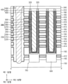
도 1 내지 도 4는 예시적인 실시예들에 따른 수직형 비휘발성 메모리 장치를 설명하기 위한 평면도들 및 단면도들이다. 구체적으로, 도 1 및 2는 평면도들이고, 도 3은 도 1의 A-A'선을 따라 절단한 단면도이며, 도 4는 도 1의 B-B'선을 따라 절단한 단면도이다. 이때, 도 2는 도 1의 X 영역에 대한 확대 평면도이다.FIGS. 1 to 4 are plan views and cross-sectional views for explaining a vertical nonvolatile memory device according to exemplary embodiments. Specifically, FIGS. 1 and 2 are plan views, FIG. 3 is a cross-sectional view taken along line A-A' of FIG. 1, and FIG. 4 is a cross-sectional view taken along line B-B' of FIG. 1. In this case, FIG. 2 is an enlarged plan view of area X of FIG. 1.
도 1 내지 도 4를 참조하면, 상기 수직형 비휘발성 메모리 장치는 제1 기판(100) 상에 형성된 기둥 구조물(700), 게이트 전극 구조물, 도전성 패드(320), 제1 및 제2 콘택 플러그들(450, 460), 및 제1 및 제2 비트 라인들(480, 490)을 포함할 수 있다. 또한, 상기 수직형 비휘발성 메모리 장치는 채널 연결 패턴(380), 지지막(150), 지지 패턴(도시되지 않음), 절연 패턴(165), 분리 구조물(435), 분리막(330), 제3 블로킹 막(400), 제1 내지 제5 층간 절연막들(180, 310, 340, 440, 470)을 더 포함할 수 있다.Referring to FIGS. 1 to 4, the vertical nonvolatile memory device may include a pillar structure (700), a gate electrode structure, a conductive pad (320), first and second contact plugs (450, 460), and first and second bit lines (480, 490) formed on a first substrate (100). In addition, the vertical nonvolatile memory device may further include a channel connection pattern (380), a support film (150), a support pattern (not shown), an insulating pattern (165), a separation structure (435), a separation film (330), a third blocking film (400), and first to fifth interlayer insulating films (180, 310, 340, 440, 470).
제1 기판(100)은 실리콘, 게르마늄, 실리콘-게르마늄과 같은 반도체 물질, 또는 GaP, GaAs, GaSb 등과 같은 Ⅲ-Ⅴ족 화합물을 포함할 수 있다. 일부 실시예들에 따르면, 제1 기판(100)은 실리콘-온-인슐레이터(SOI) 기판 또는 게르마늄-온-인슐레이터(GOI) 기판일 수 있다. The first substrate (100) may include a semiconductor material such as silicon, germanium, silicon-germanium, or a group III-V compound such as GaP, GaAs, GaSb, etc. According to some embodiments, the first substrate (100) may be a silicon-on-insulator (SOI) substrate or a germanium-on-insulator (GOI) substrate.
기둥 구조물(700)은 제1 기판(100) 상에 상기 제1 방향을 따라 교대로 배치된 게이트 전극들(412, 414, 416) 및 절연 패턴(165)을 포함하는 몰드, 및 상기 몰드 상에 형성된 제1 층간 절연막(180)을 관통하여 제1 기판(100) 상면을 노출시키는 채널 홀(190) 내에 형성될 수 있으며, 이에 따라 상기 제1 방향으로 연장될 수 있다. 기둥 구조물(700)은 채널 홀(190)의 형상에 따라, 상부에서 보았을 때, 예를 들어 원 형상을 가질 수 있으나 본 발명의 개념은 이에 한정되지는 않는다.A pillar structure (700) may be formed in a mold including gate electrodes (412, 414, 416) and an insulating pattern (165) alternately arranged along the first direction on a first substrate (100), and a channel hole (190) that penetrates a first interlayer insulating film (180) formed on the mold to expose an upper surface of the first substrate (100), thereby extending in the first direction. Depending on the shape of the channel hole (190), the pillar structure (700) may have, for example, a circular shape when viewed from above, but the concept of the present invention is not limited thereto.
채널(240), 채널(240)의 외측벽을 감싸는 제1 전하 저장 구조물(230), 채널(240)의 내측벽에 형성된 제2 전하 저장 구조물(280), 제2 전하 저장 구조물(280)의 내측벽에 형성된 제4 블로킹 막(290), 및 제4 블로킹 막(290)에 의해 저면 및 측벽이 커버되며 상기 제1 방향으로 연장되는 필라(pillar) 형상의 제4 게이트 전극(300)을 포함할 수 있다.It may include a channel (240), a first charge storage structure (230) surrounding an outer wall of the channel (240), a second charge storage structure (280) formed on an inner wall of the channel (240), a fourth blocking film (290) formed on an inner wall of the second charge storage structure (280), and a fourth gate electrode (300) in the shape of a pillar extending in the first direction and having a bottom surface and side walls covered by the fourth blocking film (290).
채널(240)은 제1 기판(100) 상에 상기 제1 방향으로 연장될 수 있으며 컵 형상을 가질 수 있다. 채널(240)은 불순물이 도핑되거나 또는 도핑되지 않은 단결정 실리콘을 포함할 수 있다.The channel (240) may extend in the first direction on the first substrate (100) and may have a cup shape. The channel (240) may include single crystal silicon that is doped with impurities or is not doped.
채널(240)은 상기 제2 및 제3 방향들을 따라 각각 복수 개로 형성되어 채널 어레이를 정의할 수 있다. 예시적인 실시예들에 있어서, 상기 채널 어레이는 상기 제2 방향을 따라 복수 개로 형성된 제1 채널들을 포함하는 제1 채널 열(240a)과, 상기 제2 방향을 따라 복수 개로 형성된 제2 채널들을 포함하면서 상기 제3 방향으로 제1 채널 열과 일정한 간격으로 이격된 제2 채널 열(240b)을 포함할 수 있다. 상기 제1 채널들은 상기 제2 채널들로부터 상기 제2 방향과 예각을 이루는 방향에 각각 위치할 수 있으며, 상기 제1 및 제2 채널들은 전체적으로 상기 제2 방향을 기준으로 지그재그 형상으로 배열될 수 있다. The channel (240) may be formed in a plurality of pieces along the second and third directions to define a channel array. In exemplary embodiments, the channel array may include a first channel row (240a) including a plurality of first channels formed along the second direction, and a second channel row (240b) including a plurality of second channels formed along the second direction and spaced apart from the first channel row by a constant interval in the third direction. The first channels may be respectively positioned in a direction forming an acute angle with respect to the second direction from the second channels, and the first and second channels may be arranged in a zigzag shape overall with respect to the second direction.
제1 및 제2 채널 열들(240a, 240b)은 상기 제3 방향을 따라 교대로 반복적으로 배열될 수 있다. 예시적인 실시예들에 있어서, 상기 제3 방향을 따라 5개의 제1 채널 열들(240a) 및 4개의 제2 채널 열들(240b)이 교대로 배치될 수 있으며, 이들은 하나의 채널 블록을 형성할 수 있다. 상기 채널 홀 어레이는 상기 제3 방향을 따라 서로 이격된 복수의 채널 블록들을 포함할 수 있다.The first and second channel rows (240a, 240b) may be alternately and repeatedly arranged along the third direction. In exemplary embodiments, five first channel rows (240a) and four second channel rows (240b) may be alternately arranged along the third direction, and these may form one channel block. The channel hole array may include a plurality of channel blocks spaced apart from each other along the third direction.
다만, 하나의 채널 블록이 포함하는 상기 채널 열들의 개수는 전술한 것에 한정되지 않을 수 있다. 이하에서는 예시적으로, 상기 채널 블록 내에 배열된 4개의 채널 열들을 상기 제3 방향을 따라 순서대로 제1, 제2, 제3 및 제4 채널 열들(240a, 240b, 240c, 240d)로 지칭하고, 가운데에 배치된 채널 열은 제5 채널 열(240e)로 지칭하며, 나머지 4개의 채널 열들을 다시 제1, 제2, 제3 및 제4 채널 열들(240a, 240b, 240c, 240d)로 지칭한다.However, the number of channel columns included in one channel block may not be limited to the above-described number. Hereinafter, by way of example, four channel columns arranged in the channel block are referred to as first, second, third, and fourth channel columns (240a, 240b, 240c, 240d) in order along the third direction, the channel column arranged in the middle is referred to as a fifth channel column (240e), and the remaining four channel columns are again referred to as first, second, third, and fourth channel columns (240a, 240b, 240c, 240d).
제1 전하 저장 구조물(230)은 채널(240)의 대부분의 외측벽을 커버하도록 상기 제1 방향으로 연장되어 실린더 형상을 갖는 상부, 및 제1 기판(100) 상에 형성되어 상기 상부와 분리되며 채널(240)의 저면 및 하부 측벽을 커버하는 컵 형상의 하부를 포함할 수 있다. 제1 전하 저장 구조물(230)의 상기 각 상부 및 하부는 채널(240)의 외측벽 및/또는 저면으로부터 순차적으로 적층된 제1 터널 절연막(220), 제1 전하 저장막(210) 및 제1 블로킹 막(200)을 포함할 수 있다.The first charge storage structure (230) may include an upper portion having a cylindrical shape that extends in the first direction to cover most of the outer wall of the channel (240), and a lower portion having a cup shape that is formed on the first substrate (100) and is separated from the upper portion and covers the bottom surface and the lower sidewall of the channel (240). Each of the upper portion and the lower portion of the first charge storage structure (230) may include a first tunnel insulating film (220), a first charge storage film (210), and a first blocking film (200) that are sequentially laminated from the outer wall and/or the bottom surface of the channel (240).
제2 전하 저장 구조물(280)은 상기 제1 방향으로 연장되어 컵 형상을 가질 수 있다. 제2 전하 저장 구조물(280)은 채널(240)의 내측벽으로부터 순차적으로 적층된 제2 터널 절연막(250), 제2 전하 저장막(260) 및 제2 블로킹 막(270)을 포함할 수 있다.The second charge storage structure (280) may extend in the first direction and have a cup shape. The second charge storage structure (280) may include a second tunnel insulating film (250), a second charge storage film (260), and a second blocking film (270) sequentially laminated from the inner wall of the channel (240).
각 제1 및 제2 터널 절연막들(220, 250)은 예를 들어, 실리콘 산화물과 같은 산화물을 포함할 수 있고, 각 제1 및 제2 전하 저장막들(210, 260)은 예를 들어, 실리콘 질화물과 같은 질화물을 포함할 수 있으며, 각 제1 및 제2 블로킹 막들(200, 270)은 예를 들어, 실리콘 산화물과 같은 산화물을 포함할 수 있다.Each of the first and second tunnel insulating films (220, 250) may include an oxide, such as, for example, silicon oxide, each of the first and second charge storage films (210, 260) may include a nitride, such as, for example, silicon nitride, and each of the first and second blocking films (200, 270) may include an oxide, such as, for example, silicon oxide.
제4 블로킹 막(290)은 상기 제1 방향으로 연장되어 컵 형상을 가질 수 있다. 제4 블로킹 막(290)은 예를 들어, 알루미늄 산화물, 하프늄 산화물 등과 같은 금속 산화물을 포함할 수 있다.The fourth blocking film (290) may extend in the first direction and have a cup shape. The fourth blocking film (290) may include a metal oxide, such as aluminum oxide or hafnium oxide, for example.
제4 게이트 전극(300)은 측벽 및 저면이 제4 블로킹 막(290)에 의해 커버될 수 있다. 제4 게이트 전극(300)은 예를 들어, 텅스텐, 구리, 알루미늄, 티타늄, 탄탈륨 등과 같은 금속을 포함할 수 있다.The fourth gate electrode (300) may have its sidewall and bottom surface covered by a fourth blocking film (290). The fourth gate electrode (300) may include a metal such as, for example, tungsten, copper, aluminum, titanium, tantalum, etc.
상기 게이트 전극 구조물은 제1 기판(100) 상에 상기 제1 방향을 따라 서로 이격되며 각각이 기둥 구조물(700)을 둘러싸는 복수의 게이트 전극들(412, 414, 416)을 포함할 수 있다. 각 게이트 전극들(412, 414, 416)은 상기 제2 방향으로 연장될 수 있고, 게이트 전극들(412, 414, 416)의 상기 제2 방향으로의 연장 길이는 하층에서 상층으로 갈수록 점차 작아질 수 있으며, 이에 따라 상기 게이트 전극 구조물은 계단 형상을 가질 수 있다. The above gate electrode structure may include a plurality of gate electrodes (412, 414, 416) spaced apart from each other along the first direction on the first substrate (100) and each surrounding a pillar structure (700). Each of the gate electrodes (412, 414, 416) may extend in the second direction, and an extension length of the gate electrodes (412, 414, 416) in the second direction may gradually decrease from a lower layer to an upper layer, and thus the gate electrode structure may have a step shape.
게이트 전극들(412, 414, 416)은 상기 제1 방향을 따라 순차적으로 적층된 제1 내지 제3 게이트 전극들(412, 414, 416)을 포함할 수 있다. 이때, 상기 제2 방향으로 연장된 제1 게이트 전극(412)은 그라운드 선택 라인(GSL) 역할을 수행할 수 있고, 상기 제2 방향으로 연장된 제2 게이트 전극(414)은 워드라인(WL) 역할을 수행할 수 있으며, 상기 제2 방향으로 연장된 제3 게이트 전극(416)은 스트링 선택 라인(SSL) 역할을 수행할 수 있다. 한편, 채널(240)의 외측벽에 형성되는 각 제1 내지 제3 게이트 전극들(412, 414, 416)은 프론트 게이트(Front Gate: FG)로, 채널(240)의 내측벽에 형성되는 제4 게이트 전극(300)은 백 게이트(Back Gate: BG)로 지칭할 수도 있다.The gate electrodes (412, 414, 416) may include first to third gate electrodes (412, 414, 416) sequentially stacked along the first direction. At this time, the first gate electrode (412) extended in the second direction may function as a ground select line (GSL), the second gate electrode (414) extended in the second direction may function as a word line (WL), and the third gate electrode (416) extended in the second direction may function as a string select line (SSL). Meanwhile, each of the first to third gate electrodes (412, 414, 416) formed on the outer wall of the channel (240) may be referred to as a front gate (FG), and the fourth gate electrode (300) formed on the inner wall of the channel (240) may be referred to as a back gate (BG).
각 제1 내지 제3 게이트 전극들(412, 414, 416)은 1개 혹은 복수 개의 층에 형성될 수 있다. 예시적인 실시예들에 있어서, 제1 게이트 전극(412)은 최하층에 형성되고, 제3 게이트 전극(416)은 최상층 및 그 하부의 1개의 층에 형성되며, 제2 게이트 전극(414)은 제1 게이트 전극(412) 및 제3 게이트 전극(416) 사이에서 복수의 층들에 형성될 수 있다. Each of the first to third gate electrodes (412, 414, 416) may be formed in one or more layers. In exemplary embodiments, the first gate electrode (412) is formed in the lowest layer, the third gate electrode (416) is formed in the uppermost layer and one layer below it, and the second gate electrode (414) may be formed in multiple layers between the first gate electrode (412) and the third gate electrode (416).
한편, 각 게이트 전극들(412, 414, 416)은 도전 패턴 및 이의 상하면 및 일부 측벽을 커버하는 배리어 패턴을 포함할 수 있다. 상기 도전 패턴은 예를 들어, 텅스텐, 티타늄, 탄탈륨, 백금 등의 전기 저항이 낮은 금속을 포함할 수 있고, 상기 배리어 패턴은 예를 들어, 티타늄 질화물, 탄탈륨 질화물 등의 금속 질화물을 포함할 수 있다. Meanwhile, each of the gate electrodes (412, 414, 416) may include a conductive pattern and a barrier pattern covering the upper and lower surfaces and some sidewalls thereof. The conductive pattern may include a metal having low electrical resistance, such as tungsten, titanium, tantalum, or platinum, and the barrier pattern may include a metal nitride, such as titanium nitride or tantalum nitride.
각 게이트 전극들(412, 414, 416)의 상면, 저면, 및 기둥 구조물(700)에 대향하는 측벽은 제3 블로킹 막(400)에 의해 커버될 수 있다. 제3 블로킹 막(400)은 예를 들어, 알루미늄 산화물, 하프늄 산화물 등의 금속 산화물을 포함할 수 있으며, 각 절연 패턴들(165), 지지막(150), 채널 연결 패턴(380), 제1 내지 제3 층간 절연막들(180, 310, 340)의 측벽도 커버할 수 있다.The upper surface, the lower surface, and the sidewall facing the pillar structure (700) of each of the gate electrodes (412, 414, 416) may be covered by a third blocking film (400). The third blocking film (400) may include, for example, a metal oxide such as aluminum oxide or hafnium oxide, and may also cover the sidewalls of each of the insulating patterns (165), the support film (150), the channel connection pattern (380), and the first to third interlayer insulating films (180, 310, 340).
상기 제1 방향으로 서로 이웃하는 게이트 전극들(412, 414, 416) 사이에는 절연 패턴(165)이 형성될 수 있으며, 게이트 전극들(412, 414, 416) 및 절연 패턴(165)은 함께 상기 제2 방향으로 배치된 계단층들을 포함하는 계단 형상의 상기 몰드를 형성할 수 있다. 절연 패턴(165)은 예를 들어, 실리콘 산화물과 같은 산화물을 포함할 수 있다. An insulating pattern (165) may be formed between the gate electrodes (412, 414, 416) adjacent to each other in the first direction, and the gate electrodes (412, 414, 416) and the insulating pattern (165) may together form the mold in a step shape including step layers arranged in the second direction. The insulating pattern (165) may include an oxide such as silicon oxide, for example.
상기 게이트 전극 구조물은 상기 제2 방향으로 연장될 수 있으며, 상기 제3 방향을 따라 복수 개로 형성될 수 있다. 이때, 상기 게이트 전극 구조물은 상기 제2 방향으로 연장되는 분리 구조물(435)에 의해 분리될 수 있다.The above gate electrode structure may extend in the second direction and may be formed in multiple pieces along the third direction. At this time, the gate electrode structure may be separated by a separation structure (435) extending in the second direction.
분리 구조물(435)은 제1 기판(100) 상에 형성되어 상기 몰드, 절연 패턴(165), 채널 연결 패턴(380), 지지막(150), 및 제1 내지 제3 층간 절연막들(180, 310, 340)을 관통하면서 상기 제2 방향으로 연장되는 공통 소스 라인(CSL)(430), 및 이의 상기 제3 방향으로의 각 양 측벽들에 형성된 제2 스페이서(420)를 포함할 수 있다. CSL(430)는 금속, 금속 질화물, 금속 실리사이드 등을 포함할 수 있으며, 제2 스페이서(420)는 예를 들어, 실리콘 산화물과 같은 산화물을 포함할 수 있다.A separation structure (435) may include a common source line (CSL) (430) formed on a first substrate (100) and extending in the second direction while penetrating the mold, the insulating pattern (165), the channel connection pattern (380), the support film (150), and the first to third interlayer insulating films (180, 310, 340), and a second spacer (420) formed on each of the sidewalls thereof in the third direction. The CSL (430) may include a metal, a metal nitride, a metal silicide, or the like, and the second spacer (420) may include an oxide, such as silicon oxide, for example.
분리막(330)은 각 채널 블록들의 상기 제3 방향으로의 가운데 부분에서 상기 제2 방향으로 연장되도록 형성될 수 있으며, 제5 채널 열(240e)에 포함된 채널들(240)의 상부를 관통할 수 있다. 이에 따라, 제5 채널 열(240e)에 포함된 채널들(240)은 실제 채널로 사용되지 않는 더미 채널들일 수 있다.The separator (330) may be formed to extend from the center portion of each channel block in the third direction in the second direction, and may penetrate the upper portion of the channels (240) included in the fifth channel row (240e). Accordingly, the channels (240) included in the fifth channel row (240e) may be dummy channels that are not used as actual channels.
예시적인 실시예들에 있어서, 분리막(330)은 채널들(240) 상부뿐만 아니라, 제1 및 제2 층간 절연막들(180, 310), 및 상부 2개 층들에 형성된 절연막들(160) 및 제3 게이트 전극들(416)을 관통할 수 있다. 이에 따라, 상기 게이트 전극 구조물에서 상부 2개의 층들에 각각 형성된 제3 게이트 전극들(416)은 분리막(330)에 의해 상기 제3 방향으로 분리될 수 있다.In exemplary embodiments, the separator (330) may penetrate not only the upper portion of the channels (240), but also the first and second interlayer insulating films (180, 310), the insulating films (160) formed in the upper two layers, and the third gate electrodes (416). Accordingly, the third gate electrodes (416) formed in each of the upper two layers of the gate electrode structure may be separated in the third direction by the separator (330).
채널 연결 패턴(380)은 제1 기판(100) 상에서 제1 게이트 전극(412) 아래에 형성되어 각 채널들(240)의 하부 외측벽, 즉 제1 전하 저장 구조물(230)의 상기 상부 및 하부 사이에 형성되어 이들에 의해 커버되지 않는 각 채널들(240)의 외측벽에 접촉할 수 있으며, 이에 따라 각 채널 블록들에 포함된 채널들(240)이 서로 연결될 수 있다. 채널 연결 패턴(380)은 예를 들어, n형 불순물이 도핑된 폴리실리콘을 포함할 수 있으며, 내부에 에어 갭(390)이 형성될 수 있다.The channel connection pattern (380) is formed below the first gate electrode (412) on the first substrate (100) and may contact the outer wall of the lower portion of each channel (240), that is, the outer wall of each channel (240) that is not covered by the upper and lower portions of the first charge storage structure (230), so that the channels (240) included in each channel block may be connected to each other. The channel connection pattern (380) may include, for example, polysilicon doped with an n-type impurity, and an air gap (390) may be formed therein.
지지막(150)은 채널 연결 패턴(380)과 제1 게이트 전극(412) 사이에 형성될 수 있다. 다만, 지지막(150)의 일부는 채널 연결 패턴(380)을 관통하여 제1 기판(100) 상면에 접촉할 수 있으며, 이 부분은 지지 패턴(도시되지 않음)으로 지칭할 수 있다. 상기 지지 패턴은 복수 개로 형성될 수 있으며, 다양한 레이아웃으로 형성될 수 있다. 즉, 상기 지지 패턴은 상기 각 제2 및 제3 방향들을 따라 서로 이격되도록 복수 개로 형성되거나, 혹은 이들 중 일부는 상기 제2 방향 혹은 제3 방향을 따라 연장될 수 있다.The support film (150) may be formed between the channel connection pattern (380) and the first gate electrode (412). However, a part of the support film (150) may penetrate the channel connection pattern (380) and contact the upper surface of the first substrate (100), and this part may be referred to as a support pattern (not shown). The support pattern may be formed in multiple pieces and may be formed in various layouts. That is, the support pattern may be formed in multiple pieces so as to be spaced apart from each other along the second and third directions, or some of them may extend along the second direction or the third direction.
예시적인 실시예들에 있어서, 도전성 패드(320)는 제2 층간 절연막(310)을 관통할 수 있으며, 상기 제1 방향을 따라 채널(240)과는 오버랩되고 제4 게이트 전극(300)과는 오버랩되지 않는 링(ring) 형상을 가질 수 있다. 예를 들어, 도전성 패드(320)는 외곽선이 타원 형상이되 내부에는 원 형상의 개구를 가질 수 있다. 이와는 달리, 도 10을 함께 참조하면, 도전성 패드(320)는 외곽선이 직사각 형상이되 내부에 원 형상의 개구를 가질 수도 있다. 도전성 패드(320)가 이와 같이 링 형상을 가짐에 따라서, 하부의 채널(240)과는 접촉하면서도, 기둥 구조물(700)과 상기 제1 방향으로 오버랩되지 않는 부분을 더 포함할 수 있다.In exemplary embodiments, the conductive pad (320) may penetrate the second interlayer insulating film (310) and may have a ring shape that overlaps the channel (240) along the first direction and does not overlap the fourth gate electrode (300). For example, the conductive pad (320) may have an oval shape as an outline and a circular opening inside. Alternatively, referring to FIG. 10, the conductive pad (320) may have a rectangular shape as an outline and a circular opening inside. Since the conductive pad (320) has a ring shape as such, it may further include a portion that is in contact with the lower channel (240) but does not overlap with the pillar structure (700) in the first direction.
도전성 패드(320)은 예를 들어, 불순물이 도핑된 단결정 실리콘을 포함할 수 있다. 도전성 패드(320)는 수 있다.The conductive pad (320) may include, for example, single crystal silicon doped with impurities. The conductive pad (320) may be.
제1 콘택 플러그(450)는 제2 내지 제4 층간 절연막들(310, 340, 440)을 관통하여 제4 게이트 전극(300) 상면에 접촉할 수 있다. 예시적인 실시예들에 있어서, 제1 콘택 플러그(450)는 제5 채널 열(240e)에 속하는 채널들(240)을 포함하는 기둥 구조물들(700)을 제외한 나머지 각 기둥 구조물들(700)에 포함된 제4 게이트 전극(300) 상면에 접촉하도록 형성될 수 있다. The first contact plug (450) may contact the upper surface of the fourth gate electrode (300) by penetrating the second to fourth interlayer insulating films (310, 340, 440). In exemplary embodiments, the first contact plug (450) may be formed to contact the upper surface of the fourth gate electrode (300) included in each of the remaining pillar structures (700) except for the pillar structures (700) including the channels (240) belonging to the fifth channel column (240e).
제2 콘택 플러그(460)는 제3 및 제4 층간 절연막들(340, 440)을 관통하여 도전성 패드(320) 상면에 접촉할 수 있다. 예시적인 실시예들에 있어서, 제2 콘택 플러그(460)는 제5 채널 열(240e)에 속하는 채널들(240)을 포함하는 기둥 구조물들(700)을 제외한 나머지 각 기둥 구조물들(700) 상에 형성된 도전성 패드(320) 상면에 접촉하도록 형성될 수 있다. 일 실시예에 있어서, 제2 콘택 플러그들(460)은 상기 제2 방향으로 연장되는 분리막(330)을 기준으로 그 양측에 대칭적으로 배치될 수 있다.The second contact plug (460) may penetrate the third and fourth interlayer insulating films (340, 440) and contact the upper surface of the conductive pad (320). In exemplary embodiments, the second contact plug (460) may be formed to contact the upper surface of the conductive pad (320) formed on each of the pillar structures (700) except for the pillar structures (700) including the channels (240) belonging to the fifth channel row (240e). In one embodiment, the second contact plugs (460) may be symmetrically arranged on both sides of the separator (330) extending in the second direction.
각 제1 및 제2 비트 라인들(480, 490)은 제5 층간 절연막(470)을 관통하면서 상기 제3 방향으로 연장될 수 있으며, 상기 제2 방향을 따라 서로 이격되도록 각각 복수 개로 형성될 수 있다. 이때, 각 제1 비트 라인들(480)은 상기 제3 방향으로 배치된 제1 콘택 플러그들(450) 상면에 공통적으로 접촉할 수 있으며, 각 제2 비트 라인들(490)은 상기 제3 방향으로 배치된 제2 콘택 플러그들(460) 상면에 공통적으로 접촉할 수 있다. Each of the first and second bit lines (480, 490) may extend in the third direction while penetrating the fifth interlayer insulating film (470), and may be formed in multiple numbers so as to be spaced apart from each other along the second direction. At this time, each of the first bit lines (480) may commonly contact the upper surface of the first contact plugs (450) arranged in the third direction, and each of the second bit lines (490) may commonly contact the upper surface of the second contact plugs (460) arranged in the third direction.
예시적인 실시예들에 있어서, 상기 제2 방향으로 서로 이웃하는 제1 비트 라인들(480) 사이에는 2개의 제2 비트 라인들(490)이 배치될 수 있다.In exemplary embodiments, two second bit lines (490) may be arranged between the first bit lines (480) adjacent to each other in the second direction.
제1 층간 절연막(180)은 상기 몰드를 커버하면서 제1 기판(100) 및 최상층 절연 패턴(165) 상에 형성될 수 있으며, 제2 내지 제5 층간 절연막들(310, 340, 440, 470)은 제1 층간 절연막(180) 상에 순차적으로 적층될 수 있다. 제1 내지 제5 층간 절연막들(180, 310, 340, 440, 470)은 예를 들어, 실리콘 산화물과 같은 산화물을 포함할 수 있으며, 이들은 서로 병합될 수도 있다.The first interlayer insulating film (180) may be formed on the first substrate (100) and the uppermost insulating pattern (165) while covering the mold, and the second to fifth interlayer insulating films (310, 340, 440, 470) may be sequentially laminated on the first interlayer insulating film (180). The first to fifth interlayer insulating films (180, 310, 340, 440, 470) may include an oxide such as silicon oxide, for example, and they may be merged with each other.
전술한 바와 같이, 상기 수직형 비휘발성 메모리 장치는 채널(240)의 외측벽 및 내측벽에 각각 제1 및 제2 전하 저장 구조물들(230, 280)이 형성될 수 있으며, 제1 전하 저장 구조물(230)은 각 제1 내지 제3 게이트 전극들(412, 414, 416)에 의해 둘러싸일 수 있고, 제2 전하 저장 구조물(280)에 인접하여 제4 게이트 전극(300)이 형성될 수 있다. As described above, the vertical non-volatile memory device may have first and second charge storage structures (230, 280) formed on the outer and inner walls of the channel (240), respectively, and the first charge storage structure (230) may be surrounded by first to third gate electrodes (412, 414, 416), respectively, and a fourth gate electrode (300) may be formed adjacent to the second charge storage structure (280).
이에 따라, 각 제2 게이트 전극들(414), 채널(240) 및 제1 전하 저장 구조물(230)에 더하여, 제4 게이트 전극(300) 및 제2 전하 저장 구조물(280)을 더 포함하는 메모리 셀들이 형성될 수 있다. 따라서, 프론트 게이트(FG) 즉, 각 제2 게이트 전극들(414)이 채널(240) 및 제1 전하 저장 구조물(230)을 통해 구현할 수 있는 문턱 전압 레벨에 더하여, 백 게이트(BG) 즉, 제4 게이트 전극(300)이 채널(240) 및 제2 전하 저장 구조물(280)을 통해 구현할 수 있는 문턱 전압 레벨이 추가적으로 확보될 수 있으므로, 상기 각 메모리 셀들은 멀티 레벨 셀의 특징을 용이하게 가질 수 있다. 상기 수직형 비휘발성 메모리 장치의 동작 방법에 대해서는 후술하기로 한다.Accordingly, in addition to each of the second gate electrodes (414), the channel (240), and the first charge storage structure (230), memory cells further including a fourth gate electrode (300) and a second charge storage structure (280) can be formed. Accordingly, in addition to the threshold voltage level that the front gate (FG), i.e., each of the second gate electrodes (414), can implement through the channel (240) and the first charge storage structure (230), a threshold voltage level that the back gate (BG), i.e., the fourth gate electrode (300), can implement through the channel (240) and the second charge storage structure (280) can be additionally secured, so that each of the memory cells can easily have the characteristics of a multi-level cell. The operating method of the vertical nonvolatile memory device will be described later.
도 5 내지 도 18은 예시적인 실시예들에 따른 수직형 비휘발성 메모리 장치의 제조 방법을 설명하기 위한 평면도들 및 단면도들이다. 구체적으로, 도 7-8, 10-12 및 17은 평면도들이고, 도 5-6, 9, 13-16 및 18은 대응하는 각 평면도들의 A-A'선을 따라 절단한 단면도들이다. 이때, 도 8 및 10은 도 7의 X 영역에 대한 확대 평면도들이다. FIGS. 5 to 18 are plan views and cross-sectional views for explaining a method of manufacturing a vertical nonvolatile memory device according to exemplary embodiments. Specifically, FIGS. 7-8, 10-12, and 17 are plan views, and FIGS. 5-6, 9, 13-16, and 18 are cross-sectional views taken along line A-A' of the corresponding plan views, respectively. At this time, FIGS. 8 and 10 are enlarged plan views for the X region of FIG. 7.
도 5를 참조하면, 제1 기판(100) 상에 희생막 구조물(140) 및 지지막(150)을 형성하고, 지지막(150) 상에 절연막(160) 및 제4 희생막(170)을 상기 제1 방향을 따라 교대로 반복적으로 적층하여 몰드막을 형성할 수 있다.Referring to FIG. 5, a sacrificial film structure (140) and a support film (150) are formed on a first substrate (100), and an insulating film (160) and a fourth sacrificial film (170) are alternately and repeatedly laminated along the first direction on the support film (150) to form a mold film.
희생막 구조물(140)은 순차적으로 적층된 제1 내지 제3 희생막들(110, 120, 130)을 포함할 수 있다. 이때, 각 제1 및 제3 희생막들(110, 130)은 예를 들어, 실리콘 산화물과 같은 산화물을 포함할 수 있고, 제2 희생막(120)은 예를 들어, 실리콘 질화물과 같은 질화물을 포함할 수 있다. The sacrificial film structure (140) may include first to third sacrificial films (110, 120, 130) that are sequentially stacked. At this time, each of the first and third sacrificial films (110, 130) may include an oxide, such as silicon oxide, for example, and the second sacrificial film (120) may include a nitride, such as silicon nitride, for example.
지지막(150)은 제1 내지 제3 희생막들(110, 120, 130)에 대해 식각 선택비를 갖는 물질, 예를 들어, n형의 불순물이 도핑된 폴리실리콘을 포함할 수 있다. The support film (150) may include a material having an etching selectivity with respect to the first to third sacrificial films (110, 120, 130), for example, polysilicon doped with n-type impurities.
한편 도시하지는 않았으나, 절연막(160)을 형성하기 이전에 희생막 구조물(140)을 부분적으로 제거하여 제1 기판(100)의 상면을 노출시키는 제1 개구(도시하지 않음)를 형성한 후, 지지막(150)이 상기 제1 개구를 적어도 부분적으로 채우도록 제1 기판(100) 및 희생막 구조물(140) 상에 형성될 수도 있으며, 이에 따라 상기 제1 개구 내에 지지 패턴(도시되지 않음)이 형성될 수 있다. Meanwhile, although not illustrated, before forming the insulating film (160), a first opening (not illustrated) is formed by partially removing the sacrificial film structure (140) to expose the upper surface of the first substrate (100), and then a support film (150) may be formed on the first substrate (100) and the sacrificial film structure (140) to at least partially fill the first opening, so that a support pattern (not illustrated) may be formed within the first opening.
절연막(160)은 예를 들어, 실리콘 산화물과 같은 산화물을 포함할 수 있으며, 제4 희생막(170)은 절연막(160)에 대해 높은 식각 선택비를 갖는 물질, 예를 들어 실리콘 질화물과 같은 질화물을 포함할 수 있다.The insulating film (160) may include an oxide, such as silicon oxide, for example, and the fourth sacrificial film (170) may include a material having a high etching selectivity with respect to the insulating film (160), for example, a nitride, such as silicon nitride.
도 6을 참조하면, 최상층에 형성된 절연막(160)을 부분적으로 커버하는 포토레지스트 패턴(도시되지 않음)을 최상층 절연막(160) 상에 형성한 후, 이를 식각 마스크로 사용하여 최상층 절연막(160) 및 그 하부의 최상층 제4 희생막(170)을 식각한다. 이에 따라, 최상층 제4 희생막(170) 하부에 형성된 절연막(160)의 일부가 노출될 수 있다. 상기 포토레지스트 패턴의 면적을 일정한 비율로 축소시키는 트리밍 공정을 수행한 후, 이를 식각 마스크로 사용하여 최상층 절연막(160), 최상층 제4 희생막(170), 상기 노출된 절연막(160), 및 그 하부의 제4 희생막(170)을 다시 식각할 수 있다. Referring to FIG. 6, a photoresist pattern (not shown) partially covering an insulating film (160) formed on the uppermost layer is formed on the uppermost insulating film (160), and then the uppermost insulating film (160) and the uppermost fourth sacrificial film (170) underneath are etched using this as an etching mask. Accordingly, a part of the insulating film (160) formed underneath the uppermost fourth sacrificial film (170) may be exposed. After performing a trimming process that reduces the area of the photoresist pattern at a constant ratio, the uppermost insulating film (160), the uppermost fourth sacrificial film (170), the exposed insulating film (160), and the lower fourth sacrificial film (170) may be etched again using this as an etching mask.
상기 트리밍 공정 및 상기 식각 공정을 반복적으로 수행함으로써, 순차적으로 적층된 하나의 제4 희생막(170) 및 하나의 절연막(160)으로 각각 구성되는 복수 개의 계단층들을 포함하는 계단 구조물 형상의 몰드가 제1 기판(100) 상에 형성될 수 있다. By repeatedly performing the above trimming process and the above etching process, a mold in the shape of a step structure including a plurality of step layers each composed of one fourth sacrificial film (170) and one insulating film (160) sequentially laminated can be formed on the first substrate (100).
상기 몰드를 커버하는 제1 층간 절연막(180)을 제1 기판(100) 상에 형성하고 이를 평탄화한 후, 제1 층간 절연막(180) 및 상기 몰드를 관통하는 기둥 구조물(700)을 제1 기판(100) 상에 형성할 수 있다. 기둥 구조물(700)은 예를 들어 다음과 같이 형성될 수 있다.A first interlayer insulating film (180) covering the mold is formed on a first substrate (100) and flattened, and then a pillar structure (700) penetrating the first interlayer insulating film (180) and the mold can be formed on the first substrate (100). The pillar structure (700) can be formed, for example, as follows.
제1 층간 절연막(180) 및 상기 몰드를 건식 식각 공정을 통해 식각하여 제1 기판(100) 상면을 노출시키는 채널 홀(190)을 형성하고, 채널 홀(190)의 측벽, 상기 노출된 제1 기판(100) 상면, 및 제1 층간 절연막(180) 상면에 제1 전하 저장 구조물(230), 채널(240), 제2 전하 저장 구조물(280) 및 제4 블로킹 막(290)을 순차적으로 적층하며, 채널 홀(190)의 나머지 부분을 채우는 제4 게이트 전극(300)을 제4 블로킹 막(290) 상에 형성한 후, 제1 층간 절연막(180)의 상면이 노출될 때까지 이들을 평탄화함으로써, 채널 홀(190) 내에 기둥 구조물(700)을 형성할 수 있다. A channel hole (190) is formed by etching the first interlayer insulating film (180) and the mold through a dry etching process to expose the upper surface of the first substrate (100), and a first charge storage structure (230), a channel (240), a second charge storage structure (280), and a fourth blocking film (290) are sequentially laminated on the sidewalls of the channel hole (190), the exposed upper surface of the first substrate (100), and the upper surface of the first interlayer insulating film (180), and a fourth gate electrode (300) that fills the remaining portion of the channel hole (190) is formed on the fourth blocking film (290), and then these are flattened until the upper surface of the first interlayer insulating film (180) is exposed, thereby forming a pillar structure (700) within the channel hole (190).
예시적인 실시예들에 있어서, 상기 건식 식각 공정은 채널 홀(190)이 제1 기판(100)의 상면을 노출시킬 때까지 수행될 수 있으며, 나아가 채널 홀(190)은 제1 기판(100)의 상부 일부까지 관통하도록 형성될 수 있다. 채널 홀(190)은 상기 제2 및 제3 방향들을 따라 각각 복수 개로 형성될 수 있으며, 이에 따라 채널 홀 어레이가 정의될 수 있다. In exemplary embodiments, the dry etching process may be performed until the channel hole (190) exposes the upper surface of the first substrate (100), and further, the channel hole (190) may be formed to penetrate through an upper portion of the first substrate (100). The channel hole (190) may be formed in multiple numbers along each of the second and third directions, and thus, a channel hole array may be defined.
예시적인 실시예들에 있어서, 제1 전하 저장 구조물(230)은 채널 홀(190) 측벽 및 상기 노출된 제1 기판(100) 상면으로부터 순차적으로 적층된 제1 블로킹 막(200), 제1 전하 저장막(210), 및 제1 터널 절연막(220)을 포함할 수 있으며, 채널(240)의 외측벽에 접촉할 수 있다. 또한, 제2 전하 저장 구조물(280)은 채널(240)의 내측벽으로부터 순차적으로 적층된 제2 터널 절연막(250), 제2 전하 저장막(260), 및 제2 블로킹 막(270)을 포함할 수 있으며, 제4 블로킹 막(290)의 외측벽에 접촉할 수 있다. 제4 블로킹 막(290)은 제4 게이트 전극(300)의 측벽 및 저면을 커버할 수 있다.In exemplary embodiments, the first charge storage structure (230) may include a first blocking film (200), a first charge storage film (210), and a first tunnel insulating film (220) sequentially stacked from a sidewall of the channel hole (190) and an upper surface of the exposed first substrate (100), and may contact an outer wall of the channel (240). In addition, the second charge storage structure (280) may include a second tunnel insulating film (250), a second charge storage film (260), and a second blocking film (270) sequentially stacked from an inner wall of the channel (240), and may contact an outer wall of the fourth blocking film (290). The fourth blocking film (290) may cover a sidewall and a bottom surface of the fourth gate electrode (300).
도 7 내지 도 9를 참조하면, 제1 층간 절연막(180) 및 기둥 구조물(700) 상에 제2 층간 절연막(310)을 형성한 후, 이를 관통하면서 기둥 구조물(700)에 부분적으로 접촉하는 도전성 패드(320)를 형성할 수 있다.Referring to FIGS. 7 to 9, after forming a second interlayer insulating film (310) on a first interlayer insulating film (180) and a pillar structure (700), a conductive pad (320) that penetrates the first interlayer insulating film (180) and partially contacts the pillar structure (700) can be formed.
예시적인 실시예들에 있어서, 도전성 패드(320)는 상기 제1 방향을 따라 채널(240)과는 오버랩되고 제4 게이트 전극(300)과는 오버랩되지 않는 링(ring) 형상을 가질 수 있다. 예를 들어, 도전성 패드(320)는 외곽선이 타원 형상이되 내부에는 원 형상의 개구를 가질 수 있다. 이와는 달리, 도 10을 참조하면, 도전성 패드(320)는 외곽선이 직사각 형상이되 내부에 원 형상의 개구를 가질 수도 있다. In exemplary embodiments, the conductive pad (320) may have a ring shape that overlaps the channel (240) along the first direction and does not overlap the fourth gate electrode (300). For example, the conductive pad (320) may have an oval shape as an outer line and a circular opening inside. Alternatively, referring to FIG. 10, the conductive pad (320) may have a rectangular shape as an outer line and a circular opening inside.
도 11을 참조하면, 제1 및 제2 층간 절연막들(180, 310), 절연막(160) 및 제4 희생막(170)의 일부를 관통하는 분리막(330)을 형성할 수 있다.Referring to FIG. 11, a separation film (330) penetrating through a portion of the first and second interlayer insulating films (180, 310), the insulating film (160), and the fourth sacrificial film (170) can be formed.
분리막(330)은 건식 식각 공정을 통해 제1 및 제2 층간 절연막들(180, 310), 절연막(160) 및 제4 희생막(170), 도전성 패드(320) 및 기둥 구조물(700)의 일부를 식각함으로써, 이들을 관통하는 제1 리세스(도시하지 않음)를 형성한 후, 이를 채우도록 형성될 수 있다. The separator (330) can be formed by etching the first and second interlayer insulating films (180, 310), the insulating film (160), the fourth sacrificial film (170), the conductive pad (320), and a portion of the pillar structure (700) through a dry etching process to form a first recess (not shown) penetrating them, and then filling the recess.
도 12 및 13을 참조하면, 제2 층간 절연막(310), 도전성 패드(320) 및 분리막(330) 상에 제3 층간 절연막(340)을 형성한 후, 건식 식각 공정을 통해 제1 내지 제3 층간 절연막들(180, 310, 340) 및 상기 몰드를 관통하는 제2 개구(350)를 제1 기판(100) 상에 형성할 수 있다.Referring to FIGS. 12 and 13, after forming a third interlayer insulating film (340) on the second interlayer insulating film (310), the conductive pad (320), and the separator (330), the first to third interlayer insulating films (180, 310, 340) and the second opening (350) penetrating the mold can be formed on the first substrate (100) through a dry etching process.
상기 건식 식각 공정은 제2 개구(350)가 지지막(150) 혹은 상기 지지 패턴의 상면을 노출시킬 때까지 수행될 수 있으며, 나아가 이들의 상부 일부까지 관통하도록 형성될 수 있다. 제2 개구(350)가 형성됨에 따라서, 이의 측벽에 의해 상기 몰드에 포함된 절연막(160) 및 제4 희생막(170)이 노출될 수 있다.The above dry etching process can be performed until the second opening (350) exposes the upper surface of the support film (150) or the support pattern, and can be formed to penetrate even a portion of the upper portion thereof. As the second opening (350) is formed, the insulating film (160) and the fourth sacrificial film (170) included in the mold can be exposed by the sidewall thereof.
예시적인 실시예들에 있어서, 제2 개구(350)는 제1 기판(100) 상에서 상기 제2 방향으로 연장될 수 있으며, 상기 제3 방향을 따라 복수 개로 형성될 수 있다. 제2 개구(350)가 형성됨에 따라서, 절연막(160)은 상기 제2 방향으로 연장되는 절연 패턴(165)으로 변환될 수 있으며, 제4 희생막(170)은 상기 제2 방향으로 연장되는 제4 희생 패턴(175)으로 변환될 수 있다.In exemplary embodiments, the second opening (350) may extend in the second direction on the first substrate (100) and may be formed in multiple numbers along the third direction. As the second opening (350) is formed, the insulating film (160) may be converted into an insulating pattern (165) extending in the second direction, and the fourth sacrificial film (170) may be converted into a fourth sacrificial pattern (175) extending in the second direction.
이후, 제2 개구(350)의 측벽 및 제3 층간 절연막(340) 상에 제1 스페이서 막을 형성한 후, 이방성 식각 공정을 통해 제2 개구(350)의 저면에 형성된 부분을 제거하여 제1 스페이서(360)를 형성할 수 있으며, 이에 따라 지지막(150) 및 상기 지지 패턴 상면이 부분적으로 노출될 수 있다. Thereafter, a first spacer film is formed on the sidewall of the second opening (350) and the third interlayer insulating film (340), and then a portion formed on the bottom surface of the second opening (350) is removed through an anisotropic etching process to form a first spacer (360), whereby the support film (150) and the upper surface of the support pattern can be partially exposed.
이후, 상기 노출된 지지막(150) 및 상기 지지 패턴 부분 및 그 하부의 희생막 구조물(140) 부분을 제거함으로써, 제2 개구(350)를 하부로 확장할 수 있다. 이에 따라, 제2 개구(350)는 제1 기판(100)의 상면을 노출시킬 수 있으며, 나아가 제1 기판(100)의 상부 일부까지도 관통할 수 있다. Thereafter, the second opening (350) can be expanded downward by removing the exposed support film (150) and the support pattern portion and the sacrificial film structure (140) portion thereunder. Accordingly, the second opening (350) can expose the upper surface of the first substrate (100) and, further, can penetrate even a portion of the upper portion of the first substrate (100).
예시적인 실시예들에 있어서, 제1 스페이서(360)는 예를 들어, 불순물이 도핑되지 않은 폴리실리콘을 포함할 수 있다. In exemplary embodiments, the first spacer (360) may include, for example, undoped polysilicon.
희생막 구조물(140)이 부분적으로 제거될 때, 제2 개구(350)의 측벽은 제1 스페이서(360)에 의해 커버되므로, 상기 몰드에 포함된 절연 패턴(165) 및 제4 희생 패턴(175)은 제거되지 않을 수 있다.When the sacrificial membrane structure (140) is partially removed, the side wall of the second opening (350) is covered by the first spacer (360), so the insulating pattern (165) and the fourth sacrificial pattern (175) included in the mold may not be removed.
도 14를 참조하면, 제2 개구(350)를 통해 희생막 구조물(140)을 예를 들어, 습식 식각 공정을 통해 제거할 수 있으며, 이에 따라 제1 갭(370)이 형성될 수 있다. Referring to FIG. 14, the sacrificial film structure (140) can be removed through the second opening (350) by, for example, a wet etching process, thereby forming a first gap (370).
희생막 구조물(140)이 제거될 때, 이에 인접한 제1 전하 저장 구조물(230) 부분도 함께 제거될 수 있으며, 이에 따라 채널(240)의 외측벽 일부가 노출될 수 있다. 상기 습식 식각 공정은 예를 들어, 불산(HF) 및/또는 인산(H3PO4)을 사용하여 수행될 수 있다. 제1 갭(370)이 형성됨에 따라서, 제1 전하 저장 구조물(230)은 제1 기판(100) 상에 형성된 하부, 및 이와 상기 제1 방향으로 이격되면서 상기 몰드 내에 형성된 상부로 분리될 수 있다.When the sacrificial film structure (140) is removed, a portion of the first charge storage structure (230) adjacent thereto may also be removed, thereby exposing a portion of the outer wall of the channel (240). The wet etching process may be performed using, for example, hydrofluoric acid (HF) and/or phosphoric acid (H 3 PO 4 ). As the first gap (370) is formed, the first charge storage structure (230) may be separated into a lower portion formed on the first substrate (100) and an upper portion formed within the mold while being spaced apart from the lower portion in the first direction.
한편, 상기 습식 식각 공정을 통해 제1 갭(370)이 형성될 때, 지지막(150) 및 상기 지지 패턴은 제거되지 않을 수 있으며, 이에 따라 상기 몰드는 무너지지 않을 수 있다. Meanwhile, when the first gap (370) is formed through the wet etching process, the support film (150) and the support pattern may not be removed, and thus, the mold may not collapse.
도 15를 참조하면, 제1 스페이서(360)를 제거하고, 제2 개구(350)의 측벽 및 제1 갭(370) 내에 채널 연결층을 형성할 수 있으며, 이후 예를 들어, 에치 백 공정을 수행하여 제2 개구(350) 내에 형성된 상기 채널 연결층 부분을 제거함으로써 제1 갭(370) 내에 채널 연결 패턴(380)을 형성할 수 있다.Referring to FIG. 15, the first spacer (360) can be removed, and a channel connection layer can be formed on the sidewall of the second opening (350) and within the first gap (370), and then, for example, an etch back process can be performed to remove a portion of the channel connection layer formed within the second opening (350), thereby forming a channel connection pattern (380) within the first gap (370).
채널 연결 패턴(380)이 형성됨에 따라서, 상기 채널 어레이를 형성하는 채널들(240)이 서로 연결될 수 있다. 채널 연결 패턴(380) 내에는 에어 갭(390)이 형성될 수 있다. As the channel connection pattern (380) is formed, the channels (240) forming the channel array can be connected to each other. An air gap (390) can be formed within the channel connection pattern (380).
도 16을 참조하면, 제2 개구(350)에 의해 노출된 제4 희생 패턴들(175)을 제거하여, 각 층에 형성된 절연 패턴들(165) 사이에 제2 갭을 형성할 수 있으며, 상기 제2 갭에 의해서 제1 블로킹 막(200)의 외측벽 일부가 노출될 수 있다.Referring to FIG. 16, by removing the fourth sacrificial patterns (175) exposed by the second opening (350), a second gap can be formed between the insulating patterns (165) formed in each layer, and a part of the outer wall of the first blocking film (200) can be exposed by the second gap.
예시적인 실시예들에 따르면, 인산(H3PO4) 혹은 황산(H2SO4)을 사용하는 습식 식각 공정을 통해 제4 희생 패턴들(175)을 제거할 수 있다.According to exemplary embodiments, the fourth sacrificial patterns (175) can be removed through a wet etching process using phosphoric acid (H 3 PO 4 ) or sulfuric acid (H 2 SO 4 ).
이후, 노출된 제1 블로킹 막(200)의 외측벽, 상기 제2 갭들의 내벽, 절연 패턴들(165)의 표면, 지지막(150)의 측벽 및 일부 저면, 상기 지지 패턴의 측벽, 채널 연결 패턴(380)의 측벽, 제1 기판(100)의 상면, 및 제3 층간 절연막(340)의 상면에 제3 블로킹 막(400)을 형성하고, 제3 블로킹 막(400) 상에 게이트 전극막을 형성할 수 있다.Thereafter, a third blocking film (400) can be formed on the outer wall of the exposed first blocking film (200), the inner wall of the second gaps, the surface of the insulating patterns (165), the side wall and a portion of the bottom surface of the support film (150), the side wall of the support pattern, the side wall of the channel connection pattern (380), the upper surface of the first substrate (100), and the upper surface of the third interlayer insulating film (340), and a gate electrode film can be formed on the third blocking film (400).
상기 게이트 전극막은 순차적으로 적층된 게이트 배리어 막 및 게이트 도전막을 포함할 수 있다. The above gate electrode film may include a gate barrier film and a gate conductive film that are sequentially laminated.
이후, 상기 게이트 전극막을 부분적으로 제거함으로써, 상기 각 제2 갭들 내부에 게이트 전극을 형성할 수 있다. 예시적인 실시예들에 따르면, 상기 게이트 전극막은 습식 식각 공정을 통해 부분적으로 제거될 수 있다. Thereafter, by partially removing the gate electrode film, a gate electrode can be formed inside each of the second gaps. According to exemplary embodiments, the gate electrode film can be partially removed through a wet etching process.
예시적인 실시예들에 있어서, 상기 게이트 전극은 상기 제2 방향으로 연장될 수 있으며, 상기 제1 방향을 따라 서로 이격되도록 복수 개의 층들에 적층될 수 있다. 또한 상기 게이트 전극은 상기 제3 방향을 따라 복수 개로 형성될 수 있다. 즉, 동일한 층에 형성된 상기 복수 개의 게이트 전극들은 제2 개구(350)에 의해 상기 제3 방향으로 서로 이격될 수 있다. 상기 게이트 전극은 상기 제1 방향을 따라 순차적으로 형성된 제1 내지 제3 게이트 전극들(412, 414, 416)을 포함할 수 있다. In exemplary embodiments, the gate electrode may extend in the second direction and may be laminated in a plurality of layers spaced apart from each other along the first direction. In addition, the gate electrode may be formed in a plurality of layers along the third direction. That is, the plurality of gate electrodes formed in the same layer may be spaced apart from each other in the third direction by the second opening (350). The gate electrode may include first to third gate electrodes (412, 414, 416) sequentially formed along the first direction.
이후, 제2 개구(350)의 측벽에 제2 스페이서(420)를 형성하고, 제2 개구(350)의 나머지 부분을 채우는 공통 소스 라인(CSL)(430)을 형성할 수 있다.Thereafter, a second spacer (420) can be formed on the side wall of the second opening (350), and a common source line (CSL) (430) can be formed to fill the remaining portion of the second opening (350).
예시적인 실시예들에 있어서, CSL(430)은 상기 제2 방향으로 연장될 수 있으며, 그 측벽에 형성된 제2 스페이서(420)와 함께 각 제1 내지 제3 게이트 전극들(412, 414, 416)을 상기 제3 방향으로 분리시키는 분리 구조물(435)을 형성할 수 있다. In exemplary embodiments, the CSL (430) may extend in the second direction and, together with the second spacer (420) formed on its sidewall, form a separation structure (435) that separates each of the first to third gate electrodes (412, 414, 416) in the third direction.
도 17 및 18을 참조하면, 제3 층간 절연막(340) 및 CSL(430) 상에 제4 층간 절연막(440)을 형성한 후, 제2 내지 제4 층간 절연막들(310, 340, 440)을 관통하여 제4 게이트 전극(300) 상면에 접촉하는 제1 콘택 플러그(450), 및 제3 및 제4 층간 절연막들(340, 440)을 관통하여 도전성 패드(320) 상면에 접촉하는 제2 콘택 플러그(460)를 형성할 수 있다. Referring to FIGS. 17 and 18, after forming a fourth interlayer insulating film (440) on the third interlayer insulating film (340) and the CSL (430), a first contact plug (450) that penetrates the second to fourth interlayer insulating films (310, 340, 440) and contacts the upper surface of the fourth gate electrode (300), and a second contact plug (460) that penetrates the third and fourth interlayer insulating films (340, 440) and contacts the upper surface of the conductive pad (320) can be formed.
다시 도 1 내지 도 4를 참조하면, 제4 층간 절연막(440) 상에 제5 층간 절연막(470)을 형성한 후, 이를 관통하면서 제1 및 제2 콘택 플러그들(450, 460) 상면에 각각 접촉하는 제1 및 제2 비트 라인들(480, 490)을 형성함으로써 상기 수직형 비휘발성 메모리 장치를 완성할 수 있다.Referring again to FIGS. 1 to 4, the vertical nonvolatile memory device can be completed by forming a fifth interlayer insulating film (470) on a fourth interlayer insulating film (440), and then forming first and second bit lines (480, 490) penetrating through the fourth interlayer insulating film and contacting the upper surfaces of the first and second contact plugs (450, 460), respectively.
전술한 바와 같이, 각 기둥 구조물(700)의 채널(240)이 형성하는 내부 공간을 예를 들어, 충전 패턴으로 채우는 대신에, 제2 전하 저장 구조물(280), 제4 블로킹 막(290) 및 제4 게이트 전극(300)으로 채울 수 있으며, 이에 따라 각 제1 내지 제3 게이트 전극들(412, 414, 416)과 채널(240)을 공통적으로 사용하는 제4 게이트 전극(300)을 간단하게 형성할 수 있다.As described above, instead of filling the internal space formed by the channel (240) of each pillar structure (700) with, for example, a charging pattern, it can be filled with the second charge storage structure (280), the fourth blocking film (290), and the fourth gate electrode (300), and thus the fourth gate electrode (300) that commonly uses the channel (240) with each of the first to third gate electrodes (412, 414, 416) can be simply formed.
도 19는 예시적인 실시예들에 따른 수직형 비휘발성 메모리 장치를 설명하기 위한 단면도이다. 상기 수직형 비휘발성 메모리 장치는 일부 구성 요소들을 제외하고는, 도 1 내지 도 4에 도시된 수직형 비휘발성 메모리 장치와 실질적으로 동일하거나 유사하므로, 이들에 대한 중복적인 설명은 생략한다.FIG. 19 is a cross-sectional view illustrating a vertical nonvolatile memory device according to exemplary embodiments. The vertical nonvolatile memory device is substantially the same as or similar to the vertical nonvolatile memory devices illustrated in FIGS. 1 to 4, except for some components, and therefore, a redundant description thereof is omitted.
도 19를 참조하면, 기둥 구조물(700)은 제4 블로킹 막(290, 도 3 참조)을 포함하지 않을 수 있으며, 이에 따라 채널 홀(190)의 측벽 및 제1 기판(100) 상면으로부터 순차적으로 적층된 제1 전하 저장 구조물(230), 채널(240), 제2 전하 저장 구조물(280), 및 제4 게이트 전극(300)을 포함할 수 있다. 이때, 제4 게이트 전극(300)은 금속 대신에 n형 혹은 p형 불순물이 도핑된 폴리실리콘을 포함할 수 있다.Referring to FIG. 19, the pillar structure (700) may not include the fourth blocking film (290, see FIG. 3), and thus may include a first charge storage structure (230), a channel (240), a second charge storage structure (280), and a fourth gate electrode (300) sequentially stacked from the sidewall of the channel hole (190) and the upper surface of the first substrate (100). In this case, the fourth gate electrode (300) may include polysilicon doped with an n-type or p-type impurity instead of a metal.
도 20은 예시적인 실시예들에 따른 수직형 비휘발성 메모리 장치를 설명하기 위한 단면도이다. 상기 수직형 비휘발성 메모리 장치는 일부 구성 요소들을 제외하고는, 도 1 내지 도 4에 도시된 수직형 비휘발성 메모리 장치와 실질적으로 동일하거나 유사하므로, 이들에 대한 중복적인 설명은 생략한다.FIG. 20 is a cross-sectional view illustrating a vertical nonvolatile memory device according to exemplary embodiments. The vertical nonvolatile memory device is substantially the same as or similar to the vertical nonvolatile memory devices illustrated in FIGS. 1 to 4, except for some components, and therefore, a redundant description thereof is omitted.
도 20을 참조하면, 기둥 구조물(700)은 제1 기판(100) 상면에 접촉하는 반도체 패턴(500)을 더 포함할 수 있으며, 채널 연결 패턴(380), 지지막(150) 및 상기 지지 패턴은 형성되지 않을 수 있다.Referring to FIG. 20, the pillar structure (700) may further include a semiconductor pattern (500) that contacts the upper surface of the first substrate (100), and the channel connection pattern (380), the support film (150), and the support pattern may not be formed.
반도체 패턴(500)은 제1 기판(100)의 상부도 부분적으로 관통할 수 있으며, 최하층 절연 패턴(165) 및 제1 게이트 전극(412)을 관통할 수 있다. 예시적인 실시예들에 있어서, 반도체 패턴(500)은 그 상면의 높이가 제1 기판(100) 상면으로부터 2번째 층에 형성된 절연 패턴(165)의 하면의 높이보다 높고 상면의 높이보다 낮을 수 있다. 반도체 패턴(500)은 예를 들어, 결정질 실리콘과 같은 결정질 반도체 물질을 포함할 수 있다.The semiconductor pattern (500) may partially penetrate the upper portion of the first substrate (100) and may penetrate the lowermost insulating pattern (165) and the first gate electrode (412). In exemplary embodiments, the semiconductor pattern (500) may have a height of an upper surface thereof that is higher than the height of a lower surface of an insulating pattern (165) formed in the second layer from the upper surface of the first substrate (100) and lower than the height of an upper surface thereof. The semiconductor pattern (500) may include, for example, a crystalline semiconductor material such as crystalline silicon.
한편, 기둥 구조물(700)에 포함된 제1 전하 저장 구조물(230)은 반도체 패턴(500)의 상면 및 채널 홀(190)의 측벽 상에 형성되어 저면 중앙부가 뚫린 컵 형상을 가질 수 있으며, 채널(240)은 반도체 패턴(500)의 상면에 접촉할 수 있다.Meanwhile, the first charge storage structure (230) included in the pillar structure (700) may be formed on the upper surface of the semiconductor pattern (500) and the sidewall of the channel hole (190) and may have a cup shape with a central portion of the lower surface open, and the channel (240) may be in contact with the upper surface of the semiconductor pattern (500).
도 21 내지 도 23은 예시적인 실시예들에 따른 수직형 비휘발성 메모리 장치의 제조 방법을 설명하기 위한 단면도들이다. 상기 수직형 비휘발성 메모리 장치의 제조 방법은 도 5 내지 도 18, 및 도 1 내지 도 4를 참조로 설명한 공정들과 실질적으로 동일하거나 유사한 공정들을 포함하므로, 이들에 대한 중복적인 설명은 생략한다.FIGS. 21 to 23 are cross-sectional views illustrating a method for manufacturing a vertical nonvolatile memory device according to exemplary embodiments. The method for manufacturing the vertical nonvolatile memory device includes processes substantially the same as or similar to the processes described with reference to FIGS. 5 to 18 and FIGS. 1 to 4, and therefore, a redundant description thereof will be omitted.
도 21을 참조하면, 도 5를 참조로 설명한 공정들과 실질적으로 동일하거나 유사한 공정들을 수행한다. 다만, 희생막 구조물(140) 및 지지막(150)은 형성하지 않을 수 있으며, 이에 따라 제1 기판(100) 상에 절연막(160) 및 제4 희생막(170)이 교대로 반복적으로 적층되어 몰드막을 형성할 수 있다.Referring to FIG. 21, processes substantially the same as or similar to the processes described with reference to FIG. 5 are performed. However, the sacrificial film structure (140) and the support film (150) may not be formed, and accordingly, an insulating film (160) and a fourth sacrificial film (170) may be alternately and repeatedly laminated on the first substrate (100) to form a mold film.
도 22를 참조하면, 도 6을 참조로 설명한 공정들과 실질적으로 동일하거나 유사한 공정들을 수행한다. 다만, 몰드를 관통하는 채널 홀(190)에 의해 노출된 제1 기판(100) 상면에 반도체 패턴(500)을 추가적으로 형성할 수 있으며, 반도체 패턴(500) 상에 나머지 막 구조물들을 형성함으로써 기둥 구조물(700)을 형성할 수 있다.Referring to FIG. 22, processes substantially the same as or similar to the processes described with reference to FIG. 6 are performed. However, a semiconductor pattern (500) may be additionally formed on the upper surface of the first substrate (100) exposed by the channel hole (190) penetrating the mold, and a pillar structure (700) may be formed by forming the remaining film structures on the semiconductor pattern (500).
반도체 패턴(500)은 제1 기판(100) 상면을 씨드로 사용하는 선택적 에피택시얼 성장(SEG) 공정을 통해 형성될 수 있다.The semiconductor pattern (500) can be formed through a selective epitaxial growth (SEG) process using the upper surface of the first substrate (100) as a seed.
이후, 채널 홀(190)의 측벽, 반도체 패턴(500)의 상면, 및 제1 층간 절연막(180)의 상면에 제1 전하 저장 구조물(230) 및 제3 스페이서 막(도시되지 않음)을 순차적으로 형성하고, 상기 제3 스페이서 막을 이방성 식각하여 채널 홀(190)의 측벽에만 잔류하는 제3 스페이서(도시되지 않음)를 형성한 후, 상기 제3 스페이서를 식각 마스크로 사용하여 제1 전하 저장 구조물(230)을 식각함으로써, 반도체 패턴(500)의 상면 및 채널 홀(190)의 측벽 상에 형성되어 저면 중앙부가 뚫린 컵 형상을 갖도록 할 수 있으며, 이때 반도체 패턴(500)의 상부도 부분적으로 함께 제거될 수 있다. Thereafter, a first charge storage structure (230) and a third spacer film (not shown) are sequentially formed on the sidewall of the channel hole (190), the upper surface of the semiconductor pattern (500), and the upper surface of the first interlayer insulating film (180), and the third spacer film is anisotropically etched to form a third spacer (not shown) remaining only on the sidewall of the channel hole (190), and then the first charge storage structure (230) is etched using the third spacer as an etching mask, so that a cup shape with a central portion of the lower surface being open can be formed on the upper surface of the semiconductor pattern (500) and the sidewall of the channel hole (190). At this time, the upper portion of the semiconductor pattern (500) can also be partially removed together.
상기 제3 스페이서를 제거한 후, 노출된 반도체 패턴(500), 제1 전하 저장막 구조물(230), 및 제1 층간 절연막(180) 상에 채널(240), 제2 전하 저장 구조물(280), 제4 블로킹 막(290) 및 제4 게이트 전극(300)을 순차적으로 적층하고, 제1 층간 절연막(180) 상면이 노출될 때까지 이들을 평탄화함으로써 기둥 구조물(700)을 형성할 수 있다. 이에 따라, 채널(240)은 반도체 패턴(500) 상면에 접촉할 수 있다.After removing the third spacer, a channel (240), a second charge storage structure (280), a fourth blocking film (290), and a fourth gate electrode (300) are sequentially stacked on the exposed semiconductor pattern (500), the first charge storage film structure (230), and the first interlayer insulating film (180), and then planarized until the upper surface of the first interlayer insulating film (180) is exposed, thereby forming a pillar structure (700). Accordingly, the channel (240) can contact the upper surface of the semiconductor pattern (500).
도 23을 참조하면, 도 6 내지 도 13을 참조로 설명한 공정들과 실질적으로 동일하거나 유사한 공정들을 수행한다. 다만, 제2 개구(350)는 상기 몰드를 관통하여 제1 기판(100) 상면을 노출시킬 수 있으며, 제1 스페이서(360)는 형성되지 않을 수 있다.Referring to FIG. 23, processes substantially the same as or similar to the processes described with reference to FIGS. 6 to 13 are performed. However, the second opening (350) may penetrate the mold to expose the upper surface of the first substrate (100), and the first spacer (360) may not be formed.
이후, 도 16 내지 도 18을 참조로 설명한 공정들과 실질적으로 동일하거나 유사한 공정들을 수행함으로써, 제1 내지 제3 게이트 전극들(412, 414, 416), 제3 블로킹 막(400), 제2 스페이서(420) 및 CSL(430)를 형성할 수 있다.Thereafter, by performing processes substantially the same as or similar to the processes described with reference to FIGS. 16 to 18, the first to third gate electrodes (412, 414, 416), the third blocking film (400), the second spacer (420), and the CSL (430) can be formed.
다시 도 20을 참조하면, 도 1 내지 도 4를 참조로 설명한 공정들과 실질적으로 동일하거나 유사한 공정들을 수행함으로써, 상기 수직형 비휘발성 메모리 장치를 완성할 수 있다.Referring again to FIG. 20, the vertical nonvolatile memory device can be completed by performing processes substantially the same as or similar to the processes described with reference to FIGS. 1 to 4.
도 24 내지 도 26은 예시적인 실시예들에 따른 수직형 비휘발성 메모리 장치를 설명하기 위한 단면도들이다. 상기 수직형 비휘발성 메모리 장치는 도 1 내지 도 4를 참조로 설명한 수직형 비휘발성 메모리 장치와 실질적으로 동일하거나 유사한 구성 요소들을 포함하므로, 이들에 대한 중복적인 설명은 생략한다.FIGS. 24 to 26 are cross-sectional views illustrating a vertical nonvolatile memory device according to exemplary embodiments. Since the vertical nonvolatile memory device includes components substantially the same as or similar to the vertical nonvolatile memory device described with reference to FIGS. 1 to 4, a redundant description thereof will be omitted.
도 24를 참조하면, 상기 수직형 비휘발성 메모리 장치는 도 1 내지 도 4를 참조로 설명한 수직형 비휘발성 메모리 장치가 상하부에 적층된 구조를 가질 수 있다. 이에 따라, 이하에서는 하부 및 상부에 형성된 수직형 비휘발성 메모리 장치들을 각각 제1 및 제2 수직형 비휘발성 메모리 장치들로 지칭하며, 이들은 각각 제1 및 제2 메모리 구조물들로 지칭될 수도 있다.Referring to FIG. 24, the vertical nonvolatile memory device may have a structure in which the vertical nonvolatile memory devices described with reference to FIGS. 1 to 4 are stacked at the upper and lower portions. Accordingly, the vertical nonvolatile memory devices formed at the lower and upper portions are referred to as first and second vertical nonvolatile memory devices, respectively, hereinafter, and these may also be referred to as first and second memory structures, respectively.
다만 상기 제2 수직형 비휘발성 메모리 장치는 별도의 비트 라인들을 포함하지 않으며, 상부에 기둥 구조물(700)이 형성된 도전체(590)를 통해 상기 제1 수직형 비휘발성 메모리 장치에 형성된 제2 비트 라인(490)과 전기적으로 연결될 수 있다. 즉, 상기 제1 및 제2 수직형 비휘발성 메모리 장치들 사이에 제1 및 제2 비트 라인들(480, 490)이 형성될 수 있으며, 제2 비트 라인(490)은 상기 제1 및 제2 수직형 비휘발성 메모리 장치들이 서로 공유할 수 있다. 이때, 도전체(590)는 상기 제1 수직형 비휘발성 메모리 장치의 제6 층간 절연막(510)을 관통하는 제3 콘택 플러그(520)를 통해 제2 비트 라인(490)과 전기적으로 연결될 수 있다.However, the second vertical non-volatile memory device does not include separate bit lines, and may be electrically connected to the second bit line (490) formed in the first vertical non-volatile memory device through a conductor (590) having a pillar structure (700) formed thereon. That is, the first and second bit lines (480, 490) may be formed between the first and second vertical non-volatile memory devices, and the second bit line (490) may be shared by the first and second vertical non-volatile memory devices. At this time, the conductor (590) may be electrically connected to the second bit line (490) through a third contact plug (520) penetrating the sixth interlayer insulating film (510) of the first vertical non-volatile memory device.
예시적인 실시예들에 있어서, 도전체(590)는 각 기둥 구조물(700)의 저면 및 하부 측벽을 커버할 수 있으며, 이에 따라 상기 제2 및 제3 방향들을 따라 각각 복수 개로 형성될 수 있다.In exemplary embodiments, the conductor (590) may cover the bottom surface and lower side wall of each pillar structure (700), and thus may be formed in multiple pieces along the second and third directions, respectively.
일 실시예에 있어서, 도전체(590)는 상기 제1 수직형 비휘발성 메모리 장치의 제5 층간 절연막(470) 및 제1 및 제2 비트 라인들(480, 490) 상에 형성된 제6 층간 절연막(510) 상에 반도체 기판을 형성하고 이를 패터닝함으로써 형성될 수 있다. 상기 반도체 기판에는 n형 혹은 p형의 불순물이 도핑될 수 있으며, 이에 따라 도전체(590)는 도전성을 가질 수 있다. 한편, 도전체(590)의 측벽은 제7 층간 절연막(590)에 의해 커버될 수 있으며, 제7 층간 절연막(590) 상에는 상기 제2 수직형 비휘발성 메모리 장치의 채널 연결 패턴(380)이 형성될 수 있다.In one embodiment, the conductor (590) may be formed by forming a semiconductor substrate on the fifth interlayer insulating film (470) of the first vertical nonvolatile memory device and the sixth interlayer insulating film (510) formed on the first and second bit lines (480, 490) and patterning the semiconductor substrate. The semiconductor substrate may be doped with an n-type or p-type impurity, and thus the conductor (590) may have conductivity. Meanwhile, a sidewall of the conductor (590) may be covered by a seventh interlayer insulating film (590), and a channel connection pattern (380) of the second vertical nonvolatile memory device may be formed on the seventh interlayer insulating film (590).
한편, 상기 제2 수직형 비휘발성 메모리 장치의 기둥 구조물(700)에 포함된 채널(240) 상에는 제2 기판(600)이 형성되어 이의 상면에 접촉할 수 있다. 제2 기판(600)은 제4 게이트 전극(300)을 노출시키는 제3 개구를 포함할 수 있으며, 상기 제3 개구는 절연성 매립 패턴(610)에 의해 채워질 수 있다. 제2 기판(600)은 제1 기판(100)과 실질적으로 동일한 물질을 포함할 수 있다. Meanwhile, a second substrate (600) may be formed on a channel (240) included in a pillar structure (700) of the second vertical non-volatile memory device and may be in contact with an upper surface thereof. The second substrate (600) may include a third opening exposing the fourth gate electrode (300), and the third opening may be filled with an insulating buried pattern (610). The second substrate (600) may include substantially the same material as the first substrate (100).
제2 기판(600) 및 매립 패턴(610) 상에는 제8 층간 절연막(620)이 형성될 수 있으며, 제8 층간 절연막(620) 및 매립 패턴(610)을 관통하면서 제4 게이트 전극(300) 상면에 접촉하는 제4 콘택 플러그(630)가 형성되어 상부 배선(도시되지 않음)과 전기적으로 연결될 수 있다.An eighth interlayer insulating film (620) may be formed on the second substrate (600) and the buried pattern (610), and a fourth contact plug (630) may be formed that penetrates the eighth interlayer insulating film (620) and the buried pattern (610) and contacts the upper surface of the fourth gate electrode (300) to be electrically connected to the upper wiring (not shown).
도 25를 참조하면, 도 24와는 달리, 상부에 형성된 제2 수직형 비휘발성 메모리 장치가 도 20에 도시된 수직형 비휘발성 메모리 장치와 유사한 구조를 가질 수 있다. 이에 따라, 도전체(590) 상에 반도체 패턴(500)이 형성될 수 있으며, 반도체 패턴(500) 상면에 접촉하도록 채널(240)이 형성될 수 있다.Referring to FIG. 25, unlike FIG. 24, the second vertical nonvolatile memory device formed on the upper side may have a structure similar to the vertical nonvolatile memory device illustrated in FIG. 20. Accordingly, a semiconductor pattern (500) may be formed on a conductor (590), and a channel (240) may be formed to contact an upper surface of the semiconductor pattern (500).
도 26을 참조하면, 도 25와는 달리, 도전체(590) 상에 반도체 패턴(500)이 형성되지 않으며, 도전체(590) 상에 바로 채널(240)이 형성될 수 있다. Referring to FIG. 26, unlike FIG. 25, a semiconductor pattern (500) is not formed on a conductor (590), and a channel (240) can be formed directly on the conductor (590).
도 24 내지 도 26에서는 상부에 형성되는 상기 제2 수직형 비휘발성 메모리 장치가 도 1 내지 도 4 혹은 도 20에 도시된 수직형 비휘발성 메모리 장치와 유사한 구조를 갖는 것이 도시되었으나, 본 발명의 개념은 이에 한정되지는 않으며, 하부에 형성되는 상기 제1 수직형 비휘발성 메모리 장치 역시 이와 같은 구조를 갖도록 변형될 수도 있다.Although FIGS. 24 to 26 illustrate that the second vertical nonvolatile memory device formed at the top has a structure similar to the vertical nonvolatile memory device illustrated in FIGS. 1 to 4 or FIG. 20, the concept of the present invention is not limited thereto, and the first vertical nonvolatile memory device formed at the bottom may also be modified to have the same structure.
도 27 내지 도 32는 예시적인 실시예들에 따른 수직형 비휘발성 메모리 장치의 동작 방법을 설명하기 위한 등가 회로도들, 타이밍도, 및 에너지 밴드 다이어그램이다.FIGS. 27 to 32 are equivalent circuit diagrams, timing diagrams, and energy band diagrams for explaining a method of operating a vertical nonvolatile memory device according to exemplary embodiments.
상기 수직형 비휘발성 메모리 장치는 각각이 복수의 메모리 셀들을 포함하는 복수의 메모리 블록들을 구비할 수 있으며, 상기 복수의 메모리 블록들은 메모리 셀 어레이를 형성할 수 있다. 상기 각 메모리 블록들은 수직 구조로 형성되는 낸드 스트링들 또는 셀 스트링들을 포함할 수 있으며, 상기 각 셀 스트링들은 비트 라인(BL)과 공통 소스 라인(CSL) 사이에 직렬로 배치된 스트링 선택 트랜지스터(SST), 상기 복수의 메모리 셀들, 및 그라운드 선택 트랜지스터(GST)를 포함할 수 있다. The above vertical nonvolatile memory device may have a plurality of memory blocks, each of which includes a plurality of memory cells, and the plurality of memory blocks may form a memory cell array. Each of the memory blocks may include NAND strings or cell strings formed in a vertical structure, and each of the cell strings may include a string select transistor (SST) arranged in series between a bit line (BL) and a common source line (CSL), the plurality of memory cells, and a ground select transistor (GST).
이때, 상기 제2 방향으로 배치된 스트링 선택 트랜지스터들은 스트링 선택 라인(SSL)에 전기적으로 연결될 수 있고, 상기 제2 방향으로 배치된 그라운드 선택 트랜지스터들은 그라운드 선택 라인(GSL)에 전기적으로 연결될 수 있으며, 상기 제2 방향으로 배치된 메모리 셀들에 포함된 프론트 게이트들(FG)은 워드라인(WL)에 전기적으로 연결될 수 있다.At this time, the string select transistors arranged in the second direction can be electrically connected to a string select line (SSL), the ground select transistors arranged in the second direction can be electrically connected to a ground select line (GSL), and the front gates (FG) included in the memory cells arranged in the second direction can be electrically connected to a word line (WL).
한편, 상기 수직형 비휘발성 메모리 장치에서는, 하나의 채널(240, 도 3, 4 참조)을 프론트 게이트(FG) 및 백 게이트(BG)가 공유할 수 있으며, 프론트 게이트(FG), 제1 전하 저장 구조물(230) 및 채널(240)과 함께, 백 게이트(BG) 및 제2 전하 저장 구조물(280)이 각 메모리 셀들을 형성할 수 있다. 이때, 상기 각 셀 스트링들에 포함된 메모리 셀들은 백 게이트(BG)를 공통적으로 포함할 수 있다.Meanwhile, in the vertical non-volatile memory device, one channel (240, see FIGS. 3 and 4) may be shared by the front gate (FG) and the back gate (BG), and the front gate (FG), the first charge storage structure (230), and the channel (240), together with the back gate (BG) and the second charge storage structure (280), may form each memory cell. At this time, the memory cells included in each of the cell strings may include the back gate (BG) in common.
도 27은 상기 수직형 비휘발성 메모리 장치에서 프론트 게이트(FG), 채널(240) 및 제1 전하 저장 구조물(230)을 통해 각 메모리 셀들을 프로그램하는 방법을 설명하기 위한 등가 회로도이다.FIG. 27 is an equivalent circuit diagram for explaining a method of programming each memory cell through a front gate (FG), a channel (240), and a first charge storage structure (230) in the vertical non-volatile memory device.
도 27을 참조하면, 인히빗 스트링(Inh STR) 및 프로그램 스트링(PGM STR)에 각각 연결된 제1 비트 라인(BL1) 및 제2 비트 라인(BL2)에 각각 전원 전압(Vcc) 및 OV를 인가하고, 스트링 선택 라인(SSL) 및 그라운드 선택 라인(GSL)에 각각 전원 전압(Vcc) 및 OV를 인가한 상태에서, 비선택 워드라인(Unsel WL) 및 선택 워드라인(Sel WL) 각각 패스 전압(Vpass) 및 프로그램 전압(Vpgm)을 인가함으로써, 선택 워드라인(Sel WL)에 연결된 프론트 게이트(FG)에 의해 제1 전하 저장막(210, 도 3, 4 참조)에 전하가 저장될 수 있으며, 이에 따라 해당 메모리 셀이 프로그램될 수 있다.Referring to FIG. 27, while applying a power voltage (Vcc) and OV to a first bit line (BL1) and a second bit line (BL2) respectively connected to an inhibit string (Inh STR) and a program string (PGM STR), and applying a power voltage (Vcc) and OV to a string select line (SSL) and a ground select line (GSL), respectively, and applying a pass voltage (Vpass) and a program voltage (Vpgm) to an unselected word line (Unsel WL) and a selected word line (Sel WL), respectively, charge can be stored in a first charge storage film (210, see FIGS. 3 and 4) by a front gate (FG) connected to the selected word line (Sel WL), and thus, a corresponding memory cell can be programmed.
이때, 프로그램 스트링(PGM STR)에 속하는 메모리 셀들에 공통적으로 포함된 백 게이트(BG)(여기에서는 프로그램 백 게이트(PGM BG)로 지칭함)는 플로팅 상태일 수 있으며, 이에 따라 프론트 게이트(FG)를 통해 상기 메모리 셀을 프로그램하는 데 영향을 주지 않을 수 있다. 한편 도시하지는 않았으나, 인히빗 스트링(Inh STR)에 속한 메모리 셀들에 공통적으로 포함된 인히빗 백 게이트 역시 플로팅 상태일 수 있다.At this time, a back gate (BG) (herein referred to as a program back gate (PGM BG)) commonly included in memory cells belonging to a program string (PGM STR) may be in a floating state, and thus may not affect programming of the memory cell through a front gate (FG). Meanwhile, although not illustrated, an inhibit back gate commonly included in memory cells belonging to an inhibit string (Inh STR) may also be in a floating state.
도 28, 29 및 30은 각각 상기 수직형 비휘발성 메모리 장치에서 백 게이트(BG), 채널(240) 및 제2 전하 저장 구조물(280)을 통해 각 메모리 셀들을 프로그램 방법을 설명하기 위한 등가 회로도, 타이밍도 및 에너지 밴드 다이어그램이다.FIGS. 28, 29 and 30 are equivalent circuit diagrams, timing diagrams and energy band diagrams, respectively, for explaining a method of programming each memory cell through a back gate (BG), a channel (240) and a second charge storage structure (280) in the vertical nonvolatile memory device.
도 28 및 29를 참조하면, 인히빗 스트링(Inh STR)에 연결된 제1 비트 라인(BL1) 및 프로그램 백 게이트(PGM BG)에 각각 전원 전압(Vcc) 및 OV를 인가하고, 프로그램 백 게이트(PGM BG)가 공통적으로 포함된 메모리 셀들을 포함하는 스트링(여기에서는 프로그램 스트링(PGM STR)으로 지칭함)에 연결된 제2 비트 라인(BL2)에 0V를 인가하며, 스트링 선택 라인(SSL) 및 그라운드 선택 라인(GSL)에 각각 전원 전압(Vcc) 및 OV를 인가할 수 있다. 도시하지는 않았으나, 인히빗 스트링(Inh STR)에 포함된 메모리 셀들이 공통적으로 포함하는 백 게이트, 즉 인히빗 백 게이트는 플로팅 상태일 수 있다.Referring to FIGS. 28 and 29, a power supply voltage (Vcc) and OV may be applied to a first bit line (BL1) and a program back gate (PGM BG) connected to an inhibit string (Inh STR), respectively, 0V may be applied to a second bit line (BL2) connected to a string including memory cells that are commonly included in the program back gate (PGM BG) (herein referred to as a program string (PGM STR)), and a power supply voltage (Vcc) and OV may be applied to a string select line (SSL) and a ground select line (GSL), respectively. Although not illustrated, a back gate commonly included in memory cells included in an inhibit string (Inh STR), i.e., the inhibit back gate, may be in a floating state.
이러한 상태에서, 제1 시점(t1)에서 비선택 워드라인(Unsel WL) 및 선택 워드라인(Sel WL)에 각각 전압을 인가하기 시작하여 제2 시점(t2)에 모두 패스 전압(Vpass)에 도달할 수 있으며, 이는 제3 시점(t3)까지 유지될 수 있다. 이에 따라, 선택 워드라인(Sel WL) 및 비선택 워드라인(Unsel WL)에 연결된 각 메모리 셀들에 포함된 채널(240)에는 각 프론트 게이트들(FG)에 의한 인버젼(inversion)으로 인해 전하가 유기될 수 있다.In this state, voltage is started to be applied to the unselected word line (Unsel WL) and the selected word line (Sel WL) at the first time point (t1), respectively, and the pass voltage (Vpass) can be reached at the second time point (t2), which can be maintained until the third time point (t3). Accordingly, charges can be induced in the channel (240) included in each memory cell connected to the selected word line (Sel WL) and the unselected word line (Unsel WL) due to inversion by the respective front gates (FG).
이후, 스트링 선택 라인(SSL) 및 비선택 워드라인(Unsel WL)의 전압이 감소하여 제4 시점(t4)에서는 모두 0V가 될 수 있으며, 선택 워드라인(Unsel WL)의 전압은 패스 전압(Vpass)을 그대로 유지할 수 있다. 이에 따라, 선택 워드라인(Sel WL)에 연결된 메모리 셀에 포함된 채널(240)에는 프론트 게이트(FG)에 의해 유기된 전하가 그대로 유지될 수 있으나, 비선택 워드라인(Unsel WL)에 연결된 각 메모리 셀들에 포함된 채널(240)에서 각 프론트 게이트들(FG)에 의해 유기된 전하는 소멸될 수 있다.Thereafter, the voltages of the string select line (SSL) and the unselected word line (Unsel WL) may decrease to become 0 V at the fourth time point (t4), and the voltage of the selected word line (Unsel WL) may maintain the pass voltage (Vpass) as it is. Accordingly, the charge induced by the front gate (FG) in the channel (240) included in the memory cell connected to the selected word line (Sel WL) may be maintained as it is, but the charge induced by the respective front gates (FG) in the channel (240) included in each memory cell connected to the unselected word line (Unsel WL) may be extinguished.
이후, 프로그램 백 게이트(BG)의 전압이 상승하여 제5 시점(t5)에서는 프로그램 전압(Vpgm)에 도달할 수 있으며, 선택 워드라인(Unsel WL)의 전압은 여전히 패스 전압(Vpass)을 유지할 수 있다.Afterwards, the voltage of the program back gate (BG) increases and can reach the program voltage (Vpgm) at the fifth time point (t5), and the voltage of the selected word line (Unsel WL) can still maintain the pass voltage (Vpass).
이후, 선택 워드라인(Unsel WL)의 전압이 감소하여 제6 시점(t6)에는 0V에 도달할 수 있으며, 프로그램 백 게이트(PGM BG)의 전압은 프로그램 전압(Vpgm)을 그대로 유지할 수 있다.Afterwards, the voltage of the selected word line (Unsel WL) decreases and can reach 0 V at the sixth time point (t6), and the voltage of the program back gate (PGM BG) can maintain the program voltage (Vpgm).
이후, 제7 시점(t7)까지 프로그램 백 게이트(PGM BG)의 전압이 프로그램 전압(Vpgm)을 그대로 유지한 상태에서, 스트링 선택 라인(SSL), 비선택 워드라인(Unsel WL), 그라운드 선택 라인(GSL) 및 프로그램 스트링(PGM STR)은 모두 플로팅(Floating) 상태가 될 수 있다(도시하지는 않았으나, 상기 인히빗 백 게이트 역시 플로팅 상태임).Thereafter, until the seventh time point (t7), while the voltage of the program back gate (PGM BG) remains the same as the program voltage (Vpgm), the string select line (SSL), the unselected word line (Unsel WL), the ground select line (GSL), and the program string (PGM STR) can all be in a floating state (although not shown, the inhibit back gate is also in a floating state).
한편 도 30을 함께 참조하면, 선택 워드라인(Sel WL)에 인가된 패스 전압(Vpass)에 의한 인버젼(inversion)으로 인해 이에 연결된 각 메모리 셀들의 채널(240)에 유기된 전하가 제5 시점(t5)부터 프로그램 백 게이트(PGM BG)에 인가된 프로그램 전압(Vpgm)에 의해 FN 터널링 방식으로 제2 전하 저장막(260)으로 이동하여 저장됨으로써 상기 해당 메모리 셀이 프로그램될 수 있음을 알 수 있다.Meanwhile, referring to FIG. 30 together, it can be seen that the charge induced in the channel (240) of each memory cell connected thereto due to inversion by the pass voltage (Vpass) applied to the selection word line (Sel WL) is moved to the second charge storage film (260) in the FN tunneling manner by the program voltage (Vpgm) applied to the program back gate (PGM BG) from the fifth time point (t5) and stored, thereby enabling the corresponding memory cell to be programmed.
이후, 프로그램 백 게이트(PGM BG)의 전압은 감소하여 제8 시점(t8)에는 0V에 도달할 수 있다.Afterwards, the voltage of the program back gate (PGM BG) decreases and can reach 0 V at the 8th time point (t8).
도 31은 상기 수직형 비휘발성 메모리 장치에서 각 메모리 셀들에 대한 소거 방법을 설명하기 위한 등가 회로도이다.FIG. 31 is an equivalent circuit diagram for explaining an erasing method for each memory cell in the vertical non-volatile memory device.
도 31을 참조하면, 각 메모리 셀들에 대한 소거 동작은 메모리 블록 단위로 수행되며, 상기 메모리 블록에 포함된 소거 스트링들(ERS STR)에 각각 연결된 비트 라인들, 예를 들어, 제1 비트 라인(BL1) 및 제2 비트 라인(BL2)은 플로팅(Floating) 상태이고, 소거 스트링들(ERS STR)이 형성된 제1 기판(100, 도 3, 4 참조)에 형성된 포켓 P-웰(PPW)에는 소거 전압(Vers)이 인가된 상태에서, 스트링 선택 라인(SSL) 및 그라운드 선택 라인(GSL)에는 각각 SSL 전압(Vssl) 및 GSL 전압(Vgsl)을 인가하고, 모든 워드라인(All WL)에 0V 이하의 전압을 인가하며, 각 소거 백 게이트(ERS BG)에도 OV 이하의 전압을 인가함으로써, 상기 메모리 블록에 포함된 모든 메모리 셀들이 소거될 수 있다.Referring to FIG. 31, an erase operation for each memory cell is performed in units of memory blocks, and bit lines respectively connected to erase strings (ERS STR) included in the memory block, for example, a first bit line (BL1) and a second bit line (BL2), are in a floating state, and an erase voltage (Vers) is applied to a pocket P-well (PPW) formed in a first substrate (100, see FIGS. 3 and 4) on which erase strings (ERS STR) are formed, an SSL voltage (Vssl) and a GSL voltage (Vgsl) are applied to a string select line (SSL) and a ground select line (GSL), respectively, a voltage of 0 V or less is applied to all word lines (All WL), and a voltage of 0 V or less is applied to each erase back gate (ERS BG), whereby all memory cells included in the memory block can be erased.
도 32는 상기 수직형 비휘발성 메모리 장치에서 각 메모리 셀들에 대한 독출 방법을 설명하기 위한 등가 회로도이다.Figure 32 is an equivalent circuit diagram for explaining a readout method for each memory cell in the vertical non-volatile memory device.
도 32를 참조하면, 독출 스트링(READ STR)에 연결된 비트 라인(BL)에 예를 들어, 1.1V의 전압 및 공통 소스 라인(CSL)에 0V의 전압이 인가된 상태에서, 스트링 선택 라인(SSL) 및 그라운드 선택 라인(GSL)에는 각각 SSL 전압(Vssl) 및 GSL 전압(Vgsl)을 인가하고, 비선택 워드라인(Unsel WL) 및 선택 워드라인(Sel WL)에 각각 독출 전압(Vread) 및 스윕 전압(Vsweep)을 인가하며, 독출 스트링(READ STR)에 속하는 메모리 셀들에 공통적으로 포함된 백 게이트(BG)(여기에서는 독출 백 게이트(READ BG)로 지칭함)에 OV의 전압을 인가함으로써, 선택 워드라인(Sel WL)에 연결된 각 메모리 셀들을 독출할 수 있다.Referring to FIG. 32, when a voltage of, for example, 1.1 V is applied to a bit line (BL) connected to a read string (READ STR) and a voltage of 0 V is applied to a common source line (CSL), an SSL voltage (Vssl) and a GSL voltage (Vgsl) are applied to a string select line (SSL) and a ground select line (GSL), respectively, a read voltage (Vread) and a sweep voltage (Vsweep) are applied to an unselected word line (Unsel WL) and a selected word line (Sel WL), respectively, and a voltage of 0 V is applied to a back gate (BG) (herein referred to as a read back gate (READ BG)) commonly included in memory cells belonging to the read string (READ STR), thereby allowing each memory cell connected to the selected word line (Sel WL) to be read.
전술한 바와 같이, 상기 수직형 비휘발성 메모리 장치에서 각 메모리 셀들은 프론트 게이트(FG), 채널(240) 및 제1 전하 저장 구조물(230)에 더하여 백 게이트(BG) 및 제2 전하 저장 구조물(280)을 포함할 수 있다. 이에 따라, 프론트 게이트(FG), 채널(240) 및 제1 전하 저장 구조물(230)에 의해 구현되는 문턱 전압 레벨에 더하여, 백 게이트(BG), 채널(240) 및 제2 전하 저장 구조물(280)에 의해 문턱 전압 레벨이 추가적으로 구현될 수 있으며, 결국 이들을 포함하는 상기 각 메모리 셀들은 멀티 레벨 셀의 특징을 가질 수 있다. As described above, in the vertical non-volatile memory device, each memory cell may include a back gate (BG) and a second charge storage structure (280) in addition to a front gate (FG), a channel (240), and a first charge storage structure (230). Accordingly, in addition to a threshold voltage level implemented by the front gate (FG), the channel (240), and the first charge storage structure (230), a threshold voltage level may be additionally implemented by the back gate (BG), the channel (240), and the second charge storage structure (280), and as a result, each memory cell including these may have characteristics of a multi-level cell.
예를 들어, 프론트 게이트(FG)에 의해서 메모리 셀에 각각 1비트, 2비트 및 3비트의 데이터가 저장될 수 있고, 백 게이트(BG)에 의해서 상기 메모리 셀에 각각 3비트, 2비트 및 1비트의 데이터가 저장될 수 있는 경우, 상기 메모리 셀은 전체적으로 4비트를 저장할 수 있는 쿼드러플 레벨 셀(QLC)이 될 수 있다. 또한, 프론트 게이트(FG)에 의해서 메모리 셀에 각각 2비트 및 3비트의 데이터가 저장될 수 있고, 백 게이트(BG)에 의해서 상기 메모리 셀에 각각 3비트 및 2비트의 데이터가 저장될 수 있는 경우, 상기 메모리 셀은 전체적으로 5비트를 저장할 수 있는 펜타 레벨 셀(PLC)이 될 수 있다. 한편, 프론트 게이트(FG)에 의해서 메모리 셀에 2 3비트의 데이터가 저장될 수 있고, 백 게이트(BG)에 의해서 상기 메모리 셀에 3비트의 데이터가 저장될 수 있는 경우, 상기 메모리 셀은 전체적으로 6비트를 저장할 수 있는 헥사 레벨 셀(HLC)이 될 수 있다.For example, if 1 bit, 2 bits, and 3 bits of data can be stored in the memory cell respectively by the front gate (FG), and if 3 bits, 2 bits, and 1 bit of data can be stored in the memory cell respectively by the back gate (BG), the memory cell can become a quadruple-level cell (QLC) that can store 4 bits in total. Also, if 2 bits and 3 bits of data can be stored in the memory cell respectively by the front gate (FG), and if 3 bits and 2 bits of data can be stored in the memory cell respectively by the back gate (BG), the memory cell can become a penta-level cell (PLC) that can store 5 bits in total. Meanwhile, if 2-3 bits of data can be stored in a memory cell by the front gate (FG) and 3 bits of data can be stored in the memory cell by the back gate (BG), the memory cell can become a hexa-level cell (HLC) that can store 6 bits in total.
상술한 바와 같이 본 발명의 바람직한 실시예들을 참조하여 설명하였지만 해당 기술 분야에서 통상의 지식을 가진 자라면 특허 청구 범위에 기재된 본 발명의 사상 및 영역으로부터 벗어나지 않는 범위 내에서 본 발명을 다양하게 수정 및 변경시킬 수 있음을 이해할 수 있을 것이다.Although the present invention has been described with reference to preferred embodiments thereof as described above, it will be understood by those skilled in the art that various modifications and changes may be made to the present invention without departing from the spirit and scope of the present invention as set forth in the claims.
100, 600: 제1, 제2 기판
110, 120, 130, 170: 제1 내지 제4 희생막
140: 희생막 구조물 150: 지지막
160: 절연막 165: 절연 패턴
180, 310, 340, 440, 470, 510, 590, 620: 제1 내지 제8 층간 절연막
190: 채널 홀
200, 270, 400, 290: 제1 내지 제4 블로킹 막
210, 260; 제1, 제2 전하 저장막 230, 280: 제1, 제2 전하 저장 구조물
220, 250; 제1, 제2 터널 절연막 240: 채널
320: 도전성 패드 330: 분리막
350: 제2 개구 360, 420: 제1, 제2 스페이서
370: 제1 갭 380: 채널 연결 패턴
390: 에어 갭
412, 414, 416, 300: 제1 내지 제4 게이트 전극
430: CSL 435: 분리 구조물
450, 460, 520, 630: 제1 내지 제4 콘택 플러그
480, 490: 제1, 제2 비트 라인 590: 도전체
610: 매립 패턴 700: 기둥 구조물100, 600: 1st and 2nd substrates
110, 120, 130, 170: 1st to 4th sacrificial curtains
140: Sacrificial membrane structure 150: Support membrane
160: Insulating film 165: Insulating pattern
180, 310, 340, 440, 470, 510, 590, 620: 1st to 8th interlayer insulating films
190: Channel Hall
200, 270, 400, 290: 1st to 4th blocking membranes
210, 260; first and second
220, 250; 1st, 2nd tunnel insulation film 240: channel
320: Challenge pad 330: Separator
350:
370: 1st gap 380: Channel connection pattern
390: Air gap
412, 414, 416, 300: First to fourth gate electrodes
430: CSL 435: Separate Structure
450, 460, 520, 630: 1st to 4th contact plugs
480, 490: 1st and 2nd bit lines 590: Conductor
610: Landfill pattern 700: Column structure
Claims (20)
상기 채널의 외측벽을 감싸는 제1 전하 저장 구조물;
상기 채널의 내측벽에 형성된 제2 전하 저장 구조물;
상기 기판 상에 상기 제1 방향으로 서로 이격되고, 각각이 상기 제1 전하 저장 구조물을 둘러싸는 제1 게이트 전극들; 및
상기 제2 전하 저장 구조물의 내측벽 상에 형성된 제2 게이트 전극을 포함하며,
상기 채널의 상기 기판에 수평한 수평 방향으로의 단면은 상기 제2 게이트 전극이 내부에 형성된 링 형상을 갖는 수직형 비휘발성 메모리 장치.A channel formed on a substrate and extending in a first direction perpendicular to an upper surface of the substrate;
A first charge storage structure surrounding the outer wall of the channel;
A second charge storage structure formed on the inner wall of the channel;
First gate electrodes spaced apart from each other in the first direction on the substrate, each of which surrounds the first charge storage structure; and
A second gate electrode formed on the inner wall of the second charge storage structure,
A vertical non-volatile memory device in which a cross-section of the channel in a horizontal direction parallel to the substrate has a ring shape with the second gate electrode formed therein.
상기 제2 전하 저장 구조물은 상기 채널의 내측벽으로부터 순차적으로 적층된 제2 터널 절연막, 제2 전하 저장막 및 제2 블로킹 막을 포함하는 수직형 비휘발성 메모리 장치. In the first paragraph, the first charge storage structure includes a first tunnel insulating film, a first charge storage film, and a first blocking film sequentially laminated from the outer wall of the channel,
A vertical nonvolatile memory device, wherein the second charge storage structure includes a second tunnel insulating film, a second charge storage film, and a second blocking film sequentially stacked from an inner wall of the channel.
상기 도전성 패드에 전기적으로 연결된 제1 비트 라인; 및
상기 제2 게이트 전극에 전기적으로 연결된 제2 비트 라인을 더 포함하는 수직형 비휘발성 메모리 장치.In Article 11,
a first bit line electrically connected to the above-described conductive pad; and
A vertical nonvolatile memory device further comprising a second bit line electrically connected to the second gate electrode.
상기 제2 방향을 따라 서로 이웃하는 상기 제2 비트 라인들 사이에는 2개의 상기 제1 비트 라인들이 배치되는 수직형 비휘발성 메모리 장치.In the 12th paragraph, the first and second bit lines are formed in multiple numbers in the second direction parallel to the upper surface of the substrate and are spaced apart from each other,
A vertical nonvolatile memory device in which two first bit lines are arranged between the second bit lines adjacent to each other along the second direction.
상기 채널의 외측벽을 감싸는 제1 전하 저장 구조물;
상기 기판 상에 상기 제1 방향으로 서로 이격되고, 각각이 상기 제1 전하 저장 구조물을 둘러싸는 제1 게이트 전극들;
상기 기판 상면에 수평한 수평 방향으로의 단면 상에 상기 채널이 형성하는 링 형상의 내부 공간에 형성된 제2 게이트 전극; 및
상기 채널 상면에는 접촉하고 상기 제2 게이트 전극 상면에는 접촉하지 않는 링 형상의 도전성 패드를 포함하는 수직형 비휘발성 메모리 장치.A channel formed on a substrate and extending in a first direction perpendicular to an upper surface of the substrate, the channel having a cup shape;
A first charge storage structure surrounding the outer wall of the channel;
First gate electrodes spaced apart from each other in the first direction on the substrate, each of which surrounds the first charge storage structure;
A second gate electrode formed in a ring-shaped internal space formed by the channel on a cross-section in a horizontal direction parallel to the upper surface of the substrate; and
A vertical nonvolatile memory device comprising a ring-shaped conductive pad that contacts the upper surface of the channel and does not contact the upper surface of the second gate electrode.
상기 채널의 외측벽을 감싸는 제1 전하 저장 구조물;
상기 채널의 내측벽에 형성된 제2 전하 저장 구조물;
상기 기판 상에 상기 제1 방향으로 서로 이격되고, 각각이 상기 제1 전하 저장 구조물을 둘러싸는 제1 게이트 전극들;
상기 제2 전하 저장 구조물의 내측벽 상에 형성된 제2 게이트 전극;
상기 채널 상면에 형성된 도전성 패드;
상기 도전성 패드 상에 형성된 제1 콘택 플러그;
상기 제1 콘택 플러그 상에 형성된 제1 비트 라인;
상기 제2 게이트 전극 상면에 형성된 제2 콘택 플러그; 및
상기 제2 게이트 전극 상에 형성된 제2 비트 라인을 포함하며,
상기 채널의 상기 기판에 수평한 수평 방향으로의 단면은 상기 제2 게이트 전극이 내부에 형성된 링 형상을 갖는 수직형 비휘발성 메모리 장치.A channel formed on a substrate and extending in a first direction perpendicular to an upper surface of the substrate;
A first charge storage structure surrounding the outer wall of the channel;
A second charge storage structure formed on the inner wall of the channel;
First gate electrodes spaced apart from each other in the first direction on the substrate, each of which surrounds the first charge storage structure;
A second gate electrode formed on the inner wall of the second charge storage structure;
A conductive pad formed on the upper surface of the channel;
A first contact plug formed on the above-mentioned conductive pad;
A first bit line formed on the first contact plug;
a second contact plug formed on the upper surface of the second gate electrode; and
A second bit line formed on the second gate electrode is included,
A vertical non-volatile memory device in which a cross-section of the channel in a horizontal direction parallel to the substrate has a ring shape with the second gate electrode formed therein.
상기 제1 채널의 외측벽을 감싸는 제1 전하 저장 구조물;
상기 제1 채널의 내측벽에 형성된 제2 전하 저장 구조물;
상기 제1 기판 상에 상기 제1 방향으로 서로 이격되고, 각각이 상기 제1 전하 저장 구조물을 둘러싸는 제1 게이트 전극들; 및
상기 제2 전하 저장 구조물의 내측벽 상에 형성된 제2 게이트 전극을 포함하는 제1 메모리 구조물;
상기 제1 메모리 구조물 상에 형성된 도전체;
상기 도전체 상에 형성되어 상기 제1 방향으로 연장된 제2 채널;
상기 제2 채널의 외측벽을 감싸는 제3 전하 저장 구조물;
상기 제2 채널의 내측벽에 형성된 제4 전하 저장 구조물;
상기 도전체 상에 상기 제1 방향으로 서로 이격되고, 각각이 상기 제3 전하 저장 구조물을 둘러싸는 제3 게이트 전극들; 및
상기 제4 전하 저장 구조물의 내측벽 상에 형성된 제4 게이트 전극을 포함하는 제2 메모리 구조물;
상기 제1 및 제2 메모리 구조물들 사이에 형성되어, 상기 제1 채널에 전기적으로 연결된 제1 비트 라인; 및
상기 제1 및 제2 메모리 구조물들 사이에 형성되어 상기 제2 게이트 전극에 전기적으로 연결된 제2 비트 라인을 포함하는 수직형 비휘발성 메모리 장치.A first channel formed on a first substrate and extending in a first direction perpendicular to an upper surface of the first substrate;
A first charge storage structure surrounding the outer wall of the first channel;
A second charge storage structure formed on the inner wall of the first channel;
First gate electrodes spaced apart from each other in the first direction on the first substrate, each of which surrounds the first charge storage structure; and
A first memory structure including a second gate electrode formed on an inner wall of the second charge storage structure;
A conductor formed on the first memory structure;
A second channel formed on the conductor and extending in the first direction;
A third charge storage structure surrounding the outer wall of the second channel;
A fourth charge storage structure formed on the inner wall of the second channel;
Third gate electrodes spaced apart from each other in the first direction on the conductor, each of which surrounds the third charge storage structure; and
A second memory structure including a fourth gate electrode formed on an inner wall of the fourth charge storage structure;
a first bit line formed between the first and second memory structures and electrically connected to the first channel; and
A vertical nonvolatile memory device comprising a second bit line formed between the first and second memory structures and electrically connected to the second gate electrode.
상기 도전체는 이에 대응하여 상기 제2 및 제3 방향들을 따라 복수 개로 형성되는 수직형 비휘발성 메모리 장치.In the 17th paragraph, the channels are formed in multiple numbers along second and third directions that are parallel to and intersect the upper surface of the first substrate, respectively.
A vertical nonvolatile memory device in which the above-mentioned conductors are formed in multiple numbers along the second and third directions.
상기 각 메모리 셀들은 프론트 게이트 및 채널을 포함하고, 상기 각 스트링들에 포함된 상기 메모리 셀들은 공통적으로 백 게이트를 더 포함하며,
인히빗 스트링 및 프로그램 스트링에 각각 전기적으로 연결된 제1 및 제2 비트 라인들에 전원 전압 및 0V를 각각 인가하고, 선택 워드 라인 및 비선택 워드 라인에 각각 패스 전압을 인가하며, 상기 프로그램 스트링에 포함된 메모리 셀들에 공통적으로 포함된 제1 백 게이트에 0V를 인가하는 단계;
상기 선택 워드 라인에 패스 전압을 유지한 채로, 상기 비선택 워드 라인에 0V를 인가하는 단계; 및
상기 제1 백 게이트에 프로그램 전압을 인가하는 단계를 포함하는 수직형 비휘발성 메모리 장치의 프로그램 방법.
A method for programming a vertical nonvolatile memory device including a plurality of cell strings, each of which has a string select transistor (SST), a plurality of memory cells, and a ground select transistor (GST) arranged in series between a bit line and a common source line (CSL), the method comprising:
Each of the above memory cells includes a front gate and a channel, and the memory cells included in each of the above strings further include a back gate in common,
A step of applying a power voltage and 0 V to first and second bit lines electrically connected to an inhibit string and a program string, respectively, applying a pass voltage to a selected word line and a non-selected word line, respectively, and applying 0 V to a first back gate commonly included in memory cells included in the program string;
A step of applying 0 V to the non-selected word line while maintaining a pass voltage on the selected word line; and
A program method of a vertical non-volatile memory device, comprising the step of applying a program voltage to the first back gate.
Priority Applications (3)
| Application Number | Priority Date | Filing Date | Title |
|---|---|---|---|
| KR1020190109722A KR102711222B1 (en) | 2019-09-04 | 2019-09-04 | Vertical non-volatile memory devices and methods of programming in the same |
| US16/850,244 US11444098B2 (en) | 2019-09-04 | 2020-04-16 | Vertical non-volatile memory devices and methods of programming the same |
| CN202010534661.8A CN112447736B (en) | 2019-09-04 | 2020-06-12 | Vertical non-volatile memory devices |
Applications Claiming Priority (1)
| Application Number | Priority Date | Filing Date | Title |
|---|---|---|---|
| KR1020190109722A KR102711222B1 (en) | 2019-09-04 | 2019-09-04 | Vertical non-volatile memory devices and methods of programming in the same |
Publications (2)
| Publication Number | Publication Date |
|---|---|
| KR20210028521A KR20210028521A (en) | 2021-03-12 |
| KR102711222B1 true KR102711222B1 (en) | 2024-09-27 |
Family
ID=74680194
Family Applications (1)
| Application Number | Title | Priority Date | Filing Date |
|---|---|---|---|
| KR1020190109722A Active KR102711222B1 (en) | 2019-09-04 | 2019-09-04 | Vertical non-volatile memory devices and methods of programming in the same |
Country Status (3)
| Country | Link |
|---|---|
| US (1) | US11444098B2 (en) |
| KR (1) | KR102711222B1 (en) |
| CN (1) | CN112447736B (en) |
Families Citing this family (20)
| Publication number | Priority date | Publication date | Assignee | Title |
|---|---|---|---|---|
| JP2015204126A (en) | 2014-04-16 | 2015-11-16 | 株式会社東芝 | Semiconductor memory device |
| KR102707458B1 (en) * | 2018-12-21 | 2024-09-23 | 삼성전자주식회사 | Three-dimensional semiconductor memory devices |
| KR102728797B1 (en) * | 2019-07-31 | 2024-11-11 | 삼성전자주식회사 | Semiconductor devices and operating method for the same |
| US11127751B2 (en) * | 2019-12-31 | 2021-09-21 | Micron Technology, Inc. | Back gates and related apparatuses, systems, and methods |
| WO2021261744A1 (en) * | 2020-06-23 | 2021-12-30 | 한양대학교 산학협력단 | Three-dimensional flash memory comprising back gate |
| US11985825B2 (en) | 2020-06-25 | 2024-05-14 | Taiwan Semiconductor Manufacturing Co., Ltd. | 3D memory array contact structures |
| US11653500B2 (en) | 2020-06-25 | 2023-05-16 | Taiwan Semiconductor Manufacturing Co., Ltd. | Memory array contact structures |
| US11600520B2 (en) | 2020-06-26 | 2023-03-07 | Taiwan Semiconductor Manufacturing Co., Ltd. | Air gaps in memory array structures |
| US11532343B2 (en) | 2020-06-26 | 2022-12-20 | Taiwan Semiconductor Manufacturing Co., Ltd. | Memory array including dummy regions |
| US11640974B2 (en) | 2020-06-30 | 2023-05-02 | Taiwan Semiconductor Manufacturing Co., Ltd. | Memory array isolation structures |
| US11355516B2 (en) | 2020-07-16 | 2022-06-07 | Taiwan Semiconductor Manufacturing Co., Ltd. | Three-dimensional memory device and method |
| US11647634B2 (en) | 2020-07-16 | 2023-05-09 | Taiwan Semiconductor Manufacturing Co., Ltd. | Three-dimensional memory device and method |
| US11495618B2 (en) * | 2020-07-30 | 2022-11-08 | Taiwan Semiconductor Manufacturing Co., Ltd. | Three-dimensional memory device and method |
| US11716856B2 (en) | 2021-03-05 | 2023-08-01 | Taiwan Semiconductor Manufacturing Co., Ltd. | Three-dimensional memory device and method |
| KR20220140303A (en) * | 2021-04-09 | 2022-10-18 | 삼성전자주식회사 | Semiconductor devices |
| KR20230142216A (en) * | 2022-04-01 | 2023-10-11 | 삼성전자주식회사 | Semiconducotr memory device and electronic system including the same |
| US12133392B2 (en) * | 2022-04-11 | 2024-10-29 | Taiwan Semiconductor Manufacturing Company, Ltd. | Memory device and forming method thereof |
| EP4345825A1 (en) | 2022-09-30 | 2024-04-03 | Imec VZW | Charge packet programming for nand flash non-volatile memory |
| KR20240060308A (en) * | 2022-10-28 | 2024-05-08 | 삼성전자주식회사 | Semiconductor memory devices and method of manufacturing the same |
| US20260075818A1 (en) * | 2024-09-12 | 2026-03-12 | SanDisk Technologies, Inc. | Three-dimensional memory device with backside gate electrode and methods of forming the same |
Citations (3)
| Publication number | Priority date | Publication date | Assignee | Title |
|---|---|---|---|---|
| KR101056113B1 (en) * | 2010-07-02 | 2011-08-10 | 서울대학교산학협력단 | 3D vertical memory cell string having a shielding electrode surrounded by an isolation insulating film stack, a memory array using the same, and a method of manufacturing the same |
| US20150221667A1 (en) | 2014-02-06 | 2015-08-06 | Kabushiki Kaisha Toshiba | Semiconductor memory device and method for manufacturing the same |
| JP2019012822A (en) | 2017-06-16 | 2019-01-24 | 株式会社半導体エネルギー研究所 | Semiconductor device and manufacturing method of semiconductor device |
Family Cites Families (14)
| Publication number | Priority date | Publication date | Assignee | Title |
|---|---|---|---|---|
| US7829938B2 (en) | 2005-07-14 | 2010-11-09 | Micron Technology, Inc. | High density NAND non-volatile memory device |
| US8101989B2 (en) | 2006-11-20 | 2012-01-24 | Macronix International Co., Ltd. | Charge trapping devices with field distribution layer over tunneling barrier |
| JP5356005B2 (en) | 2008-12-10 | 2013-12-04 | 株式会社東芝 | Nonvolatile semiconductor memory device and manufacturing method thereof |
| KR101512494B1 (en) | 2009-01-09 | 2015-04-16 | 삼성전자주식회사 | Method for manufacturing semiconductor device |
| US8437192B2 (en) | 2010-05-21 | 2013-05-07 | Macronix International Co., Ltd. | 3D two bit-per-cell NAND flash memory |
| KR101699515B1 (en) | 2010-09-01 | 2017-02-14 | 삼성전자주식회사 | Three Dimensional Semiconductor Memory Device And Method Of Fabricating The Same |
| JP2012151187A (en) * | 2011-01-17 | 2012-08-09 | Toshiba Corp | Manufacturing method of semiconductor storage device |
| US9099496B2 (en) * | 2013-04-01 | 2015-08-04 | Sandisk Technologies Inc. | Method of forming an active area with floating gate negative offset profile in FG NAND memory |
| KR102066743B1 (en) * | 2014-01-09 | 2020-01-15 | 삼성전자주식회사 | Nonvolatile memory device and manufactureing the same |
| US9548313B2 (en) * | 2014-05-30 | 2017-01-17 | Sandisk Technologies Llc | Method of making a monolithic three dimensional NAND string using a select gate etch stop layer |
| KR101946179B1 (en) * | 2014-12-09 | 2019-02-08 | 샌디스크 테크놀로지스 엘엘씨 | Three-dimensional memory structure having a back gate electrode |
| US9576971B2 (en) | 2014-12-09 | 2017-02-21 | Sandisk Technologies Llc | Three-dimensional memory structure having a back gate electrode |
| US9754961B2 (en) | 2015-09-11 | 2017-09-05 | Toshiba Memory Corporation | Semiconductor memory device and method for manufacturing same |
| KR102624498B1 (en) * | 2016-01-28 | 2024-01-12 | 삼성전자주식회사 | Vertical memory devices and methods of manufacturing the same |
-
2019
- 2019-09-04 KR KR1020190109722A patent/KR102711222B1/en active Active
-
2020
- 2020-04-16 US US16/850,244 patent/US11444098B2/en active Active
- 2020-06-12 CN CN202010534661.8A patent/CN112447736B/en active Active
Patent Citations (3)
| Publication number | Priority date | Publication date | Assignee | Title |
|---|---|---|---|---|
| KR101056113B1 (en) * | 2010-07-02 | 2011-08-10 | 서울대학교산학협력단 | 3D vertical memory cell string having a shielding electrode surrounded by an isolation insulating film stack, a memory array using the same, and a method of manufacturing the same |
| US20150221667A1 (en) | 2014-02-06 | 2015-08-06 | Kabushiki Kaisha Toshiba | Semiconductor memory device and method for manufacturing the same |
| JP2019012822A (en) | 2017-06-16 | 2019-01-24 | 株式会社半導体エネルギー研究所 | Semiconductor device and manufacturing method of semiconductor device |
Also Published As
| Publication number | Publication date |
|---|---|
| CN112447736A (en) | 2021-03-05 |
| US20210066344A1 (en) | 2021-03-04 |
| CN112447736B (en) | 2026-01-09 |
| US11444098B2 (en) | 2022-09-13 |
| KR20210028521A (en) | 2021-03-12 |
Similar Documents
| Publication | Publication Date | Title |
|---|---|---|
| KR102711222B1 (en) | Vertical non-volatile memory devices and methods of programming in the same | |
| CN109103198B (en) | Semiconductor device and manufacturing method thereof | |
| KR102054181B1 (en) | Vertical memory devices and methods of manufacturing the same | |
| US9099527B2 (en) | Non-volatile memory device and method of manufacturing the same | |
| CN114156278B (en) | Three-dimensional semiconductor memory device and method of manufacturing the same | |
| CN108074935B (en) | Semiconductor device including channel structure | |
| US9893076B2 (en) | Access transistor of a nonvolatile memory device and method for fabricating same | |
| JP7631652B2 (en) | Semiconductor Device | |
| KR102664266B1 (en) | Three-dimensional semiconductor memory device | |
| US8923057B2 (en) | Three-dimensional semiconductor memory device with active patterns and electrodes arranged above a substrate | |
| CN110391245B (en) | Vertical storage device | |
| JP4908238B2 (en) | Nonvolatile semiconductor memory device | |
| US7626228B2 (en) | NAND-type non-volatile memory devices having a stacked structure | |
| KR20190118751A (en) | Semiconductor device | |
| KR20180138380A (en) | Semiconductor devices | |
| KR20180103233A (en) | Three dimensional semiconductor device and metohd of forming the same | |
| KR102728797B1 (en) | Semiconductor devices and operating method for the same | |
| CN215496716U (en) | Semiconductor device with a plurality of transistors | |
| CN113471208A (en) | Semiconductor device with a plurality of transistors | |
| CN111293121B (en) | 3D memory device and method of manufacturing the same | |
| KR20130023616A (en) | Non-volatile memory device and method of manufacturing the same |
Legal Events
| Date | Code | Title | Description |
|---|---|---|---|
| PA0109 | Patent application |
Patent event code: PA01091R01D Comment text: Patent Application Patent event date: 20190904 |
|
| PG1501 | Laying open of application | ||
| A201 | Request for examination | ||
| PA0201 | Request for examination |
Patent event code: PA02012R01D Patent event date: 20220726 Comment text: Request for Examination of Application Patent event code: PA02011R01I Patent event date: 20190904 Comment text: Patent Application |
|
| E902 | Notification of reason for refusal | ||
| PE0902 | Notice of grounds for rejection |
Comment text: Notification of reason for refusal Patent event date: 20231227 Patent event code: PE09021S01D |
|
| E701 | Decision to grant or registration of patent right | ||
| PE0701 | Decision of registration |
Patent event code: PE07011S01D Comment text: Decision to Grant Registration Patent event date: 20240814 |
|
| GRNT | Written decision to grant | ||
| PR0701 | Registration of establishment |
Comment text: Registration of Establishment Patent event date: 20240924 Patent event code: PR07011E01D |
|
| PR1002 | Payment of registration fee |
Payment date: 20240925 End annual number: 3 Start annual number: 1 |
|
| PG1601 | Publication of registration |