KR102689479B1 - Nonvolatile memory device and method for fabricating the same - Google Patents
Nonvolatile memory device and method for fabricating the same Download PDFInfo
- Publication number
- KR102689479B1 KR102689479B1 KR1020190093632A KR20190093632A KR102689479B1 KR 102689479 B1 KR102689479 B1 KR 102689479B1 KR 1020190093632 A KR1020190093632 A KR 1020190093632A KR 20190093632 A KR20190093632 A KR 20190093632A KR 102689479 B1 KR102689479 B1 KR 102689479B1
- Authority
- KR
- South Korea
- Prior art keywords
- pattern
- impurity
- channel
- impurity pattern
- peripheral circuit
- Prior art date
- Legal status (The legal status is an assumption and is not a legal conclusion. Google has not performed a legal analysis and makes no representation as to the accuracy of the status listed.)
- Active
Links
Images


Classifications
-
- H01L29/792—
-
- H—ELECTRICITY
- H10—SEMICONDUCTOR DEVICES; ELECTRIC SOLID-STATE DEVICES NOT OTHERWISE PROVIDED FOR
- H10B—ELECTRONIC MEMORY DEVICES
- H10B43/00—EEPROM devices comprising charge-trapping gate insulators
- H10B43/10—EEPROM devices comprising charge-trapping gate insulators characterised by the top-view layout
-
- H—ELECTRICITY
- H10—SEMICONDUCTOR DEVICES; ELECTRIC SOLID-STATE DEVICES NOT OTHERWISE PROVIDED FOR
- H10B—ELECTRONIC MEMORY DEVICES
- H10B43/00—EEPROM devices comprising charge-trapping gate insulators
- H10B43/20—EEPROM devices comprising charge-trapping gate insulators characterised by three-dimensional [3D] arrangements, e.g. with cells on different height levels
- H10B43/23—EEPROM devices comprising charge-trapping gate insulators characterised by three-dimensional [3D] arrangements, e.g. with cells on different height levels with source and drain on different levels, e.g. with sloping channels
- H10B43/27—EEPROM devices comprising charge-trapping gate insulators characterised by three-dimensional [3D] arrangements, e.g. with cells on different height levels with source and drain on different levels, e.g. with sloping channels the channels comprising vertical portions, e.g. U-shaped channels
-
- H—ELECTRICITY
- H10—SEMICONDUCTOR DEVICES; ELECTRIC SOLID-STATE DEVICES NOT OTHERWISE PROVIDED FOR
- H10B—ELECTRONIC MEMORY DEVICES
- H10B43/00—EEPROM devices comprising charge-trapping gate insulators
- H10B43/30—EEPROM devices comprising charge-trapping gate insulators characterised by the memory core region
- H10B43/35—EEPROM devices comprising charge-trapping gate insulators characterised by the memory core region with cell select transistors, e.g. NAND
-
- H—ELECTRICITY
- H10—SEMICONDUCTOR DEVICES; ELECTRIC SOLID-STATE DEVICES NOT OTHERWISE PROVIDED FOR
- H10B—ELECTRONIC MEMORY DEVICES
- H10B43/00—EEPROM devices comprising charge-trapping gate insulators
- H10B43/40—EEPROM devices comprising charge-trapping gate insulators characterised by the peripheral circuit region
-
- H—ELECTRICITY
- H10—SEMICONDUCTOR DEVICES; ELECTRIC SOLID-STATE DEVICES NOT OTHERWISE PROVIDED FOR
- H10B—ELECTRONIC MEMORY DEVICES
- H10B43/00—EEPROM devices comprising charge-trapping gate insulators
- H10B43/50—EEPROM devices comprising charge-trapping gate insulators characterised by the boundary region between the core and peripheral circuit regions
-
- H—ELECTRICITY
- H10—SEMICONDUCTOR DEVICES; ELECTRIC SOLID-STATE DEVICES NOT OTHERWISE PROVIDED FOR
- H10D—INORGANIC ELECTRIC SEMICONDUCTOR DEVICES
- H10D30/00—Field-effect transistors [FET]
- H10D30/60—Insulated-gate field-effect transistors [IGFET]
- H10D30/69—IGFETs having charge trapping gate insulators, e.g. MNOS transistors
-
- H—ELECTRICITY
- H10—SEMICONDUCTOR DEVICES; ELECTRIC SOLID-STATE DEVICES NOT OTHERWISE PROVIDED FOR
- H10W—GENERIC PACKAGES, INTERCONNECTIONS, CONNECTORS OR OTHER CONSTRUCTIONAL DETAILS OF DEVICES COVERED BY CLASS H10
- H10W20/00—Interconnections in chips, wafers or substrates
- H10W20/40—Interconnections external to wafers or substrates, e.g. back-end-of-line [BEOL] metallisations or vias connecting to gate electrodes
- H10W20/41—Interconnections external to wafers or substrates, e.g. back-end-of-line [BEOL] metallisations or vias connecting to gate electrodes characterised by their conductive parts
- H10W20/42—Vias, e.g. via plugs
-
- H—ELECTRICITY
- H10—SEMICONDUCTOR DEVICES; ELECTRIC SOLID-STATE DEVICES NOT OTHERWISE PROVIDED FOR
- H10W—GENERIC PACKAGES, INTERCONNECTIONS, CONNECTORS OR OTHER CONSTRUCTIONAL DETAILS OF DEVICES COVERED BY CLASS H10
- H10W20/00—Interconnections in chips, wafers or substrates
- H10W20/40—Interconnections external to wafers or substrates, e.g. back-end-of-line [BEOL] metallisations or vias connecting to gate electrodes
- H10W20/41—Interconnections external to wafers or substrates, e.g. back-end-of-line [BEOL] metallisations or vias connecting to gate electrodes characterised by their conductive parts
- H10W20/43—Layouts of interconnections
Landscapes
- Semiconductor Memories (AREA)
- Non-Volatile Memory (AREA)
- Physics & Mathematics (AREA)
- Geometry (AREA)
Abstract
동작 성능 및 신뢰성이 향상된 비휘발성 메모리 장치 및 그 제조 방법이 제공된다. 비휘발성 메모리 장치는, 기판, 기판 상의 주변 회로 구조체, 주변 회로 구조체 상에, 교대로 적층되는 복수의 절연 패턴 및 복수의 게이트 전극을 포함하는 몰드 구조체, 몰드 구조체를 관통하는 채널 구조체, 몰드 구조체 상에, 채널 구조체의 일부와 접속되며, 제1 도전형을 갖는 제1 불순물 패턴, 및 몰드 구조체 상에, 채널 구조체의 다른 일부와 접속되며, 제1 도전형과 다른 제2 도전형을 갖는 제2 불순물 패턴을 포함한다.A non-volatile memory device with improved operational performance and reliability and a method of manufacturing the same are provided. The non-volatile memory device includes a substrate, a peripheral circuit structure on the substrate, a mold structure including a plurality of insulating patterns and a plurality of gate electrodes alternately stacked on the peripheral circuit structure, a channel structure penetrating the mold structure, and a mold structure on the mold structure. A first impurity pattern is connected to a part of the channel structure and has a first conductivity type, and on the mold structure, a second impurity pattern is connected to another part of the channel structure and has a second conductivity type different from the first conductivity type. Contains impurity patterns.

Description
본 발명은 비휘발성 메모리 장치 및 그 제조 방법에 관한 것이다. 보다 구체적으로, 본 발명은 COP(Cell Over Peri) 구조를 갖는 비휘발성 메모리 장치 및 그 제조 방법에 관한 것이다.The present invention relates to non-volatile memory devices and methods for manufacturing the same. More specifically, the present invention relates to a non-volatile memory device having a COP (Cell Over Peri) structure and a method of manufacturing the same.
소비자가 요구하는 우수한 성능 및 저렴한 가격을 만족시키기 위해, 비휘발성 메모리 장치의 집적도가 증가하고 있다. 그런데, 2차원 또는 평면형 메모리 장치의 경우, 단위 메모리 셀이 점유하는 면적에 의해서 집적도가 결정된다. 따라서, 최근에는 단위 메모리 셀을 수직으로 배치하는 3차원 메모리 장치가 개발되고 있다.In order to meet the excellent performance and low prices demanded by consumers, the integration level of non-volatile memory devices is increasing. However, in the case of a two-dimensional or planar memory device, the degree of integration is determined by the area occupied by a unit memory cell. Therefore, recently, three-dimensional memory devices in which unit memory cells are arranged vertically have been developed.
한편, 비휘발성 메모리 장치의 집적도를 보다 향상시키기 위해, 셀 어레이를 주변 회로 위에 위치시키는 COP(Cell Over Peri) 구조가 연구되고 있다. COP 구조는 셀 어레이의 주변에 배치되던 주변 회로를 셀 어레이와 기판 사이에 위치시킴으로써, 동일한 면적에 보다 많은 셀 어레이를 집적할 수 있다.Meanwhile, in order to further improve the integration of non-volatile memory devices, a COP (Cell Over Peri) structure in which a cell array is placed on a peripheral circuit is being studied. The COP structure allows more cell arrays to be integrated in the same area by placing peripheral circuits, which were previously arranged around the cell array, between the cell array and the substrate.
본 발명이 해결하고자 하는 기술적 과제는 동작 성능 및 신뢰성이 향상된 비휘발성 메모리 장치를 제공하는 것이다.The technical problem to be solved by the present invention is to provide a non-volatile memory device with improved operating performance and reliability.
본 발명이 해결하고자 하는 다른 기술적 과제는 동작 성능 및 신뢰성이 향상된 비휘발성 메모리 장치의 제조 방법을 제공하는 것이다.Another technical problem to be solved by the present invention is to provide a method of manufacturing a non-volatile memory device with improved operating performance and reliability.
본 발명의 기술적 과제들은 이상에서 언급한 기술적 과제로 제한되지 않으며, 언급되지 않은 또 다른 기술적 과제들은 아래의 기재로부터 당업자에게 명확하게 이해될 수 있을 것이다.The technical problems of the present invention are not limited to the technical problems mentioned above, and other technical problems not mentioned will be clearly understood by those skilled in the art from the description below.
상기 기술적 과제를 달성하기 위한 몇몇 실시예에 따른 비휘발성 메모리 장치는, 기판, 기판 상의 주변 회로 구조체, 주변 회로 구조체 상에, 교대로 적층되는 복수의 절연 패턴 및 복수의 게이트 전극을 포함하는 몰드 구조체, 몰드 구조체를 관통하는 채널 구조체, 몰드 구조체 상에, 채널 구조체의 일부와 접속되며, 제1 도전형을 갖는 제1 불순물 패턴, 및 몰드 구조체 상에, 채널 구조체의 다른 일부와 접속되며, 제1 도전형과 다른 제2 도전형을 갖는 제2 불순물 패턴을 포함한다.A non-volatile memory device according to some embodiments for achieving the above technical problem includes a substrate, a peripheral circuit structure on the substrate, a mold structure including a plurality of insulating patterns and a plurality of gate electrodes alternately stacked on the peripheral circuit structure. , a channel structure penetrating the mold structure, on the mold structure, connected to a part of the channel structure, a first impurity pattern having a first conductivity type, and on the mold structure, connected to another part of the channel structure, a first impurity pattern It includes a second impurity pattern having a second conductivity type different from the conductivity type.
상기 기술적 과제를 달성하기 위한 몇몇 실시예에 따른 비휘발성 메모리 장치는, 기판, 기판 상의 층간 절연막, 층간 절연막 내에, 제1 방향으로 연장되는 비트 라인, 층간 절연막 상에, 교대로 적층되는 복수의 절연 패턴 및 복수의 게이트 전극을 포함하는 몰드 구조체, 몰드 구조체를 관통하며, 비트 라인과 접속되는 채널 구조체, 몰드 구조체 상에, 채널 구조체의 상부와 접속되는 소오스 구조체를 포함하고, 소오스 구조체는, 채널 구조체의 제1 영역과 중첩되는 제1 불순물 패턴과, 채널 구조체의 제2 영역과 중첩되는 제2 불순물 패턴과, 채널 구조체의 제3 영역과 중첩되며 제1 불순물 패턴과 제2 불순물 패턴을 분리하는 분리 패턴을 포함한다.A non-volatile memory device according to some embodiments for achieving the above technical problem includes a substrate, an interlayer insulating film on the substrate, a bit line extending in a first direction within the interlayer insulating film, and a plurality of insulators alternately stacked on the interlayer insulating film. It includes a mold structure including a pattern and a plurality of gate electrodes, a channel structure penetrating the mold structure and connected to a bit line, and a source structure connected to an upper part of the channel structure on the mold structure, where the source structure is a channel structure. A first impurity pattern that overlaps the first region of the channel structure, a second impurity pattern that overlaps the second region of the channel structure, and a separation layer that overlaps the third region of the channel structure and separates the first impurity pattern and the second impurity pattern. Includes patterns.
상기 기술적 과제를 달성하기 위한 몇몇 실시예에 따른 비휘발성 메모리 장치는, 기판, 기판 상의 주변 회로 구조체, 주변 회로 구조체 상에, 제1 방향으로 연장되는 비트 라인, 비트 라인 상에, 교대로 적층되는 복수의 절연 패턴 및 복수의 게이트 전극을 포함하는 몰드 구조체, 몰드 구조체를 관통하는 복수의 채널 구조체로, 각각의 채널 구조체의 하부는 비트 라인과 접속되는 채널 구조체, 및 몰드 구조체 상에, 각각의 채널 구조체의 상부와 접속되는 소오스 구조체를 포함하고, 소오스 구조체는, 각각의 채널 구조체의 제1 영역과 중첩되는 제1 불순물 패턴과, 각각의 채널 구조체의 제2 영역과 중첩되는 제2 불순물 패턴과, 각각의 채널 구조체의 제3 영역과 중첩되며 제1 불순물 패턴과 제2 불순물 패턴을 분리하는 분리 패턴을 포함하고, 제1 불순물 패턴은 n형 불순물을 포함하고, 제2 불순물 패턴은 p형 불순물을 포함한다.Non-volatile memory devices according to some embodiments for achieving the above technical problem include a substrate, peripheral circuit structures on the substrate, bit lines extending in a first direction on the peripheral circuit structures, and alternately stacked on the bit lines. A mold structure including a plurality of insulating patterns and a plurality of gate electrodes, a plurality of channel structures penetrating the mold structure, the lower part of each channel structure is connected to a bit line, and on the mold structure, each channel It includes a source structure connected to an upper part of the structure, wherein the source structure includes a first impurity pattern overlapping with a first region of each channel structure, a second impurity pattern overlapping with a second region of each channel structure, and It includes a separation pattern that overlaps the third region of each channel structure and separates the first impurity pattern and the second impurity pattern, wherein the first impurity pattern includes an n-type impurity, and the second impurity pattern includes a p-type impurity. Includes.
상기 다른 기술적 과제를 달성하기 위한 몇몇 실시예에 따른 비휘발성 메모리 장치의 제조 방법은, 기판 상에 주변 회로 구조체를 형성하고, 상기 주변 회로 구조체 상에, 교대로 적층되는 복수의 절연 패턴 및 복수의 게이트 전극을 포함하는 몰드 구조체를 형성하고, 상기 몰드 구조체를 관통하는 채널 구조체를 형성하고, 상기 몰드 구조체 상에, 상기 채널 구조체의 일부와 접속되며, 제1 도전형을 갖는 제1 불순물 패턴을 형성하고, 상기 몰드 구조체 상에, 상기 채널 구조체의 다른 일부와 접속되며, 상기 제1 도전형과 다른 제2 도전형을 갖는 제2 불순물 패턴을 형성하는 것을 포함한다.A method of manufacturing a non-volatile memory device according to some embodiments for achieving the other technical problems includes forming a peripheral circuit structure on a substrate, a plurality of insulating patterns and a plurality of insulating patterns alternately stacked on the peripheral circuit structure. Forming a mold structure including a gate electrode, forming a channel structure penetrating the mold structure, and forming a first impurity pattern on the mold structure, connected to a portion of the channel structure, and having a first conductivity type. and forming a second impurity pattern on the mold structure, connected to another part of the channel structure, and having a second conductivity type different from the first conductivity type.
기타 실시예들의 구체적인 사항들은 상세한 설명 및 도면들에 포함되어 있다.Specific details of other embodiments are included in the detailed description and drawings.
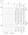
도 1은 몇몇 실시예에 따른 비휘발성 메모리 장치를 설명하기 위한 레이아웃도이다.
도 2는 도 1의 A-A를 따라 절단한 단면도이다.
도 3은 도 2의 R1 영역을 확대한 확대도이다.
도 4a 내지 도 4e는 도 2의 R2 영역을 확대한 다양한 확대도들이다.
도 5는 도 1의 B-B를 따라 절단한 단면도이다.
도 6은 도 1의 C-C를 따라 절단한 단면도이다.
도 7은 몇몇 실시예에 따른 비휘발성 메모리 장치를 설명하기 위한 레이아웃도이다.
도 8은 몇몇 실시예에 따른 비휘발성 메모리 장치를 설명하기 위한 레이아웃도이다.
도 9는 몇몇 실시예에 따른 비휘발성 메모리 장치를 설명하기 위한 레이아웃도이다.
도 10은 몇몇 실시예에 따른 비휘발성 메모리 장치를 설명하기 위한 레이아웃도이다.
도 11 내지 도 16은 몇몇 실시예에 따른 비휘발성 메모리 장치의 예시적인 제조 방법을 설명하기 위한 중간 단계 도면들이다.1 is a layout diagram for explaining a non-volatile memory device according to some embodiments.
Figure 2 is a cross-sectional view taken along AA of Figure 1.
Figure 3 is an enlarged view of the R1 region of Figure 2.
FIGS. 4A to 4E are various enlarged views of area R2 of FIG. 2.
Figure 5 is a cross-sectional view taken along BB of Figure 1.
Figure 6 is a cross-sectional view taken along CC of Figure 1.
Figure 7 is a layout diagram for explaining a non-volatile memory device according to some embodiments.
Figure 8 is a layout diagram for explaining a non-volatile memory device according to some embodiments.
9 is a layout diagram for explaining a non-volatile memory device according to some embodiments.
Figure 10 is a layout diagram for explaining a non-volatile memory device according to some embodiments.
11 to 16 are intermediate diagrams for explaining an exemplary manufacturing method of a non-volatile memory device according to some embodiments.
이하에서, 도 1 내지 도 10을 참조하여, 몇몇 실시예에 따른 비휘발성 메모리 장치를 설명한다.Hereinafter, a non-volatile memory device according to some embodiments will be described with reference to FIGS. 1 to 10 .
도 1은 몇몇 실시예에 따른 비휘발성 메모리 장치를 설명하기 위한 레이아웃도이다. 도 2는 도 1의 A-A를 따라 절단한 단면도이다. 도 3은 도 2의 R1 영역을 확대한 확대도이다. 도 4a 내지 도 4e는 도 2의 R2 영역을 확대한 다양한 확대도들이다. 도 5는 도 1의 B-B를 따라 절단한 단면도이다. 도 6은 도 1의 C-C를 따라 절단한 단면도이다.1 is a layout diagram for explaining a non-volatile memory device according to some embodiments. Figure 2 is a cross-sectional view taken along line A-A of Figure 1. Figure 3 is an enlarged view of the R1 region of Figure 2. FIGS. 4A to 4E are various enlarged views of area R2 of FIG. 2. Figure 5 is a cross-sectional view taken along line B-B of Figure 1. Figure 6 is a cross-sectional view taken along line C-C of Figure 1.
도 1 내지 도 6을 참조하면, 몇몇 실시예에 따른 비휘발성 메모리 장치는 기판(10), 주변 회로 구조체(PS), 몰드 구조체(MS), 복수의 채널 구조체(CS)들, 복수의 비트 라인(BL)들 및 소오스 구조체(200)를 포함한다.1 to 6, a non-volatile memory device according to some embodiments includes a
기판(10)은 예를 들어, 실리콘 기판, 게르마늄 기판 혹은 실리콘-게르마늄 기판 등과 같은 반도체 기판을 포함할 수 있다. 또는, 기판(10)은 실리콘-온-인슐레이터(SOI; Silicon-On-Insulator) 기판 혹은 게르마늄-온-인슐레이터(GOI; Germanium-On-Insulator) 기판 등을 포함할 수도 있다. 기판(10)은 예를 들어, p형 반도체 기판일 수 있으나, 이에 제한되는 것은 아니다.The
기판(10)은 셀 어레이 영역(CAR) 및 콘택 영역(CTR)을 포함할 수 있다.The
셀 어레이 영역(CAR)에는 복수의 메모리 셀들을 포함하는 메모리 셀 어레이가 형성될 수 있다. 메모리 셀 어레이는 복수의 메모리 셀들 및 각각의 상기 메모리 셀과 전기적으로 연결되는 복수의 워드 라인들 및 비트 라인들을 포함할 수 있다. 예를 들어, 셀 어레이 영역(CAR)에는 후술되는 비트 라인(BL), 몰드 구조체(MS), 채널 구조체(CS) 및 소오스 구조체(200)가 형성될 수 있다.A memory cell array including a plurality of memory cells may be formed in the cell array area CAR. A memory cell array may include a plurality of memory cells and a plurality of word lines and bit lines electrically connected to each memory cell. For example, a bit line (BL), a mold structure (MS), a channel structure (CS), and a
콘택 영역(CTR)은 셀 어레이 영역(CAR)의 주변에 배치될 수 있다. 콘택 영역(CTR)에는 예를 들어, 메모리 셀 콘택(310)들 및 관통 비아(THV)가 형성될 수 있다.The contact region (CTR) may be arranged around the cell array region (CAR). For example,
주변 회로 구조체(PS)는 기판(10) 상에 형성될 수 있다. 주변 회로 구조체(PS)는 각각의 메모리 셀의 동작을 제어하는 주변 회로를 구성할 수 있다. 예를 들어, 주변 회로 구조체(PS)는 로우 디코더(row decoder), 칼럼 디코더(column decoder), 페이지 버퍼(page buffer) 및 제어 회로 등을 포함할 수 있다. 예를 들어, 도 5에 도시된 것처럼, 주변 회로 구조체(PS)는 주변 회로 소자(PT) 및 배선 구조체(PW)를 포함할 수 있다.The peripheral circuit structure PS may be formed on the
몇몇 실시예에서, 주변 회로 소자(PT)는 트랜지스터(transistor)를 포함할 수 있다. 예를 들어, 주변 회로 소자(PT)는 주변 회로 게이트 전극(12), 주변 회로 게이트 절연막(14), 소오스/드레인 영역(16) 및 게이트 스페이서(18)를 포함할 수 있다.In some embodiments, the peripheral circuit element PT may include a transistor. For example, the peripheral circuit element PT may include a peripheral
주변 회로 게이트 전극(12)은 기판(10) 상에 형성될 수 있다. 주변 회로 게이트 전극(12)은 예를 들어, 실리콘(예를 들어, 폴리 실리콘), 금속 실리사이드(예를 들어, 텅스텐 실리사이드(WSi), 니켈 실리사이드(NiSi), 코발트 실리사이드(CoSi), 또는 티타늄 실리사이드(TiSi), 탄탈럼 실리사이드(TaSi)), 또는 금속(예를 들어, 텅스텐(W) 또는 알루미늄(Al)) 중 적어도 하나를 포함할 수 있으나, 이에 제한되는 것은 아니다. 몇몇 실시예에서, 주변 회로 게이트 전극(12)은 복수의 도전막으로 형성될 수도 있다.A peripheral
주변 회로 게이트 절연막(14)은 기판(10)과 주변 회로 게이트 전극(12) 사이에 개재될 수 있다. 예를 들어, 주변 회로 게이트 절연막(14)은 기판(10)의 상면을 따라 연장될 수 있다. 주변 회로 게이트 절연막(14)은 예를 들어, 실리콘 산화물, 실리콘 질화물, 실리콘 산질화물 및 실리콘 산화물보다 유전율이 큰 고유전율 물질 중 적어도 하나를 포함할 수 있으나, 이에 제한되는 것은 아니다.The peripheral circuit
소오스/드레인 영역(16)은 주변 회로 게이트 전극(12)의 양 측의 기판(10) 내에 형성될 수 있다. 소오스/드레인 영역(16)에는 불순물이 도핑될 수 있다. 예를 들어, 주변 회로 소자(PT)가 n형(또는 p형) 트랜지스터인 경우에, 소오스/드레인 영역(16)은 n형(또는 p형) 불순물로 도핑될 수 있다.Source/
게이트 스페이서(18)는 주변 회로 게이트 전극(12)의 양 측면 상에 형성될 수 있다. 예를 들어, 주변 회로 게이트 전극(12) 및 주변 회로 게이트 절연막(14)은, 기판(10)의 상면과 게이트 스페이서(18)의 내측면이 형성하는 트렌치를 채우도록 형성될 수 있다.
몇몇 실시예에서, 주변 회로 소자(PT)는 고전압 트랜지스터일 수 있다. 주변 회로 소자(PT)는 트랜지스터인 것만을 설명하였으나, 이는 예시적인 것일 뿐이고 본 발명의 기술적 사상이 이에 제한되는 것은 아니다. 예를 들어, 주변 회로 소자(PT)는 트랜지스터 등의 다양한 능동 소자(active element)뿐만 아니라, 커패시터(capacitor), 레지스터(resistor), 인덕터(inductor) 등의 다양한 수동 소자(passive element)를 포함할 수도 있다.In some embodiments, the peripheral circuit element PT may be a high voltage transistor. Although it has been explained that the peripheral circuit element (PT) is only a transistor, this is only an example and the technical idea of the present invention is not limited thereto. For example, peripheral circuit elements (PT) may include various active elements such as transistors, as well as various passive elements such as capacitors, resistors, and inductors. It may be possible.
몇몇 실시예에서, 주변 회로 소자(PT)는 웰 바이어스 구동 회로(driver)를 포함할 수 있다. 웰 바이어스 구동 회로는 각각의 메모리 셀의 소거 동작에 필요한 소거 전압을 채널 구조체(CS)에 제공할 수 있다.In some embodiments, the peripheral circuit element PT may include a well bias driving circuit (driver). The well bias driving circuit may provide the channel structure CS with an erase voltage required for an erase operation of each memory cell.
몇몇 실시예에서, 기판(10) 상에 제1 층간 절연막(20)이 형성될 수 있다. 제1 층간 절연막(20)은 기판(10) 상의 주변 회로 소자(PT)를 덮도록 형성될 수 있다. 제1 층간 절연막(20)은 단일막인 것으로 도시되었으나, 이는 설명의 편의를 위한 것일 뿐이고, 제1 층간 절연막(20)은 복수의 절연막이 적층된 다중막일 수도 있음은 물론이다. 제1 층간 절연막(20)은 예를 들어, 실리콘 산화물을 포함할 수 있으나, 이에 제한되는 것은 아니다.In some embodiments, a first
배선 구조체(PW)는 주변 회로 배선(22)들 및 주변 회로 콘택(24)들을 포함할 수 있다. 주변 회로 배선(22)들 및 주변 회로 콘택(24)들은 예를 들어, 제1 층간 절연막(20) 내에 형성될 수 있다. 주변 회로 배선(22)들은 주변 회로 콘택(24)들을 통해 주변 회로 소자(PT)와 연결될 수 있다.The interconnection structure PW may include
주변 회로 배선(22)들은 예를 들어, 금속(예를 들어, 구리(Cu) 또는 알루미늄(Al))을 포함할 수 있으나, 이에 제한되는 것은 아니다. 주변 회로 콘택(24)들은 예를 들어, 실리콘(예를 들어, 폴리 실리콘) 또는 금속(예를 들어, 텅스텐(W) 또는 구리(Cu))을 포함할 수 있으나, 이에 제한되는 것은 아니다.The
몰드 구조체(MS)는 주변 회로 구조체(PS) 상에 형성될 수 있다. 예를 들어, 몰드 구조체(MS)는 제1 층간 절연막(20) 상에 형성될 수 있다. 즉, 주변 회로 구조체(PS)는 기판(10)과 몰드 구조체(MS) 사이에 개재될 수 있다. 몰드 구조체(MS)는 주변 회로 구조체(PS) 상에 적층되는 복수의 게이트 전극(SSL, DM1, WL1~WLn, DM2, GSL)들 및 복수의 절연 패턴(110)들을 포함할 수 있다. 각각의 게이트 전극(SSL, DM1, WL1~WLn, DM2, GSL) 및 각각의 절연 패턴(110)은 제1 방향(X) 및 제1 방향(X)과 교차하는 제2 방향(Y)으로 연장되는 층상 구조일 수 있다.The mold structure MS may be formed on the peripheral circuit structure PS. For example, the mold structure MS may be formed on the first
각각의 게이트 전극(SSL, DM1, WL1~WLn, DM2, GSL)은 각각의 절연 패턴(110)과 교대로 적층될 수 있다. 예를 들어, 게이트 전극(SSL, DM1, WL1~WLn, DM2, GSL)들은 기판(10)의 상면과 교차하는 제3 방향(Z)을 따라 서로 이격되며 순차적으로 적층될 수 있다. 이 때, 절연 패턴(110)들은 게이트 전극(SSL, DM1, WL1~WLn, DM2, GSL)들 사이에 개재될 수 있다. 즉, 게이트 전극(SSL, DM1, WL1~WLn, DM2, GSL)들은 절연 패턴(110)에 의해 전기적으로 서로 이격될 수 있다.Each gate electrode (SSL, DM1, WL1 to WLn, DM2, GSL) may be alternately stacked with each insulating
도 2, 도 5 및 도 6에서, 게이트 전극(SSL, DM1, WL1~WLn, DM2, GSL)들은 서로 동일한 두께를 갖는 것으로 도시되었으나, 이는 예시적인 것일 뿐이다. 예를 들어, 게이트 전극(SSL, DM1, WL1~WLn, DM2, GSL)들은 서로 다른 두께를 가질 수도 있다.In FIGS. 2, 5, and 6, the gate electrodes (SSL, DM1, WL1 to WLn, DM2, and GSL) are shown to have the same thickness, but this is only an example. For example, the gate electrodes (SSL, DM1, WL1 to WLn, DM2, GSL) may have different thicknesses.
몇몇 실시예에서, 게이트 전극(SSL, DM1, WL1~WLn, DM2, GSL)들은 스트링 선택 라인(SSL), 복수의 워드 라인(WL1~WLn)들 및 그라운드 선택 라인(GSL)을 포함할 수 있다. 스트링 선택 라인(SSL), 복수의 워드 라인(WL1~WLn)들 및 그라운드 선택 라인(GSL)은 기판(10) 상에 순차적으로 적층될 수 있다.In some embodiments, the gate electrodes (SSL, DM1, WL1 to WLn, DM2, GSL) may include a string select line (SSL), a plurality of word lines (WL1 to WLn), and a ground select line (GSL). . A string select line (SSL), a plurality of word lines (WL1 to WLn), and a ground select line (GSL) may be sequentially stacked on the
스트링 선택 라인(SSL)은, 비트 라인(BL)과 각각의 채널 구조체(CS) 사이의 전기적 연결을 제어하는 스트링 선택 트랜지스터의 게이트 전극으로 기능할 수 있다. 복수의 워드 라인(WL1~WLn)들은, 각각의 메모리 셀을 제어하는 메모리 셀 트랜지스터의 게이트 전극으로 기능할 수 있다. 즉, 복수의 워드 라인(WL1~WLn)들은, 채널 구조체(CS)와 함께 복수의 메모리 셀들을 구성할 수 있다. 그라운드 선택 라인(GSL)은, 소오스 구조체(200)와 각각의 채널 구조체(CS) 사이의 전기적 연결을 제어하는 그라운드 선택 트랜지스터의 게이트 전극으로 기능할 수 있다.The string select line (SSL) may function as a gate electrode of a string select transistor that controls the electrical connection between the bit line (BL) and each channel structure (CS). A plurality of word lines (WL1 to WLn) may function as a gate electrode of a memory cell transistor that controls each memory cell. That is, the plurality of word lines (WL1 to WLn) together with the channel structure (CS) may form a plurality of memory cells. The ground select line (GSL) may function as a gate electrode of a ground select transistor that controls the electrical connection between the
스트링 선택 라인(SSL)과 그라운드 선택 라인(GSL) 사이에 3개의 워드 라인만을 간략하게 도시하였으나, 이는 설명의 편의를 위한 것일 뿐이다. 예를 들어, 스트링 선택 라인(SSL)과 그라운드 선택 라인(GSL) 사이에 8개, 16개, 32개, 64개 또는 그 이상의 워드 라인들이 적층될 수 있음은 물론이다.Only three word lines are briefly shown between the string select line (SSL) and the ground select line (GSL), but this is only for convenience of explanation. For example, of course, 8, 16, 32, 64 or more word lines can be stacked between the string select line (SSL) and the ground select line (GSL).
또한, 몰드 구조체(MS)는 1개의 스트링 선택 라인(SSL) 및 1개의 그라운드 선택 라인(GSL)만을 갖는 것으로 간략하게 도시하였으나, 이는 설명의 편의를 위한 것일 뿐이다. 예를 들어, 몰드 구조체(MS)는 2개 이상의 스트링 선택 라인(SSL) 또는 2개 이상의 그라운드 선택 라인(GSL)을 가질 수 있음은 물론이다.In addition, the mold structure MS is briefly shown as having only one string selection line (SSL) and one ground selection line (GSL), but this is only for convenience of explanation. For example, the mold structure MS may have two or more string selection lines (SSL) or two or more ground selection lines (GSL).
몇몇 실시예에서, 몰드 구조체(MS)는 제1 더미 라인(DM1) 및/또는 제2 더미 라인(DM2)을 더 포함할 수 있다. 제1 더미 라인(DM1)은 예를 들어, 스트링 선택 라인(SSL)과 복수의 워드 라인(WL1~WLn)들 사이에 개재될 수 있다. 제2 더미 라인(DM2)은 예를 들어, 그라운드 선택 라인(GSL)과 복수의 워드 라인(WL1~WLn)들 사이에 개재될 수 있다. 몇몇 실시예에 따른 비휘발성 메모리 장치에서, 제1 더미 라인(DM1) 및 제2 더미 라인(DM2)은 스트링 선택 라인, 워드 라인 또는 그라운드 선택 라인으로 기능하지 않을 수 있다.In some embodiments, the mold structure MS may further include a first dummy line DM1 and/or a second dummy line DM2. For example, the first dummy line DM1 may be interposed between the string selection line SSL and the plurality of word lines WL1 to WLn. For example, the second dummy line DM2 may be interposed between the ground select line GSL and the plurality of word lines WL1 to WLn. In the non-volatile memory device according to some embodiments, the first dummy line DM1 and the second dummy line DM2 may not function as a string select line, word line, or ground select line.
각각의 게이트 전극(SSL, DM1, WL1~WLn, DM2, GSL)은 도전성 물질을 포함할 수 있다. 예를 들어, 각각의 게이트 전극(SSL, DM1, WL1~WLn, DM2, GSL)은 텅스텐(W), 코발트(Co), 니켈(Ni) 등의 금속이나 실리콘과 같은 반도체 물질을 포함할 수 있으나, 이에 제한되는 것은 아니다.Each gate electrode (SSL, DM1, WL1 to WLn, DM2, GSL) may include a conductive material. For example, each gate electrode (SSL, DM1, WL1~WLn, DM2, GSL) may contain a metal such as tungsten (W), cobalt (Co), or nickel (Ni) or a semiconductor material such as silicon. , but is not limited to this.
각각의 절연 패턴(110)은 절연성 물질을 포함할 수 있다. 예를 들어, 각각의 절연 패턴(110)은 실리콘 산화물을 포함할 수 있으나, 이에 제한되는 것은 아니다.Each insulating
몇몇 실시예에서, 제1 층간 절연막(20) 상에 제2 층간 절연막(30)이 형성될 수 있다. 제2 층간 절연막(30)은 몰드 구조체(MS)의 적어도 일부를 덮도록 형성될 수 있다. 제2 층간 절연막(30)은 단일막인 것으로 도시되었으나, 이는 설명의 편의를 위한 것일 뿐이고, 제2 층간 절연막(30)은 복수의 절연막이 적층된 다중막일 수도 있음은 물론이다. 제2 층간 절연막(30)은 예를 들어, 실리콘 산화물을 포함할 수 있으나, 이에 제한되는 것은 아니다.In some embodiments, a second
몇몇 실시예에서, 도 2에 도시된 것처럼, 각각의 게이트 전극(SSL, DM1, WL1~WLn, DM2, GSL)과 접속되는 메모리 셀 콘택(310)들 및 제1 상부 배선(315)들이 형성될 수 있다. 메모리 셀 콘택(310)들은 각각의 게이트 전극(SSL, DM1, WL1~WLn, DM2, GSL)의 단부 상에 형성될 수 있다. 예를 들어, 메모리 셀 콘택(310)들은 콘택 영역(CTR) 상에 형성될 수 있다.In some embodiments, as shown in FIG. 2,
메모리 셀 콘택(310)은 각각의 게이트 전극(SSL, DM1, WL1~WLn, DM2, GSL)과 접속되도록 형성될 수 있다. 예를 들어, 메모리 셀 콘택(310)은 제2 층간 절연막(30)을 관통하여 각각의 게이트 전극(SSL, DM1, WL1~WLn, DM2, GSL)과 접속될 수 있다.The
제1 상부 배선(315)은 메모리 셀 콘택(310) 상에 형성될 수 있다. 예를 들어, 제1 상부 배선(315)은 제2 층간 절연막(30) 상의 제3 층간 절연막(40) 내에 형성될 수 있다. 이에 따라, 제1 상부 배선(315)은 각각의 게이트 전극(SSL, DM1, WL1~WLn, DM2, GSL)과 전기적으로 접속되어, 각각의 게이트 전극(SSL, DM1, WL1~WLn, DM2, GSL)에 게이트 전압을 인가할 수 있다.The first
몇몇 실시예에서, 주변 회로 구조체(PS)와 접속되는 관통 비아(THV) 및 제2 상부 배선(325)이 형성될 수 있다. 예를 들어, 관통 비아(THV)는 제2 층간 절연막(30)을 관통하여 배선 구조체(PW)와 접속될 수 있다. 제2 상부 배선(325)은 관통 비아(THV) 상에 형성될 수 있다. 예를 들어, 제2 상부 배선(325)은 제3 층간 절연막(40) 내에 형성될 수 있다.In some embodiments, a through via (THV) and a second
제1 상부 배선(315) 및 제2 상부 배선(325)은 예를 들어, 금속(예를 들어, 구리(Cu) 또는 알루미늄(Al))을 포함할 수 있으나, 이에 제한되는 것은 아니다. 메모리 셀 콘택(310) 및 관통 비아(THV)는 예를 들어, 실리콘(예를 들어, 폴리 실리콘) 또는 금속(예를 들어, 텅스텐(W) 또는 구리(Cu))을 포함할 수 있으나, 이에 제한되는 것은 아니다.The first
몇몇 실시예에서, 몰드 구조체(MS)는 워드 라인 절단 영역(WLc)에 의해 절단될 수 있다. 예를 들어, 도 1, 도 5 및 도 6에 도시된 것처럼, 워드 라인 절단 영역(WLc)은 제2 방향(Y)으로 연장되어 몰드 구조체(MS)를 절단할 수 있다.In some embodiments, the mold structure MS may be cut by the word line cutting area WLc. For example, as shown in FIGS. 1, 5, and 6, the word line cutting area WLc may extend in the second direction Y to cut the mold structure MS.
몇몇 실시예에서, 워드 라인 절단 영역(WLc) 내에 절연 구조체(150)가 형성될 수 있다. 절연 구조체(150)는 워드 라인 절단 영역(WLc)을 채우도록 형성될 수 있다. 도 5 및 도 6에 도시된 것처럼, 절연 구조체(150)는 몰드 구조체(MS)를 관통하여 제1 층간 절연막(20)까지 연장될 수 있다. 이에 따라, 절연 구조체(150)는 제2 방향(Y)으로 연장되며 몰드 구조체(MS)를 절단할 수 있다.In some embodiments, an insulating
절연 구조체(150)는 예를 들어, 실리콘 산화물, 실리콘 질화물, 실리콘 산질화물 및 실리콘 산화물보다 유전율이 큰 고유전율 물질 중 적어도 하나를 포함할 수 있으나, 이에 제한되는 것은 아니다.The insulating
복수의 채널 구조체(CS)들은 몰드 구조체(MS)를 관통할 수 있다. 또한, 복수의 채널 구조체(CS)들은 복수의 게이트 전극(SSL, DM1, WL1~WLn, DM2, GSL)들과 교차하는 방향으로 연장될 수 있다. 예를 들어, 각각의 채널 구조체(CS)는 제3 방향(Z)으로 연장되는 필러(pillar) 모양(예를 들어, 원기둥 모양)일 수 있다. 각각의 채널 구조체(CS)는 반도체 패턴(120) 및 정보 저장막(130)을 포함할 수 있다.A plurality of channel structures (CS) may penetrate the mold structure (MS). Additionally, the plurality of channel structures CS may extend in a direction intersecting the plurality of gate electrodes SSL, DM1, WL1 to WLn, DM2, and GSL. For example, each channel structure CS may have a pillar shape (eg, a cylinder shape) extending in the third direction (Z). Each channel structure CS may include a
반도체 패턴(120)은 몰드 구조체(MS)를 관통할 수 있다. 예를 들어, 반도체 패턴(120)은 제3 방향(Z)으로 연장될 수 있다. 반도체 패턴(120)은 컵(cup) 형상인 것으로 도시되었으나, 이는 예시적인 것일 뿐이다. 예를 들어, 반도체 패턴(120)은 원통 형상, 사각통 형상, 속이 찬 필러 형상 등 다양한 형상을 가질 수도 있다.The
반도체 패턴(120)은 예를 들어, 단결정 실리콘, 다결정 실리콘, 유기 반도체물 및 탄소 나노 구조체 등의 반도체 물질을 포함할 수 있으나, 이에 제한되는 것은 아니다.The
정보 저장막(130)은 반도체 패턴(120)과 각각의 게이트 전극(SSL, DM1, WL1~WLn, DM2, GSL) 사이에 개재될 수 있다. 예를 들어, 정보 저장막(130)은 반도체 패턴(120)의 측면을 따라 연장될 수 있다.The
정보 저장막(130)은 예를 들어, 실리콘 산화물, 실리콘 질화물, 실리콘 산질화물 및 실리콘 산화물보다 유전율이 큰 고유전율 물질 중 적어도 하나를 포함할 수 있다. 상기 고유전율 물질은 예를 들어, 알루미늄 산화물(aluminum oxide), 하프늄 산화물(hafnium oxide), 란타늄 산화물(lanthanum oxide), 탄탈륨 산화물(tantalum oxide), 티타늄 산화물(titanium oxide), 란타늄 하프늄 산화물(lanthanum hafnium oxide), 란타늄 알루미늄 산화물(lanthanum aluminum oxide), 디스프로슘 스칸듐 산화물(dysprosium scandium oxide) 및 이들의 조합 중 적어도 하나를 포함할 수 있다.The
몇몇 실시예에서, 정보 저장막(130)은 복수의 막을 포함할 수 있다. 예를 들어, 도 3에 도시된 것처럼, 정보 저장막(130)은 반도체 패턴(120) 상에 차례로 적층되는 터널 절연막(132), 전하 저장막(134) 및 제1 블로킹 절연막(136)을 포함할 수 있다.In some embodiments, the
터널 절연막(132)은 예를 들어, 실리콘 산화물 또는 실리콘 산화물보다 높은 유전율을 갖는 고유전율 물질(예를 들어, 알루미늄 산화물(Al2O3), 하프늄 산화물(HfO2))을 포함할 수 있다. 전하 저장막(134)은 예를 들어, 실리콘 질화물을 포함할 수 있다. 제1 블로킹 절연막(136)은 예를 들어, 실리콘 산화물 또는 실리콘 산화물보다 높은 유전율을 갖는 고유전율 물질(예를 들어, 알루미늄 산화물(Al2O3), 하프늄 산화물(HfO2))을 포함할 수 있다.The
몇몇 실시예에서, 각각의 채널 구조체(CS)는 제2 블로킹 절연막(138)을 더 포함할 수 있다. 제2 블로킹 절연막(138)은 정보 저장막(130)과 각각의 게이트 전극(SSL, DM1, WL1~WLn, DM2, GSL) 사이에 개재될 수 있다. 예를 들어, 제2 블로킹 절연막(138)은 각각의 게이트 전극(SSL, DM1, WL1~WLn, DM2, GSL)의 측면을 따라 연장될 수 있다.In some embodiments, each channel structure CS may further include a second blocking insulating
몇몇 실시예에서, 제2 블로킹 절연막(138)은 각각의 게이트 전극(SSL, DM1, WL1~WLn, DM2, GSL)의 상면 및 하면을 따라 더 연장될 수 있다. 이에 따라, 제2 블로킹 절연막(138)은 각각의 게이트 전극(SSL, DM1, WL1~WLn, DM2, GSL)과 각각의 절연 패턴(110) 사이에도 개재될 수 있다.In some embodiments, the second blocking insulating
몇몇 실시예에서, 각각의 채널 구조체(CS)는 충진 절연 패턴(140)을 더 포함할 수 있다. 충진 절연 패턴(140)은 컵 형상인 반도체 패턴(120)의 내부를 채우도록 형성될 수 있다. 예를 들어, 반도체 패턴(120)은 충진 절연 패턴(140)의 측면 및 바닥면을 따라 연장될 수 있다. 충진 절연 패턴(140)은 예를 들어, 실리콘 산화물을 포함할 수 있으나, 이에 제한되는 것은 아니다.In some embodiments, each channel structure CS may further include a filling insulating
몇몇 실시예에서, 복수의 채널 구조체(CS)들은 제1 방향(X) 및 제2 방향(Y)을 따라 반복적으로 배열될 수 있다. 예를 들어, 도 1에 도시된 것처럼, 복수의 채널 구조체(CS)들 중 일부는, 제1 방향(X)을 따라 배열되어 제1 채널 그룹(CG1)을 형성할 수 있다. 또한, 복수의 채널 구조체(CS)들 중 다른 일부는, 제1 방향(X)을 따라 배열되어 제2 채널 그룹(CG2)을 형성할 수 있다. 제1 채널 그룹(CG1) 및 제2 채널 그룹(CG2)은 서로 인접하며 나란히 배열될 수 있다. 예를 들어, 제2 채널 그룹(CG2)은 제2 방향(Y)에서 제1 채널 그룹(CG1)과 인접할 수 있다.In some embodiments, the plurality of channel structures CS may be repeatedly arranged along the first direction (X) and the second direction (Y). For example, as shown in FIG. 1, some of the plurality of channel structures CS may be arranged along the first direction X to form the first channel group CG1. Additionally, other portions of the plurality of channel structures CS may be arranged along the first direction X to form the second channel group CG2. The first channel group CG1 and the second channel group CG2 are adjacent to each other and may be arranged side by side. For example, the second channel group CG2 may be adjacent to the first channel group CG1 in the second direction (Y).
몇몇 실시예에서, 복수의 채널 구조체(CS)들은 지그재그(zigzag) 형태로 배열될 수 있다. 예를 들어, 도 1에 도시된 것처럼, 제1 채널 그룹(CG1)을 구성하는 채널 구조체(CS)들 및 제2 채널 그룹(CG2)을 구성하는 채널 구조체(CS)들은, 제2 방향(Y)에서 서로 엇갈리게 배열될 수 있다. 지그재그 형태로 배열된 복수의 채널 구조체(CS)들은 몇몇 실시예에 따른 비휘발성 메모리 장치의 집적도를 보다 향상시킬 수 있다.In some embodiments, the plurality of channel structures CS may be arranged in a zigzag shape. For example, as shown in FIG. 1, the channel structures (CS) constituting the first channel group (CG1) and the channel structures (CS) constituting the second channel group (CG2) are aligned in the second direction (Y). ) can be arranged in a staggered manner. A plurality of channel structures (CS) arranged in a zigzag shape can further improve the integration of a non-volatile memory device according to some embodiments.
도 1에서, 제1 채널 그룹(CG1)을 구성하는 채널 구조체(CS)들의 개수(예를 들어, 4개)는, 제2 채널 그룹(CG2)을 구성하는 채널 구조체(CS)들의 개수(예를 들어, 5개)보다 적은 것으로 도시되었으나, 이는 예시적인 것일 뿐이다. 예를 들어, 복수의 채널 구조체(CS)들이 지그재그(zigzag) 형태로 배열되더라도, 제1 채널 그룹(CG1)을 구성하는 채널 구조체(CS)들의 개수는 제2 채널 그룹(CG2)을 구성하는 채널 구조체(CS)들의 개수와 동일할 수도 있다.In FIG. 1, the number (e.g., 4) of channel structures (CS) constituting the first channel group (CG1) is the number (e.g., 4) of channel structures (CS) constituting the second channel group (CG2). For example, it is shown as less than 5), but this is only illustrative. For example, even if a plurality of channel structures (CS) are arranged in a zigzag shape, the number of channel structures (CS) constituting the first channel group (CG1) is less than the number of channel structures (CS) constituting the second channel group (CG2). It may be equal to the number of structures (CS).
복수의 비트 라인(BL)들은 2차원적으로 배열될 수 있다. 예를 들어, 각각의 비트 라인(BL)은 서로 이격되어 제1 방향(X)으로 나란히 연장될 수 있다. 워드 라인 절단 영역(WLc)은 제2 방향(Y)으로 연장될 수 있으므로, 각각의 비트 라인(BL)은 워드 라인 절단 영역(WLc)과 교차할 수 있다.A plurality of bit lines BL may be arranged two-dimensionally. For example, each bit line BL may be spaced apart from each other and extend parallel to each other in the first direction (X). Since the word line cut area (WLc) may extend in the second direction (Y), each bit line (BL) may intersect the word line cut area (WLc).
각각의 비트 라인(BL)에는 채널 구조체(CS)가 연결될 수 있다. 예를 들어, 각각의 비트 라인(BL)은 비트 라인 콘택(BLc)을 통해 각각의 채널 구조체(CS)와 접속될 수 있다.A channel structure (CS) may be connected to each bit line (BL). For example, each bit line BL may be connected to each channel structure CS through a bit line contact BLc.
몇몇 실시예에서, 비트 라인(BL)은 몰드 구조체(MS) 아래에 형성될 수 있다. 즉, 비트 라인(BL)은 기판(10)과 몰드 구조체(MS) 사이에 개재될 수 있다. 예를 들어, 비트 라인(BL) 및 비트 라인 콘택(BLc)은 제1 층간 절연막(20) 내에 형성될 수 있다. 비트 라인 콘택(BLc)은 채널 구조체(CS)와 비트 라인(BL) 사이에 개재되어, 반도체 패턴(120)과 비트 라인(BL)을 연결할 수 있다. 이에 따라, 각각의 비트 라인(BL)은 반도체 패턴(120)의 하부와 접속될 수 있다.In some embodiments, the bit line BL may be formed below the mold structure MS. That is, the bit line BL may be interposed between the
몇몇 실시예에서, 채널 구조체(CS)와 비트 라인(BL) 사이에 스터드(105)가 형성될 수 있다. 예를 들어, 스터드(105)는 제1 층간 절연막(20) 내에 형성될 수 있다. 스터드(105)는 채널 구조체(CS)와 비트 라인(BL)을 연결할 수 있다. 예를 들어, 스터드(105)의 상면은 반도체 패턴(120)의 하면과 접촉할 수 있고, 스터드(105)의 하면은 비트 라인 콘택(BLc)의 상면과 접촉할 수 있다. 스터드(105)는 예를 들어, 폴리 실리콘을 포함할 수 있으나, 이에 제한되는 것은 아니다.In some embodiments,
몇몇 실시예에서, 스터드(105)의 폭은 채널 구조체(CS)의 폭 및 비트 라인 콘택(BLc)의 폭보다 클 수 있다. 이에 따라, 스터드(105)는 반도체 패턴(120)과 비트 라인 콘택(BLc)을 안정적으로 연결할 수 있다.In some embodiments, the width of the
소오스 구조체(200)는 몰드 구조체(MS) 상에 형성될 수 있다. 또한, 소오스 구조체(200)는 셀 어레이 영역(CAR) 상에 형성되어, 각각의 채널 구조체(CS)의 상부와 접속될 수 있다.The
소오스 구조체(200)는 제1 불순물 패턴(210) 및 제2 불순물 패턴(220)을 포함할 수 있다. 제1 불순물 패턴(210)은 각각의 채널 구조체(CS)의 일부와 접속될 수 있고, 제2 불순물 패턴(220)은 각각의 채널 구조체(CS)의 다른 일부와 접속될 수 있다. 몇몇 실시예에서, 제1 불순물 패턴(210) 및 제2 불순물 패턴(220)은 반도체 패턴(120)의 상면과 접촉할 수 있다.The
몇몇 실시예에서, 제1 불순물 패턴(210)은 제1 도전형을 가질 수 있고, 제2 불순물 패턴(220)은 상기 제1 도전형과 다른 제2 도전형을 가질 수 있다. 이하에서, 설명의 편의를 위해, 제1 불순물 패턴(210)은 n형 불순물을 포함하고, 제2 불순물 패턴(220)은 p형 불순물을 포함하는 것으로 설명한다. 그러나, 이는 예시적인 것일 뿐이고, 본 발명의 기술적 사상이 이에 제한되는 것은 아니다. 예를 들어, 제1 불순물 패턴(210)은 p형 불순물을 포함하고, 제2 불순물 패턴(220)은 n형 불순물을 포함할 수도 있음은 물론이다.In some embodiments, the
몇몇 실시예에서, 제1 불순물 패턴(210)의 상면은 제2 불순물 패턴(220)의 상면과 동일 평면 상에 배치될 수 있다. 본 명세서에서, "동일"이란, 완전히 동일한 것뿐만 아니라 공정 상의 마진 등으로 인해 발생할 수 있는 미세한 차이를 포함하는 의미이다.In some embodiments, the top surface of the
몇몇 실시예에서, 소오스 구조체(200)는 분리 패턴(230)을 더 포함할 수 있다. 분리 패턴(230)은 제1 불순물 패턴(210)과 제2 불순물 패턴(220) 사이에 개재되어, 제1 불순물 패턴(210)과 제2 불순물 패턴(220)을 분리할 수 있다.In some embodiments, the
분리 패턴(230)은 절연 물질을 포함할 수 있다. 분리 패턴(230)은 예를 들어, 실리콘 산화물, 실리콘 질화물 및 실리콘 산질화물 중 적어도 하나를 포함할 수 있으나, 이에 제한되는 것은 아니다.The
몇몇 실시예에서, 제1 불순물 패턴(210)의 상면 및 제2 불순물 패턴(220)의 상면은 분리 패턴(230)의 상면과 동일 평면 상에 배치될 수 있다.In some embodiments, the top surface of the
몇몇 실시예에서, 제1 불순물 패턴(210)은 각각의 채널 구조체(CS)의 일부와 중첩될 수 있고, 제2 불순물 패턴(220)은 각각의 채널 구조체(CS)의 다른 일부와 중첩될 수 있다. 여기서, 중첩이란, 기판(10)의 상면과 교차하는 제3 방향(Z)에서 중첩됨을 의미한다.In some embodiments, the
예를 들어, 도 1 및 도 4a에 도시된 것처럼, 평면적 관점에서, 각각의 채널 구조체(CS)는 서로 구분되는 제1 영역(CSa), 제2 영역(CSb) 및 제3 영역(CSc)을 포함할 수 있다. 제3 영역(CSc)은 제1 영역(CSa)과 제2 영역(CSb) 사이에 개재될 수 있다. 이 때, 제1 불순물 패턴(210)은 각각의 채널 구조체(CS)의 제1 영역(CSa)과 중첩될 수 있고, 제2 불순물 패턴(220)은 각각의 채널 구조체(CS)의 제2 영역(CSb)과 중첩될 수 있다. 분리 패턴(230)은 각각의 채널 구조체(CS)의 제3 영역(CSc)과 중첩될 수 있다.For example, as shown in FIGS. 1 and 4A, from a plan view, each channel structure (CS) has a first region (CSa), a second region (CSb), and a third region (CSc) that are distinct from each other. It can be included. The third area CSc may be interposed between the first area CSa and the second area CSb. At this time, the
몇몇 실시예에서, 제1 도전형(예를 들어, n형)을 갖는 제1 불순물 패턴(210)은 공통 소오스 라인(CSL; common source line)으로 기능할 수 있다. 예를 들어, 몇몇 실시예에 따른 비휘발성 메모리 장치의 읽기(read) 동작 또는 쓰기(write) 동작 시에, 제1 불순물 패턴(210)에 접지 전압이 인가될 수 있다.In some embodiments, the
몇몇 실시예에서, 제2 도전형(예를 들어, p형)을 갖는 제2 불순물 패턴(220)은, 몇몇 실시예에 따른 비휘발성 메모리 장치의 소거(erase) 동작에 이용될 수 있다. 예를 들어, 몇몇 실시예에 따른 비휘발성 메모리 장치의 소거 동작 시에, 제2 불순물 패턴(220)에 소거 전압이 인가될 수 있다.In some embodiments, the
몇몇 실시예에 따른 비휘발성 메모리 장치에서, 제2 불순물 패턴(220)은 제1 불순물 패턴(210)의 제1 도전형(예를 들어, n형)과 다른 제2 도전형(예를 들어, p형)을 가지므로, 비휘발성 메모리 장치의 소거 동작의 소모 전력을 줄이고 소거 신뢰성을 향상시킬 수 있다. 예를 들어, 몇몇 실시예에 따른 비휘발성 메모리 장치의 소거 동작 시에, 정공(hole)들은 p형 불순물을 포함하는 제2 불순물 패턴(220)을 통해 각각의 채널 구조체(CS)에 원활히 공급될 수 있다. 이에 따라, 동작 성능 및 신뢰성이 향상된 비휘발성 메모리 장치가 제공될 수 있다.In a non-volatile memory device according to some embodiments, the
몇몇 실시예에 따른 비휘발성 메모리 장치에서, 분리 패턴(230)은 서로 다른 도전형을 갖는 제1 불순물 패턴(210) 및 제2 불순물 패턴(220)이 P-N 접합을 이루는 것을 방지할 수 있다. 즉, 분리 패턴(230)은 제1 불순물 패턴(210) 및 제2 불순물 패턴(220) 사이에서 발생되는 접합 누설 전류(junction leakage)를 방지함으로써, 제2 불순물 패턴(220)의 저항을 감소시킬 수 있다. 예를 들어, 몇몇 실시예에 따른 비휘발성 메모리 장치의 소거 동작 시에, 정공(hole)들은 p형 불순물을 포함하는 제2 불순물 패턴(220)을 통해 각각의 채널 구조체(CS)에 빠르게 공급될 수 있다. 이에 따라, 동작 성능 및 신뢰성이 더욱 향상된 비휘발성 메모리 장치가 제공될 수 있다.In a non-volatile memory device according to some embodiments, the
몇몇 실시예에서, 제1 불순물 패턴(210)의 측면은 곡면을 가질 수 있다. 예를 들어, 도 4b에 도시된 것처럼, 제1 불순물 패턴(210)은 곡면을 포함하는 제1 측면(210S)을 포함할 수 있다. 몇몇 실시예에서, 제1 측면(210S)은 오목할 수 있다.In some embodiments, a side surface of the
몇몇 실시예에서, 분리 패턴(230) 및 제2 불순물 패턴(220)은 제1 측면(210S)에 대응되는 모양을 가질 수 있다. 예를 들어, 분리 패턴(230)은 오목한 제1 측면(210S)의 프로파일을 따라 연장되어 휘어진 모양을 가질 수 있다. 또한, 예를 들어, 제2 불순물 패턴(220)은 제1 측면(210S)에 대향되는 제2 측면(220S)을 포함할 수 있다. 제2 측면(220S)은 오목한 제1 측면(210S)의 프로파일을 따라 연장되어 볼록할 수 있다.In some embodiments, the
몇몇 실시예에서, 제1 불순물 패턴(210)의 측면은 경사를 가질 수 있다. 예를 들어, 도 4c에 도시된 것처럼, 제1 불순물 패턴(210)의 제1 측면(210S)은 채널 구조체(CS)의 상면에 대하여 경사를 가질 수 있다. 몇몇 실시예에서, 제1 측면(210S)은 채널 구조체(CS)의 상면에 대하여 예각을 이룰 수 있다.In some embodiments, a side surface of the
몇몇 실시예에서, 분리 패턴(230) 및 제2 불순물 패턴(220)은 제1 측면(210S)에 대응되는 모양을 가질 수 있다. 예를 들어, 분리 패턴(230)은 경사를 갖는 제1 측면(210S)의 프로파일을 따라 연장되어 경사를 가질 수 있다. 또한, 예를 들어, 제2 측면(220S)은, 채널 구조체(CS)의 상면에 대하여 예각을 이루는 제1 측면(210S)의 프로파일을 따라 연장되어, 채널 구조체(CS)의 상면에 대하여 둔각을 이룰 수 있다.In some embodiments, the
몇몇 실시예에서, 제1 불순물 패턴(210)이 채널 구조체(CS)와 중첩되는 영역의 크기는, 제2 불순물 패턴(220)이 채널 구조체(CS)와 중첩되는 영역의 크기와 다를 수 있다. 예를 들어, 도 4d 및 도 4e에 도시된 것처럼, 제1 불순물 패턴(210)과 중첩되는 제1 영역(CSa)의 크기는 제2 불순물 패턴(220)과 중첩되는 제2 영역(CSb)의 크기와 다를 수 있다.In some embodiments, the size of the area where the
예를 들어, 도 4d에 도시된 것처럼, 제2 방향(Y)에서, 제1 불순물 패턴(210)과 채널 구조체(CS)가 중첩되는 제1 중첩 길이(OL1)는, 제2 불순물 패턴(220)과 채널 구조체(CS)가 중첩되는 제2 중첩 길이(OL2)보다 작을 수 있다.For example, as shown in FIG. 4D, in the second direction Y, the first overlap length OL1 where the
또는, 예를 들어, 도 4e에 도시된 것처럼, 제2 방향(Y)에서, 제1 불순물 패턴(210)과 채널 구조체(CS)가 중첩되는 제1 중첩 길이(OL1)는, 제2 불순물 패턴(220)과 채널 구조체(CS)가 중첩되는 제2 중첩 길이(OL2)보다 클 수도 있다.Or, for example, as shown in FIG. 4E, in the second direction Y, the first overlap length OL1 where the
몇몇 실시예에서, 도 5 및 도 6에 도시된 것처럼, 소오스 구조체(200)와 접속되는 제1 상부 콘택(48), 제3 상부 배선(46), 제2 상부 콘택(44) 및 제4 상부 배선(42)이 형성될 수 있다.In some embodiments, as shown in FIGS. 5 and 6, the first
제1 상부 콘택(48)은 제1 불순물 패턴(210)과 접속되도록 형성될 수 있다. 에를 들어, 제1 상부 콘택(48)은 제3 층간 절연막(40)을 관통하여 제1 불순물 패턴(210)과 접속될 수 있다. 제3 상부 배선(46)은 제1 상부 콘택(48) 상에 형성될 수 있다. 예를 들어, 제3 상부 배선(46)은 제3 층간 절연막(40) 내에 형성될 수 있다.The first
몇몇 실시예에서, 제1 상부 콘택(48)은 워드 라인 절단 영역(WLc) 상에 형성될 수 있다. 그러나, 제1 불순물 패턴(210)과 접속되기만 한다면, 제1 상부 콘택(48)의 위치는 제한되지 않는다.In some embodiments, the first
몇몇 실시예에서, 제1 불순물 패턴(210)과 제1 상부 콘택(48) 사이에 제1 고농도 불순물 영역(215)이 형성될 수 있다. 예를 들어, 제1 고농도 불순물 영역(215)은 제1 불순물 패턴(210) 내에 형성되어, 제1 상부 콘택(48)과 접촉할 수 있다. 제1 고농도 불순물 영역(215)은 제1 불순물 패턴(210)과 동일한 제1 도전형(예를 들어, n형)을 가질 수 있고, 제1 불순물 패턴(210)보다 높은 불순물 농도를 가질 수 있다.In some embodiments, a first highly
몇몇 실시예에서, 제3 상부 배선(46)은 도 2의 제2 상부 배선(325)과 접속될 수 있다. 이에 따라, 제1 불순물 패턴(210)은 도 2의 주변 회로 구조체(PS)와 접속될 수 있다. 몇몇 실시예에 따른 비휘발성 메모리 장치의 읽기 동작 또는 쓰기 동작 시에, 주변 회로 구조체(PS)는 제1 상부 콘택(48) 및 제3 상부 배선(46)을 통해 제1 불순물 패턴(210)에 접지 전압을 인가할 수 있다.In some embodiments, the third
제2 상부 콘택(44)은 제2 불순물 패턴(220)과 접속되도록 형성될 수 있다. 에를 들어, 제2 상부 콘택(44)은 제3 층간 절연막(40)을 관통하여 제2 불순물 패턴(220)과 접속될 수 있다. 제4 상부 배선(42)은 제2 상부 콘택(44) 상에 형성될 수 있다. 예를 들어, 제4 상부 배선(42)은 제3 층간 절연막(40) 내에 형성될 수 있다.The second
몇몇 실시예에서, 제2 상부 콘택(44)은 제2 불순물 패턴(220)의 중앙부 상에 형성될 수 있다. 그러나, 제2 불순물 패턴(220)과 접속되기만 한다면, 제2 상부 콘택(44)의 위치는 제한되지 않는다.In some embodiments, the second
몇몇 실시예에서, 제2 불순물 패턴(220)과 제2 상부 콘택(44) 사이에 제2 고농도 불순물 영역(225)이 형성될 수 있다. 예를 들어, 제2 고농도 불순물 영역(225)은 제2 불순물 패턴(220) 내에 형성되어, 제2 상부 콘택(44)과 접촉할 수 있다. 제2 고농도 불순물 영역(225)은 제2 불순물 패턴(220)과 동일한 제2 도전형(예를 들어, p형)을 가질 수 있고, 제2 불순물 패턴(220)보다 높은 불순물 농도를 가질 수 있다.In some embodiments, a second high
몇몇 실시예에서, 제4 상부 배선(42)은 도 2의 제2 상부 배선(325)과 접속될 수 있다. 이에 따라, 제2 불순물 패턴(220)은 도 2의 주변 회로 구조체(PS)와 접속될 수 있다. 몇몇 실시예에 따른 비휘발성 메모리 장치의 소거 동작 시에, 주변 회로 구조체(PS)는 제2 상부 콘택(44) 및 제4 상부 배선(42)을 통해 제2 불순물 패턴(220)에 소거 전압을 인가할 수 있다.In some embodiments, the fourth
제3 상부 배선(46) 및 제4 상부 배선(42)은 예를 들어, 금속(예를 들어, 구리(Cu) 또는 알루미늄(Al))을 포함할 수 있으나, 이에 제한되는 것은 아니다. 제1 상부 콘택(48) 및 제2 상부 콘택(44)은 예를 들어, 실리콘(예를 들어, 폴리 실리콘) 또는 금속(예를 들어, 텅스텐(W) 또는 구리(Cu))을 포함할 수 있으나, 이에 제한되는 것은 아니다.The third
다시 도 1을 참조하면, 몇몇 실시예에서, 분리 패턴(230)의 적어도 일부는 제1 방향(X)으로 연장되어 복수의 채널 구조체(CS)들을 가로지를 수 있다. 또한, 상술한 것처럼, 각각의 채널 구조체(CS)는 원기둥 모양일 수 있다. 이러한 경우에, 제1 불순물 패턴(210)과 중첩되는 채널 구조체(CS)의 제1 영역(CSa) 및 제2 불순물 패턴(220)과 중첩되는 채널 구조체(CS)의 제2 영역(CSb)은 모두 반원 모양(또는 활꼴 모양)일 수 있다.Referring again to FIG. 1 , in some embodiments, at least a portion of the
몇몇 실시예에서, 제2 불순물 패턴(220)은 제1 채널 그룹(CG1)의 일부 및 제2 채널 그룹(CG2)의 일부에 걸쳐 형성될 수 있다. 예를 들어, 제2 불순물 패턴(220)은 제1 방향(X)으로 연장되어, 제1 채널 그룹(CG1)의 제2 영역(CSb) 및 제2 채널 그룹(CG2)의 제2 영역(CSb)과 모두 중첩될 수 있다. 이러한 경우에, 제1 채널 그룹(CG1)에 대한 소거 동작 및 제2 채널 그룹(CG2)에 대한 소거 동작은 동시에 수행될 수 있다.In some embodiments, the
몇몇 실시예에서, 분리 패턴(230)은 평면적 관점에서 제2 불순물 패턴(220)을 둘러쌀 수 있다. 예를 들어, 분리 패턴(230)은 제2 불순물 패턴(220)의 측면을 따라 연장될 수 있다. 이에 따라, 평면적 관점에서, 제2 불순물 패턴(220)은 분리 패턴(230)에 의해 고립될 수 있다. 몇몇 실시예에서, 제2 불순물 패턴(220)은 복수의 고립 영역을 형성할 수 있다.In some embodiments, the
몇몇 실시예에서, 제1 불순물 패턴(210)은 평면적 관점에서 분리 패턴(230)을 둘러쌀 수 있다. 예를 들어, 제1 불순물 패턴(210)은 분리 패턴(230)의 측면을 따라 연장될 수 있다. 몇몇 실시예에서, 제1 불순물 패턴(210)은, 제2 불순물 패턴(220) 및 분리 패턴(230)을 제외한 셀 어레이 영역(CAR)의 나머지 영역을 채우도록 형성될 수 있다.In some embodiments, the
몇몇 실시예에서, 고립 영역을 형성하는 하나의 분리 패턴(230)은 제1 채널 그룹(CG1) 및 제2 채널 그룹(CG2)을 모두 가로지를 수 있다. 예를 들어, 도 1에 도시된 것처럼, 하나의 분리 패턴(230)은 워드 라인 절단 영역(WLc)들 사이에서 직사각형의 고립 영역을 형성할 수 있다. 직사각형의 고립 영역을 형성하는 하나의 분리 패턴(230)은, 제1 채널 그룹(CG1)을 구성하는 채널 구조체(CS)들 및 제2 채널 그룹(CG2)을 구성하는 채널 구조체(CS)들을 모두 가로지를 수 있다.In some embodiments, one
도 7은 몇몇 실시예에 따른 비휘발성 메모리 장치를 설명하기 위한 레이아웃도이다. 설명의 편의를 위해, 도 1 내지 도 6을 이용하여 상술한 것과 중복되는 부분은 간략히 설명하거나 생략한다.Figure 7 is a layout diagram for explaining a non-volatile memory device according to some embodiments. For convenience of explanation, parts that overlap with those described above using FIGS. 1 to 6 will be briefly described or omitted.
도 7을 참조하면, 몇몇 실시예에 따른 비휘발성 메모리 장치에서, 분리 패턴(230)은 제1 방향(X)으로 길게 연장되어 복수의 채널 구조체(CS)들을 가로지를 수 있다.Referring to FIG. 7 , in the non-volatile memory device according to some embodiments, the
예를 들어, 서로 이격되어 제1 방향(X)으로 나란히 연장되는 복수의 분리 패턴(230)들이 형성될 수 있다. 이 때, 하나의 분리 패턴(230)은 제1 채널 그룹(CG1)을 구성하는 채널 구조체(CS)들을 가로지를 수 있고, 다른 하나의 분리 패턴(230)은 제2 채널 그룹(CG2)을 구성하는 채널 구조체(CS)들을 가로지를 수 있다.For example, a plurality of
몇몇 실시예에서, 제1 방향(X)으로 길게 연장되는 복수의 분리 패턴(230)들은 워드 라인 절단 영역(WLc)과 교차할 수 있다.In some embodiments, the plurality of
도 8은 몇몇 실시예에 따른 비휘발성 메모리 장치를 설명하기 위한 레이아웃도이다. 설명의 편의를 위해, 도 1 내지 도 6을 이용하여 상술한 것과 중복되는 부분은 간략히 설명하거나 생략한다.Figure 8 is a layout diagram for explaining a non-volatile memory device according to some embodiments. For convenience of explanation, parts that overlap with those described above using FIGS. 1 to 6 will be briefly described or omitted.
도 8을 참조하면, 몇몇 실시예에 따른 비휘발성 메모리 장치에서, 분리 패턴(230)의 적어도 일부는 지그재그 형태로 복수의 채널 구조체(CS)들을 가로지를 수 있다.Referring to FIG. 8 , in a non-volatile memory device according to some embodiments, at least a portion of the
예를 들어, 분리 패턴(230)과 중첩되는 채널 구조체(CS)의 제3 영역(CSc)은 브이(V) 자 모양을 가질 수 있다. 이러한 경우에, 제2 불순물 패턴(220)과 중첩되는 채널 구조체(CS)의 제2 영역(CSb)은 부채꼴 모양일 수 있다. 상기 부채꼴 모양의 중심각은 180°보다 작은 것만이 도시되었으나, 이는 예시적인 것일 뿐이다. 예를 들어, 상기 부채꼴 모양의 중심각은 180°보다 클 수도 있다.For example, the third region CSc of the channel structure CS overlapping the
몇몇 실시예에서, 제1 불순물 패턴(210)이 채널 구조체(CS)와 중첩되는 영역의 크기는, 제2 불순물 패턴(220)이 채널 구조체(CS)와 중첩되는 영역의 크기와 다를 수 있다.In some embodiments, the size of the area where the
도 9는 몇몇 실시예에 따른 비휘발성 메모리 장치를 설명하기 위한 레이아웃도이다. 설명의 편의를 위해, 도 1 내지 도 6을 이용하여 상술한 것과 중복되는 부분은 간략히 설명하거나 생략한다.9 is a layout diagram for explaining a non-volatile memory device according to some embodiments. For convenience of explanation, parts that overlap with those described above using FIGS. 1 to 6 will be briefly described or omitted.
도 9를 참조하면, 몇몇 실시예에 따른 비휘발성 메모리 장치에서, 하나의 제2 불순물 패턴(220)은 제1 채널 그룹(CG1) 및 제2 채널 그룹(CG2) 중 하나에만 걸쳐 형성될 수 있다.Referring to FIG. 9 , in a non-volatile memory device according to some embodiments, one
에를 들어, 복수의 고립 영역을 형성하는 복수의 제2 불순물 패턴(220) 중 하나의 제2 불순물 패턴(220)은, 제1 채널 그룹(CG1)의 일부와 중첩될 수 있고, 제2 채널 그룹(CG2)과 중첩되지 않을 수 있다.For example, one
또는, 예를 들어, 복수의 고립 영역을 형성하는 복수의 제2 불순물 패턴(220) 중 다른 하나의 제2 불순물 패턴(220)은, 제2 채널 그룹(CG2)의 일부와 중첩될 수 있고, 제1 채널 그룹(CG1)과 중첩되지 않을 수 있다.Or, for example, another
이러한 경우에, 제1 채널 그룹(CG1)에 대한 소거 동작 및 제2 채널 그룹(CG2)에 대한 소거 동작은 별개로 수행될 수 있다.In this case, the erase operation for the first channel group CG1 and the erase operation for the second channel group CG2 may be performed separately.
도 10은 몇몇 실시예에 따른 비휘발성 메모리 장치를 설명하기 위한 레이아웃도이다. 설명의 편의를 위해, 도 1 내지 도 6을 이용하여 상술한 것과 중복되는 부분은 간략히 설명하거나 생략한다.Figure 10 is a layout diagram for explaining a non-volatile memory device according to some embodiments. For convenience of explanation, parts that overlap with those described above using FIGS. 1 to 6 will be briefly described or omitted.
도 10을 참조하면, 몇몇 실시예에 따른 비휘발성 메모리 장치에서, 하나의 제2 불순물 패턴(220)은 서로 인접하는 3개의 채널 구조체(CS)들과 중첩될 수 있다.Referring to FIG. 10 , in a non-volatile memory device according to some embodiments, one
예를 들어, 분리 패턴(230)은 평면적 관점에서 삼각형일 수 있다. 이러한 경우에, 분리 패턴(230)과 중첩되는 채널 구조체(CS)의 제3 영역(CSc)은 브이(V) 자 모양을 가질 수 있다. 또한, 제2 불순물 패턴(220)과 중첩되는 채널 구조체(CS)의 제2 영역(CSb)은 부채꼴 모양일 수 있다.For example, the
몇몇 실시예에서, 하나의 제2 불순물 패턴(220)과 중첩되는 3개의 채널 구조체(CS)들에 대한 소거 동작은 동시에 수행될 수 있다.In some embodiments, an erase operation on three channel structures CS overlapping one
이하에서, 도 1 내지 도 16을 참조하여, 몇몇 실시예에 따른 비휘발성 메모리 장치를 설명한다.Hereinafter, a non-volatile memory device according to some embodiments will be described with reference to FIGS. 1 to 16 .
도 11 내지 도 16은 몇몇 실시예에 따른 비휘발성 메모리 장치의 예시적인 제조 방법을 설명하기 위한 중간 단계 도면들이다. 설명의 편의를 위해, 도 1 내지 도 10을 이용하여 상술한 것과 중복되는 부분은 간략히 설명하거나 생략한다.11 to 16 are intermediate diagrams for explaining an exemplary manufacturing method of a non-volatile memory device according to some embodiments. For convenience of explanation, parts that overlap with those described above using FIGS. 1 to 10 will be briefly described or omitted.
도 11을 참조하면, 기판(10) 상에 주변 회로 구조체(PS), 몰드 구조체(MS) 및 복수의 채널 구조체(CS)들을 형성한다.Referring to FIG. 11 , a peripheral circuit structure (PS), a mold structure (MS), and a plurality of channel structures (CS) are formed on the
주변 회로 구조체(PS)는 예를 들어, 기판(10) 상의 제1 층간 절연막(20) 내에 형성될 수 있다. 주변 회로 구조체(PS)는 주변 회로 소자(PT) 및 배선 구조체(PW)를 포함할 수 있다.For example, the peripheral circuit structure PS may be formed within the first
몇몇 실시예에서, 제1 층간 절연막(20) 내에, 제1 방향(X)으로 연장되는 비트 라인(BL) 및 비트 라인(BL)과 접속되는 비트 라인 콘택(BLc)이 더 형성될 수 있다. 몇몇 실시예에서, 제1 층간 절연막(20) 내에, 비트 라인 콘택(BLc)과 접속되는 스터드(105)가 더 형성될 수 있다.In some embodiments, a bit line BL extending in the first direction (X) and a bit line contact BLc connected to the bit line BL may be further formed in the first
이어서, 주변 회로 구조체(PS) 상에 몰드 구조체(MS)가 형성될 수 있다. 예를 들어, 몰드 구조체(MS)는 제1 층간 절연막(20) 상에 형성될 수 있다. 몰드 구조체(MS)는 주변 회로 구조체(PS) 상에 적층되는 복수의 게이트 전극(SSL, DM1, WL1~WLn, DM2, GSL)들 및 복수의 절연 패턴(110)들을 포함할 수 있다.Subsequently, the mold structure (MS) may be formed on the peripheral circuit structure (PS). For example, the mold structure MS may be formed on the first
이어서, 몰드 구조체(MS)를 관통하는 복수의 채널 구조체(CS)들이 형성될 수 있다. 몇몇 실시예에서, 각각의 채널 구조체(CS)는 반도체 패턴(120) 및 정보 저장막(130)을 포함할 수 있다.Subsequently, a plurality of channel structures (CS) penetrating the mold structure (MS) may be formed. In some embodiments, each channel structure CS may include a
몇몇 실시예에서, 제1 층간 절연막(20) 상에 제2 층간 절연막(30)이 형성될 수 있다. 제2 층간 절연막(30)은 몰드 구조체(MS)의 적어도 일부를 덮도록 형성될 수 있다.In some embodiments, a second
도 12를 참조하면, 몰드 구조체(MS) 상에 제1 불순물막(210L)을 형성한다.Referring to FIG. 12, a
제1 불순물막(210L)은 셀 어레이 영역(CAR) 상에 형성되어, 각각의 채널 구조체(CS)의 상부와 접속될 수 있다. 몇몇 실시예에서, 제1 불순물막(210L)은 반도체 패턴(120)의 상면과 접촉할 수 있다.The
몇몇 실시예에서, 제1 불순물막(210L)은 제1 도전형을 가질 수 있다. 이하에서, 설명의 편의를 위해, 제1 불순물막(210L)은 n형 불순물을 포함하는 것으로 설명한다.In some embodiments, the
도 13을 참조하면, 제1 불순물막(210L)을 패터닝하여 제1 불순물 패턴(210)을 형성한다.Referring to FIG. 13, the
제1 불순물 패턴(210)은 각각의 채널 구조체(CS)의 일부를 노출시키도록 패터닝될 수 있다. 즉, 제1 불순물 패턴(210)은 채널 구조체(CS)의 일부와 중첩될 수 있고, 채널 구조체(CS)의 다른 일부를 노출시킬 수 있다. 몇몇 실시예에서, 제1 불순물 패턴(210)은 반도체 패턴(120)의 상면의 일부를 노출시키도록 형성될 수 있다.The
제1 불순물 패턴(210)을 형성하는 것은 예를 들어, 포토리소그래피 공정에 의해 수행될 수 있으나, 이에 제한되는 것은 아니다.Forming the
도 14를 참조하면, 제1 불순물 패턴(210)의 측면 상에 분리 패턴(230)을 형성한다.Referring to FIG. 14 , a
예를 들어, 제1 불순물 패턴(210), 몰드 구조체(MS) 및 제1 층간 절연막(20)의 프로파일을 따라 연장되는 분리막이 형성될 수 있다. 이어서, 제1 불순물 패턴(210)의 상면, 몰드 구조체(MS)의 상면 및 제1 층간 절연막(20) 상에 형성되는 상기 분리막의 일부가 제거될 수 있다. 상기 분리막의 일부를 제거하는 것은 예를 들어, 비등방성 식각 공정에 의해 수행될 수 있으나, 이에 제한되는 것은 아니다. 이에 따라, 제1 불순물 패턴(210)의 측면 상에 분리 패턴(230)이 형성될 수 있다.For example, a separator extending along the profiles of the
몇몇 실시예에서, 분리 패턴(230)은 각각의 채널 구조체(CS)의 일부를 노출시키도록 형성될 수 있다. 즉, 제1 불순물 패턴(210) 및 분리 패턴(230)은 채널 구조체(CS)의 일부와 중첩될 수 있고, 채널 구조체(CS)의 다른 일부를 노출시킬 수 있다. 몇몇 실시예에서, 분리 패턴(230)은 반도체 패턴(120)의 상면의 일부를 노출시키도록 형성될 수 있다.In some embodiments, the
분리 패턴(230)은 절연 물질을 포함할 수 있다. 분리 패턴(230)은 예를 들어, 실리콘 산화물, 실리콘 질화물 및 실리콘 산질화물 중 적어도 하나를 포함할 수 있으나, 이에 제한되는 것은 아니다.The
도 15를 참조하면, 제1 불순물 패턴(210) 및 분리 패턴(230) 상에 제2 불순물막(220L)을 형성한다.Referring to FIG. 15, a
예를 들어, 제1 불순물 패턴(210), 분리 패턴(230), 몰드 구조체(MS) 및 제1 층간 절연막(20)의 프로파일을 따라 연장되는 제2 불순물막(220L)이 형성될 수 있다.For example, a
제2 불순물막(220L)은 제1 불순물 패턴(210) 및 분리 패턴(230)에 의해 노출되는 각각의 채널 구조체(CS)와 접속될 수 있다. 몇몇 실시예에서, 제2 불순물막(220L)은 제1 불순물 패턴(210) 및 분리 패턴(230)에 의해 노출되는 반도체 패턴(120)의 상면의 일부와 접촉할 수 있다.The
몇몇 실시예에서, 제2 불순물막(220L)은 상기 제1 도전형과 다른 제2 도전형을 가질 수 있다. 예를 들어, 제2 불순물막(220L)은 p형 불순물을 포함할 수 있다.In some embodiments, the
도 16을 참조하면, 평탄화 공정을 수행하여 제2 불순물 패턴(220)을 형성한다.Referring to FIG. 16, a planarization process is performed to form the
예를 들어, 상기 평탄화 공정은 분리 패턴(230)의 상부가 제거될 때까지 수행될 수 있다. 이에 따라, 제2 불순물 패턴(220)은 분리 패턴(230)에 의해 제1 불순물 패턴(210)으로부터 분리될 수 있다. 또한, 이에 따라, 제1 불순물 패턴(210), 제2 불순물 패턴(220) 및 분리 패턴(230)을 포함하는 소오스 구조체(200)가 형성될 수 있다.For example, the planarization process may be performed until the upper portion of the
상기 평탄화 공정은 예를 들어, 화학적 기계적 연마(CMP; chemical mechanical polishing) 공정을 포함할 수 있으나, 이에 제한되는 것은 아니다.The planarization process may include, but is not limited to, a chemical mechanical polishing (CMP) process.
이어서, 도 1 내지 도 6을 참조하면, 소오스 구조체(200) 및 제2 층간 절연막(30) 상에 제3 층간 절연막(40)을 형성한다. 또한, 콘택 영역(CTR) 내에 메모리 셀 콘택(310)들 및 관통 비아(THV)를 형성한다. 또한, 제1 불순물 패턴(210)과 접속되는 제1 상부 콘택(48) 및 제2 불순물 패턴(220)과 접속되는 제2 상부 콘택(44)을 형성한다.Next, referring to FIGS. 1 to 6, a third
몇몇 실시예에서, 도 2에 도시된 것처럼, 제3 층간 절연막(40) 내에, 메모리 셀 콘택(310)들과 접속되는 제1 상부 배선(315)들 및 관통 비아(THV)와 접속되는 제2 상부 배선(325)이 형성될 수 있다.In some embodiments, as shown in FIG. 2, within the third
또한, 몇몇 실시예에서, 도 5 및 도 6에 도시된 것처럼, 제3 층간 절연막(40) 내에, 제1 상부 콘택(48)과 접속되는 제3 상부 배선(46) 및 제2 상부 콘택(44)과 접속되는 제4 상부 배선(42)이 형성될 수 있다.Additionally, in some embodiments, as shown in FIGS. 5 and 6, within the third
이상 첨부된 도면을 참조하여 본 발명의 실시예들을 설명하였으나, 본 발명은 상기 실시예들에 한정되는 것이 아니라 서로 다른 다양한 형태로 제조될 수 있으며, 본 발명이 속하는 기술분야에서 통상의 지식을 가진 자는 본 발명의 기술적 사상이나 필수적인 특징을 변경하지 않고서 다른 구체적인 형태로 실시될 수 있다는 것을 이해할 수 있을 것이다. 그러므로 이상에서 기술한 실시예들은 모든 면에서 예시적인 것이며 한정적이 아닌 것으로 이해해야만 한다.Although embodiments of the present invention have been described above with reference to the accompanying drawings, the present invention is not limited to the above embodiments and can be manufactured in various different forms, and can be manufactured in various different forms by those skilled in the art. It will be understood by those who understand that the present invention can be implemented in other specific forms without changing its technical spirit or essential features. Therefore, the embodiments described above should be understood in all respects as illustrative and not restrictive.
10: 기판 20: 제1 층간 절연막
30: 제2 층간 절연막 40: 제3 층간 절연막
105: 스터드 110: 절연 패턴
120: 반도체 패턴 130: 정보 저장막
140: 충진 절연 패턴 200: 소오스 구조체
210: 제1 불순물 패턴 220: 제2 불순물 패턴
230: 분리 패턴 CG1, CG2: 채널 그룹
CS: 채널 구조체 WLc: 워드 라인 절단 영역
SSL, DM1, WL1~WLn, DM2, GSL: 게이트 전극10: Substrate 20: First interlayer insulating film
30: second interlayer insulating film 40: third interlayer insulating film
105: stud 110: insulation pattern
120: semiconductor pattern 130: information storage film
140: Filling insulation pattern 200: Source structure
210: first impurity pattern 220: second impurity pattern
230: Separation pattern CG1, CG2: Channel group
CS: Channel structure WLc: Word line cut area
SSL, DM1, WL1~WLn, DM2, GSL: Gate electrode
Claims (10)
상기 기판 상의 주변 회로 구조체;
상기 주변 회로 구조체 상에, 교대로 적층되는 복수의 절연 패턴 및 복수의 게이트 전극을 포함하는 몰드 구조체;
상기 몰드 구조체를 관통하는 채널 구조체;
상기 몰드 구조체 상에, 상기 채널 구조체의 일부와 접속되며, 제1 도전형을 갖는 제1 불순물 패턴;
상기 몰드 구조체 상에, 상기 채널 구조체의 다른 일부와 접속되며, 상기 제1 도전형과 다른 제2 도전형을 갖는 제2 불순물 패턴; 및
상기 몰드 구조체 상에, 상기 제1 불순물 패턴과 상기 제2 불순물 패턴을 분리하는 분리 패턴을 포함하는 비휘발성 메모리 장치.Board;
Peripheral circuit structures on the substrate;
a mold structure including a plurality of insulating patterns and a plurality of gate electrodes alternately stacked on the peripheral circuit structure;
a channel structure penetrating the mold structure;
A first impurity pattern connected to a portion of the channel structure on the mold structure and having a first conductivity type;
a second impurity pattern on the mold structure, connected to another part of the channel structure, and having a second conductivity type different from the first conductivity type; and
A non-volatile memory device comprising a separation pattern on the mold structure, separating the first impurity pattern and the second impurity pattern.
상기 제1 불순물 패턴의 상면 및 상기 제2 불순물 패턴의 상면은 동일 평면 상에 배치되는 비휘발성 메모리 장치.According to clause 1,
A non-volatile memory device wherein a top surface of the first impurity pattern and a top surface of the second impurity pattern are disposed on the same plane.
상기 채널 구조체는, 상기 몰드 구조체를 관통하는 반도체 패턴과, 상기 반도체 패턴과 각각의 상기 게이트 전극 사이에 개재되는 정보 저장막을 포함하는 비휘발성 메모리 장치.According to clause 1,
The channel structure is a non-volatile memory device including a semiconductor pattern penetrating the mold structure, and an information storage film interposed between the semiconductor pattern and each of the gate electrodes.
상기 제1 불순물 패턴 및 상기 제2 불순물 패턴은 상기 반도체 패턴의 상면과 접촉하는 비휘발성 메모리 장치.According to clause 4,
The first impurity pattern and the second impurity pattern are in contact with a top surface of the semiconductor pattern.
상기 기판 상의 층간 절연막;
상기 층간 절연막 내에, 제1 방향으로 연장되는 비트 라인;
상기 층간 절연막 상에, 교대로 적층되는 복수의 절연 패턴 및 복수의 게이트 전극을 포함하는 몰드 구조체;
상기 몰드 구조체를 관통하며, 상기 비트 라인과 접속되는 채널 구조체;
상기 몰드 구조체 상에, 상기 채널 구조체의 상부와 접속되는 소오스 구조체를 포함하고,
상기 소오스 구조체는, 상기 채널 구조체의 제1 영역과 중첩되는 제1 불순물 패턴과, 상기 채널 구조체의 제2 영역과 중첩되는 제2 불순물 패턴과, 상기 채널 구조체의 제3 영역과 중첩되며 상기 제1 불순물 패턴과 상기 제2 불순물 패턴을 분리하는 분리 패턴을 포함하는 비휘발성 메모리 장치.Board;
an interlayer insulating film on the substrate;
a bit line extending in a first direction within the interlayer insulating film;
a mold structure including a plurality of insulating patterns and a plurality of gate electrodes alternately stacked on the interlayer insulating film;
a channel structure penetrating the mold structure and connected to the bit line;
On the mold structure, it includes a source structure connected to an upper part of the channel structure,
The source structure includes a first impurity pattern overlapping the first region of the channel structure, a second impurity pattern overlapping a second region of the channel structure, and a third region of the channel structure and the first impurity pattern overlapping the first region of the channel structure. A non-volatile memory device including a separation pattern separating an impurity pattern and the second impurity pattern.
상기 분리 패턴은, 상기 제1 방향과 교차하는 제2 방향으로 연장되는 비휘발성 메모리 장치.According to clause 6,
The separation pattern extends in a second direction crossing the first direction.
상기 채널 구조체의 하부와 접속되는 스터드와,
상기 스터드와 상기 비트 라인을 연결하는 비트 라인 콘택을 더 포함하는 비휘발성 메모리 장치.According to clause 6,
A stud connected to the lower part of the channel structure,
A non-volatile memory device further comprising a bit line contact connecting the stud and the bit line.
상기 층간 절연막 내의 주변 회로 구조체를 더 포함하고,
상기 주변 회로 구조체는, 상기 기판 상의 주변 회로 소자와, 상기 주변 회로 소자와 상기 비트 라인을 연결하는 배선 구조체를 포함하는 비휘발성 메모리 장치.According to clause 6,
Further comprising a peripheral circuit structure within the interlayer insulating film,
The peripheral circuit structure is a non-volatile memory device including peripheral circuit elements on the substrate, and a wiring structure connecting the peripheral circuit elements and the bit line.
상기 기판 상의 주변 회로 구조체;
상기 주변 회로 구조체 상에, 제1 방향으로 연장되는 비트 라인;
상기 비트 라인 상에, 교대로 적층되는 복수의 절연 패턴 및 복수의 게이트 전극을 포함하는 몰드 구조체;
상기 몰드 구조체를 관통하는 복수의 채널 구조체로, 각각의 상기 채널 구조체의 하부는 상기 비트 라인과 접속되는 채널 구조체; 및
상기 몰드 구조체 상에, 각각의 상기 채널 구조체의 상부와 접속되는 소오스 구조체를 포함하고,
상기 소오스 구조체는, 각각의 상기 채널 구조체의 제1 영역과 중첩되는 제1 불순물 패턴과, 각각의 상기 채널 구조체의 제2 영역과 중첩되는 제2 불순물 패턴과, 각각의 상기 채널 구조체의 제3 영역과 중첩되며 상기 제1 불순물 패턴과 상기 제2 불순물 패턴을 분리하는 분리 패턴을 포함하고,
상기 제1 불순물 패턴은 n형 불순물을 포함하고,
상기 제2 불순물 패턴은 p형 불순물을 포함하는 비휘발성 메모리 장치.Board;
Peripheral circuit structures on the substrate;
a bit line extending in a first direction on the peripheral circuit structure;
a mold structure including a plurality of insulating patterns and a plurality of gate electrodes alternately stacked on the bit line;
a plurality of channel structures penetrating the mold structure, each channel structure having a lower portion connected to the bit line; and
On the mold structure, it includes a source structure connected to an upper part of each of the channel structures,
The source structure includes a first impurity pattern overlapping with a first region of each of the channel structures, a second impurity pattern overlapping with a second region of each of the channel structures, and a third region of each of the channel structures. and a separation pattern that overlaps and separates the first impurity pattern and the second impurity pattern,
The first impurity pattern includes n-type impurities,
The second impurity pattern includes a p-type impurity.
Priority Applications (5)
| Application Number | Priority Date | Filing Date | Title |
|---|---|---|---|
| KR1020190093632A KR102689479B1 (en) | 2019-08-01 | 2019-08-01 | Nonvolatile memory device and method for fabricating the same |
| US16/818,294 US11081499B2 (en) | 2019-08-01 | 2020-03-13 | Nonvolatile memory device and method for fabricating the same |
| CN202010757644.0A CN112310112B (en) | 2019-08-01 | 2020-07-31 | Nonvolatile memory device |
| US17/360,013 US11683934B2 (en) | 2019-08-01 | 2021-06-28 | Nonvolatile memory device and method for fabricating the same |
| US18/312,782 US12127408B2 (en) | 2019-08-01 | 2023-05-05 | Nonvolatile memory device and method for fabricating the same |
Applications Claiming Priority (1)
| Application Number | Priority Date | Filing Date | Title |
|---|---|---|---|
| KR1020190093632A KR102689479B1 (en) | 2019-08-01 | 2019-08-01 | Nonvolatile memory device and method for fabricating the same |
Publications (2)
| Publication Number | Publication Date |
|---|---|
| KR20210015172A KR20210015172A (en) | 2021-02-10 |
| KR102689479B1 true KR102689479B1 (en) | 2024-07-26 |
Family
ID=74260545
Family Applications (1)
| Application Number | Title | Priority Date | Filing Date |
|---|---|---|---|
| KR1020190093632A Active KR102689479B1 (en) | 2019-08-01 | 2019-08-01 | Nonvolatile memory device and method for fabricating the same |
Country Status (3)
| Country | Link |
|---|---|
| US (3) | US11081499B2 (en) |
| KR (1) | KR102689479B1 (en) |
| CN (1) | CN112310112B (en) |
Families Citing this family (11)
| Publication number | Priority date | Publication date | Assignee | Title |
|---|---|---|---|---|
| US11985825B2 (en) | 2020-06-25 | 2024-05-14 | Taiwan Semiconductor Manufacturing Co., Ltd. | 3D memory array contact structures |
| US11653500B2 (en) | 2020-06-25 | 2023-05-16 | Taiwan Semiconductor Manufacturing Co., Ltd. | Memory array contact structures |
| US11600520B2 (en) | 2020-06-26 | 2023-03-07 | Taiwan Semiconductor Manufacturing Co., Ltd. | Air gaps in memory array structures |
| US11640974B2 (en) | 2020-06-30 | 2023-05-02 | Taiwan Semiconductor Manufacturing Co., Ltd. | Memory array isolation structures |
| US11355516B2 (en) | 2020-07-16 | 2022-06-07 | Taiwan Semiconductor Manufacturing Co., Ltd. | Three-dimensional memory device and method |
| US11647634B2 (en) | 2020-07-16 | 2023-05-09 | Taiwan Semiconductor Manufacturing Co., Ltd. | Three-dimensional memory device and method |
| US11495618B2 (en) | 2020-07-30 | 2022-11-08 | Taiwan Semiconductor Manufacturing Co., Ltd. | Three-dimensional memory device and method |
| KR102881083B1 (en) * | 2020-09-23 | 2025-11-06 | 삼성전자주식회사 | Semiconducotr device and electronic system including the same |
| US11716856B2 (en) | 2021-03-05 | 2023-08-01 | Taiwan Semiconductor Manufacturing Co., Ltd. | Three-dimensional memory device and method |
| JP7654431B2 (en) | 2021-03-17 | 2025-04-01 | キオクシア株式会社 | Semiconductor device and its manufacturing method |
| KR20240040936A (en) * | 2022-09-22 | 2024-03-29 | 삼성전자주식회사 | Semiconductor devices and methods of manufacturing the same |
Citations (4)
| Publication number | Priority date | Publication date | Assignee | Title |
|---|---|---|---|---|
| JP2013219239A (en) | 2012-04-10 | 2013-10-24 | Toshiba Corp | Nonvolatile semiconductor storage device and manufacturing method of the same |
| US20170338238A1 (en) | 2016-05-20 | 2017-11-23 | Gang Zhang | Semiconductor device |
| US20180040553A1 (en) * | 2016-08-02 | 2018-02-08 | SK Hynix Inc. | Semiconductor memory device with 3d structure |
| US20190363100A1 (en) | 2018-05-23 | 2019-11-28 | SK Hynix Inc. | Semiconductor device and manufacturing method thereof |
Family Cites Families (15)
| Publication number | Priority date | Publication date | Assignee | Title |
|---|---|---|---|---|
| JP5284044B2 (en) | 2008-11-10 | 2013-09-11 | 株式会社東芝 | Nonvolatile semiconductor memory device |
| TWI492432B (en) | 2009-12-17 | 2015-07-11 | Hitachi Ltd | Semiconductor memory device and manufacturing method thereof |
| US8455940B2 (en) * | 2010-05-24 | 2013-06-04 | Samsung Electronics Co., Ltd. | Nonvolatile memory device, method of manufacturing the nonvolatile memory device, and memory module and system including the nonvolatile memory device |
| US8803214B2 (en) | 2010-06-28 | 2014-08-12 | Micron Technology, Inc. | Three dimensional memory and methods of forming the same |
| US8193054B2 (en) * | 2010-06-30 | 2012-06-05 | SanDisk Technologies, Inc. | Ultrahigh density vertical NAND memory device and method of making thereof |
| JP5481564B2 (en) | 2010-11-22 | 2014-04-23 | 株式会社日立製作所 | Nonvolatile memory device and manufacturing method thereof |
| US8709894B2 (en) | 2011-09-16 | 2014-04-29 | Micron Technology, Inc. | 3D structured memory devices and methods for manufacturing thereof |
| KR20130045622A (en) * | 2011-10-26 | 2013-05-06 | 에스케이하이닉스 주식회사 | 3d structured non-volatile memory device ane method for manufacturing the same |
| TW201535390A (en) | 2013-11-08 | 2015-09-16 | Conversant Intellectual Property Man Inc | Three-dimensional non-volatile memory cell structure with upper body connection |
| KR20150056309A (en) | 2013-11-15 | 2015-05-26 | 삼성전자주식회사 | Three-dimensional semiconductor devices and fabricating methods thereof |
| KR102148436B1 (en) | 2014-02-21 | 2020-08-27 | 에스케이하이닉스 주식회사 | Semiconductor device and manufacturing method thereof |
| KR20160018921A (en) * | 2014-08-07 | 2016-02-18 | 삼성전자주식회사 | Semiconductor Memory Device And Method of Fabricating The Same |
| KR102609516B1 (en) * | 2016-05-04 | 2023-12-05 | 삼성전자주식회사 | Semiconductor device |
| US9972640B1 (en) | 2016-11-17 | 2018-05-15 | Sandisk Technologies Llc | Three-dimensional memory device with self-aligned drain side select gate electrodes and method of making thereof |
| KR20190013025A (en) * | 2017-07-31 | 2019-02-11 | 에스케이하이닉스 주식회사 | Semiconductor device and manufacturing method thereof |
-
2019
- 2019-08-01 KR KR1020190093632A patent/KR102689479B1/en active Active
-
2020
- 2020-03-13 US US16/818,294 patent/US11081499B2/en active Active
- 2020-07-31 CN CN202010757644.0A patent/CN112310112B/en active Active
-
2021
- 2021-06-28 US US17/360,013 patent/US11683934B2/en active Active
-
2023
- 2023-05-05 US US18/312,782 patent/US12127408B2/en active Active
Patent Citations (4)
| Publication number | Priority date | Publication date | Assignee | Title |
|---|---|---|---|---|
| JP2013219239A (en) | 2012-04-10 | 2013-10-24 | Toshiba Corp | Nonvolatile semiconductor storage device and manufacturing method of the same |
| US20170338238A1 (en) | 2016-05-20 | 2017-11-23 | Gang Zhang | Semiconductor device |
| US20180040553A1 (en) * | 2016-08-02 | 2018-02-08 | SK Hynix Inc. | Semiconductor memory device with 3d structure |
| US20190363100A1 (en) | 2018-05-23 | 2019-11-28 | SK Hynix Inc. | Semiconductor device and manufacturing method thereof |
Also Published As
| Publication number | Publication date |
|---|---|
| US20210343740A1 (en) | 2021-11-04 |
| CN112310112A (en) | 2021-02-02 |
| US12127408B2 (en) | 2024-10-22 |
| US20230276628A1 (en) | 2023-08-31 |
| US20210036009A1 (en) | 2021-02-04 |
| CN112310112B (en) | 2026-01-27 |
| US11683934B2 (en) | 2023-06-20 |
| KR20210015172A (en) | 2021-02-10 |
| US11081499B2 (en) | 2021-08-03 |
Similar Documents
| Publication | Publication Date | Title |
|---|---|---|
| KR102689479B1 (en) | Nonvolatile memory device and method for fabricating the same | |
| US12089410B2 (en) | Semiconductor memory device and method for manufacturing the same | |
| US9515023B2 (en) | Multilevel contact to a 3D memory array and method of making thereof | |
| US8203177B2 (en) | Flash memory device with an array of gate columns penetrating through a cell stack | |
| US9559117B2 (en) | Three-dimensional non-volatile memory device having a silicide source line and method of making thereof | |
| EP3108506B1 (en) | Vertical field effect transistor device and method of making thereof | |
| US9331088B2 (en) | Transistor device with gate bottom isolation and method of making thereof | |
| CN112534576B (en) | Bottom select gate contact for center step structure in three-dimensional memory device | |
| US11495542B2 (en) | Semiconductor memory device and method of fabricating the same | |
| KR20180061475A (en) | Three dimensional semiconductor device | |
| CN114868248A (en) | Three-dimensional memory device with separate source siding and method of fabricating the same | |
| US11456254B2 (en) | Three-dimensional semiconductor memory device |
Legal Events
| Date | Code | Title | Description |
|---|---|---|---|
| PA0109 | Patent application |
Patent event code: PA01091R01D Comment text: Patent Application Patent event date: 20190801 |
|
| PG1501 | Laying open of application | ||
| A201 | Request for examination | ||
| PA0201 | Request for examination |
Patent event code: PA02012R01D Patent event date: 20220204 Comment text: Request for Examination of Application Patent event code: PA02011R01I Patent event date: 20190801 Comment text: Patent Application |
|
| E902 | Notification of reason for refusal | ||
| PE0902 | Notice of grounds for rejection |
Comment text: Notification of reason for refusal Patent event date: 20231025 Patent event code: PE09021S01D |
|
| E701 | Decision to grant or registration of patent right | ||
| PE0701 | Decision of registration |
Patent event code: PE07011S01D Comment text: Decision to Grant Registration Patent event date: 20240603 |
|
| GRNT | Written decision to grant | ||
| PR0701 | Registration of establishment |
Comment text: Registration of Establishment Patent event date: 20240724 Patent event code: PR07011E01D |
|
| PR1002 | Payment of registration fee |
Payment date: 20240724 End annual number: 3 Start annual number: 1 |
|
| PG1601 | Publication of registration |