KR102649236B1 - Display device - Google Patents
Display device Download PDFInfo
- Publication number
- KR102649236B1 KR102649236B1 KR1020190039436A KR20190039436A KR102649236B1 KR 102649236 B1 KR102649236 B1 KR 102649236B1 KR 1020190039436 A KR1020190039436 A KR 1020190039436A KR 20190039436 A KR20190039436 A KR 20190039436A KR 102649236 B1 KR102649236 B1 KR 102649236B1
- Authority
- KR
- South Korea
- Prior art keywords
- area
- display
- data
- driving
- control signal
- Prior art date
- Legal status (The legal status is an assumption and is not a legal conclusion. Google has not performed a legal analysis and makes no representation as to the accuracy of the status listed.)
- Active
Links
Images


Classifications
-
- G—PHYSICS
- G09—EDUCATION; CRYPTOGRAPHY; DISPLAY; ADVERTISING; SEALS
- G09G—ARRANGEMENTS OR CIRCUITS FOR CONTROL OF INDICATING DEVICES USING STATIC MEANS TO PRESENT VARIABLE INFORMATION
- G09G3/00—Control arrangements or circuits, of interest only in connection with visual indicators other than cathode-ray tubes
- G09G3/03—Control arrangements or circuits, of interest only in connection with visual indicators other than cathode-ray tubes specially adapted for displays having non-planar surfaces, e.g. curved displays
- G09G3/035—Control arrangements or circuits, of interest only in connection with visual indicators other than cathode-ray tubes specially adapted for displays having non-planar surfaces, e.g. curved displays for flexible display surfaces
-
- G—PHYSICS
- G09—EDUCATION; CRYPTOGRAPHY; DISPLAY; ADVERTISING; SEALS
- G09G—ARRANGEMENTS OR CIRCUITS FOR CONTROL OF INDICATING DEVICES USING STATIC MEANS TO PRESENT VARIABLE INFORMATION
- G09G3/00—Control arrangements or circuits, of interest only in connection with visual indicators other than cathode-ray tubes
- G09G3/20—Control arrangements or circuits, of interest only in connection with visual indicators other than cathode-ray tubes for presentation of an assembly of a number of characters, e.g. a page, by composing the assembly by combination of individual elements arranged in a matrix no fixed position being assigned to or needed to be assigned to the individual characters or partial characters
-
- G—PHYSICS
- G09—EDUCATION; CRYPTOGRAPHY; DISPLAY; ADVERTISING; SEALS
- G09G—ARRANGEMENTS OR CIRCUITS FOR CONTROL OF INDICATING DEVICES USING STATIC MEANS TO PRESENT VARIABLE INFORMATION
- G09G5/00—Control arrangements or circuits for visual indicators common to cathode-ray tube indicators and other visual indicators
- G09G5/14—Display of multiple viewports
-
- G—PHYSICS
- G06—COMPUTING OR CALCULATING; COUNTING
- G06F—ELECTRIC DIGITAL DATA PROCESSING
- G06F1/00—Details not covered by groups G06F3/00 - G06F13/00 and G06F21/00
- G06F1/16—Constructional details or arrangements
- G06F1/1613—Constructional details or arrangements for portable computers
- G06F1/1615—Constructional details or arrangements for portable computers with several enclosures having relative motions, each enclosure supporting at least one I/O or computing function
- G06F1/1616—Constructional details or arrangements for portable computers with several enclosures having relative motions, each enclosure supporting at least one I/O or computing function with folding flat displays, e.g. laptop computers or notebooks having a clamshell configuration, with body parts pivoting to an open position around an axis parallel to the plane they define in closed position
-
- G—PHYSICS
- G09—EDUCATION; CRYPTOGRAPHY; DISPLAY; ADVERTISING; SEALS
- G09F—DISPLAYING; ADVERTISING; SIGNS; LABELS OR NAME-PLATES; SEALS
- G09F9/00—Indicating arrangements for variable information in which the information is built-up on a support by selection or combination of individual elements
- G09F9/30—Indicating arrangements for variable information in which the information is built-up on a support by selection or combination of individual elements in which the desired character or characters are formed by combining individual elements
- G09F9/33—Indicating arrangements for variable information in which the information is built-up on a support by selection or combination of individual elements in which the desired character or characters are formed by combining individual elements being semiconductor devices, e.g. diodes
-
- G—PHYSICS
- G09—EDUCATION; CRYPTOGRAPHY; DISPLAY; ADVERTISING; SEALS
- G09G—ARRANGEMENTS OR CIRCUITS FOR CONTROL OF INDICATING DEVICES USING STATIC MEANS TO PRESENT VARIABLE INFORMATION
- G09G3/00—Control arrangements or circuits, of interest only in connection with visual indicators other than cathode-ray tubes
- G09G3/20—Control arrangements or circuits, of interest only in connection with visual indicators other than cathode-ray tubes for presentation of an assembly of a number of characters, e.g. a page, by composing the assembly by combination of individual elements arranged in a matrix no fixed position being assigned to or needed to be assigned to the individual characters or partial characters
- G09G3/22—Control arrangements or circuits, of interest only in connection with visual indicators other than cathode-ray tubes for presentation of an assembly of a number of characters, e.g. a page, by composing the assembly by combination of individual elements arranged in a matrix no fixed position being assigned to or needed to be assigned to the individual characters or partial characters using controlled light sources
- G09G3/30—Control arrangements or circuits, of interest only in connection with visual indicators other than cathode-ray tubes for presentation of an assembly of a number of characters, e.g. a page, by composing the assembly by combination of individual elements arranged in a matrix no fixed position being assigned to or needed to be assigned to the individual characters or partial characters using controlled light sources using electroluminescent panels
- G09G3/32—Control arrangements or circuits, of interest only in connection with visual indicators other than cathode-ray tubes for presentation of an assembly of a number of characters, e.g. a page, by composing the assembly by combination of individual elements arranged in a matrix no fixed position being assigned to or needed to be assigned to the individual characters or partial characters using controlled light sources using electroluminescent panels semiconductive, e.g. using light-emitting diodes [LED]
- G09G3/3208—Control arrangements or circuits, of interest only in connection with visual indicators other than cathode-ray tubes for presentation of an assembly of a number of characters, e.g. a page, by composing the assembly by combination of individual elements arranged in a matrix no fixed position being assigned to or needed to be assigned to the individual characters or partial characters using controlled light sources using electroluminescent panels semiconductive, e.g. using light-emitting diodes [LED] organic, e.g. using organic light-emitting diodes [OLED]
- G09G3/3266—Details of drivers for scan electrodes
-
- G—PHYSICS
- G09—EDUCATION; CRYPTOGRAPHY; DISPLAY; ADVERTISING; SEALS
- G09G—ARRANGEMENTS OR CIRCUITS FOR CONTROL OF INDICATING DEVICES USING STATIC MEANS TO PRESENT VARIABLE INFORMATION
- G09G3/00—Control arrangements or circuits, of interest only in connection with visual indicators other than cathode-ray tubes
- G09G3/20—Control arrangements or circuits, of interest only in connection with visual indicators other than cathode-ray tubes for presentation of an assembly of a number of characters, e.g. a page, by composing the assembly by combination of individual elements arranged in a matrix no fixed position being assigned to or needed to be assigned to the individual characters or partial characters
- G09G3/22—Control arrangements or circuits, of interest only in connection with visual indicators other than cathode-ray tubes for presentation of an assembly of a number of characters, e.g. a page, by composing the assembly by combination of individual elements arranged in a matrix no fixed position being assigned to or needed to be assigned to the individual characters or partial characters using controlled light sources
- G09G3/30—Control arrangements or circuits, of interest only in connection with visual indicators other than cathode-ray tubes for presentation of an assembly of a number of characters, e.g. a page, by composing the assembly by combination of individual elements arranged in a matrix no fixed position being assigned to or needed to be assigned to the individual characters or partial characters using controlled light sources using electroluminescent panels
- G09G3/32—Control arrangements or circuits, of interest only in connection with visual indicators other than cathode-ray tubes for presentation of an assembly of a number of characters, e.g. a page, by composing the assembly by combination of individual elements arranged in a matrix no fixed position being assigned to or needed to be assigned to the individual characters or partial characters using controlled light sources using electroluminescent panels semiconductive, e.g. using light-emitting diodes [LED]
- G09G3/3208—Control arrangements or circuits, of interest only in connection with visual indicators other than cathode-ray tubes for presentation of an assembly of a number of characters, e.g. a page, by composing the assembly by combination of individual elements arranged in a matrix no fixed position being assigned to or needed to be assigned to the individual characters or partial characters using controlled light sources using electroluminescent panels semiconductive, e.g. using light-emitting diodes [LED] organic, e.g. using organic light-emitting diodes [OLED]
- G09G3/3275—Details of drivers for data electrodes
-
- G—PHYSICS
- G09—EDUCATION; CRYPTOGRAPHY; DISPLAY; ADVERTISING; SEALS
- G09G—ARRANGEMENTS OR CIRCUITS FOR CONTROL OF INDICATING DEVICES USING STATIC MEANS TO PRESENT VARIABLE INFORMATION
- G09G5/00—Control arrangements or circuits for visual indicators common to cathode-ray tube indicators and other visual indicators
- G09G5/003—Details of a display terminal, the details relating to the control arrangement of the display terminal and to the interfaces thereto
- G09G5/006—Details of the interface to the display terminal
-
- H—ELECTRICITY
- H10—SEMICONDUCTOR DEVICES; ELECTRIC SOLID-STATE DEVICES NOT OTHERWISE PROVIDED FOR
- H10K—ORGANIC ELECTRIC SOLID-STATE DEVICES
- H10K59/00—Integrated devices, or assemblies of multiple devices, comprising at least one organic light-emitting element covered by group H10K50/00
-
- G—PHYSICS
- G09—EDUCATION; CRYPTOGRAPHY; DISPLAY; ADVERTISING; SEALS
- G09G—ARRANGEMENTS OR CIRCUITS FOR CONTROL OF INDICATING DEVICES USING STATIC MEANS TO PRESENT VARIABLE INFORMATION
- G09G2300/00—Aspects of the constitution of display devices
- G09G2300/02—Composition of display devices
- G09G2300/026—Video wall, i.e. juxtaposition of a plurality of screens to create a display screen of bigger dimensions
-
- G—PHYSICS
- G09—EDUCATION; CRYPTOGRAPHY; DISPLAY; ADVERTISING; SEALS
- G09G—ARRANGEMENTS OR CIRCUITS FOR CONTROL OF INDICATING DEVICES USING STATIC MEANS TO PRESENT VARIABLE INFORMATION
- G09G2300/00—Aspects of the constitution of display devices
- G09G2300/04—Structural and physical details of display devices
- G09G2300/0404—Matrix technologies
- G09G2300/0408—Integration of the drivers onto the display substrate
-
- G—PHYSICS
- G09—EDUCATION; CRYPTOGRAPHY; DISPLAY; ADVERTISING; SEALS
- G09G—ARRANGEMENTS OR CIRCUITS FOR CONTROL OF INDICATING DEVICES USING STATIC MEANS TO PRESENT VARIABLE INFORMATION
- G09G2300/00—Aspects of the constitution of display devices
- G09G2300/04—Structural and physical details of display devices
- G09G2300/0421—Structural details of the set of electrodes
- G09G2300/0426—Layout of electrodes and connections
-
- G—PHYSICS
- G09—EDUCATION; CRYPTOGRAPHY; DISPLAY; ADVERTISING; SEALS
- G09G—ARRANGEMENTS OR CIRCUITS FOR CONTROL OF INDICATING DEVICES USING STATIC MEANS TO PRESENT VARIABLE INFORMATION
- G09G2300/00—Aspects of the constitution of display devices
- G09G2300/04—Structural and physical details of display devices
- G09G2300/0439—Pixel structures
- G09G2300/0452—Details of colour pixel setup, e.g. pixel composed of a red, a blue and two green components
-
- G—PHYSICS
- G09—EDUCATION; CRYPTOGRAPHY; DISPLAY; ADVERTISING; SEALS
- G09G—ARRANGEMENTS OR CIRCUITS FOR CONTROL OF INDICATING DEVICES USING STATIC MEANS TO PRESENT VARIABLE INFORMATION
- G09G2310/00—Command of the display device
- G09G2310/02—Addressing, scanning or driving the display screen or processing steps related thereto
- G09G2310/0202—Addressing of scan or signal lines
- G09G2310/0221—Addressing of scan or signal lines with use of split matrices
-
- G—PHYSICS
- G09—EDUCATION; CRYPTOGRAPHY; DISPLAY; ADVERTISING; SEALS
- G09G—ARRANGEMENTS OR CIRCUITS FOR CONTROL OF INDICATING DEVICES USING STATIC MEANS TO PRESENT VARIABLE INFORMATION
- G09G2310/00—Command of the display device
- G09G2310/02—Addressing, scanning or driving the display screen or processing steps related thereto
- G09G2310/0264—Details of driving circuits
-
- G—PHYSICS
- G09—EDUCATION; CRYPTOGRAPHY; DISPLAY; ADVERTISING; SEALS
- G09G—ARRANGEMENTS OR CIRCUITS FOR CONTROL OF INDICATING DEVICES USING STATIC MEANS TO PRESENT VARIABLE INFORMATION
- G09G2310/00—Command of the display device
- G09G2310/08—Details of timing specific for flat panels, other than clock recovery
-
- G—PHYSICS
- G09—EDUCATION; CRYPTOGRAPHY; DISPLAY; ADVERTISING; SEALS
- G09G—ARRANGEMENTS OR CIRCUITS FOR CONTROL OF INDICATING DEVICES USING STATIC MEANS TO PRESENT VARIABLE INFORMATION
- G09G2320/00—Control of display operating conditions
- G09G2320/06—Adjustment of display parameters
- G09G2320/0686—Adjustment of display parameters with two or more screen areas displaying information with different brightness or colours
-
- G—PHYSICS
- G09—EDUCATION; CRYPTOGRAPHY; DISPLAY; ADVERTISING; SEALS
- G09G—ARRANGEMENTS OR CIRCUITS FOR CONTROL OF INDICATING DEVICES USING STATIC MEANS TO PRESENT VARIABLE INFORMATION
- G09G2340/00—Aspects of display data processing
- G09G2340/14—Solving problems related to the presentation of information to be displayed
-
- G—PHYSICS
- G09—EDUCATION; CRYPTOGRAPHY; DISPLAY; ADVERTISING; SEALS
- G09G—ARRANGEMENTS OR CIRCUITS FOR CONTROL OF INDICATING DEVICES USING STATIC MEANS TO PRESENT VARIABLE INFORMATION
- G09G2380/00—Specific applications
- G09G2380/02—Flexible displays
Landscapes
- Engineering & Computer Science (AREA)
- Physics & Mathematics (AREA)
- Theoretical Computer Science (AREA)
- Computer Hardware Design (AREA)
- General Physics & Mathematics (AREA)
- Devices For Indicating Variable Information By Combining Individual Elements (AREA)
- Electroluminescent Light Sources (AREA)
- Mathematical Physics (AREA)
- Human Computer Interaction (AREA)
- General Engineering & Computer Science (AREA)
Abstract
표시 장치는, 제1 형상을 갖는 제1 표시 영역 및 제2 형상을 갖는 제2 표시 영역을 포함하는 표시 패널 및 상기 제1 표시 영역과 상기 제2 표시 영역 중 적어도 하나에 영상이 표시되도록 제어하는 제1 구동 회로를 포함하되, 상기 제1 표시 영역은 제1 서브 영역 및 제2 서브 영역을 포함하고, 상기 제2 서브 영역은 발광 영역 및 상기 발광 영역에 인접하고 외광이 투과되는 투과 영역을 포함한다.A display device includes a display panel including a first display area having a first shape and a second display area having a second shape, and controlling an image to be displayed on at least one of the first display area and the second display area. Includes a first driving circuit, wherein the first display area includes a first sub-area and a second sub-area, and the second sub-area includes a light-emitting area and a transmission area adjacent to the light-emitting area and through which external light passes. do.
Description
본 발명은 다수의 표시 영역들을 포함하는 표시 장치에 관한 것이다.The present invention relates to a display device including multiple display areas.
텔레비전, 휴대 전화, 태블릿 컴퓨터, 네비게이션, 게임기 등과 같은 멀티미디어 장치에 사용되는 다양한 표시 장치들이 개발되고 있다. 표시 장치는 영상을 생성하여 표시 화면을 통해 사용자에게 제공한다. Various display devices used in multimedia devices such as televisions, mobile phones, tablet computers, navigation, game consoles, etc. are being developed. A display device generates an image and provides it to the user through a display screen.
최근 표시 장치의 기술 발달과 함께 다양한 형태의 표시 장치가 개발되고 있다. 예를 들어, 곡면 형태로 변형되거나, 접히거나 말릴 수 있는 플렉서블 표시 장치 등이 개발되고 있다.Recently, with the development of display device technology, various types of display devices are being developed. For example, flexible display devices that can be transformed into curved shapes, folded, or rolled are being developed.
한편, 하나의 표시 장치에 서로 다른 정보 예를 들면, 영화, 광고, 안내 메시지 등을 동시에 표시하는 기술이 요구되고 있다.Meanwhile, there is a demand for technology that simultaneously displays different information, such as movies, advertisements, and information messages, on one display device.
본 발명의 목적은 서로 다른 정보를 동시에 제공할 수 있는 다수의 표시 영역들을 포함하는 표시 장치를 제공하는데 있다.An object of the present invention is to provide a display device including a plurality of display areas that can simultaneously provide different information.
본 발명의 일 특징에 따른 표시 장치는: 제1 형상을 갖는 제1 표시 영역 및 제2 형상을 갖는 제2 표시 영역을 포함하는 표시 패널 및 상기 제1 표시 영역과 상기 제2 표시 영역 중 적어도 하나에 영상이 표시되도록 제어하는 제1 구동 회로를 포함한다. 상기 제1 표시 영역은 제1 서브 영역 및 제2 서브 영역을 포함하고, 상기 제2 서브 영역은 발광 영역 및 상기 발광 영역에 인접하고 외광이 투과되는 투과 영역을 포함한다.A display device according to an aspect of the present invention includes: a display panel including a first display area having a first shape and a second display area having a second shape, and at least one of the first display area and the second display area. It includes a first driving circuit that controls an image to be displayed. The first display area includes a first sub-area and a second sub-area, and the second sub-area includes a light-emitting area and a transmission area adjacent to the light-emitting area through which external light transmits.
예시적인 실시예에서, 상기 제2 서브 영역은 상기 제2 표시 영역과 인접하게 배치될 수 있다.In an exemplary embodiment, the second sub-area may be disposed adjacent to the second display area.
예시적인 실시예에서, 상기 표시 패널은, 베이스 기판, 상기 베이스 기판 상에 구비되는 회로 소자층, 상기 발광 영역에 대응하여 상기 회로 소자층 상에 구비된 제1 전극, 상기 발광 영역에 대응하여 상기 제1 전극 상에 구비된 발광층 및 상기 발광층 상에 제공되는 제2 전극을 포함할 수 있다.In an exemplary embodiment, the display panel includes a base substrate, a circuit element layer provided on the base substrate, a first electrode provided on the circuit element layer corresponding to the light emitting area, and a first electrode provided on the circuit element layer corresponding to the light emitting area. It may include a light-emitting layer provided on a first electrode and a second electrode provided on the light-emitting layer.
예시적인 실시예에서, 상기 표시 패널은, 베이스 기판, 상기 베이스 기판 상에 구비되는 회로 소자층, 상기 발광 영역에 대응하여 상기 회로 소자층 상에 구비된 제1 전극, 상기 회로 소자층 상에 구비되어 상기 발광 영역 및 상기 투과 영역을 정의하는 화소 정의막, 상기 발광 영역에 대응하여 상기 제1 전극 상에 구비된 발광층 및 상기 발광층 상에 제공되고, 상기 투과 영역에 대응하여 오픈된 구조를 갖는 제2 전극을 포함할 수 있다.In an exemplary embodiment, the display panel includes a base substrate, a circuit element layer provided on the base substrate, a first electrode provided on the circuit element layer corresponding to the light emitting area, and a circuit element layer provided on the circuit element layer. a pixel defining layer defining the light-emitting area and the transmission area, a light-emitting layer provided on the first electrode corresponding to the light-emitting area, and a light-emitting layer provided on the light-emitting layer and having an open structure corresponding to the transmission area. It may include 2 electrodes.
예시적인 실시예에서, 상기 제1 표시 영역은 제1 구동 영역을 포함하고, 상기 제2 표시 영역은 제2 구동 영역 및 제3 구동 영역을 포함하며, 상기 제1 구동 영역은 복수의 제1 스캔 라인들을 구동하는 제1 스캔 드라이버 및 상기 복수의 제1 스캔 라인들에 각각 연결된 제1 화소들을 포함하고, 상기 제2 구동 영역은 복수의 제2 스캔 라인들을 구동하는 제2 스캔 드라이버 및 상기 복수의 제2 스캔 라인들에 각각 연결된 제2 화소들을 포함하고, 상기 제3 구동 영역은 복수의 제3 스캔 라인들을 구동하는 제3 스캔 드라이버 및 상기 복수의 제3 스캔 라인들에 각각 연결된 제3 화소들을 포함할 수 있다.In an exemplary embodiment, the first display area includes a first driving area, the second display area includes a second driving area and a third driving area, and the first driving area includes a plurality of first scan areas. It includes a first scan driver driving lines and first pixels each connected to the plurality of first scan lines, and the second driving area includes a second scan driver driving the plurality of second scan lines and the plurality of It includes second pixels each connected to second scan lines, and the third driving area includes a third scan driver driving a plurality of third scan lines and third pixels each connected to the plurality of third scan lines. It can be included.
예시적인 실시예에서, 상기 제1 구동 회로는, 데이터 신호 및 데이터 제어 신호를 제공하는 구동 컨트롤러 및 상기 데이터 신호 및 상기 데이터 제어 신호에 응답해서 제1 데이터 라인들 및 제2 데이터 라인들을 구동하는 데이터 드라이버를 포함할 수 있다. 상기 제1 화소들 및 상기 제3 화소들은 상기 제2 데이터 라인들 중 대응하는 어느 하나에 각각 연결되고, 상기 제2 화소들은 상기 제1 데이터 라인들 중 대응하는 어느 하나에 각각 연결될 수 있다.In an exemplary embodiment, the first driving circuit includes a driving controller that provides a data signal and a data control signal, and a data signal that drives the first data lines and the second data lines in response to the data control signal. May include drivers. The first pixels and the third pixels may be respectively connected to a corresponding one of the second data lines, and the second pixels may be respectively connected to a corresponding one of the first data lines.
예시적인 실시예에서, 상기 구동 컨트롤러는 제1 내지 제3 스캔 제어 신호들을 더 출력하며, 상기 제1 내지 제3 스캔 드라이버들은 상기 제1 내지 제3 스캔 제어 신호들에 각각 동기해서 동작할 수 있다.In an exemplary embodiment, the driving controller further outputs first to third scan control signals, and the first to third scan drivers may operate in synchronization with the first to third scan control signals, respectively. .
예시적인 실시예에서, 상기 구동 컨트롤러는, 상기 제1 내지 제3 스캔 드라이버들 중 선택된 적어도 하나가 동작하도록 상기 제1 내지 제3 스캔 제어 신호들을 출력할 수 있다.In an exemplary embodiment, the driving controller may output the first to third scan control signals so that at least one selected among the first to third scan drivers operates.
예시적인 실시예에서, 상기 표시 장치는 제2 구동 회로를 더 포함하되, 상기 제1 구동 회로는 상기 제1 표시 영역에 영상이 표시되도록 제어하고, 상기 제2 구동 회로는 상기 제2 표시 영역에 영상이 표시되도록 제어할 수 있다.In an exemplary embodiment, the display device further includes a second driving circuit, wherein the first driving circuit controls an image to be displayed in the first display area, and the second driving circuit controls the image to be displayed in the second display area. You can control how the video is displayed.
예시적인 실시예에서, 상기 제1 구동 회로는, 제1 데이터 신호 및 제1 데이터 제어 신호를 제공하는 제1 구동 컨트롤러 및 상기 제1 데이터 신호 및 상기 제1 데이터 제어 신호에 응답해서 제1 데이터 라인들을 구동하는 제1 데이터 드라이버를 포함할 수 있다. 상기 제2 구동 회로는, 제2 데이터 신호 및 제2 데이터 제어 신호를 제공하는 제2 구동 컨트롤러 및 상기 제2 데이터 신호 및 상기 제2 데이터 제어 신호에 응답해서 제2 데이터 라인들 및 제3 데이터 라인들을 구동하는 제2 데이터 드라이버를 포함할 수 있다. 상기 제1 화소들은 상기 제1 데이터 라인들 중 대응하는 어느 하나에 각각 연결되고, 상기 제2 화소들은 상기 제2 데이터 라인들 중 대응하는 어느 하나에 각각 연결되고, 그리고 상기 제3 화소들은 상기 제3 데이터 라인들 중 대응하는 어느 하나에 각각 연결될 수 있다.In an exemplary embodiment, the first driving circuit includes a first driving controller that provides a first data signal and a first data control signal, and a first data line in response to the first data signal and the first data control signal. It may include a first data driver that drives them. The second driving circuit includes a second driving controller that provides a second data signal and a second data control signal, and second data lines and a third data line in response to the second data signal and the second data control signal. It may include a second data driver that drives them. The first pixels are each connected to a corresponding one of the first data lines, the second pixels are respectively connected to a corresponding one of the second data lines, and the third pixels are connected to the first data line. Each may be connected to a corresponding one of the three data lines.
예시적인 실시예에서, 상기 제1 구동 컨트롤러는 제1 스캔 제어 신호를 더 출력하며, 상기 제1 스캔 드라이버는 상기 제1 스캔 제어 신호에 동기해서 동작할 수 있다.In an exemplary embodiment, the first drive controller may further output a first scan control signal, and the first scan driver may operate in synchronization with the first scan control signal.
예시적인 실시예에서, 상기 제2 구동 컨트롤러는 제2 스캔 제어 신호 및 제3 스캔 제어 신호를 더 출력하며, 상기 제2 스캔 드라이버는 상기 제2 스캔 제어 신호에 동기해서 동작하고, 상기 제3 스캔 드라이버는 상기 제3 스캔 제어 신호에 동기해서 동작할 수 있다.In an exemplary embodiment, the second drive controller further outputs a second scan control signal and a third scan control signal, the second scan driver operates in synchronization with the second scan control signal, and the third scan control signal The driver may operate in synchronization with the third scan control signal.
예시적인 실시예에서, 상기 제1 형상과 상기 제2 형상은 면적 및 형태 중 적어도 하나가 서로 다를 수 있다.In an exemplary embodiment, the first shape and the second shape may be different from each other in at least one of area and shape.
예시적인 실시예에서, 상기 표시 장치는 상기 표시 패널에 중첩하는 전자 모듈을 더 포함하되, 상기 제2 서브 영역의 상기 투과 영역은 상기 전자 모듈과 중첩할 수 있다.In an exemplary embodiment, the display device further includes an electronic module overlapping the display panel, and the transparent area of the second sub-region may overlap the electronic module.
예시적인 실시예에서, 상기 제2 서브 영역은 상기 제2 표시 영역과 인접하게 배치될 수 있다.In an exemplary embodiment, the second sub-area may be disposed adjacent to the second display area.
예시적인 실시예에서, 상기 제1 표시 영역은 제1 구동 영역을 포함하고, 상기 제2 표시 영역은 제2 구동 영역 및 제3 구동 영역을 포함하며, 상기 제1 구동 영역은 복수의 제1 스캔 라인들을 구동하는 제1 스캔 드라이버 및 상기 복수의 제1 스캔 라인들에 각각 연결된 제1 화소들을 포함하고, 상기 제2 구동 영역은 복수의 제2 스캔 라인들을 구동하는 제2 스캔 드라이버 및 상기 복수의 제2 스캔 라인들에 각각 연결된 제2 화소들을 포함하고, 상기 제3 구동 영역은 복수의 제3 스캔 라인들을 구동하는 제3 스캔 드라이버 및 상기 복수의 제3 스캔 라인들에 각각 연결된 제3 화소들을 포함할 수 있다.In an exemplary embodiment, the first display area includes a first driving area, the second display area includes a second driving area and a third driving area, and the first driving area includes a plurality of first scan areas. It includes a first scan driver driving lines and first pixels each connected to the plurality of first scan lines, and the second driving area includes a second scan driver driving the plurality of second scan lines and the plurality of It includes second pixels each connected to second scan lines, and the third driving area includes a third scan driver driving a plurality of third scan lines and third pixels each connected to the plurality of third scan lines. It can be included.
예시적인 실시예에서, 상기 제1 구동 회로는, 데이터 신호 및 데이터 제어 신호를 제공하는 구동 컨트롤러 및 상기 데이터 신호 및 상기 데이터 제어 신호에 응답해서 제1 데이터 라인들 및 제2 데이터 라인들을 구동하는 데이터 드라이버를 포함하며, 상기 제1 화소들 및 상기 제3 화소들은 상기 제2 데이터 라인들 중 대응하는 어느 하나에 각각 연결되고, 상기 제2 화소들은 상기 제1 데이터 라인들 중 대응하는 어느 하나에 각각 연결될 수 있다.In an exemplary embodiment, the first driving circuit includes a driving controller that provides a data signal and a data control signal, and a data signal that drives the first data lines and the second data lines in response to the data control signal. and a driver, wherein the first pixels and the third pixels are each connected to a corresponding one of the second data lines, and the second pixels are each connected to a corresponding one of the first data lines. can be connected
예시적인 실시예에서, 상기 구동 컨트롤러는 제1 내지 제3 스캔 제어 신호들을 더 출력하며, 상기 제1 내지 제3 스캔 드라이버들은 상기 제1 내지 제3 스캔 제어 신호들에 각각 동기해서 동작할 수 있다.In an exemplary embodiment, the driving controller further outputs first to third scan control signals, and the first to third scan drivers may operate in synchronization with the first to third scan control signals, respectively. .
본 발명의 다른 특징에 따른 표시 장치는: 제1 형상을 갖는 제1 표시 영역 및 제2 형상을 갖는 제2 표시 영역을 포함하는 표시 패널 및 상기 제1 표시 영역과 상기 제2 표시 영역 중 적어도 하나에 영상이 표시되도록 제어하는 제1 구동 회로를 포함하되, 상기 표시 패널은 상기 제1 표시 영역 및 상기 제2 표시 영역이 서로 인접하는 위치에 대응하는 제1 벤딩축을 기준으로 벤딩한다.A display device according to another feature of the present invention includes: a display panel including a first display area having a first shape and a second display area having a second shape, and at least one of the first display area and the second display area. and a first driving circuit that controls an image to be displayed, wherein the display panel bends based on a first bending axis corresponding to a position where the first display area and the second display area are adjacent to each other.
예시적인 실시예에서, 상기 제1 표시 영역은 제1 서브 영역 및 제2 서브 영역을 포함하고, 상기 제2 서브 영역은 발광 영역 및 상기 발광 영역에 인접하고 외광이 투과되는 투과 영역을 포함하되, 상기 제2 서브 영역은 상기 제2 표시 영역과 인접하게 배치될 수 있다.In an exemplary embodiment, the first display area includes a first sub-area and a second sub-area, and the second sub-area includes a light-emitting area and a transmission area adjacent to the light-emitting area and through which external light transmits, The second sub-area may be disposed adjacent to the second display area.
예시적인 실시예에서, 상기 표시 패널이 상기 제1 벤딩축을 기준으로 벤딩할 때 상기 제1 구동 회로는 상기 제1 표시 영역과 상기 제2 표시 영역 중 어느 하나에 영상이 표시되도록 제어할 수 있다.In an example embodiment, when the display panel bends about the first bending axis, the first driving circuit may control an image to be displayed in one of the first display area and the second display area.
예시적인 실시예에서, 상기 표시 장치는 제2 구동 회로를 더 포함하되, 상기 제1 구동 회로는 상기 제1 표시 영역에 영상이 표시되도록 제어하고, 상기 제2 구동 회로는 상기 제2 표시 영역에 영상이 표시되도록 제어할 수 있다.In an exemplary embodiment, the display device further includes a second driving circuit, wherein the first driving circuit controls an image to be displayed in the first display area, and the second driving circuit controls the image to be displayed in the second display area. You can control how the video is displayed.
본 발명의 다른 특징에 따른 표시 장치는: 제1 형상을 갖는 복합 영역 및 제2 형상을 갖는 제2 표시 영역을 포함하는 표시 패널 및 상기 복합 영역과 상기 제2 표시 영역 중 적어도 하나에 영상이 표시되도록 제어하는 구동 회로를 포함하되, 상기 복합 영역은 상기 영상을 표시하는 제1 표시 영역 및 상기 영상을 표시하지 않는 적어도 하나의 투명 영역을 포함할 수 있다.A display device according to another feature of the present invention includes: a display panel including a complex area having a first shape and a second display area having a second shape, and an image displayed on at least one of the complex area and the second display area. and a driving circuit that controls the display area so that the image is displayed, and the complex area may include a first display area that displays the image and at least one transparent area that does not display the image.
예시적인 실시예에서, 상기 구동 회로는, 제1 모드동안 상기 제1 표시 영역 및 상기 제2 표시 영역 모두에 상기 영상이 표시되도록 제어할 수 있다.In an exemplary embodiment, the driving circuit may control the image to be displayed in both the first display area and the second display area during the first mode.
예시적인 실시예에서, 상기 구동 회로는, 제2 모드동안 상기 제1 표시 영역 및 상기 제2 표시 영역 중 어느 하나에 상기 영상이 표시되도록 제어할 수 있다.In an exemplary embodiment, the driving circuit may control the image to be displayed in one of the first display area and the second display area during the second mode.
예시적인 실시예에서, 상기 제2 표시 영역은 제1 구동 영역 및 제2 구동 영역을 포함하며, 상기 구동 회로는, 제3 모드동안 상기 제1 표시 영역 및 상기 제1 구동 영역과 상기 제2 구동 영역 중 적어도 하나에 상기 영상이 표시되도록 제어할 수 있다.In an exemplary embodiment, the second display area includes a first driving area and a second driving area, and the driving circuit includes the first display area, the first driving area, and the second driving area during a third mode. The image can be controlled to be displayed in at least one of the areas.
예시적인 실시예에서, 상기 적어도 하나의 투명 영역은 상기 제1 구동 영역과 상기 제2 구동 영역 중 적어도 하나에 인접할 수 있다.In an exemplary embodiment, the at least one transparent area may be adjacent to at least one of the first driving area and the second driving area.
이와 같은 구성을 갖는 표시 장치는 서로 다른 형상을 갖는 복수의 표시 영역들을 포함하고, 표시 영역마다 선택적으로 영상을 표시할 수 있다. 따라서 하나의 표시 장치에 서로 다른 정보를 복수의 표시 영역들에 개별적으로 표시할 수 있다.A display device with such a configuration includes a plurality of display areas with different shapes and can selectively display images for each display area. Therefore, different information can be individually displayed in a plurality of display areas on one display device.
본 발명의 표시 장치는 복수의 표시 영역들 중 적어도 하나는 투과 영역을 포함하고, 투과 영역에 중첩하는 위치에 전자 모듈을 배치할 수 있다. 따라서, 전자 모듈은 투과 영역을 통해 외부 광이나 피사체를 용이하게 시인할 수 있다.In the display device of the present invention, at least one of the plurality of display areas includes a transmissive area, and an electronic module can be arranged in a position overlapping the transmissive area. Accordingly, the electronic module can easily recognize external light or a subject through the transmission area.
도 1a는 본 발명의 예시적인 실시예에 따른 표시 장치의 결합 사시도이다.
도 1b는 도 1a의 분해 사시도이다.
도 2는 도 1a에 도시된 표시 장치의 블록도이다.
도 3은 표시 패널의 표시 영역들을 예시적으로 보여주는 도면이다.
도 4는 도 3에 도시된 표시 패널의 제2 서브 영역을 나타낸 개략적인 단면도이다.
도 5는 본 발명의 도 3에 도시된 표시 패널의 제2 서브 영역의 화소 구조를 나타낸 평면도이다.
도 6a 및 도 6b는 도 5에 도시된 투명 표시 패널을 I-I'에 따라 절단하여 표시 소자층을 상세히 도시한 단면도들이다.
도 7은 본 발명의 일 실시예에 따른 표시 패널의 구동 영역들을 예시적으로 보여주는 도면이다.
도 8은 본 발명의 일 실시예에 따른 표시 패널 및 구동 회로를 포함하는 표시 유닛을 예시적으로 보여주는 블록도이다.
도 9a는 본 발명의 예시적인 실시예에 따른 표시 패널의 동작을 설명하기 위한 도면이다.
도 9b는 본 발명의 예시적인 실시예에 따른 표시 패널의 동작을 설명하기 위한 타이밍도이다.
도 10a는 본 발명의 예시적인 실시예에 따른 표시 패널의 동작을 설명하기 위한 도면이다.
도 10b는 본 발명의 예시적인 실시예에 따른 표시 패널의 동작을 설명하기 위한 타이밍도이다.
도 11은 본 발명의 일 실시예에 따른 표시 패널 및 구동 회로를 예시적으로 보여주는 블록도이다.
도 12a는 본 발명의 예시적인 실시예에 따른 표시 패널의 동작을 설명하기 위한 도면이다.
도 12b는 본 발명의 예시적인 실시예에 따른 표시 패널의 동작을 설명하기 위한 타이밍도이다.
도 13a 내지 도 13b 각각은 도 1a 및 도 1b에 도시된 표시 장치가 폴딩된 것을 예시적으로 도시한 도면들이다.
도 14는 도 1a 및 도 1b에 도시된 표시 장치가 폴딩된 것을 예시적으로 도시한 도면이다.
도 15는 도 1a 및 도 1b에 도시된 표시 장치가 폴딩된 것을 예시적으로 도시한 도면이다.
도 16은 예시적인 실시예에 따른 표시 패널을 예시적으로 보여주는 평면도이다.
도 17a는 표시 패널의 표시 영역들을 예시적으로 보여주는 평면도이다.
도 17b는 도 17a에 도시된 표시 패널의 동작을 설명하기 위한 도면이다.
도 17c는 도 17a에 도시된 표시 패널의 동작을 설명하기 위한 도면이다.
도 18a 내지 도 18d는 표시 패널을 예시적으로 보여주는 평면도들이다.1A is a combined perspective view of a display device according to an exemplary embodiment of the present invention.
Figure 1B is an exploded perspective view of Figure 1A.
FIG. 2 is a block diagram of the display device shown in FIG. 1A.
FIG. 3 is a diagram illustrating display areas of a display panel.
FIG. 4 is a schematic cross-sectional view showing a second sub-region of the display panel shown in FIG. 3 .
FIG. 5 is a plan view showing the pixel structure of the second sub-region of the display panel shown in FIG. 3 of the present invention.
FIGS. 6A and 6B are cross-sectional views showing the display element layer in detail by cutting the transparent display panel shown in FIG. 5 along II'.
FIG. 7 is a diagram illustrating driving areas of a display panel according to an embodiment of the present invention.
Figure 8 is a block diagram illustrating a display unit including a display panel and a driving circuit according to an embodiment of the present invention.
FIG. 9A is a diagram for explaining the operation of a display panel according to an exemplary embodiment of the present invention.
FIG. 9B is a timing diagram for explaining the operation of a display panel according to an exemplary embodiment of the present invention.
FIG. 10A is a diagram for explaining the operation of a display panel according to an exemplary embodiment of the present invention.
FIG. 10B is a timing diagram for explaining the operation of a display panel according to an exemplary embodiment of the present invention.
Figure 11 is a block diagram illustrating a display panel and a driving circuit according to an embodiment of the present invention.
FIG. 12A is a diagram for explaining the operation of a display panel according to an exemplary embodiment of the present invention.
FIG. 12B is a timing diagram for explaining the operation of a display panel according to an exemplary embodiment of the present invention.
FIGS. 13A and 13B are diagrams illustrating the folded display device shown in FIGS. 1A and 1B , respectively.
FIG. 14 is a diagram illustrating the folded display device shown in FIGS. 1A and 1B.
FIG. 15 is a diagram illustrating the folded display device shown in FIGS. 1A and 1B.
16 is a plan view illustrating a display panel according to an exemplary embodiment.
FIG. 17A is a plan view exemplarily showing display areas of a display panel.
FIG. 17B is a diagram for explaining the operation of the display panel shown in FIG. 17A.
FIG. 17C is a diagram for explaining the operation of the display panel shown in FIG. 17A.
FIGS. 18A to 18D are plan views showing exemplary display panels.
본 명세서에서, 어떤 구성요소(또는 영역, 층, 부분 등)가 다른 구성요소 "상에 있다", "연결된다", 또는 "결합된다"고 언급되는 경우에 그것은 다른 구성요소 상에 직접 배치/연결/결합될 수 있거나 또는 그들 사이에 제3의 구성요소가 배치될 수도 있다는 것을 의미한다. In this specification, when a component (or region, layer, portion, etc.) is referred to as being “on,” “connected to,” or “coupled to” another component, it is directly placed/on the other component. This means that they can be connected/combined or a third component can be placed between them.
동일한 도면부호는 동일한 구성요소를 지칭한다. 또한, 도면들에 있어서, 구성요소들의 두께, 비율, 및 치수는 기술적 내용의 효과적인 설명을 위해 과장된 것이다.Like reference numerals refer to like elements. Additionally, in the drawings, the thickness, proportions, and dimensions of components are exaggerated for effective explanation of technical content.
"및/또는"은 연관된 구성들이 정의할 수 있는 하나 이상의 조합을 모두 포함한다. “And/or” includes all combinations of one or more that the associated configurations may define.
제1, 제2 등의 용어는 다양한 구성요소들을 설명하는데 사용될 수 있지만, 상기 구성요소들은 상기 용어들에 의해 한정되어서는 안 된다. 상기 용어들은 하나의 구성요소를 다른 구성요소로부터 구별하는 목적으로만 사용된다. 예를 들어, 본 발명의 권리 범위를 벗어나지 않으면서 제1 구성요소는 제2 구성요소로 명명될 수 있고, 유사하게 제2 구성요소도 제1 구성요소로 명명될 수 있다. 단수의 표현은 문맥상 명백하게 다르게 뜻하지 않는 한, 복수의 표현을 포함한다.Terms such as first, second, etc. may be used to describe various components, but the components should not be limited by the terms. The above terms are used only for the purpose of distinguishing one component from another. For example, a first component may be named a second component, and similarly, the second component may also be named a first component without departing from the scope of the present invention. Singular expressions include plural expressions unless the context clearly dictates otherwise.
또한, "아래에", "하측에", "위에", "상측에" 등의 용어는 도면에 도시된 구성들의 연관관계를 설명하기 위해 사용된다. 상기 용어들은 상대적인 개념으로, 도면에 표시된 방향을 기준으로 설명된다.Additionally, terms such as “below,” “on the lower side,” “above,” and “on the upper side” are used to describe the relationship between the components shown in the drawings. The above terms are relative concepts and are explained based on the direction indicated in the drawings.
다르게 정의되지 않는 한, 본 명세서에서 사용된 모든 용어 (기술 용어 및 과학 용어 포함)는 본 발명이 속하는 기술 분야의 당업자에 의해 일반적으로 이해되는 것과 동일한 의미를 갖는다. 또한, 일반적으로 사용되는 사전에서 정의된 용어와 같은 용어는 관련 기술의 맥락에서 의미와 일치하는 의미를 갖는 것으로 해석되어야 하고, 이상적인 또는 지나치게 형식적인 의미로 해석되지 않는 한, 명시적으로 여기에서 정의된다.Unless otherwise defined, all terms (including technical terms and scientific terms) used in this specification have the same meaning as commonly understood by a person skilled in the art to which the present invention pertains. Additionally, terms such as those defined in commonly used dictionaries should be construed as having a meaning consistent with their meaning in the context of the relevant technology, and unless interpreted in an idealized or overly formal sense, are explicitly defined herein. do.
"포함하다" 또는 "가지다" 등의 용어는 명세서 상에 기재된 특징, 숫자, 단계, 동작, 구성요소, 부품 또는 이들을 조합한 것이 존재함을 지정하려는 것이지, 하나 또는 그 이상의 다른 특징들이나 숫자, 단계, 동작, 구성요소, 부분품 또는 이들을 조합한 것들의 존재 또는 부가 가능성을 미리 배제하지 않는 것으로 이해되어야 한다. Terms such as “include” or “have” are intended to designate the presence of features, numbers, steps, operations, components, parts, or combinations thereof described in the specification, but do not include one or more other features, numbers, or steps. , it should be understood that it does not exclude in advance the possibility of the existence or addition of operations, components, parts, or combinations thereof.
이하, 도면을 참조하여 본 발명의 실시예들을 설명한다.Hereinafter, embodiments of the present invention will be described with reference to the drawings.
도 1a는 본 발명의 예시적인 실시예에 따른 표시 장치의 결합 사시도이다. 도 1b는 도 1a의 분해 사시도이다.1A is a combined perspective view of a display device according to an exemplary embodiment of the present invention. Figure 1B is an exploded perspective view of Figure 1A.
도 1a를 참조하면, 본 발명의 실시예에 따른 표시 장치(DD)는 태블릿 PC, 스마트폰, PDA(Personal Digital Assistant), PMP(Portable Multimedia Player), 게임기, 손목 시계형 전자 기기, 네비게이션 등과 같은 휴대용 단말기 중 하나일 수 있다. 다른 실시예에서, 표시 장치(DD)는 텔레비전, 컴퓨터 모니터, 디지털 사이니지와 같은 다양한 정보 제공 장치일 수 있다.Referring to FIG. 1A, the display device (DD) according to an embodiment of the present invention is used in devices such as tablet PCs, smartphones, personal digital assistants (PDAs), portable multimedia players (PMPs), game consoles, wristwatch-type electronic devices, navigation, etc. It may be one of the portable terminals. In another embodiment, the display device DD may be a variety of information providing devices such as a television, computer monitor, or digital signage.
본 발명은 텔레비전 또는 외부 광고판과 같은 대형 전자 장비를 비롯하여, 퍼스널 컴퓨터, 노트북 컴퓨터, 자동차 네비게이션 유닛, 카메라와 같은 중소형 전자 장비 등에 사용될 수 있다. 이것들은 단지 실시예로 제시된 것들이며, 본 발명의 개념에서 벗어나지 않은 이상 다른 전자 기기에도 채용될 수 있음은 물론이다.The present invention can be used in large electronic equipment such as televisions or external billboards, as well as small and medium-sized electronic equipment such as personal computers, laptop computers, car navigation units, and cameras. These are only presented as examples, and of course, they can be applied to other electronic devices as long as they do not deviate from the concept of the present invention.
도 1a에 도시된 것과 같이, 이미지(IM)가 표시되는 표시면(FS)은 제1 방향(DR1)과 제2 방향(DR2)이 정의하는 면에 평행한다. 표시 장치(DD)는 표시면 상에서 구분되는 복수의 영역들을 포함한다. 표시면은 영상(IM)이 표시되는 표시 영역(DA), 표시 영역(DA)에 인접한 비표시 영역(NDA)을 포함한다. 비표시 영역(NDA)은 베젤 영역으로 불리울 수 있다. 비표시 영역(NDA)은 표시 영역(DA)을 둘러싼다. 또한, 도시되지 않았지만, 일 예로, 표시 장치(DD)는 부분적으로 굴곡된 형상을 포함할 수 있다. 그 결과, 표시 영역(DA)의 일 부분이 굴곡된 형상을 가질 수 있다.As shown in FIG. 1A , the display surface FS on which the image IM is displayed is parallel to the plane defined by the first direction DR1 and the second direction DR2. The display device DD includes a plurality of distinct areas on the display screen. The display surface includes a display area DA where the image IM is displayed, and a non-display area NDA adjacent to the display area DA. The non-display area (NDA) may be called a bezel area. The non-display area (NDA) surrounds the display area (DA). Additionally, although not shown, as an example, the display device DD may include a partially curved shape. As a result, a portion of the display area DA may have a curved shape.
이미지(IM)가 표시되는 방향을 기준으로 각 부재들의 전면(또는 상면, 또는 제1 면)과 배면(또는 하면, 또는 제2 면)이 정의된다. 그러나, 제1 내지 제3 방향들(DR1, DR2, DR3)이 지시하는 방향은 상대적인 개념으로서 다른 방향으로 변환될 수 있다. 이하, 제1 내지 제3 방향들은 제1 내지 제3 방향들(DR1, DR2, DR3)이 각각 지시하는 방향으로 동일한 도면 부호를 참조한다.The front (or upper surface, or first surface) and rear surface (or lower surface, or second surface) of each member are defined based on the direction in which the image IM is displayed. However, the direction indicated by the first to third directions DR1, DR2, and DR3 is a relative concept and can be converted to another direction. Hereinafter, the first to third directions refer to the same reference numerals as the directions indicated by the first to third directions DR1, DR2, and DR3, respectively.
도 1b에 도시된 것과 같이, 표시 장치(DD)는 윈도우 모듈(WM), 표시 패널(DP), 구동 모듈(DRM), 전자 모듈(EM) 및 외부 케이스(EDC)를 포함할 수 있다. As shown in FIG. 1B, the display device DD may include a window module WM, a display panel DP, a driving module DRM, an electronic module EM, and an external case EDC.
표시패널(DP)은 특별히 한정되는 것은 아니며 예를 들어, 유기 발광 표시 패널(organic light emitting display panel) 또는 퀀텀닷 발광 표시 패널과 같은 발광형 표시 패널일 수 있다.The display panel DP is not particularly limited and may be, for example, a light emitting display panel such as an organic light emitting display panel or a quantum dot light emitting display panel.
도면에 도시되지 않았으나, 표시 장치(DD)는 광학필름 및 입력감지센서를 더 포함할 수 있다. 광학필름은 외부광 반사율을 낮춘다. 입력감지센서는 사용자의 외부 입력을 감지한다. 표시 장치(DD)는 광학필름 및 입력감지센서를 결합하는 접착층을 더 포함할 수 있다. Although not shown in the drawing, the display device DD may further include an optical film and an input detection sensor. Optical films reduce external light reflectance. The input detection sensor detects the user's external input. The display device DD may further include an adhesive layer that combines the optical film and the input sensor.
윈도우 모듈(WM)과 외부 케이스(EDC)는 결합되어 표시 장치(DD)의 외관을 정의한다. 한편, 이는 예시적으로 도시한 것이고, 표시 장치(DD)는 도 1b에 도시된 구성들 외에 다른 구성들을 더 포함할 수도 있으며, 어느 하나의 실시예로 한정되지 않는다.The window module (WM) and the external case (EDC) are combined to define the appearance of the display device (DD). Meanwhile, this is shown as an example, and the display device DD may further include other configurations in addition to those shown in FIG. 1B, and is not limited to any one embodiment.
윈도우 모듈(WM)은 표시 패널(DP) 상에 배치되어 표시 패널(DP)의 전면(IS)을 커버한다. 윈도우 모듈(WM)은 광학적으로 투명한 절연 물질을 포함할 수 있다. 예를 들어, 윈도우 모듈(WM)은 유리 또는 플라스틱을 포함할 수 있다. 윈도우 모듈(WM)은 다층 또는 단층 구조를 가질 수 있다. 예를 들어, 윈도우 모듈(WM)은 접착제로 결합된 복수 개의 플라스틱 필름의 적층 구조를 가지거나, 접착제로 결합된 유리 기판과 플라스틱 필름의 적층 구조를 가질 수도 있다.The window module WM is disposed on the display panel DP and covers the front surface IS of the display panel DP. The window module (WM) may include an optically transparent insulating material. For example, the window module (WM) may include glass or plastic. The window module (WM) may have a multi-layer or single-layer structure. For example, the window module WM may have a stacked structure of a plurality of plastic films bonded with an adhesive, or may have a stacked structure of a glass substrate and a plastic film bonded with an adhesive.
윈도우 모듈(WM)은 외부에 노출되는 표시면(FS)을 포함한다. 표시 장치(DD)의 표시면(FS)은 실질적으로 윈도우 모듈(WM)의 표시면(FS)에 의해 정의될 수 있다.The window module (WM) includes a display surface (FS) exposed to the outside. The display surface FS of the display device DD may be substantially defined by the display surface FS of the window module WM.
구체적으로, 표시 영역(DA)은 광학적으로 투명한 영역일 수 있다. 표시 영역(DA)은 액티브 영역(AA)과 대응되는 형상을 가질 수 있다. 예를 들어, 표시 영역(DA)은 액티브 영역(AA)의 전면 또는 적어도 일부와 중첩한다. 표시 패널(DP)의 액티브 영역(AA)에 표시되는 영상은 표시 영역(DA)을 통해 외부에서 시인될 수 있다.Specifically, the display area DA may be an optically transparent area. The display area DA may have a shape corresponding to the active area AA. For example, the display area DA overlaps the entire surface or at least part of the active area AA. An image displayed in the active area (AA) of the display panel (DP) can be viewed from the outside through the display area (DA).
비표시 영역(NDA)은 표시 영역(DA)에 비해 상대적으로 광 투과율이 낮은 영역일 수 있다. 비표시 영역(NDA)은 표시 영역(DA)의 형상을 정의한다. 비표시 영역(NDA)은 표시 영역(DA)에 인접하며, 표시 영역(DA)을 에워쌀 수 있다.The non-display area NDA may be an area with relatively low light transmittance compared to the display area DA. The non-display area (NDA) defines the shape of the display area (DA). The non-display area NDA is adjacent to the display area DA and may surround the display area DA.
비표시 영역(NDA)은 소정의 컬러를 가질 수 있다. 윈도우 모듈(WM)이 유리 또는 플라스틱 기판으로 제공되는 경우, 비표시 영역(NDA)은 유리 또는 플라스틱 기판의 일면 상에 인쇄된 컬러층이거나 증착된 컬러층일 수 있다. 또는 비표시 영역(NDA)은 유리 또는 플라스틱 기판의 해당 영역을 착색하여 형성될 수도 있다.The non-display area (NDA) may have a predetermined color. When the window module WM is provided with a glass or plastic substrate, the non-display area NDA may be a color layer printed or deposited on one side of the glass or plastic substrate. Alternatively, the non-display area (NDA) may be formed by coloring the corresponding area of the glass or plastic substrate.
비표시 영역(NDA)은 표시 패널(DP)의 주변 영역(NAA)을 커버하여 주변 영역(NAA)이 외부에서 시인되는 것을 차단할 수 있다. 한편, 이는 예시적으로 도시된 것이고, 본 발명의 일 실시예에 따른 윈도우 모듈(WM)에 있어서, 비표시 영역(NDA)은 생략될 수도 있다.The non-display area NDA may cover the surrounding area NAA of the display panel DP to block the surrounding area NAA from being viewed from the outside. Meanwhile, this is shown as an example, and in the window module WM according to an embodiment of the present invention, the non-display area NDA may be omitted.
표시 패널(DP)은 이미지(IM)를 표시할 수 있다. 표시 패널(DP)은 액티브 영역(AA) 및 주변 영역(NAA)을 포함하는 전면(IS)을 포함한다. 액티브 영역(AA)은 전기적 신호에 따라 활성화될 수 있고, 이미지(IM)가 표시되는 영역이다. 주변 영역(NAA)은 비표시 영역(NDA)에 의해 커버되는 영역일 수 있다. 주변 영역(NAA)은 액티브 영역(AA)에 인접한다. 주변 영역(NAA)은 액티브 영역(AA)을 에워쌀 수 있다. 주변 영역(NAA)에는 액티브 영역(AA)을 구동하기 위한 구동 회로나 구동 배선 등이 배치될 수 있다.The display panel DP can display an image IM. The display panel DP includes a front surface (IS) including an active area (AA) and a peripheral area (NAA). The active area (AA) is an area that can be activated according to electrical signals and where an image (IM) is displayed. The surrounding area (NAA) may be an area covered by the non-display area (NDA). The peripheral area (NAA) is adjacent to the active area (AA). The surrounding area (NAA) may surround the active area (AA). A driving circuit or driving wiring for driving the active area (AA) may be disposed in the peripheral area (NAA).
주변 영역(NAA)에는 액티브 영역(AA)에 전기적 신호를 제공하는 각종 신호 라인들이나 패드들(PD), 또는 전자 소자 등이 배치될 수 있다. 주변 영역(NAA)은 비표시 영역(NDA)에 의해 커버되어 외부에서 시인되지 않을 수 있다.Various signal lines, pads PD, or electronic devices that provide electrical signals to the active area AA may be disposed in the peripheral area NAA. The surrounding area (NAA) is covered by the non-display area (NDA) and may not be visible from the outside.
본 실시예에서, 표시 패널(DP)은 액티브 영역(AA) 및 주변 영역(NAA)이 윈도우 모듈(WM)를 향하는 평탄한 상태로 조립된다. 다만 이는 예시적으로 도시한 것이고, 표시 패널(DP)중 일부는 휘어지거나 벤딩될 수 있다. 또는, 본 발명의 일 실시예에 따른 표시 패널(DP)에 있어서 주변 영역(NAA)은 생략될 수도 있다.In this embodiment, the display panel DP is assembled in a flat state with the active area AA and peripheral area NAA facing the window module WM. However, this is shown as an example, and some of the display panel DP may be curved or bent. Alternatively, the peripheral area NAA may be omitted in the display panel DP according to an embodiment of the present invention.
표시 패널(DP)에는 적어도 하나의 전자 모듈 영역이 정의될 수 있다. 이 실시예에서, 표시 패널(DP)에는 제1 전자 모듈 영역(EMA1) 및 제2 전자 모듈 영역(EMA2)이 정의되나. 이에 한정되지 않는다. 즉, 표시 패널(DP)에는 1 개 이상의 전자 모듈 영역이 정의될 수 있다. 제1 전자 모듈 영역(EMA1) 및 제2 전자 모듈 영역(EMA2)은 액티브 영역(AA)에 비해 동일 면적 대비 상대적으로 높은 투과율을 가질 수 있다. 제1 전자 모듈 영역(EMA1) 및 제2 전자 모듈 영역(EMA2)은 후술하는 전자 모듈(EM) 내 전자 소자들(LM, CMM)과 평면상에서 중첩하는 위치에 정의된다.At least one electronic module area may be defined in the display panel DP. In this embodiment, a first electronic module area (EMA1) and a second electronic module area (EMA2) are defined in the display panel (DP). It is not limited to this. That is, one or more electronic module areas may be defined in the display panel DP. The first electronic module area EMA1 and the second electronic module area EMA2 may have a relatively higher transmittance compared to the active area AA for the same area. The first electronic module area EMA1 and the second electronic module area EMA2 are defined at positions that overlap the electronic elements LM and CMM in the electronic module EM, which will be described later, on a plane.
제1 전자 모듈 영역(EMA1) 및 제2 전자 모듈 영역(EMA2)의 적어도 일부는 액티브 영역(AA)에 의해 에워싸일 수 있다. 본 실시예에서, 제1 전자 모듈 영역(EMA1) 및 제2 전자 모듈 영역(EMA2)은 주변 영역(NAA)으로부터 이격된다. 제1 전자 모듈 영역(EMA1) 및 제2 전자 모듈 영역(EMA2)은 액티브 영역(AA)에 의해 모든 가장자리가 에워싸이도록 액티브 영역(AA) 내부에 정의되는 것으로 도시되었다.At least a portion of the first electronic module area EMA1 and the second electronic module area EMA2 may be surrounded by the active area AA. In this embodiment, the first electronic module area EMA1 and the second electronic module area EMA2 are spaced apart from the peripheral area NAA. The first electronic module area EMA1 and the second electronic module area EMA2 are shown as being defined inside the active area AA such that all edges are surrounded by the active area AA.
예시적인 실시예에서, 제1 전자 모듈 영역(EMA1) 및 제2 전자 모듈 영역(EMA2)은 사각형 형상을 가지나, 다각형, 타원, 또는 적어도 일부의 곡선을 포함하는 폐라인 형상을 갖거나, 또는 부분적으로 단절된 복수의 패턴들을 포함하는 형상으로 제공될 수도 있으며, 어느 하나의 실시예로 한정되지 않는다.In an exemplary embodiment, the first electronic module area EMA1 and the second electronic module area EMA2 have a rectangular shape, a polygon, an ellipse, or a closed line shape including at least a partial curve, or a partial shape. It may be provided in a shape including a plurality of disconnected patterns, and is not limited to any one embodiment.
구동 모듈(DRM)은 표시 패널(DP)에 연결될 수 있다. 구동 모듈(DRM)은 연성 기판(CF) 및 메인 기판(MB)을 포함할 수 있다. 연성 기판(CF)은 절연 필름 및 절연 필름 상에 실장된 도전 배선들을 포함할 수 있다. 도전 배선들은 패드들(PD)에 접속되어 구동 모듈(DRM)과 표시 패널(DP)을 전기적으로 연결한다. The driving module (DRM) may be connected to the display panel (DP). The driving module (DRM) may include a flexible board (CF) and a main board (MB). The flexible substrate CF may include an insulating film and conductive wires mounted on the insulating film. Conductive wires are connected to the pads PD to electrically connect the driving module DRM and the display panel DP.
본 실시예에서, 연성 기판(CF)은 휘어진 상태로 조립될 수 있다. 이에 따라, 메인 기판(MB)은 표시 패널(DP)의 배면에 배치되어 외부 케이스(EDC)가 제공하는 공간 내에 안정적으로 수용될 수 있다. 한편, 본 실시예에서, 연성 기판(CF)은 생략될 수도 있으며, 이때 메인 기판(MB)은 표시 패널(DP)에 직접 접속될 수도 있다.In this embodiment, the flexible substrate CF may be assembled in a bent state. Accordingly, the main board MB can be disposed on the back of the display panel DP and stably accommodated in the space provided by the external case EDC. Meanwhile, in this embodiment, the flexible substrate CF may be omitted, and in this case, the main substrate MB may be directly connected to the display panel DP.
메인 기판(MB)은 미 도시된 신호 라인들 및 전자 소자들을 포함할 수 있다. 전자 소자들은 신호 라인들에 접속되어 표시 패널(DP)과 전기적으로 연결될 수 있다. 전자 소자들은 각종 전기적 신호들, 예를 들어 영상(IM)을 생성하기 위한 신호를 생성하거나 감지된 신호를 처리한다. 한편, 메인 기판(MB)은 복수로 구비될 수도 있으며, 어느 하나의 실시예로 한정되지 않는다.The main board MB may include signal lines and electronic devices not shown. Electronic elements may be connected to signal lines and electrically connected to the display panel DP. Electronic devices generate various electrical signals, for example, signals for generating images (IM) or process sensed signals. Meanwhile, the main board MB may be provided in plural numbers and is not limited to any one embodiment.
전자 모듈(EM)은 표시 패널(DP) 의 하측에 배치된다. 전자 모듈(EM)은 제1 전자 모듈 영역(EMA1) 및 제2 전자 모듈 영역(EMA2)과 평면상에서 중첩할 수 있다. 전자 모듈(EM)은 제1 전자 모듈 영역(EMA1) 및 제2 전자 모듈 영역(EMA2)을 통해 전달되는 외부 입력을 수신하거나 제1 전자 모듈 영역(EMA1) 및 제2 전자 모듈 영역(EMA2)을 통해 출력을 제공할 수 있다. The electronic module (EM) is disposed below the display panel (DP). The electronic module EM may overlap the first electronic module area EMA1 and the second electronic module area EMA2 on a plane. The electronic module (EM) receives external input transmitted through the first electronic module area (EMA1) and the second electronic module area (EMA2) or communicates with the first electronic module area (EMA1) and the second electronic module area (EMA2). Output can be provided through
전자 모듈(EM) 중 외부 입력을 수신하는 수신부나 출력을 제공하는 출력부는 평면상에서 제1 전자 모듈 영역(EMA1) 및 제2 전자 모듈 영역(EMA2)에 중첩할 수 있다. 전자 모듈(EM)의 일부 또는 전부는 제1 전자 모듈 영역(EMA1) 및 제2 전자 모듈 영역(EMA2) 내에 수용될 수 있다. 본 발명에 따르면, 전자 모듈(EM)은 액티브 영역(AA)에 중첩하여 배치됨으로써, 베젤 영역(BZA)의 증가를 방지할 수 있다. 또한 전자 모듈(EM)은 표시 영역(DA)의 중앙 부근에 배치됨으로써 사용자의 시선, 얼굴을 인식하는데 용이할 수 있다. Among the electronic modules EM, a receiving unit that receives external input or an output unit that provides output may overlap the first electronic module area (EMA1) and the second electronic module area (EMA2) on a plane. Part or all of the electronic module EM may be accommodated in the first electronic module area EMA1 and the second electronic module area EMA2. According to the present invention, the electronic module (EM) is arranged to overlap the active area (AA), thereby preventing an increase in the bezel area (BZA). Additionally, the electronic module (EM) can easily recognize the user's gaze and face by being placed near the center of the display area (DA).
도 2는 도 1a에 도시된 표시 장치의 블록도이다.FIG. 2 is a block diagram of the display device shown in FIG. 1A.
도 2를 참조하면, 표시 장치(DD)는 표시 유닛(DU), 전원 공급 모듈(PM), 메인 전자 모듈(MEM) 및 전자 모듈(EM)을 포함할 수 있다. 표시 유닛(DU), 전원 공급 모듈(PM), 메인 전자 모듈(MEM) 및 전자 모듈(EM)은 서로 전기적으로 연결될 수 있다. 도 2에는 표시 유닛(DU)은 도 1b에 도시된 표시 패널(DP) 및 구동 모듈(DRM)을 포함할 수 있다.Referring to FIG. 2, the display device DD may include a display unit (DU), a power supply module (PM), a main electronic module (MEM), and an electronic module (EM). The display unit (DU), power supply module (PM), main electronic module (MEM), and electronic module (EM) may be electrically connected to each other. In FIG. 2 , the display unit DU may include the display panel DP and driving module DRM shown in FIG. 1B.
전원공급 모듈(PM)은 표시 장치(DD)의 전반적인 동작에 필요한 전원을 공급한다. 전원공급 모듈(PM)은 통상적인 배터리 모듈을 포함할 수 있다.The power supply module (PM) supplies power required for the overall operation of the display device (DD). The power supply module (PM) may include a conventional battery module.
메인 전자 모듈(MEM) 및 전자 모듈(EM)은 표시 장치(DD)를 동작시키기 위한 다양한 기능성 모듈을 포함한다. 메인 전자 모듈(MEM)은 표시 유닛(DU)과 전기적으로 연결된 마더보드에 직접 실장되거나 별도의 기판에 실장되어 커넥터(미 도시) 등을 통해 마더보드에 전기적으로 연결될 수 있다. The main electronic module (MEM) and electronic module (EM) include various functional modules for operating the display device (DD). The main electronic module (MEM) may be mounted directly on the motherboard electrically connected to the display unit (DU), or may be mounted on a separate board and electrically connected to the motherboard through a connector (not shown).
메인 전자 모듈(MEM)은 제어 모듈(CM), 무선 통신 모듈(TM), 영상 입력 모듈(IIM), 음향 입력 모듈(AIM), 메모리(MM), 및 외부 인터페이스(IF)를 포함할 수 있다. 상기 모듈들 중 일부는 마더보드에 실장되지 않고, 연성 회로 기판을 통해 마더보드에 전기적으로 연결될 수도 있다.The main electronics module (MEM) may include a control module (CM), a wireless communication module (TM), an image input module (IIM), an audio input module (AIM), memory (MM), and an external interface (IF). . Some of the modules may not be mounted on the motherboard, but may be electrically connected to the motherboard through a flexible circuit board.
제어 모듈(CM)은 표시 장치(DD)의 전반적인 동작을 제어한다. 제어 모듈(CM)은 마이크로프로세서일 수 있다. 예를 들어, 제어 모듈(CM)은 표시 유닛(DU)을 활성화시키거나, 비활성화 시킨다. 제어 모듈(CM)은 영상 입력 모듈(IIM)이나 음향 입력 모듈(AIM) 등의 다른 모듈들을 제어할 수 있다.The control module (CM) controls the overall operation of the display device (DD). The control module (CM) may be a microprocessor. For example, the control module (CM) activates or deactivates the display unit (DU). The control module (CM) can control other modules such as an image input module (IIM) or an audio input module (AIM).
무선 통신 모듈(TM)은 블루투스 또는 와이파이 회선을 이용하여 다른 단말기와 무선 신호를 송/수신할 수 있다. 무선 통신 모듈(TM)은 일반 통신회선을 이용하여 음성 신호를 송/수신할 수 있다. 무선 통신 모듈(TM)은 송신할 신호를 변조하여 송신하는 송신부(TM1)와, 수신되는 신호를 복조하는 수신부(TM2)를 포함한다.The wireless communication module (TM) can transmit/receive wireless signals to and from other terminals using a Bluetooth or Wi-Fi line. The wireless communication module (TM) can transmit/receive voice signals using a general communication line. The wireless communication module (TM) includes a transmitter (TM1) that modulates and transmits a signal to be transmitted, and a receiver (TM2) that demodulates the received signal.
영상 입력 모듈(IIM)은 영상 신호를 처리하여 표시 유닛(DU)에 표시 가능한 영상 데이터로 변환한다. 음향 입력 모듈(AIM)은 녹음 모드, 음성 인식 모드 등에서 마이크로폰(Microphone)에 의해 외부의 음향 신호를 입력받아 전기적인 음성 데이터로 변환한다. The image input module (IIM) processes the image signal and converts it into image data that can be displayed on the display unit (DU). The acoustic input module (AIM) receives external acoustic signals through a microphone in recording mode, voice recognition mode, etc. and converts them into electrical voice data.
외부 인터페이스(IF)는 외부 충전기, 유/무선 데이터 포트, 카드 소켓(예를 들어, 메모리 카드(Memory card), SIM/UIM card) 등에 연결되는 인터페이스 역할을 한다. The external interface (IF) serves as an interface that connects to an external charger, wired/wireless data port, card socket (e.g., memory card, SIM/UIM card), etc.
전자 모듈(EM)은 발광 모듈(LM) 및 카메라 모듈(CMM) 등을 포함할 수 있다. 상기 구성들은 마더보드에 직접 실장되거나, 별도의 기판에 실장되어 커넥터(미 도시) 등을 통해 표시 유닛(DU)과 전기적으로 연결되거나, 메인 전자 모듈(MEM)과 전기적으로 연결될 수 있다.The electronic module (EM) may include a light emitting module (LM) and a camera module (CMM). The above components may be mounted directly on the motherboard, or may be mounted on a separate board and electrically connected to the display unit (DU) through a connector (not shown), or electrically connected to the main electronic module (MEM).
발광 모듈(LM)은 광을 생성하여 출력한다. 발광 모듈(LM)은 적외선을 출력할 수 있다. 발광 모듈(LM)은 LED 소자를 포함할 수 있다. 카메라 모듈(CMM)은 외부의 이미지를 촬영한다.The light emitting module (LM) generates and outputs light. The light emitting module (LM) can output infrared rays. The light emitting module (LM) may include an LED element. The camera module (CMM) captures external images.
전자 모듈(EM)은 상술한 구성들 외에 음향 출력 모듈, 광 감지 센서 및 열 감지 센서와 같은 센서들을 더 포함할 수 있다. 예시적인 실시예에서, 전자 모듈(EM) 중 발광 모듈(LM) 및 카메라 모듈(CMM)은 도 1b에 도시된 바와 같이, 제1 전자 모듈 영역(EMA1) 및 제2 전자 모듈 영역(EMA2)에 중첩하여 배치될 수 있다.In addition to the above-described configurations, the electronic module (EM) may further include sensors such as an audio output module, a light detection sensor, and a heat detection sensor. In an exemplary embodiment, the light emitting module (LM) and the camera module (CMM) of the electronic module (EM) are located in the first electronic module area (EMA1) and the second electronic module area (EMA2), as shown in FIG. 1B. Can be placed overlapping.
도 3은 표시 패널의 표시 영역들을 예시적으로 보여주는 도면이다.FIG. 3 is a diagram illustrating display areas of a display panel.
도 3을 참조하면, 표시 패널(DP)은 액티브 영역(AA) 및 주변 영역(NAA)을 포함한다. 액티브 영역(AA)은 제1 표시 영역(DA1) 및 제2 표시 영역(DA2)을 포함한다. 예시적인 실시예에서, 제1 표시 영역(DA1)은 제2 표시 영역(DA2)보다 작은 면적을 갖는다. 제1 표시 영역(DA1) 및 제2 표시 영역(DA2) 각각은 사각 형상일 수 있으며, 각각의 일면은 서로 인접할 수 있으나, 이에 한정되지 않는다. 예시적인 실시예에서, 제1 표시 영역(DA1) 및 제2 표시 영역(DA2) 각각은 원형 또는 삼각형, 사각형 등의 다각형 중 어느 하나일 수 있으며, 제1 표시 영역(DA1) 및 제2 표시 영역(DA2)은 서로 다른 형상 또는 서로 다른 면적을 가질 수 있다.Referring to FIG. 3 , the display panel DP includes an active area (AA) and a peripheral area (NAA). The active area AA includes a first display area DA1 and a second display area DA2. In an exemplary embodiment, the first display area DA1 has a smaller area than the second display area DA2. Each of the first display area DA1 and the second display area DA2 may have a rectangular shape, and one side of each may be adjacent to another, but the present invention is not limited thereto. In an exemplary embodiment, each of the first display area DA1 and the second display area DA2 may be a circle or a polygon such as a triangle or a square. (DA2) may have different shapes or different areas.
제1 표시 영역(DA1)은 제1 서브 영역(SDA1) 및 제2 서브 영역(SDA2)을 포함한다. 제2 서브 영역(SDA2)은 제2 표시 영역(DA2)에 인접한다.The first display area DA1 includes a first sub-area SDA1 and a second sub-area SDA2. The second sub-area SDA2 is adjacent to the second display area DA2.
예시적인 실시예에서, 제2 서브 영역(SDA2)은 제1 서브 영역(SDA1) 및 제2 표시 영역(DA2)보다 상대적으로 높은 광 투과율을 가질 수 있다. 제2 서브 영역(SDA2)에는 제1 전자 모듈 영역(EMA1) 및 제2 전자 모듈 영역(EMA2)이 정의된다. 앞서 설명한 바와 같이, 제1 전자 모듈 영역(EMA1) 및 제2 전자 모듈 영역(EMA2)의 배면에는 발광 모듈(LM) 및 카메라 모듈(CMM)이 배열된다. 높은 광 투과율을 갖는 제2 서브 영역(SDA2)과 중첩하도록 배열된 발광 모듈(LM) 및 카메라 모듈(CMM)은 외부 피사체를 감지하거나 출력된 광 신호를 외부에 용이하게 제공할 수 있다.In an example embodiment, the second sub-area SDA2 may have a relatively higher light transmittance than the first sub-area SDA1 and the second display area DA2. A first electronic module area (EMA1) and a second electronic module area (EMA2) are defined in the second sub-area (SDA2). As described above, the light emitting module LM and the camera module CMM are arranged on the rear surfaces of the first electronic module area EMA1 and the second electronic module area EMA2. The light emitting module LM and camera module CMM arranged to overlap the second sub-area SDA2 having high light transmittance can detect an external subject or easily provide an output optical signal to the outside.
또한, 제2 서브 영역(SDA2)은 플렉서블하여 벤딩, 폴딩, 롤딩 등의 동작에 의해 형상 변형이 가능할 수 있다. Additionally, the second sub-area SDA2 is flexible and may be capable of changing its shape through operations such as bending, folding, and rolling.
예시적인 실시예에서, 제2 서브 영역(SDA2)은 제2 표시 영역(DA2)에 인접하나, 본 발명은 이에 한정되지 않는다. 예를 들어, 제2 서브 영역(SDA2)은 제2 표시 영역(DA2)과 이격되어 배열될 수 있다. 다른 실시예에서, 다른 영역들보다 상대적으로 높은 광 투과율을 갖는 영역은 제2 표시 영역(DA2)의 일부에 배치될 수 있다. 다른 실시예에서, 액티브 영역(AA)은 3개 이상의 표시 영역들로 구분될 수 있다.In an exemplary embodiment, the second sub-area SDA2 is adjacent to the second display area DA2, but the present invention is not limited thereto. For example, the second sub-area SDA2 may be arranged to be spaced apart from the second display area DA2. In another embodiment, an area having relatively higher light transmittance than other areas may be disposed in a portion of the second display area DA2. In another embodiment, the active area (AA) may be divided into three or more display areas.
도 4는 도 3에 도시된 표시 패널의 제2 서브 영역을 나타낸 개략적인 단면도이다. FIG. 4 is a schematic cross-sectional view showing a second sub-region of the display panel shown in FIG. 3 .
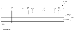
도 4를 참조하면, 표시 패널(DP)의 제2 서브 영역(SDA2)은 베이스 기판(BS) 및 베이스 기판(BS) 상에 구비된 표시 소자층(DEL)을 포함한다. 표시 소자층(DEL)의 제2 서브 영역(SDA2)은 내부광을 발광하는 발광층을 포함할 수 있다. 발광층은 발광 영역(EA)에 대응하여 구비된다. 따라서, 표시 패널(DP)의 제2 서브 영역(SDA2)은 복수의 발광 영역(EA)을 통해서 이미지를 표시할 수 있다. 또한, 표시 패널(DP)의 제2 서브 영역(SDA2)은 투과 영역(TA)을 통해서 외광을 투과시킬 수 있다. 따라서, 표시 패널(DP)의 제2 서브 영역(SDA2)은 발광 영역(EA)을 통해 이미지를 표시하면서, 후방에 배치된 발광 모듈(LM) 및 카메라 모듈(CMM)이 외부 피사체를 감지하거나 출력된 광 신호를 외부에 용이하게 제공할 수 있게 한다.Referring to FIG. 4 , the second sub-area SDA2 of the display panel DP includes a base substrate BS and a display element layer DEL provided on the base substrate BS. The second sub-area SDA2 of the display element layer DEL may include a light-emitting layer that emits internal light. The light emitting layer is provided to correspond to the light emitting area (EA). Accordingly, the second sub-area SDA2 of the display panel DP can display an image through a plurality of light-emitting areas EA. Additionally, the second sub-area SDA2 of the display panel DP may transmit external light through the transmission area TA. Accordingly, the second sub-area (SDA2) of the display panel (DP) displays an image through the light-emitting area (EA), while the light-emitting module (LM) and camera module (CMM) disposed at the rear detect or output an external subject. It is possible to easily provide an optical signal to the outside.
발광 영역(EA)에 대응하여 표시 소자층(DEL)에는 각종 소자들 및 배선들이 구비되어 발광 영역(EA)으로 입사된 외광의 투과율이 지극히 낮거나 거의 투과되지 못한다. 그러나, 투과 영역(TA)에 대응하여 표시 소자층(DEL)에는 각종 소자들 및 배선들이 구비되지 않아 외광의 투과율을 향상시킬 수 있다.In response to the light emitting area EA, the display element layer DEL is provided with various elements and wires, so that the transmittance of external light incident on the light emitting area EA is extremely low or barely transmitted. However, since various elements and wires are not provided in the display element layer (DEL) corresponding to the transmission area (TA), the transmittance of external light can be improved.
도 4에서는 발광 영역(EA)과 바로 인접하여 투과 영역(TA)이 구비되는 구조로 도시되었으나, 발광 영역(EA)과 투과 영역(TA) 사이에는 비발광 영역이 더 구비될 수 있다.In FIG. 4 , a structure is shown in which a transmissive area (TA) is immediately adjacent to the emissive area (EA), but a non-emissive area may be further provided between the emissive area (EA) and the transmissive area (TA).
도 5는 본 발명의 도 3에 도시된 표시 패널의 제2 서브 영역의 화소 구조를 나타낸 평면도이다.FIG. 5 is a plan view showing the pixel structure of the second sub-region of the display panel shown in FIG. 3 of the present invention.
도 5를 참조하면, 표시 패널(DP)의 제2 서브 영역(SDA2)은 복수의 화소를 포함할 수 있다. 복수의 화소들 각각은 발광 영역(EA), 비발광 영역(NEA) 및 투과 영역(TA)을 포함할 수 있다. 도 5에서는 복수의 화소들 중 인접하는 두 개의 화소(PXa, PXb)를 도시하였다. 실질적으로 두 개의 화소(PXa, PXb)는 동일한 구조로 이루어질 수 있다. 또한, 복수의 화소들은 서로 동일한 구조로 이루어질 수 있다.Referring to FIG. 5 , the second sub-area SDA2 of the display panel DP may include a plurality of pixels. Each of the plurality of pixels may include an emission area (EA), a non-emission area (NEA), and a transmission area (TA). Figure 5 shows two adjacent pixels (PXa, PXb) among a plurality of pixels. Substantially, the two pixels (PXa, PXb) may have the same structure. Additionally, a plurality of pixels may have the same structure.
각 화소(PXa, PXb)는 복수의 서브 화소를 포함할 수 있다. 발광 영역(EA)은 복수의 서브 화소에 각각 대응하는 복수의 발광 영역(EA1, EA2, EA3)을 포함한다. 투과 영역(TA)은 복수의 발광 영역(EA1, EA2, EA3)에 인접하여 배치된다. Each pixel (PXa, PXb) may include a plurality of sub-pixels. The light-emitting area EA includes a plurality of light-emitting areas EA1, EA2, and EA3, each corresponding to a plurality of sub-pixels. The transmission area TA is disposed adjacent to the plurality of light emitting areas EA1, EA2, and EA3.
본 발명의 일 예로, 도 5에 도시된 바와 같이, 각 화소는 레드 컬러(R)를 표시하는 제1 서브 화소, 그린 컬러(G)를 표시하는 제2 서브 화소 및 블루 컬러(B)를 표시하는 제3 서브 화소를 포함할 수 있다. 제1 내지 제3 서브 화소들은 동일한 사이즈를 가질 수 있거나 적어도 하나가 다른 사이즈를 가질 수 있다. 도 5에서와 같이 제3 서브 화소는 제1 및 제2 서브 화소들보다 큰 사이즈를 가질 수 있다. 이 경우, 제3 서브 화소에 대응하는 제3 발광 영역(EA3)은 제1 및 제2 서브 화소에 대응하는 제1 및 제2 발광 영역(EA1, EA2)보다 큰 사이즈를 가질 수 있다. As an example of the present invention, as shown in FIG. 5, each pixel displays a first sub-pixel displaying a red color (R), a second sub-pixel displaying a green color (G), and a blue color (B). may include a third sub-pixel. The first to third sub-pixels may have the same size or at least one of them may have a different size. As shown in FIG. 5, the third sub-pixel may have a larger size than the first and second sub-pixels. In this case, the third emission area EA3 corresponding to the third sub-pixel may have a larger size than the first and second emission areas EA1 and EA2 corresponding to the first and second sub-pixels.
투과 영역(TA)은 제1 내지 제3 서브 화소 각각의 사이즈의 합보다 큰 사이즈를 가질 수 있다. 그러나, 투과 영역(TA)의 크기는 이에 한정되지 않으며, 표시 패널(DP)의 제2 서브 영역(SDA2)의 원하는 투과율에 따라서 투과 영역(TA)의 크기는 달라질 수 있다. The transmission area TA may have a size larger than the sum of the sizes of the first to third sub-pixels. However, the size of the transmissive area TA is not limited to this, and the size of the transmissive area TA may vary depending on the desired transmittance of the second sub-area SDA2 of the display panel DP.
도 5에서는 각 화소(PXa, PXb)가 하나의 투과 영역(TA)을 갖는 구조를 도시하였으나, 본 발명은 이에 한정되지 않는다. 즉, 각 화소(PXa, PXb)는 복수의 투과 영역(TA)을 가질 수 있다. 예를 들어, 각 화소는 제1 내지 제3 서브 화소에 각각 인접한 세 개의 투과 영역을 포함할 수도 있다.Although FIG. 5 illustrates a structure in which each pixel (PXa, PXb) has one transmission area (TA), the present invention is not limited to this. That is, each pixel (PXa, PXb) may have a plurality of transmission areas (TA). For example, each pixel may include three transmission areas adjacent to the first to third sub-pixels, respectively.
또한, 도 5에서는 각 발광 영역(EA1-EA3)이 제1 및 제2 방향(DR1, DR2)으로 정의된 사각 형상을 갖는 구조를 도시하였으나, 발광 영역들(EA1-EA3) 각각의 형상은 이에 한정되지 않는다. 예를 들어, 발광 영역들(EA1-EA3) 각각은 마름모 형상을 가질 수 있다. 투과 영역(TA) 역시 제1 및 제2 방향(DR1, DR2)으로 정의된 사각 형상을 갖는 구조로 도시되었으나, 발광 영역들(EA1-EA3) 각각의 형상에 따라 투과 영역(TA)의 형상도 달라질 수 있다.In addition, Figure 5 shows a structure in which each light-emitting area (EA1-EA3) has a square shape defined in the first and second directions (DR1 and DR2), but the shape of each light-emitting area (EA1-EA3) is It is not limited. For example, each of the light emitting areas EA1-EA3 may have a diamond shape. The transmission area TA is also shown as having a square shape defined in the first and second directions DR1 and DR2, but the shape of the transmission area TA also varies depending on the shape of each of the light-emitting areas EA1-EA3. It may vary.
도 4 내지 도 5에 도시된 표시 패널(DP)의 제2 서브 영역(SDA2)은 각 화소(PXa, PXb)가 투과 영역(TA)을 구비하는 구조를 도시하였으나, 본 발명은 이에 한정되지 않는다. 즉, 제2 서브 영역(SDA2) 중 일부 영역만이 투명 표시 영역으로 구현될 수도 있다. 즉, 전자 모듈(EM) 내 전자 소자들(LM, CMM)과 평면상에서 중첩하는 위치에 배치된 화소들만이 투과 영역(TA)을 구비할 수 있고, 전자 소자들(LM, CMM)과 평면상에서 중첩하지 않은 화소들은 투과 영역(TA)을 구비하지 않을 수 있다. 따라서, 제2 서브 영역(SDA2) 중 상기한 투명 표시 영역에서는 발광 영역(EA)을 통해 이미지를 표시함과 동시에 투과 영역(TA)을 통해 외부 사물 또는 외부 이미지를 시인할 수 있으나, 나머지 표시 영역에서는 발광 영역(EA)을 통해 이미지만을 표시할 수 있다.Although the second sub-area SDA2 of the display panel DP shown in FIGS. 4 and 5 has a structure in which each pixel PXa and PXb has a transparent area TA, the present invention is not limited to this. . That is, only a portion of the second sub-area SDA2 may be implemented as a transparent display area. That is, only pixels arranged in a position that overlaps the electronic elements (LM, CMM) in the electronic module (EM) on the plane can have a transmission area (TA), and the Pixels that do not overlap may not have a transmission area (TA). Accordingly, in the transparent display area of the second sub-area SDA2, an image can be displayed through the luminous area EA and external objects or images can be viewed through the transmissive area TA, but the remaining display area In , only images can be displayed through the luminous area (EA).
도 6a 및 도 6b는 도 5에 도시된 투명 표시 패널을 I-I'에 따라 절단하여 표시 소자층을 상세히 도시한 단면도이다.FIGS. 6A and 6B are cross-sectional views showing the display element layer in detail by cutting the transparent display panel shown in FIG. 5 along II'.
도 5, 도 6a 및 도 6b를 참조하면, 표시 패널(DP)은 베이스 기판(BS) 및 표시 소자층(DEL)을 포함하고, 표시 소자층(DEL)은 제1 내지 제5 절연층들(10, 20, 30, 40, 50), 발광층(EL) 및 봉지층(60)을 포함할 수 있다. 도시하지는 않았으나, 표시 소자층(DEL)은 터치 센서, 반사 방지층, 및 윈도우 중 적어도 하나를 더 포함할 수 있다.5, 6A, and 6B, the display panel DP includes a base substrate BS and a display element layer DEL, and the display element layer DEL includes first to fifth insulating layers ( 10, 20, 30, 40, 50), a light emitting layer (EL), and an
베이스 기판(BS)은 실리콘 기판, 플라스틱 기판, 유리 기판, 절연 필름, 또는 복수의 절연층들을 포함하는 적층 구조체일 수 있다.The base substrate BS may be a silicon substrate, a plastic substrate, a glass substrate, an insulating film, or a laminated structure including a plurality of insulating layers.
제1 절연층(10)은 배리어층(11) 및 버퍼층(12)을 포함한다. 배리어층(11) 및 버퍼층(12) 중 적어도 하나는 생략될 수도 있고, 복수의 층들이 적층된 구조를 가질 수도 있으며, 어느 하나의 실시예로 한정되지 않는다.The first insulating
회로 소자층(CL)은 각 서브 화소에 구비된 서브 화소 회로 및 서브 화소 회로에 연결된 복수의 신호 라인들(SL)을 포함할 수 있다. 서브 화소 회로는 복수의 트랜지스터들(TR) 및 커패시터를 포함할 수 있다. 도 6a에서는 하나의 트랜지스터(TR)를 예시적으로 도시하였으나, 트랜지스터(TR)의 구조 및 개수는 이에 한정되지 않는다.The circuit element layer CL may include a sub-pixel circuit provided in each sub-pixel and a plurality of signal lines SL connected to the sub-pixel circuit. The sub-pixel circuit may include a plurality of transistors TR and a capacitor. Although one transistor TR is shown as an example in FIG. 6A, the structure and number of transistors TR are not limited thereto.
트랜지스터(TR)는 제1 절연층(10) 상에 배치된다. 트랜지스터(TR)는 반도체층(SP), 제어 전극(CE), 입력 전극(IE), 및 출력 전극(OE)을 포함한다. 반도체층(SP)은 제1 절연층(10) 상에 배치된다. 반도체층(SP)은 반도체 물질을 포함할 수 있다. 제어 전극(CE)은 제2 절연층(20)을 사이에 두고 반도체층(SP)으로부터 이격된다. The transistor TR is disposed on the first insulating
반도체층(SP)은 배리어층(11) 상에 배치된다. 반도체층(SP)은 트랜지스터(TR)의 채널 영역으로 기능할 수 있다. 반도체층(SP)은 아몰퍼스 실리콘, 폴리 실리콘, 산화물 반도체에서 선택될 수 있다. The semiconductor layer SP is disposed on the
제2 절연층(20)은 반도체층(SP) 상에 배치될 수 있다. 제2 절연층(20)은 제어 전극(CE)을 반도체층(SP)과 절연시킬 수 있다. The second insulating
제어 전극(CE)은 제2 절연층(20) 상에 배치될 수 있다. 제어 전극(CE)은 반도체층(SP)에 중첩하게 배치될 수 있다. 신호 라인들(SL)을 구성하는 제1 도전층은 제어 전극(CE)과 동일한 층상에 배치될 수 있다. The control electrode CE may be disposed on the second insulating
제3 절연층(30)은 제어 전극(CE) 상에 배치된다. 제3 절연층(30)은 유기물 및/또는 무기물을 포함할 수 있으며, 단층 또는 적층 구조를 가질 수 있다. 제어 전극(CE)은 제어 전극(CE)과 입력 및 출력 전극들(IE. OE)을 전기적으로 절연시킨다. 층간 절연막(ILD)은 무기물질을 포함할 수 있다. The third insulating
입력 및 출력 전극들(IE, OE)은 제3 절연층(30) 상에 배치된다. 입력 및 출력 전극들(IE, OE)은 각각 제3 절연층(30)와 제2 절연층(20)에 제공된 제1 및 제2 콘택홀들(CH1, CH2)을 통해 반도체층(SP)에 전기적으로 연결될 수 있다. 신호 라인들(SL)을 구성하는 제2 도전층은 입력 및 출력 전극들(IE, OE)과 동일한 층상에 배치될 수 있다. Input and output electrodes IE and OE are disposed on the third insulating
본 발명의 실시예에서, 표시 패널(DP)의 제2 서브 영역(SDA2)은 제어 전극(CE)이 반도체층(SP) 상부에 배치된 탑-게이트 구조를 갖는 것을 예시적으로 설명하였으나, 다른 실시예에서, 제2 서브 영역(SDA2)은 제어 전극(CE)이 반도체층(SP) 하부에 배치된 바텀-게이트 구조를 가질 수 있다. 또한, 다른 실시예에 따른 제2 서브 영역(SDA2)에서 복수의 트랜지스터(TR) 중 일부 트랜지스터는 탑-게이트 구조를 갖고, 나머지 일부 트랜지스터는 바텀-게이트 구조를 가질 수 있다.In an embodiment of the present invention, the second sub-area SDA2 of the display panel DP has been described as having a top-gate structure in which the control electrode CE is disposed on the semiconductor layer SP. However, in other embodiments, In an embodiment, the second sub-area SDA2 may have a bottom-gate structure in which the control electrode CE is disposed below the semiconductor layer SP. Additionally, in the second sub-area SDA2 according to another embodiment, some of the transistors TR may have a top-gate structure, and some of the remaining transistors may have a bottom-gate structure.
제4 절연층(40)은 입력 및 출력 전극들(IE, OE) 상에 배치된다. 제4 절연층(40)은 평탄면을 제공할 수 있다. 제4 절연층(40)은 유기물질을 포함할 수 있다. 유기물질은 아크릴계 수지, 메타크릴계 수지, 폴리이소프렌, 비닐계 수지, 에폭시계 수지, 우레탄계 수지, 셀룰로오스계 수지, 실록산계 수지, 폴리이미드계 수지, 폴리아미드계 수지 및 페릴렌계 수지 중 적어도 어느 하나를 포함할 수 있다.The fourth insulating
표시 소자(OLED)는 복수의 서브 화소에 각각 구비되고, 대응하는 서브 화소 회로 또는 신호 라인들(SL)에 연결될 수 있다. 본 발명의 실시예에서 표시 소자(OLED)는 유기 발광 다이오드일 수 있다. 표시 소자(OLED)는 제1 전극(E1), 발광층(EL), 제2 전극(E2)을 포함한다.The display element OLED may be provided in each of a plurality of sub-pixels and connected to a corresponding sub-pixel circuit or signal lines SL. In an embodiment of the present invention, the display device (OLED) may be an organic light emitting diode. The display device (OLED) includes a first electrode (E1), a light emitting layer (EL), and a second electrode (E2).
제1 전극(E1)은 제4 절연층(40)을 관통하여 트랜지스터(TR)에 접속될 수 있다. 한편, 도시되지 않았으나, 표시 패널(DP)의 제2 서브 영역(SDA2)은 제1 전극(E1)과 트랜지스터(TR) 사이에 배치되는 별도의 연결 전극을 더 포함할 수도 있고, 이때, 제1 전극(E1)은 연결 전극을 통해 트랜지스터(TR)에 전기적으로 접속될 수 있다.The first electrode E1 may penetrate the fourth insulating
제5 절연층(50)은 제4 절연층(40) 상에 배치된다. 제5 절연층(50)은 유기물 및/또는 무기물을 포함할 수 있으며, 단층 또는 적층 구조를 가질 수 있다. 제5 절연층(50)에는 개구부가 정의될 수 있다. 개구부는 제1 전극(E1)의 적어도 일부를 노출시킨다. 제5 절연층(50)은 화소 정의막일 수 있다.The fifth insulating
발광층(EL)은 제1 전극(E1)과 제2 전극(E2) 사이에 배치된다. 발광층(EL)은 적어도 하나의 발광층을 포함할 수 있다. 예를 들어, 발광층(EL)은 적색, 녹색, 및 청색을 발광하는 물질들 중 적어도 어느 하나의 물질로 구성될 수 있으며, 형광 물질 또는 인광 물질을 포함할 수 있다. 발광층(EL)은 유기 발광 물질 또는 무기 발광 물질을 포함할 수 있다. 발광층(EL)은 제1 전극(E1) 및 제2 전극(E2) 사이의 전위 차이에 응답하여 광을 발광할 수 있다.The light emitting layer EL is disposed between the first electrode E1 and the second electrode E2. The light emitting layer EL may include at least one light emitting layer. For example, the light emitting layer EL may be made of at least one material that emits red, green, and blue light, and may include a fluorescent material or a phosphorescent material. The light emitting layer (EL) may include an organic light emitting material or an inorganic light emitting material. The light emitting layer EL may emit light in response to a potential difference between the first electrode E1 and the second electrode E2.
본 실시예에서, 발광층(EL)은 복수의 개구부들에 중첩하는 일체의 형상을 가진 층으로 도시되었다. 다만, 이는 예시적으로 도시한 것이고, 발광층(EL)은 각 개구부에 대응되는 복수의 패턴들로 제공될 수도 있으며, 어느 하나의 실시예로 한정되지 않는다.In this embodiment, the light emitting layer EL is shown as a layer with an integrated shape that overlaps a plurality of openings. However, this is shown as an example, and the light emitting layer EL may be provided with a plurality of patterns corresponding to each opening, and is not limited to any one embodiment.
한편, 발광층(EL)은 발광층 외에 전하 제어층을 더 포함할 수 있다. 전하 제어층은 전하의 이동을 제어하여 표시 소자(OLED)의 발광 효율 및 수명을 향상시킨다. 이때, 발광층(EL)은 정공 수송 물질, 정공 주입 물질, 전자 수송 물질, 전자 주입 물질 중 적어도 어느 하나를 포함할 수 있다.Meanwhile, the light emitting layer EL may further include a charge control layer in addition to the light emitting layer. The charge control layer controls the movement of charges to improve the luminous efficiency and lifespan of the display device (OLED). At this time, the light emitting layer EL may include at least one of a hole transport material, a hole injection material, an electron transport material, and an electron injection material.
제2 전극(E2)은 발광층(EL) 상에 배치된다. 제2 전극(E2)은 제1 전극(E1)과 대향될 수 있다. 제2 전극(E2)은 복수의 화소들에 공통적으로 제공될 수 있다. 화소들 각각에 배치된 각각의 표시 소자(OLED)는 제2 전극(E2)을 통해 공통의 전원 전압(이하, 제2 전원 전압)을 수신한다.The second electrode E2 is disposed on the light emitting layer EL. The second electrode E2 may face the first electrode E1. The second electrode E2 may be commonly provided to a plurality of pixels. Each display element (OLED) disposed in each pixel receives a common power supply voltage (hereinafter referred to as second power voltage) through the second electrode E2.
제2 전극(E2)은 투과형 도전 물질 또는 반 투과형 도전 물질을 포함할 수 있다. 이에 따라, 발광 패턴(EP)에서 생성된 광은 제2 전극(E2)을 통해 제3 방향(DR3)을 향해 용이하게 출사될 수 있다. 다만, 이는 예시적으로 도시한 것이고, 본 발명의 일 실시예에 따른 표시 소자(OLED)는 설계에 따라, 제1 전극(E1)이 투과형 또는 반 투과형 물질을 포함하는 배면 발광 방식으로 구동되거나, 전면과 배면 모두를 향해 발광하는 양면 발광 방식으로 구동될 수도 있으며, 어느 하나의 실시예로 한정되지 않는다.The second electrode E2 may include a transmissive conductive material or a semi-transmissive conductive material. Accordingly, the light generated in the emission pattern EP can be easily emitted toward the third direction DR3 through the second electrode E2. However, this is shown as an example, and the display element (OLED) according to an embodiment of the present invention is driven in a bottom-emitting manner in which the first electrode (E1) includes a transmissive or semi-transmissive material, depending on the design, or It may be driven in a double-sided light emission method that emits light toward both the front and back sides, and is not limited to any one embodiment.
봉지층(60)은 표시 소자(OLED) 상에 배치되어 표시 소자(OLED)를 봉지한다. 한편, 도시되지 않았으나, 제2 전극(E2)과 봉지층(60) 사이에는 제2 전극(E2)을 커버하는 캡핑층(capping layer)이 더 배치될 수도 있다. 봉지층(60)은 제3 방향(DR3)을 따라 순차적으로 적층된 적어도 하나의 무기층 및 적어도 하나의 유기층을 포함할 수 있다. The
도 5 및 도 6a에 도시된 바와 같이, 발광 영역(EA)과 투과 영역(TA) 사이에는 비발광 영역(NEA)이 정의되고, 비발광 영역(NEA)에는 화소 정의막인 제5 절연층(50)이 위치한다. As shown in FIGS. 5 and 6A, a non-emission area (NEA) is defined between the emission area (EA) and the transmission area (TA), and a fifth insulating layer (a pixel defining layer) is formed in the non-emission area (NEA). 50) is located.
도 6a에 도시된 바와 같이, 발광층(EL) 및 제2 전극(E2)은 투과 영역(TA)과 중첩하여 형성될 수 있다. 제2 전극(E2)이 투과형 또는 반투과형 전극으로 형성되는 경우, 제2 전극(E2)이 투과 영역(TA)과 중첩되더라도 화소들(PXa, PXb)이 배치된 영역에 비해 상대적으로 높은 투과율을 가진 투과 영역(TA)이 형성될 수 있다.As shown in FIG. 6A, the light emitting layer EL and the second electrode E2 may be formed to overlap the transmission area TA. When the second electrode E2 is formed as a transmissive or semi-transmissive electrode, even if the second electrode E2 overlaps the transmissive area TA, the transmittance is relatively high compared to the area where the pixels PXa and PXb are arranged. An excited transmission area (TA) may be formed.
도 6b에 도시된 바와 같이, 제1 전극(E1), 발광층(EL), 제2 전극(E2)은 투과 영역(TA)과 중첩하지 않는다. 즉, 제1 전극(E1), 발광층(EL), 제2 전극(E2)은 투과 영역(TA)에서 오픈된 구조로 형성될 수 있다. 특히, 제1 전극(E1), 발광층(EL), 제2 전극(E2) 중 제2 전극(E2)은 낮은 광 투과율을 갖기 때문에 제1 전극(E1), 발광층(EL), 제2 전극(E2)이 투과 영역(TA)에서 제거되므로 인해 표시 패널(DP)의 제2 서브 영역(SDA2)의 투과율이 개선될 수 있다. As shown in FIG. 6B, the first electrode E1, the light emitting layer EL, and the second electrode E2 do not overlap the transmission area TA. That is, the first electrode E1, the light emitting layer EL, and the second electrode E2 may be formed in an open structure in the transmission area TA. In particular, among the first electrode (E1), the light emitting layer (EL), and the second electrode (E2), the second electrode (E2) has a low light transmittance, so the first electrode (E1), the light emitting layer (EL), and the second electrode (E2) have low light transmittance. Since E2) is removed from the transmission area TA, the transmittance of the second sub-area SDA2 of the display panel DP may be improved.
다른 실시예에서, 발광층(EL)은 투과 영역(TA)과 중첩하여 형성되고, 제2 전극(E2)은 투과 영역(TA)과 중첩하지 않을 수 있다.In another embodiment, the light emitting layer EL may be formed to overlap the transmissive area TA, and the second electrode E2 may not overlap the transmissive area TA.
도 7은 본 발명의 일 실시예에 따른 표시 패널의 구동 영역들을 예시적으로 보여주는 도면이다.FIG. 7 is a diagram illustrating driving areas of a display panel according to an embodiment of the present invention.
도 7을 참조하면, 제1 표시 영역(DA1)은 제1 구동 영역(DDA1)을 포함하고, 제2 표시 영역(DA2)은 제2 구동 영역(DDA2), 제3 구동 영역(DDA3) 및 제4 구동 영역(DDA4)을 포함한다. 예시적인 실시예에서, 제1 표시 영역(DA1)은 1개의 구동 영역(DDA1)을 포함하고, 제2 표시 영역(DA2)이 3개의 구동 영역들(DDA2-DDA4)을 포함하나, 본 발명은 이에 한정되지 않는다. 즉, 제1 표시 영역(DA1)은 2개 이상의 구동 영역들을 포함할 수 있고, 제2 표시 영역(DA2)은 1개 이상의 구동 영역들을 포함할 수 있다. 또한, 도 7은 제1 내지 제4 구동 영역들(DDA1-DDA4)을 예시적으로 도시하나, 제1 내지 제4 구동 영역들(DDA1-DDA4)의 크기 및 형상은 다양하게 변경될 수 있다.Referring to FIG. 7, the first display area DA1 includes a first driving area DDA1, and the second display area DA2 includes a second driving area DDA2, a third driving area DDA3, and a third driving area DDA3. Contains 4 driving areas (DDA4). In an exemplary embodiment, the first display area DA1 includes one driving area DDA1 and the second display area DA2 includes three driving areas DDA2-DDA4. However, in the present invention, It is not limited to this. That is, the first display area DA1 may include two or more driving areas, and the second display area DA2 may include one or more driving areas. Additionally, FIG. 7 illustrates the first to fourth driving areas DDA1 to DDA4 by way of example, but the size and shape of the first to fourth driving areas DDA1 to DDA4 may vary.
도 8은 본 발명의 일 실시예에 따른 표시 패널 및 구동 회로를 포함하는 표시 유닛을 예시적으로 보여주는 블록도이다.Figure 8 is a block diagram illustrating a display unit including a display panel and a driving circuit according to an embodiment of the present invention.
도 8을 참조하면, 표시 유닛(DU)은 구동 회로(110) 및 표시 패널(DP)을 포함한다. 예시적인 실시예에서, 구동 회로(110)는 단일 칩 또는 복수의 칩들로 구현되어 도 1b에 도시된 메인 기판(MB) 상에 실장될 수 있다. 구동 회로(110)는 구동 컨트롤러(112) 및 데이터 드라이버(114)를 포함한다. 구동 컨트롤러(112)는 데이터 드라이버(114)로 데이터 제어 신호(DCS) 및 데이터 신호(DATA)를 제공하고, 제1 내지 제4 스캔 제어 신호들(FLM1-FLM4)을 표시 패널(DP)로 제공한다. 구동 컨트롤러(112)는 제1 내지 제4 스캔 제어 신호들(FLM1-FLM4)외에 다른 신호들(예를 들면, 적어도 하나의 클럭 신호)을 표시 패널(DP)로 더 제공할 수 있다.Referring to FIG. 8 , the display unit DU includes a
데이터 드라이버(114)는 데이터 제어 신호(DCS) 및 데이터 신호(DATA)에 응답해서 제1 데이터 라인들(DL11-DL1i), 제2 데이터 라인들(DL21-DL2j) 및 제3 데이터 라인들(DL31-DL3k)을 구동한다(여기서, i, j 및 k 각각은 양의 정수).The
표시 패널(DP)은 제1 내지 제4 구동 영역들(DDA1-DDA4)을 포함한다.The display panel DP includes first to fourth driving areas DDA1 to DDA4.
제1 구동 영역(DDA1)은 제1 스캔 드라이버(SD1) 및 제1 화소들(PX1)을 포함한다. 제1 화소들(PX1)은 제2 데이터 라인들(DL21-DL2j) 및 제1 스캔 라인들(SL11-SL1m)에 연결된다. 제1 스캔 드라이버(SD1)는 제1 스캔 제어 신호(FLM1)에 응답해서 제1 스캔 라인들(SL11-SL1m)을 구동한다(단, m은 양의 정수).The first driving area DDA1 includes a first scan driver SD1 and first pixels PX1. The first pixels (PX1) are connected to the second data lines (DL21-DL2j) and the first scan lines (SL11-SL1m). The first scan driver SD1 drives the first scan lines SL11-SL1m in response to the first scan control signal FLM1 (where m is a positive integer).
제2 구동 영역(DDA2)은 제2 스캔 드라이버(SD2) 및 제2 화소들(PX2)을 포함한다. 제2 화소들(PX2)은 제1 데이터 라인들(DL11-DL1i) 및 제2 스캔 라인들(SL21-SL2n)에 연결된다. 제2 스캔 드라이버(SD2)는 제2 스캔 제어 신호(FLM2)에 응답해서 제2 스캔 라인들(SL21-SL2n)을 구동한다(단, n은 양의 정수).The second driving area DDA2 includes a second scan driver SD2 and second pixels PX2. The second pixels PX2 are connected to the first data lines DL11-DL1i and the second scan lines SL21-SL2n. The second scan driver SD2 drives the second scan lines SL21-SL2n in response to the second scan control signal FLM2 (where n is a positive integer).
제3 구동 영역(DDA3)은 제3 스캔 드라이버(SD3) 및 제3 화소들(PX3)을 포함한다. 제3 화소들(PX3)은 제2 데이터 라인들(DL21-DL2j) 및 제3 스캔 라인들(SL31-SL3n)에 연결된다. 제3 스캔 드라이버(SD3)는 제3 스캔 제어 신호(FLM3)에 응답해서 제3 스캔 라인들(SL31-SL3n)을 구동한다.The third driving area DDA3 includes a third scan driver SD3 and third pixels PX3. The third pixels (PX3) are connected to the second data lines (DL21-DL2j) and the third scan lines (SL31-SL3n). The third scan driver SD3 drives the third scan lines SL31-SL3n in response to the third scan control signal FLM3.
제4 구동 영역(DDA4)은 제4 스캔 드라이버(SD4) 및 제4 화소들(PX4)을 포함한다. 제4 화소들(PX4)은 제3 데이터 라인들(DL31-DL3k) 및 제4 스캔 라인들(SL41-SL4n)에 연결된다. 제4 스캔 드라이버(SD4)는 제4 스캔 제어 신호(FLM4)에 응답해서 제4 스캔 라인들(SL41-SL4n)을 구동한다.The fourth driving area DDA4 includes a fourth scan driver SD4 and fourth pixels PX4. The fourth pixels PX4 are connected to the third data lines DL31-DL3k and the fourth scan lines SL41-SL4n. The fourth scan driver SD4 drives the fourth scan lines SL41-SL4n in response to the fourth scan control signal FLM4.
이와 같이, 제1 내지 제4 구동 영역들(DDA1-DDA4) 각각에 제1 내지 제4 스캔 드라이버들(SD1-SD4)을 구비하여 제1 내지 제4 구동 영역들(DDA1-DDA4)은 독립적으로 구동될 수 있다.In this way, each of the first to fourth driving areas DDA1 to DDA4 is provided with first to fourth scan drivers SD1 to SD4, so that the first to fourth driving areas DDA1 to DDA4 are independently operated. It can be driven.
예를 들어, 구동 컨트롤러(112)가 제1 스캔 제어 신호(FLM1)는 활성화하고, 제2 내지 제4 스캔 제어 신호들(FLM2-FLM4)은 비활성화하는 경우, 제1 스캔 드라이버(SD1)만 동작하여 제1 구동 영역(DDA1)에만 영상이 표시될 수 있다.For example, when the
도 9a는 본 발명의 예시적인 실시예에 따른 표시 패널의 동작을 설명하기 위한 도면이다. 도 9b는 본 발명의 예시적인 실시예에 따른 표시 패널의 동작을 설명하기 위한 타이밍도이다.FIG. 9A is a diagram for explaining the operation of a display panel according to an exemplary embodiment of the present invention. FIG. 9B is a timing diagram for explaining the operation of a display panel according to an exemplary embodiment of the present invention.
도 9a에는 표시 패널(DP)의 제1 내지 제4 구동 영역들(DDA1-DDA4) 중 제1 구동 영역(DDA1) 및 제3 구동 영역(DDA3)에는 영상(IM1)이 표시되고, 제2 구동 영역(DDA2) 및 제4 구동 영역(DDA4)은 오프 상태로 유지되는 것을 도시한다.In FIG. 9A , an image IM1 is displayed in the first driving area DDA1 and the third driving area DDA3 among the first to fourth driving areas DDA1 to DDA4 of the display panel DP, and the image IM1 is displayed in the second driving area DDA1 to DDA3 of the display panel DP. The area DDA2 and the fourth driving area DDA4 are shown to be maintained in an off state.
도 8, 도 9a 및 도 9b를 참조하면, 구동 컨트롤러(112)는 제1 스캔 제어 신호(FLM1) 및 제3 스캔 제어 신호(FLM3)은 활성화하고, 제2 스캔 제어 신호(FLM2) 및 제4 스캔 제어 신호(FLM4)을 비활성화한다. 또한 구동 컨트롤러(112)는 제1 구동 영역(DDA1) 및 제3 구동 영역(DDA3)에 표시될 영상(IM1)에 대응하는 데이터 신호(DATA) 및 데이터 제어 신호(DCS)를 데이터 드라이버(114)로 제공한다.Referring to FIGS. 8, 9A, and 9B, the
제1 스캔 드라이버(SD1) 및 제3 스캔 드라이버(SD3)는 각각 제1 스캔 제어 신호(FLM1) 및 제3 스캔 제어 신호(FLM3)에 응답해서 제1 스캔 라인들(SL11-SL1m) 및 제3 스캔 라인들(SL31-SL3n)을 구동한다. 데이터 드라이버(114)는 데이터 신호(DATA) 및 데이터 제어 신호(DCS)에 응답해서 제2 데이터 라인들(DL21-DL2j)을 구동한다.The first scan driver (SD1) and the third scan driver (SD3) are connected to the first scan lines (SL11-SL1m) and the third scan lines (SL11-SL1m) in response to the first scan control signal (FLM1) and the third scan control signal (FLM3), respectively. Drives the scan lines (SL31-SL3n). The
도 9b에 도시된 바와 같이, 제1 내지 제4 스캔 제어 신호들(FLM1-FLM4)은 한 프레임(FR)의 시작을 나타내는 신호일 수 있다. 예시적인 실시예에서, 제1 구동 영역(DDA1) 및 제3 구동 영역(DDA3)이 순차적으로 구동되도록 제1 스캔 제어 신호(FLM1) 및 제3 스캔 제어 신호(FLM3)는 순차적으로 활성 레벨(예를 들면, 하이 레벨)로 천이할 수 있다.As shown in FIG. 9B, the first to fourth scan control signals FLM1 to FLM4 may be signals indicating the start of one frame FR. In an exemplary embodiment, the first scan control signal FLM1 and the third scan control signal FLM3 are sequentially driven at an active level (e.g., For example, it can transition to a high level).
예시적인 실시예에서, 제2 구동 영역(DDA2) 및 제4 구동 영역(DDA4)을 오프 상태로 유지하기 위해 제2 스캔 제어 신호(FLM2) 및 제4 스캔 제어 신호(FLM4)는 비활성 레벨(예를 들면, 로우 레벨)로 유지될 수 있다.In an exemplary embodiment, the second scan control signal FLM2 and the fourth scan control signal FLM4 are set to an inactive level (e.g., For example, it may be maintained at a low level).
도 10a는 본 발명의 예시적인 실시예에 따른 표시 패널의 동작을 설명하기 위한 도면이다. 도 10b는 본 발명의 예시적인 실시예에 따른 표시 패널의 동작을 설명하기 위한 타이밍도이다.FIG. 10A is a diagram for explaining the operation of a display panel according to an exemplary embodiment of the present invention. FIG. 10B is a timing diagram for explaining the operation of a display panel according to an exemplary embodiment of the present invention.
도 10a에는 표시 패널(DP)의 제1 내지 제4 구동 영역들(DDA1-DDA4) 중 제2 내지 제4 구동 영역들(DDA2-DDA4)에는 영상(IM2)이 표시되고, 제1 구동 영역(DDA1) 은 오프 상태로 유지되는 것을 도시한다.In FIG. 10A , an image IM2 is displayed in the second to fourth driving areas DDA2 to DDA4 among the first to fourth driving areas DDA1 to DDA4 of the display panel DP, and the first driving area ( DDA1) is shown to remain in the off state.
도 8, 도 10a 및 도 10b를 참조하면, 구동 컨트롤러(112)는 제2 스캔 제어 신호(FLM2), 제3 스캔 제어 신호(FLM3) 및 제4 스캔 제어 신호(FLM4)은 활성화하고, 제1 스캔 제어 신호(FLM1)는 비활성화한다. 또한 구동 컨트롤러(112)는 제2 내지 제4 구동 영역들(DDA2-DDA4)에 표시될 영상(IM2)에 대응하는 데이터 신호(DATA) 및 데이터 제어 신호(DCS)를 데이터 드라이버(114)로 제공한다.Referring to FIGS. 8, 10A, and 10B, the
제2 스캔 드라이버(SD2), 제3 스캔 드라이버(SD3) 및 제4 스캔 드라이버(SD4)는 각각 제2 스캔 제어 신호(FLM2), 제3 스캔 제어 신호(FLM3) 및 제4 스캔 제어 신호(FLM4)에 응답해서 제2 스캔 라인들(SL21-SL2n), 제3 스캔 라인들(SL31-SL3n) 및 제4 스캔 라인들(SL41-SL4n)을 구동한다. 데이터 드라이버(114)는 데이터 신호(DATA) 및 데이터 제어 신호(DCS)에 응답해서 제1 데이터 라인들(DL11-DL1i), 제2 데이터 라인들(DL21-DL2j) 및 제3 데이터 라인들(DL31-DL3k)을 구동한다.The second scan driver (SD2), the third scan driver (SD3), and the fourth scan driver (SD4) are respectively connected to a second scan control signal (FLM2), a third scan control signal (FLM3), and a fourth scan control signal (FLM4). ), driving the second scan lines (SL21-SL2n), the third scan lines (SL31-SL3n), and the fourth scan lines (SL41-SL4n). The
도 10b에 도시된 바와 같이, 제1 내지 제4 스캔 제어 신호들(FLM1-FLM4)은 한 프레임(FR)의 시작을 나타내는 신호일 수 있다. 예시적인 실시예에서, 제2 구동 영역(DDA2), 제3 구동 영역(DDA3) 및 제4 구동 영역(DDA4)이 동시에 구동되도록 제2 스캔 제어 신호(FLM2), 제3 스캔 제어 신호(FLM3) 및 제4 스캔 제어 신호(FLM4)는 동시에 활성 레벨(예를 들면, 하이 레벨)로 천이할 수 있다.As shown in FIG. 10B, the first to fourth scan control signals FLM1 to FLM4 may be signals indicating the start of one frame FR. In an exemplary embodiment, the second scan control signal FLM2 and the third scan control signal FLM3 are used so that the second driving area DDA2, the third driving area DDA3, and the fourth driving area DDA4 are driven simultaneously. and the fourth scan control signal FLM4 may simultaneously transition to an active level (eg, high level).
예시적인 실시예에서, 제1 구동 영역(DDA1)을 오프 상태로 유지하기 위해 제1 스캔 제어 신호(FLM1)는 비활성 레벨(예를 들면, 로우 레벨)로 유지될 수 있다.In an exemplary embodiment, the first scan control signal FLM1 may be maintained at an inactive level (eg, low level) to maintain the first driving area DDA1 in an off state.
도 11은 본 발명의 일 실시예에 따른 표시 패널 및 구동 회로를 예시적으로 보여주는 블록도이다.Figure 11 is a block diagram illustrating a display panel and a driving circuit according to an embodiment of the present invention.
도 11을 참조하면, 표시 유닛(DU)은 제1 구동 회로(210), 제2 구동 회로(220) 및 표시 패널(DP)을 포함한다.Referring to FIG. 11 , the display unit DU includes a
제1 구동 회로(210)는 제1 구동 컨트롤러(212) 및 제1 데이터 드라이버(214)를 포함한다. 제1 구동 컨트롤러(212)는 제1 데이터 제어 신호(DCS1) 및 제1 데이터 신호(DATA1)를 제1 데이터 드라이버(214)로 제공하고, 제1 스캔 제어 신호(FLM1)를 표시 패널(DP)로 제공한다. 제1 구동 컨트롤러(212)는 제1 스캔 제어 신호(FLM1)외에 다른 신호들(예를 들면, 적어도 하나의 클럭 신호)을 표시 패널(DP)로 더 제공할 수 있다.The
제1 데이터 드라이버(214)는 제1 데이터 제어 신호(DCS1) 및 제1 데이터 신호(DATA1)에 응답해서 제2 데이터 라인들(DL21-DL2j) 을 구동한다.The
제2 구동 회로(220)는 제2 구동 컨트롤러(222) 및 제2 데이터 드라이버(224)를 포함한다. 제2 구동 컨트롤러(222)는 제2 데이터 제어 신호(DCS2) 및 제2 데이터 신호(DATA2)를 제2 데이터 드라이버(224)로 제공하고, 제2 내지 제4 스캔 제어 신호들(FLM2-FLM4)을 표시 패널(DP)로 제공한다. 제2 구동 컨트롤러(222)는 제2 내지 제4 스캔 제어 신호들(FLM2-FLM4)외에 다른 신호들(예를 들면, 적어도 하나의 클럭 신호)을 표시 패널(DP)로 더 제공할 수 있다.The
제2 데이터 드라이버(224)는 제2 데이터 제어 신호(DCS2) 및 제2 데이터 신호(DATA2)에 응답해서 제1 데이터 라인들(DL11-DL1i), 제3 데이터 라인들(DL31-DL3k) 및 제4 데이터 라인들(DL41-DL4j)을 구동한다.The
표시 패널(DP)은 제1 내지 제4 구동 영역들(DDA1-DDA4)을 포함한다.The display panel DP includes first to fourth driving areas DDA1 to DDA4.
제1 구동 영역(DDA1)은 제1 스캔 드라이버(SD1) 및 제1 화소들(PX1)을 포함한다. 제1 화소들(PX1)은 제2 데이터 라인들(DL21-DL2i) 및 제1 스캔 라인들(SL11-SL1m)에 연결된다. 제1 스캔 드라이버(SD1)는 제1 스캔 제어 신호(FLM1)에 응답해서 제1 스캔 라인들(SL11-SL1m)을 구동한다.The first driving area DDA1 includes a first scan driver SD1 and first pixels PX1. The first pixels (PX1) are connected to the second data lines (DL21-DL2i) and the first scan lines (SL11-SL1m). The first scan driver SD1 drives the first scan lines SL11-SL1m in response to the first scan control signal FLM1.
제2 구동 영역(DDA2)은 제2 스캔 드라이버(SD2) 및 제2 화소들(PX2)을 포함한다. 제2 화소들(PX2)은 제1 데이터 라인들(DL11-DL1i) 및 제2 스캔 라인들(SL21-SL2n)에 연결된다. 제2 스캔 드라이버(SD2)는 제2 스캔 제어 신호(FLM2)에 응답해서 제2 스캔 라인들(SL21-SL2n)을 구동한다.The second driving area DDA2 includes a second scan driver SD2 and second pixels PX2. The second pixels PX2 are connected to the first data lines DL11-DL1i and the second scan lines SL21-SL2n. The second scan driver SD2 drives the second scan lines SL21-SL2n in response to the second scan control signal FLM2.
제3 구동 영역(DDA3)은 제3 스캔 드라이버(SD3) 및 제3 화소들(PX3)을 포함한다. 제3 화소들(PX3)은 제4 데이터 라인들(DL41-DL4j) 및 제3 스캔 라인들(SL31-SL3n)에 연결된다. 제3 스캔 드라이버(SD3)는 제3 스캔 제어 신호(FLM3)에 응답해서 제3 스캔 라인들(SL31-SL3n)을 구동한다.The third driving area DDA3 includes a third scan driver SD3 and third pixels PX3. The third pixels (PX3) are connected to the fourth data lines (DL41-DL4j) and the third scan lines (SL31-SL3n). The third scan driver SD3 drives the third scan lines SL31-SL3n in response to the third scan control signal FLM3.
제4 구동 영역(DDA4)은 제4 스캔 드라이버(SD4) 및 제4 화소들(PX4)을 포함한다. 제4 화소들(PX4)은 제3 데이터 라인들(DL31-DL3k) 및 제4 스캔 라인들(SL41-SL4n)에 연결된다. 제4 스캔 드라이버(SD4)는 제4 스캔 제어 신호(FLM4)에 응답해서 제4 스캔 라인들(SL41-SL4n)을 구동한다.The fourth driving area DDA4 includes a fourth scan driver SD4 and fourth pixels PX4. The fourth pixels PX4 are connected to the third data lines DL31-DL3k and the fourth scan lines SL41-SL4n. The fourth scan driver SD4 drives the fourth scan lines SL41-SL4n in response to the fourth scan control signal FLM4.
이와 같이, 제1 내지 제4 구동 영역들(DDA1-DDA4) 각각에 제1 내지 제4 스캔 드라이버들(SD1-SD4)을 구비하여 제1 내지 제4 구동 영역들(DDA1-DDA4)은 독립적으로 구동될 수 있다.In this way, each of the first to fourth driving areas DDA1 to DDA4 is provided with first to fourth scan drivers SD1 to SD4, so that the first to fourth driving areas DDA1 to DDA4 are independently operated. It can be driven.
예를 들어, 제1 구동 컨트롤러(212)가 제1 스캔 제어 신호(FLM1)를 활성화하고, 제2 구동 컨트롤러(222)가 제2 내지 제4 스캔 제어 신호들(FLM2-FLM4)을 비활성화하는 경우, 제1 스캔 드라이버(SD1)만 동작하여 제1 구동 영역(DDA1)에만 영상이 표시될 수 있다.For example, when the
도 12a는 본 발명의 예시적인 실시예에 따른 표시 패널의 동작을 설명하기 위한 도면이다. 도 12b는 본 발명의 예시적인 실시예에 따른 표시 패널의 동작을 설명하기 위한 타이밍도이다.FIG. 12A is a diagram for explaining the operation of a display panel according to an exemplary embodiment of the present invention. FIG. 12B is a timing diagram for explaining the operation of a display panel according to an exemplary embodiment of the present invention.
도 12a에는 표시 패널(DP)의 제1 내지 제4 구동 영역들(DDA1-DDA4) 중 제1 구동 영역(DDA1)에 영상(IM3)이 표시되고, 제2 내지 제4 구동 영역들(DDA2-DDA4)은 오프 상태로 유지되는 것을 도시한다.In FIG. 12A , an image IM3 is displayed in the first driving area DDA1 among the first to fourth driving areas DDA1 to DDA4 of the display panel DP, and the image IM3 is displayed in the second to fourth driving areas DDA2 to DDA4 of the display panel DP. DDA4) is shown to remain in the off state.
도 11, 도 12a 및 도 12b를 참조하면, 제1 구동 컨트롤러(212)는 제1 스캔 제어 신호(FLM1)를 활성화하고, 또한 제1 구동 컨트롤러(212)는 제1 구동 영역(DDA1)에 표시될 영상(IM3)에 대응하는 제1 데이터 신호(DATA1) 및 제1 데이터 제어 신호(DCS1)를 제1 데이터 드라이버(214)로 제공한다.11, 12A, and 12B, the
제2 구동 컨트롤러(222)는 제2 내지 제4 스캔 제어 신호들(FLM2-LM4)을 비활성화한다. 또한 제2 구동 컨트롤러(222)는 제2 데이터 신호(DATA2) 및 제2 데이터 제어 신호(DCS2)를 제2 데이터 드라이버(224)로 제공하지 않는다.The
제1 스캔 드라이버(SD1)는 제1 스캔 제어 신호(FLM1)에 응답해서 제1 스캔 라인들(SL11-SL1m)을 구동한다. 제1 데이터 드라이버(214)는 제1 데이터 신호(DATA1) 및 제1 데이터 제어 신호(DCS1)에 응답해서 제2 데이터 라인들(DL21-DL2j)을 구동한다.The first scan driver SD1 drives the first scan lines SL11-SL1m in response to the first scan control signal FLM1. The
도 12b에 도시된 바와 같이, 제1 내지 제4 스캔 제어 신호들(FLM1-FLM4)은 한 프레임(FR)의 시작을 나타내는 신호일 수 있다. 예시적인 실시예에서, 제1 구동 영역(DDA1)이 구동되도록 제1 스캔 제어 신호(FLM1)는 매 프레임마다 활성 레벨(예를 들면, 하이 레벨)로 천이할 수 있다.As shown in FIG. 12B, the first to fourth scan control signals FLM1 to FLM4 may be signals indicating the start of one frame FR. In an exemplary embodiment, the first scan control signal FLM1 may transition to an active level (eg, a high level) every frame so that the first driving area DDA1 is driven.
예시적인 실시예에서, 제2 구동 영역(DDA2), 제3 구동 영역(DDA3) 및 제4 구동 영역(DDA4)을 오프 상태로 유지하기 위해 제2 스캔 제어 신호(FLM2), 제3 스캔 제어 신호(FLM3) 및 제4 스캔 제어 신호(FLM4)는 비활성 레벨(예를 들면, 로우 레벨)로 유지될 수 있다.In an exemplary embodiment, a second scan control signal FLM2, a third scan control signal to keep the second driving area DDA2, third driving area DDA3, and fourth driving area DDA4 in the off state. (FLM3) and the fourth scan control signal (FLM4) may be maintained at an inactive level (eg, low level).
도 13a 내지 도 13b 각각은 도 1a 및 도 1b에 도시된 표시 장치가 폴딩된 것을 예시적으로 도시한 도면들이다.FIGS. 13A and 13B are diagrams illustrating the folded display device shown in FIGS. 1A and 1B , respectively.
도 3, 도 13a 및 도 13b를 참조하면, 본 발명의 일 실시예에 따른 표시 장치(DD)는 표시 패널(DP)의 제1 표시 영역(DA1)에 대응하는 적어도 일부가 벤딩될 수 있다.Referring to FIGS. 3, 13A, and 13B, the display device DD according to an embodiment of the present invention may have at least a portion corresponding to the first display area DA1 of the display panel DP bent.
표시 패널(DP)의 제2 서브 영역(SDA2)에 대응하는 표시 장치(DD)의 소정 영역은 플렉서블하여 벤딩, 폴딩, 롤딩 등의 동작에 의해 형상 변형이 가능할 수 있다.A predetermined area of the display device DD corresponding to the second sub-area SDA2 of the display panel DP may be flexible and may be transformed in shape through operations such as bending, folding, or rolling.
표시 장치(DD)가 제1 벤딩축(BX1)을 기준으로 완전히 아웃-폴딩되는 제1 모드에서 표시 패널(DP)의 제1 표시 영역(DA1)에만 영상이 표시될 수 있다. 다른 실시예에서, 제1 모드에서 표시 패널(DP)의 제2 표시 영역(DA2)에만 영상이 표시될 수 있다.In the first mode in which the display device DD is completely out-folded with respect to the first bending axis BX1, an image may be displayed only in the first display area DA1 of the display panel DP. In another embodiment, an image may be displayed only in the second display area DA2 of the display panel DP in the first mode.
제1 벤딩축(BX1)은 제1 표시 영역(DA1)과 제2 표시 영역(DA2)이 서로 인접하는 위치에 대응할 수 있다.The first bending axis BX1 may correspond to a position where the first display area DA1 and the second display area DA2 are adjacent to each other.
도 14는 도 7에 도시된 표시 패널을 포함하는 표시 장치가 폴딩된 것을 예시적으로 도시한 도면이다.FIG. 14 is a diagram illustrating a folded display device including the display panel shown in FIG. 7 .
도 7 및 도 14를 참조하면, 본 발명의 일 실시예에 따른 표시 장치(DD)는 표시 패널(DP)의 제2 표시 영역(DA2)에 대응하는 적어도 일부가 벤딩될 수 있다.Referring to FIGS. 7 and 14 , in the display device DD according to an embodiment of the present invention, at least a portion corresponding to the second display area DA2 of the display panel DP may be bent.
표시 패널(DP)의 제2 구동 영역(DDA2)에 대응하는 표시 장치(DD)의 소정 영역은 플렉서블하여 벤딩, 폴딩, 롤딩 등의 동작에 의해 형상 변형이 가능할 수 있다.A predetermined area of the display device DD corresponding to the second driving area DDA2 of the display panel DP may be flexible and may be deformed in shape through operations such as bending, folding, or rolling.
표시 장치(DD)가 제2 벤딩축(BX2)을 기준으로 완전히 아웃-폴딩되는 제2 모드에서 표시 패널(DP)의 제1 구동 영역(DDA1), 제3 구동 영역(DDA3) 및 제4 구동 영역(DDA4)에만 영상이 표시될 수 있다. 다른 실시예에서, 제2 모드에서 표시 패널(DP)의 제2 구동 영역(DDA2)에만 영상이 표시될 수 있다.In the second mode in which the display device DD is completely out-folded with respect to the second bending axis BX2, the first driving area DDA1, third driving area DDA3, and fourth driving area of the display panel DP Images can be displayed only in area (DDA4). In another embodiment, an image may be displayed only in the second driving area DDA2 of the display panel DP in the second mode.
제2 벤딩축(BX2)은 제2 구동 영역(DDA2)과 제3 구동 영역(DDA3)이 서로 인접하는 위치에 대응할 수 있다.The second bending axis BX2 may correspond to a position where the second driving area DDA2 and the third driving area DDA3 are adjacent to each other.
도 15는 도 1a 및 도 1b에 도시된 표시 장치가 폴딩된 것을 예시적으로 도시한 도면이다.FIG. 15 is a diagram illustrating the folded display device shown in FIGS. 1A and 1B.
도 7 및 도 15를 참조하면, 본 발명의 일 실시예에 따른 표시 장치(DD)는 표시 패널(DP)의 제4 표시 영역(DA4)에 대응하는 적어도 일부가 벤딩될 수 있다.Referring to FIGS. 7 and 15 , in the display device DD according to an embodiment of the present invention, at least a portion corresponding to the fourth display area DA4 of the display panel DP may be bent.
표시 패널(DP)의 제4 구동 영역(DDA4)에 대응하는 표시 장치(DD)의 소정 영역은 플렉서블하여 벤딩, 폴딩, 롤딩 등의 동작에 의해 형상 변형이 가능할 수 있다.A predetermined area of the display device DD corresponding to the fourth driving area DDA4 of the display panel DP may be flexible and may be transformed in shape through operations such as bending, folding, or rolling.
표시 장치(DD)가 제3 벤딩축(BX3)을 기준으로 완전히 아웃-폴딩되는 제3 모드에서 표시 패널(DP)의 제1 구동 영역(DDA1), 제2 구동 영역(DDA2) 및 제3 구동 영역(DDA3)에만 영상이 표시될 수 있다. 다른 실시예에서, 제3 모드에서 표시 패널(DP)의 제4 구동 영역(DDA4)에만 영상이 표시될 수 있다.In the third mode in which the display device DD is completely out-folded with respect to the third bending axis BX3, the first driving area DDA1, the second driving area DDA2, and the third driving area of the display panel DP Images can be displayed only in area (DDA3). In another embodiment, an image may be displayed only in the fourth driving area DDA4 of the display panel DP in the third mode.
제3 벤딩축(BX3)은 제3 구동 영역(DDA3)과 제4 구동 영역(DDA4)이 서로 인접하는 위치에 대응할 수 있다.The third bending axis BX3 may correspond to a position where the third driving area DDA3 and the fourth driving area DDA4 are adjacent to each other.
도 16은 예시적인 실시예에 따른 표시 패널을 예시적으로 보여주는 평면도이다.16 is a plan view illustrating a display panel according to an exemplary embodiment.
도 16을 참조하면, 표시 패널(DP)은 액티브 영역(AA) 및 주변 영역(NAA)을 포함한다. 액티브 영역(AA)은 제1 표시 영역(DA11) 및 제2 표시 영역(DA12)을 포함한다. 제1 표시 영역(DA11)은 제2 표시 영역(DA12)보다 상대적으로 높은 광 투과율을 가질 수 있다. 제1 표시 영역(DA11)에는 제1 전자 모듈 영역(EMA1) 및 제2 전자 모듈 영역(EMA2)이 정의될 수 있다. 제1 전자 모듈 영역(EMA1) 및 제2 전자 모듈 영역(EMA2)의 배면에는 도 1b에 도시된 발광 모듈(LM) 및 카메라 모듈(CMM)이 배열된다. 높은 광 투과율을 갖는 제1 표시 영역(DA11)과 중첩하도록 배열된 발광 모듈(LM) 및 카메라 모듈(CMM)은 외부 피사체를 감지하거나 출력된 광 신호를 외부에 용이하게 제공할 수 있다.Referring to FIG. 16 , the display panel DP includes an active area (AA) and a peripheral area (NAA). The active area AA includes a first display area DA11 and a second display area DA12. The first display area DA11 may have a relatively higher light transmittance than the second display area DA12. A first electronic module area (EMA1) and a second electronic module area (EMA2) may be defined in the first display area (DA11). The light emitting module LM and camera module CMM shown in FIG. 1B are arranged on the rear surfaces of the first electronic module area EMA1 and the second electronic module area EMA2. The light emitting module LM and camera module CMM arranged to overlap the first display area DA11 having high light transmittance can detect an external subject or easily provide an output optical signal to the outside.
예시적인 실시예에서, 제1 전자 모듈 영역(EMA1) 및 제2 전자 모듈 영역(EMA2)이 제1 표시 영역(DA11)의 하부 영역에 배열되나 본 발명은 이에 한정되지 않는다. 도 16에 도시된 표시 패널(DP)에서, 제1 표시 영역(DA11) 전체가 높은 광 투과율을 가지므로 제1 전자 모듈 영역(EMA1) 및 제2 전자 모듈 영역(EMA2)은 제1 표시 영역(DA11) 내 임의의 위치에 배치될 수 있다.In an exemplary embodiment, the first electronic module area EMA1 and the second electronic module area EMA2 are arranged in a lower area of the first display area DA11, but the present invention is not limited thereto. In the display panel DP shown in FIG. 16, since the entire first display area DA11 has high light transmittance, the first electronic module area EMA1 and the second electronic module area EMA2 are the first display area (EMA1) and the second electronic module area EMA2. DA11) It can be placed in any location within.
도 17a는 표시 패널의 표시 영역들을 예시적으로 보여주는 평면도이다.FIG. 17A is a plan view exemplarily showing display areas of a display panel.
도 17a을 참조하면, 표시 패널(DP)은 직사각 형상을 갖는다. 표시 패널(DP)은 복합 영역(CDA) 및 제2 표시 영역(DA22)을 포함한다. 복합 영역(CDA)은 제1 표시 영역(DA21), 제1 투명 영역(TW1) 및 제2 투명 영역(TW2)을 포함한다. 도 17a에서, 제1 투명 영역(TW1) 및 제2 투명 영역(TW2)은 제1 표시 영역(DA21)의 일측 및 타측에 각각 인접하게 배열되나, 본 발명은 이에 한정되지 않는다.Referring to FIG. 17A , the display panel DP has a rectangular shape. The display panel DP includes a complex area CDA and a second display area DA22. The complex area CDA includes a first display area DA21, a first transparent area TW1, and a second transparent area TW2. In FIG. 17A , the first transparent area TW1 and the second transparent area TW2 are arranged adjacent to one side and the other side of the first display area DA21, respectively, but the present invention is not limited thereto.
도면에 도시되지 않았으나, 제1 표시 영역(DA21)의 일부 영역은 도 3에 도시된 바와 같이, 제2 표시 영역(DA22)보다 상대적으로 높은 광 투과율을 가질 수 있다. 제1 표시 영역(DA21)의 높은 광 투과율을 갖는 영역의 배면에는 도 1b에 도시된 발광 모듈(LM) 및 카메라 모듈(CMM)이 배열될 수 있다.Although not shown in the drawing, some areas of the first display area DA21 may have a relatively higher light transmittance than the second display area DA22, as shown in FIG. 3 . The light emitting module LM and camera module CMM shown in FIG. 1B may be arranged on the back of the area with high light transmittance of the first display area DA21.
제1 투명 영역(TW1) 및 제2 투명 영역(TW2)은 도 6에 도시된 베이스 기판(BS) 만을 포함하고, 표시 소자층(DEL)을 포함하지 않는다. 따라서 제1 투명 영역(TW1) 및 제2 투명 영역(TW2)은 실질적으로 투명할 수 있다. 직사각형 형상의 표시 패널(DP)에서 제1 표시 영역(DA21) 및 제2 표시 영역(DA22) 에만 영상들을 표시하고, 제1 투명 영역(TW1) 및 제2 투명 영역(TW2)에는 영상이 표시되지 않는다. 따라서 표시 패널(DP)을 직사각형으로 생산하되, 일부 영역에만 영상을 표시할 수 있다.The first transparent area TW1 and the second transparent area TW2 include only the base substrate BS shown in FIG. 6 and do not include the display element layer DEL. Accordingly, the first transparent area TW1 and the second transparent area TW2 may be substantially transparent. In the rectangular display panel DP, images are displayed only in the first display area DA21 and DA22, and images are not displayed in the first transparent area TW1 and the second transparent area TW2. No. Therefore, the display panel (DP) is produced in a rectangular shape, but images can be displayed only in some areas.
도 8에 도시된 구동 회로(110)는 동작 모드에 따라서 제1 표시 영역(DA21) 및 제2 표시 영역(DA22) 중 적어도 하나에 영상을 표시할 수 있다. 예를 들어, 구동 회로(110)는 제1 모드 동안 제1 표시 영역(DA21)에 영상(IM4)을 표시하고, 제2 표시 영역(DA22)에 영상(IM5)을 표시할 수 있다. 예시적인 실시예에서, 영상(IM4) 및 영상(IM5)는 서로 연관된 영상일 수 있다. 다른 실시예에서, 영상(IM4) 및 영상(IM5)는 서로 독립적인 영상일 수 있다.The driving
도 17b는 도 17a에 도시된 표시 패널의 동작을 설명하기 위한 도면이다. FIG. 17B is a diagram for explaining the operation of the display panel shown in FIG. 17A.
도 17b를 참조하면, 도 8에 도시된 구동 회로(110)는 제2 모드 동안 제2 표시 영역(DA22)에 영상(IM5)을 표시할 수 있다. 구동 회로(110)는 제2 모드 동안 제1 표시 영역(DA21)에 어떠한 영상도 표시하지 않는다. 다른 실시예에서, 구동 회로(110)는 제2 모드 동안 제1 표시 영역(DA21)에만 영상을 표시하고, 제2 표시 영역(DA22)에는 영상을 표시하지 않을 수 있다.Referring to FIG. 17B, the driving
도 17c는 도 17a에 도시된 표시 패널의 동작을 설명하기 위한 도면이다.FIG. 17C is a diagram for explaining the operation of the display panel shown in FIG. 17A.
도 17c를 참조하면, 제2 표시 영역(DA22)은 제1 구동 영역(BDA1), 제2 구동 영역(BDA2) 및 제3 구동 영역(BDA3)을 포함한다. 제2 표시 영역(DA22)이 포함하는 구동 영역들의 수는 다양하게 변경될 수 있다.Referring to FIG. 17C, the second display area DA22 includes a first driving area BDA1, a second driving area BDA2, and a third driving area BDA3. The number of driving areas included in the second display area DA22 may vary.
예시적인 실시예에서, 복합 영역(CDA) 내 제1 투명 영역(TW1) 및 제2 투명 영역(TW2)은 제2 표시 영역(DA22) 내 제1 구동 영역(BDA1) 및 제3 구동 영역(BDA3)에 각각 인접한다. 또한 복합 영역(CDA) 내 제1 표시 영역(DA21)은 제2 표시 영역(DA22) 내 제2 구동 영역(BDA2)에 인접한다.In an exemplary embodiment, the first transparent area (TW1) and the second transparent area (TW2) in the composite area (CDA) are the first driving area (BDA1) and the third driving area (BDA3) in the second display area (DA22). ) are adjacent to each other. Additionally, the first display area DA21 in the composite area CDA is adjacent to the second driving area BDA2 in the second display area DA22.
도 8에 도시된 구동 회로(110)는 제3 모드 동안 제1 표시 영역(DA21) 및 제2 구동 영역(BDA2)에 영상(IM6)을 표시할 수 있다. 이때, 제1 구동 영역(BDA1) 및 제3 구동 영역(BDA3)은 비동작 상태(오프 상태)로 유지될 수 있다.The driving
도 18a 내지 도 18d는 표시 패널을 예시적으로 보여주는 평면도들이다.FIGS. 18A to 18D are plan views exemplarily showing a display panel.
도 18a에 도시된 표시 패널(DP)은 십자 형상을 갖는다. 표시 패널(DP)은 액티브 영역(AA) 및 주변 영역(NAA)을 포함한다. 액티브 영역(AA)은 제1 표시 영역(DA31), 제2 표시 영역(DA32), 제3 표시 영역(DA33), 제4 표시 영역(DA34) 및 제5 표시 영역(DA35)을 포함한다. 제1 표시 영역(DA31)의 일부 영역에는 제1 전자 모듈 영역(EMA1) 및 제2 전자 모듈 영역(EMA2)이 정의될 수 있다. 제1 전자 모듈 영역(EMA1) 및 제2 전자 모듈 영역(EMA2)의 배면에는 도 1b에 도시된 발광 모듈(LM) 및 카메라 모듈(CMM)이 배열된다. 다른 실시예에서, 제1 전자 모듈 영역(EMA1) 및 제2 전자 모듈 영역(EMA2)은 제2 표시 영역(DA32), 제3 표시 영역(DA33), 제4 표시 영역(DA34) 및 제5 표시 영역(DA35) 중 어느 하나에 정의될 수 있다.The display panel DP shown in FIG. 18A has a cross shape. The display panel DP includes an active area (AA) and a peripheral area (NAA). The active area AA includes a first display area DA31, a second display area DA32, a third display area DA33, a fourth display area DA34, and a fifth display area DA35. A first electronic module area (EMA1) and a second electronic module area (EMA2) may be defined in a portion of the first display area (DA31). The light emitting module LM and camera module CMM shown in FIG. 1B are arranged on the rear surfaces of the first electronic module area EMA1 and the second electronic module area EMA2. In another embodiment, the first electronic module area (EMA1) and the second electronic module area (EMA2) include the second display area (DA32), the third display area (DA33), the fourth display area (DA34), and the fifth display area. It can be defined in any one of the areas (DA35).
도 18b에 도시된 표시 패널(DP)은 액티브 영역(AA) 및 주변 영역(NAA)을 포함한다. 액티브 영역(AA)은 제1 표시 영역(DA41), 제2 표시 영역(DA42) 및 제3 표시 영역(DA43)을 포함한다. 제1 표시 영역(DA41) 및 제2 표시 영역(DA42)은 제3 표시 영역(DA43)의 일측에 서로 이격되어 배치될 수 있다.The display panel DP shown in FIG. 18B includes an active area (AA) and a peripheral area (NAA). The active area AA includes a first display area DA41, a second display area DA42, and a third display area DA43. The first display area DA41 and the second display area DA42 may be arranged to be spaced apart from each other on one side of the third display area DA43.
제1 표시 영역(DA41)의 일부 영역에는 제1 전자 모듈 영역(EMA1) 및 제2 전자 모듈 영역(EMA2)이 정의될 수 있다. 제1 전자 모듈 영역(EMA1) 및 제2 전자 모듈 영역(EMA2)의 배면에는 도 1b에 도시된 발광 모듈(LM) 및 카메라 모듈(CMM)이 배열된다. 다른 실시예에서, 제1 전자 모듈 영역(EMA1) 및 제2 전자 모듈 영역(EMA2)은 제2 표시 영역(DA42) 및 제3 표시 영역(DA43) 중 어느 하나에 정의될 수 있다.A first electronic module area (EMA1) and a second electronic module area (EMA2) may be defined in a portion of the first display area (DA41). The light emitting module LM and camera module CMM shown in FIG. 1B are arranged on the rear surfaces of the first electronic module area EMA1 and the second electronic module area EMA2. In another embodiment, the first electronic module area EMA1 and the second electronic module area EMA2 may be defined in one of the second display area DA42 and the third display area DA43.
도 18c에 도시된 표시 패널(DP)은 액티브 영역(AA) 및 주변 영역(NAA)을 포함한다. 액티브 영역(AA)은 제1 표시 영역(DA51) 및 제2 표시 영역(DA52)을 포함한다. 제1 표시 영역(DA51)은 삼각 형상을 가지며, 제2 표시 영역(DA52)은 사각 형상을 갖는다.The display panel DP shown in FIG. 18C includes an active area (AA) and a peripheral area (NAA). The active area AA includes a first display area DA51 and a second display area DA52. The first display area DA51 has a triangular shape, and the second display area DA52 has a square shape.
제1 표시 영역(DA51)의 일부 영역에는 제1 전자 모듈 영역(EMA1) 및 제2 전자 모듈 영역(EMA2)이 정의될 수 있다. 제1 전자 모듈 영역(EMA1) 및 제2 전자 모듈 영역(EMA2)의 배면에는 도 1b에 도시된 발광 모듈(LM) 및 카메라 모듈(CMM)이 배열된다. 다른 실시예에서, 제1 전자 모듈 영역(EMA1) 및 제2 전자 모듈 영역(EMA2)은 제2 표시 영역(DA52)에 정의될 수 있다. A first electronic module area (EMA1) and a second electronic module area (EMA2) may be defined in a portion of the first display area (DA51). The light emitting module LM and camera module CMM shown in FIG. 1B are arranged on the rear surfaces of the first electronic module area EMA1 and the second electronic module area EMA2. In another embodiment, the first electronic module area EMA1 and the second electronic module area EMA2 may be defined in the second display area DA52.
도 18d에 도시된 표시 패널(DP)은 제1 내지 제3 표시면들(DS1, DS2, DS3)을 포함한다. 도면에 도시되지 않았으나, 표시 패널(DP)은 숨은 제4 내지 제 6 표시면들을 더 포함할 수 있다. 도 18d에 도시된 표시 패널(DP)은 6개의 표시면들을 갖는 육면체이나, 본 발명은 이에 한정되지 않는다. 예를 들어, 표시 패널(DP)은 4개의 표시면들을 갖는 사면체, 5개의 표시면들을 갖는 오면체와 같이 다양한 형상을 가질 수 있다.The display panel DP shown in FIG. 18D includes first to third display surfaces DS1, DS2, and DS3. Although not shown in the drawing, the display panel DP may further include hidden fourth to sixth display surfaces. The display panel DP shown in FIG. 18D is a hexahedron having six display surfaces, but the present invention is not limited thereto. For example, the display panel DP may have various shapes, such as a tetrahedron with four display surfaces or a pentahedron with five display surfaces.
제1 표시면(DS1)은 제1 액티브 영역(AA61) 및 제1 주변 영역(NAA61)을 포함한다. 제2 표시면(DS2)은 제2 액티브 영역(AA62) 및 제2 주변 영역(NAA62)을 포함한다. 제3 표시면(DS3)은 제3 액티브 영역(AA63) 및 제3 주변 영역(NAA63)을 포함한다.The first display surface DS1 includes a first active area AA61 and a first peripheral area NAA61. The second display surface DS2 includes a second active area AA62 and a second peripheral area NAA62. The third display surface DS3 includes a third active area AA63 and a third peripheral area NAA63.
제2 표시면(DS2)의 제2 액티브 영역(AA62)의 일부 영역에는 제1 전자 모듈 영역(EMA1) 및 제2 전자 모듈 영역(EMA2)이 정의될 수 있다. 제1 전자 모듈 영역(EMA1) 및 제2 전자 모듈 영역(EMA2)의 배면에는 도 1b에 도시된 발광 모듈(LM) 및 카메라 모듈(CMM)이 배열된다. 다른 실시예에서, 제1 전자 모듈 영역(EMA1) 및 제2 전자 모듈 영역(EMA2)은 제2 표시 영역(AA62)에 정의될 수 있다. A first electronic module area EMA1 and a second electronic module area EMA2 may be defined in a portion of the second active area AA62 of the second display surface DS2. The light emitting module LM and camera module CMM shown in FIG. 1B are arranged on the rear surfaces of the first electronic module area EMA1 and the second electronic module area EMA2. In another embodiment, the first electronic module area EMA1 and the second electronic module area EMA2 may be defined in the second display area AA62.
상술한 바와 같이, 본 발명의 표시 패널(DP)은 2개 이상의 표시 영역들을 포함할 수 있다. 2개 이상의 표시 영역들은 동시에 연관된 영상을 표시할 수 있고 또는 독립적으로 영상을 표시할 수 있다. 표시 패널(DP)에 구비되는 표시 영역들의 개수 및 형상은 다양하게 변경될 수 있다. 표시 영역들 중 적어도 하나는 상대적으로 높은 광 투과율을 가져서 배면에 배치된 전자 모듈들이 외부 피사체를 감지하거나 출력된 광 신호를 외부에 용이하게 제공할 수 있도록 한다. 표시 영역들 중 적어도 하나는 플렉서블하여 벤딩, 폴딩, 롤딩 등의 동작에 의해 형상 변형이 가능할 수 있다. As described above, the display panel DP of the present invention may include two or more display areas. Two or more display areas may display related images simultaneously or may display images independently. The number and shape of display areas provided on the display panel DP can be changed in various ways. At least one of the display areas has a relatively high light transmittance so that electronic modules disposed on the back can detect an external subject or easily provide an output optical signal to the outside. At least one of the display areas may be flexible so that its shape can be changed through operations such as bending, folding, or rolling.
이상 실시예를 참조하여 설명하였지만, 해당 기술 분야의 숙련된 당업자는 하기의 특허 청구의 범위에 기재된 본 발명의 사상 및 영역으로부터 벗어나지 않는 범위 내에서 본 발명을 다양하게 수정 및 변경시킬 수 있음을 이해할 수 있을 것이다. 또한 본 발명에 개시된 실시예는 본 발명의 기술 사상을 한정하기 위한 것이 아니고, 하기의 특허 청구의 범위 및 그와 동등한 범위 내에 있는 모든 기술 사상은 본 발명의 권리범위에 포함되는 것으로 해석되어야 할 것이다.Although the description has been made with reference to the above examples, those skilled in the art will understand that various modifications and changes can be made to the present invention without departing from the spirit and scope of the present invention as set forth in the claims below. You will be able to. In addition, the embodiments disclosed in the present invention are not intended to limit the technical idea of the present invention, and all technical ideas within the scope of the following patent claims and equivalents should be construed as being included in the scope of the present invention. .
ED: 전자 장치
DP: 표시 패널
WM: 윈도우 모듈
EDC: 외부 케이스
EM: 전자 모듈
LM: 발광 모듈
CMM: 카메라 모듈
110, 210: 제1 구동 회로
220: 제2 구동 회로
112, 212: 제1 구동 컨트롤러
222: 제2 구동 컨트롤러
114, 214: 제1 데이터 드라이버
224: 제2 데이터 드라이버ED: electronic device
DP: Display panel
WM: Windows module
EDC: External Case
EM: electronic module
LM: Light emitting module
CMM: Camera module
110, 210: first driving circuit
220: second driving circuit
112, 212: first drive controller
222: second drive controller
114, 214: first data driver
224: Second data driver
Claims (27)
제1 데이터 신호 및 제1 데이터 제어 신호를 제공하는 제1 구동 컨트롤러;
상기 제1 데이터 신호 및 상기 제1 데이터 제어 신호에 응답해서 상기 제1 표시 영역의 제1 데이터 라인들을 구동하는 제1 데이터 드라이버;
제2 데이터 신호 및 제2 데이터 제어 신호를 제공하는 제2 구동 컨트롤러; 및
상기 제2 데이터 신호 및 상기 제2 데이터 제어 신호에 응답해서 상기 제2 표시 영역의 제2 데이터 라인들을 구동하는 제2 데이터 드라이버를 포함하되,
상기 제1 표시 영역은 제1 서브 영역 및 제2 서브 영역을 포함하고,
상기 제2 서브 영역은 발광 영역 및 상기 발광 영역에 인접하고 외광이 투과되는 투과 영역을 포함하는 표시 장치.a display panel including a first display area having a first shape and a second display area having a second shape;
a first drive controller providing a first data signal and a first data control signal;
a first data driver driving first data lines of the first display area in response to the first data signal and the first data control signal;
a second drive controller providing a second data signal and a second data control signal; and
A second data driver driving second data lines of the second display area in response to the second data signal and the second data control signal,
The first display area includes a first sub-area and a second sub-area,
The second sub-area includes a light-emitting area and a transmission area adjacent to the light-emitting area through which external light passes.
상기 제2 서브 영역은 상기 제2 표시 영역과 인접하게 배치되는 표시 장치.According to claim 1,
The second sub-area is disposed adjacent to the second display area.
상기 표시 패널은,
베이스 기판;
상기 베이스 기판 상에 구비되는 회로 소자층;
상기 발광 영역에 대응하여 상기 회로 소자층 상에 구비된 제1 전극;
상기 발광 영역에 대응하여 상기 제1 전극 상에 구비된 발광층; 및
상기 발광층 상에 제공되는 제2 전극을 포함하는 표시 장치.According to claim 1,
The display panel is,
base substrate;
A circuit element layer provided on the base substrate;
a first electrode provided on the circuit element layer corresponding to the light emitting area;
a light emitting layer provided on the first electrode corresponding to the light emitting area; and
A display device including a second electrode provided on the light emitting layer.
상기 표시 패널은,
베이스 기판;
상기 베이스 기판 상에 구비되는 회로 소자층;
상기 발광 영역에 대응하여 상기 회로 소자층 상에 구비된 제1 전극;
상기 회로 소자층 상에 구비되어 상기 발광 영역 및 상기 투과 영역을 정의하는 화소 정의막;
상기 발광 영역에 대응하여 상기 제1 전극 상에 구비된 발광층; 및
상기 발광층 상에 제공되고, 상기 투과 영역에 대응하여 오픈된 구조를 갖는 제2 전극을 포함하는 표시 장치.According to claim 1,
The display panel is,
base substrate;
A circuit element layer provided on the base substrate;
a first electrode provided on the circuit element layer corresponding to the light emitting area;
a pixel defining layer provided on the circuit element layer to define the light emitting area and the transmission area;
a light emitting layer provided on the first electrode corresponding to the light emitting area; and
A display device including a second electrode provided on the light emitting layer and having an open structure corresponding to the transmission area.
상기 제1 표시 영역은 제1 구동 영역을 포함하고, 상기 제2 표시 영역은 제2 구동 영역 및 제3 구동 영역을 포함하며,
상기 제1 구동 영역은 복수의 제1 스캔 라인들을 구동하는 제1 스캔 드라이버 및 상기 복수의 제1 스캔 라인들에 각각 연결된 제1 화소들을 포함하고,
상기 제2 구동 영역은 복수의 제2 스캔 라인들을 구동하는 제2 스캔 드라이버 및 상기 복수의 제2 스캔 라인들에 각각 연결된 제2 화소들을 포함하고,
상기 제3 구동 영역은 복수의 제3 스캔 라인들을 구동하는 제3 스캔 드라이버 및 상기 복수의 제3 스캔 라인들에 각각 연결된 제3 화소들을 포함하는 표시 장치.According to claim 1,
The first display area includes a first driving area, and the second display area includes a second driving area and a third driving area,
The first driving area includes a first scan driver driving a plurality of first scan lines and first pixels each connected to the plurality of first scan lines,
The second driving area includes a second scan driver driving a plurality of second scan lines and second pixels each connected to the plurality of second scan lines,
The third driving area includes a third scan driver driving a plurality of third scan lines and third pixels respectively connected to the plurality of third scan lines.
상기 제1 화소들은 상기 제1 데이터 라인들 중 대응하는 어느 하나에 각각 연결되고,
상기 제2 화소들 및 상기 제3 화소들은 상기 제2 데이터 라인들 중 대응하는 어느 하나에 각각 연결되는 표시 장치.According to claim 5,
The first pixels are each connected to a corresponding one of the first data lines,
The second pixels and the third pixels are each connected to a corresponding one of the second data lines.
상기 제2 데이터 드라이버는 상기 제2 데이터 신호 및 상기 제2 데이터 제어 신호에 응답해서 제3 데이터 라인들을 더 구동하고,
상기 제1 화소들은 상기 제1 데이터 라인들 중 대응하는 어느 하나에 각각 연결되고,
상기 제2 화소들은 상기 제2 데이터 라인들 중 대응하는 어느 하나에 각각 연결되고, 그리고
상기 제3 화소들은 상기 제3 데이터 라인들 중 대응하는 어느 하나에 각각 연결되는 표시 장치.According to claim 6,
The second data driver further drives third data lines in response to the second data signal and the second data control signal,
The first pixels are each connected to a corresponding one of the first data lines,
The second pixels are each connected to a corresponding one of the second data lines, and
The third pixels are each connected to a corresponding one of the third data lines.
상기 제1 구동 컨트롤러는 제1 스캔 제어 신호를 더 출력하며,
상기 제1 스캔 드라이버는 상기 제1 스캔 제어 신호에 동기해서 동작하는 표시 장치.According to claim 10,
The first drive controller further outputs a first scan control signal,
The first scan driver operates in synchronization with the first scan control signal.
상기 제2 구동 컨트롤러는 제2 스캔 제어 신호 및 제3 스캔 제어 신호를 더 출력하며,
상기 제2 스캔 드라이버는 상기 제2 스캔 제어 신호에 동기해서 동작하고, 상기 제3 스캔 드라이버는 상기 제3 스캔 제어 신호에 동기해서 동작하는 표시 장치.According to claim 10,
The second drive controller further outputs a second scan control signal and a third scan control signal,
The second scan driver operates in synchronization with the second scan control signal, and the third scan driver operates in synchronization with the third scan control signal.
상기 제1 형상과 상기 제2 형상은 면적 및 형태 중 적어도 하나가 서로 다른 표시 장치.According to claim 1,
The first shape and the second shape are different from each other in at least one of area and shape.
상기 표시 패널에 중첩하는 전자 모듈을 더 포함하되,
상기 제2 서브 영역의 상기 투과 영역은 상기 전자 모듈과 중첩하는 표시 장치.According to claim 1,
Further comprising an electronic module overlapping the display panel,
The display device wherein the transparent area of the second sub-area overlaps the electronic module.
상기 제2 서브 영역은 상기 제2 표시 영역과 인접하게 배치되는 표시 장치.According to claim 14,
The second sub-area is disposed adjacent to the second display area.
상기 제1 데이터 신호 및 상기 제1 데이터 제어 신호에 응답해서 상기 제1 표시 영역의 제1 데이터 라인들을 구동하는 제1 데이터 드라이버;
제2 데이터 신호 및 제2 데이터 제어 신호를 제공하는 제2 구동 컨트롤러; 및
상기 제2 데이터 신호 및 상기 제2 데이터 제어 신호에 응답해서 상기 제2 표시 영역의 제2 데이터 라인들을 구동하는 제2 데이터 드라이버를 포함하되,
상기 표시 패널은 상기 제1 표시 영역 및 상기 제2 표시 영역이 서로 인접하는 위치에 대응하는 제1 벤딩축을 기준으로 벤딩하는 표시 장치.A display panel including a first display area having a first shape and a second display area having a second shape; A first driving controller providing a first data signal and a first data control signal;
a first data driver driving first data lines of the first display area in response to the first data signal and the first data control signal;
a second drive controller providing a second data signal and a second data control signal; and
A second data driver driving second data lines of the second display area in response to the second data signal and the second data control signal,
The display panel is bent based on a first bending axis corresponding to a position where the first display area and the second display area are adjacent to each other.
상기 제1 표시 영역은 제1 서브 영역 및 제2 서브 영역을 포함하고,
상기 제2 서브 영역은 발광 영역 및 상기 발광 영역에 인접하고 외광이 투과되는 투과 영역을 포함하되,
상기 제2 서브 영역은 상기 제2 표시 영역과 인접하게 배치되는 표시 장치.According to claim 19,
The first display area includes a first sub-area and a second sub-area,
The second sub-area includes a light-emitting area and a transmission area adjacent to the light-emitting area and through which external light is transmitted,
The second sub-area is disposed adjacent to the second display area.
상기 표시 패널이 상기 제1 벤딩축을 기준으로 벤딩할 때 상기 제1 표시 영역과 상기 제2 표시 영역 중 어느 하나에 영상이 표시되는 표시 장치.According to claim 19,
A display device in which an image is displayed in one of the first display area and the second display area when the display panel is bent about the first bending axis.
상기 제1 데이터 신호 및 상기 제1 데이터 제어 신호에 응답해서 상기 복합 영역의 제1 데이터 라인들을 구동하는 제1 데이터 드라이버;
제2 데이터 신호 및 제2 데이터 제어 신호를 제공하는 제2 구동 컨트롤러; 및
상기 제2 데이터 신호 및 상기 제2 데이터 제어 신호에 응답해서 상기 제2 표시 영역의 제2 데이터 라인들을 구동하는 제2 데이터 드라이버를 포함하되,
상기 복합 영역은 영상을 표시하는 제1 표시 영역 및 상기 영상을 표시하지 않는 적어도 하나의 투명 영역을 포함하는 표시 장치.A display panel including a composite area having a first shape and a second display area having a second shape; a first drive controller providing a first data signal and a first data control signal;
a first data driver driving first data lines of the complex area in response to the first data signal and the first data control signal;
a second drive controller providing a second data signal and a second data control signal; and
A second data driver driving second data lines of the second display area in response to the second data signal and the second data control signal,
The composite area includes a first display area that displays an image and at least one transparent area that does not display the image.
상기 제1 구동 컨트롤러 및 상기 제2 구동 컨트롤러는,
제1 모드동안 상기 제1 표시 영역 및 상기 제2 표시 영역 모두에 상기 영상이 표시되도록 제어하는 표시 장치.According to claim 23,
The first drive controller and the second drive controller,
A display device that controls the image to be displayed in both the first display area and the second display area during a first mode.
상기 제1 구동 컨트롤러 및 상기 제2 구동 컨트롤러는,
제2 모드동안 상기 제1 표시 영역 및 상기 제2 표시 영역 중 어느 하나에 상기 영상이 표시되도록 제어하는 표시 장치.According to claim 23,
The first drive controller and the second drive controller,
A display device that controls the image to be displayed in one of the first display area and the second display area during a second mode.
상기 제2 표시 영역은 제1 구동 영역 및 제2 구동 영역을 포함하며,
상기 제1 구동 컨트롤러 및 상기 제2 구동 컨트롤러는,
제3 모드동안 상기 제1 표시 영역 및 상기 제1 구동 영역과 상기 제2 구동 영역 중 적어도 하나에 상기 영상이 표시되도록 제어하는 표시 장치.According to claim 23,
The second display area includes a first driving area and a second driving area,
The first drive controller and the second drive controller,
A display device that controls the image to be displayed on at least one of the first display area, the first driving area, and the second driving area during a third mode.
상기 적어도 하나의 투명 영역은 상기 제1 구동 영역과 상기 제2 구동 영역 중 적어도 하나에 인접한 표시 장치.
According to claim 26,
The at least one transparent area is adjacent to at least one of the first driving area and the second driving area.
Priority Applications (3)
| Application Number | Priority Date | Filing Date | Title |
|---|---|---|---|
| KR1020190039436A KR102649236B1 (en) | 2019-04-04 | 2019-04-04 | Display device |
| US16/838,029 US11263996B2 (en) | 2019-04-04 | 2020-04-02 | Display device |
| CN202010258553.2A CN111798793A (en) | 2019-04-04 | 2020-04-03 | display device |
Applications Claiming Priority (1)
| Application Number | Priority Date | Filing Date | Title |
|---|---|---|---|
| KR1020190039436A KR102649236B1 (en) | 2019-04-04 | 2019-04-04 | Display device |
Publications (2)
| Publication Number | Publication Date |
|---|---|
| KR20200118285A KR20200118285A (en) | 2020-10-15 |
| KR102649236B1 true KR102649236B1 (en) | 2024-03-21 |
Family
ID=72661650
Family Applications (1)
| Application Number | Title | Priority Date | Filing Date |
|---|---|---|---|
| KR1020190039436A Active KR102649236B1 (en) | 2019-04-04 | 2019-04-04 | Display device |
Country Status (3)
| Country | Link |
|---|---|
| US (1) | US11263996B2 (en) |
| KR (1) | KR102649236B1 (en) |
| CN (1) | CN111798793A (en) |
Families Citing this family (12)
| Publication number | Priority date | Publication date | Assignee | Title |
|---|---|---|---|---|
| US12274114B2 (en) * | 2019-09-06 | 2025-04-08 | Sharp Kabushiki Kaisha | Display device including metal oxide nanoparticles for uniform and efficient lighting and method for producing same |
| KR102696650B1 (en) * | 2019-09-30 | 2024-08-22 | 삼성디스플레이 주식회사 | Electric apparatus |
| US12527166B2 (en) * | 2020-09-17 | 2026-01-13 | Sharp Kabushiki Kaisha | Display device having increased light-emitting regions and method for manufacturing said display device |
| CN112562600B (en) * | 2020-12-01 | 2021-12-03 | Tcl华星光电技术有限公司 | Display device and driving method thereof |
| JP2022097093A (en) * | 2020-12-18 | 2022-06-30 | ソニーセミコンダクタソリューションズ株式会社 | Semiconductor device |
| CN114882791B (en) * | 2021-02-05 | 2025-02-28 | 群创光电股份有限公司 | Transparent display device |
| CN113156692B (en) * | 2021-03-25 | 2022-09-06 | 厦门天马微电子有限公司 | Display panel and display device |
| CN113096550B (en) * | 2021-04-08 | 2023-01-03 | Oppo广东移动通信有限公司 | Display module assembly and display device |
| CN113488516B (en) * | 2021-06-28 | 2022-05-03 | 武汉华星光电半导体显示技术有限公司 | Display panel and display device |
| KR102910106B1 (en) * | 2021-08-03 | 2026-01-09 | 삼성디스플레이 주식회사 | Display device |
| CN116018010B (en) * | 2021-10-20 | 2026-02-03 | 京东方科技集团股份有限公司 | Display substrate and display device |
| KR20230151601A (en) * | 2022-04-25 | 2023-11-02 | 삼성디스플레이 주식회사 | Display device |
Family Cites Families (17)
| Publication number | Priority date | Publication date | Assignee | Title |
|---|---|---|---|---|
| JP3749405B2 (en) | 1999-07-21 | 2006-03-01 | 株式会社荏原製作所 | Unit type pump gate |
| US7540106B2 (en) | 2007-01-22 | 2009-06-02 | George Weiss | Convertible cube particularly usable for display of pictures, objects, images, messages, and illumination patterns |
| WO2008126250A1 (en) | 2007-03-30 | 2008-10-23 | Pioneer Corporation | Light emitting device |
| KR20120032659A (en) | 2010-09-29 | 2012-04-06 | 엘지전자 주식회사 | Mobile terminal and method for controlling display thereof |
| TWI490829B (en) * | 2013-01-11 | 2015-07-01 | 友達光電股份有限公司 | Display panel and display device |
| KR20150008995A (en) | 2013-07-04 | 2015-01-26 | 삼성디스플레이 주식회사 | Mobile device including a flexible display device |
| KR102243652B1 (en) | 2014-02-17 | 2021-04-23 | 엘지전자 주식회사 | Display device and method for controlling the same |
| KR102315687B1 (en) * | 2014-04-02 | 2021-10-22 | 삼성디스플레이 주식회사 | Display panel and display device and having the same |
| US10255863B2 (en) * | 2014-04-02 | 2019-04-09 | Samsung Display Co., Ltd. | Display panel having a first region, a second region, and a third region between the first and second regions and including a drive portion on the third region |
| US10109684B2 (en) * | 2014-07-28 | 2018-10-23 | Shanghai Tianma AM-OLED Co., Ltd. | Pixel element structure, array structure and display device |
| KR101744893B1 (en) | 2015-03-09 | 2017-06-09 | 김창곤 | Cross shape display device |
| KR102479918B1 (en) * | 2016-04-05 | 2022-12-22 | 삼성디스플레이 주식회사 | Display apparatus |
| KR20180000771A (en) * | 2016-06-23 | 2018-01-04 | 삼성디스플레이 주식회사 | Display apparatus |
| KR102729882B1 (en) * | 2016-12-30 | 2024-11-13 | 엘지디스플레이 주식회사 | Display panel and display device including the same |
| CN107622752B (en) * | 2017-09-08 | 2019-04-16 | 上海天马微电子有限公司 | OLED display panel, driving method thereof and display device |
| CN109300951B (en) * | 2018-09-30 | 2020-09-08 | 上海天马微电子有限公司 | Display panel, manufacturing method thereof and electronic equipment |
| CN109979981B (en) * | 2019-03-29 | 2021-05-14 | 上海天马微电子有限公司 | Display panel, manufacturing method thereof and display device |
-
2019
- 2019-04-04 KR KR1020190039436A patent/KR102649236B1/en active Active
-
2020
- 2020-04-02 US US16/838,029 patent/US11263996B2/en active Active
- 2020-04-03 CN CN202010258553.2A patent/CN111798793A/en active Pending
Also Published As
| Publication number | Publication date |
|---|---|
| CN111798793A (en) | 2020-10-20 |
| US11263996B2 (en) | 2022-03-01 |
| KR20200118285A (en) | 2020-10-15 |
| US20200320959A1 (en) | 2020-10-08 |
Similar Documents
| Publication | Publication Date | Title |
|---|---|---|
| KR102649236B1 (en) | Display device | |
| US11515385B2 (en) | Display panel and electronic device including the same | |
| US20200194730A1 (en) | Display device | |
| CN119694255A (en) | Display panel and electronic device with input sensing function | |
| JP2020034921A (en) | Display device and electronic equipment | |
| CN112750390B (en) | Display panel and display device | |
| CN115734667A (en) | Display device | |
| CN113937135A (en) | Display panel | |
| KR102883172B1 (en) | Display apharatus, manufacturing method thereof, and electronic device | |
| US12075677B2 (en) | Display panel and display device | |
| US11672144B2 (en) | Display device | |
| KR20230045655A (en) | Light emitting display device | |
| CN220307716U (en) | Display device | |
| US12120937B2 (en) | Electronic device | |
| KR20240153442A (en) | Display device | |
| KR102676590B1 (en) | Electronic apparatus | |
| KR102930757B1 (en) | Light emitting display device | |
| US12453248B2 (en) | Display device | |
| KR102959765B1 (en) | display panel and electric apparatus | |
| US20250107011A1 (en) | Electronic device | |
| CN116367645A (en) | Light emitting display device and method for manufacturing light emitting display device | |
| KR20230156203A (en) | Display device | |
| KR20240001795A (en) | Display panel and electric apparatus | |
| CN120529796A (en) | Display device | |
| JP2026026015A (en) | Display device and electronic device including the same |
Legal Events
| Date | Code | Title | Description |
|---|---|---|---|
| PA0109 | Patent application |
St.27 status event code: A-0-1-A10-A12-nap-PA0109 |
|
| PG1501 | Laying open of application |
St.27 status event code: A-1-1-Q10-Q12-nap-PG1501 |
|
| A201 | Request for examination | ||
| P11-X000 | Amendment of application requested |
St.27 status event code: A-2-2-P10-P11-nap-X000 |
|
| P13-X000 | Application amended |
St.27 status event code: A-2-2-P10-P13-nap-X000 |
|
| PA0201 | Request for examination |
St.27 status event code: A-1-2-D10-D11-exm-PA0201 |
|
| P22-X000 | Classification modified |
St.27 status event code: A-2-2-P10-P22-nap-X000 |
|
| P22-X000 | Classification modified |
St.27 status event code: A-2-2-P10-P22-nap-X000 |
|
| E902 | Notification of reason for refusal | ||
| PE0902 | Notice of grounds for rejection |
St.27 status event code: A-1-2-D10-D21-exm-PE0902 |
|
| E13-X000 | Pre-grant limitation requested |
St.27 status event code: A-2-3-E10-E13-lim-X000 |
|
| P11-X000 | Amendment of application requested |
St.27 status event code: A-2-2-P10-P11-nap-X000 |
|
| P13-X000 | Application amended |
St.27 status event code: A-2-2-P10-P13-nap-X000 |
|
| E701 | Decision to grant or registration of patent right | ||
| PE0701 | Decision of registration |
St.27 status event code: A-1-2-D10-D22-exm-PE0701 |
|
| P22-X000 | Classification modified |
St.27 status event code: A-2-2-P10-P22-nap-X000 |
|
| PR0701 | Registration of establishment |
St.27 status event code: A-2-4-F10-F11-exm-PR0701 |
|
| PR1002 | Payment of registration fee |
St.27 status event code: A-2-2-U10-U11-oth-PR1002 Fee payment year number: 1 |
|
| PG1601 | Publication of registration |
St.27 status event code: A-4-4-Q10-Q13-nap-PG1601 |
|
| P22-X000 | Classification modified |
St.27 status event code: A-4-4-P10-P22-nap-X000 |