KR102585764B1 - Touch display device and touch display panel - Google Patents
Touch display device and touch display panel Download PDFInfo
- Publication number
- KR102585764B1 KR102585764B1 KR1020160053478A KR20160053478A KR102585764B1 KR 102585764 B1 KR102585764 B1 KR 102585764B1 KR 1020160053478 A KR1020160053478 A KR 1020160053478A KR 20160053478 A KR20160053478 A KR 20160053478A KR 102585764 B1 KR102585764 B1 KR 102585764B1
- Authority
- KR
- South Korea
- Prior art keywords
- touch
- pixels
- driving
- display device
- pixel
- Prior art date
- Legal status (The legal status is an assumption and is not a legal conclusion. Google has not performed a legal analysis and makes no representation as to the accuracy of the status listed.)
- Active
Links
Images


Classifications
-
- G—PHYSICS
- G06—COMPUTING OR CALCULATING; COUNTING
- G06F—ELECTRIC DIGITAL DATA PROCESSING
- G06F3/00—Input arrangements for transferring data to be processed into a form capable of being handled by the computer; Output arrangements for transferring data from processing unit to output unit, e.g. interface arrangements
- G06F3/01—Input arrangements or combined input and output arrangements for interaction between user and computer
- G06F3/03—Arrangements for converting the position or the displacement of a member into a coded form
- G06F3/041—Digitisers, e.g. for touch screens or touch pads, characterised by the transducing means
- G06F3/044—Digitisers, e.g. for touch screens or touch pads, characterised by the transducing means by capacitive means
- G06F3/0443—Digitisers, e.g. for touch screens or touch pads, characterised by the transducing means by capacitive means using a single layer of sensing electrodes
-
- G—PHYSICS
- G06—COMPUTING OR CALCULATING; COUNTING
- G06F—ELECTRIC DIGITAL DATA PROCESSING
- G06F3/00—Input arrangements for transferring data to be processed into a form capable of being handled by the computer; Output arrangements for transferring data from processing unit to output unit, e.g. interface arrangements
- G06F3/01—Input arrangements or combined input and output arrangements for interaction between user and computer
- G06F3/03—Arrangements for converting the position or the displacement of a member into a coded form
- G06F3/041—Digitisers, e.g. for touch screens or touch pads, characterised by the transducing means
- G06F3/0412—Digitisers structurally integrated in a display
-
- G—PHYSICS
- G06—COMPUTING OR CALCULATING; COUNTING
- G06F—ELECTRIC DIGITAL DATA PROCESSING
- G06F3/00—Input arrangements for transferring data to be processed into a form capable of being handled by the computer; Output arrangements for transferring data from processing unit to output unit, e.g. interface arrangements
- G06F3/01—Input arrangements or combined input and output arrangements for interaction between user and computer
- G06F3/03—Arrangements for converting the position or the displacement of a member into a coded form
- G06F3/041—Digitisers, e.g. for touch screens or touch pads, characterised by the transducing means
- G06F3/044—Digitisers, e.g. for touch screens or touch pads, characterised by the transducing means by capacitive means
-
- G—PHYSICS
- G06—COMPUTING OR CALCULATING; COUNTING
- G06F—ELECTRIC DIGITAL DATA PROCESSING
- G06F3/00—Input arrangements for transferring data to be processed into a form capable of being handled by the computer; Output arrangements for transferring data from processing unit to output unit, e.g. interface arrangements
- G06F3/01—Input arrangements or combined input and output arrangements for interaction between user and computer
- G06F3/03—Arrangements for converting the position or the displacement of a member into a coded form
- G06F3/041—Digitisers, e.g. for touch screens or touch pads, characterised by the transducing means
- G06F3/0416—Control or interface arrangements specially adapted for digitisers
- G06F3/04166—Details of scanning methods, e.g. sampling time, grouping of sub areas or time sharing with display driving
-
- G—PHYSICS
- G06—COMPUTING OR CALCULATING; COUNTING
- G06F—ELECTRIC DIGITAL DATA PROCESSING
- G06F3/00—Input arrangements for transferring data to be processed into a form capable of being handled by the computer; Output arrangements for transferring data from processing unit to output unit, e.g. interface arrangements
- G06F3/01—Input arrangements or combined input and output arrangements for interaction between user and computer
- G06F3/03—Arrangements for converting the position or the displacement of a member into a coded form
- G06F3/041—Digitisers, e.g. for touch screens or touch pads, characterised by the transducing means
- G06F3/0416—Control or interface arrangements specially adapted for digitisers
- G06F3/0418—Control or interface arrangements specially adapted for digitisers for error correction or compensation, e.g. based on parallax, calibration or alignment
- G06F3/04184—Synchronisation with the driving of the display or the backlighting unit to avoid interferences generated internally
-
- G—PHYSICS
- G06—COMPUTING OR CALCULATING; COUNTING
- G06F—ELECTRIC DIGITAL DATA PROCESSING
- G06F2203/00—Indexing scheme relating to G06F3/00 - G06F3/048
- G06F2203/033—Indexing scheme relating to G06F3/033
- G06F2203/0339—Touch strips, e.g. orthogonal touch strips to control cursor movement or scrolling; single touch strip to adjust parameter or to implement a row of soft keys
-
- G—PHYSICS
- G06—COMPUTING OR CALCULATING; COUNTING
- G06F—ELECTRIC DIGITAL DATA PROCESSING
- G06F2203/00—Indexing scheme relating to G06F3/00 - G06F3/048
- G06F2203/041—Indexing scheme relating to G06F3/041 - G06F3/045
- G06F2203/04103—Manufacturing, i.e. details related to manufacturing processes specially suited for touch sensitive devices
-
- G—PHYSICS
- G06—COMPUTING OR CALCULATING; COUNTING
- G06F—ELECTRIC DIGITAL DATA PROCESSING
- G06F2203/00—Indexing scheme relating to G06F3/00 - G06F3/048
- G06F2203/041—Indexing scheme relating to G06F3/041 - G06F3/045
- G06F2203/04112—Electrode mesh in capacitive digitiser: electrode for touch sensing is formed of a mesh of very fine, normally metallic, interconnected lines that are almost invisible to see. This provides a quite large but transparent electrode surface, without need for ITO or similar transparent conductive material
Landscapes
- Engineering & Computer Science (AREA)
- General Engineering & Computer Science (AREA)
- Theoretical Computer Science (AREA)
- Human Computer Interaction (AREA)
- Physics & Mathematics (AREA)
- General Physics & Mathematics (AREA)
- Devices For Indicating Variable Information By Combining Individual Elements (AREA)
- Position Input By Displaying (AREA)
Abstract
본 실시예들은 디스플레이 패널에 배치된 다수의 더미 화소를 이용하여 터치 구동 회로와 다수의 터치 센서를 연결함으로써 사용자의 터치 인식이 가능한 터치 디스플레이 장치를 제공한다. 터치 배선 구현 시 다수의 더미 화소에 포함된 화소 전극 또는 소스 라인과 동일한 물질을 이용함으로써 터치 배선 구현을 위한 별도의 공정이 필요하지 않도록 하는 이점을 제공한다. 또한, 두 개의 화소마다 하나의 데이터 라인이 배치되는 화소 구조인 경우 데이터 라인이 배치되지 않는 영역에 소스 라인을 배치하고 터치 배선으로 이용함으로써, 화소 메탈을 이용하는 경우에 비해 터치 인식 가능 영역을 확장할 수 있도록 한다.The present embodiments provide a touch display device capable of recognizing a user's touch by connecting a touch driving circuit and a plurality of touch sensors using a plurality of dummy pixels disposed on a display panel. When implementing touch wiring, the same material as the pixel electrodes or source lines included in the multiple dummy pixels is used, providing the advantage of eliminating the need for a separate process for implementing touch wiring. In addition, in the case of a pixel structure in which one data line is arranged for every two pixels, the touch recognition area can be expanded compared to the case of using pixel metal by placing the source line in the area where the data line is not arranged and using it as a touch wire. make it possible
Description
본 실시예들은 사용자의 터치 인식이 가능한 터치 디스플레이 패널 및 장치에 관한 것이다.These embodiments relate to a touch display panel and device capable of recognizing a user's touch.
정보화 사회가 발전함에 따라 화상을 표시하기 위한 표시장치에 대한 요구가 다양한 형태로 증가하고 있으며, 액정 디스플레이 장치, 플라즈마 디스플레이 장치, 유기발광 디스플레이 장치 등의 다양한 타입의 디스플레이 장치가 활용되고 있다.As the information society develops, the demand for display devices for displaying images is increasing in various forms, and various types of display devices such as liquid crystal display devices, plasma display devices, and organic light emitting display devices are being used.
이러한 디스플레이 장치들은 사용자에게 편의와 다양한 기능을 제공하기 위하여 최근 터치 기반의 입력 방식을 제공하고 있다.These display devices have recently been providing touch-based input methods to provide convenience and various functions to users.
이러한 터치 기반의 입력 방식을 제공하기 위해서는, 사용자의 터치 유무를 파악하고 터치 위치(터치 좌표)를 정확하게 검출할 수 있어야 한다.In order to provide such a touch-based input method, it is necessary to determine the presence or absence of a user's touch and accurately detect the touch location (touch coordinates).
이를 위해, 일 예로, 터치 디스플레이 패널에 배열된 다수의 터치 센서(터치 전극)을 통해 터치 센서 간의 캐패시턴스 또는 터치 센서와 포인터(예: 손가락 등) 간의 캐패시턴스의 변화를 토대로 터치 유무 및 터치 위치(터치 좌표) 등을 검출하는 방식이 많이 이용되고 있다.For this purpose, as an example, the presence or absence of touch and the touch position (touch location) are determined based on the change in capacitance between touch sensors or the capacitance between a touch sensor and a pointer (e.g., finger, etc.) through a plurality of touch sensors (touch electrodes) arranged on a touch display panel. Coordinates) detection methods are widely used.
하지만, 이러한 터치 기반의 입력 방식을 제공하기 위해서는, 터치 센서와 연결되는 터치 배선을 별도로 설계해야 하며, 터치 배선 설계 시 디스플레이 패널 내 존재하는 다른 배선과의 RC 로드나 디스플레이 저해 인자 등을 고려하여 설계가 이루어져야 한다.However, in order to provide this touch-based input method, the touch wire connected to the touch sensor must be designed separately, and when designing the touch wire, the RC load with other wires present in the display panel or display interference factors are taken into consideration. must be done.
특히, 대면적 디스플레이 패널에서 터치 기반의 입력 방식을 제공하는 경우 터치 배선 및 터치 센서 수에 따른 비용 증가, 터치 배선 설계의 어려움 등이 존재하여 터치 기반의 입력 방식을 대면적 디스플레이에 적용하기에는 한계가 존재한다.In particular, when providing a touch-based input method on a large-area display panel, there are limitations in applying the touch-based input method to a large-area display due to increased costs due to the number of touch wiring and touch sensors and difficulties in designing the touch wiring. exist.
본 실시예들의 목적은, 사용자의 터치 인식이 가능한 터치 디스플레이 패널과 터치 디스플레이 장치를 제공하는 데 있다.The purpose of the present embodiments is to provide a touch display panel and a touch display device capable of recognizing a user's touch.
본 실시예들의 목적은, 사용자의 터치 유무와 드래그 터치를 인식할 수 있는 터치 디스플레이 패널과 터치 디스플레이 장치를 제공하는 데 있다.The purpose of the present embodiments is to provide a touch display panel and a touch display device that can recognize the presence or absence of a user's touch and a drag touch.
본 실시예들의 목적은, 디스플레이 패널 내 배치된 다른 배선과의 RC 로드를 저감시키며 터치 배선이 설계된 터치 디스플레이 패널과 터치 디스플레이 장치를 제공하는 데 있다.The purpose of the present embodiments is to provide a touch display panel and a touch display device in which touch wiring is designed to reduce RC load with other wiring arranged in the display panel.
본 실시예들의 목적은, 대면적 디스플레이 패널에서 사용자의 터치 인식이 가능한 터치 디스플레이 패널과 터치 디스플레이 장치를 제공하는 데 있다.The purpose of the present embodiments is to provide a touch display panel and a touch display device capable of recognizing a user's touch on a large-area display panel.
일 실시예는, 다수의 구동 화소가 배치된 표시 영역과 다수의 전극 패턴이 배치된 비표시 영역을 포함하는 디스플레이 패널과, 표시 영역에 배치된 다수의 터치 센서와, 다수의 터치 센서를 구동하는 터치 구동 회로를 포함하는 터치 디스플레이 장치를 제공한다.One embodiment includes a display panel including a display area where a plurality of driving pixels are arranged and a non-display area where a plurality of electrode patterns are arranged, a plurality of touch sensors arranged in the display area, and a device that drives the plurality of touch sensors. A touch display device including a touch driving circuit is provided.
여기서, 비표시 영역에 배치되는 다수의 전극 패턴은 더미 화소일 수 있다.Here, a plurality of electrode patterns disposed in the non-display area may be dummy pixels.
이러한 터치 디스플레이 장치에서, 터치 구동 회로는 비표시 영역에 배치된 다수의 더미 화소를 통해 표시 영역에 배치된 다수의 터치 센서와 전기적으로 연결될 수 있다.In such a touch display device, the touch driving circuit may be electrically connected to a plurality of touch sensors arranged in the display area through a plurality of dummy pixels arranged in the non-display area.
여기서, 다수의 더미 화소는, 동일한 터치 센서와 전기적으로 연결된 더미 화소끼리 서로 전기적으로 연결되고, 다른 터치 센서와 전기적으로 연결된 더미 화소와는 이격되어 배치될 수 있다.Here, the plurality of dummy pixels may be arranged so that dummy pixels electrically connected to the same touch sensor are electrically connected to each other, and are spaced apart from dummy pixels electrically connected to other touch sensors.
즉, 더미 화소와 연결되는 터치 센서의 폭에 대응하는 단위로 분리되어 더미 화소끼리 연결된 상태일 수 있다.That is, the dummy pixels may be separated into units corresponding to the width of the touch sensor connected to the dummy pixels and connected to each other.
그리고, 다수의 터치 센서는, 표시 영역에서 비표시 영역에 인접한 일부 영역에 서로 이격되어 일렬로 배치될 수 있다.Additionally, a plurality of touch sensors may be arranged in a row and spaced apart from each other in a portion of the display area adjacent to the non-display area.
터치 구동 회로와 다수의 터치 센서를 전기적으로 연결하기 위하여, 일 예로, 터치 구동 회로와 비표시 영역에 배치된 다수의 더미 화소를 전기적으로 연결하는 제1연결부를 포함할 수 있다. 또한, 다수의 더미 화소와 표시 영역에 배치된 다수의 터치 센서를 전기적으로 연결하는 제2연결부를 포함할 수 있다.In order to electrically connect the touch driving circuit and the plurality of touch sensors, for example, it may include a first connection part that electrically connects the touch driving circuit and the plurality of dummy pixels disposed in the non-display area. Additionally, it may include a second connector that electrically connects a plurality of dummy pixels and a plurality of touch sensors arranged in the display area.
이때, 제1연결부와 제2연결부는, 다수의 더미 화소에 포함된 화소 전극을 구성하는 물질과 동일한 물질로 이루어질 수 있다.At this time, the first connection part and the second connection part may be made of the same material as the material constituting the pixel electrodes included in the plurality of dummy pixels.
또는, 제1연결부와 제2연결부는, 다수의 더미 화소에 포함된 소스 라인을 구성하는 물질과 동일한 물질로 이루어질 수 있다.Alternatively, the first connection part and the second connection part may be made of the same material as the material constituting the source lines included in the plurality of dummy pixels.
또는, 제1연결부와 제2연결부는, 다수의 더미 화소에 포함된 화소 전극이나 소스 라인이 배치된 층과 다른 층에 위치하는 신호 라인일 수도 있다.Alternatively, the first connection part and the second connection part may be a signal line located on a different layer from the layer on which the pixel electrodes or source lines included in the plurality of dummy pixels are disposed.
그리고, 다수의 더미 화소와 다수의 터치 센서를 전기적으로 연결하는 제2연결부는, 다수의 구동 화소에 포함된 화소 메탈, 소스 라인 또는 화소 전극이나 소스 라인이 배치된 층과 다른 층에 위치하는 신호 라인을 통해 다수의 터치 센서와 전기적으로 연결될 수 있다.And, the second connection part that electrically connects the plurality of dummy pixels and the plurality of touch sensors is a signal located in a different layer from the pixel metal, source line, or pixel electrode or source line included in the plurality of driving pixels. It can be electrically connected to multiple touch sensors through a line.
터치 구동 회로는, 한 프레임 구간 중 블랭크 구간 동안 다수의 터치 센서를 구동하는 터치 구동 신호를 출력할 수도 있고, 하나의 프레임 구간을 디스플레이 구동 구간과 터치 구동 구간으로 시분할하고 터치 구동 구간 동안 터치 구동 신호를 출력할 수도 있다.The touch driving circuit may output a touch driving signal that drives a plurality of touch sensors during a blank section of one frame section, and may time divide one frame section into a display driving section and a touch driving section and provide a touch driving signal during the touch driving section. can also be output.
터치 구동 회로에 의해 출력된 터치 구동 신호는, 터치 구동 회로와 다수의 더미 화소를 전기적으로 연결하는 제1연결부와, 다수의 더미 화소, 다수의 더미 화소와 다수의 터치 센서를 전기적으로 연결하는 제2연결부를 통해 다수의 터치 센서로 전달된다.The touch driving signal output by the touch driving circuit includes a first connection part electrically connecting the touch driving circuit and a plurality of dummy pixels, a plurality of dummy pixels, and a first connecting part electrically connecting the plurality of dummy pixels and the plurality of touch sensors. 2 It is transmitted to multiple touch sensors through the connection part.
다른 실시예는, 표시 영역에 배치된 다수의 터치 센서가, 표시 영역에서 비표시 영역에 인접한 일부 영역에 서로 이격되어 일렬로 배치된 다수의 터치 센서를 포함하는 제1터치 센서부, 제1터치 센서부가 배치된 영역과 분리된 영역에 서로 이격되어 일렬로 배치된 다수의 터치 센서를 포함하는 제2터치 센서부로 구성될 수 있다.In another embodiment, a first touch sensor unit, a first touch, where the plurality of touch sensors arranged in the display area include a plurality of touch sensors arranged in a row and spaced apart from each other in a portion of the display area adjacent to the non-display area. It may be composed of a second touch sensor unit including a plurality of touch sensors arranged in a row and spaced apart from each other in an area separate from the area where the sensor unit is disposed.
이때, 터치 구동 회로와 제1터치 센서부는 다수의 더미 화소에 포함된 화소 전극을 통해 전기적으로 연결되고, 터치 구동 회로와 제2터치 센서부는 다수의 더미 화소에 포함된 소스 라인을 통해 전기적으로 연결될 수 있다.At this time, the touch driving circuit and the first touch sensor unit will be electrically connected through the pixel electrodes included in the plurality of dummy pixels, and the touch driving circuit and the second touch sensor unit will be electrically connected through the source lines included in the plurality of dummy pixels. You can.
다른 실시예는, 다수의 구동 화소가 배치된 표시 영역과 다수의 더미 화소가 배치된 비표시 영역을 포함하는 터치 디스플레이 패널에 있어서, 표시 영역에 배치된 다수의 터치 센서와, 비표시 영역에 배치되며 다수의 터치 센서를 구동하는 터치 구동 회로를 포함하고, 터치 구동 회로와 다수의 더미 화소는 전기적으로 연결되고 다수의 더미 화소와 다수의 터치 센서는 전기적으로 연결된 터치 디스플레이 패널을 제공할 수 있다.Another embodiment is a touch display panel including a display area in which a plurality of driving pixels are arranged and a non-display area in which a plurality of dummy pixels are arranged, a plurality of touch sensors arranged in the display area, and a plurality of touch sensors arranged in the non-display area. A touch display panel may be provided that includes a touch driving circuit that drives a plurality of touch sensors, where the touch driving circuit and the plurality of dummy pixels are electrically connected, and the plurality of dummy pixels and the plurality of touch sensors are electrically connected.
본 실시예들에 의하면, 사용자의 터치 인식이 가능한 터치 디스플레이 패널과 터치 디스플레이 장치를 제공할 수 있다.According to the present embodiments, a touch display panel and a touch display device capable of recognizing a user's touch can be provided.
본 실시예들에 의하면, 비표시 영역에 배치된 다수의 더미 화소 또는 터치 센서의 폭에 대응하는 단위로 분리된 전극 패턴을 통해 터치 구동 회로와 다수의 터치 센서를 전기적으로 연결함으로써, 터치 센싱을 위한 별도의 신호 라인을 설계하지 않아도 되는 이점을 제공한다.According to the present embodiments, touch sensing is achieved by electrically connecting a touch driving circuit and a plurality of touch sensors through a plurality of dummy pixels disposed in a non-display area or electrode patterns separated into units corresponding to the width of the touch sensor. It provides the advantage of not having to design a separate signal line for this.
본 실시예들에 의하면, 터치 센싱을 위한 배선 설계의 이점을 통해 대면적 디스플레이 장치에서 디스플레이 성능에 영향을 주지 않으면서 사용자의 터치 인식이 가능할 수 있도록 한다.According to the present embodiments, it is possible to recognize a user's touch without affecting display performance in a large-area display device through the advantage of wiring design for touch sensing.
본 실시예들에 의하면, 터치 디스플레이 패널에 배치되는 화소의 구조에 따라 터치 구동 회로와 터치 센서와의 연결 방식을 다르게 함으로써, 터치 디스플레이 장치에서 사용자의 터치 인식 성능을 극대화할 수 있도록 한다.According to the present embodiments, the connection method between the touch driving circuit and the touch sensor is varied according to the structure of the pixel disposed on the touch display panel, thereby maximizing the user's touch recognition performance in the touch display device.
도 1과 도 2는 본 실시예들에 따른 터치 디스플레이 장치의 개략적인 구성과 터치 인식 방식을 설명하기 위한 도면이다.
도 3은 제1실시예에 따른 터치 디스플레이 장치의 개략적인 구성을 나타낸 도면이다.
도 4는 제1실시예에 따른 터치 디스플레이 장치의 구체적인 연결 관계를 나타낸 도면이다.
도 5는 제1실시예에 따른 터치 디스플레이 장치에서 터치 구동 회로와 터치 센서가 연결되는 부분을 나타낸 평면도이다.
도 6a와 도 6b는 제1실시예에 따른 터치 디스플레이 장치에서 터치 구동 회로와 터치 센서를 연결하는 배선이 포함된 구동 화소의 평면과 단면을 나타낸 도면이다.
도 7은 제2실시예에 따른 터치 디스플레이 장치의 개략적인 구성을 나타낸 도면이다.
도 8은 제2실시예에 따른 터치 디스플레이 장치의 구체적인 연결 관계를 나타낸 도면이다.
도 9a와 도 9b는 제2실시예에 따른 터치 디스플레이 장치에서 터치 구동 회로와 터치 센서를 연결하는 배선이 포함된 구동 화소의 평면과 단면을 나타낸 도면이다.
도 10 내지 도 13은 제2실시예에 따른 터치 디스플레이 장치에서 터치 구동 회로와 터치 센서를 연결하는 배선의 예시를 나타낸 도면이다.
도 14a와 도 14b는 제3실시예에 따른 터치 디스플레이 장치에서 터치 구동 회로와 터치 센서를 연결하는 배선이 포함된 구동 화소의 평면과 단면을 나타낸 도면이다.
도 15와 도 16은 제3실시예에 따른 터치 디스플레이 장치에서 터치 구동 회로와 터치 센서를 연결하는 배선의 예시를 나타낸 도면이다.
도 17a와 도 17b는 제4실시예에 따른 터치 디스플레이 장치에서 터치 구동 회로와 터치 센서를 연결하는 배선이 포함된 구동 화소의 평면과 단면을 나타낸 도면이다.
도 18과 도 19는 제4실시예에 따른 터치 디스플레이 장치에서 터치 구동 회로와 터치 센서를 연결하는 배선의 예시를 나타낸 도면이다.
도 20은 제5실시예에 따른 터치 디스플레이 장치의 개략적인 구성을 나타낸 도면이다.
도 21은 본 실시예들에 따른 터치 디스플레이 장치의 구동 타이밍의 예시를 나타낸 도면이다.1 and 2 are diagrams for explaining the schematic configuration and touch recognition method of a touch display device according to the present embodiments.
Figure 3 is a diagram showing the schematic configuration of a touch display device according to a first embodiment.
Figure 4 is a diagram showing a specific connection relationship of the touch display device according to the first embodiment.
Figure 5 is a plan view showing a portion where the touch driving circuit and the touch sensor are connected in the touch display device according to the first embodiment.
FIGS. 6A and 6B are plan and cross-sectional views of a driving pixel including a wire connecting a touch driving circuit and a touch sensor in the touch display device according to the first embodiment.
Figure 7 is a diagram showing the schematic configuration of a touch display device according to a second embodiment.
Figure 8 is a diagram showing a specific connection relationship of the touch display device according to the second embodiment.
FIGS. 9A and 9B are diagrams illustrating a plan view and a cross section of a driving pixel including a wire connecting a touch driving circuit and a touch sensor in a touch display device according to a second embodiment.
10 to 13 are diagrams showing examples of wiring connecting a touch driving circuit and a touch sensor in a touch display device according to a second embodiment.
FIGS. 14A and 14B are plan and cross-sectional views of a driving pixel including a wire connecting a touch driving circuit and a touch sensor in a touch display device according to a third embodiment.
15 and 16 are diagrams showing examples of wiring connecting a touch driving circuit and a touch sensor in a touch display device according to a third embodiment.
FIGS. 17A and 17B are plan and cross-sectional views of a driving pixel including a wire connecting a touch driving circuit and a touch sensor in a touch display device according to a fourth embodiment.
FIGS. 18 and 19 are diagrams showing examples of wiring connecting a touch driving circuit and a touch sensor in a touch display device according to a fourth embodiment.
Figure 20 is a diagram showing the schematic configuration of a touch display device according to the fifth embodiment.
FIG. 21 is a diagram illustrating an example of driving timing of a touch display device according to the present embodiments.
이하, 본 발명의 일부 실시예들을 예시적인 도면을 참조하여 상세하게 설명한다. 각 도면의 구성요소들에 참조부호를 부가함에 있어서, 동일한 구성요소들에 대해서는 비록 다른 도면상에 표시되더라도 가능한 한 동일한 부호를 가질 수 있다. 또한, 본 발명을 설명함에 있어, 관련된 공지 구성 또는 기능에 대한 구체적인 설명이 본 발명의 요지를 흐릴 수 있다고 판단되는 경우에는 그 상세한 설명은 생략할 수 있다.Hereinafter, some embodiments of the present invention will be described in detail with reference to the exemplary drawings. In adding reference numerals to components in each drawing, identical components may have the same reference numerals as much as possible even if they are shown in different drawings. Additionally, when describing the present invention, if it is determined that a detailed description of a related known configuration or function may obscure the gist of the present invention, the detailed description may be omitted.
또한, 본 발명의 구성요소를 설명하는 데 있어서, 제1, 제2, A, B, (a), (b) 등의 용어를 사용할 수 있다. 이러한 용어는 그 구성요소를 다른 구성요소와 구별하기 위한 것일 뿐, 그 용어에 의해 해당 구성요소의 본질, 차례, 순서 또는 개수 등이 한정되지 않는다. 어떤 구성요소가 다른 구성요소에 "연결", "결합" 또는 "접속"된다고 기재된 경우, 그 구성요소는 그 다른 구성요소에 직접적으로 연결되거나 또는 접속될 수 있지만, 각 구성요소 사이에 다른 구성요소가 "개재"되거나, 각 구성요소가 다른 구성요소를 통해 "연결", "결합" 또는 "접속"될 수도 있다고 이해되어야 할 것이다.Additionally, when describing the components of the present invention, terms such as first, second, A, B, (a), and (b) may be used. These terms are only used to distinguish the component from other components, and the essence, sequence, order, or number of the components are not limited by the term. When a component is described as being “connected,” “coupled,” or “connected” to another component, that component may be directly connected or connected to that other component, but there are no other components between each component. It should be understood that may be “interposed” or that each component may be “connected,” “combined,” or “connected” through other components.
도 1은 본 실시예들에 따른 터치 디스플레이 장치(100)의 개략적인 구성을 나타낸 도면이다.FIG. 1 is a diagram showing the schematic configuration of a
도 1을 참조하면, 본 실시예들에 따른 터치 디스플레이 장치(100)는, 사용자의 터치를 인식하기 위하여 디스플레이 패널에 배치된 다수의 터치 센서(TS)와, 다수의 터치 센서(TS)에 터치 구동 신호를 출력하는 터치 구동 회로가 배치된 패드부(110)와, 다수의 터치 센서(TS)와 터치 구동 회로를 연결하는 배선(이하, "터치 배선"이라 함)을 포함할 수 있다.Referring to FIG. 1, the
다수의 터치 센서(TS)는, 디스플레이 패널의 각 영역에서 사용자의 터치 유무와 터치 위치(터치 좌표)를 센싱할 수 있도록 분리된 형태로 배열될 수 있다. 다수의 터치 센서(TS)는, 도 1에 도시된 바와 같이 블록 형태일 수 있으나, 이에 한정되지 않고 분리되기만 하면 그 어떠한 형태로 이루어질 수 있다.A plurality of touch sensors TS may be arranged in a separate form to sense the presence or absence of a user's touch and the touch position (touch coordinates) in each area of the display panel. The plurality of touch sensors TS may be in the form of a block as shown in FIG. 1, but are not limited to this and may have any shape as long as they are separated.
다수의 터치 센서(TS)는, 사용자의 터치를 센싱하기 위한 터치 구동 구간 동안 패드부(110)에 배치된 터치 구동 회로로부터 터치 구동 신호를 인가받는다. 사용자의 터치가 발생하면 터치 센싱 신호를 터치 구동 회로로 전달하여 사용자의 터치를 센싱할 수 있도록 한다.A plurality of touch sensors TS receive a touch drive signal from a touch drive circuit disposed on the
또한, 다수의 터치 센서(TS)는, 디스플레이 패널이 디스플레이 구동하는 경우 디스플레이 구동을 위한 공통 전압이 인가되는 공통 전극으로 이용될 수도 있다.Additionally, the multiple touch sensors TS may be used as common electrodes to which a common voltage for display driving is applied when the display panel drives the display.
즉, 디스플레이 구동 구간 동안 패드부(110)에 배치된 드라이버 집적회로로부터 디스플레이 구동 신호를 인가받아 공통 전극으로 동작하며, 터치 구동 구간 동안 터치 구동 회로로부터 터치 구동 신호를 인가받아 터치 센서(TS)로 동작한다.That is, during the display driving section, it receives a display driving signal from the driver integrated circuit disposed on the
다수의 터치 센서(TS)와 패드부(110)에 배치된 터치 구동 회로는, 도 1에 도시된 바와 같이, 터치 구동/센싱을 위한 터치 배선을 통해 전기적으로 연결될 수 있다.A plurality of touch sensors TS and the touch driving circuit disposed on the
터치 배선은, 다수의 터치 센서(TS)와 터치 구동 회로를 전기적으로 연결하여 터치 구동 신호와 터치 센싱 신호를 전달한다.The touch wiring electrically connects a plurality of touch sensors (TS) and a touch driving circuit to transmit a touch driving signal and a touch sensing signal.
이러한 터치 배선은, 디스플레이 패널에 배치된 데이터 라인과 평행하게 배치될 수도 있으나, RC 로드 저감을 위해 데이터 라인과 중첩되지 않도록 배치될 수도 있다.These touch wires may be arranged parallel to the data lines arranged on the display panel, but may also be arranged not to overlap the data lines to reduce RC load.
이하에서는, 도 2를 참조하여, 본 실시예들에 따른 터치 디스플레이 장치(100)가 사용자의 터치를 센싱하는 방식을 설명한다.Below, with reference to FIG. 2, a method in which the
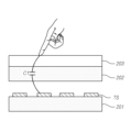
도 2는 본 실시예들에 따른 터치 디스플레이 장치(100)가 사용자의 터치를 센싱하는 방식을 나타낸 것이다.Figure 2 shows how the
도 2를 참조하면, 박막 트랜지스터 등이 배치된 제1기판(201)과 컬러 필터 등이 배치된 제2기판(202) 사이에 다수의 터치 센서(TS)가 분리되어 배치된다.Referring to FIG. 2, a plurality of touch sensors TS are separated and disposed between a
디스플레이 패널에 대한 사용자의 터치가 발생하면, 사용자의 손가락 등과 같은 포인터와 다수의 터치 센서(TS) 간의 캐패시턴스 변화가 발생하고, 이러한 캐패시턴스 변화를 센싱하여 사용자의 터치 유무와 터치 위치(터치 좌표)를 센싱할 수 있다.When a user's touch occurs on the display panel, a change in capacitance occurs between a pointer such as the user's finger and a plurality of touch sensors (TS), and this change in capacitance is sensed to determine the presence or absence of the user's touch and the touch location (touch coordinates). It can be sensed.
따라서, 본 실시예들에 따른 터치 디스플레이 장치(100)에 의하면, 디스플레이 장치의 기본 구조에서 공통 전극을 일정 영역별로 분리되도록 배치하여 터치 센서(TS)로 이용함으로써, 사용자의 터치 인식이 가능한 터치 디스플레이 장치(100)를 제공할 수 있다.Therefore, according to the
이러한 터치 디스플레이 장치(100)는, 전술한 터치 기능을 구현하기 위하여 데이터 라인과 평행한 별도의 터치 배선을 배치한다.This
이때, 터치 배선은 저항에 의한 딜레이를 저감하기 위하여 충분한 폭을 갖도록 설계되어야 한다.At this time, the touch wire must be designed to have a sufficient width to reduce delay due to resistance.
또한, 터치 배선으로 터치 구동 신호 인가 시 터치 배선과 평행하게 배치된 데이터 라인으로 인가되는 신호에 의해 터치 배선과 데이터 라인 사이에 미세한 캐패시턴스가 발생할 수 있다. 이러한 미세한 캐패시턴스는 터치 센서와 포인터 사이에 발생하는 캐패시턴스를 센싱하여 사용자의 터치를 센싱하는 데 영향을 줄 수 있다.Additionally, when a touch driving signal is applied to a touch wire, a small capacitance may occur between the touch wire and the data line due to the signal applied to the data line disposed parallel to the touch wire. This minute capacitance can affect sensing the user's touch by sensing the capacitance that occurs between the touch sensor and the pointer.
따라서, 터치 센싱에 영향을 주지 않도록 데이터 라인과 캐패시턴스가 발생되지 않는 구조로 설계되거나 터치 배선에 터치 구동 신호 인가 시 데이터 라인으로 유사한 신호(예: 동일 전위)를 인가하는 로드 프리 드라이빙(RFD: Road Free Driving)이 수행되어야 한다.Therefore, it is designed to have a structure that does not generate capacitance with the data line so as not to affect touch sensing, or load-free driving (RFD: Road) that applies a similar signal (e.g., the same potential) to the data line when a touch driving signal is applied to the touch wiring. Free Driving must be performed.
즉, 기존 디스플레이 장치의 구조에서 사용자의 터치를 센싱하기 위한 터치 배선의 설계는 터치 배선의 폭에 의한 개구율 감소, 다른 신호 배선과의 캐패시턴스 등을 고려하여 설계되어야 한다.That is, in the structure of an existing display device, the design of a touch wire for sensing a user's touch must be designed in consideration of the reduction in aperture ratio due to the width of the touch wire and capacitance with other signal wires.
이러한 터치 배선 설계는 대면적 디스플레이에서 더욱 어려움이 존재하며, 상호 정전 용량 방식에 비하여 많은 수의 터치 구동 회로가 요구되는 자기 정전 용량 방식에서는 대면적 터치 디스플레이 장치 구현 시, 터치 배선 설계, 터치 구동 회로와 터치 센서(TS) 수 증가에 따른 한계가 존재한다.Such touch wiring design is more difficult in large-area displays, and in the self-capacitance method, which requires a larger number of touch driving circuits than the mutual capacitance method, when implementing a large-area touch display device, touch wiring design, touch driving circuit There are limitations due to the increase in the number of touch sensors (TS).
본 실시예들은 터치 디스플레이 장치(100)의 터치 배선 구조를 개선함으로써, 대면적 디스플레이 장치에서도 사용자의 터치 인식이 가능한 터치 디스플레이 장치(100)를 제공한다.The present embodiments provide a
본 실시예들에 따른 터치 디스플레이 장치(100)는, 대면적 디스플레이 장치에서 사용자의 터치 인식이 가능하도록 하며, 이하에서는, 디스플레이 패널에서 부분적으로 터치 인식이 가능한 구조를 중심으로 설명하나 본 실시예들이 이에 한정되지는 아니한다.The
도 3은 제1실시예에 따른 터치 디스플레이 장치(100)의 개략적인 구성을 나타낸 것이다.FIG. 3 shows a schematic configuration of the
도 3을 참조하면, 제1실시예에 따른 터치 디스플레이 장치(100)에서 디스플레이 패널은 다수의 구동 화소가 배치된 표시 영역과 다수의 더미 화소(120)가 배치된 비표시 영역으로 구성될 수 있다.Referring to FIG. 3, in the
본 명세서에서 "구동 화소"는 표시 영역에서 게이트 라인과 데이터 라인에 의해 정의되는 영역에 배치되며 디스플레이 구동 구간에서 구동되는 화소를 의미한다. 그리고, "더미 화소"는 게이트 라인, 데이터 라인 등을 모두 포함하나, 구동 트랜지스터를 포함하지 않거나 구동 트랜지스터와 데이터 라인이 연결되지 않아 구동되지 않는 화소를 의미한다.In this specification, “driving pixel” refers to a pixel that is placed in an area defined by a gate line and a data line in the display area and is driven in the display driving section. And, a “dummy pixel” refers to a pixel that includes all gate lines, data lines, etc., but does not include a driving transistor or is not driven because the driving transistor and the data line are not connected.
디스플레이 패널의 표시 영역에는 사용자의 터치를 인식하기 위한 다수의 터치 센서(TS)가 배치되며, 패드부(110)에는 디스플레이 패널의 디스플레이 구동을 위한 드라이버 집적회로와 터치 구동을 위한 터치 구동 회로가 배치될 수 있다.A plurality of touch sensors (TS) are placed in the display area of the display panel to recognize the user's touch, and a driver integrated circuit for driving the display of the display panel and a touch driving circuit for touch driving are placed in the
패드부(110)에 배치된 터치 구동 회로와 표시 영역에 배치된 다수의 터치 센서(TS)는 비표시 영역에 배치된 다수의 더미 화소(120)를 통해 전기적으로 연결되며, 본 실시예들은 이를 통해 터치 배선을 단순화하며 사용자의 터치 인식이 가능한 디스플레이 장치를 제공하는 것을 특징으로 한다.The touch driving circuit disposed on the
또한, 터치 구동 회로와 다수의 터치 센서(TS)를 연결하는 다수의 더미 화소(120)는 하나의 예시에 해당하며, 비표시 영역에 배치된 전극 패턴이면 본 실시예들에 따른 터치 디스플레이 장치(100)에서 터치 구동 회로와 다수의 터치 센서(TS)를 전기적으로 연결하는 데 이용될 수 있다.In addition, the plurality of
다수의 터치 센서(TS)는, 디스플레이 패널에서 다수의 구동 화소가 배치된 표시 영역의 일부 영역에 서로 이격되어 일렬로 배치될 수 있다.A plurality of touch sensors TS may be arranged in a row and spaced apart from each other in a portion of the display area where a plurality of driving pixels are arranged on the display panel.
다수의 터치 센서(TS)는, 도 3에 도시된 바와 같이, 횡방향으로 배치될 수도 있으나 종방향으로 배치될 수도 있다.As shown in FIG. 3, the plurality of touch sensors TS may be arranged horizontally or vertically.
다수의 터치 센서(TS)는, 서로 이격되어 배치됨으로써 사용자의 터치 유무와 터치 위치(터치 좌표)를 센싱할 수 있도록 하며, 사용자의 터치의 횡방향 움직임에 따른 드래그 터치를 센싱할 수 있도록 한다.A plurality of touch sensors (TS) are arranged to be spaced apart from each other to sense the presence or absence of a user's touch and the touch location (touch coordinates), and to sense a drag touch according to the lateral movement of the user's touch.
디스플레이 패널의 비표시 영역에는 다수의 더미 화소(120)가 배치되어 있다.A plurality of
다수의 더미 화소(120)는, 인접한 더미 화소(120)끼리 전기적으로 연결되나, 더미 화소(120)와 연결되는 터치 센서(TS)에 폭에 해당하는 더미 화소(120) 단위로 분리되어 배치될 수 있다.The plurality of
즉, 터치 센서(TS)의 폭에 해당하는 단위로 분리되어 더미 화소(120)가 배치될 수 있다.That is, the
본 실시예들에 따른 터치 디스플레이 장치(100)는, 디스플레이 패널의 비표시 영역에 배치된 다수의 더미 화소(120)를 통해 디스플레이 패널에 배치된 다수의 터치 센서(TS)와 패드부(110)에 배치된 터치 구동 회로를 연결함으로써, 별도의 터치 배선 없이 사용자의 터치를 센싱할 수 있도록 한다.The
즉, 별도의 터치 배선을 제작하는 공정 없이, 더미 화소(120)에 포함된 화소 전극 등을 제작하는 과정에서 다수의 터치 센서(TS)와 터치 구동 회로를 연결하는 터치 배선이 형성되도록 함으로써, 제작 공정 과정을 감소시키면서 터치 배선 설계를 용이하게 한다.That is, the touch wires connecting a plurality of touch sensors TS and the touch driving circuit are formed in the process of manufacturing the pixel electrodes included in the
도 4는 제1실시예에 따른 터치 디스플레이 장치(100)의 구체적인 연결 관계 구조를 나타낸 것이다.FIG. 4 shows a specific connection relationship structure of the
도 4를 참조하면, 패드부(110)에 배치된 터치 구동 회로(112)는 제1연결부(121)를 통해 디스플레이 패널의 비표시 영역에 배치된 다수의 더미 화소(120)와 전기적으로 연결된다.Referring to FIG. 4, the
그리고, 다수의 더미 화소(120)는, 제2연결부(122)를 통해 디스플레이 패널의 표시 영역에 배치된 다수의 터치 센서(TS)와 전기적으로 연결된다.In addition, the plurality of
다수의 더미 화소(120)는 동일한 터치 센서(TS)와 전기적으로 연결된 더미 화소(120)끼리 서로 전기적으로 연결되며, 다른 터치 센서(TS)와 전기적으로 연결된 더미 화소(120)와는 이격되어 배치된다.The plurality of
이때, 제1연결부(121)와 제2연결부(122)는, 다수의 더미 화소(120)에 포함된 화소 전극을 구성하는 물질과 동일한 물질(예: 화소 메탈)로 구성될 수 있다.At this time, the
따라서, 다수의 더미 화소(120)에 포함된 화소 전극을 제작하는 과정에서 제1연결부(121)와 제2연결부(122)를 제작하여 터치 배선을 형성하도록 함으로써, 터치 배선의 제작을 위한 별도의 공정이 필요하지 않도록 한다.Therefore, in the process of manufacturing the pixel electrodes included in the plurality of
즉, 터치 배선 구현을 위한 마스크(Mask) 수를 감소시키면서 사용자의 터치 센싱이 가능할 수 있도록 한다.In other words, it enables user touch sensing while reducing the number of masks for implementing touch wiring.
제2연결부(122)는, 다수의 터치 센서(TS)에 대응하는 영역에 배치된 구동 화소의 화소 메탈을 통해 다수의 터치 센서(TS)와 전기적으로 연결될 수 있다.The
즉, 터치 구동 구간 동안 터치 구동 회로(112)로부터 출력된 터치 구동 신호는 제1연결부(121), 더미 화소(120), 제2연결부(122), 그리고 구동 화소에 포함된 화소 메탈을 통해 터치 센서(TS)로 전달될 수 있다.That is, the touch driving signal output from the
따라서, 본 실시예들에 의하면, 디스플레이 패널의 비표시 영역에 배치되는 다수의 더미 화소(120)를 이용하여 터치 배선을 구현함으로써, 터치 배선 설계를 단순화하고, 터치 배선 설계를 위한 공정의 수를 감소시키며 사용자의 터치 인식이 가능한 터치 디스플레이 장치(100)를 제공할 수 있도록 한다.Therefore, according to the present embodiments, the touch wiring design is simplified and the number of processes for touch wiring design is reduced by implementing the touch wiring using a plurality of
도 5는 제1실시예에 따른 터치 디스플레이 장치(100)에서 다수의 터치 센서(TS)와 터치 구동 회로(112)가 연결되는 연결 부분을 나타낸 평면도이다.FIG. 5 is a plan view showing a connection portion where a plurality of touch sensors TS and the
도 5를 참조하면, 디스플레이 패널의 표시 영역에서 비표시 영역에 인접한 영역에 배치되는 다수의 터치 센서(TS)는 일정한 크기로 이루어지며, 터치 센서(TS)마다 이격되어 배치되어 있다.Referring to FIG. 5 , a plurality of touch sensors TS disposed in an area adjacent to a non-display area in the display area of the display panel are made of a certain size and are arranged to be spaced apart from each other.
또한, 터치 센서(TS)의 경계에 위치하는 구동 화소끼리 서로 이격되어 배치된다.Additionally, driving pixels located at the border of the touch sensor TS are arranged to be spaced apart from each other.
각각의 터치 센서(TS)는, 다수의 더미 화소(120)를 통해 패드부(110)에 배치된 터치 구동 회로(112)와 전기적으로 연결된다.Each touch sensor TS is electrically connected to the
다수의 더미 화소(120)는 동일한 터치 센서(TS)와 연결된 더미 화소(120)끼리 서로 전기적으로 연결되어 있으며, 다른 터치 센서(TS)와 연결된 더미 화소(120)와는 이격되어 배치된다.The plurality of
따라서, 터치 구동 구간 동안 터치 구동 회로(112)로부터 출력되는 터치 구동 신호가 서로 전기적으로 연결된 더미 화소(120)를 통해 각각의 터치 센서(TS)로 전달된다.Accordingly, during the touch driving period, the touch driving signal output from the
디스플레이 패널의 비표시 영역에 배치된 다수의 더미 화소(120)를 터치 센서(TS) 단위로 분리하고, 터치 센서(TS)와 터치 구동 회로(112)를 전기적으로 연결함으로써, 더미 화소(120)를 이용한 터치 배선을 구현할 수 있도록 한다.By separating the plurality of
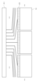
도 6a와 도 6b는 제1실시예에 따른 터치 디스플레이 장치(100)에서 화소 전극을 터치 배선화한 경우 구동 화소의 평면과 단면을 나타낸 것으로서, 도 6b는 도 6a에서 A-A'의 단면을 나타낸 것이다.FIGS. 6A and 6B show the plane and cross section of the driving pixel when the pixel electrode is touch wired in the
도 6b를 참조하면, 기판(601) 상에 게이트 메탈(602)이 배치되며, 그 위에 게이트 절연층(603)이 배치된다. 게이트 절연층(603) 상에 데이터 라인(604), 그리고 컬러 필터 등이 배치되고, 그 위에 유기막 또는 무기막(605)이 배치되며, 유기막 또는 무기막(605)의 상면에 공통 전극(606)과 화소 전극(607)이 배치된다.Referring to FIG. 6B, a
게이트 메탈(602)과 데이터 라인(604)은 터치 디스플레이 장치(100)가 디스플레이 구동을 하는 동안에 신호 전달 배선으로 사용된다.The
게이트 메탈(602)은 게이트 메탈(602)의 상층에 위치하는 게이트 절연층(603)과 유기막 또는 무기막(605)에 형성된 컨택홀을 통해 유기막 또는 무기막(605)의 상면에 위치하는 공통 전극(606)과 전기적으로 연결된다.The
즉, 게이트 메탈(602)은 디스플레이 구동 구간에서 공통 전극(606)으로 공통 전압을 전달하는 신호 배선으로 사용된다.That is, the
데이터 라인(604)은 구동 트랜지스터를 구성하는 액티브층이나 소스/드레인 전극을 구성하는 물질로 이루어질 수 있다.The
데이터 라인(604)은 데이터 라인(604)의 상층에 위치하는 유기막 또는 무기막(605)에 형성된 컨택홀을 통해 유기막 또는 무기막(605)의 상면에 위치하는 화소 전극(607)과 전기적으로 연결된다.The
따라서, 디스플레이 구동 구간에서, 공통 전압은 게이트 메탈(602)을 통해 공통 전극(606)으로 인가되고, 데이터 전압은 데이터 라인(604)을 통해 화소 전극(607)으로 인가된다.Accordingly, in the display driving section, the common voltage is applied to the
한편, 터치 구동 구간에서는, 터치 배선을 통해 터치 구동 신호가 터치 센서(TS)에 인가되고, 포인터와 터치 센서(TS) 사이의 캐패시턴스 변화를 센싱하여 사용자의 터치를 센싱할 수 있도록 한다.Meanwhile, in the touch driving section, a touch driving signal is applied to the touch sensor (TS) through the touch wiring, and the change in capacitance between the pointer and the touch sensor (TS) is sensed to sense the user's touch.
여기서, 터치 센서(TS)는, 유기막 또는 무기막(605)의 상면에 위치하는 공통 전극(606)일 수 있다.Here, the touch sensor TS may be a
즉, 공통 전극(606)은, 디스플레이 구동 구간에서는 공통 전압이 인가되는 전극으로서 기능을 하고, 터치 구동 구간에서는 터치 구동 신호가 인가되는 터치 센서(TS)로서의 기능을 한다.That is, the
제1실시예에 따른 터치 디스플레이 장치(100)에서는, 유기막 또는 무기막(605)의 상면에 배치되는 화소 메탈을 터치 배선화함으로써 터치 배선을 위한 별도의 신호 라인이나 층이 필요하지 않도록 한다.In the
즉, 구동 화소에 포함된 화소 메탈이 더미 화소(120)에 연결된 제2연결부(122)와 전기적으로 연결되어, 터치 구동 회로(112)로부터 출력된 터치 구동 신호가 제1연결부(121), 더미 화소(120), 제2연결부(122), 그리고 구동 화소에 포함된 화소 메탈을 통해 터치 센서(TS)인 공통 전극(606)으로 전달되게 된다.That is, the pixel metal included in the driving pixel is electrically connected to the
따라서, 디스플레이 패널에서 터치 센서(TS)가 배치된 영역에 위치하는 구동 화소에는, 터치 센서(TS)와 터치 구동 회로를 연결하기 위한 터치 배선이 별도로 배치되지 않게 된다. 이를 통해 터치 배선을 위해 필요한 공정을 감소시키고 단순화된 화소 구조를 제공하면서 사용자의 터치 인식이 가능하도록 하는 이점을 제공한다.Accordingly, in the driving pixel located in the area where the touch sensor TS is placed in the display panel, a separate touch wire for connecting the touch sensor TS and the touch driving circuit is not disposed. This provides the advantage of reducing the process required for touch wiring, providing a simplified pixel structure, and enabling user touch recognition.
한편, 제2실시예에 따른 터치 디스플레이 장치(100)는 디스플레이 패널의 비표시 영역에 배치된 다수의 더미 화소(120)를 이용하여 터치 구동 회로(112)와 터치 센서(TS)를 연결함에 있어서, 더미 화소(120)에 포함된 소스 라인을 통해 터치 배선을 구현함으로써 터치 인식의 성능을 더욱 향상시킬 수 있다.Meanwhile, the
예를 들어, 일반적인 화소 구조에서는 하나의 화소마다 한 개의 게이트 라인과 한 개의 데이터 라인(604, 소스 라인)이 교차되어 배치되나, 하나의 데이터 라인(604)을 양쪽 화소에서 공통으로 이용하는 구조에서는 두 개의 화소마다 하나의 데이터 라인(604)이 배치되므로 데이터 라인(604)이 배치되지 않는 영역이 존재한다.For example, in a general pixel structure, one gate line and one data line (604, source line) are arranged to intersect each pixel, but in a structure in which one data line (604) is commonly used by both pixels, there are two Since one
즉, 두 개의 화소마다 하나의 데이터 라인(604)이 배치되는 구조에서, 데이터 라인(604)이 배치되지 않는 영역에 소스 라인을 배치하고 배치된 소스 라인을 터치 배선으로 이용함으로써, 별로의 터치 배선을 구성하지 않고 사용자의 터치 인식이 가능하도록 할 수 있다.That is, in a structure in which one
도 7은 제2실시예에 따른 터치 디스플레이 장치(100)의 개략적인 구성을 나타낸 것으로서, 두 개의 화소마다 하나의 데이터 라인(604)이 배치되는 구조에서 터치 배선을 구현한 예를 나타낸 것이다.FIG. 7 shows a schematic configuration of the
도 7을 참조하면, 제2실시예에 따른 터치 디스플레이 장치(100)에서 디스플레이 패널의 표시 영역에 다수의 터치 센서(TS)가 서로 이격되어 일렬로 배치된다.Referring to FIG. 7, in the
다수의 터치 센서(TS)는, 디스플레이 패널에 배치된 다수의 더미 화소(120)를 통해 패드부(110)에 배치된 터치 구동 회로(112)와 연결된다.The multiple touch sensors TS are connected to the
이때, 다수의 터치 센서(TS)와 터치 구동 회로(112)는 다수의 더미 화소(120)에 포함된 소스 라인을 통해 전기적으로 연결되는 것을 특징으로 한다.At this time, the plurality of touch sensors TS and the
즉, 더미 화소(120)에 포함된 소스 라인을 제작하는 과정에서 더미 화소(120)와 터치 구동 회로(112)를 연결하는 배선과, 더미 화소(120)와 터치 센서(TS)를 연결하는 배선을 함께 구성하여 터치 구동 회로(112)와 다수의 터치 센서(TS)가 더미 화소(120)를 통해 연결될 수 있도록 한다.That is, in the process of manufacturing the source line included in the
여기서, 더미 화소(120)와 터치 센서(TS)를 연결하는 배선은, 표시 영역에 배치된 구동 화소에서 데이터 라인(604)이 배치되지 않은 영역에 위치하는 소스 라인을 통해 다수의 터치 센서(TS)와 연결된다.Here, the wiring connecting the
또는, 구동 화소에 포함된 화소 메탈을 통해 다수의 터치 센서(TS)와 연결될 수도 있다.Alternatively, it may be connected to a plurality of touch sensors (TS) through pixel metal included in the driving pixel.
구동 화소에 포함된 화소 메탈이 아닌 소스 라인을 통해 다수의 터치 센서(TS)와 연결되는 경우에는, 화소 메탈에 비해 소스 라인의 두께가 두꺼우므로 화소 메탈에 비해 저항이 1/100 수준에 해당한다. 따라서, 화소 메탈을 통해 터치 구동 신호를 전달하는 경우에 비해 소스 라인의 길이를 길게 설계할 수 있으므로, 터치 센싱이 가능한 영역을 확장할 수 있는 이점이 존재한다.When connected to multiple touch sensors (TS) through source lines other than the pixel metal included in the driving pixel, the thickness of the source line is thicker than the pixel metal, so the resistance is 1/100th of that of the pixel metal. . Therefore, compared to the case where the touch driving signal is transmitted through the pixel metal, the length of the source line can be designed to be longer, which has the advantage of expanding the area where touch sensing is possible.
또한, 데이터 라인(604)이 배치되지 않는 영역에 소스 라인을 배치하고 배치된 소스 라인을 터치 배선으로 이용함으로써, 터치 배선과 데이터 라인(604)이 평행하게 배치되는 경우 발생하는 캐패시턴스의 영향을 받지 않도록 터치 배선을 설계할 수 있다.In addition, by placing the source line in an area where the
따라서, 데이터 라인(604)이 배치되지 않는 영역에 배치되며 화소 메탈의 저항의 1/100 수준인 소스 라인을 터치 배선으로 이용하는 경우, RC 로드를 저감시켜 대면적 디스플레이 패널에서도 넓은 영역에서 사용자의 터치 센싱이 가능한 터치 배선 구조를 제공할 수 있다.Therefore, when the source line, which is placed in an area where the
도 8은 제2실시예에 따른 터치 디스플레이 장치(100)에서 더미 화소(120)를 통해 터치 구동 회로(112)와 다수의 터치 센서(TS)가 연결되는 구체적인 구조를 나타낸 것이다.FIG. 8 shows a specific structure in which the
도 8을 참조하면, 패드부(110)에 배치된 터치 구동 회로(112)와 표시 영역에 배치되는 다수의 터치 센서(TS)는, 비표시 영역에 배치된 다수의 더미 화소(120)를 통해 전기적으로 연결된다.Referring to FIG. 8, the
터치 구동 회로(112)와 더미 화소(120)를 연결하는 제1연결부(121)와 더미 화소(120)와 다수의 터치 센서(TS)를 연결하는 제2연결부(122)를 통해 터치 구동 회로(112)와 다수의 터치 센서(TS)가 전기적으로 연결될 수 있도록 한다.A touch driving circuit ( 112) and a plurality of touch sensors (TS) can be electrically connected.
이때, 제1연결부(121)와 제2연결부(122)는, 다수의 더미 화소(120)에 포함된 소스 라인을 구성하는 물질과 동일한 물질(예: 소스 메탈)로 이루어질 수 있다.At this time, the
즉, 다수의 더미 화소(120)에 포함된 소스 라인을 제작하는 과정에서 제1연결부(121)와 제2연결부(122)를 함께 제작할 수 있도록 하여, 터치 배선의 제작을 위한 별도의 공정이 필요하지 않도록 하는 이점을 제공한다.That is, the
제2연결부(122)는, 제1실시예에서와 같이 표시 영역에 배치된 구동 화소에 포함된 화소 메탈을 통해 다수의 터치 센서(TS), 즉, 공통 전극(606)과 전기적으로 연결될 수 있다.As in the first embodiment, the
제2연결부(122)가 구동 화소에 포함된 화소 메탈과 연결되는 경우, 제2연결부(122)가 구동 화소에서 데이터 라인(604)이 배치되는 층의 상층에 배치된 절연층에 형성되는 컨택홀을 통해 화소 메탈과 전기적으로 연결될 수 있다.When the
또는, 제2연결부(122)는, 표시 영역에 배치된 구동 화소에 포함된 소스 라인을 통해 다수의 터치 센서(TS)와 전기적으로 연결될 수 있다.Alternatively, the
여기서, 제2연결부(122)가 연결되는 소스 라인은, 구동 화소에서 데이터 라인(604)이 배치되지 않은 영역에 배치되는 소스 라인을 의미하는 것으로서, 데이터 라인(604)이 배치되지 않은 영역에 소스 라인을 배치하고 배치된 소스 라인을 터치 배선으로 이용하는 것이다.Here, the source line to which the
따라서, 제2연결부(122)가 구동 화소에 포함된 화소 메탈을 통해 터치 센서(TS)와 연결되는 경우에 비하여, 소스 라인을 통해 터치 센서(TS)와 연결됨으로써 터치 센서(TS)의 세로 길이를 길게 구성할 수 있는 이점을 제공한다. 이를 통해, 디스플레이 패널의 하단부에 구현되는 터치 인식 가능 영역을 확장시킬 수 있도록 한다.Therefore, compared to the case where the
또한, 터치 센싱 가능 영역이 디스플레이 패널의 세로 방향으로 확장됨에 따라, 디스플레이 패널의 하단부뿐만 아니라 디스플레이 패널의 중앙 부분에서 사용자의 터치를 센싱할 수 있도록 한다.Additionally, as the touch sensing area expands in the vertical direction of the display panel, the user's touch can be sensed not only at the bottom of the display panel but also at the center of the display panel.
즉, 소스 라인을 통해 터치 배선을 구현하는 경우, 디스플레이 패널의 하단부에서 터치 센싱이 가능하도록 하거나, 또는 중앙 부분에서 터치 센싱이 가능하도록 하거나, 또는 하단부와 중앙 부분에서 모두 사용자의 터치를 센싱할 수 있도록 할 수 있다.In other words, when implementing a touch wiring through a source line, touch sensing is possible at the bottom of the display panel, touch sensing is possible at the center, or the user's touch can be sensed at both the bottom and the center. It can be done.
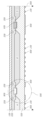
도 9a와 도 9b는 제2실시예에 따른 터치 디스플레이 장치(100)에서, 구동 화소에 소스 라인을 통해 터치 배선을 형성한 경우의 평면과 단면을 나타낸 것으로서, 도 9b는 도 9a의 A-A'의 단면을 나타낸 것이다.FIGS. 9A and 9B show a plane and cross section of the
도 9b를 참조하면, 기판(301) 상에 게이트 메탈(602)이 배치되며, 그 위에 게이트 절연층(603)이 배치된다. 게이트 절연층(603) 상에 데이터 라인(604), 그리고 컬러 필터 등이 배치되고, 그 위에 유기막 또는 무기막(605)이 배치되며, 유기막 또는 무기막(605)의 상면에 공통 전극(606)과 화소 전극(607)이 배치된다.Referring to FIG. 9B, a
디스플레이 구동 구간에서, 게이트 메탈(602)을 통해 공통 전극(606)으로 공통 전압이 인가되고, 스캔 신호가 인가되면 데이터 라인(604)을 통해 데이터 전압이 화소 전극(607)으로 인가되어 디스플레이 구동을 수행한다.In the display driving section, a common voltage is applied to the
터치 구동 구간에서는, 터치 배선을 통해 터치 구동 신호가 터치 센서(TS)에 인가되고, 포인터와 터치 센서(TS) 사이의 캐패시턴스 변화를 센싱하여 사용자의 터치를 센싱할 수 있도록 한다.In the touch driving section, a touch driving signal is applied to the touch sensor (TS) through the touch wiring, and the change in capacitance between the pointer and the touch sensor (TS) is sensed to sense the user's touch.
제2실시예에 따른 터치 디스플레이 장치(100)에서는, 유기막 또는 무기막(605)의 상면에 배치되는 화소 메탈을 터치 배선으로 이용할 수도 있으나, 데이터 라인(604)이 배치되지 않는 영역인 900 영역에 소스 라인(608)을 배치하고 배치된 소스 라인(608)을 터치 배선으로 이용할 수도 있다.In the
즉, 각각의 구동 화소마다 데이터 라인(604)이 배치되는 구조에서는 구동 화소에 포함된 화소 메탈을 터치 배선으로 이용하고, 두 개의 구동 화소마다 하나의 데이터 라인(604)이 배치되는 구조에서는 화소 메탈을 터치 배선으로 이용하거나 데이터 라인(604)이 배치되지 않는 영역에 소스 라인(608)을 배치하고 이를 터치 배선으로 이용한다.That is, in a structure in which a
따라서, 구동 화소에 포함된 화소 메탈 또는 소스 라인(608)을 터치 배선으로 이용함으로써, 터치 배선을 위한 별도의 제작 공정이 필요하지 않도록 하는 이점을 제공한다.Accordingly, using the pixel metal or
또한, 구동 화소에 배치된 소스 라인(608)으로 터치 배선을 구현할 경우, 화소 메탈에 비해 소스 라인(608)의 두께가 두꺼워 저항이 1/100 수준이므로 배선의 저항에 의한 딜레이를 감소시켜 화소 메탈으로 터치 배선을 구현하는 경우보다 터치 인식 가능 영역을 확장시킬 수 있는 이점을 제공한다.In addition, when implementing a touch wiring with the
또한, 터치 배선이 데이터 라인(604)과 평행하게 배치되지 않는 구조를 통해 데이터 라인(604)과의 캐패시턴스에 의한 영향을 감소시켜, 터치 배선의 RC 로드를 저감시키면서 사용자의 터치를 센싱할 수 있는 터치 배선 구조를 제공한다.In addition, the effect of capacitance with the
도 10 내지 도 13은 도 9의 900 영역을 확대하여 나타낸 것으로서, 두 개의 구동 화소마다 하나의 데이터 라인(604)이 배치되는 구조에서 구동 화소에 포함된 화소 메탈 또는 소스 라인(608)을 통해 터치 배선을 구현한 예를 나타낸 것이다.FIGS. 10 to 13 are enlarged illustrations of
도 10과 도 11은 구동 화소에 포함된 화소 전극(607)을 터치 배선으로 구현한 경우의 예를 나타낸 것으로서, 표시 영역에 배치된 구동 화소에서 유기막 또는 무기막(605)의 상면에 위치하는 화소 메탈을 터치 배선으로 구현한 경우를 나타낸 것이다.Figures 10 and 11 show an example of a case where the
도 10을 참조하면, 유기막 또는 무기막(605)의 상면에 위치하는 화소 메탈을 터치 배선으로 구현할 수 있으며, 도 10은 유기막 또는 무기막(605)의 상면에 배치되는 화소 메탈을 단일 배선으로 구현한 경우를 나타낸 것이다.Referring to FIG. 10, the pixel metal located on the top surface of the organic or
도 11은 유기막 또는 무기막(605)의 상면에 위치하는 화소 메탈을 터치 배선으로 구현하되, 유기막 또는 무기막(605)의 상면에 배치되는 화소 메탈을 복수 배선으로 구현한 경우를 나타낸 것이다.FIG. 11 shows a case where the pixel metal located on the top surface of the organic film or
따라서, 본 실시예들에 의하면, 화소 메탈을 터치 배선으로 구현하는 경우, 터치 배선은 단일 배선이나 복수 배선으로 구현될 수 있다.Therefore, according to the present embodiments, when the pixel metal is implemented as a touch wire, the touch wire may be implemented as a single wire or multiple wires.
도 12와 도 13은 구동 화소에 포함된 소스 라인(608)을 터치 배선으로 구현한 경우의 예를 나타낸 것으로서, 구동 화소에서 데이터 라인(604)이 배치되지 않는 영역에 소스 라인(608)을 배치하고 배치된 소스 라인(608)을 터치 배선으로 이용하는 경우를 나타낸 것이다.12 and 13 show an example of a case where the
도 12를 참조하면, 데이터 라인(604)이 배치되는 층과 동일한 층에서 데이터 라인(604)이 배치되지 않는 영역에 소스 라인(608)을 배치하고 배치된 소스 라인(608)을 터치 배선으로 이용하며, 도 12는 배치되는 소스 라인(608)을 단일 배선으로 구현한 경우를 나타낸 것이다.Referring to FIG. 12, the
도 13은 데이터 라인(604)이 배치되지 않는 영역에 소스 라인(608)을 배치하여 터치 배선으로 구현하되, 소스 라인(608)을 복수 배선으로 구현한 경우를 나타낸 것이다.FIG. 13 shows a case where the
따라서, 본 실시예들에 의하면, 데이터 라인(604)이 배치되지 않는 영역에 소스 라인(608)을 배치하여 터치 배선으로 이용하는 경우, 터치 배선은 단일 배선이나 복수 배선으로 구현될 수 있다.Therefore, according to the present embodiments, when the
한편, 제3실시예에 따른 터치 디스플레이 장치(100)에서는, 터치 구동 회로(112)와 다수의 터치 센서(TS)가 비표시 영역에 배치된 더미 화소(120)를 통해 연결되는 경우, 화소 전극(607) 또는 소스 라인(608)이 배치되는 층과 다른 층에 위치하는 신호 라인을 통해 연결될 수도 있다.Meanwhile, in the
즉, 더미 화소(120)를 통해 터치 구동 회로(112)와 다수의 터치 센서(TS)가 연결되는 경우에도, 별로의 터치 배선을 통해 사용자의 터치 인식이 가능하도록 할 수도 있다.That is, even when the
예를 들어, 터치 구동 회로(112), 더미 화소(120) 및 터치 센서(TS)를 연결하는 제1연결부(121)와 제2연결부(122)를 별도의 신호 라인으로 구현할 수 있다.For example, the
이하에서는, 제1연결부(121)와 제2연결부(122)가 화소 전극(607) 또는 소스 라인(608)이 배치되는 층과 다른 층에 위치하는 신호 라인을 통해 구현되는 경우, 구동 화소에서 터치 배선이 구현된 예를 설명한다.Hereinafter, in the case where the
도 14는 제3실시예에 따른 터치 디스플레이 장치(100)에서 구동 화소의 단면을 나타낸 것으로서, 두 개의 화소마다 데이터 라인(604)이 배치되는 구조에서 구동 화소에 포함된 화소 전극(607)이나 소스 라인(608)이 배치되는 층과 다른 층에 위치하는 신호 라인이 터치 배선으로 구현된 예를 나타낸 것이다.FIG. 14 shows a cross section of a driving pixel in the
도 14를 참조하면, 기판(601) 상에 게이트 메탈(602)이 배치되며, 그 위에 게이트 절연층(603)이 배치된다. 게이트 절연층(603) 상에 데이터 라인(604) 그리고 컬러 필터 등이 배치되고, 그 위에 유기막 또는 무기막(605)이 배치된다.Referring to FIG. 14, a
그리고, 유기막 또는 무기막(605)의 상면에 신호 라인(609)을 배치하고 그 상층에 공통 전극(606)과 화소 전극(607)이 배치된다.Then, a
신호 라인(609)은 데이터 라인(604)이 배치되지 않는 영역에서 데이터 라인(604)이 배치되는 층과 다른 층에 배치될 수 있다.The
따라서, 비표시 영역에 포함된 구동 화소(120)를 이용하여 터치 구동 회로(112)와 터치 센서(TS)를 연결하는 경우에도, 화소 전극(607)이나 소스 라인(608)이 배치되지 않는 층에 위치하는 신호 라인(609)을 배치하여 터치 인식이 가능하도록 할 수도 있다.Therefore, even when the
화소 전극(607)이나 소스 라인(608)이 배치되는 층과 다른 층에 위치하는 신호 라인(609)을 이용하여 터치 배선을 구현하는 경우, 신호 라인(609)의 두께를 고려할 때 화소 메탈에 비하여 저항이 1/100 수준이므로 터치 가능 영역을 확장시킬 수 있는 이점을 제공한다.When implementing a touch wiring using a
또한, 별도의 신호 라인(609)을 이용하여 터치 배선을 구현하는 경우에, 데이터 라인(604)이 배치되지 않는 영역마다 신호 라인(609)을 배치하여 터치 배선을 구현할 수도 있으나, 도 14에 도시된 바와 같이 소스 라인(608)과 신호 라인(609)을 모두 이용하여 터치 배선을 구현할 수도 있다.Additionally, when implementing the touch wiring using a
이때, 터치 배선으로 구현되는 소스 라인(608)과 신호 라인(609)은 데이터 라인(604)이 배치되지 않는 영역마다 교번하여 배치될 수도 있으며, 서로 동일한 영역에 중복되어 배치될 수도 있다.At this time, the
즉, 본 실시예들에 의하면, 비표시 영역에 배치된 더미 화소(120)를 이용하여 터치 구동 회로(112)와 다수의 터치 센서(TS)을 연결하는 터치 배선을 구현하는 경우, 화소 메탈, 소스 라인(608), 또는 별도의 신호 라인(609) 등 다양한 방식으로 터치 배선의 구현이 가능하도록 함으로써 제품 특성에 맞게 터치 배선을 설계할 수 있도록 한다.That is, according to the present embodiments, when implementing a touch wiring connecting the
도 15와 도 16은 제3실시예에 따른 터치 디스플레이 장치(100)의 단면에서 1400 영역의 구현 예를 나타낸 것이다.Figures 15 and 16 show an implementation example of
도 15는 터치 배선이 화소 전극(607)이나 소스 라인(608)이 배치되지 않는 층에 위치하는 신호 라인(609)으로만 구현되거나, 소스 라인(608)과 신호 라인(609)을 통해 구현되는 경우 중 교번하여 배치되는 경우를 나타낸 것이다.15 shows that the touch wire is implemented only with the
도 15를 참조하면, 구동 화소에서 데이터 라인(604)이 배치되지 않는 영역의 상층에 신호 라인(609)이 배치되어 터치 배선으로 이용된다.Referring to FIG. 15, a
도 16은 터치 배선이 소스 라인(608)과 신호 라인(609)을 이용하여 구현되는 경우를 나타낸 것으로서, 소스 라인(608)과 신호 라인(609)이 데이터 라인(604)이 배치되지 않는 영역에 중복되어 배치되는 경우를 나타낸 것이다.Figure 16 shows a case where the touch wire is implemented using the
도 16을 참조하면, 데이터 라인(604)이 배치되지 않는 영역에 소스 라인(608)과 신호 라인(609)이 모두 배치되어 터치 배선이 구현될 수 있으며, 이때 신호 라인(609)은 소스 라인(608)과 중첩되는 영역으로부터 일정 거리만큼 이격되어 배치될 수도 있다.Referring to FIG. 16, a touch wiring can be implemented by placing both the
따라서, 비표시 영역에 배치된 더미 화소(120)를 통해 터치 구동 회로(112)와 터치 센서(TS)가 연결되는 경우에도, 화소 전극(607)이나 소스 라인(608)이 배치되는 층과 다른 층에 위치하는 신호 라인(609)을 통해 터치 배선이 구현될 수 있다.Therefore, even when the
또한, 데이터 라인(604)이 배치되지 않는 영역에 신호 라인(609)으로 터치 배선을 구현하는 경우에도 소스 라인(608)과 함께 터치 배선을 구현할 수 있다.Additionally, even when the touch wiring is implemented using the
이때, 신호 라인(609)은 소스 라인(608)과 교번 배치, 중복 배치될 수 있으며, 중복 배치되는 경우 중첩되는 영역으로부터 일정 거리만큼 이격되어 배치될 수도 있어 다양한 구조로 터치 배선을 구현할 수 있다.At this time, the
도 17a와 도 17b는 제4실시예에 따른 터치 디스플레이 장치(100)에서 구동 화소의 평면과 단면을 나타낸 것이다.FIGS. 17A and 17B show the plane and cross section of the driving pixel in the
도 17a를 참조하면, 각각의 화소마다 데이터 라인(604)이 배치되는 구조에서 화소 전극(607)이나 소스 라인(608)이 배치되지 않는 층과 다른 층에 위치하는 신호 라인(609)을 통해 터치 배선을 구현한 경우를 나타낸 것으로서, 도 17b는 도 17a에서 A-A'의 단면을 나타낸 것이다.Referring to FIG. 17A, in a structure in which the
도 17b를 참조하면, 기판(601) 상에 게이트 메탈(602)이 배치되며, 그 위에 게이트 절연층(603)이 배치된다. 게이트 절연층(603) 상에 데이터 라인(604), 그리고 컬러 필터 등이 배치되고, 그 위에 유기막 또는 무기막(605)이 배치된다.Referring to FIG. 17B, a
유기막 또는 무기막(605)의 상면에 신호 라인(609)이 배치되며, 신호 라인(609)의 상층에 공통 전극(606)과 화소 전극(607)이 배치된다.A
따라서, 다수의 터치 센서(TS)와 전기적으로 연결되는 제2연결부(122)는, 화소 전극(607)이나 소스 라인(608)과 다른 층에 배치되는 신호 라인(609)을 통해 터치 센서(TS)와 연결된다.Accordingly, the
신호 라인(609)은 화소 메탈보다 두께가 두꺼워 화소 메탈에 비하여 저항이 1/100 수준이므로, 화소 메탈을 통해 터치 센서(TS)에 연결되는 경우에 비하여 터치 가능 영역을 넓게 구현할 수 있는 이점을 제공한다.The
또한, 신호 라인(609)과 데이터 라인(604) 사이의 캐패시턴스에 따라 신호 라인(609)과 데이터 라인(604)과 중첩된 영역에 배치하거나, 중첩된 영역으로부터 이격되도록 배치하여 터치 센싱이 가능한 RC 로드를 만족시키며 터치 배선을 구현할 수 있다.In addition, depending on the capacitance between the
도 18과 도 19는 도 17b의 1700 영역을 확대하여 나타낸 것으로서, 각각의 화소마다 데이터 라인(604)이 배치되는 구조에서 별도의 신호 라인(609)으로 구현된 터치 배선의 예를 나타낸 것이다.FIGS. 18 and 19 are enlarged views of
도 18을 참조하면, 데이터 라인(604)이 배치되는 영역의 상층에 신호 라인(609)이 배치되며, 신호 라인(609)이 데이터 라인(604)과 중첩되는 영역에 배치되는 경우를 나타낸 것이다.Referring to FIG. 18 , the
도 19를 참조하면, 데이터 라인(604)이 배치되는 영역의 상층에 신호 라인(609)이 배치되되, 신호 라인(609)이 데이터 라인(604)과 중첩되는 영역으로부터 일정 거리만큼 이격되어 배치된 경우를 나타낸 것이다.Referring to FIG. 19, the
따라서, 데이터 라인(604)의 상층에 신호 라인(609)을 배치하고 터치 배선으로 이용하는 경우, 데이터 라인(604)과 신호 라인(609)의 캐패시턴스에 따라 중첩되는 구조 또는 중첩되는 영역으로부터 이격되는 구조 등 다양하게 설계가 가능하다.Therefore, when the
전술한 실시예들에서는, 디스플레이 패널의 하단부에 하나의 터치 인식 가능 영역이 구현된 구조를 중심으로 설명하였으나, 터치 배선의 구조를 다르게 설계함으로써 복수의 터치 인식 가능 영역이 구현되도록 할 수도 있다.In the above-described embodiments, the description focuses on the structure in which a single touch-recognizable area is implemented at the lower part of the display panel, but a plurality of touch-recognizable areas can be implemented by designing the structure of the touch wiring differently.
도 20은 제5실시예에 따른 터치 디스플레이 장치(100)의 개략적인 구성을 나타낸 것으로서, 디스플레이 패널의 하단부에 복수의 터치 인식 가능 영역이 구현된 구조의 예를 나타낸 것이다.FIG. 20 shows a schematic configuration of the
도 20을 참조하면, 디스플레이 패널의 표시 영역에서 비표시 영역에 인접한 일부 영역에 다수의 터치 센서(TS)가 서로 이격되어 일렬로 배치되며 제1터치 센서부(TS1)를 구성한다.Referring to FIG. 20, a plurality of touch sensors TS are arranged in a row and spaced apart from each other in a portion of the display area of the display panel adjacent to the non-display area, forming the first touch sensor unit TS1.
그리고, 제1터치 센서부(TS1)가 배치된 영역과 분리된 영역에 다수의 터치 센서(TS)가 서로 이격되어 일렬로 배치되며 제2터치 센서부(TS2)를 구성한다. 제2터치 센서부(TS2)는, 제1터치 센서부(TS1)과 인접하도록 배치될 수도 있으나, 제1터치 센서부(TS1)와 일정 거리만큼 이격되도록 배치될 수도 있다.In addition, a plurality of touch sensors TS are arranged in a row and spaced apart from each other in an area separate from the area where the first touch sensor unit TS1 is arranged, forming the second touch sensor unit TS2. The second touch sensor unit TS2 may be arranged adjacent to the first touch sensor unit TS1, or may be arranged to be spaced apart from the first touch sensor unit TS1 by a certain distance.
제1터치 센서부(TS1)는, 패드부(110)에 배치된 터치 구동 회로(112)와 비표시 영역에 배치된 다수의 더미 화소(120)를 통해 전기적으로 연결된다. 이때, 제1터치 센서부(TS1)는, 다수의 더미 화소(120)에 포함된 화소 전극(607)을 통해 전기적으로 연결될 수 있다.The first touch sensor unit TS1 is electrically connected to the
제2터치 센서부(TS2)는, 패드부(110)에 배치된 터치 구동 회로(112)와 비표시 영역에 배치된 다수의 더미 화소(120)를 통해 전기적으로 연결된다. 이때, 제2터치 센서부(TS2)는, 다수의 더미 화소(120)에 포함된 소스 라인(608)을 통해 전기적으로 연결될 수 있다.The second touch sensor unit TS2 is electrically connected to the
즉, 제1터치 센서부(TS1)는, 더미 화소(120)에 포함된 화소 전극(607)을 구성하는 물질과 동일한 물질로 구성된 배선을 통해 터치 구동 회로(112)와 연결될 수 있어, 별도의 터치 배선 없이 터치 센싱이 가능하도록 한다.That is, the first touch sensor unit TS1 may be connected to the
그리고, 제2터치 센서부(TS2)는, 더미 화소(120)에 포함된 소스 라인(608)을 구성하는 물질과 동일한 물질로 구성된 배선을 통해 터치 구동 회로(112)와 연결될 수 있어, 별도의 터치 배선 없이 터치 센싱이 가능하도록 한다.In addition, the second touch sensor unit TS2 may be connected to the
이때, 소스 라인(608)을 터치 배선으로 이용하는 경우 소스 라인(608)의 두께가 두꺼워 화소 메탈에 비하여 저항이 1/100 수준이므로 배선 저항에 의한 딜레이를 감소시킬 수 있다. 또한, 데이터 라인(604)이 배치되지 않은 영역에 소스 라인(608)이 배치되므로, 데이터 라인(604)과의 캐패시턴스에 의한 영향도 방지할 수 있다. 따라서, 소스 라인(608)을 터치 배선으로 이용하는 경우 RC 로드를 저감시켜 터치 가능 영역을 확장할 수 있다.At this time, when the
따라서, 비표시 영역과 인접한 제1터치 센서부(TS1)와 연결되는 터치 배선은 화소 메탈로 구현하고, 비표시 영역으로부터 인접하지 않은 제2터치 센서부(TS2)와 연결되는 터치 배선은 소스 라인(608)으로 구현하여 각 터치 배선의 특성에 맞도록 터치 인식 가능 영역을 구현할 수 있다.Therefore, the touch wire connected to the first touch sensor unit TS1 adjacent to the non-display area is implemented as a pixel metal, and the touch wire connected to the second touch sensor unit TS2 not adjacent to the non-display area is a source line. By implementing 608, a touch recognition area can be implemented to suit the characteristics of each touch wire.
또한, 터치 배선을 위한 별도의 공정이 필요하지 않도록 하는 이점을 제공하면서, 디스플레이 패널의 하단부에 복수의 터치 인식 가능 영역을 구현할 수 있도록 한다.In addition, it provides the advantage of eliminating the need for a separate process for touch wiring, while allowing a plurality of touch-recognizable areas to be implemented at the bottom of the display panel.
도 21은 본 실시예들에 따른 터치 디스플레이 장치(100)가 비표시 영역에 배치된 더미 화소(120)를 이용하여 터치 배선을 구현하는 경우, 터치 센싱이 구동되는 타이밍의 예를 나타낸 것이다.FIG. 21 shows an example of timing at which touch sensing is driven when the
도 21을 참조하면, 본 실시예들에 따른 터치 디스플레이 장치(100)는, 하나의 프레임 구간에서 블랭크 구간을 이용하여 디스플레이 패널에 대한 사용자의 터치를 센싱할 수 있다.Referring to FIG. 21, the
하나의 프레임 구간에서 영상/이미지가 디스플레이되는 구간 동안 공통 전극으로 사용되는 터치 센서(TS)에는 공통 전압이 인가되고, 디스플레이되지 않는 블랭크 구간 동안 터치 구동 회로(112)로부터 출력된 터치 구동 신호가 터치 센서(TS)로 인가된다.In one frame section, a common voltage is applied to the touch sensor (TS) used as a common electrode during the video/image display section, and the touch driving signal output from the
또는, 하나의 프레임 구간을 디스플레이 구동 구간과 터치 구동 구간으로 시분할하고, 터치 구동 구간 동안 각각의 터치 센서(TS)로 터치 구동 신호를 출력하여 사용자의 터치를 인식할 수 있도록 한다.Alternatively, one frame section is time-divided into a display driving section and a touch driving section, and a touch driving signal is output to each touch sensor (TS) during the touch driving section to recognize the user's touch.
따라서, 본 실시예들에 의하면, 하나의 프레임 구간 중 블랭크 구간을 이용하여 사용자의 터치를 센싱하거나, 시분할된 프레임 구간에서 터치 구간 동안 사용자의 터치를 센싱할 수 있도록 한다.Therefore, according to the present embodiments, the user's touch can be sensed using a blank section of one frame section, or the user's touch can be sensed during a touch section in a time-divided frame section.
본 실시예들에 의하면, 디스플레이 패널의 비표시 영역에 배치된 다수의 더미 화소(120)를 이용하여 터치 구동 회로(112)와 다수의 터치 센서(TS)를 연결함으로써, 사용자의 터치 인식이 가능하도록 한다.According to the present embodiments, user touch recognition is possible by connecting the
다수의 더미 화소(120)를 이용하여 터치 배선을 구현함에 있어서, 더미 화소(120)에 포함된 화소 전극(607)과 동일한 물질을 이용하여 터치 배선을 구현함으로써, 터치 배선을 위한 별도의 공정이 필요하지 않아도 되는 이점을 제공한다.In implementing the touch wiring using a plurality of
즉, 터치 배선 구현을 위한 마스크 수를 감소시키면서 터치 배선을 구현할 수 있도록 하며, 별도의 터치 배선의 배치로 인한 개구율 감소를 개선할 수 있도록 한다.In other words, it is possible to implement touch wiring while reducing the number of masks for implementing touch wiring, and it is possible to improve the reduction in aperture ratio due to the arrangement of separate touch wiring.
그리고, 더미 화소(120)에 포함된 소스 라인(608)과 동일한 물질을 이용하여 터치 배선을 구현함으로써 터치 배선을 위한 별도의 공정이 필요하지 않도록 할 수도 있다.Additionally, by implementing the touch wiring using the same material as the
이때, 두 개의 화소마다 하나의 데이터 라인(604)이 배치되는 화소 구조에서 데이터 라인이 배치되지 않는 영역에 소스 라인(608)을 배치하고 터치 배선으로 이용할 수 있으며, 저항이 낮은 소스 라인(608)을 데이터 라인(604)과의 캐패시턴스를 감소시킬 수 있는 위치에 배치하고 터치 배선으로 이용함으로써 터치 가능 영역의 범위를 확장할 수 있는 이점을 제공한다.At this time, in a pixel structure in which one
또한, 더미 화소(120)를 통해 터치 구동 회로(112)와 터치 센서(TS)를 연결하는 경우에도, 화소 전극(607)이나 소스 라인(608)이 배치되는 층과 다른 층에 위치하는 신호 라인(609)을 이용하여 터치 배선을 구현할 수도 있다.In addition, even when the
따라서, 본 실시예들에 의하면, 비표시 영역에 배치된 다수의 더미 화소(120)를 이용하여 터치 배선을 구현함으로써 사용자의 터치 인식이 가능하도록 하며, 디스플레이 장치의 특성에 맞게 터치 성능 향상과 다양한 터치 배선 설계가 가능하도록 한다.Therefore, according to the present embodiments, the user's touch recognition is possible by implementing the touch wiring using a plurality of
이상의 설명은 본 발명의 기술 사상을 예시적으로 설명한 것에 불과한 것으로서, 본 발명이 속하는 기술 분야에서 통상의 지식을 가진 자라면 본 발명의 본질적인 특성에서 벗어나지 않는 범위에서 다양한 수정 및 변형이 가능할 것이다. 또한, 본 발명에 개시된 실시예들은 본 발명의 기술 사상을 한정하기 위한 것이 아니라 설명하기 위한 것이므로 이러한 실시예에 의하여 본 발명의 기술 사상의 범위가 한정되는 것은 아니다. 본 발명의 보호 범위는 아래의 청구범위에 의하여 해석되어야 하며, 그와 동등한 범위 내에 있는 모든 기술 사상은 본 발명의 권리 범위에 포함되는 것으로 해석되어야 할 것이다.The above description is merely an illustrative explanation of the technical idea of the present invention, and various modifications and variations will be possible to those skilled in the art without departing from the essential characteristics of the present invention. In addition, the embodiments disclosed in the present invention are not intended to limit the technical idea of the present invention, but rather to explain it, and therefore the scope of the technical idea of the present invention is not limited by these embodiments. The scope of protection of the present invention should be interpreted in accordance with the claims below, and all technical ideas within the equivalent scope should be interpreted as being included in the scope of rights of the present invention.
Claims (19)
상기 표시 영역에서 상기 비표시 영역에 인접한 일부 영역에 서로 이격되어 일렬로 배치된 다수의 터치 센서;
상기 다수의 터치 센서를 구동하는 터치 구동 회로;
상기 터치 구동 회로와 상기 다수의 더미 화소를 전기적으로 연결하는 제1연결부; 및
상기 다수의 더미 화소와 상기 다수의 터치 센서를 전기적으로 연결하는 제2연결부
를 포함하는 터치 디스플레이 장치.
A display panel including a display area where a plurality of driving pixels are arranged and a non-display area where a plurality of dummy pixels are arranged;
a plurality of touch sensors arranged in a line and spaced apart from each other in a portion of the display area adjacent to the non-display area;
a touch driving circuit that drives the plurality of touch sensors;
a first connector electrically connecting the touch driving circuit and the plurality of dummy pixels; and
A second connector electrically connecting the plurality of dummy pixels and the plurality of touch sensors.
A touch display device including a.
상기 다수의 더미 화소는,
동일한 터치 센서와 전기적으로 연결된 더미 화소끼리 전기적으로 연결되고, 다른 터치 센서와 전기적으로 연결된 더미 화소와는 이격되어 배치된 터치 디스플레이 장치.
According to paragraph 1,
The plurality of dummy pixels are,
A touch display device in which dummy pixels that are electrically connected to the same touch sensor are electrically connected to each other, and are arranged to be spaced apart from dummy pixels that are electrically connected to other touch sensors.
상기 제1연결부와 상기 제2연결부는,
상기 다수의 더미 화소에 포함된 화소 전극을 구성하는 물질과 동일한 물질로 이루어진 터치 디스플레이 장치.
According to paragraph 1,
The first connection part and the second connection part,
A touch display device made of the same material as the material constituting the pixel electrodes included in the plurality of dummy pixels.
상기 제2연결부는,
상기 다수의 구동 화소에 포함된 화소 메탈을 통해 상기 다수의 터치 센서와 전기적으로 연결된 터치 디스플레이 장치.
According to paragraph 3,
The second connection part is,
A touch display device electrically connected to the plurality of touch sensors through pixel metal included in the plurality of driving pixels.
상기 제1연결부와 상기 제2연결부는,
상기 다수의 더미 화소에 포함된 소스 라인을 구성하는 물질과 동일한 물질로 이루어진 터치 디스플레이 장치.
According to paragraph 1,
The first connection part and the second connection part,
A touch display device made of the same material as the material constituting the source lines included in the plurality of dummy pixels.
상기 제2연결부는,
상기 다수의 구동 화소에 포함된 화소 메탈을 통해 다수의 터치 센서와 전기적으로 연결된 터치 디스플레이 장치.
According to clause 5,
The second connection part is,
A touch display device electrically connected to a plurality of touch sensors through pixel metal included in the plurality of driving pixels.
상기 제2연결부는,
상기 다수의 구동 화소에 포함된 소스 라인 중 데이터 라인 이외의 소스 라인을 통해 상기 다수의 터치 센서와 전기적으로 연결된 터치 디스플레이 장치.
According to clause 5,
The second connection part is,
A touch display device electrically connected to the plurality of touch sensors through a source line other than a data line among the source lines included in the plurality of driving pixels.
상기 제1연결부와 상기 제2연결부 중 적어도 하나는,
상기 더미 화소에 포함된 화소 전극 또는 소스 라인과 다른 층에 위치하는 신호 라인인 터치 디스플레이 장치.
According to paragraph 1,
At least one of the first connection part and the second connection part,
A touch display device wherein the signal line is located on a different layer from the pixel electrode or source line included in the dummy pixel.
상기 제2연결부는,
상기 다수의 구동 화소에 포함된 소스 라인 중 데이터 라인 이외의 소스 라인을 통해 상기 다수의 터치 센서와 전기적으로 연결되거나, 상기 다수의 구동 화소에 포함된 화소 메탈 또는 소스 라인과 다른 층에 위치하는 신호 라인을 통해 상기 다수의 터치 센서와 전기적으로 연결된 터치 디스플레이 장치.
According to clause 8,
The second connection part is,
A signal that is electrically connected to the plurality of touch sensors through a source line other than a data line among the source lines included in the plurality of driving pixels, or located in a different layer from the pixel metal or source line included in the plurality of driving pixels. A touch display device electrically connected to the plurality of touch sensors through a line.
상기 제2연결부와 전기적으로 연결되며 상기 다수의 구동 화소에 포함된 신호 라인은 상기 다수의 구동 화소에서 소스 라인이 배치되지 않는 영역에 위치하거나, 상기 데이터 라인 이외의 소스 라인과 중첩된 영역으로부터 일정 거리만큼 이격되어 위치하는 터치 디스플레이 장치.
According to clause 9,
The signal line that is electrically connected to the second connection part and included in the plurality of driving pixels is located in an area where a source line is not arranged in the plurality of driving pixels, or is located at a constant distance from an area overlapping with a source line other than the data line. A touch display device positioned at a distance apart.
상기 제2연결부와 전기적으로 연결되며 상기 다수의 구동 화소에 포함된 신호 라인은 상기 다수의 구동 화소에 포함된 데이터 라인과 중첩된 영역에 위치하거나, 상기 데이터 라인과 중첩된 영역으로부터 일정 거리만큼 이격되어 위치하는 터치 디스플레이 장치.
According to clause 9,
A signal line electrically connected to the second connection part and included in the plurality of driving pixels is located in an area overlapping with a data line included in the plurality of driving pixels, or is spaced a certain distance away from the area overlapping with the data line. A touch display device positioned at the center.
상기 터치 구동 회로는,
한 프레임 구간 중 블랭크 구간 동안 상기 다수의 터치 센서를 구동하는 터치 구동 신호를 출력하는 터치 디스플레이 장치.
According to paragraph 1,
The touch driving circuit is,
A touch display device that outputs a touch driving signal that drives the plurality of touch sensors during a blank section of one frame section.
상기 표시 영역에서 상기 비표시 영역에 인접한 일부 영역에 서로 이격되어 일렬로 배치된 다수의 터치 센서를 포함하는 제1터치 센서부;
상기 제1터치 센서부가 배치된 영역과 분리된 영역에 서로 이격되어 일렬로 배치된 다수의 터치 센서를 포함하는 제2터치 센서부;
상기 제1터치 센서부와 상기 제2터치 센서부를 구동하는 터치 구동 회로를 포함하고,
상기 터치 구동 회로는 상기 제1터치 센서부와 상기 다수의 더미 화소에 포함된 화소 전극을 통해 전기적으로 연결되고, 상기 터치 구동 회로는 상기 제2터치 센서부와 상기 다수의 더미 화소에 포함된 소스 라인을 통해 전기적으로 연결된 터치 디스플레이 장치.
A display panel including a display area in which a plurality of driving pixels are arranged and a non-display area in which a plurality of dummy pixels are arranged;
a first touch sensor unit including a plurality of touch sensors arranged in a line and spaced apart from each other in a portion of the display area adjacent to the non-display area;
a second touch sensor unit including a plurality of touch sensors arranged in a row and spaced apart from each other in an area separate from the area where the first touch sensor unit is disposed;
It includes a touch driving circuit that drives the first touch sensor unit and the second touch sensor unit,
The touch driving circuit is electrically connected through a pixel electrode included in the first touch sensor unit and the plurality of dummy pixels, and the touch driving circuit is connected to a source electrode included in the second touch sensor unit and the plurality of dummy pixels. A touch display device electrically connected via a line.
상기 다수의 더미 화소에 포함된 화소 전극은 상기 제1터치 센서부와 대응하는 영역에 배치된 다수의 구동 화소에 포함된 화소 메탈을 통해 상기 제1터치 센서부와 전기적으로 연결된 터치 디스플레이 장치.
According to clause 13,
A touch display device wherein pixel electrodes included in the plurality of dummy pixels are electrically connected to the first touch sensor unit through pixel metals included in the plurality of driving pixels disposed in an area corresponding to the first touch sensor unit.
상기 다수의 더미 화소에 포함된 소스 라인은 상기 제2터치 센서부와 대응하는 영역에 배치된 다수의 구동 화소에 포함된 소스 라인 중 데이터 라인 이외의 소스 라인을 통해 상기 제2터치 센서부와 전기적으로 연결된 터치 디스플레이 장치.
According to clause 13,
The source line included in the plurality of dummy pixels is electrically connected to the second touch sensor unit through a source line other than the data line among the source lines included in the plurality of driving pixels arranged in the area corresponding to the second touch sensor unit. A connected touch display device.
상기 표시 영역에 배치된 다수의 터치 센서;
상기 비표시 영역에 배치되며 상기 다수의 터치 센서를 구동하는 터치 구동 회로를 포함하고,
상기 터치 구동 회로와 상기 다수의 더미 화소는 전기적으로 연결되고, 상기 다수의 더미 화소와 상기 다수의 터치 센서는 전기적으로 연결된 터치 디스플레이 패널.
In the touch display panel including a display area where a plurality of driving pixels are arranged and a non-display area where a plurality of dummy pixels are arranged,
a plurality of touch sensors disposed in the display area;
a touch driving circuit disposed in the non-display area and driving the plurality of touch sensors;
A touch display panel wherein the touch driving circuit and the plurality of dummy pixels are electrically connected, and the plurality of dummy pixels and the plurality of touch sensors are electrically connected.
상기 다수의 더미 화소는,
동일한 터치 센서와 전기적으로 연결된 더미 화소끼리 전기적으로 연결되고, 다른 터치 센서와 전기적으로 연결된 더미 화소와는 이격되어 배치된 터치 디스플레이 패널.
According to clause 16,
The plurality of dummy pixels are,
A touch display panel in which dummy pixels that are electrically connected to the same touch sensor are electrically connected to each other and are spaced apart from dummy pixels that are electrically connected to other touch sensors.
상기 다수의 터치 센서는,
상기 표시 영역에서 상기 비표시 영역에 인접한 일부 영역에 서로 이격되어 일렬로 배치된 터치 디스플레이 패널.
According to clause 16,
The plurality of touch sensors,
Touch display panels arranged in a line and spaced apart from each other in a portion of the display area adjacent to the non-display area.
상기 표시 영역에서 상기 비표시 영역에 인접한 일부 영역에 서로 이격되어 일렬로 배치된 다수의 터치 센서;
상기 비표시 영역에 배치된 다수의 전극 패턴; 및
상기 다수의 터치 센서를 구동하는 터치 구동 회로를 포함하고,
상기 다수의 전극 패턴은 상기 다수의 터치 센서의 폭에 해당하는 단위로 분리되어 배치되며, 상기 다수의 전극 패턴을 통해 상기 다수의 터치 센서와 상기 터치 구동 회로를 전기적으로 연결하며,
상기 비표시 영역에는 다수의 더미 화소가 배치되는 터치 디스플레이 장치.
A display panel including a display area in which a plurality of driving pixels are arranged and a non-display area located around the display area in which the driving pixels are not arranged;
a plurality of touch sensors arranged in a line and spaced apart from each other in a portion of the display area adjacent to the non-display area;
a plurality of electrode patterns disposed in the non-display area; and
Includes a touch driving circuit that drives the plurality of touch sensors,
The plurality of electrode patterns are arranged separately in units corresponding to the width of the plurality of touch sensors, and electrically connect the plurality of touch sensors and the touch driving circuit through the plurality of electrode patterns,
A touch display device in which a plurality of dummy pixels are disposed in the non-display area.
Priority Applications (4)
| Application Number | Priority Date | Filing Date | Title |
|---|---|---|---|
| KR1020160053478A KR102585764B1 (en) | 2016-04-29 | 2016-04-29 | Touch display device and touch display panel |
| US15/222,677 US10095337B2 (en) | 2016-04-29 | 2016-07-28 | Touch display device with improved touch wiring |
| CN201610679841.9A CN107340935B (en) | 2016-04-29 | 2016-08-17 | Touch display device and touch display panel |
| EP16202194.3A EP3239820B1 (en) | 2016-04-29 | 2016-12-05 | Touch display device |
Applications Claiming Priority (1)
| Application Number | Priority Date | Filing Date | Title |
|---|---|---|---|
| KR1020160053478A KR102585764B1 (en) | 2016-04-29 | 2016-04-29 | Touch display device and touch display panel |
Publications (2)
| Publication Number | Publication Date |
|---|---|
| KR20170124153A KR20170124153A (en) | 2017-11-10 |
| KR102585764B1 true KR102585764B1 (en) | 2023-10-06 |
Family
ID=57482320
Family Applications (1)
| Application Number | Title | Priority Date | Filing Date |
|---|---|---|---|
| KR1020160053478A Active KR102585764B1 (en) | 2016-04-29 | 2016-04-29 | Touch display device and touch display panel |
Country Status (4)
| Country | Link |
|---|---|
| US (1) | US10095337B2 (en) |
| EP (1) | EP3239820B1 (en) |
| KR (1) | KR102585764B1 (en) |
| CN (1) | CN107340935B (en) |
Families Citing this family (8)
| Publication number | Priority date | Publication date | Assignee | Title |
|---|---|---|---|---|
| CN105788466A (en) * | 2016-05-13 | 2016-07-20 | 京东方科技集团股份有限公司 | Display panel, manufacturing method thereof and display device |
| KR102675011B1 (en) * | 2016-11-28 | 2024-06-17 | 삼성디스플레이 주식회사 | Display device |
| CN107807756B (en) * | 2017-11-15 | 2021-01-29 | 上海天马微电子有限公司 | Array substrate, touch display panel and touch display device |
| KR102419066B1 (en) * | 2017-11-20 | 2022-07-08 | 엘지디스플레이 주식회사 | Touch display panel and touch display device |
| JP2019101292A (en) * | 2017-12-05 | 2019-06-24 | シャープ株式会社 | Display device with touch panel |
| JP2020140088A (en) * | 2019-02-28 | 2020-09-03 | パナソニック液晶ディスプレイ株式会社 | Liquid crystal display device |
| CN112394844B (en) * | 2020-12-09 | 2025-08-26 | 合肥鑫晟光电科技有限公司 | Touch substrate and touch display device |
| KR102830510B1 (en) * | 2020-12-30 | 2025-07-07 | 엘지디스플레이 주식회사 | Touch display device |
Citations (1)
| Publication number | Priority date | Publication date | Assignee | Title |
|---|---|---|---|---|
| JP2009003414A (en) * | 2007-05-18 | 2009-01-08 | Seiko Epson Corp | Display device and electronic device |
Family Cites Families (6)
| Publication number | Priority date | Publication date | Assignee | Title |
|---|---|---|---|---|
| US8217913B2 (en) | 2009-02-02 | 2012-07-10 | Apple Inc. | Integrated touch screen |
| KR102082265B1 (en) * | 2013-11-28 | 2020-02-27 | 엘지디스플레이 주식회사 | Touch sensor integrated type display device |
| US9298314B2 (en) | 2014-02-04 | 2016-03-29 | Synaptics Incorporated | Mitigation of display update noise using proximately disposed coupling electrode |
| KR101633175B1 (en) | 2014-04-29 | 2016-06-24 | 엘지디스플레이 주식회사 | Touch sensor integrated type display device |
| JP2015215800A (en) | 2014-05-12 | 2015-12-03 | 株式会社ジャパンディスプレイ | Portable electronic device |
| CN104698701B (en) | 2015-04-01 | 2017-10-20 | 上海天马微电子有限公司 | Array substrate and display device |
-
2016
- 2016-04-29 KR KR1020160053478A patent/KR102585764B1/en active Active
- 2016-07-28 US US15/222,677 patent/US10095337B2/en active Active
- 2016-08-17 CN CN201610679841.9A patent/CN107340935B/en active Active
- 2016-12-05 EP EP16202194.3A patent/EP3239820B1/en active Active
Patent Citations (1)
| Publication number | Priority date | Publication date | Assignee | Title |
|---|---|---|---|---|
| JP2009003414A (en) * | 2007-05-18 | 2009-01-08 | Seiko Epson Corp | Display device and electronic device |
Also Published As
| Publication number | Publication date |
|---|---|
| KR20170124153A (en) | 2017-11-10 |
| EP3239820A3 (en) | 2017-11-08 |
| CN107340935B (en) | 2020-06-05 |
| US10095337B2 (en) | 2018-10-09 |
| US20170315643A1 (en) | 2017-11-02 |
| EP3239820B1 (en) | 2018-12-05 |
| CN107340935A (en) | 2017-11-10 |
| EP3239820A2 (en) | 2017-11-01 |
Similar Documents
| Publication | Publication Date | Title |
|---|---|---|
| KR102585764B1 (en) | Touch display device and touch display panel | |
| JP6952746B2 (en) | Touch display device and touch display panel | |
| US10613664B2 (en) | Display device with built-in touch screen and method of fabricating the same | |
| JP5770819B2 (en) | Touch screen integrated display | |
| CN105468202B (en) | Array substrate, touch-control display panel and touch control display apparatus | |
| CN104636012B (en) | Display device with integrated touch-screen | |
| CN104793830B (en) | Touch panel and touch display device | |
| TWI604357B (en) | Capacitive force sensing touch panel | |
| EP2701040A2 (en) | Capacitive in-cell touch panel and display device | |
| CN107037909B (en) | Touch detection device and display device with touch detection function | |
| JPWO2014045601A1 (en) | Liquid crystal display | |
| US10845636B2 (en) | Input detection device | |
| JP5807191B2 (en) | Display device | |
| TWI526892B (en) | Touch panel and display device using the same | |
| JP5807190B2 (en) | Display device | |
| CN105807979A (en) | Embedded touch display panel | |
| CN205375436U (en) | Array substrate , touch -control display panel and touch -sensitive display device | |
| JP2017021531A (en) | Touch detection apparatus and display device with touch detection function | |
| WO2017000432A1 (en) | Embedded touch control display screen and drive method therefor, and display device | |
| WO2014045602A1 (en) | Display device | |
| WO2014045600A1 (en) | Liquid crystal display device | |
| WO2014045603A1 (en) | Input device | |
| WO2014045606A1 (en) | Input device |
Legal Events
| Date | Code | Title | Description |
|---|---|---|---|
| PA0109 | Patent application |
Patent event code: PA01091R01D Comment text: Patent Application Patent event date: 20160429 |
|
| PG1501 | Laying open of application | ||
| A201 | Request for examination | ||
| PA0201 | Request for examination |
Patent event code: PA02012R01D Patent event date: 20210312 Comment text: Request for Examination of Application Patent event code: PA02011R01I Patent event date: 20160429 Comment text: Patent Application |
|
| E902 | Notification of reason for refusal | ||
| PE0902 | Notice of grounds for rejection |
Comment text: Notification of reason for refusal Patent event date: 20220831 Patent event code: PE09021S01D |
|
| E701 | Decision to grant or registration of patent right | ||
| PE0701 | Decision of registration |
Patent event code: PE07011S01D Comment text: Decision to Grant Registration Patent event date: 20230630 |
|
| GRNT | Written decision to grant | ||
| PR0701 | Registration of establishment |
Comment text: Registration of Establishment Patent event date: 20230927 Patent event code: PR07011E01D |
|
| PR1002 | Payment of registration fee |
Payment date: 20230927 End annual number: 3 Start annual number: 1 |
|
| PG1601 | Publication of registration |