KR102579007B1 - System and method of analyzing crystal defect - Google Patents
System and method of analyzing crystal defect Download PDFInfo
- Publication number
- KR102579007B1 KR102579007B1 KR1020180080243A KR20180080243A KR102579007B1 KR 102579007 B1 KR102579007 B1 KR 102579007B1 KR 1020180080243 A KR1020180080243 A KR 1020180080243A KR 20180080243 A KR20180080243 A KR 20180080243A KR 102579007 B1 KR102579007 B1 KR 102579007B1
- Authority
- KR
- South Korea
- Prior art keywords
- image
- defect
- tem image
- pixels
- virtual
- Prior art date
- Legal status (The legal status is an assumption and is not a legal conclusion. Google has not performed a legal analysis and makes no representation as to the accuracy of the status listed.)
- Active
Links
Images


Classifications
-
- H—ELECTRICITY
- H01—ELECTRIC ELEMENTS
- H01J—ELECTRIC DISCHARGE TUBES OR DISCHARGE LAMPS
- H01J37/00—Discharge tubes with provision for introducing objects or material to be exposed to the discharge, e.g. for the purpose of examination or processing thereof
- H01J37/26—Electron or ion microscopes; Electron or ion diffraction tubes
-
- G—PHYSICS
- G01—MEASURING; TESTING
- G01N—INVESTIGATING OR ANALYSING MATERIALS BY DETERMINING THEIR CHEMICAL OR PHYSICAL PROPERTIES
- G01N21/00—Investigating or analysing materials by the use of optical means, i.e. using sub-millimetre waves, infrared, visible or ultraviolet light
- G01N21/84—Systems specially adapted for particular applications
- G01N21/88—Investigating the presence of flaws or contamination
- G01N21/8851—Scan or image signal processing specially adapted therefor, e.g. for scan signal adjustment, for detecting different kinds of defects, for compensating for structures, markings, edges
-
- H—ELECTRICITY
- H01—ELECTRIC ELEMENTS
- H01J—ELECTRIC DISCHARGE TUBES OR DISCHARGE LAMPS
- H01J37/00—Discharge tubes with provision for introducing objects or material to be exposed to the discharge, e.g. for the purpose of examination or processing thereof
- H01J37/02—Details
- H01J37/22—Optical, image processing or photographic arrangements associated with the tube
- H01J37/222—Image processing arrangements associated with the tube
-
- G—PHYSICS
- G01—MEASURING; TESTING
- G01N—INVESTIGATING OR ANALYSING MATERIALS BY DETERMINING THEIR CHEMICAL OR PHYSICAL PROPERTIES
- G01N23/00—Investigating or analysing materials by the use of wave or particle radiation, e.g. X-rays or neutrons, not covered by groups G01N3/00 – G01N17/00, G01N21/00 or G01N22/00
- G01N23/02—Investigating or analysing materials by the use of wave or particle radiation, e.g. X-rays or neutrons, not covered by groups G01N3/00 – G01N17/00, G01N21/00 or G01N22/00 by transmitting the radiation through the material
- G01N23/04—Investigating or analysing materials by the use of wave or particle radiation, e.g. X-rays or neutrons, not covered by groups G01N3/00 – G01N17/00, G01N21/00 or G01N22/00 by transmitting the radiation through the material and forming images of the material
-
- G—PHYSICS
- G01—MEASURING; TESTING
- G01N—INVESTIGATING OR ANALYSING MATERIALS BY DETERMINING THEIR CHEMICAL OR PHYSICAL PROPERTIES
- G01N21/00—Investigating or analysing materials by the use of optical means, i.e. using sub-millimetre waves, infrared, visible or ultraviolet light
- G01N21/84—Systems specially adapted for particular applications
- G01N21/88—Investigating the presence of flaws or contamination
- G01N21/8851—Scan or image signal processing specially adapted therefor, e.g. for scan signal adjustment, for detecting different kinds of defects, for compensating for structures, markings, edges
- G01N2021/8887—Scan or image signal processing specially adapted therefor, e.g. for scan signal adjustment, for detecting different kinds of defects, for compensating for structures, markings, edges based on image processing techniques
-
- G—PHYSICS
- G01—MEASURING; TESTING
- G01N—INVESTIGATING OR ANALYSING MATERIALS BY DETERMINING THEIR CHEMICAL OR PHYSICAL PROPERTIES
- G01N2223/00—Investigating materials by wave or particle radiation
- G01N2223/60—Specific applications or type of materials
- G01N2223/646—Specific applications or type of materials flaws, defects
-
- G—PHYSICS
- G01—MEASURING; TESTING
- G01N—INVESTIGATING OR ANALYSING MATERIALS BY DETERMINING THEIR CHEMICAL OR PHYSICAL PROPERTIES
- G01N23/00—Investigating or analysing materials by the use of wave or particle radiation, e.g. X-rays or neutrons, not covered by groups G01N3/00 – G01N17/00, G01N21/00 or G01N22/00
- G01N23/20—Investigating or analysing materials by the use of wave or particle radiation, e.g. X-rays or neutrons, not covered by groups G01N3/00 – G01N17/00, G01N21/00 or G01N22/00 by using diffraction of the radiation by the materials, e.g. for investigating crystal structure; by using scattering of the radiation by the materials, e.g. for investigating non-crystalline materials; by using reflection of the radiation by the materials
- G01N23/20058—Measuring diffraction of electrons, e.g. low energy electron diffraction [LEED] method or reflection high energy electron diffraction [RHEED] method
-
- H—ELECTRICITY
- H01—ELECTRIC ELEMENTS
- H01J—ELECTRIC DISCHARGE TUBES OR DISCHARGE LAMPS
- H01J2237/00—Discharge tubes exposing object to beam, e.g. for analysis treatment, etching, imaging
- H01J2237/22—Treatment of data
- H01J2237/221—Image processing
-
- H—ELECTRICITY
- H01—ELECTRIC ELEMENTS
- H01J—ELECTRIC DISCHARGE TUBES OR DISCHARGE LAMPS
- H01J2237/00—Discharge tubes exposing object to beam, e.g. for analysis treatment, etching, imaging
- H01J2237/22—Treatment of data
- H01J2237/226—Image reconstruction
-
- H—ELECTRICITY
- H01—ELECTRIC ELEMENTS
- H01J—ELECTRIC DISCHARGE TUBES OR DISCHARGE LAMPS
- H01J2237/00—Discharge tubes exposing object to beam, e.g. for analysis treatment, etching, imaging
- H01J2237/26—Electron or ion microscopes
- H01J2237/2617—Comparison or superposition of transmission images; Moiré
Landscapes
- Chemical & Material Sciences (AREA)
- Analytical Chemistry (AREA)
- Biochemistry (AREA)
- Health & Medical Sciences (AREA)
- Life Sciences & Earth Sciences (AREA)
- Physics & Mathematics (AREA)
- General Health & Medical Sciences (AREA)
- General Physics & Mathematics (AREA)
- Immunology (AREA)
- Pathology (AREA)
- Engineering & Computer Science (AREA)
- Computer Vision & Pattern Recognition (AREA)
- Crystallography & Structural Chemistry (AREA)
- Signal Processing (AREA)
- Analysing Materials By The Use Of Radiation (AREA)
Abstract
크리스탈 결함 분석 시스템은, 이미지 처리부, 이미지 발생부 및 비교부를 포함한다. 상기 이미지 처리부는 크리스탈 구조를 갖는 시료를 촬영한 측정 TEM 이미지를 처리하여 상기 시료의 구조 결함 정보를 제공한다. 이미지 발생부는 상기 크리스탈 구조의 복수의 3차원 구조 결함들에 각각 상응하는 복수의 가상 TEM 이미지들을 제공한다. 비교부는 상기 구조 결함 정보에 기초하여 상기 측정 TEM 이미지 및 상기 복수의 가상 TEM 이미지들을 비교하여 상기 측정 TEM 이미지의 결함 타입을 결정한다. 이미지 처리 및 결함 검출을 자동화하고 가상 TEM 이미지를 이용한 리버스 엔지니어링을 통하여 3차원 구조 결함의 유형을 분석함으로써 육안 검출시 발생할 수 있는 휴먼 에러를 방지하고 반도체 공정을 효율적으로 평가하고 개선할 수 있다.The crystal defect analysis system includes an image processing unit, an image generation unit, and a comparison unit. The image processing unit processes TEM images taken of a sample with a crystal structure and provides information on structural defects of the sample. The image generator provides a plurality of virtual TEM images corresponding to a plurality of three-dimensional structural defects of the crystal structure. The comparison unit determines a defect type of the measured TEM image by comparing the measured TEM image and the plurality of virtual TEM images based on the structural defect information. By automating image processing and defect detection and analyzing the types of 3D structural defects through reverse engineering using virtual TEM images, human errors that may occur during visual detection can be prevented and semiconductor processes can be efficiently evaluated and improved.
Description
본 발명은 반도체 집적 회로에 관한 것으로서, 더욱 상세하게는 크리스탈 결함 분석 시스템 및 크리스탈 결함 분석 방법에 관한 것이다.The present invention relates to semiconductor integrated circuits, and more particularly, to a crystal defect analysis system and crystal defect analysis method.
반도체 공정의 미세화에 따른 기술적 한계에 도달하면서 공정 크리스탈 결함(crystal defect)에 대한 영향이 증대되고 있다. 예를 들어, 로직 핀펫(FinFET) 공정에서 발생하는 크리스탈 결함에 대한 분석 필요성이 증가하고 있다. 반도체 공정에 의해 제조된 구조물에서의 크리스탈 결함을 분석하는 종래의 방법은 투과 전자 현미경(TEM, transmission electron microscope) 이미지를 촬영하여 결함의 존재 여부, 존재 시 위치 및/또는 개수를 육안으로 검출하고 있다. 이차원 TEM 이미지에 기초한 엔지니어의 경험적 판단에 의한 결함 분석은 존재하는 결함을 간과하거나 잘못 판단하는 휴먼 오류를 유발한다. 또한 이차원 TEM 이미지에서 검출한 결함이 3차원 구조에서 어떤 방향성을 가지고 있는지 판단할 수 없기 때문에 결함 타입을 경험적으로만 분류하여 반도체 공정에 대한 평가가 어려운 상황이다.As technological limits are reached due to miniaturization of semiconductor processes, the impact of process crystal defects is increasing. For example, the need to analyze crystal defects occurring in logic FinFET processes is increasing. The conventional method for analyzing crystal defects in structures manufactured by semiconductor processes is to visually detect the presence of defects, their location and/or number if present, by taking transmission electron microscope (TEM) images. . Defect analysis based on engineers' empirical judgment based on two-dimensional TEM images causes human errors such as overlooking or misjudging existing defects. In addition, since it is impossible to determine what direction the defects detected in two-dimensional TEM images have in the three-dimensional structure, it is difficult to evaluate the semiconductor process by classifying the defect type only empirically.
상기와 같은 문제점을 해결하기 위한 본 발명의 일 목적은, 효율적으로 크리스탈 결함을 분석할 수 있는 시스템 및 방법을 제공하는 것이다.One purpose of the present invention to solve the above problems is to provide a system and method that can efficiently analyze crystal defects.
상기 일 목적을 달성하기 위해, 본 발명의 실시예들에 따른 크리스탈 결함 분석 시스템은, 이미지 처리부, 이미지 발생부 및 비교부를 포함한다.To achieve the above object, the crystal defect analysis system according to embodiments of the present invention includes an image processing unit, an image generation unit, and a comparison unit.
상기 이미지 처리부는 크리스탈 구조를 갖는 시료를 촬영한 측정 TEM 이미지를 처리하여 상기 시료의 구조 결함 정보를 제공한다. The image processing unit processes TEM images taken of a sample with a crystal structure and provides information on structural defects of the sample.
이미지 발생부는 상기 크리스탈 구조의 복수의 3차원 구조 결함들에 각각 상응하는 복수의 가상 TEM 이미지들을 제공한다. The image generator provides a plurality of virtual TEM images corresponding to a plurality of three-dimensional structural defects of the crystal structure.
비교부는 상기 구조 결함 정보에 기초하여 상기 측정 TEM 이미지 및 상기 복수의 가상 TEM 이미지들을 비교하여 상기 측정 TEM 이미지의 결함 타입을 결정한다.The comparison unit determines a defect type of the measured TEM image by comparing the measured TEM image and the plurality of virtual TEM images based on the structural defect information.
상기 일 목적을 달성하기 위해, 본 발명의 실시예들에 따른 크리스탈 결함 분석 방법은, 크리스탈 구조를 갖는 시료를 촬영하여 측정 TEM 이미지를 제공하는 단계, 상기 측정 TEM 이미지를 처리하여 상기 시료의 구조 결함 정보를 제공하는 단계, 상기 크리스탈 구조의 복수의 3차원 구조 결함들에 각각 상응하는 복수의 가상 TEM 이미지들을 제공하는 단계 및 상기 구조 결함 정보에 기초하여 상기 측정 TEM 이미지 및 상기 복수의 가상 TEM 이미지들을 비교하여 상기 측정 TEM 이미지의 결함 타입을 결정하는 단계를 포함한다.In order to achieve the above object, the crystal defect analysis method according to embodiments of the present invention includes providing a measurement TEM image by photographing a sample having a crystal structure, processing the measurement TEM image to determine structural defects of the sample. providing information, providing a plurality of virtual TEM images each corresponding to a plurality of three-dimensional structural defects of the crystal structure, and providing the measured TEM image and the plurality of virtual TEM images based on the structural defect information. and determining the defect type by comparing the measured TEM images.
상기 일 목적을 달성하기 위해, 본 발명의 실시예들에 따른 크리스탈 결함 분석 방법은, 크리스탈 구조를 갖는 시료를 촬영하여 측정 TEM 이미지를 제공하는 단계, 상기 측정 TEM 이미지보다 콘트라스트가 증가된 강화 이미지를 제공하는 단계, 상기 강화 이미지에 기초하여 원자 배열 패턴을 격자 방향으로 추적하여 상기 원자 배열 패턴의 주기성이 파괴된 결함 픽셀들로 이루어진 결함 라인을 검출하는 단계, 상기 결함 라인의 종점의 위치를 디스로케이션 코어의 위치로 결정하는 단계, 상기 측정 TEM 이미지의 일부 또는 상기 측정 TEM 이미지에서 노이즈를 제거한 처리 이미지의 일부에 해당하고 상기 디스로케이션 코어의 위치를 중심으로 하고 일정한 사이즈를 갖는 크롭 이미지를 제공하는 단계, 상기 크리스탈 구조의 복수의 3차원 구조 결함들에 각각 상응하는 복수의 가상 TEM 이미지들을 제공하는 단계 및 상기 크롭 이미지 및 상기 복수의 가상 TEM 이미지들을 비교하여 상기 측정 TEM 이미지의 결함 타입을 결정하는 단계를 포함한다.In order to achieve the above object, the crystal defect analysis method according to embodiments of the present invention includes providing a measurement TEM image by photographing a sample having a crystal structure, and providing an enhanced image with increased contrast compared to the measurement TEM image. providing, tracking an atomic arrangement pattern in a grid direction based on the enhanced image to detect a defect line composed of defective pixels in which the periodicity of the atomic arrangement pattern is destroyed, dislocating the position of the end point of the defect line Determining the position of the core, providing a crop image that corresponds to a part of the measured TEM image or a part of a processed image in which noise is removed from the measured TEM image, is centered on the position of the dislocation core, and has a constant size. , providing a plurality of virtual TEM images corresponding to a plurality of three-dimensional structural defects of the crystal structure, and comparing the cropped image and the plurality of virtual TEM images to determine the defect type of the measured TEM image. Includes.
본 발명의 실시예들에 따른 크리스탈 결함 분석 시스템 및 크리스탈 결함 분석 방법은, 이미지 처리 및 결함 검출을 자동화하고 가상 TEM 이미지를 이용한 리버스 엔지니어링을 통하여 3차원 구조 결함의 유형을 분석함으로써 육안 검출시 발생할 수 있는 휴먼 에러를 방지하고 반도체 공정을 효율적으로 평가하고 개선할 수 있다.The crystal defect analysis system and crystal defect analysis method according to embodiments of the present invention automate image processing and defect detection and analyze the types of three-dimensional structural defects through reverse engineering using virtual TEM images, which can occur during visual detection. Human errors can be prevented and semiconductor processes can be efficiently evaluated and improved.
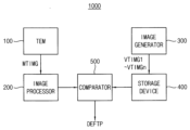
도 1은 본 발명의 실시예들에 따른 크리스탈 결함 분석 시스템을 나타내는 블록도이다.
도 2는 본 발명의 실시예들에 따른 크리스탈 결함 분석 방법을 나타내는 순서도이다.
도 3은 본 발명의 실시예들에 따른 이미지 처리 장치를 나타내는 블록도이다.
도 4는 본 발명의 실시예들에 따른 이미지 처리 방법을 나타내는 순서도이다.
도 5a는 측정 TEM 이미지 및 상응하는 픽셀 데이터를 나타내는 도면이다.
도 5b는 도 5a의 측정 TEM 이미지의 히스토그램을 나타내는 도면이다.
도 6은 도 5a의 측정 TEM 이미지에 대한 본 발명의 실시예들에 따른 커스터마이즈드 히스토그램 등화를 나타내는 도면이다.
도 7은 측정 TEM 이미지 및 이를 히스토그램 등화 처리하여 구해진 등화 이미지의 일 예를 나타내는 도면이다.
도 8은 도 7의 이미지들의 히스토그램들을 나타내는 도면이다.
도 9는 측정 TEM 이미지 및 이를 커스터마이즈드 히스토그램 등화 처리하여 구해진 강화 이미지의 일 예를 나타내는 도면이다.
도 10은 도 9의 이미지들의 히스토그램들을 나타내는 도면이다.
도 11은 본 발명의 실시예들에 따른 결함 라인 검출 방법을 나타내는 순서도이다.
도 12a, 12b, 12c, 12d, 12e 및 12f는 결함 라인 검출 과정을 나타내는 도면들이다.
도 13a, 13b 및 13c는 디스로케이션 코어의 검출 과정에 따른 이미지들을 나타내는 도면들이다.
도 14a 및 14b는 디스로케이션 코어의 위치에 기초한 크롭 이미지를 설명하기 위한 도면들이다.
도 15a 및 15b는 결정 구조 및 원자 배열 방향을 나타내는 도면들이다.
도 16a 및 16b는 본 발명의 실시예들에 따른 가상 TEM 이미지의 발생을 설명하기 위한 도면들이다.
도 17은 측정 TEM 이미지 및 상응하는 가상 TEM 이미지의 예들을 나타내는 도면이다.
도 18은 본 발명의 실시예들에 따른 반도체 공정 개선 방법을 나타내는 순서도이다.
도 19는 본 발명의 실시예들에 따른 컴퓨팅 시스템을 나타내는 블록도이다.1 is a block diagram showing a crystal defect analysis system according to embodiments of the present invention.
Figure 2 is a flowchart showing a crystal defect analysis method according to embodiments of the present invention.
Figure 3 is a block diagram showing an image processing device according to embodiments of the present invention.
Figure 4 is a flowchart showing an image processing method according to embodiments of the present invention.
Figure 5a is a diagram showing the measured TEM image and corresponding pixel data.
FIG. 5B is a diagram showing a histogram of the measured TEM image of FIG. 5A.
FIG. 6 is a diagram showing customized histogram equalization according to embodiments of the present invention for the measured TEM image of FIG. 5A.
Figure 7 is a diagram showing an example of a measured TEM image and an equalized image obtained by histogram equalization processing.
FIG. 8 is a diagram showing histograms of the images of FIG. 7.
Figure 9 is a diagram showing an example of a measured TEM image and an enhanced image obtained by processing it through customized histogram equalization.
FIG. 10 is a diagram showing histograms of the images of FIG. 9.
11 is a flowchart showing a defect line detection method according to embodiments of the present invention.
Figures 12a, 12b, 12c, 12d, 12e, and 12f are diagrams showing the defect line detection process.
Figures 13a, 13b, and 13c are diagrams showing images according to the detection process of the dislocation core.
Figures 14a and 14b are diagrams for explaining a cropped image based on the location of the dislocation core.
Figures 15a and 15b are diagrams showing the crystal structure and atomic arrangement direction.
16A and 16B are diagrams for explaining the generation of virtual TEM images according to embodiments of the present invention.
Figure 17 is a diagram showing examples of measured TEM images and corresponding virtual TEM images.
Figure 18 is a flowchart showing a semiconductor process improvement method according to embodiments of the present invention.
Figure 19 is a block diagram showing a computing system according to embodiments of the present invention.
이하, 첨부한 도면들을 참조하여, 본 발명의 바람직한 실시예를 보다 상세하게 설명하고자 한다. 도면상의 동일한 구성요소에 대해서는 동일한 참조부호를 사용하고 동일한 구성요소에 대해서 중복된 설명은 생략한다.Hereinafter, preferred embodiments of the present invention will be described in more detail with reference to the attached drawings. The same reference numerals are used for the same components in the drawings, and duplicate descriptions for the same components are omitted.
도 1은 본 발명의 실시예들에 따른 크리스탈 결함 분석 시스템을 나타내는 블록도이고, 도 2는 본 발명의 실시예들에 따른 크리스탈 결함 분석 방법을 나타내는 순서도이다.FIG. 1 is a block diagram showing a crystal defect analysis system according to embodiments of the present invention, and FIG. 2 is a flow chart showing a crystal defect analysis method according to embodiments of the present invention.
도 1을 참조하면, 크리스탈 결함 분석 시스템(1000)은 투과 전자 현미경(TEM)(100), 이미지 처리부(200), 이미지 발생부(300), 저장 장치(400) 및 비교부(500)를 포함할 수 있다.Referring to FIG. 1, the crystal
도 1 및 2를 참조하면, 투과 전자 현미경(100)은 크리스탈 구조를 갖는 시료를 촬영하여 측정 TEM 이미지(MTIMG)를 제공할 수 있다(S100). Referring to FIGS. 1 and 2, the
이미지 처리부(200)는 측정 TEM 이미지(MTIMG)를 처리하여 상기 시료의 구조 결함 정보를 제공할 수 있다(S200).The
이미지 발생부(300)는 상기 크리스탈 구조의 복수의 3차원 구조 결함들에 각각 상응하는 복수의 가상 TEM 이미지들(VTIMG1~VTIMGn)을 제공할 수 있다(S300).The
저장 장치(400)는 이미지 발생부(300)로부터 제공되는 복수의 가상 TEM 이미지들(VTIMG1~VTIMGn)을 저장할 수 있다.The
비교부(500)는 상기 구조 결함 정보에 기초하여 측정 TEM 이미지(MTIMG) 및 복수의 가상 TEM 이미지들(VTIMG1~VTIMGn)을 비교하여 측정 TEM 이미지(MTIMG)의 결함 타입을 결정할 수 있다(S400).The
물질의 미세 조직 분석을 위해 최근에는 투과 전자 현미경 (TEM, Transmission Electron Microscope)을 이용한 전자 회절법이 널리 사용되고 있다. 예를 들어, 시료의 나노미터 단위의 미소 영역의 결정 구조, 결함 분포 등을 측정할 수 있는 수렴성 전자빔 회절(CBED, Conversant Beam Electron Diffraction)을 이용하여 측정 TEM 이미지(MTIMG)가 제공될 수 있다. Recently, electron diffraction using a transmission electron microscope (TEM) has been widely used to analyze the microstructure of materials. For example, a measurement TEM image (MTIMG) can be provided using Conversant Beam Electron Diffraction (CBED), which can measure the crystal structure and distribution of defects in nanometer-scale microscopic regions of a sample.
수렴성 전자빔 회절이란 투과 전자 현미경을 이용한 물질의 미세 구조 분석법이다. 전자빔을 대상 시료에 대해 수렴각을 가지도록 조사하여 디스크형 회절 무늬 패턴을 얻는 방법으로, 시료의 두꺼운 부위에서 동력학적인 회절을 통하여 3차원적인 회절을 관찰할 수 있다. 수렴성 전자빔 회절은 공간 분해능이 매우 뛰어나 30nm 정도의 미세한 조직의 결정구조, 격자상수 및 격자 결함 등을 정밀하게 측정할 수 있는 장점이 있다.Convergent electron beam diffraction is a method of analyzing the microstructure of materials using a transmission electron microscope. This is a method of obtaining a disk-shaped diffraction pattern by irradiating an electron beam at a convergence angle to the target sample. Three-dimensional diffraction can be observed through dynamic diffraction in a thick area of the sample. Convergent electron beam diffraction has excellent spatial resolution and has the advantage of being able to precisely measure the crystal structure, lattice constant, and lattice defects of fine structures of about 30 nm.
이미지 처리부(200)는, 도 3 내지 15b를 참조하여 후술하는 바와 같이, 측정 TEM 이미지(MTIMG)보다 콘트라스트가 증가된 강화 이미지를 제공하고, 상기 강화 이미지에 기초하여 원자 배열 패턴을 격자 방향으로 추적하여 상기 원자 배열 패턴의 주기성이 파괴된 결함 픽셀들로 이루어진 결함 라인을 검출하고, 상기 결함 라인의 종점의 위치를 디스로케이션 코어의 위치로 결정할 수 있다. 실시예에 따라서, 이미지 처리부(200)는 측정 TEM 이미지(MTIMG)의 일부 또는 측정 TEM 이미지(MTIMG)에서 노이즈를 제거한 처리 이미지의 일부에 해당하고 상기 디스로케이션 코어의 위치를 중심으로 하고 일정한 사이즈를 갖는 크롭 이미지를 제공할 수 있다.As will be described later with reference to FIGS. 3 to 15B, the
이미지 발생부(300)는, 도 16a 및 16b를 참조하여 후술하는 바와 같이, 전자파가 입사되는 입사 평면을 복수의 도메인들로 분할하고, 각각의 3차원 구조 결함을 상기 입사 평면의 상응하는 위치들에 배치되는 원자들의 각각의 배열로 설정하고, 상기 각각의 3차원 구조 결함에 상응하는 각각의 가상 TEM 이미지의 픽셀 값들을 계산할 수 있다.As will be described later with reference to FIGS. 16A and 16B, the
저장 장치(400)는 복수의 가상 TEM 이미지들(VTIMG1~VTIMGn)을 그대로 비교부(500)에 제공하거나, 복수의 가상 TEM 이미지들(VTIMG1~VTIMGn)을 처리하거나 가공한 이미지들을 비교부(500)에 제공할 수 있다. 실시예에 따라서, 저장 장치(400)는 생략되거나 이미지 발생부(300)에 포함될 수도 있고, 이 경우 복수의 가상 TEM 이미지들(VTIMG1~VTIMGn)은 이미지 발생부(300)로부터 비교부(500)로 직접 제공될 수 있다. The
예를 들어, 저장 장치(400)는 EEPROM(Electrically Erasable Programmable Read-Only Memory), 플래시 메모리(Flash Memory), PRAM(Phase Change Random Access Memory), RRAM(Resistance Random Access Memory), NFGM(Nano Floating Gate Memory), PoRAM(Polymer Random Access Memory), MRAM(Magnetic Random Access Memory), FRAM(Ferroelectric Random Access Memory) 또는 이와 유사한 메모리로 구현될 수 있다.For example, the
검출된 결함의 타입을 분별하기 위해는 리버스 엔지니어링이 필요하다. 3차원 구조에서 발생 가능한 결함 유형은 예를 들어 약 2000개일 수 있으며, 본 발명의 실시예들에 따라서 3차원 구조 결함들을 복수의 가상 TEM 이미지들로 재현할 수 있다. Reverse engineering is necessary to discern the type of defect detected. For example, there may be about 2000 types of defects that can occur in a 3D structure, and according to embodiments of the present invention, 3D structure defects can be reproduced with a plurality of virtual TEM images.
복수의 가상 TEM 이미지 중에서 측정 TEM 이미지와 가장 근사도가 높은 가상 TEM 이미지를 판별하기 위해서 머신 러닝 기법이 이용될 수 있다. 근사도가 높은 이미지들을 판별하기 위해 이미지의 모양을 벡터의 방향성으로 표현한 특징값으로 추출하는 HOG(Histogram Oriented Gradients) 기법과 이를 근사도로 분류하는 SVM(support vector machine), SURF(speeded up robust features), CNN(convolutional neural network) 등의 머신 러닝 기법이 사용될 수 있다.A machine learning technique can be used to determine the virtual TEM image that has the highest degree of approximation to the measured TEM image among a plurality of virtual TEM images. To identify images with a high degree of approximation, the HOG (Histogram Oriented Gradients) technique extracts feature values expressing the shape of the image as the directionality of the vector, and the SVM (support vector machine) and SURF (speeded up robust features) techniques classify them by degree of approximation. , machine learning techniques such as convolutional neural network (CNN) may be used.
비교부(500)는 머신 러닝을 수행하여 상기 복수의 가상 TEM 이미지들 중에서 상기 측정 TEM 이미지와 가장 유사한 매치드 가상 TEM 이미지를 결정할 수 있다. 비교부(500)는 상기 복수의 3차원 구조 결함들 중에서 상기 매치드 가상 TEM 이미지에 상응하는 3차원 구조 결함을 상기 측정 TEM 이미지의 결함 타입으로 결정할 수 있다. The
일 실시예에서, 비교부(500)는 측정 TEM 이미지(MTIMG)의 디스로케이션 코어의 위치 및 복수의 가상 TEM 이미지들(VTIMG1~VTIMGn)의 디스로케이션 코어들의 위치를 일치시켜 측정 TEM 이미지(MTIMG) 및 복수의 가상 TEM 이미지들(VTIMG1~VTIMGn)을 비교할 수 있다. 비교되는 이미지들의 디스로케이션 코어의 위치들을 일치시킴으로써 상기 머신 러닝의 연산량을 현저히 감소시킬 수 있다.In one embodiment, the
이와 같이, 본 발명의 실시예들에 따른 크리스탈 결함 분석 시스템 및 크리스탈 결함 분석 방법은, 이미지 처리 및 결함 검출을 자동화하고 가상 TEM 이미지를 이용한 리버스 엔지니어링을 통하여 3차원 구조 결함의 유형을 분석함으로써 육안 검출시 발생할 수 있는 휴먼 에러를 방지하고 반도체 공정을 효율적으로 평가하고 개선할 수 있다.As such, the crystal defect analysis system and crystal defect analysis method according to embodiments of the present invention automate image processing and defect detection and analyze the type of three-dimensional structural defect through reverse engineering using a virtual TEM image, thereby enabling visual detection. It is possible to prevent human errors that may occur during processing and efficiently evaluate and improve semiconductor processes.
도 3은 본 발명의 실시예들에 따른 이미지 처리 장치를 나타내는 블록도이고, 도 4는 본 발명의 실시예들에 따른 이미지 처리 방법을 나타내는 순서도이다.FIG. 3 is a block diagram showing an image processing device according to embodiments of the present invention, and FIG. 4 is a flowchart showing an image processing method according to embodiments of the present invention.
도 3을 참조하면, 이미지 처리부(200)는 전처리부(210), 결함 라인 검출부(220), 코어 위치 결정부(230) 및 이미지 추출부(240)를 포함할 수 있다.Referring to FIG. 3 , the
도 3 및 4를 참조하면, 전처리부(210)는 측정 TEM 이미지(MTIMG)를 수신하고, 측정 TEM 이미지(MTIMG)보다 콘트라스트가 증가된 강화 이미지를 제공할 수 있다(S210).Referring to FIGS. 3 and 4, the
결함 라인 검출부(220)는 상기 강화 이미지에 기초하여 원자 배열 패턴을 격자 방향으로 추적하여 상기 원자 배열 패턴의 주기성이 파괴된 결함 픽셀들로 이루어진 결함 라인을 검출할 수 있다(S220).The defect
코어 위치 결정부(230)는 상기 결함 라인의 종점의 위치를 디스로케이션 코어의 위치로 결정할 수 있다(S230).The
이미지 추출부(240)는 상기 디스로케이션 코어의 위치를 중심으로 하고 일정한 사이즈를 갖는 크롭 이미지(CRIMG)를 제공할 수 있다(S240).The
전처리부(210)는, 도 5a 내지 10을 참조하여 후술하는 바와 같이, 커스터마이즈드 히스토그램 등화(customized histogram equalization)를 수행하여 상기 강화 이미지를 제공할 수 있다.The
결함 라인 검출부(220)는, 도 11 내지 13c를 참조하여 후술하는 바와 같이, 대각선 방향을 따른 하방 추적 방식으로 하방 패턴 픽셀들을 결정하고, 상기 대각선 방향을 따른 상방 추적 방식으로 상방 패턴 픽셀들을 결정할 수 있다. As described later with reference to FIGS. 11 to 13C, the defect
결함 라인 검출부(220)는 상기 하방 패턴 픽셀들과 상기 상방 패턴 픽셀들 중에서 중복되는 픽셀들을 제외하여 결함 후보 픽셀들을 결정하고, 상기 결함 후보 픽셀들 중에서 기준 개수보다 작은 개수가 서로 연결된 픽셀들을 노이즈 픽셀들로 결정하고, 상기 결함 후보 픽셀들 중에서 상기 노이즈 픽셀들을 제거하여 상기 결함 라인을 결정할 수 있다.The defect
일 실시예에서, 코어 위치 결정부(230)는 상기 결정된 결함 라인의 양 종점들 중에서 이미지의 중심에 가까운 종점의 위치를 디스로케이션 코어의 위치로 결정할 수 있다.In one embodiment, the
이미지 추출부(240)는 측정 TEM 이미지(MTIMG)의 일부를 크롭 이미지(CRIMG)로서 추출하거나 측정 TEM 이미지(MTIMG)에서 노이즈를 제거한 처리 이미지의 일부를 크롭 이미지(CRIMG)로서 추출할 수 있다. The
도 5a는 측정 TEM 이미지 및 상응하는 픽셀 데이터를 나타내는 도면이고, 도 5b는 도 4의 측정 TEM 이미지의 히스토그램을 나타내는 도면이다.FIG. 5A is a diagram showing a measured TEM image and corresponding pixel data, and FIG. 5B is a diagram showing a histogram of the measured TEM image of FIG. 4.
도 5a에는 편의상 실제 TEM 이미지의 일부에 해당하는 8*8(8행 8열) 측정 TEM 이미지(MTIMG1) 및 이에 상응하는 픽셀 데이터(PXD)가 도시되어 있다. 예를 들어, 각 픽셀 값은 8비트 데이터로 표현될 수 있고 이 경우 각 픽셀 값은 0 내지 255의 값을 가질 수 있다.For convenience, Figure 5a shows an 8*8 (8 rows, 8 columns) measured TEM image (MTIMG1) and corresponding pixel data (PXD) corresponding to a portion of the actual TEM image. For example, each pixel value can be expressed as 8-bit data, in which case each pixel value can have a value from 0 to 255.
도 5b에는 도 5a의 픽셀 데이터(PXD)의 각 픽셀 값(v) 및 픽셀 값(v)을 갖는 픽셀들의 개수 또는 빈도수(c(v))에 대한 히스토그램이 도시되어 있다.FIG. 5B shows a histogram for each pixel value (v) of the pixel data (PXD) of FIG. 5A and the number or frequency (c(v)) of pixels having the pixel value (v).
도 6은 도 4의 측정 TEM 이미지에 대한 본 발명의 실시예들에 따른 커스터마이즈드 히스토그램 등화를 나타내는 도면이다.FIG. 6 is a diagram showing customized histogram equalization according to embodiments of the present invention for the measured TEM image of FIG. 4.
도 6에서 v는 픽셀 값을 나타내고, cdf(v)는 c(0) 부터 c(v)를 합산한 누적 빈도수를 나타내고, h(v)는 노말 히스토그램 등화를 수행하여 구해진 등화 픽셀 값을 나타내고, ch(v)는 커스터마이즈드 히스토그램 등화를 수행하여 구해진 커스터마이즈드 픽셀 값, 즉 강화 이미지의 픽셀 값을 나타낸다.In Figure 6, v represents the pixel value, cdf(v) represents the cumulative frequency summing c(0) to c(v), h(v) represents the equalized pixel value obtained by performing normal histogram equalization, ch(v) represents the customized pixel value obtained by performing customized histogram equalization, that is, the pixel value of the enhanced image.
도 6에 도시된 커스터마이즈드 픽셀 값(ch(v))은 하기의 수학식 1 내지 3을 이용하여 구할 수 있다.The customized pixel value (ch(v)) shown in FIG. 6 can be obtained using
[수학식 1][Equation 1]
[수학식 2][Equation 2]
[수학식 3][Equation 3]
수학식 1 내지 3에서, RND()는 반올림, 내림 또는 올림 함수를 나타내고, M은 이미지의 행의 수를 나타내고, N은 이미지의 열의 수를 나타내고, cdf(v)는 0부터 v까지의 빈도수를 합산한 누적 빈도수를 나타내고, cdfmin은 최소 누적 빈도수를 나타내고, vmax는 최대 픽셀 값을 나타내고, CV1은 제1 조정 값을 나타내고, CV2는 제2 조정 값을 나타내고, tv1은 제1 문턱 빈도수를 나타내고, tv2는 제2 문턱 빈도수를 나타낸다.In
수학식 1 내지 3에서 CV1=CV2=0으로 설정된 경우 등화 픽셀 값(h(v))과 커스터마이즈드 픽셀 값(ch(v))은 동일하게 된다.When CV1=CV2=0 is set in
제1 조정 값(CV1) 및 제2 조정 값(CV2)은 캘리브레이션 과정을 통해 결정될 수 있으며, 예를 들어, 제1 조정 값(CV1) 및 제2 조정 값(CV2)은 최대 픽셀 값(vmax)의 약 10% 이내로 제한될 수 있다. 제1 문턱 빈도수(tv1) 및 제2 문턱 빈도수(tv2)는 총 픽셀 개수(M×N)의 일정한 비율 예를 들어 약 20% 이내로 설정될 수 있다.The first adjustment value (CV1) and the second adjustment value (CV2) may be determined through a calibration process. For example, the first adjustment value (CV1) and the second adjustment value (CV2) are the maximum pixel value (v max) . ) may be limited to approximately 10% of The first threshold frequency (tv1) and the second threshold frequency (tv2) may be set within a certain ratio, for example, about 20% of the total number of pixels (M×N).
이와 같은 커스터마이즈드 히스토그램 등화를 통하여 일부의 하위 픽셀 값들(PXL)을 더욱 작게 감소하고 일부의 상위 픽셀 값들(PXH)을 더욱 크게 증가함으로써 TEM 이미지의 콘트라스트를 더욱 증가시킬 수 있다.Through such customized histogram equalization, the contrast of the TEM image can be further increased by further reducing some of the lower pixel values (PXL) and increasing some of the upper pixel values (PXH) to a greater extent.
도 6의 예는 vmax=255, CV1=25, CV2=10, tv1=10, tv2=52의 값을 적용한 경우를 나타낸다.The example in FIG. 6 shows a case where the values v max = 255, CV1 = 25, CV2 = 10, tv1 = 10, and tv2 = 52 are applied.
도 7은 측정 TEM 이미지 및 이를 히스토그램 등화 처리하여 구해진 등화 이미지의 일 예를 나타내는 도면이고, 도 8은 도 7의 이미지들의 히스토그램들을 나타내는 도면이다.FIG. 7 is a diagram illustrating an example of a measured TEM image and an equalized image obtained by histogram equalization processing, and FIG. 8 is a diagram illustrating histograms of the images of FIG. 7 .
도 7을 참조하면, 측정 TEM 이미지(MTIMG1)은 측정된 본래의 픽셀 값들(v)을 갖고, 측정 TEM 이미지(MTIMG1)에 대해 노말 히스토그램 등화를 수행하여 구해진 등화 이미지(IMG11)는 전술한 바와 같은 등화 픽셀 값들(h(v))을 갖는다.Referring to FIG. 7, the measured TEM image (MTIMG1) has the original measured pixel values (v), and the equalized image (IMG11) obtained by performing normal histogram equalization on the measured TEM image (MTIMG1) is as described above. It has equalized pixel values (h(v)).
도 8을 참조하면, 측정 TEM 이미지(MTIMG1)의 히스토그램(HST1)과 비교하여 등화 이미지(IMG11)의 히스토그램(HST11)은 픽셀 값들의 산포도가 증가한다. 결과적으로 측정 TEM 이미지(MTIMG1)와 비교하여 등화 이미지(IMG11)의 콘트라스트가 증가한다.Referring to FIG. 8, compared to the histogram HST1 of the measurement TEM image MTIMG1, the histogram HST11 of the equalization image IMG11 has an increased dispersion of pixel values. As a result, the contrast of the equalization image (IMG11) increases compared to the measurement TEM image (MTIMG1).
도 9는 측정 TEM 이미지 및 이를 커스터마이즈드 히스토그램 등화 처리하여 구해진 강화 이미지의 일 예를 나타내는 도면이고, 도 10은 도 9의 이미지들의 히스토그램들을 나타내는 도면이다.FIG. 9 is a diagram illustrating an example of a measured TEM image and an enhanced image obtained by performing customized histogram equalization processing, and FIG. 10 is a diagram illustrating histograms of the images of FIG. 9 .
도 9를 참조하면, 측정 TEM 이미지(MTIMG2)은 측정된 본래의 픽셀 값들(v)을 갖고, 측정 TEM 이미지(MTIMG2)에 대해 커스터마이즈드 히스토그램 등화를 수행하여 구해진 강화 이미지(IMG22)는 전술한 바와 같은 커스터마이즈드 픽셀 값들(ch(v))을 갖는다.Referring to FIG. 9, the measured TEM image (MTIMG2) has the original measured pixel values (v), and the enhanced image (IMG22) obtained by performing customized histogram equalization on the measured TEM image (MTIMG2) is as described above. It has the same customized pixel values (ch(v)).
도 10에는 상응하는 누적 빈도수(cdf)가 함께 도시되어 있다. 도 10을 참조하면, 측정 TEM 이미지(MTIMG2)의 히스토그램(HST2)과 비교하여 강화 이미지(IMG22)의 히스토그램(HST22)은 픽셀 값들의 산포도가 더욱 증가한다. 결과적으로 측정 TEM 이미지(MTIMG2)와 비교하여 강화 이미지(IMG22)의 콘트라스트가 더욱 증가한다.In Figure 10, the corresponding cumulative frequency (cdf) is also shown. Referring to FIG. 10, compared to the histogram (HST2) of the measured TEM image (MTIMG2), the histogram (HST22) of the enhanced image (IMG22) has a further increase in the dispersion of pixel values. As a result, the contrast of the enhanced image (IMG22) is further increased compared to the measured TEM image (MTIMG2).
이와 같이, 등화 픽셀 값들(h(v))을 더욱 강화하여 구해진 커스터마이즈드 픽셀 값들(ch(v))은 일부의 하위 픽셀 값들을 더욱 작게 감소시키고 일부의 상위 픽셀 값들을 더욱 크게 증가시킨 것이다. 이러한 커스터마이즈드 픽셀 값들(ch(v))로 이루어진 강화 이미지는 어두운 부분은 더욱 어둡게 되고 밝은 부분은 더욱 밝게 되어 원자의 배열 패턴을 효율적으로 추적할 수 있다.In this way, the customized pixel values (ch(v)) obtained by further strengthening the equalization pixel values (h(v)) further reduce some lower pixel values to a smaller size and further increase some upper pixel values. The enhanced image composed of these customized pixel values (ch(v)) becomes darker in dark areas and brighter in bright areas, making it possible to efficiently track the arrangement pattern of atoms.
도 11은 본 발명의 실시예들에 따른 결함 라인 검출 방법을 나타내는 순서도이다.11 is a flowchart showing a defect line detection method according to embodiments of the present invention.
도 11을 참조하면, 도 3의 이미지 처리부(200)에 포함되는 결함 라인 검출부(220)는 대각선 방향을 따른 하방 추적 방식으로 하방 패턴 픽셀들을 결정하고(S221), 상기 대각선 방향을 따른 상방 추적 방식으로 상방 패턴 픽셀들을 결정한다(S222). Referring to FIG. 11, the defect
결함 라인 검출부(220)는 상기 하방 패턴 픽셀들과 상기 상방 패턴 픽셀들 중에서 중복되는 픽셀들을 제외하여 결함 후보 픽셀들을 결정하고(S223), 상기 결함 후보 픽셀들 중에서 기준 개수보다 작은 개수가 서로 연결된 픽셀들을 노이즈 픽셀들로 결정할(S224) 수 있다. 결함 라인 검출부(220)는 상기 결함 후보 픽셀들 중에서 상기 노이즈 픽셀들을 제거하여 상기 결함 라인을 결정할 수 있다.The defect
이하, 예시적인 측정 TEM 이미지를 기초로 전술한 결함 라인 검출 방법을 설명한다.Hereinafter, the above-described defect line detection method will be described based on exemplary measurement TEM images.
도 12a, 12b, 12c, 12d, 12e 및 12f는 결함 라인 검출 과정을 나타내는 도면들이다.Figures 12a, 12b, 12c, 12d, 12e, and 12f are diagrams showing the defect line detection process.
도 12a에는 측정 TEM 이미지를 전술한 바와 같이 커스터마이즈드 등화 처리하여 구해진 강화 이미지가 도시되어 있다. 도 12a의 강화 이미지는 실제로 측정된 TEM 이미지의 일부분에 해당한다.Figure 12a shows an enhanced image obtained by customizing the measured TEM image as described above. The enhanced image in Figure 12a corresponds to a portion of the actually measured TEM image.
도 12b에는 대각선 방향을 따른 하방 추적 방식으로 결정된 하방 패턴 픽셀들이 색칠된 픽셀들로 표시되어 있다. In Figure 12b, downward pattern pixels determined by downward tracking along the diagonal direction are displayed as colored pixels.
일 실시예에서, 도 12b에 도시된 바와 같이, 좌하방 추적 방식으로 하방 패턴 픽셀들이 결정될 수 있다. 다시 말해, p번째 하방 패턴 픽셀의 좌표가 (X, Y)일 때 (X+1, Y), (X, Y-1) 및 (X+1, Y-1) 중에서 최대 픽셀 값에 상응하는 좌표를 p+1번째 하방 패턴 픽셀의 좌표로 결정할 수 있다. 여기서, X는 픽셀의 행 좌표(R1~R20)이고 Y는 픽셀의 열 좌표(C1~C20)를 나타낸다.In one embodiment, as shown in FIG. 12B, downward pattern pixels may be determined using a downward-left tracking method. In other words, when the coordinates of the pth downward pattern pixel are (X, Y), the maximum pixel value among (X+1, Y), (X, Y-1) and (X+1, Y-1) is The coordinates can be determined as the coordinates of the p+1th downward pattern pixel. Here, X represents the row coordinates of the pixel (R1 to R20) and Y represents the column coordinates of the pixel (C1 to C20).
예를 들어, (R1, C10)이 p번째 하방 패턴 픽셀일 때, (R2, C10), (R1, C9), (R2, C9) 중에서 최대 픽셀 값인 115에 상응하는 (R2, C10)을 p+1번째 하방 패턴 픽셀의 좌표로 결정할 수 있다. For example, when (R1, C10) is the p-th downward pattern pixel, (R2, C10) corresponding to the maximum pixel value of 115 among (R2, C10), (R1, C9), and (R2, C9) is p. It can be determined by the coordinates of the +1th downward pattern pixel.
다시 (R2, C10)이 p+1번째 하방 패턴 픽셀일 때, (R3, C10), (R2, C9), (R3, C9) 중에서 최대 픽셀 값인 81에 상응하는 (R2, C9)을 p+2번째 하방 패턴 픽셀의 좌표로 결정할 수 있다. Again, when (R2, C10) is the p+1th downward pattern pixel, (R2, C9) corresponding to the maximum pixel value of 81 among (R3, C10), (R2, C9), and (R3, C9) is p+ It can be determined by the coordinates of the second downward pattern pixel.
이와 같은 방식으로 마지막 행에 도달할 때까지 좌하의 대각선 방향으로 추적하여 하방 패턴 픽셀들을 결정할 수 있다. 도 12b에 도시된 다수의 라인들은 복수의 씨드 픽셀들에서부터 각각 좌하방 추적 방식이 수행된 것을 나타낸다. 상기 씨드 픽셀들은 전체 이미지의 첫번째 행의 픽셀 값들 및 일정한 기준에 기초하여 결정될 수 있다.In this way, the downward pattern pixels can be determined by tracing diagonally in the lower left direction until the last row is reached. Multiple lines shown in FIG. 12B indicate that the left-down tracking method is performed from a plurality of seed pixels, respectively. The seed pixels may be determined based on pixel values of the first row of the entire image and a certain standard.
도 12c에는 대각선 방향을 따른 상방 추적 방식으로 결정된 상방 패턴 픽셀들이 굵은 사각형으로 표시된 픽셀들로 표시되어 있다. In Figure 12c, the upward pattern pixels determined by the upward tracking method along the diagonal direction are indicated as pixels indicated by bold squares.
일 실시예에서, 도 12c에 도시된 바와 같이, 우상방 추적 방식으로 상방 패턴 픽셀들이 결정될 수 있다. 다시 말해, s번째 상방 패턴 픽셀의 좌표가 (X, Y)일 때 (X-1, Y), (X, Y+1) 및 (X-1, Y+1) 중에서 최대 픽셀 값에 상응하는 좌표를 s+1번째 상방 패턴 픽셀의 좌표로 결정할 수 있다. 여기서, X는 픽셀의 행 좌표(R1~R20)이고 Y는 픽셀의 열 좌표(C1~C20)를 나타낸다.In one embodiment, as shown in FIG. 12C, upward pattern pixels may be determined using an upward-right tracking method. In other words, when the coordinates of the sth upper pattern pixel are (X, Y), the corresponding pixel value among (X-1, Y), (X, Y+1) and (X-1, Y+1) is The coordinates can be determined as the coordinates of the s+1th upper pattern pixel. Here, X represents the row coordinates of the pixel (R1 to R20) and Y represents the column coordinates of the pixel (C1 to C20).
예를 들어, (R20, C2)이 s번째 상방 패턴 픽셀일 때, (R19, C2), (R20, C3), (R19, C3) 중에서 최대 픽셀 값인 70에 상응하는 (R19, C2)을 s+1번째 상방 패턴 픽셀의 좌표로 결정할 수 있다. For example, when (R20, C2) is the sth upper pattern pixel, (R19, C2) corresponding to the maximum pixel value of 70 among (R19, C2), (R20, C3), and (R19, C3) is selected for s. It can be determined by the coordinates of the +1th upper pattern pixel.
다시 (R19, C2)이 s+1번째 상방 패턴 픽셀일 때, (R18, C2), (R19, C3), (R18, C3) 중에서 최대 픽셀 값인 70에 상응하는 (R18, C3)을 s+2번째 상방 패턴 픽셀의 좌표로 결정할 수 있다. Again, when (R19, C2) is the s+1th upper pattern pixel, (R18, C3) corresponding to the maximum pixel value of 70 among (R18, C2), (R19, C3), and (R18, C3) is added to s+ It can be determined by the coordinates of the second upper pattern pixel.
이와 같은 방식으로 첫번째 행에 도달할 때까지 우상의 대각선 방향으로 추적하여 상방 패턴 픽셀들을 결정할 수 있다. 도 12c에 도시된 다수의 라인들은 복수의 씨드 픽셀들에서부터 각각 우상방 추적 방식이 수행된 것을 나타낸다. 상기 씨드 픽셀들은 전체 이미지의 마지막 행의 픽셀 값들 및 일정한 기준에 기초하여 결정될 수 있다.In this way, the upper pattern pixels can be determined by tracing diagonally to the upper right until the first row is reached. The multiple lines shown in FIG. 12C indicate that the upper right tracking method has been performed from a plurality of seed pixels, respectively. The seed pixels may be determined based on pixel values of the last row of the entire image and a certain standard.
도 12b 및 도 12c를 참조하여 좌하방 추적 방식으로 하방 패턴 픽셀들을 결정하고 우상방 추적 방식으로 상방 패턴 픽셀들을 결정하는 실시예를 설명하였으나, 본 발명의 실시예들이 이에 한정되는 것을 아니다. 다른 실시예에서, 우하방 추적 방식에 따라서 하방 패턴 픽셀들이 결정되고, 좌상방 추적 방식에 따라서 상방 패턴 픽셀들이 결정될 수 있다. 즉, 우하방 추적 방식에 따라서, p번째 하방 패턴 픽셀의 좌표가 (X, Y)일 때 (X+1, Y), (X, Y+1) 및 (X+1, Y+1) 중에서 최대 픽셀 값에 상응하는 좌표를 p+1번째 하방 패턴 픽셀의 좌표로 결정할 수 있고, 좌상방 추적 방식에 따라서, s번째 상방 패턴 픽셀의 좌표가 (X, Y)일 때 (X-1, Y), (X, Y-1) 및 (X-1, Y-1) 중에서 최대 픽셀 값에 상응하는 좌표를 s+1번째 상방 패턴 픽셀의 좌표로 결정할 수 있다.An embodiment of determining downward pattern pixels using a downward left tracking method and determining upward pattern pixels using an upward right tracking method has been described with reference to FIGS. 12B and 12C , but embodiments of the present invention are not limited thereto. In another embodiment, downward pattern pixels may be determined according to a downward-right tracking method, and upward pattern pixels may be determined according to an upward-left tracking method. That is, according to the downward right tracking method, when the coordinates of the pth downward pattern pixel are (X, Y), among (X+1, Y), (X, Y+1) and (X+1, Y+1) The coordinates corresponding to the maximum pixel value can be determined as the coordinates of the p+1th downward pattern pixel, and according to the upper left tracking method, when the coordinates of the sth upper pattern pixel are (X, Y), (X-1, Y ), (X, Y-1), and (X-1, Y-1), the coordinate corresponding to the maximum pixel value can be determined as the coordinate of the s+1th upper pattern pixel.
도 12d에는 도 12b 및 12c에 설명한 바와 같이 결정된 하방 패턴 픽셀들 및 상방 패턴 픽셀들이 함께 표시되어 있다. In FIG. 12D, downward pattern pixels and upward pattern pixels determined as described in FIGS. 12B and 12C are displayed together.
상기 하방 패턴 픽셀들과 상기 상방 패턴 픽셀들 중에서 중복되는 픽셀들을 제외하여 결함 후보 픽셀들을 결정할 수 있다. 즉, 하방 패턴 픽셀이면서 상방 패턴 픽셀이 아닌 경우 및 상방 패턴 픽셀이면서 하방 패턴 픽셀이 아닌 경우 결함 후보 픽셀로 결정될 수 있다. Defect candidate pixels may be determined by excluding overlapping pixels among the downward pattern pixels and the upward pattern pixels. That is, when a pixel is a downward pattern pixel but not an upward pattern pixel, and when it is an upward pattern pixel but not a downward pattern pixel, it may be determined as a defect candidate pixel.
도 12e에는 전술한 바와 같이 결정된 결함 후보 픽셀들이 도시되어 있다. 도 12e에 도시된 바와 같이 결함 후보 픽셀들 이외의 픽셀들의 값은 모두 0으로 치환될 수 있다. 상기 결함 후보 픽셀들 중에서 기준 개수보다 작은 개수가 서로 연결된 하방 패턴 픽셀들 및 상기 기준 개수보다 작은 개수가 서로 연결된 상기 하방 패턴들을 노이즈 픽셀들로 결정할 수 있다.FIG. 12E shows defect candidate pixels determined as described above. As shown in FIG. 12E, the values of pixels other than defect candidate pixels may all be replaced with 0. Among the defect candidate pixels, downward pattern pixels with a smaller number than the reference number connected to each other and the lower pattern pixels with a smaller number than the reference number connected with each other may be determined as noise pixels.
예를 들어, 도 12e의 결함 후보 픽셀들에 대하여 상기 기준 개수를 15로 적용하면 (R20, C9)부터 (R7, C16)을 종점들로 하여 서로 연결된 하방 패턴 픽셀들을 제외한 결함 후보 픽셀들은 노이즈 픽셀들로 결정된다.For example, if the reference number is applied to the defect candidate pixels of FIG. 12E as 15, the defect candidate pixels excluding the downward pattern pixels connected to each other with end points from (R20, C9) to (R7, C16) are noise pixels. It is decided by
도 12f에는 결함 라인을 형성하는 결함 픽셀들이 도시되어 있다. 도 12e의 결함 후보 픽셀들 중에서 전술한 바와 같이 결정된 노이즈 픽셀들을 제거하여 상기 결함 라인을 형성하는 결함 픽셀들을 결정할 수 있다. 도 12f에 도시된 바와 같이 결함 픽셀 이외의 픽셀들은 모두 0의 값으로 치환될 수 있다. FIG. 12F shows defective pixels forming a defect line. The defective pixels forming the defect line can be determined by removing the noise pixels determined as described above from among the defect candidate pixels of FIG. 12E. As shown in FIG. 12F, all pixels other than defective pixels may be replaced with a value of 0.
도 3의 코어 위치 결정부(230)는 상기 결함 라인의 종점의 위치를 디스로케이션 코어의 위치로 결정할 수 있다. 일 실시예에서, 코어 위치 결정부(230)는 상기 결정된 결함 라인의 양 종점들 중에서 이미지의 중심에 가까운 종점의 위치를 디스로케이션 코어의 위치로 결정할 수 있다. 도 12f의 경우에, 코어 위치 결정부(230)는 (R7, C16)의 좌표를 디스로케이션 코어의 위치로 결정할 수 있다.The
도 13a, 13b 및 13c는 디스로케이션 코어의 검출 과정에 따른 이미지들을 나타내는 도면들이다.Figures 13a, 13b, and 13c are diagrams showing images according to the detection process of the dislocation core.
도 13a에는 전술한 결함 후보 픽셀들에 상응하는 제1 이미지(IMG1)가 도시되어 있고, 도 13b에는 제1 이미지(IMG1)에서 1개 또는 2개의 결함 후보 픽셀들이 연결된 노이즈 픽셀들을 0의 값으로 치환한 제2 이미지(IMG2)가 도시되어 있다. 제2 이미지(IMG2)에서 전술한 바와 같은 기준 개수에 기초한 연결도(connectivity)를 고려하여 추가적인 노이즈 픽셀들을 제거함으로써 도 13c에 도시된 바와 같은 결함 라인을 검출할 수 있다.In FIG. 13A, a first image (IMG1) corresponding to the above-described defect candidate pixels is shown, and in FIG. 13B, noise pixels to which one or two defect candidate pixels are connected in the first image (IMG1) are set to a value of 0. A replaced second image (IMG2) is shown. A defect line as shown in FIG. 13C can be detected by removing additional noise pixels in the second image IMG2 by considering the connectivity based on the reference number as described above.
도 14a 및 14b는 디스로케이션 코어의 위치에 기초한 크롭 이미지를 설명하기 위한 도면들이다.Figures 14a and 14b are diagrams for explaining a cropped image based on the location of the dislocation core.
도 14a를 참조하면, 크롭 이미지(CTIMG) 및 가상 TEM 이미지(VTIMG)는 동일한 사이즈를 가질 수 있다. 즉 크롭 이미지(CTIMG)의 행 사이즈(HGT1)는 가상 TEM 이미지(VTIMG)의 행 사이즈(HGT2)와 동일하고, 크롭 이미지(CTIMG)의 열 사이즈(WDT1)는 가상 TEM 이미지(VTIMG)의 열 사이즈(WDT2)와 동일할 수 있다.Referring to FIG. 14A, the crop image (CTIMG) and the virtual TEM image (VTIMG) may have the same size. That is, the row size (HGT1) of the cropped image (CTIMG) is the same as the row size (HGT2) of the virtual TEM image (VTIMG), and the column size (WDT1) of the cropped image (CTIMG) is the column size of the virtual TEM image (VTIMG). It may be the same as (WDT2).
전술한 바와 같이, 크롭 이미지(CRIMG)는 상기 측정 TEM 이미지의 일부 또는 상기 측정 TEM 이미지에서 노이즈를 제거한 처리 이미지의 일부에 해당하고 디스로케이션 코어의 위치(Pdc)를 중심으로 하고 일정한 사이즈를 가질 수 있다. 한편, 도 16a 및 16b를 참조하여 후술하는 가상 TEM 이미지들의 발생시 각각의 3차원 구조 결함의 디스로케이션 코어(Porg)가 입사 평면의 중앙에 위치하도록 상기 원자들을 배열할 수 있다.As described above, the cropped image (CRIMG) corresponds to a part of the measured TEM image or a part of a processed image in which noise has been removed from the measured TEM image, is centered on the position (Pdc) of the dislocation core, and may have a constant size. there is. Meanwhile, when generating virtual TEM images, which will be described later with reference to FIGS. 16A and 16B, the atoms may be arranged so that the dislocation core (Porg) of each 3D structural defect is located at the center of the incident plane.
이와 같이, 측정 TEM 이미지의 디스로케이션 코어의 위치(Pdc) 및 복수의 가상 TEM 이미지들의 디스로케이션 코어들의 위치(Porg)를 일치시켜 상기 측정 TEM 이미지 및 상기 복수의 가상 TEM 이미지들을 비교할 수 있다.In this way, the measured TEM image and the plurality of virtual TEM images can be compared by matching the position (Pdc) of the dislocation core in the measured TEM image and the position (Porg) of the dislocation cores in the plurality of virtual TEM images.
비교되는 이미지들의 디스로케이션 코어의 위치 및 사이즈를 일치시킴으로써, 이미지 매칭을 위한 연산량을 현저히 감소시킬 수 있다.By matching the positions and sizes of the dislocation cores of compared images, the amount of computation for image matching can be significantly reduced.
도 15a 및 15b는 결정 구조 및 원자 배열 방향을 나타내는 도면들이다.Figures 15a and 15b are diagrams showing the crystal structure and atomic arrangement direction.
일반적으로 공정 분석에 사용하는 TEM 이미지는 {110} 평면으로 촬영될 수 있다. 이때 X 축은 <110> 방향이고, Y 축은 <001> 방향이 된다. Si 는 도 15a에 도시된 바와 같은 큐빅 다이아몬드(Cubic Diamond) 격자 구조이고, 이를 X축 <110>, Y축 <001> 방향이 되도록 놓으면 도 15b에 도시된 바와 같이 <112> 방향으로 규칙적인 원자 배열이 관찰되는데, <112> 방향과 X축 <110> 방향의 각도가 54.7o 가 된다.Generally, TEM images used for process analysis can be taken in the {110} plane. At this time, the X axis is in the <110> direction and the Y axis is in the <001> direction. Si has a cubic diamond lattice structure as shown in Figure 15a, and when placed in the X-axis <110> and Y-axis <001> directions, regular atoms are formed in the <112> direction as shown in Figure 15b The arrangement is observed, and the angle between the <112> direction and the X-axis <110> direction is 54.7o.
도 11 내지 12f를 참조하여 설명한 본 발명의 격자 방향(lattice direction)의 이미지 트레이싱(image tracing) 기법은 공정 분석에 사용하는 TEM 이미지 촬영 평면에서, Si 격자 구조의 특징적인 배열이 나타나는 54.7o 와 35.3o 방향의 주기성을 검사하는데 효율적이다. The image tracing technique of the lattice direction of the present invention described with reference to FIGS. 11 to 12f shows the characteristic arrangement of the Si lattice structure at 54.7o and 35.3 in the TEM imaging plane used for process analysis. o It is efficient in checking the periodicity of direction.
디스로케이션 코어의 주변부는 격자의 주기성이 국부적으로 어긋난(locally dislocated) 것이 특징이다. 디스로케이션이 발생하기 위해서는 원자 배열의 일부가 동일하게 트랜슬레이션(translation) 해야 하고, 이러한 트랜슬레이션 벡터를 버거스 벡터(Burgers vector)라고 한다. 이때 에너지적으로 가장 안정한 최소 격자 트랜슬레이션(minimum lattice translation)을 나타내는 버거스 벡터는 1/6<112>이 된다. 즉, <112> 방향 (일반적인 공정 분석 TEM 에서 X축과 54.7o 대각선 방향)의 주기성을 비교하는 것이 디스로케이션 코어를 찾는 효율적인 방법이 된다.The periphery of the dislocation core is characterized by locally dislocated lattice periodicity. In order for dislocation to occur, part of the atomic arrangement must be translated identically, and this translation vector is called a Burgers vector. At this time, the Burgers vector representing the energetically most stable minimum lattice translation is 1/6<112>. In other words, comparing the periodicity of the <112> direction (diagonal direction of 54.7° with the X axis in a general process analysis TEM) is an efficient way to find the dislocation core.
도 16a 및 16b는 본 발명의 실시예들에 따른 가상 TEM 이미지의 발생을 설명하기 위한 도면들이다.16A and 16B are diagrams for explaining the generation of virtual TEM images according to embodiments of the present invention.
도 16a를 참조하면, 전자빔 또는 전자파가 입사되는 입사 평면을 복수의 도메인들로 분할할 수 있다. 각각의 3차원 구조 결함을 상기 입사 평면의 상응하는 위치들에 배치되는 원자들의 각각의 배열로 설정할 수 있다. 도 16a에는 도시의 편의상 하나의 도메인에 배치되는 하나의 원자만을 도시하였으나, 각각의 도메인마다 하나의 원자가 배치될 수 있다.Referring to FIG. 16A, the incident plane where the electron beam or electromagnetic wave is incident can be divided into a plurality of domains. Each three-dimensional structural defect can be set to a respective arrangement of atoms placed at corresponding positions in the plane of incidence. In FIG. 16A, only one atom is shown in one domain for convenience of illustration, but one atom may be placed in each domain.
멀티-슬라이스(multi-slice) 방법은 시간이 오래 걸려 최소 수nm에서 수백nm에 이르는 실제 시료를 모사하는데 사용할 수 없어서 실제 계산을 근사화 하는 방법이 필요하다. 멀티-슬라이스 방법은 전자파의 진행을, 아주 잘게 쪼갠 슬라이스들(또는 슬릿들)을 통과하는 모델로 계산함으로써 계산량이 매우 증가한다. The multi-slice method takes a long time and cannot be used to simulate actual samples ranging from at least a few nm to hundreds of nm, so a method to approximate the actual calculation is needed. The multi-slice method greatly increases the amount of calculation by calculating the propagation of electromagnetic waves using a model that passes through very finely divided slices (or slits).
본 발명의 실시예들에 따라서, 전자파가 진행하면서 발생하는 모든 이차적인 산란(secondary scattering)을 무시하여, 계산량을 획기적으로 줄이고, 최종적으로 투과한 빛의 세기(intensity)만으로 TEM 이미지를 모사할 수 있다. According to embodiments of the present invention, by ignoring all secondary scattering that occurs as electromagnetic waves progress, the amount of calculations can be dramatically reduced, and a TEM image can be simulated using only the intensity of the final transmitted light. there is.
빛의 진행 방향을 Z 방향이라고 하면, 본 발명의 실시예들에 따른 근사 방법에서는 멀티-슬라이스 방법과 달리 각 원자 위치 에 따른 원자 포텐셜(atomic potential)을 2차원 (z=0) 평면에 중첩시켜 통과시킨다. 종래의 멀티-슬라이스 방법과 달리 z=0인 x-y 평면을 한번만 통과하므로 이차적인 산란은 모두 무시된다. 빛은 이 x-y 평면을 잘게 쪼갠 (domain-decomposition) 각 원자 위치 를 통과하면서 이 x-y 평면에 배치된 원자 포텐셜에 의해 산란하는 것으로 모사할 수 있다. If the direction of light travel is the Z direction, in the approximation method according to embodiments of the present invention, unlike the multi-slice method, the atomic potential according to each atomic position is superimposed on the two-dimensional (z = 0) plane. Let it pass. Unlike the conventional multi-slice method, since it passes through the x-y plane at z=0 only once, all secondary scattering is ignored. Light can be simulated by dividing this x-y plane into small pieces (domain-decomposition) and passing through each atomic position and being scattered by the atomic potential placed on this x-y plane.
이때 입사하는 빛은 단파장 빔(monochromatic beam)으로 가정, 즉 빛의 파장에 따른 변동(variation)이 없는 정현 평면파(sinusoidal plane wave)라고 가정한다.At this time, the incident light is assumed to be a monochromatic beam, that is, it is assumed to be a sinusoidal plane wave with no variation depending on the wavelength of the light.
또한 파동을 시간에 따라 평균하는 (time-averaged) 것으로 가정하여 시간에 따른 위상 변동(phase variation)은 없다고 가정한다. 이러한 가정을 통해 빛의 세기(intensity), 즉 빛의 방사(irradiation)를 시간 평균된 방사 에너지 플럭스(time-averaged radiated energy flux)의 양으로서 표현하고, 이는 수학식 4에 표현된 바와 같이 포인팅 벡터(Poynting vector)의 실수부 에 해당된다.Additionally, it is assumed that the waves are time-averaged and that there is no phase variation over time. Through these assumptions, the intensity of light, that is, the irradiation of light, is expressed as the amount of time-averaged radiated energy flux, which is the Poynting vector as expressed in
[수학식 4][Equation 4]
빛의 세기가 공간상에서 어떻게 분포하는지는 각각의 잘게 쪼개진 도메인에서 원자 포텐셜에 산란되어 손실된 세기로 표현하면 수학식 5와 같다.How the intensity of light is distributed in space can be expressed as the intensity lost by scattering to the atomic potential in each finely divided domain, as shown in
[수학식 5][Equation 5]
수학식 5에서 이고, 도 16b에 도시된 바와 같이 은 가상 TEM 이미지 상의 픽셀의 위치 벡터이고 은 원자의 위치 벡터이다.In equation 5: , and as shown in Figure 16b is the position vector of the pixel on the virtual TEM image and is the position vector of the atom.
빛의 진행 방향에 대하여 z=0으로 고정하면, 수학식 5는 z에 무관하게 되고, 결과적으로 수학식 6과 같이 간소화될 수 있다.If z = 0 is fixed for the direction of light travel,
[수학식 6][Equation 6]
수학식 6에서, A는 제1 파라미터이고 B는 제2 파라미터이고, 각각의 가상 TEM 이미지가 실제 TEM 이미지에 근접하도록 하기 위한 튜닝 과정을 통하여 상기 제1 파라미터(A) 및 상기 제2 파라미터(B)가 결정될 수 있다.In
결과적으로, 각각의 3차원 구조 결함에 상응하는 각각의 가상 TEM 이미지의 픽셀 값들은 수학식 7과 같이 모든 원자들에 의한 빛의 세기를 합산함으로써 구할 수 있다.As a result, the pixel values of each virtual TEM image corresponding to each 3D structural defect can be obtained by summing the light intensity from all atoms as shown in Equation 7.
[수학식 7][Equation 7]
수학식 7에서, 은 각각의 가상 TEM 이미지 상의 픽셀의 위치 벡터를 나타내고, 은 원자의 위치 벡터를 나타내고, 은 에서의 픽셀 값을 나타내고, A는 제1 파라미터를 나타내고, B는 제2 파라미터를 나타낸다.In equation 7, represents the position vector of the pixel on each virtual TEM image, represents the position vector of the atom, silver represents the pixel value in, A represents the first parameter, and B represents the second parameter.
도 17은 측정 TEM 이미지 및 상응하는 가상 TEM 이미지의 예들을 나타내는 도면이다.Figure 17 is a diagram showing examples of measured TEM images and corresponding virtual TEM images.
도 17에는 실제 TEM 이미지들, 즉 측정 TEM 이미지들(MTIMG)과 이들에 각각 상응하는 계산된 TEM 이미지들, 즉 가상 TEM 이미지들(VTIMG)의 4가지 예들이 도시되어 있다.FIG. 17 shows four examples of actual TEM images, i.e., measured TEM images (MTIMG) and their corresponding calculated TEM images, i.e., virtual TEM images (VTIMG).
Si (또는 SiGe) 격자 구조의 선호 슬립 시스템(preferred slip system)은 {111}평면/<110>방향으로 정의된다. 슬립 시스템은 평면과 방향으로 정의된다. 큐빅 대칭성(Cubic symmetry)에 의해 동일한 슬립 시스템이 12개 존재한다. The preferred slip system of Si (or SiGe) lattice structure is defined as {111} plane/<110> direction. The slip system is defined in terms of plane and direction. There are 12 identical slip systems due to cubic symmetry.
디스로케이션 코어의 위치는 {110} 평면의 국소 대칭성(local symmetry)에 의해, 글라이드(glide) 및 셔플(shuffle)의 2개 타입이 존재할 수 있다. The position of the dislocation core can be of two types: glide and shuffle, depending on the local symmetry of the {110} plane.
디스로케이션의 버거스 벡터는 스크류(screw) 및 에지(edge)의 2가지 성분으로 구성되고, 이를 구현하기 위해 볼테라 실린더(Volterra cylinder) 모델을 사용하면 8개 조합이 가능하다. Dislocation's Burgers vector consists of two components, a screw and an edge, and if the Volterra cylinder model is used to implement it, 8 combinations are possible.
디스로케이션의 종류는 디스로케이션 라인과 버거스 벡터의 각도로 정의되는데, 0, 30, 60, 90도로 생성될 수 있으며, 각각의 디스로케이션은 에너지적으로 좀 더 안정한 부분 디스로케이션(partial dislocation)으로 분리될(dissociated) 수 있다. 이때 가능한 각도는 0, 30, 60, 90, 120, 150도가 된다. 0, 30, 60, 90도의 완전 디스로케이션(perfect dislocation)과 0, 30, 60, 90, 120, 150의 부분 디스로케이션(partial dislocation), 총 10개의 디스로케이션 타입이 고려될 수 있다. The type of dislocation is defined by the angle between the dislocation line and the Burgers vector. It can be created at 0, 30, 60, or 90 degrees, and each dislocation is a partial dislocation that is more energetically stable. Can be dissociated. At this time, possible angles are 0, 30, 60, 90, 120, and 150 degrees. A total of 10 dislocation types can be considered: complete dislocation of 0, 30, 60, and 90 degrees and partial dislocation of 0, 30, 60, 90, 120, and 150 degrees.
이를 모두 고려하면, 큐빅 다이아몬드 구조의 경우에 3차원 구조 결함들의 개수는 12*2*8*10=1920개가 된다.Considering all of this, in the case of cubic diamond structure, the number of three-dimensional structural defects is 12*2*8*10=1920.
도 18은 본 발명의 실시예들에 따른 반도체 공정 개선 방법을 나타내는 순서도이다.Figure 18 is a flowchart showing a semiconductor process improvement method according to embodiments of the present invention.
도 18을 참조하면, 에피택셜 성장(epitaxial growth), 에칭(etching), 증착(deposition) 등의 반도체 공정을 수행하고(S10), 공정에 의해 제조된 반도체 구조물의 TEM 시료를 제작하고 TEM 이미지를 측정한다(S20).Referring to FIG. 18, a semiconductor process such as epitaxial growth, etching, and deposition is performed (S10), a TEM sample of the semiconductor structure manufactured by the process is produced, and a TEM image is obtained. Measure (S20).
전술한 바와 같은 본 발명의 실시예들에 따라서, 상기 시료의 크리스탈 구조에 발생한 디스로케이션을 자동으로 검출한다(S30). 전술한 바와 같이, 측정 TEM 이미지보다 콘트라스트가 증가된 강화 이미지를 제공하고, 상기 강화 이미지에 기초하여 원자 배열 패턴을 격자 방향으로 추적하여 상기 원자 배열 패턴의 주기성이 파괴된 결함 픽셀들로 이루어진 결함 라인을 검출하고, 상기 결함 라인의 종점의 위치를 디스로케이션 코어의 위치로 결정할 수 있다. According to the embodiments of the present invention as described above, dislocation occurring in the crystal structure of the sample is automatically detected (S30). As described above, an enhanced image with increased contrast is provided compared to the measured TEM image, and the atomic arrangement pattern is traced in the lattice direction based on the enhanced image to create a defect line composed of defective pixels in which the periodicity of the atomic arrangement pattern is destroyed. can be detected, and the location of the end point of the defect line can be determined as the location of the dislocation core.
이와 같은 일련의 데이터 처리 과정은 하드웨어, 소프트웨어 또는 하드웨어 및 소프트웨어의 조합에 의해 수행될 수 있다. 이와 같이 이미지 처리 및 결함 검출을 자동화함으로써 육안 검출시 발생할 수 있는 휴먼 에러를 방지할 수 있다.This series of data processing processes may be performed by hardware, software, or a combination of hardware and software. By automating image processing and defect detection in this way, human errors that may occur during visual detection can be prevented.
디스로케이션 코어가 존재하지 않는 경우에는(S40: NO) 반도체 공정을 평가하고(S60), 디스로케이션 코어가 존재하는 경우에는(S40: YES) 가상 TEM 기반 분석을 수행하고(S50) 상기 분석에 기초하여 반도체 공정을 평가한다(S60). 예를 들어, 상기 가상 TEM 기반 분석을 TCAD(Technology Computer Aided Design) 시뮬레이션과 연계하여 크리스탈 결함에 따른 스트레스 영향성 분석을 할 수 있다.If a dislocation core does not exist (S40: NO), the semiconductor process is evaluated (S60), and if a dislocation core exists (S40: YES), a virtual TEM-based analysis is performed (S50) and based on the analysis. to evaluate the semiconductor process (S60). For example, the virtual TEM-based analysis can be linked to TCAD (Technology Computer Aided Design) simulation to analyze the impact of stress due to crystal defects.
가상 TEM 기반 분석은, 전술한 바와 같이, 크리스탈 구조의 복수의 3차원 구조 결함들에 각각 상응하는 복수의 가상 TEM 이미지들을 제공하고, 검출된 디스로케이션 코어와 같은 구조 결함 정보에 기초하여 상기 측정 TEM 이미지 및 상기 복수의 가상 TEM 이미지들을 비교하여 상기 측정 TEM 이미지의 결함 타입을 결정하는 방식으로 수행될 수 있다. As described above, virtual TEM-based analysis provides a plurality of virtual TEM images each corresponding to a plurality of three-dimensional structural defects in the crystal structure, and measures the measured TEM based on structural defect information such as a detected dislocated core. It may be performed by comparing the image and the plurality of virtual TEM images to determine the defect type of the measured TEM image.
이와 같이 가상 TEM 이미지를 이용한 리버스 엔지니어링을 통하여 3차원 구조 결함의 유형을 분석함으로써 반도체 공정을 효율적으로 평가하고 개선할 수 있다.In this way, semiconductor processes can be efficiently evaluated and improved by analyzing the types of 3D structural defects through reverse engineering using virtual TEM images.
도 19는 본 발명의 실시예들에 따른 컴퓨팅 시스템을 나타내는 블록도이다.Figure 19 is a block diagram showing a computing system according to embodiments of the present invention.
도 19를 참조하면, 컴퓨팅 시스템(2000)은 프로세서(2100), 메모리 장치(2200), 네트워크 인터페이스 장치(2300), 저장 장치(2400), 입출력 장치들(2500) 및 이들을 전기적으로 연결하는 버스와 같은 인터커넥트 장치(50)를 포함할 수 있다.Referring to FIG. 19, the
프로세서(2100)는 마이크로프로세서, 중앙 처리 장치 등과 같은 하나 이상의 범용 프로세싱 디바이스들을 포함할 수 있다. 예를 들어, 프로세서(2100)는 CISC(complex instruction set computing) 마이크로프로세서, RISC(reduced instruction set computing) 마이크로프로세서, VLIW(very long instruction word) 마이크로프로세서, 또는 다른 명령 세트들(INSTR)을 구현하는 프로세서 또는 명령 세트들(INSTR)의 조합을 구현하는 프로세서들일 수 있다.
프로세서(2100)는 또한 주문형 집적 회로(ASIC), 필드 프로그래머블 게이트 어레이(FPGA), 디지털 신호 프로세서(DSP), 네트워크 프로세서 등과 같은 하나 이상의 특수 목적 프로세싱 디바이스들일 수 있다. 프로세서(2100)는 전술한 바와 같은 크리스탈 결함 분석을 위한 동작들 및/또는 단계들을 수행하기 위한 명령들(INSTR)을 실행하도록 구성될 수 있다.
전술한 바와 같은 크리스탈 결함 분석을 위한 동작들 및/또는 단계들을 수행하기 위한 명령들(INSTR)은 메모리 장치(2200)에 로딩되어 빠른 속도로 프로세서(2100)에 제공될 수 있다. 또한 전술한 바와 같은 가상 TEM 이미지들(VTIMG)은 동시에 또는 순차적으로 메모리 장치(2200)에 로딩되어 빠른 속도로 프로세서(2100)에 제공될 수 있다. 메모리 장치(2200)는 디램(DRAM, dynamic random access memory), 에스램(SRAM, static random access memory)와 같이 빠른 동작 속도를 갖는 메모리로 구현될 수 있다.Instructions (INSTR) for performing operations and/or steps for crystal defect analysis as described above may be loaded into the
저장 장치(2400)는 전술한 바와 같은 본 발명의 실시예들에 따른 크리스탈 결함 분석을 위한 동작들 및/또는 단계들을 수행하기 위한 명령들(INSTR) 및 가상 TEM 이미지들(VTIMG)을 저장하는 컴퓨터 판독가능 저장 매체를 포함할 수 있다. 명령들(INSTR) 및 가상 TEM 이미지들(VTIMG)은 메모리 장치(2200) 및 프로세서(2100)에 의해 명령들(INSTR)이 실행되는 동안 메모리 장치(2200) 내에서 및/또는 프로세서(2100) 내에서 완전히 또는 적어도 부분적으로 상주할 수 있다. 또한 추가적으로 명령들(INSTR) 및 가상 TEM 이미지들(VTIMG)은 네트워크 인터페이스 장치(2300)를 이용하여 외부 장치로 송신되거나 외부 장치로부터 수신될 수 있다.The
저장 장치(400)는 EEPROM(Electrically Erasable Programmable Read-Only Memory), 플래시 메모리(Flash Memory), PRAM(Phase Change Random Access Memory), RRAM(Resistance Random Access Memory), NFGM(Nano Floating Gate Memory), PoRAM(Polymer Random Access Memory), MRAM(Magnetic Random Access Memory), FRAM(Ferroelectric Random Access Memory) 또는 이와 유사한 메모리로 구현될 수 있다.The
네트워크 인터페이스 장치(2300)는 외부 장치와의 통신을 지원할 수 있다. 네트워크 인터페이스 장치(2300)는 무선 통신 인터페이스, 유선 통신 인터페이스 및 이들의 조합으로 구현될 수 있다. The
입출력 장치들(2500)은 디스플레이 장치, 터치 스크린 장치, 키보드, 마우스, 스피커, 마이크 등의 장치들을 포함할 수 있다.Input/
전술한 방법들의 적어도 일부분은 컴퓨터 메모리 내에서 데이터 비트들에 대한 동작들의 알고리즘들과 기호적 표현들로 표현될 수 있다. 이들 알고리즘의 설명들과 표현들은 데이터 프로세싱 기술분야들의 당업자들이 그 기술분야의 다른 당업자들에게 이들 작업의 본질을 가장 효과적으로 전달하기 위해서 사용되는 수단이다. 여기서, 알고리즘은 일반적으로, 원하는 결과로 이어지는 일관된 순서의 단계들인 것으로 간주될 수 있다. 상기 단계들은 물리적 분량(quantity)들의 물리적 조작들을 요구하는 것들로서, 필수적이지는 않지만, 일반적으로 이러한 분량들은 저장, 전달, 조합, 비교, 및 그렇지 않으면 조작될 수 있는 전기적 또는 자기적 신호들의 형태를 취할 수 있다.At least some of the methods described above may be expressed in algorithms and symbolic representations of operations on data bits within a computer memory. These algorithmic descriptions and representations are the means used by those skilled in the data processing arts to most effectively convey the substance of their work to others skilled in the art. Here, an algorithm can generally be considered to be a coherent sequence of steps leading to a desired result. The above steps are those that require physical manipulations of physical quantities, which generally, although not necessarily, take the form of electrical or magnetic signals that can be stored, transferred, combined, compared, and otherwise manipulated. You can take it.
해당 기술 분야의 숙련된 당업자는 본 발명의 실시예들이 시스템, 방법, 컴퓨터로 판독 가능한 매체에 저장된 컴퓨터로 판독 가능한 프로그램 코드를 포함하는 제품 등의 형태로 구현될 수 있음을 이해할 것이다. 상기 컴퓨터로 판독 가능한 프로그램 코드는 다양한 컴퓨터 또는 다른 데이터 처리 장치의 프로세서로 제공될 수 있다. 상기 컴퓨터로 판독 가능한 매체는 컴퓨터로 판독 가능한 신호 매체 또는 컴퓨터로 판독 가능한 기록 매체일 수 있다. 상기 컴퓨터로 판독 가능한 기록 매체는 명령어 실행 시스템, 장비 또는 장치 내에 또는 이들과 접속되어 프로그램을 저장하거나 포함할 수 있는 임의의 유형적인 매체일 수 있다. Those skilled in the art will understand that embodiments of the present invention may be implemented in the form of a system, a method, a product including computer-readable program code stored in a computer-readable medium, etc. The computer-readable program code may be provided to a processor of various computers or other data processing devices. The computer-readable medium may be a computer-readable signal medium or a computer-readable recording medium. The computer-readable recording medium may be any tangible medium capable of storing or containing a program in or connected to an instruction execution system, equipment, or device.
이상 설명한 바와 같이, 본 발명의 실시예들에 따른 크리스탈 결함 분석 시스템 및 크리스탈 결함 분석 방법은, 이미지 처리 및 결함 검출을 자동화하고 가상 TEM 이미지를 이용한 리버스 엔지니어링을 통하여 3차원 구조 결함의 유형을 분석함으로써 육안 검출시 발생할 수 있는 휴먼 에러를 방지하고 반도체 공정을 효율적으로 평가하고 개선할 수 있다.As described above, the crystal defect analysis system and crystal defect analysis method according to embodiments of the present invention automate image processing and defect detection and analyze the types of three-dimensional structural defects through reverse engineering using virtual TEM images. It can prevent human errors that may occur during visual detection and efficiently evaluate and improve semiconductor processes.
본 발명의 실시예들은 다양한 반도체 장치 및 반도체 제조 공정에 유용하게 이용될 수 있다. 특히 본 발명의 실시예들은 메모리 카드, 솔리드 스테이트 드라이브(Solid State Drive; SSD), 임베디드 멀티미디어 카드(eMMC, embedded multimedia card), 컴퓨터(computer), 노트북(laptop), 핸드폰(cellular phone), 스마트폰(smart phone), MP3 플레이어, 피디에이(Personal Digital Assistants; PDA), 피엠피(Portable Multimedia Player; PMP), 디지털 TV, 디지털 카메라, 포터블 게임 콘솔(portable game console), 네비게이션(navigation) 기기, 웨어러블(wearable) 기기, IoT(internet of things;) 기기, IoE(internet of everything:) 기기, e-북(e-book), VR(virtual reality) 기기, AR(augmented reality) 기기 등과 같은 전자 기기 및 이들의 제조 공정에 더욱 유용하게 적용될 수 있다.Embodiments of the present invention can be usefully used in various semiconductor devices and semiconductor manufacturing processes. In particular, embodiments of the present invention are used in memory cards, solid state drives (SSD), embedded multimedia cards (eMMC), computers, laptops, cellular phones, and smartphones. (smart phone), MP3 player, Personal Digital Assistants (PDA), Portable Multimedia Player (PMP), digital TV, digital camera, portable game console, navigation device, wearable ) devices, IoT (internet of things;) devices, IoE (internet of everything:) devices, e-books, VR (virtual reality) devices, AR (augmented reality) devices, and their It can be more usefully applied to the manufacturing process.
상기에서는 본 발명이 바람직한 실시예를 참조하여 설명하였지만, 해당 기술분야의 숙련된 당업자는 하기의 특허청구범위에 기재된 본 발명의 사상 및 영역으로부터 벗어나지 않는 범위 내에서 본 발명을 다양하게 수정 및 변경시킬 수 있음을 이해할 것이다.Although the present invention has been described above with reference to preferred embodiments, those skilled in the art can make various modifications and changes to the present invention without departing from the spirit and scope of the present invention as set forth in the claims below. You will understand that you can.
Claims (20)
상기 크리스탈 구조의 복수의 3차원 구조 결함들에 각각 상응하는 복수의 가상 TEM 이미지들을 제공하는 이미지 발생부; 및
상기 구조 결함 정보에 기초하여 상기 측정 TEM 이미지 및 상기 복수의 가상 TEM 이미지들을 비교하여 상기 측정 TEM 이미지의 결함 타입을 결정하는 비교부를 포함하고,
상기 이미지 처리부는 상기 측정 TEM 이미지 상에서의 디스로케이션 코어의 위치를 결정하여 상기 시료의 구조 결함 정보를 제공하는 크리스탈 결함 분석 시스템.An image processing unit that processes a measurement TEM image taken of a sample having a crystal structure and provides information on structural defects of the sample;
an image generator providing a plurality of virtual TEM images corresponding to a plurality of three-dimensional structural defects of the crystal structure; and
Comparing a comparison unit that determines a defect type of the measured TEM image by comparing the measured TEM image and the plurality of virtual TEM images based on the structural defect information,
A crystal defect analysis system in which the image processing unit determines the position of the dislocation core on the measured TEM image and provides information on structural defects of the sample.
상기 이미지 처리부는,
상기 측정 TEM 이미지보다 콘트라스트가 증가된 강화 이미지를 제공하는 전처리부;
상기 강화 이미지에 기초하여 원자 배열 패턴을 격자 방향으로 추적하여 상기 원자 배열 패턴의 주기성이 파괴된 결함 픽셀들로 이루어진 결함 라인을 검출하는 결함 라인 검출부;
상기 결함 라인의 종점의 위치를 상기 디스로케이션 코어의 위치로 결정하는 코어 위치 결정부; 및
상기 측정 TEM 이미지의 일부 또는 상기 측정 TEM 이미지에서 노이즈를 제거한 처리 이미지의 일부에 해당하고 상기 디스로케이션 코어의 위치를 중심으로 하고 일정한 사이즈를 갖는 크롭 이미지를 제공하는 이미지 추출부를 포함하는 것을 특징으로 하는 크리스탈 결함 분석 시스템.According to claim 1,
The image processing unit,
A preprocessor that provides an enhanced image with increased contrast compared to the measured TEM image;
a defect line detection unit that tracks an atomic array pattern in a grid direction based on the enhanced image and detects a defect line made up of defective pixels in which the periodicity of the atomic array pattern is destroyed;
a core positioning unit that determines the position of the end point of the defect line as the position of the dislocation core; and
Characterized by comprising an image extractor that provides a cropped image that corresponds to a part of the measured TEM image or a part of a processed image from which noise has been removed from the measured TEM image and has a constant size centered on the position of the dislocation core. Crystal defect analysis system.
상기 전처리부는 하기의 수학식들에 의한 커스터마이즈드 히스토그램 등화를 수행하여 상기 강화 이미지를 제공하는 것을 특징으로 하는 크리스탈 결함 분석 시스템.
상기 수학식들에서, ch(v)는 상기 강화 이미지의 픽셀 값을 나타내고, RND()는 반올림, 내림 또는 올림 함수를 나타내고, M은 이미지의 행의 수를 나타내고, N은 이미지의 열의 수를 나타내고, cdf(v)는 0부터 v까지의 빈도수를 합산한 누적 빈도수를 나타내고, cdfmin은 최소 누적 빈도수를 나타내고, vmax는 최대 픽셀 값을 나타내고, CV1은 제1 조정 값을 나타내고, CV2는 제2 조정 값을 나타내고, tv1은 제1 문턱 빈도수를 나타내고, tv2는 제2 문턱 빈도수를 나타냄.According to clause 2,
The preprocessor provides the enhanced image by performing customized histogram equalization according to the following equations.
In the above equations, ch(v) represents the pixel value of the enhanced image, RND() represents the rounding, down, or up function, M represents the number of rows in the image, and N represents the number of columns in the image. represents, cdf(v) represents the cumulative frequency summing the frequencies from 0 to v, cdf min represents the minimum cumulative frequency, v max represents the maximum pixel value, CV1 represents the first adjustment value, and CV2 represents the represents the second adjustment value, tv1 represents the first threshold frequency, and tv2 represents the second threshold frequency.
상기 결함 라인 검출부는,
대각선 방향을 따른 하방 추적 방식으로 하방 패턴 픽셀들을 결정하고, 상기 대각선 방향을 따른 상방 추적 방식으로 상방 패턴 픽셀들을 결정하고, 상기 하방 패턴 픽셀들과 상기 상방 패턴 픽셀들 중에서 중복되는 픽셀들을 제외하여 결함 후보 픽셀들을 결정하고, 상기 결함 후보 픽셀들 중에서 기준 개수보다 작은 개수가 서로 연결된 픽셀들을 노이즈 픽셀들로 결정하고, 상기 결함 후보 픽셀들 중에서 상기 노이즈 픽셀들을 제거하여 상기 결함 라인을 결정하는 것을 특징으로 하는 크리스탈 결함 분석 시스템.According to clause 2,
The defect line detection unit,
Decide downward pattern pixels using a downward tracking method along the diagonal direction, determine upper pattern pixels using an upward tracking method along the diagonal direction, and exclude overlapping pixels among the downward pattern pixels and the upper pattern pixels to determine defects. Determining candidate pixels, determining pixels connected to each other that are smaller than a reference number among the defect candidate pixels as noise pixels, and removing the noise pixels from the defect candidate pixels to determine the defect line. Crystal defect analysis system.
상기 크리스탈 구조의 복수의 3차원 구조 결함들에 각각 상응하는 복수의 가상 TEM 이미지들을 제공하는 이미지 발생부; 및
상기 구조 결함 정보에 기초하여 상기 측정 TEM 이미지 및 상기 복수의 가상 TEM 이미지들을 비교하여 상기 측정 TEM 이미지의 결함 타입을 결정하는 비교부를 포함하고,
상기 이미지 발생부는,
전자파가 입사되는 입사 평면을 복수의 도메인들로 분할하고, 각각의 3차원 구조 결함을 상기 입사 평면의 상응하는 위치들에 배치되는 원자들의 각각의 배열로 설정하고, 상기 각각의 3차원 구조 결함에 상응하는 각각의 가상 TEM 이미지의 픽셀 값들을 하기의 수학식을 이용하여 계산하는 것을 특징으로 하는 크리스탈 결함 분석 시스템.
상기 수학식에서, 은 상기 각각의 가상 TEM 이미지 상의 픽셀의 위치 벡터를 나타내고, 은 원자의 위치 벡터를 나타내고, 은 에서의 픽셀 값을 나타내고, A는 제1 파라미터를 나타내고, B는 제2 파라미터를 나타냄.An image processing unit that processes a measurement TEM image taken of a sample having a crystal structure and provides information on structural defects of the sample;
an image generator providing a plurality of virtual TEM images corresponding to a plurality of three-dimensional structural defects of the crystal structure; and
Comparing a comparison unit that determines a defect type of the measured TEM image by comparing the measured TEM image and the plurality of virtual TEM images based on the structural defect information,
The image generator,
Divide the incident plane on which electromagnetic waves are incident into a plurality of domains, set each three-dimensional structural defect as a respective arrangement of atoms disposed at corresponding positions in the incident plane, and attach to each three-dimensional structural defect. A crystal defect analysis system characterized in that the pixel values of each corresponding virtual TEM image are calculated using the following equation.
In the above equation, represents the position vector of the pixel on each virtual TEM image, represents the position vector of the atom, silver represents the pixel value in, A represents the first parameter, and B represents the second parameter.
상기 비교부는,
상기 측정 TEM 이미지의 상기 디스로케이션 코어의 위치 및 상기 복수의 가상 TEM 이미지들의 디스로케이션 코어들의 위치를 일치시켜 상기 측정 TEM 이미지 및 상기 복수의 가상 TEM 이미지들을 비교하는 것을 특징으로 하는 크리스탈 결함 분석 시스템.According to claim 1,
The comparison unit,
A crystal defect analysis system, characterized in that the measured TEM image and the plurality of virtual TEM images are compared by matching the position of the dislocation core in the measured TEM image and the positions of the dislocation cores in the plurality of virtual TEM images.
상기 측정 TEM 이미지를 처리하여 상기 시료의 구조 결함 정보를 제공하는 단계;
상기 크리스탈 구조의 복수의 3차원 구조 결함들에 각각 상응하는 복수의 가상 TEM 이미지들을 제공하는 단계; 및
상기 구조 결함 정보에 기초하여 상기 측정 TEM 이미지 및 상기 복수의 가상 TEM 이미지들을 비교하여 상기 측정 TEM 이미지의 결함 타입을 결정하는 단계를 포함하고,
상기 시료의 구조 결함 정보를 제공하는 단계는,
상기 측정 TEM 이미지 상에서의 디스로케이션 코어의 위치를 결정하는 단계를 포함하는 크리스탈 결함 분석 방법.Providing a measurement TEM image by photographing a sample having a crystal structure;
Processing the measured TEM image to provide structural defect information of the sample;
providing a plurality of virtual TEM images each corresponding to a plurality of three-dimensional structural defects of the crystal structure; and
Comparing the measured TEM image and the plurality of virtual TEM images based on the structural defect information to determine a defect type of the measured TEM image,
The step of providing structural defect information of the sample is,
A crystal defect analysis method comprising determining the location of a dislocation core on the measured TEM image.
상기 측정 TEM 이미지에 상응하는 결함 타입을 결정하는 단계는,
상기 측정 TEM 이미지의 상기 디스로케이션 코어의 위치 및 상기 복수의 가상 TEM 이미지들의 디스로케이션 코어들의 위치를 일치시켜 상기 측정 TEM 이미지 및 상기 복수의 가상 TEM 이미지들을 비교하는 단계를 포함하는 것을 특징으로 하는 크리스탈 결함 분석 방법.According to clause 7,
The step of determining the defect type corresponding to the measured TEM image is,
A crystal comprising the step of comparing the measured TEM image and the plurality of virtual TEM images by matching the position of the dislocation core in the measured TEM image and the positions of the dislocation cores in the plurality of virtual TEM images. Defect analysis method.
상기 시료의 구조 결함 정보를 제공하는 단계는,
상기 측정 TEM 이미지보다 콘트라스트가 증가된 강화 이미지를 제공하는 단계;
상기 강화 이미지에 기초하여 원자 배열 패턴을 격자 방향으로 추적하여 상기 원자 배열 패턴의 주기성이 파괴된 결함 픽셀들로 이루어진 결함 라인을 검출하는 단계; 및
상기 결함 라인의 종점의 위치를 상기 디스로케이션 코어의 위치로 결정하는 단계를 포함하는 크리스탈 결함 분석 방법.According to clause 7,
The step of providing structural defect information of the sample is,
Providing an enhanced image with increased contrast compared to the measured TEM image;
tracking an atomic arrangement pattern in a grid direction based on the enhanced image to detect a defect line made up of defective pixels in which the periodicity of the atomic arrangement pattern is destroyed; and
A crystal defect analysis method comprising determining the location of the end point of the defect line as the location of the dislocation core.
상기 강화 이미지를 제공하는 단계는,
하기의 수학식들에 의한 커스터마이즈드 히스토그램 등화를 수행하는 단계를 포함하는 것을 특징으로 하는 크리스탈 결함 분석 방법.
상기 수학식들에서, ch(v)는 상기 강화 이미지의 픽셀 값을 나타내고, RND()는 반올림, 내림 또는 올림 함수를 나타내고, M은 이미지의 행의 수를 나타내고, N은 이미지의 열의 수를 나타내고, cdf(v)는 0부터 v까지의 빈도수를 합산한 누적 빈도수를 나타내고, cdfmin은 최소 누적 빈도수를 나타내고, vmax는 최대 픽셀 값을 나타내고, CV1은 제1 조정 값을 나타내고, CV2는 제2 조정 값을 나타내고, tv1은 제1 문턱 빈도수를 나타내고, tv2는 제2 문턱 빈도수를 나타냄.According to claim 10,
The step of providing the enhanced image is,
A crystal defect analysis method comprising the step of performing customized histogram equalization according to the following equations.
In the above equations, ch(v) represents the pixel value of the enhanced image, RND() represents the rounding, down, or up function, M represents the number of rows in the image, and N represents the number of columns in the image. represents, cdf(v) represents the cumulative frequency summing the frequencies from 0 to v, cdf min represents the minimum cumulative frequency, v max represents the maximum pixel value, CV1 represents the first adjustment value, and CV2 represents the represents the second adjustment value, tv1 represents the first threshold frequency, and tv2 represents the second threshold frequency.
상기 결함 라인을 검출하는 단계는,
대각선 방향을 따른 하방 추적 방식으로 하방 패턴 픽셀들을 결정하는 단계;
상기 대각선 방향을 따른 상방 추적 방식으로 상방 패턴 픽셀들을 결정하는 단계;
상기 하방 패턴 픽셀들과 상기 상방 패턴 픽셀들 중에서 중복되는 픽셀들을 제외하여 결함 후보 픽셀들을 결정하는 단계;
상기 결함 후보 픽셀들 중에서 기준 개수보다 작은 개수가 서로 연결된 하방 패턴 픽셀들 및 상기 기준 개수보다 작은 개수가 서로 연결된 상기 하방 패턴들을 노이즈 픽셀들로 결정하는 단계; 및
상기 결함 후보 픽셀들 중에서 상기 노이즈 픽셀들을 제거하여 상기 결함 라인을 형성하는 결함 픽셀들을 결정하는 단계를 포함하는 것을 특징으로 하는 크리스탈 결함 분석 방법.According to claim 10,
The step of detecting the defect line is,
determining downward pattern pixels in a downward tracking manner along a diagonal direction;
determining upward pattern pixels in an upward tracking manner along the diagonal direction;
determining defect candidate pixels by excluding overlapping pixels from among the downward pattern pixels and the upper pattern pixels;
determining, among the defect candidate pixels, lower pattern pixels with a smaller number than a reference number connected to each other and the lower pattern pixels with a smaller number than the reference number connected with each other as noise pixels; and
A crystal defect analysis method comprising removing the noise pixels from among the defect candidate pixels to determine defect pixels forming the defect line.
상기 하방 추적 방식은,
X는 픽셀의 행 좌표이고 Y는 픽셀의 열 좌표일 때, p번째 하방 패턴 픽셀의 좌표가 (X, Y)일 때 (X+1, Y), (X, Y-1) 및 (X+1, Y-1) 중에서 최대 픽셀 값에 상응하는 좌표를 p+1번째 하방 패턴 픽셀의 좌표로 결정하는 좌하방 추적 방식이고,
상기 상방 추적 방식은,
s번째 상방 패턴 픽셀의 좌표가 (X, Y)일 때 (X-1, Y), (X, Y+1) 및 (X-1, Y+1) 중에서 최대 픽셀 값에 상응하는 좌표를 s+1번째 상방 패턴 픽셀의 좌표로 결정하는 우상방 추적 방식인 것을 특징으로 하는 크리스탈 결함 분석 방법.In paragraph 12
The downward tracking method is,
When X is the row coordinate of a pixel and Y is the column coordinate of a pixel, and the coordinates of the pth downward pattern pixel are ( 1, Y-1), it is a downward left tracking method that determines the coordinates corresponding to the maximum pixel value as the coordinates of the p+1th downward pattern pixel,
The upward tracking method is,
When the coordinates of the sth upper pattern pixel are (X, Y), the coordinates corresponding to the maximum pixel value among (X-1, Y), (X, Y+1) and (X-1, Y+1) are s. A crystal defect analysis method characterized by an upper right tracking method determined by the coordinates of the +1th upper pattern pixel.
상기 하방 추적 방식은,
X는 픽셀의 행 좌표이고 Y는 픽셀의 열 좌표일 때, p번째 하방 패턴 픽셀의 좌표가 (X, Y)일 때 (X+1, Y), (X, Y+1) 및 (X+1, Y+1) 중에서 최대 픽셀 값에 상응하는 좌표를 p+1번째 하방 패턴 픽셀의 좌표로 결정하는 우하방 추적 방식이고,
상기 상방 추적 방식은,
s번째 상방 패턴 픽셀의 좌표가 (X, Y)일 때 (X-1, Y), (X, Y-1) 및 (X-1, Y-1) 중에서 최대 픽셀 값에 상응하는 좌표를 s+1번째 상방 패턴 픽셀의 좌표로 결정하는 좌상방 추적 방식인 것을 특징으로 하는 크리스탈 결함 분석 방법.According to claim 12,
The downward tracking method is,
When X is the row coordinate of a pixel and Y is the column coordinate of a pixel, and the coordinates of the pth downward pattern pixel are ( 1, Y+1), it is a right-down tracking method that determines the coordinates corresponding to the maximum pixel value as the coordinates of the p+1th downward pattern pixel,
The upward tracking method is,
When the coordinates of the sth upper pattern pixel are (X, Y), the coordinates corresponding to the maximum pixel value among (X-1, Y), (X, Y-1) and (X-1, Y-1) are s. A crystal defect analysis method characterized by an upper-left tracking method determined by the coordinates of the +1th upper pattern pixel.
상기 측정 TEM 이미지의 일부 또는 상기 측정 TEM 이미지에서 노이즈를 제거한 처리 이미지의 일부에 해당하고 상기 디스로케이션 코어의 위치를 중심으로 하고 일정한 사이즈를 갖는 크롭 이미지를 제공하는 단계를 더 포함하는 것을 특징으로 하는 크리스탈 결함 분석 방법.According to claim 10,
Characterized in that it further comprises the step of providing a cropped image that corresponds to a portion of the measured TEM image or a portion of a processed image from which noise has been removed from the measured TEM image and has a constant size centered on the position of the dislocation core. Crystal defect analysis method.
상기 측정 TEM 이미지를 처리하여 상기 시료의 구조 결함 정보를 제공하는 단계;
상기 크리스탈 구조의 복수의 3차원 구조 결함들에 각각 상응하는 복수의 가상 TEM 이미지들을 제공하는 단계; 및
상기 구조 결함 정보에 기초하여 상기 측정 TEM 이미지 및 상기 복수의 가상 TEM 이미지들을 비교하여 상기 측정 TEM 이미지의 결함 타입을 결정하는 단계를 포함하고,
상기 복수의 가상 TEM 이미지들을 제공하는 단계는,
전자파가 입사되는 입사 평면을 복수의 도메인들로 분할하는 단계;
각각의 3차원 구조 결함을 상기 입사 평면의 상응하는 위치들에 배치되는 원자들의 각각의 배열로 설정하는 단계; 및
상기 각각의 3차원 구조 결함에 상응하는 각각의 가상 TEM 이미지의 픽셀 값들을 하기의 수학식을 이용하여 계산하는 단계를 포함하는 것을 특징으로 하는 크리스탈 결함 분석 방법.
상기 수학식에서, 은 상기 각각의 가상 TEM 이미지 상의 픽셀의 위치 벡터를 나타내고, 은 원자의 위치 벡터를 나타내고, 은 에서의 픽셀 값을 나타내고, A는 제1 파라미터를 나타내고, B는 제2 파라미터를 나타냄.Providing a measurement TEM image by photographing a sample having a crystal structure;
Processing the measured TEM image to provide structural defect information of the sample;
providing a plurality of virtual TEM images each corresponding to a plurality of three-dimensional structural defects of the crystal structure; and
Comparing the measured TEM image and the plurality of virtual TEM images based on the structural defect information to determine a defect type of the measured TEM image,
The step of providing the plurality of virtual TEM images includes:
Dividing the incident plane where electromagnetic waves are incident into a plurality of domains;
setting each three-dimensional structural defect to a respective arrangement of atoms disposed at corresponding positions in the plane of incidence; and
A crystal defect analysis method comprising calculating pixel values of each virtual TEM image corresponding to each of the three-dimensional structural defects using the following equation.
In the above equation, represents the position vector of the pixel on each virtual TEM image, represents the position vector of the atom, silver represents the pixel value in, A represents the first parameter, and B represents the second parameter.
상기 각각의 3차원 구조 결함의 디스로케이션 코어가 상기 입사 평면의 중앙에 위치하도록 상기 원자들을 배열하는 것을 특징으로 하는 크리스탈 결함 분석 방법.According to claim 16,
A method for analyzing crystal defects, characterized in that arranging the atoms so that the dislocation core of each three-dimensional structural defect is located at the center of the plane of incidence.
상기 각각의 가상 TEM 이미지가 실제 TEM 이미지에 근접하도록 상기 제1 파라미터 및 상기 제2 파라미터를 튜닝하는 단계를 더 포함하는 것을 특징으로 하는 크리스탈 결함 분석 방법.According to claim 16,
A crystal defect analysis method further comprising tuning the first parameter and the second parameter so that each virtual TEM image is close to an actual TEM image.
상기 측정 TEM 이미지의 결함 타입을 결정하는 단계는,
머신 러닝을 수행하여 상기 복수의 가상 TEM 이미지들 중에서 상기 측정 TEM 이미지와 가장 유사한 매치드 가상 TEM 이미지를 결정하는 단계; 및
상기 복수의 3차원 구조 결함들 중에서 상기 매치드 가상 TEM 이미지에 상응하는 3차원 구조 결함을 상기 측정 TEM 이미지의 결함 타입으로 결정하는 단계를 포함하는 것을 특징으로 하는 크리스탈 결함 분석 방법.According to clause 7,
The step of determining the defect type of the measured TEM image is,
performing machine learning to determine a matched virtual TEM image that is most similar to the measured TEM image among the plurality of virtual TEM images; and
A crystal defect analysis method comprising determining a three-dimensional structural defect corresponding to the matched virtual TEM image among the plurality of three-dimensional structural defects as a defect type of the measured TEM image.
상기 측정 TEM 이미지보다 콘트라스트가 증가된 강화 이미지를 제공하는 단계;
상기 강화 이미지에 기초하여 원자 배열 패턴을 격자 방향으로 추적하여 상기 원자 배열 패턴의 주기성이 파괴된 결함 픽셀들로 이루어진 결함 라인을 검출하는 단계;
상기 결함 라인의 종점의 위치를 디스로케이션 코어의 위치로 결정하는 단계;
상기 측정 TEM 이미지의 일부 또는 상기 측정 TEM 이미지에서 노이즈를 제거한 처리 이미지의 일부에 해당하고 상기 디스로케이션 코어의 위치를 중심으로 하고 일정한 사이즈를 갖는 크롭 이미지를 제공하는 단계;
상기 크리스탈 구조의 복수의 3차원 구조 결함들에 각각 상응하는 복수의 가상 TEM 이미지들을 제공하는 단계; 및
상기 크롭 이미지 및 상기 복수의 가상 TEM 이미지들을 비교하여 상기 측정 TEM 이미지의 결함 타입을 결정하는 단계를 포함하는 크리스탈 결함 분석 방법.
Providing a measurement TEM image by photographing a sample having a crystal structure;
Providing an enhanced image with increased contrast compared to the measured TEM image;
tracking an atomic arrangement pattern in a grid direction based on the enhanced image to detect a defect line made up of defective pixels in which the periodicity of the atomic arrangement pattern is destroyed;
determining the location of the end point of the defect line as the location of the dislocation core;
Providing a crop image that corresponds to a portion of the measured TEM image or a portion of a processed image obtained by removing noise from the measured TEM image, is centered on the location of the dislocation core, and has a constant size;
providing a plurality of virtual TEM images each corresponding to a plurality of three-dimensional structural defects of the crystal structure; and
A crystal defect analysis method comprising comparing the cropped image and the plurality of virtual TEM images to determine a defect type of the measured TEM image.
Priority Applications (3)
| Application Number | Priority Date | Filing Date | Title |
|---|---|---|---|
| KR1020180080243A KR102579007B1 (en) | 2018-07-10 | 2018-07-10 | System and method of analyzing crystal defect |
| US16/257,895 US10727025B2 (en) | 2018-07-10 | 2019-01-25 | System and method of analyzing a crystal defect |
| CN201910384702.7A CN110763706B (en) | 2018-07-10 | 2019-05-09 | System and method for analyzing crystal defects |
Applications Claiming Priority (1)
| Application Number | Priority Date | Filing Date | Title |
|---|---|---|---|
| KR1020180080243A KR102579007B1 (en) | 2018-07-10 | 2018-07-10 | System and method of analyzing crystal defect |
Publications (2)
| Publication Number | Publication Date |
|---|---|
| KR20200006461A KR20200006461A (en) | 2020-01-20 |
| KR102579007B1 true KR102579007B1 (en) | 2023-09-15 |
Family
ID=69139830
Family Applications (1)
| Application Number | Title | Priority Date | Filing Date |
|---|---|---|---|
| KR1020180080243A Active KR102579007B1 (en) | 2018-07-10 | 2018-07-10 | System and method of analyzing crystal defect |
Country Status (3)
| Country | Link |
|---|---|
| US (1) | US10727025B2 (en) |
| KR (1) | KR102579007B1 (en) |
| CN (1) | CN110763706B (en) |
Families Citing this family (9)
| Publication number | Priority date | Publication date | Assignee | Title |
|---|---|---|---|---|
| CN111563357B (en) * | 2020-04-28 | 2024-03-01 | 纳威科技有限公司 | Three-dimensional visual display method and system for electronic device |
| CN113971365B (en) * | 2020-07-23 | 2025-04-29 | 郑芳田 | Virtual measurement method using convolutional neural network |
| KR102628495B1 (en) | 2020-12-16 | 2024-01-24 | 한국과학기술원 | Apparatus for determining 3-dimensional atomic level structure and method thereof |
| CN114646653B (en) * | 2020-12-21 | 2025-10-17 | 中国科学院物理研究所 | Machine learning-based in-situ electron diffraction data processing and analyzing method and application |
| CN112505071B (en) * | 2020-12-29 | 2024-04-16 | 重庆大学 | Three-dimensional quantitative characterization method and system of dislocation based on transmission electron microscopy |
| US12487196B2 (en) | 2021-10-15 | 2025-12-02 | Samsung Electronics Co., Ltd. | Automated mapping method of crystalline structure and orientation of polycrystalline material with deep learning |
| FR3135554B1 (en) | 2022-05-13 | 2024-05-31 | Commissariat Energie Atomique | Image processing method and device for locating drops representative of defects or irregularities |
| CN115078772B (en) * | 2022-05-30 | 2025-10-31 | 江苏第三代半导体研究院有限公司 | APT sample manufacturing method and APT sample |
| CN119723572B (en) * | 2024-12-06 | 2025-09-19 | 长江大学 | A crystal defect type identification method, device, electronic device and storage medium |
Citations (4)
| Publication number | Priority date | Publication date | Assignee | Title |
|---|---|---|---|---|
| JP2011007728A (en) | 2009-06-29 | 2011-01-13 | Seiko Epson Corp | Method, apparatus and program for defect detection |
| JP2014099561A (en) * | 2012-11-15 | 2014-05-29 | Denso Corp | Method for analyzing crystal defect of semiconductor specimen |
| JP2015530561A (en) | 2012-07-09 | 2015-10-15 | 財團法人國家衛生研究院National Health Research Institutes | Sample preparation for transmission electron microscopy |
| JP2016170327A (en) * | 2015-03-13 | 2016-09-23 | 株式会社東芝 | Light reflection type lithography mask, inspection method thereof, inspection apparatus and mask blank |
Family Cites Families (37)
| Publication number | Priority date | Publication date | Assignee | Title |
|---|---|---|---|---|
| US5576543A (en) * | 1995-08-21 | 1996-11-19 | Texsem Laboratories, Inc. | Method and apparatus for determining crystallographic characteristics |
| WO1998038669A1 (en) * | 1997-02-28 | 1998-09-03 | Arizona Board Of Regents | Atomic focusers in electron microscopy |
| JP3781601B2 (en) * | 2000-01-25 | 2006-05-31 | 日本電子株式会社 | Inspection method of semiconductor samples |
| JP3756758B2 (en) * | 2000-07-11 | 2006-03-15 | アルプス電気株式会社 | Exchange coupling film, magnetoresistive element using the exchange coupling film, and thin film magnetic head using the magnetoresistive element |
| JP2002131753A (en) * | 2000-10-24 | 2002-05-09 | Denso Corp | Liquid crystal display device and method of manufacturing the same |
| JP3405338B2 (en) | 2001-01-09 | 2003-05-12 | 株式会社日立製作所 | Pattern defect inspection method and apparatus |
| KR100531950B1 (en) | 2003-01-30 | 2005-11-30 | 동부아남반도체 주식회사 | The method of automatic defect classification by reconstructing the defect pixel value |
| KR20050029762A (en) | 2003-09-22 | 2005-03-28 | 삼성전자주식회사 | Structure analyzing method of material using cbed |
| KR100574648B1 (en) | 2003-09-25 | 2006-04-27 | 동부일렉트로닉스 주식회사 | Defect Type Classification Method and System |
| JP2006098152A (en) * | 2004-09-29 | 2006-04-13 | Dainippon Screen Mfg Co Ltd | Defect detection apparatus and defect detection method |
| US7440607B1 (en) * | 2004-11-03 | 2008-10-21 | Kla-Tencor Corporation | Outlier substrate inspection |
| JP4812484B2 (en) | 2006-03-24 | 2011-11-09 | 株式会社日立ハイテクノロジーズ | Method and apparatus for reviewing defects with voltage contrast |
| JP5118872B2 (en) * | 2007-03-30 | 2013-01-16 | 株式会社日立ハイテクノロジーズ | Defect observation method and apparatus for semiconductor device |
| KR100986773B1 (en) * | 2008-12-16 | 2010-10-08 | 정성윤 | Lithium transition metal phosphate and its manufacturing method |
| US7504345B2 (en) * | 2007-06-06 | 2009-03-17 | Opc Laser Systems Llc | Method for eliminating defects from semiconductor materials |
| US20090309623A1 (en) * | 2008-06-11 | 2009-12-17 | Amethyst Research, Inc. | Method for Assessment of Material Defects |
| JP4629131B2 (en) * | 2008-09-03 | 2011-02-09 | 大日本印刷株式会社 | Image converter |
| DE102010025033B4 (en) | 2010-06-23 | 2021-02-11 | Carl Zeiss Smt Gmbh | Procedure for defect detection and repair of EUV masks |
| WO2012098908A1 (en) * | 2011-01-20 | 2012-07-26 | 富士フイルム株式会社 | Radiation phase image-capturing device |
| US9390517B2 (en) | 2011-01-25 | 2016-07-12 | Samsung Sdi Co., Ltd. | System for image analysis and method thereof |
| JP2012237566A (en) | 2011-05-10 | 2012-12-06 | Hitachi High-Technologies Corp | Defect observation method and apparatus for the same |
| US9595091B2 (en) | 2012-04-19 | 2017-03-14 | Applied Materials Israel, Ltd. | Defect classification using topographical attributes |
| US9580834B2 (en) * | 2013-03-11 | 2017-02-28 | William Marsh Rice University | Growth methods for controlled large-area fabrication of high-quality graphene analogs |
| KR20140122608A (en) | 2013-04-10 | 2014-10-20 | 삼성전자주식회사 | Apparatus and method for extracting depth information of defect, and method for improving semiconductor process using the depth information of defect |
| JP2014225735A (en) | 2013-05-15 | 2014-12-04 | 日本電子株式会社 | Image processing method, image processing device, imaging device, and program |
| US9508611B2 (en) * | 2013-08-14 | 2016-11-29 | Hitachi, Ltd. | Semiconductor inspection method, semiconductor inspection device and manufacturing method of semiconductor element |
| JP6094898B2 (en) | 2014-05-15 | 2017-03-15 | 信越半導体株式会社 | Contamination assessment method |
| KR102301536B1 (en) * | 2015-03-10 | 2021-09-14 | 삼성전자주식회사 | Grain Analyzing Method and System using HRTEM Image |
| CN104820976B (en) * | 2015-05-21 | 2017-10-24 | 武汉凌云光电科技有限责任公司 | A kind of method of real-time control laser welding power |
| KR20170019949A (en) * | 2015-08-13 | 2017-02-22 | 삼성전자주식회사 | Method for measuring critical dimension of pattern |
| US10380728B2 (en) | 2015-08-31 | 2019-08-13 | Kla-Tencor Corporation | Model-based metrology using images |
| US9551674B1 (en) * | 2015-10-30 | 2017-01-24 | GlobalFoundries, Inc. | Method of producing an un-distorted dark field strain map at high spatial resolution through dark field electron holography |
| JP6629572B2 (en) * | 2015-11-05 | 2020-01-15 | Mipox株式会社 | Lighting device and observation system |
| KR101936628B1 (en) * | 2016-04-19 | 2019-01-10 | 인천대학교 산학협력단 | Method of acquiring TSOM image and method of examining semiconductor device |
| KR102584696B1 (en) * | 2016-04-26 | 2023-10-06 | 삼성디스플레이 주식회사 | Method for optical inspection of display panel |
| US9779910B1 (en) | 2016-09-13 | 2017-10-03 | Qualcomm Incorporated | Utilization of voltage contrast during sample preparation for transmission electron microscopy |
| US10887580B2 (en) | 2016-10-07 | 2021-01-05 | Kla-Tencor Corporation | Three-dimensional imaging for semiconductor wafer inspection |
-
2018
- 2018-07-10 KR KR1020180080243A patent/KR102579007B1/en active Active
-
2019
- 2019-01-25 US US16/257,895 patent/US10727025B2/en active Active
- 2019-05-09 CN CN201910384702.7A patent/CN110763706B/en active Active
Patent Citations (4)
| Publication number | Priority date | Publication date | Assignee | Title |
|---|---|---|---|---|
| JP2011007728A (en) | 2009-06-29 | 2011-01-13 | Seiko Epson Corp | Method, apparatus and program for defect detection |
| JP2015530561A (en) | 2012-07-09 | 2015-10-15 | 財團法人國家衛生研究院National Health Research Institutes | Sample preparation for transmission electron microscopy |
| JP2014099561A (en) * | 2012-11-15 | 2014-05-29 | Denso Corp | Method for analyzing crystal defect of semiconductor specimen |
| JP2016170327A (en) * | 2015-03-13 | 2016-09-23 | 株式会社東芝 | Light reflection type lithography mask, inspection method thereof, inspection apparatus and mask blank |
Also Published As
| Publication number | Publication date |
|---|---|
| KR20200006461A (en) | 2020-01-20 |
| US10727025B2 (en) | 2020-07-28 |
| US20200020506A1 (en) | 2020-01-16 |
| CN110763706B (en) | 2024-08-23 |
| CN110763706A (en) | 2020-02-07 |
Similar Documents
| Publication | Publication Date | Title |
|---|---|---|
| KR102579007B1 (en) | System and method of analyzing crystal defect | |
| Yu et al. | Pu-net: Point cloud upsampling network | |
| CN111062854A (en) | Method, device, terminal and storage medium for detecting watermark | |
| Ma et al. | Deep learning‐based automatic inpainting for material microscopic images | |
| US9990762B2 (en) | Image processing apparatus and method | |
| JP6476802B2 (en) | Information processing apparatus and information processing method | |
| Fan et al. | Rockfill material segmentation and gradation calculation based on deep learning | |
| Huang et al. | Edge-based feature extraction module for 3D point cloud shape classification | |
| CN118823002A (en) | A pseudo-anomaly enhancement method and related device based on SegAug visual segmentation model | |
| US20210150078A1 (en) | Reconstructing an object | |
| CN115953330B (en) | Texture optimization method, device, equipment and storage medium for virtual scene image | |
| CN114429482A (en) | Shale hole and organic matter identification method and device, computer equipment and storage medium | |
| CN118864977B (en) | Defect image generation method, device, equipment and storage medium | |
| CN119991517A (en) | Three-dimensional model repair method, device and storage medium based on deep learning | |
| JP2024528595A (en) | How to Analyze Digital Images | |
| CN112926681A (en) | Target detection method and device based on deep convolutional neural network | |
| Fang | Threshold segmentation of PCB defect image grid based on finite difference dispersion for providing accuracy in the IoT based data of smart cities | |
| CN108198173B (en) | A kind of online test method, device and the terminal device in distress in concrete region | |
| Zou et al. | A level-set method for fast image segmentation based on local pre-fitting and bilateral filtering | |
| CN119273847B (en) | Three-dimensional modeling method and rendering method for dynamically inserting hidden faults into geologic body | |
| CN113936203A (en) | Oil tank layout information generation method, oil tank layout information generation device, electronic apparatus, and medium | |
| CN120219939B (en) | Wall recognition method, system, device and storage medium based on sonar images | |
| KR102855690B1 (en) | Wafer defect pattern classification method using topological data analysis | |
| CN121686383B (en) | A semi-supervised scene change detection method based on edge-guided dual alignment | |
| TW202534568A (en) | Predicting tilt parameters |
Legal Events
| Date | Code | Title | Description |
|---|---|---|---|
| PA0109 | Patent application |
Patent event code: PA01091R01D Comment text: Patent Application Patent event date: 20180710 |
|
| PG1501 | Laying open of application | ||
| A201 | Request for examination | ||
| PA0201 | Request for examination |
Patent event code: PA02012R01D Patent event date: 20210122 Comment text: Request for Examination of Application Patent event code: PA02011R01I Patent event date: 20180710 Comment text: Patent Application |
|
| E902 | Notification of reason for refusal | ||
| PE0902 | Notice of grounds for rejection |
Comment text: Notification of reason for refusal Patent event date: 20221023 Patent event code: PE09021S01D |
|
| E701 | Decision to grant or registration of patent right | ||
| PE0701 | Decision of registration |
Patent event code: PE07011S01D Comment text: Decision to Grant Registration Patent event date: 20230612 |
|
| GRNT | Written decision to grant | ||
| PR0701 | Registration of establishment |
Comment text: Registration of Establishment Patent event date: 20230912 Patent event code: PR07011E01D |
|
| PR1002 | Payment of registration fee |
Payment date: 20230913 End annual number: 3 Start annual number: 1 |
|
| PG1601 | Publication of registration |