KR102552458B1 - Substrate processing apparatus, substrate support, and method of manufacturing semiconductor device - Google Patents
Substrate processing apparatus, substrate support, and method of manufacturing semiconductor device Download PDFInfo
- Publication number
- KR102552458B1 KR102552458B1 KR1020200095457A KR20200095457A KR102552458B1 KR 102552458 B1 KR102552458 B1 KR 102552458B1 KR 1020200095457 A KR1020200095457 A KR 1020200095457A KR 20200095457 A KR20200095457 A KR 20200095457A KR 102552458 B1 KR102552458 B1 KR 102552458B1
- Authority
- KR
- South Korea
- Prior art keywords
- gas
- metal
- support
- film
- wafer
- Prior art date
- Legal status (The legal status is an assumption and is not a legal conclusion. Google has not performed a legal analysis and makes no representation as to the accuracy of the status listed.)
- Active
Links
Images




Classifications
-
- H01L21/67306—
-
- H—ELECTRICITY
- H10—SEMICONDUCTOR DEVICES; ELECTRIC SOLID-STATE DEVICES NOT OTHERWISE PROVIDED FOR
- H10P—GENERIC PROCESSES OR APPARATUS FOR THE MANUFACTURE OR TREATMENT OF DEVICES COVERED BY CLASS H10
- H10P72/00—Handling or holding of wafers, substrates or devices during manufacture or treatment thereof
- H10P72/10—Handling or holding of wafers, substrates or devices during manufacture or treatment thereof using carriers specially adapted therefor, e.g. front opening unified pods [FOUP]
- H10P72/12—Vertical boat type carrier whereby the substrates are horizontally supported, e.g. comprising rod-shaped elements
- H10P72/127—Vertical boat type carrier whereby the substrates are horizontally supported, e.g. comprising rod-shaped elements characterised by the substrate support
-
- F—MECHANICAL ENGINEERING; LIGHTING; HEATING; WEAPONS; BLASTING
- F27—FURNACES; KILNS; OVENS; RETORTS
- F27B—FURNACES, KILNS, OVENS OR RETORTS IN GENERAL; OPEN SINTERING OR LIKE APPARATUS
- F27B17/00—Furnaces of a kind not covered by any of groups F27B1/00 - F27B15/00
- F27B17/0016—Chamber type furnaces
- F27B17/0025—Chamber type furnaces specially adapted for treating semiconductor wafers
-
- H—ELECTRICITY
- H10—SEMICONDUCTOR DEVICES; ELECTRIC SOLID-STATE DEVICES NOT OTHERWISE PROVIDED FOR
- H10P—GENERIC PROCESSES OR APPARATUS FOR THE MANUFACTURE OR TREATMENT OF DEVICES COVERED BY CLASS H10
- H10P72/00—Handling or holding of wafers, substrates or devices during manufacture or treatment thereof
- H10P72/04—Apparatus for manufacture or treatment
- H10P72/0402—Apparatus for fluid treatment
-
- C—CHEMISTRY; METALLURGY
- C23—COATING METALLIC MATERIAL; COATING MATERIAL WITH METALLIC MATERIAL; CHEMICAL SURFACE TREATMENT; DIFFUSION TREATMENT OF METALLIC MATERIAL; COATING BY VACUUM EVAPORATION, BY SPUTTERING, BY ION IMPLANTATION OR BY CHEMICAL VAPOUR DEPOSITION, IN GENERAL; INHIBITING CORROSION OF METALLIC MATERIAL OR INCRUSTATION IN GENERAL
- C23C—COATING METALLIC MATERIAL; COATING MATERIAL WITH METALLIC MATERIAL; SURFACE TREATMENT OF METALLIC MATERIAL BY DIFFUSION INTO THE SURFACE, BY CHEMICAL CONVERSION OR SUBSTITUTION; COATING BY VACUUM EVAPORATION, BY SPUTTERING, BY ION IMPLANTATION OR BY CHEMICAL VAPOUR DEPOSITION, IN GENERAL
- C23C16/00—Chemical coating by decomposition of gaseous compounds, without leaving reaction products of surface material in the coating, i.e. chemical vapour deposition [CVD] processes
- C23C16/44—Chemical coating by decomposition of gaseous compounds, without leaving reaction products of surface material in the coating, i.e. chemical vapour deposition [CVD] processes characterised by the method of coating
- C23C16/458—Chemical coating by decomposition of gaseous compounds, without leaving reaction products of surface material in the coating, i.e. chemical vapour deposition [CVD] processes characterised by the method of coating characterised by the method used for supporting substrates in the reaction chamber
- C23C16/4582—Rigid and flat substrates, e.g. plates or discs
- C23C16/4583—Rigid and flat substrates, e.g. plates or discs the substrate being supported substantially horizontally
-
- F—MECHANICAL ENGINEERING; LIGHTING; HEATING; WEAPONS; BLASTING
- F27—FURNACES; KILNS; OVENS; RETORTS
- F27D—DETAILS OR ACCESSORIES OF FURNACES, KILNS, OVENS OR RETORTS, IN SO FAR AS THEY ARE OF KINDS OCCURRING IN MORE THAN ONE KIND OF FURNACE
- F27D5/00—Supports, screens or the like for the charge within the furnace
- F27D5/0037—Supports specially adapted for semi-conductors
-
- H01L21/67109—
-
- H01L21/67757—
-
- H—ELECTRICITY
- H10—SEMICONDUCTOR DEVICES; ELECTRIC SOLID-STATE DEVICES NOT OTHERWISE PROVIDED FOR
- H10P—GENERIC PROCESSES OR APPARATUS FOR THE MANUFACTURE OR TREATMENT OF DEVICES COVERED BY CLASS H10
- H10P72/00—Handling or holding of wafers, substrates or devices during manufacture or treatment thereof
- H10P72/04—Apparatus for manufacture or treatment
- H10P72/0431—Apparatus for thermal treatment
- H10P72/0432—Apparatus for thermal treatment mainly by conduction
-
- H—ELECTRICITY
- H10—SEMICONDUCTOR DEVICES; ELECTRIC SOLID-STATE DEVICES NOT OTHERWISE PROVIDED FOR
- H10P—GENERIC PROCESSES OR APPARATUS FOR THE MANUFACTURE OR TREATMENT OF DEVICES COVERED BY CLASS H10
- H10P72/00—Handling or holding of wafers, substrates or devices during manufacture or treatment thereof
- H10P72/04—Apparatus for manufacture or treatment
- H10P72/0431—Apparatus for thermal treatment
- H10P72/0434—Apparatus for thermal treatment mainly by convection
-
- H—ELECTRICITY
- H10—SEMICONDUCTOR DEVICES; ELECTRIC SOLID-STATE DEVICES NOT OTHERWISE PROVIDED FOR
- H10P—GENERIC PROCESSES OR APPARATUS FOR THE MANUFACTURE OR TREATMENT OF DEVICES COVERED BY CLASS H10
- H10P72/00—Handling or holding of wafers, substrates or devices during manufacture or treatment thereof
- H10P72/06—Apparatus for monitoring, sorting, marking, testing or measuring
- H10P72/0602—Temperature monitoring
-
- H—ELECTRICITY
- H10—SEMICONDUCTOR DEVICES; ELECTRIC SOLID-STATE DEVICES NOT OTHERWISE PROVIDED FOR
- H10P—GENERIC PROCESSES OR APPARATUS FOR THE MANUFACTURE OR TREATMENT OF DEVICES COVERED BY CLASS H10
- H10P72/00—Handling or holding of wafers, substrates or devices during manufacture or treatment thereof
- H10P72/10—Handling or holding of wafers, substrates or devices during manufacture or treatment thereof using carriers specially adapted therefor, e.g. front opening unified pods [FOUP]
- H10P72/12—Vertical boat type carrier whereby the substrates are horizontally supported, e.g. comprising rod-shaped elements
- H10P72/123—Vertical boat type carrier whereby the substrates are horizontally supported, e.g. comprising rod-shaped elements characterised by a material, a roughness, a coating or the like
-
- H—ELECTRICITY
- H10—SEMICONDUCTOR DEVICES; ELECTRIC SOLID-STATE DEVICES NOT OTHERWISE PROVIDED FOR
- H10P—GENERIC PROCESSES OR APPARATUS FOR THE MANUFACTURE OR TREATMENT OF DEVICES COVERED BY CLASS H10
- H10P72/00—Handling or holding of wafers, substrates or devices during manufacture or treatment thereof
- H10P72/10—Handling or holding of wafers, substrates or devices during manufacture or treatment thereof using carriers specially adapted therefor, e.g. front opening unified pods [FOUP]
- H10P72/15—Horizontal carrier comprising wall type elements whereby the substrates are vertically supported, e.g. comprising sidewalls
-
- H—ELECTRICITY
- H10—SEMICONDUCTOR DEVICES; ELECTRIC SOLID-STATE DEVICES NOT OTHERWISE PROVIDED FOR
- H10P—GENERIC PROCESSES OR APPARATUS FOR THE MANUFACTURE OR TREATMENT OF DEVICES COVERED BY CLASS H10
- H10P72/00—Handling or holding of wafers, substrates or devices during manufacture or treatment thereof
- H10P72/10—Handling or holding of wafers, substrates or devices during manufacture or treatment thereof using carriers specially adapted therefor, e.g. front opening unified pods [FOUP]
- H10P72/15—Horizontal carrier comprising wall type elements whereby the substrates are vertically supported, e.g. comprising sidewalls
- H10P72/155—Horizontal carrier comprising wall type elements whereby the substrates are vertically supported, e.g. comprising sidewalls characterised by a material, a roughness, a coating or the like
-
- H—ELECTRICITY
- H10—SEMICONDUCTOR DEVICES; ELECTRIC SOLID-STATE DEVICES NOT OTHERWISE PROVIDED FOR
- H10P—GENERIC PROCESSES OR APPARATUS FOR THE MANUFACTURE OR TREATMENT OF DEVICES COVERED BY CLASS H10
- H10P72/00—Handling or holding of wafers, substrates or devices during manufacture or treatment thereof
- H10P72/30—Handling or holding of wafers, substrates or devices during manufacture or treatment thereof for conveying, e.g. between different workstations
- H10P72/33—Handling or holding of wafers, substrates or devices during manufacture or treatment thereof for conveying, e.g. between different workstations into and out of processing chamber
- H10P72/3312—Vertical transfer of a batch of workpieces
-
- H—ELECTRICITY
- H10—SEMICONDUCTOR DEVICES; ELECTRIC SOLID-STATE DEVICES NOT OTHERWISE PROVIDED FOR
- H10P—GENERIC PROCESSES OR APPARATUS FOR THE MANUFACTURE OR TREATMENT OF DEVICES COVERED BY CLASS H10
- H10P95/00—Generic processes or apparatus for manufacture or treatments not covered by the other groups of this subclass
- H10P95/90—Thermal treatments, e.g. annealing or sintering
Landscapes
- Engineering & Computer Science (AREA)
- Mechanical Engineering (AREA)
- Chemical & Material Sciences (AREA)
- General Engineering & Computer Science (AREA)
- General Chemical & Material Sciences (AREA)
- Chemical Kinetics & Catalysis (AREA)
- Materials Engineering (AREA)
- Metallurgy (AREA)
- Organic Chemistry (AREA)
- Container, Conveyance, Adherence, Positioning, Of Wafer (AREA)
- Chemical Vapour Deposition (AREA)
Abstract
본 발명은, 기판 상에 형성되는 막의 두께의 균일성을 향상시킴과 함께, 기판 및 기판 상에 형성되는 막에 대한 금속 오염을 억제하는 기술을 제공한다. 금속에 의해 구성된 지주와, 지주에 마련되어 복수의 기판을 다단으로 지지하도록 구성된 복수의 지지부를 갖는 기판 지지구와, 기판 지지구에 지지된 복수의 기판을 수용하는 처리실과, 처리실에 수용된 복수의 기판을 가열하는 가열부를 구비하고, 복수의 지지부는, 적어도 복수의 기판에 접촉하는 접촉부가 금속 산화물 및 비금속물 중 적어도 어느 하나에 의해 구성되는 기술이 제공된다.The present invention provides a technique for improving the uniformity of the thickness of a film formed on a substrate and suppressing metal contamination of the film formed on the substrate and the substrate. A substrate supporter having a post made of metal and a plurality of support parts provided on the post and configured to support a plurality of substrates in multiple stages, a processing chamber accommodating a plurality of substrates supported by the substrate supporter, and a plurality of substrates accommodated in the processing chamber. A heating unit for heating is provided, and a plurality of support units is provided with a technique in which contact units that contact at least a plurality of substrates are constituted by at least any one of a metal oxide and a non-metal material.
Description
본 개시는, 기판 처리 장치, 기판 지지구 및 반도체 장치의 제조 방법에 관한 것이다.The present disclosure relates to a method for manufacturing a substrate processing apparatus, a substrate support, and a semiconductor device.
반도체 장치(디바이스)의 제조 공정의 일 공정으로서, 복수의 기판을 기판 지지구에 의해 다단으로 지지된 상태에서 처리실 내에 수용하고, 수용된 복수의 기판 상에 막을 형성하는 성막 처리가 행하여지는 경우가 있다(예를 들어 특허문헌 1을 참조).As one step in the manufacturing process of a semiconductor device (device), a plurality of substrates are accommodated in a processing chamber while being supported in multiple stages by substrate supporters, and a film formation process of forming a film on the plurality of accommodated substrates is sometimes performed. (See
반도체 디바이스의 제조 공정의 일 공정에서는, 기판 상에 형성되는 막의 두께의 균일성을 향상시킴과 함께, 기판 및 기판 상에 형성되는 막에 대한 금속 오염을 억제할 것이 요구되고 있다.In one step of a semiconductor device manufacturing process, it is required to improve the thickness uniformity of a film formed on a substrate and to suppress metal contamination of the substrate and the film formed on the substrate.
본 개시는, 기판 상에 형성되는 막의 두께의 균일성을 향상시킴과 함께, 기판 및 기판 상에 형성되는 막에 대한 금속 오염을 억제하는 기술을 제공한다.The present disclosure provides techniques for suppressing metal contamination of a substrate and a film formed on the substrate while improving uniformity of the thickness of the film formed on the substrate.
본 개시의 일 양태에 의하면,According to one aspect of the present disclosure,
금속에 의해 구성된 지주와, 상기 지주에 마련되어 복수의 기판을 다단으로 지지하도록 구성된 복수의 지지부를 갖는 기판 지지구와,A substrate support having a post made of metal and a plurality of support parts provided on the post and configured to support a plurality of substrates in multiple stages;
상기 기판 지지구에 지지된 상기 복수의 기판을 수용하는 처리실과,a processing chamber accommodating the plurality of substrates supported by the substrate support;
상기 처리실에 수용된 상기 복수의 기판을 가열하는 가열부A heating unit for heating the plurality of substrates accommodated in the processing chamber.
를 구비하고,to provide,
상기 복수의 지지부는, 적어도 상기 복수의 기판에 접촉하는 접촉부가 금속 산화물 및 비금속물 중 적어도 어느 하나에 의해 구성되는 기술이 제공된다.In the plurality of supports, at least a contact portion contacting the plurality of substrates is provided with a technique in which at least one of a metal oxide and a non-metal material is used.
본 개시에 의하면, 기판 상에 형성되는 막의 두께의 균일성을 향상시킴과 함께, 기판 및 기판 상에 형성되는 막에 대한 금속 오염을 억제하는 것이 가능하게 된다.According to the present disclosure, it becomes possible to suppress metal contamination of the substrate and the film formed on the substrate while improving the uniformity of the thickness of the film formed on the substrate.
도 1은 기판 처리 장치의 종형 처리로의 개략을 도시하는 종단면도이다.
도 2는 도 1에서의 A-A선 개략 횡단면도이다.
도 3은 도 1의 기판 처리 장치의 가스 공급 계통의 개략도이다.
도 4는 도 1의 기판 처리 장치에 수납되는 보트를 도시하는 측면도이다.
도 5는 도 4에서의 B-B선 개략 횡단면도이다.
도 6은 도 4의 보트의 웨이퍼 지지 상태를 도시하는 설명도이다.
도 7은 제1 변형예에서의 보트의 지주의 측면도이다.
도 8은 제2 변형예에서의 보트의 지주 및 지지 핀의 측면도이다.
도 9는 제3 변형예에서의 보트의 지주 및 지지 핀의 측면도이다.
도 10은 제4 변형예에서의 보트의 사시도이다.
도 11은 도 10의 보트의 횡단면도이다.
도 12는 도 1의 기판 처리 장치의 컨트롤러의 개략 구성도이며, 컨트롤러의 제어계를 도시하는 개략 블록도이다.
도 13은 도 1의 기판 처리 장치의 동작을 나타내는 흐름도이다.1 is a longitudinal sectional view schematically illustrating a vertical processing furnace of a substrate processing apparatus.
FIG. 2 is a schematic cross-sectional view along line AA in FIG. 1 .
FIG. 3 is a schematic diagram of a gas supply system of the substrate processing apparatus of FIG. 1 .
FIG. 4 is a side view showing a boat accommodated in the substrate processing apparatus of FIG. 1;
Fig. 5 is a schematic cross-sectional view taken along line BB in Fig. 4;
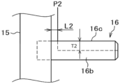
FIG. 6 is an explanatory diagram showing a wafer support state of the boat of FIG. 4;
Fig. 7 is a side view of the support of the boat in the first modification.
Fig. 8 is a side view of the boat posts and support pins in the second modification.
Fig. 9 is a side view of the boat posts and support pins in the third modification.
10 is a perspective view of a boat in a fourth modification.
Figure 11 is a cross-sectional view of the boat of Figure 10;
FIG. 12 is a schematic configuration diagram of a controller of the substrate processing apparatus of FIG. 1 and is a schematic block diagram showing a control system of the controller.
13 is a flowchart illustrating an operation of the substrate processing apparatus of FIG. 1 .
이하, 본 개시의 실시 형태에 대해서, 도 1 내지 도 13을 참조하면서 설명한다. 기판 처리 장치(10)는, 반도체 장치의 제조 공정에서 사용되는 장치의 일례로서 구성되어 있다.EMBODIMENT OF THE INVENTION Hereinafter, embodiment of this indication is described, referring FIGS. 1-13. The
(1) 기판 처리 장치의 구성(1) Configuration of substrate processing apparatus
기판 처리 장치(10)는, 가열부(가열 기구, 가열계)로서의 히터(207)가 마련된 처리로(202)를 구비한다. 히터(207)는 원통 형상이며, 보유 지지판으로서의 히터 베이스(도시하지 않음)에 지지됨으로써 수직으로 거치되어 있다.The
[아우터 튜브(외통, 외부관)(203)][Outer tube (outer tube, outer tube) (203)]
히터(207)의 내측에는, 히터(207)와 동심원형으로 반응 용기(처리 용기)를 구성하는 아우터 튜브(외통, 외부관이라고도 칭함)(203)가 배치되어 있다. 아우터 튜브(203)는, 예를 들어 석영(SiO2), 탄화실리콘(SiC) 등의 내열성 재료에 의해 구성되고, 상단이 폐색되고 하단이 개구된 원통 형상으로 형성되어 있다. 아우터 튜브(203)의 하방에는, 아우터 튜브(203)와 동심원형으로, 매니폴드(인렛 플랜지)(209)가 배치되어 있다. 매니폴드(209)는, 예를 들어 스테인리스(SUS) 등의 금속에 의해 구성되고, 상단 및 하단이 개구된 원통 형상으로 형성되어 있다. 매니폴드(209)의 상단부와, 아우터 튜브(203)의 사이에는, 시일 부재로서의 O링(220a)이 마련되어 있다. 매니폴드(209)가 히터 베이스에 지지됨으로써, 아우터 튜브(203)는 수직으로 거치된 상태가 된다.Inside the
[이너 튜브(내통, 내부관)(204)][Inner tube (inner tube, inner tube) (204)]
아우터 튜브(203)의 내측에는, 반응 용기를 구성하는 이너 튜브(내통, 내부관이라고도 칭함)(204)가 배치되어 있다. 이너 튜브(204)는, 예를 들어 석영, SiC 등의 내열성 재료에 의해 구성되고, 상단이 폐색되고 하단이 개구된 원통 형상으로 형성되어 있다. 주로, 아우터 튜브(203)와, 이너 튜브(204)와, 매니폴드(209)에 의해 처리 용기(반응 용기)가 구성되어 있다. 처리 용기의 통 중공부(이너 튜브(204)의 내측)에는 처리실(201)이 형성되어 있다.Inside the
처리실(201)은, 기판으로서의 웨이퍼(200)를 후술하는 보트(217)에 의해 수평 자세로 연직 방향으로 다단으로 배열한 상태에서 수용 가능하게 구성되어 있다. 처리실(201) 내에는, 노즐(410(제1 노즐), 420(제2 노즐))이 매니폴드(209)의 측벽 및 이너 튜브(204)를 관통하도록 마련되어 있다. 노즐(410, 420)에는, 가스 공급 라인으로서의 가스 공급관(310, 320)이 각각 접속되어 있다. 이와 같이, 기판 처리 장치(10)에는 2개의 노즐(410, 420)과, 2개의 가스 공급관(310, 320)이 마련되어 있어, 처리실(201) 내에 복수 종류의 가스를 공급할 수 있도록 구성되어 있다. 단, 본 실시 형태의 처리로(202)는 상술한 형태에 한정되지 않는다.The
[가스 공급부][Gas Supply Unit]
가스 공급관(310, 320)에는, 도 3에 도시하는 바와 같이, 상류측부터 차례로 유량 제어기(유량 제어부)인 매스 플로우 컨트롤러(MFC)(312, 322)가 각각 마련되어 있다. 또한, 가스 공급관(310, 320)에는, 개폐 밸브인 밸브(314, 324)가 각각 마련되어 있다. 가스 공급관(310, 320)의 밸브(314, 324)의 하류측에는, 불활성 가스를 공급하는 가스 공급관(510, 520)이 각각 접속되어 있다. 가스 공급관(510, 520)에는, 상류측부터 차례로 유량 제어기(유량 제어부)인 MFC(512, 522) 및 개폐 밸브인 밸브(514, 524)가 각각 마련되어 있다.As shown in FIG. 3 , the
가스 공급관(310, 320)의 선단부에는 노즐(410, 420)이 각각 연결 접속되어 있다. 노즐(410, 420)은, L자형의 노즐로서 구성되어 있고, 그 수평부는 매니폴드(209)의 측벽 및 이너 튜브(204)를 관통하도록 마련되어 있다. 노즐(410, 420)의 수직부는, 이너 튜브(204)의 직경 방향 외향으로 돌출되고 또한 연직 방향으로 연장되도록 형성되어 있는 채널 형상(홈 형상)의 예비실(201a)의 내부에 마련되어 있고, 예비실(201a) 내에서 이너 튜브(204)의 내벽을 따라 상방(웨이퍼(200)의 배열 방향 상방)을 향해서 마련되어 있다. 또한, 노즐(410, 420)은, 예비실(201a)의 개구(201b)보다도 외측에 배치된다. 또한, 도 3의 파선으로 나타내는 바와 같이, 클리닝 가스 또는 불활성 가스를 공급 가능한 가스 공급관(330, 340)에 접속되는 제3 노즐(도시하지 않음), 제4 노즐(도시하지 않음)이 마련되어도 된다.
노즐(410, 420)은, 처리실(201)의 하부 영역부터 처리실(201)의 상부 영역까지 연장되도록 마련되어 있고, 웨이퍼(200)와 대향하는 위치에 각각 복수의 가스 공급 구멍(410a, 420a)이 마련되어 있다. 이에 의해, 노즐(410, 420)의 가스 공급 구멍(개구부)(410a, 420a)으로부터 각각 웨이퍼(200)에 처리 가스를 공급한다.The
가스 공급 구멍(410a)은, 이너 튜브(204)의 하부로부터 상부에 걸쳐 복수 마련되고, 각각 동일한 개구 면적을 갖고, 또한 동일한 개구 피치로 마련되어 있다. 단, 가스 공급 구멍(410a)은 상술한 형태에 한정되지 않는다. 예를 들어, 이너 튜브(204)의 하부로부터 상부를 향해서 개구 면적을 점차 크게 해도 된다. 이에 의해, 가스 공급 구멍(410a)으로부터 공급되는 가스의 유량을 보다 균일화하는 것이 가능하게 된다.A plurality of
가스 공급 구멍(420a)은, 이너 튜브(204)의 하부로부터 상부에 걸쳐 복수 마련되고, 각각 동일한 개구 면적을 갖고, 또한 동일한 개구 피치로 마련되어 있다. 단, 가스 공급 구멍(420a)은 상술한 형태에 한정되지 않는다. 예를 들어, 이너 튜브(204)의 하부로부터 상부를 향해서 개구 면적을 점차 크게 해도 된다. 이에 의해, 가스 공급 구멍(420a)으로부터 공급되는 가스의 유량을 보다 균일화하는 것이 가능하게 된다.A plurality of
노즐(410, 420)의 가스 공급 구멍(410a, 420a)은, 후술하는 보트(217)의 하부부터 상부까지의 높이의 위치에 복수 마련되어 있다. 그 때문에, 노즐(410, 420)의 가스 공급 구멍(410a, 420a)으로부터 처리실(201) 내에 공급된 처리 가스는, 보트(217)의 하부부터 상부까지 수용된 웨이퍼(200), 즉 보트(217)에 수용된 웨이퍼(200)의 전역에 공급된다. 노즐(410, 420)은, 처리실(201)의 하부 영역부터 상부 영역까지 연장되도록 마련되어 있으면 되지만, 보트(217)의 천장 부근까지 연장되도록 마련되어 있는 것이 바람직하다.A plurality of
가스 공급관(310)으로부터는, 처리 가스로서, 제1 금속 원소를 포함하는 원료 가스(제1 금속 함유 가스, 제1 원료 가스)가, MFC(312), 밸브(314), 노즐(410)을 통해서 처리실(201) 내에 공급된다. 원료로서는, 예를 들어 금속 원소인 알루미늄(Al)을 포함하는 금속 함유 원료 가스(금속 함유 가스)인 알루미늄 함유 원료(Al 함유 원료 가스, Al 함유 가스)로서의 트리메틸알루미늄(Al(CH3)3, 약칭: TMA)이 사용된다. TMA는 유기계 원료이며, 알루미늄에 알킬기가 결합한 알킬알루미늄이다. 그 밖에 원료로서는, 금속 함유 가스이며, 유기계 원료이며, 예를 들어 지르코늄(Zr)을 포함하는 테트라키스에틸메틸아미노지르코늄(TEMAZ, Zr[N(CH3)C2H5]4)을 사용할 수 있다. TEMAZ는, 상온 상압에서 액체이며, 도시하지 않은 기화기에서 기화해서 기화 가스인 TEMAZ 가스로서 사용된다.From the
가스 공급관(320)으로부터는, 처리 가스로서, 반응 가스가, MFC(322), 밸브(324), 노즐(420)을 통해서 처리실(201) 내에 공급된다. 반응 가스로서는, 산소(O)를 포함하고, Al과 반응하는 반응 가스(리액턴트)로서의 산소 함유 가스(산화 가스, 산화제)를 사용할 수 있다. 산소 함유 가스로서는, 예를 들어 오존(O3) 가스를 사용할 수 있다. 또한, 가스 공급관(320)에, 도 3의 점선으로 나타내는, 플러쉬 탱크(321)를 마련해도 된다. 플러쉬 탱크(321)를 마련함으로써, 웨이퍼(200)에 대하여 O3 가스를 대량으로 공급시키는 것이 가능하게 된다.From the
본 실시 형태에 있어서, 금속 함유 가스인 원료 가스가 노즐(410)의 가스 공급 구멍(410a)으로부터 처리실(201) 내에 공급되고, 산소 함유 가스인 반응 가스가 노즐(420)의 가스 공급 구멍(420a)으로부터 처리실(201) 내에 공급됨으로써, 웨이퍼(200)의 표면에 원료 가스(금속 함유 가스) 및 반응 가스(산소 함유 가스)가 공급되어, 웨이퍼(200)의 표면 상에 금속 산화막이 형성된다.In the present embodiment, source gas, which is a metal-containing gas, is supplied into the
가스 공급관(510, 520)으로부터는, 불활성 가스로서, 예를 들어 질소(N2) 가스가, 각각 MFC(512, 522), 밸브(514, 524), 노즐(410, 420)을 통해서 처리실(201) 내에 공급된다. 또한, 이하, 불활성 가스로서 N2 가스를 사용하는 예에 대해서 설명하지만, 불활성 가스로서는, N2 가스 이외에, 예를 들어 아르곤(Ar) 가스, 헬륨(He) 가스, 네온(Ne) 가스, 크세논(Xe) 가스 등의 희가스를 사용해도 된다.From the
주로, 노즐(410, 420)로 가스 공급계(가스 공급부)가 구성된다. 또한, 가스 공급관(310, 320), MFC(312, 322), 밸브(314, 324), 노즐(410, 420)에 의해 처리 가스 공급계(가스 공급부)가 구성되어도 된다. 또한, 가스 공급관(310)과 가스 공급관(320)의 적어도 어느 것을 가스 공급부로서 생각해도 된다. 처리 가스 공급계를, 간단히 가스 공급계라고 칭할 수도 있다. 가스 공급관(310)으로부터 원료 가스를 흘리는 경우, 주로, 가스 공급관(310), MFC(312), 밸브(314)에 의해 원료 가스 공급계가 구성되지만, 노즐(410)을 원료 가스 공급계에 포함해서 생각해도 된다. 또한, 원료 가스 공급계를 원료 공급계라고 칭할 수도 있다. 원료 가스로서 금속 함유 원료 가스를 사용하는 경우, 원료 가스 공급계를 금속 함유 원료 가스 공급계라고 칭할 수도 있다. 가스 공급관(320)으로부터 반응 가스를 흘리는 경우, 주로, 가스 공급관(320), MFC(322), 밸브(324)에 의해 반응 가스 공급계가 구성되지만, 노즐(420)을 반응 가스 공급계에 포함해서 생각해도 된다. 가스 공급관(320)으로부터 반응 가스로서 산소 함유 가스를 공급하는 경우, 반응 가스 공급계를 산소 함유 가스 공급계라고 칭할 수도 있다. 또한, 주로, 가스 공급관(510, 520), MFC(512, 522), 밸브(514, 524)에 의해 불활성 가스 공급계가 구성된다. 불활성 가스 공급계를, 퍼지 가스 공급계, 희석 가스 공급계, 혹은 캐리어 가스 공급계라고 칭할 수도 있다.Mainly, the
본 실시 형태에서의 가스 공급의 방법은, 이너 튜브(204)의 내벽과, 복수매의 웨이퍼(200)의 단부로 정의되는 원환상의 세로로 긴 공간 내, 즉, 원통상의 공간 내의 예비실(201a) 내에 배치한 노즐(410, 420)을 경유해서 가스를 반송하고 있다. 그리고, 노즐(410, 420)의 웨이퍼와 대향하는 위치에 마련된 복수의 가스 공급 구멍(410a, 420a)으로부터 이너 튜브(204) 내에 가스를 분출시키고 있다. 보다 상세하게는, 노즐(410)의 가스 공급 구멍(410a), 노즐(420)의 가스 공급 구멍(420a)에 의해, 웨이퍼(200)의 표면과 평행 방향, 즉 수평 방향을 향해서 원료 가스 등을 분출시키고 있다.The gas supply method in the present embodiment is a preliminary chamber in an annular vertically long space defined by an inner wall of an
[배기부][Exhaust]
배기 구멍(배기구)(204a)은, 이너 튜브(204)의 측벽이며 노즐(410, 420)에 대향한 위치, 즉 예비실(201a)과는 180도 반대측의 위치에 형성된 관통 구멍이며, 예를 들어 연직 방향으로 가늘고 길게 개설된 슬릿상의 관통 구멍이다. 그 때문에, 노즐(410, 420)의 가스 공급 구멍(410a, 420a)으로부터 처리실(201) 내에 공급되어, 웨이퍼(200)의 표면 상을 흐른 가스, 즉, 잔류하는 가스(잔류 가스)는, 배기 구멍(204a)을 통해서 이너 튜브(204)와 아우터 튜브(203)의 사이에 형성된 간극에 의해 구성되는 배기로(206) 내에 흐른다. 그리고, 배기로(206) 내에 흐른 가스는, 배기관(231) 내에 흘러, 처리로(202) 밖으로 배출된다. 또한, 배기부는, 적어도 배기관(231)으로 구성된다.The exhaust hole (exhaust port) 204a is a side wall of the
배기 구멍(204a)은, 복수의 웨이퍼(200)와 대향하는 위치(바람직하게는 보트(217)의 상부로부터 하부와 대향하는 위치)에 마련되어 있고, 가스 공급 구멍(410a, 420a)으로부터 처리실(201) 내의 웨이퍼(200)의 근방에 공급된 가스는, 수평 방향, 즉 웨이퍼(200)의 표면과 평행 방향을 향해서 흐른 후, 배기 구멍(204a)을 통해서 배기로(206) 내에 흐른다. 즉, 처리실(201)에 잔류하는 가스는, 배기 구멍(204a)을 통해서 웨이퍼(200)의 주면에 대하여 평행하게 배기된다. 또한, 배기 구멍(204a)은, 슬릿상의 관통 구멍으로서 구성되는 경우에 한하지 않고, 복수개의 구멍에 의해 구성되어 있어도 된다.The
매니폴드(209)에는, 처리실(201) 내의 분위기를 배기하는 배기관(231)이 마련되어 있다. 배기관(231)에는, 상류측부터 차례로 처리실(201) 내의 압력을 검출하는 압력 검출기(압력 검출부)로서의 압력 센서(245), APC(Auto Pressure Controller) 밸브(243), 진공 배기 장치로서의 진공 펌프(246)가 접속되어 있다. APC 밸브(243)는, 진공 펌프(246)를 작동시킨 상태에서 밸브를 개폐함으로써, 처리실(201) 내의 진공 배기 및 진공 배기 정지를 행할 수 있고, 또한 진공 펌프(246)를 작동시킨 상태에서 밸브 개방도를 조절함으로써, 처리실(201) 내의 압력을 조정할 수 있다. 주로, 배기 구멍(204a), 배기로(206), 배기관(231), APC 밸브(243) 및 압력 센서(245)에 의해, 배기계, 즉 배기 라인이 구성된다. 또한, 진공 펌프(246)를 배기계에 포함해서 생각해도 된다.An
도 1에 도시하는 바와 같이, 매니폴드(209)의 하방에는, 매니폴드(209)의 하단 개구를 기밀하게 폐색 가능한 노구 덮개로서의 시일 캡(219)이 마련되어 있어도 된다. 시일 캡(219)은, 매니폴드(209)의 하단에 연직 방향 하측으로부터 맞닿아지도록 구성되어 있다. 시일 캡(219)은, 예를 들어 SUS 등의 금속에 의해 구성되고, 원반상으로 형성되어 있다. 시일 캡(219)의 상면에는, 매니폴드(209)의 하단과 맞닿는 시일 부재로서의 O링(220b)이 마련되어 있다. 시일 캡(219)에서의 처리실(201)의 반대측에는, 웨이퍼(200)를 수용하는 보트(217)를 회전시키는 회전 기구(267)가 설치되어 있다. 회전 기구(267)의 회전축(255)은, 시일 캡(219)을 관통해서 보트(217)에 접속되어 있다. 회전 기구(267)는, 보트(217)를 회전시킴으로써 웨이퍼(200)를 회전시키도록 구성되어 있다. 시일 캡(219)은, 아우터 튜브(203)의 외부에 수직으로 설치된 승강 기구로서의 보트 엘리베이터(115)에 의해 연직 방향으로 승강되도록 구성되어 있다. 보트 엘리베이터(115)는, 시일 캡(219)을 승강시킴으로써, 보트(217)를 처리실(201) 내외로 반입 및 반출하는 것이 가능하게 구성되어 있다. 보트 엘리베이터(115)는, 보트(217) 및 보트(217)에 수용된 웨이퍼(200)를 처리실(201) 내외로 반송하는 반송 장치(반송 기구)로서 구성되어 있다.As shown in FIG. 1 , below the manifold 209, a
기판 지지구로서의 보트(217)는, 복수매, 예를 들어 25 내지 200매의 웨이퍼(200)를 수평 자세이면서 또한 서로 중심을 맞춘 상태에서 연직 방향으로 정렬시켜 다단으로 지지하도록, 즉, 간격을 두고 배열시키도록 구성되어 있다. 보트(217)의 상세에 대해서는 후술한다. 보트(217)의 하부에는, 예를 들어 석영이나 SiC 등의 내열성 재료에 의해 구성되는 단열부(218)가 마련되어 있다. 이 구성에 의해, 히터(207)로부터의 열이 시일 캡(219)측에 전해지기 어렵게 되어 있다.The
도 2에 도시한 바와 같이, 이너 튜브(204) 내에는 온도 검출기로서의 온도 센서(263)가 설치되어 있고, 온도 센서(263)에 의해 검출된 온도 정보에 기초하여 히터(207)에 대한 통전량을 조정함으로써, 처리실(201) 내의 온도가 원하는 온도 분포로 되도록 구성되어 있다. 온도 센서(263)는, 노즐(410 및 420)과 마찬가지로 L자형으로 구성되어 있고, 이너 튜브(204)의 내벽을 따라 마련되어 있다.As shown in FIG. 2 , a
이와 같이 구성함으로써, 보트(217)의 적어도 웨이퍼(200)를 지지하는 영역의 온도가 균일하게 유지되도록 구성된다. 이 균열의 온도 영역(균열 영역(T1))의 온도와 T1보다도 하측의 영역의 온도에는 차가 있다. 또한, T1은, 기판 처리 영역이라고도 칭한다. 기판 처리 영역의 세로 방향 길이는, 균열 영역의 세로 방향의 길이 이하로 구성된다. 또한, 기판 처리 영역이란, 보트(217)의 세로 방향 위치 중, 웨이퍼(200)가 지지(적재)되는 위치를 의미한다. 여기서, 웨이퍼(200)란, 제품 웨이퍼나 더미 웨이퍼, 필 더미 웨이퍼의 적어도 어느 것을 의미한다. 또한, 기판 처리 영역이란, 보트(217)에 있어서, 웨이퍼(200)를 보유 지지하는 영역을 의미한다. 즉, 기판 처리 영역은, 기판 보유 지지 영역이라고도 칭한다.With this configuration, the temperature of at least the region of the
[보트(기판 지지구)(217)][Boat (substrate support) 217]
보트(217)는, 도 4에 도시한 바와 같이, 2매의 평행한 판으로서의 저판(12) 및 천장판(11)과, 저판(12)과 천장판(11)의 사이에 대략 수직으로 마련된 복수개, 예를 들어 3개의 지주(15)를 갖는다. 지주(15)는 원주상을 하고 있다. 웨이퍼(200)를 안정하면서도 또한 심플하게 지지하기 위해서는, 지주(15)의 수는 3개인 것이 바람직하지만, 3개 초과이어도 된다. 보트(217)의 적어도 지주(15)는, 예를 들어 금속 부재인 스테인리스에, 금속 산화물의 막(금속 산화막)인 크롬 산화막(CrO막)을 코팅(피복)한 것으로 구성된다. 스테인리스로서는, 예를 들어 SUS316L, SUS836L, SUS310S가 바람직하다. 스테인리스에는, 웨이퍼(200)나 웨이퍼(200) 상에 형성되는 막의 특성을 저하시키는 경우가 있는 금속 원소(예를 들어, Fe, Ni, Cr, Cu 등)가 포함되어 있다. 이들 금속 원소가 불순물로서, 웨이퍼(200)나 웨이퍼(200) 상에 형성되는 막 내에 들어가는 것을 금속 오염이라고 칭한다.As shown in FIG. 4, the
3개의 지주(15)는, 저판(12)에 대략 반원상으로 배열되어 고정되어 있다. 천장판(11)은, 3개의 지주(15)의 상단부에 고정되어 있다. 도 5에 도시한 바와 같이, 보트(217)는 복수의 지주(15)를 갖고, 지지되는 웨이퍼(200)의 외주를 따라 기준이 되는 지주(15)가 마련되고, 기준이 되는 지주(15)는 일점쇄선으로 나타낸 기준선(D) 상에 위치하고, 이 기준선(D)에 대하여 좌우 대칭이 되는 위치에 마련되도록 구성되어 있다.The three
도 4, 6에 도시하는 바와 같이, 각 지주(15)에는, 복수의 웨이퍼(200)를 수직 방향으로 소정의 간격(P)으로 배열시켜서 대략 수평 자세로 지지(적재)하는 것이 가능한 복수의 지지부(적재부)로서의 지지 핀(16)이 다단으로 마련된다. 지지 핀(16)은, 지주(15)와 동일하게 스테인리스에 의해 구성되고, 보트(217)의 내측을 향해서 돌출 설치된다. 도 5에 도시한 바와 같이, 각 지지 핀(16)은, 원주상을 하고 있고, 보트(217)의 중심, 즉 웨이퍼(200)의 중심을 향해서 돌출 설치되어 있다. 이 경우, 지주(15)에는, 각각 1개씩 지지 핀(16)을 마련한다. 즉, 1단에 3개의 지지 핀(16)이 돌출 설치되어 있다. 이 돌출 설치된 3개의 지지 핀(16) 상에 웨이퍼(200)의 외주를 지지시킴으로써, 웨이퍼(200)를 지지하도록 되어 있다. 이 지지 핀(16)은, 수평도가 유지되어 있는 것이 바람직하다. 수평을 유지함으로써, 웨이퍼(200)를 반송 중에 웨이퍼(200)가 지지 핀(16)에 접촉하는 등의 간섭을 피할 수 있고, 또한 보트(217)에 웨이퍼(200)가 지지된 상태에서의 웨이퍼 상에 균일한 가스의 흐름을 확보할 수 있다.As shown in FIGS. 4 and 6 , on each
본 실시 형태의 보트(217)의 지주(15)는 금속 부재로 구성되어 있기 때문에, 종래의 석영이나 SiC로 구성된 보트의 지주보다도 가늘게 구성될 수 있다. 예를 들어, 종래의 보트의 지주의 직경(φ)은 19mm이며, 도 6에 도시하는 본 실시 형태의 보트(217)의 지주(15)의 직경(φ)은 5 내지 10mm이다. 지주(15)의 직경은, 지지 핀(16)에 웨이퍼(200)를 지지 가능한 강도를 갖도록 미리 설정되어 있다. 따라서, 본 실시 형태에서의 지주(15)의 직경(φ)(5 내지 10mm)은 일례이며, 지주(15)의 개수에 따라 웨이퍼(200)를 지지 가능한 강도를 갖는 직경이 5mm 미만으로 되는 경우도, 본 실시 형태에 포함된다.Since the
예를 들어, 지주(15)의 직경이 작아지면, 성막 가스의 흐름을 방해하기 어려우므로 체류가 일어나기 어렵다. 또한, 지주(15)의 표면적이 작아지기 때문에, 성막 가스의 소비가 감소한다. 따라서, 각 지주(15) 부근의 막 두께의 저하에 의한 막 두께 균일성의 저하를 경감할 수 있다. 또한, 지주(15)의 직경을 작게 하는데 수반하여, 지지 핀(16)의 직경도 작게 할 필요가 있다. 그러나 본 실시 형태에 따르면, 지지 핀(16)을 지주(15)와 동일하게 금속 부재인 스테인리스로 구성함으로써, 웨이퍼(200)를 지지 가능한 강도를 확보할 수 있다.For example, when the diameter of the
지지 핀(16)은 지주(15)에 마련된 구멍에 삽입되어, 용접 등에 의해 소정의 간격(P)(예를 들어 8mm 피치)으로 고정되어 있다. 또한, 도 6에 도시하는 바와 같이, 원주상으로 한 지지 핀(16)의 선단(16a)은, 둥글게 하거나, 혹은 모따기를 행하면 된다.The support pins 16 are inserted into holes provided in the
또한, 지지 핀(16)의 적어도 웨이퍼(200)와의 접촉 개소(접촉부)는, 금속 산화막인 CrO막으로 코팅되어 있다. 지지 핀(16)의 적어도 웨이퍼(200)와의 접촉 개소를, CrO막이 아니라, 금속 원소를 포함하지 않는 비금속물의 막(비금속막)인 실리콘 산화막(SiO막)으로 코팅해도 된다.In addition, at least a contact point (contact portion) of the
또한, 지지 핀(16)의 일부 또는 전체를 CrO막으로 코팅하고, 지지 핀(16)에서의 적어도 웨이퍼(200)와의 접촉 개소를, 또한 SiO막으로 코팅해도 된다. SiO막으로 코팅되는 부분으로서는, 적어도 웨이퍼(200)와의 접촉 개소에 실시하면 되며, 더욱 바람직하게는, 지주(15)로부터 돌출된 부분 전체에 실시된다. 이에 의해, CrO막에 의한 코팅에서는, 금속 오염을 충분히 억제할 수 없는 경우에도, 웨이퍼(200)에 접촉하는 개소를 SiO막으로 코팅함으로써 금속 오염을 보다 확실하게 억제하는 것이 가능하다.Alternatively, part or all of the support pins 16 may be coated with a CrO film, and at least a contact portion of the support pins 16 with the
지지 핀(16)(지지부)은 원주상 이외에, 웨이퍼(200)와의 접촉면측에 평면을 갖는 반원주상이나 사각주상, 삼각주상 등의 다른 주상이어도 되고, 또한 판 형상이어도 된다. 또한, 웨이퍼(200)와의 접촉면측에 곡면을 갖는 반원주상이어도 된다.The support pin 16 (support part) may be a columnar shape other than a columnar shape, such as a semicircular columnar shape having a flat surface on the side of the contact surface with the
또한, 본 실시 형태에서는, 지주(15)나 지지 핀(16)을 코팅하는 금속 산화막의 적합한 예의 하나로서 CrO막을 적용했지만, 이에 한정하지 않고, 다른 적합한 금속 산화물의 막의 예의 하나로서 산화알루미늄(AlO)의 막을 적용해도 된다. 또한, 또 다른 금속 산화물의 막으로서, 산화티타늄(TiO), 산화지르코늄(ZrO), 산화하프늄(HfO) 등의 막을 적용할 수도 있다. 또한, 본 실시 형태에서는, 지주(15)나 지지 핀(16)을 금속 산화막인 CrO막으로 코팅하는 예를 설명했지만, 금속 산화막 대신에, 실리콘(Si), 산화실리콘(SiO), 질화실리콘(SiN), SiC 등의 금속 원소를 포함하지 않는 비금속물의 막에 의해 코팅해도 된다. 또한, Si로 코팅하는 방법으로서, 접촉 개소(접촉부)에 대한 부분적인 코팅이 용이한 Si 용사를 사용해도 된다.In this embodiment, a CrO film is applied as one of the suitable examples of a metal oxide film for coating the support pins 15 and 16, but the film is not limited to this, and aluminum oxide (AlO ) may be applied. Further, as a film of another metal oxide, a film of titanium oxide (TiO), zirconium oxide (ZrO), hafnium oxide (HfO), or the like can be applied. In this embodiment, an example of coating the support pins 15 and the support pins 16 with a CrO film, which is a metal oxide film, has been described, but instead of a metal oxide film, silicon (Si), silicon oxide (SiO), or silicon nitride ( You may coat with a non-metallic film which does not contain metal elements, such as SiN) and SiC. In addition, as a method of coating with Si, you may use Si spraying which facilitates partial coating of the contact area (contact part).
또한, 보트(217)를 웨이퍼(200) 상에 금속 함유막을 형성하는 처리에서 사용하는 경우, 당해 금속 함유막에 포함되는 금속에 의해 코팅을 행해도 된다. 예를 들어, 금속 함유막으로서 AlO막을 형성하는 처리에서 보트(217)를 사용하는 경우, AlO막에 포함되는 금속인 알루미늄(Al)을 용사함으로써, Al로 상술한 코팅을 행해도 된다.Further, when the
본 실시 형태에서는, 금속인 스테인리스로 지주(15)를 형성한다. 이에 의해, 석영 등의 보트의 지주와 동등한 강도를 확보하면서, 보트의 지주의 직경을 가늘게 하는 것이 가능하게 되어, 보트의 지주의 근방에서 발생하는 막 두께 저하를 억제할 수 있다.In this embodiment, the
또한, 본 실시 형태에서는, 보트(217)를 구성하는 지주(15)와 지지 핀(16)의 적어도 일부를 금속 산화막 또는 비금속막의 적어도 한쪽으로 코팅한다. 이에 의해, 보트(217)를 구성하는 금속 부재에 기인하는 웨이퍼(200)에서의 금속 오염을 억제할 수 있다.In this embodiment, at least a part of the support pins 16 and the support posts 15 constituting the
또한, 본 실시 형태에서는, 지지 핀(16)의 적어도 웨이퍼(200)와의 접촉 개소(접촉부)를, 금속 산화막 또는 비금속막의 적어도 한쪽으로 코팅한다. 이에 의해, 특히 웨이퍼(200)에 접촉하는 지지 핀(16)에 기인하는 웨이퍼(200)에서의 금속 오염을 억제할 수 있다.Further, in the present embodiment, at least a contact point (contact portion) of the
또한, 본 실시 형태에서는, 지주(15)를 금속 산화막 또는 비금속막의 적어도 한쪽으로 코팅한다. 이에 의해, 지주(15)를 구성하는 금속에 기인하는 금속 오염을 억제하여, 금속 오염의 레벨을 더욱 낮게 유지할 수 있다.In this embodiment, the
또한, 본 실시 형태와 같이, 지주(15)나 지지 핀(16)의 웨이퍼(200)와의 접촉 개소 이외의 부분을 금속 산화막 또는 비금속막의 적어도 한쪽으로 코팅함으로써, 지주(15) 등의 표면에 퇴적물의 막이 형성되었을 때, 온도 변화에 따라 지주(15) 등의 표면과 퇴적물의 막의 사이에 생기는 응력을 완화하여, 퇴적물의 막에서의 크랙이나 막 박리, 거기에 기인하는 파티클의 발생을 억제할 수도 있다. 즉, 웨이퍼(200)에 대하여 성막 처리를 행하는 경우, 성막 처리에 있어서 지주(15) 등의 표면에 형성되는 퇴적물의 막과 동일한 방향의 응력을 갖는 금속 산화막, 또는 비금속막을 응력 완충막으로서 지주(15) 등의 표면에 코팅한다. 이 경우, 코팅에 사용하는 금속 산화막이나 비금속막은, 성막 처리에서 형성되는 막종에 따라서 선택된다.In addition, as in the present embodiment, by coating at least one of a metal oxide film or a non-metal film at a portion other than the contact portion of the
또한, 본 실시 형태에서는, 스테인리스에 의해 구성된 지주(15)와 지지 핀(16) 양쪽에 대하여 금속 산화막 또는 비금속막의 적어도 한쪽으로 코팅한다. 이에 의해, 보트(217)에 대하여 한번의 처리로 코팅을 실시할 수 있다. 스테인리스의 표면에의 CrO막의 형성은, 예를 들어 스테인리스에 대한 부동태화 처리에 의해 행할 수 있다. 또한, CrO막 대신에, 웨이퍼(200)에 대한 성막 처리에서 형성되는 막과 동일한 막종(예를 들어 AlO막 등)으로 코팅을 행하는 경우, 웨이퍼(200)가 탑재되어 있지 않은 상태의 보트(217)를 처리실(201) 내에 반입하여, 웨이퍼(200)에 대한 성막 처리와 마찬가지의 처리를 행함으로써, 코팅을 행해도 된다.In this embodiment, both the
또한, 본 실시 형태에서는, 지주(15)의 표면이 CrO막 등에 의해 코팅되어 있다. 그러나, 지주(15)의 표면을 금속 산화막이나 비금속막에 의해 코팅하지 않고, 그 금속 모재가 표면에 노출된 채로 두어도 된다.In this embodiment, the surface of the
개시자에 의한 검증에 의하면, 250℃ 이상, 400℃ 이하의 조건 하에서, 적어도 8mm이상, 바람직하게는 12mm 이상, 스테인리스로 구성되는 부재와 Si 웨이퍼의 간격을 확보함으로써, 스테인리스에 기인하는 Si 웨이퍼의 금속 오염을 억제할 수 있는 것이 확인되었다. 따라서, 지주(15)의 표면으로부터 소정 거리만큼 이격되도록 웨이퍼(200)를 지지 핀(16) 상에 적재함으로써, 지주(15)의 표면을 금속 산화막이나 비금속막으로 코팅하지 않고, 지지 핀(16)의 표면을 금속 산화막과 비금속막의 적어도 한쪽으로 구성함으로써, 지주(15)나 지지 핀(16)을 구성하는 금속에 기인하는 웨이퍼(200) 등에 대한 금속 오염을 억제할 수 있다. 또한, 당해 소정 거리는, 예를 들어 400℃ 이하의 조건 하에서 보트(217)가 사용되는 경우, 8mm 이상, 보다 바람직하게는 12mm 이상으로 하는 것이 바람직하다. 이와 같이, 지주(15)의 표면에 대하여 코팅 처리를 행하지 않음으로써, 코팅 처리를 행하는 경우에 비해서, 보트(217)의 제작을 용이하게 할 수 있다.According to verification by the initiator, by securing a distance of at least 8 mm or more, preferably 12 mm or more, between the member made of stainless steel and the Si wafer under the conditions of 250 ° C. or more and 400 ° C. or less, the Si wafer caused by stainless steel It was confirmed that metal contamination can be suppressed. Therefore, by placing the
(제1 변형예)(First modified example)
도 7에 도시하는 바와 같이, 지지 핀(16) 대신에 지주(15)에 새겨 형성된 복수의 홈(15a)을 지지부(적재부)로 하여, 홈(15a)의 저면(15b) 상에 웨이퍼(200)를 지지(적재)해도 된다. 본 실시 형태의 제1 변형예에서의 지주(15)는, 실시 형태와 마찬가지로, 금속 산화막인 CrO막으로 코팅되어 있다. 특히, 홈(15a)의 반원상의 저면(15b) 중 적어도 웨이퍼(200)가 지지되는 부분(즉, 접촉 개소(접촉부))은, CrO막으로 코팅하도록 구성되어 있다.As shown in FIG. 7 , a wafer ( 200) may be supported (loaded). Like the embodiment, the
또한, 홈(15a)의 반원상의 저면(15b) 중 적어도 웨이퍼(200)와의 접촉 개소를 CrO막 대신에, 비금속막인 SiO막으로 코팅하도록 구성해도 된다.Further, at least a contact portion with the
또한, 홈부(15a)에 CrO막이 코팅되고, 홈(15a)의 반원상의 저면(15b) 중 적어도 웨이퍼(200)와의 접촉 개소를, SiO막으로 또한 코팅해도 된다.Further, the
(제2 변형예)(Second modified example)
도 8에 도시하는 바와 같이, 본 실시 형태의 제2 변형예에서의 지지 핀(16)은, 금속 부재로 구성되는 금속부(16b)와 금속 원소를 포함하지 않는 비금속 부재로 구성되는 석영부(16c)의 하이브리드 구성이다. 금속부(16b)는, 실시 형태에서의 지지 핀(16)과 마찬가지의 구조이며, 지주(15)의 구멍에 삽입해서 용접으로 고정되어 있다. 석영부(석영 부위)(16c)에는 웨이퍼(200)가 탑재된다. 석영부(16c)는, 석영의 피스에 의해 구성되고, 상술한 실시 형태에서의 원주상의 지지 핀(16) 중, 지지 핀(16)에 적재되는 웨이퍼(200)에 대향하는 상반부이며, 지주(15)로부터 용접의 영향이 없는 소정 거리(L2)의 위치(P2)로부터 지지 핀(16)의 선단까지의 범위를, 석영(SiO)으로 구성하는 것이다. 즉, 제2 변형예에서는, 적어도 웨이퍼(200)와 지지 핀(16)의 접촉 개소가 비금속인 석영부(16c)에 의해 구성되어 있다. 석영부(16c)는, 석영 대신에, 다른 비금속인 SiC나 SiN 등으로 구성되어 있어도 된다.As shown in FIG. 8 , the
금속부(16b)는, 지주(15)의 구멍에 매설되는 부분 및 지주(15)의 표면으로부터 위치(P2)까지의 부분은 단면이 원 형상이며, 위치(P2)로부터 지주(15)의 선단까지의 단면은 반원 형상이다. 석영부(16c)는, 단면이 반원 형상인 반원주 형상이다. 단, 석영부(16c)는, 반원주 형상에 한정되지 않고, 다른 주상이어도 되고, 웨이퍼(200)와의 접촉면이 평평한 판상 형상이나 칩상 형상이어도 되고, 또한 다른 형상이어도 된다. 본 개시에서는, 이들 형상을 갖는 부재를 피스상 부재라고 총칭한다. 석영부(16c)의 연직 방향의 두께(T2)는, 예를 들어 0.5mm 이상 10mm 미만, 보다 바람직하게는 1mm 이상 5mm 미만이다. 두께(T2)가 0.5mm 미만인 경우, 웨이퍼(200)를 적재함으로써 석영부(16c)가 파손될 가능성이 있다. 두께(T2)를 1mm 이상으로 함으로써, 웨이퍼(200)를 적재했을 때 석영부(16c)가 파손되는 것을 보다 확실하게 방지할 수 있다.The
금속부(16b)는, 석영부(16c)의 하방 부분 및 지주(15)의 표면으로부터 위치(P2)까지의 부분이 CrO막 및 SiO막의 적어도 어느 것에 의해 코팅되어 있다.In the
지주(15)를 구성하는 금속 부재와 지지 핀(16)의 금속부(16b)를 구성하는 금속 부재는 용접에 의해 접합된다. 용접 후, CrO막을 코팅, 또는 부동태화하는 처리를 행함으로써, 용접 개소의 용접흔이 없어져, 표면 상태는 미 용접 개소와 동일한 CrO막의 표면으로 되고, 크롬(Cr), 산소(O) 이외의 불순물 농도도, 미 용접 개소와 동등하게 할 수 있다. 또한, 웨이퍼(200)와의 접촉면은 비금속 부재인 석영부(16c)로 구성되어 있으므로, 웨이퍼(200)와의 접촉에 의해 CrO막이나 SiO막 등의 표면 코트 막이 박리되지 않는다.The metal member constituting the
또한, 제2 변형예에서는, 지주(15) 및 금속부(16b)의 표면이 CrO막 등에 의해 코팅되어 있는 형태를 설명하였다. 그러나, 제2 변형예의 또 다른 변형예로서, 지주(15) 및 금속부(16b)의 적어도 어느 것의 표면을, 금속 산화막이나 비금속막의 어느 것으로도 코팅하지 않고, 이들 금속 모재가 표면에 노출된 채로 두어도 된다. 적어도 웨이퍼(200)와 지지 핀(16)의 접촉 개소를 비금속인 석영부(16c)로 구성함으로써, 지주(15)나 금속부(16b)를 구성하는 금속에 기인하는 웨이퍼(200) 등에 대한 금속 오염을 억제할 수 있다. 이와 같이, 지주(15) 및 금속부(16b)의 적어도 어느 것의 표면에 대하여 코팅 처리를 행하지 않음으로써, 당해 코팅 처리를 행하는 경우에 비해서, 보트(217)의 제작을 용이하게 할 수 있다.In addition, in the second modified example, the form in which the surfaces of the
또한, 제2 변형예의 또 다른 변형예로서, 지지 핀(16)을 CrO막 등의 금속 산화막이나 비금속막으로 코팅함과 함께, 지지 핀(16)에서의 웨이퍼(200)와의 접촉 개소의 일부를, 석영 코트나 석영 칩 등의 석영으로 구성해도 된다. 즉, 지지 핀(16)에서의 웨이퍼(200)와의 접촉 개소는 CrO막과 석영으로 구성되도록 해도 된다.In addition, as another modification of the second modification, the
(제3 변형예)(3rd modified example)
본 실시 형태의 제3 변형예에서의 지지 핀(16)은, 전체가 석영, SiC, SiN, AlO 등의 비금속물 또는 금속 산화물로 구성되어 있다. 도 9에 도시하는 바와 같이, 지지 핀(16)은, 지지 핀(16)에 새겨 형성된 오목부로서의 나사 구멍에, 지주(15)에 마련된 구멍을 통과시킨 주상 부재로서의 나사(16d)를 삽입하여, 나사 결합함으로써 지주(15)에 고정된다. 보트(217)를 구성하는 다른 부재는, 스테인리스에 금속 산화막인 CrO막이나 비금속막인 SiO막 등이 코팅되어 있다. 지지 핀(16)에 새겨 형성된 오목부를 나사 홈이 없는 구멍으로 형성하여, 나사(16d) 대신에 나사 홈이 없는 핀 형상의 고정 부재를 오목부에 삽입함으로써 지지 핀(16)을 지주(15)에 고정해도 된다. 또한, 와이어 가공 기술을 사용해서 나사(16d)를 숨기고 플랫면을 형성하여, SiO막의 피복률을 향상시키고 있다.The
또한, 지지 핀(16)의 지주(15)측에 볼록부를 마련하여, 지주(15)에 형성된 오목부 또는 관통 구멍에 삽입하는 구조(끼워 맞추는 구조)로 구성해도 된다. 지지 핀(16)과 지주(15)의 접합은, 용접이어도 되고, 지지 핀(16)의 볼록부를 나사 형상으로 구성하고, 지주(15)의 오목부 또는 관통 구멍을 나사 구멍 형상으로 구성하여, 끼워 맞추어도 된다.Further, a convex portion may be provided on the
또한, 제3 변형예에서는, 제2 변형예의 또 다른 변형예와 마찬가지로, 지주(15)의 표면을 금속 산화막이나 비금속막에 의해 코팅하지 않고, 그 금속 모재가 표면에 노출된 채로 두어도 된다. 본 실시 형태와 같이, 웨이퍼(200)와 접촉하는 지지 핀(16)을 비금속물 또는 금속 산화물로 구성함으로써, 지주(15)를 구성하는 금속에 기인하는 웨이퍼(200) 등에 대한 금속 오염을 억제할 수 있다. 이와 같이, 지주(15)의 표면에 대하여 코팅 처리를 행하지 않음으로써, 당해 코팅 처리를 행하는 경우에 비해서, 보트(217)의 제작을 용이하게 할 수 있다.In the third modification, as in the other modification of the second modification, the surface of the
(제4 변형예)(Fourth modified example)
도 10에 도시하는 바와 같이, 본 실시 형태의 제4 변형예에서의 보트(217)는, 천장판(11)과 저판(12) 각각의 외주에 마련되어, 웨이퍼(200)를 보유 지지하는 지주(15)와, 천장판(11)과 저판(12) 각각의 외주에 마련되고, 지주(15)보다도 직경이 작은 보조 지주(18)를 구비한 구성이다. 또한, 지주(15)에는, 실시 형태 또는 제2 변형예 또는 제3 변형예와 마찬가지로, 웨이퍼(200)를 지지(적재)하는 지지부(적재부)로서의 지지 핀(16)이 마련되어 있다.As shown in FIG. 10 , the
또한, 도 11에 도시한 바와 같이, 보조 지주(18)는, 지주(15)간을 균등하게 나누는 위치에 마련된다. 구체적으로는, 보트(217)는, 지주(15)와 보조 지주(18)의 사이, 또는 보조 지주(18)의 사이를 둘레 방향으로 등간격이 되도록 구성되어 있다. 또한, 도 11에 도시한 바와 같이, 보트(217)는, 복수의 지주(15)를 갖고, 웨이퍼(200)가 지지되는 방향으로 기준이 되는 지주(15)가 마련되고, 기준이 되는 지주(15)는, 일점쇄선의 기준선(D) 상에 위치하고, 지주(15) 및 보조 지주(18)는, 이 기준선(D)에 대하여 좌우 대칭이 되는 위치에 마련된다.Further, as shown in FIG. 11 , the
또한, 보조 지주(18)의 직경은, 지주(15)의 직경보다 작고, 지지 핀(16)을 갖지 않도록 구성되어 있다. 이것은, 보조 지주(18)는, 보조적인 지주이기 때문이다. 그 개수도 4개가 아니어도 된다. 본 실시 형태에서는, 3개의 지주(15)와 4개의 보조 지주(18)가, 지주(15)와 보조 지주(18)의 사이, 또는 보조 지주(18)간에서 웨이퍼(200)의 원주 방향으로 균등하게 마련되지만, 이 형태에 한정되는 것은 아니다.In addition, the diameter of the
본 변형예의 보트(217)의 지주(15)가 실시 형태의 보트(217)의 지주(15)보다도 가늘게 구성되고, 강도 확보의 목적으로 보조 지주(18)가 4개 설치되어 있다. 예를 들어, 도 5에 도시하는 실시 형태의 보트(217)의 지주(15)의 직경(φ)은 8mm이며, 도 11에 도시하는 본 변형예의 보트(217)의 지주(15)의 직경은 φ5mm, 보조 지주(18)의 직경은 φ4mm이다.The
계속해서, 상술한 기판 처리 장치(10)의 동작을 제어하는 제어부(제어 수단)인 컨트롤러(121)의 구성에 대해서, 도 12를 사용해서 설명한다.Subsequently, the configuration of the
도 12에 도시하는 바와 같이, 제어부(제어 수단)인 컨트롤러(121)는, CPU(Central Processing Unit)(121a), RAM(Random Access Memory)(121b), 기억 장치(121c), I/O 포트(121d)를 구비한 컴퓨터로서 구성되어 있다. RAM(121b), 기억 장치(121c), I/O 포트(121d)는 내부 버스를 통해서, CPU(121a)와 데이터 교환 가능하게 구성되어 있다. 컨트롤러(121)에는, 예를 들어 터치 패널 등으로서 구성된 입출력 장치(122)가 접속되어 있다.As shown in Fig. 12, the
기억 장치(121c)는, 예를 들어 플래시 메모리, HDD(Hard Disk Drive), SSD(Solid State Drive) 등으로 구성되어 있다. 기억 장치(121c) 내에는, 기판 처리 장치의 동작을 제어하는 제어 프로그램, 후술하는 반도체 장치의 제조 방법의 수순이나 조건 등이 기재된 프로세스 레시피 등이, 판독 가능하게 저장되어 있다. 프로세스 레시피는, 후술하는 반도체 장치의 제조 방법에서의 각 공정(각 스텝, 각 수순, 각 처리)을 컨트롤러(121)에 실행시켜, 소정의 결과를 얻을 수 있게 조합된 것이며, 프로그램으로서 기능한다. 이하, 이 프로세스 레시피, 제어 프로그램 등을 총칭하여, 간단히 프로그램이라고도 한다. 본 개시에서 프로그램이라는 말을 사용한 경우에는, 프로세스 레시피 단체만을 포함하는 경우, 제어 프로그램 단체만을 포함하는 경우, 또는 프로세스 레시피 및 제어 프로그램의 조합을 포함하는 경우가 있다. RAM(121b)은, CPU(121a)에 의해 판독된 프로그램이나 데이터 등이 일시적으로 보유되는 메모리 영역(워크 에어리어)으로서 구성되어 있다.The
I/O 포트(121d)는, 상술한 MFC(312, 322, 332, 342, 352, 512, 522), 밸브(314, 324, 334, 344, 354, 514, 524), 압력 센서(245), APC 밸브(243), 진공 펌프(246), 히터(207), 온도 센서(263), 회전 기구(267), 보트 엘리베이터(115) 등에 접속되어 있다.The I/
CPU(121a)는, 기억 장치(121c)로부터 제어 프로그램을 판독해서 실행함과 함께, 입출력 장치(122)로부터의 조작 커맨드의 입력 등에 따라서 기억 장치(121c)로부터 프로세스 레시피 등을 판독하도록 구성되어 있다. CPU(121a)는, 판독한 프로세스 레시피의 내용을 따르도록, MFC(312, 322, 332, 342, 352, 512, 522)에 의한 각종 가스의 유량 조정 동작, 밸브(314, 324, 334, 344, 354, 514, 524)의 개폐 동작, APC 밸브(243)의 개폐 동작 및 APC 밸브(243)에 의한 압력 센서(245)에 기초하는 압력 조정 동작, 온도 센서(263)에 기초하는 히터(207)의 온도 조정 동작, 진공 펌프(246)의 기동 및 정지, 회전 기구(267)에 의한 보트(217)의 회전 및 회전 속도 조절 동작, 보트 엘리베이터(115)에 의한 보트(217)의 승강 동작, 보트(217)에의 웨이퍼(200)의 수용 동작 등을 제어하도록 구성되어 있다.The
컨트롤러(121)는, 외부 기억 장치(예를 들어, 자기 테이프, 플렉시블 디스크나 하드 디스크 등의 자기 디스크, CD나 DVD 등의 광 디스크, MO 등의 광자기 디스크, USB 메모리나 메모리 카드 등의 반도체 메모리)(123)에 저장된 상술한 프로그램을, 컴퓨터에 인스톨함으로써 구성할 수 있다. 기억 장치(121c)나 외부 기억 장치(123)는, 컴퓨터 판독 가능한 기록 매체로서 구성되어 있다. 이하, 이들을 총칭하여, 간단히 기록 매체라고도 한다. 본 개시에서 기록 매체는, 기억 장치(121c) 단체만을 포함하는 경우, 외부 기억 장치(123) 단체만을 포함하는 경우, 또는 그 양쪽을 포함하는 경우가 있다. 또한, 컴퓨터에의 프로그램의 제공은, 외부 기억 장치(123)를 사용하지 않고, 인터넷이나 전용 회선 등의 통신 수단을 사용해서 행해도 된다.The
(2) 기판 처리 공정(반도체 디바이스의 제조 공정)(2) Substrate treatment process (semiconductor device manufacturing process)
반도체 장치(디바이스)의 제조 공정의 일 공정으로서, 웨이퍼(200) 상에 막을 형성하는 공정의 일례에 대해서, 도 13을 사용해서 설명한다. 이하의 설명에서, 기판 처리 장치(10)를 구성하는 각 부의 동작은 컨트롤러(121)에 의해 제어된다.An example of a process of forming a film on the
이하의 제1 예에서는, 기판으로서의 웨이퍼(200)가 적재된 상태에서 수용된 처리실(201)을 소정 온도에서 가열하면서, 처리실(201)에, 노즐(410)에 개구되는 복수의 가스 공급 구멍(410a)으로부터 원료 가스로서 TMA 가스를 공급하는 공정과, 노즐(420)에 개구되는 복수의 가스 공급 구멍(420a)으로부터 반응 가스로서 O3 가스를 공급하는 공정을 각각 소정 횟수 행하여, 웨이퍼(200) 상에 금속 산화막으로서의 AlO막을 형성한다.In the following first example, while heating the
본 개시에서 「웨이퍼」라는 말을 사용한 경우에는, 웨이퍼 그 자체를 의미하는 경우나, 웨이퍼와 그 표면에 형성된 소정의 층이나 막의 적층체를 의미하는 경우가 있다. 본 개시에서 「웨이퍼의 표면」이라는 말을 사용한 경우에는, 웨이퍼 그 자체의 표면을 의미하는 경우나, 웨이퍼 상에 형성된 소정의 층 등의 표면을 의미하는 경우가 있다. 본 개시에서 「웨이퍼 상에 소정의 층을 형성한다」라고 기재한 경우에는, 웨이퍼 그 자체의 표면 상에 소정의 층을 직접 형성하는 것을 의미하는 경우나, 웨이퍼 상에 형성되어 있는 층 등의 위에 소정의 층을 형성하는 것을 의미하는 경우가 있다. 본 개시에서 「기판」이라는 말을 사용한 경우도, 「웨이퍼」라는 말을 사용한 경우와 동의이다.When the word "wafer" is used in the present disclosure, it may mean the wafer itself or a laminate of a wafer and a predetermined layer or film formed on its surface. When the term "surface of a wafer" is used in the present disclosure, it may mean the surface of the wafer itself or the surface of a predetermined layer formed on the wafer. In the present disclosure, in the case of "forming a predetermined layer on a wafer", it means directly forming a predetermined layer on the surface of the wafer itself, or on a layer or the like formed on the wafer. In some cases, it means forming a predetermined layer. In the present disclosure, the use of the term "substrate" is synonymous with the use of the term "wafer".
이하에, 성막 공정 S300을 포함하는 기판 처리 공정에 대해서, 도 1, 도 13을 사용해서 설명한다.Below, the substrate processing process including film-forming process S300 is demonstrated using FIG.1, FIG.13.
(기판 반입 공정 S301)(substrate loading process S301)
복수매의 웨이퍼(200)가 보트(217)의 지지 핀(16) 상에 각각 장전(웨이퍼 차지)되면, 도 1에 도시한 바와 같이, 복수매의 웨이퍼(200)가 수용된 보트(217)는, 보트 엘리베이터(115)에 의해 들어 올려져서 처리실(201) 내에 반입(보트 로드)된다. 이 상태에서, 시일 캡(219)은, O링(220b)을 통해서 매니폴드(209)의 하단을 시일한 상태가 된다.When a plurality of
(분위기 조정 공정 S302)(atmosphere adjustment process S302)
계속해서, 처리실(201) 내, 즉, 웨이퍼(200)가 존재하는 공간이 원하는 압력(진공도)으로 되도록 진공 펌프(246)에 의해 진공 배기된다. 이때, 처리실(201) 내의 압력은, 압력 센서(245)로 측정되고, 이 측정된 압력 정보에 기초하여, APC 밸브(243)가 피드백 제어된다(압력 조정). 진공 펌프(246)는, 적어도 웨이퍼(200)에 대한 처리가 완료될 때까지의 동안은 상시 작동시킨 상태를 유지한다. 또한, 처리실(201) 내가 원하는 온도로 되도록 히터(207)에 의해 가열된다. 이때, 처리실(201) 내가 원하는 온도 분포로 되도록, 온도 센서(263)가 검출한 온도 정보에 기초하여 히터(207)에 대한 통전량이 피드백 제어된다(온도 조정). 히터(207)에 의한 처리실(201) 내의 가열은, 적어도 웨이퍼(200)에 대한 처리가 완료될 때까지의 동안은 계속해서 행하여진다. 또한, 보트(217)를 회전시키는 경우에는, 회전 기구(267)에 의해 보트(217) 및 웨이퍼(200)의 회전을 개시한다. 회전 기구(267)에 의한 보트(217) 및 웨이퍼(200)의 회전은, 적어도, 웨이퍼(200)에 대한 처리가 완료될 때까지의 동안은 계속해서 행하여진다. 또한, 단열부(218)의 하부에 불활성 가스로서 N2 가스를 가스 공급관(350)으로부터 공급을 개시해도 된다. 구체적으로는, 밸브(354)를 개방하여, MFC(352)로, N2 가스 유량을 0.1 내지 2slm의 범위의 유량으로 조정한다. MFC(352)의 유량은, 바람직하게는 0.3slm 내지 0.5slm으로 한다.Subsequently, the
[성막 공정 S300][Film Formation Step S300]
계속해서, 제1 공정(원료 가스 공급 공정), 퍼지 공정(잔류 가스 제거 공정), 제2 공정(반응 가스 공급 공정), 퍼지 공정(잔류 가스 제거 공정)을 이 순으로 소정 횟수(N)(N≥1) 행하여, AlO막을 형성한다.Subsequently, the first process (source gas supply process), the purge process (residual gas removal process), the second process (reaction gas supply process), and the purge process (residual gas removal process) are performed in this order a predetermined number of times (N) ( N≥1) to form an AlO film.
(제1 공정 S303(제1 가스 공급))(First step S303 (first gas supply))
밸브(314)를 개방하여, 가스 공급관(310) 내에 제1 가스(원료 가스)인 TMA 가스를 흘린다. TMA 가스는, MFC(312)에 의해 유량 조정되어, 노즐(410)의 가스 공급 구멍(410a)으로부터 처리실(201) 내에 공급되어, 배기관(231)으로부터 배기된다. 이때, 웨이퍼(200)에 대하여 TMA 가스가 공급되게 된다. 이때 동시에 밸브(514)를 개방하여, 가스 공급관(510) 내에 N2 가스 등의 불활성 가스를 흘려도 된다. 가스 공급관(510) 내를 흐른 N2 가스는, MFC(512)에 의해 유량 조정되어, TMA 가스와 함께 처리실(201) 내에 공급되어, 배기관(231)으로부터 배기된다. N2 가스는, 가스 공급관(320), 노즐(420)을 통해서 처리실(201) 내에 공급되어, 배기관(231)으로부터 배기된다.The
이때, APC 밸브(243)를 조정하여, 처리실(201) 내의 압력을, 예를 들어 1 내지 1000Pa, 바람직하게는 1 내지 100Pa, 보다 바람직하게는 10 내지 50Pa의 범위 내의 압력으로 한다. 처리실(201) 내의 압력을 1000Pa 이하로 함으로써, 후술하는 잔류 가스 제거를 적합하게 행할 수 있음과 함께, 노즐(410) 내에서 TMA 가스가 자기 분해해서 노즐(410)의 내벽에 퇴적되어버리는 것을 억제할 수 있다. 처리실(201) 내의 압력을 1Pa 이상으로 함으로써, 웨이퍼(200) 표면에서의 TMA 가스의 반응 속도를 높일 수 있어, 실용적인 성막 속도를 얻는 것이 가능하게 된다. 또한, 본 개시에서는, 수치의 범위로서, 예를 들어 1 내지 1000Pa로 기재한 경우에는, 1Pa 이상 1000Pa 이하를 의미한다. 즉, 수치의 범위 내에는 1Pa 및 1000Pa이 포함된다. 압력뿐만 아니라, 유량, 시간, 온도 등, 본 개시에 기재되는 모든 수치에 대해서 마찬가지이다.At this time, the
MFC(312)로 제어하는 TMA 가스의 공급 유량은, 예를 들어 10 내지 2000sccm, 바람직하게는 50 내지 1000sccm, 보다 바람직하게는 100 내지 500sccm의 범위 내의 유량으로 한다. 유량을 2000sccm 이하로 함으로써, 후술하는 잔류 가스 제거를 적합하게 행할 수 있음과 함께, 노즐(410) 내에서 TMA 가스가 자기 분해해서 노즐(410)의 내벽에 퇴적되어버리는 것을 억제할 수 있다. 유량을 10sccm 이상으로 함으로써, 웨이퍼(200) 표면에서의 TMA 가스의 반응 속도를 높일 수 있어, 실용적인 성막 속도를 얻는 것이 가능하게 된다.The supply flow rate of the TMA gas controlled by the
MFC(512)로 제어하는 N2 가스의 공급 유량은, 예를 들어 1 내지 30slm, 바람직하게는 1 내지 20slm, 보다 바람직하게는 1 내지 10slm의 범위 내의 유량으로 한다.The supply flow rate of the N 2 gas controlled by the
TMA 가스를 웨이퍼(200)에 대하여 공급하는 시간은, 예를 들어 1 내지 60초, 바람직하게 1 내지 20초, 보다 바람직하게는 2 내지 15초의 범위 내로 한다.The supply time of the TMA gas to the
히터(207)는, 웨이퍼(200)의 온도가, 예를 들어 실온 내지 400℃, 바람직하게는 90 내지 400℃, 보다 바람직하게는 150 내지 400℃의 범위 내가 되도록 가열한다. 온도를 400℃ 이하로 한다. 온도의 하한은, 반응 가스로서 사용되는 산화제의 특성에 따라 변화시키는 것이 가능하게 된다. 또한, 온도의 상한을 400℃로 함으로써, 상술한 실시 형태나 그 변형예에서 개시한 보트(217)를 사용해서 당해 기판 처리 공정을 행했을 때, 웨이퍼(200)에 대한 금속 오염의 발생을 보다 확실하게 방지하는 것이 가능하게 된다.The
상술한 조건 하에서 처리실(201) 내에 TMA 가스를 공급함으로써, 웨이퍼(200)의 최표면에 Al 함유층이 형성된다. Al 함유층은, Al층 외에, C 및 H를 포함할 수 있는 Al 함유층은, 웨이퍼(200)의 최표면에, TMA가 물리 흡착되거나, TMA의 일부가 분해한 물질이 화학 흡착되거나, TMA가 열분해함으로써 Al이 퇴적되거나 하는 것 등에 의해 형성된다. 즉, Al 함유층은, TMA나 TMA의 일부가 분해한 물질의 흡착층(물리 흡착층이나 화학 흡착층)이어도 되고, Al의 퇴적층(Al층)이어도 된다.By supplying the TMA gas into the
(퍼지 공정 S304(잔류 가스 제거 공정))(Purge process S304 (residual gas removal process))
Al 함유층이 형성된 후, 밸브(314)를 닫아, TMA 가스의 공급을 정지한다. 이때, APC 밸브(243)는 개방한 채로 두고, 진공 펌프(246)에 의해 처리실(201) 내를 진공 배기하여, 처리실(201) 내에 잔류하는 미반응 또는 Al 함유층 형성에 기여한 후의 TMA 가스를 처리실(201) 내로부터 배제한다. 밸브(514, 524)는 개방한 상태로 N2 가스의 처리실(201) 내에의 공급을 유지한다. N2 가스는 퍼지 가스로서 작용하여, 처리실(201) 내에 잔류하는 미반응 또는 Al 함유층 형성에 기여한 후의 TMA 가스를 처리실(201) 내로부터 배제하는 효과를 높일 수 있다.After the Al-containing layer is formed, the
이어서, 제2 공정(반응 가스를 공급하는 공정)을 행한다.Next, a second process (a process of supplying a reactive gas) is performed.
(제2 공정 S305(반응 가스 공급 공정))(Second process S305 (reaction gas supply process))
처리실(201) 내의 잔류 가스를 제거한 후, 밸브(324)를 개방하여, 가스 공급관(320) 내에 반응 가스인 O3 가스를 흘린다. O3 가스는, MFC(322)에 의해 유량 조정되어, 노즐(420)의 가스 공급 구멍(420a)으로부터 처리실(201) 내의 웨이퍼(200)에 대하여 공급되어, 배기관(231)으로부터 배기된다. 즉 웨이퍼(200)는 O3 가스에 폭로된다. 이때, 밸브(524)를 개방하여, 가스 공급관(520) 내에 N2 가스를 흘려도 된다. N2 가스는, MFC(522)에 의해 유량 조정되어, O3 가스와 함께 처리실(201) 내에 공급되어, 배기관(231)으로부터 배기된다. N2 가스는, 가스 공급관(510), 노즐(410)을 통해서 처리실(201) 내에 공급되어, 배기관(231)으로부터 배기된다. 또한, 가스 공급관(320)의 밸브(324)의 상류측에 플러쉬 탱크(321)가 마련되어 있을 경우에는, 밸브(324)를 개방했을 때, 플러쉬 탱크(321) 내에 저류된 O3 가스가, 처리실(201) 내에 공급되게 된다.After the residual gas in the
O3 가스는, 제1 공정 S303에서 웨이퍼(200) 상에 형성된 Al 함유층의 적어도 일부와 반응한다. Al 함유층은 산화되어, 금속 산화층으로서 Al과 O를 포함하는 알루미늄 산화층(AlO층)이 형성된다. 즉 Al 함유층은 AlO층으로 개질된다.The O 3 gas reacts with at least a part of the Al-containing layer formed on the
(퍼지 공정 S306(잔류 가스 제거 공정))(Purge process S306 (residual gas removal process))
AlO층이 형성된 후, 밸브(324)를 닫아, O3 가스의 공급을 정지한다. 그리고, 원료 가스 공급 스텝 후의 잔류 가스 제거 스텝과 마찬가지의 처리 수순에 의해, 처리실(201) 내에 잔류하는 미반응 혹은 AlO층의 형성에 기여한 후의 O3 가스나 반응 부생성물을 처리실(201) 내로부터 배제한다.After the AlO layer is formed, the
〔소정 횟수 실시〕[Conducted a certain number of times]
상술한 제1 공정 S303, 퍼지 공정 S304, 제2 공정 S305 및 퍼지 공정 S306을 차례로 행하는 사이클을 소정 횟수(N) 행함으로써, 웨이퍼(200) 상에 AlO막이 형성된다. 이 사이클의 횟수는, 최종적으로 형성하는 AlO막에서 필요로 하는 막 두께에 따라서 적절히 선택된다. 판정 공정 S307에서는, 이 소정 횟수가 실행되었는지 여부를 판정한다. 소정 횟수가 행하여졌으면, "예"(Y) 판정으로 해서, 성막 공정 S300을 종료한다. 소정 횟수가 행하여지지 않았으면, "아니오"(N) 판정으로 해서, 성막 공정 S300을 반복한다. 또한, 이 사이클은, 복수회 반복하는 것이 바람직하다. AlO막의 두께(막 두께)는, 예를 들어 10 내지 150nm, 바람직하게는 40 내지 100nm, 보다 바람직하게는 60 내지 80nm로 한다. 150nm 이하로 함으로써 표면 조도를 작게 할 수 있고, 10nm 이상으로 함으로써 하지막과의 응력 차에 기인하는 막 박리의 발생을 억제할 수 있다.An AlO film is formed on the
(분위기 조정 공정 S308(애프터 퍼지·대기압 복귀))(Atmosphere adjustment step S308 (after purge/atmospheric pressure return))
성막 공정 S300이 종료되면, 밸브(514, 524)를 개방하여, 가스 공급관(310, 320) 각각으로부터 N2 가스를 처리실(201) 내에 공급하여, 배기관(231)으로부터 배기한다. N2 가스는 퍼지 가스로서 작용하여, 처리실(201) 내에 잔류하는 가스나 부생성물이 처리실(201) 내로부터 제거된다(애프터 퍼지). 그 후, 처리실(201) 내의 분위기가 N2 가스로 치환되고(N2 가스 치환), 처리실(201) 내의 압력은 상압으로 복귀된다(대기압 복귀).When the film forming step S300 is finished, the
(기판 반출 공정 S309(보트 언로드·웨이퍼 디스차지))(Substrate unloading process S309 (boat unloading wafer discharge))
그 후, 보트 엘리베이터(115)에 의해 시일 캡(219)이 하강되어, 매니폴드(209)의 하단이 개구됨과 함께, 처리가 끝난 웨이퍼(200)가 보트(217)에 지지된 상태에서 매니폴드(209)의 하단으로부터 아우터 튜브(203)의 외부로 반출(보트 언로드)된다. 처리가 끝난 웨이퍼(200)는, 아우터 튜브(203)의 외부로 반출된 후, 보트(217)로부터 취출된다(웨이퍼 디스차지).Thereafter, the
이와 같은 기판 처리 공정을 행함으로써, 웨이퍼(200)에, 원하는 막이 퇴적된다. 즉, 보트(217)에 지지된 웨이퍼(200)마다의 처리 균일성이나, 웨이퍼(200)의 면내의 처리 균일성을 향상시키는 것이 가능하게 된다.By performing such a substrate processing step, a desired film is deposited on the
본 실시 형태의 제2 예에서는, 기판으로서 복수의 웨이퍼(200)가 적재된 상태로 수용된 처리실(201)을 소정 온도에서 가열하면서, 처리실(201)에, 노즐(410)에 개구되는 복수의 가스 공급 구멍(410a)으로부터 원료 가스로서 TEMAZ 가스를 공급하는 공정과, 노즐(420)에 개구되는 가스 공급 구멍(420a)으로부터 반응 가스를 공급하는 공정을 소정 횟수(N')(N'≥1회) 행함으로써, 웨이퍼(200) 상에 Zr 및 O를 포함하는 지르코늄 산화막(ZrO막)을 형성한다.In the second example of this embodiment, a plurality of gases are opened to the
(기판 반입 공정 S301)(substrate loading process S301)
제2 예의 기판 반입 공정 S301은 제1 예와 마찬가지이다.The substrate loading step S301 of the second example is the same as that of the first example.
(분위기 조정 공정 S302)(atmosphere adjustment process S302)
제2 예의 분위기 조정 공정 S302는 제1 예와 마찬가지이다.The atmosphere adjustment step S302 of the second example is the same as that of the first example.
[성막 공정 S300][Film Formation Step S300]
웨이퍼(200) 상에 금속 산화막으로서 고유전율 산화막인 ZrO막을 형성하는 스텝을 실행한다.A step of forming a ZrO film, which is a high dielectric constant oxide film, as a metal oxide film on the
(제1 공정 S303(제1 가스 공급))(First step S303 (first gas supply))
밸브(314)를 개방하여, 가스 공급관(310) 내에, 처리 가스로서 원료 가스인 TEMAZ 가스를 흘린다. TEMAZ 가스는, MFC(312)에 의해 유량 조정되어, 노즐(410)의 가스 공급 구멍(410a)으로부터 처리실(201) 내에 공급되어, 배기관(231)으로부터 배기된다. 이때 웨이퍼(200)에 대하여 TEMAZ 가스가 공급되게 된다. 이때 동시에 밸브(514)를 개방하여, 가스 공급관(510) 내에 N2 가스를 흘린다. 가스 공급관(510) 내를 흐른 N2 가스는, MFC(512)에 의해 유량 조정된다. N2 가스는 TEMAZ 가스와 함께 노즐(410)의 가스 공급 구멍(410a)으로부터 처리실(201) 내에 공급되어, 배기관(231)으로부터 배기된다.The
또한, 노즐(420) 내의 TEMAZ 가스의 침입을 방지하기 위해서, 밸브(524)를 개방하여, 가스 공급관(520) 내에 N2 가스를 흘린다. N2 가스는, 가스 공급관(320), 노즐(420)을 통해서 처리실(201) 내에 공급되어, 배기관(231)으로부터 배기된다.In addition, in order to prevent the TEMAZ gas from entering the
이때, APC 밸브(243)를 적정하게 조정하여, 처리실(201) 내의 압력을, 예를 들어 20 내지 500Pa의 범위 내의 압력으로 한다. MFC(312)로 제어하는 TEMAZ 가스의 공급 유량은, 예를 들어 0.1 내지 5.0g/분의 범위 내의 유량으로 한다. 웨이퍼(200)를 TEMAZ에 노출시키는 시간, 즉 가스 공급 시간(조사 시간)은, 예를 들어 10 내지 300초간의 범위 내의 시간으로 한다. 이때 히터(207)의 온도는, 웨이퍼(200)의 온도가, 예를 들어 150 내지 400℃의 범위 내의 온도가 되는 온도로 설정한다. TEMAZ 가스의 공급에 의해, 웨이퍼(200) 상에 Zr 함유층이 형성된다. Zr 함유층에는, TEMAZ 가스에서 유래되는 유기물(탄소(C), 수소(H), 질소(N) 등)이 잔류 원소로서 약간 잔류한다.At this time, the
(퍼지 공정 S304(잔류 가스 제거 공정))(Purge process S304 (residual gas removal process))
TEMAZ 가스를 소정 시간 공급한 후, 밸브(314)를 닫아, TEMAZ 가스의 공급을 정지한다. 이때, 배기관(231)의 APC 밸브(243)는 개방한 채로 두고, 진공 펌프(246)에 의해 처리실(201) 내를 진공 배기하여, 처리실(201) 내에 잔류하는 미반응 혹은 반응에 기여한 후의 TEMAZ 가스를 처리실(201) 내로부터 배제한다. 이때 밸브(524)는 개방한 채로 두어, N2 가스의 처리실(201) 내에의 공급을 유지한다. N2 가스는 퍼지 가스로서 작용한다.After supplying the TEMAZ gas for a predetermined period of time, the
(제2 공정 S305(반응 가스 공급 공정))(Second process S305 (reaction gas supply process))
처리실(201) 내의 잔류 가스를 제거한 후, 밸브(324)를 개방하여, 가스 공급관(320) 내에 산소 함유 가스인 O3 가스를 흘린다. O3 가스는, MFC(322)에 의해 유량 조정되어, 노즐(420)의 가스 공급 구멍(420a)으로부터 처리실(201) 내에 공급되어, 배기관(231)으로부터 배기된다. 이때, 웨이퍼(200)에 대하여 O3 가스가 공급되게 된다. 이때 동시에 밸브(524)를 개방하여, 가스 공급관(520) 내에 N2 가스 등의 불활성 가스를 흘린다. 가스 공급관(520) 내를 흐른 N2 가스는, MFC(522)에 의해 유량 조정되어, O3 가스와 함께 처리실(201) 내에 공급되어, 배기관(231)으로부터 배기된다.After the residual gas in the
O3 가스를 흘릴 때는, APC 밸브(243)를 적정하게 조정해서 처리실(201) 내의 압력은, 예를 들어 110Pa로 한다. MFC(322)로 제어하는 노즐(420)로부터 공급하는 O3 가스의 합계 공급 유량은, 예를 들어 70slm으로 한다. MFC(322) 및 APC 밸브(243)로 제어하는 O3 가스의 유속은, 예를 들어 7.0m/s 내지 8.5m/s의 범위 내의 유속으로 한다. O3 가스의 분압은, 예를 들어 9.0Pa(처리실(201) 내의 압력의 약 8.0%) 내지 12.0Pa(처리실(201) 내의 압력의 약 11.0%), 보다 바람직하게는 11.0Pa(처리실(201) 내의 압력의 10.0%)의 압력으로 한다. 처리실(201) 내에 공급되는 O3 가스의 농도는, 250g/Nm3로 한다. O3 가스에 웨이퍼(200)를 노출하는 시간, 즉 가스 공급 시간(조사 시간)은, 예를 들어 30 내지 120초간의 범위 내의 시간으로 한다. 이때의 히터(207)의 온도는, 스텝 S101과 마찬가지의 온도로 한다. O3 가스의 공급에 의해, 웨이퍼(200) 상에 형성된 Zr 함유층이 산화되어, ZrO층이 형성된다. 이때, ZrO층에는, TEMAZ 가스에서 유래되는 유기물(탄소(C), 수소(H), 질소(N) 등)이 약간 잔류한다.When the O 3 gas flows, the
또한, 본 실시 형태에서는, 노즐(420)의 1개를 사용해서 O3 가스를 공급하고 있지만, 노즐의 개수는 한정되지 않고, 예를 들어 3개의 노즐에서 O3 가스를 공급하도록 해도 상관없다.In this embodiment, the O 3 gas is supplied using one of the
(퍼지 공정 S306(잔류 가스 제거 공정))(Purge process S306 (residual gas removal process))
ZrO층이 형성된 후, 밸브(324)를 닫아, O3 가스의 공급을 정지한다. 그리고, O3 가스 공급 스텝 전의 잔류 가스 제거 스텝과 마찬가지의 처리 수순에 의해, 처리실(201) 내에 잔류하는 미반응 또는 ZrO층 형성에 기여한 후의 O3 가스를 처리실(201) 내로부터 배제한다.After the ZrO layer is formed, the
[소정 횟수 실시][Predetermined number of times]
상술한 제1 공정 S303, 퍼지 공정 S304, 제2 공정 S305 및 퍼지 공정 S306을 순서대로 행하는 사이클을 1회 이상(소정 횟수(N')) 행함으로써, 웨이퍼(200) 상에 소정의 두께의 ZrO막이 형성된다. 상술한 사이클은, 복수회 반복하는 것이 바람직하다. 이와 같이, ZrO막을 형성하는 경우에는, TEMAZ 가스와 O3 가스를 서로 혼합하지 않도록 (시분할해서)교대로 웨이퍼(200)에 대하여 공급한다.By performing a cycle of sequentially performing the above-described first step S303, purge step S304, second step S305, and purge step S306 one or more times (predetermined number of times (N')), ZrO having a predetermined thickness on the wafer 200 A film is formed. It is preferable to repeat the above cycle a plurality of times. In this way, in the case of forming the ZrO film, the TEMAZ gas and the O 3 gas are alternately supplied to the wafer 200 (by time division) so as not to mix with each other.
(분위기 조정 공정 S308(애프터 퍼지·대기압 복귀))(Atmosphere adjustment step S308 (after purge/atmospheric pressure return))
제2 예의 분위기 조정 공정 S308은 제1 예와 마찬가지이다.The atmosphere adjustment step S308 of the second example is the same as that of the first example.
(기판 반출 공정 S309(보트 언로드·웨이퍼 디스차지))(Substrate unloading process S309 (boat unloading wafer discharge))
제2 예의 기판 반출 공정 S309는 제1 예와 마찬가지이다.The substrate unloading step S309 of the second example is the same as that of the first example.
이상, 본 개시의 다양한 전형적인 실시 형태를 설명했지만, 본 개시는 그러한 실시 형태에 한정되지 않고, 적절히 조합해서 사용할 수도 있다. 또한, 이것에 한정하는 것은 아니다.In the above, various typical embodiments of the present disclosure have been described, but the present disclosure is not limited to those embodiments and may be used in combination as appropriate. In addition, it is not limited to this.
예를 들어, 상술한 실시 형태에서는, 반응 용기(처리 용기)를 아우터 튜브(외통, 외부관)(203)와 이너 튜브(내통, 내부관)(204)로 구성한 예를 나타냈지만, 아우터 튜브(203)만으로 반응 용기를 구성해도 된다.For example, in the above-described embodiment, an example in which the reaction vessel (processing vessel) is constituted by an outer tube (outer tube, outer tube) 203 and an inner tube (inner tube, inner tube) 204 has been shown, but the outer tube ( 203) alone may constitute the reaction vessel.
또한, 상술한 실시 형태의 제1 예에서는, Al 함유 가스로서 TMA 가스를 사용하는 예에 대해서 설명했지만, 이에 한정하지 않고, 예를 들어 염화알루미늄(AlCl3) 등을 사용해도 된다. O 함유 가스로서는, O3 가스를 사용하는 예에 대해서 설명했지만, 이에 한정하지 않고, 예를 들어 산소(O2), 물(H2O), 과산화수소(H2O2), O2 플라스마와 수소(H2) 플라스마의 조합 등도 적용 가능하다. 불활성 가스로서는, N2 가스를 사용하는 예에 대해서 설명했지만, 이에 한정하지 않고, 예를 들어 Ar 가스, He 가스, Ne 가스, Xe 가스 등의 희가스를 사용해도 된다.In addition, in the first example of the above-described embodiment, an example in which TMA gas is used as the Al-containing gas has been described, but it is not limited to this, and for example, aluminum chloride (AlCl 3 ) or the like may be used. As the O-containing gas, an example in which an O 3 gas is used has been described, but is not limited to this, and examples include oxygen (O 2 ), water (H 2 O), hydrogen peroxide (H 2 O 2 ), O 2 plasma and Combinations of hydrogen (H 2 ) plasma and the like are also applicable. As the inert gas, an example in which N 2 gas is used has been described, but it is not limited thereto, and rare gases such as Ar gas, He gas, Ne gas, and Xe gas may be used, for example.
또한, 제1 가스로서, Al 함유 가스를 사용하는 예를 나타냈지만, 이에 한정하지 않고, 이하의 가스를 사용할 수 있다. 예를 들어, 실리콘(Si) 원소를 함유하는 가스, 티타늄(Ti) 원소를 함유하는 가스, 탄탈륨(Ta) 원소를 함유하는 가스, 지르코늄(Zr) 원소를 함유하는 가스, 하프늄(Hf) 원소를 함유하는 가스, 텅스텐(W) 원소를 함유하는 가스, 니오븀(Nb) 원소를 함유하는 가스, 몰리브덴(Mo) 원소를 함유하는 가스, 이트륨(Y) 원소를 함유하는 가스, La(란탄) 원소를 함유하는 가스, 스트론튬(Sr) 원소를 함유하는 가스 등이다. 또한 본 개시에 기재한 복수의 원소를 함유하는 가스를 사용해도 된다. 또한, 본 개시에 기재한 원소의 어느 것을 포함하는 가스를 복수 사용해도 된다.In addition, although the example using Al containing gas was shown as 1st gas, it is not limited to this, The following gases can be used. For example, a gas containing a silicon (Si) element, a gas containing a titanium (Ti) element, a gas containing a tantalum (Ta) element, a gas containing a zirconium (Zr) element, and a gas containing a hafnium (Hf) element may be used. Gas containing tungsten (W) element, gas containing niobium (Nb) element, gas containing molybdenum (Mo) element, gas containing yttrium (Y) element, gas containing La (lanthanum) element gas containing, gas containing strontium (Sr) element, and the like. Further, a gas containing a plurality of elements described in the present disclosure may be used. In addition, a plurality of gases containing any of the elements described in the present disclosure may be used.
또한, 제2 가스로서, 산소 함유 가스를 사용하는 예를 나타냈지만, 이에 한정하지 않고, 이하의 가스를 사용할 수 있다. 예를 들어, 질소(N) 원소를 함유하는 가스, 수소(H) 원소를 함유하는 가스, 탄소(C) 원소를 함유하는 가스, 붕소(B) 원소를 함유하는 가스, 인(P) 원소를 함유하는 가스 등이다. 또한, 본 개시에 기재한 복수의 원소를 함유하는 가스를 사용해도 된다. 또한, 본 개시에 기재한 원소의 어느 것을 포함하는 가스를 복수 사용해도 된다.Further, although an example in which an oxygen-containing gas is used as the second gas has been shown, it is not limited to this, and the following gases can be used. For example, a gas containing nitrogen (N) element, a gas containing hydrogen (H) element, a gas containing carbon (C) element, a gas containing boron (B) element, and a phosphorus (P) element containing gas, etc. Further, a gas containing a plurality of elements described in the present disclosure may be used. In addition, a plurality of gases containing any of the elements described in the present disclosure may be used.
또한, 상술에서는, 제1 가스와 제2 가스를 차례로 공급하는 예를 나타냈지만, 본 개시의 기판 처리 장치(10)는, 제1 가스와 제2 가스를 병행해서 공급하는 타이밍을 갖도록 구성해도 된다. 제1 가스와 제2 가스를 병행해서 공급하는 처리에서는, 성막 레이트를 대폭 상승시키는 것이 가능하게 되기 때문에, 성막 공정 S300의 시간을 단축시킬 수 있어, 기판 처리 장치(10)의 제조 스루풋을 향상시키는 것이 가능하게 된다.In addition, in the above, an example in which the first gas and the second gas are sequentially supplied has been described, but the
또한, 상술에서는, 기판 상에 AlO막을 형성하는 예에 대해서 설명하였다. 그러나, 본 개시는 이 양태에 한정되지 않는다. 다른 막종에 대해서도 사용된다. 상술한 가스를 적절히 조합함으로써, 예를 들어 티타늄(Ti), 지르코늄(Zr), 하프늄(Hf), 탄탈륨(Ta), 니오븀(Nb), 몰리브덴(Mo), 텅스텐(W), 이트륨(Y), La(란탄), 스트론튬(Sr), 실리콘(Si)을 포함하는 막이며, 이들 원소의 적어도 하나를 포함하는 질화막, 탄질화막, 산화막, 산탄화막, 산질화막, 산탄질화막, 붕질화막, 붕탄질화막, 금속 원소 단체막 등에도 적용 가능하다.In addition, in the above, an example of forming an AlO film on a substrate has been described. However, the present disclosure is not limited to this aspect. It is also used for other membrane types. By appropriately combining the above gases, for example, titanium (Ti), zirconium (Zr), hafnium (Hf), tantalum (Ta), niobium (Nb), molybdenum (Mo), tungsten (W), yttrium (Y) A film containing La (lanthanum), strontium (Sr), and silicon (Si), and a nitride film, a carbonitride film, an oxide film, an oxycarbide film, an oxynitride film, an oxycarbonitride film, a boronitride film, and a boronitride film containing at least one of these elements. , it can also be applied to a single metal element film and the like.
또한, 상술에서는, 기판 상에 막을 퇴적시키는 처리에 대해서 설명하였다. 그러나, 본 개시는 이 양태에 한정되지 않는다. 다른 처리에 대해서도 적용할 수 있다. 예를 들어, 제2 가스(반응 가스)만을 웨이퍼(200)에 공급해서 처리시키도록 구성해도 된다. 제2 가스만을 웨이퍼(200)에 공급함으로써, 웨이퍼(200) 표면에 산화 등의 처리를 행하는 것이 가능하게 된다. 이 경우, 저온 영역에 배치된 부재의 열화(산화)를 억제하는 것이 가능하게 된다.In addition, in the above, the process of depositing the film on the substrate has been described. However, the present disclosure is not limited to this aspect. It can also be applied to other treatments. For example, it may be configured so that only the second gas (reactive gas) is supplied to the
또한, 상술한 실시 형태의 제2 예에서는, 유기계 원료로서 TEMAZ를 예시하고 있지만, 이에 한정하지 않고, 그 밖의 원료도 적용 가능하다. 예를 들어, 테트라키스에틸메틸아미노하프늄(Hf[N(CH3)CH2CH3]4, TEMAH) 등의 유기계 Hf 원료, 트리메틸알루미늄((CH3)3Al, TMA) 등의 유기계 Al 원료, 트리스디메틸아미노실란(SiH(N(CH3)2)3, TDMAS) 등의 유기계 Si 원료, 테트라키스디메틸아미노티타늄(Ti[N(CH3)2]4, TDMAT) 등의 유기계 Ti 원료, 펜타키스디메틸아미노탄탈륨(Ta(N(CH3)2)5, PDMAT) 등의 유기계 Ta 원료 등도 적용 가능하다.In addition, in the second example of the embodiment described above, TEMAZ is exemplified as an organic raw material, but it is not limited to this, and other raw materials are also applicable. For example, organic Hf raw materials such as tetrakisethylmethylaminohafnium (Hf[N(CH 3 )CH 2 CH 3 ] 4 , TEMAH), organic Al raw materials such as trimethylaluminum ((CH 3 ) 3 Al, TMA) , organic Si raw materials such as trisdimethylaminosilane (SiH(N(CH 3 ) 2 ) 3 , TDMAS), organic Ti raw materials such as tetrakisdimethylaminotitanium (Ti[N(CH 3 ) 2 ] 4 , TDMAT), Organic Ta raw materials such as pentakisdimethylamino tantalum (Ta(N(CH 3 ) 2 ) 5 , PDMAT) are also applicable.
또한, 상술한 실시 형태의 제2 예에서는, 성막 공정에서, O3 가스를 사용하는 예를 나타내고 있지만, 이에 한정하지 않고, 산소 함유 가스라면, 그 밖의 원료도 적용 가능하다. 예를 들어, O2, O2 플라스마, H2O, H2O2, N2O 등도 적용 가능하다.In addition, in the second example of the above-described embodiment, an example in which O 3 gas is used in the film forming step is shown, but it is not limited to this, and other raw materials are also applicable as long as they are oxygen-containing gases. For example, O 2 , O 2 plasma, H 2 O, H 2 O 2 , N 2 O and the like are also applicable.
또한, 상술한 실시 형태나 변형예 등은, 적절히 조합해서 사용할 수 있다. 또한, 이때의 처리 수순, 처리 조건은, 상술한 실시 형태나 변형예 등의 처리 수순, 처리 조건과 마찬가지로 할 수 있다.In addition, the above-described embodiments, modified examples, and the like can be used in appropriate combination. Note that the processing procedures and processing conditions at this time can be the same as the processing procedures and processing conditions of the above-described embodiments, modified examples, and the like.
또한, 상술에서는, 한번에 복수매의 기판을 처리하는 종형의 기판 처리 장치에 대해서 설명했지만, 한번에 1매의 기판을 처리하는 매엽 장치에서도, 본 개시의 기술을 적용하는 것이 가능하다.In the above description, a vertical substrate processing apparatus that processes a plurality of substrates at once has been described, but the technique of the present disclosure can also be applied to a single sheet apparatus that processes one substrate at a time.
또한, 상술에서는, 기판 처리 장치(10)에서 실행하는 기판 처리로서, 반도체 장치의 제조 공정의 일 공정으로서 성막 처리를 행하는 예를 나타냈지만, 이것에 한정하는 것은 아니다. 다른 기판 처리도 실행 가능하다. 또한, 반도체 장치의 제조 공정 이외에도, 디스플레이 장치(표시 장치)의 제조 공정의 일 공정, 세라믹 기판 제조 공정의 일 공정 등에서 행하여지는 기판 처리를 실행 가능하다.In the above description, as a substrate process performed by the
10: 기판 처리 장치
200: 웨이퍼(기판)
201: 처리실
207: 히터(가열부)
217: 보트(기판 지지구)10: substrate processing device
200: wafer (substrate)
201: processing room
207: heater (heating part)
217: boat (substrate support)
Claims (16)
상기 기판 지지구에 지지된 상기 복수의 기판을 수용하는 처리실과,
상기 처리실에 수용된 상기 복수의 기판을 가열하는 히터
를 구비하고,
상기 복수의 지지부 각각은, 상기 지주에 직접 접속하는 상기 금속으로 형성된 금속부와, 상기 복수의 기판에 접촉하는 비금속물에 의해 형성된 반원주상을 갖는 부재 또는 판상 형상을 갖는 부재에 의해 구성되고,
상기 비금속물은 실리콘, 산화실리콘, 질화실리콘 및 탄화실리콘 중 적어도 어느 하나인, 기판 처리 장치.a substrate support having a post made of metal and a plurality of support parts provided on the post and configured to support a plurality of substrates in multiple stages;
a processing chamber accommodating the plurality of substrates supported by the substrate support;
A heater for heating the plurality of substrates accommodated in the processing chamber.
to provide,
Each of the plurality of support portions is constituted by a metal portion formed of the metal directly connected to the post and a member having a semicircular shape or a member having a plate shape formed of a non-metal material in contact with the plurality of substrates,
Wherein the non-metal material is at least one of silicon, silicon oxide, silicon nitride and silicon carbide.
상기 복수의 지지 핀은, 각각 상기 복수의 오목부 또는 관통 구멍과 끼워 맞추는 볼록부를 갖는, 기판 처리 장치.The method of claim 2, wherein the support has a plurality of concave portions or through holes,
The plurality of support pins each have a convex portion fitted with the plurality of concave portions or through holes.
상기 지주에 마련되어, 복수의 기판을 다단으로 지지하도록 구성된 복수의 지지부
를 구비하고,
상기 복수의 지지부 각각은, 상기 지주에 직접 접속하는 상기 금속으로 형성된 금속부와, 상기 복수의 기판에 접촉하는 비금속물에 의해 형성된 반원주상을 갖는 부재 또는 판상 형상을 갖는 부재에 의해 구성되고,
상기 비금속물은 실리콘, 산화실리콘, 질화실리콘 및 탄화실리콘 중 적어도 어느 하나인, 기판 지지구.A post made of metal;
A plurality of support portions provided on the post and configured to support a plurality of substrates in multiple stages
to provide,
Each of the plurality of support portions is constituted by a metal portion formed of the metal directly connected to the post and a member having a semicircular shape or a member having a plate shape formed of a non-metal material in contact with the plurality of substrates,
Wherein the non-metallic material is at least one of silicon, silicon oxide, silicon nitride and silicon carbide.
상기 처리실에 반입된 상기 복수의 기판을 가열하는 공정과,
처리 후의 상기 복수의 기판을 상기 처리실 내로부터 반출하는 공정
을 갖고,
상기 복수의 지지부 각각은, 상기 지주에 직접 접속하는 상기 금속으로 형성된 금속부와, 상기 복수의 기판에 접촉하는 비금속물에 의해 형성된 반원주상을 갖는 부재 또는 판상 형상을 갖는 부재에 의해 구성되고,
상기 비금속물은 실리콘, 산화실리콘, 질화실리콘 및 탄화실리콘 중 적어도 어느 하나인, 반도체 장치의 제조 방법.A substrate support tool having a post made of metal and a plurality of support parts provided on the post and configured to support a plurality of substrates in multiple stages, in a state where the plurality of substrates are supported by the plurality of support parts, of a substrate processing apparatus. A step of bringing into the treatment room;
a step of heating the plurality of substrates carried into the processing chamber;
Step of transporting the plurality of substrates after processing from the inside of the processing chamber
have
Each of the plurality of support portions is constituted by a metal portion formed of the metal directly connected to the post and a member having a semicircular shape or a member having a plate shape formed of a non-metal material in contact with the plurality of substrates,
The non-metal material is at least one of silicon, silicon oxide, silicon nitride, and silicon carbide.
Applications Claiming Priority (4)
| Application Number | Priority Date | Filing Date | Title |
|---|---|---|---|
| JPJP-P-2019-140606 | 2019-07-31 | ||
| JP2019140606 | 2019-07-31 | ||
| JPJP-P-2020-125259 | 2020-07-22 | ||
| JP2020125259A JP7016920B2 (en) | 2019-07-31 | 2020-07-22 | Substrate processing equipment, substrate support, semiconductor device manufacturing method and substrate processing method |
Publications (2)
| Publication Number | Publication Date |
|---|---|
| KR20210015702A KR20210015702A (en) | 2021-02-10 |
| KR102552458B1 true KR102552458B1 (en) | 2023-07-06 |
Family
ID=74259215
Family Applications (1)
| Application Number | Title | Priority Date | Filing Date |
|---|---|---|---|
| KR1020200095457A Active KR102552458B1 (en) | 2019-07-31 | 2020-07-30 | Substrate processing apparatus, substrate support, and method of manufacturing semiconductor device |
Country Status (3)
| Country | Link |
|---|---|
| US (1) | US11929272B2 (en) |
| KR (1) | KR102552458B1 (en) |
| CN (1) | CN112309927B (en) |
Families Citing this family (2)
| Publication number | Priority date | Publication date | Assignee | Title |
|---|---|---|---|---|
| CN117652013A (en) * | 2021-08-25 | 2024-03-05 | 株式会社国际电气 | Substrate support, substrate processing apparatus, and method of manufacturing semiconductor device |
| TWI841096B (en) * | 2022-12-06 | 2024-05-01 | 南亞科技股份有限公司 | Semiconductor device and manufacturing method thereof |
Citations (2)
| Publication number | Priority date | Publication date | Assignee | Title |
|---|---|---|---|---|
| JP2001127146A (en) * | 1999-10-27 | 2001-05-11 | Sharp Corp | Substrate cassette |
| JP2003324106A (en) * | 2002-03-01 | 2003-11-14 | Hitachi Kokusai Electric Inc | Heat treatment apparatus, semiconductor device manufacturing method, and substrate manufacturing method |
Family Cites Families (44)
| Publication number | Priority date | Publication date | Assignee | Title |
|---|---|---|---|---|
| NL8303602A (en) | 1983-10-19 | 1985-05-17 | Johannes Hendrikus Leonardus H | PLASMA-STIMULATED CHEMICAL VAPOR DEVICE, IN PARTICULAR A SUBSTRATE SUPPORT AND ELECTRODE ARRANGEMENT FOR IT AND ITS COMPONENTS. |
| JP2004315975A (en) | 1993-12-30 | 2004-11-11 | Tadahiro Omi | Ferritic stainless steel, fluid contact parts, and method of forming oxidation passivation film |
| JP3503710B2 (en) * | 1994-06-28 | 2004-03-08 | 東京エレクトロン株式会社 | Mounting jig for heat treatment of semiconductor wafer and heat treatment apparatus |
| JPH10163120A (en) * | 1996-11-28 | 1998-06-19 | Hitachi Ltd | Vertical boat |
| TW502299B (en) | 2000-09-20 | 2002-09-11 | Tokyo Electron Ltd | Vertical heat-processing apparatus and fastening member used in the same |
| JP3378241B2 (en) * | 2000-09-22 | 2003-02-17 | 東京エレクトロン株式会社 | Vertical heat treatment apparatus and substrate holder fixing member for vertical heat treatment |
| JP2002324830A (en) * | 2001-02-20 | 2002-11-08 | Mitsubishi Electric Corp | Substrate heat treatment holder, substrate heat treatment apparatus, semiconductor device manufacturing method, substrate heat treatment holder manufacturing method, and substrate heat treatment holder structure determination method |
| US6811040B2 (en) * | 2001-07-16 | 2004-11-02 | Rohm And Haas Company | Wafer holding apparatus |
| TW200305228A (en) | 2002-03-01 | 2003-10-16 | Hitachi Int Electric Inc | Heat treatment apparatus and a method for fabricating substrates |
| JP4091340B2 (en) * | 2002-05-28 | 2008-05-28 | 東京エレクトロン株式会社 | Substrate processing equipment |
| US7501370B2 (en) * | 2004-01-06 | 2009-03-10 | Saint-Gobain Ceramics & Plastics, Inc. | High purity silicon carbide wafer boats |
| JP4584023B2 (en) * | 2005-05-17 | 2010-11-17 | 信越ポリマー株式会社 | Substrate storage container and manufacturing method thereof |
| TWD119911S1 (en) * | 2006-05-01 | 2007-11-11 | 東京威力科創股份有限公司 | Wafer boat |
| TWD119910S1 (en) * | 2006-05-01 | 2007-11-11 | 東京威力科創股份有限公司 | Wafer boat |
| US7661544B2 (en) * | 2007-02-01 | 2010-02-16 | Tokyo Electron Limited | Semiconductor wafer boat for batch processing |
| US7900579B2 (en) * | 2007-09-26 | 2011-03-08 | Tokyo Electron Limited | Heat treatment method wherein the substrate holder is composed of two holder constituting bodies that move relative to each other |
| KR20100003810U (en) * | 2008-10-01 | 2010-04-09 | 주식회사 테라세미콘 | boat |
| JP5088331B2 (en) * | 2009-01-26 | 2012-12-05 | 東京エレクトロン株式会社 | Component parts for heat treatment apparatus and heat treatment apparatus |
| JP5394360B2 (en) * | 2010-03-10 | 2014-01-22 | 東京エレクトロン株式会社 | Vertical heat treatment apparatus and cooling method thereof |
| KR101615584B1 (en) * | 2011-11-21 | 2016-04-26 | 가부시키가이샤 히다치 고쿠사이 덴키 | Apparatus for manufacturing semiconductor device, method for manufacturing semiconductor device, and recording medium |
| CN104520975B (en) * | 2012-07-30 | 2018-07-31 | 株式会社日立国际电气 | The manufacturing method of substrate processing device and semiconductor devices |
| US9144901B2 (en) * | 2012-08-08 | 2015-09-29 | Weibing Yang | Storage device for multilayer substrate |
| TWD161688S (en) * | 2012-12-27 | 2014-07-11 | 日立國際電氣股份有限公司 | Semiconductor manufacturing equipment wafer boat |
| TWD166332S (en) * | 2013-03-22 | 2015-03-01 | 日立國際電氣股份有限公司 | Part of the wafer boat for substrate processing equipment |
| TWD163542S (en) * | 2013-03-22 | 2014-10-11 | 日立國際電氣股份有限公司 | Wafer boat for substrate processing equipment |
| JP6151789B2 (en) * | 2013-10-10 | 2017-06-21 | 株式会社日立国際電気 | Semiconductor device manufacturing method, substrate processing apparatus, and program |
| JP1537312S (en) * | 2014-11-20 | 2015-11-09 | ||
| JP1537630S (en) * | 2014-11-20 | 2015-11-09 | ||
| JP1537313S (en) * | 2014-11-20 | 2015-11-09 | ||
| JP6523119B2 (en) * | 2015-09-28 | 2019-05-29 | 株式会社Kokusai Electric | Semiconductor device manufacturing method, substrate processing apparatus and program |
| JP1563649S (en) * | 2016-02-12 | 2016-11-21 | ||
| CN109155253A (en) | 2016-08-10 | 2019-01-04 | 株式会社国际电气 | Substrate processing apparatus, metal component, and manufacturing method of semiconductor device |
| JP6770461B2 (en) * | 2017-02-21 | 2020-10-14 | クアーズテック株式会社 | Vertical wafer boat |
| JP6753881B2 (en) | 2017-03-29 | 2020-09-09 | 株式会社Kokusai Electric | Manufacturing method of substrate support, substrate processing equipment, and semiconductor equipment |
| JP6830878B2 (en) * | 2017-09-28 | 2021-02-17 | 株式会社Kokusai Electric | Semiconductor device manufacturing method, substrate processing device, program |
| JP6789257B2 (en) * | 2018-02-28 | 2020-11-25 | 株式会社Kokusai Electric | Semiconductor device manufacturing methods, substrate processing devices, and programs |
| USD847105S1 (en) * | 2018-05-03 | 2019-04-30 | Kokusai Electric Corporation | Boat of substrate processing apparatus |
| USD846514S1 (en) * | 2018-05-03 | 2019-04-23 | Kokusai Electric Corporation | Boat of substrate processing apparatus |
| US10998205B2 (en) * | 2018-09-14 | 2021-05-04 | Kokusai Electric Corporation | Substrate processing apparatus and manufacturing method of semiconductor device |
| US11232963B2 (en) * | 2018-10-03 | 2022-01-25 | Asm Ip Holding B.V. | Substrate processing apparatus and method |
| JP7101599B2 (en) * | 2018-11-27 | 2022-07-15 | 東京エレクトロン株式会社 | Heat treatment equipment and heat treatment method |
| USD908102S1 (en) * | 2019-02-20 | 2021-01-19 | Veeco Instruments Inc. | Transportable semiconductor wafer rack |
| USD908103S1 (en) * | 2019-02-20 | 2021-01-19 | Veeco Instruments Inc. | Transportable semiconductor wafer rack |
| JP1658652S (en) * | 2019-08-07 | 2020-04-27 |
-
2020
- 2020-07-30 KR KR1020200095457A patent/KR102552458B1/en active Active
- 2020-07-31 US US16/944,299 patent/US11929272B2/en active Active
- 2020-07-31 CN CN202010763399.4A patent/CN112309927B/en active Active
Patent Citations (2)
| Publication number | Priority date | Publication date | Assignee | Title |
|---|---|---|---|---|
| JP2001127146A (en) * | 1999-10-27 | 2001-05-11 | Sharp Corp | Substrate cassette |
| JP2003324106A (en) * | 2002-03-01 | 2003-11-14 | Hitachi Kokusai Electric Inc | Heat treatment apparatus, semiconductor device manufacturing method, and substrate manufacturing method |
Also Published As
| Publication number | Publication date |
|---|---|
| CN112309927B (en) | 2024-05-28 |
| CN112309927A (en) | 2021-02-02 |
| US11929272B2 (en) | 2024-03-12 |
| KR20210015702A (en) | 2021-02-10 |
| US20210035835A1 (en) | 2021-02-04 |
Similar Documents
| Publication | Publication Date | Title |
|---|---|---|
| US11020760B2 (en) | Substrate processing apparatus and precursor gas nozzle | |
| KR20190035507A (en) | Method of manufacturing semiconductor device, substrate processing apparatus and non-transitory computer-readable recording medium | |
| WO2020189205A1 (en) | Substrate treatment device, production method for semiconductor device, and nozzle | |
| KR102552458B1 (en) | Substrate processing apparatus, substrate support, and method of manufacturing semiconductor device | |
| US20240162067A1 (en) | Substrate Support, Substrate Processing Apparatus and Method of Manufacturing Semiconductor Device | |
| KR102331046B1 (en) | Method of manufacturing semiconductor device, non-transitory computer-readable recording medium and substrate processing apparatus | |
| US20200411330A1 (en) | Method of manufacturing semiconductor device, substrate processing apparatus, and recording medium | |
| US12163226B2 (en) | Substrate processing apparatus, reaction container, method of manufacturing semiconductor device, and recording medium | |
| US11898247B2 (en) | Substrate processing apparatus, method of manufacturing semiconductor device and non-transitory computer-readable recording medium | |
| JP7016920B2 (en) | Substrate processing equipment, substrate support, semiconductor device manufacturing method and substrate processing method | |
| JP7064577B2 (en) | Substrate processing equipment, semiconductor equipment manufacturing methods and programs | |
| KR102709850B1 (en) | Method of manufacturing semiconductor device, substrate processing apparatus and program | |
| KR102943269B1 (en) | Method of manufacturing semiconductor device, substrate processing method, substrate processing apparatus and program | |
| WO2023037452A1 (en) | Semiconductor device production method, substrate processing method, substrate processing device, and recording medium | |
| JPWO2018061109A1 (en) | Manufacturing method of semiconductor device | |
| WO2021193406A1 (en) | Substrate treatment apparatus, gas supply device, method for cleaning raw material supply pipe, method for manufacturing semiconductor device, and program |
Legal Events
| Date | Code | Title | Description |
|---|---|---|---|
| PA0109 | Patent application |
St.27 status event code: A-0-1-A10-A12-nap-PA0109 |
|
| PA0201 | Request for examination |
St.27 status event code: A-1-2-D10-D11-exm-PA0201 |
|
| PG1501 | Laying open of application |
St.27 status event code: A-1-1-Q10-Q12-nap-PG1501 |
|
| E902 | Notification of reason for refusal | ||
| PE0902 | Notice of grounds for rejection |
St.27 status event code: A-1-2-D10-D21-exm-PE0902 |
|
| T11-X000 | Administrative time limit extension requested |
St.27 status event code: U-3-3-T10-T11-oth-X000 |
|
| T11-X000 | Administrative time limit extension requested |
St.27 status event code: U-3-3-T10-T11-oth-X000 |
|
| E13-X000 | Pre-grant limitation requested |
St.27 status event code: A-2-3-E10-E13-lim-X000 |
|
| P11-X000 | Amendment of application requested |
St.27 status event code: A-2-2-P10-P11-nap-X000 |
|
| P13-X000 | Application amended |
St.27 status event code: A-2-2-P10-P13-nap-X000 |
|
| E90F | Notification of reason for final refusal | ||
| PE0902 | Notice of grounds for rejection |
St.27 status event code: A-1-2-D10-D21-exm-PE0902 |
|
| T11-X000 | Administrative time limit extension requested |
St.27 status event code: U-3-3-T10-T11-oth-X000 |
|
| T11-X000 | Administrative time limit extension requested |
St.27 status event code: U-3-3-T10-T11-oth-X000 |
|
| T11-X000 | Administrative time limit extension requested |
St.27 status event code: U-3-3-T10-T11-oth-X000 |
|
| T11-X000 | Administrative time limit extension requested |
St.27 status event code: U-3-3-T10-T11-oth-X000 |
|
| E13-X000 | Pre-grant limitation requested |
St.27 status event code: A-2-3-E10-E13-lim-X000 |
|
| P11-X000 | Amendment of application requested |
St.27 status event code: A-2-2-P10-P11-nap-X000 |
|
| P13-X000 | Application amended |
St.27 status event code: A-2-2-P10-P13-nap-X000 |
|
| E701 | Decision to grant or registration of patent right | ||
| PE0701 | Decision of registration |
St.27 status event code: A-1-2-D10-D22-exm-PE0701 |
|
| GRNT | Written decision to grant | ||
| PR0701 | Registration of establishment |
St.27 status event code: A-2-4-F10-F11-exm-PR0701 |
|
| PR1002 | Payment of registration fee |
St.27 status event code: A-2-2-U10-U11-oth-PR1002 Fee payment year number: 1 |
|
| PG1601 | Publication of registration |
St.27 status event code: A-4-4-Q10-Q13-nap-PG1601 |
|
| P22-X000 | Classification modified |
St.27 status event code: A-4-4-P10-P22-nap-X000 |
|
| R18 | Changes to party contact information recorded |
Free format text: ST27 STATUS EVENT CODE: A-5-5-R10-R18-OTH-X000 (AS PROVIDED BY THE NATIONAL OFFICE) |
|
| R18-X000 | Changes to party contact information recorded |
St.27 status event code: A-5-5-R10-R18-oth-X000 |