KR102546906B1 - Finfet device and method - Google Patents
Finfet device and method Download PDFInfo
- Publication number
- KR102546906B1 KR102546906B1 KR1020210025706A KR20210025706A KR102546906B1 KR 102546906 B1 KR102546906 B1 KR 102546906B1 KR 1020210025706 A KR1020210025706 A KR 1020210025706A KR 20210025706 A KR20210025706 A KR 20210025706A KR 102546906 B1 KR102546906 B1 KR 102546906B1
- Authority
- KR
- South Korea
- Prior art keywords
- dielectric layer
- region
- gate
- over
- air gap
- Prior art date
- Legal status (The legal status is an assumption and is not a legal conclusion. Google has not performed a legal analysis and makes no representation as to the accuracy of the status listed.)
- Active
Links
Images


Classifications
-
- H01L21/823871—
-
- H—ELECTRICITY
- H10—SEMICONDUCTOR DEVICES; ELECTRIC SOLID-STATE DEVICES NOT OTHERWISE PROVIDED FOR
- H10D—INORGANIC ELECTRIC SEMICONDUCTOR DEVICES
- H10D84/00—Integrated devices formed in or on semiconductor substrates that comprise only semiconducting layers, e.g. on Si wafers or on GaAs-on-Si wafers
- H10D84/01—Manufacture or treatment
- H10D84/0123—Integrating together multiple components covered by H10D12/00 or H10D30/00, e.g. integrating multiple IGBTs
- H10D84/0126—Integrating together multiple components covered by H10D12/00 or H10D30/00, e.g. integrating multiple IGBTs the components including insulated gates, e.g. IGFETs
- H10D84/0165—Integrating together multiple components covered by H10D12/00 or H10D30/00, e.g. integrating multiple IGBTs the components including insulated gates, e.g. IGFETs the components including complementary IGFETs, e.g. CMOS devices
- H10D84/0186—Manufacturing their interconnections or electrodes, e.g. source or drain electrodes
-
- H01L21/7682—
-
- H01L21/76834—
-
- H01L21/76877—
-
- H01L21/823814—
-
- H01L21/823821—
-
- H01L21/823864—
-
- H01L27/0924—
-
- H01L29/66795—
-
- H01L29/785—
-
- H—ELECTRICITY
- H10—SEMICONDUCTOR DEVICES; ELECTRIC SOLID-STATE DEVICES NOT OTHERWISE PROVIDED FOR
- H10D—INORGANIC ELECTRIC SEMICONDUCTOR DEVICES
- H10D30/00—Field-effect transistors [FET]
- H10D30/01—Manufacture or treatment
- H10D30/021—Manufacture or treatment of FETs having insulated gates [IGFET]
- H10D30/024—Manufacture or treatment of FETs having insulated gates [IGFET] of fin field-effect transistors [FinFET]
-
- H—ELECTRICITY
- H10—SEMICONDUCTOR DEVICES; ELECTRIC SOLID-STATE DEVICES NOT OTHERWISE PROVIDED FOR
- H10D—INORGANIC ELECTRIC SEMICONDUCTOR DEVICES
- H10D30/00—Field-effect transistors [FET]
- H10D30/60—Insulated-gate field-effect transistors [IGFET]
- H10D30/62—Fin field-effect transistors [FinFET]
- H10D30/6219—Fin field-effect transistors [FinFET] characterised by the source or drain electrodes
-
- H—ELECTRICITY
- H10—SEMICONDUCTOR DEVICES; ELECTRIC SOLID-STATE DEVICES NOT OTHERWISE PROVIDED FOR
- H10D—INORGANIC ELECTRIC SEMICONDUCTOR DEVICES
- H10D62/00—Semiconductor bodies, or regions thereof, of devices having potential barriers
- H10D62/10—Shapes, relative sizes or dispositions of the regions of the semiconductor bodies; Shapes of the semiconductor bodies
- H10D62/113—Isolations within a component, i.e. internal isolations
- H10D62/115—Dielectric isolations, e.g. air gaps
- H10D62/116—Dielectric isolations, e.g. air gaps adjoining the input or output regions of field-effect devices, e.g. adjoining source or drain regions
-
- H—ELECTRICITY
- H10—SEMICONDUCTOR DEVICES; ELECTRIC SOLID-STATE DEVICES NOT OTHERWISE PROVIDED FOR
- H10D—INORGANIC ELECTRIC SEMICONDUCTOR DEVICES
- H10D64/00—Electrodes of devices having potential barriers
- H10D64/01—Manufacture or treatment
- H10D64/017—Manufacture or treatment using dummy gates in processes wherein at least parts of the final gates are self-aligned to the dummy gates, i.e. replacement gate processes
-
- H—ELECTRICITY
- H10—SEMICONDUCTOR DEVICES; ELECTRIC SOLID-STATE DEVICES NOT OTHERWISE PROVIDED FOR
- H10D—INORGANIC ELECTRIC SEMICONDUCTOR DEVICES
- H10D64/00—Electrodes of devices having potential barriers
- H10D64/01—Manufacture or treatment
- H10D64/021—Manufacture or treatment using multiple gate spacer layers, e.g. bilayered sidewall spacers
-
- H—ELECTRICITY
- H10—SEMICONDUCTOR DEVICES; ELECTRIC SOLID-STATE DEVICES NOT OTHERWISE PROVIDED FOR
- H10D—INORGANIC ELECTRIC SEMICONDUCTOR DEVICES
- H10D84/00—Integrated devices formed in or on semiconductor substrates that comprise only semiconducting layers, e.g. on Si wafers or on GaAs-on-Si wafers
- H10D84/01—Manufacture or treatment
- H10D84/0123—Integrating together multiple components covered by H10D12/00 or H10D30/00, e.g. integrating multiple IGBTs
- H10D84/0126—Integrating together multiple components covered by H10D12/00 or H10D30/00, e.g. integrating multiple IGBTs the components including insulated gates, e.g. IGFETs
- H10D84/013—Manufacturing their source or drain regions, e.g. silicided source or drain regions
-
- H—ELECTRICITY
- H10—SEMICONDUCTOR DEVICES; ELECTRIC SOLID-STATE DEVICES NOT OTHERWISE PROVIDED FOR
- H10D—INORGANIC ELECTRIC SEMICONDUCTOR DEVICES
- H10D84/00—Integrated devices formed in or on semiconductor substrates that comprise only semiconducting layers, e.g. on Si wafers or on GaAs-on-Si wafers
- H10D84/01—Manufacture or treatment
- H10D84/0123—Integrating together multiple components covered by H10D12/00 or H10D30/00, e.g. integrating multiple IGBTs
- H10D84/0126—Integrating together multiple components covered by H10D12/00 or H10D30/00, e.g. integrating multiple IGBTs the components including insulated gates, e.g. IGFETs
- H10D84/0147—Manufacturing their gate sidewall spacers
-
- H—ELECTRICITY
- H10—SEMICONDUCTOR DEVICES; ELECTRIC SOLID-STATE DEVICES NOT OTHERWISE PROVIDED FOR
- H10D—INORGANIC ELECTRIC SEMICONDUCTOR DEVICES
- H10D84/00—Integrated devices formed in or on semiconductor substrates that comprise only semiconducting layers, e.g. on Si wafers or on GaAs-on-Si wafers
- H10D84/01—Manufacture or treatment
- H10D84/0123—Integrating together multiple components covered by H10D12/00 or H10D30/00, e.g. integrating multiple IGBTs
- H10D84/0126—Integrating together multiple components covered by H10D12/00 or H10D30/00, e.g. integrating multiple IGBTs the components including insulated gates, e.g. IGFETs
- H10D84/0158—Integrating together multiple components covered by H10D12/00 or H10D30/00, e.g. integrating multiple IGBTs the components including insulated gates, e.g. IGFETs the components including FinFETs
-
- H—ELECTRICITY
- H10—SEMICONDUCTOR DEVICES; ELECTRIC SOLID-STATE DEVICES NOT OTHERWISE PROVIDED FOR
- H10D—INORGANIC ELECTRIC SEMICONDUCTOR DEVICES
- H10D84/00—Integrated devices formed in or on semiconductor substrates that comprise only semiconducting layers, e.g. on Si wafers or on GaAs-on-Si wafers
- H10D84/01—Manufacture or treatment
- H10D84/0123—Integrating together multiple components covered by H10D12/00 or H10D30/00, e.g. integrating multiple IGBTs
- H10D84/0126—Integrating together multiple components covered by H10D12/00 or H10D30/00, e.g. integrating multiple IGBTs the components including insulated gates, e.g. IGFETs
- H10D84/0165—Integrating together multiple components covered by H10D12/00 or H10D30/00, e.g. integrating multiple IGBTs the components including insulated gates, e.g. IGFETs the components including complementary IGFETs, e.g. CMOS devices
- H10D84/017—Manufacturing their source or drain regions, e.g. silicided source or drain regions
-
- H—ELECTRICITY
- H10—SEMICONDUCTOR DEVICES; ELECTRIC SOLID-STATE DEVICES NOT OTHERWISE PROVIDED FOR
- H10D—INORGANIC ELECTRIC SEMICONDUCTOR DEVICES
- H10D84/00—Integrated devices formed in or on semiconductor substrates that comprise only semiconducting layers, e.g. on Si wafers or on GaAs-on-Si wafers
- H10D84/01—Manufacture or treatment
- H10D84/0123—Integrating together multiple components covered by H10D12/00 or H10D30/00, e.g. integrating multiple IGBTs
- H10D84/0126—Integrating together multiple components covered by H10D12/00 or H10D30/00, e.g. integrating multiple IGBTs the components including insulated gates, e.g. IGFETs
- H10D84/0165—Integrating together multiple components covered by H10D12/00 or H10D30/00, e.g. integrating multiple IGBTs the components including insulated gates, e.g. IGFETs the components including complementary IGFETs, e.g. CMOS devices
- H10D84/0184—Manufacturing their gate sidewall spacers
-
- H—ELECTRICITY
- H10—SEMICONDUCTOR DEVICES; ELECTRIC SOLID-STATE DEVICES NOT OTHERWISE PROVIDED FOR
- H10D—INORGANIC ELECTRIC SEMICONDUCTOR DEVICES
- H10D84/00—Integrated devices formed in or on semiconductor substrates that comprise only semiconducting layers, e.g. on Si wafers or on GaAs-on-Si wafers
- H10D84/01—Manufacture or treatment
- H10D84/0123—Integrating together multiple components covered by H10D12/00 or H10D30/00, e.g. integrating multiple IGBTs
- H10D84/0126—Integrating together multiple components covered by H10D12/00 or H10D30/00, e.g. integrating multiple IGBTs the components including insulated gates, e.g. IGFETs
- H10D84/0165—Integrating together multiple components covered by H10D12/00 or H10D30/00, e.g. integrating multiple IGBTs the components including insulated gates, e.g. IGFETs the components including complementary IGFETs, e.g. CMOS devices
- H10D84/0193—Integrating together multiple components covered by H10D12/00 or H10D30/00, e.g. integrating multiple IGBTs the components including insulated gates, e.g. IGFETs the components including complementary IGFETs, e.g. CMOS devices the components including FinFETs
-
- H—ELECTRICITY
- H10—SEMICONDUCTOR DEVICES; ELECTRIC SOLID-STATE DEVICES NOT OTHERWISE PROVIDED FOR
- H10D—INORGANIC ELECTRIC SEMICONDUCTOR DEVICES
- H10D84/00—Integrated devices formed in or on semiconductor substrates that comprise only semiconducting layers, e.g. on Si wafers or on GaAs-on-Si wafers
- H10D84/01—Manufacture or treatment
- H10D84/02—Manufacture or treatment characterised by using material-based technologies
- H10D84/03—Manufacture or treatment characterised by using material-based technologies using Group IV technology, e.g. silicon technology or silicon-carbide [SiC] technology
- H10D84/038—Manufacture or treatment characterised by using material-based technologies using Group IV technology, e.g. silicon technology or silicon-carbide [SiC] technology using silicon technology, e.g. SiGe
-
- H—ELECTRICITY
- H10—SEMICONDUCTOR DEVICES; ELECTRIC SOLID-STATE DEVICES NOT OTHERWISE PROVIDED FOR
- H10D—INORGANIC ELECTRIC SEMICONDUCTOR DEVICES
- H10D84/00—Integrated devices formed in or on semiconductor substrates that comprise only semiconducting layers, e.g. on Si wafers or on GaAs-on-Si wafers
- H10D84/80—Integrated devices formed in or on semiconductor substrates that comprise only semiconducting layers, e.g. on Si wafers or on GaAs-on-Si wafers characterised by the integration of at least one component covered by groups H10D12/00 or H10D30/00, e.g. integration of IGFETs
- H10D84/82—Integrated devices formed in or on semiconductor substrates that comprise only semiconducting layers, e.g. on Si wafers or on GaAs-on-Si wafers characterised by the integration of at least one component covered by groups H10D12/00 or H10D30/00, e.g. integration of IGFETs of only field-effect components
- H10D84/83—Integrated devices formed in or on semiconductor substrates that comprise only semiconducting layers, e.g. on Si wafers or on GaAs-on-Si wafers characterised by the integration of at least one component covered by groups H10D12/00 or H10D30/00, e.g. integration of IGFETs of only field-effect components of only insulated-gate FETs [IGFET]
- H10D84/834—Integrated devices formed in or on semiconductor substrates that comprise only semiconducting layers, e.g. on Si wafers or on GaAs-on-Si wafers characterised by the integration of at least one component covered by groups H10D12/00 or H10D30/00, e.g. integration of IGFETs of only field-effect components of only insulated-gate FETs [IGFET] comprising FinFETs
-
- H—ELECTRICITY
- H10—SEMICONDUCTOR DEVICES; ELECTRIC SOLID-STATE DEVICES NOT OTHERWISE PROVIDED FOR
- H10D—INORGANIC ELECTRIC SEMICONDUCTOR DEVICES
- H10D84/00—Integrated devices formed in or on semiconductor substrates that comprise only semiconducting layers, e.g. on Si wafers or on GaAs-on-Si wafers
- H10D84/80—Integrated devices formed in or on semiconductor substrates that comprise only semiconducting layers, e.g. on Si wafers or on GaAs-on-Si wafers characterised by the integration of at least one component covered by groups H10D12/00 or H10D30/00, e.g. integration of IGFETs
- H10D84/82—Integrated devices formed in or on semiconductor substrates that comprise only semiconducting layers, e.g. on Si wafers or on GaAs-on-Si wafers characterised by the integration of at least one component covered by groups H10D12/00 or H10D30/00, e.g. integration of IGFETs of only field-effect components
- H10D84/83—Integrated devices formed in or on semiconductor substrates that comprise only semiconducting layers, e.g. on Si wafers or on GaAs-on-Si wafers characterised by the integration of at least one component covered by groups H10D12/00 or H10D30/00, e.g. integration of IGFETs of only field-effect components of only insulated-gate FETs [IGFET]
- H10D84/85—Complementary IGFETs, e.g. CMOS
- H10D84/853—Complementary IGFETs, e.g. CMOS comprising FinFETs
-
- H—ELECTRICITY
- H10—SEMICONDUCTOR DEVICES; ELECTRIC SOLID-STATE DEVICES NOT OTHERWISE PROVIDED FOR
- H10P—GENERIC PROCESSES OR APPARATUS FOR THE MANUFACTURE OR TREATMENT OF DEVICES COVERED BY CLASS H10
- H10P14/00—Formation of materials, e.g. in the shape of layers or pillars
- H10P14/60—Formation of materials, e.g. in the shape of layers or pillars of insulating materials
- H10P14/63—Formation of materials, e.g. in the shape of layers or pillars of insulating materials characterised by the formation processes
- H10P14/6326—Deposition processes
- H10P14/6328—Deposition from the gas or vapour phase
- H10P14/6334—Deposition from the gas or vapour phase using decomposition or reaction of gaseous or vapour phase compounds, i.e. chemical vapour deposition
- H10P14/6336—Deposition from the gas or vapour phase using decomposition or reaction of gaseous or vapour phase compounds, i.e. chemical vapour deposition in the presence of a plasma [PECVD]
-
- H—ELECTRICITY
- H10—SEMICONDUCTOR DEVICES; ELECTRIC SOLID-STATE DEVICES NOT OTHERWISE PROVIDED FOR
- H10P—GENERIC PROCESSES OR APPARATUS FOR THE MANUFACTURE OR TREATMENT OF DEVICES COVERED BY CLASS H10
- H10P14/00—Formation of materials, e.g. in the shape of layers or pillars
- H10P14/60—Formation of materials, e.g. in the shape of layers or pillars of insulating materials
- H10P14/63—Formation of materials, e.g. in the shape of layers or pillars of insulating materials characterised by the formation processes
- H10P14/6326—Deposition processes
- H10P14/6328—Deposition from the gas or vapour phase
- H10P14/6334—Deposition from the gas or vapour phase using decomposition or reaction of gaseous or vapour phase compounds, i.e. chemical vapour deposition
- H10P14/6339—Deposition from the gas or vapour phase using decomposition or reaction of gaseous or vapour phase compounds, i.e. chemical vapour deposition deposition by cyclic CVD, e.g. ALD, ALE or pulsed CVD
-
- H—ELECTRICITY
- H10—SEMICONDUCTOR DEVICES; ELECTRIC SOLID-STATE DEVICES NOT OTHERWISE PROVIDED FOR
- H10P—GENERIC PROCESSES OR APPARATUS FOR THE MANUFACTURE OR TREATMENT OF DEVICES COVERED BY CLASS H10
- H10P14/00—Formation of materials, e.g. in the shape of layers or pillars
- H10P14/60—Formation of materials, e.g. in the shape of layers or pillars of insulating materials
- H10P14/66—Formation of materials, e.g. in the shape of layers or pillars of insulating materials characterised by the type of materials
- H10P14/668—Formation of materials, e.g. in the shape of layers or pillars of insulating materials characterised by the type of materials the materials being characterised by the deposition precursor materials
- H10P14/6681—Formation of materials, e.g. in the shape of layers or pillars of insulating materials characterised by the type of materials the materials being characterised by the deposition precursor materials the precursor containing a compound comprising Si
- H10P14/6682—Formation of materials, e.g. in the shape of layers or pillars of insulating materials characterised by the type of materials the materials being characterised by the deposition precursor materials the precursor containing a compound comprising Si the compound being a silane, e.g. disilane, methylsilane or chlorosilane
-
- H—ELECTRICITY
- H10—SEMICONDUCTOR DEVICES; ELECTRIC SOLID-STATE DEVICES NOT OTHERWISE PROVIDED FOR
- H10P—GENERIC PROCESSES OR APPARATUS FOR THE MANUFACTURE OR TREATMENT OF DEVICES COVERED BY CLASS H10
- H10P14/00—Formation of materials, e.g. in the shape of layers or pillars
- H10P14/60—Formation of materials, e.g. in the shape of layers or pillars of insulating materials
- H10P14/69—Inorganic materials
- H10P14/694—Inorganic materials composed of nitrides
- H10P14/6943—Inorganic materials composed of nitrides containing silicon
- H10P14/69433—Inorganic materials composed of nitrides containing silicon the material being a silicon nitride not containing oxygen, e.g. SixNy or SixByNz
-
- H—ELECTRICITY
- H10—SEMICONDUCTOR DEVICES; ELECTRIC SOLID-STATE DEVICES NOT OTHERWISE PROVIDED FOR
- H10W—GENERIC PACKAGES, INTERCONNECTIONS, CONNECTORS OR OTHER CONSTRUCTIONAL DETAILS OF DEVICES COVERED BY CLASS H10
- H10W20/00—Interconnections in chips, wafers or substrates
- H10W20/01—Manufacture or treatment
- H10W20/031—Manufacture or treatment of conductive parts of the interconnections
- H10W20/056—Manufacture or treatment of conductive parts of the interconnections by filling conductive material into holes, grooves or trenches
-
- H—ELECTRICITY
- H10—SEMICONDUCTOR DEVICES; ELECTRIC SOLID-STATE DEVICES NOT OTHERWISE PROVIDED FOR
- H10W—GENERIC PACKAGES, INTERCONNECTIONS, CONNECTORS OR OTHER CONSTRUCTIONAL DETAILS OF DEVICES COVERED BY CLASS H10
- H10W20/00—Interconnections in chips, wafers or substrates
- H10W20/01—Manufacture or treatment
- H10W20/031—Manufacture or treatment of conductive parts of the interconnections
- H10W20/069—Manufacture or treatment of conductive parts of the interconnections by forming self-aligned vias or self-aligned contact plugs
-
- H—ELECTRICITY
- H10—SEMICONDUCTOR DEVICES; ELECTRIC SOLID-STATE DEVICES NOT OTHERWISE PROVIDED FOR
- H10W—GENERIC PACKAGES, INTERCONNECTIONS, CONNECTORS OR OTHER CONSTRUCTIONAL DETAILS OF DEVICES COVERED BY CLASS H10
- H10W20/00—Interconnections in chips, wafers or substrates
- H10W20/01—Manufacture or treatment
- H10W20/071—Manufacture or treatment of dielectric parts thereof
- H10W20/072—Manufacture or treatment of dielectric parts thereof of dielectric parts comprising air gaps
-
- H—ELECTRICITY
- H10—SEMICONDUCTOR DEVICES; ELECTRIC SOLID-STATE DEVICES NOT OTHERWISE PROVIDED FOR
- H10W—GENERIC PACKAGES, INTERCONNECTIONS, CONNECTORS OR OTHER CONSTRUCTIONAL DETAILS OF DEVICES COVERED BY CLASS H10
- H10W20/00—Interconnections in chips, wafers or substrates
- H10W20/01—Manufacture or treatment
- H10W20/071—Manufacture or treatment of dielectric parts thereof
- H10W20/074—Manufacture or treatment of dielectric parts thereof of dielectric parts comprising thin functional dielectric layers, e.g. dielectric etch-stop, barrier, capping or liner layers
- H10W20/077—Manufacture or treatment of dielectric parts thereof of dielectric parts comprising thin functional dielectric layers, e.g. dielectric etch-stop, barrier, capping or liner layers on sidewalls or on top surfaces of conductors
-
- H—ELECTRICITY
- H10—SEMICONDUCTOR DEVICES; ELECTRIC SOLID-STATE DEVICES NOT OTHERWISE PROVIDED FOR
- H10W—GENERIC PACKAGES, INTERCONNECTIONS, CONNECTORS OR OTHER CONSTRUCTIONAL DETAILS OF DEVICES COVERED BY CLASS H10
- H10W20/00—Interconnections in chips, wafers or substrates
- H10W20/40—Interconnections external to wafers or substrates, e.g. back-end-of-line [BEOL] metallisations or vias connecting to gate electrodes
- H10W20/45—Interconnections external to wafers or substrates, e.g. back-end-of-line [BEOL] metallisations or vias connecting to gate electrodes characterised by their insulating parts
- H10W20/46—Interconnections external to wafers or substrates, e.g. back-end-of-line [BEOL] metallisations or vias connecting to gate electrodes characterised by their insulating parts comprising air gaps
-
- H—ELECTRICITY
- H10—SEMICONDUCTOR DEVICES; ELECTRIC SOLID-STATE DEVICES NOT OTHERWISE PROVIDED FOR
- H10W—GENERIC PACKAGES, INTERCONNECTIONS, CONNECTORS OR OTHER CONSTRUCTIONAL DETAILS OF DEVICES COVERED BY CLASS H10
- H10W70/00—Package substrates; Interposers; Redistribution layers [RDL]
- H10W70/60—Insulating or insulated package substrates; Interposers; Redistribution layers
- H10W70/611—Insulating or insulated package substrates; Interposers; Redistribution layers for connecting multiple chips together
-
- H—ELECTRICITY
- H10—SEMICONDUCTOR DEVICES; ELECTRIC SOLID-STATE DEVICES NOT OTHERWISE PROVIDED FOR
- H10W—GENERIC PACKAGES, INTERCONNECTIONS, CONNECTORS OR OTHER CONSTRUCTIONAL DETAILS OF DEVICES COVERED BY CLASS H10
- H10W70/00—Package substrates; Interposers; Redistribution layers [RDL]
- H10W70/60—Insulating or insulated package substrates; Interposers; Redistribution layers
- H10W70/62—Insulating or insulated package substrates; Interposers; Redistribution layers characterised by their interconnections
- H10W70/65—Shapes or dispositions of interconnections
Landscapes
- Insulated Gate Type Field-Effect Transistor (AREA)
- Metal-Oxide And Bipolar Metal-Oxide Semiconductor Integrated Circuits (AREA)
- Bipolar Transistors (AREA)
Abstract
디바이스는; 반도체 기판으로부터 연장되는 핀; 상기 핀 위의 게이트 스택; 상기 게이트 스택의 측벽 상의 스페이서; 상기 스페이서에 인접한 상기 핀의 소스/드레인 영역; 상기 게이트 스택, 상기 스페이서 및 상기 소스/드레인 영역 위로 연장되는 층간 유전체 층(ILD); 상기 ILD를 통해 연장되고 상기 소스/드레인 영역과 접촉하는 콘택트 플러그; 상기 ILD의 상부 표면 상의 제1 부분 및 상기 ILD와 상기 콘택트 플러그 사이에서 연장되는 제2 부분을 포함하는 유전체 층 - 상기 제2 부분의 상부 표면은 상기 ILD의 상부 표면보다 상기 기판에 더 근접함 -; 및 상기 스페이서와 상기 콘택트 플러그 사이의 에어 갭 - 상기 유전체 층의 상기 제2 부분은 상기 에어 갭의 상부를 밀봉함 - 을 포함한다.device; fins extending from the semiconductor substrate; a gate stack over the fin; spacers on sidewalls of the gate stack; a source/drain region of the fin adjacent to the spacer; an interlayer dielectric layer (ILD) extending over the gate stack, the spacer, and the source/drain regions; a contact plug extending through the ILD and contacting the source/drain region; A dielectric layer including a first portion on a top surface of the ILD and a second portion extending between the ILD and the contact plug, the top surface of the second portion being closer to the substrate than the top surface of the ILD. ; and an air gap between the spacer and the contact plug, wherein the second portion of the dielectric layer seals an upper portion of the air gap.
Description
반도체 디바이스는 예를 들어 개인용 컴퓨터, 휴대폰, 디지털 카메라 및 기타 전자 장비와 같은 다양한 전자적 응용에 적용된다. 반도체 디바이스는 전형적으로 반도체 기판 위에 절연층 또는 유전체 층, 도전층 및 반도체 재료층을 순차적으로 성막하고, 리소그래피를 이용하여 다양한 재료층을 패턴화하여 그 위에 회로 부품 및 디바이스를 형성하는 것에 의해 제조된다.Semiconductor devices are applied in various electronic applications such as, for example, personal computers, mobile phones, digital cameras and other electronic equipment. Semiconductor devices are typically fabricated by sequentially depositing an insulating or dielectric layer, a conductive layer, and a semiconductor material layer over a semiconductor substrate, and patterning the various material layers using lithography to form circuit components and devices thereon. .
반도체 산업은 최소 특징부 크기를 지속적으로 감소시키는 것에 의해 다양한 전자 부품(예, 트랜지스터, 다이오드, 저항, 커패시터 등)의 집적 밀도를 지속적으로 향상시켜 주어진 영역에 더 많은 부품을 집적할 수 있게 한다. 그러나, 최소 특징부 크기가 감소됨에 따라 해결해야 할 추가적인 문제가 발생한다.The semiconductor industry continues to improve the integration density of various electronic components (eg, transistors, diodes, resistors, capacitors, etc.) by continuously reducing the minimum feature size, allowing more components to be integrated in a given area. However, as the minimum feature size decreases, additional issues arise that need to be addressed.
본 개시 내용의 여러 양태들은 첨부 도면을 함께 파악시 다음의 상세한 설명으로부터 가장 잘 이해된다. 산업계에서의 표준 관행에 따라 다양한 특징부들은 비율대로 작성된 것은 아님을 알아야 한다. 실제, 다양한 특징부의 치수는 논의의 명확성을 위해 임의로 증감될 수 있다.
도 1은 일부 실시예에 따른 FinFET의 예를 입체도로 예시한다.
도 2, 3, 4, 5, 6, 7, 8a, 8b, 9a, 9b, 10a, 10b, 10c, 10d, 11a, 11b, 12a, 12b, 13a, 13b, 14a, 14b, 14c, 15a 및 15b는 일부 실시예에 따른 FinFET의 제조의 중간 단계의 단면도이다.
도 16, 17, 18, 19, 20, 21, 22, 23a, 23b, 24a, 24b, 25a, 25b, 26a, 26b, 27a, 27b 및 28은 일부 실시예에 따른 에어 갭을 갖는 FinFET의 제조의 중간 단계의 단면도이다.Several aspects of the present disclosure are best understood from the following detailed description when taken together with the accompanying drawings. It should be noted that, in accordance with the standard practice in the industry, various features are not drawn to scale. Indeed, the dimensions of various features may be arbitrarily increased or decreased for clarity of discussion.
1 illustrates an example of a FinFET in a stereoscopic view in accordance with some embodiments.
2, 3, 4, 5, 6, 7, 8a, 8b, 9a, 9b, 10a, 10b, 10c, 10d, 11a, 11b, 12a, 12b, 13a, 13b, 14a, 14b, 14c, 15a and 15b is a cross-sectional view of an intermediate stage of fabrication of a FinFET in accordance with some embodiments.
16, 17, 18, 19, 20, 21, 22, 23a, 23b, 24a, 24b, 25a, 25b, 26a, 26b, 27a, 27b and 28 illustrate fabrication of a FinFET with an air gap in accordance with some embodiments. This is a cross-section of the intermediate stage.
다음의 개시 내용은 본 발명의 여러 가지 다른 특징부의 구현을 위한 다수의 상이한 실시예 또는 실례를 제공한다. 본 개시 내용을 단순화하기 위해 구성 성분 및 배열의 특정 예들을 아래에 설명한다. 이들은 물론 단지 여러 가지 예일 뿐이고 한정하고자 의도된 것이 아니다. 예를 들면, 이어지는 설명에서 제2 특징부 상에 제1 특징부의 형성은 제1 및 제2 특징부가 직접 접촉되게 형성되는 실시예를 포함할 수 있고 제1 및 제2 특징부가 직접 접촉되지 않을 수 있게 추가의 특징부가 제1 및 제2 특징부 사이에 형성될 수 있는 실시예도 포함할 수 있다. 추가로, 본 개시 내용은 여러 예에서 참조 번호 및/또는 문자를 반복할 수 있다. 이러한 반복은 단순 및 명료를 위한 것으로 그 자체가 논의되는 다양한 실시예 및/또는 구성 간의 관계를 지시하는 것은 아니다.The following disclosure provides a number of different embodiments or examples for the implementation of several different features of the present invention. Specific examples of components and arrangements are described below to simplify the present disclosure. These, of course, are merely various examples and are not intended to be limiting. For example, the formation of a first feature over a second feature in the description that follows may include embodiments in which the first and second features are formed in direct contact and the first and second features may not be in direct contact. It may also include embodiments in which additional features may be formed between the first and second features. Additionally, the disclosure may repeat reference numbers and/or letters in the various instances. This repetition is for the purpose of simplicity and clarity and does not in itself dictate a relationship between the various embodiments and/or configurations discussed.
또한, "아래"(예, beneath, below, lower), "위"(예, above, upper) 등의 공간 관계 용어는 여기서 도면에 예시되는 바와 같이 다른 요소(들) 또는 특징부(들)에 대한 하나의 요소 또는 특징부의 관계를 기술하는 설명의 용이성을 위해 사용될 수 있다. 공간 관계 용어는 도면에 표현된 배향 외에도 사용 중 또는 작동 중인 디바이스의 다른 배향을 포함하도록 의도된 것이다. 장치는 달리 배향될 수 있으며(90도 회전 또는 다른 배향), 여기 사용되는 공간 관계 기술어도 그에 따라 유사하게 해석될 수 있다.In addition, spatial relational terms such as "below" (eg, beneath, below, lower), "above" (eg, above, upper) refer to other element(s) or feature(s) as illustrated in the figures herein. It can be used for ease of explanation describing the relationship of an element or feature to a relationship. Spatial relational terms are intended to include other orientations of the device in use or operation in addition to the orientations depicted in the figures. The device may be otherwise oriented (rotated 90 degrees or at other orientations) and the spatial relational descriptors used herein may be similarly interpreted accordingly.
일부 실시예에 따르면, FinFET 디바이스의 소스/드레인 에피택셜 영역에 대한 접촉부를 둘러싸는 에어 갭이 형성된다. 에어 갭의 낮은 유전울(k-값)은 FinFET 디바이스의 접촉부와 게이트 스택 사이의 커패시턴스를 감소시킬 수 있으며, 이는 FinFET의 고속(예, "AC") 연산을 개선할 수 있다. 일부 실시예에서, 상부의 에칭 정지층의 성막 공정은 에칭 정지층의 일부가 에어 갭 내로 연장되고 해당 에어 갭의 상부 영역을 밀봉하도록 제어된다. 예를 들어, ALD 공정 중에 더 낮은 전구체 용량의 사용에 의해 에칭 정지층의 재료가 에어 갭의 상부 영역에서 성장되고 에어 갭의 하부 영역을 밀봉할 수 있다. 에칭 정지층이 에어 갭 내로 연장되는 거리는 일부 실시예에서 용량의 제어를 통해 제어될 수 있다. 에어 갭을 밀봉하는 것에 의해, 후속으로 성막된 도전 재료가 에어 갭 내로 유입될 가능성이 감소되거나 제거된다. 따라서, 에어 갭 내의 도전 재료의 존재로 인해 누설 또는 전기적 단락의 가능성이 감소되거나 제거된다.According to some embodiments, an air gap is formed surrounding the contacts to the source/drain epitaxial regions of the FinFET device. The low dielectric (k-value) of the air gap can reduce the capacitance between the contacts and the gate stack of the FinFET device, which can improve high speed (eg "AC") operation of the FinFET. In some embodiments, the deposition process of the overlying etch stop layer is controlled such that a portion of the etch stop layer extends into the air gap and seals the upper region of the air gap. For example, by using a lower precursor dose during an ALD process, the material of the etch stop layer can grow in the upper region of the air gap and seal the lower region of the air gap. The distance the etch stop layer extends into the air gap can be controlled through control of capacitance in some embodiments. By sealing the air gap, the possibility that a conductive material subsequently deposited into the air gap is reduced or eliminated. Thus, the possibility of leakage or electrical shorting due to the presence of conductive material in the air gap is reduced or eliminated.
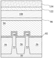
도 1은 일부 실시예에 따른 FinFET의 예를 입체도로 예시한다. FinFET는 기판(50)(예, 반도체 기판) 상에 핀(52)을 포함한다. 분리 영역(56)이 기판(50)에 배치되고, 인접한 분리 영역(56) 사이에서 위로 핀(52)이 돌출된다. 분리 영역(56)은 기판(50)으로부터 분리된 것으로 설명/예시되지만, 본 명세서에서 사용되는 "기판"이란 용어는 단지 반도체 기판을 지칭하거나 분리 영역을 포함하는 반도체 기판을 지칭하는 데 사용될 수 있다. 또한, 핀(52)은 기판(50)으로서 단일의 연속 재료로서 예시되어 있지만, 핀(52) 및/또는 기판(50)은 단일 재료 또는 복수의 종류의 재료를 포함할 수 있다. 이와 관련하여, 핀(52)은 인접하는 분리 영역(56) 사이에서 연장되는 부분을 지칭한다.1 illustrates an example of a FinFET in a stereoscopic view in accordance with some embodiments. A FinFET includes a
게이트 유전체 층(92)이 핀(52)의 측벽을 따라 그리고 핀의 상부 표면 위에 제공되고, 게이트 전극(94)이 게이트 유전체 층(92) 위에 제공된다. 소스/드레인 영역(82)이 게이트 유전체 층(92)과 게이트 전극(94)과 관련하여 핀(52)의 양측에 배치된다. 도 1은 이후의 도면에서 사용되는 기준 단면을 추가로 예시한다. A-A 단면은 게이트 전극(94)의 종축을 따라 그리고 예를 들어, FinFET의 소스/드레인 영역(82) 사이의 전류 흐름 방향에 수직인 방향으로 제공된다. B-B 단면은 A-A 단면에 수직하고, 핀(52)의 종축을 따라 그리고 예를 들어, FinFET의 소스/드레인 영역(82) 사이의 전류 흐름의 방향으로 제공된다. C-C 단면은 A-A 단면에 평행하고, FinFET의 소스/드레인 영역을 통해 연장된다. 후속 도면은 명확성을 위해 이들 참조 단면을 지칭한다.A gate
본 명세서에서 논의된 일부 실시예는 게이트-라스트 공정(gate-last process)을 이용하여 형성된 FinFET의 측면에서 논의된다. 다른 실시예에서, 게이트-퍼스트 공정(gate-first process)이 적용될 수 있다. 또한, 일부 실시예는 평면형 FET와 같은 평면형 디바이스에 사용되는 측면을 고려한다.Some embodiments discussed herein are discussed in terms of FinFETs formed using a gate-last process. In other embodiments, a gate-first process may be applied. Also, some embodiments contemplate aspects of use with planar devices, such as planar FETs.
도 2-28은 일부 실시예에 따른 FinFET의 제조의 중간 단계의 단면도를 포함한다. 도 2-7은 다수의 핀/FinFET를 제외하고, 도 1에 예시된 A-A 기준 단면을 예시한다. 도 8a, 9a, 10a, 11a, 12a, 13a, 14a, 15a, 24a, 25a, 26a 및 27a는 도 1에 예시된 A-A 기준 단면을 따라 예시되며, 도 8b, 9b, 10b, 11b, 12b, 13b, 14b, 14c, 15b, 16, 17, 18, 19, 20, 21, 22, 23a, 23b, 24b, 25b, 26b, 27b 및 28은 다수의 핀/FinFET을 제외하고 도 1에 예시된 유사한 B-B 단면을 따라 예시되어 있다. 도 10c 및 10d는 다수의 핀/FinFET를 제외하고 도 1에 예시된 C-C 기준 단면을 따라 예시되어 있다.2-28 include cross-sectional views of intermediate stages of fabrication of FinFETs in accordance with some embodiments. 2-7 illustrate the A-A reference cross-section illustrated in FIG. 1, excluding multiple Fin/FinFETs. 8a, 9a, 10a, 11a, 12a, 13a, 14a, 15a, 24a, 25a, 26a and 27a are illustrated along the A-A reference cross-section illustrated in FIG. 1, and FIGS. 8b, 9b, 10b, 11b, 12b, 13b , 14b, 14c, 15b, 16, 17, 18, 19, 20, 21, 22, 23a, 23b, 24b, 25b, 26b, 27b and 28 are similar B-B illustrated in FIG. 1 except for multiple Fin/FinFETs. Illustrated along the cross section. 10C and 10D are illustrated along the C-C reference cross section illustrated in FIG. 1 excluding multiple Fin/FinFETs.
도 2에서, 기판(50)이 제공된다. 기판(50)은 (예, p-형 또는 n-형 도펀트로) 도핑되거나 도핑되지 않을 수 있는 벌크 반도체, 반도체-온-절연체(SOI) 기판 등과 같은 반도체 기판일 수 있다. 기판(50)은 실리콘 웨이퍼와 같은 웨이퍼일 수 있다. 일반적으로, SOI 기판은 절연체 층 상에 형성된 반도체 재료층이다. 절연체 층은 예를 들어, 매립 산화물(BOX) 층, 실리콘 산화물 층 등일 수 있다. 절연체 층은 기판, 전형적으로 실리콘 또는 유리 기판 상에 제공된다. 다층 또는 구배 기판과 같은 다른 기판도 사용될 수 있다. 일부 실시예에서, 기판(50)의 반도체 재료는 실리콘; 게르마늄; 실리콘 탄화물, 갈륨 비소화물, 갈륨 인화물, 인듐 인화물, 인듐 비소화물 및/또는 인듐 안티몬화물을 포함하는 화합물 반도체; 실리콘-게르마늄, 갈륨 비소화물 인화물, 알루미늄 인듐 비소화물, 알루미늄 갈륨 비소화물, 갈륨 인듐 비소화물, 갈륨 인듐 인화물 및/또는 갈륨 인듐 비소화물 인화물을 포함하는 합금 반도체; 또는 이들의 조합을 포함할 수 있다.In Figure 2, a
기판(50)은 영역(50N) 및 영역(50P)을 포함한다. 영역(50N)은 n-형 FinFET 등의 NMOS 트랜지스터와 같은 n-형 디바이스를 형성하기 위한 영역일 수 있다. 영역(50P)은 p-형 FinFET 등의 PMOS 트랜지스터와 같은 p-형 디바이스를 형성하기 위한 영역일 수 있다. 영역(50N)은 (칸막이(51)에 의해 예시된 바와 같이) 영역(50P)으로부터 물리적으로 분리될 수 있고, 임의의 수의 디바이스 특징부(예, 다른 능동 디바이스, 도핑 영역, 분리 구조체 등)가 영역(50N)과 영역(50P) 사이에 배치될 수 있다.The
도 3에서, 핀(52)들이 기판(50)에 형성된다. 핀(52)은 반도체 스트립이다. 일부 실시예에서, 핀(52)은 기판(50)에 트렌치를 에칭함으로써 기판(50)에 형성될 수 있다. 에칭은 반응성 이온 에칭(RIE), 중성빔 에칭(NBE) 등등 또는 이들의 조합과 같은 임의의 허용 가능한 에칭 공정일 수 있다. 에칭은 이방성일 수 있다.In FIG. 3 ,
핀은 임의의 적절한 방법에 의해 패턴화될 수 있다. 예를 들어, 핀은 이중 패턴화 또는 다중 패턴화 공정을 포함하는 하나 이상의 포토리소그래피 공정을 이용하여 패턴화될 수 있다. 일반적으로, 이중 패턴화 또는 다중 패턴화 공정은 포토리소그래피와 자체 정렬 공정을 결합하여, 예컨대 단일의 직접 포토리소그래피 공정을 이용하여 얻을 수 있는 것보다 작은 피치를 가지는 패턴을 형성할 수 있다. 예를 들어, 일 실시예에서, 희생층이 기판 위에 형성되고 포토리소그래피 공정에 의해 패턴화된다. 자체 정렬 공정을 이용하여 패턴화된 희생층과 나란히 희생층이 형성된다. 이어서 희생층을 제거한 후, 나머지 스페이서를 사용하여 핀을 패턴화시킬 수 있다. 일부 실시예에서, 마스크(또는 다른 층)가 핀(52) 상에 남겨질 수 있다.The fins may be patterned by any suitable method. For example, the fins may be patterned using one or more photolithography processes including double patterning or multi-patterning processes. In general, double-patterning or multi-patterning processes can combine photolithography and self-alignment processes to form patterns with smaller pitches than can be obtained using, for example, a single direct photolithography process. For example, in one embodiment, a sacrificial layer is formed over a substrate and patterned by a photolithography process. A sacrificial layer is formed alongside the patterned sacrificial layer using a self-alignment process. After the sacrificial layer is then removed, the remaining spacer can be used to pattern the fin. In some embodiments, a mask (or other layer) may be left over the
도 4에서, 절연 재료(54)가 기판(50) 위에 그리고 인접하는 핀(52) 사이에 형성된다. 절연 재료(54)는 실리콘 산화물과 같은 산화물, 질화물, 등등 또는 이들의 조합일 수 있으며, 고밀도 플라즈마 화학적 기상 성막(HDP-CVD), 유동성 CVD(FCVD)(예, 원격 플라즈마 시스템에서의 CVD-기반 재료 성막 및 산화물과 같은 다른 재료로의 변환을 위한 후경화(post curing)) 등등 또는 이들의 조합에 의해 형성될 수 있다. 임의의 허용 가능한 공정에 의해 형성된 다른 절연 재료가 사용될 수 있다. 예시된 실시예에서, 절연 재료(54)는 FCVD 공정에 의해 형성된 실리콘 산화물이다. 일단 절연 재료가 형성되면 어닐링 공정이 수행될 수 있다. 일 실시예에서, 절연 재료(54)는 과잉의 절연 재료(54)가 핀(52)을 덮도록 형성된다. 절연 재료(54)는 단일 층으로서 예시되어 있지만, 일부 실시예는 다중 층을 사용할 수 있다. 예를 들어, 일부 실시예에서, 기판(50)의 표면 및 핀(52)을 따라 라이너(미도시)가 먼저 형성될 수 있다. 이후, 전술한 것과 같은 충전 재료가 라이너 위에 형성될 수 있다.In FIG. 4 , an insulating
도 5에서, 핀(52) 위의 과잉의 절연 재료(54)를 제거하기 위해 절연 재료(54)에 대해 제거 공정이 적용된다. 일부 실시예에서, 화학적 기계적 연마(CMP), 에치백 공정, 이들의 조합 등등과 같은 평탄화 공정이 적용될 수 있다. 평탄화 공정은 평탄화 공정이 완료된 후 핀(52) 및 절연 재료(54)의 상부 표면이 동평면이 되도록 핀(52)을 노출시킨다. 마스크가 핀(52) 상에 남아 있는 실시예에서, 평탄화 공정은 마스크 또는 핀(52)의 상부 표면 및 절연 재료(54)가 평탄화 공정의 완료 후에 동평면이 되도록 마스크를 노출시키거나 마스크를 제거할 수 있다.In FIG. 5 , a removal process is applied to insulating
도 6에서, 절연 재료(54)는 얕은 트렌치 분리(STI) 영역(56)을 형성하도록 오목화된다. 절연 재료(54)는 영역(50N) 및 영역(50P) 내의 핀(52)의 상부가 인접한 STI 영역(56) 사이에서 돌출되도록 오목화된다. 또한, STI 영역(56)의 상부면은 도시된 바와 같은 평탄면, 볼록면, 오목면(예, 접시형) 또는 이들의 조합을 가질 수 있다. STI 영역(56)의 상부면은 적절한 에칭에 의해 평탄하고 볼록하고 및/또는 오목하게 형성될 수 있다. STI 영역(56)은 절연 재료(54)의 재료에 대해 선택적인 것과 같은 허용 가능한 에칭 공정을 이용하여 오목화될 수 있다(예를 들어, 핀(52)의 재료보다 빠른 속도로 절연 재료(54)의 재료를 에칭). 예를 들어, 희석된 불화수소(dHF) 산 등을 사용한 산화물 제거가 적용될 수 있다.In FIG. 6 , insulating
도 2-6과 관련하여 설명된 공정은 핀(52)을 형성할 수 있는 방법의 단지 하나의 예이다. 일부 실시예에서, 핀은 에피택셜 성장 공정에 의해 형성될 수 있다. 예를 들어, 유전체 층이 기판(50)의 상부 표면 위에 형성될 수 있고, 트렌치가 유전체 층을 통해 에칭되어 하부의 기판(50)을 노출시킬 수 있다. 트렌치 내에 호모에피택셜 구조체가 에피택셜 성장될 수 있고, 호모에피택셜 구조체가 유전체 층으로부터 돌출하여 핀을 형성하도록 유전체 층이 오목화될 수 있다. 추가로, 일부 실시예에서, 헤테로에피택셜 구조체가 핀(52)에 적용될 수 있다. 예를 들어,도 5의 핀(52)이 오목화될 수 있고, 핀(52)과 상이한 재료가 오목화된 핀(52) 위에 에피택셜 성장될 수 있다. 이러한 실시예에서, 핀(52)은 오목화된 재료뿐만 아니라 해당 오목화된 재료 위에 배치된 에피택셜 성장 재료를 포함한다. 또 다른 실시예에서, 유전체 층이 기판(50)의 상부 표면 위에 형성될 수 있고, 트렌치가 유전체 층을 통해 에칭될 수 있다. 이후, 헤테로에피택셜 구조체가 기판(50)과 다른 재료를 사용하여 트렌치 내에서 에피택셜 성장될 수 있으며, 헤테로에피택셜 구조체가 유전체 층으로부터 돌출하여 핀(52)을 형성하도록 유전체 층이 오목화될 수 있다. 호모에피택셜 또는 헤테로에피택셜 구조체가 에피택셜 성장되는 일부 실시예에서, 에피택셜 성장된 재료는 주입 전후에 배제될 수 있는 성장 중에 인-시튜 도핑될 수 있지만, 인-시튜 및 주입 도핑은 함께 사용될 수 있다.The process described with respect to FIGS. 2-6 is just one example of how
또한, 영역(50P)(예, PMOS 영역)의 재료와 다른 영역(50N)(예, NMOS 영역)의 재료를 에피택셜 성장시키는 것이 유리할 수 있다. 다양한 실시예에서, 핀(52)의 상부는 실리콘-게르마늄(SixGe1-x, 여기서 x는 0 내지 1의 범위일 수 있음), 실리콘 탄화물, 순수한 또는 실질적으로 순수한 게르마늄, III-V족 화합물 반도체, II-VI족 화합물 반도체 등으로부터 형성될 수 있다. 예를 들어, III-V족 화합물 반도체를 형성하는 데 사용 가능한 재료는 한정되는 것은 아니지만, 인듐 비소화물, 알루미늄 비소화물, 갈륨 비소화물, 인듐 인화물, 갈륨 질화물, 인듐 갈륨 비소화물, 인듐 알루미늄 비소화물, 갈륨 안티몬화물, 알루미늄 안티몬화물, 알루미늄 인화물, 갈륨 인화물 등을 포함한다.It may also be advantageous to epitaxially grow the material of
또한, 도 6에서, 핀(52) 및/또는 기판(50)에 적절한 우물(미도시)이 형성될 수 있다. 일부 실시예에서, P-형 우물이 영역(50N)에 형성될 수 있고, N-형 우물이 영역(50P)에 형성될 수 있다. 일부 실시예에서, P-형 우물 또는 N-형 우물은 영역(50N) 및 영역(50P) 모두에 형성된다.Also in FIG. 6 , suitable wells (not shown) may be formed in
상이한 우물 유형을 가지는 실시예에서, 영역(50N) 및 영역(50P)에 대한 상이한 주입 단계가 포토레지스트 또는 다른 마스크(미도시)를 사용하여 달성될 수 있다. 예를 들어, 영역(50N)에서 핀(52) 및 STI 영역(56) 위에 포토레지스트가 형성될 수 있다. 포토레지스트는 PMOS 영역과 같은 기판(50)의 영역(50P)을 노출 시키도록 패턴화된다. 포토레지스트는 스핀-온 기술을 이용하여 형성될 수 있고, 허용 가능한 포토리소그래피 기술을 이용하여 패턴화될 수 있다. 일단 포토레지스트가 패턴화되면, n-형 불순물 주입이 영역(50P)에서 수행되고, 포토레지스트는 n-형 불순물이 NMOS 영역과 같은 영역(50N) 내로 주입되는 것을 실질적으로 방지하는 마스크로서 작용할 수 있다. n-형 불순물은 1018 cm-3 이하, 예컨대 약 1016 cm-3 내지 약 1018 cm-3의 농도로 영역에 주입되는 인, 비소, 안티몬 등일 수 있다. 주입 후, 예를 들어, 허용 가능한 애싱(ashing) 공정에 의해 포토레지스트가 제거된다.In embodiments having different well types, different implant steps for
영역(50P)의 주입 후에, 영역(50P)의 핀(52) 및 STI 영역(56) 위에 포토레지스트가 형성된다. 포토레지스트는 NMOS 영역과 같은 기판(50)의 영역(50N)을 노출시키도록 패턴화된다. 포토레지스트는 스핀-온 기술을 이용하여 형성될 수 있고, 허용 가능한 포토리소그래피 기술을 이용하여 패턴화될 수 있다. 일단 포토레지스트가 패턴화되면, p-형 불순물 주입이 영역(50N)에서 수행될 수 있고, 포토레지스트는 p-형 불순물이 PMOS 영역과 같은 영역(50P)으로 주입되는 것을 실질적으로 방지하는 마스크로서 작용할 수 있다. p-형 불순물은 1018 cm-3 이하, 예컨대 약 1016 cm-3 내지 약 1018 cm-3의 농도로 영역에 주입되는 붕소, 불화 붕소, 인듐 등일 수 있다. 주입 후에, 예를 들어, 허용 가능한 애싱 공정에 의해 포토레지스트가 제거될 수 있다.After implantation of
영역(50N) 및 영역(50P)의 주입 후에, 주입 손상을 복구하고 주입된 p-형 및/또는 n-형 불순물을 활성화시키기 위해 어닐링이 수행될 수 있다. 일부 실시예에서, 에피택셜 핀의 성장된 재료는 주입을 배제할 수 있는 성장 중에 인-시튜 도핑될 수 있지만, 인-시튜 및 주입 도핑은 함께 사용될 수 있다.After implantation of
도 7에서, 더미 유전체 층(60)이 핀(52) 상에 형성된다. 더미 유전체 층(60)은 예를 들어, 실리콘 산화물, 실리콘 질화물, 또는 이들의 조합 등일 수 있고, 허용 가능한 기술에 따라 성막되거나 열적으로 성장될 수 있다. 더미 게이트 층(62)이 더미 유전체 층(60) 위에 형성되고, 마스크 층(64)이 더미 게이트 층(62) 위에 형성된다. 더미 게이트 층(62)은 더미 유전체 층(60) 위에 성막된 후, 예컨대 CMP에 의해 평탄화될 수 있다. 마스크 층(64)은 더미 게이트 층(62) 위에 성막될 수 있다. 더미 게이트 층(62)은 전도성 또는 비전도성 재료일 수 있고, 비정질 실리콘, 다결정 실리콘(폴리실리콘), 다결정 실리콘-게르마늄(poly-SiGe), 금속 질화물, 금속 실리사이드, 금속 산화물 및 금속을 포함하는 그룹에서 선택될 수 있다. 더미 게이트 층(62)은 물리적 기상 성막(PVD), CVD, 스퍼터링 성막, 또는 선택된 재료를 성막하기 위해 당업계에 공지되고 사용되는 다른 기술에 의해 성막될 수 있다. 더미 게이트 층(62)은 분리 영역의 에칭으로부터 높은 에칭 선택도를 갖는 다른 재료로 형성될 수 있다. 마스크 층(64)은 예를 들어, 실리콘 질화물, 실리콘 산질화물 등을 포함할 수 있다. 이 예에서, 단일 더미 게이트 층(62) 및 단일 마스크 층(64)이 영역(50N) 및 영역(50P)에 걸쳐 형성된다. 더미 유전체 층(60)은 단지 예시의 목적으로 핀(52)만을 덮는 것으로 예시되어 있다. 일부 실시예에서, 더미 유전체 층(60)은 더미 유전체 층(60)이 STI 영역(56)을 덮어서 더미 게이트 층(62)과 STI 영역(56) 사이에서 연장되도록 성막될 수 있다.In FIG. 7 , a
도 8a-15b는 실시예 디바이스의 제조에서의 다양한 추가의 단계를 예시한다. 도 8a-15b는 영역(50N) 및 영역(50P) 중 하나의 특징부를 예시한다. 예를 들어, 도 8a-15b에 예시된 구조체는 영역(50N) 및 영역(50P) 모두에 적용 가능할 수 있다. 영역(50N) 및 영역(50P)의 구조체에서의 차이점(있는 경우)은 각 도면에 수반하는 텍스트에 기술되어 있다.8A-15B illustrate various additional steps in the fabrication of example devices. 8A-15B illustrate features of one of
도 8a 및 도 8b에서, 마스크 층(64)(도 7 참조)은 마스크(74)를 형성하기 위해 허용 가능한 포토리소그래피 및 에칭 기술을 이용하여 패턴화될 수 있다. 마스크(74)의 패턴은 이후 더미 게이트 층(62)으로 전사될 수 있다. 일부 실시예(미도시)에서, 마스크(74)의 패턴은 또한 더미 게이트(72)를 형성하기 위해 허용 가능한 에칭 기술에 의해 더미 유전체 층(60)으로 전사될 수 있다. 더미 게이트(72)는 핀(52)의 각각의 채널 영역(58)을 커버한다. 마스크(74)의 패턴은 더미 게이트(72) 각각을 인접한 더미 게이트로부터 물리적으로 분리하는 데 사용될 수 있다. 더미 게이트(72)는 또한 각각의 에피택셜 핀(52)의 길이 방향에 실질적으로 수직인 길이 방향을 가질 수 있다.In FIGS. 8A and 8B , mask layer 64 (see FIG. 7 ) may be patterned using acceptable photolithography and etching techniques to form
또한 도 8a 및 도 8b에서, 게이트 밀봉 스페이서(80)가 더미 게이트(72), 마스크(74) 및/또는 핀(52)의 노출된 표면 상에 형성될 수 있다. 열 산화 또는 성막에 이은 이방성 에칭에 의해 게이트 밀봉 스페이서(80)가 형성될 수 있다. 게이트 밀봉 스페이서(80)는 실리콘 산화물, 실리콘 질화물, 실리콘 산질화물 등으로 형성될 수 있다.Also in FIGS. 8A and 8B ,
게이트 밀봉 스페이서(80)의 형성 후에, 저농도 도핑된 소스/드레인(LDD) 영역(명확하게 도시하지 않음)을 위한 주입이 수행될 수 있다. 상이한 디바이스 유형을 가지는 실시예에서, 도 6에서 전술한 주입과 유사하게, 포토레지스트와 같은 마스크가 영역(50P)을 노출시키면서 영역(50N) 위에 형성될 수 있으며, 적절한 유형(예를 들어, p-형)의 불순물이 영역(50P)의 노출된 핀(52)에 주입될 수 있다. 이후 마스크는 제거될 수 있다. 이어서, 포토레지스트와 같은 마스크가 영역(50N)을 노출시키면서 영역(50P) 위에 형성될 수 있고, 적절한 유형(예를 들어, n-형)의 불순물이 영역(50N)의 노출된 핀(52)에 주입될 수 있다. 이후 마스크는 제거될 수 있다. n-형 불순물은 전술한 n-형 불순물 중 임의의 것일 수 있고, p-형 불순물은 전술한 p-형 불순물 중 임의의 것일 수 있다. 저농도 도핑된 소스/드레인 영역은 약 1015 cm-3 내지 약 1019 cm-3의 불순물 농도를 가질 수 있다. 주입 손상을 복구하고 주입된 불순물을 활성화시키기 위해 어닐링이 적용될 수 있다.After formation of the
도 9a 및 도 9b에서, 게이트 스페이서(86)가 더미 게이트(72) 및 마스크(74)의 측벽을 따라 게이트 밀봉 스페이서(80) 상에 형성된다. 게이트 스페이서(86)는 절연 재료를 동형으로(conformally) 성막한 후 이방성 에칭을 행함으로써 형성될 수 있다. 게이트 스페이서(86)의 절연 재료는 실리콘 산화물, 실리콘 질화물, 실리콘 산질화물, 실리콘 탄질화물, 이들의 조합 등일 수 있다.9A and 9B,
상기 개시 내용은 일반적으로 스페이서 및 LDD 영역을 형성하는 공정을 설명하는 것을 알아야 한다. 다른 공정 및 순서가 적용될 수 있다. 예를 들어, 더 적거나 추가의 스페이서를 사용할 수 있으며, 상이한 단계 순서를 적용할 수 있으며(예, 게이트 밀봉 스페이서(80)는 게이트 스페이서(86)를 형성하기 전에 에칭되지 않아서 "L-형" 게이트 밀봉 스페이서를 형성할 수 있음), 스페이서를 형성 및 제거할 수 있으며, 및/또는 기타의 경우가 있을 수 있다. 예를 들어, n-형 디바이스를 위한 LDD 영역은 게이트 밀봉 스페이서(80)를 형성하기 전에 형성될 수 있는 반면, p-형 디바이스를 위한 LDD 영역은 게이트 밀봉 스페이서(80)를 형성한 후에 형성될 수 있다.It should be noted that the above disclosure generally describes the process of forming spacers and LDD regions. Other processes and sequences may be applied. For example, fewer or more spacers may be used, a different order of steps may be applied (e.g.,
도 10a 및 도 10b에서, 일부 실시예에 따라, 에피택셜 소스/드레인 영역(82)이 핀(52)에 형성된다. 일부 경우에, 에피택셜 소스/드레인 영역(82)은 각각의 채널 영역(58)에 응력을 가하도록 형성되어 성능을 향상시킬 수 있다. 에피택셜 소스/드레인 영역(82)은 각각의 더미 게이트(72)가 각각의 인접한 쌍의 에피택셜 소스/드레인 영역(82) 사이에 배치되도록 핀(52)에 형성된다. 일부 실시예에서, 에피택셜 소스/드레인 영역(82)은 핀(52) 내로 연장될 수 있으며, 또한 핀(52)을 관통할 수 있다. 일부 실시예에서, 게이트 스페이서(86)는 에피택셜 소스/드레인 영역(82)이 최종 FinFET의 후속으로 형성되는 게이트를 단락시키지 않도록 적절한 측방 거리만큼 더미 게이트(72)로부터 에피택셜 소스/드레인 영역(82)을 분리하는 데 사용된다.10A and 10B, epitaxial source/
영역(50N), 예를 들어 NMOS 영역의 에피택셜 소스/드레인 영역(82)은 영역(50P), 예를 들어 PMOS 영역을 마스킹하고 영역(50N) 내의 핀(52)의 소스/드레인 영역을 에칭하여 핀(52)에 리세스를 형성하는 것에 의해 형성될 수 있다. 이후, 영역(50N)의 에피택셜 소스/드레인 영역(82)은 리세스 내에서 에피택셜 성장된다. 에피택셜 소스/드레인 영역(82)은 n-형 FinFET에 적합한 것과 같은 임의의 허용 가능한 재료를 포함할 수 있다. 예를 들어, 핀(52)이 실리콘인 경우, 영역(50N)의 에피택셜 소스/드레인 영역(82)은 채널 영역(58)에 인장 변형을 가하는 실리콘, 실리콘 탄화물, 인-도핑된 실리콘 탄화물, 실리콘 인화물 등과 같은 재료를 포함할 수 있다. 영역(50N)의 에피택셜 소스/드레인 영역(82)은 핀(52)의 각각의 표면으로부터 상승된 표면을 가질 수 있고, 패싯(facet)을 가질 수 있다.Epitaxial source/
예를 들어, PMOS 영역과 같은 영역(50P)의 에피택셜 소스/드레인 영역(82)은 영역(50N), 예를 들어 NMOS 영역을 마스킹하고 영역(50P) 내의 핀(52)의 소스/드레인 영역을 에칭하여 핀(52)에 리세스를 형성하는 것에 의해 형성될 수 있다. 이후, 영역(50P)의 에피택셜 소스/드레인 영역(82)은 리세스 내에서 에피택셜 성장된다. 에피택셜 소스/드레인 영역(82)은 p-형 FinFET에 적절한 것과 같은 임의의 허용 가능한 재료를 포함할 수 있다. 예를 들어, 핀(52)이 실리콘인 경우, 영역(50P)의 에피택셜 소스/드레인 영역(82)은 채널 영역(58)에 압축 변형을 가하는 실리콘-게르마늄, 붕소-도핑된 실리콘-게르마늄, 게르마늄, 게르마늄 주석 등과 같은 재료를 포함할 수 있다. 영역(50P)의 에피택셜 소스/드레인 영역(82)은 또한 핀(52)의 각각의 표면으로부터 상승된 표면을 가질 수 있고, 패싯을 가질 수 있다.For example, epitaxial source/
에피택셜 소스/드레인 영역(82) 및/또는 핀(52)은 저농도 도핑된 소스/드레인 영역을 형성하기 위한 전술한 공정과 유사하게 소스/드레인 영역을 형성하는 도펀트가 주입된 후 어닐링될 수 있다. 소스/드레인 영역은 약 1019 cm-3 내지 약 1021 cm-3의 불순물 농도를 가질 수 있다. 소스/드레인 영역을 위한 n-형 및/또는 p-형 불순물은 전술한 불순물 중 임의의 것일 수 있다. 일부 실시예에서, 에피택셜 소스/드레인 영역(82)은 성장 중에 인-시튜 도핑될 수 있다.Epitaxial source/
영역(50N) 및 영역(50P)에 에피택셜 소스/드레인 영역(82)을 형성하는 데 에피택시 공정을 적용한 결과로서, 에피택셜 소스/드레인 영역의 상부 표면은 핀(52)의 측벽 너머 측방 외측으로 확장되는 패싯을 포함한다. 일부 실시예에서, 이러한 패싯은 동일한 FinFET의 인접한 소스/드레인 영역(82)이 도 10c에 예시된 바와 같이 병합되게 한다. 다른 실시예에서, 인접한 소스/드레인 영역(82)은 도 10d에 의해 예시된 바와 같이 에피택시 공정이 완료된 후에 분리된 상태로 유지된다. 도 10c 및 도 10d에 예시된 실시예에서, 게이트 스페이서(86)는 STI 영역(56) 위로 연장되는 핀(52)의 측벽의 일부를 덮도록 형성되어 에피택셜 성장을 차단한다. 일부 다른 실시예에서, 게이트 스페이서(86)를 형성하는 데 사용되는 스페이서 에칭은 에피택셜 성장 영역이 STI 영역(56)의 표면으로 연장될 수 있도록 스페이서 재료를 제거하도록 조정될 수 있다.As a result of applying an epitaxial process to form epitaxial source/
도 11a 및 도 11b에서, 일부 실시예에 따르면, 제1 층간 유전체(ILD)(88)가 도 10a 및 도 10b에 예시된 구조체 위에 성막된다. 제1 ILD(88)는 유전체 재료로 형성될 수 있으며, CVD, 플라즈마 강화 CVD(PECVD) 또는 FCVD와 같은 임의의 적절한 방법에 의해 성막될 수 있다. 유전체 재료는 포스포-실리케이트 유리(PSG), 보로-실리케이트 유리(BSG), 붕소-도핑된 포스포-실리케이트 유리(BPSG), 도핑되지 않은 실리케이트 유리(USG) 등을 포함할 수 있다. 임의의 허용 가능한 공정에 의해 형성된 다른 절연 재료가 사용될 수 있다. 일부 실시예에서, 접촉 에칭 정지층(CESL)(87)이 제1 ILD(88)와 에피택셜 소스/드레인 영역(82), 마스크(74) 및 게이트 스페이서(86) 사이에 배치된다. CESL(87)은 실리콘 질화물, 실리콘 산화물, 실리콘 산질화물 등과 같은 유전체 재료를 포함할 수 있으며, 상부의 제1 ILD(88)의 재료와 상이한 에칭 속도를 가질 수 있다. 일부 실시예에서, CESL(87)은 약 2 nm 내지 약 5 nm, 예컨대, 약 3 nm의 두께를 가지도록 형성될 수 있다. 일부 경우에, CESL(87)의 두께를 조절하는 것은 소스/드레인 접촉부(118)의 크기(예, 폭 또는 높이) 및/또는 후속으로 형성된 에어 갭(120)의 크기(예, 폭 또는 높이)를 조절할 수 있다(도 17-22 참조).11A and 11B, in accordance with some embodiments, a first interlayer dielectric (ILD) 88 is deposited over the structure illustrated in FIGS. 10A and 10B. The
도 12a 및 도 12b에서, 더미 게이트(72) 또는 마스크(74)의 상부면과 제1 ILD(88)의 상부면을 동평면화하기 위해 CMP와 같은 평탄화 공정이 수행될 수 있다. 평탄화 공정에 의해 더미 게이트(72) 상의 마스크(74) 및 마스크(74)의 측벽을 따른 게이트 밀봉 스페이서(80) 및 게이트 스페이서(86)의 일부가 제거될 수 있다. 평탄화 공정 후, 더미 게이트(72), 게이트 밀봉 스페이서(80), 게이트 스페이서(86) 및 제1 ILD(88)의 상부면은 동일 높이이다. 따라서, 더미 게이트(72)의 상부면은 제1 ILD(88)를 통해 노출된다. 일부 실시예에서, 마스크(74)는 남겨질 수 있으며, 이 경우, 평탄화 공정에 의해 제1 ILD(88)의 상부면과 마스크(74)의 상부면이 동평면화된다.12A and 12B, a planarization process such as CMP may be performed to coplanarize the upper surface of the
도 13a 및 도 13b에서, 더미 게이트(72) 및 마스크(74)(존재하는 경우)는 하나 이상의 에칭 단계에서 제거되어 리세스(90)가 형성된다. 리세스(90) 내의 더미 유전체 층(60)의 일부가 또한 제거될 수 있다. 일부 실시예에서, 더미 게이트(72)만이 제거되고 더미 유전체 층(60)은 남겨져서 리세스(90)에 의해 노출된다. 일부 실시예에서, 더미 유전체 층(60)은 다이의 제1 영역(예, 코어 로직 영역)의 리세스(90)로부터 제거되고, 다이의 제2 영역(예, 입력/출력 영역)의 리세스(90)에 잔류한다. 일부 실시예에서, 더미 게이트(72)는 이방성 건식 에칭 공정에 의해 제거된다. 예를 들어, 에칭 공정은 제1 ILD(88), 게이트 스페이서(86) 또는 CESL(87)을 에칭하지 않고 더미 게이트(72)를 선택적으로 에칭하는 일종 이상의 반응 가스를 사용하는 건식 에칭 공정을 포함할 수 있다. 각각의 리세스(90)는 각각의 핀(52)의 채널 영역을 노출시키고 및/또는 채널 영역 위에 배치된다. 각각의 채널 영역(58)은 인접하는 쌍의 에피택셜 소스/드레인 영역(82)의 사이에 배치된다. 제거 중에, 더미 유전체 층(60)은 더미 게이트(72)가 에칭될 때 에칭 정지층으로서 사용될 수 있다. 더미 유전체 층(60)은 더미 게이트(72)의 제거 후에 선택적으로 제거될 수 있다.13A and 13B,
도 14a 및 도 14b에서, 게이트 유전체 층(92) 및 게이트 전극(94)이 대체 게이트를 위해 형성된다. 도 14c는 도 14b의 영역(89)의 상세도를 예시한다. 게이트 유전체 층(92)은 리세스(90) 내에 예컨대, 핀(52)의 상부면 및 측벽 및 게이트 밀봉 스페이서(80)/게이트 스페이서(86)의 측벽 상에 동형으로 성막된다. 게이트 유전체 층(92)은 또한 제1 ILD(88)의 상부면 상에 형성될 수 있다. 일부 실시예에 따르면, 게이트 유전체 층(92)은 실리콘 산화물, 실리콘 질화물 또는 이들의 다층을 포함한다. 일부 실시예에서, 게이트 유전체 층(92)은 하이-k 유전체 재료를 포함하고, 이들 실시예에서, 게이트 유전체 층(92)은 약 7.0보다 큰 k-값을 가질 수 있고, 하프늄, 알루미늄, 지르코늄, 란탄, 망간, 바륨, 티타늄, 납 및 이들의 조합의 금속 산화물 또는 실리케이트를 포함할 수 있다. 게이트 유전체 층(92)의 형성 방법은 분자빔 성막(MBD), ALD, PECVD 등을 포함할 수 있다. 더미 유전체 층(60)의 일부가 리세스(90)에 잔류하는 실시예에서, 게이트 유전체 층(92)은 더미 유전체 층(60)의 재료(예, 실리콘 산화물)를 포함한다.14A and 14B, a
게이트 전극(94)은 각각 게이트 유전체 층(92) 위에 성막되고, 리세스(90)의 나머지 부분을 채운다. 게이트 전극(94)은 티타늄 질화물, 티타늄 산화물, 탄탈 질화물, 탄탈 탄화물, 코발트, 루테늄, 알루미늄, 텅스텐, 이들의 조합 또는 이들의 다층과 같은 금속 함유 재료를 포함할 수 있다. 예를 들어, 단일층 게이트 전극(94)이 도 14b에 예시되어 있지만, 게이트 전극(94)은 도 14c에 예시된 바와 같이 임의의 수의 라이너 층(94A), 임의의 수의 일함수 조정층(94B) 및 충전 재료(94C)를 포함할 수 있다. 리세스(90)의 충전 후에, 게이트 유전체 층(92)의 과잉의 부분과 게이트 전극(94)의 재료를 제거하기 위해 CMP와 같은 평탄화 공정이 수행될 수 있으며, 여기서 상기 과잉의 부분은 ILD(88)의 상부면 위에 있다. 게이트 전극(94) 및 게이트 유전체 층(92)의 재료의 나머지 부분은 최종 FinFET의 대체 게이트를 형성한다. 게이트 전극(94) 및 게이트 유전체 층(92)은 집합적으로 "게이트 스택"으로 지칭될 수 있다. 게이트 및 게이트 스택은 핀(52)의 채널 영역(58)의 측벽을 따라 연장될 수 있다.
영역(50N) 및 영역(50P)에 게이트 유전체 층(92)의 형성은 각 영역의 게이트 유전체 층(92)이 동일한 재료로 형성되도록 동시에 일어날 수 있으며, 게이트 전극(94)의 형성은 각 영역의 게이트 전극(94)이 동일한 재료로 형성되도록 동시에 일어날 수 있다. 일부 실시예에서, 각 영역의 게이트 유전체 층(92)은 별개의 공정에 의해 형성될 수 있어서, 게이트 유전체 층(92)은 다른 재료일 수 있고 및/또는 각 영역의 게이트 전극(94)은 별개 공정에 의해 형성될 수 있어서, 게이트 전극(94)은 상이한 재료일 수 있다. 별개의 공정을 사용할 때 적절한 영역을 마스킹하고 노출시키기 위해 다양한 마스킹 단계가 적용될 수 있다.Formation of
도 15a 및 도 15b에서, 일부 실시예에 따르면, 제2 ILD(108)가 제1 ILD(88) 위에 성막된다. 일부 실시예에서, 제2 ILD(108)는 유동성 CVD 방법에 의해 형성된 유동성 필름이다. 일부 실시예에서, 제2 ILD(108)는 PSG, BSG, BPSG, USG, 실리콘 산화물 등과 같은 유전체 재료로 형성되고, CVD, PECVD 등과 같은 임의의 적절한 방법에 의해 성막될 수 있다. 제2 ILD(108)의 표면을 평탄화하기 위해 CMP와 같은 평탄화 공정이 수행될 수 있다. 일부 실시예에서, 제2 ILD(108)는 약 10 nm 내지 약 30 nm의 두께(T1)를 가지도록 형성될 수 있지만, 다른 두께도 가능하다. 15A and 15B, a
일부 실시예에 따르면, 하드 마스크(96)가 제2 ILD(108)의 성막 이전의 구조체 위에 성막된다. 하드 마스크(96)는 실리콘 질화물, 실리콘 산질화물 등과 같은 유전체 재료의 하나 이상의 층을 포함할 수 있으며, 상부의 제2 ILD(108)의 재료와 상이한 에칭 속도를 가질 수 있다. 일부 실시예에서, 하드 마스크(96)는 약 2 nm 내지 약 4 nm의 두께를 가지도록 형성될 수 있다. 일부 실시예에서, 하드 마스크(96)는 CESL(87)과 동일한 재료로 형성되거나 CESL(87)과 대략 동일한 두께를 가지도록 형성된다. 후속으로 형성된 소스/드레인 접촉부(118)(도 20 참조)가 하드 마스크(96) 및 CESL(87)을 관통하여 에피택셜 소스/드레인 영역(82)의 상부 표면과 접촉하며, 게이트 접촉부(132)(도 27a 참조)가 하드 마스크(96)를 관통하여 게이트 전극(94)의 상부 표면과 접촉한다.In accordance with some embodiments, a
도 16-22는 일부 실시예에 따라 에어 갭(120)(도 22 참조)에 접촉된 소스/드레인 접촉부(118)의 형성에서의 중간 단계를 예시한다. 소스/드레인 접촉부(118)는 에피택셜 소스/드레인 영역(82)과 물리적 및 전기적으로 접촉한다. 소스/드레인 접촉부(118)는 "접촉부(118)" 또는 "콘택트 플러그(118)"로도 지칭될 수 있다. 명확성을 위해, 도 16-22는 도 15b의 영역(111)의 상세도로서 도시되어 있다. 도 16은 도 15b에 도시된 동일한 구조체의 영역(111)을 예시한다.16-22 illustrate intermediate steps in the formation of source/
도 17에서, 일부 실시예에 따라, 에피택셜 소스/드레인 영역(82)을 노출시키도록 제1 ILD(88) 및 제2 ILD(108)에 개구(110)가 형성된다. 개구(110)는 적절한 포토리소그래피 및 에칭 기술을 이용하여 형성될 수 있다. 예를 들어, 포토레지스트(예, 단일층 또는 다층 포토레지스트 구조체)가 제2 ILD(108) 위에 형성될 수 있다. 이어서, 포토레지스트는 개구(110)에 대응하는 영역에서 제2 ILD(108)를 노출시키도록 패턴화될 수 있다. 이어서, 패턴화된 포토레지스트를 에칭 마스크로 사용하여 개구(110)를 에칭하기 위해 적절한 에칭 공정이 수행될 수 있다. 하나 이상의 에칭 공정은 습식 에칭 공정 및/또는 건식 에칭 공정을 포함할 수 있다. 일부 실시예에서, 개구(110)를 형성할 때, CESL(87) 및/또는 하드 마스크(96)가 에칭 정지층으로서 사용될 수 있다. 일부 실시예에서, 에피택셜 소스/드레인 영역(82) 위로 연장되는 CESL(87)의 일부도 역시 제거될 수 있다. 개구가 CESL(87)을 통해 연장되는 일부 실시예에서, 개구(110)은 에피택셜 소스/드레인 영역(82)의 상부 표면 아래로 에피택셜 소스/드레인 영역(82) 내로 연장될 수 있다. 일부 실시예에서, 하나 이상의 에칭 공정에 의해 제1 ILD(88)의 재료가 제거되어 CESL(87)을 노출시킬 수 있으며, 에피택셜 소스/드레인 영역(82) 위의 CESL(87)의 일부가 부분적으로 에칭될 수 있다. 개구(110)는 도 17에 예시된 바와 같이 테이퍼진 측벽을 가질 수 있거나, 상이한 프로파일의 측벽(예, 수직 측벽)을 가질 수 있다. 일부 실시예에서, 개구(110)는 약 10 nm 내지 약 30 nm의 폭(W1)을 가질 수 있지만, 다른 폭도 가능하다. 폭(W1)은 개구(110)의 상부, 개구(110)의 하부, 또는 임의의 다른 위치에서 개구(110)에 걸쳐 측정될 수 있다. 경우에 따라, 폭(W1)의 조절에 의해, 소스/드레인 접촉부(118)의 크기 및/또는 이후에 형성된 에어 갭(120)의 크기를 조절할 수 있다(도 22 참조).In FIG. 17 ,
도 18에서, 일부 실시예에 따라, 더미 스페이서 층(112)이 개구(110) 위에 형성된다. 일부 실시예에서, 에피택셜 소스/드레인 영역(82) 위의 CESL(87)을 제거하기 위해 에칭 공정이 먼저 수행된다. 에칭 공정은 예를 들어, 이방성 건식 에칭 공정을 포함할 수 있다. 에칭 공정은 에피택셜 소스/드레인 영역(82)의 상부 표면 아래로 그리고 에피택셜 소스/드레인 영역(82) 내로 개구(110)를 연장시킬 수 있다. 이후, 더미 스페이서 층(112)은 일부 실시예에서 제2 ILD(108), CESL(87) 및 에피택셜 소스/드레인 영역(82) 위로 연장되는 블랭킷 층으로서 형성될 수 있다. 더미 스페이서 층(112)은 실리콘, 폴리 실리콘, 비정질 실리콘 등등 또는 이들의 조합과 같은 재료를 포함할 수 있다. 일부 실시예에서, 더미 스페이서 층(112)은 제2 ILD(108), CESL(87) 또는 접촉 스페이서 층(114)(후술됨)과 같은 다른 층에 대해 높은 선택도로 에칭될 수 있는 재료이다. 더미 스페이서 층(112)은 PVD, CVD, ALD 등에 의해 성막될 수 있다. 일부 실시예에서, 더미 스페이서 층(112)은 약 3 nm 내지 약 9 nm의 두께를 가지도록 형성될 수 있지만, 다른 두께도 가능하다. 일부 실시예에서, 더미 스페이서 층(112)의 두께는 대략적으로 이후에 형성된 에어 갭(120)의 폭(W2)에 대응한다(도 22 참조).In FIG. 18 , a
도 19에서, 일부 실시예에 따라, 일부 실시예에 따라 접촉 스페이서 층(114)이 더미 스페이서 층(112) 상에 형성된다. 접촉 스페이서 층(114)을 형성하기 전에, 제2 ILD(108) 및 에피택셜 소스/드레인 영역(82) 위로 측방으로 연장되는 더미 스페이서 층(112)의 영역을 제거하도록 적절한 이방성 건식 에칭 공정이 수행될 수 있다. 건식 이방성 공정으로 인해 개구(110)의 측벽을 따라 연장되는 더미 스페이서 층(112)의 영역이 남겨진다. 일부 실시예에서, 이방성 건식 에칭 공정에 의해 에피택셜 소스/드레인 영역(82)의 재료가 에칭되어 개구(110)가 에피택셜 소스/드레인 영역(82) 내로 더 연장될 수 있다.In FIG. 19 , a
접촉 스페이서 층(114)은 일부 실시예에서 제2 ILD(108), 더미 스페이서 층(112) 및 에피택셜 소스/드레인 영역(82) 위로 연장되는 블랭킷 층으로서 형성될 수 있다. 접촉 스페이서 층(114)은 실리콘 산화물, 실리콘 질화물, 실리콘 산질화물, 실리콘 탄질화물 등등 또는 이들의 조합과 같은 재료의 하나 이상의 층을 포함할 수 있다. 접촉 스페이서 층(114)은 PVD, CVD, ALD 등에 의해 성막될 수 있다. 일부 실시예에서, 접촉 스페이서 층(114)은 약 2 nm 내지 약 5 nm, 예컨대 약 3 nm의 두께를 가지도록 형성될 수 있지만, 다른 두께도 가능하다. 접촉 스페이서 층(114)을 형성한 후, 제2 ILD(108), 더미 스페이서 층(112) 및 에피택셜 소스/드레인 영역(82) 위로 측방으로 연장되는 접촉 스페이서 층(114)의 영역을 제거하도록 적절한 이방성 건식 에칭 공정이 수행될 수 있다. 건식 에칭 공정의 이방성으로 인해, 개구(110)의 측벽을 따라 연장되는(예, 더미 스페이서 층(112)을 따라 연장되는) 접촉 스페이서 층(114)의 영역이 남겨진다. 일부 경우에, 접촉 스페이서 층(114)의 두께의 조절에 의해 소스/드레인 접촉부(118)의 크기 및/또는 후속으로 형성된 에어 갭(120)의 크기를 조절할 수 있다(도 22 참조).Contact
도 20을 참조하면, 일부 실시예에 따라, 일종 이상의 도전 재료가 개구(110)에 성막되어 소스/드레인 접촉부(118)를 형성한다. 일부 실시예에서, 소스/드레인 접촉부(118)의 도전 재료는 개구(110)의 표면(예, 접촉 스페이서 층(114)) 상에 동형으로 성막된 라이너(별도로 도시되지 않음) 및 라이너 상에 성막되어 개구(110)를 충전하는 도전 충전 재료를 포함한다. 일부 실시예에서, 라이너는 티타늄, 코발트, 니켈, 티타늄 질화물, 티타늄 산화물, 탄탈 질화물, 탄탈 산화물 등등 또는 이들의 조합을 포함한다. 일부 실시예에서, 도전 충전 재료는 코발트, 텅스텐, 구리, 알루미늄, 금, 은, 이들의 합금 등등 또는 이들의 조합을 포함한다. 라이너 또는 도전 충전 재료는 CVD, PVD, ALD, 스퍼터링, 도금 등과 같은 하나 이상의 적절한 공정을 이용하여 성막될 수 있다.Referring to FIG. 20 , one or more conductive materials are deposited in opening 110 to form source/
일부 실시예에서, 실리사이드 영역(116)이 에피택셜 소스/드레인 영역(82)과 소스/드레인 접촉부(118) 사이의 전기적 연결을 향상시키기 위해 에피택셜 소스/드레인 영역(82)의 상부에 형성될 수 있다. 일부 실시예에서, 에피택셜 소스/드레인 영역(82)의 상부 부분을 라이너와 반응시킴으로써 실리사이드 영역(116)이 형성될 수 있다. 일부 실시예에서, 별도의 재료가 에피택셜 소스/드레인 영역(82) 상에 성막되어 해당 에피택셜 소스/드레인 영역(82)과 반응함으로써 실리사이드 영역(116)을 형성할 수 있다. 실리사이드 영역(116)은 티타늄 실리사이드, 니켈 실리사이드 등등 또는 이들의 조합을 포함할 수 있다. 일부 실시예에서, 실리사이드 형성 반응을 촉진시키기 위해 하나 이상의 어닐링 공정이 수행된다. 소스/드레인 접촉부(118)를 위한 도전 충전 재료가 성막된 후, 제2 ILD(108)의 상부 표면과 동평면인 소스/드레인 접촉부(118)의 상부 표면을 형성하기 위해 CMP와 같은 평탄화 공정을 이용하는 것에 의해 과잉의 재료가 제거될 수 있다.In some embodiments, a
도 21을 참조하면, 일부 실시예에 따라, 더미 스페이서 층(112)의 재료가 제거되어 초기 에어 갭(120')을 형성한다. 더미 스페이서 층(112)의 재료는 건식 에칭 공정과 같은 적절한 에칭 공정을 이용하여 제거될 수 있다. 에칭 공정은 제2 ILD(108), CESL(87) 또는 접촉 스페이서 층(114)의 재료보다 더미 스페이서 층(112)의 재료에 대해 선택적일 수 있다. 예를 들어, 더미 스페이서 층(112)이 실리콘을 포함하고, 접촉 스페이서 층(114)이 실리콘 질화물을 포함하는 실시예에서, 에칭 공정은 더미 스페이서 층(112)의 실리콘을 선택적으로 에칭하는 플라즈마 에칭 공정에서 공정 가스로서 HBr, O2, He, CH3F, H2 등등 또는 이들의 조합을 사용하는 것을 포함할 수 있다. 다른 재료 또는 에칭 공정이 가능하다.Referring to FIG. 21 , in accordance with some embodiments, the material of the
일부 실시예에서, 초기 에어 갭(120')은 약 0.5 nm 내지 약 4 nm의 폭(W2)을 가지도록 형성될 수 있지만, 다른 폭도 가능하다. 일부 경우에, 더 큰 폭(W2)을 가지는 초기 에어 갭(120')을 형성하면 아래에 더 상세하게 설명된 커패시턴스 감소 및 디바이스 성능 개선이 이루어진다. 초기 에어 갭(120')은 실질적으로 균일한 폭을 가질 수 있거나 폭은 그 수직 길이(예, 기판(50)으로부터 멀어지게 연장되는 길이)를 따라 변할 수 있다. 예를 들어, 초기 에어 갭(120')의 폭은 상부 근처(예, 제2 ILD(108) 근처)보다 하부 근처(예, 에피택셜 소스/드레인 영역(82) 근처)가 더 작은 폭을 가지는 것과 같이 테이퍼질 수 있다. 일부 실시예에서, 초기 에어 갭(120')의 바닥은 에피택셜 소스/드레인 영역(82) 내로 연장될 수 있거나(도 21에 예시된 바와 같이), 초기 에어 갭(120')은 에피택셜 소스/드레인 영역(82)의 상부 표면 또는 그 상부의 바닥을 가질 수 있다. 초기 에어 갭(120')은 도 21에 예시된 바와 같이 수직축에 대해 소정 각도로 연장되거나 실질적으로 수직축을 따라 연장될 수 있다. 일부 실시예에서, 초기 에어 갭(120')은 다른 높이도 가능하지만, 약 15 nm 내지 약 80 nm의 수직 높이(H1)(예, 수직축을 따른 거리(H1))로 연장될 수 있다.In some embodiments, the
일부 경우에, 소스/드레인 접촉부(118)와 게이트 스택(92/94) 사이에 초기 에어 갭(120')(및 도 22에 예시된 후속으로 형성되는 에어 갭(120))을 형성함으로써, 소스/드레인 접촉부(118)와 게이트 스택(92/94) 사이의 커패시턴스가 감소될 수 있다. 커패시턴스는 산화물, 질화물 등과 같은 다른 스페이서 재료에 대해 공기의 유전율(k-값)이 약 k=1로 낮기 때문에 이러한 방식으로 감소될 수 있다. 에어 갭(120)을 사용하여 커패시턴스를 감소시킴으로써, FinFET 디바이스는 더 높은 주파수 동작에서 더 빠른 응답 속도 및 개선된 성능을 가질 수 있다.In some cases, by forming an initial air gap 120' (and a subsequently formed
도 22를 참조하면, 제2 ILD(108), 소스/드레인 접촉부(118) 및 초기 에어 갭(120') 위에 에칭 정지층(ESL)(122)이 형성된다. ESL(122)은 초기 에어 갭(120')이 밀폐되어 에어 갭(120)을 형성하도록 초기 에어 갭(120')을 가로질러 연장되는 블랭킷 층으로서 형성될 수 있다. 일부 실시예에서, ESL(122)의 재료의 일부는 초기 에어 갭(120') 내로 부분적으로 연장된다. ESL(122)은 도 26a-26b 및 도 27a-27b에 후술되는 소스/드레인 접촉부(118) 상에 도전 특징부(136)의 형성 중에 에칭 정지층으로서 후속으로 사용될 수 있다.Referring to FIG. 22 , an etch stop layer (ESL) 122 is formed over the
ESL(122)은 실리콘 질화물, 실리콘 산질화물, 실리콘 탄질화물, 실리콘 산탄질화물 등등 또는 이들의 조합과 같은 재료의 하나 이상의 층을 포함할 수 있으며, 예컨대, ALD 공정(예, 열 ALD 공정, 또는 플라즈마 강화 ALD(PEALD) 공정)을 이용하여 성막될 수 있다. 일부 실시예에서, ESL(122)은 제2 ILD(108) 위로 약 3 nm 내지 약 30 nm의 두께(T2)를 갖도록 형성될 수 있지만, 다른 두께도 가능하다. 일부 실시예에서, ESL(122)은 ESL(122)의 재료가 초기 에어 갭(120') 내로 연장되어 초기 에어 갭을 밀봉할 수 있게 형성되도록 성막될 수 있다. 초기 에어 갭(120') 내로 연장되는 ESL(122)의 부분은 도 22 및 후속 도면에서 밀봉 영역(123')으로 표시된다. 일부 실시예에서, 밀봉 영역(123')은 약 2 nm 내지 약 20 nm의 수직 거리(D1)로 초기 에어 갭(120') 내로 연장될 수 있지만, 다른 거리도 가능하다. 일부 경우에, 거리(D1)는 제2 ILD(108)의 두께(T1)보다 작거나, 거의 동일하거나, 클 수 있다. 일부 실시예에서, 거리(D1)는 아래에 더 상세히 설명되는 ESL(122) 재료 성막 공정의 파라미터를 제어하는 것에 의해 제어될 수 있다.
밀봉 영역(123')에 의해 밀봉된 초기 에어 갭(120')의 나머지 부분은도 22 및 후속 도면에서 에어 갭(120)으로 표시된다. 일부 실시예에서, 에어 갭(120)은 약 10 nm 내지 약 80 nm의 수직 높이(H2)로 연장될 수 있지만, 다른 거리도 가능하다. 밀봉 영역(123')이 초기 에어 갭(120') 내로 연장되도록 ESL(122)의 성막을 제어하는 것에 의해, 도전 특징부(136)(도 27b 참조)의 후속 성막 도전 재료가 초기 에어 갭(120')을 채우거나 부분적으로 채우는 것을 차단할 수 있고, 따라서 에어 갭의 용량적 장점이 보존될 수 있는 동시에 도전 특징부(136)와 게이트 스택(92/94) 사이의 누설 가능성이 감소될 수 있다. 소스/드레인 접촉부(118)와 FinFET 디바이스의 게이트 스택(92/94) 사이에 에어 갭(120)을 형성하면 소스/드레인 접촉부(118)와 게이트 스택(92/94) 사이의 기생 커패시턴스를 줄일 수 있으며, 이는 FinFET의 고속 동작을 향상시킬 수 있다. 추가로, 에어 갭(120)의 존재는 소스/드레인 접촉부(118)와 게이트 스택(92/94) 사이 또는 후속으로 형성되는 도전 특징부(136)(도 27b 참조)와 게이트 스택(92/94) 사이의 누설 가능성을 감소시킨다. 밀봉 영역(123)의 거리(D1)를 조절하는 것에 의해, 후속으로 형성되는 에어 갭(120)의 크기를 조절할 수 있다. 예를 들어, 일부 경우에, 더 작은 거리(D1)는 더 큰 에어 갭(120)을 허용할 수 있으며, 이는 기생 커패시턴스 또는 누설을 더 감소시킬 수 있다.The remaining portion of the initial air gap 120' sealed by the sealing
ESL(122)의 재료를 성막하기 위해 ALD 공정이 적용되는 일부 실시예에서, ALD 공정의 파라미터는 밀봉 영역(123')이 초기 에어 갭(120') 내로 연장되는 거리(D1)을 조절하도록 제어될 수 있다. 일부 실시예에서, 거리(D1)는 ALD 공정의 일종 이상의 전구체의 용량(예, 압력 및/또는 펄스 지속 시간)을 조절함으로써 제어될 수 있다. 예를 들어, 더 많은 양의 전구체는 해당 전구체가 초기 에어 갭(120') 내로 더 깊은 표면에 도달하여 반응하도록 할 수 있다. 이러한 방식으로, 더 많은 양의 전구체는 ESL(122)의 재료가 초기 에어 갭(120') 내로 더 연장된 표면에서 성장하도록 할 수 있다. 따라서, 더 적은 용량의 전구체는 ESL(122)의 재료가 초기 에어 갭(120')의 상부 근처 표면으로 성장하는 것을 제한할 수 있다. 이 방식으로, 일종 이상의 전구체의 용량을 조절하는 것에 의해 ESL(122)의 재료가 성장하는 초기 에어 갭(120') 내로의 거리가 제어될 수 있으며, 이에 따라 밀봉 영역(123)이 초기 에어 갭(120') 내로 연장되는 거리(D1)를 제어할 수 있다.In some embodiments where an ALD process is applied to deposit the material of the
일부 실시예에서, 더 적은 용량의 전구체를 사용함으로써, 해당 전구체는 ALD 절반-사이클 중에 초기 에어 갭(120')의 모든 표면(예, 바닥)에 도달할 수 없으며, 따라서 ALD 절반-사이클 중에 모든 잠재적인 표면 반응 부위가 해당 전구체와 반응하는 것은 아니다. 이러한 방식으로, ALD 공정은 표면 반응 부위의 포화에 의해 제한되지 않고 전구체 용량에 의해 제한되며, 여기에 설명된 ALD 공정은 "비포화" 또는 "저용량" ALD 공정으로 간주될 수 있다. 또한, 더 작은 전구체 용량을 사용함으로써, ESL(122)의 재료는 초기 에어 갭(120')을 채우지 않고 초기 에어 갭(120')의 상부 표면에서 성장하여 밀봉 영역(123')에 의해 밀봉된 에어 갭(120)을 형성하도록 조절될 수 있다. 이러한 방식으로, 본 명세서에 설명된 비포화 ALD 공정은 초기 에어 갭(120')이 재료로 채워질 위험을 감소시키면서 초기 에어 갭(120')을 밀봉할 수 있다.In some embodiments, by using a lower dose of the precursor, the precursor may not be able to reach all surfaces (eg, bottom) of the initial air gap 120' during the ALD half-cycle, and thus all Potential surface reactive sites do not react with the precursor. In this way, ALD processes are not limited by saturation of surface reactive sites, but rather by precursor capacity, and the ALD processes described herein may be considered "non-saturating" or "low-volume" ALD processes. Also, by using a smaller precursor dose, the material of the
도 23a 및 도 23b는 도 22에 예시된 것과 유사한 구조체를 예시하지만, 도 23a는 더 작은 거리(D1)를 갖는 밀봉 영역(123')이 형성된 실시예를 예시하고, 도 23b는 더 큰 거리(D1)를 갖는 밀봉 영역(123')이 형성된 실시예를 예시한다. 일부 실시예에서, 본 명세서에 설명된 비포화 ALD 공정의 파라미터는 밀봉 영역(123')의 거리(D1)를 조절하도록 제어될 수 있다. 예를 들어, 절반-사이클 전구체의 용량(예, 압력 및/또는 펄스 지속 시간)은 밀봉 영역(123')의 형성을 제어하도록 조절될 수 있다. 더 작은 전구체 용량(더 작은 전구체 압력 및/또는 더 짧은 펄스 지속 시간)의 사용은 도 23a에 예시된 밀봉 영역(123')과 유사하게, 초기 에어 갭(120') 내로 더 작은 거리(D1)로 연장되는 밀봉 영역(123')을 형성할 수 있다. 더 큰 전구체 용량(예, 더 큰 전구체 압력 및/또는 더 긴 펄스 지속 시간)의 사용은 도 23b에 예시된 밀봉 영역(123')과 유사하게 초기 에어 갭(120') 내로 더 큰 거리(D1)로 연장되는 밀봉 영역(123')을 형성할 수 있다. 이러한 방식으로, 전구체 용량을 조절하면 밀봉 영역(123')이 초기 에어 갭(120') 내로 연장되는 거리(D1)를 조절할 수 있다.23A and 23B illustrate a structure similar to that illustrated in FIG. 22 , but FIG. 23A illustrates an embodiment in which a
다른 예로서, ALD 공정이 PEALD 공정인 실시예의 경우, RF 전력이 절반-사이클에서 인가되는 지속 시간을 조절하여 밀봉 영역(123')의 형성을 제어할 수 있다. RF 지속 시간의 감소는 생성된 반응성 전구체 화학종의 수를 감소시키고, 더 짧은 RF 전력 지속 시간은 도 23a에 예시된 밀봉 영역(123')과 유사하게 더 작은 거리(D1)로 연장되는 밀봉 영역(123')을 형성할 수 있다. 더 긴 RF 전력 기간은 도 23b에 예시된 밀봉 영역(123')과 유사하게 더 큰 거리(D1)로 연장되는 밀봉 영역(123')을 형성할 수 있다. 일부 실시예에서, 더 짧은 RF 전력 지속 시간과 결합된 더 짧은 전구체 펄스 지속 시간은 더 긴 RF 전력 지속 시간과 결합된 더 긴 전구체 펄스 지속 시간보다 더 작은 거리(D1)로 밀봉 영역(123')을 형성할 수 있다. 이들은 여러 가지 예이고, 전구체 압력, 펄스 지속 시간, RF 전력 지속 시간 및/또는 다른 파라미터는 밀봉 영역(123')의 형성을 제어하기 위해 다른 조합 또는 다른 변형으로 조절될 수 있다. ALD 사이클의 상이한 부분의 파라미터 또는 전구체는 이러한 방식으로 조절될 수 있고, 일부 실시예에서, 성막 공정의 상이한 ALD 사이클의 동일한 부분은 상이한 파라미터를 가질 수 있다. 도 22, 23a 및 23b에 예시된 밀봉 영역(123') 및 각각의 거리(D1)는 예시적인 예이고, 밀봉 영역(123')은 예시된 것과 다른 거리(D1)를 갖도록 형성될 수 있다.As another example, in the case of an embodiment in which the ALD process is the PEALD process, the formation of the sealing
예시적인 예로서, 실리콘 질화물을 포함하는 ESL(122)(및 밀봉 영역(123))을 성막하기 위해 PEALD 공정이 적용될 수 있다. SiH4, SiH2Cl2, SiH2I2 등과 같은 실리콘 형성 전구체 또는 이들의 조합이 실리콘 형성 절반-사이클 중에 사용될 수 있고, N2, NH3 등과 같은 질소 형성 전구체 또는 이들의 조합이 플라즈마가 생성되는 질소 형성 절반-사이클 중에 사용될 수 있다. 이들 이외의 다른 전구체가 다른 실시예에서 사용될 수 있다. 성막은 약 250 ℃ 내지 약 400 ℃의 공정 온도에서 공정 챔버에서 수행될 수 있지만, 다른 온도가 적용될 수 있다. 일부 실시예에서, 실리콘 형성 절반-사이클에서, 실리콘 형성 전구체는 약 0.1 초 내지 0.5 초의 펄스 지속 시간 동안 약 5 sccm 내지 약 100 sccm 의 유량으로 공정 챔버 내로 펄싱될 수 있다. 실리콘 형성 절반-사이클은 약 10 Torr 내지 약 30 Torr의 압력을 가질 수 있다. 실리콘 형성 전구체를 펄싱한 후, 약 0.1 초 내지 약 5 초 동안 퍼지(purge)가 수행될 수 있다. 일부 실시예에서, 질소 형성 절반-사이클에서, 질소 형성 전구체는 약 0.1 초 내지 1 초의 펄스 지속 시간 동안 약 10 sccm 내지 약 500 sccm의 유량으로 공정 챔버 내로 펄싱될 수 있다. 질소 형성 절반-사이클은 약 10 Torr 내지 약 30 Torr의 압력을 가질 수 있다. 플라즈마는 약 0.1 초 내지 약 1 초 동안 RF 전력에 의해 생성될 수 있다. 플라즈마는 약 100 와트 내지 약 800 와트의 RF 전력에 의해 생성될 수 있다. 질소 형성 전구체를 펄싱한 후, 약 0.1 초 내지 약 1 초 동안 퍼지가 수행될 수 있다. 이들은 예시적인 파라미터 값이고, 다른 실시예에서 다른 파라미터 값 또는 이러한 예 이외의 조합의 다른 파라미터 값이 사용될 수 있다.As an illustrative example, a PEALD process may be applied to deposit the ESL 122 (and sealing region 123) comprising silicon nitride. A silicon-forming precursor such as SiH 4 , SiH 2 Cl 2 , SiH 2 I 2 , etc., or a combination thereof may be used during the silicon formation half-cycle, and a nitrogen-forming precursor such as N 2 , NH 3 , etc., or a combination thereof may be used to generate the plasma. can be used during the nitrogen formation half-cycle. Precursors other than these may be used in other embodiments. Deposition may be performed in a process chamber at a process temperature of about 250° C. to about 400° C., although other temperatures may be employed. In some embodiments, in a silicon formation half-cycle, a silicon forming precursor may be pulsed into the process chamber at a flow rate between about 5 seem and about 100 seem for a pulse duration between about 0.1 second and 0.5 second. The silicon formation half-cycle may have a pressure of about 10 Torr to about 30 Torr. After pulsing the silicon forming precursor, a purge may be performed for about 0.1 seconds to about 5 seconds. In some embodiments, in a nitrogen forming half-cycle, a nitrogen forming precursor may be pulsed into the process chamber at a flow rate between about 10 seem and about 500 seem for a pulse duration between about 0.1 second and 1 second. The nitrogen formation half-cycle may have a pressure of about 10 Torr to about 30 Torr. Plasma may be generated by RF power for about 0.1 second to about 1 second. Plasma may be generated with between about 100 Watts and about 800 Watts of RF power. After pulsing the nitrogen-forming precursor, a purge may be performed for about 0.1 second to about 1 second. These are exemplary parameter values, and in other embodiments other parameter values or combinations of other parameter values other than these examples may be used.
도 24a-27b는 일부 실시예에 따른 FinFET의 제조의 추가의 단계의 단면도이다. 도 24a-27b는 도 15a 및 도 15b에 예시된 구조체의 동일한 단면도를 예시한다. 도 24a 및 도 24b는 도 22에 예시된 구조체와 유사한 구조체로서 ESL(122)의 성막 후의 구조체를 예시한다.24A-27B are cross-sectional views of additional steps in the fabrication of FinFETs in accordance with some embodiments. 24A-27B illustrate the same cross-sectional views of the structure illustrated in FIGS. 15A and 15B. 24A and 24B illustrate the structure after deposition of the
도 25a 및 도 25b를 참조하면, 일부 실시예에 따라 유전체 층(134)이 ESL(122) 위에 형성될 수 있다. 유전체 층(134)은 로우-k 유전체 재료와 같은 적절한 유전체 재료, 폴리이미드와 같은 중합체, 실리콘 산화물, 실리콘 질화물, 실리콘 탄화물, 실리콘 탄질화물, 실리콘 산탄질화물 등등 또는 이들의 조합으로 형성될 수 있다. 유전체 층(134)은 스핀-온 코팅, CVD, PVD, ALD 등과 같은 적절한 공정을 이용하여 형성될 수 있다. 일부 실시예에서, 유전체 층(134)은 전술한 바와 같이 제1 ILD(88) 또는 제2 ILD(108)와 유사한 방식으로 형성될 수 있다.Referring to FIGS. 25A and 25B , a
도 26a 및 도 26b에서, 일부 실시예에 따라 개구(138) 및 리세스(139)가 형성될 수 있다. 개구(138)는 유전체 층(134) 및 ESL(122)을 통해 연장되어 소스/드레인 접촉부(118)를 노출시킨다. 도 26b는 단일 개구(138)가 2개의 인접한 소스/드레인 접촉부(118)를 노출시키는 실시예를 나타내지만, 다른 실시예에서 단일 개구(138)는 단일 소스/드레인 접촉부(118) 또는 3개 이상의 소스/드레인 접촉부(118)를 노출시킬 수 있다. 개구(138) 및 리세스(139)는 적절한 포토리소그래피 및 에칭 기술을 이용하여 형성될 수 있다. 예를 들어, 포토레지스트(예, 단일층 또는 다층 포토레지스트 구조체)가 유전체 층(134) 위에 형성될 수 있다. 이후, 포토레지스트는 개구(138)에 대응하는 영역의 유전체 층(134)을 노출하도록 패턴화될 수 있다. 이후, 패턴화된 포토레지스트를 에칭 마스크로 사용하여 개구(138)를 에칭하기 위해 하나 이상의 적절한 에칭 공정이 수행될 수 있다. 하나 이상의 에칭 공정은 습식 에칭 공정 및/또는 건식 에칭 공정을 포함할 수 있다. 일부 실시예에서, ESL(122)은 개구(138)를 형성할 때 에칭 정지층으로서 사용될 수 있다. 개구(138)는 도 26b에 예시된 바와 같이 테이퍼진 측벽을 가질 수 있거나 상이한 프로파일의 측벽(예, 수직 측벽)을 가질 수 있다.26A and 26B , an
여전히 도 26b를 참조하면, 밀봉 영역(123')의 일부도 에칭 공정(들)에 의해 제거되어 초기 에어 갭(120') 내로 연장되는 리세스(139)를 형성할 수 있다(도 21 참조). 에칭 공정(들)은 개구(138)를 형성한 후에 밀봉 영역(123')의 나머지 부분에 의해 에어 갭(120)이 여전히 밀봉되도록 조절될 수 있다. 밀봉 영역(123')의 나머지 부분은 "밀봉부(123)"로 지칭될 수 있다. 밀봉 영역(123')을 사용하여 에어 갭(120)을 밀봉하는 것은 밀봉부(123)를 형성하는 밀봉 영역(123')의 나머지 부분으로 인해 개구(138)의 형성시 에어 갭(120)이 노출되는 것을 방지할 수 있다. 일부 실시예에서, 리세스(139)는 초기 에어 갭(120') 내로 약 0 nm 내지 약 15 nm의 수직 거리(D2)로 연장될 수 있지만, 다른 거리도 가능하다. 가능한 밀봉부(123)의 치수는 도 28에 대해 아래에서 더 자세히 설명된다.Still referring to FIG. 26B, a portion of the sealing
또한, 밀봉부(123)의 존재는 에어 갭(120)을 보호하고 이후에 형성된 도전 재료가 에어 갭(120) 내로 유입되는 것을 차단하여, 이후에 형성되는 도전 특징부(136)(도 27b 참조)와 게이트 스택(92/94) 사이에서의 누설의 가능성을 감소시킬 수 있다. 예를 들어, 도 26b는 에어 갭(120) 위로 연장하도록 패턴화된 개구(138)를 예시하지만, 다른 경우에, 개구(138)는 예를 들어, 포토리소그래피 오정렬로 인해 에어 갭(120) 위로 연장되게 바람직하지 않게 형성될 수 있다. 이와 같이, 후속으로 성막되는 재료는 밀봉부(123)에 의해 에어 갭(120) 내로 들어가는 것이 방지된다. 밀봉 영역(123')의 수직 거리(D1)(도 22 참조)와 관련하여 리세스(139)의 깊이(D2)를 조절하는 것에 의해 밀봉부(123)의 위치 및 크기를 조절할 수 있으며, 이는 특정 용도 또는 원하는 구조에 따라 달라질 수 있다. 예를 들어, 더 큰 크기를 갖는 밀봉부(123)은 누설로부터 더 많은 보호를 제공할 수 있거나, 더 작은 크기를 갖는 밀봉부(123)는 더 큰 에어 갭(120)을 허용할 수 있고, 따라서 기생 커패시턴스를 더 감소시킬 수 있다. 이들은 예이며, 다른 구성 또는 고려 사항도 가능하다.In addition, the presence of the
도 27a 및 도 27b에서, 일부 실시예에 따라, 도전 특징부(136)가 소스/드레인 접촉부(118)와 접촉하도록 형성된다. 도 28은 도 27b의 영역(135)의 상세도를 예시한다. 도전 특징부(136)는 소스/드레인 접촉부(118)과 물리적 및 전기적으로 접촉하는 하나 이상의 금속 라인 및/또는 비아를 포함할 수 있다. 도전 특징부(136)는 예를 들어, 재분배 층일 수 있다. 도전 특징부(136)는 임의의 적절한 기술을 이용하여 형성될 수 있다.27A and 27B ,
일부 실시예에서, 도전 특징부(136)의 재료는 단일 및/또는 이중 다마신 공정, 비아-퍼스트 공정 또는 금속-퍼스트 공정을 이용하여 형성될 수 있다. 일부 실시예에서, 확산 방지층, 접착층 등의 라이너(137)(도 28)가 개구(138) 및 리세스(139)에 형성된다. 라이너는 티타늄, 티타늄 질화물, 탄탈, 탄탈 질화물 등을 포함할 수 있으며, 이는 CVD, ALD 등과 같은 성막 공정을 이용하여 형성될 수 있다. 이후, 도전 재료가 라이너(137) 위에 형성될 수 있다. 도전 재료는 구리, 구리 합금, 은, 금, 텅스텐, 코발트, 알루미늄, 니켈 등등 또는 이들의 조합일 수 있다. 도전 재료는 예컨대, 전기 화학 도금 공정, CVD, ALD, PVD 등등 또는 이들의 조합에 의해 개구(138) 및 리세스(139) 내의 라이너(137) 위에 형성될 수 있다. 라이너(137)의 재료 및/또는 도전 재료는 밀봉부(123)에 의해 에어 갭(120)으로 유입되는 것이 차단된다. 유전체 층(134)의 표면으로부터 과잉의 재료를 제거하기 위해 CMP와 같은 평탄화 공정이 수행될 수 있다. 나머지 라이너(137) 및 도전 재료는 도전 특징부(136)를 형성한다. 도전 특징부(136)는 다른 실시예에서 다른 기술을 이용하여 형성될 수 있다. 밀봉부(123)는 도 28에 예시된 바와 같이 도전 특징부(136)에 의해 ESL(122)의 나머지 부분(예, 제2 ILD(108)상의 부분)으로부터 분리될 수 있다.In some embodiments, the material of
도 27a는 또한 게이트 전극(94)에 물리적 및 전기적으로 결합된 게이트 접촉부(132)를 예시한다. 게이트 접촉부(132)는 예를 들어, 적절한 포토리소그래피 및 에칭 공정을 이용하여 게이트 전극(94)을 노출시키는 개구를 형성한 후, 해당 개구 내에 선택적인 라이너 및 도전 재료를 성막시키는 것에 의해 형성될 수 있다. 게이트 접촉부(132)는 유전체 층(134)의 형성 이전 또는 이후에 형성될 수 있다. 소스/드레인 접촉부(118)와 게이트 접촉부(132)는 서로 다른 공정으로 형성되거나 동일한 공정으로 형성될 수 있다. 일부 실시예에서, 게이트 접촉부(132)(도 27a에 도시되지 않음)와 접촉하는 일부 도전 특징부(136)가 역시 형성될 수 있다.27A also illustrates
도 28을 참조하면, 각각의 밀봉부(123)는 전술한 초기 에어 갭(120')의 폭(W2)과 거의 동일한 폭으로 형성될 수 있다. 밀봉부(123)의 폭은 실질적으로 일정할 수 있거나, 밀봉부(123)는 오목형, 볼록형, 테이퍼형 또는 불규칙형의 측벽 프로파일을 가질 수 있다. 밀봉부(123)는 도 28에 예시된 바와 같이 실질적으로 수직인 측벽을 가질 수 있거나 적어도 부분적으로 경사진 측벽을 가질 수 있다. 일부 실시예에서, 밀봉부(123)는 약 1 nm 내지 약 15 nm의 수직 높이(H3)로 연장될 수 있지만, 다른 높이도 가능하다. 일부 실시예에서, 밀봉부(123)의 높이(H3)는 제2 ILD(108)의 두께(T1)의 약 1% 내지 약 150%일 수 있지만, 다른 비율도 가능하다. 일부 경우에, 더 큰 높이(H3)는 에어 갭(120)의 밀봉성을 향상시키고 전기적 단락 또는 누설로부터의 보호를 향상시킬 수 있다. 일부 실시예에서, 밀봉부(123)의 상부 표면은 게이트 스택 위로 약 0 nm 내지 약 35 nm의 수직 거리(D4)일 수 있지만(예, 게이트 유전체 층(92)과 게이트 전극(94) 위에 있음), 다른 거리도 가능하다. 밀봉부(123)의 상부 표면은 게이트 스택 위, 게이트 스택 아래, 또는 게이트 스택과 거의 수평일 수 있다. 일부 경우에, 밀봉부(123)의 상부 표면과 게이트 스택 사이의 더 큰 수직 거리(D4)는 도전 특징부(136)와 게이트 스택 사이의 누설 또는 단락으로부터 개선된 보호를 허용할 수 있다. 일부 실시예에서, 밀봉부(123)는 약 4:1 내지 약 1:30의 종횡비(폭:높이)를 가질 수 있지만, 다른 종횡비도 가능하다. 일부 경우에, 상대적으로 더 넓은 종횡비를 갖는 밀봉부(123)는 더 큰 에어 갭(120)을 허용할 수 있으며, 이는 커패시턴스 감소를 개선할 수 있다. 일부 실시예에서, 밀봉부(123)는 실질적으로 평탄한 상부 표면 및/또는 실질적으로 평탄한 하부 표면을 가질 수 있으며, 이는 실질적으로 수평일 수 있거나(예, 기판(50)의 평면에 평행함) 수평에 대해 경사질 수 있다. 도 28은 밀봉부(123)의 상부 표면 및 하부 표면이 실질적으로 평탄하고 실질적으로 수평인 실시예를 예시한다. 다른 실시예에서, 밀봉부(123)의 상부 표면 및/또는 하부 표면은 볼록형, 오목형, 라운드형, 불규칙형이거나 다른 형상을 가질 수 있다.Referring to FIG. 28 , each sealing
도 28을 참조하면, 리세스(139)를 채우는 도전 특징부(136)의 부분은 약 0.5 nm 내지 약 4 nm의 폭(W3)을 가질 수 있지만, 다른 폭도 가능하다. 폭(W3)은 전술한 초기 에어 갭(120')의 폭(W2)과 거의 동일할 수 있다. 리세스(139) 내의 도전 특징부(136)의 폭은 실질적으로 일정할 수 있거나, 오목형, 볼록형, 테이퍼형 또는 불규칙형의 측벽 프로파일을 가질 수 있다. 도 28에 예시된 바와 같이, 리세스(139) 내의 도전 특징부(136)는 실질적으로 수직인 측벽을 가질 수 있거나 또는 적어도 부분적으로 경사진 측벽을 가질 수 있다. 일부 실시예에서, 리세스(139) 내의 도전 특징부(136)는 제2 ILD(108)의 상부 표면 아래로 약 0 nm 내지 약 15 nm의 수직 거리(D3)로 연장될 수 있지만, 다른 거리도 가능하다. 수직 거리(D3)는 도 26b에 대해 설명된 리세스(139)의 수직 거리(D2)와 거의 동일할 수 있다. 일부 실시예에서, 수직 거리(D3)는 제2 ILD(108)의 두께(T1)의 약 0% 내지 약 150%일 수 있지만, 다른 비율도 가능하다. 일부 경우에, 더 작은 수직 거리(D3)는 더 큰 에어 갭(120)의 형성을 허용할 수 있고, 따라서 개선된 커패시턴스 감소를 허용할 수 있다. 일부 실시예에서, 리세스(139) 내의 도전 특징부(136)는 약 10:1 내지 약 1:30의 종횡비(폭:높이)를 가질 수 있지만, 다른 종횡비도 가능하다. 일부 경우에, 상대적으로 더 넓은 종횡비는 커패시턴스 감소를 개선할 수 있는 더 큰 에어 갭(120)을 허용할 수 있다. 일부 실시예에서, 리세스(139) 내의 도전 특징부(136)는 실질적으로 수평일 수 있거나(예, 기판(50)의 평면에 평행할 수 있는) 수평에 대해 경사질 수 있는 실질적으로 평탄한 하부 표면을 가질 수 있다. 도 28은 리세스(139) 내의 도전 특징부(136)의 하부 표면이 실질적으로 평탄하고 실질적으로 수평인 실시예를 예시한다. 다른 실시예에서, 리세스(139) 내의 도전 특징부(136)의 하부 표면은 볼록형, 오목형, 라운드형 또는 불규칙형이거나 다른 형상을 가질 수 있다.Referring to FIG. 28 , the portion of
실시예는 여러 가지 장점을 달성할 수 있다. FinFET 디바이스의 소스/드레인 접촉부와 게이트 스택 사이에 에어 갭을 형성함으로써, 소스/드레인 접촉부와 게이트 스택 사이의 커패시턴스가 감소될 수 있다. 이 커패시턴스를 줄이면 FinFET 디바이스의 속도 또는 고주파수 동작을 향상시킬 수 있다. 또한, 에어 갭의 상부는 에칭 정지층일 수 있는 상부의 유전체 층의 잔류부에 의해 밀봉된다. 에어 갭을 밀봉함으로써, 원치 않는 재료가 에어 갭 내로 유입되어 디바이스 성능을 저하시키거나 공정 결함을 유발하는 것을 차단할 수 있다. 예를 들어, 유전체 층의 밀봉 부분은 소스/드레인 접촉부와 FinFET의 게이트 사이의 절연을 향상시킬 수 있다. 일부 경우에, 유전체 층을 형성하는 데 사용되는 ALD 공정의 조사량 및/또는 PEALD 공정의 RF 시간을 제어하는 것을 통해 에어 갭 내 유전체 층의 잔류부의 크기 또는 깊이를 제어할 수 있다.Embodiments can achieve several advantages. By forming an air gap between the source/drain contact and the gate stack of the FinFET device, the capacitance between the source/drain contact and the gate stack can be reduced. Reducing this capacitance can improve the speed or high-frequency operation of FinFET devices. Additionally, the top of the air gap is sealed by the remainder of the overlying dielectric layer, which may be an etch stop layer. By sealing the air gap, unwanted materials can be prevented from entering the air gap and degrading device performance or causing process defects. For example, the sealing portion of the dielectric layer can improve the isolation between the source/drain contacts and the gate of the FinFET. In some cases, controlling the dose of the ALD process used to form the dielectric layer and/or the RF time of the PEALD process may control the size or depth of the remainder of the dielectric layer in the air gap.
일부 실시예에서, 디바이스는: 반도체 기판으로부터 연장되는 핀; 상기 핀 위의 게이트 스택; 상기 게이트 스택의 측벽 상의 스페이서; 상기 스페이서에 인접한 상기 핀의 소스/드레인 영역; 상기 게이트 스택, 상기 스페이서 및 상기 소스/드레인 영역 위로 연장되는 층간 유전체 층(ILD); 상기 ILD를 통해 연장되고 상기 소스/드레인 영역과 접촉하는 콘택트 플러그; 상기 ILD의 상부 표면 상의 제1 부분 및 상기 ILD와 상기 콘택트 플러그 사이에서 연장되는 제2 부분을 포함하는 유전체 층 - 상기 제2 부분의 상부 표면은 상기 ILD의 상부 표면보다 상기 기판에 더 근접함 -; 및 상기 스페이서와 상기 콘택트 플러그 사이의 에어 갭 - 상기 유전체 층의 상기 제2 부분은 상기 에어 갭의 상부를 밀봉함 - 을 포함한다. 일 실시예에서, 디바이스는 상기 ILD, 상기 제2 부분 및 상기 콘택트 플러그 상에서 연장되는 도전 재료를 포함한다. 일 실시예에서, 상기 도전 재료는 상기 제2 부분에 의해 상기 에어 갭으로부터 분리된다. 일 실시예에서, 상기 제1 부분은 상기 도전 재료에 의해 상기 제2 부분으로부터 분리된다. 일 실시예에서, 상기 유전체 층은 실리콘 질화물을 포함한다. 일 실시예에서, 상기 제2 부분의 상기 상부 표면은 상기 ILD의 상기 상부 표면 아래로 0 nm 내지 15 nm 범위에 있다. 일 실시예에서, 상기 제2 부분은 1 nm 내지 15 nm 범위의 수직 두께를 가진다. 일 실시예에서, 상기 제2 부분은 0.5 nm 내지 4 nm 범위의 폭을 가진다. 일 실시예에서, 상기 제1 부분은 3 nm 내지 30 nm 범위의 수직 두께를 가진다. 일 실시예에서, 상기 제2 부분의 하부 표면은 상기 ILD의 하부 표면보다 상기 기판으로부터 더 멀다.In some embodiments, a device includes: a fin extending from a semiconductor substrate; a gate stack over the fin; spacers on sidewalls of the gate stack; a source/drain region of the fin adjacent to the spacer; an interlayer dielectric layer (ILD) extending over the gate stack, the spacer, and the source/drain regions; a contact plug extending through the ILD and contacting the source/drain region; A dielectric layer including a first portion on a top surface of the ILD and a second portion extending between the ILD and the contact plug, the top surface of the second portion being closer to the substrate than the top surface of the ILD. ; and an air gap between the spacer and the contact plug, wherein the second portion of the dielectric layer seals an upper portion of the air gap. In one embodiment, a device includes a conductive material extending over the ILD, the second portion and the contact plug. In one embodiment, the conductive material is separated from the air gap by the second portion. In one embodiment, the first portion is separated from the second portion by the conductive material. In one embodiment, the dielectric layer includes silicon nitride. In one embodiment, the top surface of the second portion is in the range of 0 nm to 15 nm below the top surface of the ILD. In one embodiment, the second portion has a vertical thickness in the range of 1 nm to 15 nm. In one embodiment, the second portion has a width ranging from 0.5 nm to 4 nm. In one embodiment, the first portion has a vertical thickness in the range of 3 nm to 30 nm. In one embodiment, a lower surface of the second portion is farther from the substrate than a lower surface of the ILD.
일부 실시예에서, 방법은: 기판으로부터 돌출된 핀을 형성하는 단계; 상기 핀의 채널 영역 위에 게이트 구조체를 형성하는 단계; 상기 게이트 구조체의 측벽을 따라 게이트 스페이서를 형성하는 단계; 상기 채널 영역에 인접한 상기 핀에 에피택셜 영역을 형성하는 단계; 상기 게이트 구조체 및 상기 게이트 스페이서 위에 제1 유전체 재료를 포함하는 제1 유전체 층을 성막하는 단계; 상기 제1 유전체 층을 통해 연장되고 상기 에피택셜 영역과 접촉하는 콘택트 플러그를 형성하는 단계 - 상기 콘택트 플러그 및 상기 게이트 스페이서는 에어 갭에 의해 분리됨 -; 상기 에어 갭의 하부 영역을 제2 유전체 층으로 밀봉하는 것을 포함하여, 상기 제1 유전체 층 및 상기 콘택트 플러그 위에 상기 제2 유전체 층을 성막하는 단계 - 상기 제2 유전체 층은 상기 제1 유전체 재료와 상이한 제2 유전체 재료를 포함함 -; 상기 콘택트 플러그를 노출시키도록 상기 제2 유전체 층을 에칭하는 단계 - 상기 제2 유전체 층을 에칭한 후 상기 제2 유전체 층의 잔류부는 상기 에어 갭의 상기 하부 영역을 밀봉함 -; 및 상기 콘택트 플러그와 상기 게이트 스페이서 사이에서 그리고 상기 제2 유전체 층의 일부 상에 도전 재료를 성막하는 것을 포함하여, 상기 콘택트 플러그 상에 상기 도전 재료를 성막하는 단계를 포함한다. 일 실시예에서, 상기 에어 갭의 상부 영역은 상기 제1 유전체 층과 상기 콘택트 플러그를 분리한다. 일 실시예에서, 상기 제2 유전체 층의 잔류부의 두께는 상기 제1 유전체 층의 두께보다 작다. 일 실시예에서, 상기 제2 유전체 층의 잔류부는 상기 제1 유전체 층의 상부 표면보다 상기 기판에 더 근접하다. 일 실시예에서, 상기 도전 재료의 성막 단계는 상기 제1 유전체 층의 상부 표면 상에 상기 도전 재료를 성막하는 단계를 포함한다. 일 실시예에서, 상기 제2 유전체 층의 잔류부는 상기 제1 유전체 층으로부터 상기 콘택트 플러그 상의 스페이서 층까지 연장된다.In some embodiments, a method includes: forming a fin protruding from a substrate; forming a gate structure over the channel region of the fin; forming gate spacers along sidewalls of the gate structure; forming an epitaxial region in the fin adjacent to the channel region; depositing a first dielectric layer comprising a first dielectric material over the gate structure and the gate spacer; forming a contact plug extending through the first dielectric layer and in contact with the epitaxial region, the contact plug and the gate spacer being separated by an air gap; depositing the second dielectric layer over the first dielectric layer and the contact plug, including sealing a lower region of the air gap with a second dielectric layer, the second dielectric layer comprising the first dielectric material; comprising a different second dielectric material; etching the second dielectric layer to expose the contact plug, wherein after etching the second dielectric layer, a remainder of the second dielectric layer seals the lower region of the air gap; and depositing a conductive material on the contact plug, including depositing a conductive material between the contact plug and the gate spacer and on a portion of the second dielectric layer. In one embodiment, an upper region of the air gap separates the first dielectric layer and the contact plug. In one embodiment, the thickness of the remainder of the second dielectric layer is less than the thickness of the first dielectric layer. In one embodiment, the remainder of the second dielectric layer is closer to the substrate than a top surface of the first dielectric layer. In one embodiment, depositing the conductive material includes depositing the conductive material on a top surface of the first dielectric layer. In one embodiment, the remainder of the second dielectric layer extends from the first dielectric layer to a spacer layer on the contact plug.
일부 실시예에서, 방법은: 반도체 핀 위에 게이트 스택을 형성하는 단계; 상기 게이트 스택에 인접한 상기 반도체 핀에 에피택셜 소스/드레인 영역을 형성하는 단계; 상기 게이트 스택 위에 그리고 상기 에피택셜 소스/드레인 영역 위에 제1 유전체 층을 성막하는 단계; 상기 에피택셜 소스/드레인 영역을 노출시키도록 상기 제1 유전체 층에 개구를 형성하는 단계; 상기 개구 내에 희생 재료를 성막하는 단계; 상기 개구 내의 상기 희생 재료 위에 제1 도전 재료를 성막하는 단계; 갭을 형성하도록 상기 희생 재료를 제거하는 단계; 상기 제1 유전체 층 위, 상기 도전 재료 위 및 상기 갭 위에 제2 유전체 층을 성막하는 단계 - 상기 제2 유전체 층은 상기 갭 내로 제1 거리를 연장됨 -; 및 상기 제1 도전 재료를 노출시키도록 상기 제2 유전체 층을 에칭하는 단계 - 상기 제2 유전체 층의 제1 부분은 상기 에칭 후 상기 갭 내에 잔류함 - 를 포함한다. 일 실시예에서, 상기 제2 유전체 층의 성막 단계는 플라즈마 강화 원자층 성막(PEALD) 공정을 이용하여 실리콘 질화물을 성막하는 단계를 포함한다. 일 실시예에서, 상기 제2 유전체 층의 에칭 단계는 상기 갭 내의 상기 제2 유전체 층의 제2 부분을 에칭하는 단계를 포함한다. 일 실시예에서, 방법은 상기 제1 도전 재료 및 상기 제2 유전체 층의 상기 제1 부분 상에 제2 도전 재료를 성막하는 단계를 더 포함한다.In some embodiments, a method includes: forming a gate stack over a semiconductor fin; forming epitaxial source/drain regions in the semiconductor fin adjacent to the gate stack; depositing a first dielectric layer over the gate stack and over the epitaxial source/drain regions; forming an opening in the first dielectric layer to expose the epitaxial source/drain regions; depositing a sacrificial material within the opening; depositing a first conductive material over the sacrificial material in the opening; removing the sacrificial material to form a gap; depositing a second dielectric layer over the first dielectric layer, over the conductive material and over the gap, the second dielectric layer extending a first distance into the gap; and etching the second dielectric layer to expose the first conductive material, wherein a first portion of the second dielectric layer remains within the gap after the etching. In one embodiment, depositing the second dielectric layer includes depositing silicon nitride using a plasma enhanced atomic layer deposition (PEALD) process. In one embodiment, etching the second dielectric layer includes etching a second portion of the second dielectric layer within the gap. In one embodiment, the method further includes depositing a second conductive material over the first conductive material and the first portion of the second dielectric layer.
이상의 설명은 당업자가 본 개시 내용의 여러 측면들을 잘 이해할 수 있도록 여러 실시예의 특징부들의 개요를 설명한 것이다. 당업자들은 자신들이 여기 도입된 실시예와 동일한 목적을 수행하거나 및/또는 동일한 장점을 달성하기 위해 다른 공정 또는 구조를 설계 또는 변형하기 위한 기초로서 본 개시 내용을 용이하게 이용할 수 있음을 알아야 한다. 또한, 당업자들은 균등적인 구성이 본 개시 내용의 취지 및 범위를 벗어나지 않으며 그리고 본 개시 내용의 취지 및 범위를 벗어나지 않고 다양한 변화, 대체 및 변경을 이룰 수 있음을 알아야 한다.The foregoing outlines features of several embodiments so that those skilled in the art may better understand the various aspects of the present disclosure. Skilled artisans should appreciate that they may readily use the present disclosure as a basis for designing or modifying other processes or structures for carrying out the same purposes and/or achieving the same advantages of the embodiments introduced herein. In addition, those skilled in the art should be aware that equivalent configurations may make various changes, substitutions, and modifications without departing from the spirit and scope of the present disclosure, and without departing from the spirit and scope of the present disclosure.
[실시예 1][Example 1]
디바이스로서; as a device;
반도체 기판으로부터 연장되는 핀; fins extending from the semiconductor substrate;
상기 핀 위의 게이트 스택; a gate stack over the fin;
상기 게이트 스택의 측벽 상의 스페이서; spacers on sidewalls of the gate stack;
상기 스페이서에 인접한 상기 핀 내의 소스/드레인 영역; a source/drain region within the fin adjacent to the spacer;
상기 게이트 스택, 상기 스페이서 및 상기 소스/드레인 영역 위로 연장되는 층간 유전체 층(inter-layer dielectric layer; ILD);an inter-layer dielectric layer (ILD) extending over the gate stack, the spacer, and the source/drain regions;
상기 ILD를 통해 연장되고 상기 소스/드레인 영역과 접촉하는 콘택트 플러그;a contact plug extending through the ILD and contacting the source/drain region;
상기 ILD의 상부 표면 상의 제1 부분 및 상기 ILD와 상기 콘택트 플러그 사이에서 연장되는 제2 부분을 포함하는 유전체 층 - 상기 제2 부분의 상부 표면은 상기 ILD의 상부 표면보다 상기 기판에 더 근접함 -; 및 A dielectric layer including a first portion on a top surface of the ILD and a second portion extending between the ILD and the contact plug, the top surface of the second portion being closer to the substrate than the top surface of the ILD. ; and
상기 스페이서와 상기 콘택트 플러그 사이의 에어 갭 - 상기 유전체 층의 상기 제2 부분은 상기 에어 갭의 상부를 밀봉함 - an air gap between the spacer and the contact plug, the second portion of the dielectric layer sealing an upper portion of the air gap;
을 포함하는, 디바이스.Including, device.
[실시예 2][Example 2]
실시예 1에 있어서,In Example 1,
상기 ILD, 상기 제2 부분, 및 상기 콘택트 플러그 상에서 연장되는 도전 재료를 더 포함하는, 디바이스.and a conductive material extending over the ILD, the second portion, and the contact plug.
[실시예 3][Example 3]
실시예 2에 있어서,In Example 2,
상기 도전 재료는 상기 제2 부분에 의해 상기 에어 갭으로부터 분리되는 것인, 디바이스.wherein the conductive material is separated from the air gap by the second portion.
[실시예 4][Example 4]
실시예 2에 있어서,In Example 2,
상기 제1 부분은 상기 도전 재료에 의해 상기 제2 부분으로부터 분리되는 것인, 디바이스.wherein the first portion is separated from the second portion by the conductive material.
[실시예 5][Example 5]
실시예 1에 있어서,In Example 1,
상기 유전체 층은 실리콘 질화물을 포함하는 것인, 디바이스.wherein the dielectric layer comprises silicon nitride.
[실시예 6][Example 6]
실시예 1에 있어서,In Example 1,
상기 제2 부분의 상기 상부 표면은 상기 ILD의 상기 상부 표면 아래로 0 nm 내지 15 nm 범위에 있는 것인, 디바이스.wherein the top surface of the second portion ranges from 0 nm to 15 nm below the top surface of the ILD.
[실시예 7][Example 7]
실시예 1에 있어서,In Example 1,
상기 제2 부분은 1 nm 내지 15 nm 범위의 수직 두께를 가지는 것인, 디바이스.The device, wherein the second portion has a vertical thickness in the range of 1 nm to 15 nm.
[실시예 8][Example 8]
실시예 1에 있어서,In Example 1,
상기 제2 부분은 0.5 nm 내지 4 nm 범위의 폭을 가지는 것인, 디바이스.Wherein the second portion has a width in the range of 0.5 nm to 4 nm, the device.
[실시예 9][Example 9]
실시예 1에 있어서,In Example 1,
상기 제1 부분은 3 nm 내지 30 nm 범위의 수직 두께를 가지는 것인, 디바이스.The device, wherein the first portion has a vertical thickness in the range of 3 nm to 30 nm.
[실시예 10][Example 10]
실시예 1에 있어서,In Example 1,
상기 제2 부분의 하부 표면은 상기 ILD의 하부 표면보다 상기 기판으로부터 더 멀리 있는 것인, 디바이스.wherein a lower surface of the second portion is farther from the substrate than a lower surface of the ILD.
[실시예 11][Example 11]
방법으로서,As a method,
기판으로부터 돌출된 핀을 형성하는 단계; forming fins protruding from the substrate;
상기 핀의 채널 영역 위에 게이트 구조체를 형성하는 단계; forming a gate structure over the channel region of the fin;
상기 게이트 구조체의 측벽을 따라 게이트 스페이서를 형성하는 단계; forming gate spacers along sidewalls of the gate structure;
상기 채널 영역에 인접한 상기 핀 내에 에피택셜 영역을 형성하는 단계; forming an epitaxial region in the fin adjacent to the channel region;
상기 게이트 구조체 및 상기 게이트 스페이서 위에 제1 유전체 재료를 포함하는 제1 유전체 층을 성막하는 단계; depositing a first dielectric layer comprising a first dielectric material over the gate structure and the gate spacer;
상기 제1 유전체 층을 통해 연장되고 상기 에피택셜 영역과 접촉하는 콘택트 플러그를 형성하는 단계 - 상기 콘택트 플러그 및 상기 게이트 스페이서는 에어 갭에 의해 분리됨 -; forming a contact plug extending through the first dielectric layer and in contact with the epitaxial region, the contact plug and the gate spacer being separated by an air gap;
상기 에어 갭의 하부 영역을 제2 유전체 층으로 밀봉하는 것을 포함하여, 상기 제1 유전체 층 및 상기 콘택트 플러그 위에 상기 제2 유전체 층을 성막하는 단계 - 상기 제2 유전체 층은 상기 제1 유전체 재료와 상이한 제2 유전체 재료를 포함함 -; depositing the second dielectric layer over the first dielectric layer and the contact plug, including sealing a lower region of the air gap with a second dielectric layer, the second dielectric layer comprising the first dielectric material; comprising a different second dielectric material;
상기 콘택트 플러그를 노출시키도록 상기 제2 유전체 층을 에칭하는 단계 - 상기 제2 유전체 층을 에칭한 후 상기 제2 유전체 층의 잔류부는 상기 에어 갭의 상기 하부 영역을 밀봉함 -; 및 etching the second dielectric layer to expose the contact plug, wherein after etching the second dielectric layer, a remainder of the second dielectric layer seals the lower region of the air gap; and
상기 콘택트 플러그와 상기 게이트 스페이서 사이에서 그리고 상기 제2 유전체 층의 일부 상에 도전 재료를 성막하는 것을 포함하여, 상기 콘택트 플러그 상에 상기 도전 재료를 성막하는 단계depositing a conductive material on the contact plug, including depositing a conductive material between the contact plug and the gate spacer and on a portion of the second dielectric layer;
를 포함하는, 방법.Including, method.
[실시예 12][Example 12]
실시예 11에 있어서,In Example 11,
상기 에어 갭의 상부 영역은 상기 제1 유전체 층과 상기 콘택트 플러그를 분리하는 것인, 방법.wherein an upper region of the air gap separates the first dielectric layer and the contact plug.
[실시예 13][Example 13]
실시예 11에 있어서,In Example 11,
상기 제2 유전체 층의 잔류부의 두께는 상기 제1 유전체 층의 두께보다 작은 것인, 방법.wherein the thickness of the remainder of the second dielectric layer is less than the thickness of the first dielectric layer.
[실시예 14][Example 14]
실시예 11에 있어서,In Example 11,
상기 제2 유전체 층의 잔류부는 상기 제1 유전체 층의 상부 표면보다 상기 기판에 더 근접한 것인, 방법.and wherein the remainder of the second dielectric layer is closer to the substrate than a top surface of the first dielectric layer.
[실시예 15][Example 15]
실시예 11에 있어서,In Example 11,
상기 도전 재료의 성막 단계는 상기 제1 유전체 층의 상부 표면 상에 상기 도전 재료를 성막하는 단계를 포함하는 것인, 방법.and wherein the depositing of the conductive material comprises depositing the conductive material on an upper surface of the first dielectric layer.
[실시예 16][Example 16]
실시예 11에 있어서,In Example 11,
상기 제2 유전체 층의 잔류부는 상기 제1 유전체 층으로부터 상기 콘택트 플러그 상의 스페이서 층까지 연장되는 것인, 방법.wherein the remainder of the second dielectric layer extends from the first dielectric layer to a spacer layer on the contact plug.
[실시예 17][Example 17]
방법으로서,As a method,
반도체 핀 위에 게이트 스택을 형성하는 단계; forming a gate stack over the semiconductor fin;
상기 게이트 스택에 인접한 상기 반도체 핀 내에 에피택셜 소스/드레인 영역을 형성하는 단계; forming epitaxial source/drain regions in the semiconductor fin adjacent to the gate stack;
상기 게이트 스택 위에 그리고 상기 에피택셜 소스/드레인 영역 위에 제1 유전체 층을 성막하는 단계; depositing a first dielectric layer over the gate stack and over the epitaxial source/drain regions;
상기 에피택셜 소스/드레인 영역을 노출시키도록 상기 제1 유전체 층 내에 개구를 형성하는 단계; forming an opening in the first dielectric layer to expose the epitaxial source/drain regions;
상기 개구 내에 희생 재료를 성막하는 단계; depositing a sacrificial material within the opening;
상기 개구 내의 상기 희생 재료 위에 제1 도전 재료를 성막하는 단계; depositing a first conductive material over the sacrificial material in the opening;
갭을 형성하도록 상기 희생 재료를 제거하는 단계; removing the sacrificial material to form a gap;
상기 제1 유전체 층 위, 상기 도전 재료 위, 및 상기 갭 위에 제2 유전체 층을 성막하는 단계 - 상기 제2 유전체 층은 상기 갭 내로 제1 거리로 연장됨 -; 및 depositing a second dielectric layer over the first dielectric layer, over the conductive material, and over the gap, the second dielectric layer extending a first distance into the gap; and
상기 제1 도전 재료를 노출시키도록 상기 제2 유전체 층을 에칭하는 단계 - 상기 제2 유전체 층의 제1 부분은 상기 에칭 후 상기 갭 내에 잔류함 - etching the second dielectric layer to expose the first conductive material, wherein a first portion of the second dielectric layer remains within the gap after the etching;
를 포함하는, 방법.Including, method.
[실시예 18][Example 18]
실시예 17에 있어서,In Example 17,
상기 제2 유전체 층의 성막 단계는 플라즈마 강화 원자층 성막(plasma-enhanced atomic layer deposition; PEALD) 공정을 이용하여 실리콘 질화물을 성막하는 단계를 포함하는 것인, 방법.Wherein the depositing of the second dielectric layer comprises depositing silicon nitride using a plasma-enhanced atomic layer deposition (PEALD) process.
[실시예 19][Example 19]
실시예 17에 있어서,In Example 17,
상기 제2 유전체 층의 에칭 단계는 상기 갭 내의 상기 제2 유전체 층의 제2 부분을 에칭하는 단계를 포함하는 것인, 방법.wherein etching the second dielectric layer comprises etching a second portion of the second dielectric layer within the gap.
[실시예 20][Example 20]
실시예 17에 있어서,In Example 17,
상기 제1 도전 재료 상에 그리고 상기 제2 유전체 층의 상기 제1 부분 상에 제2 도전 재료를 성막하는 단계를 더 포함하는, 방법.depositing a second conductive material over the first conductive material and over the first portion of the second dielectric layer.
Claims (10)
반도체 기판으로부터 연장되는 핀;
상기 핀 위의 게이트 스택;
상기 게이트 스택의 측벽 상의 스페이서;
상기 스페이서에 인접한 상기 핀 내의 소스/드레인 영역;
상기 게이트 스택, 상기 스페이서 및 상기 소스/드레인 영역 위로 연장되는 층간 유전체 층(inter-layer dielectric layer; ILD);
상기 ILD를 통해 연장되고 상기 소스/드레인 영역과 접촉하는 콘택트 플러그;
상기 ILD의 상부 표면 상의 제1 부분 및 상기 ILD와 상기 콘택트 플러그 사이에서 연장되는 제2 부분을 포함하는 유전체 층 - 상기 제2 부분의 상부 표면은 상기 ILD의 상부 표면보다 상기 기판에 더 근접함 -;
상기 스페이서와 상기 콘택트 플러그 사이의 에어 갭 - 상기 유전체 층의 상기 제2 부분은 상기 에어 갭의 상부를 밀봉함 - ; 및
상기 ILD, 상기 제2 부분, 및 상기 콘택트 플러그 상에서 연장되는 도전 재료
를 포함하고,
상기 제1 부분은 상기 도전 재료에 의해 상기 제2 부분으로부터 분리되는, 디바이스.As a device,
fins extending from the semiconductor substrate;
a gate stack over the fin;
spacers on sidewalls of the gate stack;
a source/drain region within the fin adjacent to the spacer;
an inter-layer dielectric layer (ILD) extending over the gate stack, the spacer, and the source/drain regions;
a contact plug extending through the ILD and contacting the source/drain region;
A dielectric layer including a first portion on a top surface of the ILD and a second portion extending between the ILD and the contact plug, the top surface of the second portion being closer to the substrate than the top surface of the ILD. ;
an air gap between the spacer and the contact plug, wherein the second portion of the dielectric layer seals an upper portion of the air gap; and
Conductive material extending over the ILD, the second portion, and the contact plug
including,
wherein the first portion is separated from the second portion by the conductive material.
상기 도전 재료는 상기 제2 부분에 의해 상기 에어 갭으로부터 분리되는 것인, 디바이스.According to claim 1,
wherein the conductive material is separated from the air gap by the second portion.
상기 제2 부분의 하부 표면은 상기 ILD의 하부 표면보다 상기 기판으로부터 더 멀리 있는 것인, 디바이스.According to claim 1,
wherein a lower surface of the second portion is farther from the substrate than a lower surface of the ILD.
기판으로부터 돌출된 핀을 형성하는 단계;
상기 핀의 채널 영역 위에 게이트 구조체를 형성하는 단계;
상기 게이트 구조체의 측벽을 따라 게이트 스페이서를 형성하는 단계;
상기 채널 영역에 인접한 상기 핀 내에 에피택셜 영역을 형성하는 단계;
상기 게이트 구조체 및 상기 게이트 스페이서 위에 제1 유전체 재료를 포함하는 제1 유전체 층을 성막하는 단계;
상기 제1 유전체 층을 통해 연장되고 상기 에피택셜 영역과 접촉하는 콘택트 플러그를 형성하는 단계 - 상기 콘택트 플러그 및 상기 게이트 스페이서는 에어 갭에 의해 분리됨 -;
상기 에어 갭의 하부 영역을 제2 유전체 층으로 밀봉하는 것을 포함하여, 상기 제1 유전체 층 및 상기 콘택트 플러그 위에 상기 제2 유전체 층을 성막하는 단계 - 상기 제2 유전체 층은 상기 제1 유전체 재료와 상이한 제2 유전체 재료를 포함함 -;
상기 콘택트 플러그를 노출시키도록 상기 제2 유전체 층을 에칭하는 단계 - 상기 제2 유전체 층을 에칭한 후 상기 제2 유전체 층의 잔류부는 상기 에어 갭의 상기 하부 영역을 밀봉함 -; 및
상기 콘택트 플러그와 상기 게이트 스페이서 사이에서 그리고 상기 제2 유전체 층의 일부 상에 도전 재료를 성막하는 것을 포함하여, 상기 콘택트 플러그 상에 상기 도전 재료를 성막하는 단계
를 포함하는, 방법.As a method,
forming fins protruding from the substrate;
forming a gate structure over the channel region of the fin;
forming gate spacers along sidewalls of the gate structure;
forming an epitaxial region in the fin adjacent to the channel region;
depositing a first dielectric layer comprising a first dielectric material over the gate structure and the gate spacer;
forming a contact plug extending through the first dielectric layer and in contact with the epitaxial region, the contact plug and the gate spacer being separated by an air gap;
depositing the second dielectric layer over the first dielectric layer and the contact plug, including sealing a lower region of the air gap with a second dielectric layer, the second dielectric layer comprising the first dielectric material; comprising a different second dielectric material;
etching the second dielectric layer to expose the contact plug, wherein after etching the second dielectric layer, a remainder of the second dielectric layer seals the lower region of the air gap; and
depositing a conductive material on the contact plug, including depositing a conductive material between the contact plug and the gate spacer and on a portion of the second dielectric layer;
Including, method.
상기 제2 유전체 층의 잔류부의 두께는 상기 제1 유전체 층의 두께보다 작은 것인, 방법.According to claim 6,
wherein the thickness of the remainder of the second dielectric layer is less than the thickness of the first dielectric layer.
상기 제2 유전체 층의 잔류부는 상기 제1 유전체 층의 상부 표면보다 상기 기판에 더 근접한 것인, 방법.According to claim 6,
and wherein the remainder of the second dielectric layer is closer to the substrate than a top surface of the first dielectric layer.
상기 제2 유전체 층의 잔류부는 상기 제1 유전체 층으로부터 상기 콘택트 플러그 상의 스페이서 층까지 연장되는 것인, 방법.According to claim 6,
wherein the remainder of the second dielectric layer extends from the first dielectric layer to a spacer layer on the contact plug.
반도체 핀 위에 게이트 스택을 형성하는 단계;
상기 게이트 스택에 인접한 상기 반도체 핀 내에 에피택셜 소스/드레인 영역을 형성하는 단계;
상기 게이트 스택 위에 그리고 상기 에피택셜 소스/드레인 영역 위에 제1 유전체 층을 성막하는 단계;
상기 에피택셜 소스/드레인 영역을 노출시키도록 상기 제1 유전체 층 내에 개구를 형성하는 단계;
상기 개구 내에 희생 재료를 성막하는 단계;
상기 개구 내의 상기 희생 재료 위에 제1 도전 재료를 성막하는 단계;
갭을 형성하도록 상기 희생 재료를 제거하는 단계;
상기 제1 유전체 층 위, 상기 도전 재료 위, 및 상기 갭 위에 제2 유전체 층을 성막하는 단계 - 상기 제2 유전체 층은 상기 갭 내로 제1 거리로 연장됨 -; 및
상기 제1 도전 재료를 노출시키도록 상기 제2 유전체 층을 에칭하는 단계 - 상기 제2 유전체 층의 제1 부분은 상기 에칭 후 상기 갭 내에 잔류함 -
를 포함하는, 방법.As a method,
forming a gate stack over the semiconductor fin;
forming epitaxial source/drain regions in the semiconductor fin adjacent to the gate stack;
depositing a first dielectric layer over the gate stack and over the epitaxial source/drain regions;
forming an opening in the first dielectric layer to expose the epitaxial source/drain regions;
depositing a sacrificial material within the opening;
depositing a first conductive material over the sacrificial material in the opening;
removing the sacrificial material to form a gap;
depositing a second dielectric layer over the first dielectric layer, over the conductive material, and over the gap, the second dielectric layer extending a first distance into the gap; and
etching the second dielectric layer to expose the first conductive material, wherein a first portion of the second dielectric layer remains within the gap after the etching;
Including, method.
Applications Claiming Priority (2)
| Application Number | Priority Date | Filing Date | Title |
|---|---|---|---|
| US17/150,044 US20220231023A1 (en) | 2021-01-15 | 2021-01-15 | Finfet device and method |
| US17/150,044 | 2021-01-15 |
Publications (2)
| Publication Number | Publication Date |
|---|---|
| KR20220103579A KR20220103579A (en) | 2022-07-22 |
| KR102546906B1 true KR102546906B1 (en) | 2023-06-22 |
Family
ID=81668567
Family Applications (1)
| Application Number | Title | Priority Date | Filing Date |
|---|---|---|---|
| KR1020210025706A Active KR102546906B1 (en) | 2021-01-15 | 2021-02-25 | Finfet device and method |
Country Status (5)
| Country | Link |
|---|---|
| US (3) | US20220231023A1 (en) |
| KR (1) | KR102546906B1 (en) |
| CN (1) | CN114551400A (en) |
| DE (1) | DE102021100840B4 (en) |
| TW (1) | TWI808458B (en) |
Families Citing this family (4)
| Publication number | Priority date | Publication date | Assignee | Title |
|---|---|---|---|---|
| US11769770B2 (en) * | 2021-05-06 | 2023-09-26 | Taiwan Semiconductor Manufacturing Company, Ltd. | Methods of forming a semiconductor device having an air spacer |
| WO2023178273A1 (en) * | 2022-03-18 | 2023-09-21 | Lam Research Corporation | Reducing capacitance in semiconductor devices |
| US12431427B2 (en) | 2023-01-09 | 2025-09-30 | Nanya Technology Corporation | Semiconductor device structure with liner layer having tapered sidewall and method for preparing the same |
| US20240332357A1 (en) * | 2023-03-31 | 2024-10-03 | Taiwan Semiconductor Manufacturing Co., Ltd. | Transistor Contacts and Methods of Forming the Same |
Citations (7)
| Publication number | Priority date | Publication date | Assignee | Title |
|---|---|---|---|---|
| US9716158B1 (en) | 2016-03-21 | 2017-07-25 | International Business Machines Corporation | Air gap spacer between contact and gate region |
| US20190385896A1 (en) | 2018-06-15 | 2019-12-19 | Taiwan Semiconductor Manufacturing Co., Ltd. | Semiconductor Device Structures |
| US20200006515A1 (en) | 2018-04-30 | 2020-01-02 | Taiwan Semiconductor Manufacturing Company, Ltd. | Air Spacers in Transistors and Methods Forming Same |
| US20200105867A1 (en) | 2018-09-27 | 2020-04-02 | Taiwan Semiconductor Manufacturing Co., Ltd. | Self-Aligned Contact Air Gap Formation |
| US20200127110A1 (en) | 2016-12-14 | 2020-04-23 | Taiwan Semiconductor Manufacturing Co., Ltd. | Semiconductor Device with Air-Spacer |
| US20200135591A1 (en) | 2018-10-31 | 2020-04-30 | Taiwan Semiconductor Manufacturing Co., Ltd. | Contact air gap formation and structures thereof |
| US20200411415A1 (en) * | 2019-06-28 | 2020-12-31 | Taiwan Semiconductor Manufacturing Co., Ltd. | Air Gap Seal for Interconnect Air Gap and Method of Fabricating Thereof |
Family Cites Families (39)
| Publication number | Priority date | Publication date | Assignee | Title |
|---|---|---|---|---|
| US6180988B1 (en) * | 1997-12-04 | 2001-01-30 | Texas Instruments-Acer Incorporated | Self-aligned silicided MOSFETS with a graded S/D junction and gate-side air-gap structure |
| US7084423B2 (en) * | 2002-08-12 | 2006-08-01 | Acorn Technologies, Inc. | Method for depinning the Fermi level of a semiconductor at an electrical junction and devices incorporating such junctions |
| US7691712B2 (en) * | 2006-06-21 | 2010-04-06 | International Business Machines Corporation | Semiconductor device structures incorporating voids and methods of fabricating such structures |
| US7994040B2 (en) * | 2007-04-13 | 2011-08-09 | Taiwan Semiconductor Manufacturing Co., Ltd. | Semiconductor device and fabrication thereof |
| US7915659B2 (en) * | 2008-03-06 | 2011-03-29 | Micron Technology, Inc. | Devices with cavity-defined gates and methods of making the same |
| US7838373B2 (en) * | 2008-07-30 | 2010-11-23 | Intel Corporation | Replacement spacers for MOSFET fringe capacitance reduction and processes of making same |
| US8232618B2 (en) * | 2010-08-11 | 2012-07-31 | International Business Machines Corporation | Semiconductor structure having a contact-level air gap within the interlayer dielectrics above a semiconductor device and a method of forming the semiconductor structure using a self-assembly approach |
| US8390079B2 (en) * | 2010-10-28 | 2013-03-05 | International Business Machines Corporation | Sealed air gap for semiconductor chip |
| US20120199886A1 (en) * | 2011-02-03 | 2012-08-09 | International Business Machines Corporation | Sealed air gap for semiconductor chip |
| KR20120121795A (en) * | 2011-04-27 | 2012-11-06 | 에스케이하이닉스 주식회사 | Method for manufacturing of semiconductor device having spacer with air gap |
| CN102214595B (en) * | 2011-05-26 | 2012-10-10 | 北京大学 | Fabrication method of gate-enclosed silicon nanowire transistor with air as sidewall |
| US8471343B2 (en) * | 2011-08-24 | 2013-06-25 | International Bussiness Machines Corporation | Parasitic capacitance reduction in MOSFET by airgap ild |
| US8637930B2 (en) * | 2011-10-13 | 2014-01-28 | International Business Machines Company | FinFET parasitic capacitance reduction using air gap |
| US20130299920A1 (en) * | 2012-05-08 | 2013-11-14 | Haizhou Yin | Semiconductor device and method for manufacturing the same |
| KR20140025799A (en) * | 2012-08-22 | 2014-03-05 | 삼성전자주식회사 | Semiconductor device and method of forming the same |
| US8841711B1 (en) * | 2013-03-12 | 2014-09-23 | Globalfoundries Inc. | Methods of increasing space for contact elements by using a sacrificial liner and the resulting device |
| US9871121B2 (en) * | 2014-03-10 | 2018-01-16 | Qualcomm Incorporated | Semiconductor device having a gap defined therein |
| KR102321390B1 (en) * | 2014-12-18 | 2021-11-04 | 에스케이하이닉스 주식회사 | Semiconductor device with air gap and method for fabricating the same |
| US9559184B2 (en) * | 2015-06-15 | 2017-01-31 | Taiwan Semiconductor Manufacturing Company, Ltd. | Devices including gate spacer with gap or void and methods of forming the same |
| US10056468B2 (en) * | 2016-09-07 | 2018-08-21 | Globalfoundries Inc. | Source/drain parasitic capacitance reduction in FinFET-based semiconductor structure having tucked fins |
| US10177241B2 (en) * | 2016-10-28 | 2019-01-08 | Globalfoundries Inc. | Methods of forming a gate contact for a transistor above the active region and an air gap adjacent the gate of the transistor |
| US10522642B2 (en) * | 2016-12-14 | 2019-12-31 | Taiwan Semiconductor Manufacturing Co. Ltd. | Semiconductor device with air-spacer |
| TWI716601B (en) * | 2017-06-06 | 2021-01-21 | 聯華電子股份有限公司 | Semiconductor device and method for fabricating the same |
| CN109216357B (en) * | 2017-06-30 | 2021-04-20 | 联华电子股份有限公司 | Semiconductor structure and method of making the same |
| KR102365108B1 (en) * | 2017-08-01 | 2022-02-18 | 삼성전자주식회사 | Integrated Circuit devices |
| US10522649B2 (en) * | 2018-04-27 | 2019-12-31 | International Business Machines Corporation | Inverse T-shaped contact structures having air gap spacers |
| US10811515B2 (en) * | 2018-09-18 | 2020-10-20 | Taiwan Semiconductor Manufacturing Co., Ltd. | Methods of fabricating semiconductor devices having air-gap spacers |
| US10825721B2 (en) * | 2018-10-23 | 2020-11-03 | Taiwan Semiconductor Manufacturing Co., Ltd. | Insulating cap on contact structure and method for forming the same |
| US10903111B2 (en) * | 2019-03-20 | 2021-01-26 | International Business Machines Corporation | Semiconductor device with linerless contacts |
| US10903331B2 (en) * | 2019-03-25 | 2021-01-26 | International Business Machines Corporation | Positioning air-gap spacers in a transistor for improved control of parasitic capacitance |
| US11527444B2 (en) * | 2019-09-25 | 2022-12-13 | Taiwan Semiconductor Manufacturing Co., Ltd. | Air spacer formation for semiconductor devices |
| DE102019133935B4 (en) * | 2019-09-30 | 2022-11-03 | Taiwan Semiconductor Manufacturing Co. Ltd. | METHOD OF FORMING TRANSISTOR SPACER STRUCTURES |
| US11489053B2 (en) | 2020-04-09 | 2022-11-01 | Taiwan Semiconductor Manufacturing Co., Ltd. | Semiconductor device and method |
| US12249559B2 (en) * | 2021-08-05 | 2025-03-11 | Taiwan Semiconductor Manufacturing Co., Ltd. | Conductive features with air spacer and method of forming same |
| US12389641B2 (en) * | 2021-08-13 | 2025-08-12 | Taiwan Semiconductor Manufacturing Co., Ltd. | Field effect transistor with air spacer and method |
| US12300734B2 (en) * | 2021-08-30 | 2025-05-13 | Taiwan Semiconductor Manufacturing Company, Ltd. | Semiconductor device having air gap and method of fabricating thereof |
| US12002863B2 (en) * | 2021-08-31 | 2024-06-04 | Taiwan Semiconductor Manufacturing Company, Ltd. | Semiconductor device with air-gap spacers |
| US11876114B2 (en) * | 2021-09-07 | 2024-01-16 | International Business Machines Corporation | Airgap gate spacer |
| KR20230039869A (en) * | 2021-09-14 | 2023-03-22 | 삼성전자주식회사 | Semiconductor device and method for manufacturing the same |
-
2021
- 2021-01-15 US US17/150,044 patent/US20220231023A1/en active Pending
- 2021-01-18 DE DE102021100840.9A patent/DE102021100840B4/en active Active
- 2021-02-25 KR KR1020210025706A patent/KR102546906B1/en active Active
- 2021-03-23 CN CN202110307154.5A patent/CN114551400A/en active Pending
- 2021-08-06 TW TW110129094A patent/TWI808458B/en active
-
2023
- 2023-08-01 US US18/363,554 patent/US20240021619A1/en active Pending
-
2025
- 2025-06-10 US US19/233,336 patent/US20250311413A1/en active Pending
Patent Citations (7)
| Publication number | Priority date | Publication date | Assignee | Title |
|---|---|---|---|---|
| US9716158B1 (en) | 2016-03-21 | 2017-07-25 | International Business Machines Corporation | Air gap spacer between contact and gate region |
| US20200127110A1 (en) | 2016-12-14 | 2020-04-23 | Taiwan Semiconductor Manufacturing Co., Ltd. | Semiconductor Device with Air-Spacer |
| US20200006515A1 (en) | 2018-04-30 | 2020-01-02 | Taiwan Semiconductor Manufacturing Company, Ltd. | Air Spacers in Transistors and Methods Forming Same |
| US20190385896A1 (en) | 2018-06-15 | 2019-12-19 | Taiwan Semiconductor Manufacturing Co., Ltd. | Semiconductor Device Structures |
| US20200105867A1 (en) | 2018-09-27 | 2020-04-02 | Taiwan Semiconductor Manufacturing Co., Ltd. | Self-Aligned Contact Air Gap Formation |
| US20200135591A1 (en) | 2018-10-31 | 2020-04-30 | Taiwan Semiconductor Manufacturing Co., Ltd. | Contact air gap formation and structures thereof |
| US20200411415A1 (en) * | 2019-06-28 | 2020-12-31 | Taiwan Semiconductor Manufacturing Co., Ltd. | Air Gap Seal for Interconnect Air Gap and Method of Fabricating Thereof |
Also Published As
| Publication number | Publication date |
|---|---|
| DE102021100840B4 (en) | 2023-01-12 |
| US20220231023A1 (en) | 2022-07-21 |
| CN114551400A (en) | 2022-05-27 |
| TWI808458B (en) | 2023-07-11 |
| US20250311413A1 (en) | 2025-10-02 |
| DE102021100840A1 (en) | 2022-07-21 |
| KR20220103579A (en) | 2022-07-22 |
| TW202230610A (en) | 2022-08-01 |
| US20240021619A1 (en) | 2024-01-18 |
Similar Documents
| Publication | Publication Date | Title |
|---|---|---|
| US20230113320A1 (en) | Semiconductor Device and Method | |
| US11456383B2 (en) | Semiconductor device having a contact plug with an air gap spacer | |
| KR102018431B1 (en) | Finfet device and methods of forming | |
| US12432963B2 (en) | Device having an air gap adjacent to a contact plug and covered by a doped dielectric layer | |
| TWI882052B (en) | Semiconductor device and method of manufacturing the same | |
| KR102522809B1 (en) | Semiconductor device and method of forming same | |
| KR102546906B1 (en) | Finfet device and method | |
| TWI725557B (en) | Method for forming semiconductor device | |
| US12456623B2 (en) | Replacement gate methods that include treating spacers to widen gate | |
| US12107149B2 (en) | Air spacer and method of forming same | |
| TW202109623A (en) | Method for forming semiconductor device | |
| US20250349614A1 (en) | Conductive feature of semiconductor device and method of forming same | |
| TWI807706B (en) | Semiconductor device and method of manufacturing same | |
| US20240379454A1 (en) | Source/Drain Regions and Methods of Forming Same | |
| TWI739147B (en) | Semiconductor device and method for forming the same | |
| TW202143300A (en) | Semiconductor device and method of fabricating the same | |
| US12002719B2 (en) | Gapfill structure and manufacturing methods thereof | |
| US20260006872A1 (en) | Semiconductor devices using oxygen-based treatment during etching | |
| US20250344484A1 (en) | Semiconductor device and method |
Legal Events
| Date | Code | Title | Description |
|---|---|---|---|
| PA0109 | Patent application |
St.27 status event code: A-0-1-A10-A12-nap-PA0109 |
|
| PA0201 | Request for examination |
St.27 status event code: A-1-2-D10-D11-exm-PA0201 |
|
| D13-X000 | Search requested |
St.27 status event code: A-1-2-D10-D13-srh-X000 |
|
| D14-X000 | Search report completed |
St.27 status event code: A-1-2-D10-D14-srh-X000 |
|
| E902 | Notification of reason for refusal | ||
| PE0902 | Notice of grounds for rejection |
St.27 status event code: A-1-2-D10-D21-exm-PE0902 |
|
| PG1501 | Laying open of application |
St.27 status event code: A-1-1-Q10-Q12-nap-PG1501 |
|
| E13-X000 | Pre-grant limitation requested |
St.27 status event code: A-2-3-E10-E13-lim-X000 |
|
| P11-X000 | Amendment of application requested |
St.27 status event code: A-2-2-P10-P11-nap-X000 |
|
| P13-X000 | Application amended |
St.27 status event code: A-2-2-P10-P13-nap-X000 |
|
| E701 | Decision to grant or registration of patent right | ||
| PE0701 | Decision of registration |
St.27 status event code: A-1-2-D10-D22-exm-PE0701 |
|
| GRNT | Written decision to grant | ||
| PR0701 | Registration of establishment |
St.27 status event code: A-2-4-F10-F11-exm-PR0701 |
|
| PR1002 | Payment of registration fee |
St.27 status event code: A-2-2-U10-U11-oth-PR1002 Fee payment year number: 1 |
|
| PG1601 | Publication of registration |
St.27 status event code: A-4-4-Q10-Q13-nap-PG1601 |
|
| P22-X000 | Classification modified |
St.27 status event code: A-4-4-P10-P22-nap-X000 |
|
| P22-X000 | Classification modified |
St.27 status event code: A-4-4-P10-P22-nap-X000 |